Embed Size (px)
Citation preview

www.rohm.com TSZ02201-0RAR1G200500-1-2 ©2013 ROHM Co., Ltd. All rights reserved. 1/27 25.Mar.2013 Rev.002 TSZ22111・14・001
Datasheet
Operational Amplifier Series
Automotive Low Noise Operational Amplifiers BA4580Yxxx-M, BA4584YFV-M
General Description
BA4580Yxxx-M, BA4584YFV-M integrate two or four independent Op-Amps on a single chip. These Op-Amp have some features of low noise and low distortion characteristics and can operate from ±2.0V to ±16V(split supply). BA4560Yxxx-M, BA4584YFV-M are manufactured for automotive requirements of car navigation system, car audio, etc.
Features AEC-Q100 Qualified High voltage gain low noise low distortion Wide operating supply voltage Internal ESD protection circuit Wide operating temperature Range
Application Car Navigation System Car Audio
Key Specifications Wide operating supply voltage
(split supply):±2.0V to ±16V Wide Temperature Range: -40 to +105 High Slew Rate: 5V/µs(Typ.) Total Harmonic Distortion: 0.0005%(Typ.) Input Referred Noise Voltage: 5 HznV/ (Typ.)
Packages W(Typ.) xD(Typ.) xH(Max.)
SOP8 5.00mm x 6.20mm x 1.71mm MSOP8 2.90mm x 4.00mm x 0.90mm SSOP-B14 5.00mm x 6.40mm x 1.35mm
Simplified schematic
Figure 1. Simplified schematic (one channel only)
-IN
+IN
VOUT
VCC
VEE
OUT
VCC
-IN
VEE
+IN
Product structure:Silicon monolithic integrated circuit This product is not designed protection against radioactive rays.
Datasheet
www.rohm.com TSZ02201-0RAR1G200500-1-2 ©2013 ROHM Co., Ltd. All rights reserved. 2/27 25.Mar.2013 Rev.002 TSZ22111・15・001
BA4580Yxxx-M, BA4584YFV-M
4 5
3 6
2 7
1 8
CH1- +
CH2+ -
OUT1
-IN1
+IN1
VEE
OUT2
-IN2
+IN2
VCC
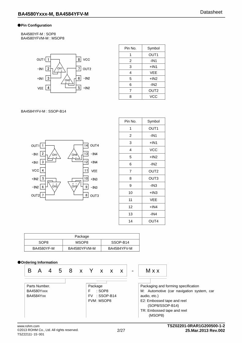
Pin Configuration BA4580YF-M : SOP8 BA4580YFVM-M : MSOP8
Pin No. Symbol
1 OUT1
2 -IN1
3 +IN1
4 VEE
5 +IN2
6 -IN2
7 OUT2
8 VCC
BA4584YFV-M : SSOP-B14
Pin No. Symbol
1 OUT1
2 -IN1
3 +IN1
4 VCC
5 +IN2
6 -IN2
7 OUT2
8 OUT3
9 -IN3
10 +IN3
11 VEE
12 +IN4
13 -IN4
14 OUT4
Package
SOP8 MSOP8 SSOP-B14
BA4580YF-M BA4580YFVM-M BA4584YFV-M
Ordering Information
B A 4 5 8 x Y x x x - M x x
Parts Number. BA4580Yxxx BA4584Yxx
Package F : SOP8 FV : SSOP-B14 FVM : MSOP8
Packaging and forming specification M: Automotive (car navigation system, car audio, etc.) E2: Embossed tape and reel (SOP8/SSOP-B14) TR: Embossed tape and reel (MSOP8)
7 8
6 9
5 10
4 11
3 12
2 13
1 14
CH4+ -
CH1- +
OUT1
-IN1
+IN1
VCC
OUT3
+IN3
-IN3
VEE
CH2- + + -
CH3
OUT4
-IN4
+IN4
OUT2
+IN2
-IN2
Datasheet
www.rohm.com TSZ02201-0RAR1G200500-1-2 ©2013 ROHM Co., Ltd. All rights reserved. 3/27 25.Mar.2013 Rev.002 TSZ22111・15・001
BA4580Yxxx-M, BA4584YFV-M
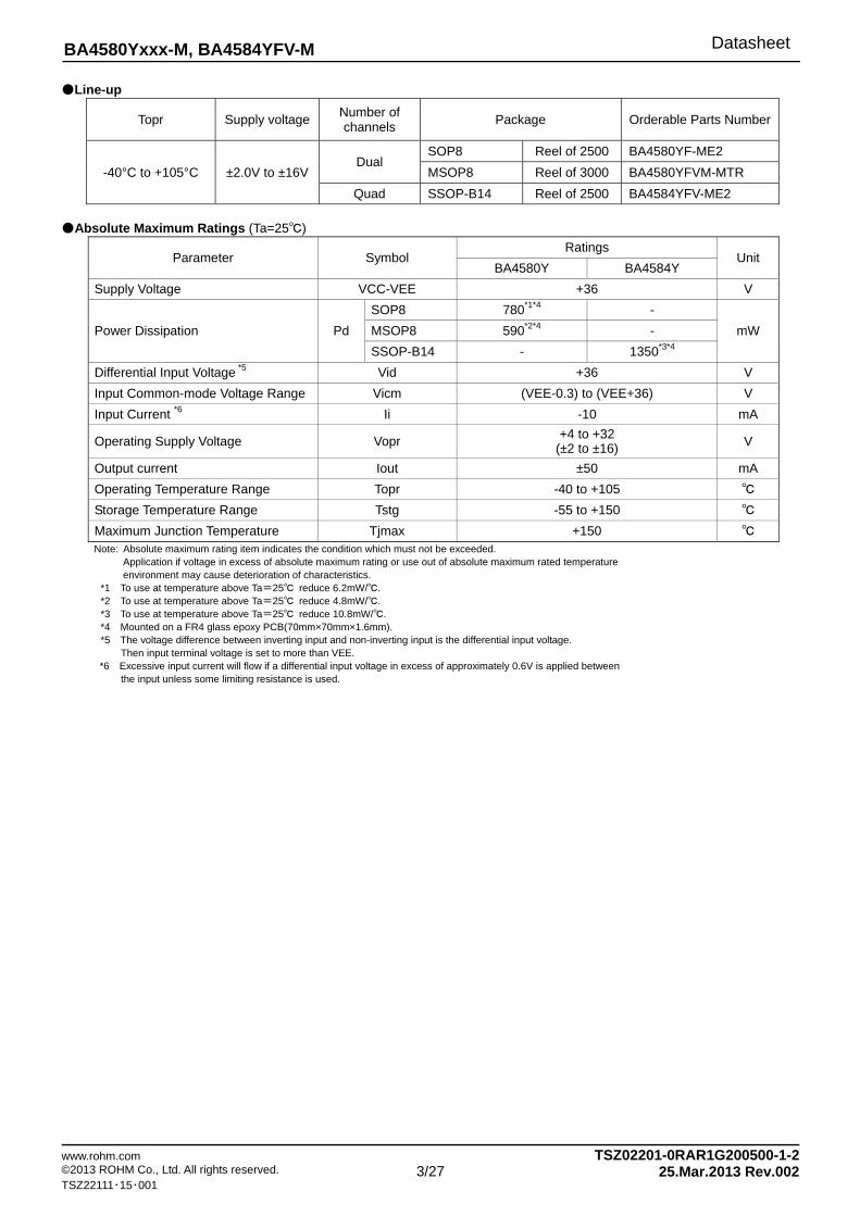
Line-up
Topr Supply voltage Number of channels
Package Orderable Parts Number
-40°C to +105°C ±2.0V to ±16V Dual
SOP8 Reel of 2500 BA4580YF-ME2
MSOP8 Reel of 3000 BA4580YFVM-MTR
Quad SSOP-B14 Reel of 2500 BA4584YFV-ME2
Absolute Maximum Ratings (Ta=25)
Parameter Symbol Ratings
Unit BA4580Y BA4584Y
Supply Voltage VCC-VEE +36 V
Power Dissipation Pd
SOP8 780*1*4 -
mW MSOP8 590*2*4 -
SSOP-B14 - 1350*3*4
Differential Input Voltage *5 Vid +36 V
Input Common-mode Voltage Range Vicm (VEE-0.3) to (VEE+36) V
Input Current *6 Ii -10 mA
Operating Supply Voltage Vopr +4 to +32
(±2 to ±16) V
Output current Iout ±50 mA
Operating Temperature Range Topr -40 to +105
Storage Temperature Range Tstg -55 to +150
Maximum Junction Temperature Tjmax +150 Note: Absolute maximum rating item indicates the condition which must not be exceeded. Application if voltage in excess of absolute maximum rating or use out of absolute maximum rated temperature environment may cause deterioration of characteristics.
*1 To use at temperature above Ta=25 reduce 6.2mW/. *2 To use at temperature above Ta=25 reduce 4.8mW/. *3 To use at temperature above Ta=25 reduce 10.8mW/. *4 Mounted on a FR4 glass epoxy PCB(70mm×70mm×1.6mm). *5 The voltage difference between inverting input and non-inverting input is the differential input voltage.
Then input terminal voltage is set to more than VEE. *6 Excessive input current will flow if a differential input voltage in excess of approximately 0.6V is applied between the input unless some limiting resistance is used.

Datasheet
www.rohm.com TSZ02201-0RAR1G200500-1-2 ©2013 ROHM Co., Ltd. All rights reserved. 4/27 25.Mar.2013 Rev.002 TSZ22111・15・001
BA4580Yxxx-M, BA4584YFV-M
Electrical Characteristics BA4580Yxxx-M (Unless otherwise specified VCC=+15V, VEE=-15V, Ta=25)
Parameter SymbolLimits
Unit Condition Min. Typ. Max.
Input Offset Voltage *7 Vio - 0.3 3 mV RS≦10kΩ
Input Offset Current *7 Iio - 5 200 nA -
Input Bias Current *8 Ib - 100 500 nA -
Supply Current ICC - 6 9 mA RL=∞, All Op-Amps, VIN+=0V
Maximum Output Voltage VOM ±12 ±13.5 - V RL≧2kΩ
Large Signal Voltage Gain Av 90 110 - dB RL≧10kΩ, OUT=±10V
Input Common-mode Voltage Range Vicm ±12 ±13.5 - V -
Common-mode Rejection Ratio CMRR 80 110 - dB RS≦10kΩ
Power Supply Rejection Ratio PSRR 80 110 - dB RS≦10kΩ
Slew Rate SR - 5 - V/μs RL≧2kΩ
Gain Band Width GBW - 10 - MHz f=10kHz
Unity Gain Frequency fT - 5 - MHz RL=2kΩ
Total Harmonic Distortion +Noise THD+N - 0.0005 - %
Av=20dB, OUT=5Vrms RL=2kΩ f=1kHz, 20Hz~20kHz BPF
Input Referred Noise Voltage Vn
- 5 - HznV/ RS=100Ω, Vi=0V, f=1kHz
- 0.8 - μVrms RIAA, RS=2.2 kΩ, 30kHz LPF
Channel Separation CS - 110 - dB R1=100Ω, f=1kHz
*7 Absolute value *8 Current direction: Since first input stage is composed with PNP transistor, input bias current flows out of IC.

Datasheet
www.rohm.com TSZ02201-0RAR1G200500-1-2 ©2013 ROHM Co., Ltd. All rights reserved. 5/27 25.Mar.2013 Rev.002 TSZ22111・15・001
BA4580Yxxx-M, BA4584YFV-M
BA4584Y (Unless otherwise specified VCC=+15V, VEE=-15V, Ta=25)
Parameter Symbol Limits
Unit Condition Min. Typ. Max.
Input Offset Voltage *9 Vio - 0.3 3 mV RS≦10kΩ
Input Offset Current *9 Iio - 5 200 nA -
Input Bias Current *10 Ib - 100 500 nA -
Supply Current ICC - 11 17 mA RL=∞, All Op-Amps, VIN+=0V
Maximum Output Voltage VOM ±12 ±13.5 - V RL≧2kΩ
Large Signal Voltage Gain AV 90 110 - dB RL≧10kΩ, OUT=±10V
Input Common-mode Voltage Range Vicm ±12 ±13.5 - V -
Common-mode Rejection Ratio CMRR 80 110 - dB RS≦10kΩ
Power Supply Rejection Ratio PSRR 80 110 - dB RS≦10kΩ
Slew Rate SR - 5 - V/μs RL≧2kΩ
Gain Band Width GBW - 10 - MHz f=10kHz
Unity Gain Frequency fT - 5 - MHz RL=2kΩ
Total Harmonic Distortion +Noise THD+N - 0.0005 - %
Av=20dB, OUT=5VrmsRL=2kΩ f=1kHz, 20Hz~20kHz BPF
Input Referred Noise Voltage Vn
- 5 - HznV/ RS=100Ω, Vi=0V, f=1kHz
- 0.8 - μVrms RIAA, RS=2.2kΩ, 30kHz LPF
Channel Separation CS - 110 - dB R1=100Ω, f=1kHz
*9 Absolute value *10 Current direction: Since first input stage is composed with PNP transistor, input bias current flows out of IC.

Datasheet
www.rohm.com TSZ02201-0RAR1G200500-1-2 ©2013 ROHM Co., Ltd. All rights reserved. 6/27 25.Mar.2013 Rev.002 TSZ22111・15・001
BA4580Yxxx-M, BA4584YFV-M
Description of electrical characteristics Described here are the terms of electric characteristics used in this datasheet. Items and symbols used are also shown. Note that item name and symbol and their meaning may differ from those on another manufacture’s document or general document. 1. Absolute maximum ratings
Absolute maximum rating item indicates the condition which must not be exceeded. Application of voltage in excess of absolute maximum rating or use out of absolute maximum rated temperature environment may cause deterioration of characteristics.
1.1 Power supply voltage (VCC-VEE)
Indicates the maximum voltage that can be applied between the positive power supply terminal and negative power supply terminal without deterioration or destruction of characteristics of internal circuit.
1.2 Differential input voltage (Vid) Indicates the maximum voltage that can be applied between non-inverting terminal and inverting terminal without deterioration and destruction of characteristics of IC.
1.3 Input common-mode voltage range (Vicm) Indicates the maximum voltage that can be applied to non-inverting terminal and inverting terminal without deterioration or destruction of characteristics. Input common-mode voltage range of the maximum ratings not assure normal operation of IC. When normal operation of IC is desired, the input common-mode voltage of characteristics item must be followed.
1.4 Power dissipation (Pd) Indicates the power that can be consumed by specified mounted board at the ambient temperature 25(normal temperature). As for package product, Pd is determined by the temperature that can be permitted by IC chip in the package (maximum junction temperature)and thermal resistance of the package.
2. Electrical characteristics item 2.1 Input offset voltage (Vio)
Indicates the voltage difference between non-inverting terminal and inverting terminal. It can be translated into the input voltage difference required for setting the output voltage at 0V.
2.2 Input offset current (Iio) Indicates the difference of input bias current between non-inverting terminal and inverting terminal.
2.3 Input bias current (Ib) Indicates the current that flows into or out of the input terminal. It is defined by the average of input bias current at non-inverting terminal and input bias current at inverting terminal.
2.4 Circuit current (ICC) Indicates the IC current that flows under specified conditions and no-load steady status.
2.5 Output saturation voltage (VOM) Signifies the voltage range that can be output under specific output conditions.
2.6 Large signal voltage gain (Av) Indicates the amplifying rate (gain) of output voltage against the voltage difference between non-inverting terminal
and Inverting terminal. It is normally the amplifying rate (gain) with reference to DC voltage. Av = (Output voltage) / (Differential Input voltage)
2.7 Input common-mode voltage range (Vicm) Indicates the input voltage range where IC operates normally.
2.8 Common-mode rejection ratio (CMRR) Indicates the ratio of fluctuation of input offset voltage when in-phase input voltage is changed. It is normally the fluctuation of DC. CMRR = (Change of Input common-mode voltage)/(Input offset fluctuation)
2.9 Power supply rejection ratio (PSRR) Indicates the ratio of fluctuation of input offset voltage when supply voltage is changed. It is normally the fluctuation of DC. PSRR = (Change of power supply voltage) / (Input offset fluctuation)
2.10 Slew Rate (SR) SR is a parameter that shows movement speed of operational amplifier. It indicates rate of variable output voltage as unit time.
2.11 Gain Band Width (GBW) The product of the open-loop voltage gain and the frequency at which the voltage gain decreases 6dB/octave.
2.12 Unity gain frequency (fT) Indicates a frequency where the voltage gain of operational amplifier is 1.
2.13 Total harmonic distortion + Noise (THD+N) Indicates the fluctuation of input offset voltage or that of output voltage with reference to the change of output voltage of driven channel.
2.14 Input referred noise voltage (Vn) Indicates a noise voltage generated inside the operational amplifier equivalent by ideal voltage source connected in series with input terminal.
2.15 Channel separation (CS) Indicates the fluctuation of input offset voltage or that of output voltage with reference to the change of output voltage of driven channel.

Datasheet
www.rohm.com TSZ02201-0RAR1G200500-1-2 ©2013 ROHM Co., Ltd. All rights reserved. 7/27 25.Mar.2013 Rev.002 TSZ22111・15・001
BA4580Yxxx-M, BA4584YFV-M
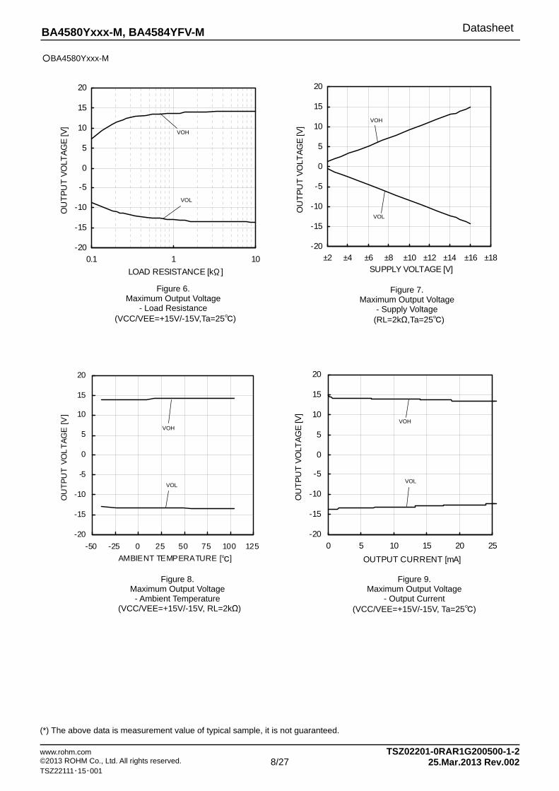
Typical Performance Curves BA4580Yxxx-M
(*) The above data is measurement value of typical sample, it is not guaranteed.
Figure 5. Maximum Output Voltage Swing
- Load Resistance (VCC/VEE=+15V/-15V,Ta=25)
0
5
10
15
20
25
30
0.1 1 10
LOAD RESISTANCE [kΩ]
MA
XIM
UM
OU
TP
UT
VO
LTA
GE
SW
ING
[VP
-P]
Figure 4. Supply Current - Ambient Temperature
0.0
2.0
4.0
6.0
8.0
10.0
-50 -25 0 25 50 75 100AMBIENT TEMPERATURE []
SU
PP
LY C
UR
RE
NT
[m
A]
±2 V
±15V
±7.5 V
Figure 2. Derating Curve
0
200
400
600
800
1000
0 25 50 75 100 125
AMBIENT TEMPERATURE [] .
PO
WE
R D
ISS
IPA
TIO
N [m
W]
.
BA4580YF-M
BA4580YFVM-M
Figure 3. Supply Current - Supply Voltage
105 0
2
4
6
8
10
±0 ±5 ±10 ±15 ±20
SUPPLY VOLTAGE [V]
SU
PP
LY
CU
RR
EN
T [m
A]
.
25
105
-40
Datasheet
www.rohm.com TSZ02201-0RAR1G200500-1-2 ©2013 ROHM Co., Ltd. All rights reserved. 8/27 25.Mar.2013 Rev.002 TSZ22111・15・001
BA4580Yxxx-M, BA4584YFV-M
BA4580Yxxx-M (*) The above data is measurement value of typical sample, it is not guaranteed.
Figure 9. Maximum Output Voltage
- Output Current (VCC/VEE=+15V/-15V, Ta=25)
-20
-15
-10
-5
0
5
10
15
20
0 5 10 15 20 25
OUTPUT CURRENT [mA]
OU
TP
UT
VO
LTA
GE
[V]
VOL
VOH
Figure 6. Maximum Output Voltage
- Load Resistance (VCC/VEE=+15V/-15V,Ta=25)
-20
-15
-10
-5
0
5
10
15
20
0.1 1 10
LOAD RESISTANCE [kΩ]
OU
TP
UT
VO
LTA
GE
[V]
VOL
VOH
Figure 8. Maximum Output Voltage - Ambient Temperature
(VCC/VEE=+15V/-15V, RL=2kΩ)
-20
-15
-10
-5
0
5
10
15
20
-50 -25 0 25 50 75 100 125
AMBIENT TEMPERATURE []
OU
TP
UT
VO
LT
AG
E [V
]
VOH
VOL
Figure 7. Maximum Output Voltage
- Supply Voltage (RL=2kΩ,Ta=25)
-20
-15
-10
-5
0
5
10
15
20
±2 ±4 ±6 ±8 ±10 ±12 ±14 ±16 ±18SUPPLY VOLTAGE [V]
OU
TP
UT
VO
LTA
GE
[V]
VOH
VOL

Datasheet
www.rohm.com TSZ02201-0RAR1G200500-1-2 ©2013 ROHM Co., Ltd. All rights reserved. 9/27 25.Mar.2013 Rev.002 TSZ22111・15・001
BA4580Yxxx-M, BA4584YFV-M
BA4580Yxxx-M (*) The above data is measurement value of typical sample, it is not guaranteed.
Figure 11. Input Offset Voltage - Ambient Temperature
(Vicm=0V, OUT=0V)
-6
-4
-2
0
2
4
6
-50 -25 0 25 50 75 100 125
AMBIENT TEMPERATURE []
INP
UT
OF
FS
ET
VO
LTA
GE
[mV
]
±2V
±7.5V
±15V
Figure 12. Input Bias Current - Supply Voltage
(Vicm=0V, OUT=0V)
0
20
40
60
80
100
120
140
160
180
200
±0 ±2 ±4 ±6 ±8 ±10 ±12 ±14 ±16
SUPPLY VOLTAGE [V]
INP
UT
BIA
S C
UR
RE
NT
[nA
]
.
-40
25 105
Figure 10. Input Offset Voltage - Supply Voltage
(Vicm=0V, OUT=0V)
-6
-4
-2
0
2
4
6
±0 ±2 ±4 ±6 ±8 ±10 ±12 ±14 ±16
SUPPLY VOLTAGE [V]
INP
UT
OF
FS
ET
VO
LTA
GE
[mV
]
-40
105
25
Figure 13. Input Bias Current - Ambient Temperature
(Vicm=0V, OUT=0V)
0
20
40
60
80
100
120
140
160
180
200
-50 -25 0 25 50 75 100 125
AMBIENT TEMPERATURE []
INP
UT
BIA
S C
UR
RE
NT
[nA
]
±15V
±7.5V
±2V
Datasheet
www.rohm.com TSZ02201-0RAR1G200500-1-2 ©2013 ROHM Co., Ltd. All rights reserved. 10/27 25.Mar.2013 Rev.002 TSZ22111・15・001
BA4580Yxxx-M, BA4584YFV-M
-5
-4
-3
-2
-1
0
1
2
3
4
5
-4 -3 -2 -1 0 1 2 3 4
INP
UT
OF
FS
ET
VO
LTA
GE
[mV
]
COMMON MODE INPUT VOLTAGE[V]
BA4580Yxxx-M (*) The above data is measurement value of typical sample, it is not guaranteed.
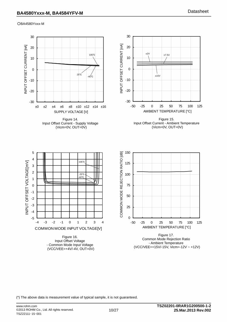
Figure 14. Input Offset Current - Supply Voltage
(Vicm=0V, OUT=0V)
-30
-20
-10
0
10
20
30
±0 ±2 ±4 ±6 ±8 ±10 ±12 ±14 ±16
SUPPLY VOLTAGE [V]
INP
UT
OF
FS
ET
CU
RR
EN
T [n
A]
.
105
-40 25
Figure 15. Input Offset Current - Ambient Temperature
(Vicm=0V, OUT=0V)
-30
-20
-10
0
10
20
30
-50 -25 0 25 50 75 100 125
AMBIENT TEMPERATURE [°C]
INP
UT
OF
FS
ET
CU
RR
EN
T [
nA
]
±2V
±15V
±7.5V
Figure 17. Common Mode Rejection Ratio
- Ambient Temperature (VCC/VEE=+15V/-15V, Vicm=-12V ~ +12V)
0
25
50
75
100
125
150
-50 -25 0 25 50 75 100 125AMBIENT TEMPERATURE [°C]
CO
MM
ON
MO
DE
RE
JEC
TIO
N R
AT
IO [
dB]
Figure 16. Input Offset Voltage
- Common Mode Input Voltage (VCC/VEE=+4V/-4V, OUT=0V)
105
25 -40

Datasheet
www.rohm.com TSZ02201-0RAR1G200500-1-2 ©2013 ROHM Co., Ltd. All rights reserved. 11/27 25.Mar.2013 Rev.002 TSZ22111・15・001
BA4580Yxxx-M, BA4584YFV-M
BA4580Yxxx-M (*) The above data is measurement value of typical sample, it is not guaranteed.
Figure 18. Power Supply Rejection Ratio
- Ambient Temperature (VCC/VEE=+2V/-2V ~ +15V/-15V)
0
25
50
75
100
125
150
-50 -25 0 25 50 75 100 125
AMBIENT TEMPERATURE []
PO
WE
R S
UP
PLY
RE
JEC
TIO
N R
AT
IO [d
B]
.
Figure 19. Slew Rate - Supply Voltage
(CL=100pF, RL=2kΩ, Ta=25)
-10
-5
0
5
10
±0 ±2 ±4 ±6 ±8 ±10 ±12 ±14 ±16SUPPLY VOLTAGE [V]
SLE
W R
AT
E [V
/μs]
.
SLE
W R
AT
E [
V/µ
s]
Figure 20. Equivalent Input Noise Voltage - Frequency
(VCC/VEE=+15V/-15V, RS=100Ω, Ta=25)
0
20
40
60
80
1 10 100 1000 10000
FREQUENCY [Hz]
EQ
UIV
ALE
NT
INP
UT
NO
ISE
VO
LTA
GE
[nV
/√H
z]
.
Figure 21. Total Harmonic Distortion - Output Voltage
(VCC/VEE=+15V/-15V, Av=20dB, RL=2kΩ, 80kHz-LPF, Ta=25)
0.0001
0.001
0.01
0.1
1
0.1 1 10OUTPUT VOLTAGE [Vrms]
TO
TA
L H
AR
MO
NIC
DIS
TO
RT
ION
[%
]
20kHz
20Hz
1kHz
Datasheet
www.rohm.com TSZ02201-0RAR1G200500-1-2 ©2013 ROHM Co., Ltd. All rights reserved. 12/27 25.Mar.2013 Rev.002 TSZ22111・15・001
BA4580Yxxx-M, BA4584YFV-M
BA4580Yxxx-M (*) The above data is measurement value of typical sample, it is not guaranteed.
Figure 22. Maximum Output Voltage Swing – Frequency (VCC/VEE=+15V/-15V, RL=2kΩ, Ta=25)
Figure 23. Voltage Gain, Phase - Frequency
(VCC/VEE=+15V/-15V, Av=40dB, RL=2kΩ, Ta=25)
0
10
20
30
40
50
60
1.E-01 1.E+00 1.E+01 1.E+02 1.E+03 1.E+04
FREQUENCY [Hz]
VO
LTA
GE
GA
IN [d
B]
-180
-150
-120
-90
-60
-30
0
PH
AS
E [d
eg]
GAIN
PHASE
102 103 104 105 106 107
0
5
10
15
20
25
30
MA
XIM
UM
OU
TP
UT
VO
LTA
GE
SW
ING
[Vp-
p]
FREQUENCY [kHz]
100 101 102 103
Datasheet
www.rohm.com TSZ02201-0RAR1G200500-1-2 ©2013 ROHM Co., Ltd. All rights reserved. 13/27 25.Mar.2013 Rev.002 TSZ22111・15・001
BA4580Yxxx-M, BA4584YFV-M
0
5
10
15
20
0 5 10 15 20 25 30 35
SU
PP
LY C
UR
RE
NT[
mA
]
SUPPLY VOLTAGE[V]
BA4584YFV-M (*) The above data is measurement value of typical sample, it is not guaranteed.
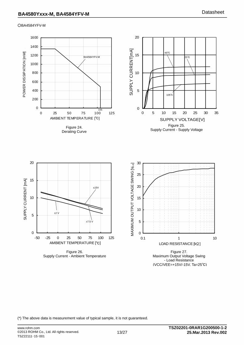
Figure 27. Maximum Output Voltage Swing
- Load Resistance (VCC/VEE=+15V/-15V, Ta=25)
0
5
10
15
20
25
30
0.1 1 10
LOAD RESISTANCE [kΩ]
MA
XIM
UM
OU
TP
UT
VO
LTA
GE
SW
ING
[VP
-P]
Figure 24. Derating Curve
0
200
400
600
800
1000
1200
1400
1600
0 25 50 75 100 125
AMBIENT TEMPERATURE [] .
PO
WE
R D
ISS
IPA
TIO
N [m
W]
.
105
BA4584YFV-M
Figure 26. Supply Current - Ambient Temperature
0
5
10
15
20
-50 -25 0 25 50 75 100 125AMBIENT TEMPERATURE []
SU
PP
LY C
UR
RE
NT
[mA
]
±2 V
±15V
±7.5 V
Figure 25. Supply Current - Supply Voltage
25
105
-40

Datasheet
www.rohm.com TSZ02201-0RAR1G200500-1-2 ©2013 ROHM Co., Ltd. All rights reserved. 14/27 25.Mar.2013 Rev.002 TSZ22111・15・001
BA4580Yxxx-M, BA4584YFV-M
BA4584YFV-M (*) The above data is measurement value of typical sample, it is not guaranteed.
VOH
Figure 29. Maximum Output Voltage
- Supply Voltage (RL=2kΩ, Ta=25)
-20
-15
-10
-5
0
5
10
15
20
±2 ±4 ±6 ±8 ±10 ±12 ±14 ±16 ±18SUPPLY VOLTAGE [V]
OU
TP
UT
VO
LTA
GE
[V]
VOL
Figure 31. Maximum Output Voltage
- Output Current (VCC/VEE=+15V/-15V, Ta=25)
-20
-15
-10
-5
0
5
10
15
20
0 5 10 15 20 25
OUTPUT CURRENT [mA]
OU
TP
UT
VO
LTA
GE
[V]
VOL
VOH
Figure 28. Maximum Output Voltage
- Load Resistance (VCC/VEE=+15V/-15V, Ta=25)
-20
-15
-10
-5
0
5
10
15
20
0.1 1 10
LOAD RESISTANCE [kΩ]
OU
TP
UT
VO
LTA
GE
[V]
VOL
VOH
Figure 30. Maximum Output Voltage - Ambient Temperature
(VCC/VEE=+15V/-15V, RL=2kΩ)
-20
-15
-10
-5
0
5
10
15
20
-50 -25 0 25 50 75 100 125
AMBIENT TEMPERATURE []
OU
TP
UT
VO
LT
AG
E [V
]
VOH
VOL
Datasheet
www.rohm.com TSZ02201-0RAR1G200500-1-2 ©2013 ROHM Co., Ltd. All rights reserved. 15/27 25.Mar.2013 Rev.002 TSZ22111・15・001
BA4580Yxxx-M, BA4584YFV-M
BA4584YFV-M (*) The above data is measurement value of typical sample, it is not guaranteed.
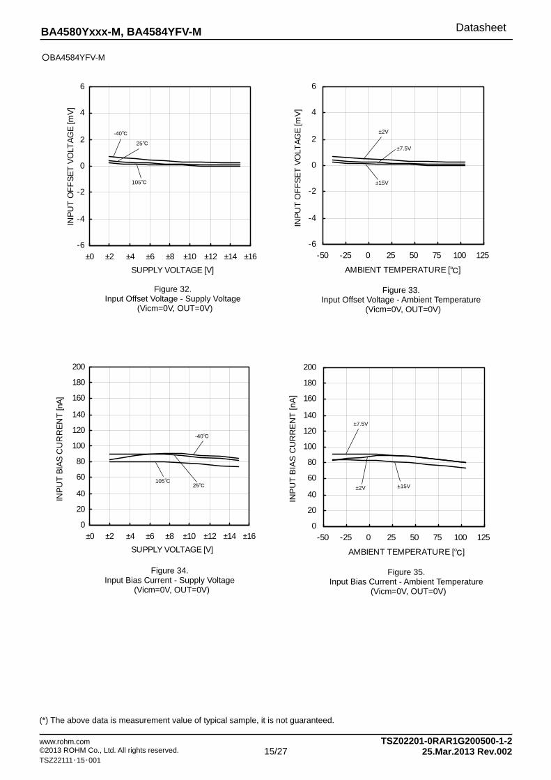
Figure 33. Input Offset Voltage - Ambient Temperature
(Vicm=0V, OUT=0V)
-6
-4
-2
0
2
4
6
-50 -25 0 25 50 75 100 125
AMBIENT TEMPERATURE []
INP
UT
OF
FS
ET
VO
LTA
GE
[mV
]
±2V
±7.5V
±15V
Figure 34. Input Bias Current - Supply Voltage
(Vicm=0V, OUT=0V)
0
20
40
60
80
100
120
140
160
180
200
±0 ±2 ±4 ±6 ±8 ±10 ±12 ±14 ±16
SUPPLY VOLTAGE [V]
INP
UT
BIA
S C
UR
RE
NT
[nA
]
.
-40
25 105
Figure 32. Input Offset Voltage - Supply Voltage
(Vicm=0V, OUT=0V)
-6
-4
-2
0
2
4
6
±0 ±2 ±4 ±6 ±8 ±10 ±12 ±14 ±16
SUPPLY VOLTAGE [V]
INP
UT
OF
FS
ET
VO
LTA
GE
[mV
]
-40
105
25
Figure 35. Input Bias Current - Ambient Temperature
(Vicm=0V, OUT=0V)
0
20
40
60
80
100
120
140
160
180
200
-50 -25 0 25 50 75 100 125
AMBIENT TEMPERATURE []
INP
UT
BIA
S C
UR
RE
NT
[nA
]
±15V
±7.5V
±2V

Datasheet
www.rohm.com TSZ02201-0RAR1G200500-1-2 ©2013 ROHM Co., Ltd. All rights reserved. 16/27 25.Mar.2013 Rev.002 TSZ22111・15・001
BA4580Yxxx-M, BA4584YFV-M
-5
-4
-3
-2
-1
0
1
2
3
4
5
-4 -3 -2 -1 0 1 2 3 4
INP
UT
OF
FS
ET
VO
LTA
GE
[mV
]
COMMON MODE INPUT VOLTAGE[V]
BA4584YFV-M (*) The above data is measurement value of typical sample, it is not guaranteed.
Figure 37. Input Offset Current - Ambient Temperature
(Vicm=0V, OUT=0V)
-30
-20
-10
0
10
20
30
-50 -25 0 25 50 75 100 125
AMBIENT TEMPERATURE [°C]
INP
UT
OF
FS
ET
CU
RR
EN
T [n
A]
±2V
±15V
±7.5V
Figure 39. Common Mode Rejection Ratio
- Ambient Temperature (VCC/VEE=+15V/-15V, Vicm=-12V ~ +12V)
0
25
50
75
100
125
150
-50 -25 0 25 50 75 100 125AMBIENT TEMPERATURE [°C]
CO
MM
ON
MO
DE
RE
JEC
TIO
N R
AT
IO [
dB]
Figure 36. Input Offset Current - Supply Voltage
(Vicm=0V, OUT=0V)
-30
-20
-10
0
10
20
30
±0 ±2 ±4 ±6 ±8 ±10 ±12 ±14 ±16
SUPPLY VOLTAGE [V]
INP
UT
OF
FS
ET
CU
RR
EN
T [n
A]
.
105
-40 25
Figure 38. Input Offset Voltage
- Common Mode Input Voltage (VCC/VEE=+4V/-4V, OUT=0V)
105
25
-40

Datasheet
www.rohm.com TSZ02201-0RAR1G200500-1-2 ©2013 ROHM Co., Ltd. All rights reserved. 17/27 25.Mar.2013 Rev.002 TSZ22111・15・001
BA4580Yxxx-M, BA4584YFV-M
BA4584YFV-M (*) The above data is measurement value of typical sample, it is not guaranteed.
Figure 40. Power Supply Rejection Ratio
- Ambient Temperature (VCC/VEE=+2V/-2V ~ +15V/-15V)
0
25
50
75
100
125
150
-50 -25 0 25 50 75 100 125
AMBIENT TEMPERATURE []
PO
WE
R S
UP
PLY
RE
JEC
TIO
N R
AT
IO [d
B]
.
Figure 41. Slew Rate - Supply Voltage
(CL=100pF, RL=2kΩ, Ta=25)
-10
-5
0
5
10
±0 ±2 ±4 ±6 ±8 ±10 ±12 ±14 ±16SUPPLY VOLTAGE [V]
SLE
W R
AT
E [V
/μs]
.
SL
EW
RA
TE
[V/µ
s]
Figure 42. Equivalent Input Noise Voltage - Frequency
(VCC/VEE=+15V/-15V, RS=100Ω, Ta=25)
0
20
40
60
80
1 100 10000
FREQUENCY [Hz]
EQ
UIV
ALE
NT
INP
UT
NO
ISE
VO
LTA
GE
[nV
/√H
z]
.
Figure 43. Total Harmonic Distortion - Output Voltage
(VCC/VEE=+15V/-15V, Av=20dB, RL=2kΩ, 80kHz-LPF, Ta=25)
0.0001
0.001
0.01
0.1
1
0.1 1 10OUTPUT VOLTAGE [Vrms]
TO
TA
L H
AR
MO
NIC
DIS
TO
RT
ION
[%
]
20kHz
20Hz
1kHz
Datasheet
www.rohm.com TSZ02201-0RAR1G200500-1-2 ©2013 ROHM Co., Ltd. All rights reserved. 18/27 25.Mar.2013 Rev.002 TSZ22111・15・001
BA4580Yxxx-M, BA4584YFV-M
BA4584YFV-M (*) The above data is measurement value of typical sample, it is not guaranteed.
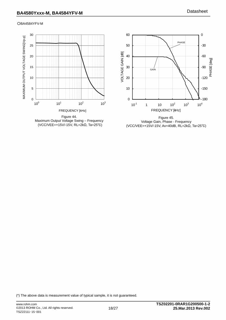
Figure 44. Maximum Output Voltage Swing – Frequency (VCC/VEE=+15V/-15V, RL=2kΩ, Ta=25)
Figure 45. Voltage Gain, Phase - Frequency
(VCC/VEE=+15V/-15V, Av=40dB, RL=2kΩ, Ta=25)
0
10
20
30
40
50
60
1.E-01 1.E+00 1.E+01 1.E+02 1.E+03 1.E+04
FREQUENCY [kHz]
VO
LTA
GE
GA
IN [d
B]
-180
-150
-120
-90
-60
-30
0
PH
AS
E [d
eg]
GAIN
PHASE
10-1 1 10 102 103 104
0
5
10
15
20
25
30
MA
XIM
UM
OU
TP
UT
VO
LTA
GE
SW
ING
[Vp-
p]
FREQUENCY [kHz]
100 101 102 103

Datasheet
www.rohm.com TSZ02201-0RAR1G200500-1-2 ©2013 ROHM Co., Ltd. All rights reserved. 19/27 25.Mar.2013 Rev.002 TSZ22111・15・001
BA4580Yxxx-M, BA4584YFV-M
Power Dissipation Power dissipation (total loss) indicates the power that the IC can consume at Ta=25°C (normal temperature). As the IC consumes power, it heats up, causing its temperature to be higher than the ambient temperature. The allowable temperature that the IC can accept is limited. This depends on the circuit configuration, manufacturing process, and consumable power. Power dissipation is determined by the allowable temperature within the IC (maximum junction temperature) and the thermal resistance of the package used (heat dissipation capability). Maximum junction temperature is typically equal to the maximum storage temperature. The heat generated through the consumption of power by the IC radiates from the mold resin or lead frame of the package. Thermal resistance, represented by the symbol θja°C/W, indicates this heat dissipation capability. Similarly, the temperature of an IC inside its package can be estimated by thermal resistance. Figure 46. (a) shows the model of the thermal resistance of the package. The equation below shows how to compute for the Thermal resistance (θja), given the ambient temperature (Ta), maximum junction temperature (Tjmax), and power dissipation (Pd). θja = (Tjmax - Ta) / Pd /W ・・・・・ (Ⅰ) The Derating curve in Figure 46. (b) indicates the power that the IC can consume with reference to ambient temperature. Power consumption of the IC begins to attenuate at certain temperatures. This gradient is determined by Thermal resistance (θja), which depends on the chip size, power consumption, package, ambient temperature, package condition, wind velocity, etc. This may also vary even when the same of package is used. Thermal reduction curve indicates a reference value measured at a specified condition. Figure 47. (c),(d) shows an example of the derating curve for BA4580Yxxx-M, BA4584YFV-M.
Figure 46. Thermal resistance and derating
( *11 ) ( *12 ) (*13) Unit
6.2 4.8 10.8 mW/ When using the unit above Ta=25, subtract the value above per Celsius degree . Mounted on a FR4 glass epoxy board 70mm×70mm×1.6mm(cooper foil area below 3%)
Figure 47. Derating curve
(a) Thermal resistance (b) Derating curve
(c) BA4580Yxxx-M
0
200
400
600
800
1000
0 25 50 75 100 125AMBIENT TEMPERATURE [] .
PO
WE
R D
ISS
IPA
TIO
N [m
W]
. BA4580YF-M(*11)
BA4580YFVM-M(*12)
0
200
400
600
800
1000
1200
1400
1600
0 25 50 75 100 125AMBIENT TEMPERATURE [] .
PO
WE
R D
ISS
IPA
TIO
N [m
W]
.
BA4584YFV-M(*13)
(d) BA4584YFV-M
0 50 75 100 125 15025
P1
P2
Pd (max)
LSIの消費電力 [W]
θ' ja2
θ' ja1Tj ' (max)
θja2 < θja1
周囲温度 Ta [ ]
θ ja2
θ ja1
Tj (max)
Power dissipation of LSI
Ambient temperature
Ambient temperature Ta
Chip surface temperature Tj []
Power dissipation Pd[W]
θja = ( Tjmax - Ta) / Pd /W
[]

Datasheet
www.rohm.com TSZ02201-0RAR1G200500-1-2 ©2013 ROHM Co., Ltd. All rights reserved. 20/27 25.Mar.2013 Rev.002 TSZ22111・15・001
BA4580Yxxx-M, BA4584YFV-M
Application Information NULL method condition for Test circuit1
VCC, VEE, EK Unit: V
Parameter VF S1 S2 S3BA4580Y BA4584Y
calculationVCC VEE EK VCC VEE EK
Input Offset Voltage VF1 ON ON OFF 15 -15 0 15 -15 0 1
Input Offset Current VF2 OFF OFF OFF 15 -15 0 15 -15 0 2
Input Bias Current VF3 OFF ON
OFF 15 -15 0 15 -15 0 3 VF4 ON OFF
Large Signal Voltage Gain VF5
ON ON ON15 -15 -10 15 -15 -10
4 VF6 15 -15 10 15 -15 10
Common-mode Rejection Ratio (Input common-mode Voltage Range)
VF7 ON ON OFF
3 -27 12 3 -27 12 5
VF8 27 -3 -12 27 -3 -12
Power Supply Rejection Ratio
VF9 ON ON OFF
4 -2 0 2 -2 0 6
VF10 15 -15 0 15 -15 0
- Calculation - 1. Input Offset Voltage (Vio) 2. Input Offset Current (Iio) 3. Input Bias Current (Ib) 4. Large Signal Voltage Gain (Av) 5. Common-mode Rejection Ration (CMRR) 6. Power supply rejection ratio (PSRR)
Figure 48. Test circuit1 (one channel only)
[V]RS / RF + 1
VF1Vio
[A]RS) / RF + (1× Ri
VF1-VF2 Iio
[A]RS) / RF + (1 ×Ri×2
VF3-VF4 Ib
[dB]VF6-VF5
RF/RS)+(1×ΔEKLog×20 Av
[dB]VF7-VF8
RF/RS)+(1×ΔVicmLog×20 CMRR
[dB]VF9-VF10
RF/RS)+(1×ΔVccLog×20 PSRR
VCC
RF=50kΩ
Ri=10kΩRS=50Ω
RL
SW2
500kΩ
500kΩ 0.1µF
EK 15V
DUT
VEE 50kΩ
Vicm
SW1
Ri=10kΩ
Vo
VFRS=50Ω 1000pF
0.1µF
-15V
NULL SW3

Datasheet
www.rohm.com TSZ02201-0RAR1G200500-1-2 ©2013 ROHM Co., Ltd. All rights reserved. 21/27 25.Mar.2013 Rev.002 TSZ22111・15・001
BA4580Yxxx-M, BA4584YFV-M
Switch Condition for Test Circuit 2
SW No. SW1 SW2 SW3 SW4 SW5 SW6 SW7 SW8 SW9 SW10 SW11 SW12 SW13 SW14
Supply Current OFF OFF OFF ON OFF ON OFF OFF OFF OFF OFF OFF OFF OFF
Maximum Output Voltage (high) OFF OFF ON OFF OFF ON OFF OFF ON OFF OFF OFF ON OFF
Maximum Output Voltage (Low) OFF OFF ON OFF OFF ON OFF OFF OFF OFF OFF OFF ON OFF
Output Source Current OFF OFF ON OFF OFF ON OFF OFF OFF OFF OFF OFF OFF ON
Output Sink Current OFF OFF ON OFF OFF ON OFF OFF OFF OFF OFF OFF OFF ON
Slew Rate OFF OFF OFF ON OFF OFF OFF ON ON ON OFF OFF OFF OFF
Gain Band Width OFF ON OFF OFF ON ON OFF OFF ON ON OFF OFF OFF OFF
Input Referred Noise Voltage ON OFF OFF OFF ON ON OFF OFF OFF OFF ON OFF OFF OFF
VCC
VEE
R1V
R2
R1//R2
VOUT1=0.5[Vrms]
VIN
VCC
VEE
R1V
R2
R1//R2
VOUT2
OTHERCH
CS=20×log100×VOUT1
VOUT2
Figure 50. Slew Rate Input Waveform
Figure 51. Test Circuit 3(Channel Separation)
Figure 49. Test Circuit 2 (each Op-Amp)
C
(R1=1kΩ, R2=100kΩ)
40dB amplifier
OUT1 =0.5Vrms
OUT2
OUT2
OUT1100log20CS
VH
VL
Input wave t
Input voltage
VH
VL
Δ t
ΔV
Output wave
SR=ΔV/Δt
t
Output voltage
90%
10%
Datasheet
www.rohm.com TSZ02201-0RAR1G200500-1-2 ©2013 ROHM Co., Ltd. All rights reserved. 22/27 25.Mar.2013 Rev.002 TSZ22111・15・001
BA4580Yxxx-M, BA4584YFV-M
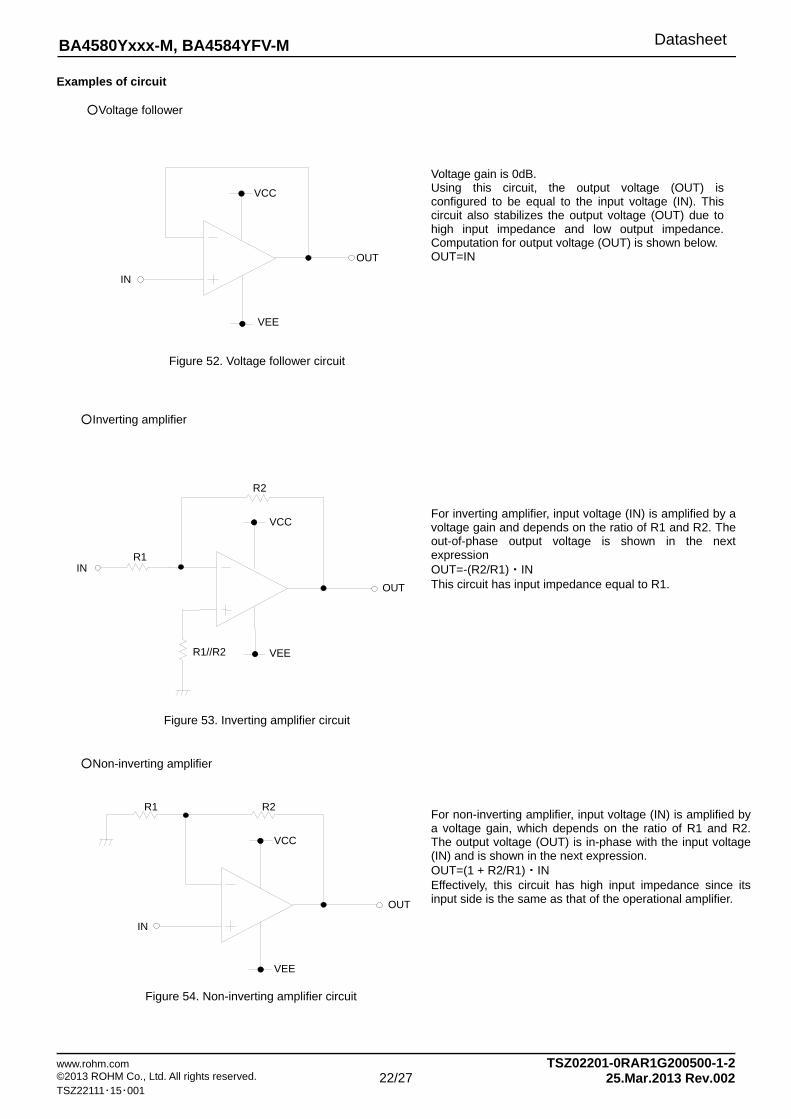
Examples of circuit
Voltage follower
Inverting amplifier
Non-inverting amplifier
Figure 52. Voltage follower circuit
Figure 53. Inverting amplifier circuit
Figure 54. Non-inverting amplifier circuit
Voltage gain is 0dB. Using this circuit, the output voltage (OUT) isconfigured to be equal to the input voltage (IN). Thiscircuit also stabilizes the output voltage (OUT) due tohigh input impedance and low output impedance.Computation for output voltage (OUT) is shown below.OUT=IN
For inverting amplifier, input voltage (IN) is amplified by avoltage gain and depends on the ratio of R1 and R2. Theout-of-phase output voltage is shown in the nextexpression OUT=-(R2/R1)・IN This circuit has input impedance equal to R1.
For non-inverting amplifier, input voltage (IN) is amplified bya voltage gain, which depends on the ratio of R1 and R2.The output voltage (OUT) is in-phase with the input voltage(IN) and is shown in the next expression. OUT=(1 + R2/R1)・IN Effectively, this circuit has high input impedance since itsinput side is the same as that of the operational amplifier.
VEE
OUT
IN
VCC
R2
R1
VEER1//R2
IN
OUT
VCC
VEE
R2
VCC
IN
OUT
R1

Datasheet
www.rohm.com TSZ02201-0RAR1G200500-1-2 ©2013 ROHM Co., Ltd. All rights reserved. 23/27 25.Mar.2013 Rev.002 TSZ22111・15・001
BA4580Yxxx-M, BA4584YFV-M
Operational Notes 1) Processing of unused circuit
It is recommended to apply connection (see the Figure 55.) and set the non inverting input terminal at the potential within input common-mode voltage range (Vicm), for any unused circuit.
2) Input voltage
Applying (VEE - 0.3) to (VEE + 36)V (BA4558R) to the input terminal is possible without causing deterioration of the electrical characteristics or destruction, irrespective of the supply voltage. However, this does not ensure normal circuit operation. Please note that the circuit operates normally only when the input voltage is within the common mode input voltage range of the electric characteristics.
3) Maximum output voltage
Because the output voltage range becomes narrow as the output current Increases, design the application with margin by considering changes in electrical characteristics and temperature characteristics.
4) Short-circuit of output terminal
When output terminal and VCC or VEE terminal are shorted, excessive Output current may flow under some conditions, and heating may destroy IC. It is necessary to connect a resistor as shown in Figure 56., thereby protecting against load shorting.
5) Power supply (split supply / single supply) in used
Op-amp operates when specified voltage is applied between VCC and VEE. Therefore, the single supply Op-Amp can be used for double supply Op-Amp as well.
6) Power dissipation (Pd)
Use a thermal design that allows for a sufficient margin in light of the power dissipation (Pd) in actual operating conditions.
7) Short-circuit between pins and wrong mounting
Pay attention to the assembly direction of the ICs. Wrong mounting direction or shorts between terminals, GND, or other components on the circuits, can damage the IC.
8) Use in strong electromagnetic field
Using the ICs in strong electromagnetic field can cause operation malfunction. 9) Radiation
This IC is not designed to be radiation-resistant.
10) IC Handling When stress is applied to IC because of deflection or bend of board, the characteristics may fluctuate due to piezo resistance effects.
11) Inspection on set board
During testing, turn on or off the power before mounting or dismounting the board from the test Jig. Do not power up the board without waiting for the output capacitors to discharge. The capacitors in the low output impedance terminal can stress the device. Pay attention to the electro static voltages during IC handling, transportation, and storage.
12) Output capacitor
When VCC terminal is shorted to VEE (GND) potential and an electric charge has accumulated on the external capacitor, connected to output terminal, accumulated charge may be discharged VCC terminal via the parasitic element within the circuit or terminal protection element. The element in the circuit may be damaged (thermal destruction). When using this IC for an application circuit where there is oscillation, output capacitor load does not occur, as when using this IC as a voltage comparator. Set the capacitor connected to output terminal below 0.1μF in order to prevent damage to IC.
application circuit for unused op-ampFigure 55. The example of
Figure 56. The example of output short protection
Connect
to Vicm
VCC
VEE
Vicm -
+
VEE
VCC
+
-
protection
resistor

Datasheet
www.rohm.com TSZ02201-0RAR1G200500-1-2 ©2013 ROHM Co., Ltd. All rights reserved. 24/27 25.Mar.2013 Rev.002 TSZ22111・15・001
BA4580Yxxx-M, BA4584YFV-M
Physical Dimension, Tape and Reel Information
Package Name SOP8
∗ Order quantity needs to be multiple of the minimum quantity.
<Tape and Reel information>
Embossed carrier tapeTape
Quantity
Direction of feed The direction is the 1pin of product is at the upper left when you hold
reel on the left hand and you pull out the tape on the right hand
2500pcs
E2
( )
Direction of feed
Reel1pin
(UNIT : mm) PKG : SOP8 Drawing No. : EX112-5001-1
(Max 5.35 (include.BURR))

Datasheet
www.rohm.com TSZ02201-0RAR1G200500-1-2 ©2013 ROHM Co., Ltd. All rights reserved. 25/27 25.Mar.2013 Rev.002 TSZ22111・15・001
BA4580Yxxx-M, BA4584YFV-M
Physical Dimension, Tape and Reel Information
Package Name MSOP8
Direction of feed
Reel ∗ Order quantity needs to be multiple of the minimum quantity.
<Tape and Reel information>
Embossed carrier tapeTape
Quantity
Direction of feed
The direction is the 1pin of product is at the upper right when you hold reel on the left hand and you pull out the tape on the right hand
3000pcs
TR
( )1pin

Datasheet
www.rohm.com TSZ02201-0RAR1G200500-1-2 ©2013 ROHM Co., Ltd. All rights reserved. 26/27 25.Mar.2013 Rev.002 TSZ22111・15・001
BA4580Yxxx-M, BA4584YFV-M
Physical Dimension, Tape and Reel Information
Package Name SSOP-B14
∗ Order quantity needs to be multiple of the minimum quantity.
<Tape and Reel information>
Embossed carrier tapeTape
Quantity
Direction of feed
The direction is the 1pin of product is at the upper left when you hold reel on the left hand and you pull out the tape on the right hand
2500pcs
E2
( )
Direction of feed
Reel1pin

Datasheet
www.rohm.com TSZ02201-0RAR1G200500-1-2 ©2013 ROHM Co., Ltd. All rights reserved. 27/27 25.Mar.2013 Rev.002 TSZ22111・15・001
BA4580Yxxx-M, BA4584YFV-M
Marking Diagram
Land pattern data
All dimensions in mm
PKG Land pitch
e Land space
MIE Land length
≧ℓ 2 Land width
b2
SOP8 1.27 4.60 1.10 0.76
MSOP8 0.65 2.62 0.99 0.35
SSOP-B14 0.65 4.60 1.20 0.35
Revision History
Date Revision Changes
2012. 7. 6 001 New Release
2013. 3. 25 002 Added BA4580Y
Product Name Package Type Marking
BA4580Y F-M SOP8 80YM
FVM-M MSOP8 80YM BA4584Y FV-M SSOP-B14 4584Y
SOP8(TOP VIEW)
Part Number Marking
LOT Number
1PIN MARK
MSOP8(TOP VIEW)
Part Number Marking
LOT Number
1PIN MARK
b 2
MIE
e
ℓ2
SOP8, SSOP-B8, MSOP8
SSOP-B14(TOP VIEW)
Part Number Marking
LOT Number
1PIN MARK
DatasheetDatasheet
Notice - SS Rev.002© 2014 ROHM Co., Ltd. All rights reserved.
Notice Precaution on using ROHM Products
1. If you intend to use our Products in devices requiring extremely high reliability (such as medical equipment (Note 1), aircraft/spacecraft, nuclear power controllers, etc.) and whose malfunction or failure may cause loss of human life, bodily injury or serious damage to property (“Specific Applications”), please consult with the ROHM sales representative in advance. Unless otherwise agreed in writing by ROHM in advance, ROHM shall not be in any way responsible or liable for any damages, expenses or losses incurred by you or third parties arising from the use of any ROHM’s Products for Specific Applications.
(Note1) Medical Equipment Classification of the Specific Applications JAPAN USA EU CHINA
CLASSⅢ CLASSⅢ
CLASSⅡb CLASSⅢ
CLASSⅣ CLASSⅢ
2. ROHM designs and manufactures its Products subject to strict quality control system. However, semiconductor
products can fail or malfunction at a certain rate. Please be sure to implement, at your own responsibilities, adequate safety measures including but not limited to fail-safe design against the physical injury, damage to any property, which a failure or malfunction of our Products may cause. The following are examples of safety measures:
[a] Installation of protection circuits or other protective devices to improve system safety [b] Installation of redundant circuits to reduce the impact of single or multiple circuit failure
3. Our Products are not designed under any special or extraordinary environments or conditions, as exemplified below. Accordingly, ROHM shall not be in any way responsible or liable for any damages, expenses or losses arising from the use of any ROHM’s Products under any special or extraordinary environments or conditions. If you intend to use our Products under any special or extraordinary environments or conditions (as exemplified below), your independent verification and confirmation of product performance, reliability, etc, prior to use, must be necessary:
[a] Use of our Products in any types of liquid, including water, oils, chemicals, and organic solvents [b] Use of our Products outdoors or in places where the Products are exposed to direct sunlight or dust [c] Use of our Products in places where the Products are exposed to sea wind or corrosive gases, including Cl2,
H2S, NH3, SO2, and NO2
[d] Use of our Products in places where the Products are exposed to static electricity or electromagnetic waves [e] Use of our Products in proximity to heat-producing components, plastic cords, or other flammable items [f] Sealing or coating our Products with resin or other coating materials [g] Use of our Products without cleaning residue of flux (even if you use no-clean type fluxes, cleaning residue of
flux is recommended); or Washing our Products by using water or water-soluble cleaning agents for cleaning residue after soldering
[h] Use of the Products in places subject to dew condensation
4. The Products are not subject to radiation-proof design. 5. Please verify and confirm characteristics of the final or mounted products in using the Products. 6. In particular, if a transient load (a large amount of load applied in a short period of time, such as pulse. is applied,
confirmation of performance characteristics after on-board mounting is strongly recommended. Avoid applying power exceeding normal rated power; exceeding the power rating under steady-state loading condition may negatively affect product performance and reliability.
7. De-rate Power Dissipation (Pd) depending on Ambient temperature (Ta). When used in sealed area, confirm the actual
ambient temperature. 8. Confirm that operation temperature is within the specified range described in the product specification. 9. ROHM shall not be in any way responsible or liable for failure induced under deviant condition from what is defined in
this document.
Precaution for Mounting / Circuit board design 1. When a highly active halogenous (chlorine, bromine, etc.) flux is used, the residue of flux may negatively affect product
performance and reliability. 2. In principle, the reflow soldering method must be used; if flow soldering method is preferred, please consult with the
ROHM representative in advance. For details, please refer to ROHM Mounting specification

DatasheetDatasheet
Notice - SS Rev.002© 2014 ROHM Co., Ltd. All rights reserved.
Precautions Regarding Application Examples and External Circuits 1. If change is made to the constant of an external circuit, please allow a sufficient margin considering variations of the
characteristics of the Products and external components, including transient characteristics, as well as static characteristics.
2. You agree that application notes, reference designs, and associated data and information contained in this document
are presented only as guidance for Products use. Therefore, in case you use such information, you are solely responsible for it and you must exercise your own independent verification and judgment in the use of such information contained in this document. ROHM shall not be in any way responsible or liable for any damages, expenses or losses incurred by you or third parties arising from the use of such information.
Precaution for Electrostatic
This Product is electrostatic sensitive product, which may be damaged due to electrostatic discharge. Please take proper caution in your manufacturing process and storage so that voltage exceeding the Products maximum rating will not be applied to Products. Please take special care under dry condition (e.g. Grounding of human body / equipment / solder iron, isolation from charged objects, setting of Ionizer, friction prevention and temperature / humidity control).
Precaution for Storage / Transportation 1. Product performance and soldered connections may deteriorate if the Products are stored in the places where:
[a] the Products are exposed to sea winds or corrosive gases, including Cl2, H2S, NH3, SO2, and NO2 [b] the temperature or humidity exceeds those recommended by ROHM [c] the Products are exposed to direct sunshine or condensation [d] the Products are exposed to high Electrostatic
2. Even under ROHM recommended storage condition, solderability of products out of recommended storage time period may be degraded. It is strongly recommended to confirm solderability before using Products of which storage time is exceeding the recommended storage time period.
3. Store / transport cartons in the correct direction, which is indicated on a carton with a symbol. Otherwise bent leads
may occur due to excessive stress applied when dropping of a carton. 4. Use Products within the specified time after opening a humidity barrier bag. Baking is required before using Products of
which storage time is exceeding the recommended storage time period.
Precaution for Product Label QR code printed on ROHM Products label is for ROHM’s internal use only.
Precaution for Disposition When disposing Products please dispose them properly using an authorized industry waste company.
Precaution for Foreign Exchange and Foreign Trade act Since our Products might fall under controlled goods prescribed by the applicable foreign exchange and foreign trade act, please consult with ROHM representative in case of export.
Precaution Regarding Intellectual Property Rights 1. All information and data including but not limited to application example contained in this document is for reference
only. ROHM does not warrant that foregoing information or data will not infringe any intellectual property rights or any other rights of any third party regarding such information or data. ROHM shall not be in any way responsible or liable for infringement of any intellectual property rights or other damages arising from use of such information or data.:
2. No license, expressly or implied, is granted hereby under any intellectual property rights or other rights of ROHM or any
third parties with respect to the information contained in this document.
Other Precaution 1. This document may not be reprinted or reproduced, in whole or in part, without prior written consent of ROHM. 2. The Products may not be disassembled, converted, modified, reproduced or otherwise changed without prior written
consent of ROHM. 3. In no event shall you use in any way whatsoever the Products and the related technical information contained in the
Products or this document for any military purposes, including but not limited to, the development of mass-destruction weapons.
4. The proper names of companies or products described in this document are trademarks or registered trademarks of
ROHM, its affiliated companies or third parties.

DatasheetDatasheet
Notice – WE Rev.001© 2014 ROHM Co., Ltd. All rights reserved.
General Precaution 1. Before you use our Pro ducts, you are requested to care fully read this document and fully understand its contents.
ROHM shall n ot be in an y way responsible or liabl e for fa ilure, malfunction or acci dent arising from the use of a ny ROHM’s Products against warning, caution or note contained in this document.
2. All information contained in this docume nt is current as of the issuing date and subj ect to change without any prior
notice. Before purchasing or using ROHM’s Products, please confirm the la test information with a ROHM sale s representative.
3. The information contained in this doc ument is provi ded on an “as is” basis and ROHM does not warrant that all
information contained in this document is accurate an d/or error-free. ROHM shall not be in an y way responsible or liable for any damages, expenses or losses incurred by you or third parties resulting from inaccuracy or errors of or concerning such information.