Embed Size (px)
Citation preview

FYSE400 ANALOG ELECTRONICS
LECTURE 7
Operational Amplifier
1©Loberg University of Jyväskylä
OPERATIONAL AMPLIFIER
Introduction
RiVi
+
-
-
+
ivoVA−−−−
Ro
+ +
--
V1
V2
Vo
+
-
Circuit symbol of operational amplifier
+
-
Vi
V1
V2ivoo VAV −−−−====
0Avo >>>>
21i VVV −−−−====
2
Equivalent circuit of operational amplifier
Ideal Op-Amp
Input resistance ∞∞∞∞→→→→iR
Output resistance 0Ro ====Voltage gain 0VA ivo ====⇒⇒⇒⇒∞∞∞∞→→→→The bandwidth is infinite
When 0VVV o21 ====⇒⇒⇒⇒====
1.
2.
3.
4.
5.
Non-ideal Op-Amp
valuehighRi ====valuelow0Ro ≠≠≠≠
valuelow0VvaluehighA ivo ≠≠≠≠⇒⇒⇒⇒====
Limited bandwidth
0VandVV o21 ≠≠≠≠====
©Loberg University of Jyväskylä

Voltage gain
OPERATIONAL AMPLIFIER
Inverting Op-Amp Stage
+
-
Vi
ivoo VAV −−−−====
0Avo >>>>+
-
V1
R1 R2
Vo
(a)
Assumption : Ii=0 ∞∞∞∞====iR
RiVi
+ +
Ro
Vo
+
+
R1 R2
V1
I
I
Ii
∞∞∞∞≠≠≠≠voA
3
0VAIRV ivooo ====++++−−−−0VIRV o2i ====−−−−−−−−
0VAIRIRIRV ivoo211 ====++++−−−−−−−−−−−−
⇒
(((( )))) o2vo1
2voo
1
oV
RRA1R
RAR
V
VA
++++++++++++−−−−======== Or βvo
1
2V
A
11
1
R
RA
++++−−−−====
21
1
RR
R
++++====βwhere
0Ro ====
RiVi
- - ivoVA−−−−
-
-V1
(b)
©Loberg University of Jyväskylä
Input resistance
0VAV ivoo ====++++
0VRIV o22i ====−−−−−−−−
(((( )))) 0VARIIRIV ivo2i1111 ====++++−−−−−−−−−−−−
0VRIV i111 ====−−−−−−−−
0RIV iii ====−−−−
i12 III −−−−====
OPERATIONAL AMPLIFIER
Inverting Op-Amp Stage
Ro=0Assumption : Ii=0 ∞∞∞∞≠≠≠≠iR ∞∞∞∞≠≠≠≠voA
RiVi
+ +
Ro
Vo
+
-
+
R1R2
V1
Ii
I2I1 I2
4
i12 III −−−−====
)(in1
1
i1
1
1'
i RRI
VR
I
VR −−−−++++====++++========
2i
i
vo
i2
)(inRR
Rwhere
A1
RRR
++++====
++++====−−−− β
β21i
1
vo
21
'
i
RjaRRwhen
RA1
RRR
>>>>>>>>
≈≈≈≈++++
++++≈≈≈≈
RiVi
- - ivoVA−−−−
-
-
V1
Ri'⇒
©Loberg University of Jyväskylä

currentcircuitshort
voltageoutputunloadedRo ='
OPERATIONAL AMPLIFIER
Inverting Op-Amp Stage Output resistance
RiVi
+
- -
+
ivoVA−−−−
Ro
Vo
+
-
+
R1 R2
V1
IIscIb
Ia
5
(((( ))))(((( )))) o2vo1
21o'
oRRA1R
RRRR
++++++++++++++++==== 21o
vo
o'
o RRRwhenA1
RR ++++<<<<<<<<
++++====
β
- - ivoVA−−−−
-
-
©Loberg University of Jyväskylä
21
1
RR
R
++++====β
OPERATIONAL AMPLIFIER
Noninverting Op-Amp Stage Voltage gain
+
-
Vi
ivoo VAV −−−−====
0Avo >>>>+-
V1
R1 R2
Vo
Ri
Vi+-
-
+
ivoVA−−−−
Ro
Vo
+
-
+R1
R2
V1
II
6
(((( ))))1voo21
21voV
RARRR
RRAA
++++++++++++++++====
βvo
1
2V
A
11
1
R
R1A
++++
++++====
21
1
RR
R
++++====βwhere
-
©Loberg University of Jyväskylä

OPERATIONAL AMPLIFIER Noninverting Op-Amp Stage
Input resistance
Ri
Vi+-
-
+
ivoVA−−−−
Ro
Vo
+
-
+R1
R2
V1 2rcm 2rcm
Ii
I2
I1
7
(((( )))) ∞∞∞∞========++++==== cmovoi
'
i rand0RwhenA1RR β
(((( )))) cmvoi
'
i rA1RR β++++==== Common mode input resistance 2rcm
-
Ri'
©Loberg University of Jyväskylä
Noninverting Op-Amp Stage
OPERATIONAL AMPLIFIER
Output resistance
Ri
Vi+-
+
VA−−−−
Ro
Vo
+
-
+R1
R2
V1
Isc
IbI1
I2
8
21o
vo
o'
o RRRkunA1
RR ++++<<<<<<<<
++++====
β
- ivoVA−−−−
-
-
Ro'
©Loberg University of Jyväskylä

Input Offset Voltage VIO
Ideal Operational Amplifier 0VVwhen0V 21o ============
Nonideal Operational Amplifier 0Vo ≠≠≠≠
Nonideal Op-Amp Stage
OPERATIONAL AMPLIFIER
9
o
A real OpAmp exhibits an imbalance caused by
a mismatch of the input transistors.
Unequal input currents
Unequal base-emitter voltages
©Loberg University of Jyväskylä
OPERATIONAL AMPLIFIER
Nonideal Op-Amp Stage Input Offset Voltage VIO
+
Vi 0Avo >>>>-
R1 R2
Eo
+
Vio
_
RiVi
+
-
+
VA−−−−
Ro
Eo
+
-
+
R1 R2
Vio
I1 I2
10
The direction of the
input offset voltage VIO
+
-VIO
+
-OR
Assumption : Ro=0 and Ri=∞
-ivoo VAV −−−−====
+
- - ivoVA−−−−
-
©Loberg University of Jyväskylä
Output Error Voltage EO or -EO

OPERATIONAL AMPLIFIER
Nonideal Op-Amp Stage Input Offset Voltage VIO
++++
++++−−−−====
βvo
1
21IOo
A
11
1
R
RRVE
1RiVi
+
-
+
VA−−−−
Ro
Eo
+
-
+
R1 R2
Vio
I1 I2
11
β1
IOo VE −≈ When loopgain
∞∞∞∞→→→→βvoA
β1=
∆∆
IO
O
V
EHigh voltage gain high
IOO VE ∆∆
- - ivoVA−−−−
-
OPERATIONAL AMPLIFIER
Nonideal Op-Amp Stage
++++−−−− bb IandI (fA - µA)
++++++++==== −−−−
1vo21
21vobo
RARR
RRAIE
Input Bias Currents
Inverting amplifier stage
Vi+ -
-
+
ivoVA−−−−
Ro
Eo
+
R1 R2
Ib+
I1
I2
Ib-
12
(((( ))))
++++==== −−−−
ββ
vo
21b
A
11
11RRI
( )β1
21 RRIE bo −= When loopgain ∞∞∞∞→→→→βvoA
- ivoVA−−−−
-
©Loberg University of Jyväskylä

Nonideal Op-Amp Stage ++++−−−− bb IandI
Compensation of error
Input Bias Currents
Inverting amplifier stage
Vi+ -+
VA−−−−
Ro
Eo
+
R1 R2
IIb-
Req
OPERATIONAL AMPLIFIER
13
(((( ))))[[[[ ]]]]β1
IRIRRE beqb21o ++++−−−− −−−−====
- ivoVA−−−−
-
Ib+Ib-
©Loberg University of Jyväskylä
Nonideal Op-Amp Stage Input Bias Currents ++++−−−− bb IandI
Noninverting Amplifier
+
-
Vi
ivoo VAV −−−−====0Avo >>>>
R1 R2
Eo
Ib-
_
Ib+
R
OPERATIONAL AMPLIFIER
14
(((( )))) 0V,0Rwhen1
RRIE 1S21bo ============ −−−− β
(((( ))))[[[[ ]]]] 0R,0Vwhen1
IRIRRE S1bSb21o ≠≠≠≠====−−−−==== ++++−−−− β
ivoo
++
- V1 = 0
Rs
©Loberg University of Jyväskylä

Nonideal Op-Amp Stage
Compensation of error
Input Bias Currents
+
-
Vi
ivoo VAV −−−−====
0Avo >>>>
R1 R2
Eo
Ib-
_
Ib+
Rs
Rq
++++−−−− bb IandI
OPERATIONAL AMPLIFIER
15
(((( ))))[[[[ ]]]] 0Vwhen1
IRIRRRE 1bSb21qo ====−−−−++++==== ++++−−−− β21qS RRRR ++++====
( )β1
+− −= bbSo IIRE
Noninverting
Amplifier
ivoo VAV −−−−====++
- V1=0
Rs
©Loberg University of Jyväskylä
Nonideal Op-Amp Stage
++++−−−− −−−−==== BBIO III
(((( )))) 21eq21IOo RRRwhen1
RRIE ========β
Inverting Amplifier
Input Offset Current IIO
OPERATIONAL AMPLIFIER
16
(((( )))) 21eq21IOo β
(((( )))) 0R,RRRwhen1
RRIE q21S21IOo ============β
(((( )))) 21qSSIO21qIOo RRRRwhen1
RI1
RRRIE ++++========++++====ββ
Noninverting Amplifier
©Loberg University of Jyväskylä

The effect of the voltage variation
of the power supply.
sply
IO
V
VPSR
∆∆====
Power Supply Rejection PSRNonideal Op-Amp Stage
+
-
Vi
ivoo VAV −−−−====0Avo >>>>
+
-
R1 R2
Eo
+
_
PSRVsply∆
OPERATIONAL AMPLIFIER
17
splyV∆Different for the positive
and negative supply.
β1
VPSRE splyo ∆∆ ====
Reduced error voltage generator
+
©Loberg University of Jyväskylä
Dual and Single Power OpAmp
PSR When V- = 0V
Noise
R1
R2
voAEt
Req
Eot
Nonideal Op-Amp Stage
0Avo >>>>
R1ideal R2ideal
_
In+
Req id
Rs ideal
ET1 ET2
ETeq
In-Een
Eot
OPERATIONAL AMPLIFIER
18
Total noise generator is reduced
to the input of the OpAmp.
Voltage noise : (((( )))) 12
f
f
2
nen ffanddffeE2
1
>>>>==== ∫∫∫∫
Current noise : (((( )))) 12
f
f
2
nin ffanddffiI2
1
>>>>==== ∫∫∫∫
+
Req id
ETs
Noise densities :
nn ei
Thermal noise voltage over resistance R (Johnson noise)
©Loberg University of Jyväskylä

The units of the current and voltage densities can be as following :
Hzi,HzeorHzi,Hze nn
2
n
2
n
Noise densities :
[ ] HznVen = [ ] HzpAin =Voltage Current
Nonideal Op-Amp Stage Noise
OPERATIONAL AMPLIFIER
19
Hzi,HzeorHzi,Hze nnnn
∫∫∫∫====2
1
ndeE 2
ne
ω
ω
ω ∫∫∫∫====2
1
ndiI 2
ni
ω
ω
ω
Where the ωωωω2 -ωωωω1 is the band width of the circuit.
RMS values
©Loberg University of Jyväskylä
The Current and Voltage noise density in OpAmps
10
5
HznV10
HzpA
Nonideal Op-Amp Stage Noise
OPERATIONAL AMPLIFIER
20
1 10 100 1000
Frequency
Vo
lta
ge n
ois
e
1
3
2
2.7Hz
10 100 1000 10000
Frequency
Cu
rren
t n
ois
e
1
3
140Hz
OP27
©Loberg University of Jyväskylä

For example the voltage noise of
operational amplifier OP27 in the
band width 0.1Hz to 10Hz. 10
5
HznV
nV80V pp ≈≈≈≈−−−−
Nonideal Op-Amp Stage Noise
The Voltage noise density in OpAmp
OPERATIONAL AMPLIFIER
21
1 10 100 1000Frequency
Vol
tage
noi
se1
3
22.7Hz
The probability that voltage noise
is over Vp-p is 0.1% when :
rmspp V6.6V ∗∗∗∗====−−−−
©Loberg University of Jyväskylä
If noise densities are constant :
(((( ))))BWeE 2
nen ====
(((( ))))
Nonideal Op-Amp Stage Noise
OPERATIONAL AMPLIFIER
22
(((( ))))BWiI 2
nin ====
2
n
2
3
2
2
2
1tot EEEEE L++++++++++++====
©Loberg University of Jyväskylä

∞∞∞∞→→→→==== ββ votot Awhen1
EE
++++
====
ββcl
A
11
11A
Thrue noise
gain
R2
R1
voAEt
Req
Eot
Nonideal Op-Amp Stage Noise
OPERATIONAL AMPLIFIER
23
(((( )))) (((( ))))[[[[ ]]]] (((( )))) BWRRkT4kTR4RRiRie1
E 21eq
2
21n
2
eqn
2
not ++++++++++++++++==== −−−−++++β
++++βvoA
1
(((( )))) (((( ))))[[[[ ]]]] (((( )))) BWRRkT4kTR4RRiRieE 21eq
2
21n
2
eqn
2
nt ++++++++++++++++==== −−−−++++
(((( ))))(((( ))))noiseJohnsonrms
BWkTR4
©Loberg University of Jyväskylä
Architecture of two-stage Op-Amp
InputDifferential
AmplifierGain
Stage
Level
Shifter
Output
Stage
Output
CMRR Active Load VBE multiplier Complementary
1A 2A 1A3 ≈≈≈≈ 1A3 ≈≈≈≈
Inside The Op-Amp Stage
OPERATIONAL AMPLIFIER
24
CMRR Active Load VBE multiplier Complementary
emitter follower
DC-coupled stages
©Loberg University of Jyväskylä
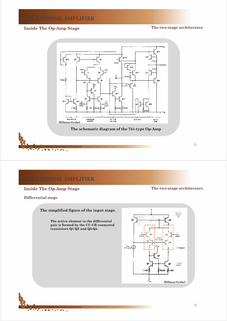
Inside The Op-Amp Stage The two-stage architecture
OPERATIONAL AMPLIFIER
25
The schematic diagram of the 741-type Op-Amp
Millman-Grabel
©Loberg University of Jyväskylä
Inside The Op-Amp Stage
The simplified figure of the input stage.
The active element in the differential
pair is formed by the CC-CB connected
transistors Q1-Q3 and Q2-Q4.
Differential stage
The two-stage architecture
OPERATIONAL AMPLIFIER
26
Millman-Grabel
©Loberg University of Jyväskylä

Inside The Op-Amp Stage
CB-stage
CC-stage
- input+ input
The two-stage architecture
Differential stage
OPERATIONAL AMPLIFIER
27
Input resistance RiCB is emitter
resistance of the CC-stage
6o
4o6o
0
44)CB(i
R
rR1
rR
β
π
++++====
We have to calculate high-resistance active load Ro6 for input resistance of CB-stage.
Millman-Grabel
Millman-Grabel
©Loberg University of Jyväskylä
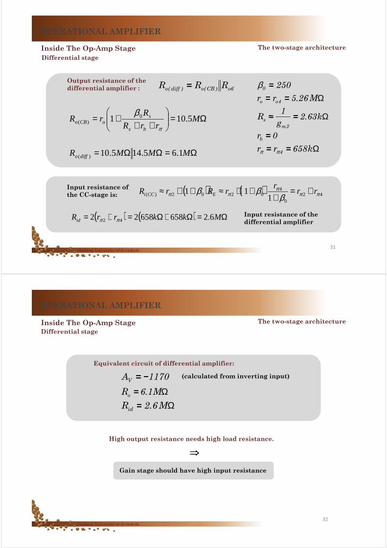
Inside The Op-Amp Stage
ΩΩΩ
ΩΩ M5.14k1k658
k12501M5.10
Rr
R1rR
E6
E06o6o ====
++++⋅⋅⋅⋅++++====
++++++++====
π
β
The two-stage architecture
Differential stage
OPERATIONAL AMPLIFIER
28
Ro6 is output resistance of the
CE-stage with RE
Millman-Grabel
©Loberg University of Jyväskylä

Inside The Op-Amp Stage
Ω
ΩΩΩ
Ωk10
M5.14
M26.5M5.142501
k658
R
rR1
rRR
6o
4o6o
0
4)CC(E4i ≈≈≈≈
++++====
++++========
β
πInput resistance of the
CB-stage :
Loaded voltage gain of the CC-stage :
The two-stage architecture
Differential stage
OPERATIONAL AMPLIFIER
29
(((( ))))(((( ))))
(((( ))))8.0
M5.10k10251k658
M5.10k102501
rR1r
rR1A
2oE02
2oE0
)4Ri,CC(V ≈≈≈≈⋅⋅⋅⋅++++
⋅⋅⋅⋅++++====
⋅⋅⋅⋅++++++++⋅⋅⋅⋅++++
≈≈≈≈ΩΩΩ
ΩΩβ
β
π
Output resistance of
the CC-stage is : Ωk63.2g
1
1
r
1
rrRrR
2m0
2
0
22bs2oTh ====≈≈≈≈
++++≈≈≈≈
++++++++++++====
ββππ
1A )CC(V ≈≈≈≈Unloaded voltage gain of the CC-stage : ∞∞∞∞→→→→ER
©Loberg University of Jyväskylä
Inside The Op-Amp Stage
C
L0
0
is
L)CB(V
R
R1
RR
RA
β
β
++++++++−−−−====
6
46
o
oo
C
L
R
rR
R
R =
C
Li
R
Rr
R
0
4
1 βπ
+≈
where :
And Rs is output resistance
of the CC-stage 2.63kΩ
Voltage gain of the CB-stage
The two-stage architecture
Differential stage
sR
4iR
CB-stageCC-stage
vCCAvCBA
CC-stage
CB-stageQ2
Q4
OPERATIONAL AMPLIFIER
30
1170
R
Rr1
R
Rr1
r
1
r
RrA
6o
6o4o
0
0
6o
6o4o
0
4
0
2
6o04
)CB(V −−−−≈≈≈≈++++
++++++++
++++
−−−−====
β
β
ββππ
ΩM26.5r 4o ====ΩM5.14R 6o ====
2500 ====βΩk658rr 24 ======== ππ
where :
Voltage gain of the diff. Amp
(inverting input) :1170AAA cCBvCCvdif −−−−≈≈≈≈====
©Loberg University of Jyväskylä
CB-stageCC-stage
Inside The Op-Amp Stage
Output resistance of the
differential amplifier : 6o)CB(o)diff(o RRR ====
Ω=
+++= M
rrR
RrR
bs
soCBo 5.101 0
)(π
β
2500 ====βΩM26.5rr 4oo ========
Ωk63.2g
1R
2m
s ====≈≈≈≈
0rb ====
The two-stage architecture
Differential stage
OPERATIONAL AMPLIFIER
31
0rb ====Ωk658rr 4 ======== ππΩ=ΩΩ= MMMR diffo 1.65.145.10)(
( ) ( ) 420
40202)( 1
11 πππ
ππ βββ rr
rrRrR ECCi +=
+++≈++≈Input resistance of
the CC-stage is:
( ) ( ) Ω=Ω+Ω=+= MkkrrRid 6.265865822 42 ππInput resistance of the
differential amplifier
©Loberg University of Jyväskylä
Inside The Op-Amp Stage
Equivalent circuit of differential amplifier:
1170AV −−−−====ΩM1.6Ro ====
ΩM6.2Rid ====
(calculated from inverting input)
The two-stage architecture
Differential stage
OPERATIONAL AMPLIFIER
32
id
High output resistance needs high load resistance.
Gain stage should have high input resistance
⇒⇒⇒⇒
©Loberg University of Jyväskylä

Inside The Op-Amp Stage
Gain stage
The two-stage architecture
OPERATIONAL AMPLIFIER
33
CC-stage CE-stage with
active load
Differential
stage
Millman-Grabel
©Loberg University of Jyväskylä
Inside The Op-Amp Stage
16or
The small-signal
equivalent circuit
of the gain stage.
The two-stage architecture
Gain stage
OPERATIONAL AMPLIFIER
34
2500 ====β0r 16b ====
Ωk391A16
mV25250
I
V
gr
16CQ
T0
16m
016 ====⋅⋅⋅⋅============
µββ
π
ΩM1.6Rs ====Ωk50RE ====
ΩM25.6A16
V100
I
Vr
16C
A16o ============
µ
(((( ))))(((( )))) 66.0
rR1rrR
rR1A
16oE01616bs
16oE0
)CC(V ≈≈≈≈++++++++++++++++
++++====
ββ
π
ΩΩΩ k17k86.25k50
1
rrRrRR
0
1616bs16oE)CC(o
========
++++++++++++====
βπ
Output resistance of CC-stage
Voltage gain of CC-stage
Millman-Grabel
©Loberg University of Jyväskylä

Inside The Op-Amp Stage
Voltage gain of CE-stage 334
R
R1RrrR
RA
C
L0E1717bs
L0)CE(V −−−−====
++++++++++++++++
−−−−====β
β
π
2500 =β0=br
where
Voltage gain of CC-CE-cascade :
The two-stage architecture
Gain stage
OPERATIONAL AMPLIFIER
35
0=br
Ω== kA
Vro 8.181
550
10017 µ
Ω=== kA
VrR BoC 9.90
55050
13 µΩ== krrR BooL 6.601317
Ω== kRR CCos 17)(
Ω== kI
Vr
CQ
T 4.1117
017 βπ
22033466.0)()( −=⋅−=⋅= CEVCCVV AAA
©Loberg University of Jyväskylä
Ωk8.71RrrR
R1rRR
Ebs
E0oC
'
o ====
++++++++++++++++====
π
β
The output resistance of the CC-CE cascade is :2500 =β
0=br
Ω= kro 1.18117
Ω= kr 4.1117π
Ω== kRR CCos 17)(
Ω= 100R
where
Inside The Op-Amp Stage
The two-stage architecture Gain stage
OPERATIONAL AMPLIFIER
36
Ω= 100ER
(((( ))))(((( ))))(((( )))) ΩΩ
Ω
M2.5rk19251r
rRk501rrR
16o16
16oiCE0biCC
≈≈≈≈++++≈≈≈≈
++++++++++++====
π
π β
The input resistance of the CC-CE cascade is :
(((( ))))[[[[ ]]]]Ωk30
RRr
R1rRrrR
EC17o
C017oE17b17iCE ≈≈≈≈
++++++++++++++++++++++++====
βπ
©Loberg University of Jyväskylä

5
OL 106.2A ××××≈≈≈≈Ωk72Ro ≈≈≈≈
Diff Gain
Inside The Op-Amp Stage The two-stage architecture
Gain stage
OPERATIONAL AMPLIFIER
37
1170Adm −−−−≈≈≈≈ 220A CECC −−−−≈≈≈≈−−−−
Ωk72Ro ≈≈≈≈
©Loberg University of Jyväskylä
Inside The Op-Amp Stage
Level Shift
V7.0VVVV −−−−≈≈≈≈−−−−====
The two-stage architecture
OPERATIONAL AMPLIFIER
38
V7.0VVVV IBEIO −−−−≈≈≈≈−−−−====
21
2
RR
R
++++VO is attenuated by
)RIV(VV 1OBEIO ++++−−−−====
)VV(VV ZBEIO ++++−−−−====
Millman-Grabel
©Loberg University of Jyväskylä

Millman-Grabel
Inside The Op-Amp Stage
Voltage Multiplier
The two-stage architecture
Level Shift
OPERATIONAL AMPLIFIER
39
(((( )))) )914(R
R1VRR
R
VV
4
3BE43
4
BE −−−−
++++====++++====
Variable
©Loberg University of Jyväskylä
)1114(1
Rg1
RRgRg1
RgA
41m
432m22m
22mV −−−−≈≈≈≈
++++++++++++++++
≈≈≈≈
Inside The Op-Amp Stage The two-stage architecture
Level Shift
OPERATIONAL AMPLIFIER
40
Millman-Grabel
)1014(R
R2VVV
4
3BEIO −−−−
++++−−−−====
1Rg1 22m0 >>>>>>>>>>>>>>>>β
41m
432
Rg1
RRRsekä
++++++++>>>>>>>>
when

Inside The Op-Amp Stage
The basic Complementary Emitter-follower
Output Stage
The two-stage architecture
OPERATIONAL AMPLIFIER
41
Crossover
distortion
Millman-Grabel
©Loberg University of Jyväskylä
Inside The Op-Amp Stage
Elimination of Crossover distortion
The two-stage architecture
Output Stage
OPERATIONAL AMPLIFIER
42
Millman-Grabel
©Loberg University of Jyväskylä

Inside The Op-Amp Stage
Current
limitersVBE-multiplier Current
limiters
Elimination of Crossover distortion
The two-stage architecture
Output Stage
OPERATIONAL AMPLIFIER
43
Darlington pair
instead of diodes
Millman-Grabel Millman-Grabel
©Loberg University of Jyväskylä
The End of Part 7
OPERATIONAL AMPLIFIER
44
The End of Part 7
©Loberg University of Jyväskylä