Embed Size (px)
Citation preview
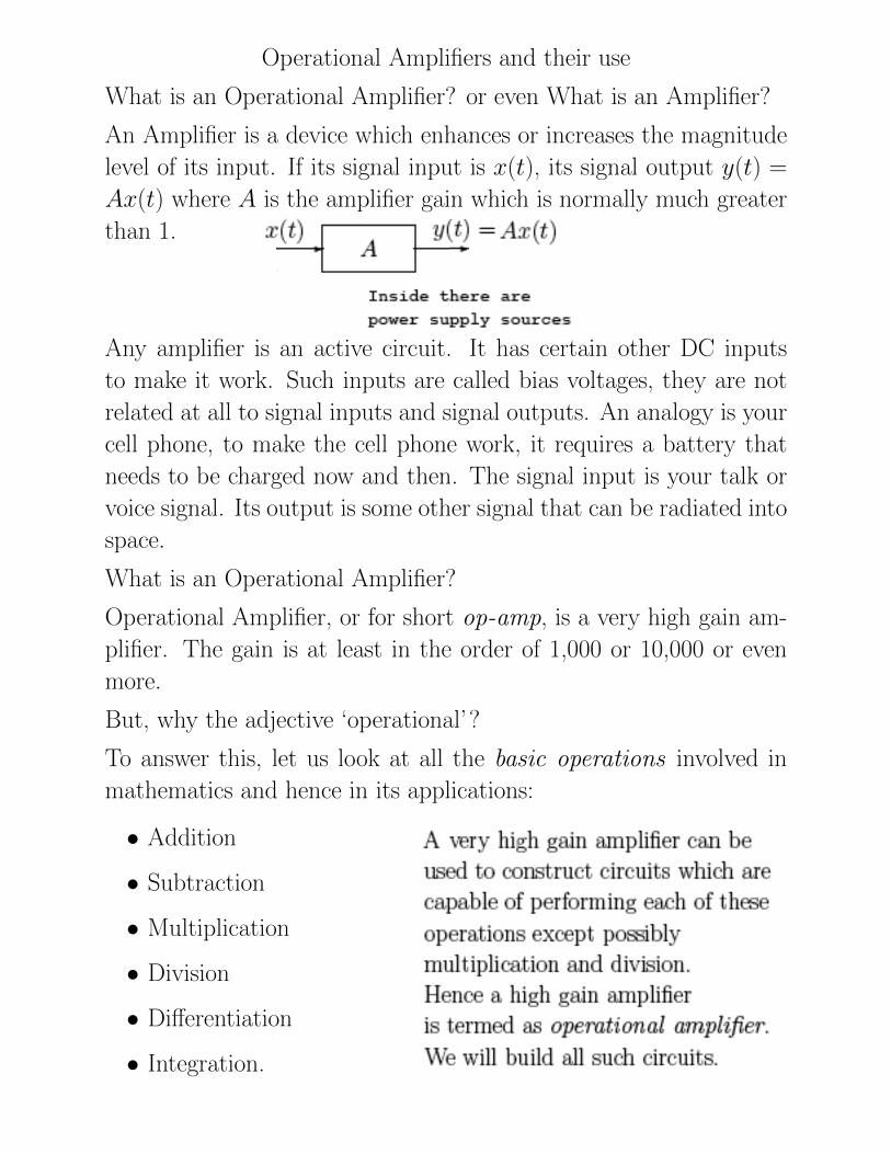
Operational Amplifiers and their use
What is an Operational Amplifier? or even What is an Amplifier?
An Amplifier is a device which enhances or increases the magnitude
level of its input. If its signal input is x(t), its signal output y(t) =
Ax(t) where A is the amplifier gain which is normally much greater
than 1.
Any amplifier is an active circuit. It has certain other DC inputs
to make it work. Such inputs are called bias voltages, they are not
related at all to signal inputs and signal outputs. An analogy is your
cell phone, to make the cell phone work, it requires a battery that
needs to be charged now and then. The signal input is your talk or
voice signal. Its output is some other signal that can be radiated into
space.
What is an Operational Amplifier?
Operational Amplifier, or for short op-amp, is a very high gain am-
plifier. The gain is at least in the order of 1,000 or 10,000 or even
more.
But, why the adjective ‘operational’?
To answer this, let us look at all the basic operations involved in
mathematics and hence in its applications:
• Addition
• Subtraction
• Multiplication
• Division
• Differentiation
• Integration.
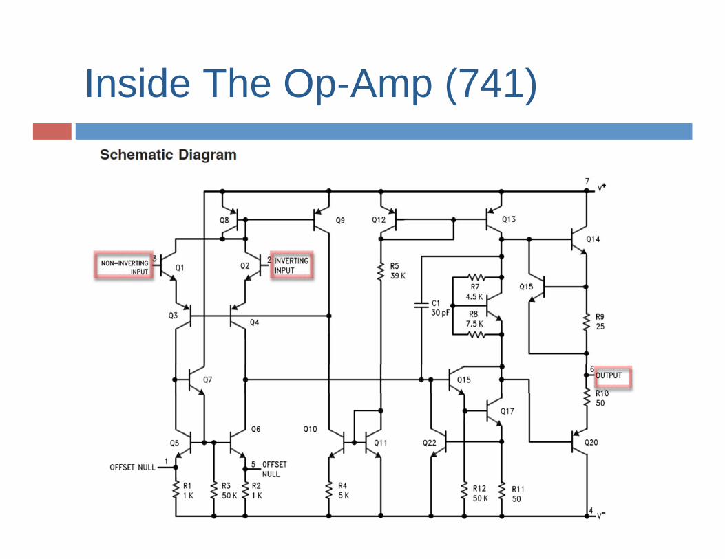
Inside The Op-Amp (741)
Principles of Electrical Engineering I
A Block Diagram with a High-gain Amplifier
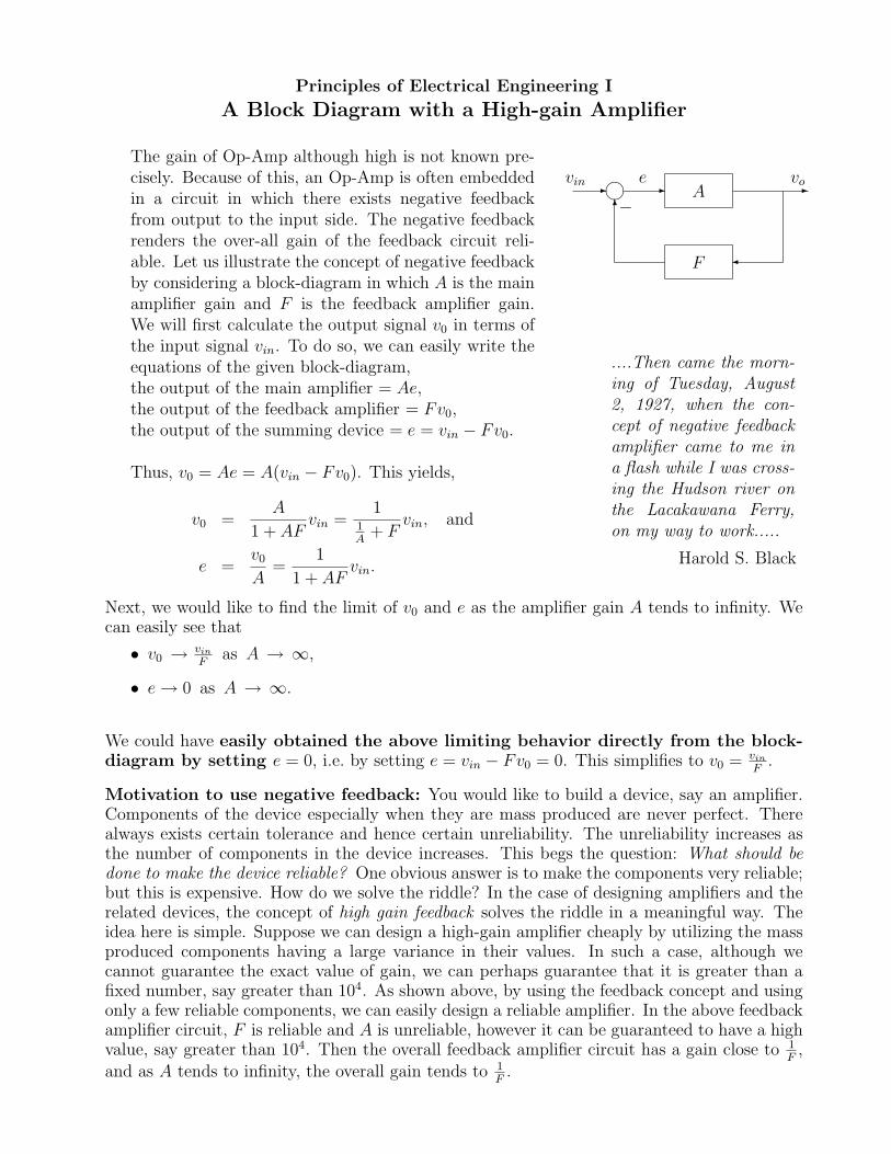
The gain of Op-Amp although high is not known pre-cisely. Because of this, an Op-Amp is often embeddedin a circuit in which there exists negative feedbackfrom output to the input side. The negative feedbackrenders the over-all gain of the feedback circuit reli-able. Let us illustrate the concept of negative feedbackby considering a block-diagram in which A is the mainamplifier gain and F is the feedback amplifier gain.We will first calculate the output signal v0 in terms ofthe input signal vin. To do so, we can easily write theequations of the given block-diagram,the output of the main amplifier = Ae,the output of the feedback amplifier = Fv0,the output of the summing device = e = vin − Fv0.
Thus, v0 = Ae = A(vin − Fv0). This yields,
v0 =A
1 + AFvin =
11A
+ Fvin, and
e =v0
A=
1
1 + AFvin.
A
F
-k−
6
- -vin e vo
....Then came the morn-ing of Tuesday, August2, 1927, when the con-cept of negative feedbackamplifier came to me ina flash while I was cross-ing the Hudson river onthe Lacakawana Ferry,on my way to work.....
Harold S. Black
Next, we would like to find the limit of v0 and e as the amplifier gain A tends to infinity. Wecan easily see that
• v0 → vin
Fas A → ∞,
• e→ 0 as A → ∞.
We could have easily obtained the above limiting behavior directly from the block-diagram by setting e = 0, i.e. by setting e = vin − Fv0 = 0. This simplifies to v0 = vin
F.
Motivation to use negative feedback: You would like to build a device, say an amplifier.Components of the device especially when they are mass produced are never perfect. Therealways exists certain tolerance and hence certain unreliability. The unreliability increases asthe number of components in the device increases. This begs the question: What should bedone to make the device reliable? One obvious answer is to make the components very reliable;but this is expensive. How do we solve the riddle? In the case of designing amplifiers and therelated devices, the concept of high gain feedback solves the riddle in a meaningful way. Theidea here is simple. Suppose we can design a high-gain amplifier cheaply by utilizing the massproduced components having a large variance in their values. In such a case, although wecannot guarantee the exact value of gain, we can perhaps guarantee that it is greater than afixed number, say greater than 104. As shown above, by using the feedback concept and usingonly a few reliable components, we can easily design a reliable amplifier. In the above feedbackamplifier circuit, F is reliable and A is unreliable, however it can be guaranteed to have a highvalue, say greater than 104. Then the overall feedback amplifier circuit has a gain close to 1
F,
and as A tends to infinity, the overall gain tends to 1F.
Principles of Electrical Engineering I
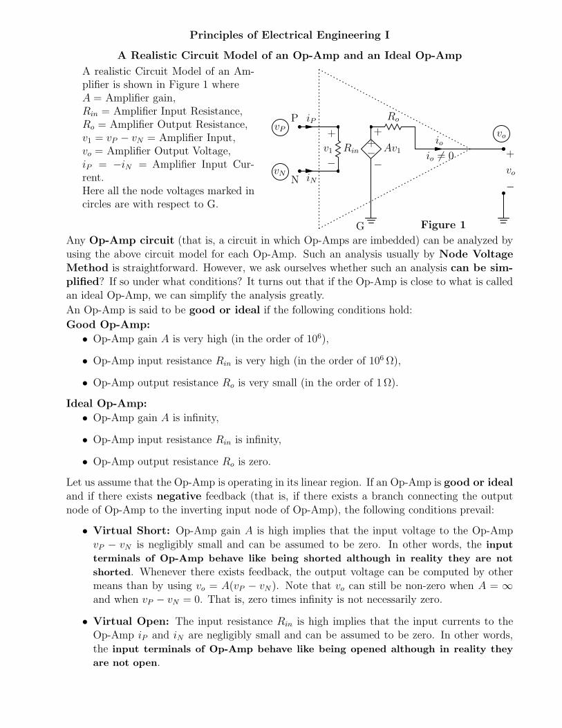
A Realistic Circuit Model of an Op-Amp and an Ideal Op-Amp
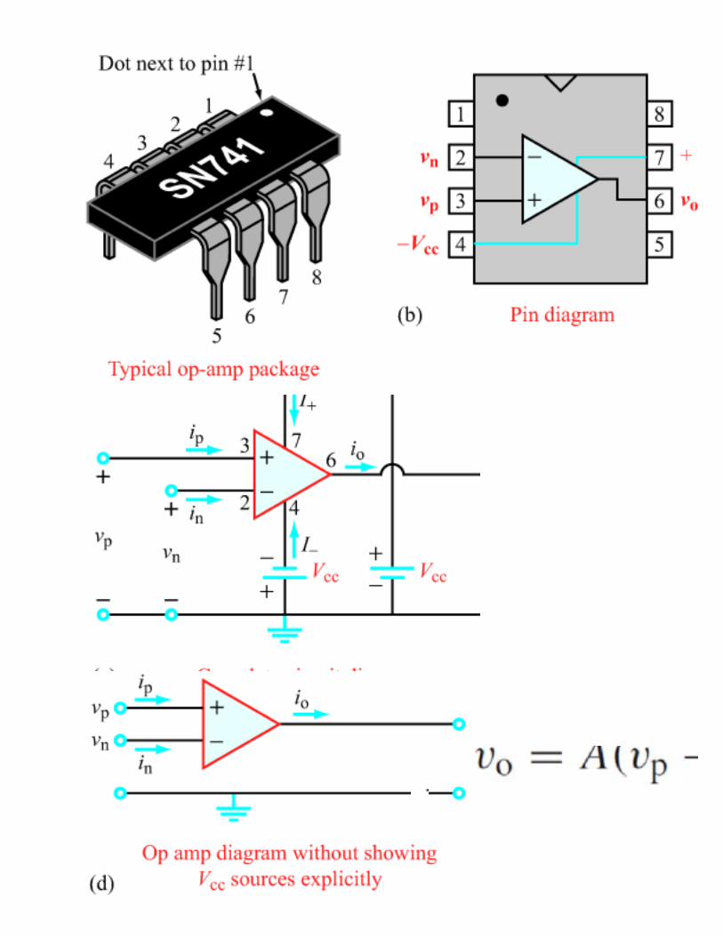
A realistic Circuit Model of an Am-plifier is shown in Figure 1 whereA = Amplifier gain,Rin = Amplifier Input Resistance,Ro = Amplifier Output Resistance,v1 = vP − vN = Amplifier Input,vo = Amplifier Output Voltage,iP = −iN = Amplifier Input Cur-rent.Here all the node voltages marked incircles are with respect to G.
−
v1
+
Rin−
+
−
Av1
+
Ro
G
N
P
−
vo
+
vP
vN
vo
iN
iP
io
io 6= 0
Figure 1
Any Op-Amp circuit (that is, a circuit in which Op-Amps are imbedded) can be analyzed by
using the above circuit model for each Op-Amp. Such an analysis usually by Node Voltage
Method is straightforward. However, we ask ourselves whether such an analysis can be sim-
plified? If so under what conditions? It turns out that if the Op-Amp is close to what is calledan ideal Op-Amp, we can simplify the analysis greatly.
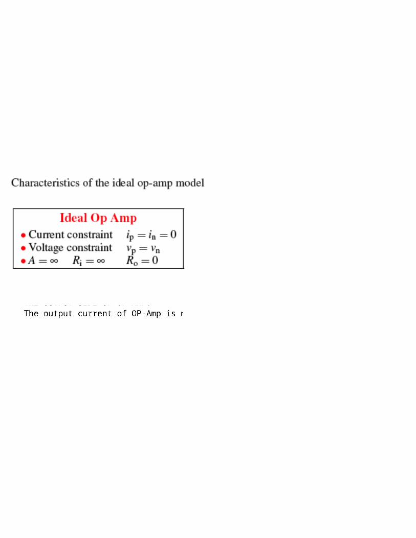
An Op-Amp is said to be good or ideal if the following conditions hold:
Good Op-Amp:
• Op-Amp gain A is very high (in the order of 106),
• Op-Amp input resistance Rin is very high (in the order of 106 Ω),
• Op-Amp output resistance Ro is very small (in the order of 1 Ω).
Ideal Op-Amp:
• Op-Amp gain A is infinity,
• Op-Amp input resistance Rin is infinity,
• Op-Amp output resistance Ro is zero.
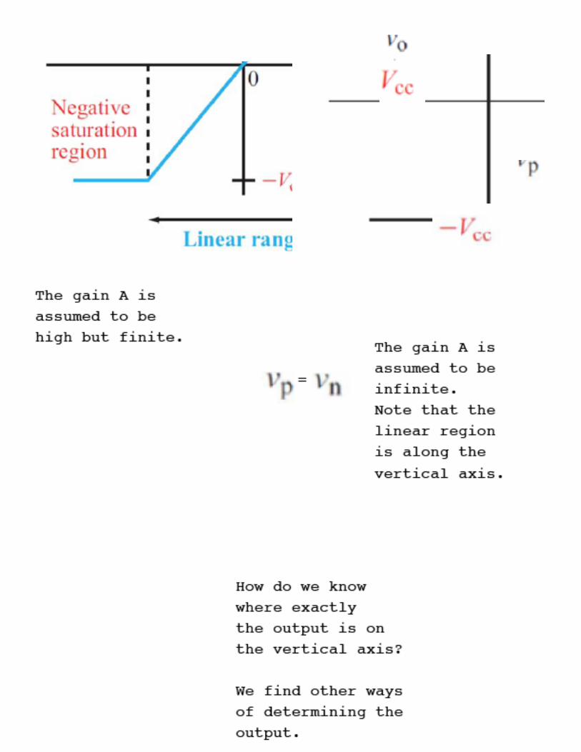
Let us assume that the Op-Amp is operating in its linear region. If an Op-Amp is good or ideal
and if there exists negative feedback (that is, if there exists a branch connecting the output
node of Op-Amp to the inverting input node of Op-Amp), the following conditions prevail:
• Virtual Short: Op-Amp gain A is high implies that the input voltage to the Op-Amp
vP − vN is negligibly small and can be assumed to be zero. In other words, the input
terminals of Op-Amp behave like being shorted although in reality they are not
shorted. Whenever there exists feedback, the output voltage can be computed by other
means than by using vo = A(vP − vN ). Note that vo can still be non-zero when A = ∞
and when vP − vN = 0. That is, zero times infinity is not necessarily zero.
• Virtual Open: The input resistance Rin is high implies that the input currents to theOp-Amp iP and iN are negligibly small and can be assumed to be zero. In other words,
the input terminals of Op-Amp behave like being opened although in reality they
are not open.
2
The concepts of Virtual Short and Virtual Open are very useful in analyzing Op-Amp circuitsas will be illustrated soon. Most of the Op-Amps commercially available can be assumed to
be more or less ideal at least for the initial analysis of an Op-Amp circuit. For more accurateresults one can utilize a more realistic circuit model for the Op-Amp as given in Figure 1. For
even more precision work, there exist other Op-Amp circuit models in the literature.
Important note about io: The output current of Op-Amp is NOT zero. It depends on theload connected to Op-Amp. In view of this, it is always better to analyze circuits by writing
node equations at the input terminals N and P of Op-Amp.
A feel for numbers – What is small? – What is large?
We are going to consider what can be called ideal Op-amps. To understandsome of the assumptions we make in this regard, you need to have a feel fornumbers, in particular what is small and what is large when compared tosomething else. Without comparison between numbers, nothing can be saidto be small and nothing can be said to be large.Let us first understand the following:
• The highest possible output of an Op-amp is Vcc which is of the orderof 4 to 24 volts as prescribed by the manufacturer.
• All signals in an Op-amp circuit are at the most in the order of Vcc,some of the signals are much smaller than Vcc and thus are negligiblein comparison with Vcc.
• When Op-amp gain is large, the linear region of its input-output char-acteristic is small.
To get a feel for numbers, let us consider an equation where A is large andis in the order of 107 and x, y and z are at the most 10,
Ax + y = z ⇒ x =z − y
A.
We note that x tends to zero as A tends to infinity. Another way of sayingthe same is, x is negligible in comparison with z − y, or z − y is large incomparison with x.
Let us look at one of the equations of ‘non-inverting’ Op-amp circuit,
vo − vnR1
+vo − A(vp − vn)
Ro
= 0.
This can be re-written as
A(vp − vn) =Ro
R1
(vo − vn) + v0 ⇒ vp − vn =Ro
R1(vo − vn) + v0
A.
The right hand side of the right equation tends to zero as A tends to infinity.This implies that for a large A, vp − vn is small in comparison with othersignals. For A =∞, we have vp− vn = 0, that is vp = vn. The input currentip = vp−vn
Riis also small when vp − vn is small.
The above discussion implies that for the ‘non-inverting’ Op-amp circuitwe have considered, the input to the Op-amp, namely vp − vn, is small ornegligible. Also, input current ip to the Op-amp is small or negligible as well.In general, whenever the output of Op-amp is fed back to its input side, wehave
• input voltage to Op-amp is negligible (virtual open).
• input current to Op-amp is negligible (virtual short).
Summary
• When does life begin?your choice: → at conception, at birth, when you get driver license
• When does EE life begin?there is only one choice: → when you learn circuit analysis and logic design
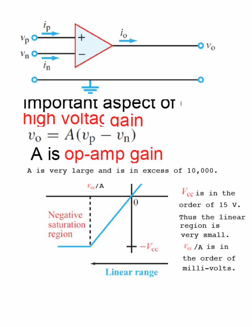
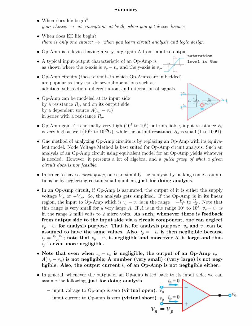
• Op-Amp is a device having a very large gain A from input to output.
• A typical input-output characteristic of an Op-Amp isas shown where the x-axis is vp − vn and the y-axis is vo.
• Op-Amp circuits (those circuits in which Op-Amps are imbedded)are popular as they can do several operations such as:addition, subtraction, differentiation, and integration of signals.
• Op-Amp can be modeled at its input sideby a resistance Ri, and on its output sideby a dependent source A(vp − vn)in series with a resistance Ro.
• Op-Amp gain A is normally very high (104 to 108) but unreliable, input resistance Ri
is very high as well (1010 to 1013Ω), while the output resistance Ro is small (1 to 100Ω).
• One method of analyzing Op-Amp circuits is by replacing an Op-Amp with its equiva-lent model. Node Voltage Method is best suited for Op-Amp circuit analysis. Such ananalysis of an Op-Amp circuit using equivalent model for an Op-Amp yields whateveris needed. However, it presents a lot of algebra, and a quick grasp of what a givencircuit does is not feasible.
• In order to have a quick grasp, one can simplify the analysis by making some assump-tions or by neglecting certain small numbers, just for doing analysis.
• In an Op-Amp circuit, if Op-Amp is saturated, the output of it is either the supplyvoltage Vcc or −Vcc. So, the analysis gets simplified. If the Op-Amp is in its linearregion, the input to Op-Amp which is vp − vn is in the range −Vcc
Ato Vcc
A. Note that
this range is very small for a very large A. If A is in the range 104 to 108, vp − vn isin the range 2 milli volts to 2 micro volts. As such, whenever there is feedbackfrom output side to the input side via a circuit component, one can neglectvp − vn for analysis purpose. That is, for analysis purpose, vp and vn can beassumed to have the same values. Also, ip = −in is then negligible becauseip = vp−vn
Ri; note that vp − vn is negligible and moreover Ri is large and thus
ip is even more negligible.
• Note that even when vp − vn is negligible, the output of an Op-Amp vo =A(vp − vn) is not negligible; A number (very small)×(very large) is not neg-ligible. Also, the output current io of an Op-Amp is not negligible either.
• In general, whenever the output of an Op-amp is fed back to its input side, we canassume the following, just for doing analysis.
– input voltage to Op-amp is zero (virtual open).
– input current to Op-amp is zero (virtual short).
Principles of Electrical Engineering I
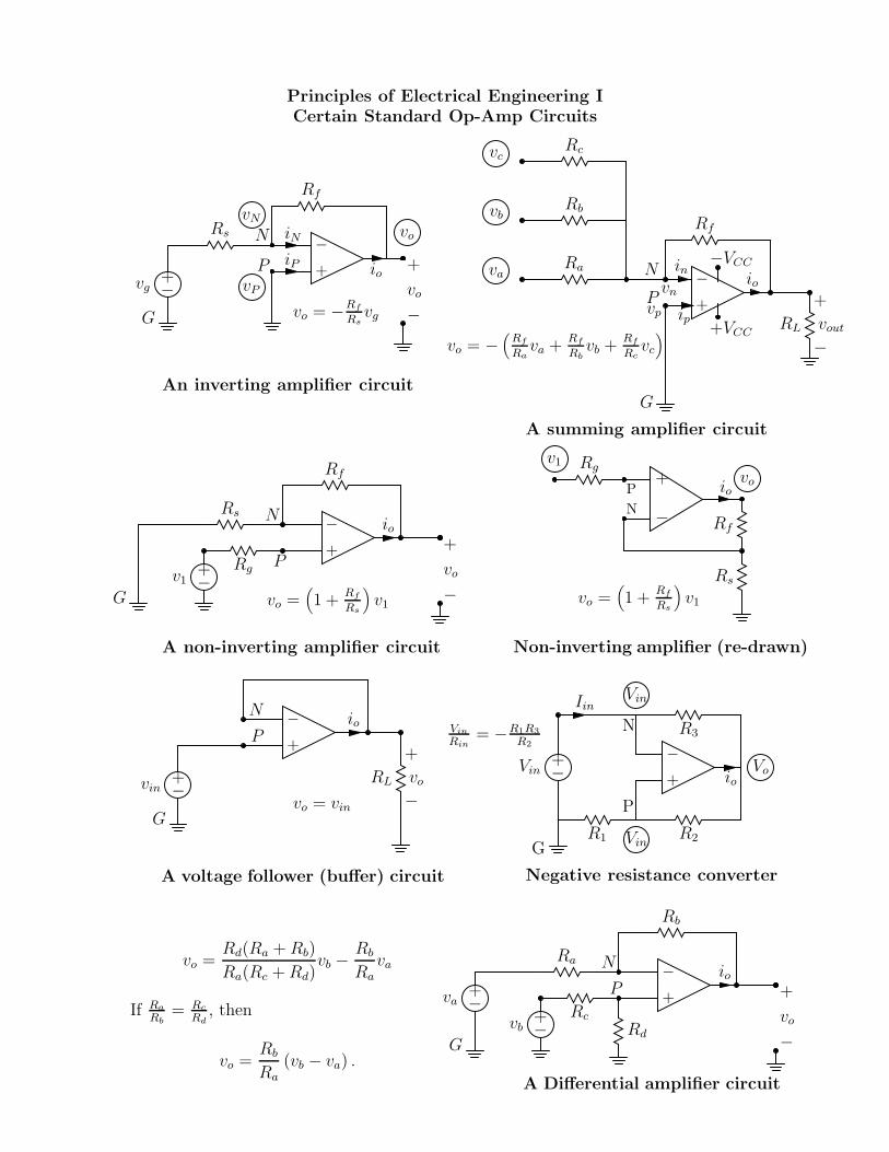
Certain Standard Op-Amp Circuits
−
+vg
Rs−
+
Rf
N
P
G −
vo
+vP
vN
voiN
iP io
vo = −Rf
Rsvg
An inverting amplifier circuit
vaRa
Rbvb
−
+
G
Rf
RL
+
vout
−
N
P
−VCC
+VCC
vn
in
vp ip
io
Rcvc
vo = −
(
Rf
Rava +
Rf
Rb
vb +Rf
Rcvc
)
A summing amplifier circuit
Rs−
+
Rg
−
+v1
Rf
+
vo
−
N
P
G
io
vo =(
1 +Rf
Rs
)
v1
A non-inverting amplifier circuit
io
−
+P
N
Rg
Rf
Rs
v1
vo
vo =(
1 +Rf
Rs
)
v1
Non-inverting amplifier (re-drawn)
−
+vin
−
+
N
P
G−
vo
+
RL
io
vo = vin
A voltage follower (buffer) circuit
−
+
R3
R2R1
−
+Vin
G
Iin
N
P
Vin
Vin
Voio
Vin
Rin
= −R1R3
R2
Negative resistance converter
vo =Rd(Ra + Rb)
Ra(Rc + Rd)vb −
Rb
Ra
va
If Ra
Rb
= Rc
Rd
, then
vo =Rb
Ra
(vb − va) .
−
+va
Ra−
+
Rc
−
+vb
Rb
+
vo
−
N
P
G
io
Rd
A Differential amplifier circuit
Principles of Electrical Engineering I
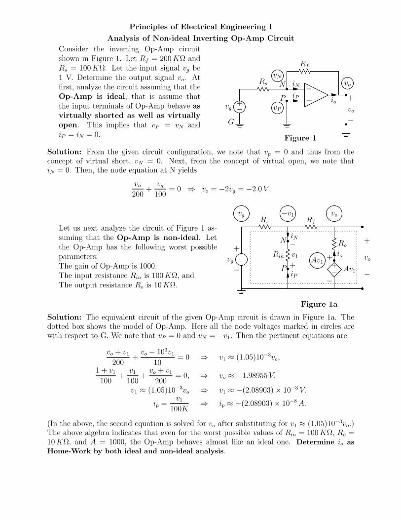
Analysis of Non-ideal Inverting Op-Amp Circuit
Consider the inverting Op-Amp circuitshown in Figure 1. Let Rf = 200 KΩ andRs = 100 KΩ. Let the input signal vg be1 V. Determine the output signal vo. Atfirst, analyze the circuit assuming that theOp-Amp is ideal, that is assume thatthe input terminals of Op-Amp behave as
virtually shorted as well as virtually
open. This implies that vP = vN andiP = iN = 0.
−
+vg
Rs−
+
Rf
N
P
G −
vo
+vP
vN
voiN
iP io
Figure 1
Solution: From the given circuit configuration, we note that vp = 0 and thus from theconcept of virtual short, vN = 0. Next, from the concept of virtual open, we note thatiN = 0. Then, the node equation at N yields
vo
200+
vg
100= 0 ⇒ vo = −2vg = −2.0 V.
Let us next analyze the circuit of Figure 1 as-suming that the Op-Amp is non-ideal. Letthe Op-Amp has the following worst possibleparameters:The gain of Op-Amp is 1000,The input resistance Rin is 100 KΩ, andThe output resistance Ro is 10 KΩ.
−
vg
+
vgRs
−v1
Rf
vo
Ro
Av1
−
+
−
+
Av1
Rin
+
v1
−N
P−
vo
+iN
iP
io
Figure 1a
Solution: The equivalent circuit of the given Op-Amp circuit is drawn in Figure 1a. Thedotted box shows the model of Op-Amp. Here all the node voltages marked in circles arewith respect to G. We note that vP = 0 and vN = −v1. Then the pertinent equations are
vo + v1
200+
vo − 103v1
10= 0 ⇒ v1 ≈ (1.05)10−3vo,
1 + v1
100+
v1
100+
vo + v1
200= 0, ⇒ vo ≈ −1.98955 V,
v1 ≈ (1.05)10−3vo ⇒ v1 ≈ −(2.08903) × 10−3 V.
ip =v1
100K⇒ ip ≈ −(2.08903) × 10−8 A.
(In the above, the second equation is solved for vo after substituting for v1 ≈ (1.05)10−3vo.)The above algebra indicates that even for the worst possible values of Rin = 100 KΩ, Ro =10 KΩ, and A = 1000, the Op-Amp behaves almost like an ideal one. Determine io as
Home-Work by both ideal and non-ideal analysis.
332:221 Principles of Electrical Engineering I
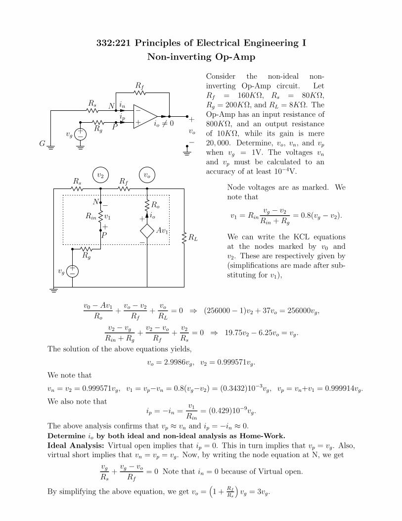
Non-inverting Op-Amp
Rs−
+
Rg
−
+vg
Rf
+
vo
−
N
P
G
ip
in
io 6= 0
Consider the non-ideal non-inverting Op-Amp circuit. LetRf = 160KΩ, Rs = 80KΩ,Rg = 200KΩ, and RL = 8KΩ. TheOp-Amp has an input resistance of800KΩ, and an output resistanceof 10KΩ, while its gain is mere20, 000. Determine, vo, vn, and vp
when vg = 1V. The voltages vn
and vp must be calculated to anaccuracy of at least 10−4V.
Rs
v2
Rf
vo
RL
Ro
+
−
Av1
Rg
−
+vg
Rin
+
v1
−N
P
io
Node voltages are as marked. Wenote that
v1 = Rin
vg − v2
Rin + Rg
= 0.8(vg − v2).
We can write the KCL equationsat the nodes marked by v0 andv2. These are respectively given by(simplifications are made after sub-stituting for v1),
v0 − Av1
Ro
+vo − v2
Rf
+vo
RL
= 0 ⇒ (256000 − 1)v2 + 37vo = 256000vg,
v2 − vg
Rin + Rg
+v2 − vo
Rf
+v2
Rs
= 0 ⇒ 19.75v2 − 6.25vo = vg.
The solution of the above equations yields,
vo = 2.9986vg, v2 = 0.999571vg.
We note that
vn = v2 = 0.999571vg, v1 = vp−vn = 0.8(vg−v2) = (0.3432)10−3vg, vp = vn+v1 = 0.999914vg.
We also note thatip = −in =
v1
Rin
= (0.429)10−9vg.
The above analysis confirms that vp ≈ vn and ip = −in ≈ 0.
Determine io by both ideal and non-ideal analysis as Home-Work.
Ideal Analysis: Virtual open implies that ip = 0. This in turn implies that vp = vg. Also,virtual short implies that vn = vp = vg. Now, by writing the node equation at N, we get
vg
Rs
+vg − vo
Rf
= 0 Note that in = 0 because of Virtual open.
By simplifying the above equation, we get vo =(
1 +Rf
Rs
)
vg = 3vg.
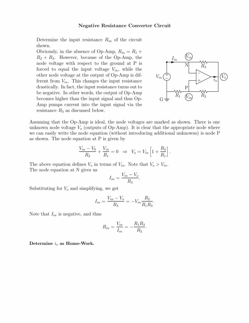
Negative Resistance Converter Circuit
Determine the input resistance Rin of the circuitshown.Obviously, in the absence of Op-Amp, Rin = R1 +R2 + R3. However, because of the Op-Amp, thenode voltage with respect to the ground at P isforced to equal the input voltage Vin, while theother node voltage at the output of Op-Amp is dif-ferent from Vin. This changes the input resistancedrastically. In fact, the input resistance turns out tobe negative. In other words, the output of Op-Ampbecomes higher than the input signal and thus Op-Amp pumps current into the input signal via theresistance R3 as discussed below.
−
+
R3
R2R1
−
+Vin
G
Iin
N
P
Vin
Vin
Voio
Assuming that the Op-Amp is ideal, the node voltages are marked as shown. There is oneunknown node voltage Vo (outputs of Op-Amp). It is clear that the appropriate node wherewe can easily write the node equation (without introducing additional unknowns) is node Pas shown. The node equation at P is given by
Vin − V0
R2
+Vin
R1
= 0 ⇒ Vo = Vin
[
1 +R2
R1
]
.
The above equation defines Vo in terms of Vin. Note that Vo > Vin.The node equation at N gives us
Iin =Vin − Vo
R3
.
Substituting for Vo and simplifying, we get
Iin =Vin − Vo
R3
= −Vin
R2
R1R3
.
Note that Iin is negative, and thus
Rin =Vin
Iin
= −R1R3
R2
.
Determine io as Home-Work.
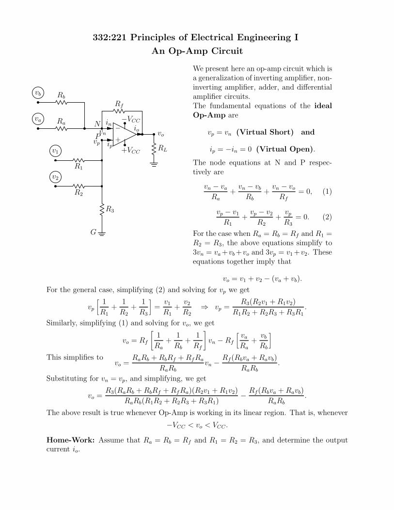
332:221 Principles of Electrical Engineering I
An Op-Amp Circuit
va Ra
Rbvb
−
+
R1
v1
R2
v2
R3
G
vo
Rf
RL
N
P
−VCC
+VCC
vn
in
vp ip
io
We present here an op-amp circuit which isa generalization of inverting amplifier, non-inverting amplifier, adder, and differentialamplifier circuits.The fundamental equations of the ideal
Op-Amp are
vp = vn (Virtual Short) and
ip = −in = 0 (Virtual Open).
The node equations at N and P respec-tively are
vn − va
Ra
+vn − vb
Rb
+vn − vo
Rf
= 0, (1)
vp − v1
R1
+vp − v2
R2
+vp
R3
= 0. (2)
For the case when Ra = Rb = Rf and R1 =R2 = R3, the above equations simplify to3vn = va +vb +vo and 3vp = v1 +v2. Theseequations together imply that
vo = v1 + v2 − (va + vb).
For the general case, simplifying (2) and solving for vp we get
vp
[
1
R1
+1
R2
+1
R3
]
=v1
R1
+v2
R2
⇒ vp =R3(R2v1 + R1v2)
R1R2 + R2R3 + R3R1
.
Similarly, simplifying (1) and solving for vo, we get
vo = Rf
[
1
Ra
+1
Rb
+1
Rf
]
vn − Rf
[
va
Ra
+vb
Rb
]
This simplifies tovo =
RaRb + RbRf + RfRa
RaRb
vn −Rf(Rbva + Ravb)
RaRb
.
Substituting for vn = vp, and simplifying, we get
vo =R3(RaRb + RbRf + RfRa)(R2v1 + R1v2)
RaRb(R1R2 + R2R3 + R3R1)−
Rf(Rbva + Ravb)
RaRb
.
The above result is true whenever Op-Amp is working in its linear region. That is, whenever
−VCC < vo < VCC .
Home-Work: Assume that Ra = Rb = Rf and R1 = R2 = R3, and determine the outputcurrent io.
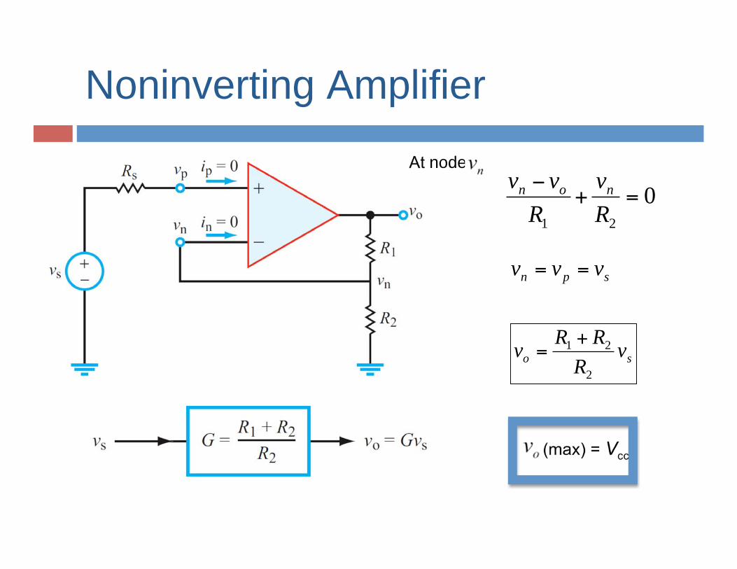
Noninverting Amplifier
0
21
=+R
v
R
vvnon
sov
R
RRv
2
21+
=
spnvvv ==
(max) = Vcc
At node
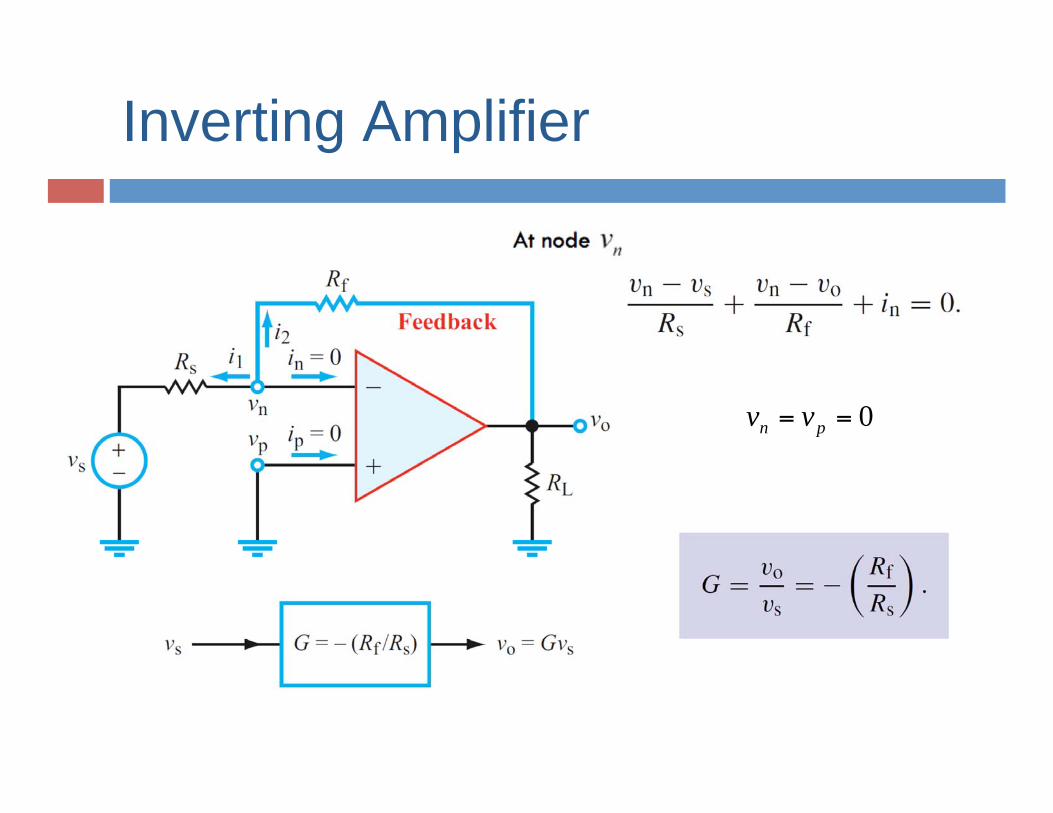
Inverting Amplifier
0==pn
vv
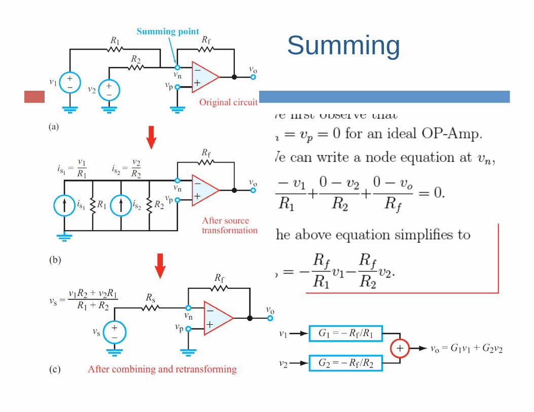
Summing
Amplifier
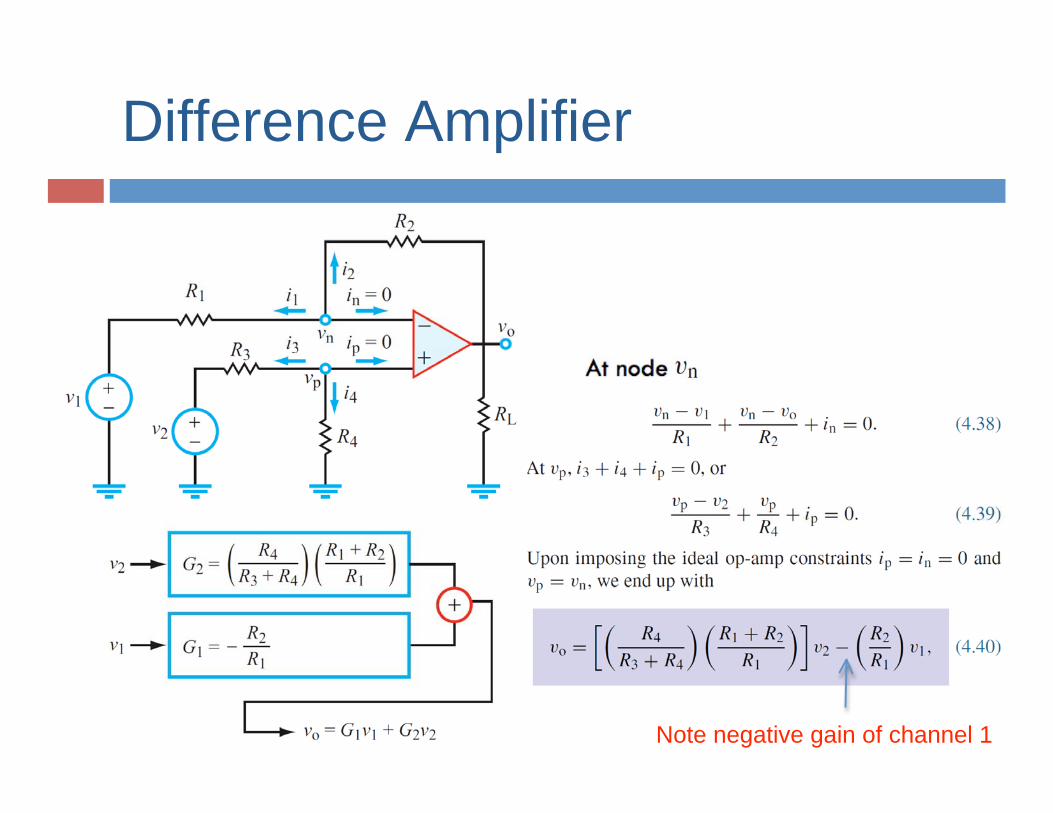
Difference Amplifier
Note negative gain of channel 1
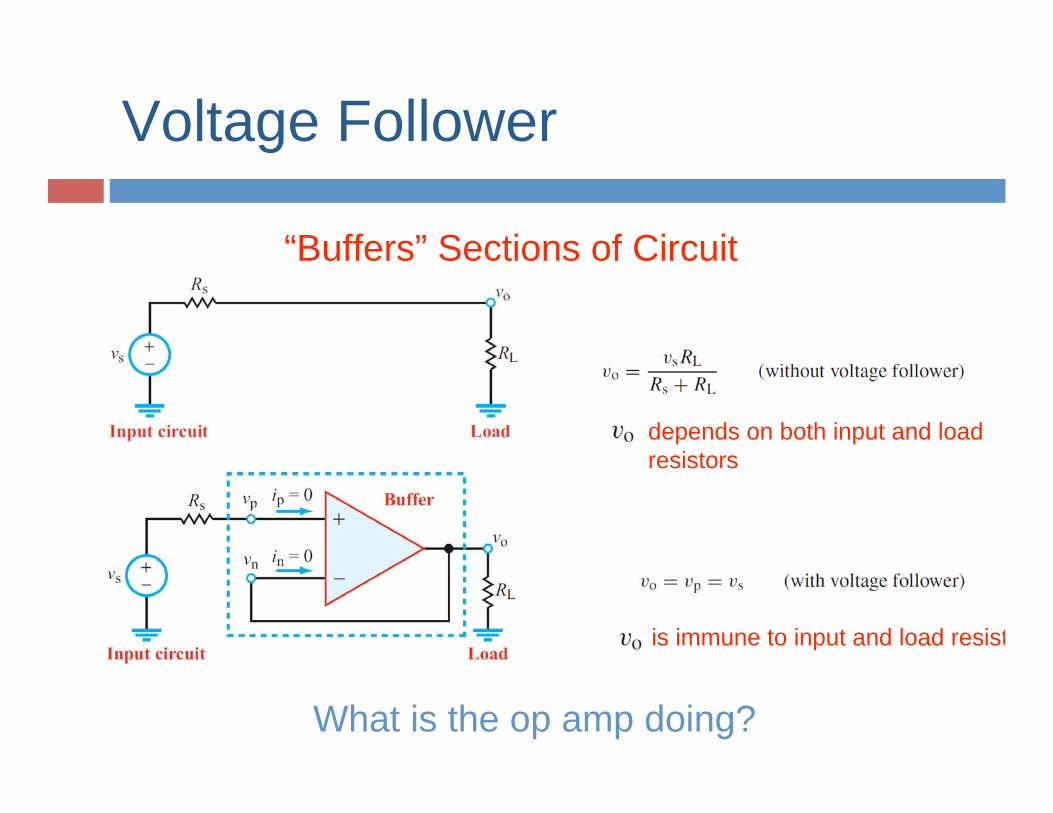
Voltage Follower
“Buffers” Sections of Circuit
What is the op amp doing?
depends on both input and load
resistors
is immune to input and load resist
Principles of Electrical Engineering I
Quiz Fall 1999
Student’s name in capital letters:
Last four digits of SSN:
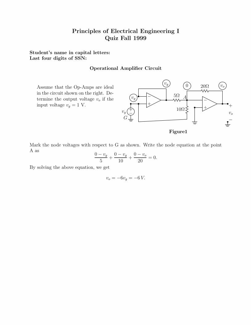
Operational Amplifier Circuit
Assume that the Op-Amps are idealin the circuit shown on the right. De-termine the output voltage vo if theinput voltage vg = 1 V.
−
+vg
−
+
5Ω−
++
vo
−
20Ω
10Ω
G
Avg
vg 0 vo
Figure1
Mark the node voltages with respect to G as shown. Write the node equation at the pointA as
0 − vg
5+
0 − vg
10+
0 − vo
20= 0.
By solving the above equation, we get
vo = −6vg = −6 V.
Principles of Electrical Engineering I
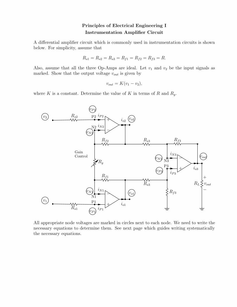
Instrumentation Amplifier Circuit
A differential amplifier circuit which is commonly used in instrumentation circuits is shownbelow. For simplicity, assume that
Rs1 = Rs2 = Rs3 = Rf1 = Rf2 = Rf3 = R.
Also, assume that all the three Op-Amps are ideal. Let v1 and v2 be the input signals asmarked. Show that the output voltage vout is given by
vout = K(v1 − v2),
where K is a constant. Determine the value of K in terms of R and Rg.
io1
iN1
iP1
+
−N1
P1
vN1
vP1
vo1
Rf1
io2
iN2
iP2
+
−N2
P2
vN2
vP2
vo2
Rf2
Rg
Gain
Control
Rs1
Rs2
v1
v2
Rs3
Rs3
Rf3
io3
iN3
iP3
+
−N3
P3
Rf3
RL
+
vout
−
voutvN3
vP3
All appropriate node voltages are marked in circles next to each node. We need to write thenecessary equations to determine them. See next page which guides writing systematicallythe necessary equations.
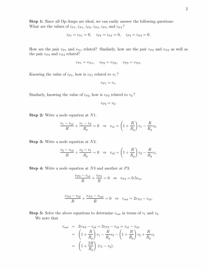
2
Step 1: Since all Op-Amps are ideal, we can easily answer the following questions:What are the values of iP1, iN1, iP2, iN2, iP3, and iN3 ?
iP1 = iN1 = 0, iP2 = iN2 = 0, iP3 = iN3 = 0.
How are the pair vP1 and vN1 related? Similarly, how are the pair vP2 and vN2 as well asthe pair vP3 and vN3 related?
vP1 = vN1, vP2 = vN2, vP3 = vN3.
Knowing the value of iP1, how is vP1 related to v1 ?
vP1 = v1.
Similarly, knowing the value of iP2, how is vP2 related to v2 ?
vP2 = v2.
Step 2: Write a node equation at N1.
v1 − vo1
R+
v1 − v2
Rg
= 0 ⇒ vo1 =
(
1 +R
Rg
)
v1 −R
Rg
v2.
Step 3: Write a node equation at N2.
v2 − vo2
R+
v2 − v1
Rg
= 0 ⇒ vo2 =
(
1 +R
Rg
)
v2 −R
Rg
v1.
Step 4: Write a node equation at N3 and another at P3.
vP3 − vo1
R+
vP3
R= 0 ⇒ vP3 = 0.5vo1.
vN3 − vo2
R+
vN3 − vout
R= 0 ⇒ vout = 2vN3 − vo2.
Step 5: Solve the above equations to determine vout in terms of v1 and v2.
We note that
vout = 2vN3 − vo2 = 2vP3 − vo2 = vo1 − vo2
=
(
1 +R
Rg
)
v1 −R
Rg
v2 −
(
1 +R
Rg
)
v2 +R
Rg
v1
=
(
1 +2R
Rg
)
(v1 − v2) .

HW from Nilsson and Riedel 8th and 9th editions
Nilsson and Riedel 8th edition:
5.2, 5.5, 5.18, 5.25
Nilsson and Riedel 9th edition:
5.3, 5.6, 5.18, 5.28
Name in CAPITAL LETTERS: HW: DAC with Op-AmpLAST FOUR DIGITS OF ID NUMBER:
332:221 Principles of Electrical Engineering I
Theme Example – DAC– loading effect removed by adding an op-amp circuit:HW, collected and graded
G
−
+
−
v1
+
−
+
−
v2
+
−
+
−
v3
+
−
+
−
v4
+RL
−
vout
+2R2R2R2R
2R
R R R a
gg4 g3 g2 g1
e d c b a
The above DAC circuit with load has a problem. The output voltage vout depends on theload RL. To reduce the effect of load, we can add an inverting op-amp circuit as shownbelow.
G
−
+
−
v1
+
−
+
−
v2
+
−
+
−
v3
+
−
+
−
v4
+
2R2R2R2R
2R
R R R a
gg4 g3 g2 g1
e d c b a
io+
−
N
P
Rf
RL
−
vout
+
Assuming that the op-amp is ideal, determine the feedback resistance Rf in terms of R suchthat the output voltage vout is given by
vout = −8v1 − 4v2 − 2v3 − v4.
Hint: The Thevenin equivalent of the DAC circuit to the left of terminals ‘a’ and ‘g’ is givenby
vTh = 1
2v1 + 1
4v2 + 1
8v3 + 1
16v4,
andRTh = R.
Name in CAPITAL LETTERS:
LAST FOUR DIGITS OF ID NUMBER:
HW: Summing Circuit
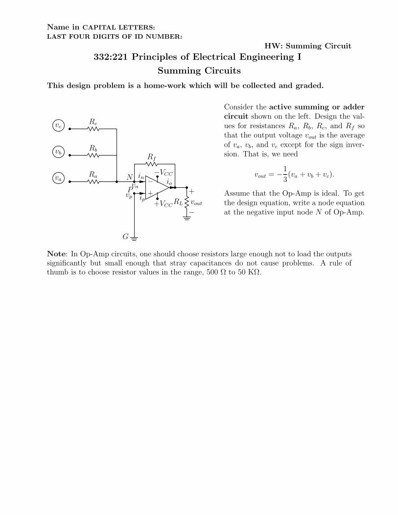
332:221 Principles of Electrical Engineering I
Summing Circuits
This design problem is a home-work which will be collected and graded.
vaRa
Rbvb
−
+
G
Rf
RL
+
vout
−
N
P
−VCC
+VCC
vn
in
vp ip
io
Rcvc
Consider the active summing or adder
circuit shown on the left. Design the val-ues for resistances Ra, Rb, Rc, and Rf sothat the output voltage vout is the averageof va, vb, and vc except for the sign inver-sion. That is, we need
vout = −1
3(va + vb + vc).
Assume that the Op-Amp is ideal. To getthe design equation, write a node equationat the negative input node N of Op-Amp.
Note: In Op-Amp circuits, one should choose resistors large enough not to load the outputssignificantly but small enough that stray capacitances do not cause problems. A rule ofthumb is to choose resistor values in the range, 500 Ω to 50 KΩ.
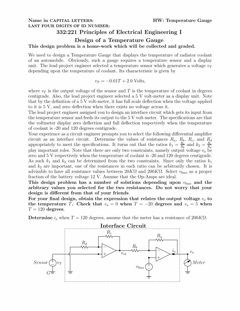
Name in CAPITAL LETTERS: HW: Temperature GaugeLAST FOUR DIGITS OF ID NUMBER:
332:221 Principles of Electrical Engineering I
Design of a Temperature GaugeThis design problem is a home-work which will be collected and graded.
We need to design a Temperature Gauge that displays the temperature of radiator coolantof an automobile. Obviously, such a gauge requires a temperature sensor and a displayunit. The lead project engineer selected a temperature sensor which generates a voltage vT
depending upon the temperature of coolant. Its characteristic is given by
vT = −0.01T + 2.0 Volts,
where vT is the output voltage of the sensor and T is the temperature of coolant in degreescentigrade. Also, the lead project engineer selected a 5 V volt-meter as a display unit. Notethat by the definition of a 5 V volt-meter, it has full scale deflection when the voltage appliedto it is 5 V, and zero deflection when there exists no voltage across it.The lead project engineer assigned you to design an interface circuit which gets its input fromthe temperature sensor and feeds its output to the 5 V volt-meter. The specifications are thatthe voltmeter display zero deflection and full deflection respectively when the temperatureof coolant is -20 and 120 degrees centigrade.Your experience as a circuit engineer prompts you to select the following differential amplifiercircuit as an interface circuit. Determine the values of resistances Ra, Rb, Rc, and Rd
appropriately to meet the specifications. It turns out that the ratios k1 = Ra
Rb
and k2 = Rc
Rd
play important roles. Note that there are only two constraints, namely output voltage vo bezero and 5 V respectively when the temperature of coolant is -20 and 120 degrees centigrade.As such k1 and k2 can be determined from the two constraints. Since only the ratios k1
and k2 are important, one of the resistances in each ratio can be arbitrarily chosen. It isadvisable to have all resistance values between 20KΩ and 200KΩ. Select vbias as a properfraction of the battery voltage 12 V. Assume that the Op-Amps are ideal.This design problem has a number of solutions depending upon vbias and thearbitrary values you selected for the two resistances. Do not worry that yourdesign is different from that of your friends.For your final design, obtain the expression that relates the output voltage vo tothe temperature T . Check that vo = 0 when T = −20 degrees and vo = 5 whenT = 120 degrees.
Determine io when T = 120 degrees, assume that the meter has a resistance of 200KΩ.
Interface Circuit
Rd−
+
−
+ vTSensor
Rc
G
Rb−
+
−
+vbias
Ra
Meter
iovo1vo
2
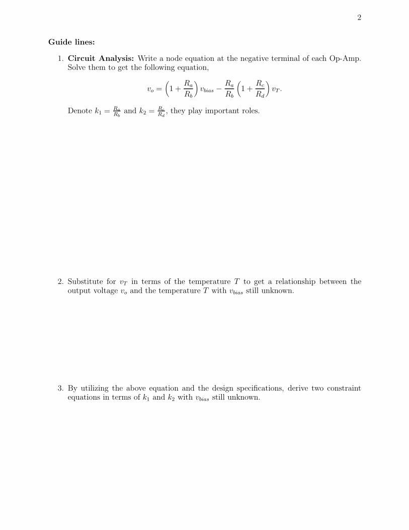
Guide lines:
1. Circuit Analysis: Write a node equation at the negative terminal of each Op-Amp.Solve them to get the following equation,
vo =(
1 +Ra
Rb
)
vbias −Ra
Rb
(
1 +Rc
Rd
)
vT .
Denote k1 = Ra
Rb
and k2 = Rc
Rd
, they play important roles.
2. Substitute for vT in terms of the temperature T to get a relationship between theoutput voltage vo and the temperature T with vbias still unknown.
3. By utilizing the above equation and the design specifications, derive two constraintequations in terms of k1 and k2 with vbias still unknown.
3
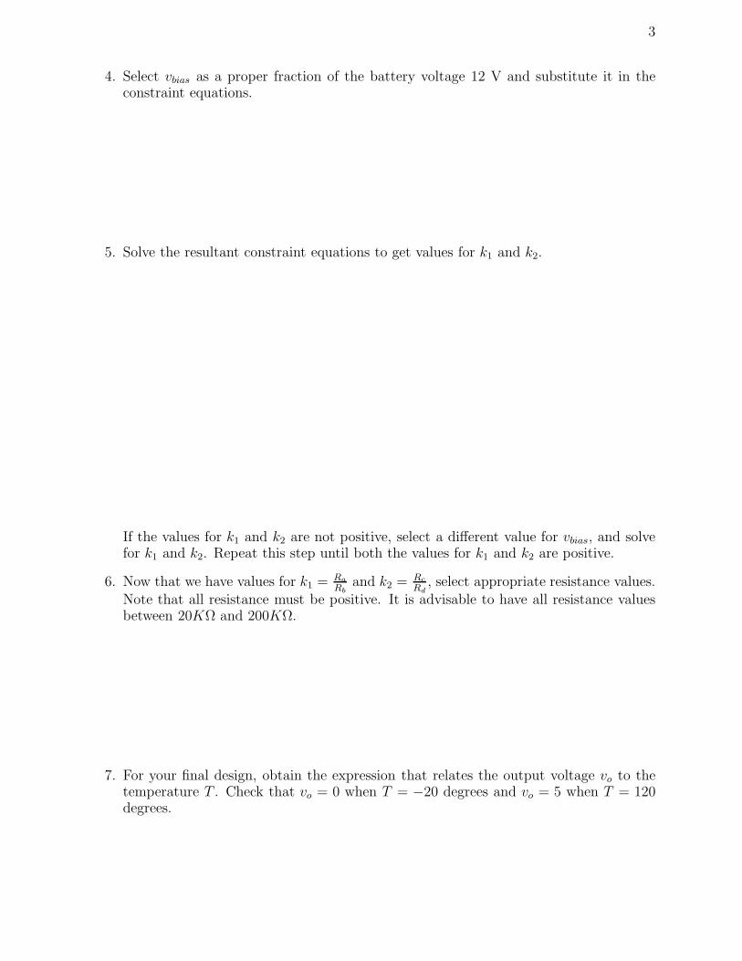
4. Select vbias as a proper fraction of the battery voltage 12 V and substitute it in theconstraint equations.
5. Solve the resultant constraint equations to get values for k1 and k2.
If the values for k1 and k2 are not positive, select a different value for vbias, and solvefor k1 and k2. Repeat this step until both the values for k1 and k2 are positive.
6. Now that we have values for k1 = Ra
Rb
and k2 = Rc
Rd
, select appropriate resistance values.Note that all resistance must be positive. It is advisable to have all resistance valuesbetween 20KΩ and 200KΩ.
7. For your final design, obtain the expression that relates the output voltage vo to thetemperature T . Check that vo = 0 when T = −20 degrees and vo = 5 when T = 120degrees.