Embed Size (px)
Citation preview

Operation of a titanium nitride superconducting microresonator detector in thenonlinear regimeL. J. Swenson, P. K. Day, B. H. Eom, H. G. Leduc, N. Llombart, C. M. McKenney, O. Noroozian, and J.
Zmuidzinas
Citation: Journal of Applied Physics 113, 104501 (2013); doi: 10.1063/1.4794808 View online: http://dx.doi.org/10.1063/1.4794808 View Table of Contents: http://scitation.aip.org/content/aip/journal/jap/113/10?ver=pdfcov Published by the AIP Publishing Articles you may be interested in Suspended plate microresonators with high quality factor for the operation in liquids Appl. Phys. Lett. 104, 191906 (2014); 10.1063/1.4875910 Design and fabrication of a CMOS-compatible MHP gas sensor AIP Advances 4, 031339 (2014); 10.1063/1.4869616 NbTiN superconducting nanowire detectors for visible and telecom wavelengths single photon counting on Si3N4photonic circuits Appl. Phys. Lett. 102, 051101 (2013); 10.1063/1.4788931 Cantilever anemometer based on a superconducting micro-resonator: Application to superfluid turbulence Rev. Sci. Instrum. 83, 125002 (2012); 10.1063/1.4770119 Titanium nitride films for ultrasensitive microresonator detectors Appl. Phys. Lett. 97, 102509 (2010); 10.1063/1.3480420
[This article is copyrighted as indicated in the article. Reuse of AIP content is subject to the terms at: http://scitation.aip.org/termsconditions. Downloaded to ] IP:
131.215.10.13 On: Fri, 23 May 2014 19:12:34
Operation of a titanium nitride superconducting microresonator detectorin the nonlinear regime
L. J. Swenson,1,2,a) P. K. Day,2 B. H. Eom,1 H. G. Leduc,2 N. Llombart,3 C. M. McKenney,1
O. Noroozian,4 and J. Zmuidzinas1,2
1Division of Physics, Mathematics, and Astronomy, California Institute of Technology, Pasadena,California 91125, USA2Jet Propulsion Laboratory, California Institute of Technology, Pasadena, California 91109, USA3Delft University of Technology, 2628 CD Delft, The Netherlands4Quantum Sensors Group, National Institute of Standards and Technology, Boulder, Colorado 80305, USA
(Received 26 November 2012; accepted 22 February 2013; published online 8 March 2013)
If driven sufficiently strongly, superconducting microresonators exhibit nonlinear behavior
including response bifurcation. This behavior can arise from a variety of physical mechanisms
including heating effects, grain boundaries or weak links, vortex penetration, or through the
intrinsic nonlinearity of the kinetic inductance. Although microresonators used for photon
detection are usually driven fairly hard in order to optimize their sensitivity, most experiments to
date have not explored detector performance beyond the onset of bifurcation. Here, we present
measurements of a lumped-element superconducting microresonator designed for use as a far-
infrared detector and operated deep into the nonlinear regime. The 1 GHz resonator was fabricated
from a 22 nm thick titanium nitride film with a critical temperature of 2 K and a normal-state
resistivity of 100 lX cm. We measured the response of the device when illuminated with 6.4 pW
optical loading using microwave readout powers that ranged from the low-power, linear regime
to 18 dB beyond the onset of bifurcation. Over this entire range, the nonlinear behavior
is well described by a nonlinear kinetic inductance. The best noise-equivalent power of
2� 10�16 W=Hz1=2 at 10 Hz was measured at the highest readout power, and represents a �10 fold
improvement compared with operating below the onset of bifurcation. VC 2013 American Institute ofPhysics. [http://dx.doi.org/10.1063/1.4794808]
I. INTRODUCTION
Superconducting detector arrays have a wide range of
applications in physics and astrophysics.1,2 Although the de-
velopment of multiplexed readouts has allowed array sizes to
grow rapidly over the past decade, there is a strong demand
for even larger arrays. For example, current astronomical sub-
millimeter cameras feature arrays with up to 104 pixels.3 In
comparison, the proposed Cerro Chajnantor Atacama
Telescope (CCAT) 25-meter submillimeter telescope4 would
require more than 106 pixels in order to fully sample the focal
plane at a wavelength of k ¼ 350 lm. Another example is
cryogenic dark matter searches which currently implement
arrays with <50 pixels. Each pixel features an integrated
transition-edge sensor (TES) to detect athermal phonons for
�100–500 g of cryogenic detection mass.5,6 Proposed ton-
scale searches would require of order 104 detectors. In order
to meet these challenging scaling requirements, it is highly de-
sirable to simplify detector fabrication and to increase multi-
plexing factors in order to reduce system cost. From this
perspective, superconducting microresonator detectors7–12 are
particularly attractive. In these devices, the energy to be
detected is coupled to a superconducting film, causing Cooper
pairs to be broken into individual electrons or quasiparticles,
which leads to a perturbation of the complex ac conductivity
drðxÞ ¼ dr1 � jdr2. Very sensitive measurements of drðxÞ
may be made if the film is patterned to form a microwave reso-
nant circuit. Because both the amplitude and phase of the com-
plex transmission of the circuit can be measured (see Fig. 1),
information on both the dissipative (dr1) and reactive (dr2)
perturbations may be obtained simultaneously, giving the user a
choice of using reactive readout, dissipation readout, or both.
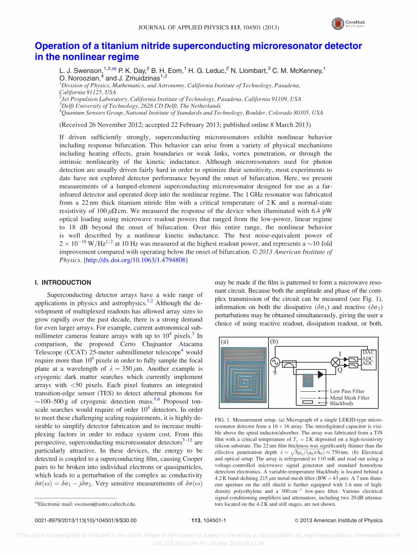
FIG. 1. Measurement setup. (a) Micrograph of a single LEKID-type micro-
resonator detector from a 16� 16 array. The interdigitated capacitor is visi-
ble above the spiral inductor/absorber. The array was fabricated from a TiN
film with a critical temperature of Tc ¼ 2 K deposited on a high-resistivity
silicon substrate. The 22 nm film thickness was significantly thinner than the
effective penetration depth k ¼ffiffiffiffiffiffiffiffiffiffiffiffiffiffiffiffiffiffiffiffiffiffiffiffiffiffi�hqn=ðl0pD0Þ
p� 750 nm. (b) Electrical
and optical setup. The array is refrigerated to 110 mK and read out using a
voltage-controlled microwave signal generator and standard homodyne
detection electronics. A variable-temperature blackbody is located behind a
4.2 K band-defining 215 lm metal-mesh filter (BW¼ 43 lm). A 7 mm diam-
eter aperture on the still shield is further equipped with 1.6 mm of high-
density polyethylene and a 300 cm�1 low-pass filter. Various electrical
signal-conditioning amplifiers and attenuators, including two 20 dB attenua-
tors located on the 4.2 K and still stages, are not shown.a)Electronic mail: [email protected].
0021-8979/2013/113(10)/104501/9/$30.00 VC 2013 American Institute of Physics113, 104501-1
JOURNAL OF APPLIED PHYSICS 113, 104501 (2013)
[This article is copyrighted as indicated in the article. Reuse of AIP content is subject to the terms at: http://scitation.aip.org/termsconditions. Downloaded to ] IP:
131.215.10.13 On: Fri, 23 May 2014 19:12:34

Frequency multiplexing of a detector array is readily accom-
plished by designing each microresonator to have a different
resonant frequency and coupling all of the detectors to a single
transmission line for excitation and readout.
Although various options exist for coupling pair-
breaking photons or phonons into the superconductor, the
simplest approach for a number of applications is to directly
illuminate the microresonator. For good performance, the
resonator must be designed to be an efficient absorber. A
particularly notable example is the structure introduced by
Doyle et al. for far-infrared detection, known as the lumped-
element kinetic inductance detector or LEKID.13,14 Fig. 1(a)
shows a variant of this concept, designed for low interpixel
crosstalk and polarization-insensitive operation.15 The struc-
ture consists of a coplanar stripline spiral inductor and an
interdigitated capacitor. The microwave current density in
the inductor is considerably larger than in the capacitor, so
the inductor is the photosensitive portion of the device. The
resonant frequency can be tuned simply by varying the ge-
ometry of the capacitor or inductor during the array design.
Further, only a single lithography step is necessary for patter-
ing an array of resonators from a superconducting thin-film
deposited on an insulating substrate. The simplicity of these
devices has led to the demonstration of prototype arrays suit-
able for submillimeter astronomy.16 Similar devices have
been developed for optical astronomy17 and dark matter
detection experiments.18,19
Because the pixel size is comparable to the far-infrared
wavelength, the details of the resonator geometry do not
strongly affect the absorption of radiation. However, in order
to achieve high absorption efficiency, the effective far-
infrared surface resistance of the structure should be around
Reff ¼ 377 X=ð1þ ffiffiffiffi�rp Þ � 86 X when using a silicon sub-
strate with dielectric constant �r � 11:5. This results in an
approximate constraint on the sheet resistance Rs and area
filling factor gA of the superconducting film, Reff � Rs=gA,
which is straightforward to satisfy if a high-resistivity super-
conductor such as TiN is used.20 These considerations
provide a starting point for pixel design; detailed electromag-
netic simulations may then be used to optimize the absorp-
tion. TiN is a particularly suitable material for resonator
detectors due to its high intrinsic quality Qi which can
exceed 106 and a tunable Tc based on the nitrogen content
(0 < Tc < 4:7 K).
In practice, superconducting microresonators exhibit
excess frequency noise.7,8,11,21 This noise is due to capaci-
tance fluctuations22 caused by two-level tunneling systems
that are known to be present in amorphous dielectrics.23,24
Such material is clearly present when deposited dielectric
films are used in the resonator capacitor.25 However, experi-
ments have shown that even when the capacitor consists of a
patterned superconducting film on a high-quality crystalline
dielectric substrate, a thin surface layer of amorphous dielec-
tric material is still present and causes excess dissipation and
noise.26,27 This two-level system (TLS) noise has been stud-
ied extensively and a number of techniques have been devel-
oped to reduce it.22,28,29 One of the simplest ways to mitigate
the effects of TLS noise and simultaneously overcome am-
plifier noise is to drive the resonator with the largest readout
power possible.21 This technique is ultimately limited by the
nonlinear response of the resonator. Potential sources of non-
linearity in thin-film superconducting resonators include a
power-dependent current distribution;30 quasiparticle pro-
duction from absorption of readout photons;31 or the nonlin-
ear kinetic inductance intrinsic to superconductivity.32–34
Virtually all measurements of microresonator detectors
reported to date have used a readout power below the onset
of bifurcation. Here, we demonstrate operation of a lumped-
element microresonator detector both in the low-power,
linear regime, and deep in the nonlinear regime well above
the onset of bifurcation. For most of our measurements, the
pixel was illuminated with a substantial optical load of
Popt ¼ 6:4 pW. For comparison, at the highest achievable
readout power (discussed below) the readout power dissi-
pated in the resonator was �1.6 pW. While this is compara-
ble to the optical loading, the efficiency for conversion of
this power into quasiparticles is expected and observed35 to
be low since the energy of each readout photon is a factor of
D=hfr ¼ 1:76kBTc=hfr ¼ 73 below the superconducting gap
energy. Much of the dissipated microwave power may be
expected to escape as low-energy, non-pair-breaking pho-
nons, in which case the quasiparticle population may not
change substantially due to the microwave dissipation. As a
result, it is perhaps not entirely surprising that the behavior
of our device even deep into the bifurcation regime is well
described by a model that includes only the nonlinearity of
the kinetic inductance.
II. THEORETICAL MODEL AND RESONANCE FITTING
The basic principles of superconducting microresonator
detector readout when operating in the linear regime have
been extensively described.7,8 The homodyne readout used
for this measurement is shown in Fig. 1(b). A microresonator
with an intrinsic, unloaded quality factor Qi and, resonance
frequency xr ¼ 1=ffiffiffiffiffiffiLCp
is coupled to a transmission line,
yielding a coupling quality factor Qc. A fraction a of the total
inductance L is contributed by the kinetic inductance Lk such
that Lk ¼ aL. The overall loaded quality factor is given by
Q�1r ¼ Q�1
i þ Q�1c . A signal generator is used to drive the
resonator near its resonance frequency. The transmitted sig-
nal is amplified by a cryogenic amplifier with noise tempera-
ture Tn¼ 6 K, mixed with a copy of the original signal and
digitized. The resulting complex amplitude of the measured
signal is described by the forward transfer function
S21 ¼ 1� Qr
Qc
1
1þ 2jQrx; (1)
where
x ¼ xg � xr
xr(2)
is the fractional detuning of the readout generator frequency
xg relative to the resonance frequency xr. Varying x by
sweeping the generator frequency traces out a circle in the
complex S21 plane. At resonance (xg ¼ xr; x ¼ 0), the circle
crosses the real axis at the closest approach to the origin,
104501-2 Swenson et al. J. Appl. Phys. 113, 104501 (2013)
[This article is copyrighted as indicated in the article. Reuse of AIP content is subject to the terms at: http://scitation.aip.org/termsconditions. Downloaded to ] IP:
131.215.10.13 On: Fri, 23 May 2014 19:12:34

while the S21 values for all generator frequencies far from
resonance fall on the real axis near unity.
Increasing, the readout power results in the onset of non-
linear behavior. As discussed, the most relevant source of
nonlinearity for this device is the nonlinear kinetic induct-
ance of the superconducting film. A power-dependent kinetic
inductance can be written in terms of the resonator current Iwith the expression
LkðIÞ ¼ Lkð0Þ½1þ I2=I2� þ…�; (3)
where odd terms are excluded due to symmetry considera-
tions and I� sets the scaling of the effect. Lkð0Þ is the kinetic
inductance of the resonator in the low-power and linear
limit.
The nonlinear kinetic inductance gives rise to classic
soft-spring Duffing oscillator dynamics.36 In order to quanti-
tatively account for the power-dependent behavior, it is nec-
essary to replace Eq. (1) with a transfer function which takes
into account the resonance shift dxr due to the nonlinear ki-
netic inductance in Eq. (3). The shifted resonance is given by
xr ¼ xr;0 þ dxr, where xr;0 is the low-power resonance fre-
quency. Substituting into Eq. (2), the generator detuning
becomes
x ¼ xg � xr;0 � dxr
xr;0 � dxr� x0 � dx; (4)
where the approximation is calculated to first order and
x0 ¼xg � xr;0
xr;0(5)
is the detuning in the low-power and linear limit. At a stored
resonator energy E, the nonlinear frequency shift dx is
given by
dx ¼ dxr
xr;0¼ � 1
2
dL
L¼ � a
2
I2
I2�¼ � E
E�; (6)
where the scaling energy E� / LkI2�=a
2 is expected to be of
order the condensation energy of the inductor if a � 1.
To proceed further, an expression for the stored resona-
tor energy at a given readout power and frequency is
required. The available generator power Pg can be reflected
back to the generator, transmitted past the resonator, or dissi-
pated in the resonator. Conservation of power can be
expressed by
Pdiss ¼ Pg½1� jS11j2 � jS21j2�; (7)
where Pdiss is the power dissipated in the resonator and S11 is
the normalized amplitude of the reflected wave. Noting that
S11 ¼ S21 � 1 for a shunt-coupled circuit and substituting
Eq. (1) into Eq. (7) yields the result
Pdiss ¼ Pg2Q2
r
QiQc
1
1þ 4Q2r x2
� �: (8)
Using the standard definition of the internal quality factor
Qi ¼xrE
Pdiss
; (9)
the resonator energy is found to be
E ¼ 2Q2r
Qc
1
1þ 4Q2r x2
Pg
xr: (10)
Equation (4) is an implicit equation for the power-
shifted detuning x as a function of the generator power Pg
and detuning at low power, x0. To see this, recall from Eqs.
(4) and (6) that x ¼ x0 þ E=E�. Combining this with Eq. (10)
yields
x ¼ x0 þ2Q2
r
Qc
1
1þ 4Q2r x2
Pg
xrE�: (11)
Introducing, the variables y ¼ Qrx and y0 ¼ Qrx0 as well as
the nonlinearity parameter
a ¼ 2Q3r
Qc
Pg
xrE�(12)
allows Eq. (11) to be rewritten as
y ¼ y0 þa
1þ 4y2: (13)
Using the definition of the quality factor Qr ¼ xr=Dx,
where Dx is the linewidth of the resonance, we see that
y ¼ Qrx ¼ ðxg � xrÞ=Dx. Thus, y and y0 are the generator
detuning measured in linewidths relative to the power-
shifted resonance and the low-power resonance, respectively.
Solutions to Eq. (13) for a range of a are shown in Fig. 2. As
can be seen from this plot, y becomes nonmonotonic with y0
for a > 4ffiffiffi3p
=9 � 0:8.
FIG. 2. Solutions to Eq. (13) for a range of the nonlinear parameter a. The
solid (dashed) arrows indicate downward (upward) frequency sweeping. The
horizontal scale y0 is the generator detuning measured relative to the low-
power resonance frequency xr;0. The vertical scale is the generator detuning
y measured relative to the shifted resonance frequency xr . For a > 4ffiffiffi3p
=9
� 0:8, y is nonmonotonic in y0.
104501-3 Swenson et al. J. Appl. Phys. 113, 104501 (2013)
[This article is copyrighted as indicated in the article. Reuse of AIP content is subject to the terms at: http://scitation.aip.org/termsconditions. Downloaded to ] IP:
131.215.10.13 On: Fri, 23 May 2014 19:12:34
The origin of the bifurcation is conceptually simple to
understand and is visualized in Fig. 3. If the generator fre-
quency is swept upwards starting from below the resonance,
the resonator current increases as the detuning decreases,
and the nonlinear inductance causes the resonance to shift
downward toward the generator frequency, reducing the
detuning further. This process eventually results in a run-
away positive feedback condition as the resonator “snaps”
into the energized state. In contrast, sweeping downwards
from the high-frequency side results in negative feedback as
the resonance also shifts downwards, away from the genera-
tor tone. The generator tone chases the resonance downward
until sweeping past the resonance minimum when the reso-
nator abruptly snaps back to its non-energized state. The
maximum frequency shift during downward frequency
sweeping will depend on the readout power and reflects the
I2 dependence of the kinetic inductance in Eq. (3). Notice
that smooth downward frequency sweeping allows access to
the entire high-frequency side of the resonance.
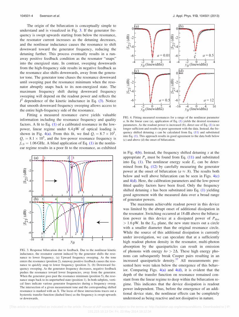
Fitting a measured resonance curve yields valuable
information including the resonance frequency and quality
factors. A fit to Eq. (1) of a calibrated resonance in the low-
power, linear regime under 6.4 pW of optical loading is
shown in Fig. 4(a). From this fit, we find Qi ¼ 8:7� 105;Qc ¼ 8:1� 105, and the low-power resonance frequency is
fr;0 ¼ 1:06 GHz. A blind application of Eq. (1) in the nonlin-
ear regime results in a poor fit to the resonance, as exhibited
in Fig. 4(b). Instead, the frequency shifted detuning x at the
appropriate Pg must be found from Eq. (11) and substituted
into Eq. (1). The nonlinear energy scale E� can be deter-
mined from Eq. (12) by carefully measuring the generator
power at the onset of bifurcation (a � :8). The results both
below and well above bifurcation can be seen in Figs. 4(c)
and 4(d). Here, the calibration parameters and the low-power
fitted quality factors have been fixed. Only the frequency
shifted detuning x has been substituted into Eq. (1) yielding
good agreement with the measured data over a broad range
of generator powers.
The maximum achievable readout power in this device
was limited by the abrupt onset of additional dissipation in
the resonator. Switching occurred at 18 dB above the bifurca-
tion power in this device at a dissipated power of Pdiss
> 1:6 pW. In the S21 plane, the new state traces out a circle
with a smaller diameter than the original resonance circle.
While the source of this additional dissipation is currently
under investigation, we can speculate that at a sufficiently
high readout photon density in the resonator, multi-photon
absorption by the quasiparticles can result in emission
of phonons with energy h� > 2D. These high energy pho-
nons can subsequently break Cooper pairs resulting in an
increased quasiparticle density.37 All measurements pre-
sented here were taken below the emergence of this behav-
ior. Comparing Figs. 4(a) and 4(d), it is evident that the
depth of the transfer function on resonance remained con-
stant from the linear regime to deep within the bifurcation re-
gime. This indicates that the device dissipation is readout
power independent. Thus, before the emergence of an addi-
tional device state, the nonlinear effects can be completely
understood as being reactive and not dissipative in nature.
FIG. 3. Response bifurcation due to feedback. Due to the nonlinear kinetic
inductance, the resonator current induced by the generator shifts the reso-
nance to lower frequency. (a) Upward frequency sweeping. As the tone
enters the resonance (position 2), runaway positive feedback causes the reso-
nance to quickly snap to lower frequency (position 3). (b) Downward fre-
quency sweeping. As the generator frequency decreases, negative feedback
pushes the resonance toward lower frequencies, away from the generator.
When the generator goes past the resonance minimum (position 5), the reso-
nance snaps back to its unperturbed state (position 1). In both subplots, verti-
cal lines indicate various generator frequencies during a frequency sweep.
The intersection of a given measurement tone and the corresponding shifted
resonance is marked with an X. The locus of these intersections traces out a
hysteretic transfer function (dashed lines) as the frequency is swept upwards
or downwards.
FIG. 4. Fitting measured resonances for a range of the nonlinear parameter
a. In the linear case (a), application of Eq. (1) yields the desired resonance
parameters. As the readout power is increased (b), direct use of Eq. (1) is no
longer sufficient and results in poor agreement with the data. Instead, the fre-
quency shifted detuning x can be calculated from Eq. (11) and substituted
into Eq. (1). This approach results in good agreement to the data both below
(c) and above (d) the onset of bifurcation.
104501-4 Swenson et al. J. Appl. Phys. 113, 104501 (2013)
[This article is copyrighted as indicated in the article. Reuse of AIP content is subject to the terms at: http://scitation.aip.org/termsconditions. Downloaded to ] IP:
131.215.10.13 On: Fri, 23 May 2014 19:12:34

The condensation energy of the inductor is given by
Econd ¼ N0D2VL=2, where N0 is the single spin density of
states at the Fermi energy, D � 3:5kBTc=2 is the supercon-
ducting gap, and VL is the volume of the inductor.38 Econd
¼ 3� 10�13 J for this device. This is a factor of 5 greater
than the energy scale E� determined from the onset of bifur-
cation. Additional measurements of resonator detectors sug-
gest E� and Econd are comparable for a variety of inductor
volumes and critical temperatures.39,40 While Econd and E�are in reasonably good agreement, caution must be exercised
when comparing these quantities, because knowledge of the
absolute power level at the resonator is difficult to ascertain.
This uncertainty arises from the changing electrical attenua-
tion of the microwave coaxial cable upon cooling and, in
particular, impedance mismatch between the 50 X coaxial
transmission line and the on-chip coplanar waveguide.
Additionally, the superconducting gap D is current dependent
and deviates from the zero current value near bifurcation.41
III. OPTICAL RESPONSE AND NOISE EQUIVALENTPOWER
During detection, incident energy absorbed by the detec-
tor breaks Cooper pairs creating quasiparticles. As predicted
by the Mattis-Bardeen theory,42 this increases the dissipation
dQ�1i and kinetic inductance of the superconducting film. The
resulting behavior in the linear regime can be seen in Figs. 5(a)
and 5(b). The increased dissipation and inductance decrease
the resonance depth and frequency, respectively. Increasing,
the readout power results in the onset of nonlinear behavior as
shown in Figs. 5(c) and 5(d). The complex response in S21
becomes asymmetric about resonance (/ ¼ 0), diminishing
for generator frequencies above the resonance frequency
(x > 0). The reduction can be understood in terms of reactive
feedback. Increased optical illumination augments the kinetic
inductance, shifting the resonance toward lower frequencies.
The generator tone, set to a fixed frequency, is then situated
further out of the shifted resonance reducing the resonator cur-
rent. The nonlinear kinetic inductance is consequently reduced
causing the resonance to move back to higher frequencies.
This process continues until a stable equilibrium is achieved.
For x < 0, the feedback produces the opposite effect resulting
in an augmented response.
In order to probe the resonance above bifurcation, the
two branches of the response can be accessed experimentally
by smoothly sweeping the generator frequency in either the
upward or downward sense. As indicated in Fig. 1(b), we
have accomplished bidirectional frequency sweeping using a
voltage controlled oscillator for the signal generator. Small
voltage steps and low-pass filtering ensured smooth fre-
quency sweeping. The measured transfer function above
bifurcation can be seen in Figs. 6(a) and 6(b). Due to the run-
away positive feedback described above, most of the reso-
nance circle in the complex plane is inaccessible while
upward frequency sweeping. In contrast, nearly the entire
upper half of the resonance circle (/ > 0) is accessible dur-
ing downward frequency sweeping above bifurcation.
Usually in the linear regime, changes in the reactance
produce a shift in the resonance frequency but do not affect
the resonance depth. Similarly, dissipation perturbations
only change the resonance depth. In contrast, in the nonlinear
regime dissipation perturbations can produce a frequency
response. As discussed, on the high frequency side of the res-
onance increased optical loading increases the kinetic induct-
ance while reactive feedback tends to stabilize the resonance
against shifting toward lower frequencies. The additional
loading, however, also increases the dissipation. The reso-
nance depth and resonator current decrease, thus shifting the
resonance toward higher frequencies. This effect becomes
increasingly important as the readout power is increased.
At sufficient resonator currents the dissipative frequency
response can dominate. As shown in Figs. 6(c) and 6(d), the
resonance in this case will instead move to higher frequen-
cies with increasing optical loading producing a reversal in
chirality in the complex response plane.
In order to determine the expected optical response and
noise in the nonlinear regime, we have calculated the first-
order perturbation to the power-shifted generator detuning dxto changes in the low-power resonance frequency xr;0 and
dissipation dQ�1i using Eq. (11). This results in the expression
dx ¼dx0 þ
@ ~E
@Q�1i
� �dQ�1
i
1� @~E
@x
; (14)
FIG. 5. Measured LEKID response below bifurcation to increasing the opti-
cal illumination from 6.4 pW (solid, blue) to 7 pW (dashed, red). (a) In the
linear case (a¼ .01), the resonance shifts to lower frequencies and becomes
shallower. (b) Response in the S21 plane. The resonance angle / shown in
this plot is defined such that on resonance / ¼ 0 and is positive for genera-
tor frequencies greater than xr (i.e., / ¼ 0 for x¼ 0 and / > 0 for x > 0).
Arrows indicate the measured displacement at a fixed generator frequency.
In the linear case, the increased optical loading results in a symmetrical
clockwise motion about resonance / ¼ 0. (c) As the readout power is
increased into the nonlinear regime (a¼ 0.5), the resonance is compressed
toward lower frequencies. As explained in the main text, this distortion is
understood in terms of reactive feedback. (d) In the complex S21 plane, the
feedback causes an augmented response for / < 0 and diminished response
for / > 0.
104501-5 Swenson et al. J. Appl. Phys. 113, 104501 (2013)
[This article is copyrighted as indicated in the article. Reuse of AIP content is subject to the terms at: http://scitation.aip.org/termsconditions. Downloaded to ] IP:
131.215.10.13 On: Fri, 23 May 2014 19:12:34

where ~E ¼ E=E�. The derivatives in Eq. (14) can be calcu-
lated from Eq. (10). The results are
@ ~E
@x¼ 1
1þ xþ �8Q2
r x
1þ 4Q2r x2
� �~E (15)
and
@ ~E
@Q�1i
¼ �2Qr~E
1þ 4Q2r x2
: (16)
Note that these results are only valid for slow variations of
xr;0 and dQ�1i well below the adiabatic cutoff frequency
xr=2Qr. At higher frequencies, the ring-down response of the
resonator and the feedback must be considered.11 This is not
a limitation in practice as current instruments utilizing low-
temperature detectors are normally concerned with measure-
ment signals well below the adiabatic cutoff frequency and
use low pass filtering to eliminate higher frequency noise.
In order to apply Eq. (14), appropriate values for dx0
and dQ�1i must be provided. The measured optical response
in the low-power linear regime is shown in Fig. 7(a). A
change in optical illumination from Popt ¼ 6:4 to 7 pW can
be seen to perturb both the resonance frequency and dissipa-
tion, with values dx0 ¼ 8� 10�7 and dQ�1i ¼ 8� 10�8,
respectively. For comparison, the measured thermal response
is shown in Fig. 7(b). For both the optical and thermal
response, dQ�1i is plotted as a function dx0 in Fig. 7(c). The
similarity of the two curves indicates that the device response
is independent of the source of excess quasiparticles. The rela-
tive frequency-to-dissipation response is found to have a ratio
dx0=dQ�1i � 10. Applying these results to Eq. (14), the
expected response for our device is given in Fig. 8 along with
the corresponding measurement result. The response was
obtained both on resonance (/ ¼ 0) and for detuning up to
/ ¼ 6150�. As previously mentioned, at sufficient resonator
currents the dissipative frequency response to increased opti-
cal loading can result in the resonance shifting to higher fre-
quencies. The crossover to this behavior is indicated by a red
contour where dx ¼ 0. The fractional error between the theo-
retical prediction and measurement is shown in Fig. 9.
In order to calculate the expected device noise, both
two-level system and amplifier contributions must be consid-
ered. The fractional-frequency noise of the device at low
power, given by the square root of the measured power-
spectral densityffiffiffiffiffiffiSxx
pof the fractional frequency noise dxðtÞ,
is shown in Fig. 7(d). From this, a value of dx0 ¼ 1
�10�8 1=Hz1=2 at 10 Hz can be used in Eq. (14) to calculate
the expected frequency noise in the nonlinear regime.
Additionally, we assume that this value of dx0 is suppressed
as P1=4diss as previously observed by Gao et al.26,27 The TLS
fluctuations in the capacitor dielectric which produce this
frequency noise have not been observed to produce dissipa-
tion fluctuations.45 Thus, for the TLS noise, dQ�1i ¼ 0
and no dissipative frequency response is possible. For the
amplifier contribution, we have assumed a Tn ¼ 6 K noise
temperature of our cryogenic amplifier. The fluctuations in
FIG. 6. Measured LEKID response in the bifurcation regime to a change in
optical loading from from 6.4 pW (solid, blue) to 7 pW (dashed, red). (a)
Above bifurcation (a¼ 3), feedback results in a reduction in the frequency
shift. As indicated by the arrows, the upper curves were taken while upward
sweeping while the lower curves were taken while downward sweeping. (b)
As a result of reactive feedback, the response in S21 is considerably dimin-
ished but maintains a clockwise rotation. Here, only the downward fre-
quency sweep is shown. (c) At sufficient readout power, the reduction in the
current due to the increased dissipation Q�1i causes the resonance to shift to
greater frequency upon an increase in optical loading. Notice that at some
generator detuning, there is in fact no frequency response. (d) The resulting
motion in S21 in this case reverses sense to a counterclockwise rotation.
FIG. 7. Measured response and noise in the linear regime. (a) Fractional fre-
quency shift dx (þ) and dissipation shift dQ�1i (o) as a function of blackbody
illumination. (b) Fractional frequency shift dx (þ) and dissipation shift dQ�1i
(o) as a function of mixing chamber temperature. The initial rise in dx at low
temperature can be understood from TLS effects. A fit of dx to the Mattis-
Bardeen theory42 including a TLS contribution21 is shown (solid line) along
with the corresponding prediction for dQ�1i (dashed line). The discrepancy
between the measured data and theory has been observed in numerous TiN
and NbTiN devices and is an active area of research.43,44 (c) Dissipation
shift dQ�1i versus fractional frequency shift dx. Here, data taken by adjusting
the blackbody illumination are marked with a dot (.) and data taken by
adjusting the mixing chamber temperature is indicated with an x. (d)
Fractional frequency noise S1=2xx measured near resonance in the linear re-
gime (/ � 0; logðaÞ ¼ �1:7).
104501-6 Swenson et al. J. Appl. Phys. 113, 104501 (2013)
[This article is copyrighted as indicated in the article. Reuse of AIP content is subject to the terms at: http://scitation.aip.org/termsconditions. Downloaded to ] IP:
131.215.10.13 On: Fri, 23 May 2014 19:12:34

S21 ¼ ð4kTn=PgÞ1=2are then converted to dissipation and fre-
quency fluctuations. Both the calculated TLS and amplifier
frequency noise contributions are shown in Fig. 10. These can
be summed in quadrature to yield the total device frequency
noise. Both the calculated dissipation and total frequency noise
are shown alongside the measured results in Fig. 11.
Combining the response in Fig. 8 with the noise in
Fig. 11 yields the device noise-equivalent power (NEP) in
the dissipation and frequency quadratures shown in Fig. 12.
These independent quadratures may be combined, accord-
ing to NEP�2 ¼ NEP�2diss þ NEP�2
f req. The best NEP of 2
� 10�16 W=Hz1=2 at 10 Hz was obtained at the highest
FIG. 8. LEKID response to a change in optical loading from 6.4 to 7 pW. (a)
Calculated dissipation response dQ�1i . (b) Calculated frequency response dx
obtained using Eq. (14). (c) Measured dissipation response. (d) Measured
frequency response. The increased optical illumination produces excess qua-
siparticles. As can be seen in ((a) and (c)), this causes a uniform increase in
the resonator dissipation dQ�1i independent of the readout power or genera-
tor detuning angle /. The increased nqp also produces an additional react-
ance which causes a low-power frequency shift dx0. At higher powers, the
observed frequency response depends on both dQ�1i and dx0 as well as a
feedback term ð1� @ ~E@xÞ, according to Eq. (14). Shown in ((b) and (d)), above
logðaÞ > �0:2 is the bifurcation regime where a large portion of the reso-
nance is inaccessible (/ < 0) and the frequency response is suppressed by
the feedback. The red contours indicates dx ¼ 0. Above this contour and at
small, positive /, the frequency response contributed by dQ�1i dominates
and dx < 0, indicating the resonance has moved to higher frequencies under
the increased illumination. Note that for the measurement, an automatic data
taking procedure utilized a fixed frequency step for xg while downward
sweeping. The steep dependence of / on xg near resonance resulted in the
region at small positive / above bifurcation to not be accessed. Future meas-
urements can decrease the frequency step for xg when approaching xr to
obtain small, fixed steps in /.
FIG. 9. Comparison of calculated and measured response. The fractional
error between the calculated and measured response is computed using the
data shown in Fig. 7 and the equation jmeasured response—calculated
responsej/measured response. Shown are the fractional error in (a) the dissipa-
tion response dQ�1i and (b) the fractional frequency response dx. For dx, the
stripe of large errors in the region logðaÞ > 0:5 is the result of division by a
diminishing measured dx. Summing over all the data shown in (a), the RMS
fractional error for the dissipation response is 0.20. For (b), the RMS error is
0.22 excluding points where the measured dx approaches 0.
FIG. 10. Calculated contributions to the measured LEKID fractional fre-
quency noise S1=2xx . (a) TLS contribution. Here, we have assumed that the
TLS noise is suppressed by frequency feedback but not dissipative feedback
in the nonlinear regime. Additionally, we have assumed the TLS noise fluc-
tuations are suppressed as P1=4diss as previously observed by Gao et al.26,27 (b)
Amplifier contribution assuming a 6 K noise temperature. The TLS contribu-
tion dominates throughout nearly the entire parameter space.
FIG. 11. Device noise at 10 Hz. (a) Calculated dissipation noise. (b)
Calculated frequency noise obtained using Eq. (14). (c) Measured dissipa-
tion noise. (d) Measured frequency noise. For ((a) and (c)), the observed dis-
sipation noise improvement with increasing a is due to the straight-forward
improvement in signal-to-noise resulting from using an increased generator
power Pg relative to the fixed amplifier noise temperature Tn ¼ 6 K. The
RMS fractional error comparing (a) and (c) is 0.84. For ((b) and (d)), the
improvement in the frequency noise with increasing a results from a combi-
nation of an increasing Pg relative to the amplifier noise, a decrease in the
TLS noise with stored resonator energy, and the frequency feedback term in
the denominator of Eq. (14). The frequency feedback above logðaÞ > �0:2is maximum around / ¼ 45� and diminishes for smaller / resulting in
increased dx fluctuations near / ¼ 0. The RMS fractional error comparing
(b) and (d) is 0.75. In order to determine the measured noise, a time stream
of fractional frequency perturbations dxðtÞ and dissipation perturbations
dQ�1i ðtÞ were taken at a variety of detuning angles / and values of the nonli-
nearity parameter a. The square root of the measured power-spectral density
was then obtained, yielding the frequency noiseffiffiffiffiffiffiSxx
pand dissipation noiseffiffiffiffiffiffiffiffi
SQQ
p, respectively. As noted in the caption of Fig. 8, the use of fixed fre-
quency steps for xg rather than small, fixed steps in / while downward
sweeping resulted in the measurement not accessing the region at small posi-
tive / above bifurcation.
104501-7 Swenson et al. J. Appl. Phys. 113, 104501 (2013)
[This article is copyrighted as indicated in the article. Reuse of AIP content is subject to the terms at: http://scitation.aip.org/termsconditions. Downloaded to ] IP:
131.215.10.13 On: Fri, 23 May 2014 19:12:34

readout power at a detuning angle of / ¼ 40� and is shown in
Fig. 13. Note that this is a�10 fold improvement over the best
NEP below bifurcation. We emphasize that this gain is the
result of two mechanisms. First, as previously noted, increas-
ing the readout power decreases the effects of TLS noise while
also overcoming amplifier noise. This straightforward increase
in signal-to-noise substantially explains the NEP improve-
ment. However, this is not the whole story. Equation (14) pro-
vides an additional mechanism for improving NEPfreq. Due to
the dissipative dQ�1i term in this equation, changes in the qua-
siparticle density from the optical signal result in both a reac-
tive and dissipative frequency response. At high powers and
near resonance, the dissipative frequency response dominates.
However, as the TLS noise has no dissipative contribution, it
is simply suppressed by the frequency feedback term ð1� @ ~E@xÞ.
The difference in the behavior of the frequency response and
noise above the onset of bifurcation produces a region at high
powers and near resonance with a substantially improved
NEPfreq.
The best measured NEP is a factor of two above photon-
noise limited performance for the current optical illumina-
tion. In order to achieve photon-noise limited operation, a
number of optimizations can be made. First, as indicated in
the inset of Fig. 13, the simulated dual-polarization optical
efficiency of this device under the experimental conditions
was gopt � 0:3. By including an anti-reflection coating,
backshort, and tuning the TiN sheet resistance, we find
that the optical efficiency can be improved to gopt � 0:6.
Implementing these changes would then give a modest� 1.4
improvement in the NEP. Also, the fractional frequency
noise S1=2xx has been observed to decrease linearly with
increased temperature. Thus, operating at modestly increased
temperatures, while taking care that the thermally generated
quasiparticles remain negligible compared with those that
are optically generated under expected loading conditions,
would provide an improved NEP. Implementing these
changes would potentially allow the current device to oper-
ate with photon-noise limited performance under the typical
illumination conditions found in ground-based, far-infrared
astronomy.
IV. CONCLUSION
We have characterized the behavior of a lumped-
element kinetic inductance detector optimized for the detec-
tion of far-infrared radiation in the linear and nonlinear
regime. The device was fabricated from titanium nitride, a
promising material due to its tunable Tc, high intrinsic qual-
ity factor, and large normal state resistivity. The measure-
ments were performed under 6.4 pW of loading which is
comparable to or somewhat less than the expected loading
for ground based astronomical observations. The device was
driven nonlinear by a large readout power which is desirable
due to the suppression of two-level system noise in the ca-
pacitor of the device at high power and the diminishing im-
portance of amplifier noise at large signal powers. At
sufficient readout powers, the transfer function of the detec-
tor bifurcates. By smoothly downward frequency sweeping a
voltage controlled oscillator, we were able to access the
upper frequency side of the resonance. The best noise equiv-
alent power in this regime was of 2� 10�16 W=Hz1=2 at
10 Hz, a �10 fold improvement over the sensitivity below
bifurcation.
Two practical conclusions can be drawn from this work.
First, the onset of bifurcation can be increased simply by
FIG. 12. Calculated and measured NEP at 10 Hz under 6.4 pW of optical
loading. (a) Calculated dissipation NEP. (b) Calculated frequency NEP. (c)
Measured dissipation NEP. (d) Measured frequency NEP. Note in both fre-
quency NEP subplots there is a band in the bifurcation region (logðaÞ> �0:2Þ which exhibits a dramatically increasing NEP. As shown in Fig. 8,
in this region there is a vanishing frequency response (dx ¼ 0) resulting in
diminished device performance. In contrast, at high powers and near reso-
nance, the dissipative frequency response dominates. As the TLS noise has
no dissipative contribution, it is simply suppressed by frequency feedback.
This results in a region with a significantly improved NEPfreq.
FIG. 13. Best achieved device noise equivalent power calculated using
NEP�2 ¼ NEP�2diss þ NEP�2
f req. This NEP was measured deep in the bifurca-
tion regime at log(a)¼ 1.7 and on the high frequency side of the resonance
at / ¼ 40�. Close inspection of Fig. 10 reveals that under these conditions,
the TLS noise contribution to the frequency noise is suppressed below the
amplifier contribution. Thus, the NEP shown here is limited by uncorrelated
amplifier noise in both quadratures. The dashed line indicates the expected
photon-noise limited NEPphoton ¼ffiffiffiffiffiffiffiffiffiffiffiffiffiffiffiffiffiffiffiffiffiffiffiffiffiffiffiffiffi2P0h�ð1þ n0Þ
p, where P0 is the optical
illumination and n0 is the occupation number. Inset. Simulated optical
absorption with the current measurement setup (solid, gopt � 0:3) and after
optimization (dashed, gopt � 0:6).
104501-8 Swenson et al. J. Appl. Phys. 113, 104501 (2013)
[This article is copyrighted as indicated in the article. Reuse of AIP content is subject to the terms at: http://scitation.aip.org/termsconditions. Downloaded to ] IP:
131.215.10.13 On: Fri, 23 May 2014 19:12:34
decreasing Qr. This allows operation at high readout powers
without necessitating the use of a smooth, downward fre-
quency sweep. While this provides a mechanism for achiev-
ing improved device performance, the decreased Qr results
in each pixel occupying a larger portion of frequency space.
This proportionally decreases the multiplexing factor of the
array resulting in increased electronics costs. Second, if the
TLS noise of the device can be engineered below the ampli-
fier noise contribution, increased pixel performance can be
achieved by operating just below bifurcation on the low-
frequency side of the resonance. As previously observed16
and shown here, the optical frequency response is enhanced
in this region. Meanwhile, the amplifier noise is unaffected
by the resonator nonlinearity. The NEPfreq is consequently
improved.
The results presented are of general interest to the low-
temperature detector community focusing on microresonator
detectors. First, the included nonlinear resonator fitting
model allows extraction of the useful resonator parameters at
large readout powers when the kinetic inductance is the dom-
inant device nonlinearity. Next, while increasing the readout
complexity, the technique of smooth downward frequency
sweeping can significantly increase the detector performance
compared to operation below the onset of bifurcation while
maintaining a high resonator Qr necessary for achieving
dense frequency multiplexing. Note that this technique can
be simultaneously applied to all resonator in an imaging
array, shifting the resonances uniformly and preserving the
pixel frequency spacing. Finally, the observation that the
scaling energy E� is of order the inductor condensation
energy allows a useful estimate of the onset of nonlinear
behavior and hysteresis. We expect that a variety of experi-
ments, particularly kinetic-inductance based detectors for
sub-mm astronomy and dark-matter detection, will benefit
from this work.
ACKNOWLEDGMENTS
The authors wish to thank Teun Klapwijk and David
Moore for useful discussions relating to this work. This work
was supported in part by the Keck Institute for Space
Science, the Gordon and Betty Moore Foundation. Part of
this research was carried out at the Jet Propulsion Laboratory
(JPL), California Institute of Technology, under a contract
with the National Aeronautics and Space Administration.
The devices used in this work were fabricated at the JPL
Microdevices Laboratory. L. Swenson acknowledges the
support from the NASA Postdoctoral Program. L. Swenson
and C. McKenney acknowledge funding from the Keck
Institute for Space Science. #2012. All rights reserved.
1K. Irwin and G. Hilton, “Transition-edge sensors,” in Cryogenic ParticleDetection, edited by C. Enss (Springer, Berlin Heidelberg, 2005), Vol. 99,
pp. 63–150.2J. Zmuidzinas and P. Richards, Proc. IEEE 92, 1597 (2004).3G. Hilton et al., Nucl. Instrum. Methods Phys. Res. A 559, 513 (2006).4See http://www.nap.edu/catalog.php?record_id=12982 for “Decadal
Survey of Astronomy and Astrophysics, Panel Reports—New Worlds,
New Horizons in Astronomy and Astrophysics,” 2011.5D. Akerib et al., J. Low Temp. Phys. 151, 818 (2008).6E. Armengaud et al., Phys. Lett. B 702, 329 (2011).7P. K. Day, H. G. LeDuc, B. A. Mazin, A. Vayonakis, and J. Zmuidzinas,
Nature 425, 817–821 (2003).8B. A. Mazin, “Microwave kinetic inductance detectors,” Ph.D. thesis
(California Institute of Technology, 2004).9B. A. Mazin, AIP Conf. Proc. 1185, 135 (2009).
10J. Baselmans, J. Low Temp. Phys. 167, 292 (2012).11J. Zmuidzinas, Annu. Rev. Cond. Mater. Phys. 3, 169 (2012).12O. Noroozian, “Superconducting microwave resonator arrays for sub-
millimeter/far-infrared imaging,” Ph.D. dissertation (California Institute of
Technology, 2012).13S. Doyle, P. Mauskopf, C. Dunscombe, A. Porch, and J. Naylon, “A
lumped element kinetic inductance device for detection of THz radiation,”
in Proceedings of IRMMW-THz 2007, the Joint 32nd International
Conference on Infrared and Millimeter Waves and the 15th International
Conference on Terahertz Electronics, 2007, pp. 450–451.14S. Doyle, P. Mauskopf, J. Naylon, A. Porch, and C. Duncombe, J. Low
Temp. Phys. 151, 530 (2008).15O. Noroozian, P. Day, B. H. Eom, H. Leduc, and J. Zmuidzinas, IEEE
Trans. Microwave Theory Tech. 60, 1235 (2012).16A. Monfardini et al., Astrophys. J., Suppl. Ser. 194, 24 (2011).17B. A. Mazin et al., Proc. SPIE 7735, 773518 (2010).18L. J. Swenson et al., Appl. Phys. Lett. 96, 263511 (2010).19D. C. Moore et al., Appl. Phy. Lett. 100, 232601 (2012).20H. G. Leduc et al., Appl. Phys. Lett. 97, 102509 (2010).21J. Gao, “The physics of superconducting microwave resonators,” Ph.D.
dissertation (California Institute of Technology, 2008).22O. Noroozian, J. Gao, J. Zmuidzinas, H. G. LeDuc, and B. A. Mazin, AIP
Conf. Proc. 1185, 148 (2009).23P. W. Anderson, B. I. Halperin, and C. M. Varma, Philos. Mag. 25, 1 (1972).24W. A. Phillips, J. Low Temp. Phys. 7, 351 (1972).25J. M. Martinis et al., Phys. Rev. Lett. 95, 210503 (2005).26J. Gao et al., Appl. Phys. Lett. 92, 152505 (2008).27J. Gao et al., Appl. Phys. Lett. 92, 212504 (2008).28A. D. O’Connell et al., Appl. Phys. Lett. 92, 112903 (2008).29R. Barends et al., Appl. Phys. Lett. 97, 033507 (2010).30T. Dahm and D. J. Scalapino, J. Appl. Phys. 81, 2002 (1997).31P. J. de Visser, S. Withington, and D. J. Goldie, J. Appl. Phys. 108,
114504 (2010).32A. B. Pippard, Proc. R. Soc. London, Ser. A 203, 210 (1950).33A. B. Pippard, Proc. R. Soc. London, Ser. A 216, 547 (1953).34R. H. Parmenter, RCA Rev. 23, 323 (1962).35P. J. de Visser et al., Appl. Phys. Lett. 100, 162601 (2012).36G. Duffing, Erzwungene Schwingungen bei veranderlicher Eigenfrequenz
und ihre technische Bedeutung (Vieweg & Sohn, Braunschweig, 1918).37D. J. Goldie and S. Withington, Supercond. Sci. Technol. 26, 015004 (2013).38M. Tinkham, Introduction to Superconductivity (Krieger, 1975).39C. M. McKenney et al., Proc. SPIE 8452, 84520S (2012).40E. Shirokoff et al., Proc. SPIE 8452, 84520R (2012).41A. Anthore, H. Pothier, and D. Esteve, Phys. Rev. Lett. 90, 127001 (2003).42D. C. Mattis and J. Bardeen, Phys. Rev. 111, 412 (1958).43E. F. C. Driessen, P. C. J. J. Coumou, R. R. Tromp, P. J. de Visser, and T.
M. Klapwijk, Phys. Rev. Lett. 109, 107003 (2012).44J. Gao et al., Appl. Phys. Lett. 101, 142602 (2012).45J. Gao et al., Appl. Phys. Lett. 98, 232508 (2011).
104501-9 Swenson et al. J. Appl. Phys. 113, 104501 (2013)
[This article is copyrighted as indicated in the article. Reuse of AIP content is subject to the terms at: http://scitation.aip.org/termsconditions. Downloaded to ] IP:
131.215.10.13 On: Fri, 23 May 2014 19:12:34