Embed Size (px)
Citation preview

Operation of a Raman laser in bulk siliconHanjo Rhee,1,* Oliver Lux,1 Stefan Meister,1 Ulrike Woggon,1
Alexander A. Kaminskii,2 and Hans Joachim Eichler11Institute of Optics and Atomic Physics, Technische Universität Berlin, 10623 Berlin, Germany
2Institute of Crystallography, Russian Academy of Sciences, Moscow 119333, Russia*Corresponding author: [email protected]‐berlin.de
Received January 20, 2011; revised March 21, 2011; accepted March 24, 2011;posted March 30, 2011 (Doc. ID 141484); published April 28, 2011
A Raman laser based on a bulk silicon single crystal with 1:127 μm emission wavelength is demonstrated. The Sicrystal with 30mm length was placed into an external cavity and pumped by a Q-switched Nd:YAGmaster oscillatorpower amplifier system. Strong defocusing of the pump and Raman laser beam by free carriers was compensated byan intracavity lens. Raman laser operation with a pulse duration of 2:5 nswas identified by a Raman laser thresholdsignificantly lower than the single-pass stimulated Raman-scattering threshold. Linear absorption losses of the1:06415 μm pump radiation are strongly reduced by cooling the Si crystal to a temperature of 10K. © 2011 OpticalSociety of AmericaOCIS codes: 140.3550, 290.5910, 160.6000, 230.7405.
The potential of silicon as a photonic material for lightgeneration or amplification has been rediscovered inthe last years because of the advances in the processingof silicon waveguides and the demand for photonic com-ponents that can be fabricated in a standard complemen-tary metal-oxide-semiconductor process [1]. In 2004,Boyraz and Jalali demonstrated a silicon waveguideRaman laser with 1W output peak power at a pumpwavelength of 1:54 μm [2]. Thereupon, Rong et al. imple-mented a reverse bias p-i-n diode to overcome the freecarrier (FC) absorption losses [3,4]. The applied electricfield strongly decreases the FC density, allowing cwRaman laser operation.A Raman laser differs from a conventional laser that is
based on light amplification by a mediumwith populationinversion. This does not exist in a Raman laser where thegain is due to stimulated scattering [5]. The laser thresh-old of a conventional or Raman laser is reached when thegain in the amplifying medium compensates the losses.However, all previously reported Raman lasers in sili-
con have been realized in waveguides, whereas the useof bulk silicon single crystals as the Raman active mediumintroduces new applications for Si Raman lasers. Higherpeak power and pulse energy is obtainable comparedto waveguide Raman lasers with effective waveguide coreareas of typically 1 μm2 or less, whereas bulk Raman la-sers have much larger beam diameters of 1mm2 or more.The absence of waveguide boundary surfaces allowsmeasurements of intrinsic properties of the investigatedsample. A drawback of the bulk Si Raman laser is theformation of the defocusing lens caused by refractive in-dex changes from FC concentration gradients, induced bythe transmitted laser pulse [6]. It was possible to achieveRaman laser action in the experiments presented here bycompensating this lensing effect.The stimulated Raman scattering (SRS) threshold
intensity Ithr marks the transition from linear growthduring spontaneous scattering to exponential growthin the stimulated condition at high excitation intensitiesIp. Measurement of Ithr in single-pass experiments allowsdetermination of a value for the material-specific Ramangain coefficient g. The threshold intensity also dependson the interaction length L in the sample and is defined
as a phenomenological detection limit where the Raman–Stokes conversion reaches an appreciable level, definedby a factor of e25 in relation to the initial noise intensity I0at the Stokes wavelength [7]:
Ithr ¼ I0ExpðGÞ; G ¼ g · Ip · L¼! 25: ð1Þ
In a Raman laser this threshold is exceeded at lowerpump energy than in single-pass operation because ofthe feedback between pump and Stokes radiation duringeach cavity round trip. The amount of threshold reduc-tion depends on the cavity Q factor and thus theround-trip losses and cavity mirror reflectivities at pump,first Stokes, and also higher-order Stokes wavelengths.As a precondition, the cavity round-trip time must beshort with respect to the pump pulse duration. For sucha configuration the output emission buildup is gainguided, meaning that the transversal gain profile approx-imates a Gaussian aperture after multiple round trips,which acts as a filter to introduce so called Raman beamcleanup [8]. Another characteristic of a Raman laser islow-divergence output radiation compared to single-passoperation. However, these properties are diminished insilicon by the presence of FCs causing strong gain reduc-tion and beam defocusing. Therefore, it was requisite todemonstrate a significant reduction of the SRS thresholdcompared to single-pass SRS to identify Raman lasing.
SRS in silicon was observed in 1970 by Ralston andChang who estimated a very high value for the Ramangain coefficient of 190 cm=GW at 1:06415 μm pump wave-length [9], which is 103 to 104 times larger than in silicafibers [10]. Since this value for g does not account forFC absorption effects, the effective gain values are signif-icantly smaller when derived from Eq. (1) using a mea-sured intensity Ip.
Cooling of the Si crystal down to ≈10K is necessary toobtain Raman laser action with 1:06415 μm pumpphotons, because the indirect band gap (Γ0
25 → Δ1) is in-creased above the pump photon energy of 1:1651 eV [11].This increases the Raman gain coefficient and reducesFC losses. The low temperature also reduces the FCabsorption cross section from 5:0 × 10−18 cm2 at roomtemperature to 0:17 × 10−18 cm2 at 10K [12]. For the same
1644 OPTICS LETTERS / Vol. 36, No. 9 / May 1, 2011
0146-9592/11/091644-03$15.00/0 © 2011 Optical Society of America
pump wavelength, a determination of the SRS thresholdto 23MW=cm2 at liquid helium temperature has beenpresented by Grassl and Maier [13], who used a similarsetup to the one described here. Therefore, a comparisonof the obtained threshold values will be presented. Thesample length of 13 cm in [13] requires a normalization oftheir reported threshold values to the sample length of3 cm used in the experiments described here.To study Raman lasing as well as single-pass SRS, it
was necessary to use an external cavity Raman laser con-figuration in order to be able to switch between Ramanlaser and single-pass operation more easily than with anintracavity setup. Also, characterization of the externalcavity regarding the behavior of the silicon Ramanmedium is independent from the pump laser, insofaras changes of the Raman laser do not affect emissionproperties of the pump laser. The separate pump laserconsisted of a Nd3þ:Y3Al5O12 master oscillator poweramplifier system. The oscillator emitted pulses at1:06415 μm wavelength at a repetition rate of 10Hz.The cavity included two λ=4 plates in a twisted modearrangement and an acousto-optical modulator for Qswitching to ensure single longitudinal mode operation.The low energy output pulses are amplified up to 150mJwith a M2 factor of 1.2 by a double-pass two-stage ampli-fier including birefringence compensation and a phaseconjugate mirror. The nonlinear stimulated Brillouin(SBS) process causes a reduction of pulse duration from20 down to 10 ns. After passing through a Faraday isola-tor the Gaussian-shaped beam was collimated to 1mm1=e2 diameter to achieve better mode matching withthe 150mm long plane–plane Raman laser cavity (Fig. 1).The Raman laser input mirror (IM) highly transmitted
the pump wavelength while having 95% reflection for thefirst Stokes radiation at 1:127 μm. The output coupler(OC) highly reflected the pump beam. Lower reflectivityof 84% at the Stokes wavelength for the output coupleraccounts for considerable losses, which are also dueto the uncoated quartz windows of the cryostat chamberand 5% losses from the input mirror. The silicon sampleitself was antireflection coated for the wavelength rangefrom 1.05 to 1:20 μm.The crystal was grown by the floating zone method, cut
and polished for ½111� propagation direction of the laserradiation. The resistivity was 5kΩ⋅cm at room tempera-ture, which means a decrease of FC density by about3 orders of magnitude compared to p- or n-doped Sitypically used for electronic devices. The sample wasmounted inside the cryostat onto a copper cold fingerfor a minimum temperature of ≈10K. Lenses (L) withdifferent focal lengths have been placed into the cavity,resulting in a stable operating regime at a focal lengthof 100mm.The SRS threshold energy was about 9mJ in the case
of single-pass excitation without feedback. This value ismore than three times larger than the Raman lasing
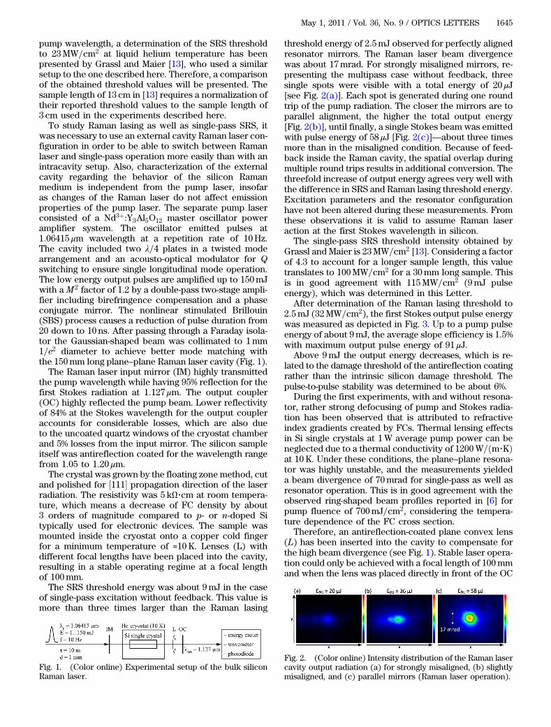
threshold energy of 2:5mJ observed for perfectly alignedresonator mirrors. The Raman laser beam divergencewas about 17mrad. For strongly misaligned mirrors, re-presenting the multipass case without feedback, threesingle spots were visible with a total energy of 20 μJ[see Fig. 2(a)]. Each spot is generated during one roundtrip of the pump radiation. The closer the mirrors are toparallel alignment, the higher the total output energy[Fig. 2(b)], until finally, a single Stokes beam was emittedwith pulse energy of 58 μJ [Fig. 2(c)]—about three timesmore than in the misaligned condition. Because of feed-back inside the Raman cavity, the spatial overlap duringmultiple round trips results in additional conversion. Thethreefold increase of output energy agrees very well withthe difference in SRS and Raman lasing threshold energy.Excitation parameters and the resonator configurationhave not been altered during these measurements. Fromthese observations it is valid to assume Raman laseraction at the first Stokes wavelength in silicon.
The single-pass SRS threshold intensity obtained byGrassl and Maier is 23MW=cm2 [13]. Considering a factorof 4.3 to account for a longer sample length, this valuetranslates to 100MW=cm2 for a 30mm long sample. Thisis in good agreement with 115MW=cm2 (9mJ pulseenergy), which was determined in this Letter.
After determination of the Raman lasing threshold to2:5mJ (32MW=cm2), the first Stokes output pulse energywas measured as depicted in Fig. 3. Up to a pump pulseenergy of about 9mJ, the average slope efficiency is 1.5%with maximum output pulse energy of 91 μJ.
Above 9mJ the output energy decreases, which is re-lated to the damage threshold of the antireflection coatingrather than the intrinsic silicon damage threshold. Thepulse-to-pulse stability was determined to be about 6%.
During the first experiments, with and without resona-tor, rather strong defocusing of pump and Stokes radia-tion has been observed that is attributed to refractiveindex gradients created by FCs. Thermal lensing effectsin Si single crystals at 1W average pump power can beneglected due to a thermal conductivity of 1200W=ðm⋅KÞat 10K. Under these conditions, the plane–plane resona-tor was highly unstable, and the measurements yieldeda beam divergence of 70mrad for single-pass as well asresonator operation. This is in good agreement with theobserved ring-shaped beam profiles reported in [6] forpump fluence of 700mJ=cm2, considering the tempera-ture dependence of the FC cross section.
Therefore, an antireflection-coated plane convex lens(L) has been inserted into the cavity to compensate forthe high beam divergence (see Fig. 1). Stable laser opera-tion could only be achieved with a focal length of 100mmand when the lens was placed directly in front of the OC
Fig. 1. (Color online) Experimental setup of the bulk siliconRaman laser.
Fig. 2. (Color online) Intensity distribution of the Raman lasercavity output radiation (a) for strongly misaligned, (b) slightlymisaligned, and (c) parallel mirrors (Raman laser operation).
May 1, 2011 / Vol. 36, No. 9 / OPTICS LETTERS 1645

mirror. Replacement of this mirror–lens pair by a con-cave output coupler should provide better FC lens com-pensation and thus lower output beam divergence.For room-temperature operation of a Raman laser
with bulk Si and nanosecond pulse duration, the impactsof the FC cross section and FC losses need to be inves-tigated. The FC lifetime, however, is long at 10K or 300Kcompared to the pulse duration. To overcome the linearabsorption losses, the pump wavelength must be largerthan used here.The influence of FC absorption becomes insignificant
at even longer excitation wavelengths beyond 2:2 μmbecause of the drastically reduced probability for two-photon absorption being the dominant process for theFC generation [14]. A drawback lies in the reciprocalwavelength dependence of the gain coefficient [7].The temporal development of the Raman laser emis-
sion exhibits a delay to the pump pulse because of theintensity-dependent SRS threshold. If the pump pulse in-tensity reaches threshold intensity, the Raman conver-sion process is stimulated. In Fig. 4, the onset of theStokes pulse coincides with the peak region of the pumppulse, with energy far above threshold. When the pumppulse decays, the Stokes intensity is declining even
faster, as a reaction on decreasing pump power insidethe Raman laser cavity.
Therefore, the Stokes pulse duration of 2:5 ns is fourtimes shorter than the pump pulse duration. The SBS celltransforms the originally Gaussian pump pulse shapefrom the oscillator into a slightly asymmetric shape,which is imprinted on the generated Stokes pulse.
For detection of pump and first Stokes pulse energy, aGentec ED-200 and a Polytec RjP 735 energy meter wereused, respectively. The latter provided higher sensitivity,required to measure the low-energy Stokes signals. Tem-poral measurements have been carried out with fastphoto diodes (Thorlabs DET 210) and a 1GHz oscillo-scope (Tektronix TDS 680B). The Si sensor sensitivityis still sufficiently high at 1:127 μm to receive good signalintensity. The beam profile was recorded with a SpiriconSCOR20 Si-CCD camera. The output beam was directedinto a wavelength meter (HighFinesse Ångstrom WS-6IR)using Fizeau interferometers to determine the outputwavelength to 1:127 μm corresponding to the Raman shiftin silicon of 521 cm−1 (15:6THz).
The SRS wavelength is tunable by changing the pumplaser wavelength in combination with the Raman shift of521 cm−1. The transparency range between 1 and 10 μmallows operation of Si Raman shifters in the near- andmid-IR regions, which is much broader than for typicalinfrared transmission edges around 2 μm or 3 μm foroxide Raman crystals [15]. In future investigations strongimprovement of the resonator Q factor and use of longersample sizes can be implemented, so that output pulseenergy of several millijoules is expected.
This work was supported by the German Federal Min-istry of Education and Research (BMBF) within theresearch grant (13N9732) “SiliconLight.” Furthermore,the authors would like to thank H. Riemann and U. Judafrom the Leibniz-Institut für Kristallzüchtung (IKZ) inBerlin for growing, cutting, and polishing the Si crystals.
References
1. B. Jalali, V. Raghunathan, D. Dimitropoulos, and O. Boyraz,IEEE J. Sel. Top. Quantum Electron. 12, 412 (2006).
2. O. Boyraz and B. Jalali, Opt. Express 12, 5269 (2004).3. H. S. Rong, R. Jones, A. S. Liu, O. Cohen, D. Hak, A. Fang,
and M. Paniccia, Nature 433, 725 (2005).4. H. S. Rong, A. S. Liu, R. Jones, O. Cohen, D. Hak, R.
Nicolaescu, A. Fang, and M. Paniccia, Nature 433, 292(2005).
5. A. Z. Grasiuk, Quantum Electron. 4, 269 (1974).6. J. Chen and H. J. Eichler, Appl. Phys. B 45, 121 (1988).7. A. Penzkofer, A. Laubereau, and W. Kaiser, Prog. Quantum
Electron. 6, 56 (1979).8. J. T. Murray, W. L. Austin, and R. C. Powell, Opt. Mater. 11,
353 (1999).9. J. M. Ralston and R. K. Chang, Phys. Rev. B 2, 1858 (1970).10. R. Claps, D. Dimitropoulos, and B. Jalali, Electron. Lett. 38,
1352 (2002).11. W. Bludau, A. Onton, and W. Heinke, J. Appl. Phys. 45,
1846 (1974).12. K. G. Svantesson and N. G. Nilsson, J. Phys. C 12,
3837 (1979).13. H. P. Grassl and M. Maier, Opt. Commun. 30, 253 (1979).14. V. Raghunathan, R. Shori, O. M. Stafsudd, and B. Jalali,
Phys. Status Solidi A 203, R38 (2006).15. A. A. Kaminskii, L. Bohatý, P. Becker, H. J. Eichler, and
H. Rhee, Laser Phys. Lett. 7, 142 (2010).
Fig. 3. (Color online) First Stokes output pulse energy versuspump pulse energy for the Raman laser with silicon singlecrystal.
Fig. 4. (Color online) Temporal behavior of the pump (dashedcurve) and Stokes radiation (solid curve) of the Si Raman laserfar above threshold.
1646 OPTICS LETTERS / Vol. 36, No. 9 / May 1, 2011