Embed Size (px)
Citation preview
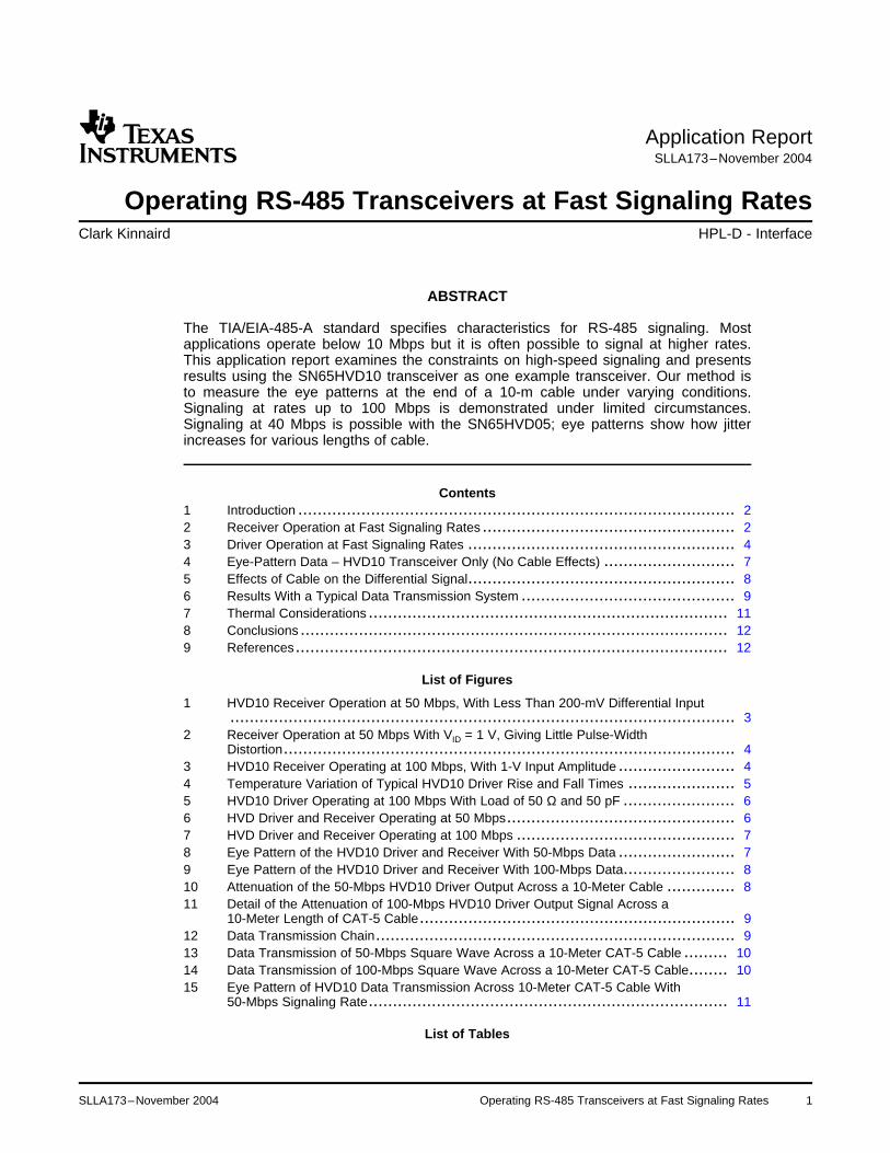
Application ReportSLLA173–November 2004
Operating RS-485 Transceivers at Fast Signaling RatesClark Kinnaird .......................................................................................................... HPL-D - Interface
ABSTRACT
The TIA/EIA-485-A standard specifies characteristics for RS-485 signaling. Mostapplications operate below 10 Mbps but it is often possible to signal at higher rates.This application report examines the constraints on high-speed signaling and presentsresults using the SN65HVD10 transceiver as one example transceiver. Our method isto measure the eye patterns at the end of a 10-m cable under varying conditions.Signaling at rates up to 100 Mbps is demonstrated under limited circumstances.Signaling at 40 Mbps is possible with the SN65HVD05; eye patterns show how jitterincreases for various lengths of cable.
Contents1 Introduction .......................................................................................... 22 Receiver Operation at Fast Signaling Rates .................................................... 23 Driver Operation at Fast Signaling Rates ....................................................... 44 Eye-Pattern Data – HVD10 Transceiver Only (No Cable Effects) ........................... 75 Effects of Cable on the Differential Signal....................................................... 86 Results With a Typical Data Transmission System ............................................ 97 Thermal Considerations .......................................................................... 118 Conclusions ........................................................................................ 129 References......................................................................................... 12
List of Figures
1 HVD10 Receiver Operation at 50 Mbps, With Less Than 200-mV Differential Input........................................................................................................ 3
2 Receiver Operation at 50 Mbps With VID = 1 V, Giving Little Pulse-WidthDistortion............................................................................................. 4
3 HVD10 Receiver Operating at 100 Mbps, With 1-V Input Amplitude ........................ 44 Temperature Variation of Typical HVD10 Driver Rise and Fall Times ...................... 55 HVD10 Driver Operating at 100 Mbps With Load of 50 Ω and 50 pF ....................... 66 HVD Driver and Receiver Operating at 50 Mbps............................................... 67 HVD Driver and Receiver Operating at 100 Mbps ............................................. 78 Eye Pattern of the HVD10 Driver and Receiver With 50-Mbps Data ........................ 79 Eye Pattern of the HVD10 Driver and Receiver With 100-Mbps Data....................... 810 Attenuation of the 50-Mbps HVD10 Driver Output Across a 10-Meter Cable .............. 811 Detail of the Attenuation of 100-Mbps HVD10 Driver Output Signal Across a
10-Meter Length of CAT-5 Cable................................................................. 912 Data Transmission Chain.......................................................................... 913 Data Transmission of 50-Mbps Square Wave Across a 10-Meter CAT-5 Cable ......... 1014 Data Transmission of 100-Mbps Square Wave Across a 10-Meter CAT-5 Cable........ 1015 Eye Pattern of HVD10 Data Transmission Across 10-Meter CAT-5 Cable With
50-Mbps Signaling Rate.......................................................................... 11
List of Tables
Operating RS-485 Transceivers at Fast Signaling RatesSLLA173–November 2004 1

www.ti.com
1 Introduction
2 Receiver Operation at Fast Signaling Rates
Introduction
1 Summary of Jitter vs Signaling Rate and Cable Length....................................... 92 Power Dissipation Comparisons ................................................................ 12
The data sheets for some of Texas Instruments RS-485 transceivers specify signaling rates up to 30Mbps. This is over all recommended operating conditions and with full compliance to the provisions of theANSI/TIA/EIA-485-A standard.
Many applications do not require specification to all worst-case conditions of temperature, cable distance,power supply variation, etc. For these applications, it is often possible to signal at faster rates. Thisapplication report examines the constraints on high-speed signaling and demonstrates operation atspeeds of 50 Mbps and faster.
The SN65HVD10 transceiver (hereafter referred to as the HVD10) is used as an example, but the basicdiscussions are valid for any of Texas Instruments RS-485 transceivers and line driver/line receivercircuits. (1).
The principal requirements for an RS-485 transceiver to operate at fast signaling rates are that thereceiver must accurately detect valid signal levels on the bus, and the driver must successfully generatevalid bus states. Another concern at fast signaling rates is that the transceiver dissipates more power thanat slower rates.
(1) Several of Texas Instruments RS-485 devices include a feature which intentionally limits the driver slew rate. Although the basicdiscussions are still valid for these devices, drivers with slew-rate limiting are optimized for slower signaling rates.
The ANSI/TIA/EIA-485-A standard requires a receiver to detect any differential bus voltage (VA- VB) withamplitude of greater than 200 mV as a valid data state. Therefore, the worst-case input for a receiver hasamplitude of only 200 mV.
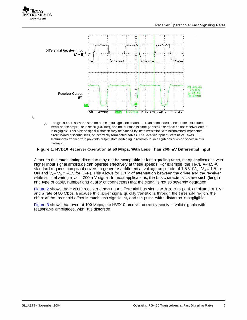
Figure 1 shows the HVD10 receiver detecting a differential bus signal consisting of a square wave withzero-to-peak amplitude of slightly less than 200 mV at nominal conditions (2). The signal frequency is 25MHz, corresponding to a signaling rate of 50 Mbps. Although the HVD10 receiver output is changing statecorrectly in response to the bus signal, there is significant pulse-width distortion due to the offset in theHVD10 receiver thresholds. That is, the passive fail-safe feature requires that a 0-mV differential signal bedetected as a known state. Therefore, the receiver thresholds (VIT+ and VIT-) for the HVD10 are centeredon –105 mV. Because the input signal is centered on zero and has finite edge transition times, more of theinput signal is above the receiver threshold than is below it. This causes significant pulse-width distortionfor the specific case of high data rates with low signal amplitudes.
(2) All the following oscilloscope plots were taken at room temperature with VCC set to 3.3 V.
Operating RS-485 Transceivers at Fast Signaling Rates2 SLLA173–November 2004
www.ti.com
Differential Receiver Input(A − B)
Receiver Output(R)
Receiver Operation at Fast Signaling Rates
A.
(1) The glitch or crossover distortion of the input signal on channel 1 is an unintended effect of the test fixture.Because the amplitude is small (±40 mV), and the duration is short (2 nsec), the effect on the receiver outputis negligible. This type of signal distortion may be caused by instrumentation with mismatched impedance,circuit-board discontinuities, or incorrectly terminated cables. The receiver input hysteresis of TexasInstruments transceivers prevents output state switching in reaction to small glitches such as shown in thisexample.
Figure 1. HVD10 Receiver Operation at 50 Mbps, With Less Than 200-mV Differential Input
Although this much timing distortion may not be acceptable at fast signaling rates, many applications withhigher input signal amplitude can operate effectively at these speeds. For example, the TIA/EIA-485-Astandard requires compliant drivers to generate a differential voltage amplitude of 1.5 V (VA– VB = 1.5 forON and VA– VB = –1.5 for OFF). This allows for 1.3 V of attenuation between the driver and the receiverwhile still delivering a valid 200 mV signal. In most applications, the bus characteristics are such (lengthand type of cable, number and quality of connectors) that the signal is not so severely degraded.
Figure 2 shows the HVD10 receiver detecting a differential bus signal with zero-to-peak amplitude of 1 Vand a rate of 50 Mbps. Because this larger signal quickly transitions through the threshold region, theeffect of the threshold offset is much less significant, and the pulse-width distortion is negligible.
Figure 3 shows that even at 100 Mbps, the HVD10 receiver correctly receives valid signals withreasonable amplitudes, with little distortion.
Operating RS-485 Transceivers at Fast Signaling RatesSLLA173–November 2004 3

www.ti.com
Differential Receiver Input(A − B)
Receiver Output(R)
Receiver Input(A − B)
Receiver Output(R)
3 Driver Operation at Fast Signaling Rates
Driver Operation at Fast Signaling Rates
Figure 2. Receiver Operation at 50 Mbps With VID = 1 V, Giving Little Pulse-Width Distortion
Figure 3. HVD10 Receiver Operating at 100 Mbps, With 1-V Input Amplitude
In order to comply with the TIA/EIA-485-A standard, a driver must meet several criteria. One of these is togenerate balanced differential voltage levels. Another requirement restricts the 10%-to-90% transition timeto 30% of the unit interval (bit time). Therefore, there is an inverse relationship between the driver outputrise and fall times and the maximum achievable signaling rate.
Under all recommended operating conditions, the HVD10 driver is specified to have rise and fall times notexceeding 10 nanoseconds. This corresponds to a maximum achievable signaling rate (for ALLrecommended operating conditions) of 30 Mbps. However, reasonable assumptions can be made whichextend the possible signaling rate for many applications
One reasonable assumption is that in some applications the driver may not be subjected to the entiretemperature range for which the HVD10 is specified. The HVD10 is available in different temperaturegrades:
Operating RS-485 Transceivers at Fast Signaling Rates4 SLLA173–November 2004
www.ti.com
5
6
7
8
9
10
−55 −35 −15 5 25 45 65 85 105 125
HV
D10
Dri
ver
Ris
e/F
all T
ime
VCC = 3 V
VCC = 3.6 V
VCC = 3.3 V
TA − Free-Air Temperature − C
Driver Operation at Fast Signaling Rates
Different Temperature Grades
SN75 0ºC to 70ºC
SN65 –40ºC to 85ºC
SN65_Q –40ºC to 125ºC
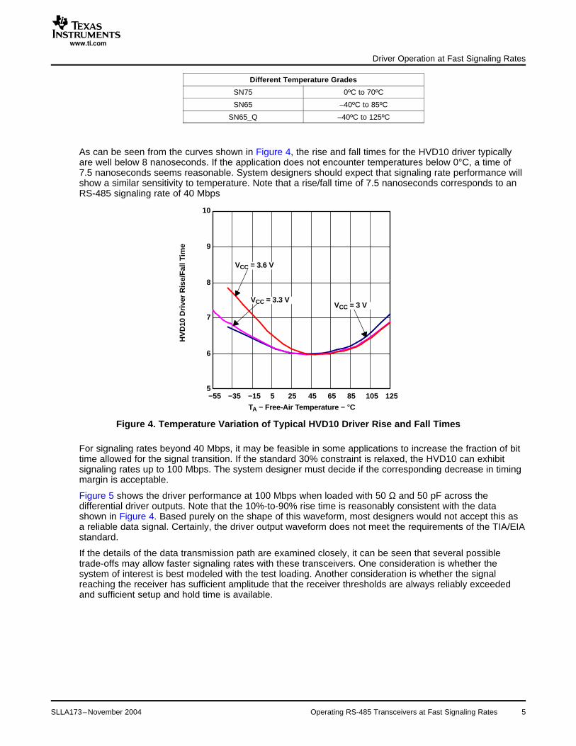
As can be seen from the curves shown in Figure 4, the rise and fall times for the HVD10 driver typicallyare well below 8 nanoseconds. If the application does not encounter temperatures below 0°C, a time of7.5 nanoseconds seems reasonable. System designers should expect that signaling rate performance willshow a similar sensitivity to temperature. Note that a rise/fall time of 7.5 nanoseconds corresponds to anRS-485 signaling rate of 40 Mbps
Figure 4. Temperature Variation of Typical HVD10 Driver Rise and Fall Times
For signaling rates beyond 40 Mbps, it may be feasible in some applications to increase the fraction of bittime allowed for the signal transition. If the standard 30% constraint is relaxed, the HVD10 can exhibitsignaling rates up to 100 Mbps. The system designer must decide if the corresponding decrease in timingmargin is acceptable.
Figure 5 shows the driver performance at 100 Mbps when loaded with 50 Ω and 50 pF across thedifferential driver outputs. Note that the 10%-to-90% rise time is reasonably consistent with the datashown in Figure 4. Based purely on the shape of this waveform, most designers would not accept this asa reliable data signal. Certainly, the driver output waveform does not meet the requirements of the TIA/EIAstandard.
If the details of the data transmission path are examined closely, it can be seen that several possibletrade-offs may allow faster signaling rates with these transceivers. One consideration is whether thesystem of interest is best modeled with the test loading. Another consideration is whether the signalreaching the receiver has sufficient amplitude that the receiver thresholds are always reliably exceededand sufficient setup and hold time is available.
Operating RS-485 Transceivers at Fast Signaling RatesSLLA173–November 2004 5

www.ti.com
Driver Input(D)
Differential Driver Output(A − B)
Differential Driver Output(A − B)
Receiver Output(R)
Driver Operation at Fast Signaling Rates
Figure 5. HVD10 Driver Operating at 100 Mbps With Load of 50 Ω and 50 pF
To illustrate the first consideration, Figure 6 and Figure 7 show the outputs of a driver and a receiver, withnegligible cable length connecting them. Note that in these cases there is only the 51 Ω load and thecapacitance of the test board, cable, and connectors across the outputs. Comparing Figure 7 to Figure 5,it is obvious that the load capacitance plays a significant role in signal transition time and quality, affectingthe maximum possible signaling rate. Therefore, it is important to model the system of interest in terms ofload capacitance. Subsequent sections discuss the results with actual cable, rather than with a lumpedcapacitive load. In Figure 6 and Figure 7, channel 1 is the differential driver output with a 51-Ω load, andchannel 2 is the receiver output.
Figure 6. HVD Driver and Receiver Operating at 50 Mbps
Operating RS-485 Transceivers at Fast Signaling Rates6 SLLA173–November 2004

www.ti.com
Differential Driver Output(A − B)
Receiver Output(R)
4 Eye-Pattern Data – HVD10 Transceiver Only (No Cable Effects)
Differential Driver Output(A − B)
Receiver Output(R)
Eye-Pattern Data – HVD10 Transceiver Only (No Cable Effects)
Figure 7. HVD Driver and Receiver Operating at 100 Mbps
One measure of system performance at high signaling rates is data signal jitter . Eye patterns (1) can beused to visualize the jitter at various points in the system. Jitter at the driver output is one component oftotal system jitter. Figure 8 and Figure 9 illustrate that the HVD10 contributes a small amount of jitter at 50Mbps, and a larger contribution at signaling rates of 100 Mbps. Channel 1 is the driver output; channel 2 isthe receiver output.
Figure 8. Eye Pattern of the HVD10 Driver and Receiver With 50-Mbps Data(1) For a discussion of eye-pattern measurements, see Section 4 of Texas Instruments application report, Interface Circuits for TIA/EIA-485
(RS-485) (SLLA036)
Operating RS-485 Transceivers at Fast Signaling RatesSLLA173–November 2004 7
www.ti.com
Differential Driver Output(A − B)
Receiver Output(R)
5 Effects of Cable on the Differential Signal
Driver Output(Before Cable)
Receiver Input(After Cable)
Effects of Cable on the Differential Signal
Figure 9. Eye Pattern of the HVD10 Driver and Receiver With 100-Mbps Data
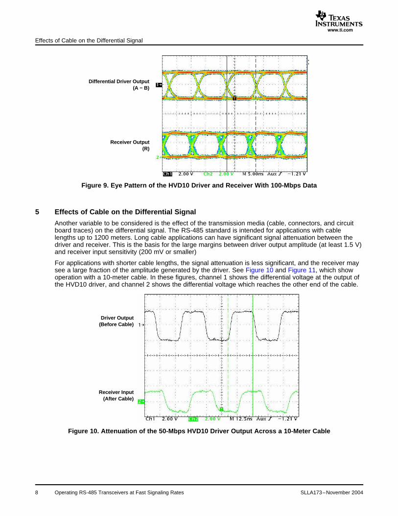
Another variable to be considered is the effect of the transmission media (cable, connectors, and circuitboard traces) on the differential signal. The RS-485 standard is intended for applications with cablelengths up to 1200 meters. Long cable applications can have significant signal attenuation between thedriver and receiver. This is the basis for the large margins between driver output amplitude (at least 1.5 V)and receiver input sensitivity (200 mV or smaller)
For applications with shorter cable lengths, the signal attenuation is less significant, and the receiver maysee a large fraction of the amplitude generated by the driver. See Figure 10 and Figure 11, which showoperation with a 10-meter cable. In these figures, channel 1 shows the differential voltage at the output ofthe HVD10 driver, and channel 2 shows the differential voltage which reaches the other end of the cable.
Figure 10. Attenuation of the 50-Mbps HVD10 Driver Output Across a 10-Meter Cable
Operating RS-485 Transceivers at Fast Signaling Rates8 SLLA173–November 2004
www.ti.com
Driver Output(Before Cable)
Receiver Input(After Cable)
6 Results With a Typical Data Transmission System
+
−
+
−
VOD VIDVI VO
Results With a Typical Data Transmission System
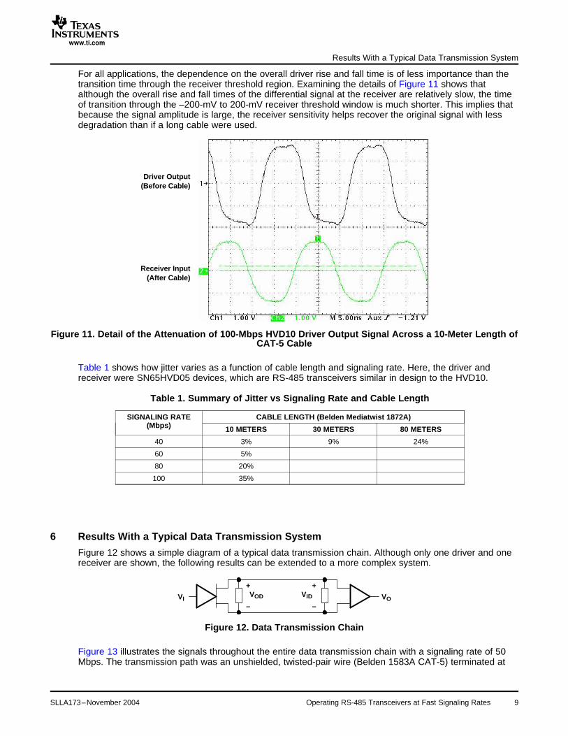
For all applications, the dependence on the overall driver rise and fall time is of less importance than thetransition time through the receiver threshold region. Examining the details of Figure 11 shows thatalthough the overall rise and fall times of the differential signal at the receiver are relatively slow, the timeof transition through the –200-mV to 200-mV receiver threshold window is much shorter. This implies thatbecause the signal amplitude is large, the receiver sensitivity helps recover the original signal with lessdegradation than if a long cable were used.
Figure 11. Detail of the Attenuation of 100-Mbps HVD10 Driver Output Signal Across a 10-Meter Length ofCAT-5 Cable
Table 1 shows how jitter varies as a function of cable length and signaling rate. Here, the driver andreceiver were SN65HVD05 devices, which are RS-485 transceivers similar in design to the HVD10.
Table 1. Summary of Jitter vs Signaling Rate and Cable Length
SIGNALING RATE CABLE LENGTH (Belden Mediatwist 1872A)(Mbps) 10 METERS 30 METERS 80 METERS
40 3% 9% 24%
60 5%
80 20%
100 35%
Figure 12 shows a simple diagram of a typical data transmission chain. Although only one driver and onereceiver are shown, the following results can be extended to a more complex system.
Figure 12. Data Transmission Chain
Figure 13 illustrates the signals throughout the entire data transmission chain with a signaling rate of 50Mbps. The transmission path was an unshielded, twisted-pair wire (Belden 1583A CAT-5) terminated at
Operating RS-485 Transceivers at Fast Signaling RatesSLLA173–November 2004 9

www.ti.com
VI
VOD
VID
VO
VI
VOD
VID
VO
Results With a Typical Data Transmission System
each end with an approximate 100-Ω resistor. Channel 1 is the TTL input to the driver, and channel 2shows the differential driver output. Channel 3 shows the differential signal that reaches the input to theHVD10 receiver after the 10-meter length of cable. Note that the signal that reaches the receiver has beenattenuated, especially the high-frequency components, reducing both the amplitude and the edge rates.Channel 4 shows the output of the receiver.
Figure 13. Data Transmission of 50-Mbps Square Wave Across a 10-Meter CAT-5 Cable
Although the transmission channel has degraded the signal, the final digital signal matches the originalinput. This illustrates that the HVD10 can achieve signaling rates of 50 Mbps. Signaling rates as high as100 Mbps are possible, as shown in Figure 14.
Figure 14 shows the operation at 100 Mbps through the same signal chain as previously described. Here,the input signal to the receiver appears more as a sinusoid than a square wave, due to the combinedeffects of the driver’s finite rise and fall times, and the high-frequency attenuation of the cable
Figure 14. Data Transmission of 100-Mbps Square Wave Across a 10-Meter CAT-5 Cable
In spite of the appearance of the receiver’s input, the receiver output is a reasonable square wave,reflecting the original signal at the source of the driver. This indicates that 100-Mbps data transmission ispossible using the HVD10 transceiver.
Operating RS-485 Transceivers at Fast Signaling Rates10 SLLA173–November 2004

www.ti.com
VI
VOD
VID
VO
7 Thermal Considerations
Thermal Considerations
Practically, the square-wave signals (clock signals) shown in Figure 13 and Figure 14 are notrepresentative of most RS-485 applications. A more general signal is represented by a pseudo-random bitstream (PRBS) of binary data. Such a PRBS signal typically includes all significant combinations of bitsand is used to generate an eye pattern as a measure of data transmission system quality.
The oscilloscope traces in Figure 15 illustrate successful 50-Mbps data transmission using two HVD10transceivers and a cable length of 10 meters. The signal was a PRBS. Channel 1 shows the TTL input tothe driver; channel 2 shows the differential driver output. Channel 3 shows the differential signal thatreaches the input to the HVD10 receiver and channel 4 shows the TTL output of the receiver.
Figure 15. Eye Pattern of HVD10 Data Transmission Across 10-Meter CAT-5 Cable With 50-MbpsSignaling Rate
Power dissipation and thermal issues must always be considered, especially in industrial applicationswhere RS-485 transceivers are commonly used. Designers for fast-signaling rate applications should payclose attention to the increased power dissipation inherent in those cases.
In a data bus network, power supply current is delivered to the bus load as well as to the transceivercircuitry. For a typical RS-485 bus configuration, the steady-state load that an active driver must driveconsists of all the receiving nodes, plus the termination resistors at each end of the bus.
The load presented by the receiving nodes depends on the input impedance of each receiver. TheTIA/EIA-485-A standard defines a unit load (1) allowing up to 1 mA. With up to 32 unit loads allowed on thebus, the total current supplied to all receivers can be as high as 32 mA. Many transceivers now aredesigned with reduced unit loading; for example, the HVD10 is a 1/2-unit-load device, and theSN65HVD3088E is rated as a 1/8 unit-load device. These reduced unit-loading devices have correspond-ingly lower input current.
The current in the termination resistors depends on the differential bus voltage. The standard requiresactive drivers to produce at least 1.5 V of differential signal. For a bus terminated with one standard 120-Ωresistor at each end, this sums to 25 mA in the termination resistors whenever the bus is active. TexasInstruments transceivers typically can drive more than 25 mA to a 60-Ω load, resulting in a differentialoutput voltage higher than the minimum required by the standard.
Overall, the total steady-state load current can typically be 60 mA to a fully loaded RS-485 bus. This is inaddition to the current required by the transceiver.
(1) For more details on the unit load, see TI application report The RS-485 Unit Load and Maximum Number of Bus Connections,(SLLA166).
Operating RS-485 Transceivers at Fast Signaling RatesSLLA173–November 2004 11

www.ti.com
8 Conclusions
9 References
Conclusions
Supply current increases with signaling rate primarily due to the totem-pole outputs of the driver. Whenthese outputs change state, for a moment, both the high-side and low-side output transistors areconducting. This creates a short spike in the supply current. As the frequency of state changes increases,more power is used as these short spikes of current occur more frequently, leading to a marked increasein the overall power dissipation.
A secondary increase in power consumption occurs due to capacitive effects. The capacitive elements arefound both internal to the transceiver and in the external load. The external load capacitance is oftenmodeled as a lumped 50 pF, as shown in the data sheet test circuit schematics. This 50 pF representstest fixture and instrumentation capacitance because the inductance of the short interconnect is negligible.The internal capacitance is due to the transceiver circuitry and is typically approximately 5 pF to 10 pF.
Table 2 illustrates how power dissipation is affected by signaling rate, as well as by the mode of operation.In each case, the maximum power dissipation takes into account variations in power supply, temperature,etc., while the typical values reflect the power dissipation under nominal conditions.
Table 2. Power Dissipation Comparisons
SIGNALING DRIVER LOAD RECEIVER LOAD MODE TRANSCEIVER POWERRATE DISSIPATION
100 Mbps 60 Ω, 50 pF 15 pF Driver enabled and Receiver 387 mW (maximum)enabled
50 Mbps Driver enabled and Receiver 296 mW (maximum)enabled
32 Mbps Driver enabled and Receiver 256 mW (maximum)enabled
Driver enabled and Receiver 245 mW (maximum)disabled
Driver disabled and Receiver 32 mW (maximum)enabled 20 mW (typical)
25 Mbps Driver enabled and Receiver 233 mW (maximum)enabled 198 mW (typical)
Designers should take the higher power dissipation at fast signaling rates into account. For additionalinformation on thermal design, see the individual device data sheets and Texas Instruments applicationnotes IC Package Thermal Metrics (SPRA953) and Thermal Characteristics of Linear and Logic PackagesUsing JEDEC PCB Designs (SZZA017).
Texas Instruments data sheets are intentionally conservative in regard to the highest possible signalingrate and the signal-quality requirements of TIA/EIA-485-A. The HVD10 transceiver can successfullyoperate at fast signaling rates, up to 50 Mbps or even 100 Mbps. The system designer must considerlimiting constraints, such as compliance to RS-485 standards, application temperature, and cable effectswhen determining how far to push the envelope in terms of signaling rate.
Similarly, system designers must consider the parametric limitations of other RS-485 devices in extendingthe performance beyond worst-case minimums. Depending on the application, signaling rates significantlyhigher than the minimum claims may be possible. The ultimate top signaling rate can only be determinedat the final installation.
1. Interface Circuits for TIA/EIA-485 (RS-485) application report (SLLA036)2. The RS-485 Unit Load and Maximum Number of Bus Connections application report (SLLA166)
Operating RS-485 Transceivers at Fast Signaling Rates12 SLLA173–November 2004

IMPORTANT NOTICE
Texas Instruments Incorporated and its subsidiaries (TI) reserve the right to make corrections, modifications,enhancements, improvements, and other changes to its products and services at any time and to discontinueany product or service without notice. Customers should obtain the latest relevant information before placingorders and should verify that such information is current and complete. All products are sold subject to TI’s termsand conditions of sale supplied at the time of order acknowledgment.
TI warrants performance of its hardware products to the specifications applicable at the time of sale inaccordance with TI’s standard warranty. Testing and other quality control techniques are used to the extent TIdeems necessary to support this warranty. Except where mandated by government requirements, testing of allparameters of each product is not necessarily performed.
TI assumes no liability for applications assistance or customer product design. Customers are responsible fortheir products and applications using TI components. To minimize the risks associated with customer productsand applications, customers should provide adequate design and operating safeguards.
TI does not warrant or represent that any license, either express or implied, is granted under any TI patent right,copyright, mask work right, or other TI intellectual property right relating to any combination, machine, or processin which TI products or services are used. Information published by TI regarding third-party products or servicesdoes not constitute a license from TI to use such products or services or a warranty or endorsement thereof.Use of such information may require a license from a third party under the patents or other intellectual propertyof the third party, or a license from TI under the patents or other intellectual property of TI.
Reproduction of information in TI data books or data sheets is permissible only if reproduction is withoutalteration and is accompanied by all associated warranties, conditions, limitations, and notices. Reproductionof this information with alteration is an unfair and deceptive business practice. TI is not responsible or liable forsuch altered documentation.
Resale of TI products or services with statements different from or beyond the parameters stated by TI for thatproduct or service voids all express and any implied warranties for the associated TI product or service andis an unfair and deceptive business practice. TI is not responsible or liable for any such statements.
Following are URLs where you can obtain information on other Texas Instruments products and applicationsolutions:
Products Applications
Amplifiers amplifier.ti.com Audio www.ti.com/audio
Data Converters dataconverter.ti.com Automotive www.ti.com/automotive
DSP dsp.ti.com Broadband www.ti.com/broadband
Interface interface.ti.com Digital Control www.ti.com/digitalcontrol
Logic logic.ti.com Military www.ti.com/military
Power Mgmt power.ti.com Optical Networking www.ti.com/opticalnetwork
Microcontrollers microcontroller.ti.com Security www.ti.com/security
Telephony www.ti.com/telephony
Video & Imaging www.ti.com/video
Wireless www.ti.com/wireless
Mailing Address: Texas Instruments
Post Office Box 655303 Dallas, Texas 75265
Copyright 2004, Texas Instruments Incorporated