Embed Size (px)
Citation preview
Open foundry platform for high-performance
electronic-photonic integration
Jason S. Orcutt,1,*
Benjamin Moss,1 Chen Sun,
1 Jonathan Leu,
1 Michael Georgas,
1
Jeffrey Shainline,2 Eugen Zgraggen,
1 Hanqing Li,
1 Jie Sun,
1 Matthew Weaver,
1
Stevan Urošević,1,2
Miloš Popović,2 Rajeev J. Ram
1 and Vladimir Stojanović
1
1Department of Electrical Engineering and Computer Science, Massachusetts Institute of Technology, 77
Massachusetts Ave, Cambridge, Massachusetts 02139, USA 2Department of Electrical, Computer and Energy Engineering, University of Colorado at Boulder, Boulder,
Colorado 80309, USA *[email protected]
Abstract: This paper presents photonic devices with 3 dB/cm waveguide
loss fabricated in an existing commercial electronic 45 nm SOI-CMOS
foundry process. By utilizing existing front-end fabrication processes the
photonic devices are monolithically integrated with electronics in the same
physical device layer as transistors achieving 4 ps logic stage delay, without
degradation in transistor performance. We demonstrate an 8-channel optical
microring-resonator filter bank and optical modulators, both controlled by
integrated digital circuits. By developing a device design methodology that
requires zero process infrastructure changes, a widely available platform for
high-performance photonic-electronic integrated circuits is enabled.
©2012 Optical Society of America
OCIS codes: (250.3140) Integrated optoelectronic circuits; (250.7360) Waveguide modulators;
(250.5300) Photonic integrated circuits.
References and links
1. M. Hochberg and T. Baehr-Jones, “Towards fabless silicon photonics,” Nat. Photonics 4(8), 492–494 (2010).
2. P. Dumon, W. Bogaerts, R. Baets, J. M. Fedeli, and L. Fulbert, “Towards foundry approach for silicon
photonics: silicon photonics platform ePIXfab,” Electron. Lett. 45, 13–14 (2009).
3. M. Hochberg, “Fabless nanophotonics,” in Conference on Lasers and Electro-Optics (Optical Society of
America, 2011), CWM1.
4. C. Gunn, “CMOS photonics for high-speed interconnects,” IEEE Micro 26(2), 58–66 (2006).
5. L. C. Kimerling, D. Ahn, A. B. Apsel, M. Beals, D. Carothers, Y. K. Chen, T. Conway, D. M. Gill, M. Grove, C.
Y. Hong, M. Lipson, J. Liu, J. Michel, D. Pan, S. S. Patel, A. T. Pomerene, M. Rasras, D. K. Sparacin, K. Y. Tu,
A. E. White, and C. W. Wong, “Electronic-photonic integrated circuits on the CMOS platform,” Proc. SPIE
6125, 6–15 (2006).
6. Y. Vlasov, W. M. J. Green, and F. Xia, “High-throughput silicon nanophotonic wavelength-insensitive switch
for on-chip optical networks,” Nat. Photonics 2(4), 242–246 (2008).
7. I. A. Young, E. Mohammed, J. T. S. Liao, A. M. Kern, S. Palermo, B. A. Block, M. R. Reshotko, and P. L. D.
Chang, “Optical I/O technology for tera-scale computing,” IEEE J. Solid-St. Circulation 45, 235–248 (2010).
8. W. A. Zortman, D. C. Trotter, A. L. Lentine, G. Robertson, and M. R. Watts, “Monolithic integration of silicon
electronics and photonics,” in Winter Topicals (IEEE 2011), 139–140.
9. J. S. Orcutt, A. Khilo, C. W. Holzwarth, M. A. Popović, H. Li, J. Sun, T. Bonifield, R. Hollingsworth, F. X.
Kärtner, H. I. Smith, V. Stojanović, and R. J. Ram, “Nanophotonic integration in state-of-the-art CMOS
foundries,” Opt. Express 19(3), 2335–2346 (2011).
10. S. Narasimha, K. Onishi, H. M. Nayfeh, A. Waite, M. Weybright, J. Johnson, C. Fonseca, D. Corliss, C.
Robinson, M. Crouse, D. Yang, C. H. J. Wu, A. Gabor, T. Adam, I. Ahsan, M. Belyansky, L. Black, S. Butt, J.
Cheng, A. Chou, G. Costrini, C. Dimitrakopoulos, A. Domenicucci, P. Fisher, A. Frye, S. Gates, S. Greco, S.
Grunow, M. Hargrove, J. Holt, S. J. Jeng, M. Kelling, B. Kim, W. Landers, G. Larosa, D. Lea, M. H. Lee, X.
Liu, N. Lustig, A. McKnight, L. Nicholson, D. Nielsen, K. Nummy, V. Ontalus, C. Ouyang, X. Ouyang, C.
Prindle, R. Pal, W. Rausch, D. Restaino, C. Sheraw, J. Sim, A. Simon, T. Standaert, C. Y. Sung, K. Tabakman,
C. Tian, R. Van Den Nieuwenhuizen, H. Van Meer, A. Vayshenker, D. Wehella-Gamage, J. Werking, R. C.
Wong, J. Yu, S. Wu, R. Augur, D. Brown, X. Chen, D. Edelstein, A. Grill, M. Khare, Y. Li, S. Luning, J.
Norum, S. Sankaran, D. Schepis, R. Wachnik, R. Wise, C. Warm, T. Ivers, and P. Agnello, “High performance
45-nm SOI technology with enhanced strain, porous low-k BEOL, and immersion lithography,” in International
Electron Devices Meeting (IEEE, 2006), 1–4.
#163082 - $15.00 USD Received 15 Feb 2012; revised 29 Mar 2012; accepted 2 Apr 2012; published 15 May 2012(C) 2012 OSA 21 May 2012 / Vol. 20, No. 11 / OPTICS EXPRESS 12222
11. J. Youn, M. Lee, K. Park, and W. Choi, “A 10-Gb/s 850-nm CMOS OEIC Receiver with a Silicon Avalanche
Photodetector,” IEEE J. Quantum Electron. 48(2), 229–236 (2012).
12. B. Jang and A. Hassibi, “Biosensor systems in standard CMOS processes: fact or fiction?” IEEE Trans. Ind.
Electron. 56(4), 979–985 (2009).
13. Akustica, “Technology,” retrieved February 7, 2012, http://www.akustica.com/Technology.asp.
14. C.-L. Dai, F.-Y. Xiao, Y.-Z. Juang, and C.-F. Chiu, “An approach to fabricating microstructures that incorporate
circuits using a post-CMOS process,” J. Micromech. Microeng. 15(1), 98–103 (2005).
15. R. Kalla, B. Sinharoy, W. J. Starke, and M. Floyd, “Power7: IBM's next-generation server processor,” IEEE
Micro 30(2), 7–15 (2010).
16. L. Sungjae, B. Jagannathan, S. Narasimha, A. Chou, N. Zamdmer, J. Johnson, R. Williams, L. Wagner, K.
Jonghae, J. O. Plouchart, J. Pekarik, S. Springer, and G. Freeman, “Record RF performance of 45-nm SOI
CMOS Technology,” in Electron Devices Meeting (IEEE 2007), 255–258.
17. J. S. Orcutt and R. J. Ram, “Photonic device layout within the foundry CMOS design environment,” IEEE
Photon. Technol. Lett. 22(8), 544–546 (2010).
18. J. S. Orcutt, A. Khilo, M. A. Popovic, C. W. Holzwarth, B. Moss, L. Hanqing, M. S. Dahlem, T. D. Bonifield, F.
X. Kartner, E. P. Ippen, J. L. Hoyt, R. J. Ram, and V. Stojanovic, “Demonstration of an electronic photonic
integrated circuit in a commercial scaled bulk CMOS process,” in Conference on Lasers and Electro-Optics
(Optical Society of America, 2008), CTuBB3.
19. J. S. Orcutt, “Scaled CMOS photonics,” in Photonics in Switching (Optical Society of America, 2010), PMC4.
20. S. Sridaran and S. A. Bhave, “Nanophotonic devices on thin buried oxide Silicon-On-Insulator substrates,” Opt.
Express 18(4), 3850–3857 (2010).
21. P. Dong, W. Qian, H. Liang, R. Shafiiha, N.-N. Feng, D. Feng, X. Zheng, A. V. Krishnamoorthy, and M.
Asghari, “Low power and compact reconfigurable multiplexing devices based on silicon microring resonators,”
Opt. Express 18(10), 9852–9858 (2010).
22. F. N. Xia, L. Sekaric, and Y. Vlasov, “Ultracompact optical buffers on a silicon chip,” Nat. Photonics 1(1), 65–
71 (2007).
23. S. K. Selvaraja, P. Jaenen, W. Bogaerts, D. V. Thourhout, P. Dumon, and R. Baets, “Fabrication of photonic
wire and crystal circuits in silicon-on-insulator using 193-nm optical lithography,” J. Lightwave Tech. 27(18),
4076–4083 (2009).
24. M. A. Popovic, T. Barwicz, E. Ippen, and F. X. Kärtner, “Global design rules for silicon microphotonic
waveguides: sensitivity, polarization and resonance tunability,” in Conference on Lasers and Electro-Optics
(Optical Society of America, 2006), CTuCC1.
25. M. A. Popovic, Theory and design of high-index-contrast microphotonic circuits (Massachusetts Institute of
Technology, 2008).
26. D. A. B. Miller, “Device requirements for optical interconnects to silicon chips,” Proc. IEEE 97(7), 1166–1185
(2009).
27. M. Georgas, J. Leu, B. Moss, S. Chen, and V. Stojanovic, “Addressing link-level design tradeoffs for integrated
photonic interconnects,” in Custom Integrated Circuits Conference (IEEE, 2011), 1–8.
28. P. Dong, W. Qian, H. Liang, R. Shafiiha, X. Wang, D. Feng, G. Li, J. E. Cunningham, A. V. Krishnamoorthy,
and M. Asghari, “1x4 reconfigurable demultiplexing filter based on free-standing silicon racetrack resonators,”
Opt. Express 18(24), 24504–24509 (2010).
29. M. Georgas, J. Orcutt, R. J. Ram, and V. Stojanovic, “A monolithically-integrated optical receiver in standard
45-nm SOI,” in European Solid State Circuits Conference (IEEE, 2011), 407–410.
30. J. Leu and V. Stojanovic, “Injection-locked clock receiver for monolithic optical link in 45nm SOI,” in Asian
Solid State Circuits Conference (IEEE, 2011), 149–152.
31. Q. Xu, B. Schmidt, S. Pradhan, and M. Lipson, “Micrometre-scale silicon electro-optic modulator,” Nature
435(7040), 325–327 (2005).
32. Q. Xu, S. Manipatruni, B. Schmidt, J. Shakya, and M. Lipson, “12.5 Gbit/s carrier-injection-based silicon micro-
ring silicon modulators,” Opt. Express 15(2), 430–436 (2007).
33. F. Liu, D. Patil, J. Lexau, P. Amberg, M. Dayringer, J. Gainsley, H. F. Moghadam, Z. Xuezhe, J. E.
Cunningham, A. V. Krishnamoorthy, E. Alon, and R. Ho, “10 Gbps, 530 fJ/b optical transceiver circuits in 40
nm CMOS,” in Symposium on VLSI Circuits (IEEE, 2011), 290–291.
34. M. R. Watts, W. A. Zortman, D. C. Trotter, R. W. Young, and A. L. Lentine, “Vertical junction silicon
microdisk modulators and switches,” Opt. Express 19(22), 21989–22003 (2011).
1. Introduction
Standardized fabrication of microchips with silicon photonic devices and circuits in multi-
user fabrication facilities, known as foundries, promises to dramatically increase the pace of
technology innovation in ways analogous to the late 20th-century transformation of the
CMOS electronics industry [1]. Recently, photonics-only mask-shared fabrication runs have
greatly increased access to advanced processing technology [2,-3]. Integration of photonics
with electronic circuits, however, has not provided widespread technology access or achieved
monolithic integration of high-performance electronic and photonic devices. Past advances
#163082 - $15.00 USD Received 15 Feb 2012; revised 29 Mar 2012; accepted 2 Apr 2012; published 15 May 2012(C) 2012 OSA 21 May 2012 / Vol. 20, No. 11 / OPTICS EXPRESS 12223
using proprietary facilities have utilized older CMOS technology to enable process
modification [4–8] or achieved limited photonics performance [9]. In this work, high
performance electronic and photonic devices are monolithically integrated within a 45 nm
transistor gate length silicon-on-insulator (SOI) CMOS foundry process [10]. By adapting
photonic device design and layout to maintain compliance with existing foundry design rules,
zero in-foundry process changes are required. As such, the existing manufacturing
infrastructure of the electronics community can be directly leveraged to enable access to
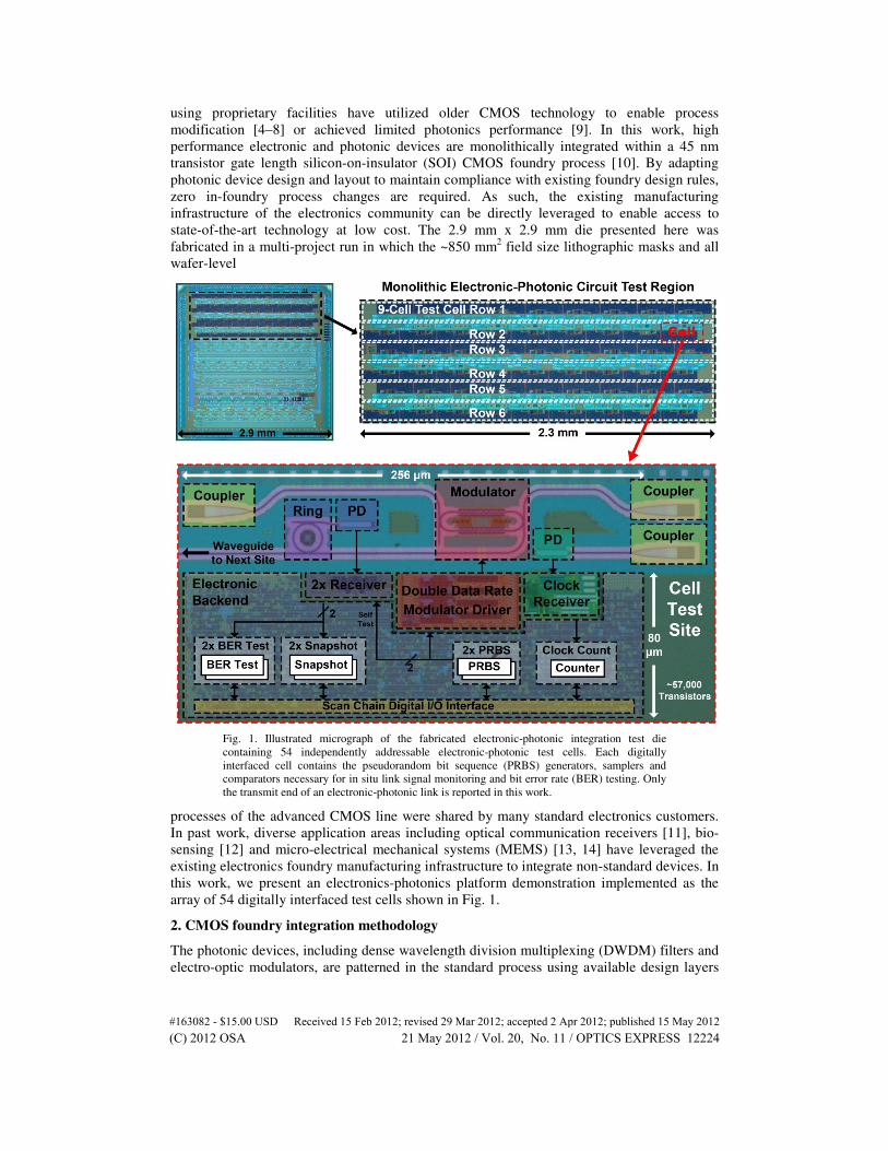
state-of-the-art technology at low cost. The 2.9 mm x 2.9 mm die presented here was
fabricated in a multi-project run in which the ~850 mm2 field size lithographic masks and all
wafer-level
Fig. 1. Illustrated micrograph of the fabricated electronic-photonic integration test die
containing 54 independently addressable electronic-photonic test cells. Each digitally
interfaced cell contains the pseudorandom bit sequence (PRBS) generators, samplers and
comparators necessary for in situ link signal monitoring and bit error rate (BER) testing. Only
the transmit end of an electronic-photonic link is reported in this work.
processes of the advanced CMOS line were shared by many standard electronics customers.
In past work, diverse application areas including optical communication receivers [11], bio-
sensing [12] and micro-electrical mechanical systems (MEMS) [13, 14] have leveraged the
existing electronics foundry manufacturing infrastructure to integrate non-standard devices. In
this work, we present an electronics-photonics platform demonstration implemented as the
array of 54 digitally interfaced test cells shown in Fig. 1.
2. CMOS foundry integration methodology
The photonic devices, including dense wavelength division multiplexing (DWDM) filters and
electro-optic modulators, are patterned in the standard process using available design layers
#163082 - $15.00 USD Received 15 Feb 2012; revised 29 Mar 2012; accepted 2 Apr 2012; published 15 May 2012(C) 2012 OSA 21 May 2012 / Vol. 20, No. 11 / OPTICS EXPRESS 12224
traditionally used for transistor fabrication. Photonic devices were fabricated in the standard
processing flow of the IBM 12SOI 45 nm SOI-CMOS foundry alongside 3-million
transistors. The design was submitted for mask aggregation at the Kansas City Plant (KCP) as
part of a Trusted Access Program Office (TAPO) shuttle run. Physical process details,
including the cross-sectional layer type and thickness information explicitly not reported in
this work, are provided as part of the standard electronic design kit that is made available to
IBM foundry customers under a non-disclosure agreement. A subset of process and
performance information regarding this electronics process can be found in IBM publications
[10,15,16].
Design preparation was performed in Cadence Virtuoso and Encounter tools to enable
electronic-photonic integration and compliant design submission [17]. Local pattern density
process compliance was maintained in mask design while excluding optically-lossy metals
from a 2-3 µm region around the waveguides [17]. Custom auto-fill routines were developed
to identify design coordinates requiring fill to meet pattern density targets using a script
written for Mentor Graphics Calibre. High-density, 0.8 µm x 0.8 µm, metal fill cells were then
automatically inserted at these design coordinates using scripts developed inside Cadence
Virtuoso. Several waivers for violations of standard process design rules were obtained
through the standard foundry infrastructure. Most resulted from photonic devices being
erroneously flagged during the automated design rule check processing as improperly formed
electronic devices. The smooth photonic shapes such as rings and bends were discretized onto
the allowed mask address grid and represented in the submitted database as many rectangles
[17]. Geometry waivers for the small, nanometer-scale notches formed by this discretization
were also obtained, as these shapes have been shown to present no structural threat to process
yield in several process generations from multiple manufacturers [9, 17–19].
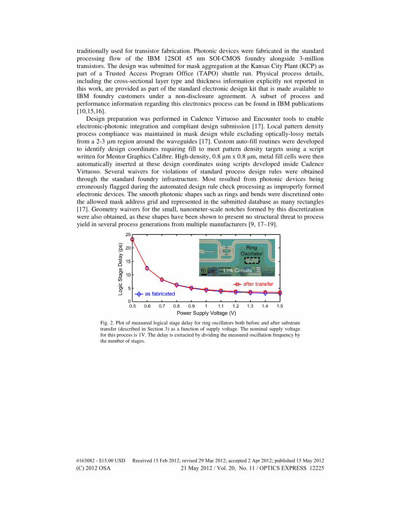
Fig. 2. Plot of measured logical stage delay for ring oscillators both before and after substrate
transfer (described in Section 3) as a function of supply voltage. The nominal supply voltage
for this process is 1V. The delay is extracted by dividing the measured oscillation frequency by
the number of stages.
#163082 - $15.00 USD Received 15 Feb 2012; revised 29 Mar 2012; accepted 2 Apr 2012; published 15 May 2012(C) 2012 OSA 21 May 2012 / Vol. 20, No. 11 / OPTICS EXPRESS 12225
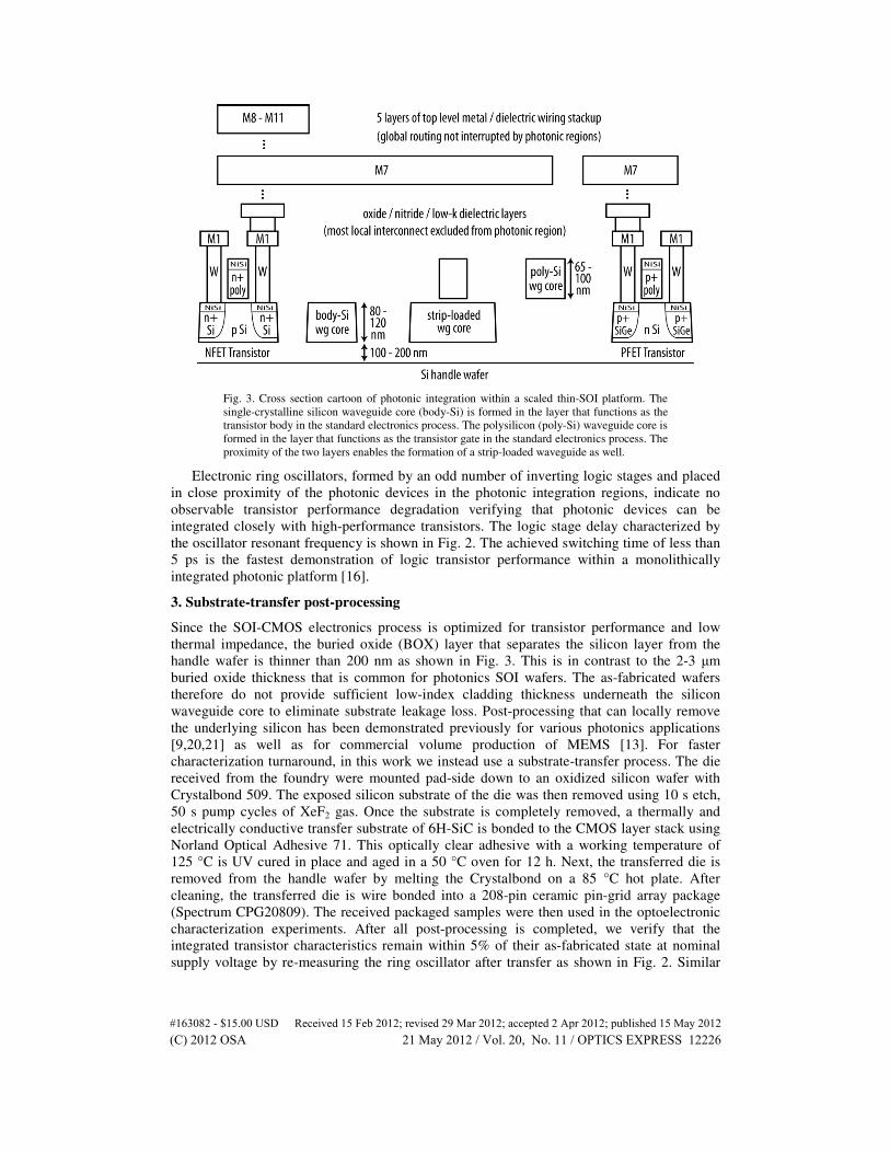
Fig. 3. Cross section cartoon of photonic integration within a scaled thin-SOI platform. The
single-crystalline silicon waveguide core (body-Si) is formed in the layer that functions as the
transistor body in the standard electronics process. The polysilicon (poly-Si) waveguide core is
formed in the layer that functions as the transistor gate in the standard electronics process. The
proximity of the two layers enables the formation of a strip-loaded waveguide as well.
Electronic ring oscillators, formed by an odd number of inverting logic stages and placed
in close proximity of the photonic devices in the photonic integration regions, indicate no
observable transistor performance degradation verifying that photonic devices can be
integrated closely with high-performance transistors. The logic stage delay characterized by
the oscillator resonant frequency is shown in Fig. 2. The achieved switching time of less than
5 ps is the fastest demonstration of logic transistor performance within a monolithically
integrated photonic platform [16].
3. Substrate-transfer post-processing
Since the SOI-CMOS electronics process is optimized for transistor performance and low
thermal impedance, the buried oxide (BOX) layer that separates the silicon layer from the
handle wafer is thinner than 200 nm as shown in Fig. 3. This is in contrast to the 2-3 µm
buried oxide thickness that is common for photonics SOI wafers. The as-fabricated wafers
therefore do not provide sufficient low-index cladding thickness underneath the silicon
waveguide core to eliminate substrate leakage loss. Post-processing that can locally remove
the underlying silicon has been demonstrated previously for various photonics applications
[9,20,21] as well as for commercial volume production of MEMS [13]. For faster
characterization turnaround, in this work we instead use a substrate-transfer process. The die
received from the foundry were mounted pad-side down to an oxidized silicon wafer with
Crystalbond 509. The exposed silicon substrate of the die was then removed using 10 s etch,
50 s pump cycles of XeF2 gas. Once the substrate is completely removed, a thermally and
electrically conductive transfer substrate of 6H-SiC is bonded to the CMOS layer stack using
Norland Optical Adhesive 71. This optically clear adhesive with a working temperature of
125 °C is UV cured in place and aged in a 50 °C oven for 12 h. Next, the transferred die is
removed from the handle wafer by melting the Crystalbond on a 85 °C hot plate. After
cleaning, the transferred die is wire bonded into a 208-pin ceramic pin-grid array package
(Spectrum CPG20809). The received packaged samples were then used in the optoelectronic
characterization experiments. After all post-processing is completed, we verify that the
integrated transistor characteristics remain within 5% of their as-fabricated state at nominal
supply voltage by re-measuring the ring oscillator after transfer as shown in Fig. 2. Similar
#163082 - $15.00 USD Received 15 Feb 2012; revised 29 Mar 2012; accepted 2 Apr 2012; published 15 May 2012(C) 2012 OSA 21 May 2012 / Vol. 20, No. 11 / OPTICS EXPRESS 12226
experiments to verify that wafer-scale, front-side localized substrate removal post-processing
does not impact transistor characteristics have been reported in the post-CMOS MEMS
literature [14].
4. Waveguide loss characterization
To be an enabling technology for a broad range of photonics applications, the integrated
waveguide loss must be comparable to the best available silicon photonics results using
photolithography that are in the range of 2-3 dB/cm for strongly confined modes [22, 23]. In
the SOI-CMOS process, the single-crystalline silicon layer that forms the transistor floating
body may be patterned to form an oxide-clad rectangular waveguide as shown in Fig. 3. This
is in contrast to the previous zero-change integration work in bulk-CMOS [9], where the
polysilicon transistor gate was used. Although the silicon layer thickness of less than 100 nm
and the specific surrounding dielectric environment is unique to the deeply-scaled electronics
process used, the integrated waveguides otherwise closely resemble waveguides from past
electronic integration work [4–8] and photonics-only processes [22, 23]. Previously proposed
optimized silicon waveguide geometries in fact come close to this available ~100 nm
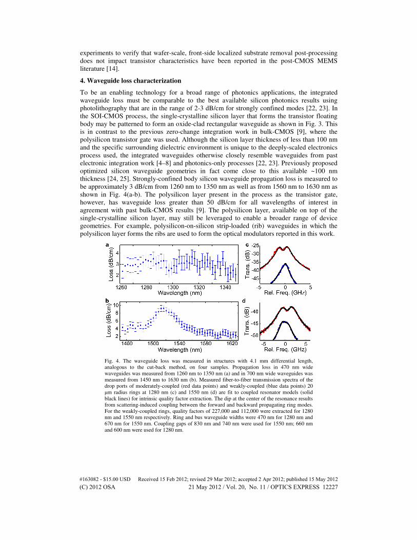
thickness [24, 25]. Strongly-confined body silicon waveguide propagation loss is measured to
be approximately 3 dB/cm from 1260 nm to 1350 nm as well as from 1560 nm to 1630 nm as
shown in Fig. 4(a-b). The polysilicon layer present in the process as the transistor gate,
however, has waveguide loss greater than 50 dB/cm for all wavelengths of interest in
agreement with past bulk-CMOS results [9]. The polysilicon layer, available on top of the
single-crystalline silicon layer, may still be leveraged to enable a broader range of device
geometries. For example, polysilicon-on-silicon strip-loaded (rib) waveguides in which the
polysilicon layer forms the ribs are used to form the optical modulators reported in this work.
Fig. 4. The waveguide loss was measured in structures with 4.1 mm differential length,
analogous to the cut-back method, on four samples. Propagation loss in 470 nm wide
waveguides was measured from 1260 nm to 1350 nm (a) and in 700 nm wide waveguides was
measured from 1450 nm to 1630 nm (b). Measured fiber-to-fiber transmission spectra of the
drop ports of moderately-coupled (red data points) and weakly-coupled (blue data points) 20
µm radius rings at 1280 nm (c) and 1550 nm (d) are fit to coupled resonator models (solid
black lines) for intrinsic quality factor extraction. The dip at the center of the resonance results
from scattering-induced coupling between the forward and backward propagating ring modes.
For the weakly-coupled rings, quality factors of 227,000 and 112,000 were extracted for 1280
nm and 1550 nm respectively. Ring and bus waveguide widths were 470 nm for 1280 nm and
670 nm for 1550 nm. Coupling gaps of 830 nm and 740 nm were used for 1550 nm; 660 nm
and 600 nm were used for 1280 nm.
#163082 - $15.00 USD Received 15 Feb 2012; revised 29 Mar 2012; accepted 2 Apr 2012; published 15 May 2012(C) 2012 OSA 21 May 2012 / Vol. 20, No. 11 / OPTICS EXPRESS 12227
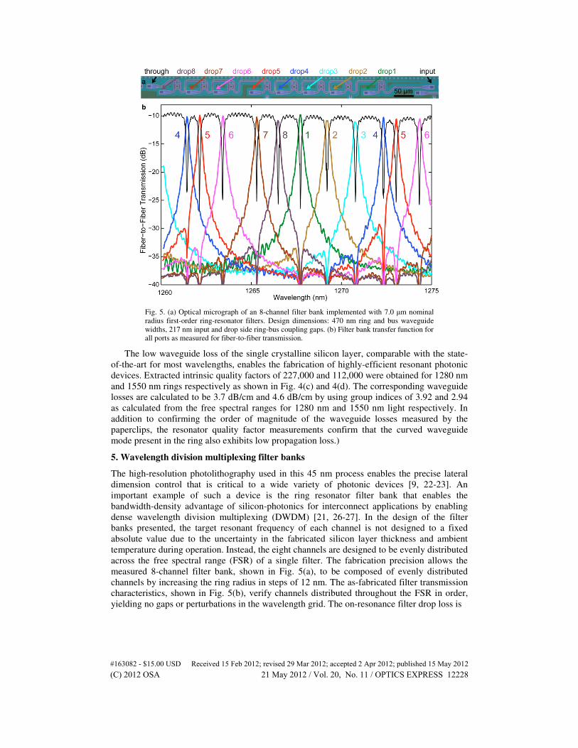
Fig. 5. (a) Optical micrograph of an 8-channel filter bank implemented with 7.0 µm nominal
radius first-order ring-resonator filters. Design dimensions: 470 nm ring and bus waveguide
widths, 217 nm input and drop side ring-bus coupling gaps. (b) Filter bank transfer function for
all ports as measured for fiber-to-fiber transmission.
The low waveguide loss of the single crystalline silicon layer, comparable with the state-
of-the-art for most wavelengths, enables the fabrication of highly-efficient resonant photonic
devices. Extracted intrinsic quality factors of 227,000 and 112,000 were obtained for 1280 nm
and 1550 nm rings respectively as shown in Fig. 4(c) and 4(d). The corresponding waveguide
losses are calculated to be 3.7 dB/cm and 4.6 dB/cm by using group indices of 3.92 and 2.94
as calculated from the free spectral ranges for 1280 nm and 1550 nm light respectively. In
addition to confirming the order of magnitude of the waveguide losses measured by the
paperclips, the resonator quality factor measurements confirm that the curved waveguide
mode present in the ring also exhibits low propagation loss.)
5. Wavelength division multiplexing filter banks
The high-resolution photolithography used in this 45 nm process enables the precise lateral
dimension control that is critical to a wide variety of photonic devices [9, 22-23]. An
important example of such a device is the ring resonator filter bank that enables the
bandwidth-density advantage of silicon-photonics for interconnect applications by enabling
dense wavelength division multiplexing (DWDM) [21, 26-27]. In the design of the filter
banks presented, the target resonant frequency of each channel is not designed to a fixed
absolute value due to the uncertainty in the fabricated silicon layer thickness and ambient
temperature during operation. Instead, the eight channels are designed to be evenly distributed
across the free spectral range (FSR) of a single filter. The fabrication precision allows the
measured 8-channel filter bank, shown in Fig. 5(a), to be composed of evenly distributed
channels by increasing the ring radius in steps of 12 nm. The as-fabricated filter transmission
characteristics, shown in Fig. 5(b), verify channels distributed throughout the FSR in order,
yielding no gaps or perturbations in the wavelength grid. The on-resonance filter drop loss is
#163082 - $15.00 USD Received 15 Feb 2012; revised 29 Mar 2012; accepted 2 Apr 2012; published 15 May 2012(C) 2012 OSA 21 May 2012 / Vol. 20, No. 11 / OPTICS EXPRESS 12228
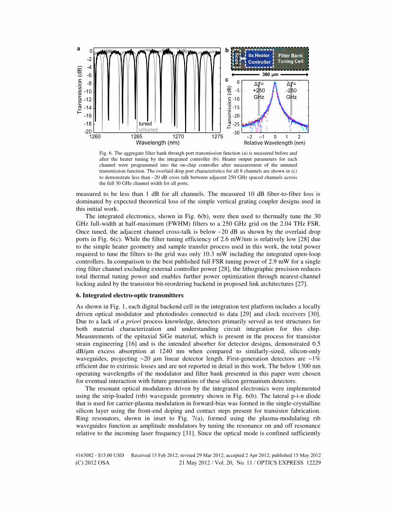
Fig. 6. The aggregate filter bank through port transmission function (a) is measured before and
after the heater tuning by the integrated controller (b). Heater output parameters for each
channel were programmed into the on-chip controller after measurement of the untuned
transmission function. The overlaid drop port characteristics for all 8 channels are shown in (c)
to demonstrate less than −20 dB cross talk between adjacent 250 GHz spaced channels across
the full 30 GHz channel width for all ports.
measured to be less than 1 dB for all channels. The measured 10 dB fiber-to-fiber loss is
dominated by expected theoretical loss of the simple vertical grating coupler designs used in
this initial work.
The integrated electronics, shown in Fig. 6(b), were then used to thermally tune the 30
GHz full-width at half-maximum (FWHM) filters to a 250 GHz grid on the 2.04 THz FSR.
Once tuned, the adjacent channel cross-talk is below −20 dB as shown by the overlaid drop
ports in Fig. 6(c). While the filter tuning efficiency of 2.6 mW/nm is relatively low [28] due
to the simple heater geometry and sample transfer process used in this work, the total power
required to tune the filters to the grid was only 10.3 mW including the integrated open-loop
controllers. In comparison to the best published full FSR tuning power of 2.9 mW for a single
ring filter channel excluding external controller power [28], the lithographic precision reduces
total thermal tuning power and enables further power optimization through nearest-channel
locking aided by the transistor bit-reordering backend in proposed link architectures [27].
6. Integrated electro-optic transmitters
As shown in Fig. 1, each digital backend cell in the integration test platform includes a locally
driven optical modulator and photodiodes connected to data [29] and clock receivers [30].
Due to a lack of a priori process knowledge, detectors primarily served as test structures for
both material characterization and understanding circuit integration for this chip.
Measurements of the epitaxial SiGe material, which is present in the process for transistor
strain engineering [16] and is the intended absorber for detector designs, demonstrated 0.5
dB/µm excess absorption at 1240 nm when compared to similarly-sized, silicon-only
waveguides, projecting ~20 µm linear detector length. First-generation detectors are ~1%
efficient due to extrinsic losses and are not reported in detail in this work. The below 1300 nm
operating wavelengths of the modulator and filter bank presented in this paper were chosen
for eventual interaction with future generations of these silicon germanium detectors.
The resonant optical modulators driven by the integrated electronics were implemented
using the strip-loaded (rib) waveguide geometry shown in Fig. 6(b). The lateral p-i-n diode
that is used for carrier-plasma modulation in forward-bias was formed in the single-crystalline
silicon layer using the front-end doping and contact steps present for transistor fabrication.
Ring resonators, shown in inset to Fig. 7(a), formed using the plasma-modulating rib
waveguides function as amplitude modulators by tuning the resonance on and off resonance
relative to the incoming laser frequency [31]. Since the optical mode is confined sufficiently
#163082 - $15.00 USD Received 15 Feb 2012; revised 29 Mar 2012; accepted 2 Apr 2012; published 15 May 2012(C) 2012 OSA 21 May 2012 / Vol. 20, No. 11 / OPTICS EXPRESS 12229
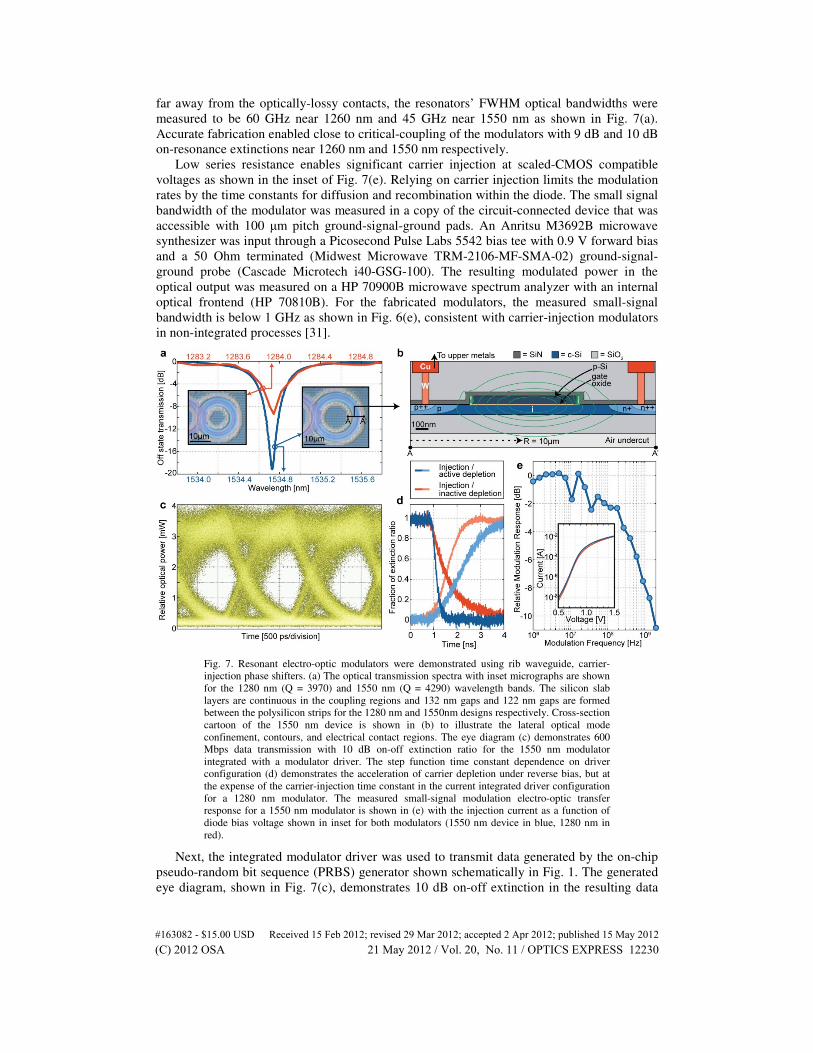
far away from the optically-lossy contacts, the resonators’ FWHM optical bandwidths were
measured to be 60 GHz near 1260 nm and 45 GHz near 1550 nm as shown in Fig. 7(a).
Accurate fabrication enabled close to critical-coupling of the modulators with 9 dB and 10 dB
on-resonance extinctions near 1260 nm and 1550 nm respectively.
Low series resistance enables significant carrier injection at scaled-CMOS compatible
voltages as shown in the inset of Fig. 7(e). Relying on carrier injection limits the modulation
rates by the time constants for diffusion and recombination within the diode. The small signal
bandwidth of the modulator was measured in a copy of the circuit-connected device that was
accessible with 100 µm pitch ground-signal-ground pads. An Anritsu M3692B microwave
synthesizer was input through a Picosecond Pulse Labs 5542 bias tee with 0.9 V forward bias
and a 50 Ohm terminated (Midwest Microwave TRM-2106-MF-SMA-02) ground-signal-
ground probe (Cascade Microtech i40-GSG-100). The resulting modulated power in the
optical output was measured on a HP 70900B microwave spectrum analyzer with an internal
optical frontend (HP 70810B). For the fabricated modulators, the measured small-signal
bandwidth is below 1 GHz as shown in Fig. 6(e), consistent with carrier-injection modulators
in non-integrated processes [31].
Fig. 7. Resonant electro-optic modulators were demonstrated using rib waveguide, carrier-
injection phase shifters. (a) The optical transmission spectra with inset micrographs are shown
for the 1280 nm (Q = 3970) and 1550 nm (Q = 4290) wavelength bands. The silicon slab
layers are continuous in the coupling regions and 132 nm gaps and 122 nm gaps are formed
between the polysilicon strips for the 1280 nm and 1550nm designs respectively. Cross-section
cartoon of the 1550 nm device is shown in (b) to illustrate the lateral optical mode
confinement, contours, and electrical contact regions. The eye diagram (c) demonstrates 600
Mbps data transmission with 10 dB on-off extinction ratio for the 1550 nm modulator
integrated with a modulator driver. The step function time constant dependence on driver
configuration (d) demonstrates the acceleration of carrier depletion under reverse bias, but at
the expense of the carrier-injection time constant in the current integrated driver configuration
for a 1280 nm modulator. The measured small-signal modulation electro-optic transfer
response for a 1550 nm modulator is shown in (e) with the injection current as a function of
diode bias voltage shown in inset for both modulators (1550 nm device in blue, 1280 nm in
red).
Next, the integrated modulator driver was used to transmit data generated by the on-chip
pseudo-random bit sequence (PRBS) generator shown schematically in Fig. 1. The generated
eye diagram, shown in Fig. 7(c), demonstrates 10 dB on-off extinction in the resulting data
#163082 - $15.00 USD Received 15 Feb 2012; revised 29 Mar 2012; accepted 2 Apr 2012; published 15 May 2012(C) 2012 OSA 21 May 2012 / Vol. 20, No. 11 / OPTICS EXPRESS 12230
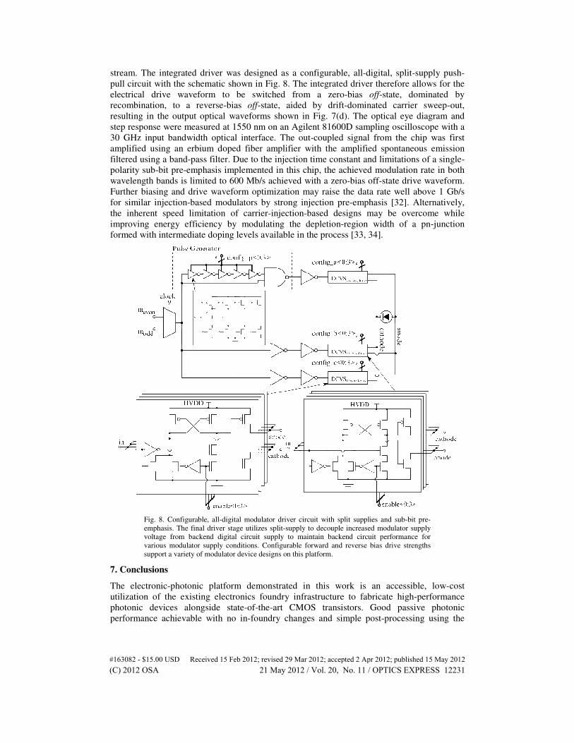
stream. The integrated driver was designed as a configurable, all-digital, split-supply push-
pull circuit with the schematic shown in Fig. 8. The integrated driver therefore allows for the
electrical drive waveform to be switched from a zero-bias off-state, dominated by
recombination, to a reverse-bias off-state, aided by drift-dominated carrier sweep-out,
resulting in the output optical waveforms shown in Fig. 7(d). The optical eye diagram and
step response were measured at 1550 nm on an Agilent 81600D sampling oscilloscope with a
30 GHz input bandwidth optical interface. The out-coupled signal from the chip was first
amplified using an erbium doped fiber amplifier with the amplified spontaneous emission
filtered using a band-pass filter. Due to the injection time constant and limitations of a single-
polarity sub-bit pre-emphasis implemented in this chip, the achieved modulation rate in both
wavelength bands is limited to 600 Mb/s achieved with a zero-bias off-state drive waveform.
Further biasing and drive waveform optimization may raise the data rate well above 1 Gb/s
for similar injection-based modulators by strong injection pre-emphasis [32]. Alternatively,
the inherent speed limitation of carrier-injection-based designs may be overcome while
improving energy efficiency by modulating the depletion-region width of a pn-junction
formed with intermediate doping levels available in the process [33, 34].
Fig. 8. Configurable, all-digital modulator driver circuit with split supplies and sub-bit pre-
emphasis. The final driver stage utilizes split-supply to decouple increased modulator supply
voltage from backend digital circuit supply to maintain backend circuit performance for
various modulator supply conditions. Configurable forward and reverse bias drive strengths
support a variety of modulator device designs on this platform.
7. Conclusions
The electronic-photonic platform demonstrated in this work is an accessible, low-cost
utilization of the existing electronics foundry infrastructure to fabricate high-performance
photonic devices alongside state-of-the-art CMOS transistors. Good passive photonic
performance achievable with no in-foundry changes and simple post-processing using the
#163082 - $15.00 USD Received 15 Feb 2012; revised 29 Mar 2012; accepted 2 Apr 2012; published 15 May 2012(C) 2012 OSA 21 May 2012 / Vol. 20, No. 11 / OPTICS EXPRESS 12231

thin-SOI-CMOS process removes the waveguide loss bottleneck present in previous work [9].
Devices such as the filter bank demultiplexer and modulator presented in this work, together
with integrated photodetectors that are currently under development, form the basis of a
photonic interconnect platform in an advanced electronics process that is used to fabricate
microprocessors today [15]. The general-purpose nature of this foundry platform provides
access to state-of-the-art technology that will greatly empower research into novel electro-
optic systems-on-chip across the entire spectrum of VLSI and photonic systems and
applications.
Acknowledgments
This work was funded by DARPA award W911NF-10-1-0412, and also in part by the NSF,
the FCRP IFC, MIT CICS, and the Trusted Foundry. The views expressed are those of the
authors and do not reflect the official policy or position of the Department of Defense or the
U.S. Government.
#163082 - $15.00 USD Received 15 Feb 2012; revised 29 Mar 2012; accepted 2 Apr 2012; published 15 May 2012(C) 2012 OSA 21 May 2012 / Vol. 20, No. 11 / OPTICS EXPRESS 12232