Embed Size (px)
Citation preview
To link to this article: DOI: 10.1088/0957-4484/23/1/015603 URL: http://dx.doi.org/10.1088/0957-4484/23/1/015603
This is an author-deposited version published in: http://oatao.univ-toulouse.fr/ Eprints ID: 5452
To cite this version: Bedel, Laurent and Cayron, Cyril and Jouve, Michel and Maury, Francis Embedded layer of Ag nanoparticles prepared by a combined PECVD/PVD process producing SiOxCy-Ag nanocomposite thin films. (2012) Nanotechnology, vol. 23 (n° 1). p. 015603(1) -015603(8). ISSN 1361-6528
Open Archive Toulouse Archive Ouverte (OATAO) OATAO is an open access repository that collects the work of Toulouse researchers and makes it freely available over the web where possible.
Any correspondence concerning this service should be sent to the repository administrator: [email protected]
doi:10.1088/0957-4484/23/1/015603
Embedded layer of Ag nanoparticlesprepared by a combined PECVD/PVDprocess producing SiOxCy–Agnanocomposite thin films
Laurent Bedel1, Cyril Cayron2, Michel Jouve1 and Francis Maury3
1 CEA, LITEN, DTNM, LTS, 17, rue des martyrs 38054 Grenoble, France2 CEA, LITEN, DEHT, LCPEM, Minatec, 17, rue des martyrs 38054 Grenoble, France3 CIRIMAT, CNRS/INPT/UPS, ENSIACET, 4 allee E Monso, BP 44362,
31030 Toulouse cedex 4, France
E-mail: [email protected]
Abstract
Structural properties of SiOxCy–Ag nanocomposite thin films prepared by a dual process
PVD–PECVD in the same reactor have been investigated. The experimental results have
demonstrated the influence of a PECVD process carried out at room temperature for the growth
of a dielectric matrix on the size and the distribution density of Ag nanoparticles (NPs)
deposited beforehand by magnetron sputtering. The plasma during the growth of the
encapsulation SiOxCy layer caused a diffusion of silver from NPs through the SiOxCy matrix
associated with a decrease in the average size of nanoparticles and an increase of their
distribution density. Silver diffusion is blocked at a barrier interface to form a buried layer of
individual Ag NPs which, for instance, can find plasmonic applications. Silver also diffuses
toward the outer surface inducing antibacterial properties. In both cases initial Ag NPs act as
reservoirs for multifunctional properties of advanced nanostructured films.
1. Introduction
Nanocomposite thin films constituted of metallic nanoparticles
(NPs) embedded in a dielectric matrix are of increasing
interest in many application fields such as solar cells [1, 2],
sensors [3, 4] and optical devices due to their remarkable
properties. The presence of nanoparticles improves light
absorption due to surface plasmons [5, 6]. One of the
main issues of the growth processes of these coatings is to
control the nanostructuration that is essential to obtain the
desired functional properties, i.e. the size, the shape and the
distribution density of the metal NPs. Such films can be
elaborated by vapor deposition processes [7, 8] either in one
step [9, 10] or multi-step processes [11].
In one step processes, the growth of the matrix and
metallic NPs occurs simultaneously and the size, the shape
and the distribution density of nanoparticles depend on the
process parameters. Generally, the metallic NPs are uniformly
distributed throughout the thickness of the nanocomposite film.
Even using a related vapor phase deposition process, the size
of metallic NPs depends on the nature of the metal. Their size
distribution can be monodisperse as reported for TiO2–Ag [12]
or significantly broader as for TiO2–Cu [13]. Multi-step
processes are a second route to produce nanocomposite films.
Generally the architecture is based on multilayer structures.
After the deposition of a controlled size and density of metal
NPs, a dielectric thin film covers them. However, in this
approach, the growth of the dielectric layer can affect the
shape, the size and the density of nanoparticles. For instance,
Simonet et al [11] have detected silver NPs reshaping after
the growth of a Si3N4 encapsulation layer. The shape is also
affected by the nature of the sublayer and of the top layer on
Ag NPs [14].
In this work, structural properties of SiOxCy–Ag
nanocomposite thin films prepared by a dual process in the
same reactor have been investigated. The influence of the
growth of the SiOxCy matrix deposited by plasma enhanced
chemical vapor deposition (PECVD) onto Ag nanoparticles
deposited by the magnetron sputtering process (physical vapor
deposition, PVD) has been studied. The plasma during the
growth of the encapsulation SiOxCy layer induces a diffusion
of silver and significant changes in the average size and
distribution density of Ag NPs. Nanoparticles can be pinned
at a barrier interface to form a layer of individual metal NPs
with a good control of their shape and their nanoscale size.
2. Experimental details
2.1. Coating deposition
The SiOxCy–Ag nanocomposite thin films were grown at room
temperature in three steps, in the same deposition chamber,
i.e. without atmospheric contamination of the samples between
each step. The first and third stages consisted of the deposition
of SiOxCy layers acting as dielectric matrix and the second
one of the deposition of silver NPs. The nanostructured films
were deposited on various substrates including borosilicate
glass, Si wafer and copper grid with a thin film of carbon for
transmission electron microscopy (TEM) direct analyses.
PECVD and PVD modules are implemented in the same
reactor. The substrates are fixed on a stainless steel rotating
cylindrical sample holder alternately passing in front of each
depositing unit. This sequential process is adapted for the
growth of multilayer nanostructures. The reactor size is
approximately 90 × 75 × 55 cm3 and the diameter of the
metallic sample holder is 65 cm. The two deposition modules
are separated by 20 cm and the rotating speed was 1.66 cm s−1.
There is no heating system of the substrates and the deposition
occurs at room temperature or close to it. So this reactor
was also used for continuous coating on polymer supports
without degradation of such thermally sensitive materials
(unpublished).
The SiOxCy matrix was deposited by PECVD at a
constant pressure of 26 Pa. A mixture of He and
hexamethyldisiloxane (HMDSO) precursor (1%) was injected
into the reactor as reactive gas phase. All the SiOxCy films
were grown using low frequency plasma excitation (40 kHz)
and a power density of 0.64 W cm−2 in a capacitive parallel
plate (space 4 cm) configuration. The deposition time was
fixed at 10 s. This run corresponds to one cycle and under
these growth conditions the SiOxCy thickness is about 30 nm.
The second stage consisted of the deposition of Ag
nanoparticles by pulsed magnetron sputtering at a constant
pressure of about 26 Pa as well. The silver target was located
at 3.5 cm distance from the substrate holder. Argon was used
as sputtering gas and the power density on the silver target was
fixed either at 0.7 or 1.4 W cm−2 depending on the number of
Ag NPs required. The NPs’ deposition time was fixed at 7 s
and the pulse frequency was set at 100 kHz. A vacuum purge
was carried out between each step to evacuate the atmosphere
of the previous step using a roots pump.
In preliminary runs, the growth of SiOxCy/Ag/SiOxCy
nanocomposite films was interrupted at every step, i.e. the
reactor was opened between each step to wrap the silver target
or the PECVD cathode in an aluminum foil to avoid possible
Ag contamination during the deposition of the sandwiched
dielectric layer. Because no significant difference was found
with the deposition sequence described above, i.e. the steps
were chained in sequence without opening the reactor to the
atmosphere, this procedure was further adopted.
2.2. Characterization of thin films
The films grown on Si substrates were used to analyze
the composition and the element distribution throughout the
thickness of the films. X-ray photoelectron spectroscopy
(XPS) was performed using a VG Escalab MKII spec-
trophotometer, which operated with a non-monochromatized
Mg Kα source (1253.6 eV). The XPS composition profiles
were determined by analyzing the surface after several Ar+
sputtering sequences. The elements were analyzed using the
core levels Si 2p, O 1s, C 1s and Ag 3d. However, the Ag 3d
signal was not always detected or its intensity was too low to be
extracted from the background for quantification. Secondary
ion mass spectrometry (SIMS) using a CAMECA IMS 4F6
analyzer (Cs+ bombardment) was also used to determine
the element distribution throughout the film thickness with a
higher depth resolution.
The size and the distribution density of Ag NPs were
determined by transmission electron microscopy (TEM). The
silver NPs deposited after the first and the second SiOxCy layer
on copper grids covered by a thin carbon film were used to
determine their size and the density in the same conditions
as those used for the deposition onto silicon substrates. The
size distribution and the densities of the silver NPs were
measured with the image analysis software ImageJ. Moreover,
in order to observe the distribution of silver NPs in films
and to avoid possible charging effects, cross sectional samples
were prepared on films grown on Si specimens. The cross-
section TEM samples were prepared by mechanical tripod
polishing on the MultiPrep system (Allied equipment). Ion
milling and focus ion beam techniques were not used because
such methods modify the Ag NPs’ distribution. The TEM
investigations were carried out on a conventional Jeol 2000FX
TEM at 200 kV and on a probe Cs-corrected FEI Titan TEM
operating at 300 kV in high resolution scanning transmission
(HRSTEM) mode with bright field (BF) and in high angle
annular dark field (HAADF) detectors.
The optical properties of films deposited on borosilicate
glass samples were analyzed using a Perkin Elmer Lambda
950 apparatus. The transmittance was determined in the
wavelength range from 200 to 800 nm.
3. Results
3.1. Size and distribution density of Ag NPs
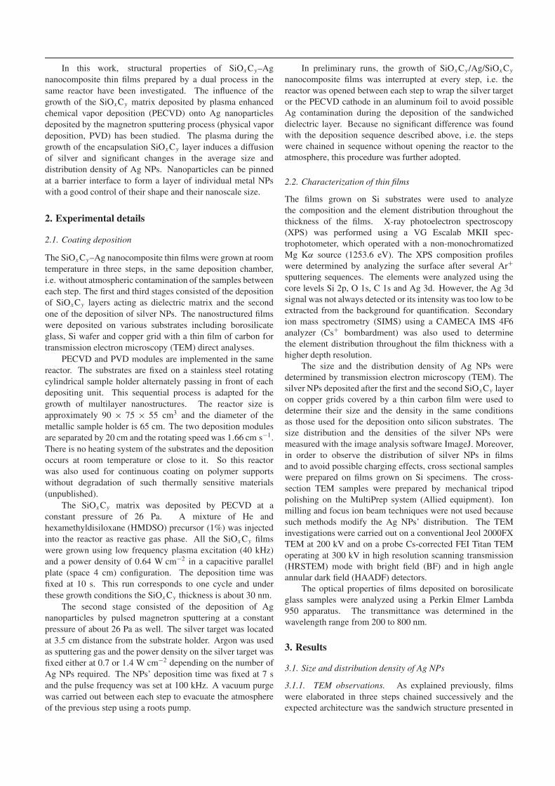
3.1.1. TEM observations. As explained previously, films
were elaborated in three steps chained successively and the
expected architecture was the sandwich structure presented in
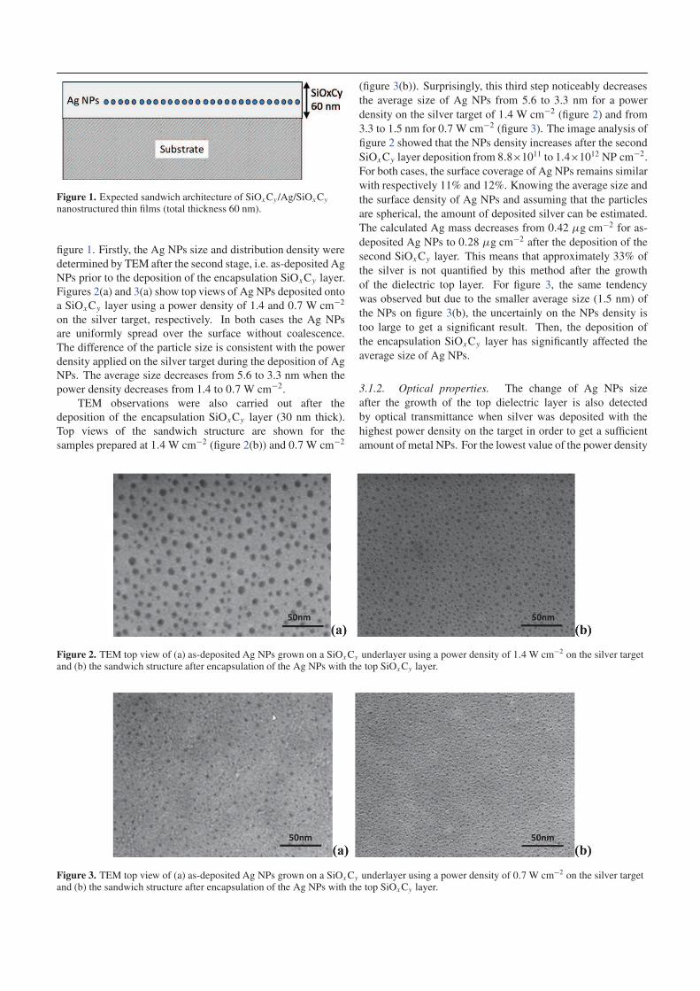
Figure 1. Expected sandwich architecture of SiOxCy /Ag/SiOxCy
nanostructured thin films (total thickness 60 nm).
figure 1. Firstly, the Ag NPs size and distribution density were
determined by TEM after the second stage, i.e. as-deposited Ag
NPs prior to the deposition of the encapsulation SiOxCy layer.
Figures 2(a) and 3(a) show top views of Ag NPs deposited onto
a SiOxCy layer using a power density of 1.4 and 0.7 W cm−2
on the silver target, respectively. In both cases the Ag NPs
are uniformly spread over the surface without coalescence.
The difference of the particle size is consistent with the power
density applied on the silver target during the deposition of Ag
NPs. The average size decreases from 5.6 to 3.3 nm when the
power density decreases from 1.4 to 0.7 W cm−2.
TEM observations were also carried out after the
deposition of the encapsulation SiOxCy layer (30 nm thick).
Top views of the sandwich structure are shown for the
samples prepared at 1.4 W cm−2 (figure 2(b)) and 0.7 W cm−2
(figure 3(b)). Surprisingly, this third step noticeably decreases
the average size of Ag NPs from 5.6 to 3.3 nm for a power
density on the silver target of 1.4 W cm−2 (figure 2) and from
3.3 to 1.5 nm for 0.7 W cm−2 (figure 3). The image analysis of
figure 2 showed that the NPs density increases after the second
SiOxCy layer deposition from 8.8×10¹¹ to 1.4×10¹² NP cm−2.
For both cases, the surface coverage of Ag NPs remains similar
with respectively 11% and 12%. Knowing the average size and
the surface density of Ag NPs and assuming that the particles
are spherical, the amount of deposited silver can be estimated.
The calculated Ag mass decreases from 0.42 µg cm−2 for as-
deposited Ag NPs to 0.28 µg cm−2 after the deposition of the
second SiOxCy layer. This means that approximately 33% of
the silver is not quantified by this method after the growth
of the dielectric top layer. For figure 3, the same tendency
was observed but due to the smaller average size (1.5 nm) of
the NPs on figure 3(b), the uncertainly on the NPs density is
too large to get a significant result. Then, the deposition of
the encapsulation SiOxCy layer has significantly affected the
average size of Ag NPs.
3.1.2. Optical properties. The change of Ag NPs size
after the growth of the top dielectric layer is also detected
by optical transmittance when silver was deposited with the
highest power density on the target in order to get a sufficient
amount of metal NPs. For the lowest value of the power density
Figure 2. TEM top view of (a) as-deposited Ag NPs grown on a SiOxCy underlayer using a power density of 1.4 W cm−2 on the silver targetand (b) the sandwich structure after encapsulation of the Ag NPs with the top SiOxCy layer.
Figure 3. TEM top view of (a) as-deposited Ag NPs grown on a SiOxCy underlayer using a power density of 0.7 W cm−2 on the silver targetand (b) the sandwich structure after encapsulation of the Ag NPs with the top SiOxCy layer.
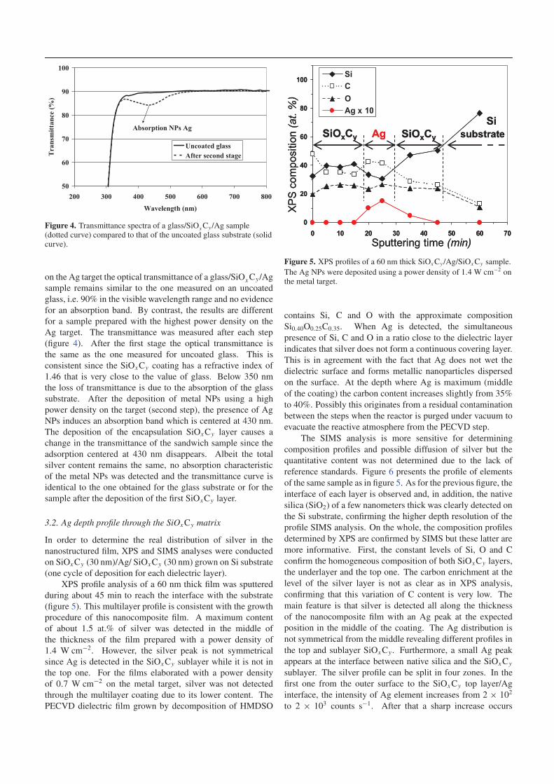
Figure 4. Transmittance spectra of a glass/SiOxCy /Ag sample(dotted curve) compared to that of the uncoated glass substrate (solidcurve).
on the Ag target the optical transmittance of a glass/SiOxCy/Ag
sample remains similar to the one measured on an uncoated
glass, i.e. 90% in the visible wavelength range and no evidence
for an absorption band. By contrast, the results are different
for a sample prepared with the highest power density on the
Ag target. The transmittance was measured after each step
(figure 4). After the first stage the optical transmittance is
the same as the one measured for uncoated glass. This is
consistent since the SiOxCy coating has a refractive index of
1.46 that is very close to the value of glass. Below 350 nm
the loss of transmittance is due to the absorption of the glass
substrate. After the deposition of metal NPs using a high
power density on the target (second step), the presence of Ag
NPs induces an absorption band which is centered at 430 nm.
The deposition of the encapsulation SiOxCy layer causes a
change in the transmittance of the sandwich sample since the
adsorption centered at 430 nm disappears. Albeit the total
silver content remains the same, no absorption characteristic
of the metal NPs was detected and the transmittance curve is
identical to the one obtained for the glass substrate or for the
sample after the deposition of the first SiOxCy layer.
3.2. Ag depth profile through the SiOxCy matrix
In order to determine the real distribution of silver in the
nanostructured film, XPS and SIMS analyses were conducted
on SiOxCy (30 nm)/Ag/ SiOxCy (30 nm) grown on Si substrate
(one cycle of deposition for each dielectric layer).
XPS profile analysis of a 60 nm thick film was sputtered
during about 45 min to reach the interface with the substrate
(figure 5). This multilayer profile is consistent with the growth
procedure of this nanocomposite film. A maximum content
of about 1.5 at.% of silver was detected in the middle of
the thickness of the film prepared with a power density of
1.4 W cm−2. However, the silver peak is not symmetrical
since Ag is detected in the SiOxCy sublayer while it is not in
the top one. For the films elaborated with a power density
of 0.7 W cm−2 on the metal target, silver was not detected
through the multilayer coating due to its lower content. The
PECVD dielectric film grown by decomposition of HMDSO
Figure 5. XPS profiles of a 60 nm thick SiOxCy /Ag/SiOxCy sample.
The Ag NPs were deposited using a power density of 1.4 W cm−2 onthe metal target.
contains Si, C and O with the approximate composition
Si0.40O0.25C0.35. When Ag is detected, the simultaneous
presence of Si, C and O in a ratio close to the dielectric layer
indicates that silver does not form a continuous covering layer.
This is in agreement with the fact that Ag does not wet the
dielectric surface and forms metallic nanoparticles dispersed
on the surface. At the depth where Ag is maximum (middle
of the coating) the carbon content increases slightly from 35%
to 40%. Possibly this originates from a residual contamination
between the steps when the reactor is purged under vacuum to
evacuate the reactive atmosphere from the PECVD step.
The SIMS analysis is more sensitive for determining
composition profiles and possible diffusion of silver but the
quantitative content was not determined due to the lack of
reference standards. Figure 6 presents the profile of elements
of the same sample as in figure 5. As for the previous figure, the
interface of each layer is observed and, in addition, the native
silica (SiO2) of a few nanometers thick was clearly detected on
the Si substrate, confirming the higher depth resolution of the
profile SIMS analysis. On the whole, the composition profiles
determined by XPS are confirmed by SIMS but these latter are
more informative. First, the constant levels of Si, O and C
confirm the homogeneous composition of both SiOxCy layers,
the underlayer and the top one. The carbon enrichment at the
level of the silver layer is not as clear as in XPS analysis,
confirming that this variation of C content is very low. The
main feature is that silver is detected all along the thickness
of the nanocomposite film with an Ag peak at the expected
position in the middle of the coating. The Ag distribution is
not symmetrical from the middle revealing different profiles in
the top and sublayer SiOxCy . Furthermore, a small Ag peak
appears at the interface between native silica and the SiOxCy
sublayer. The silver profile can be split in four zones. In the
first one from the outer surface to the SiOxCy top layer/Ag
interface, the intensity of Ag element increases from 2 × 10²
to 2 × 10³ counts s−1. After that a sharp increase occurs
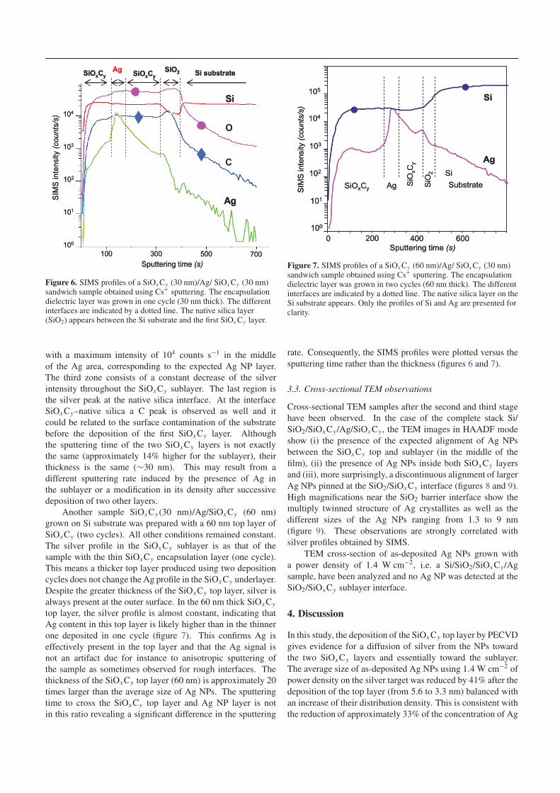
Figure 6. SIMS profiles of a SiOxCy (30 nm)/Ag/ SiOxCy (30 nm)sandwich sample obtained using Cs+ sputtering. The encapsulationdielectric layer was grown in one cycle (30 nm thick). The differentinterfaces are indicated by a dotted line. The native silica layer(SiO2) appears between the Si substrate and the first SiOxCy layer.
with a maximum intensity of 104 counts s−1 in the middle
of the Ag area, corresponding to the expected Ag NP layer.
The third zone consists of a constant decrease of the silver
intensity throughout the SiOxCy sublayer. The last region is
the silver peak at the native silica interface. At the interface
SiOxCy–native silica a C peak is observed as well and it
could be related to the surface contamination of the substrate
before the deposition of the first SiOxCy layer. Although
the sputtering time of the two SiOxCy layers is not exactly
the same (approximately 14% higher for the sublayer), their
thickness is the same (∼30 nm). This may result from a
different sputtering rate induced by the presence of Ag in
the sublayer or a modification in its density after successive
deposition of two other layers.
Another sample SiOxCy(30 nm)/Ag/SiOxCy (60 nm)
grown on Si substrate was prepared with a 60 nm top layer of
SiOxCy (two cycles). All other conditions remained constant.
The silver profile in the SiOxCy sublayer is as that of the
sample with the thin SiOxCy encapsulation layer (one cycle).
This means a thicker top layer produced using two deposition
cycles does not change the Ag profile in the SiOxCy underlayer.
Despite the greater thickness of the SiOxCy top layer, silver is
always present at the outer surface. In the 60 nm thick SiOxCy
top layer, the silver profile is almost constant, indicating that
Ag content in this top layer is likely higher than in the thinner
one deposited in one cycle (figure 7). This confirms Ag is
effectively present in the top layer and that the Ag signal is
not an artifact due for instance to anisotropic sputtering of
the sample as sometimes observed for rough interfaces. The
thickness of the SiOxCy top layer (60 nm) is approximately 20
times larger than the average size of Ag NPs. The sputtering
time to cross the SiOxCy top layer and Ag NP layer is not
in this ratio revealing a significant difference in the sputtering
Figure 7. SIMS profiles of a SiOxCy (60 nm)/Ag/ SiOxCy (30 nm)sandwich sample obtained using Cs+ sputtering. The encapsulationdielectric layer was grown in two cycles (60 nm thick). The differentinterfaces are indicated by a dotted line. The native silica layer on theSi substrate appears. Only the profiles of Si and Ag are presented forclarity.
rate. Consequently, the SIMS profiles were plotted versus the
sputtering time rather than the thickness (figures 6 and 7).
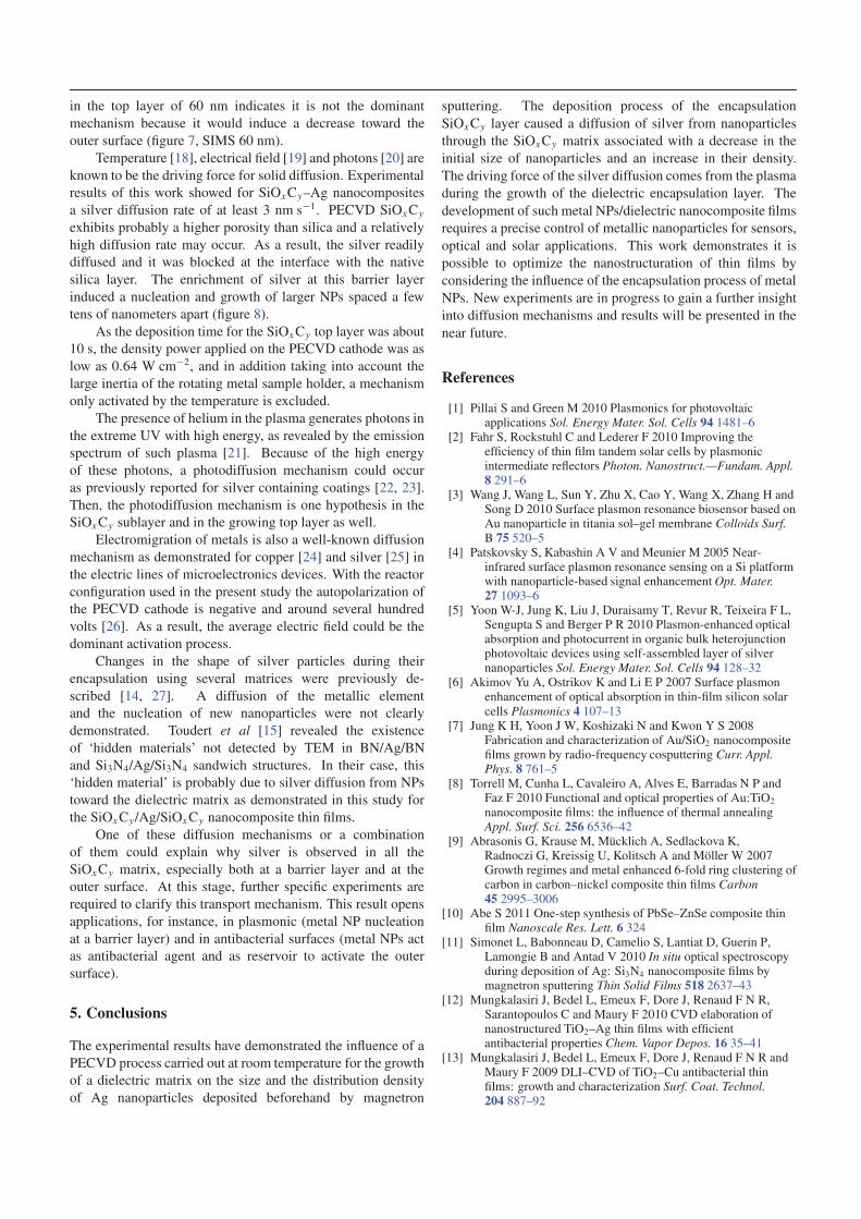
3.3. Cross-sectional TEM observations
Cross-sectional TEM samples after the second and third stage
have been observed. In the case of the complete stack Si/
SiO2/SiOxCy /Ag/SiOxCy , the TEM images in HAADF mode
show (i) the presence of the expected alignment of Ag NPs
between the SiOxCy top and sublayer (in the middle of the
film), (ii) the presence of Ag NPs inside both SiOxCy layers
and (iii), more surprisingly, a discontinuous alignment of larger
Ag NPs pinned at the SiO2/SiOxCy interface (figures 8 and 9).
High magnifications near the SiO2 barrier interface show the
multiply twinned structure of Ag crystallites as well as the
different sizes of the Ag NPs ranging from 1.3 to 9 nm
(figure 9). These observations are strongly correlated with
silver profiles obtained by SIMS.
TEM cross-section of as-deposited Ag NPs grown with
a power density of 1.4 W cm−2, i.e. a Si/SiO2/SiOxCy/Ag
sample, have been analyzed and no Ag NP was detected at the
SiO2/SiOxCy sublayer interface.
4. Discussion
In this study, the deposition of the SiOxCy top layer by PECVD
gives evidence for a diffusion of silver from the NPs toward
the two SiOxCy layers and essentially toward the sublayer.
The average size of as-deposited Ag NPs using 1.4 W cm−2 of
power density on the silver target was reduced by 41% after the
deposition of the top layer (from 5.6 to 3.3 nm) balanced with
an increase of their distribution density. This is consistent with
the reduction of approximately 33% of the concentration of Ag
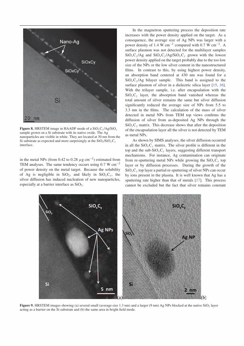
Figure 8. HRSTEM image in HAADF mode of a SiOxCy /Ag/SiOx
sample grown on a Si substrate with its native oxide. The Agnanoparticles are visible in white. They are located at 30 nm from theSi substrate as expected and more surprisingly at the SiO2/SiOxCy
interface.
in the metal NPs (from 0.42 to 0.28 µg cm−2) estimated from
TEM analyses. The same tendency occurs using 0.7 W cm−2
of power density on the metal target. Because the solubility
of Ag is negligible in SiO2, and likely in SiOxCy , the
silver diffusion has induced nucleation of new nanoparticles,
especially at a barrier interface as SiO2.
In the magnetron sputtering process the deposition rate
increases with the power density applied on the target. As a
consequence, the average size of Ag NPs was larger with a
power density of 1.4 W cm−2 compared with 0.7 W cm−2. A
surface plasmon was not detected for the multilayer samples
SiOxCy/Ag and SiOxCy/Ag/SiOxCy grown with the lowest
power density applied on the target probably due to the too low
size of the NPs or the low silver content in the nanostructured
films. In contrast to this, by using highest power density,
an absorption band centered at 430 nm was found for a
SiOxCy/Ag bilayer sample. This band is assigned to the
surface plasmon of silver in a dielectric silica layer [15, 16].
With the trilayer sample, i.e. after encapsulation with the
SiOxCy layer, the absorption band vanished whereas the
total amount of silver remains the same but silver diffusion
significantly reduced the average size of NPs from 5.5 to
3.3 nm in the films. The calculation of the mass of silver
detected in metal NPs from TEM top views confirms the
diffusion of silver from as-deposited Ag NPs through the
SiOxCy matrix. This decrease shows that after the deposition
of the encapsulation layer all the silver is not detected by TEM
as metal NPs.
As shown by SIMS analyses, the silver diffusion occurred
in all the SiOxCy matrix. The silver profile is different in the
top and the sub-SiOxCy layers, suggesting different transport
mechanisms. For instance, Ag contamination can originate
from re-sputtering metal NPs while growing the SiOxCy top
layer or by diffusion processes. During the growth of the
SiOxCy top layer a partial re-sputtering of silver NPs can occur
by ions present in the plasma. It is well known that Ag has a
sputtering rate higher than that of metals [17]. This process
cannot be excluded but the fact that silver remains constant
Figure 9. HRSTEM images showing (a) several small (average size 1.3 nm) and a larger (9 nm) Ag NPs blocked at the native SiO2 layeracting as a barrier on the Si substrate and (b) the same area in bright field mode.
in the top layer of 60 nm indicates it is not the dominant
mechanism because it would induce a decrease toward the
outer surface (figure 7, SIMS 60 nm).
Temperature [18], electrical field [19] and photons [20] are
known to be the driving force for solid diffusion. Experimental
results of this work showed for SiOxCy–Ag nanocomposites
a silver diffusion rate of at least 3 nm s−1. PECVD SiOxCy
exhibits probably a higher porosity than silica and a relatively
high diffusion rate may occur. As a result, the silver readily
diffused and it was blocked at the interface with the native
silica layer. The enrichment of silver at this barrier layer
induced a nucleation and growth of larger NPs spaced a few
tens of nanometers apart (figure 8).
As the deposition time for the SiOxCy top layer was about
10 s, the density power applied on the PECVD cathode was as
low as 0.64 W cm−2, and in addition taking into account the
large inertia of the rotating metal sample holder, a mechanism
only activated by the temperature is excluded.
The presence of helium in the plasma generates photons in
the extreme UV with high energy, as revealed by the emission
spectrum of such plasma [21]. Because of the high energy
of these photons, a photodiffusion mechanism could occur
as previously reported for silver containing coatings [22, 23].
Then, the photodiffusion mechanism is one hypothesis in the
SiOxCy sublayer and in the growing top layer as well.
Electromigration of metals is also a well-known diffusion
mechanism as demonstrated for copper [24] and silver [25] in
the electric lines of microelectronics devices. With the reactor
configuration used in the present study the autopolarization of
the PECVD cathode is negative and around several hundred
volts [26]. As a result, the average electric field could be the
dominant activation process.
Changes in the shape of silver particles during their
encapsulation using several matrices were previously de-
scribed [14, 27]. A diffusion of the metallic element
and the nucleation of new nanoparticles were not clearly
demonstrated. Toudert et al [15] revealed the existence
of ‘hidden materials’ not detected by TEM in BN/Ag/BN
and Si3N4/Ag/Si3N4 sandwich structures. In their case, this
‘hidden material’ is probably due to silver diffusion from NPs
toward the dielectric matrix as demonstrated in this study for
the SiOxCy/Ag/SiOxCy nanocomposite thin films.
One of these diffusion mechanisms or a combination
of them could explain why silver is observed in all the
SiOxCy matrix, especially both at a barrier layer and at the
outer surface. At this stage, further specific experiments are
required to clarify this transport mechanism. This result opens
applications, for instance, in plasmonic (metal NP nucleation
at a barrier layer) and in antibacterial surfaces (metal NPs act
as antibacterial agent and as reservoir to activate the outer
surface).
5. Conclusions
The experimental results have demonstrated the influence of a
PECVD process carried out at room temperature for the growth
of a dielectric matrix on the size and the distribution density
of Ag nanoparticles deposited beforehand by magnetron
sputtering. The deposition process of the encapsulation
SiOxCy layer caused a diffusion of silver from nanoparticles
through the SiOxCy matrix associated with a decrease in the
initial size of nanoparticles and an increase in their density.
The driving force of the silver diffusion comes from the plasma
during the growth of the dielectric encapsulation layer. The
development of such metal NPs/dielectric nanocomposite films
requires a precise control of metallic nanoparticles for sensors,
optical and solar applications. This work demonstrates it is
possible to optimize the nanostructuration of thin films by
considering the influence of the encapsulation process of metal
NPs. New experiments are in progress to gain a further insight
into diffusion mechanisms and results will be presented in the
near future.
References
[1] Pillai S and Green M 2010 Plasmonics for photovoltaicapplications Sol. Energy Mater. Sol. Cells 94 1481–6
[2] Fahr S, Rockstuhl C and Lederer F 2010 Improving theefficiency of thin film tandem solar cells by plasmonicintermediate reflectors Photon. Nanostruct.—Fundam. Appl.
8 291–6[3] Wang J, Wang L, Sun Y, Zhu X, Cao Y, Wang X, Zhang H and
Song D 2010 Surface plasmon resonance biosensor based onAu nanoparticle in titania sol–gel membrane Colloids Surf.
B 75 520–5[4] Patskovsky S, Kabashin A V and Meunier M 2005 Near-
infrared surface plasmon resonance sensing on a Si platformwith nanoparticle-based signal enhancementOpt. Mater.
27 1093–6[5] Yoon W-J, Jung K, Liu J, Duraisamy T, Revur R, Teixeira F L,
Sengupta S and Berger P R 2010 Plasmon-enhanced opticalabsorption and photocurrent in organic bulk heterojunctionphotovoltaic devices using self-assembled layer of silvernanoparticles Sol. Energy Mater. Sol. Cells 94 128–32
[6] Akimov Yu A, Ostrikov K and Li E P 2007 Surface plasmonenhancement of optical absorption in thin-film silicon solarcells Plasmonics 4 107–13
[7] Jung K H, Yoon J W, Koshizaki N and Kwon Y S 2008Fabrication and characterization of Au/SiO2 nanocompositefilms grown by radio-frequency cosputtering Curr. Appl.
Phys. 8 761–5[8] Torrell M, Cunha L, Cavaleiro A, Alves E, Barradas N P and
Faz F 2010 Functional and optical properties of Au:TiO2nanocomposite films: the influence of thermal annealingAppl. Surf. Sci. 256 6536–42
[9] Abrasonis G, Krause M, Mucklich A, Sedlackova K,Radnoczi G, Kreissig U, Kolitsch A and Moller W 2007Growth regimes and metal enhanced 6-fold ring clustering ofcarbon in carbon–nickel composite thin films Carbon
45 2995–3006[10] Abe S 2011 One-step synthesis of PbSe–ZnSe composite thin
film Nanoscale Res. Lett. 6 324[11] Simonet L, Babonneau D, Camelio S, Lantiat D, Guerin P,
Lamongie B and Antad V 2010 In situ optical spectroscopyduring deposition of Ag: Si3N4 nanocomposite films bymagnetron sputtering Thin Solid Films 518 2637–43
[12] Mungkalasiri J, Bedel L, Emeux F, Dore J, Renaud F N R,Sarantopoulos C and Maury F 2010 CVD elaboration ofnanostructured TiO2–Ag thin films with efficientantibacterial properties Chem. Vapor Depos. 16 35–41
[13] Mungkalasiri J, Bedel L, Emeux F, Dore J, Renaud F N R andMaury F 2009 DLI–CVD of TiO2–Cu antibacterial thinfilms: growth and characterization Surf. Coat. Technol.
204 887–92
[14] Toudert J, Camelio S, Babonneau D, Denanot M F,Girardeau T, Espinos J P, Yubero Y andGonzales-Elipe A R 2005 Morphology and surface-plasmonresonance of silver nanoparticles sandwiched between Si3N4and BN layers J. Appl. Phys. 98 114316
[15] Kobayashi Y, Katakami H, Mine E, Nagao D, Konno M andLiz-Marzan L M 2005 Silica coating of silver nanoparticlesusing a modified Stober method J. Colloid Interface Sci.
283 392–6[16] Hagura N, Widiyastuti W, Iskandar F and Okuyama K 2010
Characterization of silica-coated silver nanoparticlesprepared by a reverse micelle and hydrolysis–condensationprocess Chem. Eng. J. 156 200–5
[17] Richardt A and Durand A M 1997 Les interactions ions
energetiques-solides (Paris: In Fine) p 19[18] Fick J, Nicolas B, Rivero C, Elshot K, Irwin R,
Richardson K A, Fischer M and Vallee R 2002 Thermallyactivated silver diffusion in chalcogenide thin films Thin
Solid Films 418 215–21[19] Cattaruzza E, Gonella F, Ali S, Sada C and Quaranta A 2009
Silver and gold doping of SiO2 glass by solid-statefield-assisted diffusion J. Non-Cryst. Solids 355 1136–9
[20] Mitkova M, Kozicki M N, Kim H C and Alford T L 2004Thermal and photodiffusion of Ag in S-rich Ge–Samorphous films Thin Solid Films 449 248–53
[21] Mills R and Ray P 2003 Extreme ultraviolet spectroscopy ofhelium–hydrogen plasma J. Phys. D: Appl. Phys.
36 1535–42[22] Kovalskiy A, Jain H and Mitkova M 2009 Evolution of
chemical structure during silver photodiffusion intochalcogenide glass thin films J. Non-Cryst. Solids
355 1924–9[23] Mitkova M and Kozicki M N 2007 Ag-photodoping in
Ge-chalcogenide amorphous thin films—reaction productsand their characterization J. Phys. Chem. Solids 68 866–72
[24] Meyer M A, Herrmann M, Langer E and Zschech E 2002In situ SEM observation of electromigration phenomena infully embedded copper interconnect structuresMicroelectron. Eng. 64 375–82
[25] Hauder M et al 2002 Void formation and electromigration insputtered Ag lines with different encapsulations Sensors
Actuators A 99 137–43[26] Gruniger A, Bieder A, Sonnenfeld A, Rudolf von Rohr Ph,
Muller U and Hauert R 2006 Influence of film structure andcomposition on diffusion barrier performance of SiOx thinfilms deposited by PECVD Surf. Coat. Technol.
200 4564–71[27] Camelio S, Toudert J, Babonneau D and Girardeau T 2005
Tailoring of optical properties of Ag:Si3N4 nanocermets bychanges of the cluster morphology Appl. Phys. B 80 89–96