Embed Size (px)
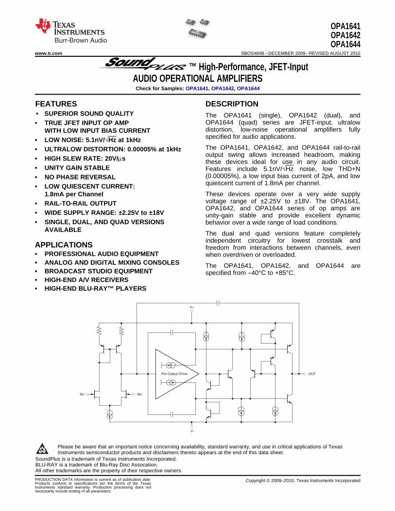
DESCRIPTION
opamp datasheet
Citation preview
OPA1642
OPA1641
OPA1644
Burr-Brown Audio
IN-
Pre-Output Driver OUT
IN+
V+
V-
OPA1641OPA1642OPA1644
www.ti.com SBOS484B –DECEMBER 2009–REVISED AUGUST 2010
™ High-Performance, JFET-InputAUDIO OPERATIONAL AMPLIFIERSCheck for Samples: OPA1641, OPA1642, OPA1644
1FEATURES DESCRIPTION234• SUPERIOR SOUND QUALITY The OPA1641 (single), OPA1642 (dual), and
OPA1644 (quad) series are JFET-input, ultralow• TRUE JFET INPUT OP AMPdistortion, low-noise operational amplifiers fullyWITH LOW INPUT BIAS CURRENTspecified for audio applications.• LOW NOISE: 5.1nV/√Hz at 1kHzThe OPA1641, OPA1642, and OPA1644 rail-to-rail• ULTRALOW DISTORTION: 0.00005% at 1kHzoutput swing allows increased headroom, making
• HIGH SLEW RATE: 20V/ms these devices ideal for use in any audio circuit.• UNITY GAIN STABLE Features include 5.1nV/√Hz noise, low THD+N
(0.00005%), a low input bias current of 2pA, and low• NO PHASE REVERSALquiescent current of 1.8mA per channel.• LOW QUIESCENT CURRENT:These devices operate over a very wide supply1.8mA per Channelvoltage range of ±2.25V to ±18V. The OPA1641,• RAIL-TO-RAIL OUTPUTOPA1642, and OPA1644 series of op amps are
• WIDE SUPPLY RANGE: ±2.25V to ±18V unity-gain stable and provide excellent dynamic• SINGLE, DUAL, AND QUAD VERSIONS behavior over a wide range of load conditions.
AVAILABLE The dual and quad versions feature completelyindependent circuitry for lowest crosstalk and
APPLICATIONS freedom from interactions between channels, even• PROFESSIONAL AUDIO EQUIPMENT when overdriven or overloaded.• ANALOG AND DIGITAL MIXING CONSOLES The OPA1641, OPA1642, and OPA1644 are• BROADCAST STUDIO EQUIPMENT specified from –40°C to +85°C. SoundPlus™• HIGH-END A/V RECEIVERS• HIGH-END BLU-RAY™ PLAYERS
1
Please be aware that an important notice concerning availability, standard warranty, and use in critical applications of TexasInstruments semiconductor products and disclaimers thereto appears at the end of this data sheet.
2SoundPlus is a trademark of Texas Instruments Incorporated.3BLU-RAY is a trademark of Blu-Ray Disc Assocation.4All other trademarks are the property of their respective owners.
PRODUCTION DATA information is current as of publication date. Copyright © 2009–2010, Texas Instruments IncorporatedProducts conform to specifications per the terms of the TexasInstruments standard warranty. Production processing does notnecessarily include testing of all parameters.
OPA1641OPA1642OPA1644SBOS484B –DECEMBER 2009–REVISED AUGUST 2010 www.ti.com
This integrated circuit can be damaged by ESD. Texas Instruments recommends that all integrated circuits be handled withappropriate precautions. Failure to observe proper handling and installation procedures can cause damage.
ESD damage can range from subtle performance degradation to complete device failure. Precision integrated circuits may be moresusceptible to damage because very small parametric changes could cause the device not to meet its published specifications.
ABSOLUTE MAXIMUM RATINGS (1)
Over operating free-air temperature range (unless otherwise noted).
VALUE UNIT
Supply Voltage, VS = (V+) – (V–) 40 V
Input Voltage (2) (V–) –0.5 to (V+) +0.5 V
Input Current (2) ±10 mA
Differential Input Voltage ±VS V
Output Short-Circuit (3) Continuous
Operating Temperature, TA –55 to +125 °C
Storage Temperature, TA –65 to +150 °C
Junction Temperature, TJ +150 °C
Human Body Model (HBM) 3000 V
ESD Ratings Charged Device Model (CDM) 1000 V
Machine Model (MM) 100 V
(1) Stresses above these ratings may cause permanent damage. Exposure to absolute maximum conditions for extended periods maydegrade device reliability. These are stress ratings only, and functional operation of the device at these or any other conditions beyondthose specified is not supported.
(2) Input terminals are diode-clamped to the power-supply rails. Input signals that can swing more than 0.5V beyond the supply rails shouldbe current-limited to 10mA or less.
(3) Short-circuit to VS/2 (ground in symmetrical dual-supply setups), one amplifier per package.
PACKAGE INFORMATION (1)
PRODUCT PACKAGE-LEAD PACKAGE DESIGNATOR PACKAGE MARKING
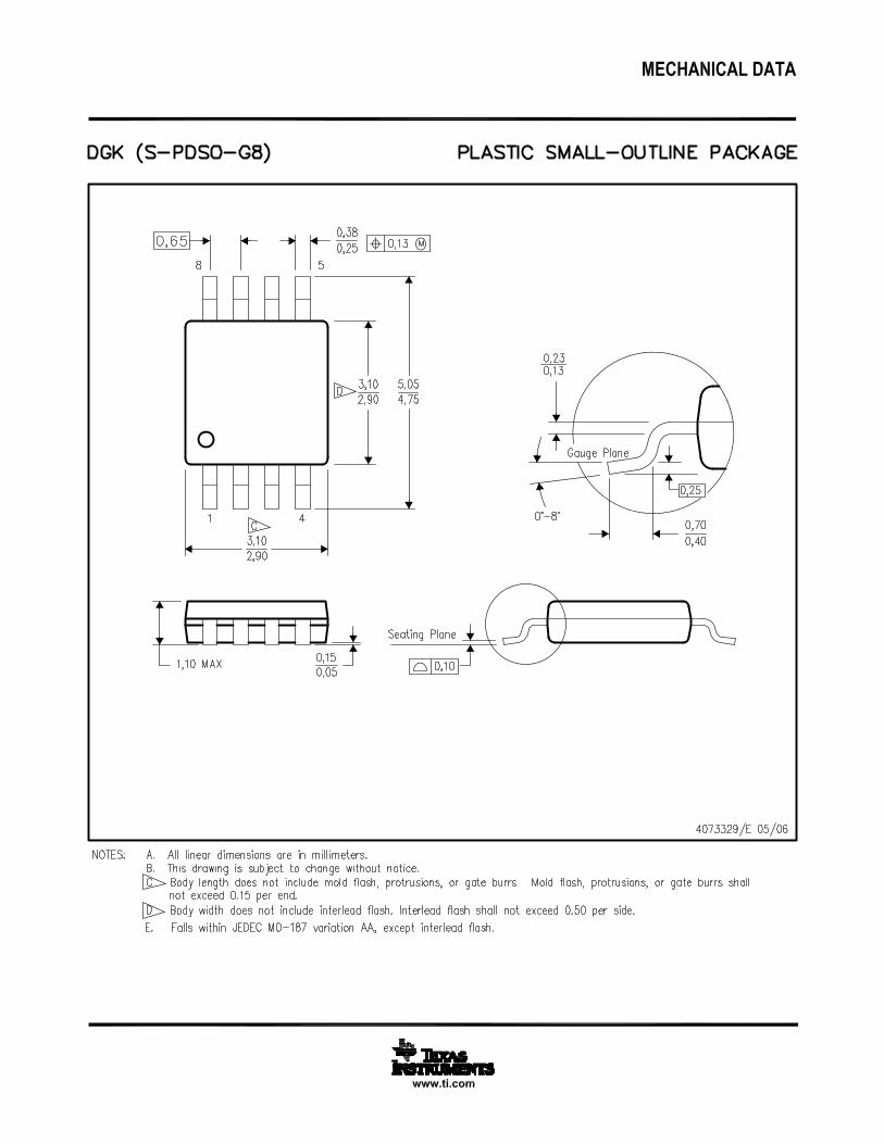
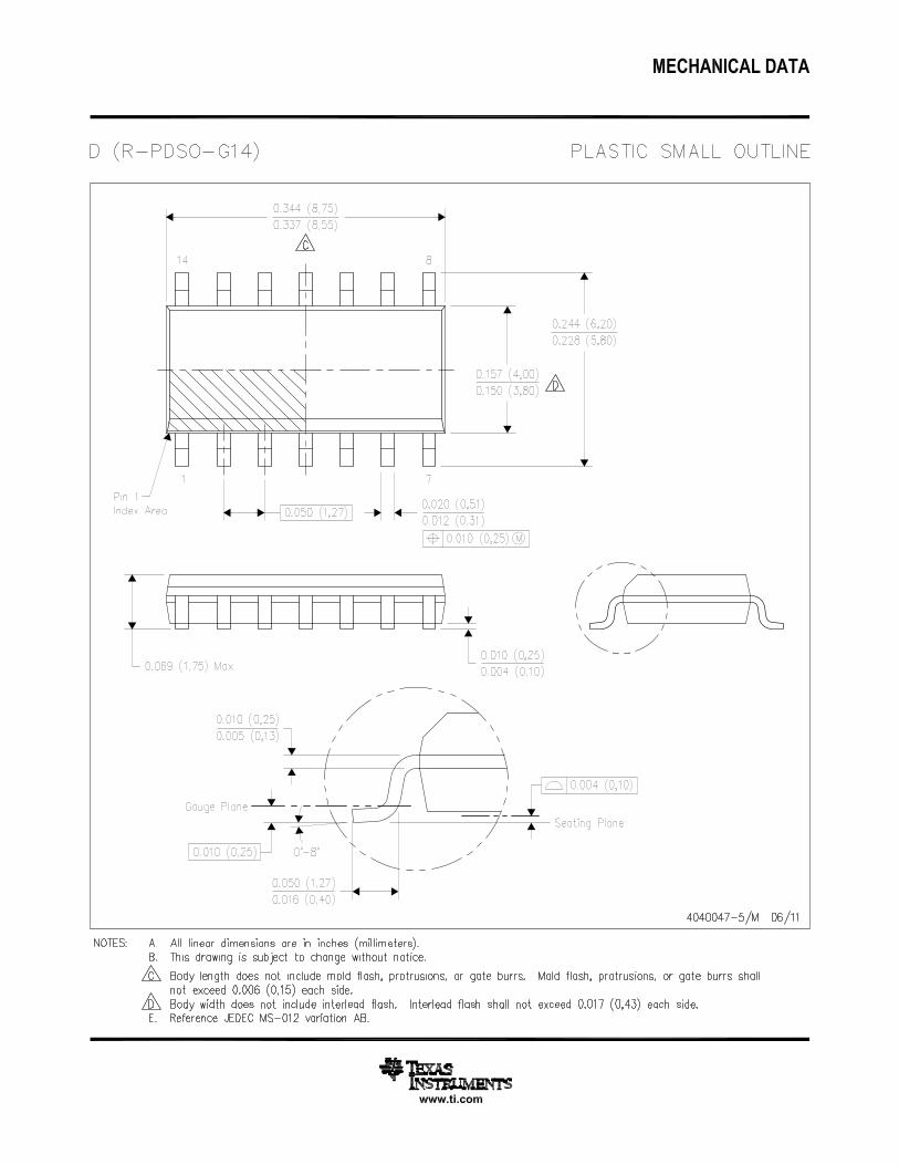
SO-8 D O1641AOPA1641
MSOP-8 DGK 1641
SO-8 D O1642AOPA1642
MSOP-8 DGK 1642
SO-14 D O1644AG4OPA1644
TSSOP-14 PW O1644A
(1) For the most current package and ordering information see the Package Option Addendum at the end of this document, or visit thedevice product folder at www.ti.com.
2 Copyright © 2009–2010, Texas Instruments Incorporated
Product Folder Link(s): OPA1641 OPA1642 OPA1644
OPA1641OPA1642OPA1644
www.ti.com SBOS484B –DECEMBER 2009–REVISED AUGUST 2010
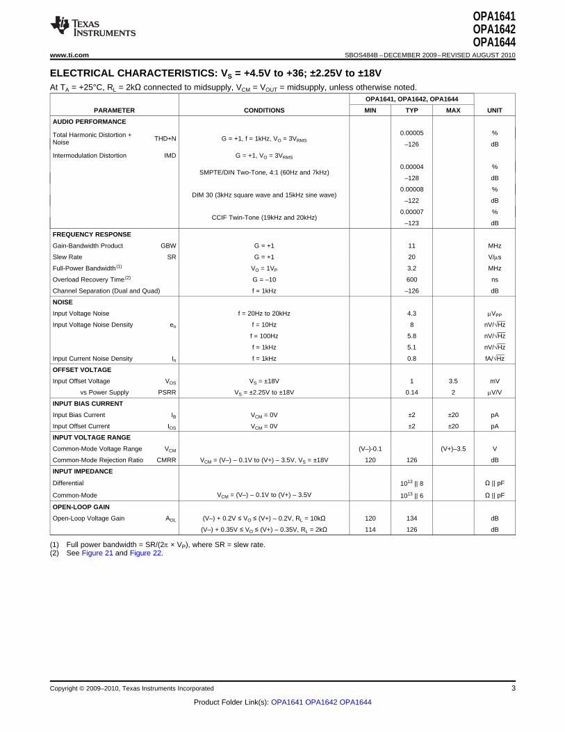
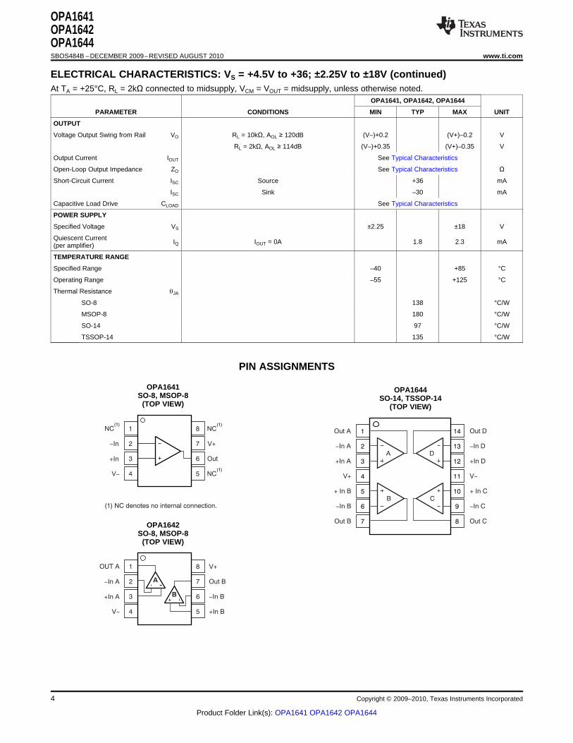
ELECTRICAL CHARACTERISTICS: VS = +4.5V to +36; ±2.25V to ±18VAt TA = +25°C, RL = 2kΩ connected to midsupply, VCM = VOUT = midsupply, unless otherwise noted.
OPA1641, OPA1642, OPA1644
PARAMETER CONDITIONS MIN TYP MAX UNIT
AUDIO PERFORMANCE
0.00005 %Total Harmonic Distortion + THD+N G = +1, f = 1kHz, VO = 3VRMSNoise –126 dB
Intermodulation Distortion IMD G = +1, VO = 3VRMS
0.00004 %SMPTE/DIN Two-Tone, 4:1 (60Hz and 7kHz)
–128 dB
0.00008 %DIM 30 (3kHz square wave and 15kHz sine wave)
–122 dB
0.00007 %CCIF Twin-Tone (19kHz and 20kHz)
–123 dB
FREQUENCY RESPONSE
Gain-Bandwidth Product GBW G = +1 11 MHz
Slew Rate SR G = +1 20 V/ms
Full-Power Bandwidth (1) VO = 1VP 3.2 MHz
Overload Recovery Time (2) G = –10 600 ns
Channel Separation (Dual and Quad) f = 1kHz –126 dB
NOISE
Input Voltage Noise f = 20Hz to 20kHz 4.3 mVPP
Input Voltage Noise Density en f = 10Hz 8 nV/√Hz
f = 100Hz 5.8 nV/√Hz
f = 1kHz 5.1 nV/√Hz
Input Current Noise Density In f = 1kHz 0.8 fA/√Hz
OFFSET VOLTAGE
Input Offset Voltage VOS VS = ±18V 1 3.5 mV
vs Power Supply PSRR VS = ±2.25V to ±18V 0.14 2 mV/V
INPUT BIAS CURRENT
Input Bias Current IB VCM = 0V ±2 ±20 pA
Input Offset Current IOS VCM = 0V ±2 ±20 pA
INPUT VOLTAGE RANGE
Common-Mode Voltage Range VCM (V–)-0.1 (V+)–3.5 V
Common-Mode Rejection Ratio CMRR VCM = (V–) – 0.1V to (V+) – 3.5V, VS = ±18V 120 126 dB
INPUT IMPEDANCE
Differential Ω || pF1013 || 8
VCM = (V–) – 0.1V to (V+) – 3.5VCommon-Mode Ω || pF1013 || 6
OPEN-LOOP GAIN
Open-Loop Voltage Gain AOL (V–) + 0.2V ≤ VO ≤ (V+) – 0.2V, RL = 10kΩ 120 134 dB
(V–) + 0.35V ≤ VO ≤ (V+) – 0.35V, RL = 2kΩ 114 126 dB
(1) Full power bandwidth = SR/(2p × VP), where SR = slew rate.(2) See Figure 21 and Figure 22.
Copyright © 2009–2010, Texas Instruments Incorporated 3
Product Folder Link(s): OPA1641 OPA1642 OPA1644
1
2
3
4
8
7
6
5
NC(1)
V+
Out
NC(1)
NC(1)
-In
+In
V-
(1) NC denotes no internal connection.
Out A
-In A
+In A
V+
+ In B
-In B
Out B
1
2
3
4
5
6
7
14
13
12
11
10
9
8
DA
B C
Out D
-In D
+In D
V-
+ In C
-In C
Out C
1
2
3
4
8
7
6
5
V+
Out B
-In B
+In B
OUT A
-In A
+In A
V-
A
B
OPA1641OPA1642OPA1644SBOS484B –DECEMBER 2009–REVISED AUGUST 2010 www.ti.com
ELECTRICAL CHARACTERISTICS: VS = +4.5V to +36; ±2.25V to ±18V (continued)At TA = +25°C, RL = 2kΩ connected to midsupply, VCM = VOUT = midsupply, unless otherwise noted.
OPA1641, OPA1642, OPA1644
PARAMETER CONDITIONS MIN TYP MAX UNIT
OUTPUT
Voltage Output Swing from Rail VO RL = 10kΩ, AOL ≥ 120dB (V–)+0.2 (V+)–0.2 V
RL = 2kΩ, AOL ≥ 114dB (V–)+0.35 (V+)–0.35 V
Output Current IOUT See Typical Characteristics
Open-Loop Output Impedance ZO See Typical Characteristics Ω
Short-Circuit Current ISC Source +36 mA
ISC Sink –30 mA
Capacitive Load Drive CLOAD See Typical Characteristics
POWER SUPPLY
Specified Voltage VS ±2.25 ±18 V
Quiescent Current IQ IOUT = 0A 1.8 2.3 mA(per amplifier)
TEMPERATURE RANGE
Specified Range –40 +85 °C
Operating Range –55 +125 °C
Thermal Resistance qJA
SO-8 138 °C/W
MSOP-8 180 °C/W
SO-14 97 °C/W
TSSOP-14 135 °C/W
PIN ASSIGNMENTS
OPA1641 OPA1644SO-8, MSOP-8 SO-14, TSSOP-14
(TOP VIEW) (TOP VIEW)
OPA1642SO-8, MSOP-8
(TOP VIEW)
4 Copyright © 2009–2010, Texas Instruments Incorporated
Product Folder Link(s): OPA1641 OPA1642 OPA1644
100nV
/div
Time (1s/div)
Voltage N
ois
e D
ensity (
nV
/)
ÖH
z
0.1
Frequency (Hz)
100k101 100 1k 10k
100
10
1
160
140
120
100
80
60
40
20
0
Com
mon-M
ode R
eje
ction R
atio (
dB
)
Pow
er-
Supply
Reje
ction R
atio (
dB
)
1 10 100 1k 10k 100k 1M 10M 100M
Frequency (Hz)
CMRR
+PSRR
-PSRR
35
30
25
20
15
10
5
0
Outp
ut V
oltage (
V)
PP
10k 100k 1M 10M
Frequency (Hz)
V = 2.25VS ±
V = 5VS ±
V = 15VS ±
Maximum output
voltage range
without slew-rate
induced distortion
140
120
100
80
60
40
20
0
20-
180
135
90
45
0
Ga
in (
dB
)
Ph
ase
(de
gre
es)
50 100 1k 10k 100k 1M 10M 100M
Frequency (Hz)
Phase
Gain
30
20
10
0
10
20
-
-
Gain
(dB
)
100k 1M 10M 100M
Frequency (Hz)
G = +10
G = +1
G = 1-
OPA1641OPA1642OPA1644
www.ti.com SBOS484B –DECEMBER 2009–REVISED AUGUST 2010
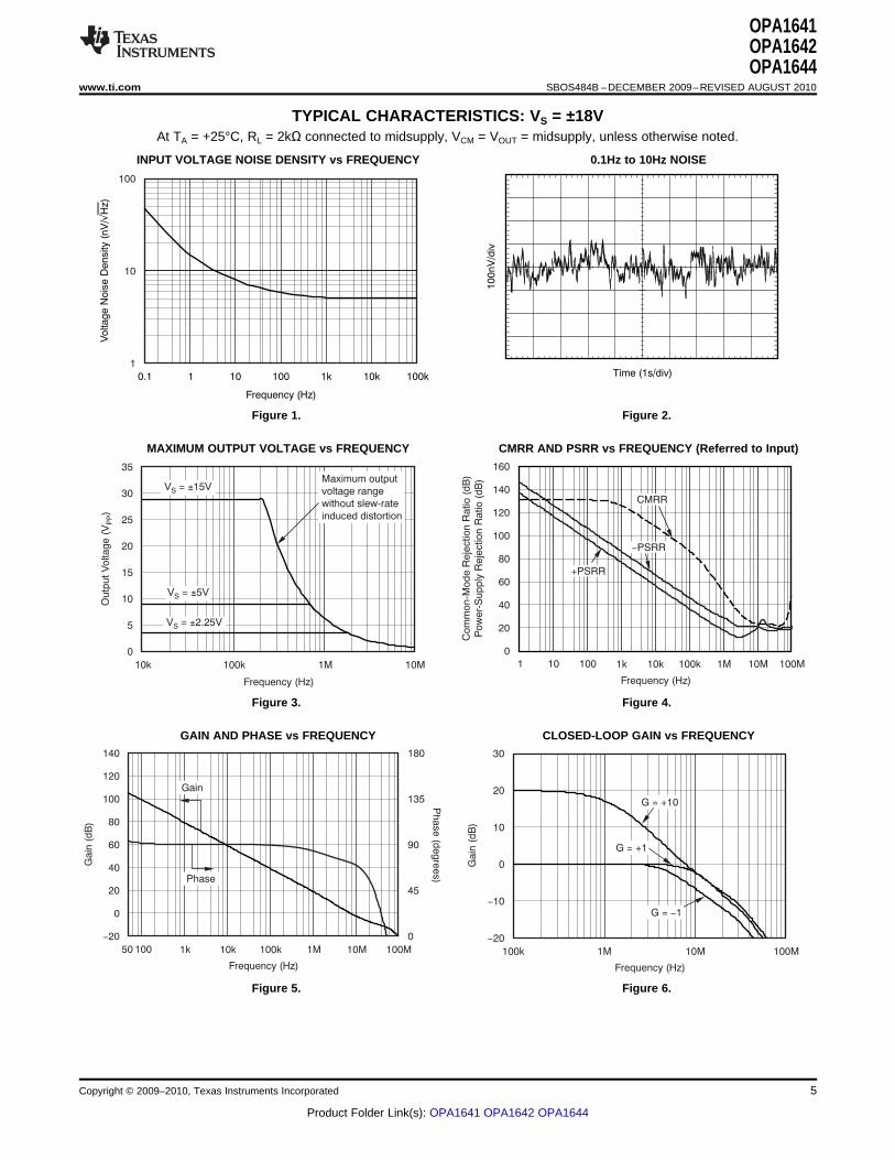
TYPICAL CHARACTERISTICS: VS = ±18VAt TA = +25°C, RL = 2kΩ connected to midsupply, VCM = VOUT = midsupply, unless otherwise noted.
INPUT VOLTAGE NOISE DENSITY vs FREQUENCY 0.1Hz to 10Hz NOISE
Figure 1. Figure 2.
MAXIMUM OUTPUT VOLTAGE vs FREQUENCY CMRR AND PSRR vs FREQUENCY (Referred to Input)
Figure 3. Figure 4.
GAIN AND PHASE vs FREQUENCY CLOSED-LOOP GAIN vs FREQUENCY
Figure 5. Figure 6.
Copyright © 2009–2010, Texas Instruments Incorporated 5
Product Folder Link(s): OPA1641 OPA1642 OPA1644
0.01
0.001
0.0001
0.00001
-
-
-
-
80
100
120
140
Tota
l Ha
rmo
nic
Dis
tortio
n +
No
ise
(dB
)Tota
l H
arm
on
ic D
isto
rtio
n +
No
ise
(%
)
10 100 1k 10k 20k
Frequency (Hz)
R = 600WSOURCE
R = 300WSOURCE
R
= 150SOURCE
W
V = 3V
BW = 80kHzOUT RMS
OPA1641
+15V
-15V RL
RSOURCE
R = 0WSOURCE
0.001
0.0001
0.00001
-100
-
-
120
140
Tota
l H
arm
onic
Dis
tort
ion +
Nois
e (
%) To
tal H
arm
onic
Dis
tortio
n +
Nois
e (d
B)
10 100 1k 10k 20k
Frequency (Hz)
G = +1
R = 600L W
G = +1
R = 2kL W
G = -1
R = 2kL W
V = 3V
BW = 80kHzOUT RMS
G = 1
R = 600
-
WL
0.01
0.001
0.0001
0.00001
Tota
l H
arm
onic
Dis
tort
ion +
Nois
e (
%)
10 100 1k 10k 100k
Frequency (Hz)
G = 1
R = 2k
-
WL
G = 1
R = 600
-
WL
V = 3V
BW > 500kHzOUT RMS
G = +1
R = 2kL W
G = +1
R = 600L W
-
-
-
-
80
100
120
140
Tota
l Harm
onic
Dis
tortio
n +
Nois
e (d
B)
0.01
0.001
0.0001
0.00001
Tota
l H
arm
onic
Dis
tort
ion +
Nois
e (
%)
10 100 1k 10k 100k
Frequency (Hz)
V = 3V
BW > 500kHzOUT RMS
R = 0WSOURCE
R = 300WSOURCE
R
= 150SOURCE
W
R = 600WSOURCE
OPA1641
+15V
-15V RL
RSOURCE
-
-
-
-
80
100
120
140
Tota
l Harm
onic
Dis
tortio
n +
Nois
e (d
B)
0.01
0.001
0.0001
0.00001
Tota
l H
arm
onic
Dis
tort
ion +
Nois
e (
%) To
tal H
arm
onic
Dis
tortio
n +
Nois
e (d
B)
0.1 1 10 20
Output Amplitude (V )RMS
-
-
-
80
100
120
140-
BW = 80kHz
R = 0SOURCE W
1kHz Signal
G = 1,- R = 2k
R = 2kL
L
W
WG = +1,
0.01
0.001
0.0001
0.00001
Inte
rmodula
tion D
isto
rtio
n (
%) In
term
odula
tion D
isto
rtion (d
B)
0.1 1 10 20
Output Amplitude (V )RMS
-
-
-
80
100
120
140-
G = +1
SMPTE/DIN
Two-Tone
4:1 (60Hz and 7kHz)
CCIF Twin-Tone
(19kHz and 20kHz)
DIM30
(3kHz square wave
and 15kHz sine wave)
OPA1641OPA1642OPA1644SBOS484B –DECEMBER 2009–REVISED AUGUST 2010 www.ti.com
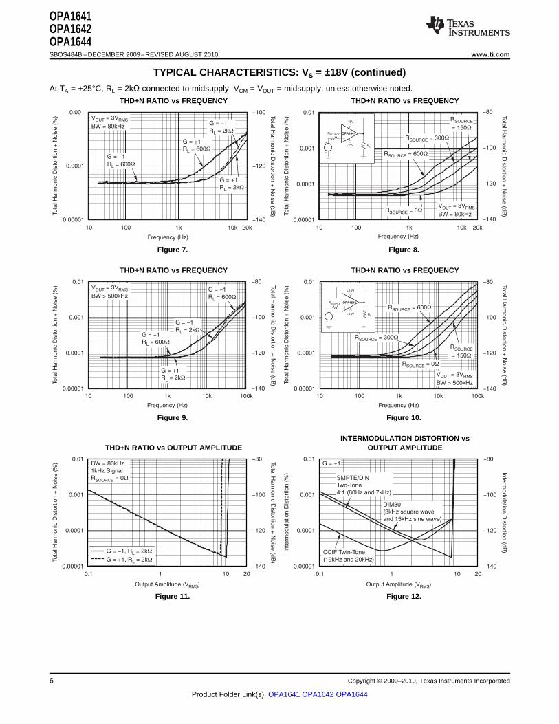
TYPICAL CHARACTERISTICS: VS = ±18V (continued)
At TA = +25°C, RL = 2kΩ connected to midsupply, VCM = VOUT = midsupply, unless otherwise noted.
THD+N RATIO vs FREQUENCY THD+N RATIO vs FREQUENCY
Figure 7. Figure 8.
THD+N RATIO vs FREQUENCY THD+N RATIO vs FREQUENCY
Figure 9. Figure 10.
INTERMODULATION DISTORTION vsTHD+N RATIO vs OUTPUT AMPLITUDE OUTPUT AMPLITUDE
Figure 11. Figure 12.
6 Copyright © 2009–2010, Texas Instruments Incorporated
Product Folder Link(s): OPA1641 OPA1642 OPA1644
Output
Output
Time (0.4 s/div)m
5V
/div
+18V
-18V
37VPP
Sine Wave
( 18.5V)±
OPA1641
-
-
-
-
-
-
-
80
90
100
110
120
130
140
Channel S
epara
tion (
dB
)
10
Frequency (Hz)
100k100 1k 10k
V = 15VS
V = 3VOUT RMS
G = +1
±
R = 2kWL
R = 600WL
LR = 5kW
Time (100ns/div)
20m
V/d
ivG = 1
C = 100pF
-
L
+15V
-15V
R 2kWF =R 2kWI =
CL
OPA1641
20m
V/d
iv
Time (100ns/div)
G = +1
C = 100pFL
+15V
-15V CLRL
OPA1641
2V
/div
Time (400ns/div)
G = +1
C = 100pFL
2V
/div
Time (400ns/div)
G = 1
C = 100pF
-
L
OPA1641OPA1642OPA1644
www.ti.com SBOS484B –DECEMBER 2009–REVISED AUGUST 2010
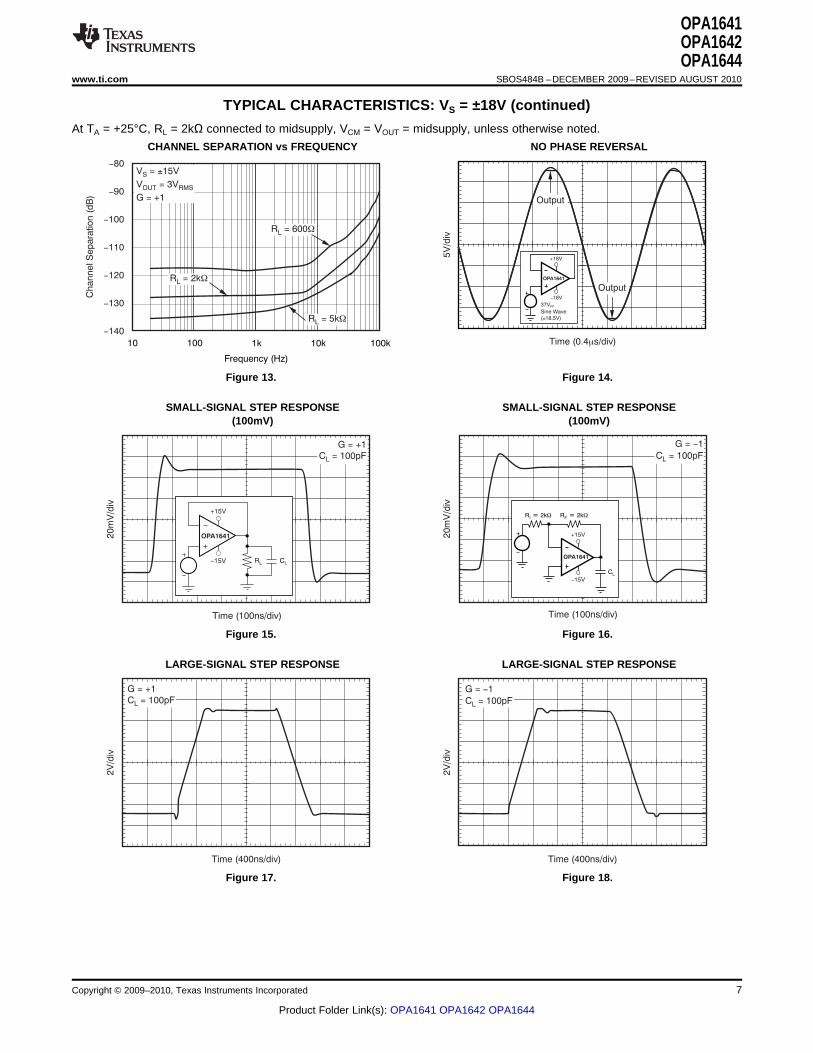
TYPICAL CHARACTERISTICS: VS = ±18V (continued)
At TA = +25°C, RL = 2kΩ connected to midsupply, VCM = VOUT = midsupply, unless otherwise noted.
CHANNEL SEPARATION vs FREQUENCY NO PHASE REVERSAL
Figure 13. Figure 14.
SMALL-SIGNAL STEP RESPONSE SMALL-SIGNAL STEP RESPONSE(100mV) (100mV)
Figure 15. Figure 16.
LARGE-SIGNAL STEP RESPONSE LARGE-SIGNAL STEP RESPONSE
Figure 17. Figure 18.
Copyright © 2009–2010, Texas Instruments Incorporated 7
Product Folder Link(s): OPA1641 OPA1642 OPA1644
Time (0.4 s/div)m
2kW
20kW
VIN
VOUTOPA1641
5V
/div
VIN
VOUT G = 10-
Time (0.4 s/div)m
2kW
20kW
VIN
VOUTOPA1641
5V
/div
VIN
VOUT
G = 10-
40
35
30
25
20
15
10
5
0
Overs
hoot (%
)
0 100 200 300 400 500 600 700 800 900 1000
Capacitive Load (pF)
R = 0WOUT
R = 24WOUT
R = 51WOUT
+15V
-15V
ROUT
CL
OPA1641
RL
G = +145
40
35
30
25
20
15
10
5
0
Overs
hoot (%
)
0 100 200 300 400 500 600 700 800 900 1000
Capacitive Load (pF)
R = 0WOUT
R = 24WOUT
R = 51WOUT
OPA1641
R =I 2kW
ROUT
CL
RF = 2kW
+15V
-15V
G = 1-
80
70
60
50
40
30
20
10
0
10
20
-
-
Iand I
(pA
)B
OS
-40 -15 10 35 60 85
Temperature ( C)°
-IB
+IB
-IOS
0
0.2
0.4
0.6
0.8
1.0
1.2
-
-
-
-
-
-
A(
V/V
)m
OL
-40 -15 10 35 60 85
Temperature ( C)°
10kW
2kW
OPA1641OPA1642OPA1644SBOS484B –DECEMBER 2009–REVISED AUGUST 2010 www.ti.com
TYPICAL CHARACTERISTICS: VS = ±18V (continued)
At TA = +25°C, RL = 2kΩ connected to midsupply, VCM = VOUT = midsupply, unless otherwise noted.
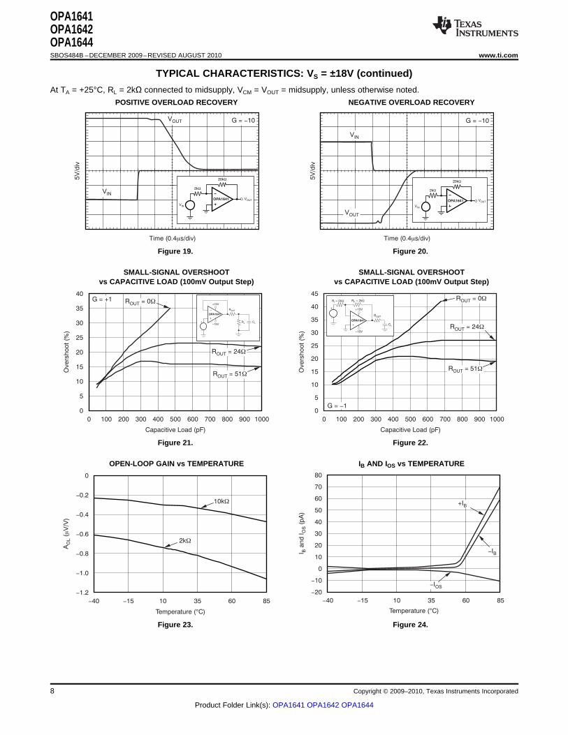
POSITIVE OVERLOAD RECOVERY NEGATIVE OVERLOAD RECOVERY
Figure 19. Figure 20.
SMALL-SIGNAL OVERSHOOT SMALL-SIGNAL OVERSHOOTvs CAPACITIVE LOAD (100mV Output Step) vs CAPACITIVE LOAD (100mV Output Step)
Figure 21. Figure 22.
OPEN-LOOP GAIN vs TEMPERATURE IB AND IOS vs TEMPERATURE
Figure 23. Figure 24.
8 Copyright © 2009–2010, Texas Instruments Incorporated
Product Folder Link(s): OPA1641 OPA1642 OPA1644
10
8
6
4
2
0
2
4
6
8
10
-
-
-
-
-
Iand I
(pA
)B
OS
-18 -12 -6 0 6 12 18
Common-Mode Voltage (V)
V = 18VS ±
+IB
IOS
-IB
Common-Mode Range
2.5
2.0
1.5
1.0
0.5
0
I(m
A)
Q
-40 -10 20 50 655 35 80 95 110 125
Temperature ( C)°
-25
60
50
40
30
20
10
0
I SC
(mA
)
-50 -25 0 25 50 75 100 125
Temperature ( C)°
ISC-SINK
ISC-SOURCE
V = Midsupply
(includes self-heating)OUT
2.00
1.75
1.50
1.25
1.00
0.75
0.50
0.25
0
I(m
A)
Q
0 4 8 12 16 20 24 28 32 36
Supply Voltage (V)
Specified Supply-Voltage Range
Outp
ut V
oltage (
V)
0 10 20 30 40 50
Output Current (mA)
+85 C°
+25 C°-40 C°
18.0
17.5
17.0
16.5
16.0
-16.0
16.5
17.0
17.5
18.0
-
-
-
-
+125 C°
Z(
)W
O
10
Frequency (Hz)
100M100 1k 10k 100k 10M1M
1k
100
10
1
OPA1641OPA1642OPA1644
www.ti.com SBOS484B –DECEMBER 2009–REVISED AUGUST 2010
TYPICAL CHARACTERISTICS: VS = ±18V (continued)
At TA = +25°C, RL = 2kΩ connected to midsupply, VCM = VOUT = midsupply, unless otherwise noted.
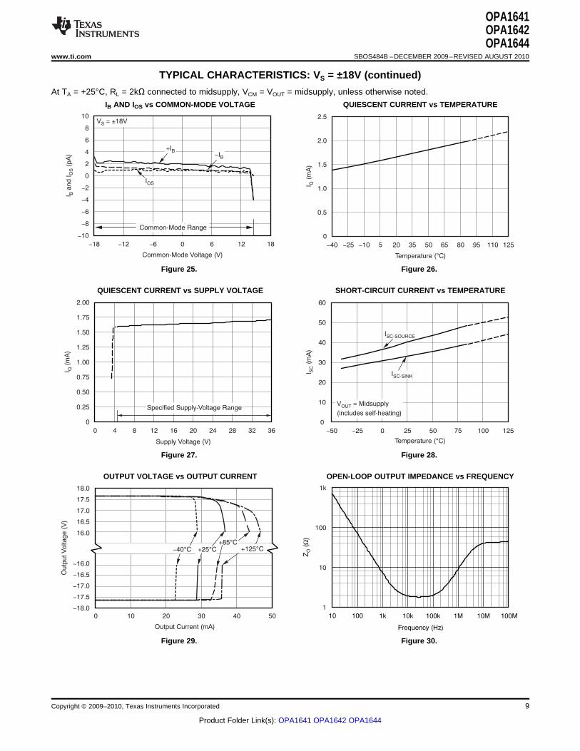
IB AND IOS vs COMMON-MODE VOLTAGE QUIESCENT CURRENT vs TEMPERATURE
Figure 25. Figure 26.
QUIESCENT CURRENT vs SUPPLY VOLTAGE SHORT-CIRCUIT CURRENT vs TEMPERATURE
Figure 27. Figure 28.
OUTPUT VOLTAGE vs OUTPUT CURRENT OPEN-LOOP OUTPUT IMPEDANCE vs FREQUENCY
Figure 29. Figure 30.
Copyright © 2009–2010, Texas Instruments Incorporated 9
Product Folder Link(s): OPA1641 OPA1642 OPA1644
100k 1M
Source Resistance, R (W)S
100 1k 10k
10k
1k
100
10
1
Votlage N
ois
e S
pectr
al D
ensity,
EO
RS
EO
E = eO n n S S+ (i R ) + 4kTR2 2 2
Resistor Noise
OPA1611
OPA1641
OPA1641OPA1642OPA1644SBOS484B –DECEMBER 2009–REVISED AUGUST 2010 www.ti.com
APPLICATION INFORMATION
The OPA1641, OPA1642, and OPA1644 are The equation in Figure 31 shows the calculation ofunity-gain stable, audio operational amplifiers with the total circuit noise, with these parameters:very low noise, input bias current, and input offset • en = voltage noisevoltage. Applications with noisy or high-impedance • In = current noisepower supplies require decoupling capacitors placed
• RS = source impedanceclose to the device pins. In most cases, 0.1mF• k = Boltzmann's constant = 1.38 × 10⁻²³ J/Kcapacitors are adequate. The front-page drawing
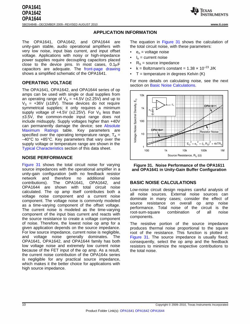
shows a simplified schematic of the OPA1641. • T = temperature in degrees Kelvin (K)
For more details on calculating noise, see the nextOPERATING VOLTAGEsection on Basic Noise Calculations.
The OPA1641, OPA1642, and OPA1644 series of opamps can be used with single or dual supplies froman operating range of VS = +4.5V (±2.25V) and up toVS = +36V (±18V). These devices do not requiresymmetrical supplies; it only requires a minimumsupply voltage of +4.5V (±2.25V). For VS less than±3.5V, the common-mode input range does notinclude midsupply. Supply voltages higher than +40Vcan permanently damage the device; see AbsoluteMaximum Ratings table. Key parameters arespecified over the operating temperature range, TA =–40°C to +85°C. Key parameters that vary over thesupply voltage or temperature range are shown in theTypical Characteristics section of this data sheet.
NOISE PERFORMANCE
Figure 31 shows the total circuit noise for varying Figure 31. Noise Performance of the OPA1611source impedances with the operational amplifier in a and OPA1641 in Unity-Gain Buffer Configurationunity-gain configuration (with no feedback resistornetwork and therefore no additional noisecontributions). The OPA1641, OPA1642, and BASIC NOISE CALCULATIONSOPA1644 are shown with total circuit noise
Low-noise circuit design requires careful analysis ofcalculated. The op amp itself contributes both aall noise sources. External noise sources canvoltage noise component and a current noisedominate in many cases; consider the effect ofcomponent. The voltage noise is commonly modeledsource resistance on overall op amp noiseas a time-varying component of the offset voltage.performance. Total noise of the circuit is theThe current noise is modeled as the time-varyingroot-sum-square combination of all noisecomponent of the input bias current and reacts withcomponents.the source resistance to create a voltage component
of noise. Therefore, the lowest noise op amp for a The resistive portion of the source impedancegiven application depends on the source impedance. produces thermal noise proportional to the squareFor low source impedance, current noise is negligible, root of the resistance. This function is plotted inand voltage noise generally dominates. The Figure 31. The source impedance is usually fixed;OPA1641, OPA1642, and OPA1644 family has both consequently, select the op amp and the feedbacklow voltage noise and extremely low current noise resistors to minimize the respective contributions tobecause of the FET input of the op amp. As a result, the total noise.the current noise contribution of the OPA164x seriesis negligible for any practical source impedance,which makes it the better choice for applications withhigh source impedance.
10 Copyright © 2009–2010, Texas Instruments Incorporated
Product Folder Link(s): OPA1641 OPA1642 OPA1644
R1
R2
EO
R1
R2
EORS
VS
RS
VS
A) Noise in Noninverting Gain Configuration
B) Noise in Inverting Gain Configuration
Noise at the output:
Where e =S4kTRS
4kTR1
4kTR2
= thermal noise of RS
= thermal noise of R1
= thermal noise of R2
e =1
e =2
Noise at the output:
E =O
21 +
R2
R + R1 S
R2
R + R1 S
2 22
Where e =S4kTRS
4kTR1
4kTR2
= thermal noise of RS
= thermal noise of R1
= thermal noise of R2
e =1
e =2
R2
R + R1 S
2
1 +R2
R1
1 +R2
R1
2
R2
R1
2
e + e +1 2
2 2E =O
2e +n
2es
2
For the OPA164x series op amps at 1kHz, e = 5.1nV/ Hzn Ö
e + e +1 2
2 2es
2e +n
2
OPA1641OPA1642OPA1644
www.ti.com SBOS484B –DECEMBER 2009–REVISED AUGUST 2010
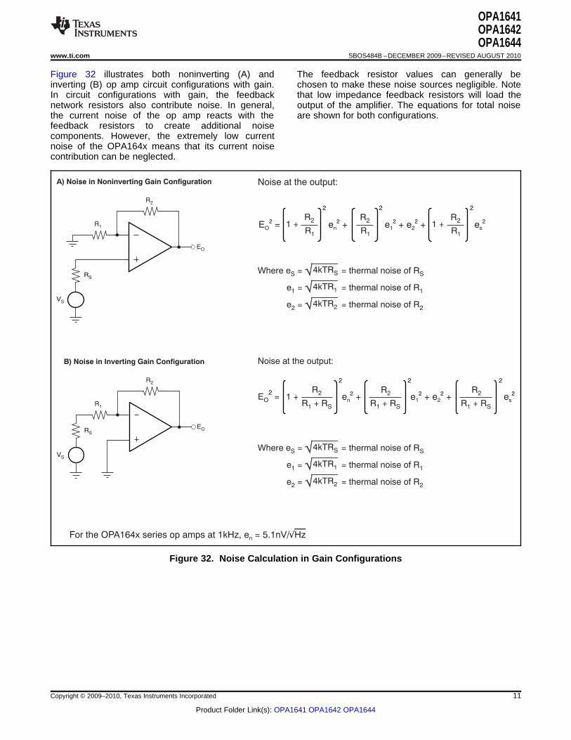
Figure 32 illustrates both noninverting (A) and The feedback resistor values can generally beinverting (B) op amp circuit configurations with gain. chosen to make these noise sources negligible. NoteIn circuit configurations with gain, the feedback that low impedance feedback resistors will load thenetwork resistors also contribute noise. In general, output of the amplifier. The equations for total noisethe current noise of the op amp reacts with the are shown for both configurations.feedback resistors to create additional noise
spacecomponents. However, the extremely low currentnoise of the OPA164x means that its current noise spacecontribution can be neglected.
Figure 32. Noise Calculation in Gain Configurations
Copyright © 2009–2010, Texas Instruments Incorporated 11
Product Folder Link(s): OPA1641 OPA1642 OPA1644
R2
OPA1641
R1
Signal Gain = 1+
Distortion Gain = 1+
R3 V = 3VO RMS
Generator
Output
Analyzer
Input
Audio Precision
System Two(1)
with PC Controller
SIGNAL
GAIN
DISTORTION
GAIN R1
R2
R3
¥
100W
1kW
1kW
10W
11W
1
11
101
101R2
R1
R2
R II R1 3
Load
OPA1641OPA1642OPA1644SBOS484B –DECEMBER 2009–REVISED AUGUST 2010 www.ti.com
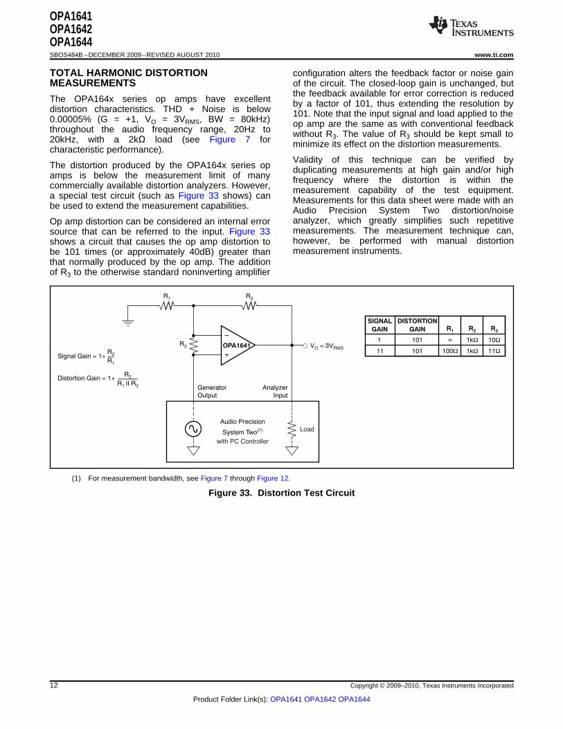
TOTAL HARMONIC DISTORTION configuration alters the feedback factor or noise gainMEASUREMENTS of the circuit. The closed-loop gain is unchanged, but
the feedback available for error correction is reducedThe OPA164x series op amps have excellent by a factor of 101, thus extending the resolution bydistortion characteristics. THD + Noise is below 101. Note that the input signal and load applied to the0.00005% (G = +1, VO = 3VRMS, BW = 80kHz) op amp are the same as with conventional feedbackthroughout the audio frequency range, 20Hz to without R3. The value of R3 should be kept small to20kHz, with a 2kΩ load (see Figure 7 for minimize its effect on the distortion measurements.characteristic performance).
Validity of this technique can be verified byThe distortion produced by the OPA164x series op duplicating measurements at high gain and/or highamps is below the measurement limit of many frequency where the distortion is within thecommercially available distortion analyzers. However, measurement capability of the test equipment.a special test circuit (such as Figure 33 shows) can Measurements for this data sheet were made with anbe used to extend the measurement capabilities. Audio Precision System Two distortion/noise
analyzer, which greatly simplifies such repetitiveOp amp distortion can be considered an internal errormeasurements. The measurement technique can,source that can be referred to the input. Figure 33however, be performed with manual distortionshows a circuit that causes the op amp distortion tomeasurement instruments.be 101 times (or approximately 40dB) greater than
that normally produced by the op amp. The addition spaceof R3 to the otherwise standard noninverting amplifier
(1) For measurement bandwidth, see Figure 7 through Figure 12.
Figure 33. Distortion Test Circuit
12 Copyright © 2009–2010, Texas Instruments Incorporated
Product Folder Link(s): OPA1641 OPA1642 OPA1644
OPA164x
If R > 2k or R || R > 2k
R = R || R
W WS 1 2
S 1 2
VIN
VOUT
R1R1 R2
OPA1641OPA1642OPA1644
www.ti.com SBOS484B –DECEMBER 2009–REVISED AUGUST 2010
SOURCE IMPEDANCE AND DISTORTION PHASE-REVERSAL PROTECTION
For lowest distortion with a source or feedback The OPA1641, OPA1642, and OPA1644 family hasnetwork, the impedance seen by the positive and internal phase-reversal protection. Many FET- andnegative inputs in noninverting applications should be bipolar-input op amps exhibit a phase reversal whenmatched. The n-channel JFETs in the FET input the input is driven beyond its linear common-modestage exhibit a varying input capacitance with applied range. This condition is most often encountered incommon-mode input voltage. In inverting noninverting circuits when the input is driven beyondconfigurations, the input does not vary with input the specified common-mode voltage range, causingvoltage because the inverting input is held at virtual the output to reverse into the opposite rail. The inputground. However, in noninverting applications, the circuitry of the OPA1641, OPA1642, and OPA1644inputs do vary, and the gate-to-source voltage is not prevents phase reversal with excessiveconstant. This effect produces increased distortion as common-mode voltage; instead, the output limits intoa result of the varying capacitance for unmatched the appropriate rail (see Figure 14).source impedances.
OUTPUT CURRENT LIMITTo maintain low distortion, match unbalanced sourceimpedance with appropriate values in the feedback The output current of the OPA164x series is limitednetwork as shown in Figure 34. Of course, the by internal circuitry to +36mA/–30mAunbalanced impedance may be from gain-setting (sourcing/sinking), to protect the device if the outputresistors in the feedback path. If the parallel is accidentally shorted. This short-circuit currentcombination of R1 and R2 is greater than 2kΩ, a depends on temperature, as shown in Figure 28.matching impedance on the noninverting input should
Although it is uncommon for most modern audiobe used. As always, resistor values should beapplications to require 600Ω load drive capability,minimized to reduce the effects of thermal noise.many audio op amp applications continue to specifythe total harmonic distortion (THD+N) at 600Ω loadfor comparative purposes. Figure 7 and Figure 9provide typical THD+N measurement curves for theOPA164x series, where the output drives a 3VRMSsignal into a 600Ω load. However, it should be notedthat correct device operation cannot be ensured whendriving 600Ω loads at full supply. Depending onsupply voltage and temperature, it may well triggerthe output current limit circuitry of the device.
POWER DISSIPATION AND THERMALFigure 34. Impedance Matching for Maintaining PROTECTION
Low Distortion in Noninverting CircuitsThe OPA164x series of op amps are capable ofdriving 2kΩ loads with power-supply voltages of up to±18V over the specified temperature range. In aCAPACITIVE LOAD AND STABILITYsingle-supply configuration, where the load is
The dynamic characteristics of the OPA164x have connected to the negative supply voltage, thebeen optimized for commonly encountered gains, minimum load resistance is 2.8kΩ at a supply voltageloads, and operating conditions. The combination of of +36V. For lower supply voltages (eitherlow closed-loop gain and high capacitive loads single-supply or symmetrical supplies), a lower loaddecreases the phase margin of the amplifier and can resistance may be used, as long as the output currentlead to gain peaking or oscillations. As a result, does not exceed 13mA; otherwise, the deviceheavier capacitive loads must be isolated from the short-circuit current protection circuit may activate.output. The simplest way to achieve this isolation is to
Internal power dissipation increases when operatingadd a small resistor (ROUT equal to 50Ω, for example)at high supply voltages. Copper leadframein series with the output.construction used in the OPA1641, OPA1642, and
Figure 21 and Figure 22 illustrate graphs of OPA1644 series devices improves heat dissipationSmall-Signal Overshoot vs Capacitive Load for compared to conventional materials. PCB layout canseveral values of ROUT. Also, refer to Applications also help reduce a possible increase in junctionBulletin AB-028 (literature number SBOA015, temperature. Wide copper traces help dissipate theavailable for download from the TI web site) for heat by acting as an additional heatsink. Temperaturedetails of analysis techniques and application circuits. rise can be further minimized by soldering the
devices directly to the PCB rather than using asocket.
Copyright © 2009–2010, Texas Instruments Incorporated 13
Product Folder Link(s): OPA1641 OPA1642 OPA1644
OPA1641OPA1642OPA1644SBOS484B –DECEMBER 2009–REVISED AUGUST 2010 www.ti.com
Although the output current is limited by internal An ESD event produces a short duration,protection circuitry, accidental shorting of one or more high-voltage pulse that is transformed into a shortoutput channels of a device can result in excessive duration, high-current pulse as it discharges throughheating. For instance, when an output is shorted to a semiconductor device. The ESD protection circuitsmid-supply, the typical short-circuit current of 36mA are designed to provide a current path around theleads to an internal power dissipation of over 600mW operational amplifier core to prevent it from beingat a supply of ±18V. In case of a dual OPA1642 in an damaged. The energy absorbed by the protectionMSOP-8 package (thermal resistance qJA = circuitry is then dissipated as heat.180°C/W), such a power dissipation would lead the
When an ESD voltage develops across two or moredie temperature to be 220°C above ambientof the amplifier device pins, current flows through onetemperature, when both channels are shorted. Thisor more of the steering diodes. Depending on thetemperature increase would destroy the device.path that the current takes, the absorption device
In order to prevent such excessive heating that can may activate. The absorption device has a trigger, ordestroy the device, the OPA164x series has an threshold voltage, that is above the normal operatinginternal thermal shutdown circuit, which shuts down voltage of the OPA164x but below the devicethe device if the die temperature exceeds breakdown voltage level. Once this threshold isapproximately +180°C. Once this thermal shutdown exceeded, the absorption device quickly activatescircuit activates, a built-in hysteresis of 15°C ensures and clamps the voltage across the supply rails to athat the die temperature must drop to about +165°C safe level.before the device switches on again.
When the operational amplifier connects into a circuitsuch as the one Figure 35 shows, the ESD protectionELECTRICAL OVERSTRESS components are intended to remain inactive and notbecome involved in the application circuit operation.Designers often ask questions about the capability ofHowever, circumstances may arise where an appliedan operational amplifier to withstand electricalvoltage exceeds the operating voltage range of aoverstress. These questions tend to focus on thegiven pin. Should this condition occur, there is a riskdevice inputs, but may involve the supply voltage pinsthat some of the internal ESD protection circuits mayor even the output pin. Each of these different pinbe biased on, and conduct current. Any such currentfunctions have electrical stress limits determined byflow occurs through steering diode paths and rarelythe voltage breakdown characteristics of theinvolves the absorption device.particular semiconductor fabrication process and
specific circuits connected to the pin. Additionally, Figure 35 depicts a specific example where the inputinternal electrostatic discharge (ESD) protection is voltage, VIN, exceeds the positive supply voltagebuilt into these circuits to protect them from (+VS) by 500mV or more. Much of what happens inaccidental ESD events both before and during the circuit depends on the supply characteristics. Ifproduct assembly. +VS can sink the current, one of the upper input
steering diodes conducts and directs current to +VS.It is helpful to have a good understanding of thisExcessively high current levels can flow withbasic ESD circuitry and its relevance to an electricalincreasingly higher VIN. As a result, the datasheetoverstress event. Figure 35 illustrates the ESDspecifications recommend that applications limit thecircuits contained in the OPA164x series (indicatedinput current to 10mA.by the dashed line area). The ESD protection circuitry
involves several current-steering diodes connected If the supply is not capable of sinking the current, VINfrom the input and output pins and routed back to the may begin sourcing current to the operationalinternal power-supply lines, where they meet at an amplifier, and then take over as the source of positiveabsorption device internal to the operational amplifier. supply voltage. The danger in this case is that theThis protection circuitry is intended to remain inactive voltage can rise to levels that exceed the operationalduring normal circuit operation. amplifier absolute maximum ratings.
14 Copyright © 2009–2010, Texas Instruments Incorporated
Product Folder Link(s): OPA1641 OPA1642 OPA1644
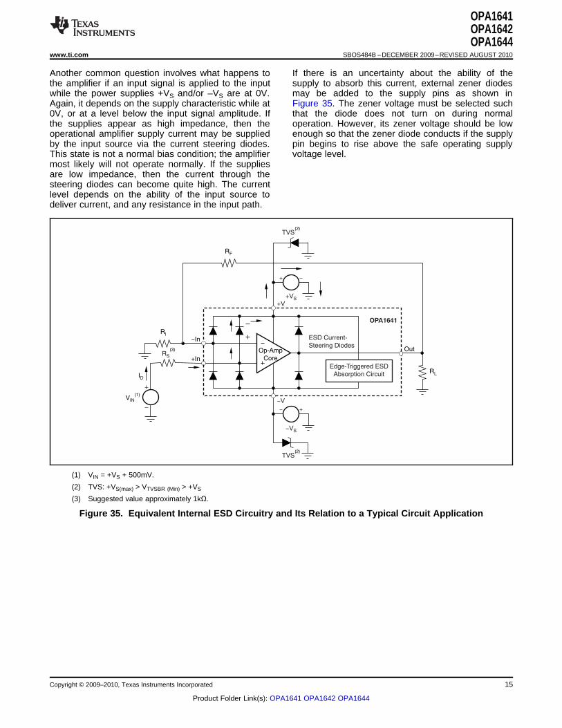
RF
Op-Amp
Core
RI
RL
V(1)
IN
ID
-In
Out
+In
ESD Current-
Steering Diodes
Edge-Triggered ESD
Absorption Circuit
+VS
+V
-V
-VS
OPA1641
RS
(3)
TVS(2)
TVS(2)
OPA1641OPA1642OPA1644
www.ti.com SBOS484B –DECEMBER 2009–REVISED AUGUST 2010
Another common question involves what happens to If there is an uncertainty about the ability of thethe amplifier if an input signal is applied to the input supply to absorb this current, external zener diodeswhile the power supplies +VS and/or –VS are at 0V. may be added to the supply pins as shown inAgain, it depends on the supply characteristic while at Figure 35. The zener voltage must be selected such0V, or at a level below the input signal amplitude. If that the diode does not turn on during normalthe supplies appear as high impedance, then the operation. However, its zener voltage should be lowoperational amplifier supply current may be supplied enough so that the zener diode conducts if the supplyby the input source via the current steering diodes. pin begins to rise above the safe operating supplyThis state is not a normal bias condition; the amplifier voltage level.most likely will not operate normally. If the suppliesare low impedance, then the current through thesteering diodes can become quite high. The currentlevel depends on the ability of the input source todeliver current, and any resistance in the input path.
(1) VIN = +VS + 500mV.
(2) TVS: +VS(max) > VTVSBR (Min) > +VS
(3) Suggested value approximately 1kΩ.
Figure 35. Equivalent Internal ESD Circuitry and Its Relation to a Typical Circuit Application
Copyright © 2009–2010, Texas Instruments Incorporated 15
Product Folder Link(s): OPA1641 OPA1642 OPA1644
OPA1641OPA1642OPA1644SBOS484B –DECEMBER 2009–REVISED AUGUST 2010 www.ti.com
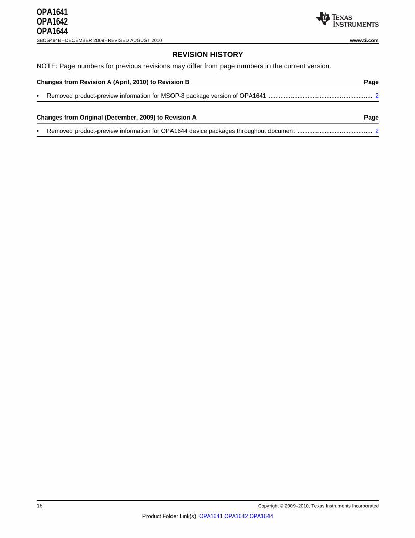
REVISION HISTORY
NOTE: Page numbers for previous revisions may differ from page numbers in the current version.
Changes from Revision A (April, 2010) to Revision B Page
• Removed product-preview information for MSOP-8 package version of OPA1641 ............................................................. 2
Changes from Original (December, 2009) to Revision A Page
• Removed product-preview information for OPA1644 device packages throughout document ............................................ 2
16 Copyright © 2009–2010, Texas Instruments Incorporated
Product Folder Link(s): OPA1641 OPA1642 OPA1644
PACKAGE OPTION ADDENDUM
www.ti.com 18-Oct-2013
Addendum-Page 1
PACKAGING INFORMATION
Orderable Device Status(1)
Package Type PackageDrawing
Pins PackageQty
Eco Plan(2)
Lead/Ball Finish(6)
MSL Peak Temp(3)
Op Temp (°C) Device Marking(4/5)
Samples
OPA1641AID ACTIVE SOIC D 8 75 Green (RoHS& no Sb/Br)
CU NIPDAU Level-2-260C-1 YEAR -40 to 85 O1641A
OPA1641AIDGKR ACTIVE VSSOP DGK 8 2500 Green (RoHS& no Sb/Br)
CU NIPDAUAG | Call TI Level-2-260C-1 YEAR -40 to 85 1641
OPA1641AIDGKT ACTIVE VSSOP DGK 8 250 Green (RoHS& no Sb/Br)
CU NIPDAUAG | Call TI Level-2-260C-1 YEAR -40 to 85 1641
OPA1641AIDR ACTIVE SOIC D 8 2500 Green (RoHS& no Sb/Br)
CU NIPDAU Level-2-260C-1 YEAR -40 to 85 O1641A
OPA1642AID ACTIVE SOIC D 8 75 Green (RoHS& no Sb/Br)
CU NIPDAU Level-2-260C-1 YEAR -40 to 85 O1642A
OPA1642AIDGKR ACTIVE VSSOP DGK 8 2500 Green (RoHS& no Sb/Br)
CU NIPDAUAG Level-2-260C-1 YEAR -40 to 85 1642
OPA1642AIDGKT ACTIVE VSSOP DGK 8 250 Green (RoHS& no Sb/Br)
CU NIPDAUAG Level-2-260C-1 YEAR -40 to 85 1642
OPA1642AIDR ACTIVE SOIC D 8 2500 Green (RoHS& no Sb/Br)
CU NIPDAU Level-2-260C-1 YEAR -40 to 85 O1642A
OPA1644AID ACTIVE SOIC D 14 50 Green (RoHS& no Sb/Br)
CU NIPDAU Level-2-260C-1 YEAR -40 to 85 O1644A
OPA1644AIDR ACTIVE SOIC D 14 2500 Green (RoHS& no Sb/Br)
CU NIPDAU Level-2-260C-1 YEAR -40 to 85 O1644A
OPA1644AIPW ACTIVE TSSOP PW 14 90 Green (RoHS& no Sb/Br)
CU NIPDAU Level-2-260C-1 YEAR -40 to 85 O1644A
OPA1644AIPWR ACTIVE TSSOP PW 14 2000 Green (RoHS& no Sb/Br)
CU NIPDAU Level-2-260C-1 YEAR -40 to 85 O1644A
(1) The marketing status values are defined as follows:ACTIVE: Product device recommended for new designs.LIFEBUY: TI has announced that the device will be discontinued, and a lifetime-buy period is in effect.NRND: Not recommended for new designs. Device is in production to support existing customers, but TI does not recommend using this part in a new design.PREVIEW: Device has been announced but is not in production. Samples may or may not be available.OBSOLETE: TI has discontinued the production of the device.
(2) Eco Plan - The planned eco-friendly classification: Pb-Free (RoHS), Pb-Free (RoHS Exempt), or Green (RoHS & no Sb/Br) - please check http://www.ti.com/productcontent for the latest availabilityinformation and additional product content details.TBD: The Pb-Free/Green conversion plan has not been defined.
PACKAGE OPTION ADDENDUM
www.ti.com 18-Oct-2013
Addendum-Page 2
Pb-Free (RoHS): TI's terms "Lead-Free" or "Pb-Free" mean semiconductor products that are compatible with the current RoHS requirements for all 6 substances, including the requirement thatlead not exceed 0.1% by weight in homogeneous materials. Where designed to be soldered at high temperatures, TI Pb-Free products are suitable for use in specified lead-free processes.Pb-Free (RoHS Exempt): This component has a RoHS exemption for either 1) lead-based flip-chip solder bumps used between the die and package, or 2) lead-based die adhesive used betweenthe die and leadframe. The component is otherwise considered Pb-Free (RoHS compatible) as defined above.Green (RoHS & no Sb/Br): TI defines "Green" to mean Pb-Free (RoHS compatible), and free of Bromine (Br) and Antimony (Sb) based flame retardants (Br or Sb do not exceed 0.1% by weightin homogeneous material)
(3) MSL, Peak Temp. - The Moisture Sensitivity Level rating according to the JEDEC industry standard classifications, and peak solder temperature.
(4) There may be additional marking, which relates to the logo, the lot trace code information, or the environmental category on the device.
(5) Multiple Device Markings will be inside parentheses. Only one Device Marking contained in parentheses and separated by a "~" will appear on a device. If a line is indented then it is a continuationof the previous line and the two combined represent the entire Device Marking for that device.
(6) Lead/Ball Finish - Orderable Devices may have multiple material finish options. Finish options are separated by a vertical ruled line. Lead/Ball Finish values may wrap to two lines if the finishvalue exceeds the maximum column width.
Important Information and Disclaimer:The information provided on this page represents TI's knowledge and belief as of the date that it is provided. TI bases its knowledge and belief on informationprovided by third parties, and makes no representation or warranty as to the accuracy of such information. Efforts are underway to better integrate information from third parties. TI has taken andcontinues to take reasonable steps to provide representative and accurate information but may not have conducted destructive testing or chemical analysis on incoming materials and chemicals.TI and TI suppliers consider certain information to be proprietary, and thus CAS numbers and other limited information may not be available for release.
In no event shall TI's liability arising out of such information exceed the total purchase price of the TI part(s) at issue in this document sold by TI to Customer on an annual basis.
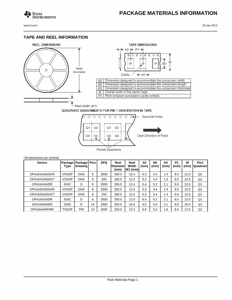
TAPE AND REEL INFORMATION
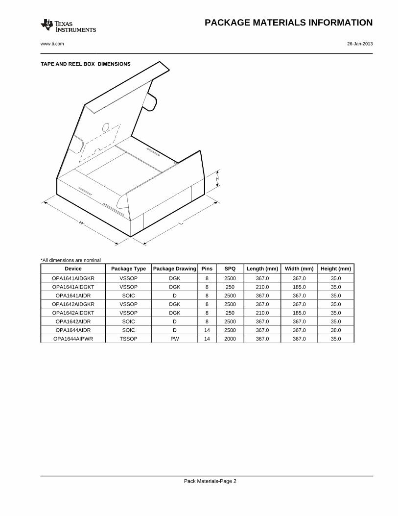
*All dimensions are nominal
Device PackageType
PackageDrawing
Pins SPQ ReelDiameter
(mm)
ReelWidth
W1 (mm)
A0(mm)
B0(mm)
K0(mm)
P1(mm)
W(mm)
Pin1Quadrant
OPA1641AIDGKR VSSOP DGK 8 2500 330.0 12.4 5.3 3.4 1.4 8.0 12.0 Q1
OPA1641AIDGKT VSSOP DGK 8 250 180.0 12.4 5.3 3.4 1.4 8.0 12.0 Q1
OPA1641AIDR SOIC D 8 2500 330.0 12.4 6.4 5.2 2.1 8.0 12.0 Q1
OPA1642AIDGKR VSSOP DGK 8 2500 330.0 12.4 5.3 3.4 1.4 8.0 12.0 Q1
OPA1642AIDGKT VSSOP DGK 8 250 180.0 12.4 5.3 3.4 1.4 8.0 12.0 Q1
OPA1642AIDR SOIC D 8 2500 330.0 12.4 6.4 5.2 2.1 8.0 12.0 Q1
OPA1644AIDR SOIC D 14 2500 330.0 16.4 6.5 9.0 2.1 8.0 16.0 Q1
OPA1644AIPWR TSSOP PW 14 2000 330.0 12.4 6.9 5.6 1.6 8.0 12.0 Q1
PACKAGE MATERIALS INFORMATION
www.ti.com 26-Jan-2013
Pack Materials-Page 1
*All dimensions are nominal
Device Package Type Package Drawing Pins SPQ Length (mm) Width (mm) Height (mm)
OPA1641AIDGKR VSSOP DGK 8 2500 367.0 367.0 35.0
OPA1641AIDGKT VSSOP DGK 8 250 210.0 185.0 35.0
OPA1641AIDR SOIC D 8 2500 367.0 367.0 35.0
OPA1642AIDGKR VSSOP DGK 8 2500 367.0 367.0 35.0
OPA1642AIDGKT VSSOP DGK 8 250 210.0 185.0 35.0
OPA1642AIDR SOIC D 8 2500 367.0 367.0 35.0
OPA1644AIDR SOIC D 14 2500 367.0 367.0 38.0
OPA1644AIPWR TSSOP PW 14 2000 367.0 367.0 35.0
PACKAGE MATERIALS INFORMATION
www.ti.com 26-Jan-2013
Pack Materials-Page 2
IMPORTANT NOTICE
Texas Instruments Incorporated and its subsidiaries (TI) reserve the right to make corrections, enhancements, improvements and otherchanges to its semiconductor products and services per JESD46, latest issue, and to discontinue any product or service per JESD48, latestissue. Buyers should obtain the latest relevant information before placing orders and should verify that such information is current andcomplete. All semiconductor products (also referred to herein as “components”) are sold subject to TI’s terms and conditions of salesupplied at the time of order acknowledgment.TI warrants performance of its components to the specifications applicable at the time of sale, in accordance with the warranty in TI’s termsand conditions of sale of semiconductor products. Testing and other quality control techniques are used to the extent TI deems necessaryto support this warranty. Except where mandated by applicable law, testing of all parameters of each component is not necessarilyperformed.TI assumes no liability for applications assistance or the design of Buyers’ products. Buyers are responsible for their products andapplications using TI components. To minimize the risks associated with Buyers’ products and applications, Buyers should provideadequate design and operating safeguards.TI does not warrant or represent that any license, either express or implied, is granted under any patent right, copyright, mask work right, orother intellectual property right relating to any combination, machine, or process in which TI components or services are used. Informationpublished by TI regarding third-party products or services does not constitute a license to use such products or services or a warranty orendorsement thereof. Use of such information may require a license from a third party under the patents or other intellectual property of thethird party, or a license from TI under the patents or other intellectual property of TI.Reproduction of significant portions of TI information in TI data books or data sheets is permissible only if reproduction is without alterationand is accompanied by all associated warranties, conditions, limitations, and notices. TI is not responsible or liable for such altereddocumentation. Information of third parties may be subject to additional restrictions.Resale of TI components or services with statements different from or beyond the parameters stated by TI for that component or servicevoids all express and any implied warranties for the associated TI component or service and is an unfair and deceptive business practice.TI is not responsible or liable for any such statements.Buyer acknowledges and agrees that it is solely responsible for compliance with all legal, regulatory and safety-related requirementsconcerning its products, and any use of TI components in its applications, notwithstanding any applications-related information or supportthat may be provided by TI. Buyer represents and agrees that it has all the necessary expertise to create and implement safeguards whichanticipate dangerous consequences of failures, monitor failures and their consequences, lessen the likelihood of failures that might causeharm and take appropriate remedial actions. Buyer will fully indemnify TI and its representatives against any damages arising out of the useof any TI components in safety-critical applications.In some cases, TI components may be promoted specifically to facilitate safety-related applications. With such components, TI’s goal is tohelp enable customers to design and create their own end-product solutions that meet applicable functional safety standards andrequirements. Nonetheless, such components are subject to these terms.No TI components are authorized for use in FDA Class III (or similar life-critical medical equipment) unless authorized officers of the partieshave executed a special agreement specifically governing such use.Only those TI components which TI has specifically designated as military grade or “enhanced plastic” are designed and intended for use inmilitary/aerospace applications or environments. Buyer acknowledges and agrees that any military or aerospace use of TI componentswhich have not been so designated is solely at the Buyer's risk, and that Buyer is solely responsible for compliance with all legal andregulatory requirements in connection with such use.TI has specifically designated certain components as meeting ISO/TS16949 requirements, mainly for automotive use. In any case of use ofnon-designated products, TI will not be responsible for any failure to meet ISO/TS16949.
Products ApplicationsAudio www.ti.com/audio Automotive and Transportation www.ti.com/automotiveAmplifiers amplifier.ti.com Communications and Telecom www.ti.com/communicationsData Converters dataconverter.ti.com Computers and Peripherals www.ti.com/computersDLP® Products www.dlp.com Consumer Electronics www.ti.com/consumer-appsDSP dsp.ti.com Energy and Lighting www.ti.com/energyClocks and Timers www.ti.com/clocks Industrial www.ti.com/industrialInterface interface.ti.com Medical www.ti.com/medicalLogic logic.ti.com Security www.ti.com/securityPower Mgmt power.ti.com Space, Avionics and Defense www.ti.com/space-avionics-defenseMicrocontrollers microcontroller.ti.com Video and Imaging www.ti.com/videoRFID www.ti-rfid.comOMAP Applications Processors www.ti.com/omap TI E2E Community e2e.ti.comWireless Connectivity www.ti.com/wirelessconnectivity
Mailing Address: Texas Instruments, Post Office Box 655303, Dallas, Texas 75265Copyright © 2015, Texas Instruments Incorporated