Embed Size (px)
Citation preview

Op Amp based Applications
XMUT303 Analogue Electronics

• Op Amp based Rectifier:
• Half-wave rectifier, full-wave rectifier, precision peak
detector.
• Comparator:
• Voltage comparator, Schmitt trigger.
• Op Amp based Oscillator:
• Wien-Bridge oscillator, phase-shift oscillator, application
specific oscillators.
Topics
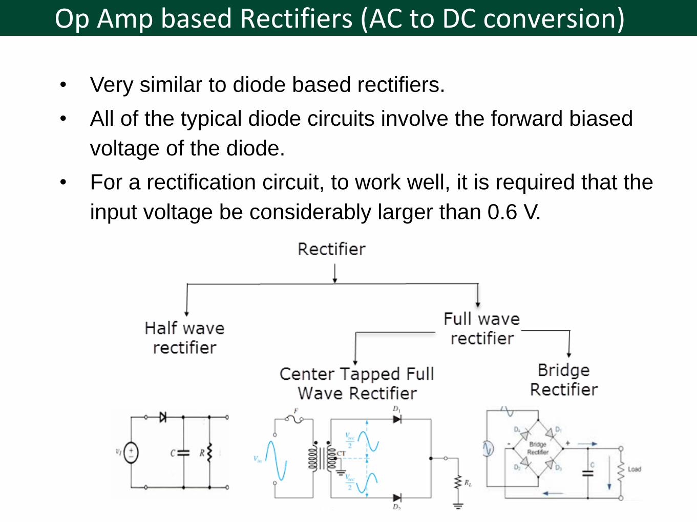
Op Amp based Rectifiers (AC to DC conversion)
• Very similar to diode based rectifiers.
• All of the typical diode circuits involve the forward biased
voltage of the diode.
• For a rectification circuit, to work well, it is required that the
input voltage be considerably larger than 0.6 V.
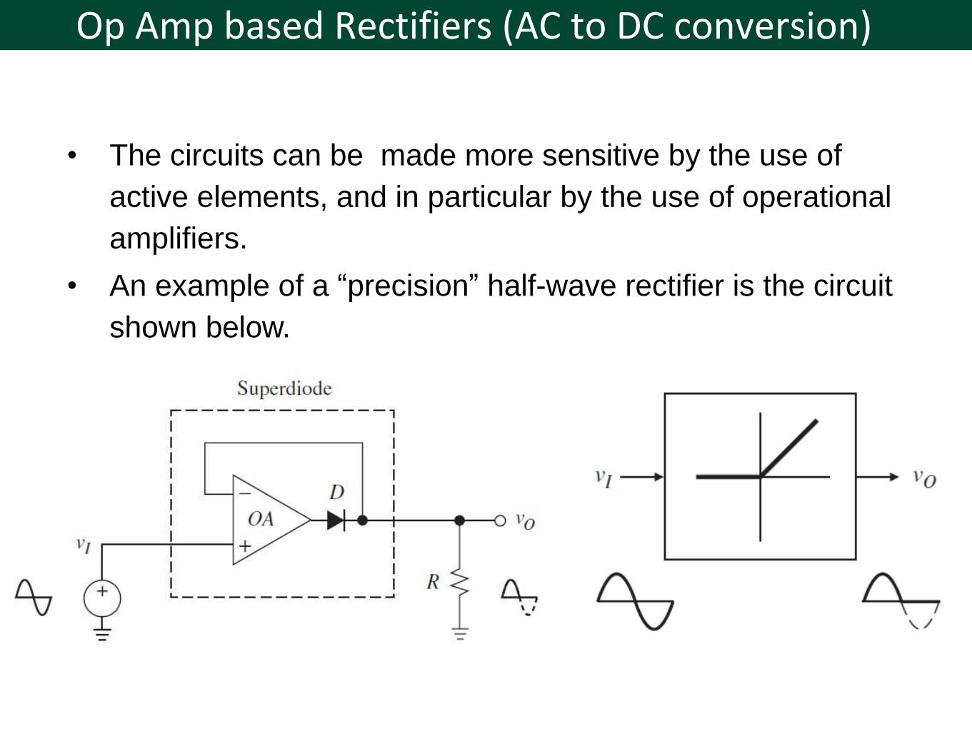
Op Amp based Rectifiers (AC to DC conversion)
• The circuits can be made more sensitive by the use of
active elements, and in particular by the use of operational
amplifiers.
• An example of a “precision” half-wave rectifier is the circuit
shown below.
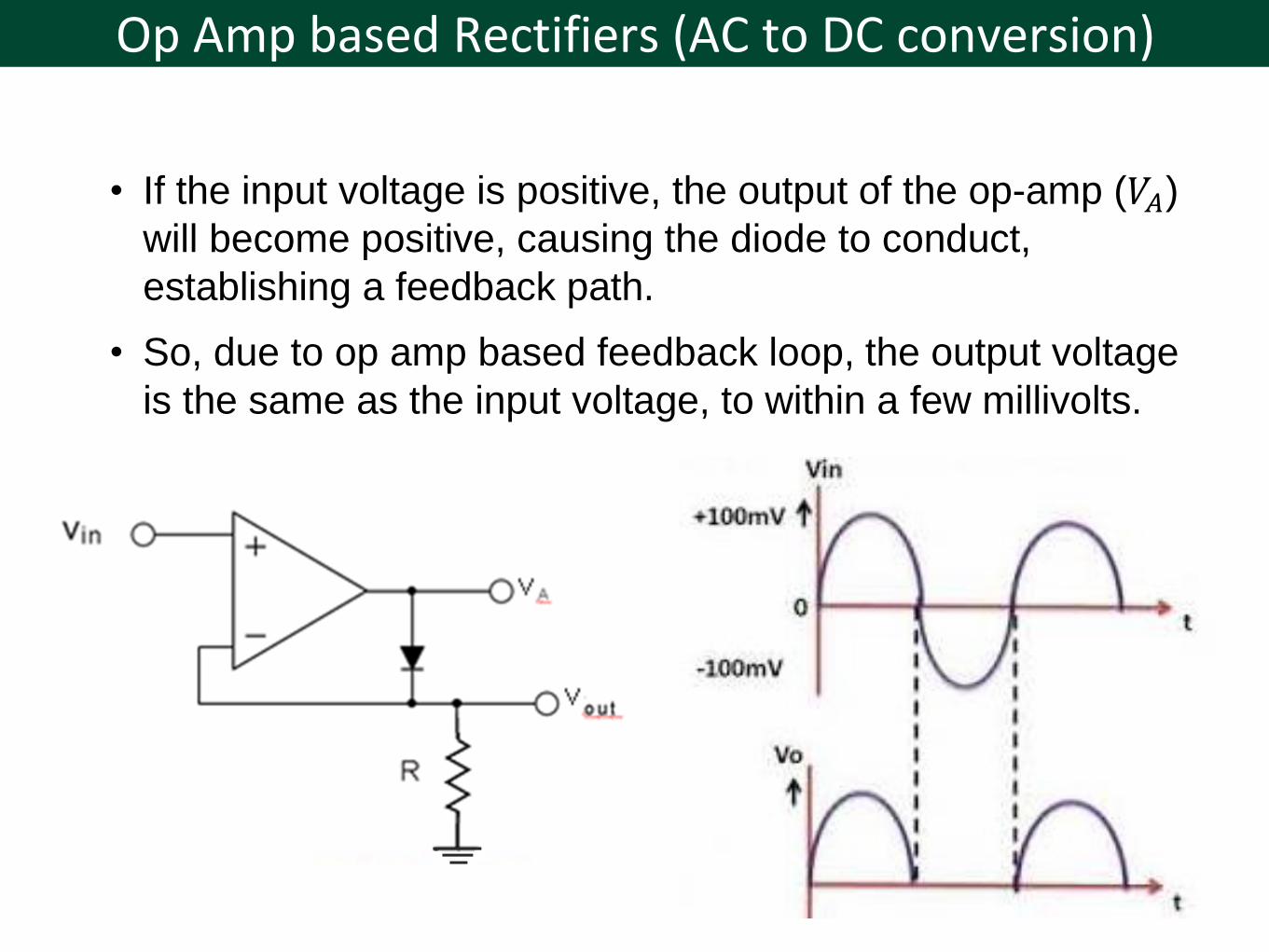
Op Amp based Rectifiers (AC to DC conversion)
• If the input voltage is positive, the output of the op-amp (𝑉𝐴)
will become positive, causing the diode to conduct,
establishing a feedback path.
• So, due to op amp based feedback loop, the output voltage
is the same as the input voltage, to within a few millivolts.

Op Amp based Rectifiers (AC to DC conversion)
• If the input voltage is negative, the op-amp output 𝑉𝐴 will be
a large negative voltage (its saturation limit), no current will
flow through the diode, and so the output voltage will be
zero.
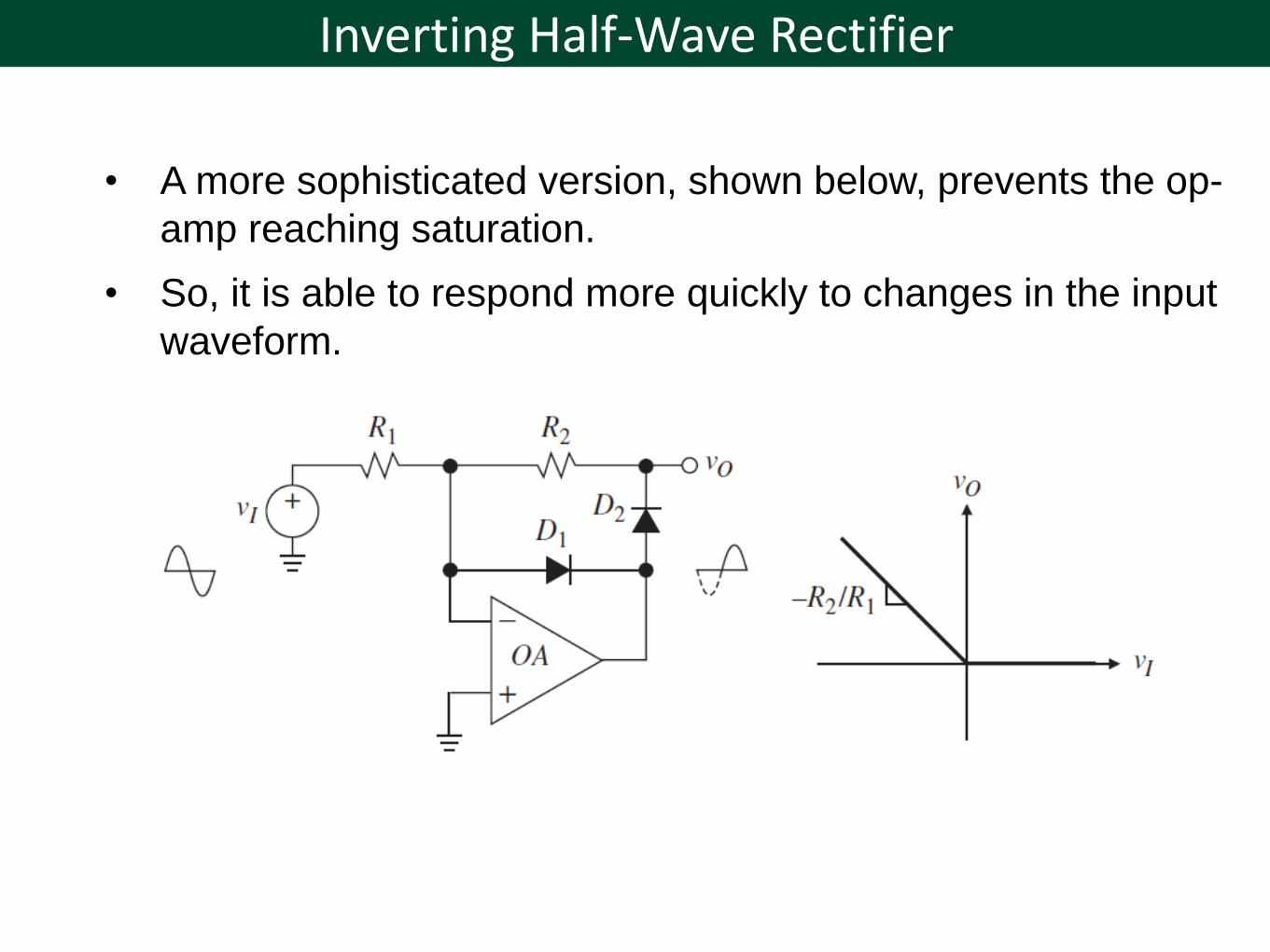
Inverting Half-Wave Rectifier
• A more sophisticated version, shown below, prevents the op-
amp reaching saturation.
• So, it is able to respond more quickly to changes in the input
waveform.
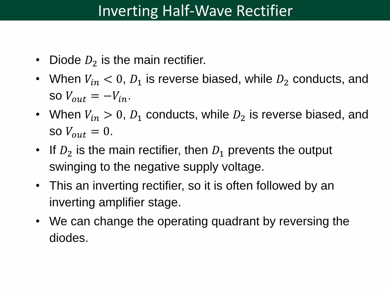
Inverting Half-Wave Rectifier
• Diode 𝐷2 is the main rectifier.
• When 𝑉𝑖𝑛 < 0, 𝐷1 is reverse biased, while 𝐷2 conducts, and
so 𝑉𝑜𝑢𝑡 = −𝑉𝑖𝑛.
• When 𝑉𝑖𝑛 > 0, 𝐷1 conducts, while 𝐷2 is reverse biased, and
so 𝑉𝑜𝑢𝑡 = 0.
• If 𝐷2 is the main rectifier, then 𝐷1 prevents the output
swinging to the negative supply voltage.
• This an inverting rectifier, so it is often followed by an
inverting amplifier stage.
• We can change the operating quadrant by reversing the
diodes.

• One way of synthesising a full-wave rectifier is by combining
the signal itself with its inverted half-wave rectified version in
a 1-to-2 ratio, as shown below.
• The first op-amp is a half-wave rectifier similar to that shown
previously but with diodes in the opposite direction.
Full-Wave Rectifier
Full-Wave Rectifier
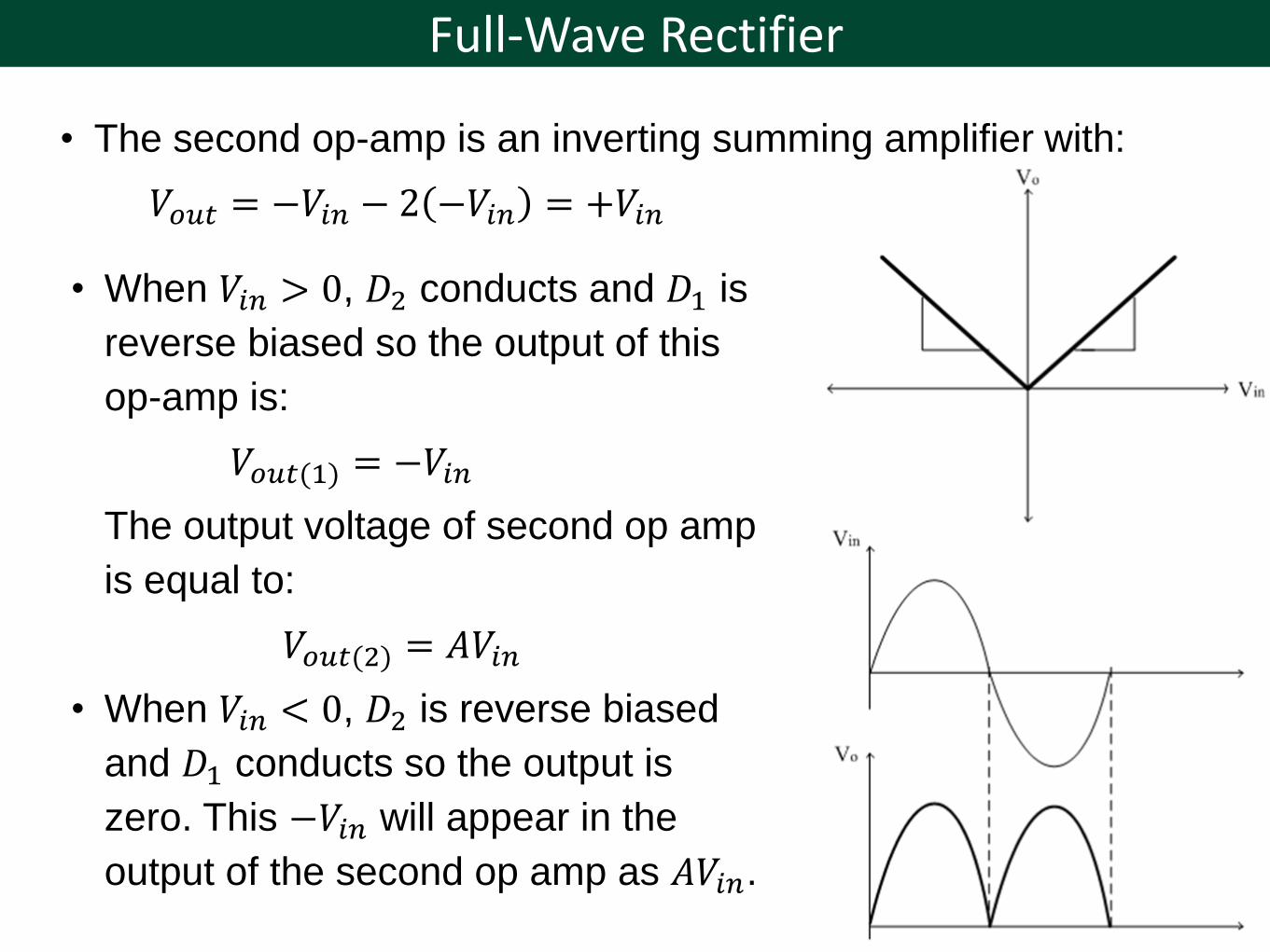
• The second op-amp is an inverting summing amplifier with:
𝑉𝑜𝑢𝑡 = −𝑉𝑖𝑛 − 2 −𝑉𝑖𝑛 = +𝑉𝑖𝑛
• When 𝑉𝑖𝑛 > 0, 𝐷2 conducts and 𝐷1 is
reverse biased so the output of this
op-amp is:
𝑉𝑜𝑢𝑡(1) = −𝑉𝑖𝑛
The output voltage of second op amp
is equal to:
𝑉𝑜𝑢𝑡(2) = 𝐴𝑉𝑖𝑛
• When 𝑉𝑖𝑛 < 0, 𝐷2 is reverse biased
and 𝐷1 conducts so the output is
zero. This −𝑉𝑖𝑛 will appear in the
output of the second op amp as 𝐴𝑉𝑖𝑛.
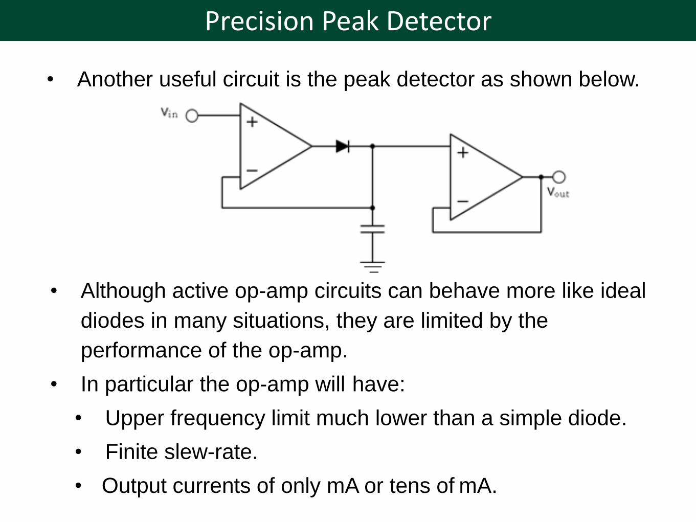
• Another useful circuit is the peak detector as shown below.
Precision Peak Detector
• Although active op-amp circuits can behave more like ideal
diodes in many situations, they are limited by the
performance of the op-amp.
• In particular the op-amp will have:
• Upper frequency limit much lower than a simple diode.
• Finite slew-rate.
• Output currents of only mA or tens of mA.
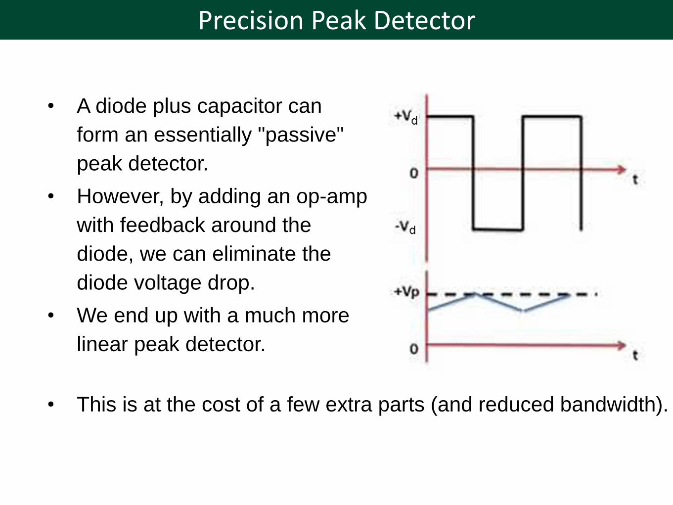
• A diode plus capacitor can
form an essentially "passive"
peak detector.
• However, by adding an op-amp
with feedback around the
diode, we can eliminate the
diode voltage drop.
• We end up with a much more
linear peak detector.
Precision Peak Detector
• This is at the cost of a few extra parts (and reduced bandwidth).

Voltage Comparator
• A voltage comparator compares the voltage at one input
against the voltage at the other input.
• The symbol used is the same as an op-amp as an op-amp
can be used to make a comparator.
• If 𝑉𝑃 > 𝑉𝑁 then 𝑉𝑂 = 𝑉𝑂𝐻
• If 𝑉𝑃 < 𝑉𝑁 then 𝑉𝑂 = 𝑉𝑂𝐿
• Voltage transfer curve (VTC) of comparator: 𝑉𝐷 = 𝑉𝑃 − 𝑉𝑁.

• In general, the op amp is designed to be a linear device and
is not optimised for rapid rail-to-rail switching.
Response Time
• When using an op-amp as a comparator, we are relying on the
open-loop gain to provide the two different output states.
• These are basically the alternate saturation levels that are
close to the op-amp rail voltages.
• The internal stages have significant parasitic capacitance
(or the op-amp has added capacitance to provide
stability).
• This coupled with the fact that the output transistors are
saturated results in that significant time is required for the
output to change state.
• The comparator speed is characterised in terms of
response time which is often also stated as propagation
delay (𝑇𝑃𝐷).
• Special comparator devices are available with low
propagation delays, fast slew rates and digital outputs.
• One example is the LM311 comparator op-amp which
we will look at soon.
Response Time
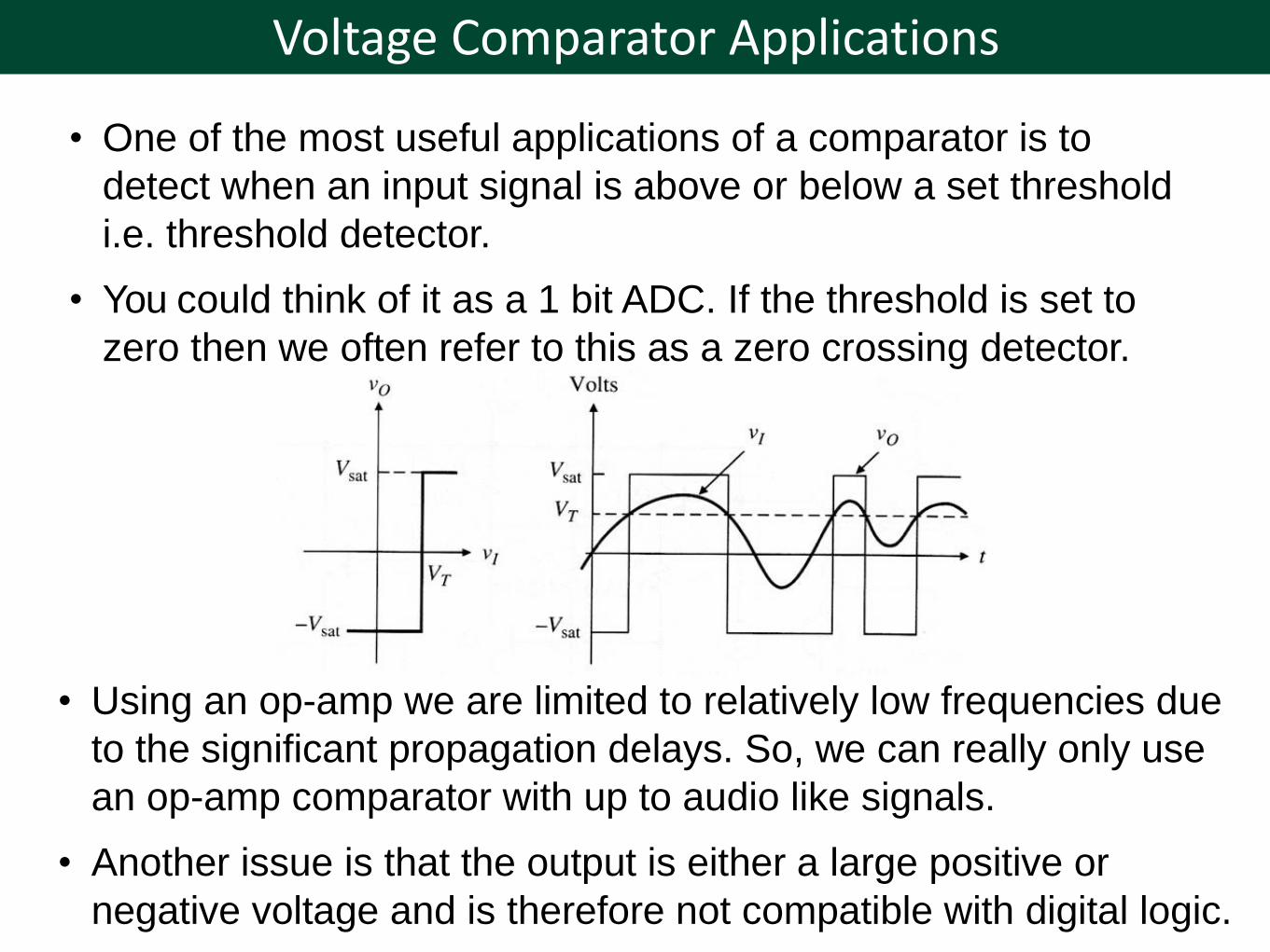
• One of the most useful applications of a comparator is to
detect when an input signal is above or below a set threshold
i.e. threshold detector.
• You could think of it as a 1 bit ADC. If the threshold is set to
zero then we often refer to this as a zero crossing detector.
Voltage Comparator Applications
• Using an op-amp we are limited to relatively low frequencies due
to the significant propagation delays. So, we can really only use
an op-amp comparator with up to audio like signals.
• Another issue is that the output is either a large positive or
negative voltage and is therefore not compatible with digital logic.

Simplified diagram
LM311 Voltage Comparator
LM311 is a popular voltage comparator that has an open collector
transistor as the output stage.
• If 𝑉𝑃 > 𝑉𝑁, then 𝑄𝑂 (the output transistor) is off.
• If 𝑉𝑃 < 𝑉𝑁, then 𝑄𝑂 is on.
LM311 Voltage Comparator
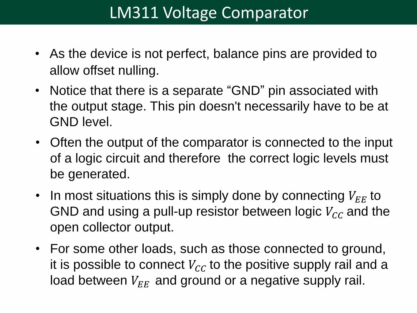
• As the device is not perfect, balance pins are provided to
allow offset nulling.
• Notice that there is a separate “GND” pin associated with
the output stage. This pin doesn't necessarily have to be at
GND level.
• Often the output of the comparator is connected to the input
of a logic circuit and therefore the correct logic levels must
be generated.
• In most situations this is simply done by connecting 𝑉𝐸𝐸 to
GND and using a pull-up resistor between logic 𝑉𝐶𝐶 and the
open collector output.
• For some other loads, such as those connected to ground,
it is possible to connect 𝑉𝐶𝐶 to the positive supply rail and a
load between 𝑉𝐸𝐸 and ground or a negative supply rail.
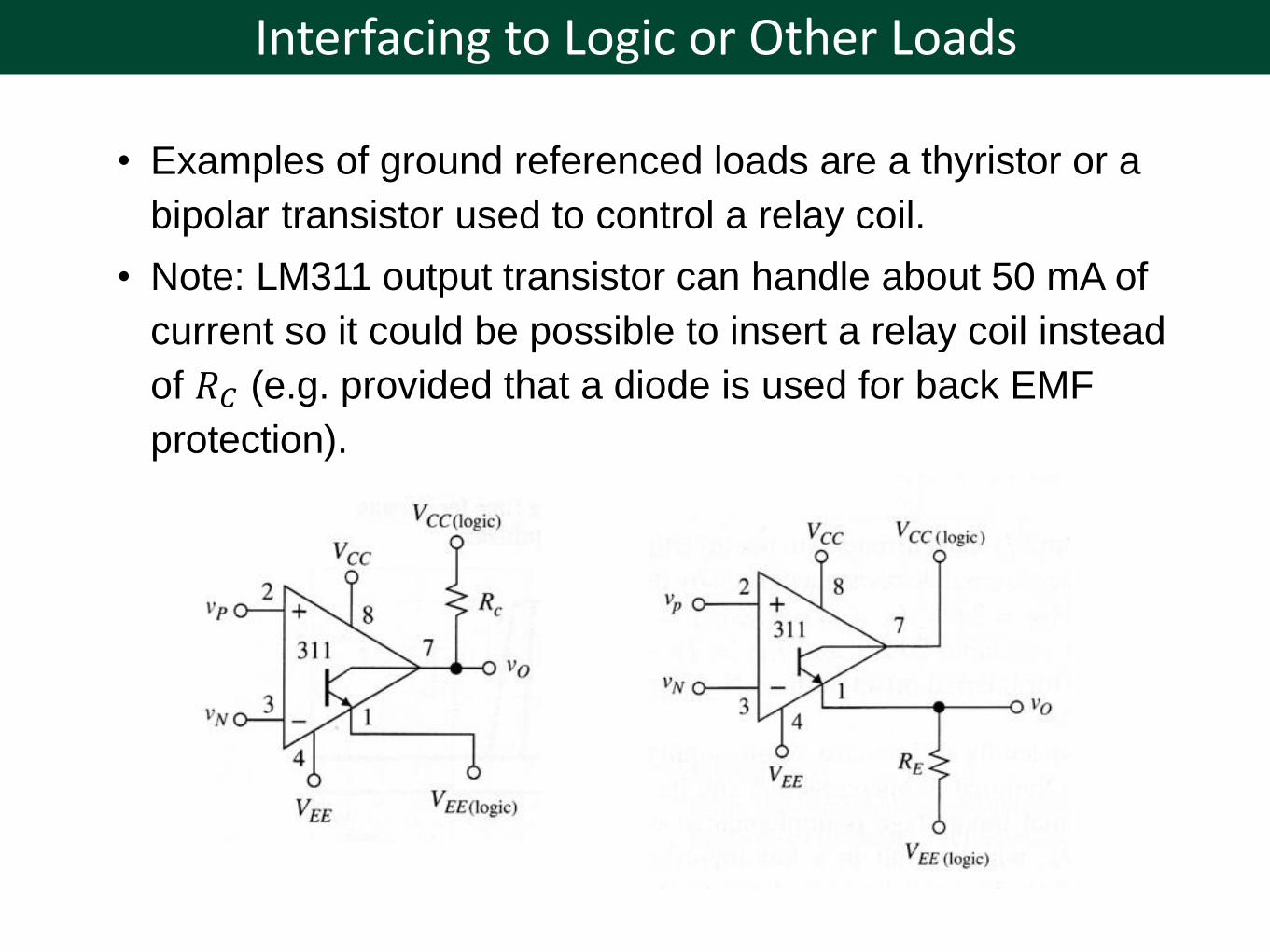
Interfacing to Logic or Other Loads
• Examples of ground referenced loads are a thyristor or a
bipolar transistor used to control a relay coil.
• Note: LM311 output transistor can handle about 50 mA of
current so it could be possible to insert a relay coil instead
of 𝑅𝐶 (e.g. provided that a diode is used for back EMF
protection).
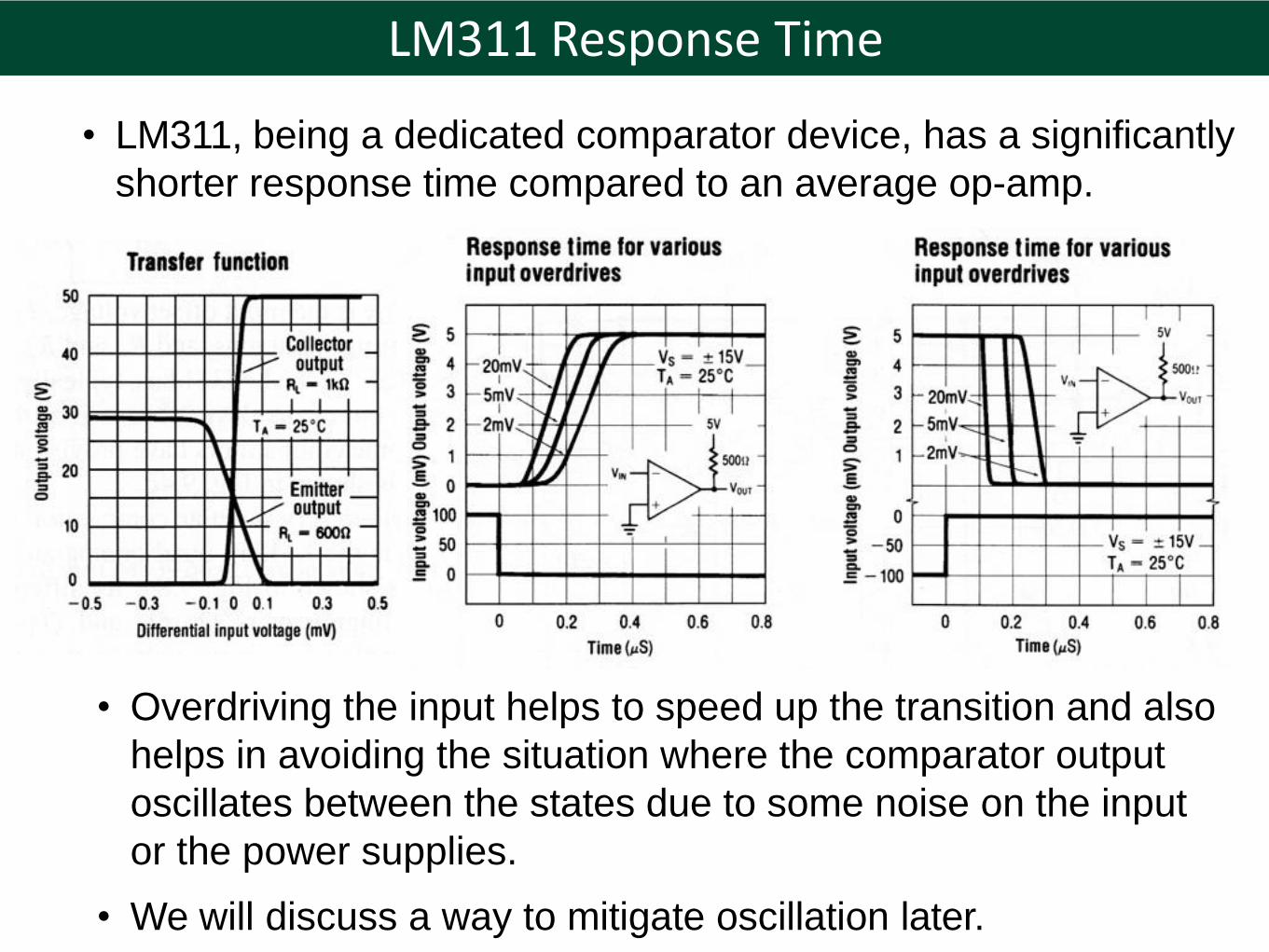
• LM311, being a dedicated comparator device, has a significantly
shorter response time compared to an average op-amp.
LM311 Response Time
• Overdriving the input helps to speed up the transition and also
helps in avoiding the situation where the comparator output
oscillates between the states due to some noise on the input
or the power supplies.
• We will discuss a way to mitigate oscillation later.
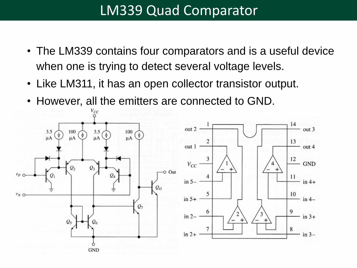
• The LM339 contains four comparators and is a useful device
when one is trying to detect several voltage levels.
• Like LM311, it has an open collector transistor output.
• However, all the emitters are connected to GND.
LM339 Quad Comparator
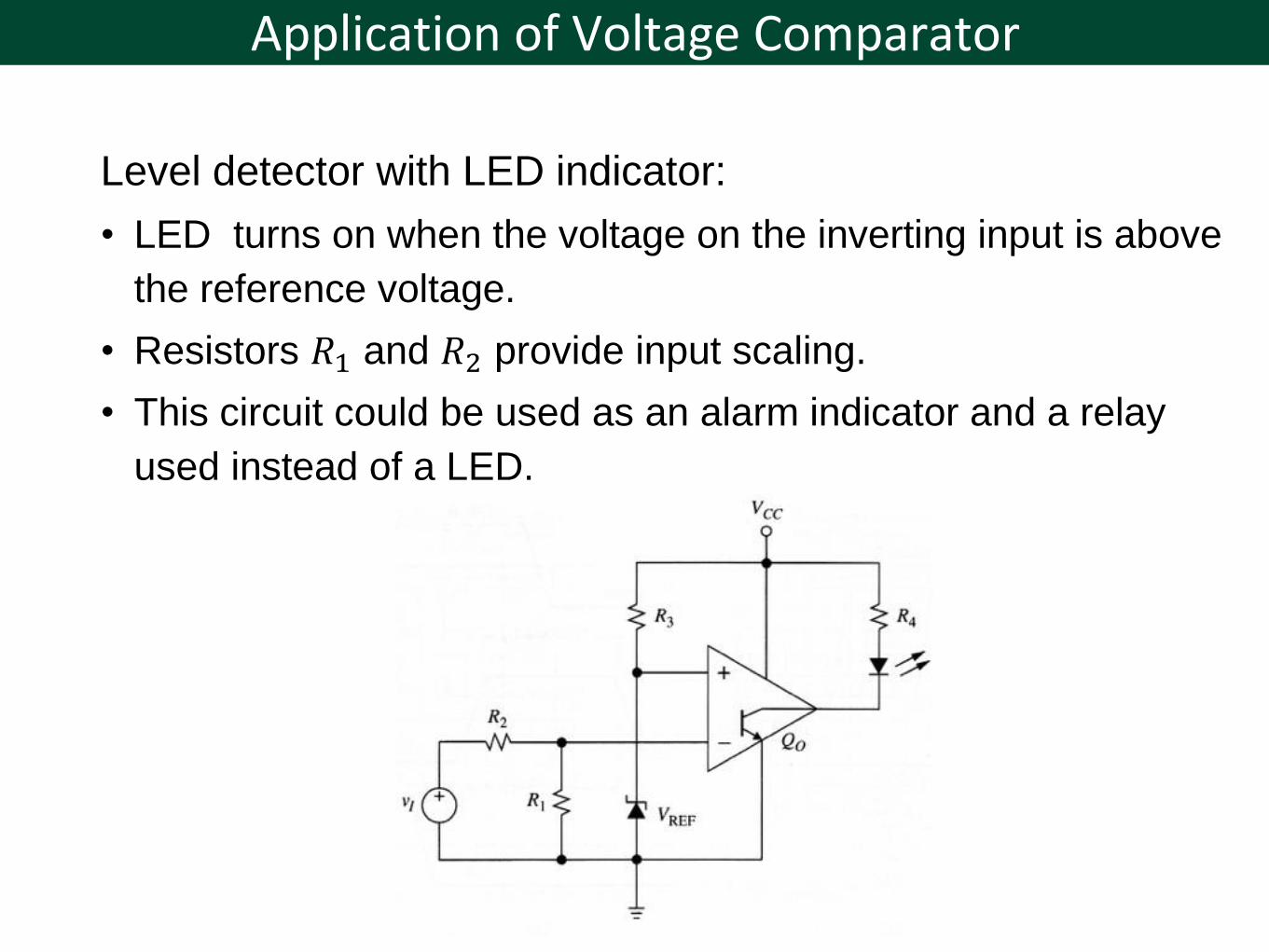
Level detector with LED indicator:
• LED turns on when the voltage on the inverting input is above
the reference voltage.
• Resistors 𝑅1 and 𝑅2 provide input scaling.
• This circuit could be used as an alarm indicator and a relay
used instead of a LED.
Application of Voltage Comparator
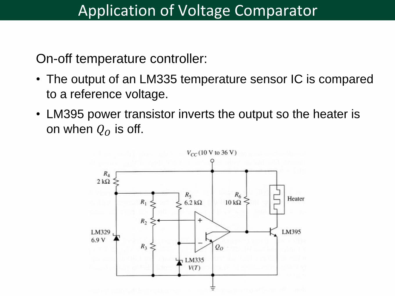
On-off temperature controller:
• The output of an LM335 temperature sensor IC is compared
to a reference voltage.
• LM395 power transistor inverts the output so the heater is
on when 𝑄𝑂 is off.
Application of Voltage Comparator
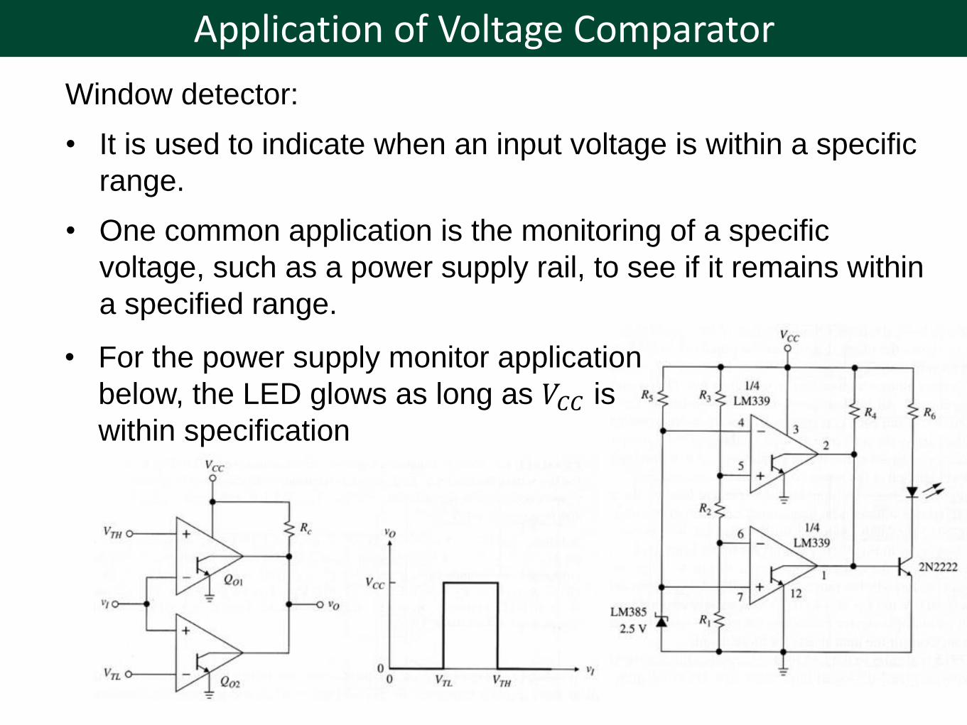
Window detector:
• It is used to indicate when an input voltage is within a specific
range.
• One common application is the monitoring of a specific
voltage, such as a power supply rail, to see if it remains within
a specified range.
Application of Voltage Comparator
• For the power supply monitor application
below, the LED glows as long as 𝑉𝐶𝐶 is
within specification

Bar graph display:
• It typically can be used to visually
represent a signal.
• It can be easily made with a string
of comparators and a voltage
divider chain.
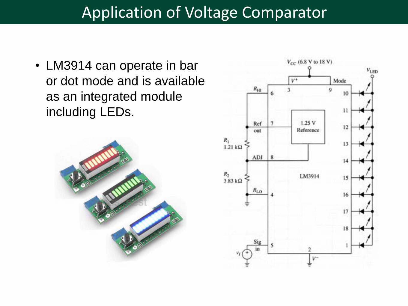
• LM3914 is a IC specifically
designed as a voltage level
indicator.
• This is specially used as a visual
unit (VU) meter in the audio
systems.
Application of Voltage Comparator
Application of Voltage Comparator
• LM3914 can operate in bar
or dot mode and is available
as an integrated module
including LEDs.

• As before, a potential problem with a comparator is that when the
reference and threshold voltages are close, there is the possibility
of oscillations (chatters) between the two output states.
• This is especially true when there is noise on the input signal.
Schmitt Triggers and Hysteresis
• A way to overcome this is to provide hysteresis and this is
done by adding positive feedback via resistors.
• The circuit above uses a voltage divider to provide positive
feedback around the op-amp.
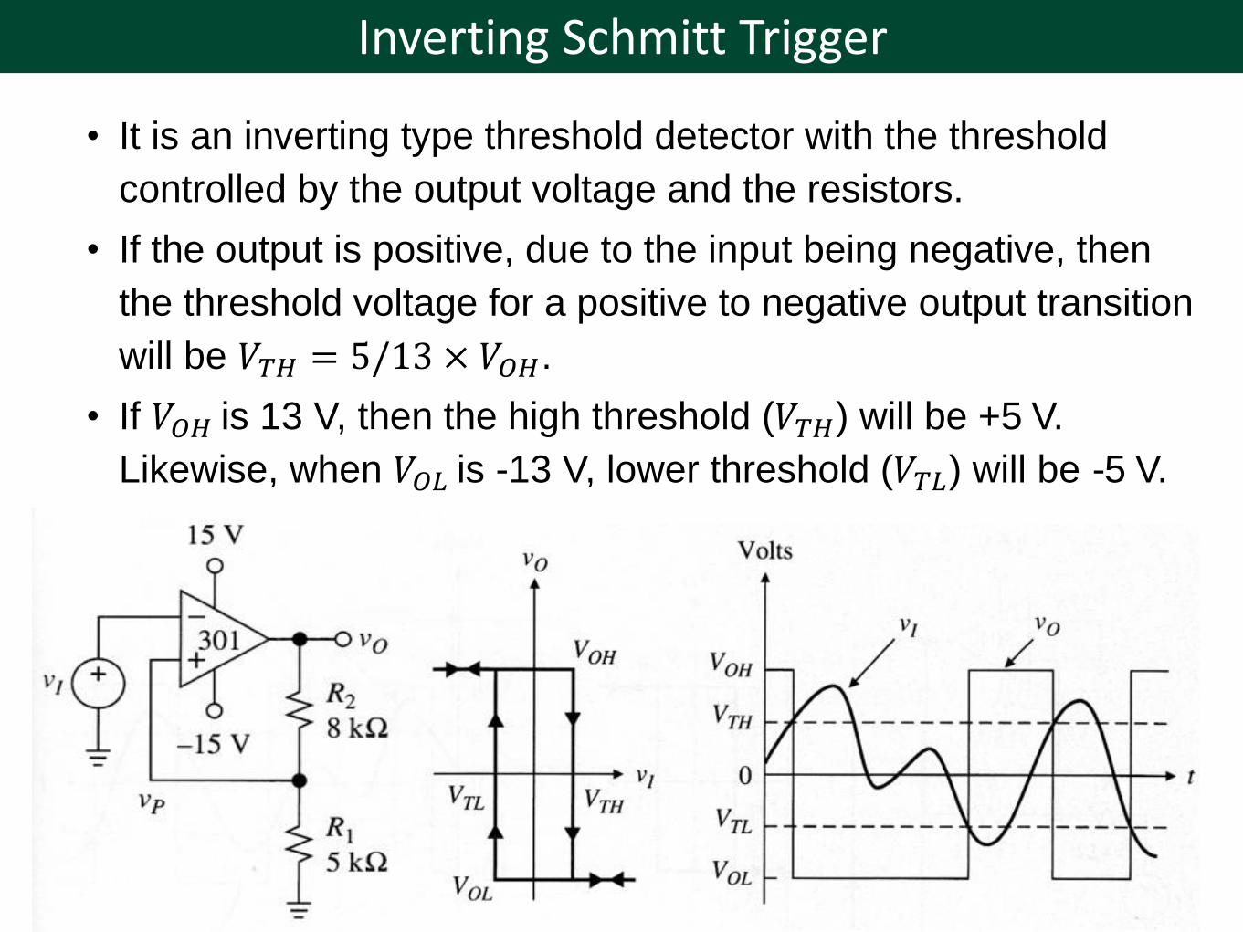
Inverting Schmitt Trigger
• It is an inverting type threshold detector with the threshold
controlled by the output voltage and the resistors.
• If the output is positive, due to the input being negative, then
the threshold voltage for a positive to negative output transition
will be 𝑉𝑇𝐻 = 5/13 × 𝑉𝑂𝐻.
• If 𝑉𝑂𝐻 is 13 V, then the high threshold (𝑉𝑇𝐻) will be +5 V.
Likewise, when 𝑉𝑂𝐿 is -13 V, lower threshold (𝑉𝑇𝐿) will be -5 V.
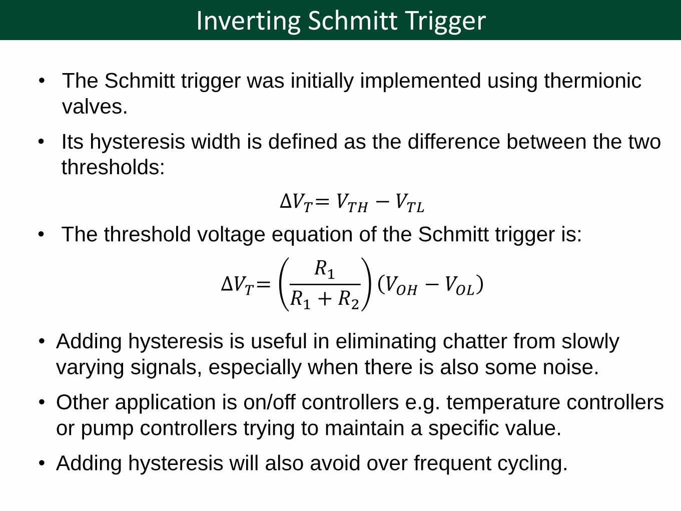
• The Schmitt trigger was initially implemented using thermionic
valves.
• Its hysteresis width is defined as the difference between the two
thresholds:
∆𝑉𝑇= 𝑉𝑇𝐻 − 𝑉𝑇𝐿
• The threshold voltage equation of the Schmitt trigger is:
∆𝑉𝑇=𝑅1
𝑅1 + 𝑅2𝑉𝑂𝐻 − 𝑉𝑂𝐿
• Adding hysteresis is useful in eliminating chatter from slowly
varying signals, especially when there is also some noise.
• Other application is on/off controllers e.g. temperature controllers
or pump controllers trying to maintain a specific value.
• Adding hysteresis will also avoid over frequent cycling.
Inverting Schmitt Trigger

Non-Inverting Schmitt Trigger
• For non-inverting Schmitt trigger, 𝑉𝐼 is now applied at the non-
inverting input. Notice its VTC is counter clockwise.
• If the output voltage is initially negative (due to 𝑉𝑖 previously
being very negative), then in order for the output to change to
positive, we must apply an input voltage (𝑉𝑇𝐻) that will cause
𝑉𝑃 to become slightly larger than 𝑉𝑁.
Non-Inverting Schmitt Trigger
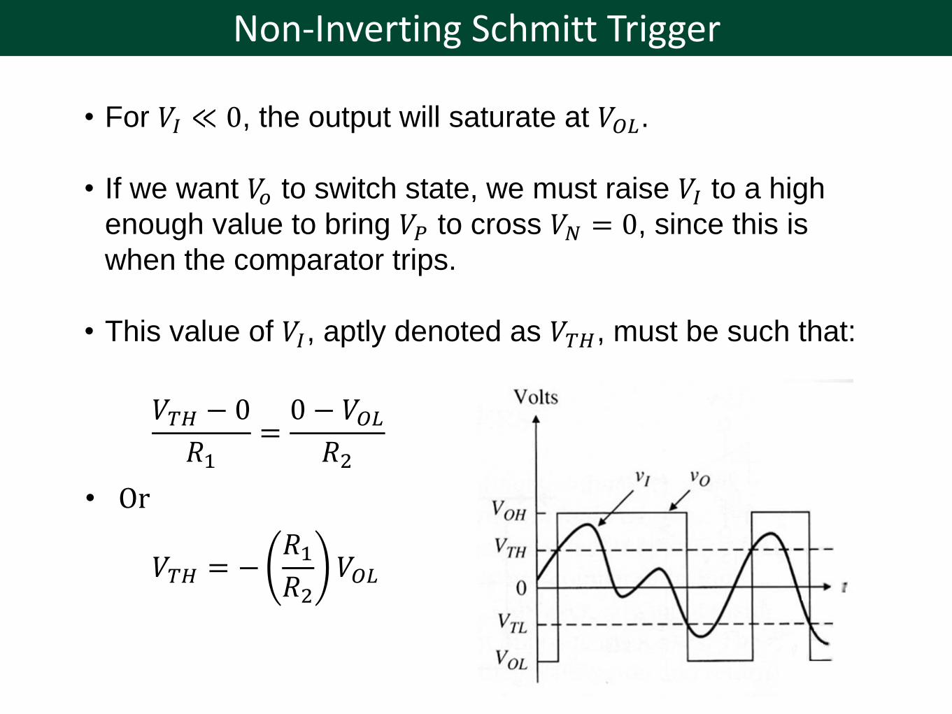
• For 𝑉𝐼 ≪ 0, the output will saturate at 𝑉𝑂𝐿.
• If we want 𝑉𝑜 to switch state, we must raise 𝑉𝐼 to a high
enough value to bring 𝑉𝑃 to cross 𝑉𝑁 = 0, since this is
when the comparator trips.
• This value of 𝑉𝐼, aptly denoted as 𝑉𝑇𝐻, must be such that:
𝑉𝑇𝐻 − 0
𝑅1=0 − 𝑉𝑂𝐿𝑅2
• Or
𝑉𝑇𝐻 = −𝑅1𝑅2
𝑉𝑂𝐿
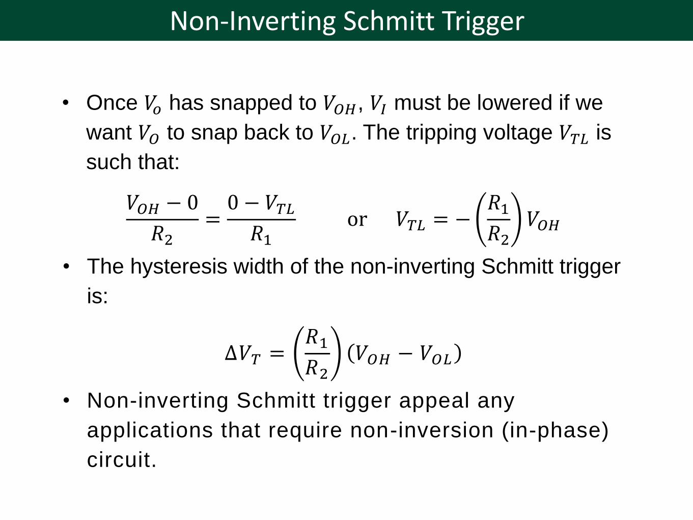
Non-Inverting Schmitt Trigger
• Once 𝑉𝑜 has snapped to 𝑉𝑂𝐻, 𝑉𝐼 must be lowered if we
want 𝑉𝑂 to snap back to 𝑉𝑂𝐿. The tripping voltage 𝑉𝑇𝐿 is
such that:
𝑉𝑂𝐻 − 0
𝑅2=0 − 𝑉𝑇𝐿𝑅1
or 𝑉𝑇𝐿 = −𝑅1𝑅2
𝑉𝑂𝐻
• The hysteresis width of the non-inverting Schmitt trigger
is:
∆𝑉𝑇 =𝑅1𝑅2
𝑉𝑂𝐻 − 𝑉𝑂𝐿
• Non-inverting Schmitt trigger appeal any
applications that require non-inversion (in-phase)
circuit.
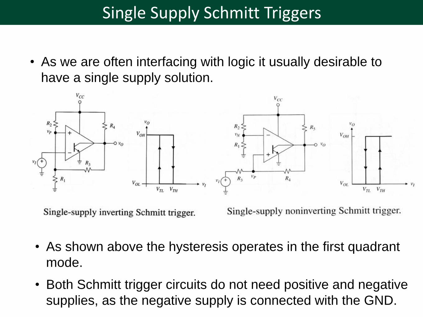
• As we are often interfacing with logic it usually desirable to
have a single supply solution.
Single Supply Schmitt Triggers
• As shown above the hysteresis operates in the first quadrant
mode.
• Both Schmitt trigger circuits do not need positive and negative
supplies, as the negative supply is connected with the GND.
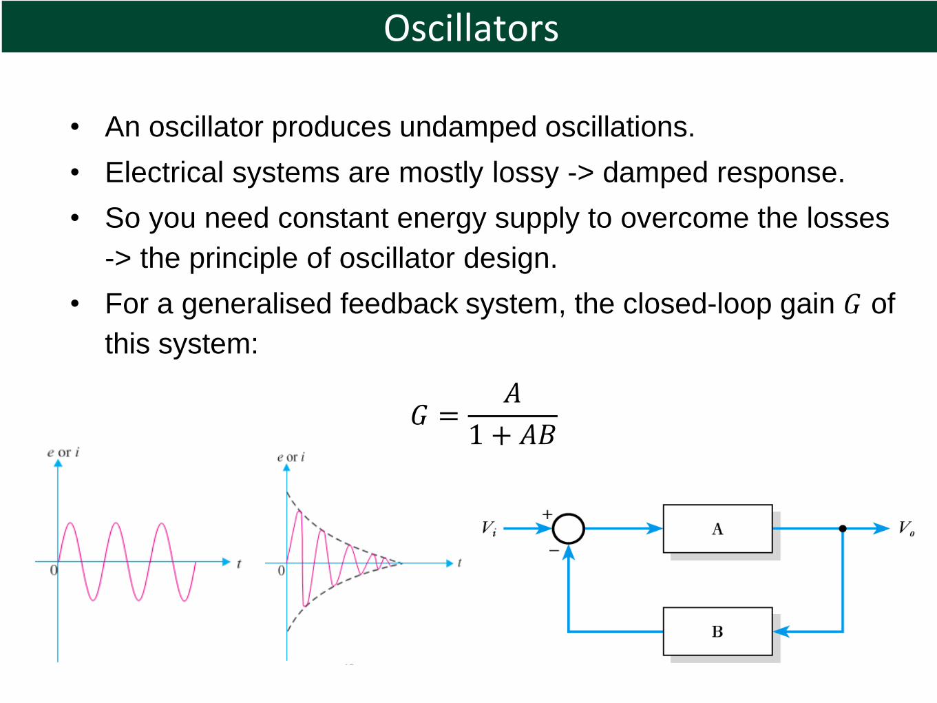
Oscillators
• An oscillator produces undamped oscillations.
• Electrical systems are mostly lossy -> damped response.
• So you need constant energy supply to overcome the losses
-> the principle of oscillator design.
• For a generalised feedback system, the closed-loop gain 𝐺 of
this system:
𝐺 =𝐴
1 + 𝐴𝐵
Barkhausen Criterion
• Looking at the expression for feedback system:
𝐺 =𝐴
1 + 𝐴𝐵
• We note that when 𝐴𝐵 = −1, |𝐴𝐵| = 1 with phase angle of
180°, the gain is infinite e.g. this represents the condition
for oscillation.
• The requirements for oscillation are described by the
Barkhausen criterion:
• The magnitude of the loop gain 𝐴𝐵 must be 1.
• The phase shift of the loop gain 𝐴𝐵 must be 360°.
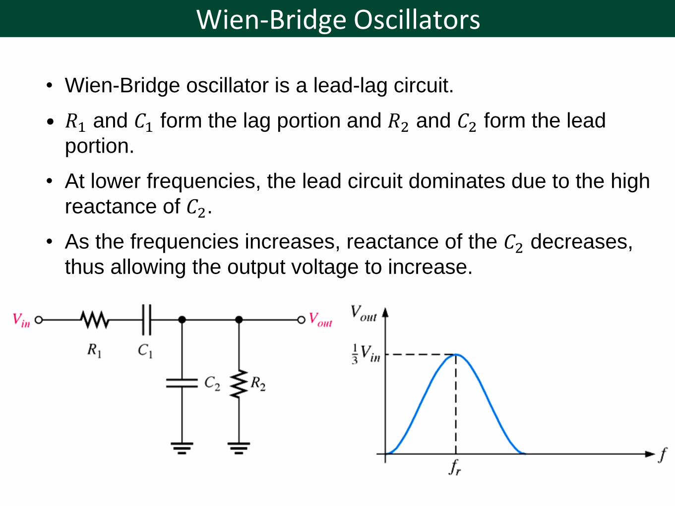
• Wien-Bridge oscillator is a lead-lag circuit.
• 𝑅1 and 𝐶1 form the lag portion and 𝑅2 and 𝐶2 form the lead
portion.
• At lower frequencies, the lead circuit dominates due to the high
reactance of 𝐶2.
• As the frequencies increases, reactance of the 𝐶2 decreases,
thus allowing the output voltage to increase.
Wien-Bridge Oscillators
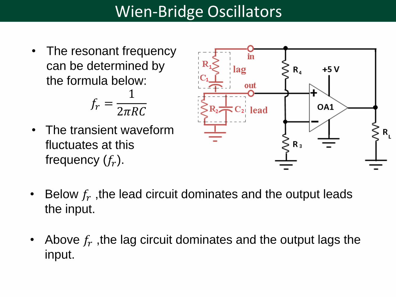
• The resonant frequency
can be determined by
the formula below:
𝑓𝑟 =1
2𝜋𝑅𝐶
• The transient waveform
fluctuates at this
frequency (𝑓𝑟).
Wien-Bridge Oscillators
• Below 𝑓𝑟 ,the lead circuit dominates and the output leads
the input.
• Above 𝑓𝑟 ,the lag circuit dominates and the output lags the
input.

Analysis of Oscillator
• The Wien Bridge uses two RC networks to produce the
required phase shift.
• The example oscillator circuit uses a single supply op-amp
with 𝑉𝐶𝐶 = +5 V and 𝑉𝐸𝐸 = GND.
• It is intended to oscillate between 0 and 5 V.
• The oscillator would vary symmetrically about zero as the
circuit is powered with 5 V single supply.
• Note the use of both positive and negative feedback.
Analysis of Oscillator
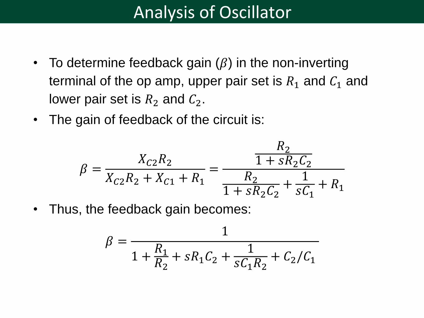
• To determine feedback gain (𝛽) in the non-inverting
terminal of the op amp, upper pair set is 𝑅1 and 𝐶1 and
lower pair set is 𝑅2 and 𝐶2.
• The gain of feedback of the circuit is:
𝛽 =𝑋𝐶2𝑅2
𝑋𝐶2𝑅2 + 𝑋𝐶1 + 𝑅1=
𝑅21 + 𝑠𝑅2𝐶2
𝑅21 + 𝑠𝑅2𝐶2
+1𝑠𝐶1
+ 𝑅1
• Thus, the feedback gain becomes:
𝛽 =1
1 +𝑅1𝑅2
+ 𝑠𝑅1𝐶2 +1
𝑠𝐶1𝑅2+ 𝐶2/𝐶1

Analysis of Oscillator
• In order to have a phase shift of zero, we have 𝑅1 = 𝑅2 = 𝑅
and 𝐶1 = 𝐶2 = 𝐶
𝛽 =1
1 +𝑅𝑅+ 𝑠𝑅𝐶 +
1𝑠𝑅𝐶
+ 𝐶/𝐶=
1
3 + 𝑠𝑅𝐶 +1
𝑠𝑅𝐶• This happens at s = 𝑗𝜔 = 𝑗/𝑅𝐶, we obtain:
𝛽 =1
3 + 𝑗 − 𝑗=1
3
• Thus, the system loop gain of oscillator circuit (𝐺) is found
from:
𝐺 = 𝑎𝛽 = 𝑎 1/3 = 𝑎/3
• If 𝐺 = 3, constant amplitude
oscillations.
• If 𝐺 < 3, oscillations attenuate.
• If 𝐺 > 3, oscillations amplify.
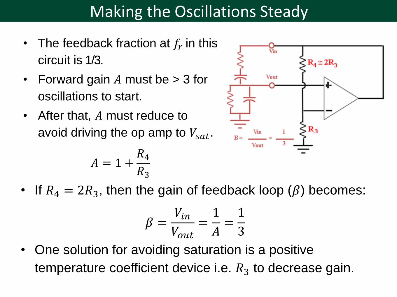
• If 𝑅4 = 2𝑅3, then the gain of feedback loop (𝛽) becomes:
𝛽 =𝑉𝑖𝑛𝑉𝑜𝑢𝑡
=1
𝐴=1
3
• One solution for avoiding saturation is a positive
temperature coefficient device i.e. 𝑅3 to decrease gain.
Making the Oscillations Steady
• The feedback fraction at 𝑓𝑟 in this
circuit is 1/3.
• Forward gain 𝐴 must be > 3 for
oscillations to start.
• After that, 𝐴 must reduce to
avoid driving the op amp to 𝑉𝑠𝑎𝑡.
𝐴 = 1 +𝑅4𝑅3

Making the Oscillations Steady
• Add a diode network to keep circuit around 𝐺 = 3.
• If 𝐺 = 3, diodes are off.
• When output voltage
is positive, 𝐷1 turns
on and 𝑅5 is
switched in parallel
causing 𝐺 to drop.
• When output voltage
is negative, 𝐷2 turns
on and 𝑅5 is
switched in parallel
causing 𝐺 to drop.

Making the Oscillations Steady
• With the use of diodes, the non-ideal op-amp can produce
steady oscillations.
• But, it acquires increased distortion as shown below.
• Notice from the graph that the distortions are seemed to
be modulated by a lower frequency sinusoidal signal.

Phase Shift Oscillator
• When common-emitter amplifiers are used as oscillators, the
feedback circuit must provide a 180° phase shift to make the
circuit oscillate.
A
180o
Out-of-phase
B180o
In-phase
180o + 180o = 360o = 0o
A180o
Phase Shift Oscillator
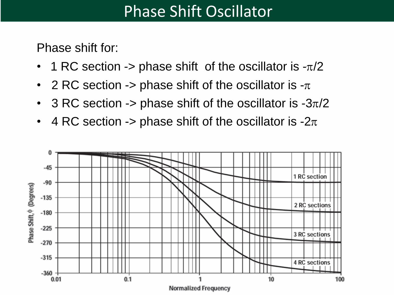
Phase shift for:
• 1 RC section -> phase shift of the oscillator is -/2
• 2 RC section -> phase shift of the oscillator is -
• 3 RC section -> phase shift of the oscillator is -3/2
• 4 RC section -> phase shift of the oscillator is -2

Single Amplifier Phase Shift Oscillator
• It is less distortion from Wien-Bridge. This occurs when output
distortion is very low e.g. -0.46 %, although this design is less
popular these days.
• The three RC sections are cascaded to get the steep slope
between phase and resonant frequency. With three RC
sections, the angle for each section is -/3.
𝜔 = 2𝜋𝑓 =1.732
𝑅𝐶(e. g. tan 60° = 1.732)
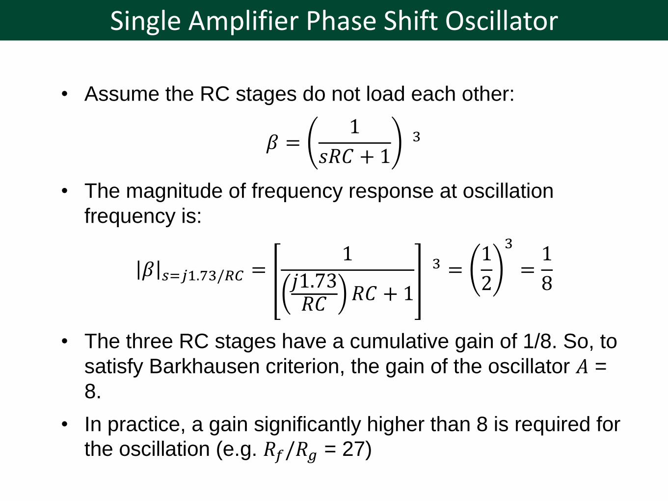
Single Amplifier Phase Shift Oscillator
• Assume the RC stages do not load each other:
𝛽 =1
𝑠𝑅𝐶 + 13
• The magnitude of frequency response at oscillation
frequency is:
𝛽 𝑠=𝑗1.73/𝑅𝐶 =1
𝑗1.73𝑅𝐶
𝑅𝐶 + 1
3 =1
2
3
=1
8
• The three RC stages have a cumulative gain of 1/8. So, to
satisfy Barkhausen criterion, the gain of the oscillator 𝐴 =
8.
• In practice, a gain significantly higher than 8 is required for
the oscillation (e.g. 𝑅𝑓/𝑅𝑔 = 27)

Buffered Phase Shift Oscillator
• The loading effects of the RC chain upset the calculation of
oscillation frequency.
• To eliminate the effects -> voltage followers are used to
isolate various RC stages.
• Typically a quad op amp is used, with final stage to buffer 𝑉𝑜𝑢𝑡 before it is passed to load.
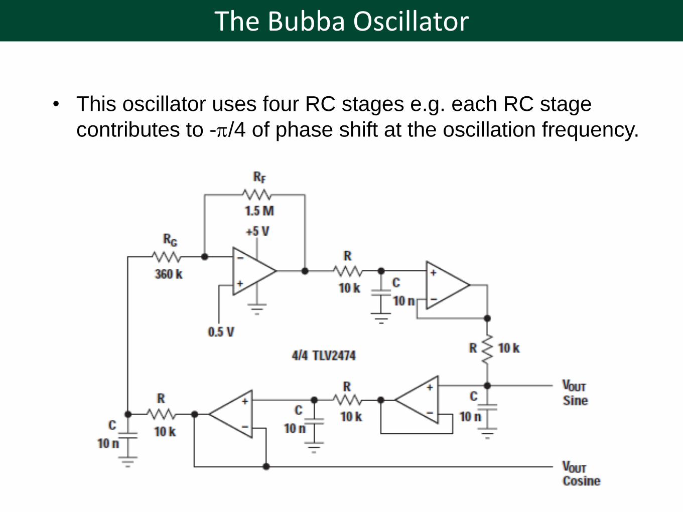
The Bubba Oscillator
• This oscillator uses four RC stages e.g. each RC stage
contributes to -/4 of phase shift at the oscillation frequency.
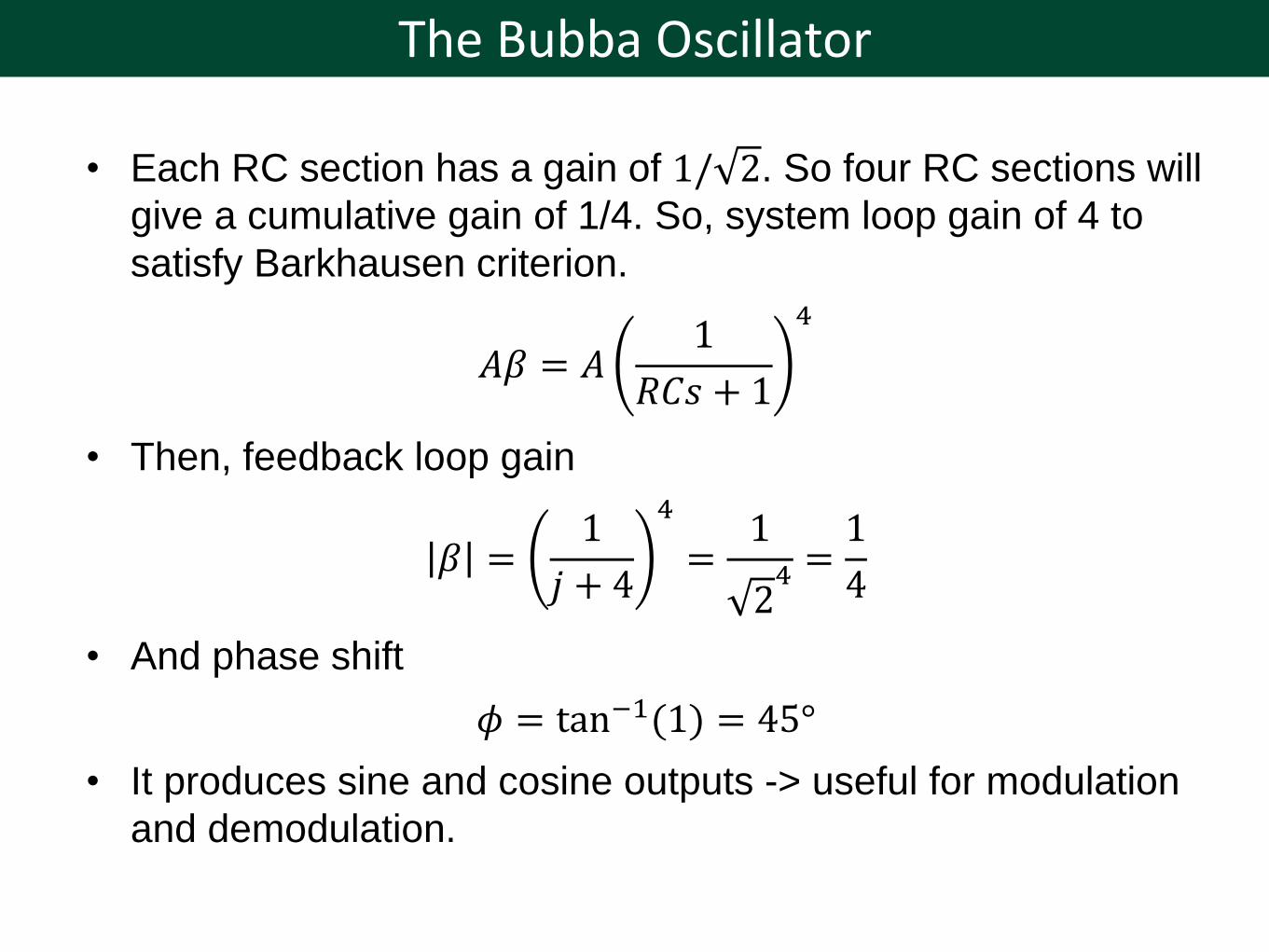
The Bubba Oscillator
• Each RC section has a gain of 1/ 2. So four RC sections will
give a cumulative gain of 1/4. So, system loop gain of 4 to
satisfy Barkhausen criterion.
𝐴𝛽 = 𝐴1
𝑅𝐶𝑠 + 1
4
• Then, feedback loop gain
𝛽 =1
𝑗 + 4
4
=1
24 =
1
4
• And phase shift
𝜙 = tan−1(1) = 45°
• It produces sine and cosine outputs -> useful for modulation
and demodulation.
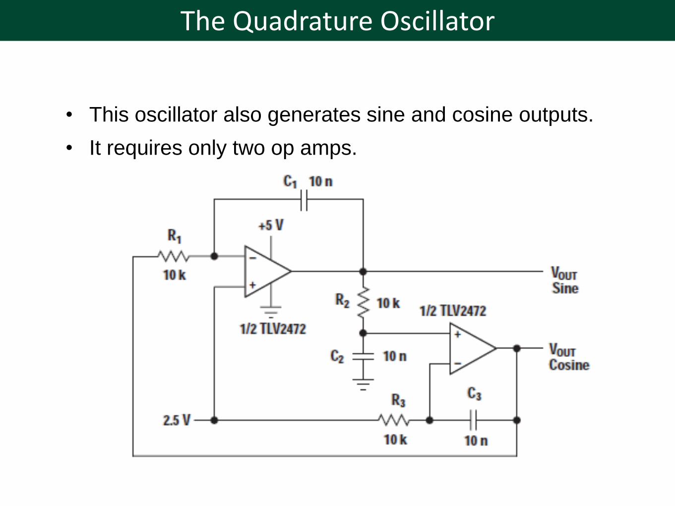
The Quadrature Oscillator
• This oscillator also generates sine and cosine outputs.
• It requires only two op amps.
The Quadrature Oscillator
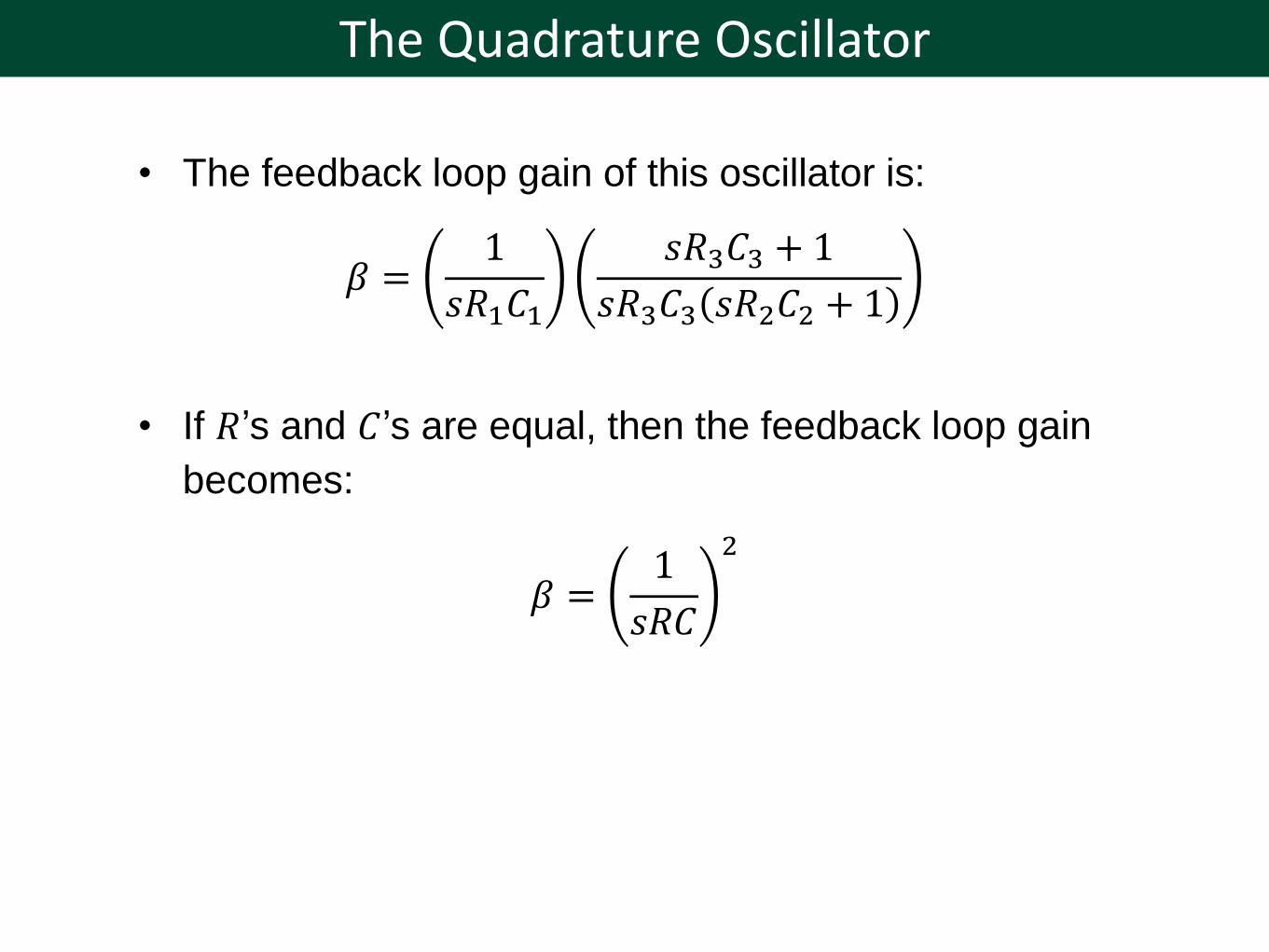
• The feedback loop gain of this oscillator is:
𝛽 =1
𝑠𝑅1𝐶1
𝑠𝑅3𝐶3 + 1
𝑠𝑅3𝐶3 𝑠𝑅2𝐶2 + 1
• If 𝑅’s and 𝐶’s are equal, then the feedback loop gain
becomes:
𝛽 =1
𝑠𝑅𝐶
2