Embed Size (px)
Citation preview
One Way Circuits LimitedPrinted Circuit Board Manufacturer
Front End DRC (Design Rule Checks)
Use Left and Right Cursor keys to navigate ESC to quit presentation
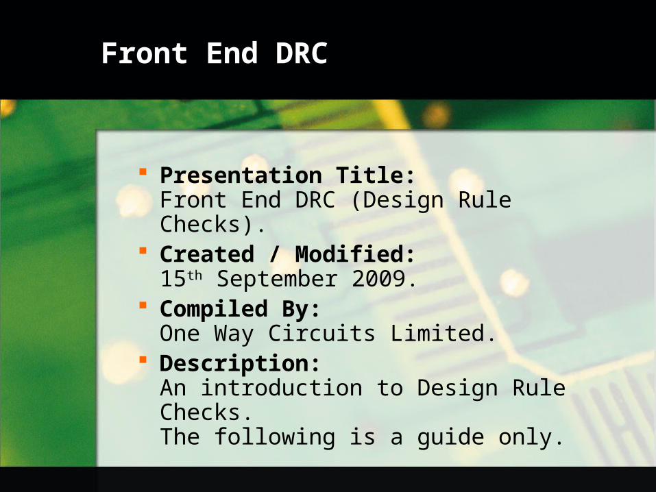
Front End DRC
Presentation Title:Front End DRC (Design Rule Checks).
Created / Modified:15th September 2009.
Compiled By:One Way Circuits Limited.
Description:An introduction to Design Rule Checks.The following is a guide only.
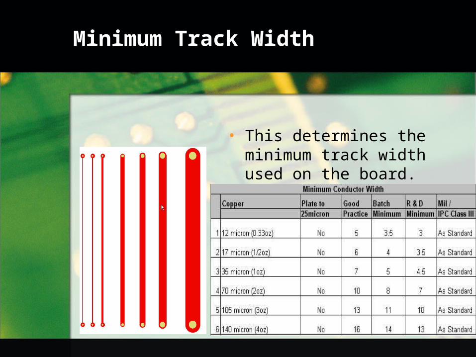
Minimum Track Width
• This determines the minimum track width used on the board.
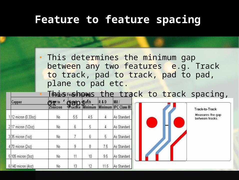
Feature to feature spacing
• This determines the minimum gap between any two features e.g. Track to track, pad to track, pad to pad, plane to pad etc.
• This shows the track to track spacing, or ‘gaps’.
Feature to feature spacing
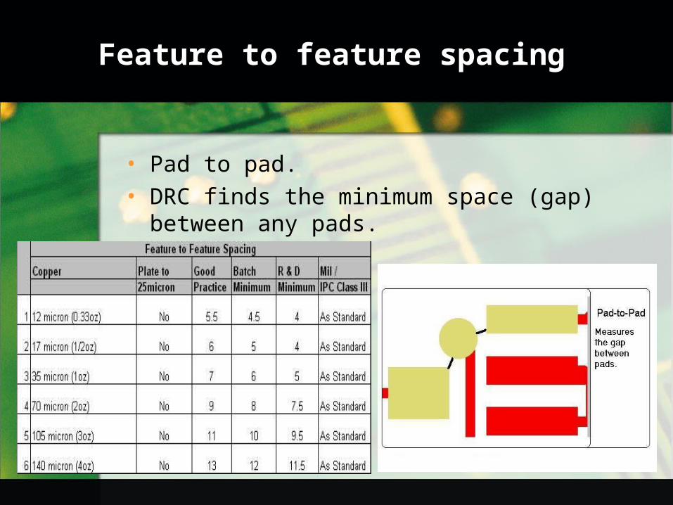
• Pad to pad.• DRC finds the minimum space (gap)
between any pads.
Feature to feature spacing
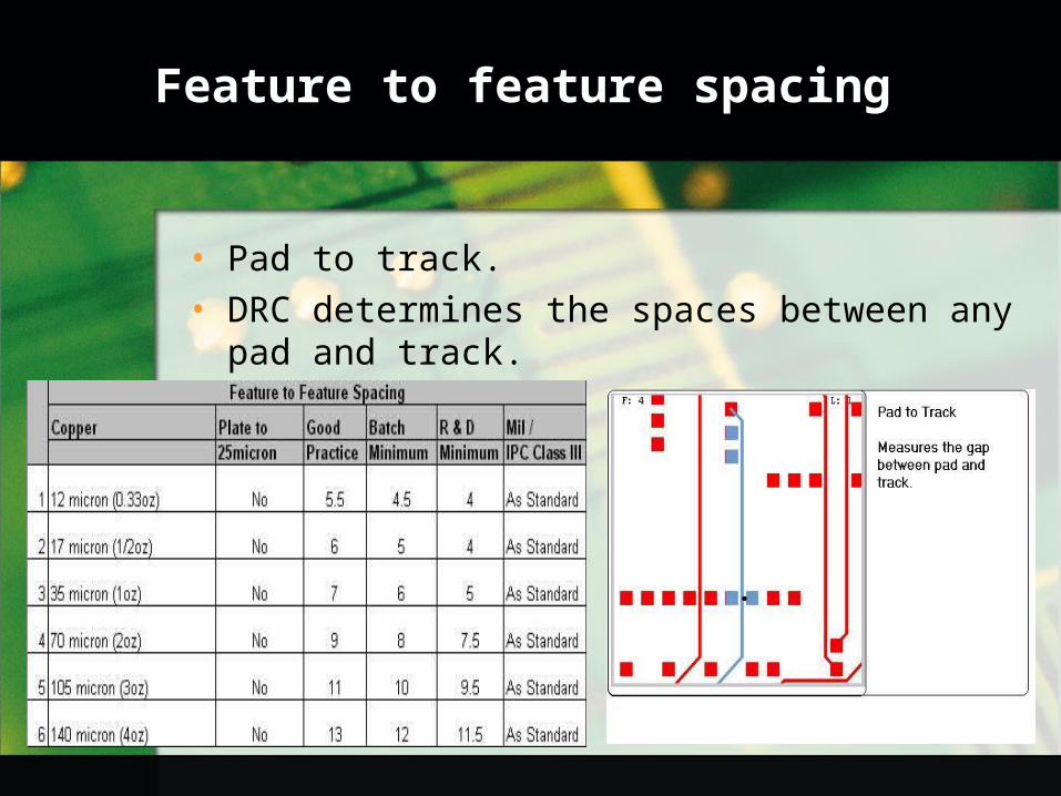
• Pad to track.• DRC determines the spaces between any
pad and track.
Minimum Annular Ring
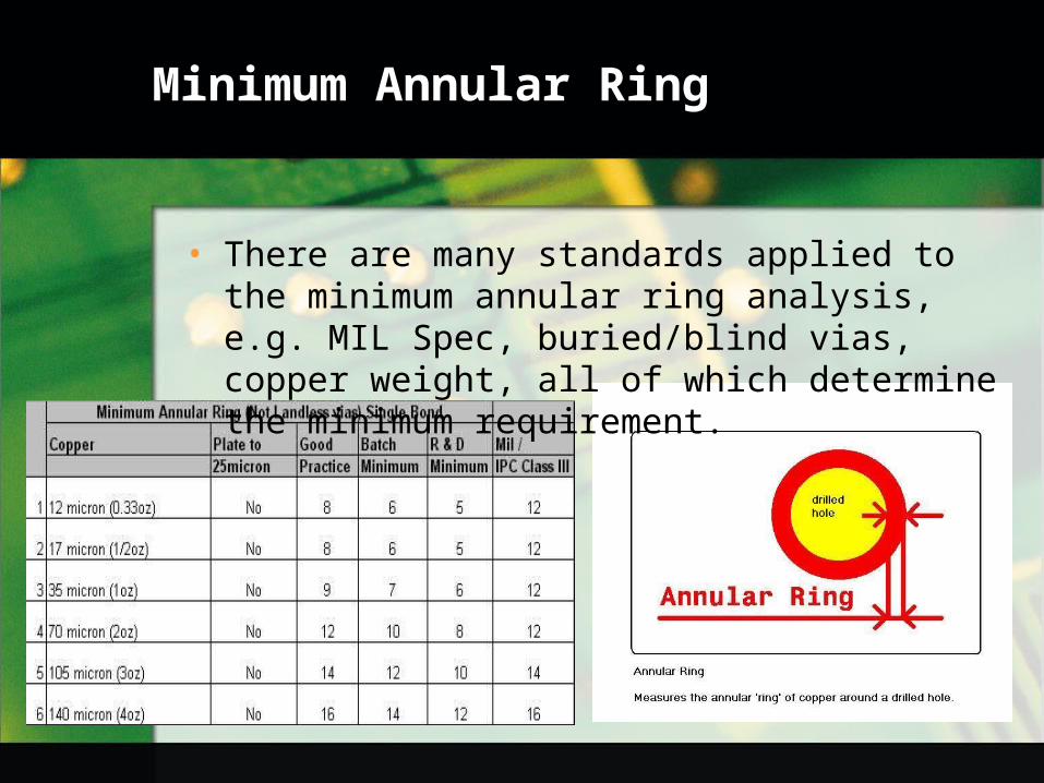
• There are many standards applied to the minimum annular ring analysis, e.g. MIL Spec, buried/blind vias, copper weight, all of which determine the minimum requirement.
Drilled Hole to Feature
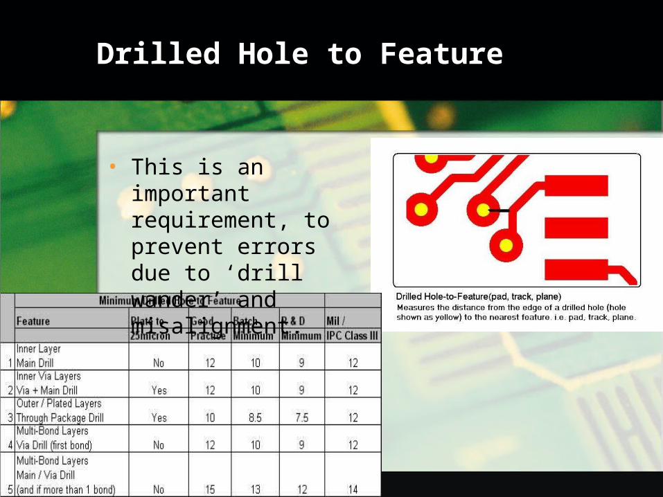
• This is an important requirement, to prevent errors due to ‘drill wander’ and misalignment.
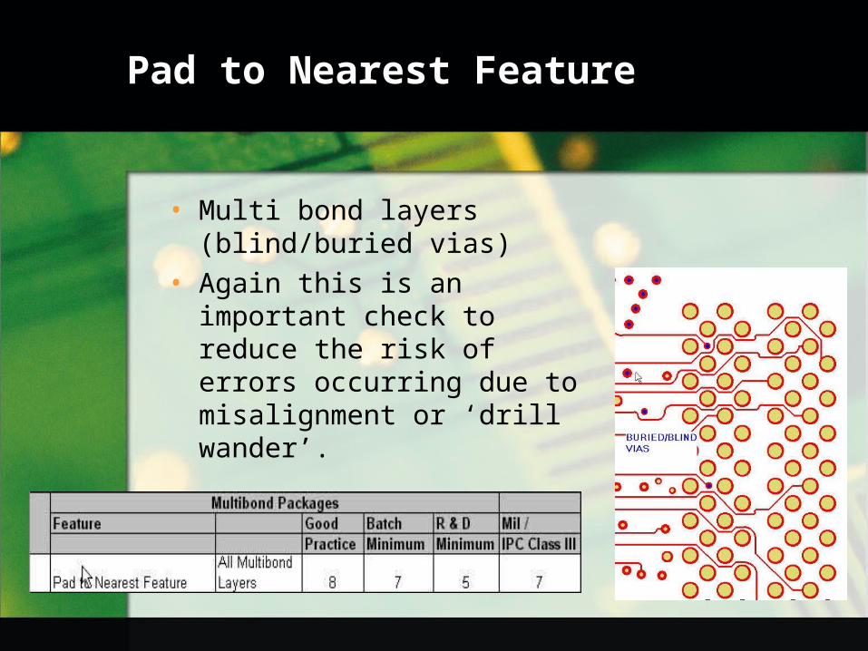
Pad to Nearest Feature
• Multi bond layers (blind/buried vias)
• Again this is an important check to reduce the risk of errors occurring due to misalignment or ‘drill wander’.
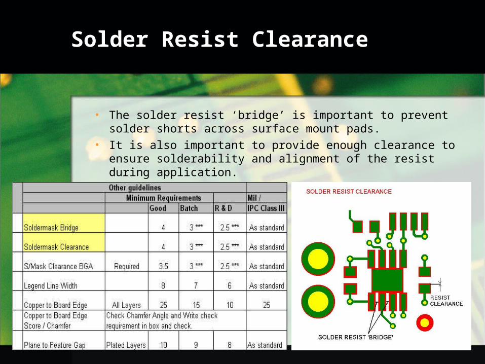
Solder Resist Clearance
• The solder resist ‘bridge’ is important to prevent solder shorts across surface mount pads.
• It is also important to provide enough clearance to ensure solderability and alignment of the resist during application.
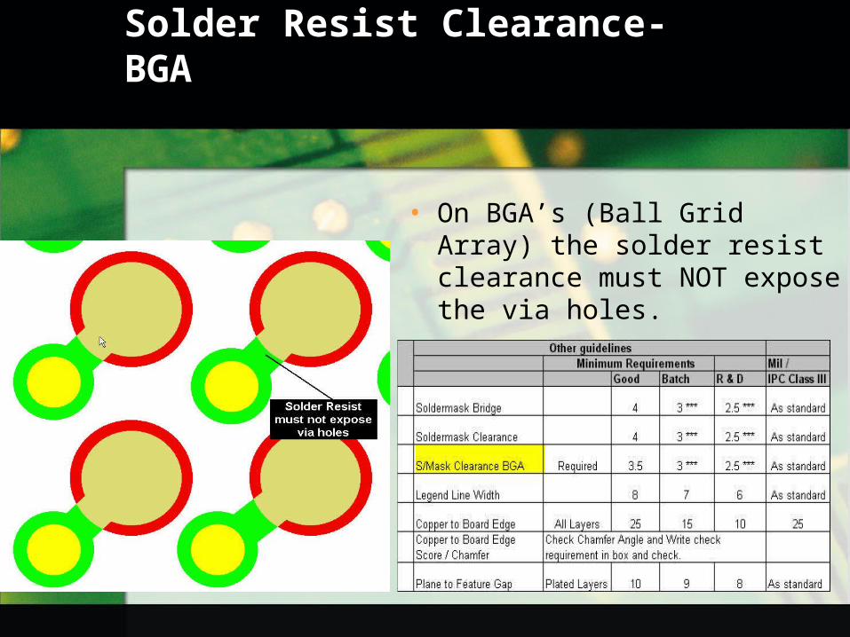
Solder Resist Clearance- BGA
• On BGA’s (Ball Grid Array) the solder resist clearance must NOT expose the via holes.
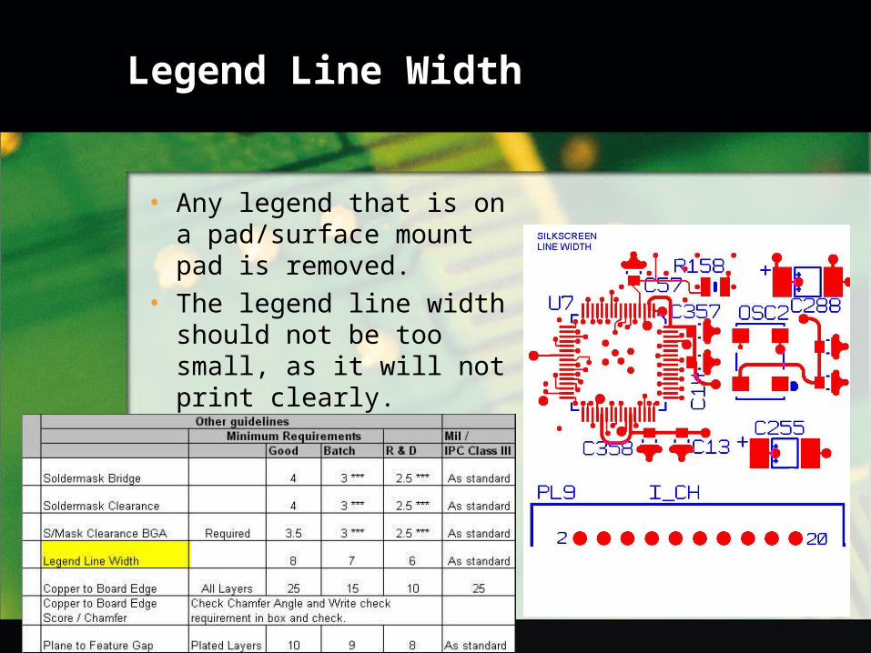
Legend Line Width
• Any legend that is on a pad/surface mount pad is removed.
• The legend line width should not be too small, as it will not print clearly.
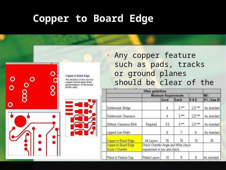
Copper to Board Edge
• Any copper feature such as pads, tracks or ground planes should be clear of the board edge.
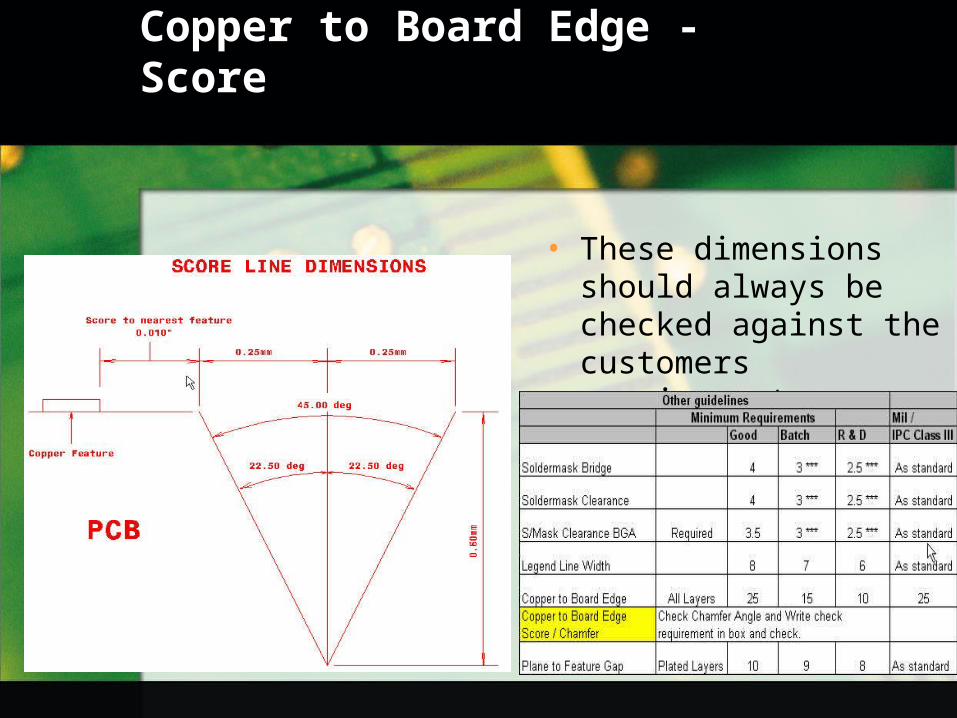
Copper to Board Edge - Score
• These dimensions should always be checked against the customers requirements.
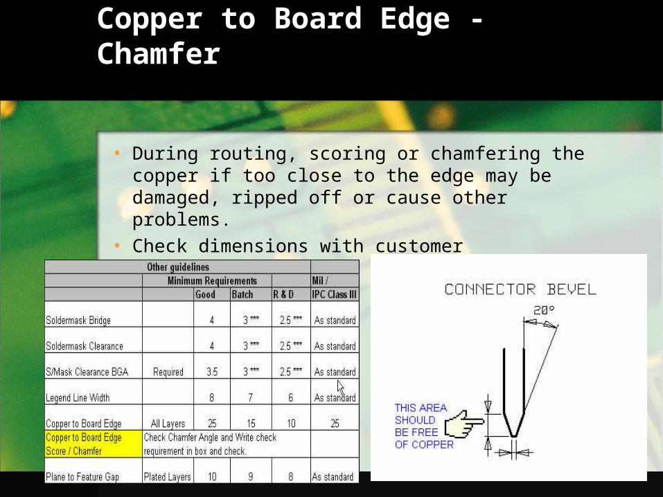
Copper to Board Edge - Chamfer
• During routing, scoring or chamfering the copper if too close to the edge may be damaged, ripped off or cause other problems.
• Check dimensions with customer requirements.
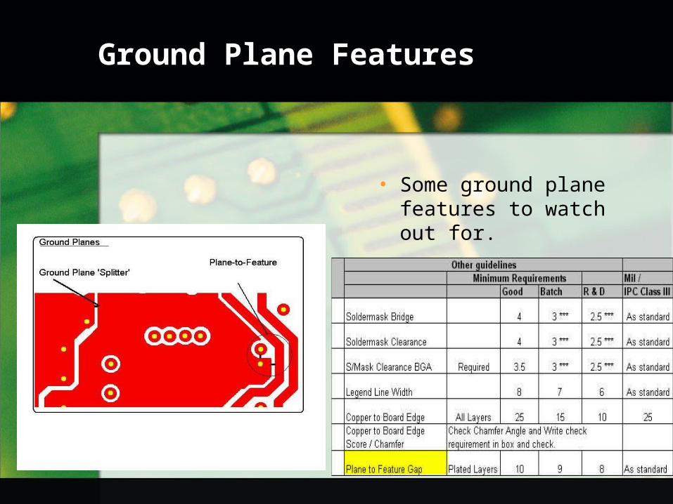
Ground Plane Features
• Some ground plane features to watch out for.
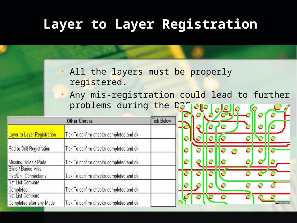
Layer to Layer Registration
• All the layers must be properly registered.• Any mis-registration could lead to further
problems during the DRC.
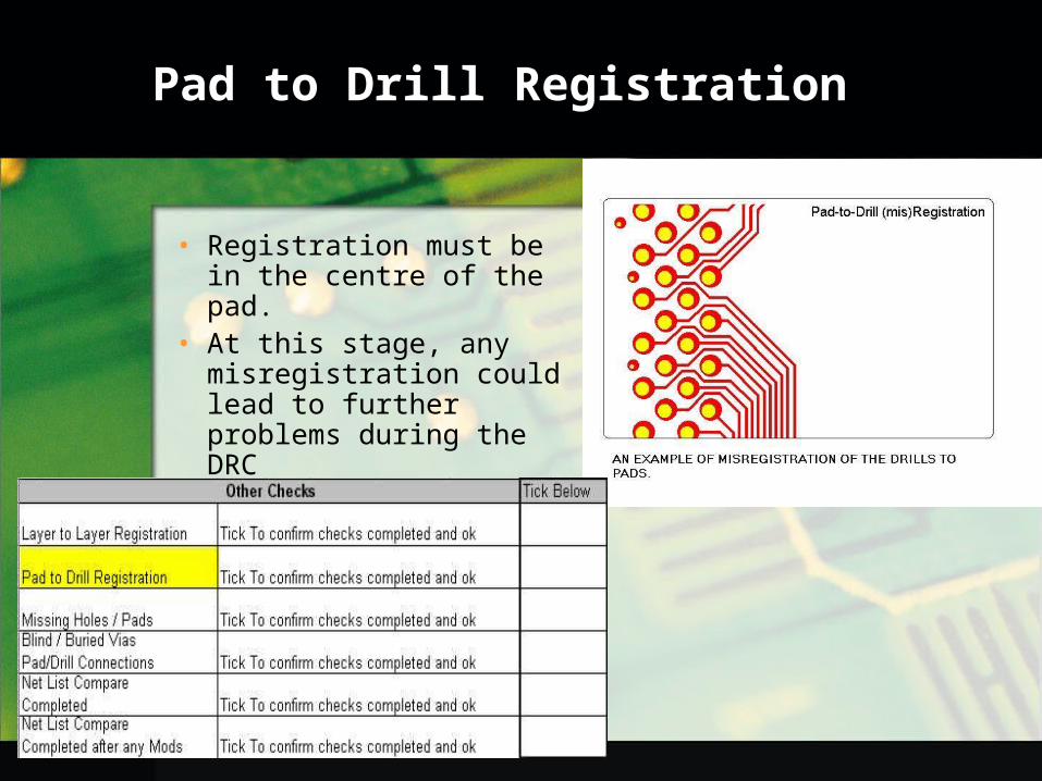
Pad to Drill Registration
• Registration must be in the centre of the pad.
• At this stage, any misregistration could lead to further problems during the DRC
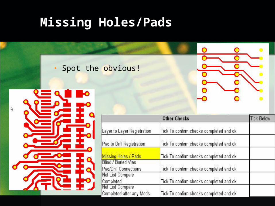
Missing Holes/Pads
• Spot the obvious!
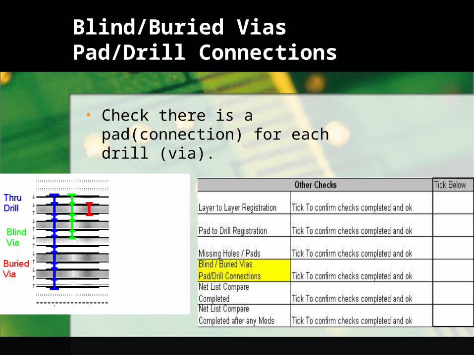
Blind/Buried Vias Pad/Drill Connections
• Check there is a pad(connection) for each drill (via).
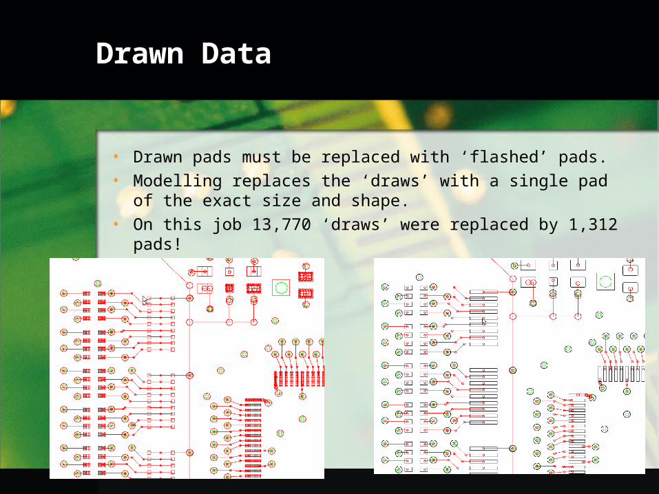
Drawn Data
• Drawn pads must be replaced with ‘flashed’ pads.• Modelling replaces the ‘draws’ with a single pad of the
exact size and shape.• On this job 13,770 ‘draws’ were replaced by 1,312 pads!

Thank you for viewing this presentation