Embed Size (px)
Citation preview
Delivered by Ingenta toUNIVERSITY OF MINNESOTA
IP 128101142152Fri 01 Jun 2012 200048 R
EVIEW
Copyright copy 2012 by American Scientific Publishers
All rights reserved
Printed in the United States of America
Science of Advanced MaterialsVol 4 pp 401ndash406 2012(wwwaspbscomsam)
One-Dimensional Nanostructures byPulsed Laser AblationRusen Yang
Department of Mechanical Engineering University of Minnesota Minneapolis MN 55455
ABSTRACT
One-dimensional (1D) nanostructures represent a unique system for investigating phenomena at the nanoscaleand are also expected to play a critical role as both interconnects and functional components in the fabricationof nanoscale electronic devices Pulsed laser can provide extremely intense energy in a small spot and it canablate virtually any materials Various nanostructures have been investigated and fabricated with pulsed laserablation and this technique is not limited by the type of materials or crystal structures This article focuseson 1D nanostructures and presents an overview of the common growth mechanism of nanowires by pulsedlaser ablation We first introduce a general scheme of the pulsed laser ablation in a tube furnace for thenanowire growth Subsequently we discuss various growth mechanisms involved to generate 1D nanostructuresfrom pulsed laser ablation including vaporndashliquidndashsolid growth oxide-assisted growth and vaporndashsolid growthDefects can also play an important role and they have been observed in the nanowires from different growthprocess
KEYWORDS Laser Ablation Nanostructure Nanowire VLS VS
CONTENTS
1 Introduction 4012 Pulsed Laser Ablation Process 4013 Growth Mechanisms of Nanowires 402
31 VaporndashLiquidndashSolid Process 40232 Oxide-Assistant Growth Process 40433 Vapor-Solid Growth 404
4 Summary 405Acknowledgments 405References and Notes 405
1 INTRODUCTION
One-dimensional (1D) semiconductor nanostructures areof particular interest because of their unique role for thefundamental study as well as their potential applications innanoscale electronic and optoelectronic devices To datevarious new techniques have been developed to grow 1Dnanostructures such as thermal chemical vapor deposition(CVD)1 molecular beam epitaxy (MBE)2 and chemicalbeam epitaxy (CBE)3 Among various techniques to syn-thesize nanomaterials the laser ablation of solid targetsis of particular interest because bulk-quantity nanowirescan be readily obtained directly from solid source mate-rials and this growth method is applicable in synthesizingnanowires containing complex chemical compositions
Email yangrmeumneduReceived 28 April 2011Accepted 19 May 2011
Since Theodore Maiman made the first ruby laser in19604 pulsed laser ablation (PLA) was soon developedand attracted wide interests because of its great potentialin material processing Pulsed laser was firstly employedfor the preparation of thin films in 19655 and then for holepiercing micro-and nanomachining and surface cleaning6
In the past decade PLA has been intensively investigatedfor the synthesis of nanostructures The nanomaterial syn-thesis with PLA can take place in two distinct conditionsone occurs in a vacuum or gaseous environment and theother occurs in liquid The nanomaterials from the solutionnormally have spherical or roughly spherical shape exceptwhen particles aggregate into fractal structure Sphericalor roughly spherical nanomaterials have been the majormaterials from the vacuum or diluted gas Interestingly 1Dnanostructures have also been discovered from laser abla-tion of solid materials in gaseous environment Consider-ing the unique property and application brought by thoseone-dimensional nanostructures we will discuss differentgrowth processes of 1D materials with PLA techniqueStarting with a general description of the PLA method wewill discuss respectively the vaporndashliquidndashsolid (VLS) pro-cess oxide-assistant growth (OAG) and vaporndashsolid (VS)growth and finally conclude with a summary
2 PULSED LASER ABLATION PROCESS
The laser ablation of solid targets is an effective techniqueto produce bulk-quantity nanomaterials directly from the
Sci Adv Mater 2012 Vol 4 No 34 1947-293520124401006 doi101166sam20121296 401
Delivered by Ingenta toUNIVERSITY OF MINNESOTA
IP 128101142152Fri 01 Jun 2012 200048
One-Dimensional Nanostructures by Pulsed Laser Ablation YangREVIEW
solid source materials and it has been employed for thesynthesis of nanostructures such as fullerenes7 and car-bon nanotubes8 Pulsed laser can achieve extremely hightemperature within extremely short time and it has manyadvantages in fabricating nanostructures First due to thehighly intense energy of the laser spot almost any mate-rial can be ablated for the synthesis purpose In additionPLA can generally allow better control over stoichiometryof the deposited materials which will benefit the growthof complex materials Introducing the pulsed laser into thetube furnace has enabled the growth of many high-qualitynanomaterials which cannot be easily achieved otherwiseNanomaterials can be synthesized with ultra-short
(picosecond or femtosecond) pulse910 nanosecondpulse1112 or even continuous-wave conditions1314
although the ablation process is very complicated andcan be different When the laser is focused on the solidtarget the intense laser radiation can cause the mate-rials ejection and plasma plume from the solid targetThe plasma plume will eventually condense to form thinfilm or nanostructures The generation transformation andcondensation of the plasma plume play important rolesin nanomaterials preparation The nanomaterial growth isdetermined by both laser parameters (wavelength pulselength and fluence) and properties of the ambient mediumthat can be controlled with the furnaceWhen the pulse is ultra-short the laser energy is mainly
transferred to the target instantaneously and the plasmaforms right after the laser pulse The plasma will expandswithout any further heating process and condense witha short life Otherwise the later part of the incidentlaser pulse continuously irradiates the plasma plume andenhances the excitation and ionization of the species inthe plume Meanwhile it also irradiates the solid targetto ablate more species into the plume Consequently theplume can expand further with a longer life The interfacebetween the ejected plasma plume and the ambient gasprovides a path for possible chemical reactions and heatexchange Plasma will cool down and condense resultingin the nanostructures either on a substrate or in the coolambient gasFigure 1 is a schematic PLA setup for the growth of
nanomaterials in a tube furnace Tube furnace can achieve
Rusen Yang received his PhD degree in Materials Science and Engineering from GeorgiaInstitute of Technology in 2007 where he continued as Post Doctoral Associate He joinedMechanical Engineering at the University of Minnesota-Twin Cities as an assistant professorin 2010 He has discovered novel nanostructures such as ZnO SnO2 Zn3P2 and investigatedtheir application potentials His most recent work on energy harvester based on piezoelectricnanomaterials made significant contribution in the field of renewable energy
well control over the growth temperature at the substrateflowing gas type and speed and pressure during the wholegrowth process Furnace by itself can be used to grownanomaterials through a vapor deposition process15 whilepulsed laser is another unique and localized heating sourcewith extremely high temperature within extremely shorttime The integration of PLA with furnace has been widelyemployed to grow different nanomaterials PLA can allowbetter control over stoichiometry of the deposited materi-als which will benefit the growth of complex functionalmaterials The solid target for the laser ablation containsthe material or component materials for the targetingnanowires It can also contain impurity metals as the cat-alyst for the VLS growth The target is normally locatedin the middle of the furnace and a substrate or collectingcolder finer is adjacent to the target Under the laser abla-tion the target material will be vaporized and deposited onthe substrate or colder finger With careful control of theparameters for the laser (pulse energy wavelength etc)and the parameters for the furnace (pressure temperaturecarrier gas etc) researcher can synthesize novel nano-structures with excellent controllability
3 GROWTH MECHANISMSOF NANOWIRES
31 VaporndashLiquidndashSolid Process
Since the VLS growth mechanism was proposed by Wag-ner and Ellis in 1964 for silicon whiskers16 this processhas been widely adopted to explain the growth of nano-structures from different methods The impurity metal isnormally induced intentionally to serve as catalyst in liq-uid state to define and guide the growth of nanowires17
However some source materials can decompose underlaser ablation and form liquid droplets to serve as thecatalyst assisting the growth of nanowire Such VLSgrowth without impurity metal is also called self-catalyticor catalyst-free growth1819 The laser-assisted VLS pro-cess has produced nanowires from elementary materials(Si17 Ge17 and B20) binary materials (In2O3
21 SnO222
ZnO23 SiOx24 Zn3P2
25 GaN26 GaAs27 and MgO28)ternary materials (GaAs06P04 InAs05P05 CdSxSe1minusx
29
402 Sci Adv Mater 4 401ndash406 2012
Delivered by Ingenta toUNIVERSITY OF MINNESOTA
IP 128101142152Fri 01 Jun 2012 200048
Yang One-Dimensional Nanostructures by Pulsed Laser AblationREVIEW
Fig 1 Schematic setup for the nanowire growth in a tube furnace withthe laser ablation of a solid target
and indium-tin-oxide (ITO)1830 and even more complexmaterials31 In addition this process has been used forimpurity-doped nanowire32ndash35 as well as block-by-blocksuperlattice nanowires36
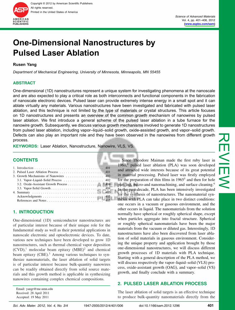
The VLS growth process is schematically shown inFigure 2(a) The target is composed of mainly the sourcematerial for the targeting nanostructure (material Mn in theFig 2) and a small fraction of the catalyst metal (materialMm in the Fig 2) The laser ablation of the target producesthe plasma plume containing mainly Mn with a small frac-tion of Mm The plume quickly cools down and liquiddroplets containing Mm and Mn start to form The supersat-uration due to the continuous addition of Mn into the liquidwill result in the precipitation of Mn and the formation ofthe nanowires as shown in Figure 2(a) The VLS process
Fig 2 Nanowire growth from VLS process (a) Phase diagram usedto guide the selection of metal catalyst and growth temperature(b) Schematic illustration of the nanowire formation from VLS process(c) Bright-field TEM image of single ZnSe nanowire with a Au tip withthe inset showing the [100] zone axis SAED pattern Reprinted with per-mission from [48] Y Jiang et al J Phys Chem B 108 2784 (2004)copy 2004 American Chemical Society
is a widely accepted model for the nanowire growth butthe exact form of vapor species and their interaction withthe catalyst particle require further investigationAlthough the exact role or chemical composition of
vapor species and their interaction with the liquid dropletare not fully understood we can still develop certain guidelines to choose the metal as well as the growth condi-tion The VLS growth method takes advantage of the metalcatalyst in liquid state to initiate and guide the growthof the nanowire Consequently the selection of the metalmaterial and the growth temperature is critical The liquidmetal should be able to dissolve the nanowire componentelement At the same time they cannot react and formmore stable solid phase than the desired nanowire phase Inother words the metal catalyst should be physically activebut chemically stable which also explains that the noblemetal like Au has been successfully used for the growth ofmany nanomaterials In addition the growth condition canalso be estimated with the equilibrium phase diagram forthe elementary material17 or pseudobinary phase diagram37
for more complex materials as shown schematically inFigure 2(b) For instance the phase diagram of Si-Au takesthe form shown in Figure 2(b) with Mn replaced by Siand Mm replaced by Au In comparison the phase diagramfor the binary and ternary materials can be very complexHowever this complexity can be significantly reduced bya pseudobinary phase diagram for the catalyst material andthe targeting nanomaterial For instance the pseudobinaryphase diagram of Au-GaAs exhibit Au-Ga-As liquid aswell as GaAs solid38 which will take a similar form asshown in the Figure 2(b) Both cases exhibit a region withboth the liquid phase and the Mn (Si or GaAs)-rich solidphase Consequently Au can be used for the catalyst togrow Si or GaAs at the proper temperature which is alsoconfirmed experimentally173739 Following the similar pro-cess the metal catalyst as well as the growth temperaturecan be estimated for other nanomaterials with the corre-sponding phase diagramFigure 2(c) shows a ZnSe nanowire terminated with
a Au particle at about 800 C ZnSe vapor generatedby laser ablation was transported by the carrier gas andthen dissolved in the Au film to form nanometer-sizedliquid droplets When the concentration of ZnSe in thedroplet become supersaturated at the substrate tempera-ture ZnSe crystal will precipitate leading to the growthof ZnSe nanowires At the end of the growth the remain-ing droplet solidifies and forms a particle at the tip of thenanowire as shown in Figure 2(c) The selected area elec-tron diffraction (SAED) pattern confirmed the single crys-talline structure of the ZnSe nanowire growing along 001directionWithout introducing impurity metal laser ablation a
(In2O3)09(SnO2)01 target produces droplets with hightin content that initiate the self-catalytically growth ofITO nanowires through the VLS process18 All the ITO
Sci Adv Mater 4 401ndash406 2012 403
Delivered by Ingenta toUNIVERSITY OF MINNESOTA
IP 128101142152Fri 01 Jun 2012 200048
One-Dimensional Nanostructures by Pulsed Laser Ablation YangREVIEW
nanowires are terminated with the solid catalyst which isa common phenomenon for the nanowires from the VLSprocess
32 Oxide-Assistant Growth Process
Itrsquos widely accepted that metal can initiate and guide thegrowth of the nanowires through the VLS process Inaddition oxide has also been shown to assist the growthof nanowires following a so-called oxide-assisted growth(OAG)4041 OAG process is a very versatile method andhas been used to grow nanowires from elemental materials(Si42 Ge)43 binary materials (GaAs11 GaP11 GaN)11 andeven more complex materials (yttriumndashbariumndashcopperndashoxygen YBCO)31
Metal is not necessary for OAG process and no metaldroplet is observed at the tip of the nanowire either Inplace of the metal catalysts oxide materials are purposelyadded to the target with the material of interests Thegrowth of the nanowire can be significantly enhanced bythe oxide For instance mixtures of Si and SiO2
42 GaAsand Ga2O3
44 are used for the growth Si nanowire andGaAs nanowire respectivelyThe OAG process can be discussed with the growth
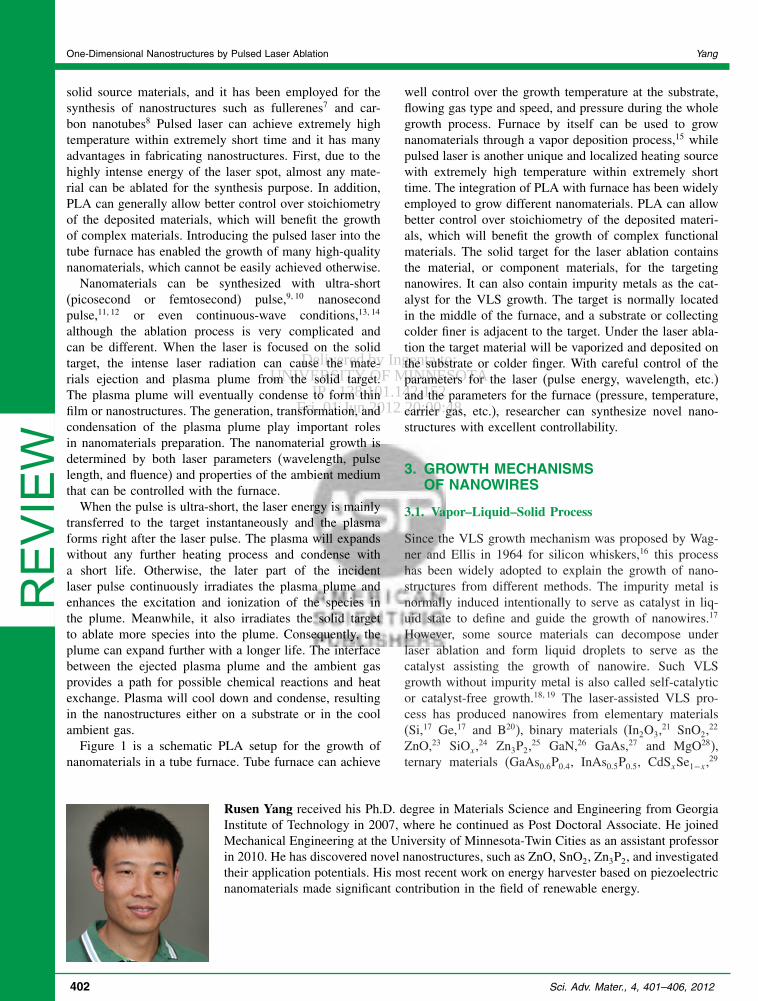
of silicon nanowire as an example45 Silicon oxide in theplasma plume is very important for the nucleation andgrowth of the nanowire The density-functional calcula-tions indicates the energetically favorable configurationsof silicon monoxide clusters (SiO)n for n gt 5 contain asp3 Si core surrounded by a silicon oxide sheath46 Those
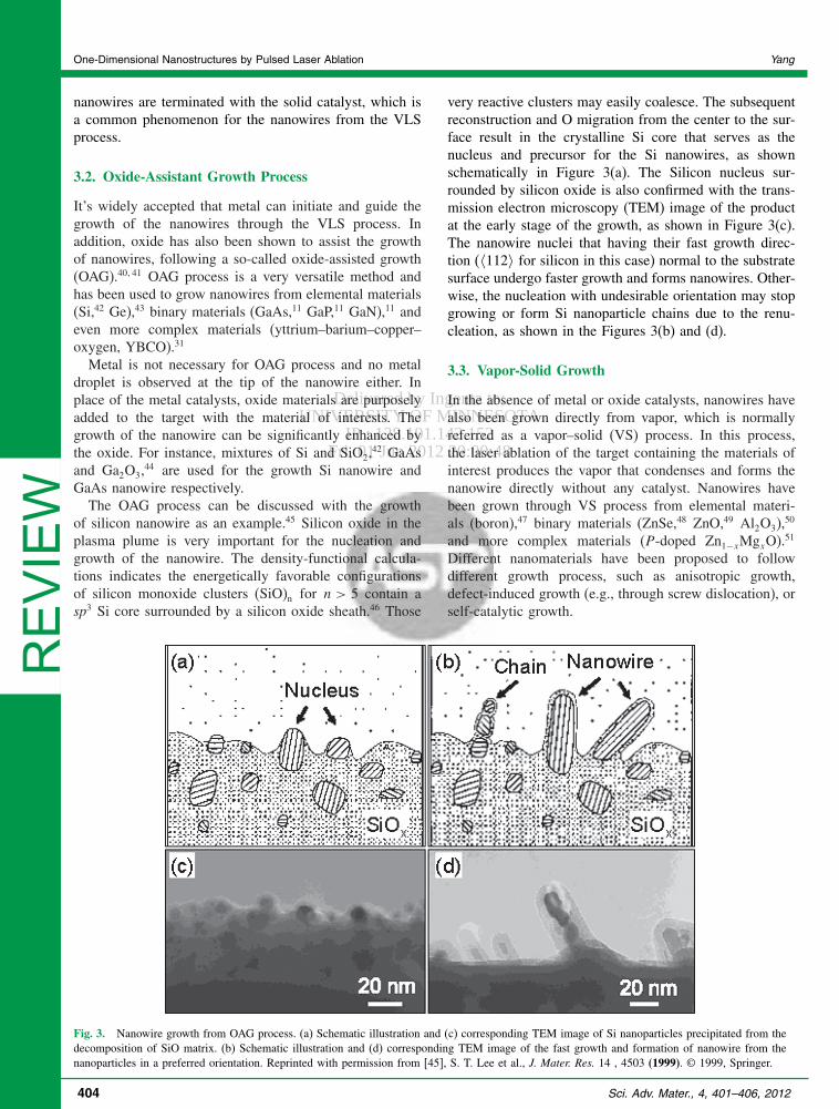
Fig 3 Nanowire growth from OAG process (a) Schematic illustration and (c) corresponding TEM image of Si nanoparticles precipitated from thedecomposition of SiO matrix (b) Schematic illustration and (d) corresponding TEM image of the fast growth and formation of nanowire from thenanoparticles in a preferred orientation Reprinted with permission from [45] S T Lee et al J Mater Res 14 4503 (1999) copy 1999 Springer
very reactive clusters may easily coalesce The subsequentreconstruction and O migration from the center to the sur-face result in the crystalline Si core that serves as thenucleus and precursor for the Si nanowires as shownschematically in Figure 3(a) The Silicon nucleus sur-rounded by silicon oxide is also confirmed with the trans-mission electron microscopy (TEM) image of the productat the early stage of the growth as shown in Figure 3(c)The nanowire nuclei that having their fast growth direc-tion (112 for silicon in this case) normal to the substratesurface undergo faster growth and forms nanowires Other-wise the nucleation with undesirable orientation may stopgrowing or form Si nanoparticle chains due to the renu-cleation as shown in the Figures 3(b) and (d)
33 Vapor-Solid Growth
In the absence of metal or oxide catalysts nanowires havealso been grown directly from vapor which is normallyreferred as a vaporndashsolid (VS) process In this processthe laser ablation of the target containing the materials ofinterest produces the vapor that condenses and forms thenanowire directly without any catalyst Nanowires havebeen grown through VS process from elemental materi-als (boron)47 binary materials (ZnSe48 ZnO49 Al2O3)
50
and more complex materials (P -doped Zn1minusxMgxO)51
Different nanomaterials have been proposed to followdifferent growth process such as anisotropic growthdefect-induced growth (eg through screw dislocation) orself-catalytic growth
404 Sci Adv Mater 4 401ndash406 2012
Delivered by Ingenta toUNIVERSITY OF MINNESOTA
IP 128101142152Fri 01 Jun 2012 200048
Yang One-Dimensional Nanostructures by Pulsed Laser AblationREVIEW
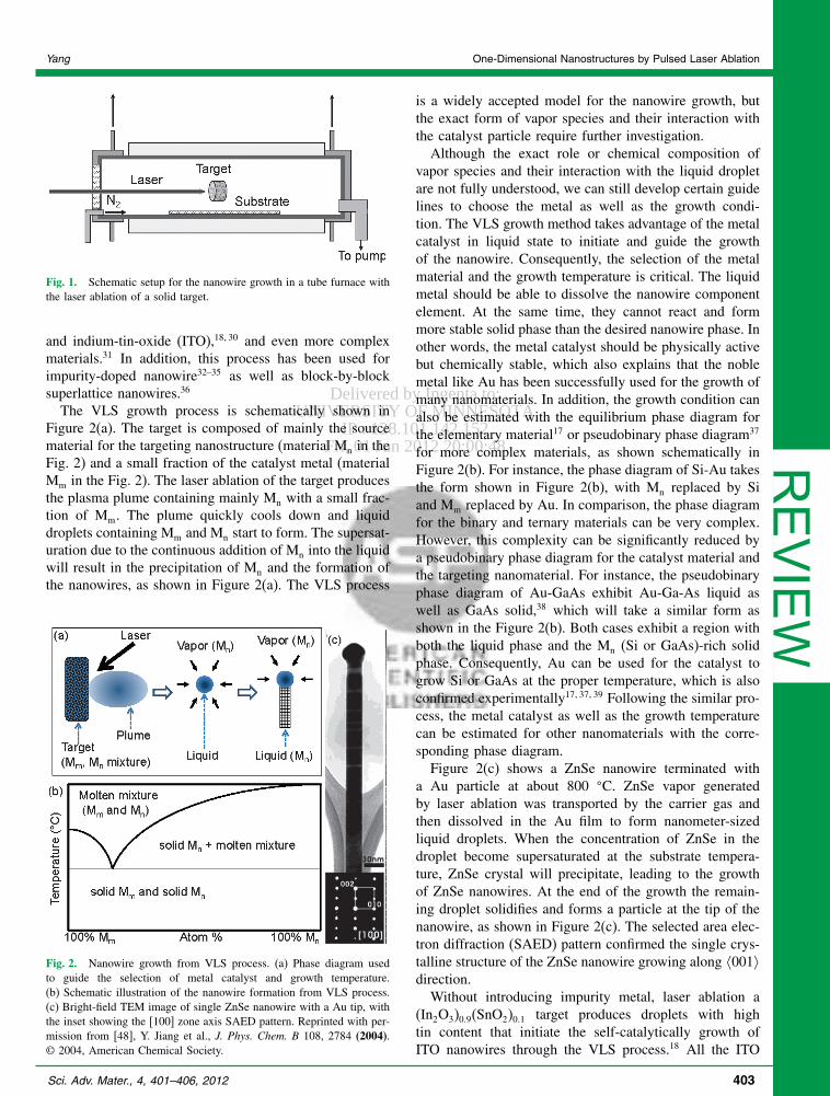
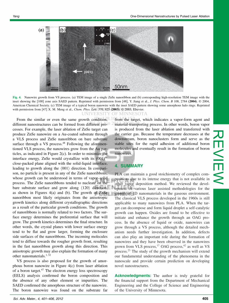
Fig 4 Nanowire growth from VS process (a) TEM image of a single ZnSe nanoribbon and (b) corresponding high-resolution TEM image with theinset showing the [100] zone axis SAED pattern Reprinted with permission from [48] Y Jiang et al J Phys Chem B 108 2784 (2004) copy 2004American Chemical Society (c) TEM image of a typical boron nanowire with the inset SAED pattern showing some amorphous halo rings Reprintedwith permission from [47] X M Meng et al Chem Phys Lett 370 825 (2003) copy 2003 Elsevier
From the similar or even the same growth conditiondifferent nanostructures can be formed from different pro-cesses For example the laser ablation of ZnSe target canproduce ZnSe nanowire on a Au-coated substrate througha VLS process and ZnSe nanoribbon on bare substratesurface through a VS process48 Following the aforemen-tioned VLS process the nanowires grow from the Au par-ticles as indicated in Figure 2(c) In order to minimize theinterface energy ZnSe would crystallize with its (001)48
close-packed plane aligned with the solid-liquid interfaceleading to growth along the 001 direction In compari-son no particle is present in any of the ZnSe nanoribbonswhose growth can be understood in terms of vaporndashsolidprocess The ZnSe nanoribbons tended to nucleate on thebare substrate surface and grow along 120 directionas shown in Figures 4(a) and (b) The growth of ZnSenanoribbon most likely originates from the anisotropicgrowth kinetics along different crystallographic directionsas a result of the particular growth conditions The growthof nanoribbons is normally related to two factors The sur-face energy determines the preferential surface that willgrow The growth kinetics determines the final structure Inother words the crystal planes with lower surface energytend to be flat and grow larger forming the enclosureside surfaces of the nanoribbons The incoming moleculestend to diffuse towards the rougher growth front resultingin the fast nanoribbon growth along this direction Thisanisotropic growth may also explain the formation of manyother nanomaterials152
VS process is also proposed for the growth of amor-phous boron nanowire in Figure 4(c) from laser ablationof a boron target47 The electron energy loss spectroscopy(EELS) analysis confirmed the boron composition andthe absence of any other element or impurities TheSAED confirmed the amorphous structure of the nanowireThe boron nanowire was found on the substrate far
from the target which indicates a vapor-form agent andmaterial-transporting process In other words boron vaporis produced from the laser ablation and transferred withthe carrier gas Because the temperature decreases at thedownstream boron nanoclusters form and serve as thestable sites for the rapid adhesion of additional boronmolecules and eventually result in the formation of boronnanowires
4 SUMMARY
PLA can maintain a good stoichiometry of complex com-positions due to its intense energy that is not available inother vapor deposition method We reviewed the devel-opment of various laser assisted methodologies for thegrowth of 1D nanomaterials in the gaseous environmentThe classical VLS process developed in the 1960s is stillapplicable to many nanowires from PLA When the tar-get can decompose and form liquid droplet a self-catalyticgrowth can happen Oxides are found to be effective toinitiate and enhance the growth through an OAG pro-cess In the absence of liquid or oxide nanowires cangrow through a VS process although the detailed mech-anism needs further investigation In addition defectscan also play an important role during the formation ofnanowires and they have been observed in the nanowiresgrown from VLS process17 OAG process42 as well as VSprocess23 The study of the growth mechanism will extendour fundamental understanding of the phenomena in thenanoscale and provide certain prediction on developingnovel nanostructures
Acknowledgments The author is truly grateful forthe financial support from the Department of MechanicalEngineering and the College of Science and Engineeringof the University of Minnesota
Sci Adv Mater 4 401ndash406 2012 405
Delivered by Ingenta toUNIVERSITY OF MINNESOTA
IP 128101142152Fri 01 Jun 2012 200048
One-Dimensional Nanostructures by Pulsed Laser Ablation YangREVIEW
References and Notes
1 Z W Pan Z R Dai and Z L Wang Science 291 1947 (2001)2 Z H Wu X Y Mei D Kim M Blumin and H E Ruda Appl
Phys Lett 81 5177 (2002)3 M T Bjork B J Ohlsson T Sass A I Persson C Thelander
M H Magnusson K Deppert L R Wallenberg and L SamuelsonAppl Phys Lett 80 1058 (2002)
4 I H Maiman Nature 187 493 (1960)5 H M Smith and A F Turner Appl Optics 4 147 (1965)6 V Kovalenko SPIE-Int Soc Opt Eng 5449 424 (2004)7 H W Kroto J R Heath S C OrsquoBrien R F Curl and R E
Smalley Nature 318 162 (1985)8 A Thess R Lee P Nikolaev H J Dai P Petit J Robert C H Xu
Y H Lee S G Kim A G Rinzler D T Colbert G E ScuseriaD Tomanek J E Fischer and R E Smalley Science 273 483(1996)
9 Y F Zhang R E Russo and S S Mao Appl Phys Lett87 133115 (2005)
10 T Q Jia H X Chen M Huang X J Wu F L Zhao M BabaM Suzuki H Kuroda J R Qiu R X Li and Z Z Xu Appl PhysLett 89 101116 (2006)
11 W S Shi Y F Zheng N Wang C S Lee and S T Lee AdvMater 13 591 (2001)
12 Y Jiang X M Meng J Liu Z R Hong C S Lee and S T LeeAdv Mater 15 1195 (2003)
13 W K Maser E Munoz A M Benito M T Martinez G F de laFuente Y Maniette E Anglaret and J L Sauvajol Chem PhysLett 292 587 (1998)
14 E Munoz W K Maser A M Benito M T Martinez G F de laFuente A Righi J L Sauvajol E Anglaret and Y Maniette ApplPhys a-Mater 70 145 (2000)
15 R S Yang and Z L Wang Philos Mag 87 2097 (2007)16 R S Wagner and W C Ellis Appl Phys Lett 4 89 (1964)17 A M Morales and C M Lieber Science 279 208 (1998)18 R Savu and E Joanni J Mater Sci 43 609 (2008)19 Y Sun G M Fuge and M N R Ashfold Chem Phys Lett 396
21 (2004)20 Y J Zhang H Ago M Yumura S Ohshima K Uchida
T Komatsu and S Iijima Chem Phys Lett 385 177 (2004)21 C Li D H Zhang S Han X L Liu T Tang and C W Zhou
Adv Mater 15 143 (2003)22 Z Q Liu D H Zhang S Han C Li T Tang W Jin X L Liu
B Lei and C W Zhou Adv Mater 15 1754 (2003)23 I Amarilio-Burshtein S Tamir and Y Lifshitz Appl Phys Lett
96 103104 (2010)24 Y Lifshitz I Aharonovich and S Tamir Nanotechnology
19 065608 (2008)25 R S Yang Y L Chueh J R Morber R Snyder L J Chou and
Z L Wang Nano Lett 7 269 (2007)
26 M H Hong D K T Ng L S Tan Y Zhou and G X ChenJ Alloy Compd 449 250 (2008)
27 X W Zhao A J Hauser T R Lemberger and F Y Yang Nan-otechnology 18 485608 (2007)
28 T Yanagida A Marcu K Nagashima H Tanaka and T KawaiJ Appl Phys 102 016102 (2007)
29 Y J Choi I S Hwang J H Park S Nahm and J G Park Nan-otechnology 17 3775 (2006)
30 R Savu and E Joanni Scripta Mater 55 979 (2006)31 Y F Zhang Y H Tang X F Duan Y Zhang C S Lee N Wang
I Bello and S T Lee Chem Phys Lett 323 180 (2000)32 S Y Lee Y W Song and S Lee J Cryst Growth 310 4612
(2008)33 S Y Lee and Y W Song Thin Solid Films 518 1323 (2009)34 S Y Lee Y W Song and K Kim Thin Solid Films 518 1318
(2009)35 B Eisenhawer D Zhang R Clavel A Berger J Michler and
S Christiansen Nanotechnology 22 075706 (2011)36 Y Y Wu R Fan and P D Yang Nano Lett 2 83 (2002)37 X F Duan and C M Lieber Adv Mater 12 298 (2000)38 M B Panish J Electrochem Soc 114 516 (1967)39 M L Taheri B W Reed T B LaGrange and N D Browning
Small 4 2187 (2008)40 S T Lee N Wang Y F Zhang and Y H Tang Mrs Bull 24 36
(1999)41 R Q Zhang Y Lifshitz and S T Lee Adv Mater 15 635
(2003)42 N Wang Y F Zhang Y H Tang C S Lee and S T Lee Appl
Phys Lett 73 3902 (1998)43 Y F Zhang Y H Tang N Wang C S Lee I Bello and S T
Lee Phys Rev B 61 4518 (2000)44 W S Shi Y F Zheng N Wang C S Lee and S T Lee Appl
Phys Lett 78 3304 (2001)45 S T Lee Y F Zhang N Wang Y H Tang I Bello C S Lee
and Y W Chung J Mater Res 14 4503 (1999)46 R Q Zhang M W Zhao and S T Lee Phys Rev Lett 93 095503
(2004)47 X M Meng J Q Hu Y Jiang C S Lee and S T Lee Chem
Phys Lett 370 825 (2003)48 Y Jiang X M Meng W C Yiu J Liu J X Ding C S Lee and
S T Lee J Phys Chem B 108 2784 (2004)49 T Okada R Q Guo J Nishimura M Matsumoto and
D Nakamura Appl Phys a-Mater 93 843 (2008)50 J Proost and S Van Boxel J Mater Chem 14 3058
(2004)51 S S Lin J I Hong J H Song Y Zhu H P He Z Xu Y G
Wei Y Ding R L Snyder and Z L Wang Nano Lett 9 3877(2009)
52 Z L Wang Adv Mater 15 432 (2003)
406 Sci Adv Mater 4 401ndash406 2012
Delivered by Ingenta toUNIVERSITY OF MINNESOTA
IP 128101142152Fri 01 Jun 2012 200048
One-Dimensional Nanostructures by Pulsed Laser Ablation YangREVIEW
solid source materials and it has been employed for thesynthesis of nanostructures such as fullerenes7 and car-bon nanotubes8 Pulsed laser can achieve extremely hightemperature within extremely short time and it has manyadvantages in fabricating nanostructures First due to thehighly intense energy of the laser spot almost any mate-rial can be ablated for the synthesis purpose In additionPLA can generally allow better control over stoichiometryof the deposited materials which will benefit the growthof complex materials Introducing the pulsed laser into thetube furnace has enabled the growth of many high-qualitynanomaterials which cannot be easily achieved otherwiseNanomaterials can be synthesized with ultra-short
(picosecond or femtosecond) pulse910 nanosecondpulse1112 or even continuous-wave conditions1314
although the ablation process is very complicated andcan be different When the laser is focused on the solidtarget the intense laser radiation can cause the mate-rials ejection and plasma plume from the solid targetThe plasma plume will eventually condense to form thinfilm or nanostructures The generation transformation andcondensation of the plasma plume play important rolesin nanomaterials preparation The nanomaterial growth isdetermined by both laser parameters (wavelength pulselength and fluence) and properties of the ambient mediumthat can be controlled with the furnaceWhen the pulse is ultra-short the laser energy is mainly
transferred to the target instantaneously and the plasmaforms right after the laser pulse The plasma will expandswithout any further heating process and condense witha short life Otherwise the later part of the incidentlaser pulse continuously irradiates the plasma plume andenhances the excitation and ionization of the species inthe plume Meanwhile it also irradiates the solid targetto ablate more species into the plume Consequently theplume can expand further with a longer life The interfacebetween the ejected plasma plume and the ambient gasprovides a path for possible chemical reactions and heatexchange Plasma will cool down and condense resultingin the nanostructures either on a substrate or in the coolambient gasFigure 1 is a schematic PLA setup for the growth of
nanomaterials in a tube furnace Tube furnace can achieve
Rusen Yang received his PhD degree in Materials Science and Engineering from GeorgiaInstitute of Technology in 2007 where he continued as Post Doctoral Associate He joinedMechanical Engineering at the University of Minnesota-Twin Cities as an assistant professorin 2010 He has discovered novel nanostructures such as ZnO SnO2 Zn3P2 and investigatedtheir application potentials His most recent work on energy harvester based on piezoelectricnanomaterials made significant contribution in the field of renewable energy
well control over the growth temperature at the substrateflowing gas type and speed and pressure during the wholegrowth process Furnace by itself can be used to grownanomaterials through a vapor deposition process15 whilepulsed laser is another unique and localized heating sourcewith extremely high temperature within extremely shorttime The integration of PLA with furnace has been widelyemployed to grow different nanomaterials PLA can allowbetter control over stoichiometry of the deposited materi-als which will benefit the growth of complex functionalmaterials The solid target for the laser ablation containsthe material or component materials for the targetingnanowires It can also contain impurity metals as the cat-alyst for the VLS growth The target is normally locatedin the middle of the furnace and a substrate or collectingcolder finer is adjacent to the target Under the laser abla-tion the target material will be vaporized and deposited onthe substrate or colder finger With careful control of theparameters for the laser (pulse energy wavelength etc)and the parameters for the furnace (pressure temperaturecarrier gas etc) researcher can synthesize novel nano-structures with excellent controllability
3 GROWTH MECHANISMSOF NANOWIRES
31 VaporndashLiquidndashSolid Process
Since the VLS growth mechanism was proposed by Wag-ner and Ellis in 1964 for silicon whiskers16 this processhas been widely adopted to explain the growth of nano-structures from different methods The impurity metal isnormally induced intentionally to serve as catalyst in liq-uid state to define and guide the growth of nanowires17
However some source materials can decompose underlaser ablation and form liquid droplets to serve as thecatalyst assisting the growth of nanowire Such VLSgrowth without impurity metal is also called self-catalyticor catalyst-free growth1819 The laser-assisted VLS pro-cess has produced nanowires from elementary materials(Si17 Ge17 and B20) binary materials (In2O3
21 SnO222
ZnO23 SiOx24 Zn3P2
25 GaN26 GaAs27 and MgO28)ternary materials (GaAs06P04 InAs05P05 CdSxSe1minusx
29
402 Sci Adv Mater 4 401ndash406 2012
Delivered by Ingenta toUNIVERSITY OF MINNESOTA
IP 128101142152Fri 01 Jun 2012 200048
Yang One-Dimensional Nanostructures by Pulsed Laser AblationREVIEW
Fig 1 Schematic setup for the nanowire growth in a tube furnace withthe laser ablation of a solid target
and indium-tin-oxide (ITO)1830 and even more complexmaterials31 In addition this process has been used forimpurity-doped nanowire32ndash35 as well as block-by-blocksuperlattice nanowires36
The VLS growth process is schematically shown inFigure 2(a) The target is composed of mainly the sourcematerial for the targeting nanostructure (material Mn in theFig 2) and a small fraction of the catalyst metal (materialMm in the Fig 2) The laser ablation of the target producesthe plasma plume containing mainly Mn with a small frac-tion of Mm The plume quickly cools down and liquiddroplets containing Mm and Mn start to form The supersat-uration due to the continuous addition of Mn into the liquidwill result in the precipitation of Mn and the formation ofthe nanowires as shown in Figure 2(a) The VLS process
Fig 2 Nanowire growth from VLS process (a) Phase diagram usedto guide the selection of metal catalyst and growth temperature(b) Schematic illustration of the nanowire formation from VLS process(c) Bright-field TEM image of single ZnSe nanowire with a Au tip withthe inset showing the [100] zone axis SAED pattern Reprinted with per-mission from [48] Y Jiang et al J Phys Chem B 108 2784 (2004)copy 2004 American Chemical Society
is a widely accepted model for the nanowire growth butthe exact form of vapor species and their interaction withthe catalyst particle require further investigationAlthough the exact role or chemical composition of
vapor species and their interaction with the liquid dropletare not fully understood we can still develop certain guidelines to choose the metal as well as the growth condi-tion The VLS growth method takes advantage of the metalcatalyst in liquid state to initiate and guide the growthof the nanowire Consequently the selection of the metalmaterial and the growth temperature is critical The liquidmetal should be able to dissolve the nanowire componentelement At the same time they cannot react and formmore stable solid phase than the desired nanowire phase Inother words the metal catalyst should be physically activebut chemically stable which also explains that the noblemetal like Au has been successfully used for the growth ofmany nanomaterials In addition the growth condition canalso be estimated with the equilibrium phase diagram forthe elementary material17 or pseudobinary phase diagram37
for more complex materials as shown schematically inFigure 2(b) For instance the phase diagram of Si-Au takesthe form shown in Figure 2(b) with Mn replaced by Siand Mm replaced by Au In comparison the phase diagramfor the binary and ternary materials can be very complexHowever this complexity can be significantly reduced bya pseudobinary phase diagram for the catalyst material andthe targeting nanomaterial For instance the pseudobinaryphase diagram of Au-GaAs exhibit Au-Ga-As liquid aswell as GaAs solid38 which will take a similar form asshown in the Figure 2(b) Both cases exhibit a region withboth the liquid phase and the Mn (Si or GaAs)-rich solidphase Consequently Au can be used for the catalyst togrow Si or GaAs at the proper temperature which is alsoconfirmed experimentally173739 Following the similar pro-cess the metal catalyst as well as the growth temperaturecan be estimated for other nanomaterials with the corre-sponding phase diagramFigure 2(c) shows a ZnSe nanowire terminated with
a Au particle at about 800 C ZnSe vapor generatedby laser ablation was transported by the carrier gas andthen dissolved in the Au film to form nanometer-sizedliquid droplets When the concentration of ZnSe in thedroplet become supersaturated at the substrate tempera-ture ZnSe crystal will precipitate leading to the growthof ZnSe nanowires At the end of the growth the remain-ing droplet solidifies and forms a particle at the tip of thenanowire as shown in Figure 2(c) The selected area elec-tron diffraction (SAED) pattern confirmed the single crys-talline structure of the ZnSe nanowire growing along 001directionWithout introducing impurity metal laser ablation a
(In2O3)09(SnO2)01 target produces droplets with hightin content that initiate the self-catalytically growth ofITO nanowires through the VLS process18 All the ITO
Sci Adv Mater 4 401ndash406 2012 403
Delivered by Ingenta toUNIVERSITY OF MINNESOTA
IP 128101142152Fri 01 Jun 2012 200048
One-Dimensional Nanostructures by Pulsed Laser Ablation YangREVIEW
nanowires are terminated with the solid catalyst which isa common phenomenon for the nanowires from the VLSprocess
32 Oxide-Assistant Growth Process
Itrsquos widely accepted that metal can initiate and guide thegrowth of the nanowires through the VLS process Inaddition oxide has also been shown to assist the growthof nanowires following a so-called oxide-assisted growth(OAG)4041 OAG process is a very versatile method andhas been used to grow nanowires from elemental materials(Si42 Ge)43 binary materials (GaAs11 GaP11 GaN)11 andeven more complex materials (yttriumndashbariumndashcopperndashoxygen YBCO)31
Metal is not necessary for OAG process and no metaldroplet is observed at the tip of the nanowire either Inplace of the metal catalysts oxide materials are purposelyadded to the target with the material of interests Thegrowth of the nanowire can be significantly enhanced bythe oxide For instance mixtures of Si and SiO2
42 GaAsand Ga2O3
44 are used for the growth Si nanowire andGaAs nanowire respectivelyThe OAG process can be discussed with the growth
of silicon nanowire as an example45 Silicon oxide in theplasma plume is very important for the nucleation andgrowth of the nanowire The density-functional calcula-tions indicates the energetically favorable configurationsof silicon monoxide clusters (SiO)n for n gt 5 contain asp3 Si core surrounded by a silicon oxide sheath46 Those
Fig 3 Nanowire growth from OAG process (a) Schematic illustration and (c) corresponding TEM image of Si nanoparticles precipitated from thedecomposition of SiO matrix (b) Schematic illustration and (d) corresponding TEM image of the fast growth and formation of nanowire from thenanoparticles in a preferred orientation Reprinted with permission from [45] S T Lee et al J Mater Res 14 4503 (1999) copy 1999 Springer
very reactive clusters may easily coalesce The subsequentreconstruction and O migration from the center to the sur-face result in the crystalline Si core that serves as thenucleus and precursor for the Si nanowires as shownschematically in Figure 3(a) The Silicon nucleus sur-rounded by silicon oxide is also confirmed with the trans-mission electron microscopy (TEM) image of the productat the early stage of the growth as shown in Figure 3(c)The nanowire nuclei that having their fast growth direc-tion (112 for silicon in this case) normal to the substratesurface undergo faster growth and forms nanowires Other-wise the nucleation with undesirable orientation may stopgrowing or form Si nanoparticle chains due to the renu-cleation as shown in the Figures 3(b) and (d)
33 Vapor-Solid Growth
In the absence of metal or oxide catalysts nanowires havealso been grown directly from vapor which is normallyreferred as a vaporndashsolid (VS) process In this processthe laser ablation of the target containing the materials ofinterest produces the vapor that condenses and forms thenanowire directly without any catalyst Nanowires havebeen grown through VS process from elemental materi-als (boron)47 binary materials (ZnSe48 ZnO49 Al2O3)
50
and more complex materials (P -doped Zn1minusxMgxO)51
Different nanomaterials have been proposed to followdifferent growth process such as anisotropic growthdefect-induced growth (eg through screw dislocation) orself-catalytic growth
404 Sci Adv Mater 4 401ndash406 2012
Delivered by Ingenta toUNIVERSITY OF MINNESOTA
IP 128101142152Fri 01 Jun 2012 200048
Yang One-Dimensional Nanostructures by Pulsed Laser AblationREVIEW
Fig 4 Nanowire growth from VS process (a) TEM image of a single ZnSe nanoribbon and (b) corresponding high-resolution TEM image with theinset showing the [100] zone axis SAED pattern Reprinted with permission from [48] Y Jiang et al J Phys Chem B 108 2784 (2004) copy 2004American Chemical Society (c) TEM image of a typical boron nanowire with the inset SAED pattern showing some amorphous halo rings Reprintedwith permission from [47] X M Meng et al Chem Phys Lett 370 825 (2003) copy 2003 Elsevier
From the similar or even the same growth conditiondifferent nanostructures can be formed from different pro-cesses For example the laser ablation of ZnSe target canproduce ZnSe nanowire on a Au-coated substrate througha VLS process and ZnSe nanoribbon on bare substratesurface through a VS process48 Following the aforemen-tioned VLS process the nanowires grow from the Au par-ticles as indicated in Figure 2(c) In order to minimize theinterface energy ZnSe would crystallize with its (001)48
close-packed plane aligned with the solid-liquid interfaceleading to growth along the 001 direction In compari-son no particle is present in any of the ZnSe nanoribbonswhose growth can be understood in terms of vaporndashsolidprocess The ZnSe nanoribbons tended to nucleate on thebare substrate surface and grow along 120 directionas shown in Figures 4(a) and (b) The growth of ZnSenanoribbon most likely originates from the anisotropicgrowth kinetics along different crystallographic directionsas a result of the particular growth conditions The growthof nanoribbons is normally related to two factors The sur-face energy determines the preferential surface that willgrow The growth kinetics determines the final structure Inother words the crystal planes with lower surface energytend to be flat and grow larger forming the enclosureside surfaces of the nanoribbons The incoming moleculestend to diffuse towards the rougher growth front resultingin the fast nanoribbon growth along this direction Thisanisotropic growth may also explain the formation of manyother nanomaterials152
VS process is also proposed for the growth of amor-phous boron nanowire in Figure 4(c) from laser ablationof a boron target47 The electron energy loss spectroscopy(EELS) analysis confirmed the boron composition andthe absence of any other element or impurities TheSAED confirmed the amorphous structure of the nanowireThe boron nanowire was found on the substrate far
from the target which indicates a vapor-form agent andmaterial-transporting process In other words boron vaporis produced from the laser ablation and transferred withthe carrier gas Because the temperature decreases at thedownstream boron nanoclusters form and serve as thestable sites for the rapid adhesion of additional boronmolecules and eventually result in the formation of boronnanowires
4 SUMMARY
PLA can maintain a good stoichiometry of complex com-positions due to its intense energy that is not available inother vapor deposition method We reviewed the devel-opment of various laser assisted methodologies for thegrowth of 1D nanomaterials in the gaseous environmentThe classical VLS process developed in the 1960s is stillapplicable to many nanowires from PLA When the tar-get can decompose and form liquid droplet a self-catalyticgrowth can happen Oxides are found to be effective toinitiate and enhance the growth through an OAG pro-cess In the absence of liquid or oxide nanowires cangrow through a VS process although the detailed mech-anism needs further investigation In addition defectscan also play an important role during the formation ofnanowires and they have been observed in the nanowiresgrown from VLS process17 OAG process42 as well as VSprocess23 The study of the growth mechanism will extendour fundamental understanding of the phenomena in thenanoscale and provide certain prediction on developingnovel nanostructures
Acknowledgments The author is truly grateful forthe financial support from the Department of MechanicalEngineering and the College of Science and Engineeringof the University of Minnesota
Sci Adv Mater 4 401ndash406 2012 405
Delivered by Ingenta toUNIVERSITY OF MINNESOTA
IP 128101142152Fri 01 Jun 2012 200048
One-Dimensional Nanostructures by Pulsed Laser Ablation YangREVIEW
References and Notes
1 Z W Pan Z R Dai and Z L Wang Science 291 1947 (2001)2 Z H Wu X Y Mei D Kim M Blumin and H E Ruda Appl
Phys Lett 81 5177 (2002)3 M T Bjork B J Ohlsson T Sass A I Persson C Thelander
M H Magnusson K Deppert L R Wallenberg and L SamuelsonAppl Phys Lett 80 1058 (2002)
4 I H Maiman Nature 187 493 (1960)5 H M Smith and A F Turner Appl Optics 4 147 (1965)6 V Kovalenko SPIE-Int Soc Opt Eng 5449 424 (2004)7 H W Kroto J R Heath S C OrsquoBrien R F Curl and R E
Smalley Nature 318 162 (1985)8 A Thess R Lee P Nikolaev H J Dai P Petit J Robert C H Xu
Y H Lee S G Kim A G Rinzler D T Colbert G E ScuseriaD Tomanek J E Fischer and R E Smalley Science 273 483(1996)
9 Y F Zhang R E Russo and S S Mao Appl Phys Lett87 133115 (2005)
10 T Q Jia H X Chen M Huang X J Wu F L Zhao M BabaM Suzuki H Kuroda J R Qiu R X Li and Z Z Xu Appl PhysLett 89 101116 (2006)
11 W S Shi Y F Zheng N Wang C S Lee and S T Lee AdvMater 13 591 (2001)
12 Y Jiang X M Meng J Liu Z R Hong C S Lee and S T LeeAdv Mater 15 1195 (2003)
13 W K Maser E Munoz A M Benito M T Martinez G F de laFuente Y Maniette E Anglaret and J L Sauvajol Chem PhysLett 292 587 (1998)
14 E Munoz W K Maser A M Benito M T Martinez G F de laFuente A Righi J L Sauvajol E Anglaret and Y Maniette ApplPhys a-Mater 70 145 (2000)
15 R S Yang and Z L Wang Philos Mag 87 2097 (2007)16 R S Wagner and W C Ellis Appl Phys Lett 4 89 (1964)17 A M Morales and C M Lieber Science 279 208 (1998)18 R Savu and E Joanni J Mater Sci 43 609 (2008)19 Y Sun G M Fuge and M N R Ashfold Chem Phys Lett 396
21 (2004)20 Y J Zhang H Ago M Yumura S Ohshima K Uchida
T Komatsu and S Iijima Chem Phys Lett 385 177 (2004)21 C Li D H Zhang S Han X L Liu T Tang and C W Zhou
Adv Mater 15 143 (2003)22 Z Q Liu D H Zhang S Han C Li T Tang W Jin X L Liu
B Lei and C W Zhou Adv Mater 15 1754 (2003)23 I Amarilio-Burshtein S Tamir and Y Lifshitz Appl Phys Lett
96 103104 (2010)24 Y Lifshitz I Aharonovich and S Tamir Nanotechnology
19 065608 (2008)25 R S Yang Y L Chueh J R Morber R Snyder L J Chou and
Z L Wang Nano Lett 7 269 (2007)
26 M H Hong D K T Ng L S Tan Y Zhou and G X ChenJ Alloy Compd 449 250 (2008)
27 X W Zhao A J Hauser T R Lemberger and F Y Yang Nan-otechnology 18 485608 (2007)
28 T Yanagida A Marcu K Nagashima H Tanaka and T KawaiJ Appl Phys 102 016102 (2007)
29 Y J Choi I S Hwang J H Park S Nahm and J G Park Nan-otechnology 17 3775 (2006)
30 R Savu and E Joanni Scripta Mater 55 979 (2006)31 Y F Zhang Y H Tang X F Duan Y Zhang C S Lee N Wang
I Bello and S T Lee Chem Phys Lett 323 180 (2000)32 S Y Lee Y W Song and S Lee J Cryst Growth 310 4612
(2008)33 S Y Lee and Y W Song Thin Solid Films 518 1323 (2009)34 S Y Lee Y W Song and K Kim Thin Solid Films 518 1318
(2009)35 B Eisenhawer D Zhang R Clavel A Berger J Michler and
S Christiansen Nanotechnology 22 075706 (2011)36 Y Y Wu R Fan and P D Yang Nano Lett 2 83 (2002)37 X F Duan and C M Lieber Adv Mater 12 298 (2000)38 M B Panish J Electrochem Soc 114 516 (1967)39 M L Taheri B W Reed T B LaGrange and N D Browning
Small 4 2187 (2008)40 S T Lee N Wang Y F Zhang and Y H Tang Mrs Bull 24 36
(1999)41 R Q Zhang Y Lifshitz and S T Lee Adv Mater 15 635
(2003)42 N Wang Y F Zhang Y H Tang C S Lee and S T Lee Appl
Phys Lett 73 3902 (1998)43 Y F Zhang Y H Tang N Wang C S Lee I Bello and S T
Lee Phys Rev B 61 4518 (2000)44 W S Shi Y F Zheng N Wang C S Lee and S T Lee Appl
Phys Lett 78 3304 (2001)45 S T Lee Y F Zhang N Wang Y H Tang I Bello C S Lee
and Y W Chung J Mater Res 14 4503 (1999)46 R Q Zhang M W Zhao and S T Lee Phys Rev Lett 93 095503
(2004)47 X M Meng J Q Hu Y Jiang C S Lee and S T Lee Chem
Phys Lett 370 825 (2003)48 Y Jiang X M Meng W C Yiu J Liu J X Ding C S Lee and
S T Lee J Phys Chem B 108 2784 (2004)49 T Okada R Q Guo J Nishimura M Matsumoto and
D Nakamura Appl Phys a-Mater 93 843 (2008)50 J Proost and S Van Boxel J Mater Chem 14 3058
(2004)51 S S Lin J I Hong J H Song Y Zhu H P He Z Xu Y G
Wei Y Ding R L Snyder and Z L Wang Nano Lett 9 3877(2009)
52 Z L Wang Adv Mater 15 432 (2003)
406 Sci Adv Mater 4 401ndash406 2012
Delivered by Ingenta toUNIVERSITY OF MINNESOTA
IP 128101142152Fri 01 Jun 2012 200048
Yang One-Dimensional Nanostructures by Pulsed Laser AblationREVIEW
Fig 1 Schematic setup for the nanowire growth in a tube furnace withthe laser ablation of a solid target
and indium-tin-oxide (ITO)1830 and even more complexmaterials31 In addition this process has been used forimpurity-doped nanowire32ndash35 as well as block-by-blocksuperlattice nanowires36
The VLS growth process is schematically shown inFigure 2(a) The target is composed of mainly the sourcematerial for the targeting nanostructure (material Mn in theFig 2) and a small fraction of the catalyst metal (materialMm in the Fig 2) The laser ablation of the target producesthe plasma plume containing mainly Mn with a small frac-tion of Mm The plume quickly cools down and liquiddroplets containing Mm and Mn start to form The supersat-uration due to the continuous addition of Mn into the liquidwill result in the precipitation of Mn and the formation ofthe nanowires as shown in Figure 2(a) The VLS process
Fig 2 Nanowire growth from VLS process (a) Phase diagram usedto guide the selection of metal catalyst and growth temperature(b) Schematic illustration of the nanowire formation from VLS process(c) Bright-field TEM image of single ZnSe nanowire with a Au tip withthe inset showing the [100] zone axis SAED pattern Reprinted with per-mission from [48] Y Jiang et al J Phys Chem B 108 2784 (2004)copy 2004 American Chemical Society
is a widely accepted model for the nanowire growth butthe exact form of vapor species and their interaction withthe catalyst particle require further investigationAlthough the exact role or chemical composition of
vapor species and their interaction with the liquid dropletare not fully understood we can still develop certain guidelines to choose the metal as well as the growth condi-tion The VLS growth method takes advantage of the metalcatalyst in liquid state to initiate and guide the growthof the nanowire Consequently the selection of the metalmaterial and the growth temperature is critical The liquidmetal should be able to dissolve the nanowire componentelement At the same time they cannot react and formmore stable solid phase than the desired nanowire phase Inother words the metal catalyst should be physically activebut chemically stable which also explains that the noblemetal like Au has been successfully used for the growth ofmany nanomaterials In addition the growth condition canalso be estimated with the equilibrium phase diagram forthe elementary material17 or pseudobinary phase diagram37
for more complex materials as shown schematically inFigure 2(b) For instance the phase diagram of Si-Au takesthe form shown in Figure 2(b) with Mn replaced by Siand Mm replaced by Au In comparison the phase diagramfor the binary and ternary materials can be very complexHowever this complexity can be significantly reduced bya pseudobinary phase diagram for the catalyst material andthe targeting nanomaterial For instance the pseudobinaryphase diagram of Au-GaAs exhibit Au-Ga-As liquid aswell as GaAs solid38 which will take a similar form asshown in the Figure 2(b) Both cases exhibit a region withboth the liquid phase and the Mn (Si or GaAs)-rich solidphase Consequently Au can be used for the catalyst togrow Si or GaAs at the proper temperature which is alsoconfirmed experimentally173739 Following the similar pro-cess the metal catalyst as well as the growth temperaturecan be estimated for other nanomaterials with the corre-sponding phase diagramFigure 2(c) shows a ZnSe nanowire terminated with
a Au particle at about 800 C ZnSe vapor generatedby laser ablation was transported by the carrier gas andthen dissolved in the Au film to form nanometer-sizedliquid droplets When the concentration of ZnSe in thedroplet become supersaturated at the substrate tempera-ture ZnSe crystal will precipitate leading to the growthof ZnSe nanowires At the end of the growth the remain-ing droplet solidifies and forms a particle at the tip of thenanowire as shown in Figure 2(c) The selected area elec-tron diffraction (SAED) pattern confirmed the single crys-talline structure of the ZnSe nanowire growing along 001directionWithout introducing impurity metal laser ablation a
(In2O3)09(SnO2)01 target produces droplets with hightin content that initiate the self-catalytically growth ofITO nanowires through the VLS process18 All the ITO
Sci Adv Mater 4 401ndash406 2012 403
Delivered by Ingenta toUNIVERSITY OF MINNESOTA
IP 128101142152Fri 01 Jun 2012 200048
One-Dimensional Nanostructures by Pulsed Laser Ablation YangREVIEW
nanowires are terminated with the solid catalyst which isa common phenomenon for the nanowires from the VLSprocess
32 Oxide-Assistant Growth Process
Itrsquos widely accepted that metal can initiate and guide thegrowth of the nanowires through the VLS process Inaddition oxide has also been shown to assist the growthof nanowires following a so-called oxide-assisted growth(OAG)4041 OAG process is a very versatile method andhas been used to grow nanowires from elemental materials(Si42 Ge)43 binary materials (GaAs11 GaP11 GaN)11 andeven more complex materials (yttriumndashbariumndashcopperndashoxygen YBCO)31
Metal is not necessary for OAG process and no metaldroplet is observed at the tip of the nanowire either Inplace of the metal catalysts oxide materials are purposelyadded to the target with the material of interests Thegrowth of the nanowire can be significantly enhanced bythe oxide For instance mixtures of Si and SiO2
42 GaAsand Ga2O3
44 are used for the growth Si nanowire andGaAs nanowire respectivelyThe OAG process can be discussed with the growth
of silicon nanowire as an example45 Silicon oxide in theplasma plume is very important for the nucleation andgrowth of the nanowire The density-functional calcula-tions indicates the energetically favorable configurationsof silicon monoxide clusters (SiO)n for n gt 5 contain asp3 Si core surrounded by a silicon oxide sheath46 Those
Fig 3 Nanowire growth from OAG process (a) Schematic illustration and (c) corresponding TEM image of Si nanoparticles precipitated from thedecomposition of SiO matrix (b) Schematic illustration and (d) corresponding TEM image of the fast growth and formation of nanowire from thenanoparticles in a preferred orientation Reprinted with permission from [45] S T Lee et al J Mater Res 14 4503 (1999) copy 1999 Springer
very reactive clusters may easily coalesce The subsequentreconstruction and O migration from the center to the sur-face result in the crystalline Si core that serves as thenucleus and precursor for the Si nanowires as shownschematically in Figure 3(a) The Silicon nucleus sur-rounded by silicon oxide is also confirmed with the trans-mission electron microscopy (TEM) image of the productat the early stage of the growth as shown in Figure 3(c)The nanowire nuclei that having their fast growth direc-tion (112 for silicon in this case) normal to the substratesurface undergo faster growth and forms nanowires Other-wise the nucleation with undesirable orientation may stopgrowing or form Si nanoparticle chains due to the renu-cleation as shown in the Figures 3(b) and (d)
33 Vapor-Solid Growth
In the absence of metal or oxide catalysts nanowires havealso been grown directly from vapor which is normallyreferred as a vaporndashsolid (VS) process In this processthe laser ablation of the target containing the materials ofinterest produces the vapor that condenses and forms thenanowire directly without any catalyst Nanowires havebeen grown through VS process from elemental materi-als (boron)47 binary materials (ZnSe48 ZnO49 Al2O3)
50
and more complex materials (P -doped Zn1minusxMgxO)51
Different nanomaterials have been proposed to followdifferent growth process such as anisotropic growthdefect-induced growth (eg through screw dislocation) orself-catalytic growth
404 Sci Adv Mater 4 401ndash406 2012
Delivered by Ingenta toUNIVERSITY OF MINNESOTA
IP 128101142152Fri 01 Jun 2012 200048
Yang One-Dimensional Nanostructures by Pulsed Laser AblationREVIEW
Fig 4 Nanowire growth from VS process (a) TEM image of a single ZnSe nanoribbon and (b) corresponding high-resolution TEM image with theinset showing the [100] zone axis SAED pattern Reprinted with permission from [48] Y Jiang et al J Phys Chem B 108 2784 (2004) copy 2004American Chemical Society (c) TEM image of a typical boron nanowire with the inset SAED pattern showing some amorphous halo rings Reprintedwith permission from [47] X M Meng et al Chem Phys Lett 370 825 (2003) copy 2003 Elsevier
From the similar or even the same growth conditiondifferent nanostructures can be formed from different pro-cesses For example the laser ablation of ZnSe target canproduce ZnSe nanowire on a Au-coated substrate througha VLS process and ZnSe nanoribbon on bare substratesurface through a VS process48 Following the aforemen-tioned VLS process the nanowires grow from the Au par-ticles as indicated in Figure 2(c) In order to minimize theinterface energy ZnSe would crystallize with its (001)48
close-packed plane aligned with the solid-liquid interfaceleading to growth along the 001 direction In compari-son no particle is present in any of the ZnSe nanoribbonswhose growth can be understood in terms of vaporndashsolidprocess The ZnSe nanoribbons tended to nucleate on thebare substrate surface and grow along 120 directionas shown in Figures 4(a) and (b) The growth of ZnSenanoribbon most likely originates from the anisotropicgrowth kinetics along different crystallographic directionsas a result of the particular growth conditions The growthof nanoribbons is normally related to two factors The sur-face energy determines the preferential surface that willgrow The growth kinetics determines the final structure Inother words the crystal planes with lower surface energytend to be flat and grow larger forming the enclosureside surfaces of the nanoribbons The incoming moleculestend to diffuse towards the rougher growth front resultingin the fast nanoribbon growth along this direction Thisanisotropic growth may also explain the formation of manyother nanomaterials152
VS process is also proposed for the growth of amor-phous boron nanowire in Figure 4(c) from laser ablationof a boron target47 The electron energy loss spectroscopy(EELS) analysis confirmed the boron composition andthe absence of any other element or impurities TheSAED confirmed the amorphous structure of the nanowireThe boron nanowire was found on the substrate far
from the target which indicates a vapor-form agent andmaterial-transporting process In other words boron vaporis produced from the laser ablation and transferred withthe carrier gas Because the temperature decreases at thedownstream boron nanoclusters form and serve as thestable sites for the rapid adhesion of additional boronmolecules and eventually result in the formation of boronnanowires
4 SUMMARY
PLA can maintain a good stoichiometry of complex com-positions due to its intense energy that is not available inother vapor deposition method We reviewed the devel-opment of various laser assisted methodologies for thegrowth of 1D nanomaterials in the gaseous environmentThe classical VLS process developed in the 1960s is stillapplicable to many nanowires from PLA When the tar-get can decompose and form liquid droplet a self-catalyticgrowth can happen Oxides are found to be effective toinitiate and enhance the growth through an OAG pro-cess In the absence of liquid or oxide nanowires cangrow through a VS process although the detailed mech-anism needs further investigation In addition defectscan also play an important role during the formation ofnanowires and they have been observed in the nanowiresgrown from VLS process17 OAG process42 as well as VSprocess23 The study of the growth mechanism will extendour fundamental understanding of the phenomena in thenanoscale and provide certain prediction on developingnovel nanostructures
Acknowledgments The author is truly grateful forthe financial support from the Department of MechanicalEngineering and the College of Science and Engineeringof the University of Minnesota
Sci Adv Mater 4 401ndash406 2012 405
Delivered by Ingenta toUNIVERSITY OF MINNESOTA
IP 128101142152Fri 01 Jun 2012 200048
One-Dimensional Nanostructures by Pulsed Laser Ablation YangREVIEW
References and Notes
1 Z W Pan Z R Dai and Z L Wang Science 291 1947 (2001)2 Z H Wu X Y Mei D Kim M Blumin and H E Ruda Appl
Phys Lett 81 5177 (2002)3 M T Bjork B J Ohlsson T Sass A I Persson C Thelander
M H Magnusson K Deppert L R Wallenberg and L SamuelsonAppl Phys Lett 80 1058 (2002)
4 I H Maiman Nature 187 493 (1960)5 H M Smith and A F Turner Appl Optics 4 147 (1965)6 V Kovalenko SPIE-Int Soc Opt Eng 5449 424 (2004)7 H W Kroto J R Heath S C OrsquoBrien R F Curl and R E
Smalley Nature 318 162 (1985)8 A Thess R Lee P Nikolaev H J Dai P Petit J Robert C H Xu
Y H Lee S G Kim A G Rinzler D T Colbert G E ScuseriaD Tomanek J E Fischer and R E Smalley Science 273 483(1996)
9 Y F Zhang R E Russo and S S Mao Appl Phys Lett87 133115 (2005)
10 T Q Jia H X Chen M Huang X J Wu F L Zhao M BabaM Suzuki H Kuroda J R Qiu R X Li and Z Z Xu Appl PhysLett 89 101116 (2006)
11 W S Shi Y F Zheng N Wang C S Lee and S T Lee AdvMater 13 591 (2001)
12 Y Jiang X M Meng J Liu Z R Hong C S Lee and S T LeeAdv Mater 15 1195 (2003)
13 W K Maser E Munoz A M Benito M T Martinez G F de laFuente Y Maniette E Anglaret and J L Sauvajol Chem PhysLett 292 587 (1998)
14 E Munoz W K Maser A M Benito M T Martinez G F de laFuente A Righi J L Sauvajol E Anglaret and Y Maniette ApplPhys a-Mater 70 145 (2000)
15 R S Yang and Z L Wang Philos Mag 87 2097 (2007)16 R S Wagner and W C Ellis Appl Phys Lett 4 89 (1964)17 A M Morales and C M Lieber Science 279 208 (1998)18 R Savu and E Joanni J Mater Sci 43 609 (2008)19 Y Sun G M Fuge and M N R Ashfold Chem Phys Lett 396
21 (2004)20 Y J Zhang H Ago M Yumura S Ohshima K Uchida
T Komatsu and S Iijima Chem Phys Lett 385 177 (2004)21 C Li D H Zhang S Han X L Liu T Tang and C W Zhou
Adv Mater 15 143 (2003)22 Z Q Liu D H Zhang S Han C Li T Tang W Jin X L Liu
B Lei and C W Zhou Adv Mater 15 1754 (2003)23 I Amarilio-Burshtein S Tamir and Y Lifshitz Appl Phys Lett
96 103104 (2010)24 Y Lifshitz I Aharonovich and S Tamir Nanotechnology
19 065608 (2008)25 R S Yang Y L Chueh J R Morber R Snyder L J Chou and
Z L Wang Nano Lett 7 269 (2007)
26 M H Hong D K T Ng L S Tan Y Zhou and G X ChenJ Alloy Compd 449 250 (2008)
27 X W Zhao A J Hauser T R Lemberger and F Y Yang Nan-otechnology 18 485608 (2007)
28 T Yanagida A Marcu K Nagashima H Tanaka and T KawaiJ Appl Phys 102 016102 (2007)
29 Y J Choi I S Hwang J H Park S Nahm and J G Park Nan-otechnology 17 3775 (2006)
30 R Savu and E Joanni Scripta Mater 55 979 (2006)31 Y F Zhang Y H Tang X F Duan Y Zhang C S Lee N Wang
I Bello and S T Lee Chem Phys Lett 323 180 (2000)32 S Y Lee Y W Song and S Lee J Cryst Growth 310 4612
(2008)33 S Y Lee and Y W Song Thin Solid Films 518 1323 (2009)34 S Y Lee Y W Song and K Kim Thin Solid Films 518 1318
(2009)35 B Eisenhawer D Zhang R Clavel A Berger J Michler and
S Christiansen Nanotechnology 22 075706 (2011)36 Y Y Wu R Fan and P D Yang Nano Lett 2 83 (2002)37 X F Duan and C M Lieber Adv Mater 12 298 (2000)38 M B Panish J Electrochem Soc 114 516 (1967)39 M L Taheri B W Reed T B LaGrange and N D Browning
Small 4 2187 (2008)40 S T Lee N Wang Y F Zhang and Y H Tang Mrs Bull 24 36
(1999)41 R Q Zhang Y Lifshitz and S T Lee Adv Mater 15 635
(2003)42 N Wang Y F Zhang Y H Tang C S Lee and S T Lee Appl
Phys Lett 73 3902 (1998)43 Y F Zhang Y H Tang N Wang C S Lee I Bello and S T
Lee Phys Rev B 61 4518 (2000)44 W S Shi Y F Zheng N Wang C S Lee and S T Lee Appl
Phys Lett 78 3304 (2001)45 S T Lee Y F Zhang N Wang Y H Tang I Bello C S Lee
and Y W Chung J Mater Res 14 4503 (1999)46 R Q Zhang M W Zhao and S T Lee Phys Rev Lett 93 095503
(2004)47 X M Meng J Q Hu Y Jiang C S Lee and S T Lee Chem
Phys Lett 370 825 (2003)48 Y Jiang X M Meng W C Yiu J Liu J X Ding C S Lee and
S T Lee J Phys Chem B 108 2784 (2004)49 T Okada R Q Guo J Nishimura M Matsumoto and
D Nakamura Appl Phys a-Mater 93 843 (2008)50 J Proost and S Van Boxel J Mater Chem 14 3058
(2004)51 S S Lin J I Hong J H Song Y Zhu H P He Z Xu Y G
Wei Y Ding R L Snyder and Z L Wang Nano Lett 9 3877(2009)
52 Z L Wang Adv Mater 15 432 (2003)
406 Sci Adv Mater 4 401ndash406 2012
Delivered by Ingenta toUNIVERSITY OF MINNESOTA
IP 128101142152Fri 01 Jun 2012 200048
One-Dimensional Nanostructures by Pulsed Laser Ablation YangREVIEW
nanowires are terminated with the solid catalyst which isa common phenomenon for the nanowires from the VLSprocess
32 Oxide-Assistant Growth Process
Itrsquos widely accepted that metal can initiate and guide thegrowth of the nanowires through the VLS process Inaddition oxide has also been shown to assist the growthof nanowires following a so-called oxide-assisted growth(OAG)4041 OAG process is a very versatile method andhas been used to grow nanowires from elemental materials(Si42 Ge)43 binary materials (GaAs11 GaP11 GaN)11 andeven more complex materials (yttriumndashbariumndashcopperndashoxygen YBCO)31
Metal is not necessary for OAG process and no metaldroplet is observed at the tip of the nanowire either Inplace of the metal catalysts oxide materials are purposelyadded to the target with the material of interests Thegrowth of the nanowire can be significantly enhanced bythe oxide For instance mixtures of Si and SiO2
42 GaAsand Ga2O3
44 are used for the growth Si nanowire andGaAs nanowire respectivelyThe OAG process can be discussed with the growth
of silicon nanowire as an example45 Silicon oxide in theplasma plume is very important for the nucleation andgrowth of the nanowire The density-functional calcula-tions indicates the energetically favorable configurationsof silicon monoxide clusters (SiO)n for n gt 5 contain asp3 Si core surrounded by a silicon oxide sheath46 Those
Fig 3 Nanowire growth from OAG process (a) Schematic illustration and (c) corresponding TEM image of Si nanoparticles precipitated from thedecomposition of SiO matrix (b) Schematic illustration and (d) corresponding TEM image of the fast growth and formation of nanowire from thenanoparticles in a preferred orientation Reprinted with permission from [45] S T Lee et al J Mater Res 14 4503 (1999) copy 1999 Springer
very reactive clusters may easily coalesce The subsequentreconstruction and O migration from the center to the sur-face result in the crystalline Si core that serves as thenucleus and precursor for the Si nanowires as shownschematically in Figure 3(a) The Silicon nucleus sur-rounded by silicon oxide is also confirmed with the trans-mission electron microscopy (TEM) image of the productat the early stage of the growth as shown in Figure 3(c)The nanowire nuclei that having their fast growth direc-tion (112 for silicon in this case) normal to the substratesurface undergo faster growth and forms nanowires Other-wise the nucleation with undesirable orientation may stopgrowing or form Si nanoparticle chains due to the renu-cleation as shown in the Figures 3(b) and (d)
33 Vapor-Solid Growth
In the absence of metal or oxide catalysts nanowires havealso been grown directly from vapor which is normallyreferred as a vaporndashsolid (VS) process In this processthe laser ablation of the target containing the materials ofinterest produces the vapor that condenses and forms thenanowire directly without any catalyst Nanowires havebeen grown through VS process from elemental materi-als (boron)47 binary materials (ZnSe48 ZnO49 Al2O3)
50
and more complex materials (P -doped Zn1minusxMgxO)51
Different nanomaterials have been proposed to followdifferent growth process such as anisotropic growthdefect-induced growth (eg through screw dislocation) orself-catalytic growth
404 Sci Adv Mater 4 401ndash406 2012
Delivered by Ingenta toUNIVERSITY OF MINNESOTA
IP 128101142152Fri 01 Jun 2012 200048
Yang One-Dimensional Nanostructures by Pulsed Laser AblationREVIEW
Fig 4 Nanowire growth from VS process (a) TEM image of a single ZnSe nanoribbon and (b) corresponding high-resolution TEM image with theinset showing the [100] zone axis SAED pattern Reprinted with permission from [48] Y Jiang et al J Phys Chem B 108 2784 (2004) copy 2004American Chemical Society (c) TEM image of a typical boron nanowire with the inset SAED pattern showing some amorphous halo rings Reprintedwith permission from [47] X M Meng et al Chem Phys Lett 370 825 (2003) copy 2003 Elsevier
From the similar or even the same growth conditiondifferent nanostructures can be formed from different pro-cesses For example the laser ablation of ZnSe target canproduce ZnSe nanowire on a Au-coated substrate througha VLS process and ZnSe nanoribbon on bare substratesurface through a VS process48 Following the aforemen-tioned VLS process the nanowires grow from the Au par-ticles as indicated in Figure 2(c) In order to minimize theinterface energy ZnSe would crystallize with its (001)48
close-packed plane aligned with the solid-liquid interfaceleading to growth along the 001 direction In compari-son no particle is present in any of the ZnSe nanoribbonswhose growth can be understood in terms of vaporndashsolidprocess The ZnSe nanoribbons tended to nucleate on thebare substrate surface and grow along 120 directionas shown in Figures 4(a) and (b) The growth of ZnSenanoribbon most likely originates from the anisotropicgrowth kinetics along different crystallographic directionsas a result of the particular growth conditions The growthof nanoribbons is normally related to two factors The sur-face energy determines the preferential surface that willgrow The growth kinetics determines the final structure Inother words the crystal planes with lower surface energytend to be flat and grow larger forming the enclosureside surfaces of the nanoribbons The incoming moleculestend to diffuse towards the rougher growth front resultingin the fast nanoribbon growth along this direction Thisanisotropic growth may also explain the formation of manyother nanomaterials152
VS process is also proposed for the growth of amor-phous boron nanowire in Figure 4(c) from laser ablationof a boron target47 The electron energy loss spectroscopy(EELS) analysis confirmed the boron composition andthe absence of any other element or impurities TheSAED confirmed the amorphous structure of the nanowireThe boron nanowire was found on the substrate far
from the target which indicates a vapor-form agent andmaterial-transporting process In other words boron vaporis produced from the laser ablation and transferred withthe carrier gas Because the temperature decreases at thedownstream boron nanoclusters form and serve as thestable sites for the rapid adhesion of additional boronmolecules and eventually result in the formation of boronnanowires
4 SUMMARY
PLA can maintain a good stoichiometry of complex com-positions due to its intense energy that is not available inother vapor deposition method We reviewed the devel-opment of various laser assisted methodologies for thegrowth of 1D nanomaterials in the gaseous environmentThe classical VLS process developed in the 1960s is stillapplicable to many nanowires from PLA When the tar-get can decompose and form liquid droplet a self-catalyticgrowth can happen Oxides are found to be effective toinitiate and enhance the growth through an OAG pro-cess In the absence of liquid or oxide nanowires cangrow through a VS process although the detailed mech-anism needs further investigation In addition defectscan also play an important role during the formation ofnanowires and they have been observed in the nanowiresgrown from VLS process17 OAG process42 as well as VSprocess23 The study of the growth mechanism will extendour fundamental understanding of the phenomena in thenanoscale and provide certain prediction on developingnovel nanostructures
Acknowledgments The author is truly grateful forthe financial support from the Department of MechanicalEngineering and the College of Science and Engineeringof the University of Minnesota
Sci Adv Mater 4 401ndash406 2012 405
Delivered by Ingenta toUNIVERSITY OF MINNESOTA
IP 128101142152Fri 01 Jun 2012 200048
One-Dimensional Nanostructures by Pulsed Laser Ablation YangREVIEW
References and Notes
1 Z W Pan Z R Dai and Z L Wang Science 291 1947 (2001)2 Z H Wu X Y Mei D Kim M Blumin and H E Ruda Appl
Phys Lett 81 5177 (2002)3 M T Bjork B J Ohlsson T Sass A I Persson C Thelander
M H Magnusson K Deppert L R Wallenberg and L SamuelsonAppl Phys Lett 80 1058 (2002)
4 I H Maiman Nature 187 493 (1960)5 H M Smith and A F Turner Appl Optics 4 147 (1965)6 V Kovalenko SPIE-Int Soc Opt Eng 5449 424 (2004)7 H W Kroto J R Heath S C OrsquoBrien R F Curl and R E
Smalley Nature 318 162 (1985)8 A Thess R Lee P Nikolaev H J Dai P Petit J Robert C H Xu
Y H Lee S G Kim A G Rinzler D T Colbert G E ScuseriaD Tomanek J E Fischer and R E Smalley Science 273 483(1996)
9 Y F Zhang R E Russo and S S Mao Appl Phys Lett87 133115 (2005)
10 T Q Jia H X Chen M Huang X J Wu F L Zhao M BabaM Suzuki H Kuroda J R Qiu R X Li and Z Z Xu Appl PhysLett 89 101116 (2006)
11 W S Shi Y F Zheng N Wang C S Lee and S T Lee AdvMater 13 591 (2001)
12 Y Jiang X M Meng J Liu Z R Hong C S Lee and S T LeeAdv Mater 15 1195 (2003)
13 W K Maser E Munoz A M Benito M T Martinez G F de laFuente Y Maniette E Anglaret and J L Sauvajol Chem PhysLett 292 587 (1998)
14 E Munoz W K Maser A M Benito M T Martinez G F de laFuente A Righi J L Sauvajol E Anglaret and Y Maniette ApplPhys a-Mater 70 145 (2000)
15 R S Yang and Z L Wang Philos Mag 87 2097 (2007)16 R S Wagner and W C Ellis Appl Phys Lett 4 89 (1964)17 A M Morales and C M Lieber Science 279 208 (1998)18 R Savu and E Joanni J Mater Sci 43 609 (2008)19 Y Sun G M Fuge and M N R Ashfold Chem Phys Lett 396
21 (2004)20 Y J Zhang H Ago M Yumura S Ohshima K Uchida
T Komatsu and S Iijima Chem Phys Lett 385 177 (2004)21 C Li D H Zhang S Han X L Liu T Tang and C W Zhou
Adv Mater 15 143 (2003)22 Z Q Liu D H Zhang S Han C Li T Tang W Jin X L Liu
B Lei and C W Zhou Adv Mater 15 1754 (2003)23 I Amarilio-Burshtein S Tamir and Y Lifshitz Appl Phys Lett
96 103104 (2010)24 Y Lifshitz I Aharonovich and S Tamir Nanotechnology
19 065608 (2008)25 R S Yang Y L Chueh J R Morber R Snyder L J Chou and
Z L Wang Nano Lett 7 269 (2007)
26 M H Hong D K T Ng L S Tan Y Zhou and G X ChenJ Alloy Compd 449 250 (2008)
27 X W Zhao A J Hauser T R Lemberger and F Y Yang Nan-otechnology 18 485608 (2007)
28 T Yanagida A Marcu K Nagashima H Tanaka and T KawaiJ Appl Phys 102 016102 (2007)
29 Y J Choi I S Hwang J H Park S Nahm and J G Park Nan-otechnology 17 3775 (2006)
30 R Savu and E Joanni Scripta Mater 55 979 (2006)31 Y F Zhang Y H Tang X F Duan Y Zhang C S Lee N Wang
I Bello and S T Lee Chem Phys Lett 323 180 (2000)32 S Y Lee Y W Song and S Lee J Cryst Growth 310 4612
(2008)33 S Y Lee and Y W Song Thin Solid Films 518 1323 (2009)34 S Y Lee Y W Song and K Kim Thin Solid Films 518 1318
(2009)35 B Eisenhawer D Zhang R Clavel A Berger J Michler and
S Christiansen Nanotechnology 22 075706 (2011)36 Y Y Wu R Fan and P D Yang Nano Lett 2 83 (2002)37 X F Duan and C M Lieber Adv Mater 12 298 (2000)38 M B Panish J Electrochem Soc 114 516 (1967)39 M L Taheri B W Reed T B LaGrange and N D Browning
Small 4 2187 (2008)40 S T Lee N Wang Y F Zhang and Y H Tang Mrs Bull 24 36
(1999)41 R Q Zhang Y Lifshitz and S T Lee Adv Mater 15 635
(2003)42 N Wang Y F Zhang Y H Tang C S Lee and S T Lee Appl
Phys Lett 73 3902 (1998)43 Y F Zhang Y H Tang N Wang C S Lee I Bello and S T
Lee Phys Rev B 61 4518 (2000)44 W S Shi Y F Zheng N Wang C S Lee and S T Lee Appl
Phys Lett 78 3304 (2001)45 S T Lee Y F Zhang N Wang Y H Tang I Bello C S Lee
and Y W Chung J Mater Res 14 4503 (1999)46 R Q Zhang M W Zhao and S T Lee Phys Rev Lett 93 095503
(2004)47 X M Meng J Q Hu Y Jiang C S Lee and S T Lee Chem
Phys Lett 370 825 (2003)48 Y Jiang X M Meng W C Yiu J Liu J X Ding C S Lee and
S T Lee J Phys Chem B 108 2784 (2004)49 T Okada R Q Guo J Nishimura M Matsumoto and
D Nakamura Appl Phys a-Mater 93 843 (2008)50 J Proost and S Van Boxel J Mater Chem 14 3058
(2004)51 S S Lin J I Hong J H Song Y Zhu H P He Z Xu Y G
Wei Y Ding R L Snyder and Z L Wang Nano Lett 9 3877(2009)
52 Z L Wang Adv Mater 15 432 (2003)
406 Sci Adv Mater 4 401ndash406 2012
Delivered by Ingenta toUNIVERSITY OF MINNESOTA
IP 128101142152Fri 01 Jun 2012 200048
One-Dimensional Nanostructures by Pulsed Laser Ablation YangREVIEW
References and Notes
1 Z W Pan Z R Dai and Z L Wang Science 291 1947 (2001)2 Z H Wu X Y Mei D Kim M Blumin and H E Ruda Appl
Phys Lett 81 5177 (2002)3 M T Bjork B J Ohlsson T Sass A I Persson C Thelander
M H Magnusson K Deppert L R Wallenberg and L SamuelsonAppl Phys Lett 80 1058 (2002)
4 I H Maiman Nature 187 493 (1960)5 H M Smith and A F Turner Appl Optics 4 147 (1965)6 V Kovalenko SPIE-Int Soc Opt Eng 5449 424 (2004)7 H W Kroto J R Heath S C OrsquoBrien R F Curl and R E
Smalley Nature 318 162 (1985)8 A Thess R Lee P Nikolaev H J Dai P Petit J Robert C H Xu
Y H Lee S G Kim A G Rinzler D T Colbert G E ScuseriaD Tomanek J E Fischer and R E Smalley Science 273 483(1996)
9 Y F Zhang R E Russo and S S Mao Appl Phys Lett87 133115 (2005)
10 T Q Jia H X Chen M Huang X J Wu F L Zhao M BabaM Suzuki H Kuroda J R Qiu R X Li and Z Z Xu Appl PhysLett 89 101116 (2006)
11 W S Shi Y F Zheng N Wang C S Lee and S T Lee AdvMater 13 591 (2001)
12 Y Jiang X M Meng J Liu Z R Hong C S Lee and S T LeeAdv Mater 15 1195 (2003)
13 W K Maser E Munoz A M Benito M T Martinez G F de laFuente Y Maniette E Anglaret and J L Sauvajol Chem PhysLett 292 587 (1998)
14 E Munoz W K Maser A M Benito M T Martinez G F de laFuente A Righi J L Sauvajol E Anglaret and Y Maniette ApplPhys a-Mater 70 145 (2000)
15 R S Yang and Z L Wang Philos Mag 87 2097 (2007)16 R S Wagner and W C Ellis Appl Phys Lett 4 89 (1964)17 A M Morales and C M Lieber Science 279 208 (1998)18 R Savu and E Joanni J Mater Sci 43 609 (2008)19 Y Sun G M Fuge and M N R Ashfold Chem Phys Lett 396
21 (2004)20 Y J Zhang H Ago M Yumura S Ohshima K Uchida
T Komatsu and S Iijima Chem Phys Lett 385 177 (2004)21 C Li D H Zhang S Han X L Liu T Tang and C W Zhou
Adv Mater 15 143 (2003)22 Z Q Liu D H Zhang S Han C Li T Tang W Jin X L Liu
B Lei and C W Zhou Adv Mater 15 1754 (2003)23 I Amarilio-Burshtein S Tamir and Y Lifshitz Appl Phys Lett
96 103104 (2010)24 Y Lifshitz I Aharonovich and S Tamir Nanotechnology
19 065608 (2008)25 R S Yang Y L Chueh J R Morber R Snyder L J Chou and
Z L Wang Nano Lett 7 269 (2007)
26 M H Hong D K T Ng L S Tan Y Zhou and G X ChenJ Alloy Compd 449 250 (2008)
27 X W Zhao A J Hauser T R Lemberger and F Y Yang Nan-otechnology 18 485608 (2007)
28 T Yanagida A Marcu K Nagashima H Tanaka and T KawaiJ Appl Phys 102 016102 (2007)
29 Y J Choi I S Hwang J H Park S Nahm and J G Park Nan-otechnology 17 3775 (2006)
30 R Savu and E Joanni Scripta Mater 55 979 (2006)31 Y F Zhang Y H Tang X F Duan Y Zhang C S Lee N Wang
I Bello and S T Lee Chem Phys Lett 323 180 (2000)32 S Y Lee Y W Song and S Lee J Cryst Growth 310 4612
(2008)33 S Y Lee and Y W Song Thin Solid Films 518 1323 (2009)34 S Y Lee Y W Song and K Kim Thin Solid Films 518 1318
(2009)35 B Eisenhawer D Zhang R Clavel A Berger J Michler and
S Christiansen Nanotechnology 22 075706 (2011)36 Y Y Wu R Fan and P D Yang Nano Lett 2 83 (2002)37 X F Duan and C M Lieber Adv Mater 12 298 (2000)38 M B Panish J Electrochem Soc 114 516 (1967)39 M L Taheri B W Reed T B LaGrange and N D Browning
Small 4 2187 (2008)40 S T Lee N Wang Y F Zhang and Y H Tang Mrs Bull 24 36
(1999)41 R Q Zhang Y Lifshitz and S T Lee Adv Mater 15 635
(2003)42 N Wang Y F Zhang Y H Tang C S Lee and S T Lee Appl
Phys Lett 73 3902 (1998)43 Y F Zhang Y H Tang N Wang C S Lee I Bello and S T
Lee Phys Rev B 61 4518 (2000)44 W S Shi Y F Zheng N Wang C S Lee and S T Lee Appl
Phys Lett 78 3304 (2001)45 S T Lee Y F Zhang N Wang Y H Tang I Bello C S Lee
and Y W Chung J Mater Res 14 4503 (1999)46 R Q Zhang M W Zhao and S T Lee Phys Rev Lett 93 095503
(2004)47 X M Meng J Q Hu Y Jiang C S Lee and S T Lee Chem
Phys Lett 370 825 (2003)48 Y Jiang X M Meng W C Yiu J Liu J X Ding C S Lee and
S T Lee J Phys Chem B 108 2784 (2004)49 T Okada R Q Guo J Nishimura M Matsumoto and
D Nakamura Appl Phys a-Mater 93 843 (2008)50 J Proost and S Van Boxel J Mater Chem 14 3058
(2004)51 S S Lin J I Hong J H Song Y Zhu H P He Z Xu Y G
Wei Y Ding R L Snyder and Z L Wang Nano Lett 9 3877(2009)
52 Z L Wang Adv Mater 15 432 (2003)
406 Sci Adv Mater 4 401ndash406 2012


![Synthesis of novel carbon nanostructures through the ...scientiairanica.sharif.edu/article_3473_0c62691b557749a3ab7c2060… · methods: arc discharge [1], laser ablation [3], chemical](https://img.pdfslide.us/doc/110x75/601eb0fb7c462579672452d7/synthesis-of-novel-carbon-nanostructures-through-the-methods-arc-discharge.jpg)