Embed Size (px)
Citation preview
On the Design of Phase Locked Loop Oscillatory Neural
Networks: Mitigation of Transmission Delay Effects
Rongye Shi, Thomas C. Jackson, Brian Swenson, Soummya Kar, Lawrence Pileggi
Department of Electrical and Computer Engineering
Carnegie Mellon University
Pittsburgh, PA 15213 USA
{rongyes, thomasj, brianswe, soummyak, pileggi}@andrew.cmu.edu
Abstract—This paper introduces a novel design of phase
locked loop (PLL) based oscillatory neural networks (ONNs) to
mitigate the frequency clustering phenomenon caused by
transmission delays in real systems. Theoretical analysis of the
ONN reveals that transmission delays can produce frequency
clustering that leads to synchronization and convergence failure.
This paper describes the redesign of ONN dynamics and
associated system-level architecture to achieve robustness.
Specifically, we first demonstrate that using the phase
information of zero-crossing points of inputs as the PLL error
signal enables the ONN dynamical model to correctly
synchronize under uniform transmission delays. A Type-II PLL
based ONN architecture is shown via simulation to provide this
property in hardware. Furthermore, to accommodate non-
uniform transmission delays in hardware, a phase
synchronization technique is proposed that is shown to provide
the correct synchronization behavior.
Keywords—associative memory, oscillatory neural network,
pattern recognition, phase locked loops, transmission delay
I. INTRODUCTION
Various architectures and hardware implementations of
neural networks (NNs) have been proposed and studied [1, 2,
3]. Many NN architectures are based on voltage or current
amplitudes [ 4 , 5 ] as the state variables, however, the
oscillatory neural network (ONN) is a promising architecture,
inspired by the observation of synchronous oscillatory
behavior of the brain, that uses phase as the state variable and
scales the phase contribution by scaling the amplitudes of the
contributing signals. This feature of ONN hardware design
makes it less sensitive to gain error and voltage/current offset,
which can simplify the corresponding circuit hardware
complexity and lower power requirements.
The ONN architecture considered in this paper is comprised
of coupled phase locked loops (PLLs), as proposed in [6].
PLLs are the signal processing units (neurons), and the ONN
can serve as an associative memory where all PLLs
synchronize and their phase relations correspond to a
memorized pattern in the system. Efficient implementations of
oscillators have been explored based on emerging
technologies [7,8] to facilitate the scaling of such NNs to large
problem sizes. However, we will show that some unexpected
phenomena occur when implementing these systems in
hardware. Specifically, the transmission delays among the
“synapses” have a significant impact on the convergence
properties of the system proposed in [6].
We first describe the impact of transmission delays for
ONN systems, then propose solutions to overcome these
limitations for actual hardware system implementations. The
main contributions of the paper are as follows:
1) Identify and describe the frequency clustering
phenomenon: Analytical evidence, which is supported
with the system-level simulations, reveals that
transmission delays cause the ONN neurons to divide into
multiple frequency clusters instead of synchronizing to a
single frequency. Even systems with uniform
transmission delays display this behavior. We term this
frequency clustering.
2) ONN model based on zero-crossing phase detectors: We
mathematically show that using the phase information of
zero-crossing points of inputs as the source of error signal
for the PLL, the ONN dynamical model can correctly
synchronize under uniform transmission delays.
3) Design of the Type-II PLL ONN architecture: We propose
a practical implementation to achieve the aforementioned
model in hardware. The proposed Type-II PLL ONN is
shown to be robust against uniform transmission delays.
4) Hardware to accommodate random transmission delays:
A phase correction technique is proposed to “snap” the
random delays to a quantized value, such that the effective
transmission delays to each neuron are uniform. This
makes the Type-II PLL ONN much more robust with
respect to random transmission delays for actual systems.
II. OSCILLATORY NEURAL NETWORK IMPLEMENTATION
CHALLENGES
A. Original ONN Architecture
S11 S1n
Sn1 Snn
. . .
-90o
-90o
VCOLoop
Filter
Multiplier
(Phase Detector)
. . .
. . .
. . .
. . .
. . .
. . .Multiplier
(Phase Detector)
Loop
FilterVCO
I1
In
Fig. 1 Original structure of the oscillatory neural network using
multiplier PLL’s as neurons.
The structure of the original ONN architecture proposed in
This work was supported in part by Systems on Nanoscale Information fabriCs (SONIC), one of the six SRC STARnet Centers.
[6] is shown in Fig. 1. Each of the n neurons is composed of a
PLL with a multiplier as the phase detector and a 90 degree
phase shifter at the output. The network is fully connected
which means that each neuron is coupled to every other
neuron via a synapse. In the ith
PLL, the output signal Ii from
the multiplier (phase detector) is
1
( ) ( / 2),n
i ij i j
j
I s V V
(1)
where θi is the total phase of the voltage controlled oscillator
(VCO) in the ith
PLL, and sij are the synaptic weights [6]. V is
a 2π-periodic waveform satisfying the “odd-even” condition:
V(θ) is an odd function, whereas V(θ-π/2) is an even function.
θi can be represented as θi(t)=Ωt+φi, where Ω>>1 is the
natural frequency and φi is the phase deviation of the ith
PLL
from the natural phase Ωt. Using averaging and Fourier
analysis, we can describe the dynamics of the ONN depicted
in Fig. 1 as
1
( ).n
i ij j i
j
s H
(2)
H(φj-φi) is the averaged result of the loop filter and is given by:
0
1( ) lim ( ) ( / 2)
T
j i i jT
H V t V t dtT
( 1) / 2
1,3,5...
2
( 1) sin ( ),2
m
j i
m
m ma
(3)
where am is Fourier coefficient of the mth
harmonic of V(θ). If
the synapse matrix is symmetric, i.e., sij = sji, then the system
will converge and synchronize to the same frequency with
stable phase relationships that are dependent on the synaptic
weight. More details of this analysis are in [6].
This property enables the ONN to memorize and retrieve
different patterns. The patterns can be trained into the network
by producing the values of synaptic weights sij through a
learning algorithm. One simple algorithm is the Hebbian
training rule which is given by
1
1,
Pk k
ij i j
k
sn
(4)
where ξk=(ξ1
k, ξ2
k,…, ξn
k) is the n dimensional vector
representing the kth
pattern stored in the network. The storage
of binary vectors is considered, so ξik = ±1. For these systems,
one neuron is chosen as the reference. If φi is the reference
phase, ξik is fixed to be 1, then ξj
k =1 corresponds to φi=φj (in-
phase case) and ξjk
=-1 corresponds to φi= φj+π (anti-phase
case). Using this training rule, the symmetry of synapse matrix
is guaranteed. The algorithm attempts to set the patterns as
stable equilibrium points of (2). If this is the case, when the
system is initialized with a distorted pattern near the
memorized pattern, the system will typically converge to the
correct stored phase relations.
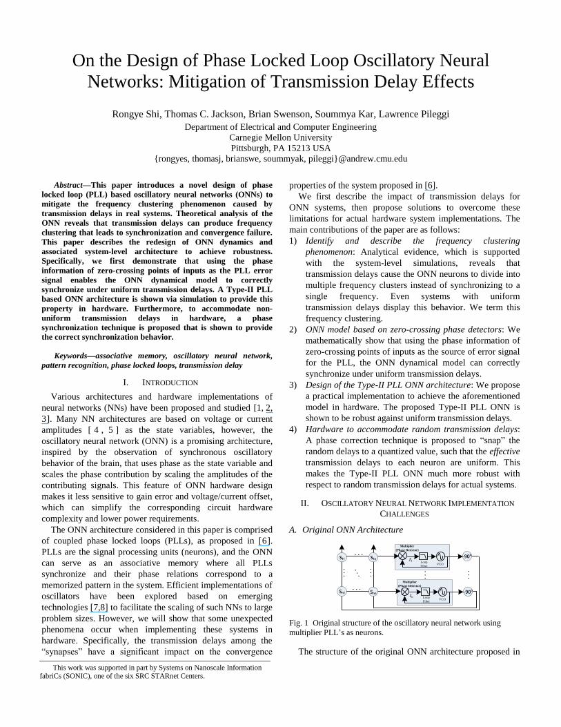
A multiplier-based ONN with 20 neurons was built in
Simulink to test the architecture. The network was trained to
memorize the two patterns shown in Fig. 2. The simulation
shows that with a distorted input, the ONN retrieves the
correct pattern.
Fig. 2 Two patterns are stored in the 20-neuron ONN. If neuron one
serves as the reference, then black pixels represent neurons with 0
degree phase relation w.r.t neuron one, while white pixels represent
neurons with 180 degree phase relation w.r.t neuron one.
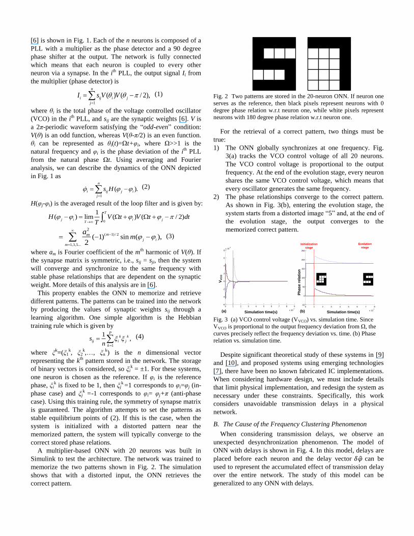
For the retrieval of a correct pattern, two things must be
true:
1) The ONN globally synchronizes at one frequency. Fig.
3(a) tracks the VCO control voltage of all 20 neurons.
The VCO control voltage is proportional to the output
frequency. At the end of the evolution stage, every neuron
shares the same VCO control voltage, which means that
every oscillator generates the same frequency.
2) The phase relationships converge to the correct pattern.
As shown in Fig. 3(b), entering the evolution stage, the
system starts from a distorted image “5” and, at the end of
the evolution stage, the output converges to the
memorized correct pattern.
0 1 2 3 4 5 6 7 8
x 10-7
-50
0
50
100
150
200
250
0 1 2 3 4 5 6 7 8 9
x 10-7
-6
-4
-2
0
2
4
6
8x 10
-3
VV
CO
Ph
as
e r
ela
tio
n
Simulation time(s)
Initialization
stage
Evolution
stage
(b)(a) Simulation time(s) Fig. 3 (a) VCO control voltage (VVCO) vs. simulation time. Since
VVCO is proportional to the output frequency deviation from Ω, the
curves precisely reflect the frequency deviation vs. time. (b) Phase
relation vs. simulation time.
Despite significant theoretical study of these systems in [9]
and [10], and proposed systems using emerging technologies
[7], there have been no known fabricated IC implementations.
When considering hardware design, we must include details
that limit physical implementation, and redesign the system as
necessary under these constraints. Specifically, this work
considers unavoidable transmission delays in a physical
network.
B. The Cause of the Frequency Clustering Phenomenon
When considering transmission delays, we observe an
unexpected desynchronization phenomenon. The model of
ONN with delays is shown in Fig. 4. In this model, delays are
placed before each neuron and the delay vector 𝛿�̂� can be
used to represent the accumulated effect of transmission delay
over the entire network. The study of this model can be
generalized to any ONN with delays.
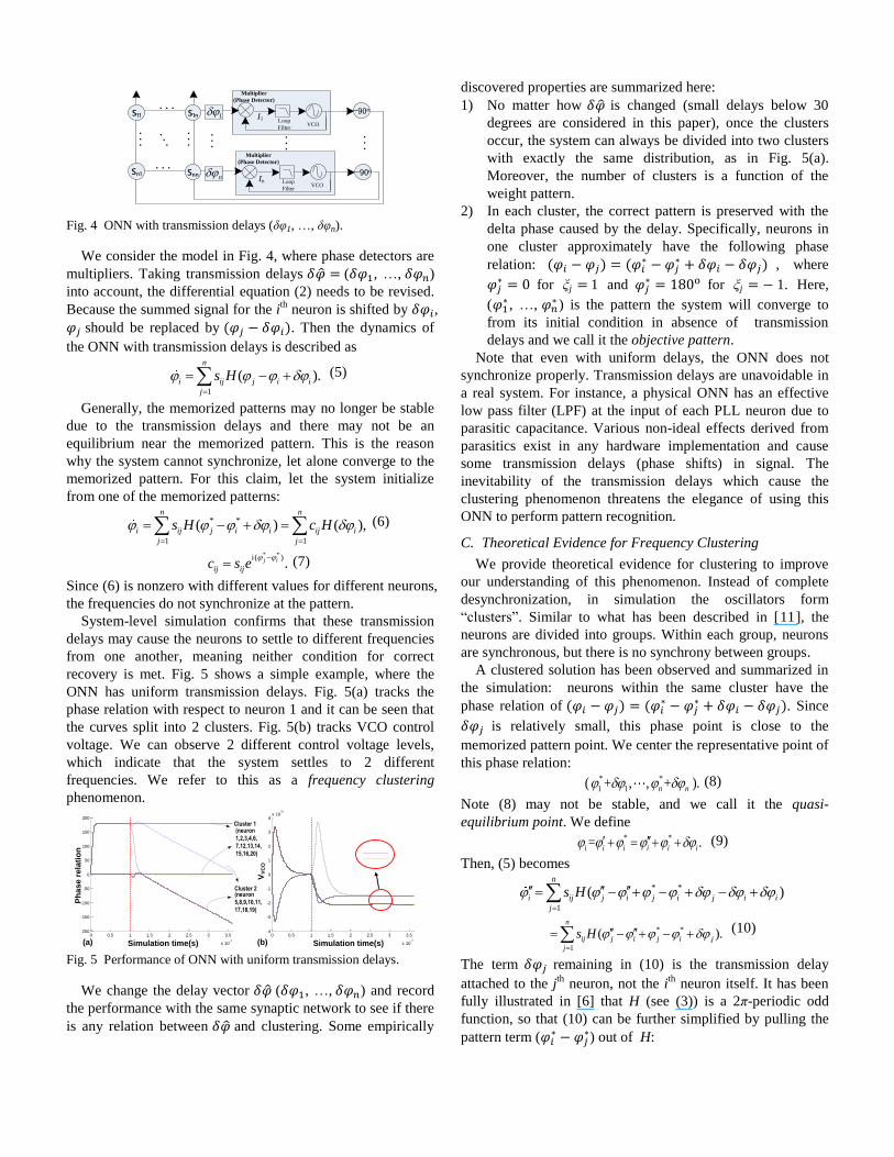
S11 S1n
Sn1 Snn
. . .
-90o
-90o
VCOLoop
Filter
Multiplier
(Phase Detector)
. . .
. . .
. . .
. . .
. . .
. . .Multiplier
(Phase Detector)
Loop
FilterVCO
I1
In
. . .
1
n
Fig. 4 ONN with transmission delays (δφ1, …, δφn).
We consider the model in Fig. 4, where phase detectors are
multipliers. Taking transmission delays 𝛿�̂� = (𝛿𝜑1, …, 𝛿𝜑𝑛)
into account, the differential equation (2) needs to be revised.
Because the summed signal for the ith
neuron is shifted by 𝛿𝜑𝑖,
𝜑𝑗 should be replaced by (𝜑𝑗 − 𝛿𝜑𝑖). Then the dynamics of
the ONN with transmission delays is described as
1
( ).n
i ij j i i
j
s H
(5)
Generally, the memorized patterns may no longer be stable
due to the transmission delays and there may not be an
equilibrium near the memorized pattern. This is the reason
why the system cannot synchronize, let alone converge to the
memorized pattern. For this claim, let the system initialize
from one of the memorized patterns:
* *
1 1
( ) ( ),n n
i ij j i i ij i
j j
s H c H
(6)
* *i( ).j i
ij ijc s e
(7)
Since (6) is nonzero with different values for different neurons,
the frequencies do not synchronize at the pattern.
System-level simulation confirms that these transmission
delays may cause the neurons to settle to different frequencies
from one another, meaning neither condition for correct
recovery is met. Fig. 5 shows a simple example, where the
ONN has uniform transmission delays. Fig. 5(a) tracks the
phase relation with respect to neuron 1 and it can be seen that
the curves split into 2 clusters. Fig. 5(b) tracks VCO control
voltage. We can observe 2 different control voltage levels,
which indicate that the system settles to 2 different
frequencies. We refer to this as a frequency clustering
phenomenon.
0 0.5 1 1.5 2 2.5 3 3.5
x 10-7
-200
-150
-100
-50
0
50
100
150
200
0 0.5 1 1.5 2 2.5 3 3.5
x 10-7
-4
-3
-2
-1
0
1
2
3
4x 10
-3
Simulation time(s) Simulation time(s)
VV
CO
Ph
as
e r
ela
tio
n
(a) (b)
Cluster 1
Cluster 2
(neuron
1,2,3,4,6,
7,12,13,14,
15,16,20)
(neuron
5,8,9,10,11,
17,18,19)
Fig. 5 Performance of ONN with uniform transmission delays.
We change the delay vector 𝛿�̂� (𝛿𝜑1, …, 𝛿𝜑𝑛) and record
the performance with the same synaptic network to see if there
is any relation between 𝛿�̂� and clustering. Some empirically
discovered properties are summarized here:
1) No matter how 𝛿�̂� is changed (small delays below 30
degrees are considered in this paper), once the clusters
occur, the system can always be divided into two clusters
with exactly the same distribution, as in Fig. 5(a).
Moreover, the number of clusters is a function of the
weight pattern.
2) In each cluster, the correct pattern is preserved with the
delta phase caused by the delay. Specifically, neurons in
one cluster approximately have the following phase
relation: (𝜑𝑖 − 𝜑𝑗) = (𝜑𝑖∗ − 𝜑𝑗
∗ + 𝛿𝜑𝑖 − 𝛿𝜑𝑗) , where
𝜑𝑗∗ = 0 for ξj
= 1 and 𝜑𝑗∗ = 180o for ξj
= − 1. Here,
(𝜑1∗ , …, 𝜑𝑛
∗ ) is the pattern the system will converge to
from its initial condition in absence of transmission
delays and we call it the objective pattern.
Note that even with uniform delays, the ONN does not
synchronize properly. Transmission delays are unavoidable in
a real system. For instance, a physical ONN has an effective
low pass filter (LPF) at the input of each PLL neuron due to
parasitic capacitance. Various non-ideal effects derived from
parasitics exist in any hardware implementation and cause
some transmission delays (phase shifts) in signal. The
inevitability of the transmission delays which cause the
clustering phenomenon threatens the elegance of using this
ONN to perform pattern recognition.
C. Theoretical Evidence for Frequency Clustering
We provide theoretical evidence for clustering to improve
our understanding of this phenomenon. Instead of complete
desynchronization, in simulation the oscillators form
“clusters”. Similar to what has been described in [11], the
neurons are divided into groups. Within each group, neurons
are synchronous, but there is no synchrony between groups.
A clustered solution has been observed and summarized in
the simulation: neurons within the same cluster have the
phase relation of (𝜑𝑖 − 𝜑𝑗) = (𝜑𝑖∗ − 𝜑𝑗
∗ + 𝛿𝜑𝑖 − 𝛿𝜑𝑗). Since
𝛿𝜑𝑗 is relatively small, this phase point is close to the
memorized pattern point. We center the representative point of
this phase relation: * *
1 1( + , , + ).n n (8)
Note (8) may not be stable, and we call it the quasi-
equilibrium point. We define * *= .i i i i i i (9)
Then, (5) becomes
* *
1
( )n
i ij j i j i j i i
j
s H
* *
1
( ).n
ij j i j i j
j
s H
(10)
The term 𝛿𝜑𝑗 remaining in (10) is the transmission delay
attached to the jth
neuron, not the ith
neuron itself. It has been
fully illustrated in [6] that H (see (3)) is a 2π-periodic odd
function, so that (10) can be further simplified by pulling the
pattern term (𝜑𝑖∗ − 𝜑𝑗
∗) out of H:
* *i( )
1
( ), .j i
n
i ij j i j ij ij
j
c H c s e
(11)
At the point of (8), (𝜑𝑗′′ − 𝜑𝑖
′′) = 0, and (11) becomes
1
( ).n
i ij j
j
c H
(12)
We denote this value as 𝜔𝑖∗ which represents the frequency
deviation from natural frequency Ω at (8). The matrix made up
of cij is denoted as 𝐂.
We observe that the cluster distribution matches properties
of the matrix 𝐂: as long as the ith
row is the same to the jth
row
in the matrix 𝐂, neuron i and neuron j evolve to the same
cluster in the simulation. For example, if the network is
trained with the patterns “5” and “7” shown in Fig. 2, the
synapse matrix is determined by the Hebbian rule (the term
1/n does not affect the conclusion and is temporarily ignored
here). When image “5” is the objective pattern, according to (7)
and (11), matrix 𝐂 can be determined by scaling the synapse
matrix with pattern “5”. We give the complete matrix 𝐂 for
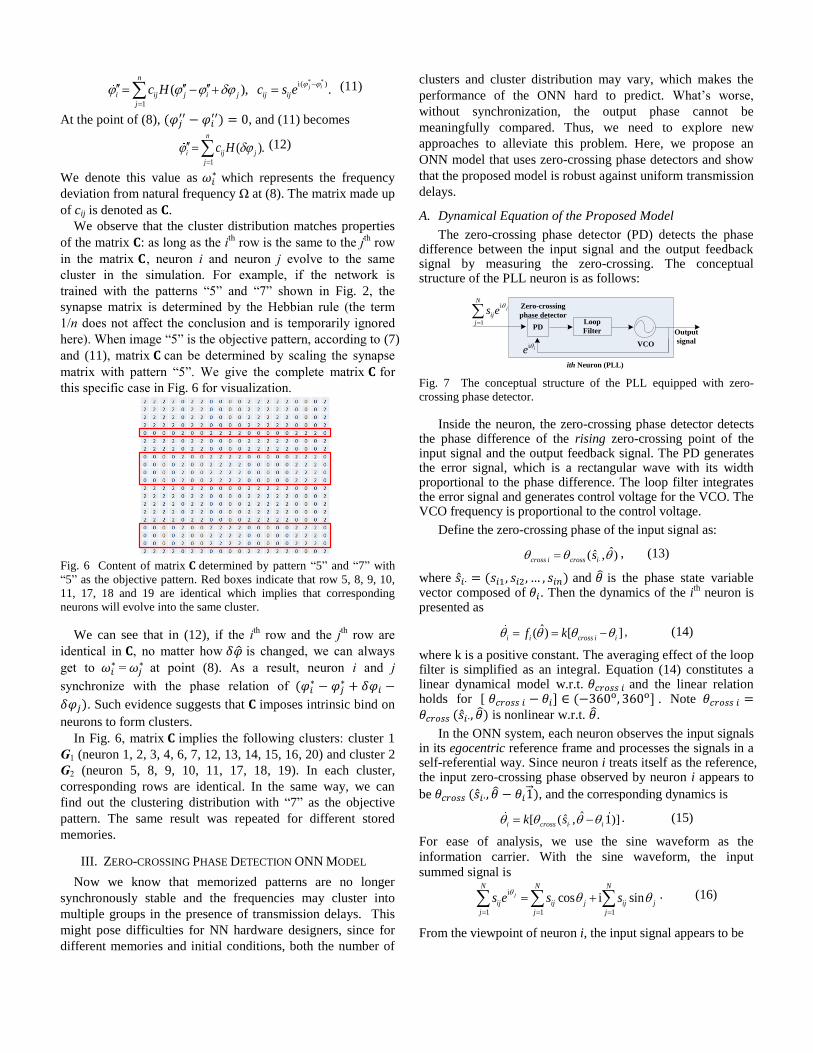
this specific case in Fig. 6 for visualization.
Fig. 6 Content of matrix 𝐂 determined by pattern “5” and “7” with
“5” as the objective pattern. Red boxes indicate that row 5, 8, 9, 10,
11, 17, 18 and 19 are identical which implies that corresponding
neurons will evolve into the same cluster.
We can see that in (12), if the ith
row and the jth
row are
identical in 𝐂, no matter how 𝛿�̂� is changed, we can always
get to 𝜔𝑖∗ = 𝜔𝑗
∗ at point (8). As a result, neuron i and j
synchronize with the phase relation of (𝜑𝑖∗ − 𝜑𝑗
∗ + 𝛿𝜑𝑖 −
𝛿𝜑𝑗). Such evidence suggests that 𝐂 imposes intrinsic bind on
neurons to form clusters.
In Fig. 6, matrix 𝐂 implies the following clusters: cluster 1
G1 (neuron 1, 2, 3, 4, 6, 7, 12, 13, 14, 15, 16, 20) and cluster 2
G2 (neuron 5, 8, 9, 10, 11, 17, 18, 19). In each cluster,
corresponding rows are identical. In the same way, we can
find out the clustering distribution with “7” as the objective
pattern. The same result was repeated for different stored
memories.
III. ZERO-CROSSING PHASE DETECTION ONN MODEL
Now we know that memorized patterns are no longer
synchronously stable and the frequencies may cluster into
multiple groups in the presence of transmission delays. This
might pose difficulties for NN hardware designers, since for
different memories and initial conditions, both the number of
clusters and cluster distribution may vary, which makes the
performance of the ONN hard to predict. What’s worse,
without synchronization, the output phase cannot be
meaningfully compared. Thus, we need to explore new
approaches to alleviate this problem. Here, we propose an
ONN model that uses zero-crossing phase detectors and show
that the proposed model is robust against uniform transmission
delays.
A. Dynamical Equation of the Proposed Model
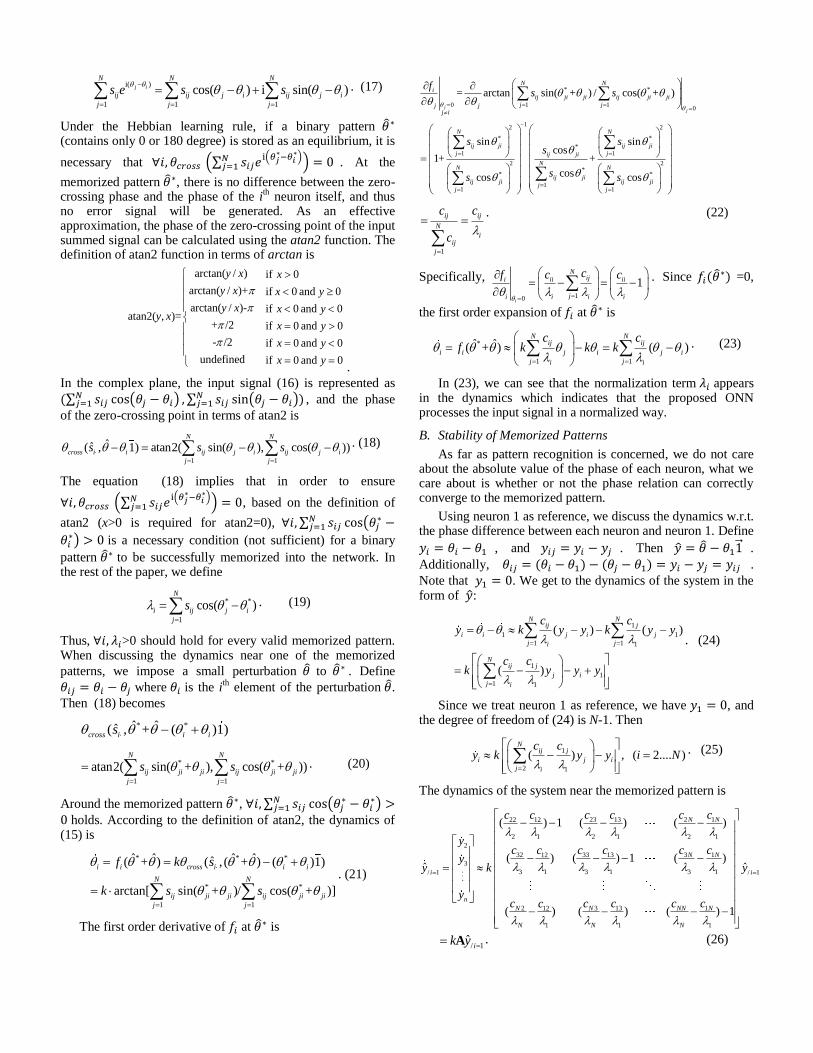
The zero-crossing phase detector (PD) detects the phase difference between the input signal and the output feedback signal by measuring the zero-crossing. The conceptual structure of the PLL neuron is as follows:
Loop
Filter
Zero-crossing
phase detector
VCO
Output
signal
ith Neuron (PLL)
i
1
j
N
ij
j
s e
i ie
PD
Fig. 7 The conceptual structure of the PLL equipped with zero-
crossing phase detector.
Inside the neuron, the zero-crossing phase detector detects the phase difference of the rising zero-crossing point of the input signal and the output feedback signal. The PD generates the error signal, which is a rectangular wave with its width proportional to the phase difference. The loop filter integrates the error signal and generates control voltage for the VCO. The VCO frequency is proportional to the control voltage.
Define the zero-crossing phase of the input signal as:
ˆˆ( , )cross i cross is , (13)
where �̂�𝑖∙ = (𝑠𝑖1, 𝑠𝑖2, … , 𝑠𝑖𝑛) and �̂� is the phase state variable vector composed of 𝜃𝑖. Then the dynamics of the i
th neuron is
presented as
ˆ( ) [ ]i i cross i if k , (14)
where k is a positive constant. The averaging effect of the loop filter is simplified as an integral. Equation (14) constitutes a linear dynamical model w.r.t. 𝜃𝑐𝑟𝑜𝑠𝑠 𝑖 and the linear relation holds for [ 𝜃𝑐𝑟𝑜𝑠𝑠 𝑖 − 𝜃𝑖] ∈ (−360o, 360o] . Note 𝜃𝑐𝑟𝑜𝑠𝑠 𝑖 =𝜃𝑐𝑟𝑜𝑠𝑠 (�̂�𝑖∙, �̂�) is nonlinear w.r.t. �̂�.
In the ONN system, each neuron observes the input signals in its egocentric reference frame and processes the signals in a self-referential way. Since neuron i treats itself as the reference, the input zero-crossing phase observed by neuron i appears to
be 𝜃𝑐𝑟𝑜𝑠𝑠 (�̂�𝑖∙, �̂� − 𝜃𝑖1⃗ ), and the corresponding dynamics is
ˆˆ[ ( , 1)]i cross i ik s . (15)
For ease of analysis, we use the sine waveform as the
information carrier. With the sine waveform, the input
summed signal is
i
1 1 1
cos i sinj
N N N
ij ij j ij j
j j j
s e s s
. (16)
From the viewpoint of neuron i, the input signal appears to be
i( )
1 1 1
cos( ) i sin( )j i
N N N
ij ij j i ij j i
j j j
s e s s
. (17)
Under the Hebbian learning rule, if a binary pattern �̂�∗ (contains only 0 or 180 degree) is stored as an equilibrium, it is
necessary that ∀𝑖, 𝜃𝑐𝑟𝑜𝑠𝑠 (∑ 𝑠𝑖𝑗𝑒i(𝜃𝑗
∗−𝜃𝑖∗)𝑁
𝑗=1 ) = 0 . At the
memorized pattern �̂�∗, there is no difference between the zero-crossing phase and the phase of the i
th neuron itself, and thus
no error signal will be generated. As an effective approximation, the phase of the zero-crossing point of the input summed signal can be calculated using the atan2 function. The definition of atan2 function in terms of arctan is
if 0
if 0 and 0
if 0 and 0
if 0 and 0
if 0 and 0
if 0 and 0
x
x y
x y
x y
x y
x y
arctan( / )
arctan( / )+
arctan( / )-atan2( , )=
+ /2
- /2
undefined
y x
y x
y xy x
.
In the complex plane, the input signal (16) is represented as
(∑ 𝑠𝑖𝑗 cos(𝜃𝑗 − 𝜃𝑖)𝑁𝑗=1 , ∑ 𝑠𝑖𝑗 sin(𝜃𝑗 − 𝜃𝑖)
𝑁𝑗=1 ) , and the phase
of the zero-crossing point in terms of atan2 is
1 1
ˆˆ( , 1) atan2( sin( ), cos( ))N N
cross i i ij j i ij j i
j j
s s s
. (18)
The equation (18) implies that in order to ensure
∀𝑖, 𝜃𝑐𝑟𝑜𝑠𝑠 (∑ 𝑠𝑖𝑗𝑒i(𝜃𝑗
∗−𝜃𝑖∗)𝑁
𝑗=1 ) = 0, based on the definition of
atan2 (x>0 is required for atan2=0), ∀𝑖, ∑ 𝑠𝑖𝑗 cos(𝜃𝑗∗ −𝑁
𝑗=1
𝜃𝑖∗) > 0 is a necessary condition (not sufficient) for a binary
pattern �̂�∗ to be successfully memorized into the network. In the rest of the paper, we define
* *
1
cos( )N
i ij j i
j
s
. (19)
Thus, ∀𝑖, 𝜆𝑖>0 should hold for every valid memorized pattern. When discussing the dynamics near one of the memorized
patterns, we impose a small perturbation �̂� to �̂�∗ . Define
𝜃𝑖𝑗 = 𝜃𝑖 − 𝜃𝑗 where 𝜃𝑖 is the ith element of the perturbation �̂�.
Then (18) becomes
* *ˆ ˆˆ( , + ( )1)cross i i is
* *
1 1
atan2( sin( + ), cos( + ))N N
ij ji ji ij ji ji
j j
s s
. (20)
Around the memorized pattern �̂�∗, ∀𝑖, ∑ 𝑠𝑖𝑗 cos(𝜃𝑗∗ − 𝜃𝑖
∗) >𝑁𝑗=1
0 holds. According to the definition of atan2, the dynamics of (15) is
* * *
* *
1 1
ˆ ˆ ˆ ˆˆ( + ) ( , ( + ) ( )1)
arctan[ sin( + )/ cos( + )]
i i cross i i i
N N
ij ji ji ij ji ji
j j
f k s
k s s
. (21)
The first order derivative of 𝑓𝑖 at �̂�∗ is
* *
1 100
12 2
* *
*1 1
2*
* *
11
= arctan sin( + ) / cos( + )
sin sincos
1+ +
coscos cos
jj
N Ni
ij ji ji ij ji ji
j jj jj i
N N
ij ji ij ji
j jij ji
NN
ij jiij ji ij ji
jj j
fs s
s ss
ss s
2
1
N
1
ij ij
N
iij
j
c c
c
. (22)
Specifically,
10
1
i
Niji ii ii
ji i i i
cf c c
. Since 𝑓𝑖(�̂�∗) =0,
the first order expansion of 𝑓𝑖 at �̂�∗ is
*
1 1
ˆ ˆ( + ) ( )N N
ij ij
i i j i j i
j ji i
c cf k k k
. (23)
In (23), we can see that the normalization term 𝜆𝑖 appears in the dynamics which indicates that the proposed ONN processes the input signal in a normalized way.
B. Stability of Memorized Patterns
As far as pattern recognition is concerned, we do not care about the absolute value of the phase of each neuron, what we care about is whether or not the phase relation can correctly converge to the memorized pattern.
Using neuron 1 as reference, we discuss the dynamics w.r.t. the phase difference between each neuron and neuron 1. Define
𝑦𝑖 = 𝜃𝑖 − 𝜃1 , and 𝑦𝑖𝑗 = 𝑦𝑖 − 𝑦𝑗 . Then �̂� = �̂� − 𝜃11⃗ .
Additionally, 𝜃𝑖𝑗 = (𝜃𝑖 − 𝜃1) − (𝜃𝑗 − 𝜃1) = 𝑦𝑖 − 𝑦𝑗 = 𝑦𝑖𝑗 .
Note that 𝑦1 = 0. We get to the dynamics of the system in the form of �̂�:
1
1 1
1 1 1
1
1
1 1
( ) ( )
( )
N Nij j
i i j i j
j ji
Nij j
j i
j i
c cy k y y k y y
c ck y y y
. (24)
Since we treat neuron 1 as reference, we have 𝑦1 = 0, and the degree of freedom of (24) is N-1. Then
1
2 1
( ) , ( 2.... )N
ij j
i j i
j i
c cy k y y i N
. (25)
The dynamics of the system near the memorized pattern is
23 13 2 122 12
2 1 2 1 2 1
2
32 33 13 3 112
3
3 1 3 1 3 1/ 1 / 1
2 3 13 112
1 1 1
( ) 1 ( ) ( )
( ) ( ) 1 ( )ˆ ˆ
( ) ( ) ( ) 1
N N
N N
i i
n
N N NN N
N N N
c c c cc c
yc c c c cc
yy k y
yc c c c cc
/ 1
ˆik y A . (26)
Once we train the system with Hebbian rule, we obtain the synapse matrix and we can compute A. For the example of patterns “5” and “7” in Fig. 2, numerical analysis shows that the real part of each eigenvalue of A is negative. Based on stability theory [12], patterns “5” and “7” are therefore both stable equilibria of the proposed ONN system.
C. Robustness against Uniform Transmission Delays
When taking uniform transmission delay 𝛿 into account, the
input signal from the view of neuron i is ∑ 𝑠𝑖𝑗𝑒i(𝜃𝑗+𝛿−𝜃𝑖)𝑁
𝑗=1 .
The dynamics near the memorized pattern is
1 1
ˆˆ( , ( 1) 1)
atan2( sin( ), cos( ))
i cross i i
N N
ij ji ij ji
j j
k s
k s s
. (27)
Near the memorized pattern, ∀𝑖, ∑ 𝑠𝑖𝑗 cos(𝜃𝑗𝑖∗ + 𝛿) > 0𝑁
𝑗=1 still
holds. We add a small perturbation �̂� to �̂�∗ , and we have
*
1
*
1
sin( + )
arctan
cos( + )
N
ij ji ji
j
i N
ij ji ji
j
s
k
s
. (28)
It is straightforward to check that 𝑑
𝑑𝛿𝜃𝑐𝑟𝑜𝑠𝑠 = 1, meaning that
near the memorized pattern, 𝜃𝑐𝑟𝑜𝑠𝑠 has a linear relationship to 𝛿. Now, (28) becomes
*
1
*
1
sin( + )
arctan
cos( + )
N
ij ji ji
j
i N
ij ji ji
j
s
k k
s
. (29)
The above equation indicates that at the memorized pattern point, all the neurons have the same frequency offset 𝑘𝛿, the system synchronizes at the frequency of 𝑘𝛿 . Now, let’s consider the dynamics w.r.t �̂�:
1
* *
1 1 1
1 1
* *
1 1 1
1 1
1
2 1
sin( + ) sin( + )
arctan arctan
cos( + ) cos( + )
( )
i i
N N
ij ji ji j j j
j j
N N
ij ji ji j j j
j j
Nij j
j i
j i
y
s s
k k k k
s s
c ck y y
The frequency offset 𝑘𝛿 effectively gets cancelled out and the dynamics is not affected by the uniform transmission delays. The dynamics w.r.t. �̂� remains unchanged
/ 1 / 1ˆ ˆ
i iy k y A .
Therefore, the memorized patterns are also stable equilibria of the system. The proposed ONN is thus robust against uniform transmission delays.
IV. HARDWARE IMPLEMENTATION FOR UNIFORM
TRANSMISSION DELAYS
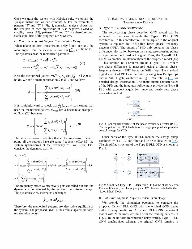
A. Type-II PLL ONN Architecture
The zero-crossing phase detection ONN model can be
achieved in hardware through the Type-II PLL ONN
architecture. In this architecture, the multiplier in the original
system is replaced by D-flip-flop based phase frequency
detector (PFD). The output of PFD only contains the phase
difference information between the rising zero-crossing points
of input signal and feedback signal. Thus, the Type-II PLL
ONN is a practical implementation of the proposed model (15).
This architecture is centered around a Type-II PLL, where
the phase difference is measured using a digital phase-
frequency detector (PFD) based on D-flip-flops. The standard
digital circuit of PFD can be built by using two D-flip-flops
and an “AND” gate, as shown in Fig. 8. We refer to [13] for
detailed design information. The input-output characteristics
of the PFD and the integrator following it provide the Type-II
PLL with excellent acquisition range and nearly zero phase
error when locked.
Clk
D Q
Clk
D Q
V1
V2
VDD
VDD
UP
Down
Clr
Clr
Fig. 8 Conceptual structure of the phase-frequency detector (PFD).
The output of the PFD feeds into a charge pump which provides
control voltage for VCO.
Other parts of the Type-II PLL include the charge pump
combined with a RC loop filter and VCO as detailed in [13].
The simplified structure of the Type-II PLL ONN is shown in
Fig. 9.
VCOLoop
Filter
PFD
S11 S1n
Sn1 Snn
VCOLoop
Filter
Phase Frequency
Detector
. . .
. . .
. . .
. . .
. . .
. . .
PFD
. . .
Phase Frequency
Detector
Fig. 9 Simplified Type-II PLL ONN using PFD as the phase detector.
For simplification, the charge pump and RC filter are included in the
“Loop Filter” block.
B. Robustness against Uniform Transmission Delays
We provide the simulation outcomes to compare the
proposed Type-II PLL ONN with the original ONN under
uniform delay conditions. A Type-II PLL ONN behavioral
model with 20 neurons was built with the training patterns in
Fig. 2. In the uniform transmission delay testing, Type-II PLL
ONN synchronizes whereas the original ONN remains in
clustered states. The uniform transmission delays are set to be
𝛿 =7.2 degree in this example.
In the experiment, the delay values are uniformly set and
the objective pattern is “5”. The objective pattern along with
the synapse matrix determines 𝐂 which suggests how many
clusters are formed and which neuron belongs to which cluster.
Fig. 10 shows the frequency evolution for experiment. The
natural frequency decides the initial frequency. We
compensate this common frequency mode and only consider
the frequency deviation. So when entering evolution stage, all
curves start from zero. The initial condition is pattern “5”.
0 0.5 1 1.5 2 2.5 3 3.5
x 10-7
-10
-8
-6
-4
-2
0
2x 10
-5
0 0.5 1 1.5 2 2.5 3 3.5 4 4.5 5
x 10-7
-4
-3
-2
-1
0
1
2
3
4x 10
-3
VV
CO
(V
)
Simulation time (s)
VV
CO
(V
)
Simulation time (s)
1G
2G
(a) (b)
(neuron 1, 2, 3, 4, 6, 7, 12, 13 14, 15, 16, 20)1G
2G (neuron 5, 8, 9, 10, 11, 17, 18, 19)
Fig. 10 Simulation of VCO control voltage over time for experiment
with “5” as the objective pattern. (a) Behavior of Type-II PLL ONN
architecture. (b) Behavior of original ONN architecture.
In Fig. 10 (a), the normalization feature in the Type-II PLL
removes the frequency difference at the pattern point and the
macro effect is the global synchronization. In Fig. 10 (b), the
original ONN evolves into clustered state. The cluster
distribution precisely matches the property of matrix 𝐂. Due to
the influence of input amplitude, there is no stable equilibrium
near the memorized pattern point.
0 0.1 0.2 0.3 0.4 0.5 0.6 0.7 0.8 0.9 1
x 10-6
-1.5
-1
-0.5
0
0.5
1
1.5
2x 10
-3
0 0.1 0.2 0.3 0.4 0.5 0.6 0.7 0.8 0.9 1
x 10-6
0
20
40
60
80
100
120
140
160
180
200
VV
CO
(V
)
Simulation time (s)Simulation time (s)
Ph
ase
re
latio
n
(b)(a)
Fig. 11 The retrieval of pattern in Type-II PLL ONN with uniform
transmission delays. (a) Phase relation vs. time. (b) VCO control
voltage (VVCO) vs. time.
With uniform transmission delays, the memorized pattern
maintains its stability in Type-II PLL ONN as is proven in
Section III. (C). In Fig. 11, the Type-II PLL ONN system
initializes at a distorted pattern and the correct pattern is
retrieved in the simulation. Due to the delay, there is a
constant frequency offset for all neurons at the end of the
evolution.
V. HARDWARE IMPLEMENTATION FOR RANDOM TRANSMISSION
DELAYS
In an actual hardware system, the transmission delays will be non-uniform. Unfortunately, simulations show that under
random delays, both proposed and original systems fail to synchronize and instead evolve into clusters. What’s worse, the clustering can be affected by different transmission delays, and therefore changes for different weight patterns and hardware variations. Thus, the unknown and complex phase noise environment in real hardware system makes the ONN performance hard to predict.
To tackle this problem, we develop a technique to ensure uniform transmission delays and make the system much more robust against random transmission delays in real system.
A. Phase Correction Technique
The idea of the phase correction technique is to “snap” the
phase shift in the summed signal to a quantized value, such
that the transmission delays viewed by each neuron are
uniform.
This idea can be implemented using a synchronous
comparator clocked at a higher frequency than the neuron
output. The D-flip-flop is a typical circuit for such function.
The D-flip-flop captures the value of the D-input at a defined
portion of the clock cycle (here we choose the rising edge of
the clock). The captured value becomes the Q output. At other
times, the output Q does not change.
PLL1
PLL2
Clk
DQ
Clk
D Q
Clock
Summed
signal 1
Summed
signal 2
Processed
Signal 1
Processed
Signal 2
output1
output2
Fig. 12 Conceptual structure of the phase correction technique with
D-flip-flops.
The conceptual design of the phase correction technique is
shown in Fig. 12. The summed signals are processed by the D-
flip-flop before received by neurons. The clock port (Clk) is
hooked up to a high frequency clock. D-flip-flop samples and
compares the summed signal at every rising edge of the clock.
1
2
con
con
Summed
signal 1
Summed
signal 2
Processed
signal 2
Processed
signal 1
Clock
Fig. 13 Timing diagram showing the mechanism of the phase
correction technique.
The timing diagram in Fig. 13 illustrates the mechanism of
the phase correction technique. Neuron 1 and neuron 2 should
be in-phase under ideal condition, but different transmission
delays (δφ1 and δφ2) distort the phase information in the
summed signals. The D-flip-flop samples the summed signal
at the second rising edge of the clock and delivers this signal
to the neuron. The equivalent effect is that each neuron
receives the summed signal with uniform transmission delay
δφcon. With uniform transmission delays, synchronization will
occur as long as δφi are smaller than the sampling clock period.
This allows a system to be designed with clear metrics for
guaranteeing synchronization that is not dependent on the
synaptic pattern.
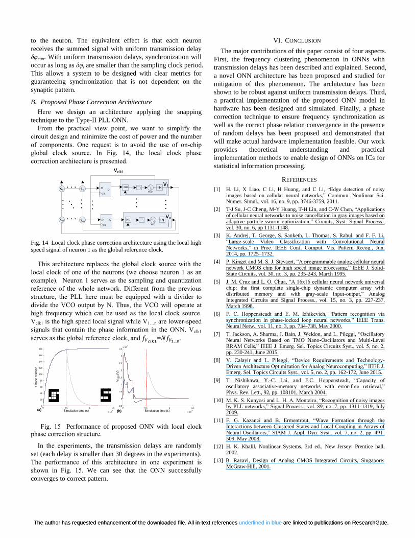
B. Proposed Phase Correction Architecture
Here we design an architecture applying the snapping
technique to the Type-II PLL ONN.
From the practical view point, we want to simplify the
circuit design and minimize the cost of power and the number
of components. One request is to avoid the use of on-chip
global clock source. In Fig. 14, the local clock phase
correction architecture is presented.
VCO
VCOClk
DQS11 S1n
Sn1 Snn
. . .
. . .
. . .
. . .
. . .
. . .
. . .
Clk
D Q
. . .
Vclk1
V1
Vn
PFD
PFD
÷N
÷N
Fig. 14 Local clock phase correction architecture using the local high
speed signal of neuron 1 as the global reference clock.
This architecture replaces the global clock source with the
local clock of one of the neurons (we choose neuron 1 as an
example). Neuron 1 serves as the sampling and quantization
reference of the whole network. Different from the previous
structure, the PLL here must be equipped with a divider to
divide the VCO output by N. Thus, the VCO will operate at
high frequency which can be used as the local clock source.
Vclk1 is the high speed local signal while V1…n are lower-speed
signals that contain the phase information in the ONN. Vclk1
serves as the global reference clock, and 𝑓𝑉𝑐𝑙𝑘1=𝑁𝑓𝑉1…𝑛
.
0 0.5 1 1.5
x 10-6
-0.5
0
0.5
1
1.5
2
2.5
3
3.5x 10
-3
0 0.5 1 1.5
x 10-6
0
20
40
60
80
100
120
140
160
180
VV
CO
(V
)
Simulation time (s)Simulation time (s)
Ph
ase
re
latio
n
(b)(a)
Fig. 15 Performance of proposed ONN with local clock phase correction structure.
In the experiments, the transmission delays are randomly
set (each delay is smaller than 30 degrees in the experiments).
The performance of this architecture in one experiment is
shown in Fig. 15. We can see that the ONN successfully
converges to correct pattern.
VI. CONCLUSION
The major contributions of this paper consist of four aspects.
First, the frequency clustering phenomenon in ONNs with
transmission delays has been described and explained. Second,
a novel ONN architecture has been proposed and studied for
mitigation of this phenomenon. The architecture has been
shown to be robust against uniform transmission delays. Third,
a practical implementation of the proposed ONN model in
hardware has been designed and simulated. Finally, a phase
correction technique to ensure frequency synchronization as
well as the correct phase relation convergence in the presence
of random delays has been proposed and demonstrated that
will make actual hardware implementation feasible. Our work
provides theoretical understanding and practical
implementation methods to enable design of ONNs on ICs for
statistical information processing.
REFERENCES
[1] H. Li, X Liao, C Li, H Huang, and C Li, “Edge detection of noisy images based on cellular neural networks,” Commun. Nonlinear Sci. Numer. Simul., vol. 16, no. 9, pp. 3746-3759, 2011.
[2] T-J Su, J-C Cheng, M-Y Huang, T-H Lin, and C-W Chen, “Applications of cellular neural networks to noise cancellation in gray images based on adaptive particle-swarm optimization,” Circuits, Syst. Signal Process., vol. 30, no. 6, pp 1131-1148.
[3] K. Andrej, T. George, S. Sanketh, L. Thomas, S. Rahul, and F. F. Li, “Large-scale Video Classification with Convolutional Neural Networks,” in Proc. IEEE Conf. Comput. Vis. Pattern Recog., Jun. 2014, pp. 1725–1732.
[4] P. Kinget and M. S. J. Steyaert, “A programmable analog cellular neural network CMOS chip for high speed image processing,” IEEE J. Solid-State Circuits, vol. 30, no. 3, pp. 235-243, March 1995.
[5] J. M. Cruz and L. O. Chua, “A 16x16 cellular neural network universal chip: the first complete single-chip dynamic computer array with distributed memory and with gray-scale input-output,” Analog Integrated Circuits and Signal Process., vol. 15, no. 3, pp. 227-237, March 1998.
[6] F. C. Hoppensteadt and E. M. Izhikevich, “Pattern recognition via synchronization in phase-locked loop neural networks,” IEEE Trans. Neural Netw., vol. 11, no. 3, pp. 734-738, May 2000.
[7] T. Jackson, A. Sharma, J. Bain, J. Weldon, and L. Pileggi, “Oscillatory Neural Networks Based on TMO Nano-Oscillators and Multi-Level RRAM Cells,” IEEE J. Emerg. Sel. Topics Circuits Syst., vol. 5, no. 2, pp. 230-241, June 2015.
[8] V. Calayir and L. Pileggi, “Device Requirements and Technology- Driven Architecture Optimization for Analog Neurocomputing,” IEEE J. Emerg. Sel. Topics Circuits Syst., vol. 5, no. 2, pp. 162-172, June 2015.
[9] T. Nishikawa, Y.-C. Lai, and F.C. Hoppensteadt, “Capacity of oscillatory associative-memory networks with error-free retrieval,” Phys. Rev. Lett., 92, pp. 108101, March 2004.
[10] M. K. S. Kunyosi and L. H. A. Monteiro, “Recognition of noisy images by PLL networks,” Signal Process., vol. 89, no. 7, pp. 1311-1319, July 2009.
[11] F. G. Kazanci and B. Ermentrout, “Wave Formation through the Interactions between Clustered States and Local Coupling in Arrays of Neural Oscillators,” SIAM J. Appl. Dyn. Syst., vol. 7, no. 2, pp. 491-509, May 2008.
[12] H. K. Khalil, Nonlinear Systems, 3rd ed., New Jersey: Prentice hall, 2002.
[13] B. Razavi, Design of Analog CMOS Integrated Circuits, Singapore: McGraw-Hill, 2001.
The author has requested enhancement of the downloaded file. All in-text references underlined in blue are linked to publications on ResearchGate.The author has requested enhancement of the downloaded file. All in-text references underlined in blue are linked to publications on ResearchGate.


![DESIGN AND ANALYSIS OF EFFICIENT PHASE LOCKED LOOP … · Phase Locked Loop (PLL) mainly for synchronization, clock synthesis, skew and jitter reduction [5]. Phase locked loops find](https://img.pdfslide.us/doc/110x75/5e9d540ca2a49a4e746bfacd/design-and-analysis-of-efficient-phase-locked-loop-phase-locked-loop-pll-mainly.jpg)