Embed Size (px)
Citation preview

On-focal-plane ADC: Recent progress at JPL
Zhimin Zhou, Bedabrata Pain, Roger Panicacci, Bamiak Mansoorian, Junichi Nakamura, and Eric R. Fossum
Center for Space Microelectronics TechnologyJet Propulsion Laboratory - California Institute of Technology
4800 Oak Grove Drive, Pasadena, CA 91109
O1ympus America Inc., Torrance, CA 90505
ABSTRACT
Two 8 bit successive approximation analog-to-digital converters (ADC), an 8 bit single slope ADC, and a 12 bit currentmode incremental sigma delta (E-A) ADC have been designed, fabricated, and tested. The 20.4 jtm and 40 jtm pitchsuccessive approximation test chip designs are compatible with active pixel sensor (APS) column parallel architectures. A 64x 64 photogate APS with this ADC integrated on-chip was fabricated in a 1.2 .tm N-well CMOS process and achieves 8 bitaccuracy. A 1K x 1K APS with 1 1 im pixels and a single slope ADC in each column was fabrciated in a 0.55 tmN-wellCMOS process and also achieves 8 bit accuracy. The successive approximation designs consumeas little as 49 j.tW at a 500KHz conversion rate meeting the low power requirements inherent in column parallel architectures. The current modeADC test chip is designed to be multiplexed among 8 columns in a semi-column parallel current mode APS architecture. Itconsumes 800 jiW at a 5 KHz conversion rate.
1. INTRODUCTION
A key advantage to CMOS image sensors is the ability to integrate readout electronics on the same focal plane as the sensoras shown in figure 1 . Through the use of standard CMOS technology there is available a wide variety of approaches toanalog to digital conversion12'3'4'5'6'7. Sensor chip architectures placing analog to digital converters (ADC) in each columnoffer parallel conversion of an entire row of pixel data. This parallelism reduces the requirement for high speed ADCs(figure 1). For example, the minimum conversion speed ofan ADC in each column ofa 1024 x 1024 image sensor operatingat a 30 Hz frame rate is approximately 33 KHz. Overhead for transferring off-chip the resultant digital image data canincrease this speed requirement but can be overcome using either pipelined data transfer during the conversion or a highbandwidth digital output port.
1000.0
rowselect APS ARRAYlogic
-ADC ARRAY
I I I IIcolumn readout
select logic
ND conversion rate (KHz)
Figure 1. Frame rate vs. AJJC speedfor a 512x512, 1024x1024, and 2048x2048 APS with the above column parallelarchitectureforfocaiplane AIDconversion (1.5 sec row access time assumed).
A design tradeoff in placing an ADC per column is the low power requirement and increased physical size resulting from thesmall column pitch (10 to 40 jim depending on the process technology). A small pitch can also lead to column to columnvariations in ADC response because of poor device matching. To minimize these problems a compromise is possible, for
O-8194-2126-X/96/$6.OO SP!E Vol. 2745 1 111
515100.0
. 10.0C) _________________________________E ______________________________
—1024x1024.-.
1.01 ______________________________
—&—2048x2048
0.1 I
I 10 100 1000
example, by multiplexing a single ADC per 8 columns.
Because both voltage mode and current mode active pixel sensors are used, there is a need for both voltage and current modeADCs. The two successive approximation ADCs presented below operate in voltage mode and the sigma-delta ADCoperates in a current mode. The successive approximation designs physically fit into a per column architecture and thesigma-delta fits onto an 8 column pitch where its operation is multiplexed.
The design and test resultsfor each ADC are presented below. Section 2 reviews one of the first approaches used in columnparallel ADC architectures'7 and presents a 1K x 1K image sensor using this ADC. Section 3 describes the operation and testresults of a successive approximation ADC approach using switched capacitor op amp integrators. Section 4 presents asuccessive approximation ADC based on charge redistribution on a network of binary scaled capacitors. Also presented is a64 x 64 CMOS APS with this ADC implemented on chip. Section 5 describes the operation and test results of the currentmode sigma-delta ADC. Section 6 contains a summary ofthe four design characteristics.
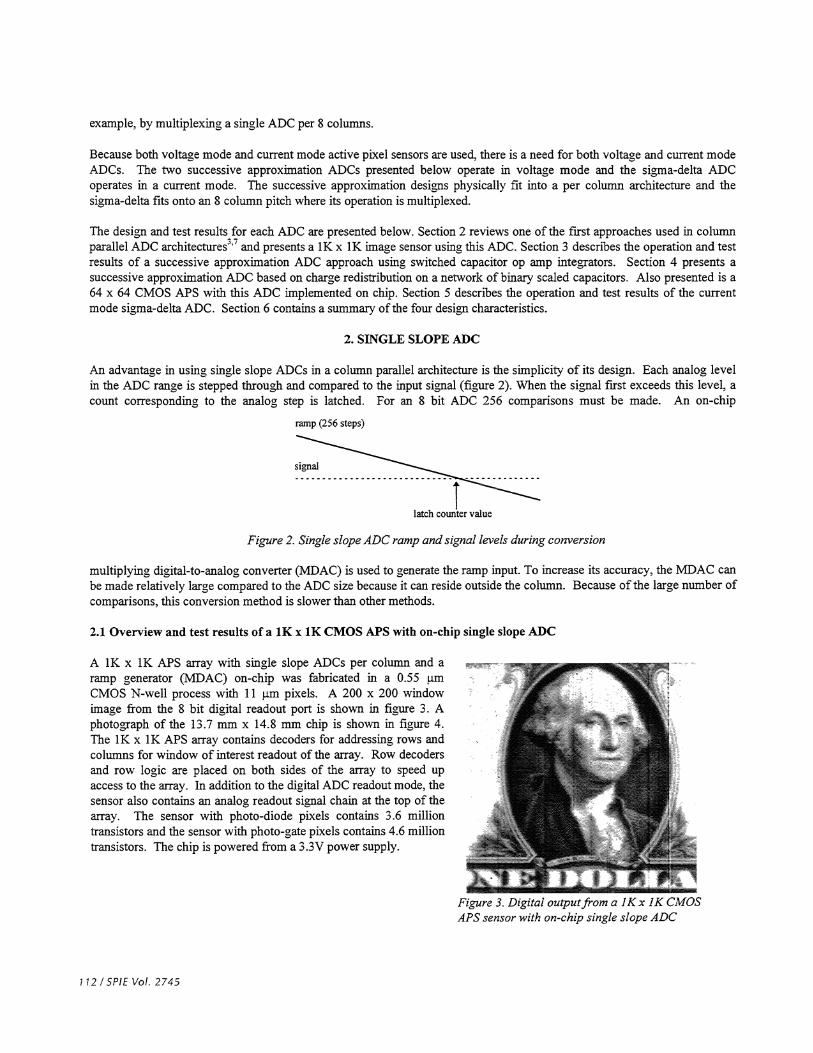
2. SINGLE SLOPE ADC
An advantage in using single slope ADCs in a column parallel architecture is the simplicity of its design. Each analog levelin the ADC range is stepped through and compared to the input signal (figure 2). When the signal first exceeds this level, acount corresponding to the analog step is latched. For an 8 bit ADC 256 comparisons must be made. An on-chip
ramp (256 steps)
latch counter value
Figure 2. Single slope ADC ramp andsignal levels during conversion
multiplying digital-to-analog converter (MDAC) is used to generate the ramp input. To increase its accuracy, the MDAC canbe made relatively large compared to the ADC size because it can reside outside the column. Because of the large number ofcomparisons, this conversion method is slower than other methods.
2.1 Overview and test results of a 1K x 1K CMOS APS with on-chip single slope ADC
A 1K x 1K APS array with single slope ADCs per column and aramp generator (MDAC) on-chip was fabricated in a 0.55 .tmCMOS N-well process with 1 1 .tm pixels. A 200 x 200 windowimage from the 8 bit digital readout port is shown in figure 3 . Aphotograph of the 13.7 mm x 14.8 mm chip is shown in figure 4.The 1K x 1K APS array contains decoders for addressing rows andcolumns for window of interest readout of the array. Row decodersand row logic are placed on both sides of the array to speed upaccess to the array. In addition to the digital ADC readout mode, thesensor also contains an analog readout signal chain at the top of thearray. The sensor with photo-diode pixels contains 3.6 milliontransistors and the sensor with photo-gate pixels contains 4.6 milliontransistors. The chip is powered from a 3.3V power supply.
112 ISPIE Vol. 2745
Figure 3. Digital outputfrom a 1K x 1K CMOSAPS sensor with on-chip single slope ADC
The per column 8 bit ADCs were characterized through a test port to the input of each ADC. Off chip counters are used asinputs to the ADC latches and MDAC circuit. For ADC characterization the 8 bit digital output of the ADC was passedthrough an off chip 8 bit DAC for convenient display on an oscilloscope and capture by the host computer test system. Thetest system also generates the signal input to the ADC through the test port.
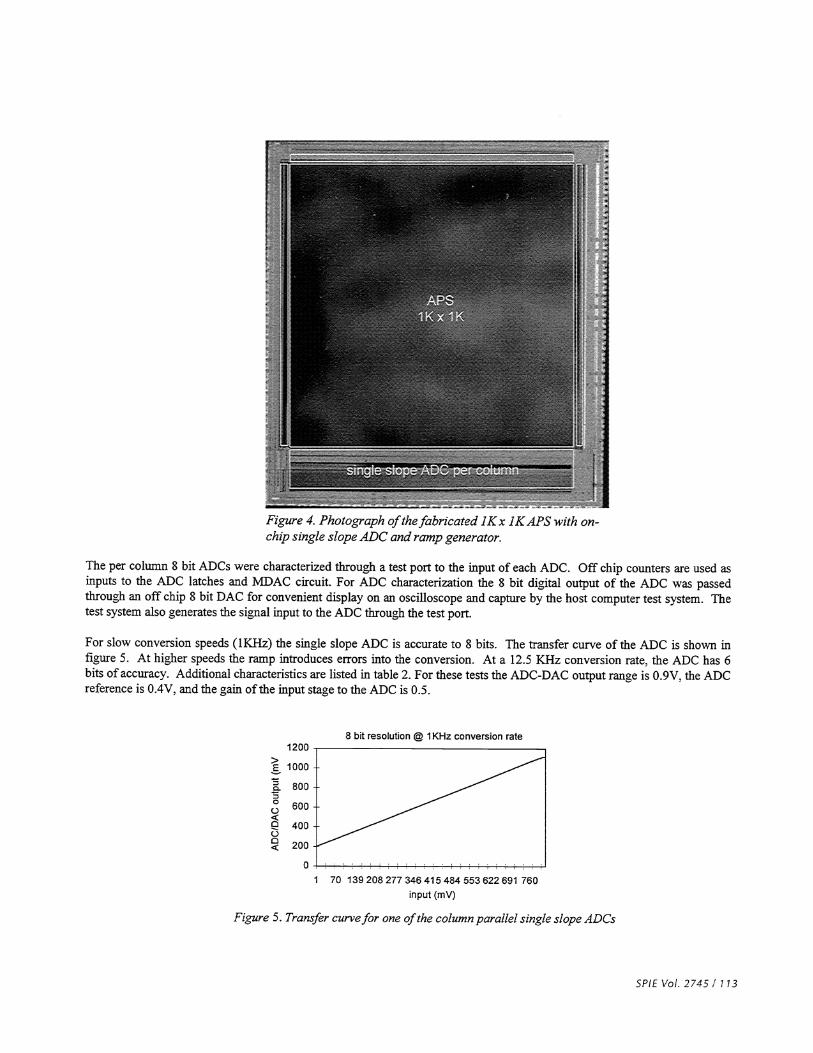
For slow conversion speeds (1KHz) the single slope ADC is accurate to 8 bits. The transfer curve of the ADC is shown infigure 5. At higher speeds the ramp introduces errors into the conversion. At a 12.5 KHz conversion rate, the ADC has 6bits of accuracy. Additional characteristics are listed in table 2. For these tests the ADC-DAC output range is 0.9V, the ADCreference is 0.4V, and the gain of the input stage to the ADC is 0.5.
1200
1000
0600
Q 40000< 2000
1 70 139208277346415484 553622691 760input (mV)
SPIE Vol. 2745 / 113
Figure 4. Photograph of the fabricated lKx JKAPS with on-chip single slope ADC and ramp generator.
8 bit resolution @ I KHz conversion rate
Figure 5. Transfer curve for one of the column parallel single slope ADCs

3. SWITCHED-CAPACITOR SUCCESSIVE APPROXIMATION ADC
The successive approximation approach to analog-to-digital conversion is essentially a "ranging" algorithm. The new featurein the successive approximation ADCs presented below is the double sided approach to conversion. The ADC attempts toadd successive binary fractions of a reference voltage to either the pixel signal or reset level until they are equal. In this wayif a comparison result is false, the ADC saves a step by not having to remove the previously added reference fraction fromthe signal. The ADC was designed for an APS sensor with a readout scheme where the pixel reset voltage is greater than thepixel signal level as in [8]. The voltage levels at each step "i" in the conversion are shown in figure 6 and are described by:
V,1=V5,1_1+bLJ
VR,=VR,_l+bI
reset—I
b = 0 if VRl < V,1.1= 1 if VR,l > Vs,il signal
Figure 6. InternalADC sampled reset andsignal levels during conversion
3.1 Design and operation
The first design approach uses two switched-capacitor integrators to perform the successive approximation analog to digitalconversion. This successive approximation method attempts to fmd the digital representation of the pixel signal relative tothe pixel reset level. It does this conversion by successively adding binary scaled fractions of a reference voltage to eitherthe readout pixel signal voltage or pixel reset voltage until the two values are equal to within the desired accuracy or oneleast significant bit (LSB).
The schematic of the ADC is shown in figure 7. The ADC has two inputs for pixel signal and reset levels (VS and VR).There is also an input for the ADC voltage reference range. All input voltages are referenced to V+. The top op ampintegrator stores the pixel signal level and the bottom op amp integrator stores the reset level. Both integrators are inputs to acomparator. During the ON interval the pixel signal level, reset level, and ADC reference are sampled onto the 2.5 pFcapacitors Cl and C2. The top and bottom integrators are reset to V+ during cI and 1R' respectively. The signal level, VS-V+, is sent to the top integrator input during the Is/ts interval. With a 5 pF op amp feedback capacitor, the integrator gainis -1. Thus, the value V+ -VS is added to integrator output voltage. The reset level, V+-VR, is similarly added to the bottomintegrator output during the RIR interval. The reference level (Vref-V+) is stored on Cl and C2 during I�F.
After the inputs are read into the ADC, CION turns off and the first comparison is performed to determine the sign bit(typically 0 for the image sensor). The comparator is activated when the STRB* signal goes low. Otherwise both comparatoroutputs are 0. If the signal side is greater than the reset side, the comparator output into the shift register is a 0. In thiscase,the feedback from the comparator output sets the switches on the front end to steer the reference on C2 to the integrator onthe reset side holding the lower output voltage. Because Cl is cutoff from C2 during this time, the gain of the integrator is-0.5 (= 2.5pFI5pF). Thus, (V+-Vref)12 is added to the integrator output. For correct operation V+> Vref so that the voltageis increased on integrator with the lower output voltage.
114/SPIE Vol. 2745

During the second comparison, the MSB is determined and stored in the shift register. Before this comparison is performed,the feedback path from the comparator is shut off disconnecting the inputs to the integrator. During the comparison half thecharge on Cl is transferred to C2. The resulting voltage across on C2 is (Vref-V+)/2. Subsequently, Cl is cutoff from C2,the comparison is made, and (V+-Vref)/4 is transferred to the output of the integrator with the lower output voltage (resetside if the original pixel signal is more than 1 MSB larger than the reset level, otherwise to the signal side).
The binary scaled fraction of the reference voltage is always added to the integrator with the lower voltage stored on it. Theintegration and comparison steps are performed until the desired number of bits is achieved. A shift register per columnstores the comparator output for readout of the digital word at the end of the conversion.
One of the key components in this design is the switched capacitor integrator. To achieve at least 8 bit resolution, an op ampwith a gain of 60 dB (1,000) is required'. The op amp used in this design is a single stage folded cascode op amp.
3.2 Test results
The ADC was characterized using a 1V ramp to drive the input from a computer controlled data generator/acquisition board.
1000
> -100-200
0. -
• -400o -500
-600E3 -700o -800
-900-1000
input(V)
SPIE Vol. 2745 / 115
Figure 7. Successive approximation ADCcircuitusing switched capacitor integrators
(0 (N (0 (0 (N (0 (0 (N (0(0 0) C) (0 C) N- (N 0 0) (N (0C Q Q ° N- (0 (0 U) U)
(N (N (N (N (N (N (N (N
8 bit resolution @ 1 0 KHz conversion rate
Figure 8. Transfer curve for a successive approximation ADC implemented with switchedcapacitor circuits.

The analog input was incremented in lmV steps and 500 ADC output samples at each step were acquired. ADC output waspassed through a digital-to-analog converter (DAC). The analog output of the ADCIDAC was connected to the computeracquisition board where it was measured. The DAC has an offset voltage of OV and a —1V reference.
The ADC was characterized at different speeds and power levels. Because of the application of this ADC to the columnparallel architecture ofa CMOS image sensor, the maximum power dissipation desirable from the ADC is approximately 150to 200 j.tW. At these power levels, the ADCs in a 1K x 1K image sensor consume 150 to 200 mW.
For a power dissipation of 1 75 .tW and 8 bit resolution, the maximum conversion rate is 50 KHz or 20 jiseconds/conversion.The maximum 1K x 1K sensor frame rate for this conversion speed is approximately 45 Hz. Integral non-linearity (1NL),differential non-linearity (DNL), and ADC noise were measured (Table 2). The ADC noise is determined from the worstcase standard deviation calculated from the 500 samples taken at each input step. Based on the non-linearites, the effectiveADC accuracy is 5 bits. The ADC operating at a 10 KHz conversion rate worked at a minimum power of 27 iW. Itseffective accuracy is also 5 bits. The transfer curve for the ADC operating under best case conditions at 10 KHz and 134 iWpower level is shown in figure 8.
Stand alone op amps on the test chip were characterized at various power levels. The op amp had a gain of 74 dB andconsumed 70 jW. At a low power dissipation level of 20 iW, the op amp had a gain of 80 dB. However, at the lowbiascurrent levels, the op amp slew rate limited the ADC speed.
4. BINARY SCALED CAPACITOR SUCCESSIVE APPROXIMATION ADC
This approach to ADC design uses a dual networks of binary scaled capacitors to sample pixel signal and reset voltages.These capacitor networks are connected to the input of a comparator. After clamping these levels on the top plate of thecapacitors, the bottom plates are successively connected to the ADC reference voltage. The voltage increase on the top plateis proportional to the relative size ofthe capacitor to the total capacitance ofthe network. The comparator output determineswhich side sees an increase in the top voltage similarly to the switched capacitor integrator approach. This method of usingbinary scaled capacitors to perform analog to digital conversion is similar to [9]. This ADC uses the same new feature as theswitched capacitor design presented in the previous section where a double sided approach is used to increase converterspeed.
4.1 Design and operation
S
R
The block diagram of the dual sided binary scaled capacitor successive approximation ADC is shown in figure 9. Each ofthe latches (BS#9-BR#0) contains a switch either to ground or to the ADC voltage reference as shown in figure 10. If theenable to the latch BS#n on the signal side is active and the comparator output is high (reset input > signal input at thecomparator), the bottom plate of the capacitor is switched from 0 to Vreference. If the same enable to the latch BR#n on thereset side is active and the comparator output is low (signal input> reset input at the comparator), the bottom plate of the
116 ISPIE Vol. 2745
PHIS BS1 BOl BS1O BOlO BCSI BCO1 BCS5 BCO5
Figure 9. Binary scaled capacitor successive approximation ADC
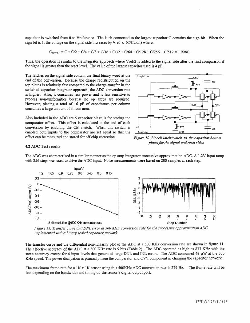
capacitor is switched from 0 to Vreference. The latch connected to the largest capacitor C contains the sign bit. When thesign bit is 1 , the voltage on the signal side increases by Vref x (C/Ctotal) where:
CTOTAL=C+C/2 +C14+C18 +C/16+C/32+C/64+C/128 +C/256+C/512= l.998C.
Thus, the operation is similar to the integrator approach where VrefY2 is added to the signal side after the first comparison ifthe signal is greater than the reset level. The value of the largest capacitor used is 4 pF.
The latches on the signal side contain the fmal binary word at the S
end of the conversion. Because the charge redistribution on thetop plates is relatively fast compared to the charge transfer in theswitched capacitor integrator approach, the ADC conversion rateis higher. Also, it consumes less power and is less sensitive toprocess non-uniformities because no op amps are required.However, placing a total of 16 pF of capacitance per columnconsumes a large amount of silicon area.
Also included in the ADC are 5 capacitor bit cells for storing thecomparator offset. This offset is calculated at the end of eachconversion by enabling the CB switch. When this switch isenabled both inputs to the comparator are set equal so that the _____________________________________________offset can be measured and stored for off chip correction.
4.2 ADC Test results
The ADC was characterized in a similar manner as the op amp integrator successive approximation ADC. A l.2V input rampwith 256 steps was used to drive the ADC input. Noise measurements were based on 200 samples at each step.
1.2 1.05 0.9 0.75 0.6 0.45 0.3 0.15
0.2 2
,—.. 0 1
-0.2.-0.4C
-0.6 O33-0.8 -4
< -1 -5
-1.28 bft resokion @500 KHZ converon rate Step Number
Figure 1 1. Transfer cur'e and DNL error at 500 KT-Iz conversion ratefor the successive approximation ADCimplemented with a binary scaled capacitor network
The transfer curve and the differential non-linearity plot of the ADC at a 500 KHz conversion rate are shown in figure 11.The effective accuracy of the ADC at a 500 KHz rate is 5 bits (Table 2). The ADC operated as high as 833 KHz with thesame accuracy except for 4 input levels that generated large DNL and 1NL errors. The ADC consumed 49 W at the 500KHz speed. The power dissipation is primarily from the comparator and CV2f component in charging the capacitor network.
The maximum frame rate for a 1K x 1K sensor using this 500KHz ADC conversion rate is 279 Hz. The frame rate will beless depending on the bandwidth and timing of the sensor's digital output port.
SPIE Vol. 2745 / 117
Figure 10. Bit cell latcWswitch to the capacitor bottomplates for the signal and reset sides
o C%J (0 (0 0 C\J (0C') (0 0) Ci (0 0) ('.1 (0
c\J C4

4.3 Test results from a CMOS APS imager with on-chip ADC
A variation in the ADC design using only a single bank of capacitors on the signal side was integrated with a 64 x 64 CMOSactive pixel image sensor. The operation ofthe adc is similar to the double sided capacitor approach but operates only on thesignal level during conversion (figure 12).
reset
signal
Figure 12. Timing of internalADC sampled reset and signal levels
during conversionfor a single bank ofcapacitors on the signal side.
This design was fabricated in a 1.2 pm N-well CMOS process with linear capacitors. The 8 bit ADC size is 24 j.tm x 2.2mm. The photogate pixel is 24 m x 24 .tm. An 8 bit image from a 64 x 32 window from the sensor is shown in figure 13.A decoder is used to address rows and columns in the array to generate the window of interest readout. A photograph of the3.0 mm x 5.0 mm chip is shown in figure 14.
The ADC integrated on-chip was operated without using the offset correction bits. In this mode the ADC has less than 2LSBs of fixed pattern noise across the 64 column parallel ADC array. This corresponds to a maximum of 7 mV of variationin the comparator input offset voltage from column to column.
The ADCs were characterized through a test port connecteddirectly into the ADC input. At a 70 KHz conversion rate,the measured INL was 1 LSB and the DNL was 0.8 LSB.
Although the single sided capacitor network approach isslower than the double sided approach, it requires much lessarea. The accuracy is also better because the capacitormatching requirement between the two banks is eliminated.
Figure 13. 64 x 32 APS image with on-ch4, successive approximation ADC.
118/SPIEVo/. 2745
Figure 14. Photograph offabricated 64 x 64 active pixelsensor with on-chip successive approximation ADC.
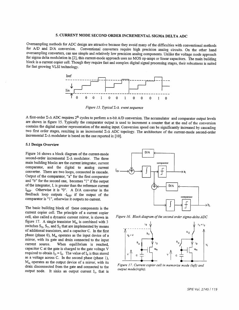
5. CURRENT MODE SECOND ORDER INCREMENTAL SIGMA DELTA ADC
Oversampling methods for ADC design are attractive because they avoid many ofthe difficulties with conventional methodsfor AID and DIA conversion. Conventional converters require high precision analog circuits. On the other handoversampling converters, can use simple and relatively low precision analog components. Unlike the voltage mode approachfor sigma delta modulation in [2], this current-mode approach uses no MOS op-amps or linear capacitors. The mainbuildingblock is a current copier cell. Though they require fast and complex digital signal processing stages, their robustness is suitedfor fast growing VLSI technology.
Figure 15. Typical E-z event sequence
A first-order ADCrequires 2 cycles to perform a n-bit A/D conversion. The accumulator and comparator output levelsare shown in figure 15. Typically the comparator output is used to increment a counter that at the end of the conversioncontains the digital number representation of the analog input. Conversion speed can be significantly increased by cascadingtwo first order stages, resulting in an incremental ADC topology. The architecture of the current-mode second-orderincremental Z- modulator is based on the one reported in [10].
5.1 Design Overview
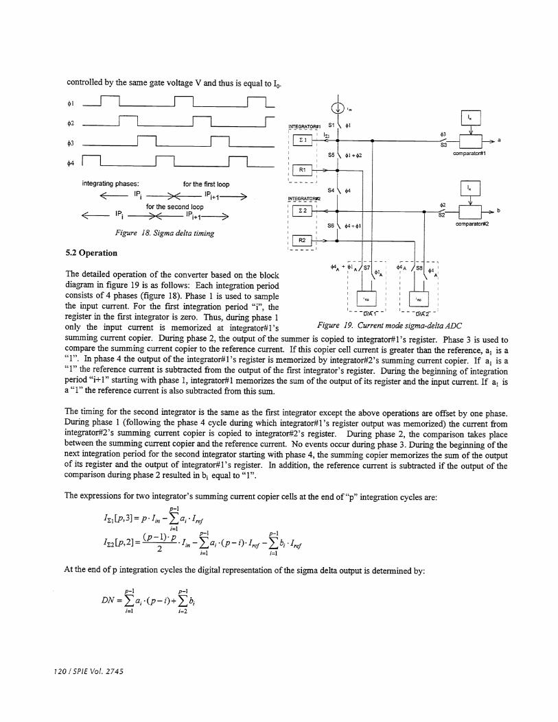
Figure 1 6 shows a block diagram of the current-modesecond-order incremental E-i modulator. The threemain building blocks are the current integrator, currentcomparator, and the digital to analog currentconverter. There are two loops, connected in cascade.Output of the comparator, "a" for the first comparatorand "b" for the second one, becomes "1 " if the outputofthe integrator, I, is greater than the reference current'REF Otherwise it is "0". A DIA converter in thefeedback loop outputs 'REF if the output of thecomparator is "1", otherwise it outputs no current.
bThe basic building block of these components is thecurrent copier cell. The principle of a current copiercell, also called a dynamic current mirror, is shown infigure 17. A single transistor Mm is combined with 3switches S, and Sz that are implemented by meansof additional transistors, and a capacitor C. In the firstphase (phase 0), Mm operates as the input device of amirror, with its gate and drain connected to the inputcurrent source. When equilibrium is reached,capacitor C at the gate is charged to the gate voltage Vrequired to obtain 'D = Jo. The value of I is thus storedas a voltage across C. In the second phase (phase 1),Mm operates as the output device of a mirror, with itsdrain disconnected from the gate and connected to theoutput node. It sinks an output current I, that is
SPIE Vol. 2745 / 119
a
Figure 16. Block diagram of the second order sigma-delta ADC
Figure 17. Current copier cell in memorize mode (left) andoutput mode (right).
controlled by the same gate voltage V and thus is equal to J.
for the first loop
S7 A
'—ci-'Figure 19. Current mode sigma-delta ADC
b
The detailed operation of the converter based on the blockdiagram in figure 19 is as follows: Each integration periodconsists of 4 phases (figure 18). Phase 1 is used to samplethe input current. For the first integration period "i", theregister in the first integrator is zero. Thus, during phase 1only the input current is memorized at integrator#1 'ssumming current copier. During phase 2, the output of the summer is copied to integrator#1 'S register. Phase 3 is used tocompare the summing current copier to the reference current. If this copier cell current is greater than the reference, a1 is a"1". In phase 4 the output ofthe integrator#1 's register is memorized by integrator#2's summing current copier. If a1 is aa' ,, the reference current is subtracted from the output of the first integrator' s register. During the beginning of integrationperiod "i+1" starting with phase 1, integrator#1 memorizes the sum ofthe output of its register and the input current. If a1 isa "1" the reference current is also subtracted from this sum.
The timing for the second integrator is the same as the first integrator except the above operations are offset by one phase.During phase 1 (following the phase 4 cycle during which integrator#l's register output was memorized) the current fromintegrator#2's summing current copier is copied to integrator#2's register. During phase 2, the comparison takes placebetween the summing current copier and the reference current. No events occur during phase 3 . During the beginning of thenext integration period for the second integrator starting with phase 4, the summing copier memorizes the sum of the outputof its register and the output of integrator#l 's register. In addition, the reference current is subtracted if the output of thecomparison during phase 2 resulted in b equal to "1".
The expressions for two integrator's summing current copier cells at the end of "p" integration cycles are:p-I
p — a. 'ref
'Z2[P2J
At the end of p integration cycles the digital representation of the sigma delta output is detennined by:
p-i p-iDN=a1.(p—i)+k
120 ISPIE Vol. 2745
c3 ___ri___ __integrating phases:
lP >< lP+i >
a
comparator#1
for the second loopP1 >< lP11 >
Figure 18. Sigma delta timing
5.2 Operation
comparator#2
p-i p-i—
a1 (p — i). 'ref— If
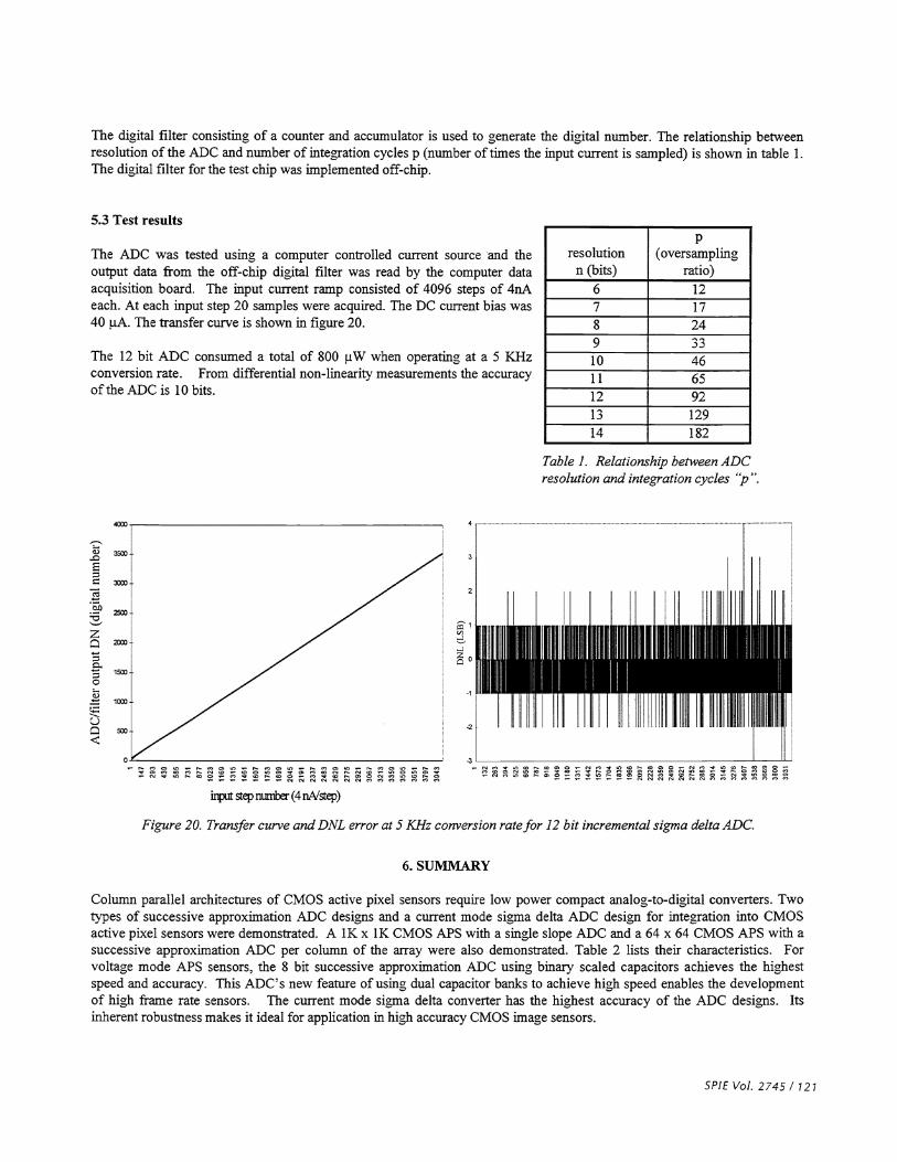
The digital filter consisting of a counter and accumulator is used to generate the digital number. The relationship betweenresolution of the ADO and number of integration cycles p (number of times the input current is sampled) is shown in table 1.The digital filter for the test chip was implemented off-chip.
5.3 Test results
The ADC was tested using a computer controlled current source and theoutput data from the off-chip digital filter was read by the computer dataacquisition board. The input current ramp consisted of 4096 steps of 4nAeach. At each input step 20 samples were acquired. The DC current bias was40 A. The transfer curve is shown in figure 20.
The 12 bit ADC consumed a total of 800 iW when operating at a 5 KHzconversion rate. From differential non-linearity measurements the accuracyof the ADC is 10 bits.
.
z
C
resolutionn (bits)
p(oversampling
ratio)6 127 178 249 3310 4611 6512 9213 12914 182
Table 1. Relationship between ADCresolution and integration cycles "p".
Figure 20. Transfer curve and DNL error at 5 K[-Izconversion ratefor 12 bit incremental sigma delta ADC.
6. SUMMARY
Column parallel architectures of CMOS active pixel sensors require low power compact analog-to-digital converters. Twotypes of successive approximation ADO designs and a current mode sigma delta ADO design for integration into CMOSactive pixel sensors were demonstrated. A 1K x 1K CMOS APS with a single slope ADC and a 64 x 64 CMOS APS with asuccessive approximation ADC per column of the array were also demonstrated. Table 2 lists their characteristics. Forvoltage mode APS sensors, the 8 bit successive approximation ADO using binary scaled capacitors achieves the highestspeed and accuracy. This ADC's new feature of using dual capacitor banks to achieve high speed enables the developmentof high frame rate sensors. The current mode sigma delta converter has the highest accuracy of the ADO designs. Itsinherent robustness makes it ideal for application in high accuracy CMOS image sensors.
SPIE Vol. 2745 I 121
inpit nnb(4nN)
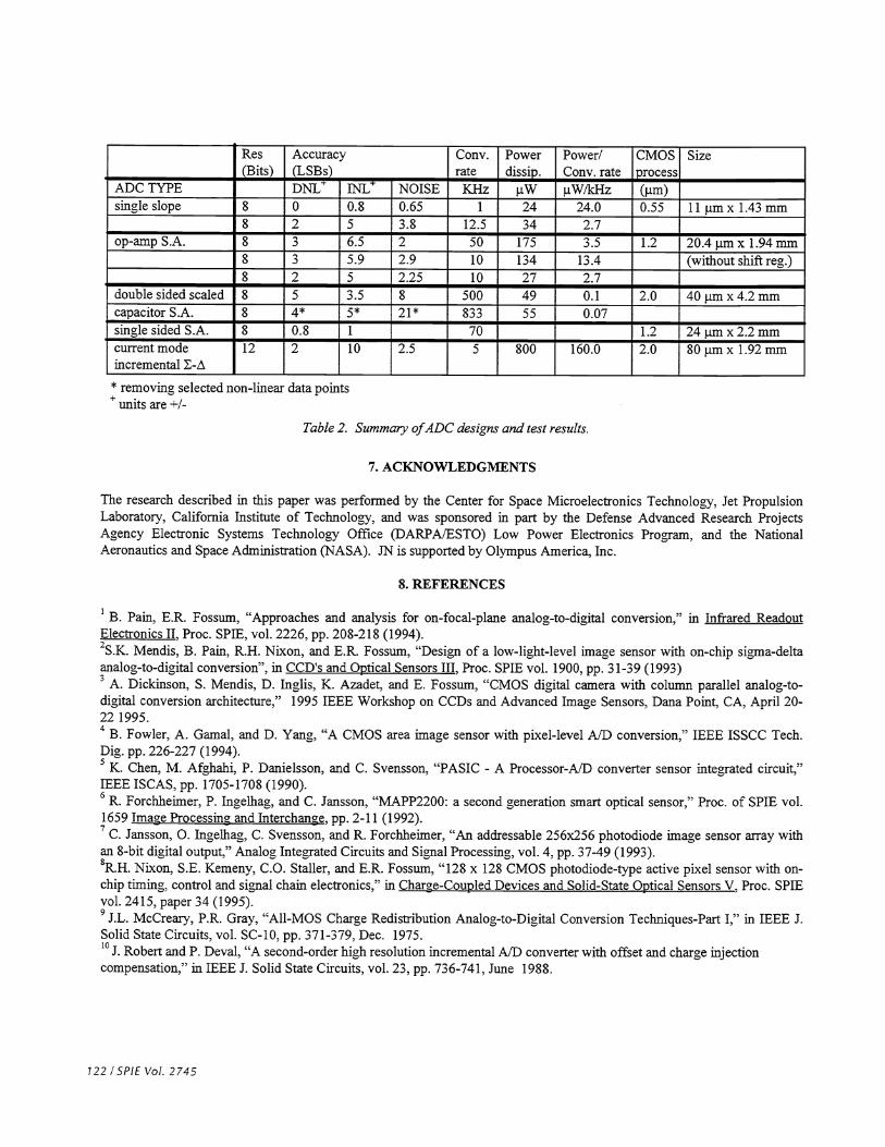
Res
(Bits)Accuracy(LSBs)
Cony.rate
Powerdissip.
Power!Cony. rate
CMOSprocess
Size
ADC TYPE DNL [NL NOISE KHz jtW iW!kHz (!tm)single slope 8 0 0.8 0.65 1 24 24.0 0.55 1 1 .tm x 1 .43 mm
8 2 5 3.8 12.5 34 2.7op-amp S.A. 8 3 6.5 2 50 175 3.5 1.2 20.4 jm x 1.94 mm
8 3 5.9 2.9 10 134 13.4 (without shift reg.)8 2 5 2.25 10 27 2.7
double sided scaled 8 5 3.5 8 500 49 0.1 2.0 40 jm x 4.2 mmcapacitorS.A. 8 4* 5* 21* 833 55 0.07single sided S.A. 8 0.8 1 70 1.2 24 pm x 2.2 mmcurrent modeincremental
12 2 10 2.5 5 800 160.0 2.0 80 pm x 1 .92 mm
* removing selected non-linear data points+
units are +1-
Table 2. Summary ofADC designs and test results.
7. ACKNOWLEDGMENTS
The research described in this paper was performed by the Center for Space Microelectronics Technology, Jet PropulsionLaboratory, California Institute of Technology, and was sponsored in part by the Defense Advanced Research ProjectsAgency Elec-onic Systems Technology Office (DARPA/ESTO) Low Power Electronics Program, and the NationalAeronautics and Space Administration (NASA). JN is supported by Olympus America, Inc.
8. REFERENCES
I B. Pain, E.R. Fossum, "Approaches and analysis for on-focal-plane analog-to-digital conversion," in Infrared ReadoutElectronics II, Proc. SPIE, vol. 2226, pp. 208-218 (1994).2S.K. Mendis, B. Pain, R.H. Nixon, and E.R. Fossum, "Design of a low-light-level image sensor with on-chip sigma-deltaanalog-to-digital conversion", in CCD's and Optical Sensors III, Proc. SPIE vol. 1900, pp. 3 1-39 (1993)-, A. Dickinson, S. Mendis, D. Inglis, K. Azadet, and E. Fossum, "CMOS digital camera with column parallel analog-to-digital conversion architecture," 1995 IEEE Workshop on CCDs and Advanced Image Sensors, Dana Point, CA, April 20-22 1995.4
B. Fowler, A. Gamal, and D. Yang, "A CMOS area image sensor with pixel-level AiD conversion," IEEE ISSCC Tech.Dig. pp. 226-227 (1994).5 K. Chen, M. Afghahi, P. Danielsson, and C. Svensson, "PASIC -A Processor-AiD converter sensor integrated circuit,"IEEE ISCAS, pp. 1705-1708 (1990).6 R. Forchheimer, P. Ingelhag, and C. Jansson, "MAPP2200: a second generation smart optical sensor," Proc. of SPIE vol.1659 Image Processing and Interchange, pp. 2-11 (1992).7 C. Jansson, 0. Ingeihag, C. Svensson, and R. Forchheimer, "An addressable 256x256 photodiode image sensor array withan 8-bit digital output," Analog Integrated Circuits and Signal Processing, vol. 4, pp. 37-49 (1993).8R.H. Nixon, S.E. Kemeny, C.O. Staller, and E.R. Fossum, "128 x 128 CMOS photodiode-type active pixel sensor with on-chip timing, control and signal chain electronics," in Charge-Coupled Devices and Solid-State Optical Sensors V, Proc. SPIEvol. 2415, paper 34 (1995).9
J.L. McCreary, P.R. Gray, "All-MOS Charge Redistribution Analog-to-Digital Conversion Techniques-Part I," in IEEE J.Solid State Circuits, vol. SC-b, pp. 371-379, Dec. 1975.10 Robert and P. Deval, "A second-orderhigh resolution incremental A/D converter with offset and charge injectioncompensation," in IEEE J. Solid State Circuits, vol. 23, pp. 736-741, June 1988.
122 ISPIE Vol. 2745