Embed Size (px)
Citation preview
ON-CHIP WIRES: SCALING AND EFFICIENCY
A DISSERTATION
SUBMITTED TO THE DEPARTMENT OF ELECTRICAL ENGINEERING
AND THE COMMITTEE ON GRADUATE STUDIES
OF STANFORD UNIVERSITY
IN PARTIAL FULFILLMENT OF THE REQUIREMENTS
FOR THE DEGREE OF
DOCTOR OF PHILOSOPHY
Ron Ho
August 2003

c
Copyright by Ron Ho 2003
All Rights Reserved
ii

I certify that I have read this dissertation and that, in my opin-
ion, it is fully adequate in scope and quality as a dissertation
for the degree of Doctor of Philosophy.
Mark A. Horowitz(Principal Adviser)
I certify that I have read this dissertation and that, in my opin-
ion, it is fully adequate in scope and quality as a dissertation
for the degree of Doctor of Philosophy.
Bruce A. Wooley
I certify that I have read this dissertation and that, in my opin-
ion, it is fully adequate in scope and quality as a dissertation
for the degree of Doctor of Philosophy.
Krishna C. Saraswat
Approved for the University Committee on Graduate Stud-
ies:
iii

iv
Abstract
Recent years have seen an increase in the importance of on-chip wires, as they have slowed
down and gates have sped up. This dissertation takes a close look at the story of wire scal-
ing. It forecasts wire and gate characteristics from the Semiconductor Industry Association
roadmap and combines them into performance metrics, showing how the ratio of wire de-
lays to gate delays scales slowly for scaled-length wires and grows rapidly for fixed-length
wires.
This duality of “fast local wires” contrasted with “slow global wires” affects how we
approach VLSI designs. First, CAD place-and-route tools must improve to keep up with
growing die complexity and more local blocks gathered on a chip. Second, modular archi-
tectures can effectively exploit the dual nature of wires, using wide global buses of high
bandwidth to offset long wire latencies.
Using such wide and long global buses can burn a great deal of power, especially if
built with traditional delay-optimal CMOS repeaters. Traditional repeaters can be sized
and spaced to save about 30% in energy for only a 10% delay penalty. Because this 30%
of energy savings is not a lot, techniques for running global wires at a reduced voltage
can be very important. These include NMOS drivers, overdrive pre-emphasis, and voltage
pre-equalization. Using these circuit techniques offers an order-of-magnitude in energy
savings for no effective slowdown. Experimental results on a 180nm testchip validate this
10x savings in energy over 10mm long on-chip buses, running at 1 token per 10 gate de-
lays. Further experimental data shows receiver input offsets under 90mV, with input offset
compensation leading to residual input uncertainties of around 15mV.
v

vi

Acknowledgements
The title page of this doctoral thesis lists my name as the single author, although that is a
deception. The ideas and concepts in the pages that follow arose from the work of many
people, and to them I owe my thanks.
Mark Horowitz has done his best to teach me how to do research these past several
years. His ability to see right through problems to solutions, his patience with recalcitrant
graduate students, and his constant and easy availability made him a wonderful advisor. I
thank him for taking me on as a graduate student so many years ago.
Bruce Wooley and Krishna Saraswat agreed to be my associate advisor and third reader,
respectively, and I appreciate their assistance and input to my research and dissertation.
Nick Bambos very graciously agreed to chair my defense committee.
The staff at Stanford has been helpful, knowledgable, and supportive, as needed. Char-
lie Orgish and Joe Little have taught me more than I can remember about computers and
how to set up a computing infrastructure. Darlene Hadding, Terry West, Deborah Harber,
Lindsay Brustin, and Taru Fisher all helped me navigate the maze of Stanford administra-
tion.
My long tenure in the research group meant that I’ve had the pleasure of working with
many of Mark’s graduate students. Ken Mai bore the brunt of my idea-bouncing, as my
most frequent collaborator, and I learned a great deal from him. I also spent time building
chips with Dan Weinlader and teaching chip-building with Gu-Yeon Wei, both enjoyable
experiences. Ken Yang, Stefanos Sidiropoulus, Jeff Solomon, Hema Kapadia, and Birdy
Amrutur all enriched my Stanford career through various projects and papers. I owe my
officemates David Harris, Evelina Yeung, and Vicky Wong special mention, for putting up
with me over the years.
vii

Although my colleages at Intel more often than not tried to convince me to “give up
that Ph.D. pipe dream and come back full-time,” I owe much to them, especially Jason
Stinson, Branko Perazich, Ron Zinger, and Mehrdad Mohebbi. Over the past ten years,
their friendship, knowledge in designing CPUs, and, of course, willingness to employ me
were all invaluable to my parallel career in graduate school. My current colleagues at
Sun, Robert Drost and Ivan Sutherland, have greatly encouraged these final steps towards
completion.
My sister Minnie and her husband Rohit both served as existence proofs for the obtain-
ability of a Stanford engineering doctorate. My parents, long before graduate school and
long before Stanford, taught me how to think and how to be curious about how and why
things worked. They started me on this path, and I’m grateful that they did.
But above all and most importantly, my wife Christina showed unflagging support,
optimism, and patience. Without her help I would never have finished this work, and so I
humbly dedicate it to her.
viii

Contents
Abstract v
Acknowledgements vii
1 Introduction 1
1.1 Organization . . . . . . . . . . . . . . . . . . . . . . . . . . . . . . . . . . 3
2 Metrics, models, and scaling 4
2.1 A simple gate delay model . . . . . . . . . . . . . . . . . . . . . . . . . . 4
2.2 Wire characteristics . . . . . . . . . . . . . . . . . . . . . . . . . . . . . . 5
2.2.1 Resistance . . . . . . . . . . . . . . . . . . . . . . . . . . . . . . 6
2.2.2 Capacitance . . . . . . . . . . . . . . . . . . . . . . . . . . . . . . 8
2.2.3 Inductance . . . . . . . . . . . . . . . . . . . . . . . . . . . . . . 10
2.3 Wire performance metrics . . . . . . . . . . . . . . . . . . . . . . . . . . 13
2.3.1 Signal coupling . . . . . . . . . . . . . . . . . . . . . . . . . . . . 13
2.3.2 Wire delay . . . . . . . . . . . . . . . . . . . . . . . . . . . . . . 17
2.3.3 Repeaters . . . . . . . . . . . . . . . . . . . . . . . . . . . . . . . 21
2.4 Gate metrics under scaling . . . . . . . . . . . . . . . . . . . . . . . . . . 22
2.5 Wire characteristics under scaling . . . . . . . . . . . . . . . . . . . . . . 24
2.5.1 Resistance under scaling . . . . . . . . . . . . . . . . . . . . . . . 26
2.5.2 Capacitance and inductance under scaling . . . . . . . . . . . . . . 26
2.5.3 Noise as a limiter to scaling . . . . . . . . . . . . . . . . . . . . . 29
2.5.4 Noise minimization techniques . . . . . . . . . . . . . . . . . . . . 29
2.6 Wire performance under scaling . . . . . . . . . . . . . . . . . . . . . . . 32
ix
2.7 Summary . . . . . . . . . . . . . . . . . . . . . . . . . . . . . . . . . . . 36
3 Implications of Scaling 37
3.1 Design at the ground level: CAD tools . . . . . . . . . . . . . . . . . . . . 38
3.1.1 Claim: CAD tools need not improve . . . . . . . . . . . . . . . . . 38
3.1.2 Underlying problem in synthesis . . . . . . . . . . . . . . . . . . . 40
3.1.3 Wire exceptions . . . . . . . . . . . . . . . . . . . . . . . . . . . . 41
3.2 Design at 50,000 feet: Architectures . . . . . . . . . . . . . . . . . . . . . 46
3.2.1 A historical perspective . . . . . . . . . . . . . . . . . . . . . . . . 47
3.2.2 On-die signal range . . . . . . . . . . . . . . . . . . . . . . . . . . 49
3.2.3 Wire-aware architectures: modularity . . . . . . . . . . . . . . . . 51
3.3 Efficient global wiring networks . . . . . . . . . . . . . . . . . . . . . . . 55
3.4 Summary . . . . . . . . . . . . . . . . . . . . . . . . . . . . . . . . . . . 56
4 Efficient Repeaters 57
4.1 Coding for energy savings . . . . . . . . . . . . . . . . . . . . . . . . . . 57
4.2 CMOS repeaters . . . . . . . . . . . . . . . . . . . . . . . . . . . . . . . . 61
4.2.1 Optimizing for delay . . . . . . . . . . . . . . . . . . . . . . . . . 61
4.2.2 Optimizing for energy-delay product . . . . . . . . . . . . . . . . . 64
4.2.3 Other constraints and metrics . . . . . . . . . . . . . . . . . . . . . 66
4.3 General repeater models . . . . . . . . . . . . . . . . . . . . . . . . . . . 68
4.3.1 Delay and energy for the general model . . . . . . . . . . . . . . . 70
4.4 Examples of repeater optimizations . . . . . . . . . . . . . . . . . . . . . . 71
4.4.1 Example: Buffers . . . . . . . . . . . . . . . . . . . . . . . . . . . 71
4.4.2 Example 2: Tristates . . . . . . . . . . . . . . . . . . . . . . . . . 74
4.5 Summary . . . . . . . . . . . . . . . . . . . . . . . . . . . . . . . . . . . 78
5 Low-Swing Repeaters 80
5.1 Benefits and costs of low-swing signaling . . . . . . . . . . . . . . . . . . 80
5.2 Low-swing repeater systems . . . . . . . . . . . . . . . . . . . . . . . . . 83
5.2.1 Low-swing transmitter circuits . . . . . . . . . . . . . . . . . . . . 83
5.2.2 Wire engineering . . . . . . . . . . . . . . . . . . . . . . . . . . . 92
x

5.2.3 Low-swing receivers . . . . . . . . . . . . . . . . . . . . . . . . . 97
5.3 Putting it all together . . . . . . . . . . . . . . . . . . . . . . . . . . . . . 104
6 Experimental Results 105
6.1 Testchip overview . . . . . . . . . . . . . . . . . . . . . . . . . . . . . . . 105
6.2 Bus experiments . . . . . . . . . . . . . . . . . . . . . . . . . . . . . . . . 108
6.2.1 Overhead . . . . . . . . . . . . . . . . . . . . . . . . . . . . . . . 109
6.2.2 Measurement circuits . . . . . . . . . . . . . . . . . . . . . . . . . 110
6.2.3 Performance and results . . . . . . . . . . . . . . . . . . . . . . . 112
6.3 Offset experiments . . . . . . . . . . . . . . . . . . . . . . . . . . . . . . 118
6.3.1 Offset measurements . . . . . . . . . . . . . . . . . . . . . . . . . 118
6.3.2 Systematic errors . . . . . . . . . . . . . . . . . . . . . . . . . . . 121
6.3.3 Residual offsets after compensation . . . . . . . . . . . . . . . . . 123
6.3.4 Offset experiments we wish we had done . . . . . . . . . . . . . . 126
6.4 Summary . . . . . . . . . . . . . . . . . . . . . . . . . . . . . . . . . . . 126
7 Conclusions 128
A Fanout in a buffered repeater 131
Bibliography 134
xi

List of Tables
2.1 Sample 12 RwireCwire delays, 0.18-µm technology . . . . . . . . . . . . . . . 19
2.2 Wire pitch dimensions for an Intel 0.18-µm technology [36] . . . . . . . . . 24
2.3 Aggressive wire predictions, technology terms only . . . . . . . . . . . . . 25
2.4 Conservative wire predictions, technology terms only . . . . . . . . . . . . 26
2.5 Resistance, in Ω/µm, with technology scaling . . . . . . . . . . . . . . . . 27
2.6 Capacitance, in fF/µm, with technology scaling . . . . . . . . . . . . . . . 28
3.1 Lcrit in gate pitches, with technology scaling . . . . . . . . . . . . . . . . . 42
3.2 Approximate FO4 per cycle for x86 Intel architectures . . . . . . . . . . . 49
4.1 Savings from using bus-invert . . . . . . . . . . . . . . . . . . . . . . . . 59
4.2 Minimal energy delay, under risetime constraints . . . . . . . . . . . . . . 68
4.3 Buffer minimal energy delay, under risetime constraints . . . . . . . . . . . 74
4.4 Minimal energy delay, under risetime constraints . . . . . . . . . . . . . . 77
5.1 Estimated improvements to receiver sizing . . . . . . . . . . . . . . . . . . 102
xii

List of Figures
1.1 The view of the future, circa 1997 . . . . . . . . . . . . . . . . . . . . . . 2
2.1 A fanout-of-four inverter delay . . . . . . . . . . . . . . . . . . . . . . . . 5
2.2 Drawn to relative scale: A 0.25-µm aluminum interconnect technology
(left) and a 0.13-µm copper interconnect technology (right) . . . . . . . . . 6
2.3 A simple resistance model . . . . . . . . . . . . . . . . . . . . . . . . . . 7
2.4 A simple capacitance model . . . . . . . . . . . . . . . . . . . . . . . . . 9
2.5 A signal wire ab and two potential returns cd and ef . . . . . . . . . . . . . 11
2.6 Partial loops for the three wires . . . . . . . . . . . . . . . . . . . . . . . . 11
2.7 Bus coupling noise model . . . . . . . . . . . . . . . . . . . . . . . . . . . 15
2.8 Decomposition of attacker and victim waveforms . . . . . . . . . . . . . . 15
2.9 Idealized wave-pipeline with 1-, 2-, and 3-τ repeat rates . . . . . . . . . . . 20
2.10 Unrepeated bandwidth, in an 0.18-µm technology . . . . . . . . . . . . . . 21
2.11 FO4 scaling at TTLH (90% Vdd, 125 degrees). . . . . . . . . . . . . . . . . 23
2.12 Resistance scaling, optimisitic and pessimistic trend curves . . . . . . . . . 27
2.13 Capacitance scaling, optimisitic and pessimistic trend curves . . . . . . . . 28
2.14 Staggering repeaters minimizes injected noise . . . . . . . . . . . . . . . . 30
2.15 Charge compensation devices inject “negative” noise . . . . . . . . . . . . 30
2.16 Twisted differential wires effectively eliminate noise . . . . . . . . . . . . 31
2.17 Two kinds of wire on a chip: local and global . . . . . . . . . . . . . . . . 32
2.18 Local unrepeated wires, spanning 800 standard cells: 10x penalty over nine
generations. The lines indicate optimistic and pessimistic scaling trends. . . 33
2.19 Global unrepeated wires, spanning 5mm: 2000x penalty over nine genera-
tions. The lines indicate optimistic and pessimistic scaling trends. . . . . . 34
xiii
2.20 Global repeated wires, spanning 5mm: 40x penalty over nine generations . 34
2.21 Local repeated wires, spanning 800 standard cells: 2-3x penalty over nine
generations . . . . . . . . . . . . . . . . . . . . . . . . . . . . . . . . . . 35
3.1 Average wire length versus gate count . . . . . . . . . . . . . . . . . . . . 39
3.2 Estimated versus actual wire loads . . . . . . . . . . . . . . . . . . . . . . 41
3.3 Lcrit scaling . . . . . . . . . . . . . . . . . . . . . . . . . . . . . . . . . . 43
3.4 M-Machine IU unit versus model (k=3, p=0.7, f=2.3) . . . . . . . . . . . . 43
3.5 Flash MAGIC node versus model (k=3, p=0.7, f=2.5) . . . . . . . . . . . . 44
3.6 Percentage of wires that exceed Lcrit under scaling. The two sets of curves
show optimistic and pessimistic technology scaling trends. . . . . . . . . . 44
3.7 Wire exceptions under scaling . . . . . . . . . . . . . . . . . . . . . . . . 45
3.8 CAD tools handling more wires must also handle longer wires . . . . . . . 46
3.9 Reachable distance per 16 FO4 clock, in mm . . . . . . . . . . . . . . . . 50
3.10 Reachable distance per 16 FO4 clock, in kλ . . . . . . . . . . . . . . . . . 51
3.11 Reachable distance on a chip under scaling . . . . . . . . . . . . . . . . . 52
3.12 Smart Memories project . . . . . . . . . . . . . . . . . . . . . . . . . . . 53
4.1 Bus-invert transmission logic . . . . . . . . . . . . . . . . . . . . . . . . . 59
4.2 Simple model using inverters . . . . . . . . . . . . . . . . . . . . . . . . . 61
4.3 Delay sensitivity (2% contours) . . . . . . . . . . . . . . . . . . . . . . . . 63
4.4 2% delay contours (solid lines) and 5% energy contours (dashed lines).
Energy increases towards the upper left direction. . . . . . . . . . . . . . . 65
4.5 2% contours for energy delay optimization . . . . . . . . . . . . . . . . . . 65
4.6 2% contours for energy delay optimization with risetime constraint . . . . . 67
4.7 General repeater model . . . . . . . . . . . . . . . . . . . . . . . . . . . . 69
4.8 Delay sensitivity (2% contours) with rise-time constraint (dashed line) . . . 73
4.9 Energy delay sensitivity (2% contours) with rise-time constraint (dashed line) 73
4.10 Simple model using tristate repeaters . . . . . . . . . . . . . . . . . . . . . 75
4.11 Delay sensitivity (4% contours) with rise-time constraint (dashed line) . . . 77
4.12 Delay Energy 4% contours with rise-time constraint (dashed line) . . . . . 78
xiv
5.1 Drive resistance versus power supply, for Vt 1
4Vdd . . . . . . . . . . . . . 81
5.2 Generic low-swing repeated wire . . . . . . . . . . . . . . . . . . . . . . . 83
5.3 Cutoff drivers. (a) Logical cutoff. (b) Self-cutoff. . . . . . . . . . . . . . . 84
5.4 Overdrive transmitter benefits . . . . . . . . . . . . . . . . . . . . . . . . . 87
5.5 (a) Simulation of wire split at receiver end and (b) Wire differential voltage
profile at t=6.4FO4 . . . . . . . . . . . . . . . . . . . . . . . . . . . . . . 88
5.6 Equalized versus non-equalized drivers . . . . . . . . . . . . . . . . . . . . 89
5.7 Transmitter, one of a pair, sized for a 0.18-µm technology . . . . . . . . . . 91
5.8 Driver resistance in a MOSIS 0.18-µm technology . . . . . . . . . . . . . . 91
5.9 A typical twist solution . . . . . . . . . . . . . . . . . . . . . . . . . . . . 93
5.10 Optimized twisting would put the twist at 70% down the wire . . . . . . . . 94
5.11 Simulated noise, 5mm wires, 100Ω and 50Ω drive resistances . . . . . . . 95
5.12 Peak of simulated noise, with optimal around 70% . . . . . . . . . . . . . 96
5.13 Receiver amplifier, in 0.18-µm technology . . . . . . . . . . . . . . . . . . 98
5.14 Sense amplifier delays . . . . . . . . . . . . . . . . . . . . . . . . . . . . 100
6.1 Chip photomicrograph . . . . . . . . . . . . . . . . . . . . . . . . . . . . 107
6.2 Master-slave variant of on-die sampler circuit, sized for a 0.18-µ technology 110
6.3 Low-swing bus at 500MHz . . . . . . . . . . . . . . . . . . . . . . . . . . 113
6.4 Low-swing bus at 1GHz . . . . . . . . . . . . . . . . . . . . . . . . . . . 114
6.5 Measured energy consumption of low-swing bus at 500MHz. Full-swing
bus had measured energy consumption of 9.84pJ/bit. . . . . . . . . . . . . 115
6.6 Measured energy consumption of low-swing bus at 1GHz. Full-swing bus
had measured energy consumption of 9.84pJ/bit. . . . . . . . . . . . . . . 116
6.7 Fully-twisted wire: no difference between “help” or “hurt” . . . . . . . . . 117
6.8 Untwisted wire: a difference between “help” and “hurt” . . . . . . . . . . . 117
6.9 Measured scan-chain disagreements. The x-axis is ∆v and the different
curves are for vcm ranging from 0.1V to 1.1V (higher vcm towards the center).119
6.10 Measured offsets versus common-mode voltage . . . . . . . . . . . . . . . 120
6.11 Measured offset of minimum channel length amplifiers . . . . . . . . . . . 120
6.12 Measured offsets in their physical locations (in volts) . . . . . . . . . . . . 121
xv

6.13 Sense amplifier . . . . . . . . . . . . . . . . . . . . . . . . . . . . . . . . 122
6.14 Residual noise error distributions . . . . . . . . . . . . . . . . . . . . . . . 124
6.15 Matching the residual noise to an error function . . . . . . . . . . . . . . . 125
6.16 Standard deviations across the entire array of amplifiers . . . . . . . . . . . 125
A.1 Delay and Energy Delay vs. buffer internal fanout . . . . . . . . . . . . . . 133
xvi

Chapter 1
Introduction
The importance of on-chip wires has dramatically risen over the past decade. Prior to the
early 1990s, chip designers could treat on-chip wires as purely capacitive loads of logic
gates; these wires had no intrinsic delays of their own. As technologies scaled into the
mid-1990s, growing wire resistance coupled with shrinking native gate speeds made wire
delays increasingly important. For example, the principal and enduring speedpath on the
PentiumPro/II/III architectures at Intel, designed in the early-to-mid 1990s, was a long
write-back bus whose wire length spanned much of the chip.
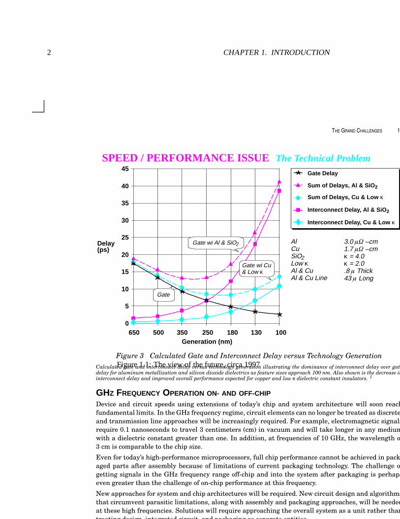
About this time, a now-famous graph projected wire and gate delays into what was
then the distant semiconductor future (see Figure 1.1). James Meindl noted wryly that this
graph, based on an early study from the 1980’s [1], should have been designated the logo
of the Semiconductor Research Corporation, so often was it invoked at industry meetings
[2]. It showed a clear divergence between gate delays and wire delays, and the use of
copper rather than aluminum only delayed the eventual cross-over. This graph raised more
questions than it answered, such as how long were the wires, what kind of gates could
run so fast, and whether speed-up technologies like repeaters were used. Regardless, it
conveyed its point clearly: like it or not, wires are getting slower as gates are getting faster.
The seemingly inexorable divergence between improving gate delays and degrading
wire delays seems to paint a bleak future for chip designers. But does it? After all, the
industry continues to produce more and more chips of enormous complexity, with designers
1
2 CHAPTER 1. INTRODUCTION
11THE GRAND CHALLENGES
THE NATIONAL TECHNOLOGY ROADMAP FOR SEMICONDUCTORS: TECHNOLOGY NEEDS
0
5
10
15
20
25
30
35
40
45
650 500 350 250 180 130 100Generation (nm)
Delay
SPEED / PERFORMANCE ISSUE The Technical Problem
AlCuSiO2Low κAl & CuAl & Cu Line
3.0 –cm1.7 –cmκ = 4.0κ = 2.0.8 Thick43 Long
Interconnect Delay, Cu & Low κ
Interconnect Delay, Al & SiO2
Sum of Delays, Cu & Low κ
Sum of Delays, Al & SiO2
Gate Delay
(ps)
Gate wi Cu& Low κ
Gate wi Al & SiO2
Gate
Figure 3 Calculated Gate and Interconnect Delay versus Technology GenerationCalculated gate and interconnect delay versus technology generation illustrating the dominance of interconnect delay over gatedelay for aluminum metallization and silicon dioxide dielectrics as feature sizes approach 100 nm. Also shown is the decrease ininterconnect delay and improved overall performance expected for copper and low κ dielectric constant insulators. 1
GHZ FREQUENCY OPERATION ON- AND OFF-CHIP
Device and circuit speeds using extensions of today’s chip and system architecture will soon reachfundamental limits. In the GHz frequency regime, circuit elements can no longer be treated as discrete,and transmission line approaches will be increasingly required. For example, electromagnetic signalsrequire 0.1 nanoseconds to travel 3 centimeters (cm) in vacuum and will take longer in any mediumwith a dielectric constant greater than one. In addition, at frequencies of 10 GHz, the wavelength of3 cm is comparable to the chip size.
Even for today’s high-performance microprocessors, full chip performance cannot be achieved in pack-aged parts after assembly because of limitations of current packaging technology. The challenge ofgetting signals in the GHz frequency range off-chip and into the system after packaging is perhapseven greater than the challenge of on-chip performance at this frequency.
New approaches for system and chip architectures will be required. New circuit design and algorithmsthat circumvent parasitic limitations, along with assembly and packaging approaches, will be neededat these high frequencies. Solutions will require approaching the overall system as a unit rather thantreating design, integrated circuit, and packaging as separate entities.
METROLOGY AND TEST
With the increasingly smaller dimensions and the need for greater purity, metrology faces majordifficulties. Of seven compelling metrology issues, no known solution exists for one need today, for two________________________________________
1. Bohr, Mark T. “Interconnect Scaling—The Real Limiter to High Performance ULSI.” Proceedings of the 1995 IEEE International ElectronDevices Meeting, 1995, pages 241–242.
Figure 1.1: The view of the future, circa 1997

1.1. ORGANIZATION 3
constantly creating new architectures and circuits for ever-increasing performance. Chip
builders, it seems, must know things that Figure 1.1 does not express.
This dissertation takes a close look at the story of wire scaling: how do wires perform
now, and how will they perform in the future? What are designers doing today and what
will they do tomorrow? As we shall see, managing wire delay as technology scales is
important, but doing so in an energy-efficient manner is just as critical.
1.1 Organization
To understand the effects of technology scaling on on-chip wires we must first decide what
wire metrics are important. Chapter 2 describes models of wire and gate delays. These
models allow us to project the wire and gate delays in future technologies. Notice that
only their relative performance matters. If gate delays and wire delays changed identically,
either dramatically or even not at all, then the overall system design would still be balanced,
and neither gates nor wires would individually limit overall performance.
Chapter 3 takes the results from Chapter 2 and looks at the implications of such scaling
trends. Although wire scaling affects the entire VLSI design space, I limit my attention
to two areas in particular: CAD tools and their ability to automate design, and computer
architectures and how they can leverage or exploit the scaled characteristics of wires. In
discussing these latter architectural implications of scaling, I will consider long on-chip
wires and how energy efficiency on these wires will become an important design constraint.
Figuring out how to drive long wires is not a new problem. A number of solutions
using optimally-repeated CMOS repeaters are well-known. However, the problem of driv-
ing these wires efficiently is rarely considered. Being stingy with delay typically means
spending extravagently in power, and repeaters with slightly sub-optimal delays can offer
potentially large energy savings. Chapter 4 examines these tradeoffs.
Tweaking repeater sizing and placement can buy only limited energy savings. Chapter
5 departs from the full-swing CMOS repeater discussion to consider low-swing circuit
architectures. It discusses design issues related to low-swing drivers, receivers, and the
wires themselves. Chapter 6 follows and gives results from testchip experiments.
Chapter 2
Metrics, models, and scaling
In order to lay a consistent foundation for the following sections, this chapter considers
how to model the delays of wires and gates. A contemporary 0.18-µm technology will pro-
vide a framework for our discussion of gate and wire delays. Gates will use a delay metric
called an FO4, which is based on feature size and described below; wires will use simple
cross-sectional-area-based models for resistance and capacitance that lead to correspond-
ingly simple wire delay metrics. These measures of gate and wire performance can help
project trends of wire delays relative to gate delays, including side effects such as noise.
As technologies scale, some wires scale in length and others do not, and we can apply our
metrics to both of these types of wires. As we shall see, the scaled-length wires do trend
with gate delays, but the fixed-length wires do not.
2.1 A simple gate delay model
Transistors are very complicated devices that can be connected in a myriad of ways, so char-
acterizing gate performance in a way that facilitates comparisons to wires initially appears
difficult. However, for reasons of productivity, CAD tool support, and robust behavior,
VLSI designers use transistors in only a very limited set of topologies; static and simple
dynamic CMOS gates dominate digital designs. As a result, metrics that characterize the
performance of these gates will suffice.
To measure gate speed, we use the delay through an inverter driving four identical
4

2.2. WIRE CHARACTERISTICS 5
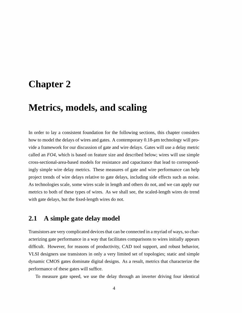
1x 4x 16x
FO4
Figure 2.1: A fanout-of-four inverter delay
copies of itself, shown in Figure 2.11. This is called a “fanout-of-four inverter delay,” or
simply an FO4. In our benchmark 0.18-µm technology, an FO4 is 90ps.
Combinational delays, composed of many different static and dynamic CMOS gate
delays, can be normalized to this FO4. The resulting relative delay holds constant over a
wide range of process technologies, temperatures, and voltages. We can therefore treat the
FO4 as our proxy for CMOS gate delays: to understand how gates compare with wires, we
need estimate the delay of only a single loaded inverter.
FO4 delays are generally constant for a given feature size; that is, one company’s
180nm technology will produce an FO4 delay reasonably close to another company’s
180nm technology. This simplifies estimating FO4s. However, specialized in-house tech-
nologies (such as those from Intel or IBM) typically offer 30-50% faster FO4 delays due
to highly optimized—and expensive—gate engineering. We will discuss this further in
Section 2.4.
2.2 Wire characteristics
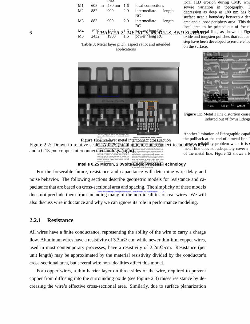
Two generations of Intel process technologies, shown as cross-sectional photographs in
Figure 2.2, reflect advances in on-chip wiring. A 0.25-µm technology from 1997, the ve-
hicle for 700MHz Pentium III processors, used five layers of aluminum metal, with shiny
tungsten plugs connecting them [3]. A 0.13-µm technology from 2002, the vehicle for
3GHz Pentium 4 processors, uses six layers of copper metal with copper vias [4]. Between
these two technologies, spanning three generations, the wires’ cross-sectional areas and
spacings fell dramatically. The importance of cross-sectional area and spacing lies in their
effects on the wire electrical characteristics that we care about: resistance and capacitance.
6 CHAPTER 2. METRICS, MODELS, AND SCALING
Intel Technology Journal Q3’98
Intel’s 0.25 Micron, 2.0Volts Logic Process Technology 5
best density. The M1 to M3 layers use tight pitch, whichis necessary for good SRAM and logic cell routingdensity. The M4 and M5 layers use wide pitch and highthickness, resulting in the low sheet rho needed for powerdistribution and cross die interconnect.
As with previous Intel processes, the metal stack is Ti/Al-Cu/Ti/TiN, which provides low line and via resistancewhile meeting electromigration requirements. Also, asbefore, the first inter-layer dielectric (ILD) above poly isBoro-Phosphosilicate-Glass (BPSG). The BPSG isplanarized using chemical-mechanical polishing (CMP).The remaining ILD layers are PTEOS oxide that use adeposition followed by an etch-back process followed byCMP planarization. The CMP steps improve layerplanarity, which is necessary for the uniform lithographicand etch processing of multi-layer interconnects.Contacts and vias are all filled with tungsten plugsformed by blanket tungsten deposition followed by CMP.
Layer Pitch Thickness
AR Purpose
M1 608 nm 480 nm 1.6 local connectionsM2 882 900 2.0 intermediate length
RCM3 882 900 2.0 intermediate length
RCM4 1520 1325 1.7 power / long RCM5 2432 1900 1.6 power / long RC
Table 3: Metal layer pitch, aspect ratio, and intendedapplications
Figure 10: Five-layer metal interconnect cross section
To achieve cost savings, most of the metal-processingtools used in P856 were used in P854. The same stepper,metal deposition, contact etcher, metal etcher, andplanarization equipment are used. A key challenge in theP856 interconnect has come from optimizing thelithographic and etch processes to work with the 20%smaller pitch of P856.
Just as Poly stretches the line width capability of DUVtools, Metal 1 patterning challenges the DUV lithographyfor space-limited capability, as the minimum spacerequired is beyond the wavelength limits. This tightpitch (608 nm) demands thin photoresist for resolution,which in turn degrades the margin for metal etch due toresist erosion. The resist erosion results in poor metalline profile (shelving) and poor metal line criticaldimension (CD) control.
Stringent control in depth of focus is also needed toensure the integrity of the lithographic patterning. Inorder to achieve a planar surface for metal lithography,CMP is used prior to metal deposition for both ILD0 andcontact plug steps. However, density variation causeslocal ILD erosion during CMP, which can result insevere variation in topography. For example, adepression as deep as 180 nm has been seen on thesurface near a boundary between a dense memory arrayarea and a loose periphery area. This depression causes alocal area to be printed out of focus and results in adistorted metal line, as shown in Figure 11. Improvedoxide and tungsten polishes that reduce the topographicalstep have been developed to ensure enough depth of focuson the surface.
Figure 11: Metal 1 line distortion caused by ILD erosioninduced out of focus lithography
Another limitation of lithographic capability is evident inthe pullback at the end of a metal line. This pullback cancause a reliability problem when it is so severe that themetal line does not adequately cover a contact at the endof the metal line. Figure 12 shows a Metal 1 void bake
Intel Technology Journal Vol. 6 Issue 2.
130nm Logic Technology Featuring 60nm Transistors, Low-K Dielectrics, and Cu Interconnects 10
Table 2: ION and IOFF at 0.7 and 1.4V VDD
In a modern microprocessor with six layers of interconnects, transistor loads are comprised of >50% interconnect capacitance. To obtain high product performance it is necessary to provide transistors with more than low CV/I; you also need high saturation and linear drive currents. Figure 6 shows the recent trend of saturation drive currents for Intel’s process technologies. This work extends the trend to offer the highest drive current to date of 1.30mA/um for low-threshold N-channel devices.
INTERCONNECTS Chip performance is increasingly limited by the RC delay of the interconnect as the transistor delay progressively decreases while the narrower lines and space actually increase the delay associated with interconnects. Using copper interconnects helps reduce this effect. This process technology uses dual damascene copper to reduce the resistances of the interconnects. Fluorinated SiO2 (FSG) is used as an inter-level dielectric (ILD) to reduce the dielectric constant; the dielectric constant k is measured to be 3.6. Figure 17 is a cross-section Scanning Electron Micrograph (SEM) image showing the dual damascene interconnects.
Aspect Ratio
(T/W) = 1.6
ILD = ILD = Fluorinated SiOFluorinated SiO22
Aspect Ratio
(T/W) = 1.6
ILD = ILD = Fluorinated SiOFluorinated SiO22
Figure 17: Cross-section SEM image of a processed wafer
Table 1 lists the metal pitches. The pitch is 350nm at the first metal layer and increases to 1200nm at the top layer. Metal aspect ratios are optimized for minimum RC delay and range from 1.6 to 2. The first metal layer uses a single damascene process, and tungsten plugs are used as contacts to the silicided regions on the silicon and poly-silicon. Unlanded contacts are supported by using an Si3N4 layer for a contact etch stop. Copper interconnects are used because of the material’s lower resistivity. The advantage is seen in Figure 18, where the sheet resistance is shown as a function of the minimum pitch of each metal layer and compared to earlier results from 180nm technologies using Al [6] and Cu [6]. The present technology exhibits 30% lower sheet resistance at the same metal pitch due to the use of Cu with high aspect ratios. The total line capacitance is 230fF/mm for M1 to M5 and slightly higher for the top layer.
DEVICE VDD IOFF (N) ION (N) ION(P) (V) (nA/um) (mA/um) (mA/um)
Low VT 1.4 100 1.30 0.66
High VT 1.4 10 1.14 0.56
Low VT 0.7 20 0.37 0.19
High VT 0.7 2 0.32 0.16
Figure 2.2: Drawn to relative scale: A 0.25-µm aluminum interconnect technology (left)and a 0.13-µm copper interconnect technology (right)
For the forseeable future, resistance and capacitance will determine wire delay and
noise behavior. The following sections describe geometric models for resistance and ca-
pacitance that are based on cross-sectional area and spacing. The simplicity of these models
does not preclude them from including many of the non-idealities of real wires. We will
also discuss wire inductance and why we can ignore its role in performance modeling.
2.2.1 Resistance
All wires have a finite conductance, representing the ability of the wire to carry a charge
flow. Aluminum wires have a resistivity of 3.3mΩ cm, while newer thin-film copper wires,
used in most contemporary processes, have a resistivity of 2.2mΩ cm. Resistance (per
unit length) may be approximated by the material resistivity divided by the conductor’s
cross-sectional area, but several wire non-idealities affect this model.
For copper wires, a thin barrier layer on three sides of the wire, required to prevent
copper from diffusing into the surrounding oxide (see Figure 2.3) raises resistance by de-
creasing the wire’s effective cross-sectional area. Similarly, due to surface planarization
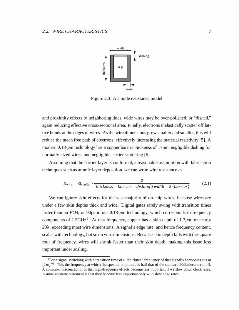
2.2. WIRE CHARACTERISTICS 7
barrier
dishing
thic
knes
s
width
α ρ.
Figure 2.3: A simple resistance model
and proximity effects to neighboring lines, wide wires may be over-polished, or “dished,”
again reducing effective cross-sectional area. Finally, electrons inelastically scatter off lat-
tice bonds at the edges of wires. As the wire dimensions grow smaller and smaller, this will
reduce the mean free path of electrons, effectively increasing the material resistivity [5]. A
modern 0.18-µm technology has a copper barrier thickness of 17nm, negligible dishing for
normally-sized wires, and negligible carrier scattering [6].
Assuming that the barrier layer is conformal, a reasonable assumption with fabrication
techniques such as atomic layer deposition, we can write wire resistance as
Rwire αscatter
ρthickness barrier dishing width 2 barrier (2.1)
We can ignore skin effects for the vast majority of on-chip wires, because wires are
under a few skin depths thick and wide. Digital gates rarely swing with transition times
faster than an FO4, or 90ps in our 0.18-µm technology, which corresponds to frequency
components of 1.5GHz1. At that frequency, copper has a skin depth of 1.7µm, or nearly
20λ, exceeding most wire dimensions. A signal’s edge rate, and hence frequency content,
scales with technology, but so do wire dimensions. Because skin depth falls with the square
root of frequency, wires will shrink faster than their skin depth, making this issue less
important under scaling.
1For a signal switching with a transition time of t, the “knee” frequency of that signal’s harmonics sits at2πt 1. This the frequency at which the spectral amplitude is half that of the standard 20db/decade rolloff.
A common misconception is that high-frequency effects become less important if we slow down clock rates.A more accurate statement is that they become less important only with slow edge rates.
8 CHAPTER 2. METRICS, MODELS, AND SCALING
At upper layers, metal widths may well exceed two skin depths, especially for those
signals carrying power or ground. Designers typically route power and ground wires right
next to each other to maximize decoupling capacitance, and by the “proximity effect,”
currents in the two wires flow as close to each other as possible, making horizontal skin
depth important. For those specialized wires, skin effects will prompt designers to break
the wide wires up into fingers.
Plugs, or vias, between aluminum metal layers were made of tungsten, and tended to be
fairly resistive; in a 0.25-µm process a M1-M2 via resistance was about 5Ω and vias from
M5 down to the substrate added up to more than 20Ω. This may seem large considering
a 1µm wide, 1mm long M5 line itself had a total resistance of only 20Ω, but by arraying
many vias together, designers could easily reduce plug resistance; in most cases, self-heat
and electromigration checks required arrayed vias for long wires anyway. Copper processes
improve via resistance by depositing vias at the same time as wires. These copper vias are
much less resistive and do not need to be as aggressively arrayed, although some recent
experience has shown that copper vias have their own electromigration concerns: they serve
as nucleation sites, gathering voids that flow down the copper wires much like tumbleweeds
[7]. Copper vias thus tend to be arrayed like aluminum vias, only for improved reliability
and not reduced resistance.
2.2.2 Capacitance
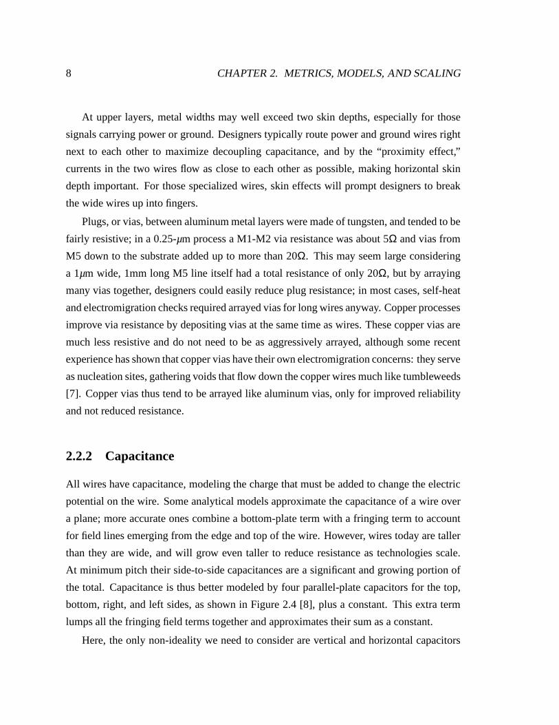
All wires have capacitance, modeling the charge that must be added to change the electric
potential on the wire. Some analytical models approximate the capacitance of a wire over
a plane; more accurate ones combine a bottom-plate term with a fringing term to account
for field lines emerging from the edge and top of the wire. However, wires today are taller
than they are wide, and will grow even taller to reduce resistance as technologies scale.
At minimum pitch their side-to-side capacitances are a significant and growing portion of
the total. Capacitance is thus better modeled by four parallel-plate capacitors for the top,
bottom, right, and left sides, as shown in Figure 2.4 [8], plus a constant. This extra term
lumps all the fringing field terms together and approximates their sum as a constant.
Here, the only non-ideality we need to consider are vertical and horizontal capacitors
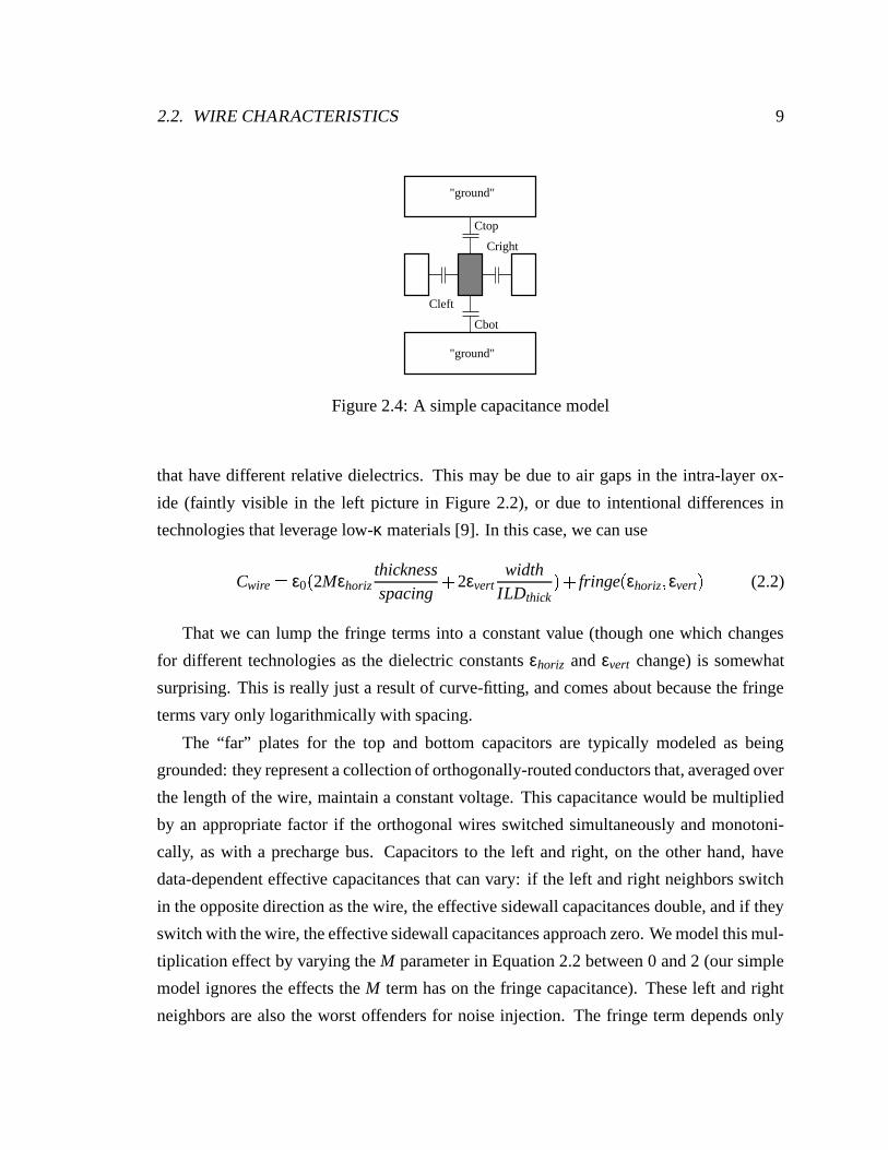
2.2. WIRE CHARACTERISTICS 9
"ground"
"ground"
Cbot
Ctop
Cright
Cleft
Figure 2.4: A simple capacitance model
that have different relative dielectrics. This may be due to air gaps in the intra-layer ox-
ide (faintly visible in the left picture in Figure 2.2), or due to intentional differences in
technologies that leverage low-κ materials [9]. In this case, we can use
Cwire ε0
2Mεhoriz
thicknessspacing
2εvert
widthILDthick
fringe
εhoriz εvert (2.2)
That we can lump the fringe terms into a constant value (though one which changes
for different technologies as the dielectric constants εhoriz and εvert change) is somewhat
surprising. This is really just a result of curve-fitting, and comes about because the fringe
terms vary only logarithmically with spacing.
The “far” plates for the top and bottom capacitors are typically modeled as being
grounded: they represent a collection of orthogonally-routed conductors that, averaged over
the length of the wire, maintain a constant voltage. This capacitance would be multiplied
by an appropriate factor if the orthogonal wires switched simultaneously and monotoni-
cally, as with a precharge bus. Capacitors to the left and right, on the other hand, have
data-dependent effective capacitances that can vary: if the left and right neighbors switch
in the opposite direction as the wire, the effective sidewall capacitances double, and if they
switch with the wire, the effective sidewall capacitances approach zero. We model this mul-
tiplication effect by varying the M parameter in Equation 2.2 between 0 and 2 (our simple
model ignores the effects the M term has on the fringe capacitance). These left and right
neighbors are also the worst offenders for noise injection. The fringe term depends only
10 CHAPTER 2. METRICS, MODELS, AND SCALING
weakly on geometry and for today’s 0.18-µm technologies with homogenous dielectrics is
about 40 fF/µm. For the very top layers of metal with no upper layers, we can use three
parallel plates with extra fringing terms on the two horizontal capacitors.
2.2.3 Inductance
All wires also have inductance, representing an inertia against changing current through
the wire. Unlike resistance or capacitance, inductance has no handy closed-form models.
Freshman physics taught us to think about the inductance of a loop, and how a changing
magnetic flux through that loop induces a voltage on it. This view of inductance does
not easily model on-chip wires, however, because we do not always know what structures
form the “loop”: if we send current down an on-chip wire, the return currents may flow
in adjacent wires, parallel power supply buses, or even the substrate. In fact, due to return
currents flowing in the paths of least impedance, the actual current loops will change with
the frequency content of the signal. At low frequencies, wide low-resistance power buses,
even if far away, have low impedance (Z R
jωL), leading to fairly large loops and hence
higher inductance. At high frequencies, far-away return paths have unattractively high
impedances, and return currents will bypass them to return in local, capacitively-coupled
wires, implying lower inductance but higher path resistance.
This “chicken-and-egg” problem is the basic challenge in calculating inductance: we
cannot know the inductance until we know what the loop (or loops) are. But we cannot
discern the correct loops until we know what the inductance is. To bypass this problem,
today’s tools define return paths to be at a fixed common reference,2 and the resultant
“partial inductances,” when combined with wire resistances and capacitances, can yield
accurate results inside circuit simulation [11][12].
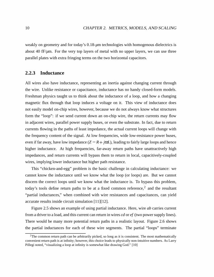
Figure 2.5 shows an example of using partial inductance. Here, wire ab carries current
from a driver to a load, and this current can return in wires cd or ef (two power supply lines).
There would be many more potential return paths in a realistic layout. Figure 2.6 shows
the partial inductances for each of these wire segments. The partial “loops” terminate
2The common return path can be arbitrarily picked, so long as it is consistent. The most mathematicallyconvenient return path is at infinity; however, this choice leads to physically non-intuitive numbers. As LarryPillegi noted, “visualizing a loop at infinity is somewhat like drawing God.” [10]
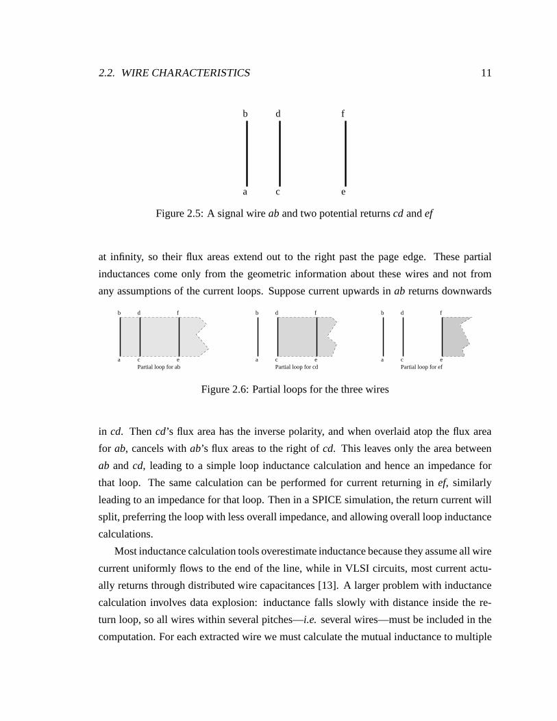
2.2. WIRE CHARACTERISTICS 11
a
b
c
d
e
f
Figure 2.5: A signal wire ab and two potential returns cd and ef
at infinity, so their flux areas extend out to the right past the page edge. These partial
inductances come only from the geometric information about these wires and not from
any assumptions of the current loops. Suppose current upwards in ab returns downwards
a
b
c
d
e
f
a
b
c
d
e
f
a
b
c
d
e
f
Partial loop for ab Partial loop for cd Partial loop for ef
Figure 2.6: Partial loops for the three wires
in cd. Then cd’s flux area has the inverse polarity, and when overlaid atop the flux area
for ab, cancels with ab’s flux areas to the right of cd. This leaves only the area between
ab and cd, leading to a simple loop inductance calculation and hence an impedance for
that loop. The same calculation can be performed for current returning in ef, similarly
leading to an impedance for that loop. Then in a SPICE simulation, the return current will
split, preferring the loop with less overall impedance, and allowing overall loop inductance
calculations.
Most inductance calculation tools overestimate inductance because they assume all wire
current uniformly flows to the end of the line, while in VLSI circuits, most current actu-
ally returns through distributed wire capacitances [13]. A larger problem with inductance
calculation involves data explosion: inductance falls slowly with distance inside the re-
turn loop, so all wires within several pitches—i.e. several wires—must be included in the
computation. For each extracted wire we must calculate the mutual inductance to multiple
12 CHAPTER 2. METRICS, MODELS, AND SCALING
neighbors, and the amount of data to store and compute quickly becomes unmanageable.
Sparsification schemes try to reduce this data without destabilizing the resultant coupling
matrices [14][15].
To determine whether or not wire inductance is important we need to consider two
questions [16][17][18]:
Does the driver-end of the wire swing slowly enough to avoid transmission-line ef-
fects? Quantitatively, does the driver impedance exceed the line impedance (Rgate
2 Z0)?
Do resistive losses in the wire outweigh any tranmission line effects? Quantitatively,
does the wire’s attenuation factor0 5 l Rwire
Z0 exceed one?
Short signal wires meet the first condition, making inductance unimportant for them. This
is because in a contemporary 0.18-µm technology, FastHenry simulations of a well-gridded
bus show Lwire 0 3nH/mm with Cwire
0 3pF/mm, making Z0 approximately 30Ω,3
much less than short-line driver resistances. Typical on-chip inductance values range from
0 2 0 5nH/mm [19]. In a 0.18-µm technology, a drive resistance less than 60Ω (twice
Z0) must be at least 85µm in width, a driver size appropriate for a 2mm-long wire. Under
scaling, both drive resistance and Z0 remain constant, maintaining this driver-impedance
inequality.
The second condition is satisfied by wires that span a typical repeater distance or longer.
As will be seen in following chapters, an optimally-repeated wire (assuming RC behavior)
has a wire length of
l 3
RgateCgate
RwireCwire(2.3)
Thus, the attenuation factor can be written
0 5 l Rwire
Z0
1 5 RwireRgateCgate Lwire
(2.4)
3We approximate Z0 LwireCwire
, while more accurately, Z0 Rwire jωLwirejωCwire
. With edge rates faster than
100ps, and hence signal frequency content exceeding 1.5GHz (10G-rad/s), this approximation holds quitewell.

2.3. WIRE PERFORMANCE METRICS 13
In our 0.18-µm technology, with Rwire 30Ω/mm and RgateCgate
10ps, the optimal re-
peater distance is about 3mm, and the attenuation term shows that line resistance over-
whelms inductance unless the wire is shorter than two-thirds the repeat distance, or 2mm.
Under scaling, the attenuation constant for a given wire will increase, making it increas-
ingly resistive.
Hence, in a 0.18-µm technology, inductance can be safely ignored for wires shorter
than 2mm and for wires longer than 2mm. For wires that are exactly 2mm long, simulations
show the delay of an LRC wire differs from the delay of an RC wire by under 3%, much less
than the uncertainty in capacitance or resistance extraction. Wire inductance is therefore
unimportant for the delay of typical signal wires.
With much wider wires having much lower resistance, such as power lines, or with
systems very sensitive to the exact delay modeling, such as clock networks, inductance
does play a role in design. For most signal wires, however, inductance effects on delay are
largely irrelevant. Inductive noise, which depends on Mδiδt, is not as easily dismissed
and will be discussed in more detail below.
2.3 Wire performance metrics
The discussion of wire characteristics above provides the groundwork for an examination of
wire performance. This section will first consider robustness by exploring signal coupling
noise issues, and then discuss delay and bandwidth metrics.
2.3.1 Signal coupling
Coupling noise is a serious problem for a chip designer, as both mutual capacitance and
inductance terms for wires can be large. To understand the magnitude of coupling noise
problems, we need to compare the induced noise to the noise margins of the receiving gate.
Static and dynamic CMOS gates are voltage controlled—they switch their output voltage
when the input voltage exceeds some threshold. Thus we are concerned about the voltage
noise on the wire relative to the voltage margins of the receiving gates.
Capacitance noise coupling is a larger effect so we will look at it first. The large aspect
14 CHAPTER 2. METRICS, MODELS, AND SCALING
ratios of modern wires mean that for a wire surrounded by neighboring wires on either
side, the cross-capacitance to these sideways neighbors dominates the total capacitance;
sideways cap can exceed 70% of the total. When these sideways neighbors (the “attackers”)
switch, the current that flows through the coupling capacitors must then flow through the
center wire (the “victim”), inducing noise on it. The familiar model of Vnoise Vswing
CcouplingCtotal
gives a pessimistic upper bound on the noise, because this is the noise voltage only if the
victim line is left floating. Many recent papers have modeled this noise more carefully,
and have shown that the noise voltage depends on both the coupling capacitance to total
capacitance ratio as well as on the ratio of the strengths of the gates driving the two wires
[21][22][23]. A convenient model simple enough for first-order hand calculations is:
Vnoise Vswing
Ccoupling
Ctotal
11
τattτvic
(2.5)
where τatt and τvic are the time constants of the attacker and victim drivers, respectively. If
the attacker has a much smaller time constant than the victim (and is hence much stronger),
the noise approaches the pessimistic worst-case. Typically, however, the transition times
of different gates are matched, which gives an attacker-to-victim time constant ratio that
is greater than one. If the two wires are identical, with identical drivers, the time constant
ratio will be set by the difference between the effective resistance of a MOS transistor in
the saturated region, driving the aggressor wire, and a transistor in the linear region, trying
to hold the value of the victim wire stable. This ratio is usually between two and four,4
which greatly reduces capacitive coupled noise for most nodes.
However, the limitation of this model is that it does not account for distributed line resis-
tance. Adding this effect makes deriving analytical results difficult, leading researchers to
use approximations like lumping the wire resistance with the driver resistance [22]. How-
ever, for the special case where the wires are identical, the most common case where cou-
pling is a problem, there is a way to view the problem using superposition that gives a
simple and intuitive view of coupling. This model starts by assuming that the driver resis-
tances are the same, as shown in Figure 2.7.
4The ratio hinges on the degree of velocity saturation of the attacking transistor. Since nMOS gates suffermore from velocity saturation, the ratio for nMOS gates is generally closer to 4.
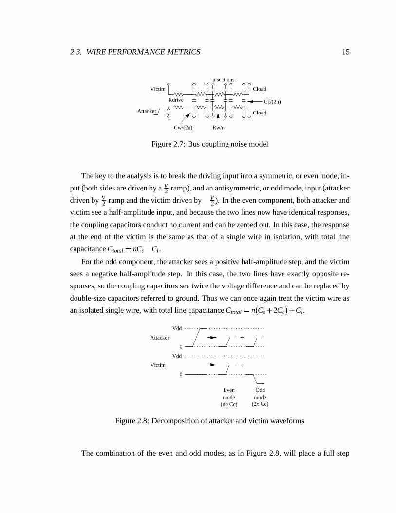
2.3. WIRE PERFORMANCE METRICS 15
Attacker
Victim
Rdrive
Cload
Cload
Cw/(2n)
n sections
Cc/(2n)
Rw/n
Figure 2.7: Bus coupling noise model
The key to the analysis is to break the driving input into a symmetric, or even mode, in-
put (both sides are driven by a V2 ramp), and an antisymmetric, or odd mode, input (attacker
driven by V2 ramp and the victim driven by V
2 ). In the even component, both attacker and
victim see a half-amplitude input, and because the two lines now have identical responses,
the coupling capacitors conduct no current and can be zeroed out. In this case, the response
at the end of the victim is the same as that of a single wire in isolation, with total line
capacitance Ctotal nCs
Cl .
For the odd component, the attacker sees a positive half-amplitude step, and the victim
sees a negative half-amplitude step. In this case, the two lines have exactly opposite re-
sponses, so the coupling capacitors see twice the voltage difference and can be replaced by
double-size capacitors referred to ground. Thus we can once again treat the victim wire as
an isolated single wire, with total line capacitance Ctotal n
Cs
2Cc
Cl.
Oddmode
(2x Cc)(no Cc)
Evenmode
0
0
Vdd
Vdd
Victim
Attacker
Figure 2.8: Decomposition of attacker and victim waveforms
The combination of the even and odd modes, as in Figure 2.8, will place a full step
16 CHAPTER 2. METRICS, MODELS, AND SCALING
on the attacker driver and hold the victim driver to ground, so we need add only the two
decoupled responses to get the true victim waveform. In other words, the victim response
can be written as the sum of two isolated wire responses, one with no coupling, and the
other with double coupling. These two isolated responses can be derived from a number
of models, ranging from simple single time-constant exponentials to more complicated
moment-matched asymptotic waveforms [24]. The key idea is that symmetry properties
allow us to break the highly-coupled circuit into two isolated circuits that are more easily
handled.
Note that this model requires that the attacker and victim lines have completely iden-
tical resistances and capacitances; in particular, we need them to have the same driver
resistances. Yet the driver of the victim wire, a transistor in its linear mode, typically has a
lower (stronger) resistance than the saturated transistor driving the attacker wire.
We avoid this limitation by observing that a driving resistor that sees a step input can
be transformed into a larger (weaker) resistor by using a slower exponential input. In
other words, from the perspective of the downstream wire, a properly-chosen exponential
input driven into a resistor is almost indistinguishable from a step input driven into a larger
(weaker) resistor. Thus if we use an appropriate exponential input instead of a step input,
and the smaller (stronger) victim resistance for both of the wire models, we will effectively
increase the attacker driving resistance while maintaining the proper victim resistance.
The mathematical derivation using simple single-time constant models for the wire
responses reduces to a peak noise given by:5
Vpeaknoise
Ccoupling
Ctotal 1
M
k
M k Mk 1
(2.6)
M nRwire
2Ratt(2.7)
where k is the ratio of attacker to victim driving resistances (typically between two and
four). For reasonable wire lengths, the driver resistance ratio does a good job of attenuating
the noise pulse, making it a small issue for static CMOS circuits. However, capacitance
coupling is a large problem for weakly-driven nodes, and CAD tools must be used to check
5Note that this formula reduces to a slightly different result than Equation 2.5 when the wire resistance is0 (i.e. when M 0). In these cases, this equation gives a better result.
2.3. WIRE PERFORMANCE METRICS 17
for coupling on such weakly-driven or dynamic nodes.
Noise from inductive coupling can also present problems for VLSI wires. The current
flowing down the aggressor wire generates a magnetic field which causes a backwards re-
turn current to flow in the victim wire. Inductive coupling pushes the victim in the opposite
direction from capacitive coupling: a rising attacker capacitively couples a victim up, but
inductively couples the victim down. While capacitive coupling is mostly a “nearest neigh-
bor” phenomenon, inductive coupling has a much larger range. Inductive noise becomes a
problem only when a large number of wires switch at the same time in bus-like situations
[25][26][27]. The worst-case noise vector would have multiple wires switching, with near
neighbors switching in one direction, and far neighbors switching in the opposite direction.
This causes the capacitive and inductive noises to add, and the accumulated noise can be
enough to cause failures [26].
Designers cope with inductive coupling by adding power planes or densely gridded
power supplies to reduce the number of wires that can couple into a victim. Power planes,
or dense power grids, effectively reduce both self and mutual inductances for wires in the
direction of the grid, because they provide very nice return paths within a few microns of
the wire itself and thus limit the extent of the magnetic coupling [28]. Most companies
have design rules for buses, such as requiring every fifth wire to be a power supply wire,
which makes inductive noise much less than capacitive noise and under 5% of the power
supply.
2.3.2 Wire delay
The delay of an on-chip wire can be modeled by a simple RC formulation. Here, we treat
a CMOS driver as a simple resistor Rgate with a parasitic load Cdiff . The CMOS receiver at
the other end of the wire presents a capacitive load Cgate.
Delay ∝ RgateCdiff
Cwire
Cgate
Rwire 12
Cwire
Cgate (2.8)
By approximating the CMOS driver with a simple resistor, this model ignores both
non-linear drive resistance as well as the effect of slew rate on delay.
This model takes advantage of the small effects inductance has on delay: it includes
18 CHAPTER 2. METRICS, MODELS, AND SCALING
only R and C terms. Inductance can affect wire delay in four ways, but all are insignificant.
First, signal propagation is limited by the speed of light down the wire, set by LC. When
the driver end of the wire switches, the receiver end cannot begin to transition until at least
l LC. This effect is insignificant: as discussed previously, wires long enough to make this
propagation delay important also have wire resistance that swamps out wire inductance.
Second, dramatically under-damped systems will ring, making single-time-constant mod-
els poor predictors of delay. But keeping driver fanouts reasonable (i.e. not smaller than
unity) prevents wires from ringing and keeps the “sharpening” effect of inductance to a
small percentage of total line delay. Third, inductive coupling, much like capacitive cou-
pling, can push out delay by forcing a victim to absorb induced transients before swinging.
With adherence to some inexpensive design heuristics, however, inductive coupling can be
made trivial in comparison to capacitive coupling. Fourth, loop inductance can force re-
turn currents into tighter loops with higher resistivity than wider loops. This extra “return
path resistance,” often overlooked by designers, is typically modeled by simply increasing
the Rwire term. This model is imperfect because the return path resistance term actually
appears after the load capacitor, so the increase in Rwire is typically done with a correction
factor that has been curve-fit to match accurate delay simulations of wiring templates. This
scheme, though somewhat inaccurate, has the virtue of easily fitting into standard CAD
timing flows.
The first term in Equation 2.8 is about 1FO4, as simple sizing heuristics aim for gate
sizes to have a fanout of about four for optimal delay [73]. Long wires with large capacitive
load might thus imply huge gates, but designers typically use higher fanouts for such long
wires; because wire resistance shields downstream capacitance from the drivers, higher
fanouts are more efficient. In these long wire cases, the 1FO4 approximation is somewhat
optimistic. We will also assume that our wires are fairly long, so that Cwire Cgate. Our
metric for delay is therefore simply 1FO4 1
2RwireCwire. These assumptions do not hold
for wires driving large or many gate loads, such as repeated wires (which we will consider
later) or control wires driving each bit of a wide datapath. Representative delay numbers
for a 0.18-µm technology are shown in Table 2.1; this table uses a total capacitance whose
cross-capacitance term is Miller-multiplied by a factor of two, to simulate a data-dependent
worst-case delay.
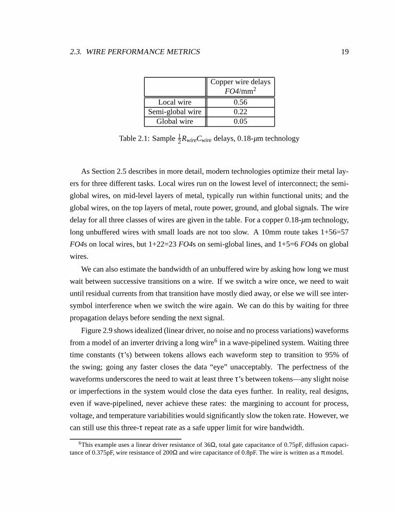
2.3. WIRE PERFORMANCE METRICS 19
Copper wire delaysFO4/mm2
Local wire 0.56Semi-global wire 0.22
Global wire 0.05
Table 2.1: Sample 12 RwireCwire delays, 0.18-µm technology
As Section 2.5 describes in more detail, modern technologies optimize their metal lay-
ers for three different tasks. Local wires run on the lowest level of interconnect; the semi-
global wires, on mid-level layers of metal, typically run within functional units; and the
global wires, on the top layers of metal, route power, ground, and global signals. The wire
delay for all three classes of wires are given in the table. For a copper 0.18-µm technology,
long unbuffered wires with small loads are not too slow. A 10mm route takes 1+56=57
FO4s on local wires, but 1+22=23 FO4s on semi-global lines, and 1+5=6 FO4s on global
wires.
We can also estimate the bandwidth of an unbuffered wire by asking how long we must
wait between successive transitions on a wire. If we switch a wire once, we need to wait
until residual currents from that transition have mostly died away, or else we will see inter-
symbol interference when we switch the wire again. We can do this by waiting for three
propagation delays before sending the next signal.
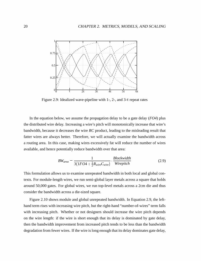
Figure 2.9 shows idealized (linear driver, no noise and no process variations) waveforms
from a model of an inverter driving a long wire6 in a wave-pipelined system. Waiting three
time constants (τ’s) between tokens allows each waveform step to transition to 95% of
the swing; going any faster closes the data “eye” unacceptably. The perfectness of the
waveforms underscores the need to wait at least three τ’s between tokens—any slight noise
or imperfections in the system would close the data eyes further. In reality, real designs,
even if wave-pipelined, never achieve these rates: the margining to account for process,
voltage, and temperature variabilities would significantly slow the token rate. However, we
can still use this three-τ repeat rate as a safe upper limit for wire bandwidth.
6This example uses a linear driver resistance of 36Ω, total gate capacitance of 0.75pF, diffusion capaci-tance of 0.375pF, wire resistance of 200Ω and wire capacitance of 0.8pF. The wire is written as a π model.
20 CHAPTER 2. METRICS, MODELS, AND SCALING
6τ5τ4τ3τ2ττ0
1
0.75
0.5
0.25
0
Figure 2.9: Idealized wave-pipeline with 1-, 2-, and 3-τ repeat rates
In the equation below, we assume the propagation delay to be a gate delay (FO4) plus
the distributed wire delay. Increasing a wire’s pitch will monotonically increase that wire’s
bandwidth, because it decreases the wire RC product, leading to the misleading result that
fatter wires are always better. Therefore, we will actually examine the bandwidth across
a routing area. In this case, making wires excessively fat will reduce the number of wires
available, and hence potentially reduce bandwidth over that area:
BWarea
1
31FO4
12 RwireCwire
BlockwidthWirepitch
(2.9)
This formulation allows us to examine unrepeated bandwidth in both local and global con-
texts. For module-length wires, we run semi-global layer metals across a square that holds
around 50,000 gates. For global wires, we run top-level metals across a 2cm die and thus
consider the bandwidth across a die-sized square.
Figure 2.10 shows module and global unrepeated bandwidth. In Equation 2.9, the left-
hand term rises with increasing wire pitch, but the right-hand “number-of-wires” term falls
with increasing pitch. Whether or not designers should increase the wire pitch depends
on the wire length: if the wire is short enough that its delay is dominated by gate delay,
then the bandwidth improvement from increased pitch tends to be less than the bandwidth
degradation from fewer wires. If the wire is long enough that its delay dominates gate delay,
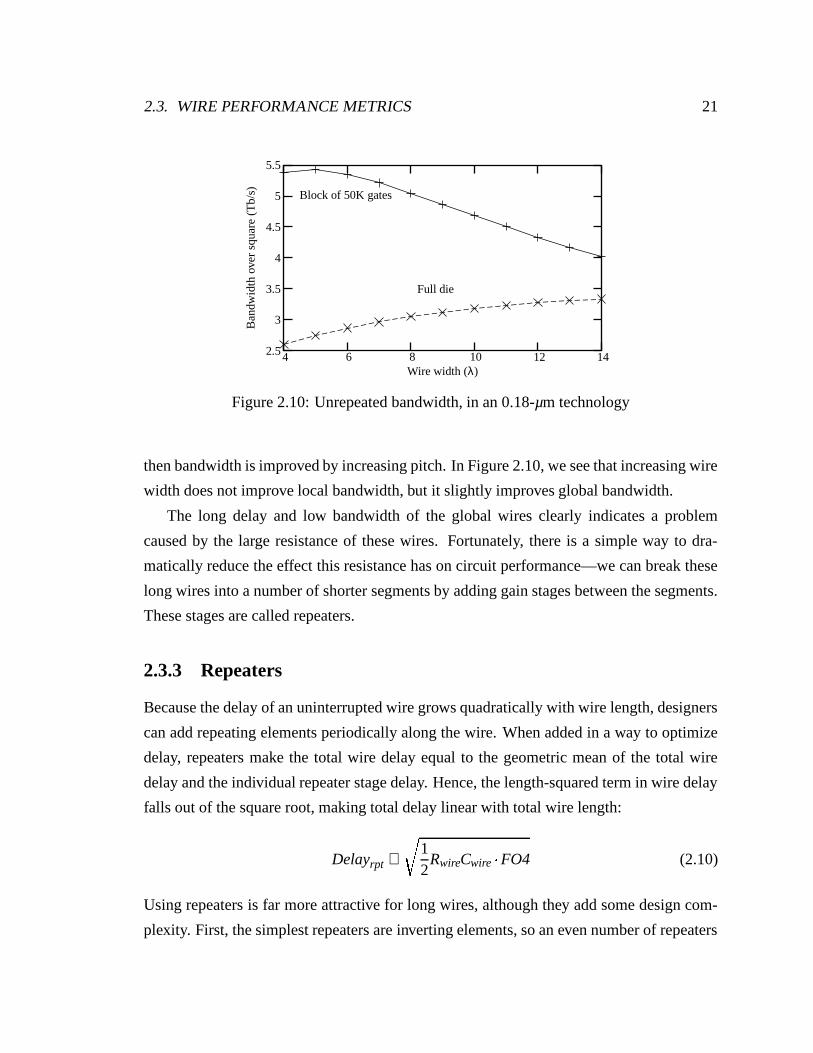
2.3. WIRE PERFORMANCE METRICS 21
Full die
Block of 50K gates
Wire width (λ)
Ban
dwid
thov
ersq
uare
(Tb/
s)
141210864
5.5
5
4.5
4
3.5
3
2.5
Figure 2.10: Unrepeated bandwidth, in an 0.18-µm technology
then bandwidth is improved by increasing pitch. In Figure 2.10, we see that increasing wire
width does not improve local bandwidth, but it slightly improves global bandwidth.
The long delay and low bandwidth of the global wires clearly indicates a problem
caused by the large resistance of these wires. Fortunately, there is a simple way to dra-
matically reduce the effect this resistance has on circuit performance—we can break these
long wires into a number of shorter segments by adding gain stages between the segments.
These stages are called repeaters.
2.3.3 Repeaters
Because the delay of an uninterrupted wire grows quadratically with wire length, designers
can add repeating elements periodically along the wire. When added in a way to optimize
delay, repeaters make the total wire delay equal to the geometric mean of the total wire
delay and the individual repeater stage delay. Hence, the length-squared term in wire delay
falls out of the square root, making total delay linear with total wire length:
Delayrpt ∝
12
RwireCwire FO4 (2.10)
Using repeaters is far more attractive for long wires, although they add some design com-
plexity. First, the simplest repeaters are inverting elements, so an even number of repeaters
22 CHAPTER 2. METRICS, MODELS, AND SCALING
is necessary to maintain logic levels7. Second, repeaters for global wires require many via
cuts from the upper-layer wires all the way down to the substrate, potentially congesting
routes on intervening layers. Third, designers are rarely afforded the luxury of placing
repeaters in their optimal locations, because they require active area; designers usually
floorplan repeaters in pre-planned clusters. Finally, even with delay-power optimizations,
repeaters are still large devices, and repeating an entire bus takes an impressive amount
of silicon area. Fortunately for these last two complications, delay and capacitance curves
for repeater insertion have fairly shallow optimizations, so that adding or removing a sin-
gle repeater stage, moving repeaters back and forth, or resizing repeaters have fairly small
costs.
Repeated wires offer substantially increased performance. After sending one signal
down a wire, we need wait only until that signal fully transitions on the first repeater seg-
ment before we send the next signal; the bandwidth of a repeated wire does not depend
on the entire wire length. Also, increasing wire pitch makes the repeated segment length
longer but does not change the segment delay, so wider wires simply reduce the number of
available routing tracks and hence do not improve bandwidth.
In Chapter 4 we will examine repeater sizing, placement, and bandwidth more closely.
For now we merely note that repeaters offer an alternative wire design structure that is
far more attractive than uninterrupted wires for long wire lengths. For either unrepeated or
repeated wires, simple geometric models for wire resistance and capacitance, when coupled
with gate delay lead directly to useful wire delay metrics. Next, we consider how these
metrics will scale with technology, beginning with gates.
2.4 Gate metrics under scaling
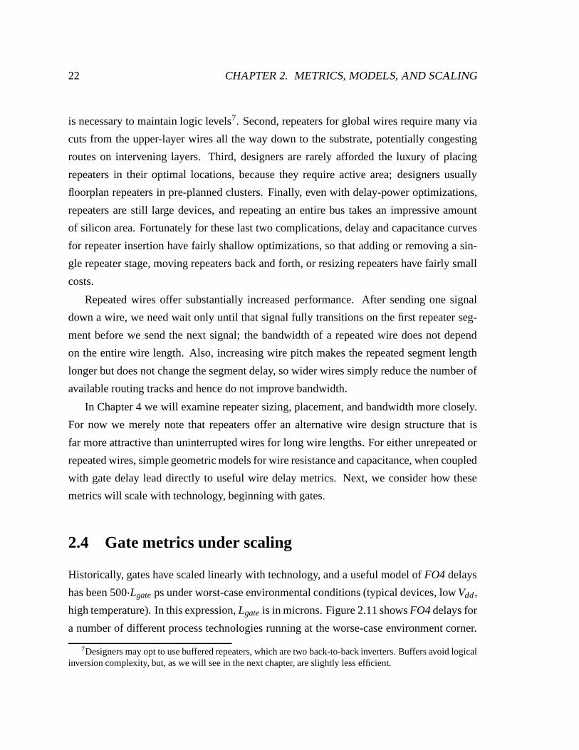
Historically, gates have scaled linearly with technology, and a useful model of FO4 delays
has been 500 Lgate ps under worst-case environmental conditions (typical devices, low Vdd ,
high temperature). In this expression, Lgate is in microns. Figure 2.11 shows FO4 delays for
a number of different process technologies running at the worse-case environment corner.
7Designers may opt to use buffered repeaters, which are two back-to-back inverters. Buffers avoid logicalinversion complexity, but, as we will see in the next chapter, are slightly less efficient.
2.4. GATE METRICS UNDER SCALING 23
This trend may continue for future generations of transistors, as devices seem scalable
down to drawn dimensions of 0.018 µm [29]. Whether or not such devices will continue to
obey the above delay model is uncertain, due to issues in scaling gate oxide, Vdd and Vth.
These concerns mean 500 Lgate ps is a lower limit for future FO4 delays. Because we are
considering wire delays relative to gate delays, faster gates provide the worst case for wire
issues, and thus we will use this model as our gate delay projection.
500ps * Lgate
Technology Ldrawn (µm)
Gat
ede
lay
(ps)
1.2 1 0.8 0.6 0.4 0.2
700
600
500
400
300
200
100
0
Figure 2.11: FO4 scaling at TTLH (90% Vdd, 125 degrees).
In a commodity 0.18-µm technology, our model accurately predicts FO4 to be about
90ps. In advanced in-house foundries, such as Intel’s, FO4s are considerably faster: due to
notches in the poly gates, the physical gate length Lgate ends up quite a bit smaller than the
drawn (and advertised) feature size.8 For example, Intel’s 0.18-µm gates have a physical
gate length of slightly under 100nm [20], and Intel’s 0.13-µm gates have a physical gate
length of 65nm [4]. Our model still holds as long as we use the correct physical gate length,
so an FO4 in the Intel 0.18-µm process is about 50ps. This gap between commodity and
advanced transistor technologies appears to be a fairly constant 2x multiplier, allowing us
to continue to use our scaling formula.
We assume that other device parameters, such as gate and diffusion capacitance, will
also continue to scale. Gate capacitance (per unit width) will remain around 1.5-2 fF/µm;
8This is not the same as simply saying that “electrical gate length is shorter than drawn gate length,”because it is a physical modification of the gate length.

24 CHAPTER 2. METRICS, MODELS, AND SCALING
although this would seem to demand too-thin gate oxides, high-κ dielectrics may permit
this aggressive scaling of the effective Tox [30]. We project diffusion capacitance to stay
at about half the gate capacitance for legged devices, although trench technologies and/or
SOI can reduce this [31].
2.5 Wire characteristics under scaling
Before we look at how wire characteristics will scale, we will first examine the geometry
assumptions in our baseline 0.18-µm technology. This process has multiple layers of copper
interconnect, with upper layers wider and taller than lower ones. The lowest metal layer,
M1, has the finest pitch and hence the highest resistance, and it predominantly connects
nets within gates or between relatively close gates. The middle layers, M2 through M4,
have a wider pitch than M1 and connect both short- and long-haul routes, typically within
functional units. The top layers, M5 and M6, have the widest pitch and hence the lowest
resistance and they usually carry global routes, power and ground, and clock. Table 2.2
shows the pitches for these various layers in a contemporary 0.18-µm technology. The
pitches are described in technology-independent λ’s, where a λ is half of the drawn gate
length. We will use similar wire pitches in our scaled technology projections: for our
purposes, local wires have a pitch of 5λ, semi-global wires a pitch of 8λ, and global wires
a pitch of 16λ.
Metal Pitch, µm Pitch, λM6 1.76 20M5 1.6 18M4 1.08 12M3 0.64 7M2 0.64 7M1 0.5 5.5
Table 2.2: Wire pitch dimensions for an Intel 0.18-µm technology [36]
Predicting the future of wire technologies is tricky; whatever we say will almost cer-
tainly turn out to be wrong. Hence, we take a two-sided approach in this section. First, we
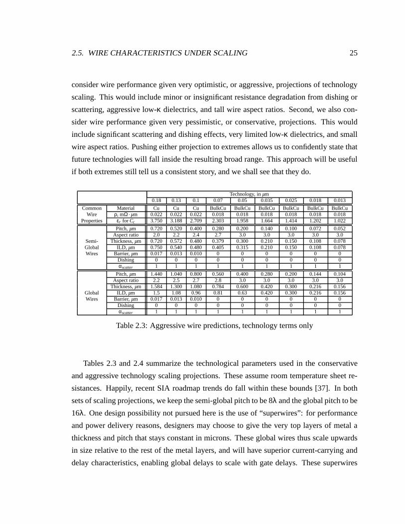
2.5. WIRE CHARACTERISTICS UNDER SCALING 25
consider wire performance given very optimistic, or aggressive, projections of technology
scaling. This would include minor or insignificant resistance degradation from dishing or
scattering, aggressive low-κ dielectrics, and tall wire aspect ratios. Second, we also con-
sider wire performance given very pessimistic, or conservative, projections. This would
include significant scattering and dishing effects, very limited low-κ dielectrics, and small
wire aspect ratios. Pushing either projection to extremes allows us to confidently state that
future technologies will fall inside the resulting broad range. This approach will be useful
if both extremes still tell us a consistent story, and we shall see that they do.
Technology, in µm0.18 0.13 0.1 0.07 0.05 0.035 0.025 0.018 0.013
Common Material Cu Cu Cu BulkCu BulkCu BulkCu BulkCu BulkCu BulkCuWire ρ, mΩ µm 0.022 0.022 0.022 0.018 0.018 0.018 0.018 0.018 0.018
Properties εr for Cc 3.750 3.188 2.709 2.303 1.958 1.664 1.414 1.202 1.022
Pitch, µm 0.720 0.520 0.400 0.280 0.200 0.140 0.100 0.072 0.052Aspect ratio 2.0 2.2 2.4 2.7 3.0 3.0 3.0 3.0 3.0
Semi- Thickness, µm 0.720 0.572 0.480 0.379 0.300 0.210 0.150 0.108 0.078Global ILD, µm 0.750 0.540 0.480 0.405 0.315 0.210 0.150 0.108 0.078Wires Barrier, µm 0.017 0.013 0.010 0 0 0 0 0 0
Dishing 0 0 0 0 0 0 0 0 0αscatter 1 1 1 1 1 1 1 1 1
Pitch, µm 1.440 1.040 0.800 0.560 0.400 0.280 0.200 0.144 0.104Aspect ratio 2.2 2.5 2.7 2.8 3.0 3.0 3.0 3.0 3.0
Thickness, µm 1.584 1.300 1.080 0.784 0.600 0.420 0.300 0.216 0.156Global ILD, µm 1.5 1.08 0.96 0.81 0.63 0.420 0.300 0.216 0.156Wires Barrier, µm 0.017 0.013 0.010 0 0 0 0 0 0
Dishing 0 0 0 0 0 0 0 0 0αscatter 1 1 1 1 1 1 1 1 1
Table 2.3: Aggressive wire predictions, technology terms only
Tables 2.3 and 2.4 summarize the technological parameters used in the conservative
and aggressive technology scaling projections. These assume room temperature sheet re-
sistances. Happily, recent SIA roadmap trends do fall within these bounds [37]. In both
sets of scaling projections, we keep the semi-global pitch to be 8λ and the global pitch to be
16λ. One design possibility not pursued here is the use of “superwires”: for performance
and power delivery reasons, designers may choose to give the very top layers of metal a
thickness and pitch that stays constant in microns. These global wires thus scale upwards
in size relative to the rest of the metal layers, and will have superior current-carrying and
delay characteristics, enabling global delays to scale with gate delays. These superwires
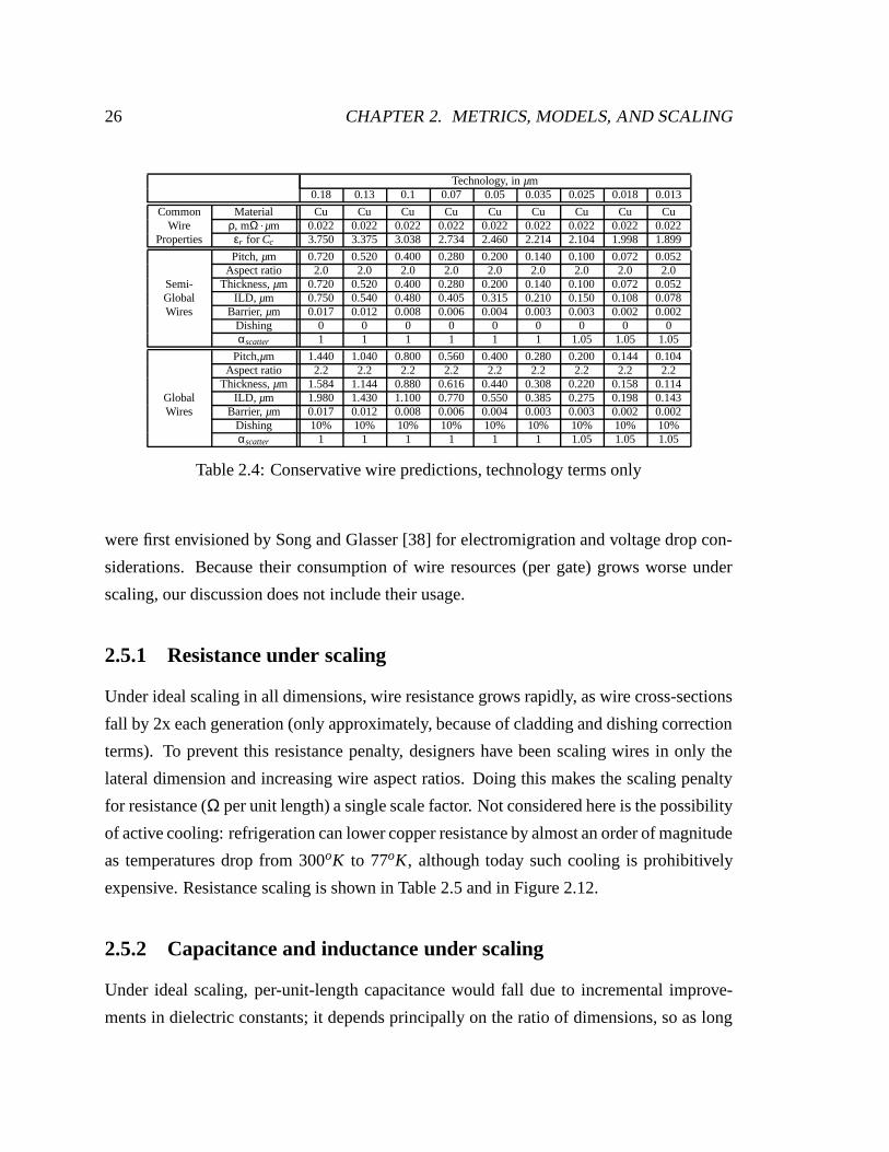
26 CHAPTER 2. METRICS, MODELS, AND SCALING
Technology, in µm0.18 0.13 0.1 0.07 0.05 0.035 0.025 0.018 0.013
Common Material Cu Cu Cu Cu Cu Cu Cu Cu CuWire ρ, mΩ µm 0.022 0.022 0.022 0.022 0.022 0.022 0.022 0.022 0.022
Properties εr for Cc 3.750 3.375 3.038 2.734 2.460 2.214 2.104 1.998 1.899
Pitch, µm 0.720 0.520 0.400 0.280 0.200 0.140 0.100 0.072 0.052Aspect ratio 2.0 2.0 2.0 2.0 2.0 2.0 2.0 2.0 2.0
Semi- Thickness, µm 0.720 0.520 0.400 0.280 0.200 0.140 0.100 0.072 0.052Global ILD, µm 0.750 0.540 0.480 0.405 0.315 0.210 0.150 0.108 0.078Wires Barrier, µm 0.017 0.012 0.008 0.006 0.004 0.003 0.003 0.002 0.002
Dishing 0 0 0 0 0 0 0 0 0αscatter 1 1 1 1 1 1 1.05 1.05 1.05
Pitch,µm 1.440 1.040 0.800 0.560 0.400 0.280 0.200 0.144 0.104Aspect ratio 2.2 2.2 2.2 2.2 2.2 2.2 2.2 2.2 2.2
Thickness, µm 1.584 1.144 0.880 0.616 0.440 0.308 0.220 0.158 0.114Global ILD, µm 1.980 1.430 1.100 0.770 0.550 0.385 0.275 0.198 0.143Wires Barrier, µm 0.017 0.012 0.008 0.006 0.004 0.003 0.003 0.002 0.002
Dishing 10% 10% 10% 10% 10% 10% 10% 10% 10%αscatter 1 1 1 1 1 1 1.05 1.05 1.05
Table 2.4: Conservative wire predictions, technology terms only
were first envisioned by Song and Glasser [38] for electromigration and voltage drop con-
siderations. Because their consumption of wire resources (per gate) grows worse under
scaling, our discussion does not include their usage.
2.5.1 Resistance under scaling
Under ideal scaling in all dimensions, wire resistance grows rapidly, as wire cross-sections
fall by 2x each generation (only approximately, because of cladding and dishing correction
terms). To prevent this resistance penalty, designers have been scaling wires in only the
lateral dimension and increasing wire aspect ratios. Doing this makes the scaling penalty
for resistance (Ω per unit length) a single scale factor. Not considered here is the possibility
of active cooling: refrigeration can lower copper resistance by almost an order of magnitude
as temperatures drop from 300oK to 77oK, although today such cooling is prohibitively
expensive. Resistance scaling is shown in Table 2.5 and in Figure 2.12.
2.5.2 Capacitance and inductance under scaling
Under ideal scaling, per-unit-length capacitance would fall due to incremental improve-
ments in dielectric constants; it depends principally on the ratio of dimensions, so as long

2.5. WIRE CHARACTERISTICS UNDER SCALING 27
Technology, in µm0.18 0.13 0.1 0.07 0.05 0.035 0.025 0.018 0.013
Aggr. semi-global wires 0.096 0.168 0.260 0.340 0.600 1.224 2.400 4.630 8.876Aggr. global wires 0.020 0.035 0.054 0.082 0.150 0.306 0.600 1.157 2.219
Cons. semi-global wires 0.096 0.184 0.307 0.627 1.220 2.509 5.014 9.821 19.458Cons. global wires 0.023 0.044 0.073 0.150 0.292 0.598 1.183 2.298 4.474
Table 2.5: Resistance, in Ω/µm, with technology scaling
Global wires
Semi-global wires
Technology Ldrawn (µm)
Res
ista
nce
(Ω/µ
m)
0.0130.0180.0250.0350.050.070.10.130.18
100
10
1
0.1
0.01
Figure 2.12: Resistance scaling, optimisitic and pessimistic trend curves
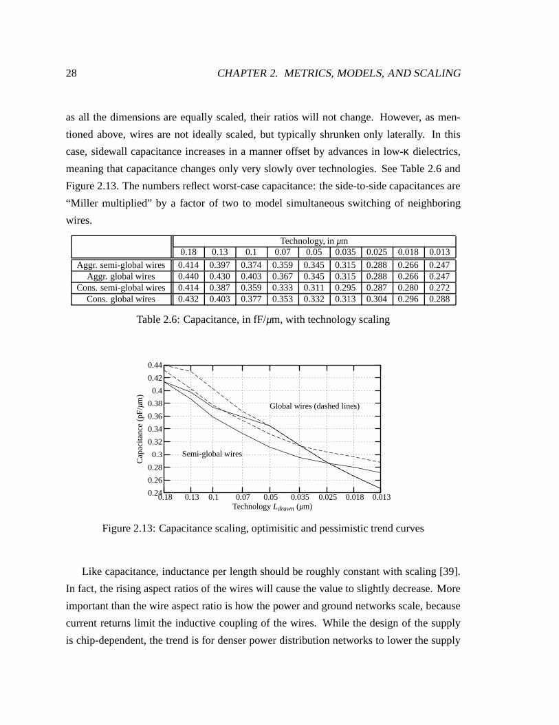
28 CHAPTER 2. METRICS, MODELS, AND SCALING
as all the dimensions are equally scaled, their ratios will not change. However, as men-
tioned above, wires are not ideally scaled, but typically shrunken only laterally. In this
case, sidewall capacitance increases in a manner offset by advances in low-κ dielectrics,
meaning that capacitance changes only very slowly over technologies. See Table 2.6 and
Figure 2.13. The numbers reflect worst-case capacitance: the side-to-side capacitances are
“Miller multiplied” by a factor of two to model simultaneous switching of neighboring
wires.
Technology, in µm0.18 0.13 0.1 0.07 0.05 0.035 0.025 0.018 0.013
Aggr. semi-global wires 0.414 0.397 0.374 0.359 0.345 0.315 0.288 0.266 0.247Aggr. global wires 0.440 0.430 0.403 0.367 0.345 0.315 0.288 0.266 0.247
Cons. semi-global wires 0.414 0.387 0.359 0.333 0.311 0.295 0.287 0.280 0.272Cons. global wires 0.432 0.403 0.377 0.353 0.332 0.313 0.304 0.296 0.288
Table 2.6: Capacitance, in fF/µm, with technology scaling
Semi-global wires
Global wires (dashed lines)
Technology Ldrawn (µm)
Cap
acit
ance
(pF
/µm
)
0.0130.0180.0250.0350.050.070.10.130.18
0.44
0.42
0.4
0.38
0.36
0.34
0.32
0.3
0.28
0.26
0.24
Figure 2.13: Capacitance scaling, optimisitic and pessimistic trend curves
Like capacitance, inductance per length should be roughly constant with scaling [39].
In fact, the rising aspect ratios of the wires will cause the value to slightly decrease. More
important than the wire aspect ratio is how the power and ground networks scale, because
current returns limit the inductive coupling of the wires. While the design of the supply
is chip-dependent, the trend is for denser power distribution networks to lower the supply
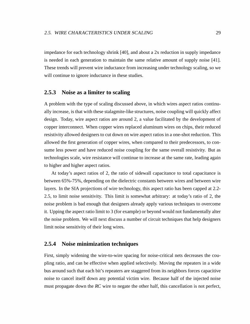
2.5. WIRE CHARACTERISTICS UNDER SCALING 29
impedance for each technology shrink [40], and about a 2x reduction in supply impedance
is needed in each generation to maintain the same relative amount of supply noise [41].
These trends will prevent wire inductance from increasing under technology scaling, so we
will continue to ignore inductance in these studies.
2.5.3 Noise as a limiter to scaling
A problem with the type of scaling discussed above, in which wires aspect ratios continu-
ally increase, is that with these stalagmite-like structures, noise coupling will quickly affect
design. Today, wire aspect ratios are around 2, a value facilitated by the development of
copper interconnect. When copper wires replaced aluminum wires on chips, their reduced
resistivity allowed designers to cut down on wire aspect ratios in a one-shot reduction. This
allowed the first generation of copper wires, when compared to their predecessors, to con-
sume less power and have reduced noise coupling for the same overall resistivity. But as
technologies scale, wire resistance will continue to increase at the same rate, leading again
to higher and higher aspect ratios.
At today’s aspect ratios of 2, the ratio of sidewall capacitance to total capacitance is
between 65%-75%, depending on the dielectric constants between wires and between wire
layers. In the SIA projections of wire technology, this aspect ratio has been capped at 2.2-
2.5, to limit noise sensitivity. This limit is somewhat arbitrary: at today’s ratio of 2, the
noise problem is bad enough that designers already apply various techniques to overcome
it. Upping the aspect ratio limit to 3 (for example) or beyond would not fundamentally alter
the noise problem. We will next discuss a number of circuit techniques that help designers
limit noise sensitivity of their long wires.
2.5.4 Noise minimization techniques
First, simply widening the wire-to-wire spacing for noise-critical nets decreases the cou-
pling ratio, and can be effective when applied selectively. Moving the repeaters in a wide
bus around such that each bit’s repeaters are staggered from its neighbors forces capacitive
noise to cancel itself down any potential victim wire. Because half of the injected noise
must propagate down the RC wire to negate the other half, this cancellation is not perfect,
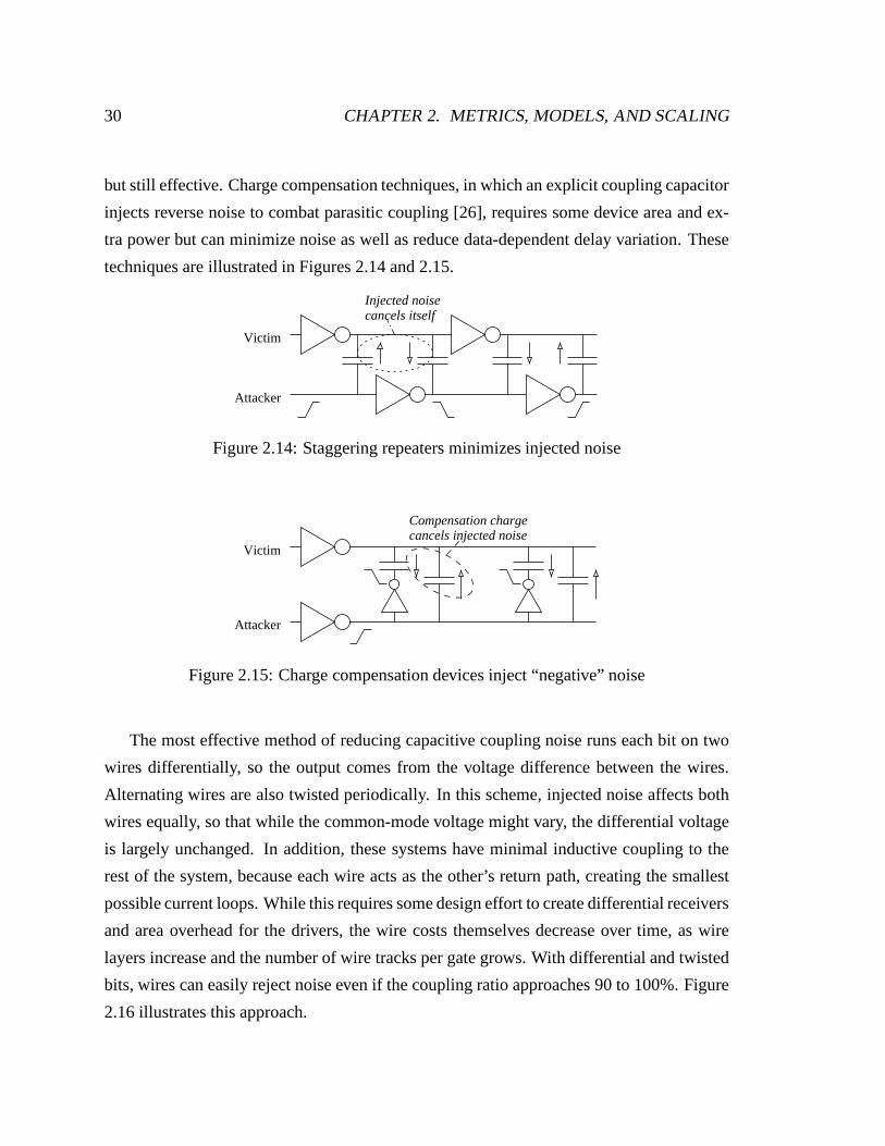
30 CHAPTER 2. METRICS, MODELS, AND SCALING
but still effective. Charge compensation techniques, in which an explicit coupling capacitor
injects reverse noise to combat parasitic coupling [26], requires some device area and ex-
tra power but can minimize noise as well as reduce data-dependent delay variation. These
techniques are illustrated in Figures 2.14 and 2.15.
Attacker
Victim
Injected noisecancels itself
Figure 2.14: Staggering repeaters minimizes injected noise
Attacker
Victimcancels injected noiseCompensation charge
Figure 2.15: Charge compensation devices inject “negative” noise
The most effective method of reducing capacitive coupling noise runs each bit on two
wires differentially, so the output comes from the voltage difference between the wires.
Alternating wires are also twisted periodically. In this scheme, injected noise affects both
wires equally, so that while the common-mode voltage might vary, the differential voltage
is largely unchanged. In addition, these systems have minimal inductive coupling to the
rest of the system, because each wire acts as the other’s return path, creating the smallest
possible current loops. While this requires some design effort to create differential receivers
and area overhead for the drivers, the wire costs themselves decrease over time, as wire
layers increase and the number of wire tracks per gate grows. With differential and twisted
bits, wires can easily reject noise even if the coupling ratio approaches 90 to 100%. Figure
2.16 illustrates this approach.
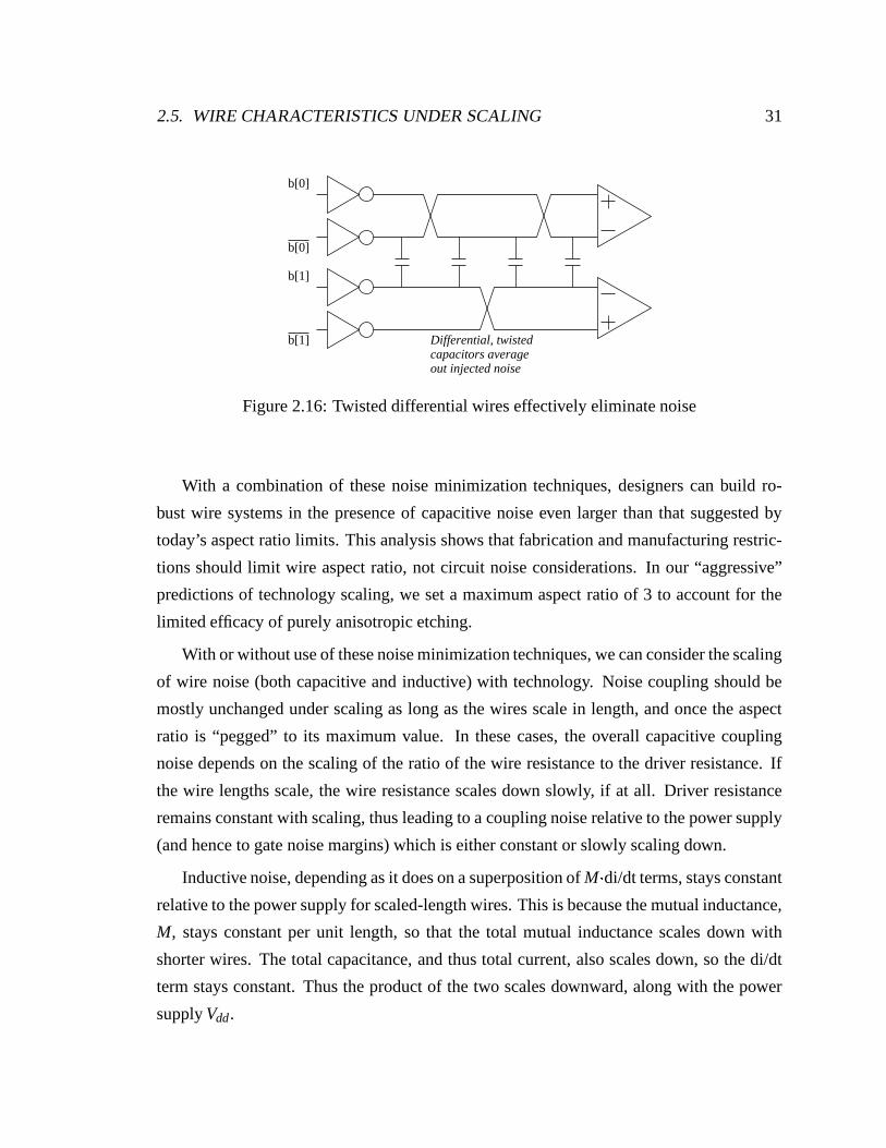
2.5. WIRE CHARACTERISTICS UNDER SCALING 31
b[0]
b[0]
b[1]
b[1]
out injected noisecapacitors averageDifferential, twisted
Figure 2.16: Twisted differential wires effectively eliminate noise
With a combination of these noise minimization techniques, designers can build ro-
bust wire systems in the presence of capacitive noise even larger than that suggested by
today’s aspect ratio limits. This analysis shows that fabrication and manufacturing restric-
tions should limit wire aspect ratio, not circuit noise considerations. In our “aggressive”
predictions of technology scaling, we set a maximum aspect ratio of 3 to account for the
limited efficacy of purely anisotropic etching.
With or without use of these noise minimization techniques, we can consider the scaling
of wire noise (both capacitive and inductive) with technology. Noise coupling should be
mostly unchanged under scaling as long as the wires scale in length, and once the aspect
ratio is “pegged” to its maximum value. In these cases, the overall capacitive coupling
noise depends on the scaling of the ratio of the wire resistance to the driver resistance. If
the wire lengths scale, the wire resistance scales down slowly, if at all. Driver resistance
remains constant with scaling, thus leading to a coupling noise relative to the power supply
(and hence to gate noise margins) which is either constant or slowly scaling down.
Inductive noise, depending as it does on a superposition of M di/dt terms, stays constant
relative to the power supply for scaled-length wires. This is because the mutual inductance,
M, stays constant per unit length, so that the total mutual inductance scales down with
shorter wires. The total capacitance, and thus total current, also scales down, so the di/dt
term stays constant. Thus the product of the two scales downward, along with the power
supply Vdd.

32 CHAPTER 2. METRICS, MODELS, AND SCALING
If the wire lengths remain constant, the increase in wire resistance will cause the capac-
itive coupling noise to increase slightly and the inductive coupling noise to grow relative to
the power supply. This increase in noise for long wires is another reason to use repeaters.
2.6 Wire performance under scaling
To properly discuss wire delays under technology scaling, we will first make a distinction
between two kinds of wires, as shown in Figure 2.17. The first kind of wire connects gates
locally within blocks. We can think of these as wires that span a block of fixed complexity;
for example, a wire that runs across a block of 1000 gates. As technology scales, these
gates get smaller, and this wire therefore gets shorter. This is the salient characteristic of
these “local wires”—they get shorter under scaling.
Chip holds four cores Chip holds nine coresScaling
Wires that don’t scale
Wires that scale
Figure 2.17: Two kinds of wire on a chip: local and global
The second kind of wire connects together sections of a die, and spans a block of
fixed physical distance. For example, we can consider a wire that spans a 5mm length
(approximately a quarter of a maximal die) regardless of technology. Under scaling, die
size does not typically decrease—we simply add more functionality to the chip, so these
“global wires” have the characteristic of remaining constant in length.
Note that this distinction between wire types does not assume specific wire lengths.
There can be short global wires that span 1/1000 of a die, for example, and there can be
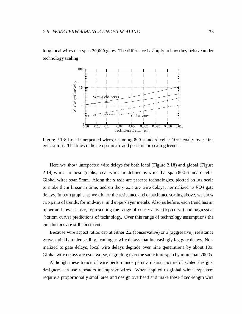
2.6. WIRE PERFORMANCE UNDER SCALING 33
long local wires that span 20,000 gates. The difference is simply in how they behave under
technology scaling.
Global wires
Semi-global wires
Technology Ldrawn (µm)
Wir
eDel
ay/G
ateD
elay
0.0130.0180.0250.0350.050.070.10.130.18
1000
100
10
1
Figure 2.18: Local unrepeated wires, spanning 800 standard cells: 10x penalty over ninegenerations. The lines indicate optimistic and pessimistic scaling trends.
Here we show unrepeated wire delays for both local (Figure 2.18) and global (Figure
2.19) wires. In these graphs, local wires are defined as wires that span 800 standard cells.
Global wires span 5mm. Along the x-axis are process technologies, plotted on log-scale
to make them linear in time, and on the y-axis are wire delays, normalized to FO4 gate
delays. In both graphs, as we did for the resistance and capacitance scaling above, we show
two pairs of trends, for mid-layer and upper-layer metals. Also as before, each trend has an
upper and lower curve, representing the range of conservative (top curve) and aggressive
(bottom curve) predictions of technology. Over this range of technology assumptions the
conclusions are still consistent.
Because wire aspect ratios cap at either 2.2 (conservative) or 3 (aggressive), resistance
grows quickly under scaling, leading to wire delays that increasingly lag gate delays. Nor-
malized to gate delays, local wire delays degrade over nine generations by about 10x.
Global wire delays are even worse, degrading over the same time span by more than 2000x.
Although these trends of wire performance paint a dismal picture of scaled designs,
designers can use repeaters to improve wires. When applied to global wires, repeaters
require a proportionally small area and design overhead and make these fixed-length wire
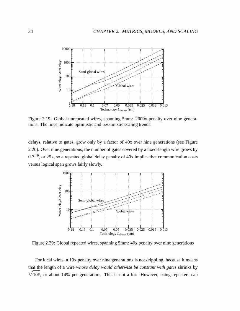
34 CHAPTER 2. METRICS, MODELS, AND SCALING
Global wires
Semi-global wires
Technology Ldrawn (µm)
Wir
eDel
ay/G
ateD
elay
0.0130.0180.0250.0350.050.070.10.130.18
10000
1000
100
10
1
Figure 2.19: Global unrepeated wires, spanning 5mm: 2000x penalty over nine genera-tions. The lines indicate optimistic and pessimistic scaling trends.
delays, relative to gates, grow only by a factor of 40x over nine generations (see Figure
2.20). Over nine generations, the number of gates covered by a fixed-length wire grows by
0 7 9, or 25x, so a repeated global delay penalty of 40x implies that communication costs
versus logical span grows fairly slowly.
Global wires
Semi-global wires
Technology Ldrawn (µm)
Wir
eDel
ay/G
ateD
elay
0.0130.0180.0250.0350.050.070.10.130.18
1000
100
10
1
Figure 2.20: Global repeated wires, spanning 5mm: 40x penalty over nine generations
For local wires, a 10x penalty over nine generations is not crippling, because it means
that the length of a wire whose delay would otherwise be constant with gates shrinks by10
19 , or about 14% per generation. This is not a lot. However, using repeaters can
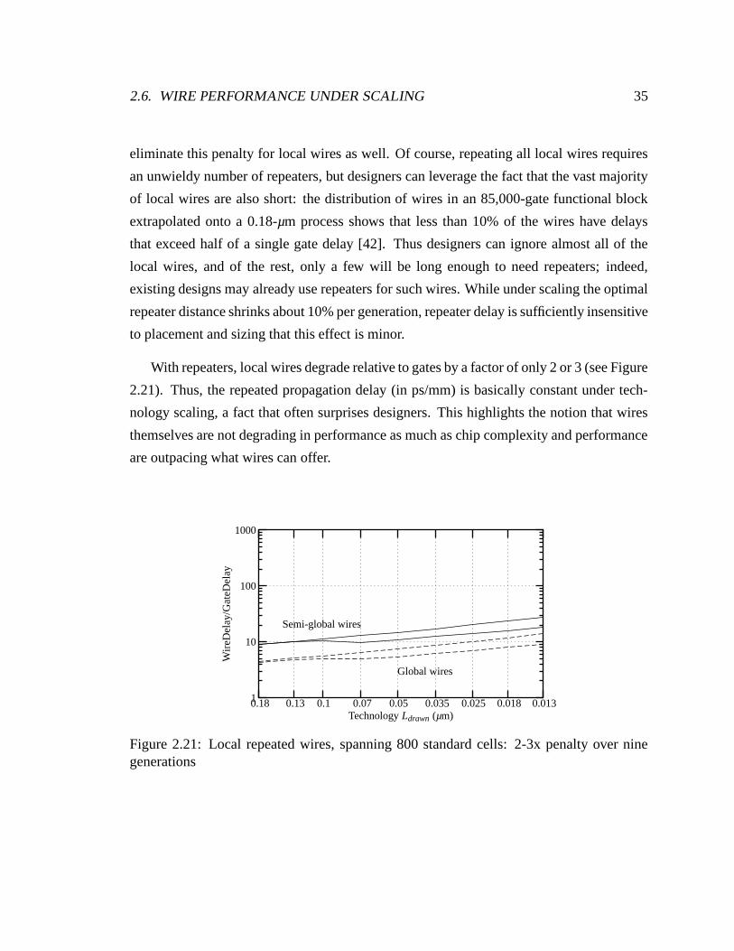
2.6. WIRE PERFORMANCE UNDER SCALING 35
eliminate this penalty for local wires as well. Of course, repeating all local wires requires
an unwieldy number of repeaters, but designers can leverage the fact that the vast majority
of local wires are also short: the distribution of wires in an 85,000-gate functional block
extrapolated onto a 0.18-µm process shows that less than 10% of the wires have delays
that exceed half of a single gate delay [42]. Thus designers can ignore almost all of the
local wires, and of the rest, only a few will be long enough to need repeaters; indeed,
existing designs may already use repeaters for such wires. While under scaling the optimal
repeater distance shrinks about 10% per generation, repeater delay is sufficiently insensitive
to placement and sizing that this effect is minor.
With repeaters, local wires degrade relative to gates by a factor of only 2 or 3 (see Figure
2.21). Thus, the repeated propagation delay (in ps/mm) is basically constant under tech-
nology scaling, a fact that often surprises designers. This highlights the notion that wires
themselves are not degrading in performance as much as chip complexity and performance
are outpacing what wires can offer.
Global wires
Semi-global wires
Technology Ldrawn (µm)
Wir
eDel
ay/G
ateD
elay
0.0130.0180.0250.0350.050.070.10.130.18
1000
100
10
1
Figure 2.21: Local repeated wires, spanning 800 standard cells: 2-3x penalty over ninegenerations
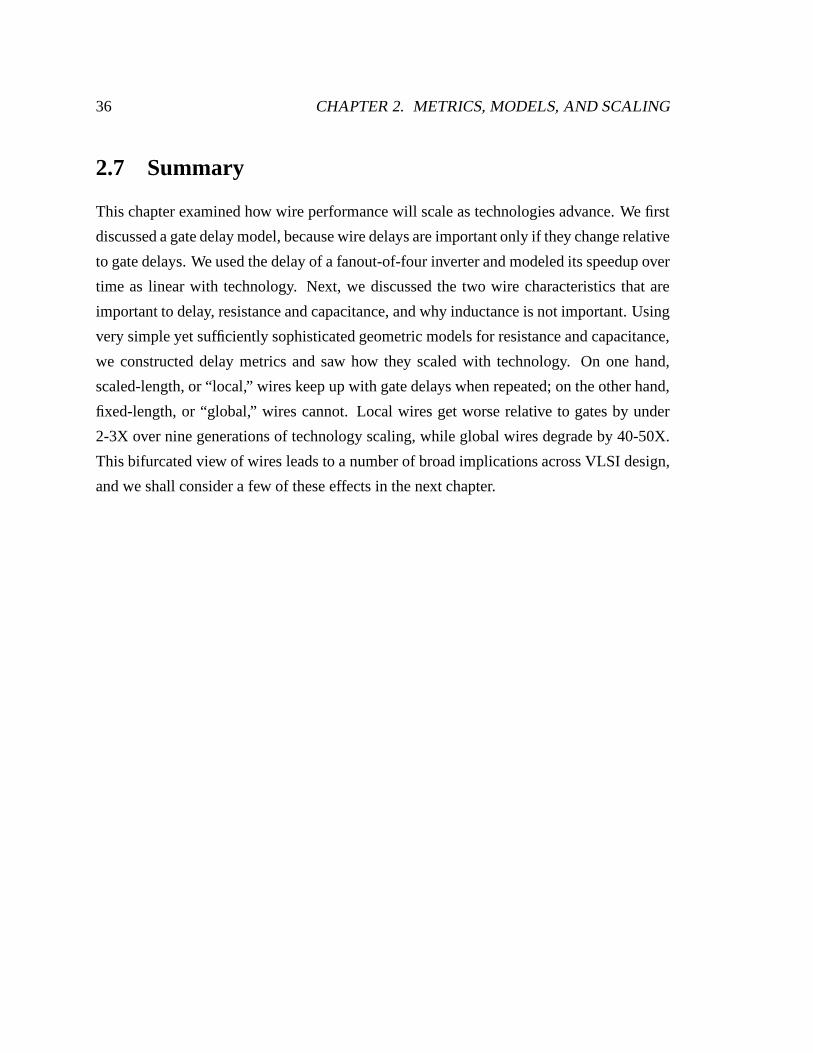
36 CHAPTER 2. METRICS, MODELS, AND SCALING
2.7 Summary
This chapter examined how wire performance will scale as technologies advance. We first
discussed a gate delay model, because wire delays are important only if they change relative
to gate delays. We used the delay of a fanout-of-four inverter and modeled its speedup over
time as linear with technology. Next, we discussed the two wire characteristics that are
important to delay, resistance and capacitance, and why inductance is not important. Using
very simple yet sufficiently sophisticated geometric models for resistance and capacitance,
we constructed delay metrics and saw how they scaled with technology. On one hand,
scaled-length, or “local,” wires keep up with gate delays when repeated; on the other hand,
fixed-length, or “global,” wires cannot. Local wires get worse relative to gates by under
2-3X over nine generations of technology scaling, while global wires degrade by 40-50X.
This bifurcated view of wires leads to a number of broad implications across VLSI design,
and we shall consider a few of these effects in the next chapter.
Chapter 3
Implications of Scaling
The previous chapter painted a future with ever-increasing gate performance, local wires
that can keep pace with these gates, and global wires that cannot. These scaling trends
have implications for all aspects of VLSI engineering. In this chapter we focus on how
scaling will affect design in two areas in particular. First, we will consider design “at the
ground level,” and examine scaling implications for gate-level designers. The vast majority
of design today happens at the gate level, with place-and-route tools automatically creating
physical instances of gates and wires. We will show that these computer-aided design
(CAD) tools will need to improve as wires scale, despite oft-cited arguments to the contrary.
Second, we will consider design “at the 50,000-foot level,” and examine scaling im-
plications for computer architecture. Modern processors follow the dominant model of
single-chip, monolithic architectures—a computing paradigm ultimately unsustainable un-
der wire scaling. We will argue for architectures that are more “wire-aware,” and advance
modular systems as one such candidate.
One interesting offshoot of these modular architectures is that global communication
becomes mediated by a very dense, regular, and structured mesh of global wires. The bad
news with these global wires is that they can potentially consume hundreds of watts of
power. The good news is that their highly ordered structure lends itself nicely to aggressive
circuit design techniques designed to save wire power. We will briefly introduce the low-
power implications of wire scaling towards the end of the chapter to motivate the efficient
circuits discussed in later chapters.
37

38 CHAPTER 3. IMPLICATIONS OF SCALING
3.1 Design at the ground level: CAD tools
VLSI designers build chips today using one of two principal methodologies that differ in
their extent of manual intervention. On one hand, microprocessors are designed by large
design teams who hand-craft custom circuits for optimal performance and manually draw
layout for high density. These designs that result have an extravagent productivity cost
but demonstrate good performance; although they take more than three years to develop,
leading-edge CPUs can run at close to 15 FO4 delays per cycle, or 2.5 to 3.0GHz in a
highly-optimized 0.13-µm process.
On the other hand, application-specific integrated chips (ASICs) that target smaller
markets are built by small design teams, who rely heavily on computer-aided design (CAD)
tools to do much of the physical work for them. These highly automated CAD flows,
used for designs such as graphics or network processors, generate structured netlists, place
layouts from standard cell libraries, and route them together. The resulting designs can be
completed very quickly—the Nvidia GeForce 4 graphics processor, with over 60 million
transistors, went from initial concept to tapeout in just nine months—but do not clock as
fast as the underlying technology permits; that same GeForce design runs at only about 40
FO4s per cycle [47].
A third design methodology, using gate arrays to compile chips, was historically im-
portant but is rapidly disappearing. While ASIC starts are predicted to be around 41,000
by 2005, gate-array starts are predicted to number only about 600 in the same year [48].
The ASIC design methodology, dominant outside of the few large CPU houses, is only
as successful as its place-and-route CAD tools. Notably, interconnect scaling may force
fundamental changes in how these tools are used: as wire delay grows, timing convergence
will become difficult or impossible to attain with current fanout-based wire load models.
In this section we explore the effects of wire scaling on CAD tools.
3.1.1 Claim: CAD tools need not improve
In a now-famous 1998 tutorial at ICCAD, Sylvester and Keutzer analyzed interconnect
scaling and its potential effects on CAD tools [49]. By examining the scaling of average-
length wires, they concluded that delays for these wires will slowly decrease relative to
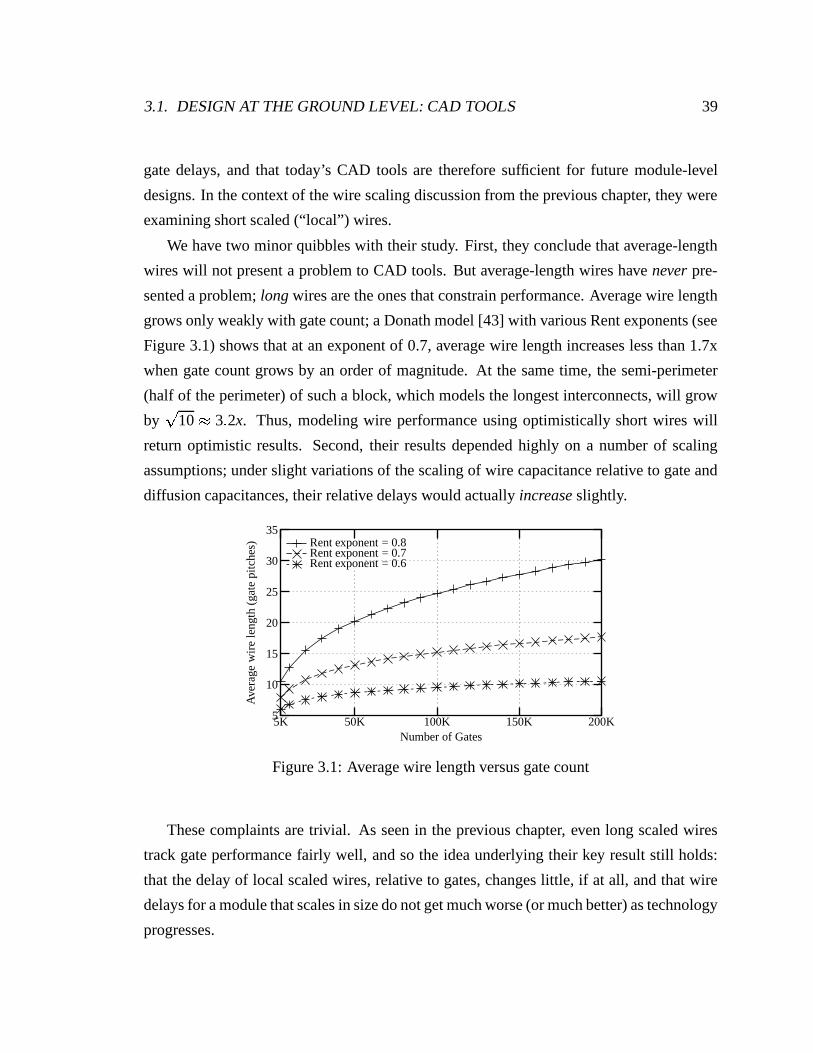
3.1. DESIGN AT THE GROUND LEVEL: CAD TOOLS 39
gate delays, and that today’s CAD tools are therefore sufficient for future module-level
designs. In the context of the wire scaling discussion from the previous chapter, they were
examining short scaled (“local”) wires.
We have two minor quibbles with their study. First, they conclude that average-length
wires will not present a problem to CAD tools. But average-length wires have never pre-
sented a problem; long wires are the ones that constrain performance. Average wire length
grows only weakly with gate count; a Donath model [43] with various Rent exponents (see
Figure 3.1) shows that at an exponent of 0.7, average wire length increases less than 1.7x
when gate count grows by an order of magnitude. At the same time, the semi-perimeter
(half of the perimeter) of such a block, which models the longest interconnects, will grow
by 10 3 2x. Thus, modeling wire performance using optimistically short wires will
return optimistic results. Second, their results depended highly on a number of scaling
assumptions; under slight variations of the scaling of wire capacitance relative to gate and
diffusion capacitances, their relative delays would actually increase slightly.
Rent exponent = 0.6Rent exponent = 0.7Rent exponent = 0.8
Number of Gates
Ave
rage
wir
ele
ngth
(gat
epi
tche
s)
200K150K100K50K5K
35
30
25
20
15
10
5
Figure 3.1: Average wire length versus gate count
These complaints are trivial. As seen in the previous chapter, even long scaled wires
track gate performance fairly well, and so the idea underlying their key result still holds:
that the delay of local scaled wires, relative to gates, changes little, if at all, and that wire
delays for a module that scales in size do not get much worse (or much better) as technology
progresses.
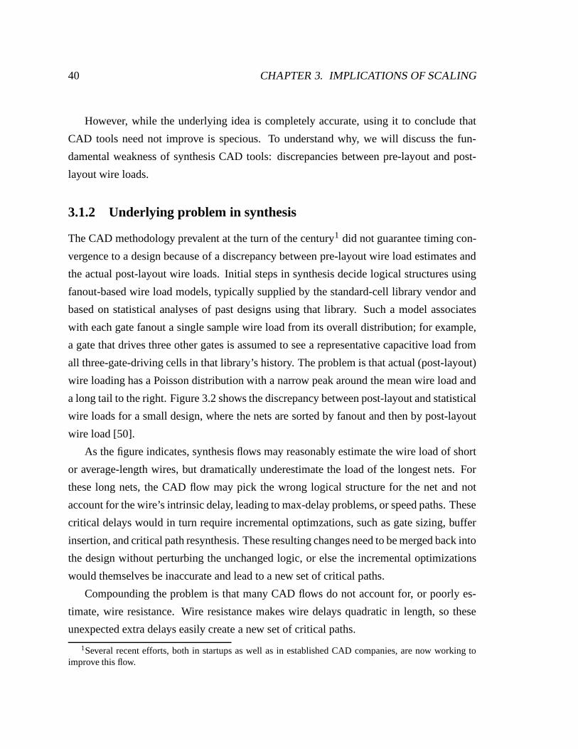
40 CHAPTER 3. IMPLICATIONS OF SCALING
However, while the underlying idea is completely accurate, using it to conclude that
CAD tools need not improve is specious. To understand why, we will discuss the fun-
damental weakness of synthesis CAD tools: discrepancies between pre-layout and post-
layout wire loads.
3.1.2 Underlying problem in synthesis
The CAD methodology prevalent at the turn of the century1 did not guarantee timing con-
vergence to a design because of a discrepancy between pre-layout wire load estimates and
the actual post-layout wire loads. Initial steps in synthesis decide logical structures using
fanout-based wire load models, typically supplied by the standard-cell library vendor and
based on statistical analyses of past designs using that library. Such a model associates
with each gate fanout a single sample wire load from its overall distribution; for example,
a gate that drives three other gates is assumed to see a representative capacitive load from
all three-gate-driving cells in that library’s history. The problem is that actual (post-layout)
wire loading has a Poisson distribution with a narrow peak around the mean wire load and
a long tail to the right. Figure 3.2 shows the discrepancy between post-layout and statistical
wire loads for a small design, where the nets are sorted by fanout and then by post-layout
wire load [50].
As the figure indicates, synthesis flows may reasonably estimate the wire load of short
or average-length wires, but dramatically underestimate the load of the longest nets. For
these long nets, the CAD flow may pick the wrong logical structure for the net and not
account for the wire’s intrinsic delay, leading to max-delay problems, or speed paths. These
critical delays would in turn require incremental optimzations, such as gate sizing, buffer
insertion, and critical path resynthesis. These resulting changes need to be merged back into
the design without perturbing the unchanged logic, or else the incremental optimizations
would themselves be inaccurate and lead to a new set of critical paths.
Compounding the problem is that many CAD flows do not account for, or poorly es-
timate, wire resistance. Wire resistance makes wire delays quadratic in length, so these
unexpected extra delays easily create a new set of critical paths.
1Several recent efforts, both in startups as well as in established CAD companies, are now working toimprove this flow.
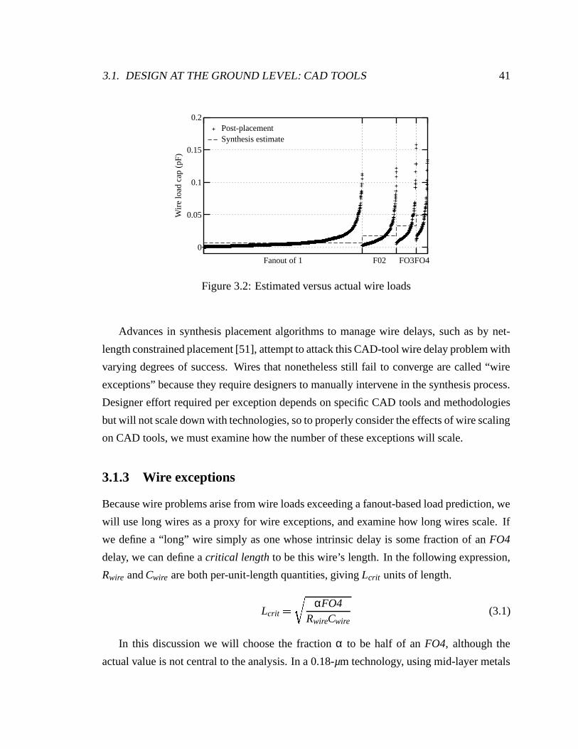
3.1. DESIGN AT THE GROUND LEVEL: CAD TOOLS 41
Synthesis estimatePost-placement
FO4FO3F02Fanout of 1
Wir
elo
adca
p(p
F)
0.2
0.15
0.1
0.05
0
Figure 3.2: Estimated versus actual wire loads
Advances in synthesis placement algorithms to manage wire delays, such as by net-
length constrained placement [51], attempt to attack this CAD-tool wire delay problem with
varying degrees of success. Wires that nonetheless still fail to converge are called “wire
exceptions” because they require designers to manually intervene in the synthesis process.
Designer effort required per exception depends on specific CAD tools and methodologies
but will not scale down with technologies, so to properly consider the effects of wire scaling
on CAD tools, we must examine how the number of these exceptions will scale.
3.1.3 Wire exceptions
Because wire problems arise from wire loads exceeding a fanout-based load prediction, we
will use long wires as a proxy for wire exceptions, and examine how long wires scale. If
we define a “long” wire simply as one whose intrinsic delay is some fraction of an FO4
delay, we can define a critical length to be this wire’s length. In the following expression,
Rwire and Cwire are both per-unit-length quantities, giving Lcrit units of length.
Lcrit
αFO4
RwireCwire(3.1)
In this discussion we will choose the fraction α to be half of an FO4, although the
actual value is not central to the analysis. In a 0.18-µm technology, using mid-layer metals
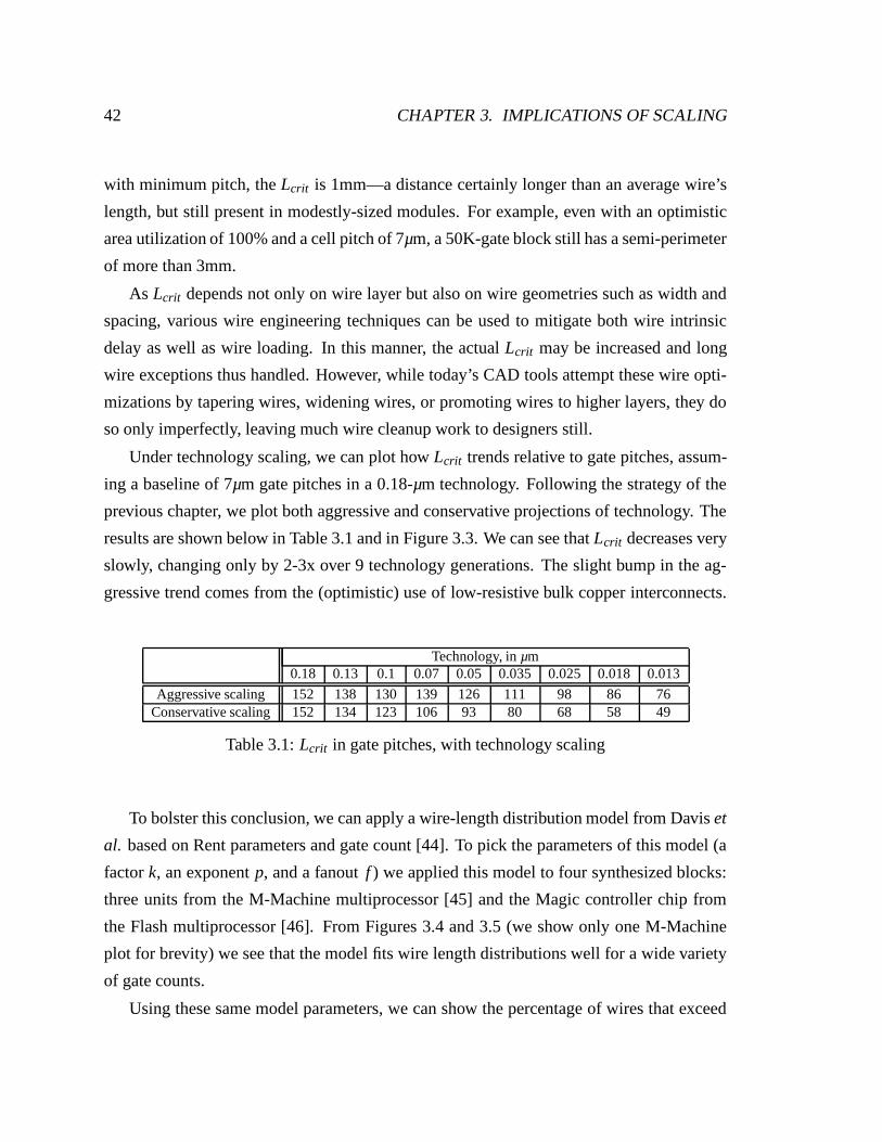
42 CHAPTER 3. IMPLICATIONS OF SCALING
with minimum pitch, the Lcrit is 1mm—a distance certainly longer than an average wire’s
length, but still present in modestly-sized modules. For example, even with an optimistic
area utilization of 100% and a cell pitch of 7µm, a 50K-gate block still has a semi-perimeter
of more than 3mm.
As Lcrit depends not only on wire layer but also on wire geometries such as width and
spacing, various wire engineering techniques can be used to mitigate both wire intrinsic
delay as well as wire loading. In this manner, the actual Lcrit may be increased and long
wire exceptions thus handled. However, while today’s CAD tools attempt these wire opti-
mizations by tapering wires, widening wires, or promoting wires to higher layers, they do
so only imperfectly, leaving much wire cleanup work to designers still.
Under technology scaling, we can plot how Lcrit trends relative to gate pitches, assum-
ing a baseline of 7µm gate pitches in a 0.18-µm technology. Following the strategy of the
previous chapter, we plot both aggressive and conservative projections of technology. The
results are shown below in Table 3.1 and in Figure 3.3. We can see that Lcrit decreases very
slowly, changing only by 2-3x over 9 technology generations. The slight bump in the ag-
gressive trend comes from the (optimistic) use of low-resistive bulk copper interconnects.
Technology, in µm0.18 0.13 0.1 0.07 0.05 0.035 0.025 0.018 0.013
Aggressive scaling 152 138 130 139 126 111 98 86 76Conservative scaling 152 134 123 106 93 80 68 58 49
Table 3.1: Lcrit in gate pitches, with technology scaling
To bolster this conclusion, we can apply a wire-length distribution model from Davis et
al. based on Rent parameters and gate count [44]. To pick the parameters of this model (a
factor k, an exponent p, and a fanout f ) we applied this model to four synthesized blocks:
three units from the M-Machine multiprocessor [45] and the Magic controller chip from
the Flash multiprocessor [46]. From Figures 3.4 and 3.5 (we show only one M-Machine
plot for brevity) we see that the model fits wire length distributions well for a wide variety
of gate counts.
Using these same model parameters, we can show the percentage of wires that exceed
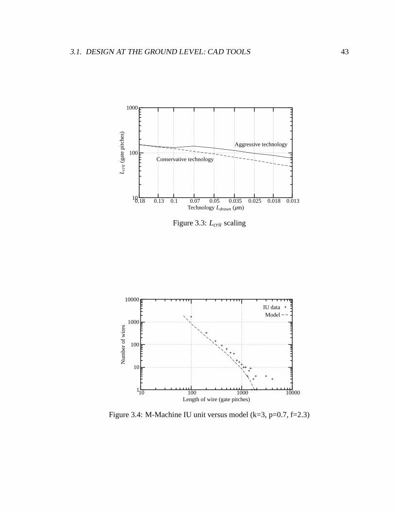
3.1. DESIGN AT THE GROUND LEVEL: CAD TOOLS 43
Conservative technology
Aggressive technology
Technology Ldrawn (µm)
Lcr
it(g
ate
pitc
hes)
0.0130.0180.0250.0350.050.070.10.130.18
1000
100
10
Figure 3.3: Lcrit scaling
ModelIU data
Length of wire (gate pitches)
Num
ber
ofw
ires
10000100010010
10000
1000
100
10
1
Figure 3.4: M-Machine IU unit versus model (k=3, p=0.7, f=2.3)
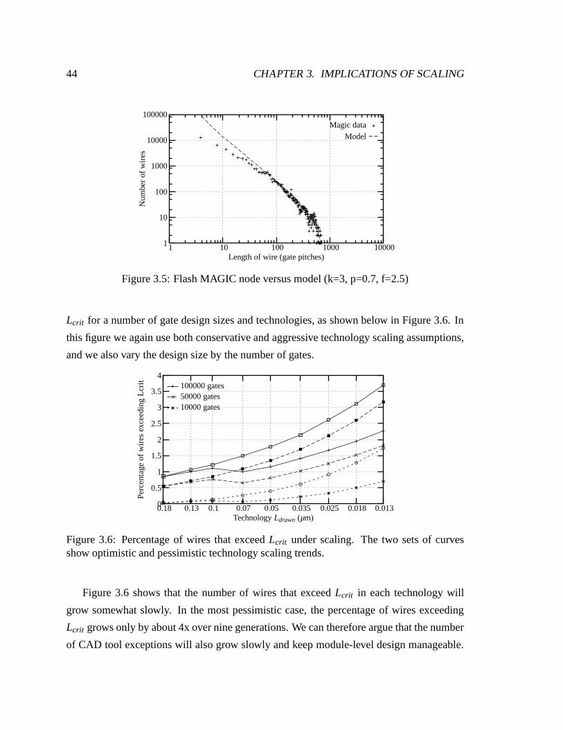
44 CHAPTER 3. IMPLICATIONS OF SCALING
ModelMagic data
Length of wire (gate pitches)
Num
ber
ofw
ires
100001000100101
100000
10000
1000
100
10
1
Figure 3.5: Flash MAGIC node versus model (k=3, p=0.7, f=2.5)
Lcrit for a number of gate design sizes and technologies, as shown below in Figure 3.6. In
this figure we again use both conservative and aggressive technology scaling assumptions,
and we also vary the design size by the number of gates.
10000 gates50000 gates100000 gates
Technology Ldrawn (µm)
Per
cent
age
ofw
ires
exce
edin
gL
crit
0.0130.0180.0250.0350.050.070.10.130.18
4
3.5
3
2.5
2
1.5
1
0.5
0
Figure 3.6: Percentage of wires that exceed Lcrit under scaling. The two sets of curvesshow optimistic and pessimistic technology scaling trends.
Figure 3.6 shows that the number of wires that exceed Lcrit in each technology will
grow somewhat slowly. In the most pessimistic case, the percentage of wires exceeding
Lcrit grows only by about 4x over nine generations. We can therefore argue that the number
of CAD tool exceptions will also grow slowly and keep module-level design manageable.
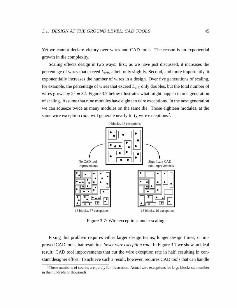
3.1. DESIGN AT THE GROUND LEVEL: CAD TOOLS 45
Yet we cannot declare victory over wires and CAD tools. The reason is an exponential
growth in die complexity.
Scaling effects design in two ways: first, as we have just discussed, it increases the
percentage of wires that exceed Lcrit, albeit only slightly. Second, and more importantly, it
exponentially increases the number of wires in a design. Over five generations of scaling,
for example, the percentage of wires that exceed Lcrit only doubles, but the total number of
wires grows by 25 32. Figure 3.7 below illustrates what might happen in one generation
of scaling. Assume that nine modules have eighteen wire exceptions. In the next generation
we can squeeze twice as many modules on the same die. Those eighteen modules, at the
same wire exception rate, will generate nearly forty wire exceptions2.
No CAD toolimprovements
Significant CADtool improvements
18 blocks, 19 exceptions
9 blocks, 18 exceptions
18 blocks, 37 exceptions
Figure 3.7: Wire exceptions under scaling
Fixing this problem requires either larger design teams, longer design times, or im-
proved CAD tools that result in a lower wire exception rate. In Figure 3.7 we show an ideal
result: CAD tool improvements that cut the wire exception rate in half, resulting in con-
stant designer effort. To achieve such a result, however, requires CAD tools that can handle
2These numbers, of course, are purely for illustration. Actual wire exceptions for large blocks can numberin the hundreds or thousands.
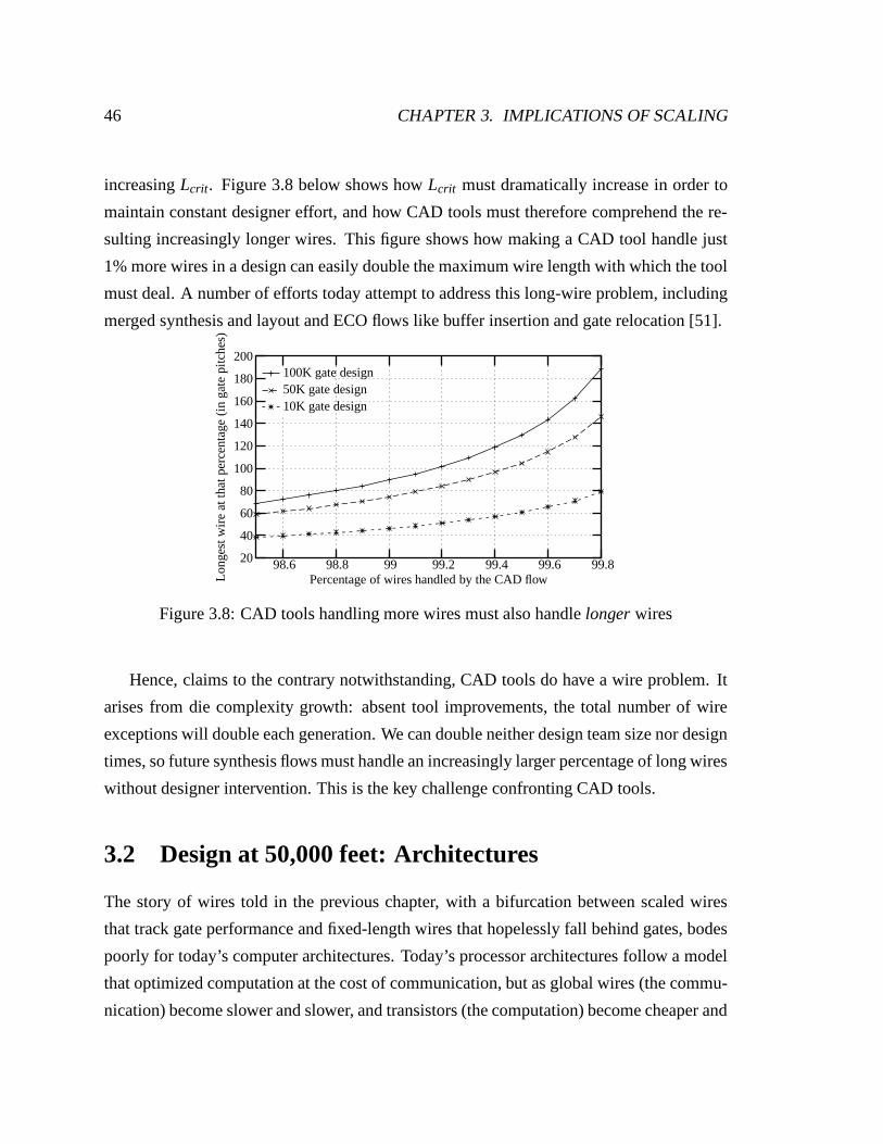
46 CHAPTER 3. IMPLICATIONS OF SCALING
increasing Lcrit. Figure 3.8 below shows how Lcrit must dramatically increase in order to
maintain constant designer effort, and how CAD tools must therefore comprehend the re-
sulting increasingly longer wires. This figure shows how making a CAD tool handle just
1% more wires in a design can easily double the maximum wire length with which the tool
must deal. A number of efforts today attempt to address this long-wire problem, including
merged synthesis and layout and ECO flows like buffer insertion and gate relocation [51].
10K gate design50K gate design100K gate design
Percentage of wires handled by the CAD flowLon
gest
wir
eat
that
perc
enta
ge(i
nga
tepi
tche
s)
99.899.699.499.29998.898.6
200
180
160
140
120
100
80
60
40
20
Figure 3.8: CAD tools handling more wires must also handle longer wires
Hence, claims to the contrary notwithstanding, CAD tools do have a wire problem. It
arises from die complexity growth: absent tool improvements, the total number of wire
exceptions will double each generation. We can double neither design team size nor design
times, so future synthesis flows must handle an increasingly larger percentage of long wires
without designer intervention. This is the key challenge confronting CAD tools.
3.2 Design at 50,000 feet: Architectures
The story of wires told in the previous chapter, with a bifurcation between scaled wires
that track gate performance and fixed-length wires that hopelessly fall behind gates, bodes
poorly for today’s computer architectures. Today’s processor architectures follow a model
that optimized computation at the cost of communication, but as global wires (the commu-
nication) become slower and slower, and transistors (the computation) become cheaper and
3.2. DESIGN AT 50,000 FEET: ARCHITECTURES 47
cheaper, this architectural model will become ultimately unsustainable.
3.2.1 A historical perspective
Modern processor architectures evolved when transistors were precious and on-chip com-
munication was cheap. As a result, a theme of functional centralization and reuse pre-
vailed, with an emphasis on monolithic global resources made available to multiple con-
sumers [54][55]. For a long time, wire access to such resources was low-latency, making
this model attractive to architects and programmers: it presented the most uniform com-
putational framework for the best utilization of functional units. This focus on function
rather than communication pervades all aspects of design. Consider hardware description
languages like Verilog, for instance: in Verilog code, each line represents a function, and
communication between different functions, or lines of code, are implied only by variable
names.
In older technology generations, few functional units actually fit on a die, so maximal
use of these few functional units was paramount, and fitting all the needed functions on
the chip was the critical design goal. The number of gates that fit on a 2.0-µm technology
chip was less than 50K, the size of today’s synthesized blocks. Cross-chip wires were not
a problem, because their logical span was so short, and wire resistance was not an issue.
As technologies improved, wire resistance remained small, but the increasing capac-
itance of long wires became significant. Floorplanning of high-performance designs be-
came an important design step, so that proper device sizing could keep communication
costs low. Continued technology scaling led to the situation where global wire delays were
non-trivial but still much less than a clock cycle. In this design period, the programming
model remained one of globally shared resources, but with micro-architectures increasingly
partitioned. For example, the instruction fetch unit, while logically part of the datapath,
physically migrated to the cache to minimize branch latencies. The address adder in many
machines was duplicated: one in the datapath where it logically belonged, and a smaller
version near the data cache to generate the cache index, again to reduce latency. Wires de-
lays were still modest (much less than a cycle), and these micro-architecture changes were
mostly invisible to the user.
48 CHAPTER 3. IMPLICATIONS OF SCALING
Designers developed many tools and methodologies to handle the increasing impor-
tance of wires during this period (the beginning of sub-micron design), including analyti-
cal wire RC models and more accurate wire simulation tools such as asymptotic waveform
evaluation [56]; floorplanning techniques such as delay-driven segregation of local and
global routing; and local circuit generation techniques such as layout-driven synthesis. A
modern 0.18-µm design utilizes some or all of the above techniques. While local rout-
ing within reasonably-sized blocks has negligible wire delays, global routes between such
blocks are closer to half a cycle. The cost of communication is becoming more explicit.
Chips are partitioned early in the design process, and the delays of global lines are rolled
into timing models.
As the complexity of digital systems has continued to increase, architects have re-
sponded to higher communication costs by further partitioning internal micro-architectures
and adding internal latency (pipe stages) in locations that will least damage machine per-
formance. While some researchers imply that the delay of global wires sets cycle times
[57][58], in high-performance machines this is not true; communication on these global
wires is simply pipelined. This additional internal latency allows the machines to absorb
the penalty of on-chip wires while still taking advantage of their high bandwidth. These
added latencies are now visible to the user, but have small effects on the programming
model. For example, in the Alpha 21264 processor, the integer unit is partitioned into two
clusters, and the latency for communicating between these clusters takes an additional cy-
cle [59]; and in the latest Itanium-class processor, a pair of pipeline stages were added to
account for wire delays to get to and from the 6MB level-three cache [52].
These micro-architectural techniques can hide minor global wire delays, but not if these
delays continue to expand as described in Chapter 2. Wires delays to, from, and over
monolithic architectural units that grow to multiple clock cycles will degrade system per-
formance. As a result, increasing system parallelism and complexity with global models
will be increasingly difficult: if we try to exploit technology scaling by increasing the size
of centralized resources, we will pay the damaging performance costs of long wires.
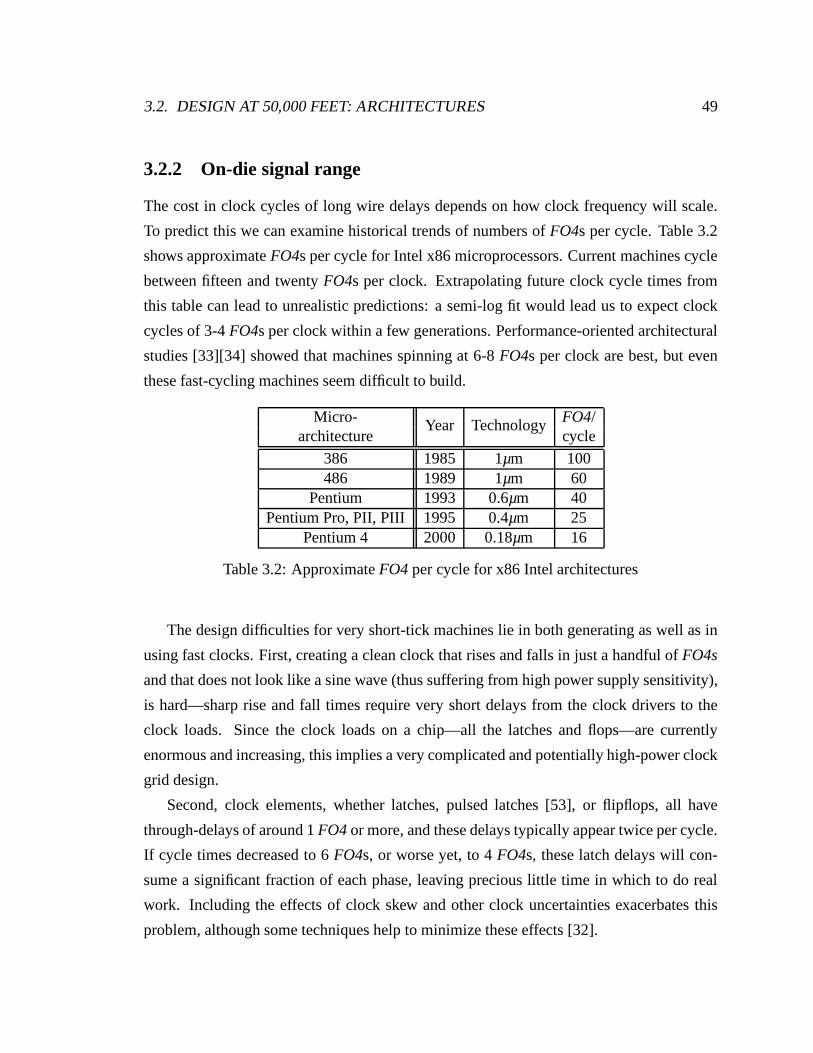
3.2. DESIGN AT 50,000 FEET: ARCHITECTURES 49
3.2.2 On-die signal range
The cost in clock cycles of long wire delays depends on how clock frequency will scale.
To predict this we can examine historical trends of numbers of FO4s per cycle. Table 3.2
shows approximate FO4s per cycle for Intel x86 microprocessors. Current machines cycle
between fifteen and twenty FO4s per clock. Extrapolating future clock cycle times from
this table can lead to unrealistic predictions: a semi-log fit would lead us to expect clock
cycles of 3-4 FO4s per clock within a few generations. Performance-oriented architectural
studies [33][34] showed that machines spinning at 6-8 FO4s per clock are best, but even
these fast-cycling machines seem difficult to build.
Micro- FO4/architecture
Year Technologycycle
386 1985 1µm 100486 1989 1µm 60
Pentium 1993 0.6µm 40Pentium Pro, PII, PIII 1995 0.4µm 25
Pentium 4 2000 0.18µm 16
Table 3.2: Approximate FO4 per cycle for x86 Intel architectures
The design difficulties for very short-tick machines lie in both generating as well as in
using fast clocks. First, creating a clean clock that rises and falls in just a handful of FO4s
and that does not look like a sine wave (thus suffering from high power supply sensitivity),
is hard—sharp rise and fall times require very short delays from the clock drivers to the
clock loads. Since the clock loads on a chip—all the latches and flops—are currently
enormous and increasing, this implies a very complicated and potentially high-power clock
grid design.
Second, clock elements, whether latches, pulsed latches [53], or flipflops, all have
through-delays of around 1 FO4 or more, and these delays typically appear twice per cycle.
If cycle times decreased to 6 FO4s, or worse yet, to 4 FO4s, these latch delays will con-
sume a significant fraction of each phase, leaving precious little time in which to do real
work. Including the effects of clock skew and other clock uncertainties exacerbates this
problem, although some techniques help to minimize these effects [32].
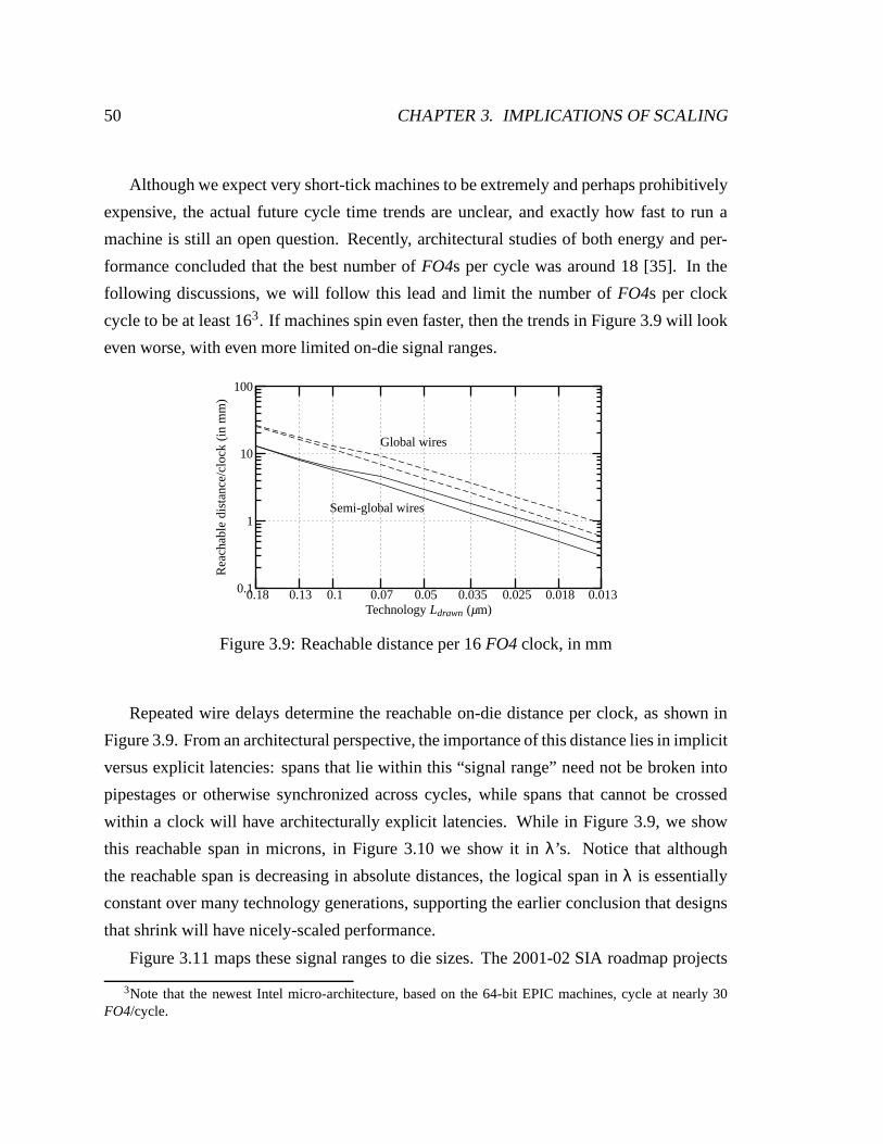
50 CHAPTER 3. IMPLICATIONS OF SCALING
Although we expect very short-tick machines to be extremely and perhaps prohibitively
expensive, the actual future cycle time trends are unclear, and exactly how fast to run a
machine is still an open question. Recently, architectural studies of both energy and per-
formance concluded that the best number of FO4s per cycle was around 18 [35]. In the
following discussions, we will follow this lead and limit the number of FO4s per clock
cycle to be at least 163. If machines spin even faster, then the trends in Figure 3.9 will look
even worse, with even more limited on-die signal ranges.
Semi-global wires
Global wires
Technology Ldrawn (µm)
Rea
chab
ledi
stan
ce/c
lock
(in
mm
)
0.0130.0180.0250.0350.050.070.10.130.18
100
10
1
0.1
Figure 3.9: Reachable distance per 16 FO4 clock, in mm
Repeated wire delays determine the reachable on-die distance per clock, as shown in
Figure 3.9. From an architectural perspective, the importance of this distance lies in implicit
versus explicit latencies: spans that lie within this “signal range” need not be broken into
pipestages or otherwise synchronized across cycles, while spans that cannot be crossed
within a clock will have architecturally explicit latencies. While in Figure 3.9, we show
this reachable span in microns, in Figure 3.10 we show it in λ’s. Notice that although
the reachable span is decreasing in absolute distances, the logical span in λ is essentially
constant over many technology generations, supporting the earlier conclusion that designs
that shrink will have nicely-scaled performance.
Figure 3.11 maps these signal ranges to die sizes. The 2001-02 SIA roadmap projects
3Note that the newest Intel micro-architecture, based on the 64-bit EPIC machines, cycle at nearly 30FO4/cycle.
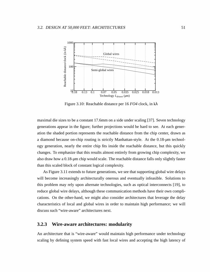
3.2. DESIGN AT 50,000 FEET: ARCHITECTURES 51
Semi-global wires
Global wires
Technology Ldrawn (µm)
Rea
chab
ledi
stan
ce/c
lock
(in
kλ)
0.0130.0180.0250.0350.050.070.10.130.18
1000
100
10
Figure 3.10: Reachable distance per 16 FO4 clock, in kλ
maximal die sizes to be a constant 17.6mm on a side under scaling [37]. Seven technology
generations appear in the figure; further projections would be hard to see. At each gener-
ation the shaded portion represents the reachable distance from the chip center, drawn as
a diamond because on-chip routing is strictly Manhattan-style. At the 0.18-µm technol-
ogy generation, nearly the entire chip fits inside the reachable distance, but this quickly
changes. To emphasize that this results almost entirely from growing chip complexity, we
also draw how a 0.18-µm chip would scale. The reachable distance falls only slightly faster
than this scaled block of constant logical complexity.
As Figure 3.11 extends to future generations, we see that supporting global wire delays
will become increasingly architecturally onerous and eventually infeasible. Solutions to
this problem may rely upon alternate technologies, such as optical interconnects [19], to
reduce global wire delays, although these communication methods have their own compli-
cations. On the other-hand, we might also consider architectures that leverage the delay
characteristics of local and global wires in order to maintain high performance; we will
discuss such “wire-aware” architectures next.
3.2.3 Wire-aware architectures: modularity
An architecture that is “wire-aware” would maintain high performance under technology
scaling by defining system speed with fast local wires and accepting the high latency of
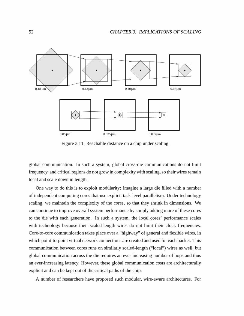
52 CHAPTER 3. IMPLICATIONS OF SCALING
mµ0.07mµ0.10mµ0.13mµ0.18
mµ0.05 mµ0.025 mµ0.035
Figure 3.11: Reachable distance on a chip under scaling
global communication. In such a system, global cross-die communications do not limit
frequency, and critical regions do not grow in complexity with scaling, so their wires remain
local and scale down in length.
One way to do this is to exploit modularity: imagine a large die filled with a number
of independent computing cores that use explicit task-level parallelism. Under technology
scaling, we maintain the complexity of the cores, so that they shrink in dimensions. We
can continue to improve overall system performance by simply adding more of these cores
to the die with each generation. In such a system, the local cores’ performance scales
with technology because their scaled-length wires do not limit their clock frequencies.
Core-to-core communication takes place over a “highway” of general and flexible wires, in
which point-to-point virtual network connections are created and used for each packet. This
communication between cores runs on similarly scaled-length (“local”) wires as well, but
global communication across the die requires an ever-increasing number of hops and thus
an ever-increasing latency. However, these global communication costs are architecturally
explicit and can be kept out of the critical paths of the chip.
A number of researchers have proposed such modular, wire-aware architectures. For
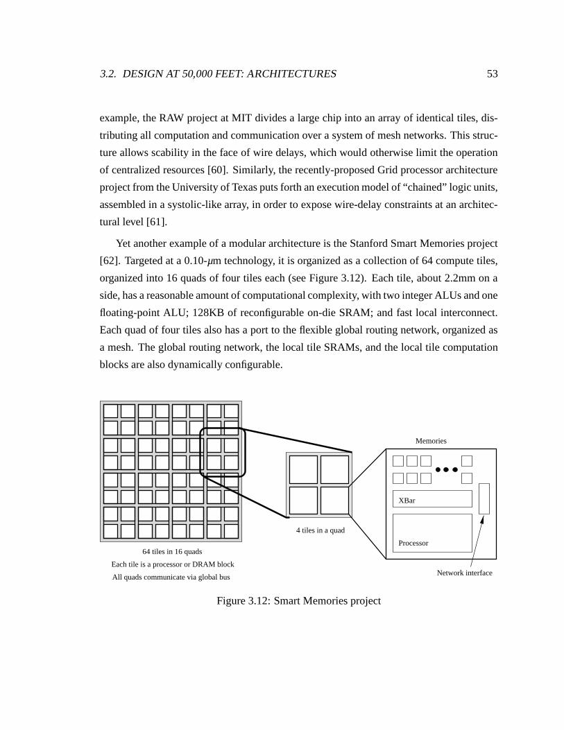
3.2. DESIGN AT 50,000 FEET: ARCHITECTURES 53
example, the RAW project at MIT divides a large chip into an array of identical tiles, dis-
tributing all computation and communication over a system of mesh networks. This struc-
ture allows scability in the face of wire delays, which would otherwise limit the operation
of centralized resources [60]. Similarly, the recently-proposed Grid processor architecture
project from the University of Texas puts forth an execution model of “chained” logic units,
assembled in a systolic-like array, in order to expose wire-delay constraints at an architec-
tural level [61].
Yet another example of a modular architecture is the Stanford Smart Memories project
[62]. Targeted at a 0.10-µm technology, it is organized as a collection of 64 compute tiles,
organized into 16 quads of four tiles each (see Figure 3.12). Each tile, about 2.2mm on a
side, has a reasonable amount of computational complexity, with two integer ALUs and one
floating-point ALU; 128KB of reconfigurable on-die SRAM; and fast local interconnect.
Each quad of four tiles also has a port to the flexible global routing network, organized as
a mesh. The global routing network, the local tile SRAMs, and the local tile computation
blocks are also dynamically configurable.
64 tiles in 16 quads
Each tile is a processor or DRAM block
All quads communicate via global bus
4 tiles in a quad
Processor
XBar
Memories
Network interface
Figure 3.12: Smart Memories project
54 CHAPTER 3. IMPLICATIONS OF SCALING
Benefits of a modular architecture
Modularity in architectures leads to a number of advantages. First and foremost, dividing a
chip into local computation with global communication enforces a sense of wire-awareness.
By elevating all cross-die communication to a mesh of global wires, in which request and
reply packets get routed out and in with high latency, we make long wires architecturally
visible in the programming model. Of course, on-chip wires are also cheap, and grow-
ing cheaper as advances in technology offer more wire layers, so on-chip wires still offer
enormous bandwidth.
Second, modular architectures suggest a way to escape the spiraling costs of design and
verification teams. A recent third-generation Itanium microprocessor with nearly half a
billion transistors (25 million in the core and 385 million on the on-chip cache) consumed
almost a thousand person-years in design and verification [52]. As we look towards chips
with billions—or tens of billions—of transistors on them, unless productivity rates grow
exponentially, we can forsee that design and verification costs will make large micropro-
cessor design prohibitively expensive for all but a handful of companies. Using modularity
to design a small block once and then replicating it over a die allows us to apply a “divide-
and-conquer” tactic to design and verification.
Third, modularity invites flexibility. Utilizing all of the offered modules of an architec-
ture becomes easier if the modules can be programmed to behave in different ways. In the
case of the Smart Memories modular architecture, a great deal of flexibility arises from a
concerted effort to make the machine dynamically reconfigurable: each CPU can be config-
ured to act as a two-way superscalar machine, a VLIW machine, or an explicitly-controlled
microcoded machine. In addition, the local SRAM blocks on each tile can be reconfigured
to resemble regular random-access memories, caches, or stream buffers. Finally, the local
and global interconnects can be reconfigured on the fly to dynamically route data within
and between modules.
This reconfigurability and flexibility has an important cost benefit. Fabricating any chip
requires the patterning of the lithographic masks used to “stencil” the chip substrate, and
the cost of making these masks is growing rapidly: in two more technology generations,

3.3. EFFICIENT GLOBAL WIRING NETWORKS 55
a full mask set will cost upwards of ten million dollars [63]. This trend threatens “fine-
line” prototyping and raises doubts about the affordability of ASICs. However, flexible and
dynamically reconfigurable architectures offer the possibility of using a single chip (and
mask set) for solving a number of different problems.
Finally, modularity in architectures offers us the benefits of global wiring homogeneity.
Because global core-to-core wiring consists of a regular and reconfigurable mesh network,
these wires are highly structured and thus have very well-characterized layouts and envi-
ronments. By constrast, monolithic architectures would have largely random global wiring.
The advantages of this global wire regularity is that it offers a clean environment for circuit
families that might otherwise be considered too risky or too design-intensive for random
wiring, but that offer large performance, noise, or power gains. In the last section of this
chapter we will consider one such circuit family, low-voltage-swing signaling, and why it
might be useful.
3.3 Efficient global wiring networks
The scalable design cost of a very high-bandwidth, flexible global routing network is not
area, because as wire layers increase with technology, the number of wire pitches per gate
continues to grow. Rather, the cost of a global routing network lies in power consumption.
The Smart Memories global network consists of a number of 128-bit buses, each spanning
2.5mm in length. These buses can support a peak aggregate bandwidth of over a terabyte
per second, but in doing so would also consume nearly 80W of switching energy in the
wires and their repeaters. Rarely do networks achieve their peak performance, but even
at a more likely 25% or 30% utilization, the global network will consume from 20-25W.
Under technology scaling, with chip voltages falling slower than feature sizes, this global
network power will not scale down with technology, meaning that current delivery and
thermal control will become increasingly difficult.4
A natural idea to reduce wire power is to reduce the voltage swing on the wires: this
4Reduction of the global network power may not be the lowest-hanging fruit (the cores combine, on paper,to consume far more power than the global wires), but useful to explore nonetheless.
56 CHAPTER 3. IMPLICATIONS OF SCALING
leads to a linear power reduction directly, and if the voltage supply driving the wires is low-
ered as well, to a quadratic reduction in consumed power. However, such low-voltage sig-
naling is fraught with danger: induced noise and timing uncertainty make the performance-
robustness tradeoffs for low-swing circuits difficult to navigate. In a later chapter we will
discuss the principal issues involved with low-swing on-die wiring systems, but first we
should ask if simpler schemes might be equally effective for much lower design costs, and
in the next chapter we consider some of these simpler approaches.
3.4 Summary
In this chapter we considered some implications of wire scaling as they applied to two
opposite corners of the VLSI design space. First, at the basic level of circuit and layout
synthesis, we looked at how wire scaling will affect the use and effectiveness of CAD
tools. Despite some claims to the contrary, wire scaling will require CAD tools to improve
dramatically in their ability to route and converge on designs with long wires. This is not
because modules are getting more and more complicated, but rather because dies are gath-
ering more and more modules. Second, at the more global level of system architecture, we
considered how an awareness of the disparity between scaled and fixed-length wires could
be made explicit to the underlying machine by exploiting modularity. We briefly discussed
three proposed machines: the MIT RAW project, the UT-Austin GPA machine, and the
Stanford Smart Memories reconfigurable architecture. All are highly modular, and thus
all provide the wire-awareness, the design productivity boost, and the potential cost benefit
from the machine flexibility that arises with such modularity. Finally, we discussed how the
global network of such modular machines is highly structured and characterized, making
it a natural bed for otherwise risky circuits like low-swing interconnects. In the successive
chapters we will consider both simple and complex methods of saving interconnect energy.
Chapter 4
Efficient Repeaters
At the end of the previous chapter we discussed the energy cost in switching a global
network of flexible wires. While it is not the dominant consumer of energy in large chips,
it is still significant. This chapter will examine some design tradeoffs that arise when
we try to limit this wire energy. We will first briefly discuss coding methods to reduce
energy usage, which can be implemented separately from any circuit optimizations. The
bulk of the chapter will deal with circuit techniques: revisiting the well-known CMOS
repeater sizing problem and solution and discussing the effects of including energy in the
formulation. We will then extend this discussion to other types of repeaters. Because
the energy gain from these types of optimizations are small at best, the next chapter will
consider more the aggressive power-savings technique of low-voltage swing circuitry.
4.1 Coding for energy savings
By exploiting the property of CMOS circuits that energy is only dissipated when voltages
change, designers can encode data transitions to minimize such events. On-chip wires only
burn energy when bits flip, so in this encoding scheme, each n-bit data word is compared
with the immediately previous n-bit data word. If more than half of the n bits need to flip
from the previous word, then the inverse of the data word is transmitted instead. An extra
single-bit control wire tells the receiver whether or not to flip the received data word [66].
To estimate the energy savings in this system, we can consider the number of wires
57

58 CHAPTER 4. EFFICIENT REPEATERS
that flip between data words. Assuming a perfectly random data distribution, an n-bit bus
carrying a particular data word will have 2n possible next data words with equal probability.
One of those next-word possibilities will have no bit changes (i.e. the same word, repeated),
and one will have all bit changes. For the rest, the number of next-word possibilities that
have k bit changes equals the number of combinations of n items chosen k ways. On
average, the total number of flipped bits is simply half the bus width:
Average bits flipped 12n
n
∑i 0
ni i
n2
(4.1)
If we now selectively invert the data word, some of these terms will have a lower “cost.”
For example, the next-word possibility that would normally flip all the bits will now flip
none of the data bits, and just the control wire. We can express this as
Avg. bits flipped, inverted 12n n
2 ∑i 0
ni i
n
∑i n
2 1
ni
n i 12
(4.2)
where the last term of 12 represents the control wire flipping half of the time. We expect
that the benefits to very small buses to be small, because the overhead of the extra control
wire will be important. On the other hand, the benefits to wide buses should also be small,
as the probability of hitting a “good” combination of words will be remote: most of the
next word possibilities will be clustered towards n2 bits flipping, where bus-invert helps,
but only minimally. The energy savings, in terms of number of bits flipping, is shown in
Table 4.1.
These results imply that bus-invert, done on buses in groups of eight bits, can be a rea-
sonable power-savings scheme. Its costs include extra latency at the start of the transmis-
sion, for the driver to perform a bitwise XOR between the current and previous data words
and then count the “1”’s that result, as well as extra latency at the end of the transmission,
for the receiver to decide whether to invert the data word or not. For bandwidth-sensitive
but latency-insensitive applications, these costs are not onerous, because we can hide the
encoding and decoding costs in an extra clock period. The encoding and decoding logic
also consume energy, to clock the registers that pipeline the data words, to do the XOR-ing

4.1. CODING FOR ENERGY SAVINGS 59
Avg. # of Avg. # ofBus width bits flipped bits flipped Savings
w/bus-invert
2 1 1.00 0.00%4 2 1.75 12.50%8 4 3.41 14.84%
16 8 6.93 13.39%32 16 14.26 10.87%64 32 29.32 8.37%
128 64 60.00 6.26%256 128 122.12 4.59%512 256 247.48 3.33%
Table 4.1: Savings from using bus-invert
and majority-counting (see Figure 4.1) on the transmission end, and to do the inverting and
muxing on the receiver end. With sufficiently long interconnect, the wire capacitive load
will dominate the switched capacitance in the logic, maintaining the energy savings. The
majority counting amplifier can be implemented as a simple amplifier, with small sizes to
minimize power consumption; the normally deleterious effects of transistor offsets only
hurt by reducing energy savings.
f[0]a[0]
b[0]
f[1] f[8]
clk
clk clk
invert
4x4x
Figure 4.1: Bus-invert transmission logic
For dynamically signalled schemes, where wires toggle between a precharge and an
evaluation voltage, buses can be encoded to minimize the number of bits that evaluate. For

60 CHAPTER 4. EFFICIENT REPEATERS
example, codings that limit the number of “1”s can save power on a domino bus. Prior work
focused on reducing chip I/O power looked at very similar schemes [67][68][69], because
chip I/O’s use resistive pullup loads and dissipate power on pull-down values. Those same
techniques are applicable here as well.
Side-to-side wire coupling dominates interconnect capacitance, so designers might be
tempted to try encoding schemes that aim to minimize switched capacitance [70]. For ex-
ample, we might map an n-bit bus onto m wires (m n) such that wires with rising edges
are not placed next to wires with falling edges (and vice versa). A simple example would
use 2n wires to transmit n bits, weaving a power supply line between each actual bit. How-
ever, this and similar encoding schemes only reduce worst-case power (as well as worst-
case noise and worst-case delay), and leave the average power dissipation unchanged; they
also increase the minimum power dissipation. In this example, we would rather simply re-
move the interleaved power supply lines to significantly reduce both maximum and average
power for the same area cost.
We might also try mapping n wires onto m wires (again, m n) to save transitions
between successive words. A trivial example would expand an 8-bit bus into 256 wires.
On average, an 8-bit bus will have four bits transitioning between consecutive words, but
the expanded 256 bits will be “1-hot,” and so at the most have only two transitions be-
tween consecutive words. However, again by simply expanding our eight wires’ spacing
to consume more area (and not even 256 wires’ worth) we can achieve much more energy
savings.
Encoding for low-power can be seen as an optimization above, and orthogonal to, the
physical layer of the actual interconnect circuitry. Therefore, we can assume that the actual
bitstream to be transmitted down a wire has already been optimally encoded and concern
ourselves with the task of physically signaling the bits down repeated wires. As we shall
see in the next chapter, by reducing the signal swing, we can make the energy consumed
in the wires a small percentage of the total energy required to transmit a token. Because
coding schemes increase driver and receiver power in order to reduce wire power, they
become less appealing with low-swing systems.
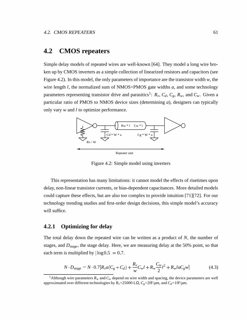
4.2. CMOS REPEATERS 61
4.2 CMOS repeaters
Simple delay models of repeated wires are well-known [64]. They model a long wire bro-
ken up by CMOS inverters as a simple collection of linearized resistors and capacitors (see
Figure 4.2). In this model, the only parameters of importance are the transistor width w, the
wire length l, the normalized sum of NMOS+PMOS gate widths a, and some technology
parameters representing transistor drive and parasitics1: Rv, Cd , Cg, Rw, and Cw. Given a
particular ratio of PMOS to NMOS device sizes (determining a), designers can typically
only vary w and l to optimize performance.
Rv / W
Cd * W * a
Rw * l Cw * l
Cg * W * a
Repeater unit
Figure 4.2: Simple model using inverters
This representation has many limitations: it cannot model the effects of risetimes upon
delay, non-linear transistor currents, or bias-dependent capacitances. More detailed models
could capture these effects, but are also too complex to provide intuition [71][72]. For our
technology trending studies and first-order design decisions, this simple model’s accuracy
will suffice.
4.2.1 Optimizing for delay
The total delay down the repeated wire can be written as a product of N, the number of
stages, and Dstage, the stage delay. Here, we are measuring delay at the 50% point, so that
each term is multiplied by log0 5 0 7.
N Dstage N 0 7 Rva
Cg
Cd Rv
wCwl
Rw
Cw
2l2
RwlaCgw (4.3)
1Although wire parameters Rw and Cw depend on wire width and spacing, the device parameters are wellapproximated over different technologies by Rv=25000 LΩ, Cg=2fF/µm, and Cd=1fF/µm.
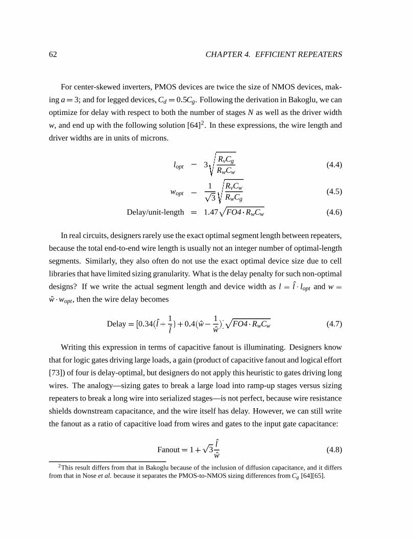
62 CHAPTER 4. EFFICIENT REPEATERS
For center-skewed inverters, PMOS devices are twice the size of NMOS devices, mak-
ing a 3; and for legged devices, Cd 0 5Cg. Following the derivation in Bakoglu, we can
optimize for delay with respect to both the number of stages N as well as the driver width
w, and end up with the following solution [64]2. In these expressions, the wire length and
driver widths are in units of microns.
lopt 3
RvCg
RwCw(4.4)
wopt
1
3
RvCw
RwCg(4.5)
Delay/unit-length 1 47
FO4 RwCw (4.6)
In real circuits, designers rarely use the exact optimal segment length between repeaters,
because the total end-to-end wire length is usually not an integer number of optimal-length
segments. Similarly, they also often do not use the exact optimal device size due to cell
libraries that have limited sizing granularity. What is the delay penalty for such non-optimal
designs? If we write the actual segment length and device width as l l lopt and w
w wopt, then the wire delay becomes
Delay 0 34l
1
l
0 4 w
1w
FO4 RwCw (4.7)
Writing this expression in terms of capacitive fanout is illuminating. Designers know
that for logic gates driving large loads, a gain (product of capacitive fanout and logical effort
[73]) of four is delay-optimal, but designers do not apply this heuristic to gates driving long
wires. The analogy—sizing gates to break a large load into ramp-up stages versus sizing
repeaters to break a long wire into serialized stages—is not perfect, because wire resistance
shields downstream capacitance, and the wire itself has delay. However, we can still write
the fanout as a ratio of capacitive load from wires and gates to the input gate capacitance:
Fanout 1 3
lw
(4.8)
2This result differs from that in Bakoglu because of the inclusion of diffusion capacitance, and it differsfrom that in Nose et al. because it separates the PMOS-to-NMOS sizing differences from Cg [64][65].

4.2. CMOS REPEATERS 63
We note that the fanout is independent of the actual technology parameters, and depends
strictly on the ratio of the segment length and driver width when normalized to their delay-
optimal values (of course, the optimal length and width are highly technology-dependent).
At optimal delay, when l w 1, the fanout is approximately 2.7. This formula points out
that sizing by selecting a ratio of l to w (i.e. the fanout) does not necessarily return useful
sizes and lengths. The fanout can remain near optimal for grossly under- or over-sized
wires and devices.
Equation 4.7 is of the form x 1
x , so the penalty for grossly undersizing w and l—either
underdriving the wires or overcrowding the wire with too many repeaters—is greater than
grossly oversizing them. However, slightly mis-sized w and l lead to only slight perfor-
mance penalties: underdriving the wires by 20% and over-spacing the repeaters by 40%
leads to only a 4% delay penalty. In Figure 4.3 we see contours corresponding to 2% delay
penalty increments as the stage length l and driver width w vary.
Delay penalty from optimal (%)
40
30
20
10
0
w wwopt
1.41.2
10.8
0.60.4l l
lopt 21.81.61.41.210.80.60.4
Figure 4.3: Delay sensitivity (2% contours)
We expect delay-optimal solutions to be inefficient. Delay optimization naturally sacri-
fices large power and energy costs in order to gain marginal delay benefits. At the optimal

64 CHAPTER 4. EFFICIENT REPEATERS
solution (l w 1), especially, the shallowness of the contours implicates only minor per-
formance gains for fairly large changes in l and w. From a design perspective, this delay
optimality is wasteful; giving up small increments of performance to save energy leads to
far better designs. In order to quantify gains in efficiency, we next construct models for
repeater energy and optimize for energy-delay product.
4.2.2 Optimizing for energy-delay product
While a thorough energy analysis would not only consider switched capacitive current but
also device leakage and crowbar (rush-through) current, this discussion will focus primarily
on switched capacitances and ignore leakage currents, which are today an insignificant
portion of total current. Crowbar currents will be approximated by a fixed multiplicative
factor.
Simply adding up the various switched capacitances gives us the total switching energy
below, where c represents a crowbar multiplier and L is the total wire length.
Etot CwLV 2
1 4 5
3 3c
w
l (4.9)
Combining this result with the previous delay expression gives us the contours shown below
in Figure 4.4 (using a crowbar of 1). The straight lines are 5% energy contours from the
minimal-delay solution; there is no practical real “minimal-energy” solution outside of not
doing the design. This picture helps to quantify the inefficiencies of a delay-centric design.
For example, even within the first delay contour, when l and w are close enough to 1 to
be within 2% of the delay optimum, the energy costs can swing by more than 15%. If, as
suggested above, we set l 1 4 and w 0 8 and accept a 4% performance penalty, we can
save 20% of the consumed energy.
The contours shown below in Figure 4.5 illustrate the optimal l and w for product of
energy and delay. This graph arises from optimizing the products of Equation 4.7 and
Equation 4.9, and in it, the benefits of longer wire segments and smaller drivers are clear.
At the energy delay minimum, when l 1 59 and w 0 62, the system has a constant
fanout of 5.44, a delay of 11.5% worse than at the delay-optimal, and an energy of 28.4%
better than that at the delay-optimal.
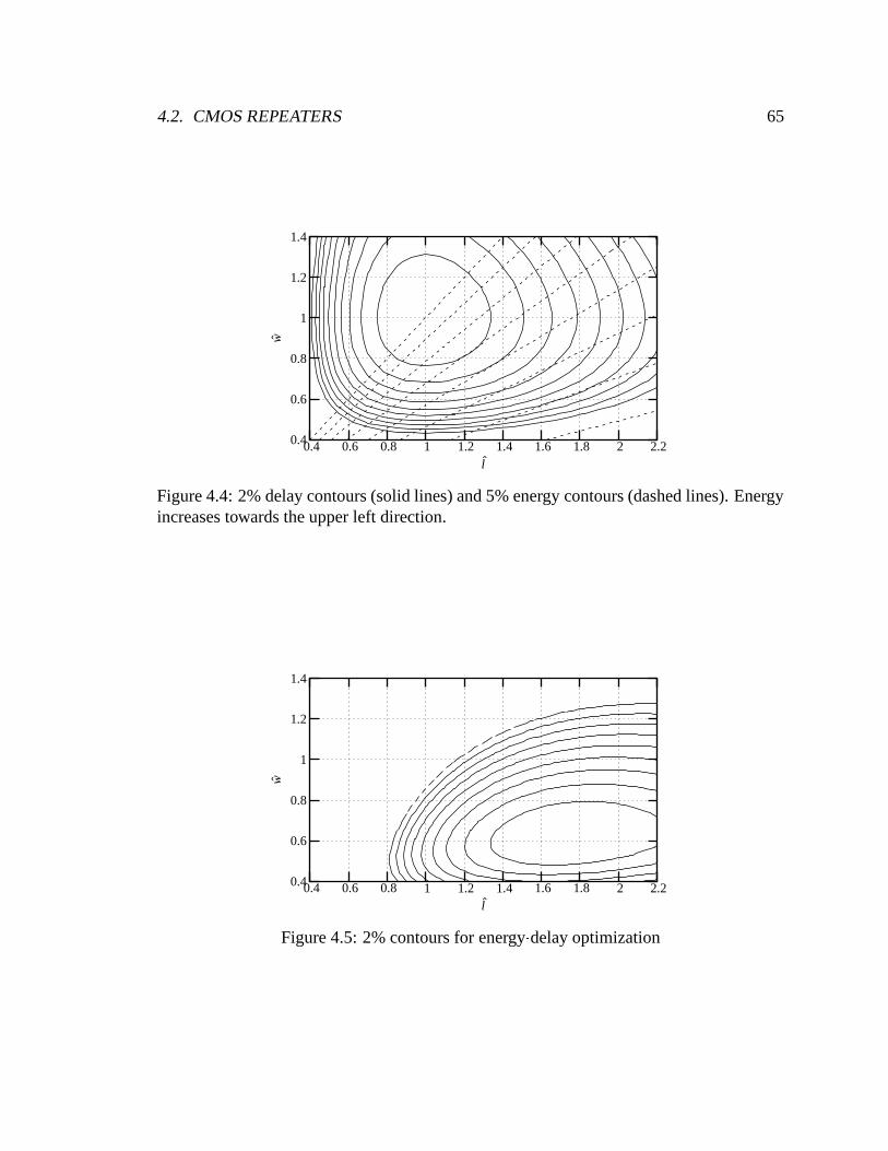
4.2. CMOS REPEATERS 65
l
w
2.221.81.61.41.210.80.60.4
1.4
1.2
1
0.8
0.6
0.4
Figure 4.4: 2% delay contours (solid lines) and 5% energy contours (dashed lines). Energyincreases towards the upper left direction.
l
w
2.221.81.61.41.210.80.60.4
1.4
1.2
1
0.8
0.6
0.4
Figure 4.5: 2% contours for energy delay optimization
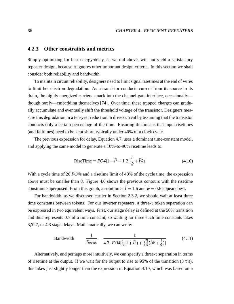
66 CHAPTER 4. EFFICIENT REPEATERS
4.2.3 Other constraints and metrics
Simply optimizing for best energy delay, as we did above, will not yield a satisfactory
repeater design, because it ignores other important design criteria. In this section we shall
consider both reliability and bandwidth.
To maintain circuit reliability, designers need to limit signal risetimes at the end of wires
to limit hot-electron degradation. As a transistor conducts current from its source to its
drain, the highly energized carriers smack into the channel-gate interface, occasionally—
though rarely—embedding themselves [74]. Over time, these trapped charges can gradu-
ally accumulate and eventually shift the threshold voltage of the transistor. Designers mea-
sure this degradation in a ten-year reduction in drive current by assuming that the transistor
conducts only a certain percentage of the time. Ensuring this means that input risetimes
(and falltimes) need to be kept short, typically under 40% of a clock cycle.
The previous expression for delay, Equation 4.7, uses a dominant time-constant model,
and applying the same model to generate a 10%-to-90% risetime leads to:
RiseTime FO4 1 l2
1 2 lw
lw (4.10)
With a cycle time of 20 FO4s and a risetime limit of 40% of the cycle time, the expression
above must be smaller than 8. Figure 4.6 shows the previous contours with the risetime
constraint superposed. From this graph, a solution at l 1 6 and w 0 6 appears best.
For bandwidth, as we discussed earlier in Section 2.3.2, we should wait at least three
time constants between tokens. For our inverter repeaters, a three-τ token separation can
be expressed in two equivalent ways. First, our stage delay is defined at the 50% transition
and thus represents 0.7 of a time constant, so waiting for three such time constants takes
30 7, or 4.3 stage delays. Mathematically, we can write:
Bandwidth 1
Trepeat
1
4 3 FO4 13
1
l2
3
4 5
lw
lw
(4.11)
Alternatively, and perhaps more intuitively, we can specify a three-τ separation in terms
of risetime at the output. If we wait for the output to rise to 95% of the transition (3 τ’s),
this takes just slightly longer than the expression in Equation 4.10, which was based on a
4.2. CMOS REPEATERS 67
l
w
2.221.81.61.41.210.80.60.4
1.4
1.2
1
0.8
0.6
0.4
Figure 4.6: 2% contours for energy delay optimization with risetime constraint
10% to 90% transition, or 2.2 τ’s. Scaling the previous risetime expression by 32 2 gives
an expression identical to that in Equation 4.11.
Notably, these expressions for repeat time do not depend on the wire parameters Rw
and Cw. A repeated wire with skinny, high-resistance wires will have the same stage delay
as one with fat, low-resistance wires. Of course, the low-resistance wires will have stages
at farther intervals, so that more territory is covered per stage, leading to a faster wire with
lower delay. However, for systems that are latency insensitive but which require high band-
width, designers ought not engineer wires for better RC performance, but should instead
maximally pack them for best density.
Finally, we note that optimizing for an energy bandwidth product would be uninterest-
ing. Peak bandwidth comes from extremely short stage delays, so that the best bandwidth
would come from stacking tiny inverter after tiny inverter, end upon end, with very little
wire between stages. The energy cost of such a silly system would be large but offset by
the gains in bandwidth. Adding a cost function for area (or equivalently, via utilization
in “diving” down to the substrate from the wire layer) would make such a model more
realistic.
To conclude this discussion of inverter repeaters, we list our figures of merit for the
purely delay-optimal solution, compared to the energy delay optimum (under a risetime
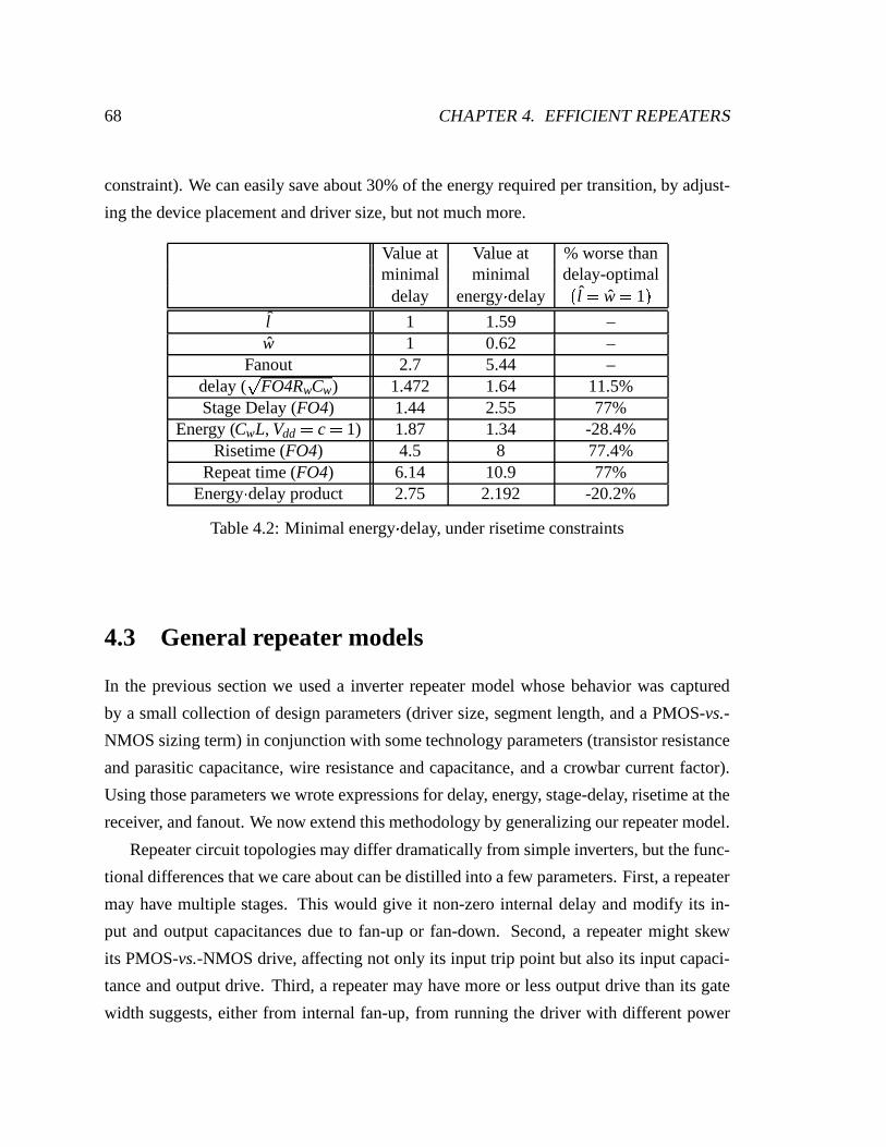
68 CHAPTER 4. EFFICIENT REPEATERS
constraint). We can easily save about 30% of the energy required per transition, by adjust-
ing the device placement and driver size, but not much more.
Value at Value at % worse thanminimal minimal delay-optimal
delay energy delayl w 1
l 1 1.59 –w 1 0.62 –
Fanout 2.7 5.44 –delay ( FO4RwCw) 1.472 1.64 11.5%Stage Delay (FO4) 1.44 2.55 77%
Energy (CwL, Vdd c 1) 1.87 1.34 -28.4%
Risetime (FO4) 4.5 8 77.4%Repeat time (FO4) 6.14 10.9 77%
Energy delay product 2.75 2.192 -20.2%
Table 4.2: Minimal energy delay, under risetime constraints
4.3 General repeater models
In the previous section we used a inverter repeater model whose behavior was captured
by a small collection of design parameters (driver size, segment length, and a PMOS-vs.-
NMOS sizing term) in conjunction with some technology parameters (transistor resistance
and parasitic capacitance, wire resistance and capacitance, and a crowbar current factor).
Using those parameters we wrote expressions for delay, energy, stage-delay, risetime at the
receiver, and fanout. We now extend this methodology by generalizing our repeater model.
Repeater circuit topologies may differ dramatically from simple inverters, but the func-
tional differences that we care about can be distilled into a few parameters. First, a repeater
may have multiple stages. This would give it non-zero internal delay and modify its in-
put and output capacitances due to fan-up or fan-down. Second, a repeater might skew
its PMOS-vs.-NMOS drive, affecting not only its input trip point but also its input capaci-
tance and output drive. Third, a repeater may have more or less output drive than its gate
width suggests, either from internal fan-up, from running the driver with different power
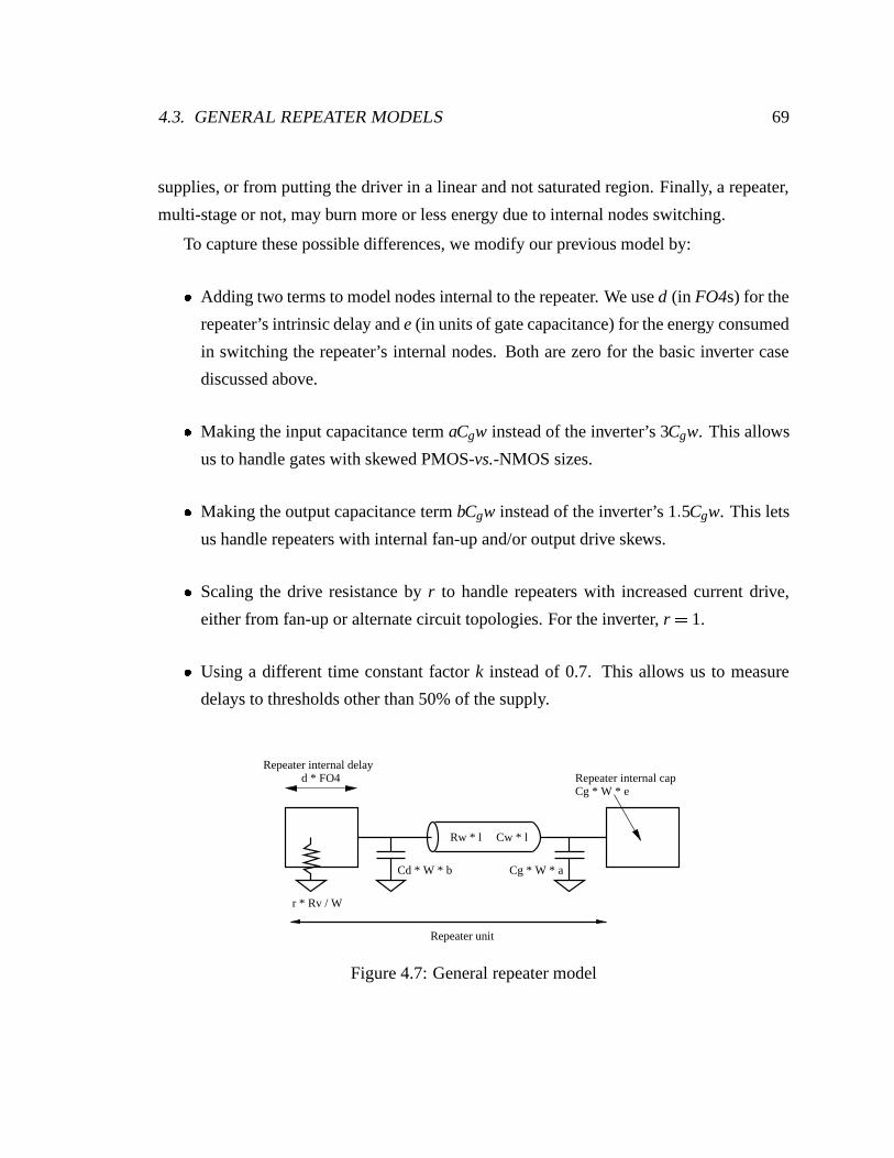
4.3. GENERAL REPEATER MODELS 69
supplies, or from putting the driver in a linear and not saturated region. Finally, a repeater,
multi-stage or not, may burn more or less energy due to internal nodes switching.
To capture these possible differences, we modify our previous model by:
Adding two terms to model nodes internal to the repeater. We use d (in FO4s) for the
repeater’s intrinsic delay and e (in units of gate capacitance) for the energy consumed
in switching the repeater’s internal nodes. Both are zero for the basic inverter case
discussed above.
Making the input capacitance term aCgw instead of the inverter’s 3Cgw. This allows
us to handle gates with skewed PMOS-vs.-NMOS sizes.
Making the output capacitance term bCgw instead of the inverter’s 1 5Cgw. This lets
us handle repeaters with internal fan-up and/or output drive skews.
Scaling the drive resistance by r to handle repeaters with increased current drive,
either from fan-up or alternate circuit topologies. For the inverter, r 1.
Using a different time constant factor k instead of 0.7. This allows us to measure
delays to thresholds other than 50% of the supply.
d * FO4Repeater internal delay
Rw * l Cw * l
Cg * W * a
Repeater unit
Cd * W * b
r * Rv / W
Cg * W * eRepeater internal cap
Figure 4.7: General repeater model
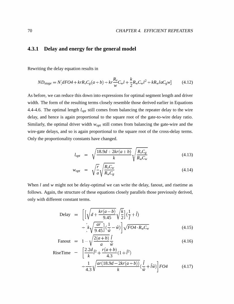
70 CHAPTER 4. EFFICIENT REPEATERS
4.3.1 Delay and energy for the general model
Rewriting the delay equation results in
NDstage N dFO4
krRvCg
a
b
krRv
wCwl
k2
RwCwl2 kRwlaCgw (4.12)
As before, we can reduce this down into expressions for optimal segment length and driver
width. The form of the resulting terms closely resemble those derived earlier in Equations
4.4-4.6. The optimal length lopt still comes from balancing the repeater delay to the wire
delay, and hence is again proportional to the square root of the gate-to-wire delay ratio.
Similarly, the optimal driver width wopt still comes from balancing the gate-wire and the
wire-gate delays, and so is again proportional to the square root of the cross-delay terms.
Only the proportionality constants have changed.
lopt
18 9d
2kr
a
b
k
RvCg
RwCw(4.13)
wopt
ra
RvCw
RwCg(4.14)
When l and w might not be delay-optimal we can write the delay, fanout, and risetime as
follows. Again, the structure of these equations closely parallels those previously derived,
only with different constant terms.
Delay
d
kra
b
9 45
k2 1
l
l
k ar
9 45 1
w
w FO4 RwCw (4.15)
Fanout 1
2a
b
alw
(4.16)
RiseTime
2 2d
kl2 r
a
b
4 31
l2
14 3
ar
18 9d
2kr
a
b
k
lw
lw FO4 (4.17)

4.4. EXAMPLES OF REPEATER OPTIMIZATIONS 71
As before we can also write an expression for bandwidth (or repeat-time). In the previ-
ous section we derived a lower-bound for repeat-time based on stage delay. But here, with
an internal delay in the repeater, the maximum repeat time is set by the greater of the wire
“delay” (a three-τ risetime delay) and the internal repeater delay. However, because the
wire delay always exceeds the internal repeater delay, we can simply write repeat-time as
a multiple of the risetime above.
Notice that the signal risetime is proportional to the repeater’s internal delay, as written
above in Equation 4.17. This makes sense because the inter-repeater segment length tracks
the repeater’s internal delay: the slower the repeater, the longer the wire between repeaters,
and hence the slower the risetime.
4.4 Examples of repeater optimizations
The advantage of the general model formulation is that we can easily compare alternative
repeater topologies and examine their sizing and placement from a delay and energy delay
perspective. We will see that buffers and tristate repeaters require a small penalty in return
for ease of placement (buffers) and some reconfigurability (tristates).
4.4.1 Example: Buffers
Buffers, or back-to-back inverters, may be used as repeaters to simplify the design of long
interconnects, because they avoid logic inversions along the wire. Inserting an odd number
of buffer repeaters causes no logic problems. However, they are slightly less efficient.
We assume the internal fanout inside the buffer to be 2.5; this provides for a good
energy delay minimum (see Appendix). This makes our parameters:
a 3: PMOS devices are twice the size of NMOS devices.
b 3 75: At Cd 0 5Cg, the buffer has a fanout of 2.5.
r 0 4: The output current drive is 2.5 times stronger.
d 0 66: At Cd 0 5Cg, a FO2.5 is 3
4 5 times a FO4.

72 CHAPTER 4. EFFICIENT REPEATERS
e 9: Internal load is Cdw of first stage plus 2 5Cgw of the second.
k 0 7: We still use the 50% transition point for delay.
We can now plug these terms into our model and turn the crank. The delay-optimal stage
length and driver width are
lopt 4 8 RvCg
RwCw(4.18)
wopt 0 36
RvCw
RwCg(4.19)
Delay 0 551l
1
l
0 249w
1w
FO4 RwCw (4.20)
Dstage FO4 0 867
1
l2
0 393lw
lw
(4.21)
Compared to the inverter case, the length sensitivity is greater but the width sensitivity
smaller. Because the buffer has internal delay, the optimal inter-stage wire length is longer,
and hence varying the actual length has a greater effect due to its l2 term.
At the delay-optimal design point l w 1, we get a delay of 1 6 FO4 RwCw and a
stage delay of 2.518FO4s. This delay is 8.7% worse than at the inverter’s delay-optimal.
The risetime at the receiver input, in FO4s, becomes
RT 2 095l2 0 628
1
l2
1 232 lw
lw (4.22)
or 5.8 FO4s at l w 1, and the repeat time follows directly. The risetime constraint,
superposed onto the delay contours in Figure 4.8 below, is much tighter than with inverters.
The energy consumed by the buffer is
Etot CwLV 2
dd 1 1 189c
w
l (4.23)
or 2.189 CwLV 2 at l w c 1.
Figure 4.8 shows first the delay contours with a rise-time constraint. Figure 4.9 does
the same, only with energy delay contours. Because the minimal delay-energy solution
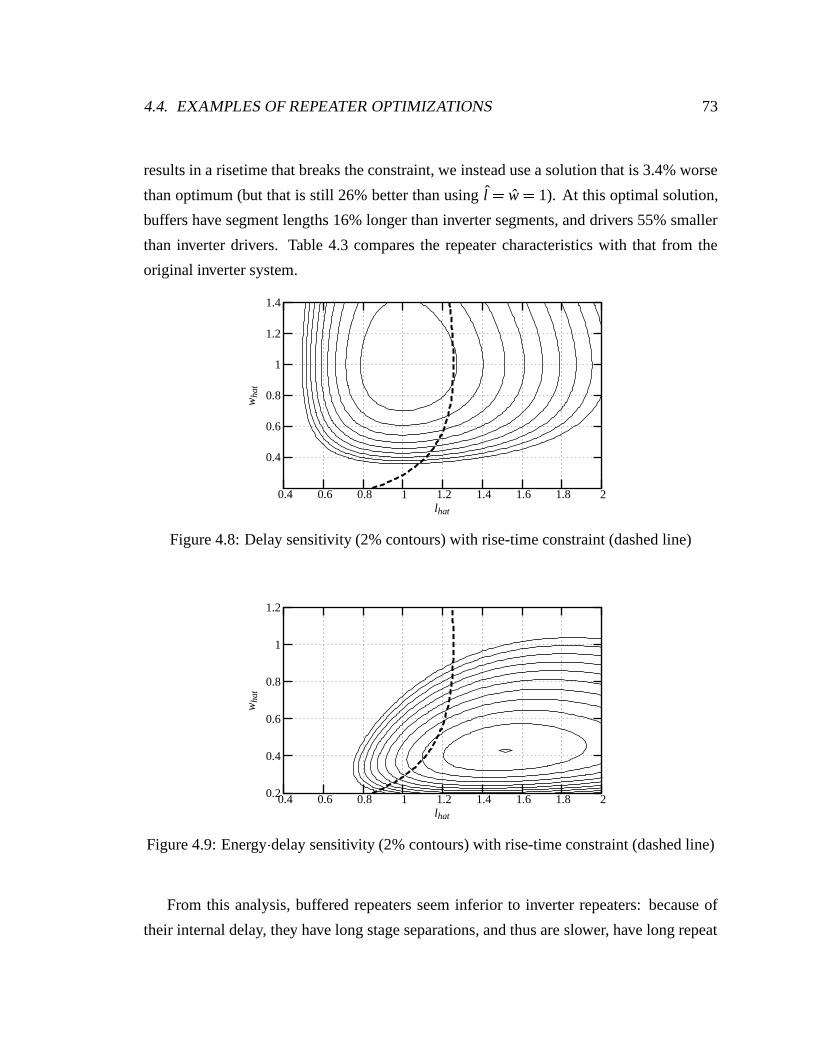
4.4. EXAMPLES OF REPEATER OPTIMIZATIONS 73
results in a risetime that breaks the constraint, we instead use a solution that is 3.4% worse
than optimum (but that is still 26% better than using l w 1). At this optimal solution,
buffers have segment lengths 16% longer than inverter segments, and drivers 55% smaller
than inverter drivers. Table 4.3 compares the repeater characteristics with that from the
original inverter system.
lhat
wha
t
21.81.61.41.210.80.60.4
1.4
1.2
1
0.8
0.6
0.4
Figure 4.8: Delay sensitivity (2% contours) with rise-time constraint (dashed line)
lhat
wha
t
21.81.61.41.210.80.60.4
1.2
1
0.8
0.6
0.4
0.2
Figure 4.9: Energy delay sensitivity (2% contours) with rise-time constraint (dashed line)
From this analysis, buffered repeaters seem inferior to inverter repeaters: because of
their internal delay, they have long stage separations, and thus are slower, have long repeat

74 CHAPTER 4. EFFICIENT REPEATERS
% worse than % worse thanValue delay-optimal inverters
l w 1 (E D min)
l 1.141 – (16% longer)w 0.437 – (55% smaller)
Fanout 6.5 – –Delay ( FO4 RwCw) 1.791 11.9% 9.1%
Stage Delay (FO4) 3.214 27.6% 26%Energy (CwL, Vdd
c 1) 1.456 -33% 9%Risetime (FO4) 8 14% 0%
Repeat time (FO4) 10.9 14% 0%Energy delay product 2.607 -25.6% 18.9%
Table 4.3: Buffer minimal energy delay, under risetime constraints
times, and burn more energy. However, buffered repeaters are still popular on micropro-
cessor designs (or other large designs with irregular wiring patterns), because they preserve
logic levels. This makes buffered repeaters ideal for back-end timing-driven repeater inser-
tion, while inverter repeaters require the designer to beware of an odd number of repeating
stages.
Another reason often cited for the continued use of buffered repeaters is lower crowbar
current. With inverter repeaters, each stage is large and sees a relatively slow input slew,
leading to significant crowbar current (the c term is nontrivial). With buffered repeaters,
the small leading stage sees a slow input slew while the large trailing stage sees a fast
input slew. This means that the trailing stage’s c term is smaller than the leading stage’s,
a detail ignored by the previous analysis. This effect is small, however: if we assume a
crowbar factor of 1.25 for the slow-slewing input and 1.05 for the fast-slewing input, then
accounting for this effect at l 1 045 and w 0 435 leads to a difference of under 5% in
consumed energy.
4.4.2 Example 2: Tristates
Tristate repeaters offer simple wire programmability. A simple NEWS set of repeaters al-
lows for a signal to travel in each of four directions, as shown in the figure below. This
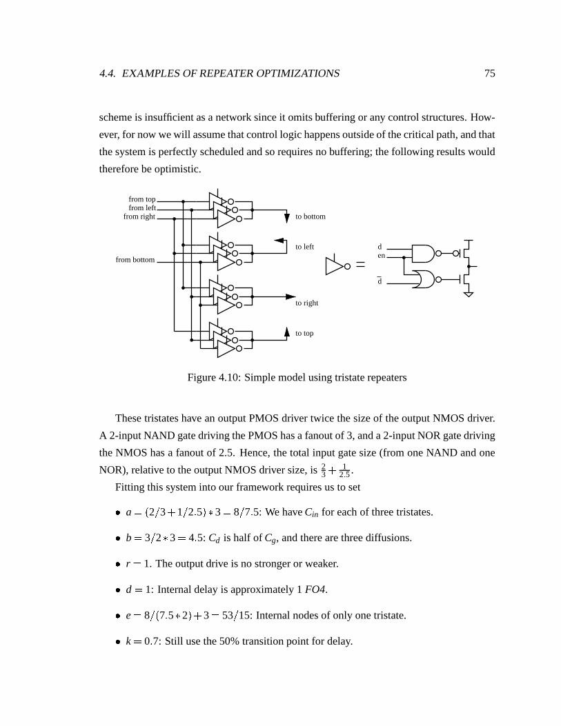
4.4. EXAMPLES OF REPEATER OPTIMIZATIONS 75
scheme is insufficient as a network since it omits buffering or any control structures. How-
ever, for now we will assume that control logic happens outside of the critical path, and that
the system is perfectly scheduled and so requires no buffering; the following results would
therefore be optimistic.
from top
from bottom
from leftfrom right to bottom
to top
to right
to left den
d
Figure 4.10: Simple model using tristate repeaters
These tristates have an output PMOS driver twice the size of the output NMOS driver.
A 2-input NAND gate driving the PMOS has a fanout of 3, and a 2-input NOR gate driving
the NMOS has a fanout of 2.5. Hence, the total input gate size (from one NAND and one
NOR), relative to the output NMOS driver size, is 23
12 5 .
Fitting this system into our framework requires us to set
a
23
12 5 3 8
7 5: We have Cin for each of three tristates.
b 32 3 4 5: Cd is half of Cg, and there are three diffusions.
r 1. The output drive is no stronger or weaker.
d 1: Internal delay is approximately 1 FO4.
e 8
7 5 2 3 53
15: Internal nodes of only one tristate.
k 0 7: Still use the 50% transition point for delay.
76 CHAPTER 4. EFFICIENT REPEATERS
These parameters result in the following expressions for stage length, driver width, and
delays:
lopt 6 5 RvCg
RwCw(4.24)
wopt 0 56
RvCw
RwCg(4.25)
Delay 0 741l
1
l
0 407w
1w
FO4 RwCw (4.26)
Dstage FO4 1 570
1
l2
0 863lw
lw
(4.27)
The delay-optimal length and l sensitivity term is twice that of the inverter case, while
the width and w term about the same. The delay-optimal delay is 2.297, or 56% longer than
the inverter’s delay.
Because the tristate repeaters have relatively low current drive for the load they drive,
the risetime constraint presents problems. We can write the risetime as
RT 3 143l2 1 791
1
l2
2 709 lw
lw (4.28)
and see that at the delay-optimal point, the risetime at the receiver is 12.1 FO4s, which
violates our 8 FO4 constraint. Instead of using l w 1, our baseline needs to be at
l 0 7 and w 1, which makes the risetime 8 FO4s. Doing this invokes a delay penalty
of 4% and an energy penalty of 21%.
Energy consumed by the tristate repeaters is 1.964 CwLV 2 at l w c 1.
Etot CwLV 2
dd 1 0 964c
w
l (4.29)
As before we minimize the delay-energy product, and show the results in the following
table and graphs. These contours are now at 4% steps. The minimal delay energy is far
from the risetime curve, so that we need to pick a design point that leaves considerable
performance on the table: at l 0 633 and w 0 51 the delay-energy product is 4% worse
than at the delay-optimal and 35.6% worse than at the delay-energy minimum points. Also,

4.4. EXAMPLES OF REPEATER OPTIMIZATIONS 77
at this design point, the segment length is 14% shorter than the inverter’s design point, and
the driver width 20% smaller.
% worse than % worse thanValue delay-optimal inverters
l w 1 (E D min)
l 0.633 – (14% shorter)w 0.510 – (20% smaller)
Fanout 3.726 – –Delay ( FO4RwCw) 2.648 15.3% 61%Stage Delay (FO4) 3.548 -27.1% 39%
Energy (CwL, Vdd c 1) 1.777 -9.5% 33%
Risetime (FO4) 8 14% 0%Repeat time (FO4) 10.9 14% 0%
Energy delay product 4.705 4.26% 114.6%
Table 4.4: Minimal energy delay, under risetime constraints
lhat
wha
t
21.81.61.41.210.80.60.4
1.2
1
0.8
0.6
0.4
Figure 4.11: Delay sensitivity (4% contours) with rise-time constraint (dashed line)
This analysis reflects the costs of some primitive reconfigurability in wires. If we
wanted to replace a regular grid of inverter repeaters with tristates for more flexible rout-
ing, we would need to shorten the segments and make the overall device sizes smaller. The
resulting system would have moderately worse performance than inverters but have much
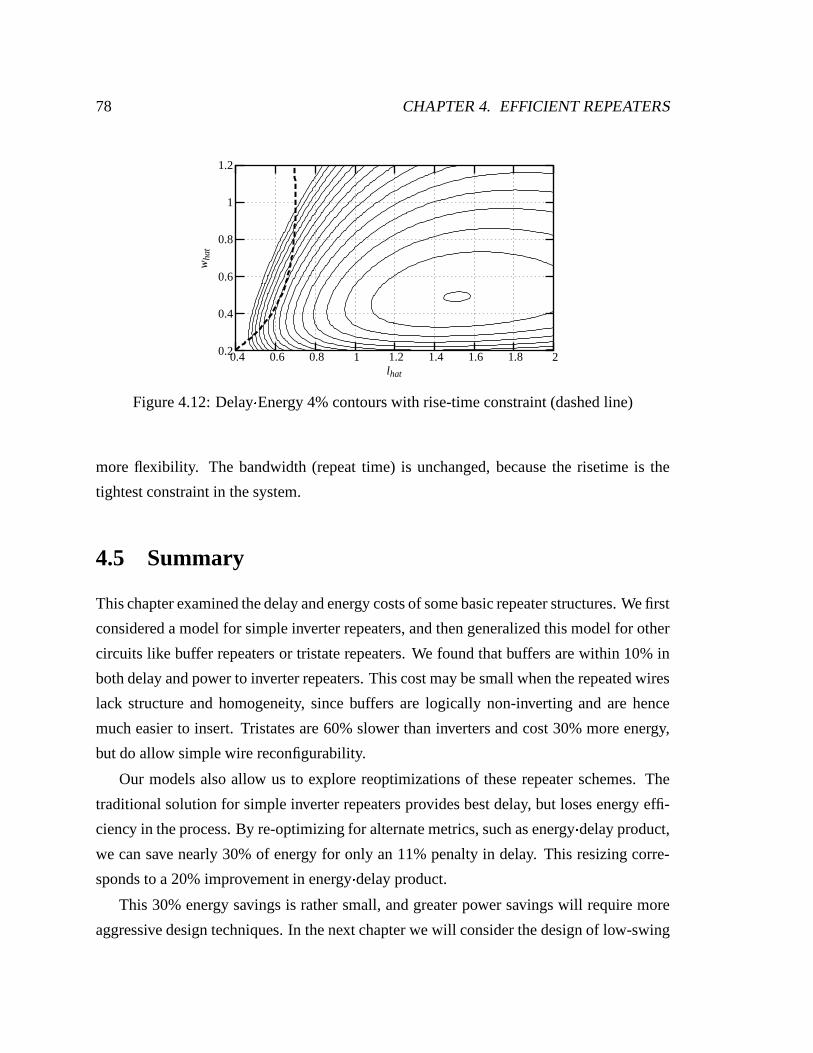
78 CHAPTER 4. EFFICIENT REPEATERS
lhat
wha
t
21.81.61.41.210.80.60.4
1.2
1
0.8
0.6
0.4
0.2
Figure 4.12: Delay Energy 4% contours with rise-time constraint (dashed line)
more flexibility. The bandwidth (repeat time) is unchanged, because the risetime is the
tightest constraint in the system.
4.5 Summary
This chapter examined the delay and energy costs of some basic repeater structures. We first
considered a model for simple inverter repeaters, and then generalized this model for other
circuits like buffer repeaters or tristate repeaters. We found that buffers are within 10% in
both delay and power to inverter repeaters. This cost may be small when the repeated wires
lack structure and homogeneity, since buffers are logically non-inverting and are hence
much easier to insert. Tristates are 60% slower than inverters and cost 30% more energy,
but do allow simple wire reconfigurability.
Our models also allow us to explore reoptimizations of these repeater schemes. The
traditional solution for simple inverter repeaters provides best delay, but loses energy effi-
ciency in the process. By re-optimizing for alternate metrics, such as energy delay product,
we can save nearly 30% of energy for only an 11% penalty in delay. This resizing corre-
sponds to a 20% improvement in energy delay product.
This 30% energy savings is rather small, and greater power savings will require more
aggressive design techniques. In the next chapter we will consider the design of low-swing
4.5. SUMMARY 79
circuits, which hold the promise of power-savings much larger than those available from
simple resizing.

Chapter 5
Low-Swing Repeaters
In the previous chapter we considered local optimizations on repeated wires by varying seg-
ment length and repeater driver width in order to make them more energy-efficient. This is
akin to trying to save fuel by driving a Cadillac with the air conditioner turned off: the un-
derlying vehicle’s inefficiencies still dominate. In addition, reliance upon repeater schemes
to overcome wire resisitance leads to layout and via congestion. The Smart Memories mod-
ular architecture has 128-bit, 4.5mm long links between module cores and, as shown in the
previous chapter, would need four repeater stations along the links. Each repeater station
would need 128 holes drilled down and then back up through all intermediate wiring layers,
as well as a channel for 128 large inverters. While the area cost of the inverters, relative
to the total die, lessens with technology scaling, the via and wire congestion costs remain
high, significantly complicating physical design.
This chapter discusses how using low-voltage signaling effectively reduces energy con-
sumption, and, if used to drive each Smart Memories link in a single stage, avoids the
physical design complications of multiple repeater stages.
5.1 Benefits and costs of low-swing signaling
Reducing the voltage swing of our global interconnects linearly reduces the required en-
ergy, because capacitors need swing only a fraction of the original voltage. In addition,
if we can provide the charge from an additional reduced power supply, then we can gain
80
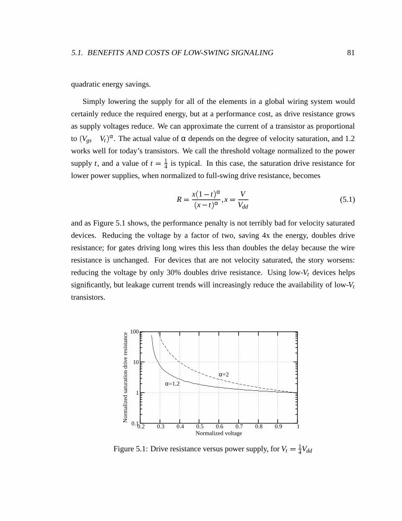
5.1. BENEFITS AND COSTS OF LOW-SWING SIGNALING 81
quadratic energy savings.
Simply lowering the supply for all of the elements in a global wiring system would
certainly reduce the required energy, but at a performance cost, as drive resistance grows
as supply voltages reduce. We can approximate the current of a transistor as proportional
toVgs Vt α. The actual value of α depends on the degree of velocity saturation, and 1.2
works well for today’s transistors. We call the threshold voltage normalized to the power
supply t, and a value of t 14 is typical. In this case, the saturation drive resistance for
lower power supplies, when normalized to full-swing drive resistance, becomes
R x1 t α
x t α x
VVdd
(5.1)
and as Figure 5.1 shows, the performance penalty is not terribly bad for velocity saturated
devices. Reducing the voltage by a factor of two, saving 4x the energy, doubles drive
resistance; for gates driving long wires this less than doubles the delay because the wire
resistance is unchanged. For devices that are not velocity saturated, the story worsens:
reducing the voltage by only 30% doubles drive resistance. Using low-Vt devices helps
significantly, but leakage current trends will increasingly reduce the availability of low-Vt
transistors.
α=1.2
α=2
Normalized voltage
Nor
mal
ized
satu
rati
ondr
ive
resi
stan
ce
10.90.80.70.60.50.40.30.2
100
10
1
0.1
Figure 5.1: Drive resistance versus power supply, for Vt 1
4Vdd

82 CHAPTER 5. LOW-SWING REPEATERS
While this wholesale voltage reduction would certainly improve the energy-delay prod-
uct, lowering the voltage swing and supply for only the long wires of a global interconnect
system would do significantly more. It would maintain large energy savings: the long wires
between repeater stations represent much of the capacitance in the system. But keeping full
voltage swing for the logic stages leading up to the wire drivers retains high gate overdrive
voltage, thus maintaining low drive resistance and high speed.
Using such a low-swing system, and designing it to drive the 4.5mm global intercon-
nects of the Smart Memories chip in a single stage, would solve both power and layout
congestion problems. It would also introduce a host of new issues, including how to strobe
the receivers to tell them when to look at the data, and how to minimize the effects of noise
that corrupts data.
However, we can turn the characteristics of the Smart Memories global interconnection
network to our advantage and exploit them to simplify our problem. The homogeneity of
the global fabric allows a fixed latency for all point-to-point connections, making a clocked
receiver feasible and inexpensive. Also, because each link needs only to fit within a clock
phase, the timing of each link can be relaxed somewhat and not squeezed to obtain minimal
delay. In this case, a small timing overhead for the clocking of the driver and receiver is
not only possible but in fact harmless to overall system performance. Finally, the regularity
and structure of the global network means that wire environments are stable and well-
characterized, making them well-suited for sensitive circuits like low-swing wires.
This chapter will outline a low-swing system suitable for the Smart Memories global
network and focus on its component parts in depth. A sample design of this low-swing
system, set for a contemporary 0.18-µm technology, elucidates some of the engineering
tradeoffs. This design emulates the target Smart Memories fabric: 10mm wires in a 0.18-
µm technology have the same resistance, although higher capacitance, than 4.5mm wires
in a 0.10-µm technology. The system is designed to run at an aggressive repeat rate of 10
FO4s, matching the target system speed of the Smart Memories machine.

5.2. LOW-SWING REPEATER SYSTEMS 83
5.2 Low-swing repeater systems
A low-swing repeated-wire system, simplified in Figure 5.2, contains three parts. First, a
low-swing transmitter using overdrive and distributed equalization for higher performance
transmits a signal down a long wire. Second, the wires that carry this signal are differential
and twisted to reduce noise effects. Third, a clocked regenerative amplifier receives the
signal and converts it to full-swing levels suitable for logical operations such as queueing
or arbitration.
Vdd
Gnd
Transmitter
Bit
Φ
Receiver
Equalizer circuits
Bit
10mm twisted, differential wires
Figure 5.2: Generic low-swing repeated wire
5.2.1 Low-swing transmitter circuits
The transmitter circuits used in this low-swing system use a number of techniques to com-
municate quickly over long distances, including pre-emphasis, pre-equalization, and linear
drive resistance. First we discuss how to limit voltage swing on the global wires.
Restricting swing
In our proposed system we rely on a separate reduced power supply for increased energy
efficiency [75]. This is a minor cheat: it removes complexity from the transmitter circuit,
because voltage generation becomes free, and adds complexity to the power grid design.
Although extra grids may require more layout work, they are certainly feasible. Power
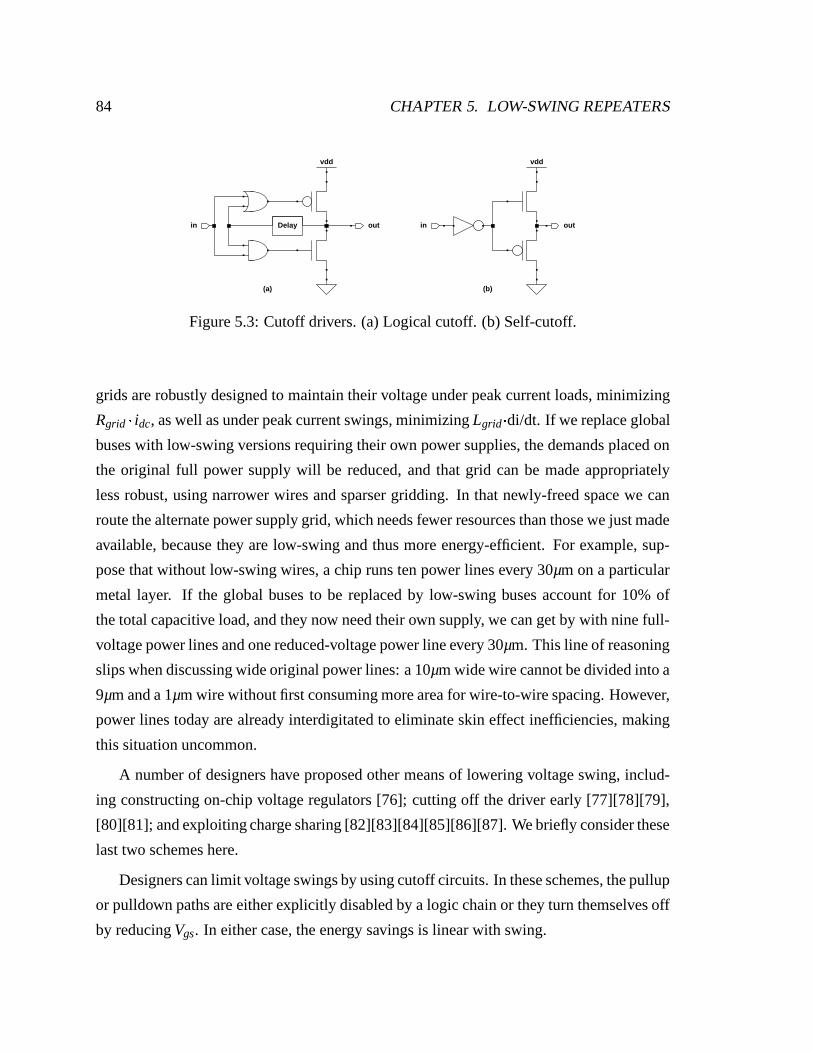
84 CHAPTER 5. LOW-SWING REPEATERS
vdd
outin Delay
vdd
in out
(a) (b)
Figure 5.3: Cutoff drivers. (a) Logical cutoff. (b) Self-cutoff.
grids are robustly designed to maintain their voltage under peak current loads, minimizing
Rgrid idc, as well as under peak current swings, minimizing Lgrid di/dt. If we replace global
buses with low-swing versions requiring their own power supplies, the demands placed on
the original full power supply will be reduced, and that grid can be made appropriately
less robust, using narrower wires and sparser gridding. In that newly-freed space we can
route the alternate power supply grid, which needs fewer resources than those we just made
available, because they are low-swing and thus more energy-efficient. For example, sup-
pose that without low-swing wires, a chip runs ten power lines every 30µm on a particular
metal layer. If the global buses to be replaced by low-swing buses account for 10% of
the total capacitive load, and they now need their own supply, we can get by with nine full-
voltage power lines and one reduced-voltage power line every 30µm. This line of reasoning
slips when discussing wide original power lines: a 10µm wide wire cannot be divided into a
9µm and a 1µm wire without first consuming more area for wire-to-wire spacing. However,
power lines today are already interdigitated to eliminate skin effect inefficiencies, making
this situation uncommon.
A number of designers have proposed other means of lowering voltage swing, includ-
ing constructing on-chip voltage regulators [76]; cutting off the driver early [77][78][79],
[80][81]; and exploiting charge sharing [82][83][84][85][86][87]. We briefly consider these
last two schemes here.
Designers can limit voltage swings by using cutoff circuits. In these schemes, the pullup
or pulldown paths are either explicitly disabled by a logic chain or they turn themselves off
by reducing Vgs. In either case, the energy savings is linear with swing.
5.2. LOW-SWING REPEATER SYSTEMS 85
Logical cutoff drivers use local feedback from the output of the driver to trip a logic
path back to the driver’s enable, as in Figure 5.3a. Once the output has gone “far enough,”
the driver is disabled and the output line left to float at its intended voltage [77][78]. To
decide whether or not the output has indeed gone far enough, the driver can either use a
replica of the receiver or simply “dead-reckon” the transmission with a local delay.
In the first case, when the driver uses a local copy of the receiver to measure the wire
swing, a problem may arise from line resistance. Because the wire itself has intrinsic delay,
using the “near-end” voltage at the driver as a proxy for the “far-end” voltage at the receiver
can lead to timing errors and cutting off the driver too early. The second case, using a dead-
reckoned delay, is simpler, especially for homogenous and regular modular global wires
that all have the same nominal delays.
In either case, cutoff circuits suffer from noise sensitivity. The driver stops driving once
cut off, giving the signals little immunity to injected currents from other wires. In the noise
framework of the previous chapters, the victim time constant becomes infinite, maximizing
coupled noise. Engineering this noise demands increased wire-to-wire spacing, adding
some area overhead.
Logical cutoff circuits are used in specialized circuits, like in memory arrays with small
memory cells weakly pulling down bitlines. A timing signal cuts off the bitline drive once
they get pulled down part-way, saving both delay and power. However, memory array
bitlines are much shorter than repeated wire segments, and by the time their drive cuts off,
the bitline sense-amps have already fired. Thus the bitline exposure to noise, both physical
and temporal, is minimal. More importantly, the timing of their cutoff signal comes from a
replicated memory path, which matches wire delays to wire delays and gate delays to gate
delays, resulting in far closer delay matching than in the logical cutoff circuits.
The second type of cutoff driver stops itself when Vgs falls below Vt . Figure 5.3b shows
an example [79]; a variant, not shown in the figure, restricts the pullup by adding an NMOS
transistor in series with the pullup PMOS [81]. Poor performance cripples these drivers.
An NMOS device pulling down maintains a good drive resistance all the way to the bot-
tom, and this drive resistance actually improves as the device becomes linear. An NMOS
device pulling up, by contrast, has a drive resistance that approaches infinity as the device
gradually turns itself off, resulting in extremely long tails on the voltage waveforms and
86 CHAPTER 5. LOW-SWING REPEATERS
indeterminate rise- and fall-times. In addition, the high driver resistance at small Vds means
that small noise disturbances will not be restored. For our repeater model, the r term would
rise dramatically, increasing delay and making the delay and risetime equations difficult to
fit.
Another way to limit driver swings uses capacitive charge-sharing, in which the load
capacitance connects to another reservoir of charge, balancing the voltages. This other
reservoir of charge may be shared among many circuits globally, predefined to be between
complementary wires in differential signaling, or shared amongst the bits in a bus.
Global charge-sharing drivers restrict voltage swing by shorting their outputs to a large
shared capacitor [84][85]. On a falling edge charge gets shunted from the output node to
the global capacitor, and on a rising edge the output node gets pulled to Vdd while the global
capacitor sheds excess charge onto a dump capacitor. Since for small swings, the dump ca-
pacitor needs to be much larger than the circuit load capacitors, which are themselves long
wires with large capacitances, these on-chip voltage regulators have a large area overhead.
Another scheme of global charge-sharing, more suited to a bus, shorts all the “0” bits
together with a large pre-discharged shared capacitor [83]. The more bits that switch, the
lower the swing. The drawback to this technique lies in the multiple common-mode levels
required of the receivers, but it does offer 1n energy savings, where n is the number of bits
in the bus.
Sharing charge between differential bits on a bus saves energy over schemes that would
otherwise switch every cycle [87][75][82]. Extending this scheme to share charge amongst
all the bits on a bus, so that each bit has a discrete range and voltage swing, offers 1n2 energy
savings [86]. As with the previous technique, however, it also requires a host of different
common-mode voltages for the receivers.
Both bus-shorting schemes trade design complexity for power supply distribution. Sim-
ply using a 1n power supply offers 1
n2 energy savings for less complexity, but it also requires
an alternate power supply to be shipped around the die.
Overdrive pre-emphasis
Inherent offsets and mismatches at the receiver determine the minimum signal that must be
delivered to it. Using a drive voltage significantly higher than this minimum level, however,
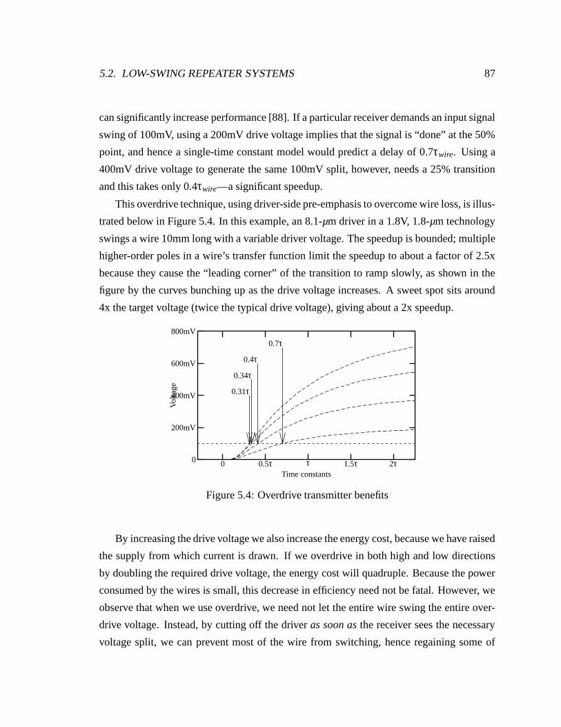
5.2. LOW-SWING REPEATER SYSTEMS 87
can significantly increase performance [88]. If a particular receiver demands an input signal
swing of 100mV, using a 200mV drive voltage implies that the signal is “done” at the 50%
point, and hence a single-time constant model would predict a delay of 0.7τwire. Using a
400mV drive voltage to generate the same 100mV split, however, needs a 25% transition
and this takes only 0.4τwire—a significant speedup.
This overdrive technique, using driver-side pre-emphasis to overcome wire loss, is illus-
trated below in Figure 5.4. In this example, an 8.1-µm driver in a 1.8V, 1.8-µm technology
swings a wire 10mm long with a variable driver voltage. The speedup is bounded; multiple
higher-order poles in a wire’s transfer function limit the speedup to about a factor of 2.5x
because they cause the “leading corner” of the transition to ramp slowly, as shown in the
figure by the curves bunching up as the drive voltage increases. A sweet spot sits around
4x the target voltage (twice the typical drive voltage), giving about a 2x speedup.
0.31τ
0.34τ
0.4τ
0.7τ
Time constants
Vol
tage
2τ1.5ττ0.5τ0
800mV
600mV
400mV
200mV
0
Figure 5.4: Overdrive transmitter benefits
By increasing the drive voltage we also increase the energy cost, because we have raised
the supply from which current is drawn. If we overdrive in both high and low directions
by doubling the required drive voltage, the energy cost will quadruple. Because the power
consumed by the wires is small, this decrease in efficiency need not be fatal. However, we
observe that when we use overdrive, we need not let the entire wire swing the entire over-
drive voltage. Instead, by cutting off the driver as soon as the receiver sees the necessary
voltage split, we can prevent most of the wire from switching, hence regaining some of
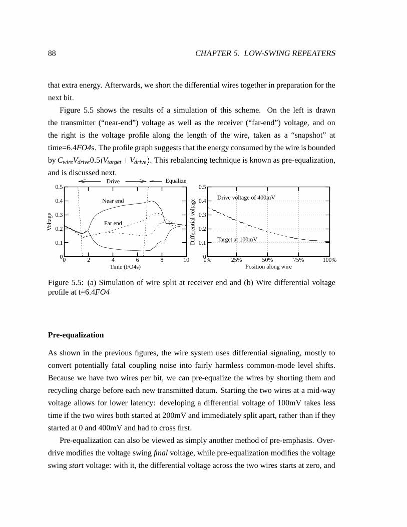
88 CHAPTER 5. LOW-SWING REPEATERS
that extra energy. Afterwards, we short the differential wires together in preparation for the
next bit.
Figure 5.5 shows the results of a simulation of this scheme. On the left is drawn
the transmitter (“near-end”) voltage as well as the receiver (“far-end”) voltage, and on
the right is the voltage profile along the length of the wire, taken as a “snapshot” at
time=6.4FO4s. The profile graph suggests that the energy consumed by the wire is bounded
by CwireVdrive0 5 Vtarget
Vdrive . This rebalancing technique is known as pre-equalization,
and is discussed next.EqualizeDrive
Far end
Near end
Time (FO4s)
Vol
tage
1086420
0.5
0.4
0.3
0.2
0.1
0
Target at 100mV
Drive voltage of 400mV
Position along wire
Dif
fere
ntia
lvol
tage
100%75%50%25%0%
0.5
0.4
0.3
0.2
0.1
0
Figure 5.5: (a) Simulation of wire split at receiver end and (b) Wire differential voltageprofile at t=6.4FO4
Pre-equalization
As shown in the previous figures, the wire system uses differential signaling, mostly to
convert potentially fatal coupling noise into fairly harmless common-mode level shifts.
Because we have two wires per bit, we can pre-equalize the wires by shorting them and
recycling charge before each new transmitted datum. Starting the two wires at a mid-way
voltage allows for lower latency: developing a differential voltage of 100mV takes less
time if the two wires both started at 200mV and immediately split apart, rather than if they
started at 0 and 400mV and had to cross first.
Pre-equalization can also be viewed as simply another method of pre-emphasis. Over-
drive modifies the voltage swing final voltage, while pre-equalization modifies the voltage
swing start voltage: with it, the differential voltage across the two wires starts at zero, and
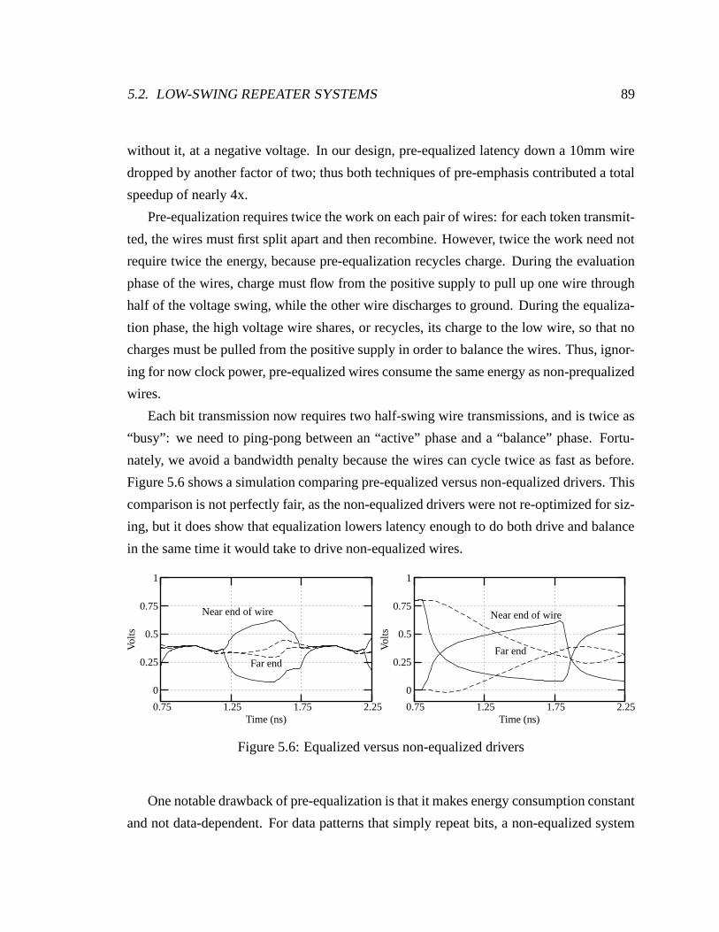
5.2. LOW-SWING REPEATER SYSTEMS 89
without it, at a negative voltage. In our design, pre-equalized latency down a 10mm wire
dropped by another factor of two; thus both techniques of pre-emphasis contributed a total
speedup of nearly 4x.
Pre-equalization requires twice the work on each pair of wires: for each token transmit-
ted, the wires must first split apart and then recombine. However, twice the work need not
require twice the energy, because pre-equalization recycles charge. During the evaluation
phase of the wires, charge must flow from the positive supply to pull up one wire through
half of the voltage swing, while the other wire discharges to ground. During the equaliza-
tion phase, the high voltage wire shares, or recycles, its charge to the low wire, so that no
charges must be pulled from the positive supply in order to balance the wires. Thus, ignor-
ing for now clock power, pre-equalized wires consume the same energy as non-prequalized
wires.
Each bit transmission now requires two half-swing wire transmissions, and is twice as
“busy”: we need to ping-pong between an “active” phase and a “balance” phase. Fortu-
nately, we avoid a bandwidth penalty because the wires can cycle twice as fast as before.
Figure 5.6 shows a simulation comparing pre-equalized versus non-equalized drivers. This
comparison is not perfectly fair, as the non-equalized drivers were not re-optimized for siz-
ing, but it does show that equalization lowers latency enough to do both drive and balance
in the same time it would take to drive non-equalized wires.
Far end
Near end of wire
Time (ns)
Vol
ts
2.251.751.250.75
1
0.75
0.5
0.25
0
Far end
Near end of wire
Time (ns)
Vol
ts
2.251.751.250.75
1
0.75
0.5
0.25
0
Figure 5.6: Equalized versus non-equalized drivers
One notable drawback of pre-equalization is that it makes energy consumption constant
and not data-dependent. For data patterns that simply repeat bits, a non-equalized system

90 CHAPTER 5. LOW-SWING REPEATERS
would not consume any energy, because the wires would not transition. The pre-equalized
system, on the other hand, still precharges and then evaluates each cycle, consuming a
smaller but consistent amount of energy. The benefits of pre-equalization still outweigh
the drawbacks; pre-equalization simplifies the overshoot driver pre-emphasis. Without pre-
equalization, a consistent series of data bits (“1111111...”) will force the data lines farther
and farther apart, until they actually reach the maximum swing allowed by the reduced
power supplies. Then, the next bit flip (“0”) will have a much larger delay than normal,
because it has to overcome the “history” effect of repeated data bits. One way to avoid this
problem is to stop driving the wire on repeated data, so that the wires “sit” at the proper
voltage. Another way is to use two possible drive levels, one level when driving a bit that
differs from the previous bit, and another level when driving a repeated bit. These solutions
either require careful noise minimization or multiple power supply levels. Pre-equalization
provides an alternate solution.
Another challenge with pre-equalization lies in the difficulty in clamping two wires
together. Wires act similar to limp strands of cooked pasta lying on a table: if we grab the
ends of two such noodles and tried to pull them together, they would meet very slowly. We
will discuss the circuits required for pre-equalization in the wire engineering section below.
Linear-mode drive transistors
The actual drivers, shown in Figure 5.7, use NMOS pullups and pulldowns to exploit their
much lower linear drive resistance at small Vds. Their sizes and the overdrive supply voltage
were chosen to enable a 100mV separation on 10mm-long wires within 5 FO4s. This
required 8.1-µm drivers in an 0.18-µm technology and a drive voltage of 0.5V.
Using NMOS pullups and NMOS pulldowns with a dedicated power supply is a sim-
plification of the idea of “stacked” devices, in which two inverters sit one atop the other,
splitting the voltage supply evenly between them [89][90]. These NMOS-only drivers are
similar to those used by Burd [91], and have a resistance that can be illustrated in Figure
5.8. This graph shows driver resistance of NMOS and PMOS devices in a MOSIS 0.18-µm
technology as common-mode voltage and swing extend vary.
In this graph, the x-axis is the center of the swing—typically 50% in full-swing CMOS—
and the different curves represent voltage swings from 10% to 100% of the supply. In other
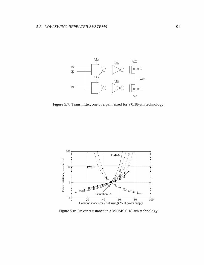
5.2. LOW-SWING REPEATER SYSTEMS 91
8.1/0.18
8.1/0.18Φ
Wire
Bit
Bit
1.8v1.8v
1.8v1.8v
0.5v
Figure 5.7: Transmitter, one of a pair, sized for a 0.18-µm technology
Saturation Ω
PMOS
NMOS
Common mode (center of swing), % of power supply
Dri
vere
sist
ance
,nor
mal
ized
100806040200
100
10
1
0.1
Figure 5.8: Driver resistance in a MOSIS 0.18-µm technology
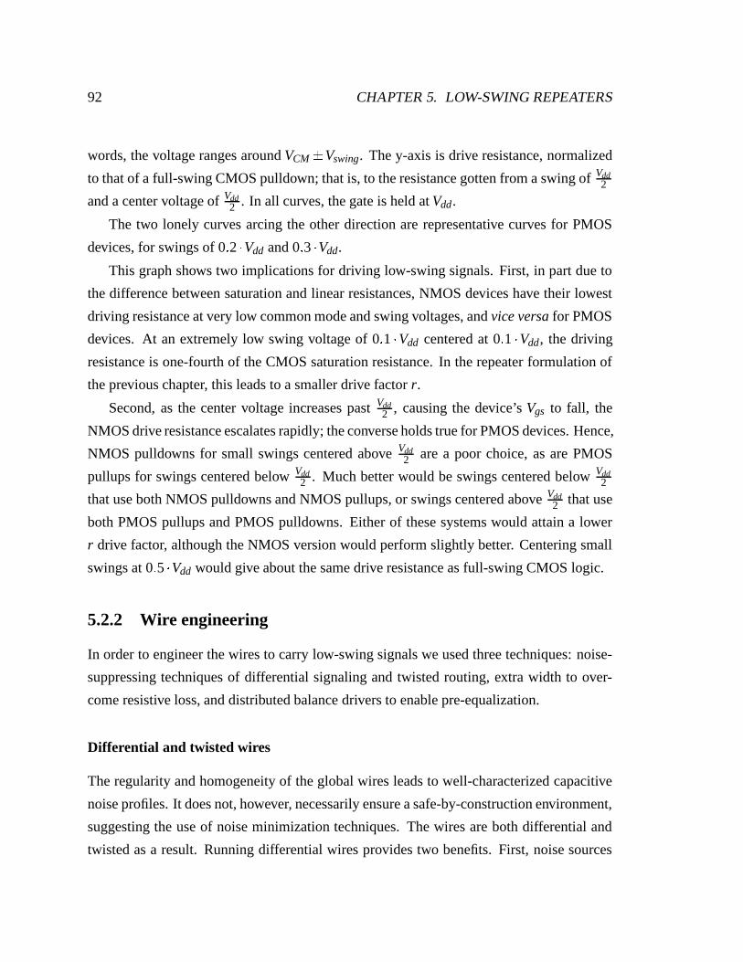
92 CHAPTER 5. LOW-SWING REPEATERS
words, the voltage ranges around VCM
Vswing. The y-axis is drive resistance, normalized
to that of a full-swing CMOS pulldown; that is, to the resistance gotten from a swing of Vdd2
and a center voltage of Vdd2 . In all curves, the gate is held at Vdd.
The two lonely curves arcing the other direction are representative curves for PMOS
devices, for swings of 0 2 Vdd and 0 3 Vdd.
This graph shows two implications for driving low-swing signals. First, in part due to
the difference between saturation and linear resistances, NMOS devices have their lowest
driving resistance at very low common mode and swing voltages, and vice versa for PMOS
devices. At an extremely low swing voltage of 0 1 Vdd centered at 0 1 Vdd, the driving
resistance is one-fourth of the CMOS saturation resistance. In the repeater formulation of
the previous chapter, this leads to a smaller drive factor r.
Second, as the center voltage increases past Vdd2 , causing the device’s Vgs to fall, the
NMOS drive resistance escalates rapidly; the converse holds true for PMOS devices. Hence,
NMOS pulldowns for small swings centered above Vdd2 are a poor choice, as are PMOS
pullups for swings centered below Vdd2 . Much better would be swings centered below Vdd
2
that use both NMOS pulldowns and NMOS pullups, or swings centered above Vdd2 that use
both PMOS pullups and PMOS pulldowns. Either of these systems would attain a lower
r drive factor, although the NMOS version would perform slightly better. Centering small
swings at 0 5 Vdd would give about the same drive resistance as full-swing CMOS logic.
5.2.2 Wire engineering
In order to engineer the wires to carry low-swing signals we used three techniques: noise-
suppressing techniques of differential signaling and twisted routing, extra width to over-
come resistive loss, and distributed balance drivers to enable pre-equalization.
Differential and twisted wires
The regularity and homogeneity of the global wires leads to well-characterized capacitive
noise profiles. It does not, however, necessarily ensure a safe-by-construction environment,
suggesting the use of noise minimization techniques. The wires are both differential and
twisted as a result. Running differential wires provides two benefits. First, noise sources
5.2. LOW-SWING REPEATER SYSTEMS 93
equally exposed to the two wires, such as a wide precharged bus running perpendicularly
over the wires, injects not differential but rather common-mode noise, which most receivers
can reject. Second, a wire whose complement sits next to it has a very close—and thus
low impedance—return path. The current loop for that wire becomes minimal, especially
as much of the current flow returns along the wire length as displacement current across
coupling capacitors, thereby minimizing inductive coupling.
Differential wires do cost twice as many wires for routing, but under technology scaling,
the number of total wire layers continues to increase slowly. As a result, the number of wire
pitches per gate increases, making the incremental cost of differential signaling smaller
with technology scaling.
A
A_bar
B
B_bar
C
C_bar
At least 2.5 pitches
Figure 5.9: A typical twist solution
Wire twisting at regular intervals down the bus eliminates differential noise injection
from neighboring wires and also helps to average out Miller capacitance to other bits,
thus minimizing data-dependent delays. Figure 5.9 shows a typical twisting pattern that
uses few metal resources from a neighboring metal layer. In this case, wire “B” couples
equally to both “A” and “A bar,” as well as equally from “C” and “C bar.” It suffers from
high total capacitance, because “B” and “B bar” are tightly coupled and always moving in
opposite direction. Other twisting schemes can reduce this worst-case Miller capacitance,
but typically consume more wires in a lower or upper layer for farther twists.
Using twisted wires demands some care. Each twist requires vias placed in-line with
the wire. Without using arrayed vias to reduce via resistance, the twists may add non-trivial
additional loss to the line.

94 CHAPTER 5. LOW-SWING REPEATERS
In this figure, the twists happen at regular and evenly-spaced intervals. However some-
times a better twisting arrangement can be used. Figure 5.10 shows this situation, where
capacitor C1 and capacitor C2 ideally push and pull equivalent current onto and off of the
victim.
Attacker
Victim
C1 C2
Figure 5.10: Optimized twisting would put the twist at 70% down the wire
The problem is that the noise contributions from C1 and C2 are not equal. Current from
C1 will split: most of it will drain harmlessly down the victim’s drive resistor at the left
of the line, and the rest will flow down to the far end, causing potential problems at the
victim’s receiver. Conversely, negative current from C2 will also split: some will go the
long route to the left, and most will go to the right, towards the victim’s receiver. Thus, for
a twist point at mid-way down the wire, the currents from C2 will overpower the currents
from C1, simply because C2 is closer to the victim’s receiver than C1 is. Moving the twist
point to the right may help, by reducing the proximity-aided influence of C2 on the victim’s
receiver. Too far, however, and the diminishing value of C2 will make C1 too important.
A first-order model of this assumes a constant attacker edge rate down the wire, so that
injected currents are proportional to C1 and C2. The current due to C1 must flow down the
victim wire to the receiver before it matters. This delay matches to first order the attacking
edge flowing down the attacker wire, so that C1’s current should reach the victim receiver
somewhat aligned with C2’s current. Hence we can simply consider the peak current levels
due to C1 and C2.
Injected currents see a resistor divider whose values are simply the left and right por-
tions of the victim wire. In this case, balancing the currents that flow to the right of the
victim wire, if the twist is at x (normalized between 0 and 1), requires:
C1
x2
C2
x
1 x2
(5.2)
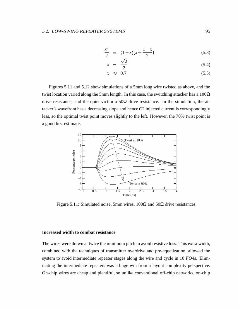
5.2. LOW-SWING REPEATER SYSTEMS 95
x2
2
1 x x 1 x
2 (5.3)
x 22
(5.4)
x 0 7 (5.5)
Figures 5.11 and 5.12 show simulations of a 5mm long wire twisted as above, and the
twist location varied along the 5mm length. In this case, the switching attacker has a 100Ωdrive resistance, and the quiet victim a 50Ω drive resistance. In the simulation, the at-
tacker’s wavefront has a decreasing slope and hence C2 injected current is correspondingly
less, so the optimal twist point moves slightly to the left. However, the 70% twist point is
a good first estimate.
Twist at 90%
Twist at 10%
Time (ns)
Per
cent
age
nois
e
43.532.521.510.50
12
10
8
6
4
2
0
-2
-4
-6
-8
Figure 5.11: Simulated noise, 5mm wires, 100Ω and 50Ω drive resistances
Increased width to combat resistance
The wires were drawn at twice the minimum pitch to avoid resistive loss. This extra width,
combined with the techniques of transmitter overdrive and pre-equalization, allowed the
system to avoid intermediate repeater stages along the wire and cycle in 10 FO4s. Elim-
inating the intermediate repeaters was a huge win from a layout complexity perspective.
On-chip wires are cheap and plentiful, so unlike conventional off-chip networks, on-chip
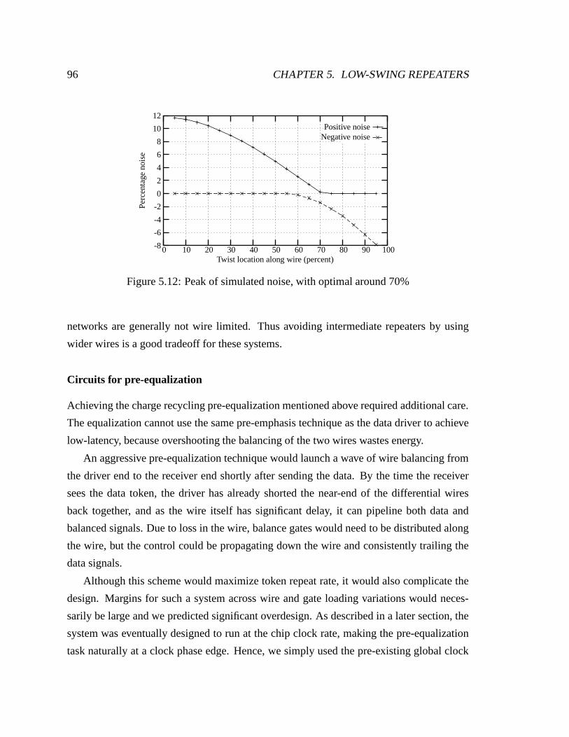
96 CHAPTER 5. LOW-SWING REPEATERS
Negative noisePositive noise
Twist location along wire (percent)
Per
cent
age
nois
e
1009080706050403020100
12
10
8
6
4
2
0
-2
-4
-6
-8
Figure 5.12: Peak of simulated noise, with optimal around 70%
networks are generally not wire limited. Thus avoiding intermediate repeaters by using
wider wires is a good tradeoff for these systems.
Circuits for pre-equalization
Achieving the charge recycling pre-equalization mentioned above required additional care.
The equalization cannot use the same pre-emphasis technique as the data driver to achieve
low-latency, because overshooting the balancing of the two wires wastes energy.
An aggressive pre-equalization technique would launch a wave of wire balancing from
the driver end to the receiver end shortly after sending the data. By the time the receiver
sees the data token, the driver has already shorted the near-end of the differential wires
back together, and as the wire itself has significant delay, it can pipeline both data and
balanced signals. Due to loss in the wire, balance gates would need to be distributed along
the wire, but the control could be propagating down the wire and consistently trailing the
data signals.
Although this scheme would maximize token repeat rate, it would also complicate the
design. Margins for such a system across wire and gate loading variations would neces-
sarily be large and we predicted significant overdesign. As described in a later section, the
system was eventually designed to run at the chip clock rate, making the pre-equalization
task naturally at a clock phase edge. Hence, we simply used the pre-existing global clock
5.2. LOW-SWING REPEATER SYSTEMS 97
signal to control multiple equalization circuits distributed along the wire. These distributed
balance devices presented an additional load to the clock.
In our design for a 10mm wire we used five evenly-spaced 3.6 µm-wide balance devices,
at 0, 25%, 50%, 75%, and 100% down the line. This many devices allowed smaller sizes,
but even so, the balance devices had a total gate width double that of the driver. Fewer
balance devices would have been correspondingly larger: SPICE simulations confirmed
that three equalizers would have been 30-µm wide each; two equalizers would have been
140-µm wide each; and a single equalizer could not have worked, even at sizes exceeding
250-µm. These relationships arise from a cubed relationship between balance driver sizes
and the distance between drivers: as the distance between balance drivers grows by x, the
difference between our 4FO4s time limit and the wire RC shrinks by x2. In addition, the
balance driver must drive a portion of the wire C in this shrinking time, and that wire
capacitance has also grown by x. These two terms combine for an x3 dependency between
the balance device spacing and the balance device sizes.
In a real design we would also provide small—1.2 µm in the testchip—passgates to a
shunt supply at the balance voltage, to fix DC drifts from imperfect balancing.
5.2.3 Low-swing receivers
A simple regenerative sense amplifier, drawn in Figure 5.13, followed by an optimized R/S
latch [92] performs full logic amplification of low-swing inputs. This section will discuss
three design considerations for this particular circuit: common-mode and swing level of
the input voltage, offset voltage and mismatch, and clocking.
Amplifier delay and common-mode voltage
In Section 5.2.1 above, we discussed the use of NMOS devices at low common-mode
voltages, and their drive resistance advantage over PMOS drivers at high common-mode
voltages. This should motivate us to use PMOS input gates in the regenerative amplifier
to properly receive low input voltages. As it turns out, the amplifier would also prefer low
common-mode input voltages.
Considering only the sense-amplifier itself, and not the R/S latch, which has a fixed

98 CHAPTER 5. LOW-SWING REPEATERS
voa a o
v
Vdd
Bit
Φ
Φ
Φ Φ
Φ
2.88/0.24
S/R latch
Bit
Figure 5.13: Receiver amplifier, in 0.18-µm technology
delay, we can model the amplifier latency in two parts. First, the clock trips and the two
input gates pull current up each side of the amplifier. These devices are saturated, and so
their currents are constant. These currents charge up the inverters from their pre-discharged
states. After some time, the amplifier’s cross-coupled inverters kick into a regenerative
feedback loop and the amplifier switches; during this stage, the input devices play only a
very minor role in the amplifier’s operation.
A highly simplified model of this amplifier can help illustrate its delay. This model
assumes that the devices are velocity saturated; while PMOS gates in today’s technologies
are not completely velocity saturated, they are close, and this assumption dramatically
simplifies the model. In this case, we can write the input voltages as V1 Vcm
∆V and
V2 Vcm ∆V , and the corresponding currents as:
I1 Kp
Vcm
∆V Vt Icm ∆I (5.6)
I2 Kp
Vcm ∆V Vt Icm ∆I (5.7)
Icm Kp
Vcm Vt (5.8)

5.2. LOW-SWING REPEATER SYSTEMS 99
∆I Kp∆V (5.9)
The time required for the first stage, as the constant currents pull up either side of the
cross-coupled amplifiers, can be written as
t1
CtotVswing
Icm
CtotVt
Icm
Ctot14Vdd
Icm(5.10)
where the current is the common-mode current; the capacitance is the total load capaci-
tance; and the voltage swing is a threshold drop Vt . This last term arises because once the
output nodes exceed Vt , the inverters begin to regenerate, driving one of the input transis-
tors out of saturation (the input devices stay saturated for a while, governing the current
through the cross-coupled inverters, so this is only an approximation). Here we assume
that the threshold voltage is roughly one-fourth the power supply.
The time required for the second regeneration stage depends logarithmically on the volt-
age gain, where the regeneration time constant is a lightly-loaded inverter delay (0.35FO4s).
The voltage gain depends on how far the nodes have split when the regeneration kicks in,
and this can be written as
t2 0 35logVdd
Vstart(5.11)
Vstart
1Ctot
t1
02∆Idt
2Kp∆V
Ctott1 (5.12)
We can consider two cases. In the first case, the input voltages are centered about
0 5Vdd, so that the common-mode voltage is simply 0 5Vdd. Assuming that a threshold
voltage is one-fourth the power supply leads to an expression
DfixedCM
2Ctot
Kp
0 35log
1swing
(5.13)
In a full-swing case, when the second term is zero, the first term (an RC product) looks like
the delay of a three-input NOR, since the circuit has three series PMOS gates. This “NOR”
drives a load whose size makes it look like it has a fanout of 2.25. This results in a delay of

100 CHAPTER 5. LOW-SWING REPEATERS
about 1.3FO4s.
DfixedCM 1 3
0 35log1
swing(5.14)
In the second case, the common-mode voltage falls along with the swing, increasing
the constant current. In this case, the higher common-mode current pulls up the inverter
nodes faster—shorter t1–but also gives the differential current ∆I less time to split apart the
regenerative nodes—longer t2. Here, taking Vcm Vdd ∆V , so that the common-mode
falls with the swing, and again assuming that Vt Vdd
4 leads to an expression
DvariableCM
1 33 2x
0 35log
3 2xswing
(5.15)
Figure 5.14 compares this simple model to simulation, and shows that the amplifier
indeeds operates quickest for low common-mode inputs and small swings. Because the
amplifier regeneration speed easily outstrips a wire time constant, a strategy for low latency
would be to transmit very low swings and let the amp, not the wire drivers, do all the work.
However, as seen in the next section, swings that are too small run the risk of failure.
Variable CM (model)Variable CM (simulation)
Fixed CM (model)Fixed CM (simulation)
Swing, fraction of supply
Del
ay,F
O4s
10.90.80.70.60.50.40.30.20.10
3
2.8
2.6
2.4
2.2
2
1.8
1.6
1.4
1.2
1
Figure 5.14: Sense amplifier delays
5.2. LOW-SWING REPEATER SYSTEMS 101
Mismatch and offsets
The problem with swings that are too small is that they might not overcome inherent,
systematic inaccuracies in the receiver [93][94]. If the receiver has a bias to evaluate one
way over the other, then any inputs whose difference does not overcome that bias will cause
the amplifier to give the wrong answer.
This intrinsic offset in the amplifier is dominated by geometric and Vt mismatches in
the two PMOS input devices, as well as by geometric and Vt mismatches in the inverter’s
PMOS devices; the inverter’s PMOS devices are important because any mismatch on their
source voltage maps directly to their gate overdrive. The NMOS devices have a corre-
spondingly smaller effect on mismatch.
As the common-mode input falls and the current increases, the offset voltage worsens.
We can see this by considering just the input pair mismatches in Vt and β. Suppose β1 β2
but we still want i2 i1 when input voltage V2
V1. In this case, we can define
β β1
β2
2(5.16)
∆β β1 β2
2(5.17)
(5.18)
If we define v1 Vgs Vt1 Vtail and v2 similarly, then when the input voltage V2 exceeds
input voltage V1, correct behavior of the pair occurs if
i2 i1 (5.19)
β ∆β vα
2
β ∆β vα1 (5.20)
βvα
2 vα1 ∆β
vα
2
vα1 (5.21)
vα1 vα
2
vα1
vα
2
∆ββ
(5.22)
The right side of the last equation is fixed. So as the denominator term on the left side
(the total current in the amp) rises with decreasing common-mode voltage, the numerator
term (the differential input voltage) must also rise to compensate. Hence the offset increases
with decreased common-mode voltage.
102 CHAPTER 5. LOW-SWING REPEATERS
The receivers were sized to balance input offset voltage and clocking power. For input
devices sized W/L=2.88/0.24µm in an 0.18-µm technology, SPICE simulations predicted
3σ offsets of 86mV. However, we added margin to this offset estimate because it was based
on projections and extrapolations from other technologies. Therefore the system assumed
offsets of 100mV.
In hindsight, we know that power in the drivers and equalization devices dominate that
in the receiver’s amplifier, so using larger amplifiers with correspondingly lower offsets
would have been a better choice. Table 5.1 shows these estimated tradeoffs as the receiver’s
device widths vary from normal to 2.4x normal. In this table, amplifier offsets fall by the
square-root of the width increase. Adding 15% margin to these offsets for a “minimum
safe swing” enables calculations of energy savings, because SPICE simulations show that
the wire energy of the baseline system is 18% of the total system energy. Also, the increase
in energy cost from the larger amplifier comes from simulations showing that the amplifier
accounts for 8% of the total system energy. We see that a receiver about 1.6x the size
actually used would have been preferable, although the benefit is fairly small. A further
Receiver Receiver Safe Benefit in Cost inSize Offsets Swing Power (from wires) Power (from rcvr)
100% 86mV 100mV 0% 0%120% 78mV 90mV 3.42% -1.6%140% 73mV 84mV 5.22% -3.2%160% 68mV 78mV 7.02% -4.8%180% 64mV 74mV 7.92% -6.4%200% 61mV 71mV 9.00% -8.0%220% 58mV 67mV 9.90% -9.6%240% 56mV 64mV 10.8% -11.2%
Table 5.1: Estimated improvements to receiver sizing
improvement to the receiver circuits would use well-known offset compensation schemes
to reduce the offsets further.

5.2. LOW-SWING REPEATER SYSTEMS 103
Clocking
Receivers circuits need to be clocked for power efficiency reasons. Not doing so would
otherwise leave the amplifiers in a continually high-gain, high-power state and with little
room for power optimization [95]. Clocking the receivers can be done in one of two ways.
First, the sender can package a clock signal to indicate that the receivers should strobe
the data. Sending a clock with the data complicates the design: the clock must be full-
swing, or else the receiver does not know when to sample and amplify the clock. But as
a full-swing signal, the clock signal will have a different delay from the low-swing data
lines, and so matching these delays requires careful circuit design: timing the clock too late
wastes power, and timing the clock too early may return incorrect data if some of the data
wires have not yet overcome their receivers’ offsets.
A related question involves “kiting”: the full-swing clock consumes enough energy
that it should be bundled with a large number of receivers, to amortize its energy cost. But
buffering up the clock to drive a wide bank of receivers takes time and hence requires the
clock to be launched earlier than the data, or “kited”1. Getting the kite delay exactly right
might add more design complexity. Suppose the low-swing data is an order of magnitude
more efficient than the full-swing clock. To keep the clock power overhead minimal, to
under 10% of the total power cost, we would bundle on order of 100 data lines per clock
line. In an 0.18-µm technology, optimally repeating the clock wire would result in a final
gate driver of around 20µm of gate. Assuming the receivers each present a clock load of
around 6µm, this results in a required step-up of 30, or 2-3 FO4s of “kiting.”
Second, a much-simplified clocking scheme uses the global chip clock as our clocking
source. Leveraging this existing, low-skew, globally-distributed clock is a cheat, because
it makes the job of the clock distribution network marginally more complicated. However,
it also dramatically simplifies the design, and for this reason the final design and testchip
used such a global clocking scheme.
By clocking the receivers with a global clock, we by necessity peg the transfer latency
to a clock phase. This changes the figure of merit for the interconnect system, from ps/mm
units into “distance travelled in a clock phase.” Also, clock-gating now requires a more
1Following Sutherland’s asynchronous parlance, we need to kite the clock, or “float” it ahead of the data[96].

104 CHAPTER 5. LOW-SWING REPEATERS
sophisticated scheme, in which a suppress signal sent in a cycle means that the next cycle’s
data should not be read.
5.3 Putting it all together
To explore this design space, we built simulations of the low-swing signalling system and
compared its behavior and performance to that of a full-swing CMOS system. Using a
commodity TSMC/MOSIS 0.18-µm technology we designed the drivers and receivers to
communicate over 10mm of length at a 10FO4 repeat rate. This closely matched the pro-
jected wire characteristics of the Smart Memories target vehicle.
After optimizing both sizing and the driver power supply, the bus needed 0.8pJ/bit, or
just about an order of magnitude less energy than the CMOS full-swing bus. This energy
cost included all of the clocking overhead. In this system, the drivers used drive voltages
of 0 and 0.5V, with pre-equalization to 0.25V, and a developed difference of 90mV by
the time the sense-amp fired. Simulations showed that 55% of the energy was consumed
in the driver and balance devices, 25% in the sense-amp, and the remaining 20% in the
wires themselves. Compared to the full-swing system, this system hit the same timing
deadlines—one link per clock phase—but for up to an order of magnitude less power. With
lower activity factors, the energy improvement decreases, unless clock-gating implemented
via supression signals is used.
These results motivated further study into low-swing interconnect. Simulations can be
revealing, but they rarely reveal all of the problems in a design, and so we assembled some
testchips containing low-swing wire systems. In the next chapter we will discuss the results
of those experiments.

Chapter 6
Experimental Results
The last chapter reviewed design considerations for a low-swing interconnect system, and
described how a simulation of such a system demonstrated communication over a 10mm
on-chip bus with a 10 FO4 latency and with up to ten times less energy than standard
CMOS repeaters.
While this looked great, simulations often look great. They cannot answer several
key questions: Does the system actually work? What are the real sense-amplifier offsets?
Did we miss any energy consumers in our calculation of power savings? Therefore we
built a testchip to attempt to answer these and more questions. We found that the system
communicated without errors over the target bus at the target rate, and that it in fact saved
an order of magnitude in power over a full-activity full-swing bus; with lower activity
factors on the full-swing bus, the energy improvement decreases. We also measured offsets
on a 0.25-µm technology and found our design to have 3 5σ offsets under 80mV, with
residual uncertainties after offset cancellation to be around 15mV at 3σ.
6.1 Testchip overview
We used a MOSIS 0.18-µm technology, fabricated by TSMC, with six layers of aluminum
interconnect. The testchip emerged on a fabrication run significantly faster than previous
runs through MOSIS, according to the parametric SPICE models on the MOSIS website.
The chip had measured FO4 delays of 95ps at a voltage of 1.8V and room temperature, a
105
106 CHAPTER 6. EXPERIMENTAL RESULTS
20% speedup over the previous fabrication runs. The testchip had an area of 9.2mm2 and
was edge wirebonded inside an 84-pin Kyocera ceramic package.
The testchip contained four major experiments. First, we designed a number of low-
swing buses of varying lengths and bus construction. We used 5mm, 7mm, and 10mm
buses, and in each length we built a single-bit bus, a two-bit bus, and a three-bit bus, in
order to see coupling effects. These buses used twisted wires for differential noise rejection,
but we also duplicated the 10mm bus once without any wire twisting to see the effects of
the twists. Because the die itself had edge lengths of only 3mm, the buses needed to be
serpentined back along themselves to reach their full length. This also allowed the drivers
to be physically close to the receivers.
These low-swing buses had isolated power supplies to enable accurate energy measure-
ments. We also attached comparators between the drivers and the nearby receivers, so that
we could compare what had been sent with what had been received. These error-checkers
would power up a board LED if they detected a mismatch, although they could not identify
which bit or clock generated the error.
Second, we constructed full-swing buses, sized and repeated for a minimum energy-
delay product, to send signals at a 10 FO4 latency. These buses, using standard CMOS
inverters as repeating elements, spanned 5mm and 10mm lengths and used the same error-
catching circuits as the low-swing buses. They enabled a fair apples-to-apples power com-
parison between low-swing and full-swing interconnect schemes.
Third, to explore the offsets present in our sense-amplifiers, we constructed a large
array of them, all commonly-clocked and all able to shift out their outputs in a chain. By
varying the input voltages we could use this to gather statistics on amplifier mismatch.
Unfortunately, we mis-designed the scan chain, breaking it logically, and so we had to re-
spin just this particular block onto another vendor’s 0.25-µm technology in order to see any
results. To first order, the Vt mismatch between two devices does not change if we scale
their widths and lengths: the effect of decreased area is countered by the effect of scaled
gate oxides. Therefore results from the 0.25-µm chip are still interesting.
Fourth, we included a self-contained block of oscillators in order to test the native speed
of the chip. This block had its own pads and could be wire-bonded separately on a few parts
per lot in order to save pads for the rest of the chip.
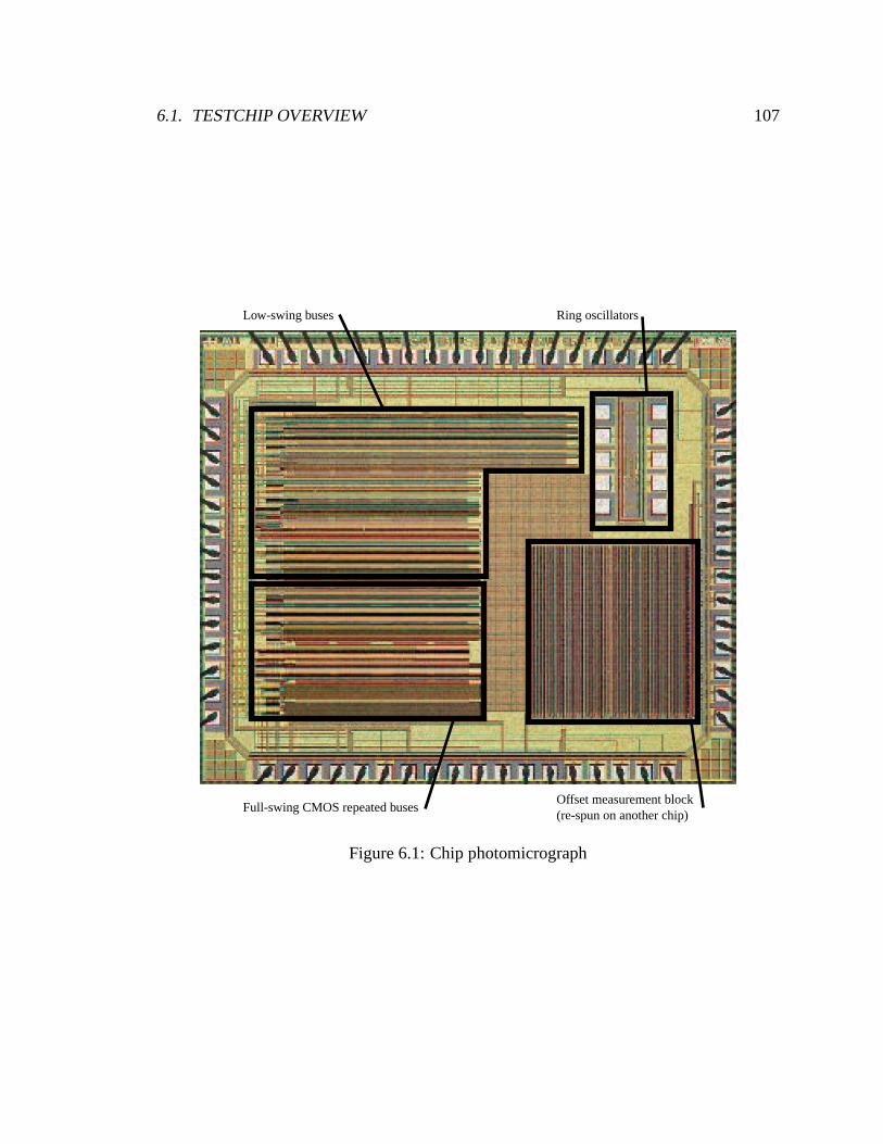
6.1. TESTCHIP OVERVIEW 107
Low-swing buses Ring oscillators
Offset measurement block (re-spun on another chip)
Full-swing CMOS repeated buses
Figure 6.1: Chip photomicrograph

108 CHAPTER 6. EXPERIMENTAL RESULTS
Figure 6.1 shows a die photomicrograph of the chip, with the four major blocks outlined
in black.
6.2 Bus experiments
The low-swing buses followed the guidelines listed in the previous chapter. A four-way
ping-pong device connected to each bus driver’s input, in which four scan-loadable flip/flops
alternately fed the driver on four successive clocks. This way, any four-bit pattern, includ-
ing the “quiet-low” pattern of 0000 and the “quiet-high” pattern of 1111, could be transmit-
ted down the wire. The drivers used NMOS linear-mode drivers, with low common-mode
voltages, overdrive pre-emphasis and pre-equalization between data tokens. For the over-
drive, the buses aimed for a common-mode equalization voltage of 0.25V with drive power
supplies of 0 and 0.5V.
The wires ran as a differential pair, twisted along the route to reject outside noise. An
extra version of the 10mm bus, without any twisting but identical otherwise, provided a
measure of the twisting effectiveness. Balance devices sat every 25% down the wires to
achieve fast pre-equalization, along with trickle devices connecting the wires to a Vbalance
supply to correct mismatched pre-equalization gates.
A receiver, clocked off of the chip clock, amplified a new token each phase, presum-
ably after the development of 90mV of signal. The receiver fed the outputs into an error-
checking comparator that had stored the driver’s sent data from the previous clock phase.
On any mismatch a pin was driven high to light an LED on the board.
To make the chip more realistic, a number of large inverters placed below the buses
could be clocked to inject noise into the system. These inverters were turned off during
power measurements, because they used the same supply as the buses, and they do not
show up in the figures below, although they were active during exploration of the voltage
and speed margins.
For test and measurement, many on-chip voltage sampling oscilloscopes captured wave-
forms for validation of performance, and they provided the figures in this chapter. Their
design will be discussed briefly below.
The reliability of the link was not well instrumented, making unavailable traditional

6.2. BUS EXPERIMENTS 109
reliability metrics like pseudo-random data bit error-rate. Claims that the low-swing bus
“worked” meant running the chip for several hours and not seeing any errors; in one case
the chip ran over a weekend with no errors. However, the bit patterns available for test were
only simple repeating four-bit patterns and not more sophisticated PRBS generators.
As the design of the low-swing buses targeted tranmission of a new token across the
10mm link every 10 FO4s, the full-swing CMOS repeated buses next to them were de-
signed to hit the same 10 FO4 latency for the same length hop. This would provide the
fairest energy comparison. In addition, because the low-swing buses used two non-minimal
wires per bit, the full-swing buses were given equivalent wire resources and thus had nice,
fat, widely-spaced wires. This was again to ensure a fair energy comparison.
6.2.1 Overhead
Because full-swing CMOS repeaters do not need a clock, they have no need to cross the
entire hop in the 10 FO4s: unlike the low-swing repeaters, the penalty for placing a re-
peater between the hop end-points costs only area and via congestion and does not require
generating any special phase-dividing timing signals.
As a result, the full-swing CMOS buses used repeaters placed for optimal energy given
a 10 FO4 latency target, and therefore broke the 10mm wire into three equal sections. In
simulation we found that if repeated for optimal latency, they would have reached across
the 10mm hop in just over 7.5 FO4s, so that they had a native 25% speed improvement
over our low-swing buses. However, on the chip they were throttled-back somewhat to hit
10 FO4s.
The active devices in the low-swing experiment consumed nearly 75% more area than
the active devices in the full-swing CMOS buses. The additional area went to the complex
receivers, pre-equalization clamps, and drivers. However, the total area of the bus is com-
pletely dominated by the wires and not by the active devices, so the overall area penalty is
less than 12 %.
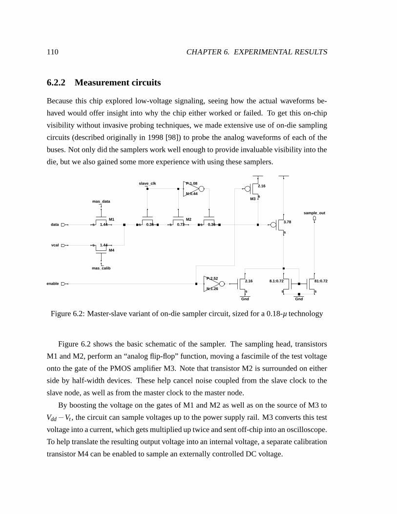
110 CHAPTER 6. EXPERIMENTAL RESULTS
6.2.2 Measurement circuits
Because this chip explored low-voltage signaling, seeing how the actual waveforms be-
haved would offer insight into why the chip either worked or failed. To get this on-chip
visibility without invasive probing techniques, we made extensive use of on-die sampling
circuits (described originally in 1998 [98]) to probe the analog waveforms of each of the
buses. Not only did the samplers work well enough to provide invaluable visibility into the
die, but we also gained some more experience with using these samplers.
data
vcal
slave_clk
mas_data
mas_calib
enable
1.44s
0.36s 0.72s 0.36s
P:1.08
N:0.44
2.16
s
3.78
s
P:2.52
N:1.26
2.16
s
Gnd
81:0.72
s
Gnd
8.1:0.72
s
sample_out
1.44sM1 M2
M3
M4
Figure 6.2: Master-slave variant of on-die sampler circuit, sized for a 0.18-µ technology
Figure 6.2 shows the basic schematic of the sampler. The sampling head, transistors
M1 and M2, perform an “analog flip-flop” function, moving a fascimile of the test voltage
onto the gate of the PMOS amplifier M3. Note that transistor M2 is surrounded on either
side by half-width devices. These help cancel noise coupled from the slave clock to the
slave node, as well as from the master clock to the master node.
By boosting the voltage on the gates of M1 and M2 as well as on the source of M3 to
Vdd
Vt , the circuit can sample voltages up to the power supply rail. M3 converts this test
voltage into a current, which gets multiplied up twice and sent off-chip into an oscilloscope.
To help translate the resulting output voltage into an internal voltage, a separate calibration
transistor M4 can be enabled to sample an externally controlled DC voltage.

6.2. BUS EXPERIMENTS 111
The sampler can be run in one of two modes. In one mode, the sampler clock and the
chip clock have the same frequency, and the chip is placed in a repetitive pattern. Over
many cycles of operation, the sampler continually samples the same voltage, ensuring that
the gate of M3 gets charged to the full voltage on the node under test. We can record the
resulting output voltage and translate it to an on-chip voltage. Then, by stepping the phase
relationship between the two (identical frequency) clocks, we can map out another voltage.
By repeating this process, we can eventually draw a very accurate waveform.
In the other mode, we set the sampler clock and the chip clock to have very slightly
different frequencies. Now, each cycle the sampler examines a slightly different point on
the test waveform, and by dialing out the time base of the oscilloscope to the beat frequency
of the two clocks, we will get a (slightly inaccurate) picture of the real on-chip waveform
on the oscilloscope. In this mode, charge-sharing across gate M2 limits the bandwidth of
the sampler, although changing the beat frequency can control this bandwidth limit. Jitter
in the sampler clock, on the other hand, blurs the sampled signal over the jitter interval,
making it a more serious bandwidth limiter.
In this testchip, not every wire was sampled, but those that were had two samplers each:
one on the true wire and on one the complement. The true wire used a sampler very similar
to those as used on previous chips (see Figure 6.2), while the sampler on the complement
wire inserted a simple buffer-amplifier in-between the NMOS input passgates in an attempt
to eliminate the pole that arises from charge-sharing across the slave NMOS passgate. In
every case, however, the waveforms from the two samplers did not noticeably differ when
we overlaid them (by using one sampler with one data set, and then the other sampler with
the complement data set). This indicated that the charge-sharing pole was unimportant.
The difference in loading on the true and complement wires from the two different types of
samplers, or simply between an inactive and an active sampler, was negligible.
A more robust sampling circuit would have used a differential read path on both of
the true and complement wires. However, the testchip used separately-sampled differential
wires with two different types of single-ended samplers. This was primarily to reduce the
likelihood of design errors in the samplers preventing any measurements.
By using an extra sampler to sample the chip clock, we gained a timing reference. Sam-
pling the chip clock returns a clock at the beat frequency between the chip and sampling

112 CHAPTER 6. EXPERIMENTAL RESULTS
clock, and we can use this beat clock as the trigger for the oscilloscope. This aligns all
sampled data in time, allowing us to line up graphs properly and calculate delays.
Per-sampler calibration was extremely important. The calibration curves, though con-
stant for each sampler, varied significantly between sampler sites. Especially for measur-
ing voltages that hover near 0V, eliminating uncertainty from uncalibrated devices became
paramount.
Finally, we made a nearly unrecoverable error in the sampler design. The final output
node, carrying the magnified current from the two series current mirrors, routed to a chip
pin over a long and winding route. This meant that signficant current out of the sampler
would cause significant iR drop along that wire, thereby pushing the current mirror out
of saturation. This clamped the output current, effectively making the sampler much less
responsive to any change in sampled voltage, if the voltage were low enough. As the nodes
in question were small-swing at low voltages, this was very nearly fatal.
The fix was to not ground the current mirror output at ground with the oscilloscope
input, but rather to drive it down to -2V through a discrete 50Ω resistor. This way, the iR
drop along the output wire would still give the current mirror sufficient headroom to stay
saturated and maintain sensitivity to the sampler.
6.2.3 Performance and results
The low-swing buses performed at 10 FO4 per cycle, or just about 1GHz, but required a
higher driving voltage than predicted. Instead of the planned 0.5V drive voltage, the system
required just over 0.6V of drive voltage, and a pre-equalization voltage of 0.3V. In other
words, the error LED on the board did not remain off until the drive voltage reached 0.6V.
Upon exploration of the layout, we found that our clock spine, distributing the clock to
the various drivers and receivers, was thin, scenically-routed, and replete with clock skew.
Although we did not perform FIB experiments to adjust the clock routing, we speculate
that this contributed significantly to the bus failures below 0.6V of drive voltage. Unfortu-
nately, we were unable to observe any clock skew because we had no samplers sampling
chip clocks near the actual receivers, nor any samplers looking at signals derived from the
receiver clock.

6.2. BUS EXPERIMENTS 113
Measurement pictures
Figures 6.3 and 6.4 show sampled oscilloscope measurements taken from the 10mm low-
swing bus with three bits on the bus. The middle bit is plotted and the two outer bits are
quiet.
Figure 6.3 shows the system running at 500MHz. The outer curves show the waveform
at the driver end of the wire, and the inner curves show the waveform at the receiver end of
the wire. At 500MHz, or about 20 FO4s per token, the system has plenty of time to drive
the value down the wire, and the far end of the wire achieves nearly the full voltage split.
Due to very generous timing margins, the system worked fine down to a drive voltage of
0.4V and a pre-equalized balance voltage at 0.2V. At 0.5ns and 1.5ns the wires take sudden
jumps down and up in common-mode voltage; this is due to the clock signal coupling into
the data lines. Although the coupling may seem dramatic, the movement is only around
100mV, which is small compared to the 1.8V swing on the clock wires themselves.
Far EndNear End
Time (ns)
Vol
ts
21.510.50
1
0.8
0.6
0.4
0.2
0
Figure 6.3: Low-swing bus at 500MHz
Figure 6.4 shows the same bus running now at 1GHz. Again, the outer curves show
the driver end of the wire and the inner curves the receiver end of the wire. Because the
system speed is much faster, the receiver end of the wire barely splits past 90mV before
the clock phase ends and the wire begins to pre-equalize. By contrast, the driver-end of the
wire opens up to a wider voltage. As mentioned above, this system required a drive voltage
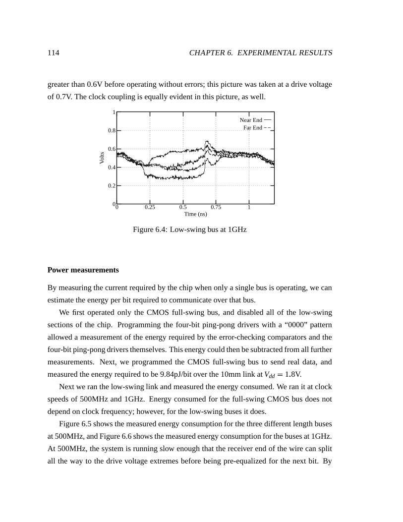
114 CHAPTER 6. EXPERIMENTAL RESULTS
greater than 0.6V before operating without errors; this picture was taken at a drive voltage
of 0.7V. The clock coupling is equally evident in this picture, as well.
Far EndNear End
Time (ns)
Vol
ts
10.750.50.250
1
0.8
0.6
0.4
0.2
0
Figure 6.4: Low-swing bus at 1GHz
Power measurements
By measuring the current required by the chip when only a single bus is operating, we can
estimate the energy per bit required to communicate over that bus.
We first operated only the CMOS full-swing bus, and disabled all of the low-swing
sections of the chip. Programming the four-bit ping-pong drivers with a “0000” pattern
allowed a measurement of the energy required by the error-checking comparators and the
four-bit ping-pong drivers themselves. This energy could then be subtracted from all further
measurements. Next, we programmed the CMOS full-swing bus to send real data, and
measured the energy required to be 9.84pJ/bit over the 10mm link at Vdd 1 8V.
Next we ran the low-swing link and measured the energy consumed. We ran it at clock
speeds of 500MHz and 1GHz. Energy consumed for the full-swing CMOS bus does not
depend on clock frequency; however, for the low-swing buses it does.
Figure 6.5 shows the measured energy consumption for the three different length buses
at 500MHz, and Figure 6.6 shows the measured energy consumption for the buses at 1GHz.
At 500MHz, the system is running slow enough that the receiver end of the wire can split
all the way to the drive voltage extremes before being pre-equalized for the next bit. By
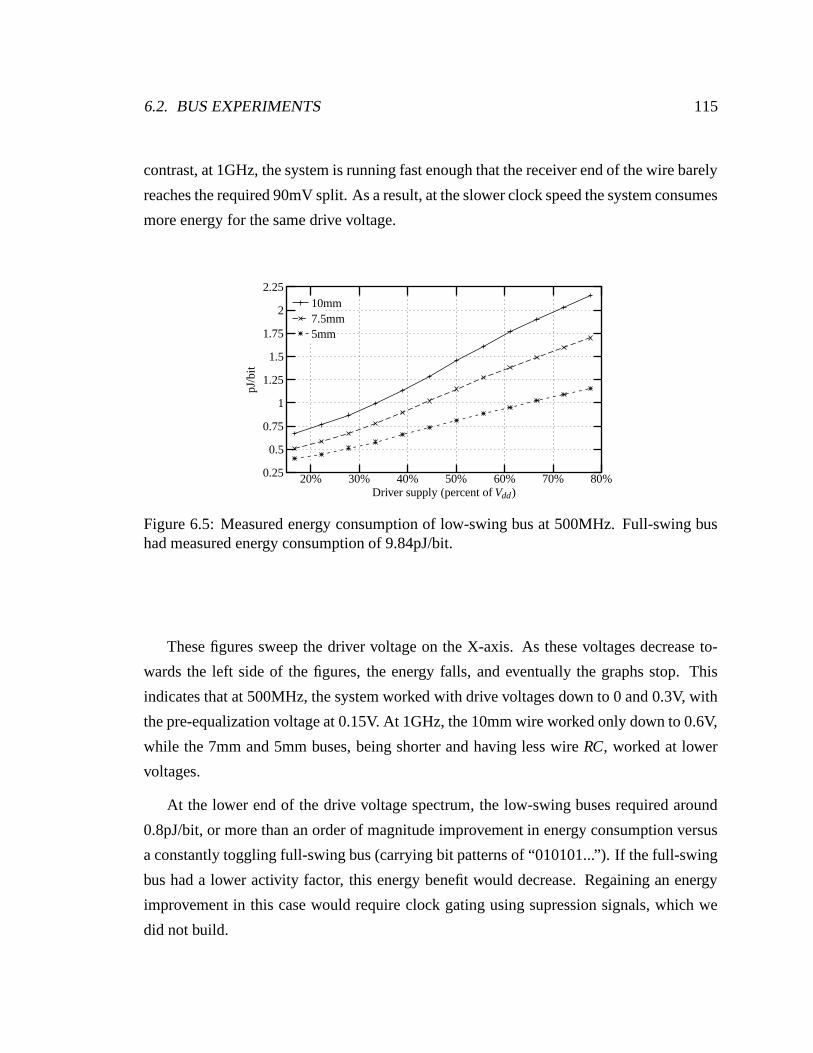
6.2. BUS EXPERIMENTS 115
contrast, at 1GHz, the system is running fast enough that the receiver end of the wire barely
reaches the required 90mV split. As a result, at the slower clock speed the system consumes
more energy for the same drive voltage.
5mm7.5mm10mm
Driver supply (percent of Vdd)
pJ/b
it
80%70%60%50%40%30%20%
2.25
2
1.75
1.5
1.25
1
0.75
0.5
0.25
Figure 6.5: Measured energy consumption of low-swing bus at 500MHz. Full-swing bushad measured energy consumption of 9.84pJ/bit.
These figures sweep the driver voltage on the X-axis. As these voltages decrease to-
wards the left side of the figures, the energy falls, and eventually the graphs stop. This
indicates that at 500MHz, the system worked with drive voltages down to 0 and 0.3V, with
the pre-equalization voltage at 0.15V. At 1GHz, the 10mm wire worked only down to 0.6V,
while the 7mm and 5mm buses, being shorter and having less wire RC, worked at lower
voltages.
At the lower end of the drive voltage spectrum, the low-swing buses required around
0.8pJ/bit, or more than an order of magnitude improvement in energy consumption versus
a constantly toggling full-swing bus (carrying bit patterns of “010101...”). If the full-swing
bus had a lower activity factor, this energy benefit would decrease. Regaining an energy
improvement in this case would require clock gating using supression signals, which we
did not build.

116 CHAPTER 6. EXPERIMENTAL RESULTS
5mm7.5mm10mm
Driver supply (percent of Vdd)
pJ/b
it
80%70%60%50%40%30%20%
2.25
2
1.75
1.5
1.25
1
0.75
0.5
0.25
Figure 6.6: Measured energy consumption of low-swing bus at 1GHz. Full-swing bus hadmeasured energy consumption of 9.84pJ/bit.
Efficacy of wire twisting
The 10mm bus was twisted along its length four times to reject outside noise. If we label
the wires in the three-bit bus A,B, and C, we have the six wires A,A,B,B,C, and C in a row.
Without any twisting, the above wire sequence remains the same all the way down the
wire. In this case, if we send a “1” down all three wires, then A will fall as B rises, and
C will rise as B will fall. This pattern generates the worst-case “hurt” coupling, because A
and C will restrict the opening of B’s data eye. Conversely, if we send a “0” down B as we
send “1”s down A and C, we get the best-case “help” coupling, as A and C aid in opening
B’s data eye.
With all wires twisted, all these effects should be nullified, at least to first order. Because
we also built a 10mm bus without any twists, we were able to view the actual effects of
such a twist. Figure 6.7 and 6.8 show the probed waveforms at the receiver side only. In
this experiment the buses ran at 1GHz. In Figure 6.7, the two waveforms are difficult to
distinguish; there is no difference between the “help” or “hurt” data patterns.
By contrast, the untwisted wires show that the hurt pattern has a worse data eye than
the help pattern. Interestingly, the untwisted wires, even with the hurt pattern, has a data
eye very close to that of the twisted wires. After some investigation we realized this re-
sulted from sloppy twists. Because the process uses aluminum interconnect, vias consist of
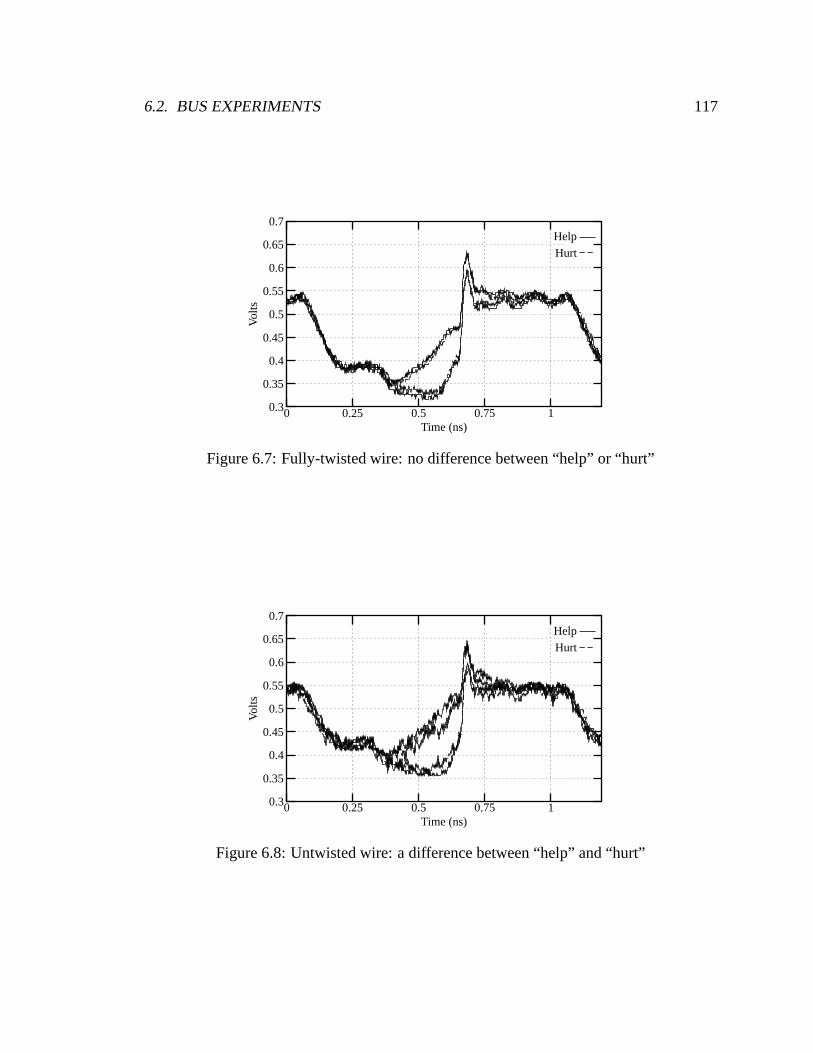
6.2. BUS EXPERIMENTS 117
HurtHelp
Time (ns)
Vol
ts
10.750.50.250
0.7
0.65
0.6
0.55
0.5
0.45
0.4
0.35
0.3
Figure 6.7: Fully-twisted wire: no difference between “help” or “hurt”
HurtHelp
Time (ns)
Vol
ts
10.750.50.250
0.7
0.65
0.6
0.55
0.5
0.45
0.4
0.35
0.3
Figure 6.8: Untwisted wire: a difference between “help” and “hurt”

118 CHAPTER 6. EXPERIMENTAL RESULTS
highly-resistive tungsten. The twists in the bus used only single vias and not wide arrays of
them, so that the twisted wires, although good at rejecting coupled noise, also had an extra
40Ω of resistance, assuming via resistance of 10Ω each. This led to a non-trivial increase
in total resistivity and implied that the twisting seemed effective, if poorly implemented.
6.3 Offset experiments
In the offset experiment, originally designed for the MOSIS/TSMC 0.18-µm technology but
ultimately fabbed on a National 0.25-µm process, we concentrated 1024 sense-amplifiers
together in an array. For these amplifiers, all of the positive inputs were tied together and
all the negative inputs were tied together. All of the clocks were also shorted. The outputs
were fed into flip-flops that serially connected together in a long scan chain.
With over 1024 amplifiers per die, and with ten die, we had numbers significant to
greater than 3σ, although over only one lot.
If the inputs were 1V on the positive input and 0V on the negative input, and the group
of 1024 sense-amplifiers were clocked, they would all certainly agree, so that the scanchain
would hold 1024 “1”s on the output. Conversely, if the inputs were 0V on the positive input
and 1V on the negative input, and the entire group of sense-amplifiers were clocked, they
would again agree and the scanchain would hold 1024 “0”s.
If the inputs, however, were 0.23V and 0.21V, any sense-amp with an intrinsic offset
greater than 20mV would not agree with the rest of the sense-amps, leading to a non-zero
number of both “0”s and “1”s in the scanchain. For this particular example, we would
define the differential voltage ∆v 20mV and the common-mode voltage vcm 0 22V,
and record the number of disagreements for that combination of ∆v and vcm. By repeating
for a wide range of ∆v and vcm we can build up statistically significant parametrized offset
measurements.
6.3.1 Offset measurements
Figure 6.9 shows the results of this experiment by plotting the disagreements. The x-axis
shows ranges of ∆v, and the various curves represent different common-mode voltages
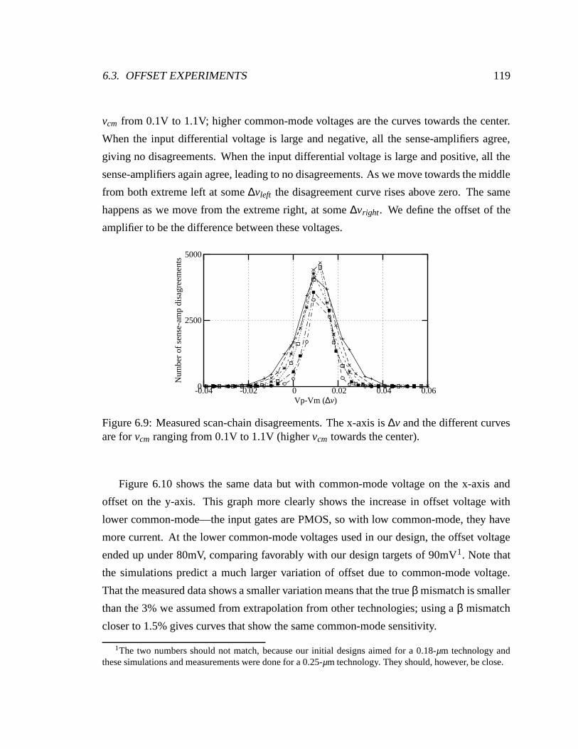
6.3. OFFSET EXPERIMENTS 119
vcm from 0.1V to 1.1V; higher common-mode voltages are the curves towards the center.
When the input differential voltage is large and negative, all the sense-amplifiers agree,
giving no disagreements. When the input differential voltage is large and positive, all the
sense-amplifiers again agree, leading to no disagreements. As we move towards the middle
from both extreme left at some ∆vleft the disagreement curve rises above zero. The same
happens as we move from the extreme right, at some ∆vright. We define the offset of the
amplifier to be the difference between these voltages.
Vp-Vm (∆v)
Num
ber
ofse
nse-
amp
disa
gree
men
ts
0.060.040.020-0.02-0.04
5000
2500
0
Figure 6.9: Measured scan-chain disagreements. The x-axis is ∆v and the different curvesare for vcm ranging from 0.1V to 1.1V (higher vcm towards the center).
Figure 6.10 shows the same data but with common-mode voltage on the x-axis and
offset on the y-axis. This graph more clearly shows the increase in offset voltage with
lower common-mode—the input gates are PMOS, so with low common-mode, they have
more current. At the lower common-mode voltages used in our design, the offset voltage
ended up under 80mV, comparing favorably with our design targets of 90mV1. Note that
the simulations predict a much larger variation of offset due to common-mode voltage.
That the measured data shows a smaller variation means that the true β mismatch is smaller
than the 3% we assumed from extrapolation from other technologies; using a β mismatch
closer to 1.5% gives curves that show the same common-mode sensitivity.
1The two numbers should not match, because our initial designs aimed for a 0.18-µm technology andthese simulations and measurements were done for a 0.25-µm technology. They should, however, be close.
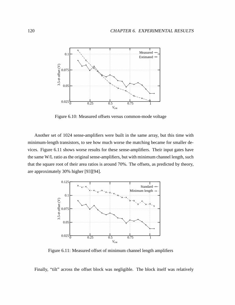
120 CHAPTER 6. EXPERIMENTAL RESULTS
EstimatedMeasured
Vcm
3.5-
σof
fset
(V)
10.750.50.250
0.1
0.075
0.05
0.025
Figure 6.10: Measured offsets versus common-mode voltage
Another set of 1024 sense-amplifiers were built in the same array, but this time with
minimum-length transistors, to see how much worse the matching became for smaller de-
vices. Figure 6.11 shows worse results for these sense-amplifiers. Their input gates have
the same W/L ratio as the original sense-amplifiers, but with minimum channel length, such
that the square root of their area ratios is around 70%. The offsets, as predicted by theory,
are approximately 30% higher [93][94].
Minimum lengthStandard
Vcm
3.5-
σof
fset
(V)
10.750.50.250
0.125
0.1
0.075
0.05
0.025
Figure 6.11: Measured offset of minimum channel length amplifiers
Finally, “tilt” across the offset block was negligible. The block itself was relatively

6.3. OFFSET EXPERIMENTS 121
small, leading to fairly uniform offsets across it. Figure 6.12 shows a three-dimensional plot
of the offsets by position; the random variation from sense-amp to sense-amp outweighs
any offset gradient across the bounding rectangle.
Offset voltage
0.040.02
0-0.02
Columns (64 total)
6050
4030
2010
0Rows (16 total) 14121086420
Figure 6.12: Measured offsets in their physical locations (in volts)
6.3.2 Systematic errors
In Figure 6.9, the center of the “hump,” where most of the sense-amplifier disagreements
occur, sits not at ∆v 0V, but rather closer to 10mV. This indicates that the sense-amplifiers
have some systematic offset, most likely due to imperfectly balanced layout. The ampli-
fiers were laid out carefully, but not carefully enough to avoid biases or offsets due to
manufacturing variations.
Figure 6.13 shows a plot of the sense-amplifier design from the polygon layout editor
Magic. Three layout features contribute to a systematic offset:
1. The tail device, at the center top of the diagram, ties the power supply to the tail
node, but then this current will flow both left and right to each of the input gates.
Metal misalignment may effectively move the tail device closer to one side than the
other. A dual-legged structure, with the tail device split between the two sides, would
avoid this problem, and would also allow the two input gates to be closer together,
eliminating any minor “tilt” in oxide thickness or implant across the amplifier.
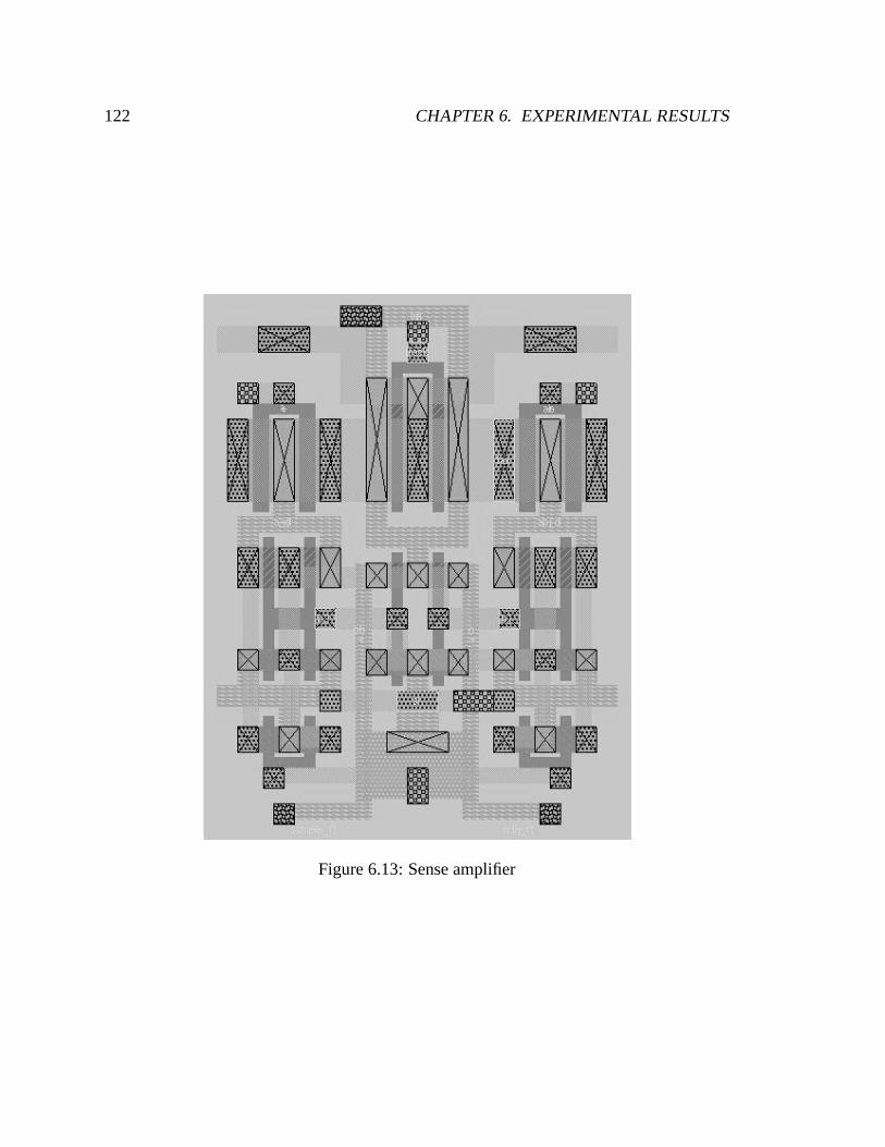
122 CHAPTER 6. EXPERIMENTAL RESULTS
Figure 6.13: Sense amplifier
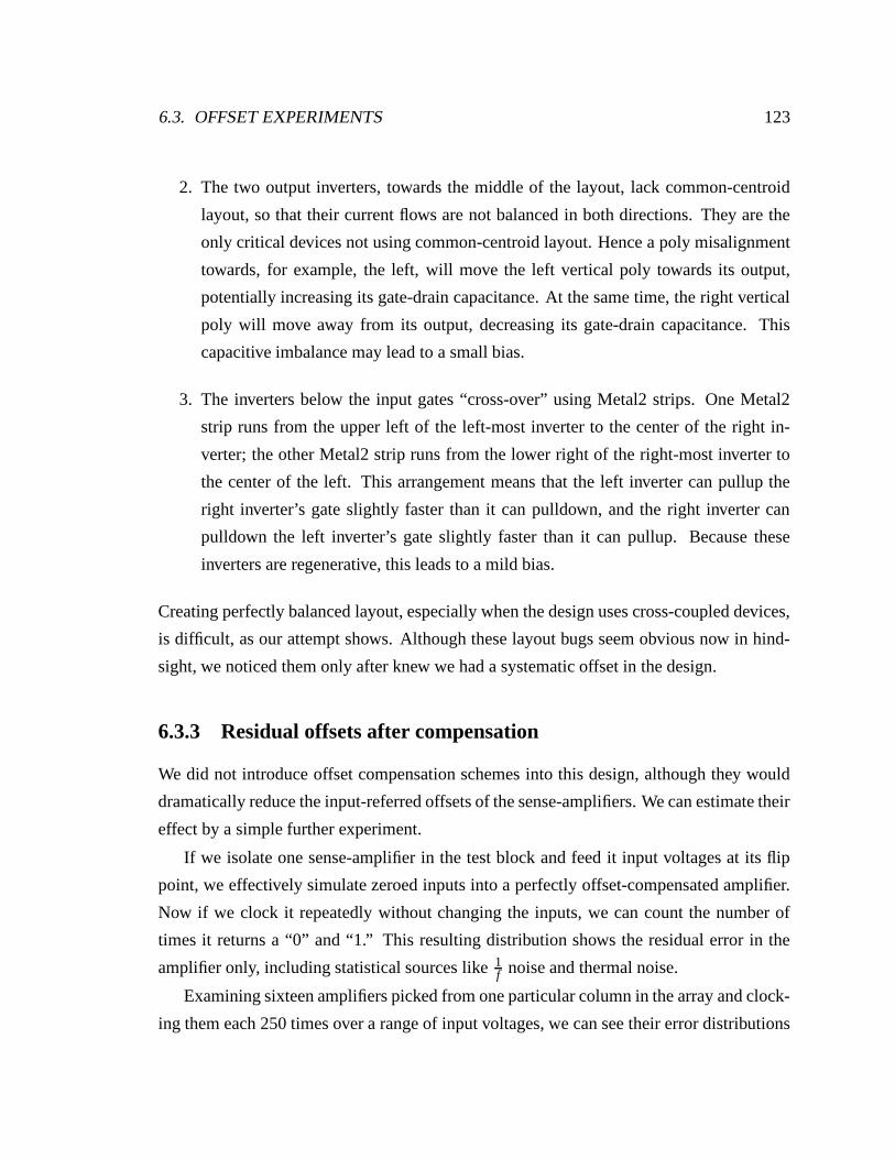
6.3. OFFSET EXPERIMENTS 123
2. The two output inverters, towards the middle of the layout, lack common-centroid
layout, so that their current flows are not balanced in both directions. They are the
only critical devices not using common-centroid layout. Hence a poly misalignment
towards, for example, the left, will move the left vertical poly towards its output,
potentially increasing its gate-drain capacitance. At the same time, the right vertical
poly will move away from its output, decreasing its gate-drain capacitance. This
capacitive imbalance may lead to a small bias.
3. The inverters below the input gates “cross-over” using Metal2 strips. One Metal2
strip runs from the upper left of the left-most inverter to the center of the right in-
verter; the other Metal2 strip runs from the lower right of the right-most inverter to
the center of the left. This arrangement means that the left inverter can pullup the
right inverter’s gate slightly faster than it can pulldown, and the right inverter can
pulldown the left inverter’s gate slightly faster than it can pullup. Because these
inverters are regenerative, this leads to a mild bias.
Creating perfectly balanced layout, especially when the design uses cross-coupled devices,
is difficult, as our attempt shows. Although these layout bugs seem obvious now in hind-
sight, we noticed them only after knew we had a systematic offset in the design.
6.3.3 Residual offsets after compensation
We did not introduce offset compensation schemes into this design, although they would
dramatically reduce the input-referred offsets of the sense-amplifiers. We can estimate their
effect by a simple further experiment.
If we isolate one sense-amplifier in the test block and feed it input voltages at its flip
point, we effectively simulate zeroed inputs into a perfectly offset-compensated amplifier.
Now if we clock it repeatedly without changing the inputs, we can count the number of
times it returns a “0” and “1.” This resulting distribution shows the residual error in the
amplifier only, including statistical sources like 1f noise and thermal noise.
Examining sixteen amplifiers picked from one particular column in the array and clock-
ing them each 250 times over a range of input voltages, we can see their error distributions
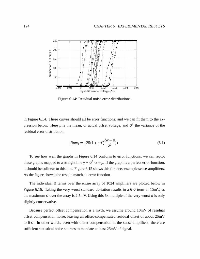
124 CHAPTER 6. EXPERIMENTAL RESULTS
Input differential voltage (∆v)
Num
ber
of1s
inou
tput
0.050.040.030.020.010-0.01-0.02
250
200
150
100
50
0
Figure 6.14: Residual noise error distributions
in Figure 6.14. These curves should all be error functions, and we can fit them to the ex-
pression below. Here µ is the mean, or actual offset voltage, and σ2 the variance of the
residual error distribution.
Num1 125
1
erf
∆v µσ2 (6.1)
To see how well the graphs in Figure 6.14 conform to error functions, we can replot
these graphs mapped to a straight line y σ2 x
µ. If the graph is a perfect error function,
it should be colinear to this line. Figure 6.15 shows this for three example sense-amplifiers.
As the figure shows, the results match an error function.
The individual σ terms over the entire array of 1024 amplifiers are plotted below in
Figure 6.16. Taking the very worst standard deviation results in a 6-σ term of 15mV, as
the maximum σ over the array is 2.5mV. Using this 6x multiple of the very worst σ is only
slightly conservative.
Because perfect offset compensation is a myth, we assume around 10mV of residual
offset compensation noise, leaving an offset-compensated residual offset of about 25mV
to 6-σ. In other words, even with offset compensation in the sense-amplifiers, there are
sufficient statistical noise sources to mandate at least 25mV of signal.
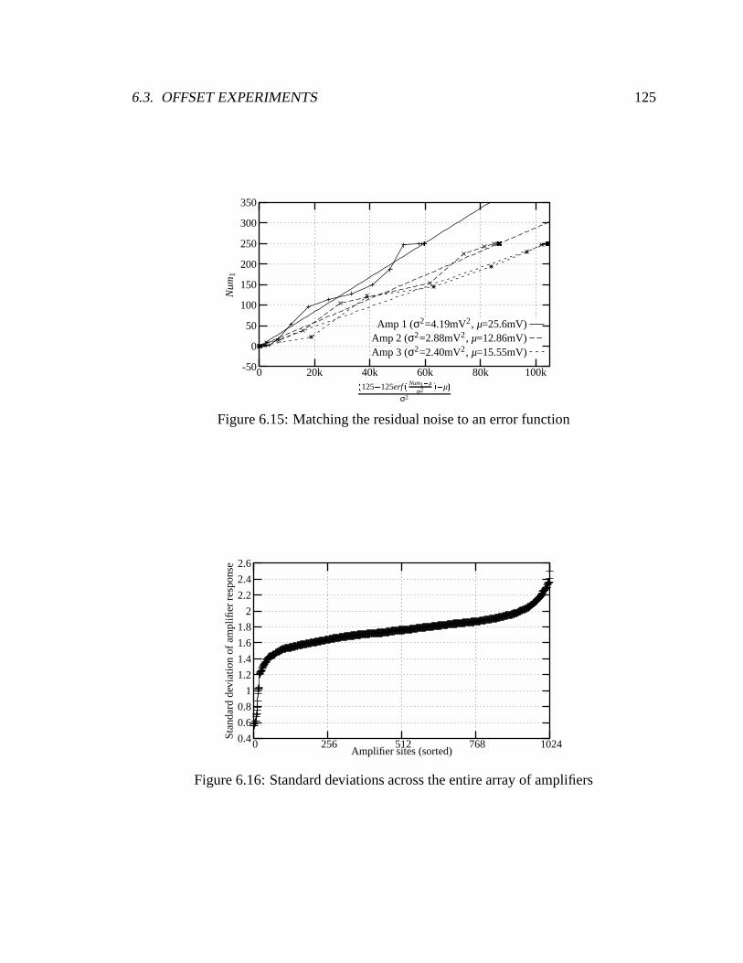
6.3. OFFSET EXPERIMENTS 125
Amp 3 (σ2=2.40mV2, µ=15.55mV)Amp 2 (σ2=2.88mV2, µ=12.86mV)
Amp 1 (σ2=4.19mV2, µ=25.6mV)
125 125erf
Num1 µ
σ2 µ σ2
Num
1
100k80k60k40k20k0
350
300
250
200
150
100
50
0
-50
Figure 6.15: Matching the residual noise to an error function
Amplifier sites (sorted)
Sta
ndar
dde
viat
ion
ofam
plifi
erre
spon
se
10247685122560
2.6
2.4
2.2
2
1.8
1.6
1.4
1.2
1
0.8
0.6
0.4
Figure 6.16: Standard deviations across the entire array of amplifiers
126 CHAPTER 6. EXPERIMENTAL RESULTS
6.3.4 Offset experiments we wish we had done
Ideally we could have varied the turn-on ramp rate of the amplifier’s tail device. Ramping
it extremely slowly negates capacitive imbalance in the device’s loads, and ramping it ex-
tremely quickly emphasizes any such capacitive imbalance. Adjusting the ramp rate would
have offered a way to measure this capacitive imbalance. Unfortunately, the clock driver
strength and power supply was fixed for the design.
Also, while measuring the residual noise in the sense-amplifier offers insight into the
system’s reliability, being able to measure the residual error response for a real channel
would be more interesting. In other words, doing the same experiment with real wires,
real crosstalk, and real noise-injecting inverters underneath the bus would have been more
realistic and thus more relevant. Unfortunately, we had no easy way of measuring residual
noise for a receiver on an unused bus somewhere else in the design.
6.4 Summary
This chapter described the implementation and measurements of a low-swing bus testchip.
One major experiment on the chip compared the energy requirements of several low-swing
buses of varying width and varying lengths to full-swing CMOS buses designed to provide
fair energy comparisons. When running at their target latency of 10 FO4 for a 10mm
on-chip hop, the full-swing buses were slightly throttled back from their top velocity, but
they also consumed an order of magnitude more energy than the low-swing buses. The
low-swing buses required negligible increased area.
A second major experiment, re-spun on a 0.25-µm technology to fix a logic error, de-
rived statistics for the intrinsic offset and mismatch for the sense-amplifiers used in the
design. Our design number of 90mV held up, as the mismatch to 3 5σ was under 80mV.
By repeatedly sampling sense-amps held at their offset-zeroed input voltages, we could
also determine the statistic residual noise to be 15mV at 6-σ.
The engineering challenges in building such a system are nontrivial. For example, our
sense-amplifiers, despite careful layout, still suffered from a systematic offset of about
10mV. Nonetheless, these experiments validated that not only could the low-swing system
6.4. SUMMARY 127
work in simulation, but also on a real chip, and with substantial energy savings.
Chapter 7
Conclusions
This work described the future of wires, and what designers can do about it. Wire delays
scale up as gate delays scale down. Understanding these trends quantitatively requires us
to forecast wire and gate characteristics and to combine them into performance metrics. In
Chapter 2 we used wire geometry information from the SIA roadmap to predict a range
of future wire resistances and capacitances; resistances scaled up linearly with time while
capacitances changed only slightly. Using a simple model for gate delays, we showed how
the ratio of wire delays to gate delays either scales slowly for scaled-length wires or grows
rapidly for fixed-length wires.
That future on-chip wires will display this duality, of “fast local wires” contrasted with
“slow global wires,” affects how we approach VLSI designs. Chapter 3 considered two
such design implications. First, CAD place-and-route tools must improve. With growing
die complexity and more local blocks gathered on a chip, maintaining constant design time
and designer productivity requires fewer wire exceptions per block and thus improved CAD
tools.
Second, modular architectures can effectively exploit the dual nature of wires. Fast
local wires in small compute cores, connected by slow but high-bandwidth wide global
buses, allow both high performance and high integration. Such modular architectures con-
nect their global wires into regular on-chip networks, using wide buses of high bandwidth
to offset long wire latencies.
128

129
Using such wide and long global buses can burn a great deal of power: the global net-
work in the Stanford Smart Memories modular architecture can consume up to 100W at
peak bandwidth, if built with traditional delay-optimal CMOS repeaters. Chapter 4 con-
siders the energy efficiency of such standard repeater architectures. By accepting a 10%
penalty in performance, traditional repeaters can be sized and spaced to save nearly 30% in
energy.
This 30% of energy savings is not a lot. Chapter 5 discusses techniques for running
global wires at a reduced voltage, thereby saving considerably more energy. Drivers us-
ing NMOS pullups and pulldowns swing differential twisted wires between ground and a
drive voltage significantly higher than the target voltage swing required by the receiver,
for decreased delay. Between transmitted bits, pre-equalization devices balance the dif-
ferential wires together; because we cannot overdrive this pre-equalization, we distribute
balance devices over the wire length. Receivers, made of simple latching amplifiers, use
the system clock, exploiting the synchronous nature of the global network. Their offsets
fundamentally limit how low of a swing we can use on the wires.
We roughed out these ideas in simulation, finding an order of magnitude in energy
savings for no effective slowdown of the Smart Memories global buses. Chapter 6 describes
the chip we built to more fully test these low-swing buses. This chip validated a 10x savings
in energy while running 10mm per clock phase. Another experiment validated our 90mV
offset estimates, and using that same experiment we could determine that if we had perfect
input offset compensation, the residual input uncertainty in the amplifier was still around
15mV. The test chip demonstrated that relatively simple low-swing architectures do work
and provide substantial energy savings for global on-chip buses.
This work can continue in many different directions. First, the low-swing architecture
can be modified to eliminate the receiver’s dependence on a global clock. By sending a
strobe signal along with the data we can self-time the wire system, although due to ramp-
up delay at the receiver this strobe signal will have to be sent slightly ahead of the data for
best performance. This allows some timing leeway in the global networks and if combined
with some form of handshaking between modules, can free the global network from a strict
relationship with the chip clock. Whether or not this flexibility is useful depends on the
system.
130 CHAPTER 7. CONCLUSIONS
Second, a careful reckoning of receiver offsets could both modify the existing design
as well as add offset compensation schemes. While the swing level is ultimately limited
by residual uncertainties (15mV in our design), this number is design-dependent as well.
Improving the receiver’s uncompensated offset as well as compensated residual uncertainty
would let us push the voltage swing and energy savings to extremes without worrying about
the non-scaling behavior of transistor offsets.
Third, formulating the low-swing ideas and techniques into a methodology or CAD
framework would dramatically improve its usability. Chip builders can be astonishingly
conservative, because the extra cost of more robust system components such as power
supplies or heat removers is much less than the cost of a yield drop or of field escapes due
to sensitive designs. In high-volume manufacturing, technical design considerations often
play second-fiddle to yield, manufacturing, and margins, so formalizing this exploratory
research will enhance its applicability.

Appendix A
Fanout in a buffered repeater
If we have a two inverters as a repeating stage, what should be the fanout between these
stages? Compare a fanout of four versus a fanout of one. The FO4 case has a longer
intrinsic delay and hence farther-spaced repeaters: fewer but slower stages. The FO1 case
has a shorter repeater delay and hence closer-spaced repeaters: more but faster stages.
Which is faster?
In any repeated system, if we think of a stage delay as broken into a gate-driving-
gate delay (“GateGate”), a gate-driving-wire delay (“GateWire”), a wire-driving-wire delay
(“WireWire”), and a wire-driving-gate delay (WireGate), we know that at the delay-optimal
length and driver size, we have
GateGate WireWire (A.1)
GateWire WireGate (A.2)
Let the fanout within the repeating stage be f . Then the GateGate delay is FO f
FO1
f , or, when normalized to a FO4,f
1
f
1 4 5 (assuming that diffusion ca-
pacitance is half of gate capacitance). Thus at the delay-optimal length, and assuming
center-skewed devices and a full power supply,
GateGate f
1
f
14 5 FO4 (A.3)
WireWire 0 35RwCwl2opt (A.4)
131

132 APPENDIX A. FANOUT IN A BUFFERED REPEATER
lopt
f
1
f
10 35 4 5
FO4RwCw
(A.5)
The other half of the story comes from equating the GateWire and WireGate delays.
Because of the repeater’s internal fanout, the gate drive is f times more powerful than its
input capacitance would indicate:
GateWire Rv
f woptCwlopt (A.6)
WireGate Rwlopt3Cgwopt (A.7)
wopt
RvCw
3 f RwCg(A.8)
Rewriting and then dividing the stage delay by lopt for delay per unit-length gives us
the following. Note that all of this can be restated by using the general repeater model with
a 3, b 1 5 f , r 1
f , and d
f
0 5 4 5.
GateWire 0 360f
1
f
1f
FO4 (A.9)
Delay/unit-length ∝
f
1
f
12
1f
(A.10)
We can also specify the energy of a buffer by using e 3f
0 5 , giving a total energy
of
Energy ∝ 1
1 5 f
12f 2
f
1 (A.11)
Whether we consider just delay, or the energy delay product, the optimal fanouts sit
around 2.25–2.5, with fairly low sensitivity. This doesn’t change much with other l or w
design points, either. At an energy delay optimal of l 1 5 and w 0 4, the optimal fanout
is still between 2.5 and 3.
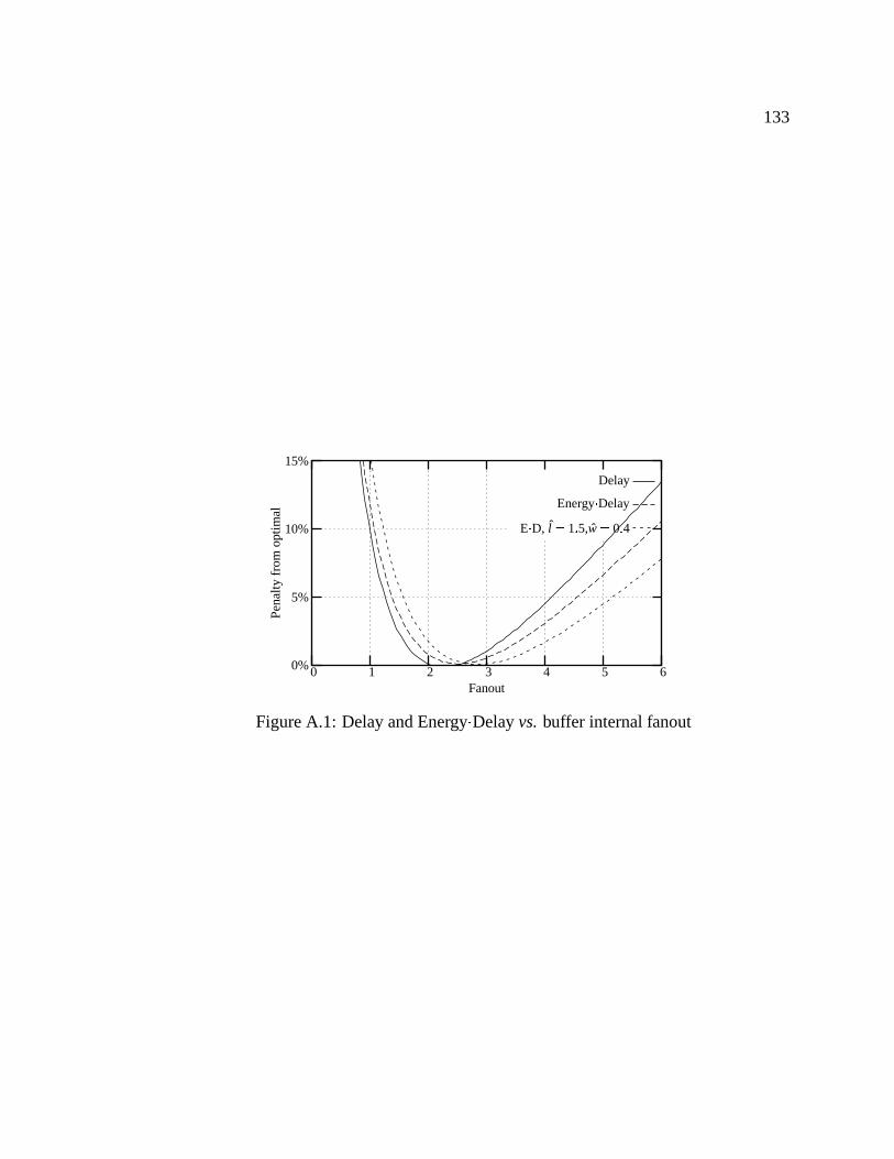
133
E D, l 1 5,w 0 4
Energy Delay
Delay
Fanout
Pen
alty
from
opti
mal
6543210
15%
10%
5%
0%
Figure A.1: Delay and Energy Delay vs. buffer internal fanout

Bibliography
[1] K. Saraswat et al., “Effect of Interconnection Scaling on Time Delay of VLSI Cir-
cuits,” IEEE Transactions on Electron Devices, pp. 645-50, April 1982.
[2] J. Meindl, Georgia Tech, comments at SRC/Marco Workshop, held at the Center for
Integrated Systems, Stanford University, May 1999.
[3] A. Brand et al., “Intel’s 0.25 Micron, 2.0 Volts Logic Process Technology,” Intel
Technical Journal, Volume 2, Issue 3, August 1998.
[4] S. Thompson et al., “130nm Logic Technology Featuring 60nm Transistors, Low-K
Dielectrics, and Cu Interconnects,” Intel Technical Journal, Volume 6, Issue 2, May
2002.
[5] P. Kapur et al., “Technology and reliability constrained future copper interconnects:
Resistance modeling,” IEEE Transaction on Electron Devices, pp. 590-7, April 2002.
[6] Semiconductor Industry Association, International Technology Roadmap for Semi-
conductors, 1999.
[7] T. Williams, Morphics, private communication, 2000.
[8] M. Bohr, “Interconnect Scaling—The Real Limiter to High Performance ULSI,”
Technical Digest, International Electron Devices Meeting, pp. 241-4, December
1995.
[9] Y. Nishi, “The Trend of On-Chip Interconnects: An International Perspective,” Pre-
sented at Stanford University, Spring Seminar Series, 1998.
134

BIBLIOGRAPHY 135
[10] L. Pillegi, Carnegie-Mellon University, private communication, 1999.
[11] A. Ruehli, “Inductance calculations in a complex integrated circuit environment,”
IBM Journal of Research and Development, No. 5, pp. 470-81, September 1972.
[12] E. Rosa, “The self and mutual inductance of linear conductors,” Bulletin of the
National Bureau of Standards, pp. 301-344, 1908.
[13] M. Kamon et al., “FastHenry: A Multipole-Accelerated 3-D Inductance Extraction
Program,” IEEE Transactions on Microwave Theory and Techniques, pp. 1750-8,
September 1994.
[14] M. Beattie et al., “IC Analyses Including Extracted Inductance Models,” Proceedings
of the Design Automation Conference, pp. 915-20, June 1999.
[15] K. Shepard et al., “Return-Limited Inductance: A Practical Approach to On-Chip
Inductance Extraction,” Proceedings of the IEEE Custom Integrated Circuits Confer-
ence, pp. 453-6, May 1999.
[16] A. Deutsch et al., “The importance of inductance and inductive coupling for on-chip
wiring,” 6th Topical Meeting of the Electrical Performance of Electronic Packaging,
pp. 53-6, October 1997.
[17] P. Restle et al., “Designing the Best Clock Distribution Network,” Digest of Technical
papers, Symposium on VLSI Circuits, pp. 2-6, June 1998.
[18] B. Krauter et al., “Including Inductance Effects in Interconnect Timing Analysis,”
Proceedings of the IEEE Custom Integrated Circuits Conference, pp. 445-52, May
1999.
[19] D.A.B. Miller, “Rationale and challenges for optical interconnects to electronic
chips,” Proceedings of the IEEE, pp. 728-49, June 2000.
[20] T. Ghani et al., “100 nm gate length high performance/low power CMOS transis-
tor structure,” Technical Digest, International Electron Devices Meeting, pp. 415-8,
December 1999.

136 BIBLIOGRAPHY
[21] A. Vittal et al., “Crosstalk reduction for VLSI,” IEEE Transactions on Computer-
Aided Design, pp. 290-8, March 1997.
[22] T. Sato et al., “Accurate In-situ Measurement of Peak Noise and Signal Delay Induced
by Interconnect Coupling,” Digest of Technical Papers, IEEE International Solid-
State Circuits Conference, pp. 226-7, February 2000.
[23] K. Soumyanath et al., “Accurate on-chip interconnect evaluation: A time-domain
technique,” IEEE Journal of Solid-State Circuits, pp. 623-31, May 1999.
[24] L. Pillagi et al., “Asymptotic Waveform Evaluation for Timing Analysis,” IEEE
Transactions on Computer-Aided Design, pp. 352-66, April 1990.
[25] S. Morton, “On-chip Inductance Issues in Multiconductor Systems,” Proceedings of
the Design Automation Conference, pp. 921-6, June 1999.
[26] S. Naffziger, “Design Methodologies for Interconnect in GHz+ ICs,” Tutorial, IEEE
International Solid-State Circuits Conference, February 1999.
[27] L. He et al., “An Efficient Inductance Modeling for On-chip Interconnects,” Proceed-
ings of the Custom Integrated Circuits Conference, pp. 457-60, May 1999.
[28] D. Priore, “Inductance on silicon for sub-micron CMOS VLSI,” Digest of Technical
Papers, Symposium on VLSI Circuits, pp. 17-18, June 1993.
[29] C. Hu, “CMOS Transistor Scaling Limits,” invited talk, Proceedings of the Design
Automation Conference, June 2000.
[30] G. Moore, “No Exponential Is Forever: But Forever Can Be Delayed,” Keynote
address, IEEE International Solid-State Circuits Conference, February 2003.
[31] T. Lin et al., “A Fully Planarized 6-Level-Metal CMOS Technology for 0.25-0.18
Micron Foundry Manufacturing,” Technical Digest, International Electron Devices
Meeting pp. 851-4, December 1997.
[32] D. Harris, Skew-Tolerant Circuit Design, Morgan Kaufman, 2000.

BIBLIOGRAPHY 137
[33] E. Sprangle et al., “Increasing processor performance by implementing deeper
pipelines,” Proceedings of the 29th International Symposium on Computer Archi-
tecture, May 2002.
[34] M. Hrishikesh et al., “The optimal logic depth per pipeline stage is 6 to 8 FO4 inverter
delays,” Proceedings of the 29th International Symposium on Computer Architecture,
pp. 14-24, May 2002.
[35] V. Srinivasan et al., “Optimizing Pipelines for Power and Performance,” 35th Inter-
national Symposium on Microarchitecture, November 2002.
[36] P. Green, “A GHz IA-32 architecture microprocessor implemented on 0.18 µm tech-
nology with aluminum interconnect,” Digest of Technical Papers, IEEE International
Solid-State Circuits Conference, pp. 98-99, February 2000.
[37] Semiconductor Industry Association, International Technology Roadmap for Semi-
conductors, 2002 update, 2002.
[38] W. Song et al., “Power Distribution Techniques for VLSI Circuits,” in Proceedings,
Conference on Advanced Research in VLSI, pp. 45-52, January 1984.
[39] F.W. Grover, Inductance Calculations Working Formulas and Tables, Dover Publica-
tions, 1946.
[40] Y. Massoud et al., “Layout Techniques for Minimizing On-Chip Interconnect Self
Inductance,” Proceedings of the Design Automation Conference, pp. 566-71, June
1998.
[41] M. Ang et al., “An On-Chip Voltage Regulator Using Switched Decoupling Capac-
itors,” Digest of Technical Papers, IEEE International Solid-State Circuits Confer-
ence, pp. 438-9, February 2000.
[42] R. Ho et al., “Scaling implications for CAD,” Proceedings of the International
Conference on Computer-Aided Design, pp 425-9, November 1999.
138 BIBLIOGRAPHY
[43] W. Donath, “Placement and Average Interconnections Lengths of Computer Logic,”
IEEE Transactions on Circuits and Systems, CAS-26, pp. 272-277, April 1979.
[44] J. Davis et al., “A Stochastic Wire-Length Distribution for Gigascale Integration –
Part I: Derivation and Validation,” IEEE Transactions on Electron Devices, Volume
45, No. 3, pp. 580-9, March 1998.
[45] S. Keckler et al., “The MIT Multi-ALU Processor,” HotChips IX Digest, pp. 1-7,
August 1997.
[46] J. Kuskin et al., “The Stanford FLASH Multiprocessor,” Proceedings of the 21st
International Symposium on Computer Architecture, pp. 302-13, April 1994.
[47] NVIDIA corporation, brochure/literature from booth at Design Automation Confer-
ence, August 2002.
[48] Private communication, D. Halvorson, Intel Corporation, on trends noted at the De-
sign Automation Conference, August 2002.
[49] D. Sylvester et al., “Getting to the Bottom of Deep Submicron,” Proceedings of the
International Conference on Computer-Aided Design, November 1998.
[50] H. Kapadia et al., “Using Partitioning to Help Convergence in the Standard-Cell De-
sign Automation Methodology,” Proceedings of the Design Automation Conference,
August 1999.
[51] H. Kapadia, “Partition-Driven Convergence in the Design of Random-Logic Blocks,”
Ph.D. Thesis, Stanford University, 2000.
[52] J. Stinson et al., “A 1.5GHz Third Generation Itanium Processor,” Digest of Techni-
cal Papers, IEEE International Solid-State Circuits Conference, pp. 252-3, February
2003.
[53] S. Naffziger el al., “The Implementation of the Next-Generation 64b Itanium Mi-
croprocessor,” Digest of Technical Papers, IEEE International Solid-State Circuits
Conference, February 2002.
BIBLIOGRAPHY 139
[54] V. Agarwal et al., “Clock rate versus IPC: The end of the road for conventional
microprocessors,” Proceedings of the 27th International Symposium on Computer
Architecture, pp. 248-59, June 2000.
[55] W. Dally et al., “VLSI architecture: Past, present, and future,” Proceedings of the
Conference on Advanced Research in VLSI, pp. 232-41, January 1999.
[56] E. Chiprout et al., Asymptotic Waveform Evaluation, Kluwer Academic Publishers,
1994.
[57] D. Sylvester et al., “Getting to the bottom of deep submicron II: a global wiring
paradigm,” in Proc. ISPD, pp. 193-200, April 1999.
[58] P. Fisher et al., “Clock Cycle Estimation and Test Challenges for Future Micropro-
cessors,” Sematech Technology Transfer document #98033484A-TR, May 1998.
[59] B. A. Gieseke et al., “A 600 MHz superscalar RISC microprocessor with out-of-
order execution,” Digest of Technical Papers, IEEE International Solid-State Circuits
Conference, pp. 176-7, February 1997.
[60] M. Taylor et al., “A 16-Issue Multiple Program Counter Microprocessor with Point-
to-Point Scalar Operand Networks,” Digest of Technical Papers, IEEE International
Solid-State Circuits Conference, pp. 170-1, February 2003.
[61] S. Keckler et al., “A Wire-Delay Scalable Microprocessor Architecture for High-
Performance Systems,” Digest of Technical Papers, IEEE International Solid-State
Circuits Conference, February 2003.
[62] K. Mai et al., “Smart Memories: A Modular Reconfigurable Architecture,” Proceed-
ings of the 27th International Symposium on Computer Architecture, pp. 161-71, June
2000.
[63] TSMC presentation at Stanford University Electrical Engineering Seminar Series,
Spring 2001.
140 BIBLIOGRAPHY
[64] H. Bakoglu, Circuits, Interconnections and Packaging for VLSI, Addison-Wesley,
1990.
[65] K. Nose et al., “Power-Conscious Interconnnect Buffer Optimization with Improved
Modeling of Driver MOSFET and Its Implications to Bulk and SOI CMOS Technol-
ogy,” in ISPLED, pp. 24-29, Aug. 2002.
[66] M. Stan et al., “Low-Power Encodings for Global Communication in CMOS VLSI,”
IEEE Trans. VLSI Systems, pp. 444-55, Dec. 1997.
[67] J. Tabor, “Noise Reduction Using Low-Weight and Constant-Weight Coding Tech-
niques,” M.S. Thesis, MIT, 1990.
[68] M. Stan et al., “Bus-Invert Coding For Low-Power I/O,” IEEE Trans. VLSI Systems,
pp. 49-58, Mar. 1995.
[69] K. Nakamura et al., “A 50% Noise Reduction Interface Using Low-Weight Coding,”
in VLSI Circuits Symp. Dig. Tech. Papers, pp. 144-5, Jun. 1996.
[70] P. Sotiriadis et al., “Reducing Bus Delay In Submicron Technology Using Coding,”
in Proc. of the ASP-DAC, pp. 109-114, 2001.
[71] F. Dartu et al., “TETA: transistor-level engine for timing analysis,” Proceedings of
the Design Automation Conference, pp. 595-8, June 1998.
[72] R. Arunchalam et al., “CMOS gate delay models for general RLC loading,” in Pro-
ceedings, IEEE International Conference on Computer Design, pp. 224-9, October
1997.
[73] I. Sutherland et al., Logical Effort: Designing Fast CMOS Circuits, Morgan Kauf-
mann, January 1999.
[74] S. Sze, editor, VLSI Technology, McGraw-Hill, p. 482, 1988.
[75] K. Mai et al., “Low-Power SRAM Design Using Half-Swing Pulse-Mode Tech-
niques,” IEEE Journal of Solid-State Circuits, pp. 1659-71, Nov. 1998.
BIBLIOGRAPHY 141
[76] Y. Nakagome et al., “Sub-1-V swing bus architecture for future low-power ULSIs,”
Digest of Technical Papers, Symposium on VLSI Circuits, pp. 82-3, June 1992.
[77] R. Golshan et al., “A novel reduced swing CMOS BUS interface circuit for high speed
low power VLSI systems,” in Proc. IEEE Int’l Symposium on Circuits and Systems,
pp. 351-4, May 1994.
[78] B.-D. Yang et al., “High-Speed and Low-Swing On-Chip Bus Interface Using Thresh-
old Voltage Swing Driver and Dual Sense Amplifier Receiver,” in Proc. European
Solid-State Circuit Conference, pp. 144-7, September 2000.
[79] H. Zhang et al., “Low-swing on-chip signaling techniques,” IEEE Transactions on
VLSI, pp. 414-419, April 1993.
[80] G. Cardarilli et al., “Bus architecture for low-power VLSI digital circuits,” in Proc.
IEEE Int’l Symposium on Circuits and Systems, pp. 21-24, May 1996.
[81] A. Rjoub et al., “Efficient Drivers, Receivers, and Repeaters for Low Power CMOS
Bus Architectures,” in Proceedings of the International Conference on Electronics,
Circuits and Systems, pp. 789-94, 1999.
[82] E.D. Kyriakis-Bitzaros, “Design of low power CMOS drivers based on charge re-
cycling,” in Proc. IEEE Int’l Symposium on Circuits and Systems pp 1924-7, June
1997.
[83] M. Hiraki et al., “Data-Dependent Logic Swing Internal Bus Architecture for
Ultralow-Power LSIs,” IEEE Journal of Solid-State Circuits, pp. 397-402, Apr. 1995.
[84] A. Bellaouar et al., “An ultra-low-power CMOS on-chip interconnect architecture,”
in Proc. ISPLED, pp. 52-3, 1995.
[85] J. Yuan, “Low Power and Low Area or High Throughput Single-Ended Bus and I/O
Protocols,” in Proc. IEEE Int’l Sympsosium on Circuits and Systems, pp. 1932-5, Jun.
1997.

142 BIBLIOGRAPHY
[86] H. Yamauchi et al., “An Asymptotically Zero Power Charge-Recycling Bus Architec-
ture for Battery-Operated Ultrahigh Data Rate ULSIs,” IEEE Journal of Solid-State
Circuits, pp. 423-31, Apr. 1995.
[87] Y. Nakase et al., “Complementary half-swing bus architecture and its application for
wide-band SRAM macros,” IEE Proc. Circuits Devices Syst., pp. 337-342, Oct. 1998.
[88] W. Dally et al., “A Single-Chip Terabit Switch,” Hot Chips 13, 2001.
[89] H. Kojima et al., “Half-swing clocking scheme for 75% power saving in clocking
circuitry,” IEEE Journal of Solid-State Circuits, pp. 432-5, April 1995.
[90] M. Karlsson et al., “Low-swing charge recycle bus drivers,” in Proc. Int’l Symposium
on Circuits and Systems, pp. 117-120, May 1998.
[91] T. Burd, “Energy-Efficient Processor System Design,” Ph.D. Thesis, University of
California Berkeley, 2001.
[92] B. Nikolic et al., “Improved Sense Amplifier-Based Flip-Flop: Design and Measure-
ments,” IEEE Journal of Solid State Circuits, Vol. 35, pp. 876-84, June 2000.
[93] M. Pelgrom et al., “Matching Properties of MOS Transistors,” IEEE Journal of Solid-
State Circuits, pp. 1433-40, October 1989.
[94] Lovett et al., “Optimizing MOS Transistor Mismatch,” IEEE Journal of Solid-State
Circuits, p. 147-50, January 1998.
[95] C. Svensson, “Optimum Voltage Swing on On-Chip and Off-Chip Interconnect,”
IEEE Journal of Solid-State Circuits, pp. 1108-12, Jul. 2001.
[96] I. Sutherland et al., “Designing fast asynchronous circuits,” Asynchronous Circuits
and Systems, pp. 184-93, March 2001.
[97] Y. Mosiadis et al., “High Performance Level Restoration Circuits for Low-Power
Reduced-Swing Interconnect Systems,” in Proc. IEEE Int’l Conference on Electron-
ics, Circuits, and Systems, pp. 619-22, Dec. 2000.
BIBLIOGRAPHY 143
[98] R. Ho, et al.“Applications on On-Chip Samplers for Test and Measurement of Inte-
grated Circuits,” Digest of Technical Papers, Symposium on VLSI Circuits, pp. 138-9,
June 1998.
[99] Semiconductor Industry Association, National Technology Roadmap for Semicon-
ductors, 1997.