Embed Size (px)
Citation preview
CADENCE CONFIDENTIAL1 CADENCE DESIGN SYSTEMS, INC.
On-chip RF Isolation Techniques
Tallis Blalack, Youri Leclercq, Patrick Yue1
1Atheros Communications, Inc.
BCTM 12.1 October 1, 2002

2 Tallis Blalack, BCTM 2002, Paper 12.1
Key Take-away Point
IT DEPENDS!
� What is the maximum isolation I can achieve?
� How do I win the isolation argument with my co-workers?
� Will I get anything useful out of this talk?

3 Tallis Blalack, BCTM 2002, Paper 12.1
Outline
� Technology impacts� Technology overview� Buried layers� Triple wells
� Grounding effects� Guard rings� Shielding
� Patterned ground shield
� On-chip decoupling capacitance� Summary

4 Tallis Blalack, BCTM 2002, Paper 12.1
Lightly-Doped Wafer Resistivity
TWafer d = TWafer TWafer1 2
TWafer
RSubstrate
1 2
Non-conductive Backside

5 Tallis Blalack, BCTM 2002, Paper 12.1
Lightly-Doped Wafer Resistivity
TWafer
d = 2.5 x TWafer1 2
Non-conductive Backside
1 2RA RB
k * d
RA

6 Tallis Blalack, BCTM 2002, Paper 12.1
Lightly-Doped Wafer Resistivity
1 2d « TWafer
TWafer
RSubstrate
1 2
d2 = 2 * d1 : R2 < 2 * R1
Non-conductive Backside
7 Tallis Blalack, BCTM 2002, Paper 12.1
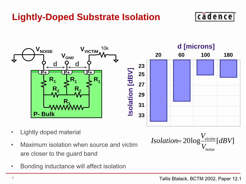
Lightly-Doped Substrate Isolation
� Lightly doped material
� Maximum isolation when source and victim are closer to the guard band
� Bonding inductance will affect isolation
27
25
29
31
33
23
Isol
atio
n [d
BV]
][log20 dBVVVIsolation
noise
victim=
P- Bulk
VNOISE
R1
R3
R2
VVICTIM
P+P+
VGND
P+R1 R1
R2
dd
10k d [microns]20 60 100 180

8 Tallis Blalack, BCTM 2002, Paper 12.1
Lightly-Doped Wafer Resistivity
1 2d « TWafer
TWafer
RSubstrate
1 2
d2 = 2 * d1 : R2 < 2 * R1
Floating Conductive Backside

9 Tallis Blalack, BCTM 2002, Paper 12.1
Lightly-Doped Wafer Resistivity
TWafer d = TWafer TWafer1 2
TWafer
RSubstrate
1 2
Floating Conductive Backside

10 Tallis Blalack, BCTM 2002, Paper 12.1
Lightly-Doped Wafer Resistivity
TWafer
d = 2.5 x TWafer1 2
RB
= 0
Floating Conductive Backside
1 2RA RA

11 Tallis Blalack, BCTM 2002, Paper 12.1
BiCMOS Technology Basics
p- substrate(~12 ohm-cm)
field implant(~0.2 ohm-cm)
p
T pro
cess
well(~1 ohm-cm)
n
contact(~0.005 ohm-cm)
p+buriedlayer
(~0.005ohm-cm)
n+p+
sinker(~0.005 ohm-cm)
p+
deeptrench
F. Clement in J. Huijsing et al, KAP, �99

12 Tallis Blalack, BCTM 2002, Paper 12.1
Buried Layer with Lightly-Doped Wafers
p- wafer(~12 ohm-cm)
Tbulk (~400 um)
Tepi (~3 um)
Tburied (~1 um)
p epitaxial layer(~1 ohm-cm)
p+ buried layer(~0.005 ohm-cm)
Rbulkepi ~ 5 x Rburied
13 Tallis Blalack, BCTM 2002, Paper 12.1
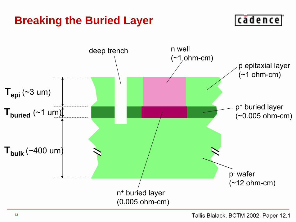
Breaking the Buried Layer
p- wafer(~12 ohm-cm)
Tbulk (~400 um)
Tepi (~3 um)
Tburied (~1 um)
n+ buried layer(0.005 ohm-cm)
n well(~1 ohm-cm)
deep trench
p epitaxial layer(~1 ohm-cm)
p+ buried layer(~0.005 ohm-cm)

14 Tallis Blalack, BCTM 2002, Paper 12.1
Sony: 622 Mb/s Optical Receiver IC
T. Takeshita, ISSCC 2002

15 Tallis Blalack, BCTM 2002, Paper 12.1
Sony Noise Simulation
trans-impedanceamplifier
W: 50 µmW: 10 µm
N- layer breaking buried layersubstrate contact
� Substrate noise distribution� SubstrateStorm
� Noise source injection points� Logic ground
� Noise source amplitude of 100%
Double-guardNo guard ring
1% 0.05%20x noise reduction
1.65 to 100%1.45 to 1.65%1.25 to 1.45%1.05 to 1.25%0.85 to 1.05%
Noise amplitudeat substrate
0.65 to 0.85%0.45 to 0.65%0.25 to 0.45%0.05 to 0.25%0.00 to 0.05%
16 Tallis Blalack, BCTM 2002, Paper 12.1
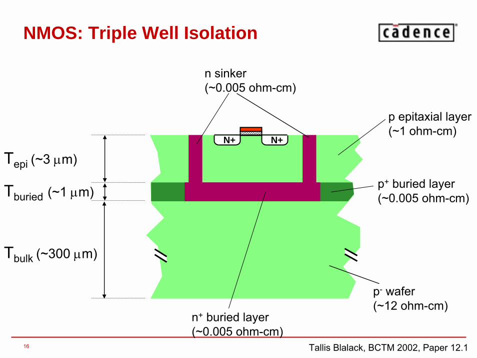
NMOS: Triple Well Isolation
p- wafer(~12 ohm-cm)
Tbulk (~300 µm)
Tepi (~3 µm)
Tburied (~1 µm)
n sinker(~0.005 ohm-cm)
N+N+
p epitaxial layer(~1 ohm-cm)
p+ buried layer(~0.005 ohm-cm)
n+ buried layer(~0.005 ohm-cm)

17 Tallis Blalack, BCTM 2002, Paper 12.1
Motorola: GSM/GPRS Baseband IC
Nwellipw
Analog
Nwell
Digital
P+ Substrate
Nwell
VDD VSS
ipw
Isolation Strategy
Benefits of IPW isolation
VDD VSS
D. Redmond, ISSCC 2002
Triple wellGuard ringReference
Process technology HiP7LP : (compatible with TSMC)
Gate length Lpoly 0.13 µmSingle gate Ox 30 ADual gate Ox 50 ASupply voltage 1.6 to 3.0 VMetal 5 layer CuSubstrate P+Nwell resistors 700 ohm/sqSalicided Poly res. 7.0 ohm/sqMetal Cap 0.8 fF/µm2

18 Tallis Blalack, BCTM 2002, Paper 12.1
Triple-well Simulation Structure
Vss
Vccor
Vdd180 µm
Noise from inverter core
Triple well Sensor
1000 µmVcc
� Separate ground used for the digital core
� All simulations use SubstrateStorm with a 0.35 µm BiCMOS technology
� Remove triple well and compare with identical p+ guard ring

19 Tallis Blalack, BCTM 2002, Paper 12.1
Package Effects on Triple-well IsolationGuard Ring and Triple Well Isolation vs. Frequency
-120
-110
-100
-90
-80
-70
-60
-50
-40
0.E+00 2.E+09 4.E+09 6.E+09 8.E+09 1.E+10Frequency (Hz)
Atte
nuat
ion
(dB
)
TW_Vcc_0.5nH Ring_0.5nH TW_Vdd_0.5nHRing_0nH TW_Vdd_0nH

20 Tallis Blalack, BCTM 2002, Paper 12.1
Grounding Effects
P- Bulk
P+
Vsub1
Rbulk
Risolation
Rbulk
Vsub2Substrate Contacts
P+P+P+
Substrate Contacts
� Use multiple supplies to isolate areas
� Minimize inductance

21 Tallis Blalack, BCTM 2002, Paper 12.1
STMicroelectronics: LNA + Mixer Integration
� Initial design had one substrate ground
� Simulations showed too much noise coupling
� Separated supply regions to isolate LNA from mixer
One substrate ground Two substrate groundsA. Cathelin, DATE 2002

22 Tallis Blalack, BCTM 2002, Paper 12.1
Coupling Paths
ANALOG
DIGITALNoisy
Sensitive
Asub
Dsub
Substratecontacts
R1
R2
Equivalent behavior with pad or seal ring !!!

23 Tallis Blalack, BCTM 2002, Paper 12.1
Guard Rings in a Lightly-Doped Process
P- Bulk
N+N+P+ P+ P+N+
N Well
DGndAGnd
P channelstop implant
AVdd
� Guard rings are more effective in a lightly doped process
� A well region can break the channel stop and increase the isolation

24 Tallis Blalack, BCTM 2002, Paper 12.1
Guard Ring Inductance Simulation Structure
45 µm wide
sensor
VssL
10 µm guardring
Noise from inverter core
1000 µm

25 Tallis Blalack, BCTM 2002, Paper 12.1
Guard Ring Inductance Simulations
Inductance Effects on Guard Ring Isolation (W = 10 µm)
-120
-110
-100
-90
-80
-70
-60
0.E+00 2.E+09 4.E+09 6.E+09 8.E+09 1.E+10Frequency (Hz)
Atte
nuat
ion
(dB
)
No Guard Ring L = 0.5 nH L = 0.3 nH L = 0.1 nH

26 Tallis Blalack, BCTM 2002, Paper 12.1
Ericsson & STMicroelectronics: Single-chip BLUETOOTH ASIC
300 µm wide P+ guard band
� 0.18 µm CMOS� 2.5 � 3.0 V� 75 mW in RX� 90 mW in TX� 2 MHz IF� 5 GHz VCO� 5.5 mm2
� Special attention to crosstalk
P. van Zeijl, ISSCC 2002

27 Tallis Blalack, BCTM 2002, Paper 12.1
Guard Ring Width Simulation Structure
Vss0.3 nH
10 µm wide
spacing
Noise from inverter core
Guardring Sensor
1000 µm
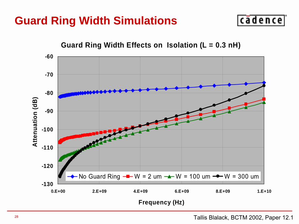
28 Tallis Blalack, BCTM 2002, Paper 12.1
Guard Ring Width Simulations
Guard Ring Width Effects on Isolation (L = 0.3 nH)
-130
-120
-110
-100
-90
-80
-70
-60
0.E+00 2.E+09 4.E+09 6.E+09 8.E+09 1.E+10
Frequency (Hz)
Atte
nuat
ion
(dB
)
No Guard Ring W = 2 um W = 100 um W = 300 um

29 Tallis Blalack, BCTM 2002, Paper 12.1
Guard Ring Isolation Summary
The maximum achievable guard ring isolation is ?
Dependent on:
� Technology
� Spacing
� Width
� Grounding scheme
� Package parasitics
� �
30 Tallis Blalack, BCTM 2002, Paper 12.1
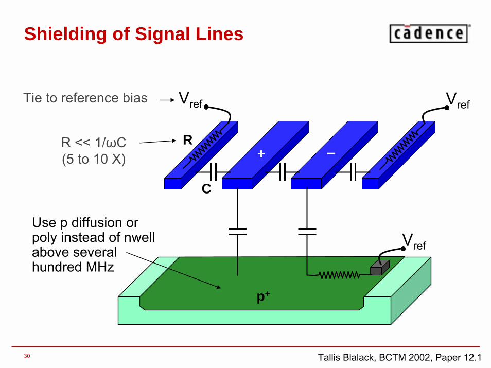
Shielding of Signal Lines
p+
+ –
Vref
VrefVref
C
R
Use p diffusion or poly instead of nwell above several hundred MHz
Tie to reference bias
R << 1/ωC(5 to 10 X)

31 Tallis Blalack, BCTM 2002, Paper 12.1
Patterned Ground Shield Design
� Pattern
� Orthogonal to spiral
(induced loop current)
� Resistance
� Low for termination of the electric field
� Avoid attenuation of the magnetic field

32 Tallis Blalack, BCTM 2002, Paper 12.1
Q Improvement – Tank Impedance Doubled
33 Tallis Blalack, BCTM 2002, Paper 12.1
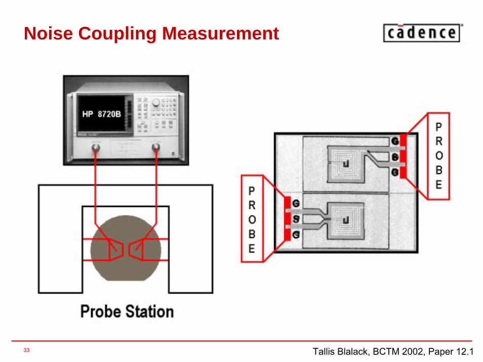
Noise Coupling Measurement

34 Tallis Blalack, BCTM 2002, Paper 12.1
Effect of Polysilicon Ground Shield on Noise Coupling
35 Tallis Blalack, BCTM 2002, Paper 12.1
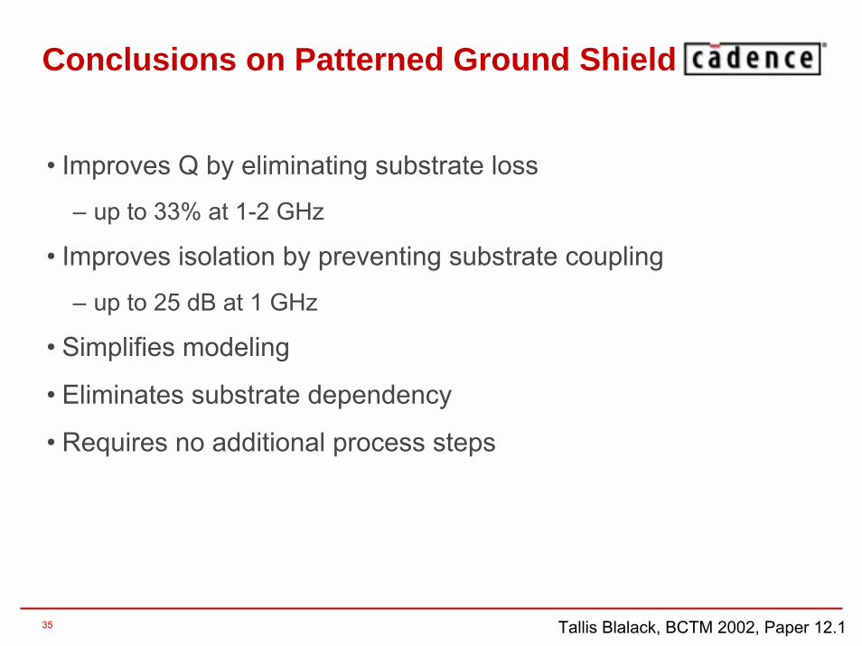
Conclusions on Patterned Ground Shield
� Improves Q by eliminating substrate loss
� up to 33% at 1-2 GHz
� Improves isolation by preventing substrate coupling
� up to 25 dB at 1 GHz
� Simplifies modeling
� Eliminates substrate dependency
� Requires no additional process steps

36 Tallis Blalack, BCTM 2002, Paper 12.1
Atheros: 802.11a Radio Transceiver
� 0.25 µm standard digital CMOS for 5 GHz WLAN
� Transmitter 22 dBm output power
� Receiver 8 dB noise figure� �112dBc/Hz (∆f = 1 MHz)� 40+ on-chip spirals with PGS� Shielded RF signals and
inductors� Proper use of guard rings and
substrate taps� Separate supply domains
D. Su, ISSCC 2002

37 Tallis Blalack, BCTM 2002, Paper 12.1
Decoupling CapacitanceMotorola: CMOS Broadband Tuner
L. Connell, ISSCC 2002

38 Tallis Blalack, BCTM 2002, Paper 12.1
Substrate Noise Suppressing Regulation
39 Tallis Blalack, BCTM 2002, Paper 12.1
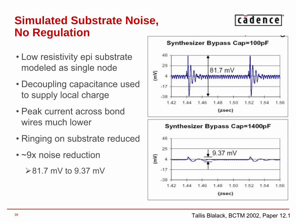
Simulated Substrate Noise, No Regulation
� Low resistivity epi substrate modeled as single node
� Decoupling capacitance used to supply local charge
� Peak current across bond wires much lower
� Ringing on substrate reduced
� ~9x noise reduction
!81.7 mV to 9.37 mV

40 Tallis Blalack, BCTM 2002, Paper 12.1
Simulated Substrate Noise with Regulation
� On-chip voltage regulator added
� Decoupling capacitance at input and output of regulator
� ~100x reduction of noise
!9.37 mV to 0.098 mV
� Minimized inductive connection to substrate

41 Tallis Blalack, BCTM 2002, Paper 12.1
Motorola: CMOS Broadband Tuner
� Synthesizer generates 100 mA switching currents @ 12.5 MHz
� 50 � 860 MHz LNA� 0.35 µm CMOS
� heavily doped bulk
� 5 V supply� 1.5 Watts� 5 mm2
� 48 pin eTQFP
~25% of area to reduce substrate noise ~1000x! 81.7 mV to 98 µV

42 Tallis Blalack, BCTM 2002, Paper 12.1
On-chip RF Isolation Summary
IT DEPENDS on� Technology
� Frequency
� Grounding scheme
� Guard rings
� Package
� Decoupling capacitance
� �
43 Tallis Blalack, BCTM 2002, Paper 12.1
Acknowledgements
The authors would like to thank:
� Takeshita san and Kato san of Sony
� Dave Redmond of Motorola
� Andreia Cathelin and Didier Belot of STMicroelectronics
� Paul van Zeijl of Ericsson
� David Su of Atheros
� Larry Connell of Motorola


![[Curs Android] C07 - Liste (IPW 2011)](https://img.pdfslide.us/doc/110x75/54c7b9194a7959cc278b45dd/curs-android-c07-liste-ipw-2011.jpg)