Embed Size (px)
Citation preview

OFFLINE SINGLE-STAGE ELECTROLYTIC-CAPACITOR-FREE
FLICKER-FREE HIGH POWER LED DRIVER
by
Ya-Jie Qiu
A thesis submitted to the Department of Electrical and Computer Engineering
In conformity with the requirements for
the degree of Doctor of Philosophy
Queen’s University
Kingston, Ontario, Canada
(January, 2017)
Copyright ©Ya-Jie Qiu, 2017
i
Abstract
The use of white LED bulbs has increased exponentially in recent years because of their
low energy consumption, long life time, high luminous efficacy and environmental friendly
features.
The illumination LED bulbs require a controlled constant amount of DC current to emit
a constant light. Therefore, the LED power supplies (LED drivers) determine the lighting
performance. Moreover, it impacts the sales price, daily expense as well as the lifespan of
the lamp.
Conventional single-stage topologies for grid-connected LED drivers with high power
factors (PFs) require large capacitances at the output to limit the low frequency (double
line frequency, i.e. 120 Hz) LED current ripple that causes flicker. Electrolytic capacitors
are commonly used to reduce this low frequency current ripple at the output. LED bulbs
have a long lifespan (>50,000 hours), but the electrolytic capacitor has a short lifespan
(5,000 hours). Therefore, using electrolytic capacitors will significantly reduce the lifespan
of the entire LED lamp.
The basic bipolar ripple cancellation technology has been proposed, using a dc-ac
inverter, to cancel the low-frequency ac ripple in the LED current and thus minimizing the
output capacitance requirement, enabling the use of long-life film capacitors (>50,000
hours).
Furthermore, the improved bipolar ripple cancellation technology with a floating dc-ac
power structure is proposed to accommodate the usage of low-voltage-rating dc-ac inverter
in variable output voltage LED driver applications. The control scheme to achieve both
ripple cancellation and the floating auxiliary capacitor voltage regulation is presented.

ii
In the above two ripple cancellation technologies, the voltage sensing control method
has been used. A new control method, called current sensing control method, is proposed
and implemented to achieve ripple cancellation as well. The method keeps using the
floating dc-ac power structure while provides a simple and low-cost control solution,
compared to the voltage sensing method.
Finally, LLC resonant converter is used as the topology of single-stage high-power LED
driver application to improve the efficiency. The design rule of LLC resonant converter
working in Power-Factor-Correction mode is proposed and the performance is
demonstrated.

For Xiaolin

iii
Acknowledgements
I thank my supervisor, Dr. Yan-Fei Liu, for his guidance, support, encouragement, and
the opportunities he provided in the past five years. He is earnest, diligent, and always
helpful. His guideline for the research, “New and better”, is always endowed me with the
spirit to excel. The knowledge, skills, and the ways of thinking that I learnt from him
empowered me to challenge the future.
I thank my supervisor, Dr. Paresh C. Sen, for his generous support, encouragement, and
mentoring. His dedication to education and his serious attitude to the research showed me
a great example of a respected scholar.
I thank my committee, Dr. Gerry Moschopoulos, Dr. Alireza Bakhshai, Dr. John C.
Cartledge, Dr. Qingguo Li, and Dr. Thomas R. Dean for their valuable suggestions and
help.
I thank the department administrative, especially, Ms. Debra Fraser, Ms. Mary
Gillespie, Ms. Cheryl Wright and Mr. Steve Humphrey for their numerous help in the past
years.
I thank my colleagues, Dr. Zhiyuan Hu, Dr. Peng Fang, Dr. Laili Wang, Dr. Hongliang
Wang, Ms. Xiumei Yue, Mr. Tianshu Liu, Mr. Lei Kou, Mr. Yang Chen, Mr. Wenbo Liu,
Dr. Yan Zhang, Ms. Sarah Burton, Mr. Brian White, Mr. Chris Fiorentino, Mr. Bo Sheng,
and Mr. Andrew Dickson for their friendship, help, and insightful discussions.
My deepest appreciation goes to my wife. I would like to thank my wife, Xiaolin Kang,
for her great support and understanding and the unconditional love to both me and our
lovely son, Yi Nuo Qiu. Her patient and encouragement allow me to ride through the great
challenges that happen in my personal life and my career.

iv
Lastly I would like to thank my parents, Guoqing Deng and Changcong Qiu, and my
brother Yajun Qiu for their interest and support, both emotionally and financially. They
have always supported me in my life choices and this time was no different.

v
Statement of Originality
I hereby certify that all of the work described within this thesis is the original work of the
author. Any published (or unpublished) ideas and/or techniques from the work of others
are fully acknowledged in accordance with the standard referencing practices.
Ya-Jie Qiu
January, 2017

vi
Table of Contents
Abstract ............................................................................................................................................. i
Acknowledgements ......................................................................................................................... iii
Statement of Originality ................................................................................................................... v
List of Figures ................................................................................................................................. xi
List of Tables ................................................................................................................................ xvi
List of Symbols ............................................................................................................................ xvii
Acronym ....................................................................................................................................... xxi
Chapter 1 Introduction ..................................................................................................................... 1
1.1 Background and Motivation .................................................................................................. 1
1.1.1 Luminous Light Technology Development .................................................................... 1
1.1.1.1 Incandescent Lamps ................................................................................................. 1
1.1.1.2 High-Intensity Discharge Lamps ............................................................................. 2
1.1.1.3 Fluorescent Lamps ................................................................................................... 2
1.1.2 High-Brightness Light-Emitting Diode (LED) Light Technology and Its Advantages .. 3
1.2 Basic Functions of High Power Offline LED Drivers ........................................................... 4
1.2.1.1 Constant Output Current Regulation ........................................................................ 4
1.2.1.2 Power Factor Requirements for Offline LED Drivers ............................................. 6
1.3 Conventional Offline High Power LED Driver Circuits and Configurations ........................ 7
1.3.1 Two-Stage LED Driver Configuration ........................................................................... 7
1.3.2 Single-Stage LED Driver Configuration ......................................................................... 9
1.4 Unmatched Life Span Problem between LED Lights and Drivers ........................................ 9
1.4.1 Low Frequency AC Current Ripple from Offline Single-Stage LED Drivers .............. 10
1.4.2 Resulting Light Flicker Issue and IEEE Standards ....................................................... 11
1.4.3 Bulky Output Capacitor Requirement ........................................................................... 13
1.5 Research Objective .............................................................................................................. 14
1.6 Thesis Contribution .............................................................................................................. 15
1.7 Thesis Structure ................................................................................................................... 16
Chapter 2 Literature Review of Electrolytic-capacitor-free and Soft Switching Technologies for
LED Driver .................................................................................................................................... 19
2.1 Introduction .......................................................................................................................... 19
2.2 Research Review On Electrolytic-Capacitor-Free and Flicker-Free LED Drivers
Technologies .............................................................................................................................. 20

vii
2.2.1 Passive Type Offline LED Driver ................................................................................. 20
2.2.2 Active Input Current Shaping Offline LED Driver....................................................... 22
2.2.3 Parallel Ripple Cancellation Offline LED Driver ......................................................... 24
2.2.4 Unipolar Series Ripple Cancellation Offline LED Driver ............................................ 25
2.3 Research Review on Soft Switching Technologies ............................................................. 26
2.3.1 Mechanism of Soft Switching ....................................................................................... 27
2.3.2 Active-Clamp Technology for Flyback Power Factor Correction (PFC) ..................... 30
2.3.3 LLC Resonant Converter .............................................................................................. 31
2.4 Conclusion ........................................................................................................................... 34
Chapter 3 Basic Bipolar Ripple Cancellation LED Driver Concept and its Implementation ........ 36
3.1 Introduction .......................................................................................................................... 36
3.2 Operation Principles of Bipolar Ripple Cancellation Method ............................................. 36
3.2.1 Basic Bipolar Ripple Cancellation Concept .................................................................. 36
3.2.2 Control Strategy for Full Bridge Ripple Cancellation Converter ................................. 39
3.2.3 LED Current Regulation and Power Factor Correction ................................................ 40
3.3 Step by Step Design Procedure for Bipolar Ripple Cancellation Converter........................ 41
3.3.1 Selection of Voltage Rating of the FB RCC Input Capacitor Caux ................................ 41
3.3.2 Selection of the FB RCC Mosfets and Design the Cancellation Stage ......................... 41
3.3.3 Selection of PFC Stage Output Capacitance ................................................................. 42
3.3.4 Design of FB RCC Input Capacitor Caux ....................................................................... 44
3.3.5 Selection of the Auxiliary Winding Turns Ratio .......................................................... 45
3.3.6 CFB and Caux Layout to Suppress the Audible Noise ..................................................... 45
3.4 Analysis of Proposed Bipolar Ripple Cancellation Stage .................................................... 46
3.4.1 Low-Voltage-Rating Components in the Cancellation Stage ....................................... 47
3.4.2 Super Output Capacitance Reduction & Light Flicker Cancellation Ability ................ 47
3.4.3 High Efficiency ............................................................................................................. 48
3.5 Experimental Verification .................................................................................................... 48
3.5.1 Input Voltage and Input Current Waveforms................................................................ 49
3.5.2 LED Current Ripple Cancellation Performance ........................................................... 50
3.5.3 Light Flickering Comparison ........................................................................................ 51
3.5.4 Power Efficiency and Power Factor Performance ........................................................ 53
3.5.5 Prototype Board ............................................................................................................ 56
3.6 Conclusion ........................................................................................................................... 57
Chapter 4 Improved Bipolar Ripple Cancellation Method Using Floating Auxiliary Capacitor ... 59
viii
4.1 Introduction .......................................................................................................................... 59
4.2 Configuration of Improved Bipolar Ripple Cancellation Technology ................................ 60
4.2.1 Basic Bipolar Ripple Cancellation Configuration Review ........................................... 60
4.2.2 Improved Bipolar Ripple Cancellation Configuration Using Floating Auxiliary
Capacitor ................................................................................................................................ 60
4.3 Control Scheme to Achieve Both Ripple Cancellation and Floating Auxiliary Capacitor
Voltage Regulation .................................................................................................................... 63
4.3.1 Under-Cancellation Phenomenon ................................................................................. 64
4.3.2 Combined Control Scheme ........................................................................................... 66
4.3.3 Full Bridge RCC Floating Auxiliary Capacitor Design ................................................ 67
4.4 Analysis of Proposed Floating Auxiliary Capacitor Bipolar Ripple Cancellation Stage ..... 69
4.4.1 Low-Voltage-Stress Power Structure Applicable for both Isolated and Non-Isolated
PFC Topologies ..................................................................................................................... 70
4.4.2 No Overdesigning for Variable-Output-Voltage LED Drivers ..................................... 71
4.4.3 High Efficiency ............................................................................................................. 73
4.4.4 Portable to Existing LED Driver Products to Achieve Electrolytic-capacitor-free and
Flicker-Free ............................................................................................................................ 73
4.5 Experimental Verification .................................................................................................... 75
4.6 Conclusion ........................................................................................................................... 84
Chapter 5 Current Sensing Control Method for Bipolar Ripple Cancellation Technology ........... 85
5.1 Introduction .......................................................................................................................... 85
5.1.1 Background ................................................................................................................... 85
5.2 Current-sensing-based Feedback Control Strategy .............................................................. 89
5.2.1 System Block Diagrams ................................................................................................ 89
5.2.2 Power Structure and Control Circuit ............................................................................. 90
5.3 Advantages of Current-sensing-based Ripple Cancellation Method ................................... 92
5.3.1 Ripple Cancellation Performance ................................................................................. 92
5.3.2 RCC Input Voltage Auto-Tracking to Minimize the RCC Loss at Different Loads ..... 94
5.4 Experimental Verification .................................................................................................... 94
5.4.1 Ripple Cancellation Performance ................................................................................. 95
5.4.2 FB RCC Input Voltage Auto-Tracking Performance .................................................... 97
5.4.3 System Efficiency and Power Factor Correction Performance ..................................... 98
5.4.4 Dimming Performance ................................................................................................ 100
5.5 Conclusion ......................................................................................................................... 101
ix
Chapter 6 Single-stage LED Driver Using LLC Resonant Converter in PFC Mode ................... 102
6.1 Introduction ........................................................................................................................ 102
6.2 Single-Stage PFC Gain Requirement Analysis .................................................................. 103
6.2.1 Single-Stage PFC Operation ....................................................................................... 103
6.2.2 Voltage Gain Requirement.......................................................................................... 104
6.2.3 Instantaneous Output Power Requirement .................................................................. 105
6.2.4 Analysis of PFC Gain Requirement ............................................................................ 105
6.3 LLC Resonant Converter Application in Offline High Power LED Driver ...................... 107
6.3.1 LLC Converter Topology ........................................................................................... 107
6.3.2 LLC Application in Conventional Two-Stage Offline High Power LED Driver ....... 108
6.3.3 AC Equivalent Circuit and Output Voltage Gain for LLC Resonant Tank ................ 109
6.4 LLC Resonant Converter Design Rule for Single-stage PFC ............................................ 112
6.4.1 Switching Frequency Range ....................................................................................... 112
6.4.2 Transformer Turns Ratio Design Rule ........................................................................ 113
6.4.3 LLC Resonant Tank Design Rule ............................................................................... 114
6.4.3.1 Derivation of Gain Expression of LLC Resonant Converter in PFC mode ......... 114
6.4.3.2 Derivation of the Voltage Gain at the Parallel Resonant Frequency of the LLC
Resonant Converter .......................................................................................................... 117
6.4.3.3 Derivation of the LLC Tank Design Rule ............................................................ 118
6.5 LLC Design Rule for LED Driver Applications ................................................................ 120
6.5.1 Offline Wide Input and Output Voltages Single-Stage LED Drivers ......................... 120
6.5.2 Design Rule for LED Driver Application with Wide Input and Output Voltages
Requirements ....................................................................................................................... 120
6.6 LLC PFC Design Example: Single-Stage LLC LED Driver with Wide Input and Output
Voltages ................................................................................................................................... 126
6.6.1 Specifications .............................................................................................................. 126
6.6.2 Transformer Turns Ratio Design ................................................................................ 126
6.6.3 LLC Resonant Tank Gain Requirement ...................................................................... 126
6.6.4 LLC Resonant Tank Design Process .......................................................................... 128
6.6.4.1 Assumption of Resonant Frequencies fp and fr ..................................................... 128
6.6.4.2 Cr Selection .......................................................................................................... 128
6.6.4.3 Lr Selection .......................................................................................................... 130
6.6.4.4 Lm Selection .......................................................................................................... 130
6.6.5 Accurate Switching Frequency Range ........................................................................ 130

x
6.7 Mathematical Verification ................................................................................................. 131
6.7.1 Normalized Gain Curves of the Designed LLC PFC at Typical Loads ...................... 131
6.7.2 LLC PFC design rule verification under Vout=Voutmax .................................................. 133
6.7.3 LLC PFC design rule verification considering the entire output voltage range .......... 134
6.8 Simulation Verification ...................................................................................................... 135
6.8.1 LLC PFC LED Driver Architecture and Simulation Model in PSIM ......................... 135
6.8.2 Power Factor Correction Performance ........................................................................ 138
6.8.3 Ripple Cancellation Performance ............................................................................... 141
6.9 Experimental Verification .................................................................................................. 143
6.9.1 Digital Implementation of LLC PFC Control ............................................................. 143
6.9.2 Power Factor Correction Performance ........................................................................ 147
6.9.3 Soft Switching Performance ....................................................................................... 149
6.9.1 Efficiency Performance............................................................................................... 153
6.9.2 Ripple Cancellation Performance ............................................................................... 155
6.9.3 Prototype Board .......................................................................................................... 156
6.10 Conclusion ....................................................................................................................... 157
Chapter 7 Summary and Future Work ......................................................................................... 159
7.1 Summary ............................................................................................................................ 159
7.2 Future Work ....................................................................................................................... 161
References .................................................................................................................................... 162

xi
List of Figures
Fig. 1.1. Typical Forward Current vs. Forward Voltage, Junction Temperature=85°C For Xlamp
XM-L Easywhite LEDs From Cree [6]............................................................................................ 5
Fig. 1.2. Two-Stage PFC Configuration for LED Applications ..................................................... 8
Fig. 1.3. Single-Stage PFC Configuration for LED Applications ................................................... 9
Fig. 1.4. IEEE standards of max allowable light flicker percentage at different frequency [29] .. 12
Fig. 1.5. Minimal Output Capacitance Requirement vs. Output Voltage Ripple Limitation ........ 13
Fig. 2.1. Valley-Fill-Type Passive LED Driver Solution [33] ...................................................... 21
Fig. 2.2. LC-Series-Resonance-Type Passive LED Driver Solution [34] ..................................... 21
Fig. 2.3. LC3-Type Passive LED Driver Solution [35] ................................................................. 22
Fig. 2.4. Harmonics Injection LED Driver Solution [36, 37] ....................................................... 23
Fig. 2.5. Input power relocation LED Driver Solution 1 [38] ....................................................... 24
Fig. 2.6. Input power relocation LED Driver Solution 2 [39] ....................................................... 24
Fig. 2.7. Parallel Ripple Cancellation LED Driver Solution [40-43] ............................................ 25
Fig. 2.8. Unipolar Series Ripple Cancellation LED Driver Solution ............................................ 26
Fig. 2.9. Full-Bridge Inverter Topology ....................................................................................... 27
Fig. 2.10. ZCS Condition and Device Waveforms ....................................................................... 28
Fig. 2.11. ZVS Condition and Device Waveforms ....................................................................... 29
Fig. 2.12. Basic Single-stage Flyback Power Factor Correction Topology .................................. 30
Fig. 2.13. Active Clamp Single-stage Flyback Power Factor Correction Topology .................... 31
Fig. 2.14. DC-DC LLC Resonant Converter Topology. ............................................................... 32
Fig. 2.15. Voltage Gain Plot of LLC Resonant Converter ............................................................ 33
Fig. 3.1. Bipolar Ripple Cancellation LED Driver Concept: (a) Circuit Block Diagram (b) The
Key Waveforms ............................................................................................................................. 37
Fig. 3.2. Electrolytic-Capacitor-Free LED Driver Architecture with Full Bridge Ripple
Cancellation Converter .................................................................................................................. 39
Fig. 3.3. Control Block Diagram of Bipolar Ripple Cancellation. ............................................... 40
Fig. 3.4. LED Current Regulation and Power Factor Correction .................................................. 41
Fig. 3.5. PFC Output Capacitance vs. PFC Output Pk-to-Pk Voltage Ripple with LED Current of
0.7A................................................................................................................................................ 43
Fig. 3.6. Operation Modes of Bipolar Ripple Cancellation Converter (a) Stage Prototype (b)
Operation Modes ............................................................................................................................ 46

xii
Fig. 3.7. Input Current and Output Voltage of the Proposed LED Driver, When Vin=110Vac, VLED
≈150V, ILED=0.7A, Po=100W ....................................................................................................... 49
Fig. 3.8. Ripple Cancellation Performance of the Proposed LED Driver, When Vin=110 Vac, VLED
≈150V, ILED=0.7A, Po=100W. ...................................................................................................... 51
Fig. 3.9. Light Flickering Reduction Performance Comparison, When Vin=110Vac, VLED≈150V,
ILED=0.7A, Po=100W. .................................................................................................................... 53
Fig. 3.10. Performance of Bipolar Ripple Cancellation LED Driver When Cmain=44µf, VLED≈
150V, ILED=0.7A, Po=100W. .......................................................................................................... 54
Fig. 3.11. Bipolar RCC Loss Performance, When Cmain=44µf, VLED≈150V, ILED=0.7A,
Po=100W. ....................................................................................................................................... 55
Fig. 3.12. Harmonic Performance at Nominal Input Voltage ....................................................... 56
Fig. 3.13. Prototype Photos of Bipolar Ripple Cancellation Electrolytic-Capacitor-Free LED
Driver. ............................................................................................................................................ 57
Fig. 4.1. Circuit Block Diagram of the Basic Bipolar Ripple Cancellation LED Driver. ............. 60
Fig. 4.2. Floating Auxiliary Capacitor Bipolar Ripple Cancellation Principle: (a) Circuit Block
Diagram (b) The Key Waveforms ................................................................................................. 62
Fig. 4.3. Implementation of Floating Auxiliary Capacitor Full-Bridge Bipolar Ripple
Cancellation LED Driver Architecture. ......................................................................................... 63
Fig. 4.4. Combined Control Scheme of Floating Auxiliary Capacitor Bipolar Ripple Cancellation
Control Strategy. ............................................................................................................................ 64
Fig. 4.5. Under-cancellation Phenomenon Analysis. .................................................................... 65
Fig. 4.6. Floating Auxiliary Capacitor Bipolar Ripple Cancellation Converter Operation. (a)
Stage Prototype. (b) Operation Modes ........................................................................................... 70
Fig. 4.7. Implementation of Improved Bipolar Ripple Cancellation Technology on Primary-side
Regulated LED Driver ................................................................................................................... 74
Fig. 4.8. Key Experimental Waveforms of Floating Auxiliary Capacitor Bipolar Ripple
Cancellation, When Vin=110Vac, VLED≈150V, ILED=0.7A, PO=100W ......................................... 77
Fig. 4.9. Cancellation Performance of the Floating Auxiliary Capacitor RCC LED Driver, When
Vin=110Vac, VLED≈150V, ILED=0.7A, PO=100W. ......................................................................... 78
Fig. 4.10. Input Current and Output Voltage of the Floating Auxiliary Capacitor Bipolar RCC
LED driver, when Vin=110Vac, VLED≈150V, ILED=0.7A, PO=100W ............................................ 79

xiii
Fig. 4.11. Power Factor Comparison of The LED Driver With Floating auxiliary capacitor RCC
and Winding-connected RCC and At Full Load, When Cmain=56 µf, VLED≈150V, ILED=0.7A,
Po=100W. ....................................................................................................................................... 80
Fig. 4.12. Harmonic Performance of Floating Auxiliary Capacitor RCC LED Driver at Nominal
Input Voltage ................................................................................................................................. 80
Fig. 4.13. Power Conversion Efficiency Comparison of LED Driver With Floating Auxiliary
Capacitor RCC and Winding-connected RCC and At Full Load, When Cmain=56 µf, VLED≈150V,
ILED=0.7A, Po=100W. .................................................................................................................... 81
Fig. 4.14. Floating auxiliary capacitor RCC stage loss in LED driver when VLED≈150V,
ILED=0.7A, Po=100W. .................................................................................................................... 82
Fig. 4.15. Dimming Performance of the LED Driver With Floating Capcitor RCC, When
Cmain=56µf, VLED≈150V.................................................................................................................. 83
Fig. 5.1. The Floating Auxiliary Capacitor Bipolar Ripple Cancellation LED Driver Method .... 87
Fig. 5.2. The Voltage-Ripple-Sensing-Based Control Strategy for Bipolar Ripple Cancellation. 88
Fig. 5.3. Current-sensing-based Control Strategy for Bipolar Ripple Cancellation ..................... 89
Fig. 5.4. The Flicker-Free LED Driver With Full-Bridge Bipolar RCC[67]. ............................... 91
Fig. 5.5. Implementation of Current-sensing-based Control Method. .......................................... 91
Fig. 5.6. Equivalent Circuit Model of LED String Load .............................................................. 93
Fig. 5.7. Key Waveforms of the Proposed Current-sensing-based Ripple Cancellation Method,
When Vin=110Vac, ILED=0.7A ........................................................................................................ 96
Fig. 5.8. FB RCC Input Voltage Auto-Tracking Performance, When Vin=110Vac ...................... 97
Fig. 5.9. Input Current and Output Voltage of the Proposed LED Driver, When Vin=110Vac and
220Vac, VLED≈150V, ILED=0.7A ................................................................................................... 98
Fig. 5.10. Performance of the Floating Auxiliary Capacitor Bipolar RCC LED Driver with
Current-sensing-based Control Method At Full Load, When Cmain=56 µf, VLED≈150V, ILED=0.7A.
....................................................................................................................................................... 99
Fig. 5.11. Full Bridge Converter Loss in Floating auxiliary capacitor Bipolar RCC LED Driver,
When VLED≈150V, ILED=0.7A, Po=100W. .................................................................................. 100
Fig. 5.12. Dimming Performance of the LED Driver Under Current-sensing-based Ripple
Cancellation Method, When Cmain=56µf, VLED≈150V. ............................................................... 101
Fig. 6.1. Single-stage Power Factor Correction Circuit .............................................................. 104
Fig. 6.2. Gain Requirement of Power Factor Correction Under Different Phase Angle of Line
Voltage ......................................................................................................................................... 106

xiv
Fig. 6.3. Schematic of Half-Bridge LLC Resonant Converter. ................................................... 107
Fig. 6.4. Typical LLC Resonant Converter Application in Offline Two-Stage LED Driver. ..... 108
Fig. 6.5. Proposed Single-Stage LLC Resonant AC-DC LED Driver. ....................................... 109
Fig. 6.6. AC Equivalent Circuit for LLC Resonant Converter ................................................... 109
Fig. 6.7. Voltage Gain Plot of LLC Resonant Converter ............................................................ 111
Fig. 6.8. AC Equivalent Circuit for LLC Resonant Converter in PFC Mode ............................. 115
Fig. 6.9. Gain Requirement Under Different Inputs & Outputs.................................................. 127
Fig. 6.10. VCr Changing Curve at Minimum Frequency ............................................................. 129
Fig. 6.11. Normalized Gain Plot of the Designed LLC Resonant Converter at heaviest load
pO(θ=π/2)=2PO ............................................................................................................................. 132
Fig. 6.12. Normalized Gain Plot of the Designed LLC Resonant Converter at other typical loads
..................................................................................................................................................... 132
Fig. 6.13. Gain Requirement and Gain Curve of the Designed LLC Resonant Converter
Considering the Highest Output Voltage (Vout=Voutmax) ............................................................... 133
Fig. 6.14. Designed LLC Resonant Converter Gain & PFC Gain Requirement in 3D Surface Plot
Considering the Wide Output Voltage (Voutmin<Vout<Vout
max) ....................................................... 134
Fig. 6.15. Proposed Single-Stage LLC PFC LED Driver Architecture with Full-Bridge Ripple
Cancellation Converter ................................................................................................................ 135
Fig. 6.16. Proposed Single-Stage LLC PFC LED Driver Simulation Model in PSIM. .............. 137
Fig. 6.17. Simulation Results of LLC PFC in Case 1 (Resonant Tank Parameters: Lm=103µH
Lr=20µH Cr=20.4nF) ................................................................................................................... 139
Fig. 6.18. Simulation Results of LLC PFC in Case 2 (Resonant Tank Parameters: Lm=103µH
Lr=20µH Cr=20.4nF) ................................................................................................................... 140
Fig. 6.19. Bipolar Ripple Cancellation Performance in Simulation in Two Typical Cases when
Iout=ILED=4A (Resonant Tank Parameters: Lm=103µH Lr=20µH Cr=20.4nF) ............................. 142
Fig. 6.20. The Implementation of the Proposed Single-Stage LLC Resonant LED Driver. ....... 144
Fig. 6.21. Input Voltage, Input Current and Output Voltage of the Designed Single-stage LLC
LED Driver .................................................................................................................................. 147
Fig. 6.22. Power Factor Performance of LLC PFC LED Driver When VLED≈40~60V, ILED=4A.
..................................................................................................................................................... 148
Fig. 6.23. Soft Switching Performance of the LLC PFC Stage on Primary Side at Different Phase
Angle, When Vin=180Vac, VLED≈60V, ILED=4A, PO=240W....................................................... 150
Fig. 6.24. Soft Switching Performance of the LLC PFC Stage on Secondary Side at Different
Phase Angle, When Vin=180Vac, VLED≈60V, ILED=4A, PO=240W ............................................ 152

xv
Fig. 6.25. LLC PFC LED Driver Efficiency Performance under Different Input Voltage ......... 154
Fig. 6.26. Key Waveforms of Bipolar Ripple Cancellation in the Proposed LLC PFC LED Driver
..................................................................................................................................................... 156
Fig. 6.27. 240W Single-Stage LLC PFC LED Driver Prototype Photos .................................... 157

xvi
List of Tables
Table 1.1. High power lighting technology comparison[5] ............................................................ 4
Table 1.2. Harmonics limits for lighting equipment from IEC 61000-3-2 Class C Standard ......... 7
Table 1.3. Specifications of offline single-stage high-power LED driver .................................... 13
Table 3.1. Specifications of bipolar ripple cancellation LED driver ............................................ 43
Table 3.2. Bipolar RCC input capacitor Caux design parameters .................................................. 45
Table 3.3. Bipolar ripple cancellation LED driver prototype parameters ..................................... 49
Table 4.1. Floating auxiliary capacitor bipolar ripple cancellation LED driver prototype
Parameters ...................................................................................................................................... 75
Table 4.2. Bipolar RCC floating auxiliary capacitor Caux design parameters ............................... 76
Table 5.1. Current sensing bipolar ripple cancellation LED driver prototype parameters ........... 95
Table 6.1. Single-stage LLC LED driver specifications ............................................................. 126
Table 6.2. LLC tank gain requirement at the parallel resonant frequency (fp) ............................ 127
Table 6.3. Designed LLC resonant tank parameters ................................................................... 130
Table 6.4. Key parameters in single-stage LLC LED driver simulation model.......................... 138
Table 6.5. Key circuit components and parameters in LLC LED driver prototype .................... 146
Table 6.6. LED voltage adjustor setting ..................................................................................... 157

xvii
List of Symbols
Rdyn Dynamic resistance of each LED chip.
VF LED chip forward voltage.
IF LED chip forward current.
oV Peak to peak value of the LED voltage ripple at double line frequency
Radian frequency of the line voltage
inP The average input power
f The frequency of the input line voltage
_out ledC Output capacitor of the LED driver
oI Output current
vaux Auxiliary capacitor voltage in ripple cancellation LED driver solution
Vaux Average input voltage of full bridge bipolar ripple cancellation converter
ωr LLC converter radian series resonant frequency
ωs Radian switching frequency of LLC converter
fn The normalized switching frequency of LLC converter
Q The quality factor
K The inductance ratio in LLC resonant converter
Lr The series resonant inductor in LLC resonant converter
Cr The series resonant capacitor in LLC resonant converter
RL Load resistance of LLC resonant converter
Cmain Main stage (PFC stage) output capacitor
Daux The secondary side rectifier diode of auxiliary stage
CFB Full-Bridge bipolar ripple cancellation converter output capacitor
VLED Voltage across the LED load
ILED Current through the LED load
vmain Main stage (PFC stage) output voltage
vFB Full-Bridge bipolar ripple cancellation converter output voltage
VDC The DC component of the PFC output voltage
vripple The double line frequency AC component of PFC output voltage
Caux Input capacitor of full bridge bipolar ripple cancellation converter

xviii
Ns2 The second secondary side transformer winding
Ns1 The first secondary side transformer winding
Vmain_ripple The double line frequency ripple component in the main output voltage
Vripple Peak to peak double line frequency voltage ripple value
Vmain_pk The maximum voltage stress on the PFC stage output capacitor
fsw Switching frequency of the FB RCC converter
VCaux_peak The peak voltage value of the input capacitor of FB RCC converter
VCaux_valley The valley voltage value of the input capacitor of FB RCC converter
fline The line voltage frequency
Tline The line voltage cycle period
Qmain The main switch in the active clamp Flyback PFC converter
Qaux The auxiliary switch in the active clamp Flyback PFC converter
Dmain The main secondary side diode of the Flyback PFC converter
Lm Magnetizing inductance
VCaux_ripple The allowed input voltage ripple value
Llek Leakage inductance
Lext External leakage inductor
Cclamp Active clamp capacitor 250V Film Caps)
Clump Lumped capacitance
Q1~Q4 Full bridge switches in bipolar ripple cancellation converter
vFB_atten Scaled FB RCC output voltage
Vcaux_ref The reference for the input voltage of FB RCC
vspwm1 Part of the spwm control signal contributed by the ripple cancellation loop
vspwm2 Part of the spwm control signal contributed by the rcc loss offset loop
vspwm_sum Spwm control signal for the FB RCC
iin AC input current
Ilit_flick_FFT FFT of reflected light flickering in voltage
vlit_flick AC coupled reflected light flickering in voltage
VCaux_avg DC average voltage of FB RCC
Tsw The switching period of RCC stage
D Duty cycle of the driving signals for full bridge switches
M The modulation index of SPWM
Qdischarge The discharge of Caux in each switching cycle

xix
Qdischarge_sum The sum of discharge of Caux during n switching cycle
VFB,max Component stress of full bridge switches in bipolar RCC
Vcomp_p Primary side compensation signal for LED current regulation
Vcomp_s Secondary side compensation signal for LED current regulation
Iref Output current reference
Ierr Ouput current error signal
vrip_err Ripple voltage error signal
Vcomp_ctrl FB RCC compensation control signal
Vmain_rip Double line frequency component in main stage output voltage
Vpfc_ctrl PFC stage control signal
irip Double line frequency component in LED current
Irip_err Double line frequency component error signal in LED current
Irip_ref Double line frequency component reference
Vbias Bias voltage
Rsense LED current sensing resistor
SH, SL High side and low side switches in half bridge LLC resonant converter
Co Output capacitor
MLLC_total (θ) The total gain of LLC converter
Greq(θ) The gain requirement for the PFC
n The turns ratio of the transformer
MLLC(fs) The gain of the resonant tank of the LLC converter
fr LLC converter series resonant frequency
fp LLC converter parallel resonant frequency
p(θ) Instantaneous input power of PFC converter
Rac LLC resonant converter the equivalent load resistance in PFC mode
Qpfc LLC resonant converter quality factor in PFC mode
( )2
reqG
The gain requirement of single-stage PFC at θ=π/2
( , )2
LLC pM f
The obtainable parallel resonant frequency output voltage gain of LLC resonant
tank at θ=π/2
fpeak The peak voltage gain switching frequency
Voutmin Minimum DC output voltage
xx
Vinmax Maximum AC input voltage (RMS value)
Vin_RMSmin Minimum AC input voltage (RMS value)
Vin_RMSmax Maximum DC output voltage
_ ( )req drivG λ-related gain requirement of variable output range LLC LED driver
Greq_driv The voltage gain requirement for an LLC LED driver
ndriv The transformer turns ratio of the designed half bridge LLC LED driver

xxi
Acronym
LED Light-emitting diode
CFL Compact fluorescent light
PFC Power Factor Correction
Aux Auxiliary
Max Maximum
Min Minimum
ZCS Zero current switching
ZVS Zero voltage switching
Pk-to-pk Peak to peak
AC Alternating current
DC Direct current
RMS root mean square
SSL Solid state lighting
HID High intensity discharge
HPS High pressure sodium
PF Power factor
Eff Efficiency
THD Total harmonic distortion
EMI Electromagnetic interference
SEPIC Single-ended primary inductance converter
PI Proportional–integral
FB Full bridge
SW Switching
Avg Average
RCC Ripple cancellation converter
SPWM Sinusoidal Pulse Width Modulation
CCM Continuous current mode

1
Chapter 1
Introduction
1.1 Background and Motivation
LED (light-emitting diode) is also referred as solid state lighting (SSL) because this technology
is based on solid state physics. It has been over more than 50 years since LED was first introduced
as a practical light source in 1962 by Nick Holonyak at General Electric. In 1993, Shuji Nkamura,
the engineer at Nichia, invented the first high-brightness blue LED, making it possible to generate
a pure white light from LED by combining the blue light with the other two colors: red and green.
Another mainstream method to generate white light is to coat the blue LED emitter with a lasing
medium (Y3Al5O12:Ce, a phosphor material layer) to produce a yellow light. The combination of
that yellow light with the remaining blue light also appears white to the eye [1]. In 2014, Shuji
Nakamura shared the Nobel Prize in Physics together with Prof. Isamu Akasaki and Prof.
Hiroshima Amano for this epoch-making invention. Now LED represents the most
environmentally friendly way of lighting for use in commercial, hospitality, institutional and
residential applications, as they contain no hazardous materials, consume less energy and last
longer than conventional light sources [2, 3].
1.1.1 Luminous Light Technology Development
Before the LED technology went into the market, three other light technologies appeared in
history. They are incandescent lamps, high intensity discharge (HID) lamps and fluorescent lamps.
1.1.1.1 Incandescent Lamps
Incandescent technology produces light by heating up a metal filament enclosed within the
lamp’s glass. Incandescent Lamps are “standard” electric light bulbs that were invented more than

2
125 years ago by Thomas Edison. They have the lowest initial cost, good color rendering and but
are notoriously inefficient. They typically have short life spans and use significantly more watts
than CFLs and halogen lamps do to produce the same lumens, or light output.
1.1.1.2 High-Intensity Discharge Lamps
High-intensity discharge lamp is the second generation of light for outdoor lighting which tries
to provide the greatest amount of photonic illumination for the least consumption of electricity. It
includes Mercury Vapor lamps (outdated and almost extinct) and High Pressure Sodium lamps
(HPS).
Mercury Vapor Lamps were introduced in 1948. It was deemed a major improvement over the
incandescent light bulb, and provided much brighter than incandescent or fluorescent lights.
However, it has the disadvantages that a significant portion of their light output is ultraviolet, and
they get steadily dimmer and dimmer with age while using the same amount of energy.
High Pressure Sodium (HPS) lamps were introduced in around 1970 and are one of the more
popular outdoor lighting options, the most efficient light source when compared to mercury vapour
and metal halide lamps (on a ‘lumen/ watt’ scale). The disadvantage is that they produce narrow
spectrum light mostly a sickly yellow in colour. These lights have a very low colour rendering
index and do not reproduce colours faithfully.
1.1.1.3 Fluorescent Lamps
The fluorescent lamp first became common in the late 1930s. They are much more efficient
than incandescent lamps, but less efficient than High Pressure Sodium. The major problem with
standard fluorescent lamps for outdoor lighting is that they are large, and produce a diffused non-
directional light. They are also susceptible to low voltage failure, prone to breakage of glass parts
and contain harmful mercury. Therefore, the fixtures needed to be large, and could not be mounted

3
more than 20–30 feet above the pavement if they were to produce an acceptable light level.
Fluorescent lamps quickly fell out of favour for main street lighting, but remained very popular
for parking lot and outside building illumination for roadside establishments.
1.1.2 High-Brightness Light-Emitting Diode (LED) Light Technology and Its Advantages
High-brightness LEDs are also called “illumination-grade” LEDs, which are high-output
devices and can be driven at high current of hundreds of milliampere to several Ampere to produce
high intensity light. They have a lot of applications in the public area lighting such as Traffic signs,
Tunnel lighting and Monument lighting as well. With the development of manufactory technology,
high-brightness LED becomes more accessible than several tens of years before.
In Table 1.1, a detailed comparison is made among the different high power outdoor lighting
technologies. The LED lighting technology is not only energy-saving but also environmentally
friendly. In 2008, Cree Inc. released XLAMP MC-E LEDs that can operate at 700mA with
maximum lumen flux 571 lm (www.cree.com). The typical application of high power LED lights
is street lights. Compared to traditional street lights, which typically have a reflector on the back
side such as high-pressure sodium lamps, LED street lights have a lens on the LED panel, which
is designed to cast its light in a rectangular pattern. In this case, most luminance of the LED light
is saved and produces no light pollution in the air and surrounding environment. Therefore, more
and more governments and metropolitans choose LEDs to illuminate the streets.
About nineteen percent of the world’s electricity is used for lighting [4], the significant
economic benefit and promising future applications of high power LED light have stimulated my
initial interest in LED lighting technology research.

4
Table 1.1. High power lighting technology comparison[5]
Light
technology
Life time
(hours)
Lumens
per watt
Color rendering
index
Ignition
time considerations
Incandescent
light
1,000 -
5,000 11 - 15 40 instant
very inefficient, short
life time
Mercury
vapor light
12,000 -
24,000 13 - 48 15 - 55
up to 15
min
very inefficient,
ultraviolet radiation,
contains mercury
Metal halide
light
10,000 -
15,000 60 - 100 80
up to 15
min
high maintenance UV
radiation, contains
mercury and lead,
risk of bursting at the
end of life
Fluorescent
light
10,000 -
20,000 60 - 100 70 - 90
up to 15
min
UV radiation,
contains mercury,
prone to glass
breaking, diffused
non-directional light
Compact
fluorescent
light
12,000 -
20,000 50 - 72 85
up to 15
min
low life / burnout,
dimmer in cold
weather (failure to
start), contains
mercury
LED light 50,000 -
100,000 70 - 150 85 - 90 instant
relatively higher
initial cost
1.2 Basic Functions of High Power Offline LED Drivers
1.2.1.1 Constant Output Current Regulation
Fig. 1.1 provides the diode-like electrical characteristics of a typical LED chip (XLamp XM-L
EasyWhite LEDs from Cree)[6]. It is noticed that when the LED operates at its typical operating
current Ityp (in this case 1250mA), the V-I current slope is very steep, meaning the dynamic
resistance of the LED is very small, compared with low forward current condition. Dynamic

5
resistance Rdyn has been defined in equation (1-1). When the LED chip is driven at output current
Iout. Typical LEDs’ dynamic resistances are varying from Ohms to tens of milliohms.
F out
Fdyn
F I I
VR
I
(1-1)
Therefore, even a small change of the LED driver output voltage to the LED will create a big
change on the LED current. For instance, when the VF is increased from 6.1V to 6.2V (about 1.6%),
the IF goes up from 1220mA to 1438mA (about 15%), the dynamic resistance is 0.46Ω. This
changing current will result in significant luminous fluctuation (flicker) due to the almost linear
relationship between operating current and luminous output of LED chips. So an LED diver is
preferably a constant current source which drives the LED in the operating point, instead of a
voltage source, meaning constant output current regulation is the most fundamental requirement
for any LED driver.
Fig. 1.1. Typical Forward Current vs. Forward Voltage, Junction Temperature=85°C For Xlamp XM-L Easywhite
LEDs From Cree [6]

6
1.2.1.2 Power Factor Requirements for Offline LED Drivers
In general, LED drivers are classified into two families regardless of the operating power level:
DC/DC LED drivers and AC/DC LED drivers. DC/DC LED drivers accept the power from DC
sources and output the constant DC power to the LED bulbs. The typical applications include
automotive off-road light, aircraft lights and LED-array-based projection displays. AC/DC LED
drivers convert the AC power from the grid into the DC power to drive the LED bulbs, so AC/DC
LED drivers are also called offline LED drivers. According to the operating power level, offline
LED driver falls into three different kinds including low power offline LED driver (under 25W),
medium power offline LED driver (25W ~ 100W) and high power offline LED driver (over 100W).
The typical low power offline LED driver applications include indoor decorative lamps, down
lights, under cabinet lights and desk lamps, while the typical medium power and high power offline
LED driver applications include the street lights, high bay lights and parking lot lights.
Unlike the output current regulation feature that is the requirement for all the LED drivers due
to the diode-like electrical characteristics, power factor requirement is typically required for the
medium(25W<Pout<100W) and high power (Pout >100W) level offline LED drivers.
The PF and THD guidelines for lighting have been proposed by Energy Star (US) and IEC (EU).
Energy Star program directives require power factor (PF) for solid stage lighting luminaires with
the power level higher than 5W to be greater than 0.7 for residential applications and 0.9 for
commercial applications [19]. IEC 61000-3-2 Class C standard gives the input current harmonics
standard for lighting equipment for LED power over 25 W, requiring the maximum THDi below
30% .The limits on every harmonics order are listed in Table 1.2.

7
Table 1.2. Harmonics limits for lighting equipment from IEC 61000-3-2 Class C Standard
Harmonics
[n]
Class C
[% of fundamental]
2 2%
3 30×λ%
5 10%
7 7%
9 5%
11 3%
13 3%
15<n<39 3% λ — power factor of the circuit
It is in the manufactories’ interest to have a good power (typically >0.95) for high power LED
driver applications such as street light, flood light, high bay light. Therefore, it is necessary to
guarantee high input power factor (PF) and low total harmonic distortion (THD) for the offline
LED driver with the power level over 25W.
1.3 Conventional Offline High Power LED Driver Circuits and Configurations
As an important branch of LED drivers study, offline high-power LED drivers (Po>100W) are
commonly used in outdoor lighting applications such as street lights, parking lot lights and high
bay industrial lights.
Conventional offline LED drivers can be classified into two types according to their
configurations: single-stage LED driver and two-stage LED driver. They are separately used in
markets according to the power level and the application requirements.
1.3.1 Two-Stage LED Driver Configuration
Two-stage topology is the most widely used one to drive the LED loads over intermedium
power level (over 25W).
Fig. 1.2 shows the configuration of two-stage LED drivers. Typically, there are four elements
in the configuration, including electromagnetic interference (EMI) filter, rectifier, PFC converter

8
stage and DC-DC converter stage. EMI filter and rectifier that provide electromagnetic noise
suppression and AC voltage to DC voltage rectification are the preliminary stages for the later
active conversion, while the other two elements, PFC stage and DC-DC converter stage, are the
functional stages with active controls in the two-stage configuration [7, 8]. The PFC stage is
normally a non-isolated topology such as Boost converter or Buck converter. They take the roll of
power factor correction (PFC) to ensure the highest power factor as well as the lowest THD. The
DC-DC converter stage is an isolated stage, such as Flyback converter, LLC resonant converter or
Asymmetrical Half-Bridge[9]. It is the key component in the LED driver that generates constant
current to the LED lamp. The common solution of two-stage LED driver is Boost PFC+Flyback.
If the power level goes high up to 150W, the solution of Boost+LLC topologies become more
popular as LLC is better at high power conversion with high efficiency.
PFC Stage DC-DC Stage
Vbus
Cbvo
+
_
LED
Lamp
EMI filter Rectifier
+
_
Line
voltage
Fig. 1.2. Two-Stage PFC Configuration for LED Applications
Although the two-stage AC-DC LED driver can drive LEDs in good operating performance, it
has the shortcoming such as having too many components, large size, low efficiency and relatively
high cost [10]. Compared to the single-stage LED driver, the two-stage topology is suffering from
the low power conversion efficiency since the power is converted twice through this cascaded
configuration.

9
1.3.2 Single-Stage LED Driver Configuration
Considering the drawbacks of the two-stage LED driver configuration, substantial research has
been focused on single-stage PFC configurations in LED applications. It integrates the PFC stage
and DC/DC stage into one circuit, leading to simple topology at low cost. For single-phase LED
drivers that utilize an AC input source, power factor correction (PFC) control must be imposed in
the driver to achieve a high power factor to meet relevant harmonic standards, e.g., ICE61000-3-
2[11]. State-of-the-art LED drivers using the single-stage PFC topology have been published
including the Flyback [12, 13], single-ended primary inductance converter (SEPIC) [8, 14-16],
buck-boost [17, 18], resonance-assisted buck [19], and buck [20], [21] converter. The
configuration of single-stage LED driver configuration is shown in Fig. 1.3. It is noticed that
single-stage LED driver enjoys the feature of low component count, small size and high efficiency
since there is only one stage and all the power is converted only once before it drives the LED
lamp. However, the conventional single-stage LED driver configuration suffers from the short life
span and the flicker problem.
Line
voltage
DC-DC
Converter
Vo
+
_
LED
Lamp
EMI filter Rectifier
Fig. 1.3. Single-Stage PFC Configuration for LED Applications
1.4 Unmatched Life Span Problem between LED Lights and Drivers
Although the LED lights normally have the typical energetic life span over 50,000 hours, the
average life expectancy of a conventional off-line single-stage LED driver is usually less than
5,000 hours. In fact, it is the short life span of the components in LED driver that shorten the life
span of the whole LED lamp products.

10
In the traditional single-stage LED driver configurations, bulky capacitors are applied at the
output of the LED driver to alleviate the AC output current ripple at double line frequency. These
capacitors are usually electrolytic as they must be of large capacitance per unit volume while at
low price. However, electrolytic capacitor is not recommended in LED driver as it suffers from
the deadly drawback of relatively short operating life [22] (<5,000 hours), compared to the lifetime
of LEDs (>50,000 hours [23]). The electrolytic capacitor life is a function of temperature. As a
rule of thumb, its life reduces by half for each 10 °C higher operating temperature. Therefore, the
problem becomes more serious for the outdoor LED applications such as street light working in
the extremely harsh environment.
Long life film capacitor is the ideal substitute with quite long life span (>50,000 hours [24]) in
the extreme environment, but it suffered from the high cost as well as the big volume.
1.4.1 Low Frequency AC Current Ripple from Offline Single-Stage LED Drivers
AC-DC converter is applied between utility grid and LED lamps in order to provide constant
power for LED bulbs and to achieve power factor correction (PFC) function simultaneously. When
PFC function is realized, input power is pulsating while constant output power is required. Since
there is always an instantaneous input and output power difference in a half line cycle, a low
frequency voltage ripple presents on LED Driver output capacitor due to the charging and
discharging action at twice of the line frequency [25]. The energy difference in a half line cycle is
buffered by output capacitor. Because of the low internal dynamic resister characteristic of LED
load, even a low ripple voltage will produce a significant in phase LED ripple current at double
line frequency (e.g. 120Hz) as well. This low frequency LED ripple current will be represented as
flicker in LED light. Assume the unity power factor is achieved, the relationship is shown in the
(1-2).
11
_ _2
in oo
out led o out led
P IV
C V f C
(1-2)
The parameters in (1-2) are as follows: oV is the peak to peak value of the voltage ripple at the
output of the LED driver; is the radian frequency of the input line voltage; inP is the input power;
f is the frequency of the line voltage; _out ledC is the output capacitor of the driver; oI is the output
current.
1.4.2 Resulting Light Flicker Issue and IEEE Standards
Since the line frequency is fixed, the amplitude of the double line frequency voltage only
depends on the average output current as well as the output capacitor. This current ripple will cause
flicker in LED light, which refers to quick, repeated changes in light intensity. In this case, light
flicker is caused when the voltage supplied to a light source (LED bulbs) fluctuates.
According to the public report created by the IEEE standards working group, IEEE PAR1789,
"Recommending practices for modulating current in High Brightness LEDs for mitigating health
risks to viewers", the flicker provided in LED lighting at double line frequency may induce
biological human response [26]. The risks could include seizures and less specific neurological
symptoms including malaise and headache. Seizures can be triggered by flicker in individuals with
no previous history or diagnosis of epilepsy [27-29].
The ENERGY STAR requirement for lamps (Light Bulbs) has specified that the highest percent
flicker and highest flicker index must be reported although it does not specify a maximum
acceptable limit for either [30]. The Alliance for Solid-State Illumination System and Technologies
(ASSIST) defines flicker acceptability criteria based on their testing [31]. According to the
ASSIST criteria, at 100 Hz, percent flicker greater than 20 percent is unacceptable, and at 120 Hz,
percent flicker greater than 30 percent is unacceptable[31]. In January 2015, IEEE PAR1789

12
committee and IEEE board have passed IEEE STD 1789-2015 [32], “IEEE Recommended
Practices for Modulating Current in High-Brightness LEDs for Mitigating Health Risks to
Viewers”, where the stricter allowable flicker percentage is specified. According to the
“Recommended Practice”, and the max allowable flicker percentage at different frequency
(>100Hz) is calculated by multiplying the frequency by 0.08 and round up to the nearest whole
number, as shown in Fig. 1.4. At 120 Hz frequency, max allowable flicker percentage is 10% [29,
32].
Fig. 1.4. IEEE standards of max allowable light flicker percentage at different frequency [29]

13
1.4.3 Bulky Output Capacitor Requirement
According to (1-2), the easiest solution to mitigate the ripple is to apply large capacitors (they
are usually electrolytic) as energy storage devices to buffer the pulsating power difference between
the input and output.
Table 1.3. Specifications of offline single-stage high-power LED driver
Vin(Vac) Vout(Vdc) Iout(A) Po(W) f(Hz)
90-260 150 0.7 100 60
Given the LED driver parameters shown in the Table 1.3, the relationship between the output
voltage ripple amplitude of LED driver and the output storage capacitance is plotted in Fig. 1.5
according to (1-2).
Fig. 1.5. Minimal Output Capacitance Requirement vs. Output Voltage Ripple Limitation
According to the updated flicker acceptability criteria defined by IEEE board [29], the
amplitude of flicker at the double line frequency (120Hz) has to be less than 10 percent.
Considering the linear relationship between the driving current and the output lumens from the
LED lamp, the double line frequency current ripple has to be reduced to be mitigated to 10% also,
as shown in (1-3).
0 0.5 1 1.5 2 2.5 3 3.5 4 4.5 50
0.002
0.004
0.006
0.008
0.01
Unit: V
Un
it:
F
Cout Vout( )
Vout

14
_
10%LED ripple ripple
LED string LED
I V
I r I
(1-3)
For Xlamp XM-L Easywhite LEDs From Cree [6], the dynamic resistance is 0.46Ω for each
chips. The LED voltage is chosen as 150V for the 100W high power LED application to limit the
LED current less than 0.7A, resulting the low double line frequency voltage ripple peak value less
than 30V, according to (1-2). In order to obtain 150V LED voltage, 27 pieces of chips are
connected, results the total dynamic resistance of 12.4Ω. By substitute rstring value into (1-3), the
maximum allowable voltage ripple is 0.9V.
0.9rippleV V (1-4)
According to (1-2), in order to mitigate the double line frequency voltage ripple under 0.9V
volt, a large output capacitor of 2063 F is needed at minimum, which is not a practical number
for the film capacitor with 150V DC voltage rating. Therefore, the fragile electrolytic capacitor is
inevitable in the conventional single-stage LED driver configuration.
Since the minimal capacitance value of the output capacitor is determined by the double line
frequency current component. The required capacitance is able to be significantly reduced by
mitigating or even removing the double line frequency ripple component in the LED current, so
that the film capacitor can be adopted instead of electrolytic capacitor.
1.5 Research Objective
The previous discussion pointed out the disadvantages of the two conventional offline LED
driver configurations: two-stage LED driver and single-stage LED driver. For two-stage
configuration, complicated power prototype structure and low power efficiency are the main
concerns since there are two conversion stages in this configuration and all the power are converted
twice before driving the LED lights. For single-stage LED driver configuration, the light flicker

15
and unmatched life span between the LED lights and the output capacitor (electrolytic capacitor)
in the LED driver prototype is the critical issue to be treated.
The goal of my thesis is to provide practical solutions to achieve electrolytic-capacitor-free for
the offline high power LED driver. Both theoretical analysis and implementation are needed. To
be specific, the presented topologies will have five major merits as listed below:
1. To achieve high power conversion efficiency of high power LED Driver. The LED drivers
should implement soft-switching to eliminate switching loss, so that the high efficiency achieved.
2. To achieve high power factor. The power factor must be achieved over 0.9 under the full
lamp power to satisfy the PF and THD guidelines for lighting by Energy Star (US) [19] and IEC
(EU) [11].
3. To improve the reliability and prolong the life span of the LED driver. Small film capacitor
of several dozens of micro farad is employed instead of fragile electrolytic capacitor at the output
of LED driver, which helps boost reliability and prolong the lifespan.
4. Lower the cost and maintenance requirements for LED high power driver. The power circuit
has a simple configuration that utilizes fewer components and is more cost effective and compact.
5. Suitable for offline high power LED driver applications such as streetlight drivers.
1.6 Thesis Contribution
In the thesis, novel LED driver configurations are proposed and control schemes are developed
to improve the lighting performance as well as extend the lifespan of the existing LED drivers.
The novel bipolar ripple cancellation technology is proposed, that keeps using the single-stage
configuration to achieve high efficiency while adds a small lower-power level DC/AC inverter to
remove the low frequency AC current ripple in the LED current and minimizes the output
capacitance requirement, enabling the use of long-life film capacitors. As a result, the LED driver

16
with proposed bipolar ripple cancellation technology keeps the advantages of both two-stage and
single-stage while eliminate the drawbacks.
Also, the soft switching LLC resonant converter is innovatively used in PFC mode in single-
stage LED driver to improve the power efficiency. By combining the LLC resonant converter with
the previously proposed bipolar ripple cancellation technology, a flicker free, high power
conversion efficiency, offline high power LED driver can be achieved.
To be specific, the contributions of this thesis include:
1. The proposed bipolar ripple cancellation technology to remove the low frequency AC ripple
component in the LED current to enable the use of film capacitor in offline single-stage high
power LED driver and its implementation.
2. The proposed improved bipolar ripple cancellation technology with a floating dc-ac power
structure to accommodate the use of a low-voltage-rating dc-ac inverter for variable output
voltage LED driver applications.
3. The proposed current sensing control method to achieve ripple cancellation. The method keeps
using the floating dc-ac power structure while provides a simple and low-cost control solution,
compared to the voltage sensing method.
4. The proposed design rule of LLC resonant converter operating in Power-Factor-Correction
mode. The single-stage high-power LLC LED driver is implemented as an example to improve
the high LED driver efficiency.
1.7 Thesis Structure
The structure of the thesis is arranged as follows:

17
In Chapter 2, the existing research work on offline LED driver that attempts to remove the
electrolytic capacitor components is reviewed. The soft switching concept is addressed while two
relevant soft switching technologies is learned.
In Chapter 3, the basic bipolar ripple cancellation technology is introduced. As an example, a
100W offline bipolar ripple cancellation LED driver has been implemented and will be discussed.
The discussion includes the basic bipolar ripple cancellation concept, design consideration,
component selection, and the control scheme. The experimental prototype has successfully
achieved electrolytic-capacitor-free by using the proposed bipolar ripple cancellation technology.
In Chapter 4, an improved bipolar ripple cancellation technology with a floating dc-ac power
structure is proposed to accommodate the usage of low-voltage-rating dc-ac inverter in variable
output voltage LED driver applications. The control scheme to achieve both ripple cancellation
and the floating auxiliary capacitor voltage regulation is presented. A 100W experimental
prototype based on the improved bipolar ripple cancellation technology has been developed and
the experimental results are compared with the previously proposed basic bipolar ripple
cancellation LED driver.
In Chapter 5, a new control method, called current sensing control method, is proposed and
implemented to achieve ripple cancellation as well. The method keeps using the floating dc-ac
power structure while provides a novel simple and low-cost control solution, compared to the
voltage sensing method. The effectiveness of the proposed control method has been verified by
the experimental result.
In Chapter 6, the design rule of LLC resonant converter operating at Power-Factor-Correction
mode is proposed. A 240W offline LLC LED driver is built to demonstrate the feasibility of the
proposed design rule. By combining the previously proposed bipolar ripple cancellation

18
technology, the resulting LED driver is not only of high power conversion efficiency but also
flicker-free.
The thesis is finally concluded in Chapter 7 where the future work related to the LED driver is
also discussed.

19
Chapter 2
Literature Review of Electrolytic-capacitor-free and Soft Switching
Technologies for LED Driver
2.1 Introduction
It has been pointed out in Chapter 1 that the offline high power LED driver with the
conventional two-stage configuration suffers from complicated power structure and poor power
efficiency. Although the conventional single-stage configuration enjoys higher power efficiency
and fewer components, it still suffers from light flicker and unmatched life span between the LED
lights and output capacitor (electrolytic capacitor) in the LED driver prototypes.
The objective of the thesis is to propose a solution that combines the advantages of conventional
single-stage and two-stage offline high power LED drivers while eliminates the drawbacks. That
is to increase the efficiency of two-stage offline high power LED driver to the level that is close
to the single-stage configuration while removing the electrolytic capacitor in the LED driver and
solving the light flicker issue caused by the double line frequency (e.g. 120Hz) AC ripple in LED
current.
In this chapter, a critical review of literature relevant to the two main thesis topics is presented,
which are all related to single-stage offline high power LED drivers. They include: 1) existing
technologies to solve light flicker issue to remove the electrolytic capacitor; 2) the soft switching
technologies that are advantageous in improving the LED driver power efficiency.
In section 2.2, a review of existing technologies to solve light flicker issue in signal-stage offline
LED driver is presented. In section 2.3, a review of the soft switching technologies that are
advantageous in improving the LED driver power efficiency is presented. The conclusions are
presented in section 2.4.
20
2.2 Research Review On Electrolytic-Capacitor-Free and Flicker-Free LED Drivers
Technologies
To achieve high PF and low THD, offline high power LED driver controller forces the input
current to follow the input voltage so that any electrical load appears like a resistor, making the
instantaneous input power pulsing. Because of this power difference between input power and
output power, it is impossible for the conventional single-stage LED driver to provide a constant
current to the LED bulbs without bulky electrolytic capacitors, especially for high current high
power LED applications.
Different technologies aiming to remove the electrolytic capacitor and reduce or eliminate the
light flicker from the offline single-stage LED driver have been proposed and they will be
discussed in the following section.
2.2.1 Passive Type Offline LED Driver
Passive-type LED drivers consist of only passive components, such as inductors, capacitors and
diodes.
In these passive LED drivers, the passive network resonant frequency is turned to be close to
the source frequency. Therefore, the major pulsing component from the input source is filtered
before it drivers the LED bulbs, resulting in acceptable power factor and THD. Since no high-
frequency active switches and controlling circuits are used, this type of LED drivers features quite
high power efficiency and high reliability. Three implementations of passive-type LED drivers
with different passive network filters have been illustrated: Valley-fill-type in Fig. 2.1 [33], LC-
series-resonance-type in Fig. 2.2 [34] and LC3-type in Fig. 2.3 [35].
However, since all the elements in the circuits are passive and working at low frequency of 50
Hz or 60 Hz, the size of passive components has to be very large. Furthermore, the fixed parameters

21
of the passive components limit their applications in the LED drivers with variable input voltage
and variable output voltage.
AC C1
L1
L2
C3
C2
D4
D3D1
D2
LED
LampD5
D6
D7
Fig. 2.1. Valley-Fill-Type Passive LED Driver Solution [33]
AC C1
L1
Co
L2
D4
D3D1
D2
LED
Lamp
Fig. 2.2. LC-Series-Resonance-Type Passive LED Driver Solution [34]

22
AC C1
L1
CoC3
C2
R1
D4
D3D1
D2LED
Lamp
Fig. 2.3. LC3-Type Passive LED Driver Solution [35]
2.2.2 Active Input Current Shaping Offline LED Driver
Active input current shaping methods reduce the power difference between the input and the
output by shaping the input current using active power switches and control methods. As a result,
both of the required output capacitor and the light flicker are reduced, enabling the use of non-
electrolytic-capacitor. Both harmonics injection method [36, 37] and input power relocation
methods [38, 39] are included in this category.
Harmonics injection method is a pure control method to reduce the difference between the
instantaneous input power and the instantaneous output power by injecting the harmonics (3rd and
5th) into the input current [36, 37] without modifying the original PFC converter structure, so that
the required output capacitance that buffers the power difference is reduced. The configuration of
harmonics injection method is shown in Fig. 2.4. However, since the input current contains
harmonics and is not pure sinusoidal, the power factor is sacrificed.

23
AC CoSingle-stage
LED driver
PFC
control
3rd and 5th harmonics calculation
and injection to input current
D4
D3D1
D2LED
Lamp
L1
C1
Fig. 2.4. Harmonics Injection LED Driver Solution [36, 37]
Input power relocation methods are applied in [38, 39] by adding some distortion in the line
input current over the half line cycle to reduce the buffering requirement of the output capacitance,
where the extra power converter components are added. The configuration of input power
relocation methods is shown in Fig. 2.5. As a result, the limited life time electrolytic capacitors of
high capacitances value are replaced by the film capacitors of low capacitances values. However,
input current shaping methods generally deform the sinusoidal input current, so the unity power
factor will be impaired, which is adverse to the initial objective of high power factor for offline
high power LED driver.

24
AC
Co
Current Regulating
Converter
(Second Buck Converter)
Digital On-chip
Controller
D4
D3D1
D2
LED
Lamp
Energy Buffer and PFC
Converter
(First Buck Converter)
L1
C1 C2 Cpfc
Fig. 2.5. Input power relocation LED Driver Solution 1 [38]
AC Co
D4
D3D1
D2
LED
Lamp
Conventional dc to dc
converterCB
L1 L1D3
D3T 2T0
Input currentInput voltage
Fig. 2.6. Input power relocation LED Driver Solution 2 [39]
2.2.3 Parallel Ripple Cancellation Offline LED Driver
In [40-43], bi-directional converter stage is connected in parallel with the PFC output to reduce
the PFC output capacitance, as shown in Fig. 2.7. With this bi-directional converter, the low

25
frequency AC current ripple in LED current can be significantly reduced and the film capacitor
can be used. At the same time, high power factor can be obtained by using the PFC converter to
regulate the input current. However, the drawback is that the auxiliary stage must withstand the
same high voltage stress equal to the PFC output voltage and the voltage across the auxiliary
capacitor (Vaux) is even higher. Therefore, high voltage-rating components are necessary, which
generally have higher cost and lower efficiency than their low-voltage-rating counterparts. In
addition, an output filter inductor LO is required to be connected in series with the LED load to
limit the LED current ripple.
PFC Converter
vin
Co
Lo
LED
LampBi-directional
ConverterCaux
Power Flow
D4
D3D1
D2
AC C1
L1
Fig. 2.7. Parallel Ripple Cancellation LED Driver Solution [40-43]
2.2.4 Unipolar Series Ripple Cancellation Offline LED Driver
In [44-46], a DC-DC converter is connected in series with the PFC output to cancel the low
frequency voltage ripple and reduce the PFC output capacitance. With this method, the voltage
stress on the auxiliary stage is reduced to the pk-to-pk low frequency voltage ripple value. However,
the auxiliary stage (DC-DC converter) still must provide a large DC component higher than pk-
to-pk low frequency voltage ripple to completely cancel the PFC output voltage ripple. This
increases the stress on the auxiliary circuit, which is also unfavorable to achieve high efficiency.
Moreover, from the power loss point of view, the higher DC component results in more power

26
from the AC grid processed twice by PFC converter and DC-DC converter before driving the LED
lamp, resulting in extra power loss. Therefore, this method is not suitable for high power LED
application.
PFC Converter
vin
D4
D3D1
D2
AC C1
L1
DC-DC
ConverterLED
Lamp
Co1
Co2
Caux
Fig. 2.8. Unipolar Series Ripple Cancellation LED Driver Solution
2.3 Research Review on Soft Switching Technologies
Considering that lighting has become the second biggest consumer of the electricity in the
world, power efficiency of LED driver is a critical evaluation index. For the basic LED driver
topologies, hard switching occurs when there is overlap between voltage and current when the
semiconductor devices are switched on and off, resulting in energy loss (switching loss). Also,
hard switching introduces worse electromagnetic interference (EMI). The situation will become
worse in LED driver if even higher operating frequency is pursued to achieve high power density
and compact package. As a solution to avoid high switching losses in LED drivers, soft switching
techniques are studied in the following subsection.
With the help of soft switching technology, the switch transitions occur under favorable
conditions: device voltage is zero (ZVS condition) or current is zero (ZCS condition). The benefits
include the reduced switching losses, low electromagnetic interference (EMI) due to reduced di/dt
and dv/dt, switch stress and easier thermal management. Therefore, it is preferred to involve soft

27
switching technology into the LED driver. The following section discusses the relevant soft
switching technologies and the implementations.
2.3.1 Mechanism of Soft Switching
Soft Switching includes Zero-Voltage Switching (ZVS) and Zero-Current Switching (ZCS).
The discussion that follows is based on the Full-bridge soft switching inverter, as shown in Fig.
2.9 [47], which illustrates the idea of soft switching mechanisms.
Ei
Q1
Q3
Q2
Q4Resonant Network
vs
D1 D2
D4D3
T
Ei
-Ei
vs
Fig. 2.9. Full-Bridge Inverter Topology
The full-bridge inverter applies the square AC power to excite the resonant tank network,
introducing the phase leads or legs between the voltage and current. These give the effectively
situations for ZVS/ZCS. The ZVS and ZCS conditions are introduced in the following section
separately.
When the tank current leads the voltage, the ZCS phenomenon occurs, shown in Fig. 2.10.

28
vs
t
is
t
Conductin
g devices:
Q1
Q4Q2
Q3
D1
D4D2
D3
“hard” turn-
on of Q1,
Q4
“soft” turn-
off of Q1,
Q4
“hard” turn-
on of Q2,
Q3
“soft” turn-
off of Q2,
Q3
vds
t
vs
ids
t
Conductin
g devices:
Q1
Q4Q1
Q4
D2
D3D2
D3
“hard” turn-
on of Q1,
Q4
“soft” turn-
off of Q2,
Q3
Fig. 2.10. ZCS Condition and Device Waveforms
In Fig. 2.10, the current’s zero-crossing point occurs before the voltage’s zero-crossing point,
thus the current reverses direction while Q1 and Q4 are on. Then the anti-parallel diodes D1 and
D4 conduct and carry the current. During this period of time, the Q1 and Q4 can safely turn off
without incurring switching loss. The same description applies to Q2 and Q3. This ZCS
mechanism is preferred for IGBT, whose switching loss is mainly caused by current tailing, and
for SCR, which requires commutation current to turn off. However, a major drawback of ZCS is
that, during the turn-on transition of Q1, D2 has to be turned off before Q1 is turned on; the reverse
recovery charge of D2 causes a large momentary current through Q1, causing significant switching
loss. In addition, the energy stored in the parasitic output capacitance of Q1 is also dumped into
the conducting channel during the turn-on transition, causing a major lost. Therefore, ZCS is not
suitable for switching devices such as MOSFET whose dominant loss is turn-on loss.
Fig. 2.11 shows the mechanism of ZVS which is preferred for MOSFET. In Fig. 2.11, the
current’s zero-crossing point occurs after the voltage’s zero-crossing point, thus switches take

29
action before the current changes direction. For example, Q2 and Q3 are first turned off then Q1
and Q4 are turned on, and the anti-parallel diodes D1 and D4 briefly carry the current during the
transition. This current removes the energy in the parasitic output capacitance of Q1 and Q4, and
provides reverse recovery charge to D2 and D3. Therefore, the switches Q1 and Q4 can safely turn
on without incurring switching loss. The same description also applies to the ZVS of Q2 and Q3.
vs
t
is
t
Conductin
g devices:
Q1
Q4Q2
Q3
D1
D4
D2
D3
“hard” turn-
off of Q1,
Q4
“soft” turn-
on of Q1,
Q4
“hard” turn-
off of Q2,
Q3
“soft” turn-
on of Q2,
Q3
vds
t
ids
t
Conductin
g devices:
Q1
Q4Q2
Q3
D1
D4
D2
D3
“hard” turn-
off of Q1,
Q4
“soft” turn-
on of Q1,
Q4
vs
Fig. 2.11. ZVS Condition and Device Waveforms
ZVS will not avoid turn-off loss, though. However, the parasitic output capacitance or external
capacitors can be used to clamp the drain-source voltage slew rate during the turn-off transition so
that to mitigate the turn-off loss.
Compared to IGBTs, MOSFETs features high switching frequency (>200KHz), low power
(<500W), easy driving circuit and low cost, making them to be the wise selections for the LED
driver design. Therefore, all of the following discussed soft switching technologies are to achieve
Zero-Voltage Switching (ZVS).

30
2.3.2 Active-Clamp Technology for Flyback Power Factor Correction (PFC)
Active-clamp technology belongs to the soft switching technologies, it was first used in Flyback
Power Factor Correction (PFC) in 1996 [48]. Power Factor Correct (PFC) is required in offline
LED driver with the input power of 25 watt or higher. Amongst all the different PFC topologies,
Flyback is the most popular topology to achieve single-stage PFC with isolation. While the
popularity of Flyback topology is based upon many factors, designers have been primarily drawn
to its simplicity, efficiency and reliability.
The Flyback converter features very low components number and very simple structure. Only
four components are included in the basic Flyback converter topology: one semiconductor switch,
Q, one transformer, T, one diode, D, and one capacitor, C.
vin
D
C
TLlek
Lm
QD4
D3D1
D2
AC
LED
LampCin
Fig. 2.12. Basic Single-stage Flyback Power Factor Correction Topology
However, in practical Flyback design, the leakage inductance of the transformer is a big concern
for selecting the component stress as it incurs very high voltage spike on the switch and results in
possible damage and the energy stored in the leakage inductor is lost.
Active clamp technology implies a capacitor storing the leakage energy at turn-off, rather than
being simply dissipated in heat, the stored energy is recycled to bring the drain voltage down to
zero before the driving signal is on, naturally ensuring ZVS operation of the switch in the topology.

31
The active clamp Flyback prototype with parasitic elements is shown in Fig. 2.13. It uses a
capacitor and a switch to clamp the turn-off spike and recycle the leakage energy and increase the
efficiency [49].
vin
D5
Cpfc
T(L)
+
-
Vpfc
Llek
Lm
Cclamp
Qmain
Qaux ClumpD4
D3D1
D2
AC
LED
Lamp
Cin
Fig. 2.13. Active Clamp Single-stage Flyback Power Factor Correction Topology
2.3.3 LLC Resonant Converter
While single-stage Flyback power factor correction (PFC) topology offers multiple benefits to
designers and is presently finding wide use for applications where low or intermedium power
conversion (<150W) with galvanic isolation between the input and outputs are required, the
resonant converter are more advantageous in the high power (>150W) isolated conversion.
Resonant converters as a category of power converters have been under study since 1970s [50].
It belongs to one of the soft switching technology branches that using Pulse Frequency Modulation
(PFM) to control the gain of input voltage over output voltage according to the load. The most
basic resonant topologies are two-element topologies, namely, series resonant and parallel resonant
converters [51]. The LLC resonant topology was proposed in late 1980s but has only attracted
attentions since 2000. The at-resonance operation mode of the LLC topology was first proposed
in 1988. Then the above-resonance mode and the below-resonance mode were studied in 1990
[52]. Time-domain equations in both above- and below-resonance modes were derived in 2001
[53]. The high efficiency of the LLC converter was reported in 2002 [9].

32
The topology of the LLC converter is shown in Fig. 2.14. The LLC resonant tank consists of a
resonant inductor Lr, a resonant capacitor Cr, and a parallel inductor Lm in parallel with the
transformer. D1 and D2 are diode rectifiers. Co is output capacitance. RL is load resistance. Variable
switching frequency is commonly used to regulate the output voltage. The half-bridge inverter (Q1
and Q2) applies a square-wave voltage across the LLC resonant tank.
DC
S2
S1Lr
Cr
Lm
n:1
D2
D1
Co Io
Vo RL
+
_
Fig. 2.14. DC-DC LLC Resonant Converter Topology.
If we use Fundamental Harmonic Approximation (FHA) method [54] to analyze the LLC
converter, the resonant frequency ωr, the switching frequency ωs, the normalized switching
frequency ωn, the quality factor Q, the inductance ratio K, and the output voltage gain M are
derived in (2-1) to (2-5), respectively [55].
rr
rCL
1 (2-1)
s
n
r
(2-2)
2
28
r r
L
LQ
N R
(2-3)
m
r
LK
L (2-4)

33
2 2
2
2
1
1 1 11 n
n n
M
QK K
(2-5)
The output voltage gain curves of an LLC converter is plotted in Fig. 2.15 using (2-5). The
variation of Q reflects the change of load resistance RL. It can be observed that, in the below-
resonance region, the gain is greater than 1; in the above-resonance region, the gain is less than 1.
ωn=ωs/ωr
Capacitive
region
for ZCS
Inductive
region
for ZVS
ωs=ωp
Q1=5
Q2=3
Q3=1.6
Q4=1.2
Q5=0.8
Q6=0.6Q7=0.4Q8=0.3
Above resonance region
ωs=ωr
Below resonance region
At resonance
Fig. 2.15. Voltage Gain Plot of LLC Resonant Converter
Advantages of the LLC resonant converter include wider gain range and narrower frequency
variation range comparing to other resonant topologies, such as series resonant and LCC resonant
topologies. Another advantage of the LLC topology is the low cost. The series and the parallel
inductors can be integrated into the transformer utilizing the leakage and the magnetizing
inductances, respectively, thus the component count is reduced [56]. The LLC topology does not

34
require a filter inductor, therefore the voltage stress on the output rectifier is low, and no snubber
is required.
The below-resonance region and the at-resonance point of the LLC converters is particularly
advantageous, because the output current is discontinuous, thus zero-current switching (ZCS) is
achieved for the output rectifiers, resulting in high efficiency.
2.4 Conclusion
The discussion in this chapter is divided into two parts:
In the first part, the merits and demerits of the existing LED technologies to remove the
electrolytic capacitor and solve light flicker issue in the conventional single-stage high power LED
drivers have been reviewed. Although all the mentioned methods have their advantages over the
conventional single-stage and two-stage LED driver design, they all have their own issues, such
as complicated operation, large size, high component cost, low efficiency, compromised power
factor correction performance and increased harmonic current. Bipolar ripple cancellation LED
drivers will be presented in the following Chapter 3 to Chapter 5 with the objective of achieving a
high power factor, high efficiency, low component cost, electrolytic-capacitor-free and flicker-free
LED driving at the same time.
In the second part, the soft switching technologies that are advantageous in achieving high
power efficiency of offline high power LED drivers are reviewed, where both the active clamp
technology as well as the resonant converter technology are introduced separately. The active
clamp technology will be combined with the proposed bipolar ripple cancellation technology in
Chapter 3 to Chapter 5 to reduce the switching loss and thus improve the power efficiency. In
order to improve the power efficiency in the LED driver applications over 200 Watts, a new single-

35
stage LLC high power LED driver with power factor correction and the design rule will be
proposed in Chapter 6 based on the existing LLC resonant converter topology.

36
Chapter 3
Basic Bipolar Ripple Cancellation LED Driver Concept and its
Implementation
3.1 Introduction
In the conventional single-stage LED driver configurations, bulky capacitors are used at the
output of the LED driver to alleviate the AC output current ripple at the double line frequency
which is caused by the imbalance of input and output power. These capacitors are usually
electrolytic as they must be of large capacitance per unit volume while at low price. However,
electrolytic capacitor is not recommended in LED driver as it suffers from the deadly drawback of
relatively short working life (5,000 hours), compared to the lifetime of LED strings (>50,000
hours).
In this chapter, a novel high power single-stage LED driver configuration with a bipolar ripple
cancellation stage is proposed. The bipolar ripple cancellation circuit is a full bridge converter
used to generate a pure AC voltage with zero DC bias which cancels the low frequency voltage
ripple of the PFC output. With this bipolar cancellation stage, the PFC output capacitance can be
significantly reduced, allowing long-life power film capacitors to be used. The power structure is
proposed to achieve high power factor, high efficiency, long life span and flicker-free.
3.2 Operation Principles of Bipolar Ripple Cancellation Method
3.2.1 Basic Bipolar Ripple Cancellation Concept
Fig. 3.1 (a) shows circuit block diagram of the proposed electrolytic-capacitor-free
configuration for high-power LED driver. This configuration consists of a bridge rectifier, a single-
stage PFC stage (main stage) and a bipolar ripple cancellation stage (Full-Bridge Ripple

37
Cancellation Converter, FB RCC). The main output voltage and the FB RCC output voltage are
connected in series and the combined voltage is used to power the LED lamps. Fig. 3.1 (b) shows
the voltage waveforms of the main output (vmain), ripple cancellation stage output (vFB) and the
LED voltage (VLED).
Isolated PFC Stage
vin
Cmain
CFB
+
_
+
_
+
_
ILED
Bipolar Ripple
Cancellation Stage
vmain
vFB
Bridge RectiferVLEDCaux
+ _
Daux
vCaux
(a)
0V
0V
Vripple
vmain
VLED
vFB
0V
Vripple
VDC
(b)
Fig. 3.1. Bipolar Ripple Cancellation LED Driver Concept: (a) Circuit Block Diagram (b) The Key Waveforms

38
The PFC output voltage, Vmain, includes both the AC and DC voltage components. The AC
voltage ripple is at double line frequency, shown as the upper red curve in Fig. 3.1. The expression
of the PFC output voltage is in (3-1).
main DC ripplev V v
(3-1)
where VDC is the DC component of the PFC output voltage, and vripple is the AC component of
PFC output voltage. The output voltage of the bipolar cancellation stage vFB is a pure AC voltage,
shown as the middle blue curve in Fig. 3.1 with zero DC voltage. In order to achieve a ripple-free
output voltage across the LED lamps, the cancellation voltage vFB, must offset the voltage ripple,
vripple, as given in (3-2).
( ) ( )FB ripplev t v t (3-2)
The voltage across the LED lamp is the sum of the PFC output voltage and the cancellation
stage output voltage, expressed in (3-3).
LED main FBV v v (3-3)
Substitution of (3-1) and (3-2) into (3-3) yields (3-4).
LED DCV V
(3-4)
The LED lamp sees only the DC component as shown in the lower brown line in Fig. 3.1. It is
noted that the peak to peak value of the double line frequency voltage ripple in PFC output Vripple
is proportional to the LED output current ILED as well as the PFC output capacitance Cmain, as
shown in (1-2).
A smaller value of Cmain should be used in order to remove the electrolytic capacitor from the
proposed configuration, which will be discussed in Section 3.3.3.
A corresponding circuit diagram of the proposed bipolar ripple cancellation LED driver is
shown in Fig. 3.2 where a single-stage Flyback circuit is selected as the isolated PFC stage in the

39
prototype while the auxiliary bipolar ripple cancellation stage is a Full-Bridge Ripple Cancellation
Converter (FB RCC) composed of four switches (Q1~Q4), one inductor (LFB) and two capacitors
(input capacitor Caux and output capacitor CFB). The Flyback PFC provides all of the LED driving
power as well as a small amount of power to the full bridge converter. Therefore, active clamp
technology is used in this Flyback circuit to enhance the overall system efficiency (the detailed
designing steps refer to [48, 57-60]). The FB RCC only cancel the AC voltage ripple.
vin
LFB
CFB
Q1 Q2
Q3 Q4
LED
StringDmain
Cmain
T
LmCclamp
Qmain
Qaux
+
_
VLED
Clump
Bridge Rectifier Active Clamp Single-Stage Flyback PFC Stage
Full-Bridge Ripple Cancellation Converter
D1 D2
D4D3
Lext Llek
Np Ns1
CauxNs2
Daux
First secondary winding
Second secondary winding
Fig. 3.2. Electrolytic-Capacitor-Free LED Driver Architecture with Full Bridge Ripple Cancellation Converter
3.2.2 Control Strategy for Full Bridge Ripple Cancellation Converter
As shown in Fig. 3.2, the input capacitor of the FB RCC (Caux) is connected to the Flyback PFC
stage via a secondary transformer winding (Ns2) and a diode (Daux). Fig. 3.3 illustrates the detailed
control strategy to achieve the bipolar ripple cancellation.
The ripple component (vmain_ripple) in the main output voltage (vmain) is sensed and scaled as the
reference for the FB RCC after blocking the DC component using an analog differential circuit
consists of a DC blocking capacitor and resister, as shown in DC blocking unit in Fig. 3.3. With
the PI control, the FB RCC is able to track the AC reference (vmain_ripple) and rebuild a reversed AC
output voltage (vFB), which can fully cancel the double line frequency ripple in the main output

40
voltage, as shown in Fig. 3.1 (b). Compared to the cancelled ripple voltage’s period of 1/120s
(double line frequency is 120Hz), the sensing delay time (<1µs) can be neglected.
Q1
Q2 Q3
Q4
vspwm
PI_+
+
_
vripple_main
Bipolar Ripple Cancellation
vmain
0V
vFB
0V
0V
+_
0V
comparator
0V
voltage sensor1
voltage sensor2
+_
SPWM generator
&
&
Saw-tooth wave
DC blocking unit
VDC
1/K
1/K
vFB_atten
0V
Fig. 3.3. Control Block Diagram of Bipolar Ripple Cancellation.
3.2.3 LED Current Regulation and Power Factor Correction
The LED current is regulated and the power factor correction is achieved by using the control
diagram in Fig. 3.4, where the LED current feedback loop is highlighted. The change of
compensation signal vcomp_p at primary side can lead to the change of RMS input current, thereafter
results in input power change and the DC output voltage (VLED) change. The LED current (ILED) is
controlled by changing the DC component in the output voltage (VLED). With a PFC controller, the
LED current (ILED) is regulated exactly equal to its reference by controlling the output voltage
(VLED).
In fact, the FB RCC does not affect the average value of VLED and ILED and only cancels the
double line frequency AC component in the LED voltage. In this way, the LED voltage can be a
pure DC voltage by using the FB RCC. At the same time, unity input power factor can be achieved
by Flyback converter at the primary side.

41
+
-
vmain
+-
Iref
Isense
-
vFB+
Ierr
PFC AC ripple
sensing
PFC controller
LED
Lamp
Full Bridge Ripple
Cancellation Converter
+-
vin_sense
+-vin
Active-clamp Flyback
PFC stage
Opto-coupler
vcomp_p
PI
vcomp_s
Voltage
sensor
Fig. 3.4. LED Current Regulation and Power Factor Correction
3.3 Step by Step Design Procedure for Bipolar Ripple Cancellation Converter
In light of the analysis discussed above, the design procedure of proposed LED driver with
bipolar ripple cancellation stage (FB RCC) is summarized as follows:
3.3.1 Selection of Voltage Rating of the FB RCC Input Capacitor Caux
Multi-layer ceramic capacitor is a good choice for the FB RCC input capacitor due to its small
size and low cost as compared to film capacitor [61, 62]. However, high-capacitance ceramic
capacitors (>10µF) become expensive or even unavailable when the required DC voltage rating is
over 50V. Therefore, the design limitation of 50V Caux voltage rating is used in the practical design.
The FB RCC switch ratings and the allowable PFC voltage ripple can be decided accordingly.
3.3.2 Selection of the FB RCC Mosfets and Design the Cancellation Stage
The voltage stress of the full bridge switches is the voltage across Caux and is therefore equal to
50V, as discussed above. In order to reduce losses, MOSFETs with a low drain-to-source voltage
Vds, low Rds(on) and low total gate charge, Qg, are preferred. In the experimental prototype,
MOSFETs with voltage rating of 60V are used. The parameters and rating values of the full bridge

42
output inductor (LFB) and output capacitor (CFB) are selected as 47µH and 4.7µF/50V. CFB output
capacitor stress is designed to be higher than the peak value of the double line frequency voltage
ripple.
3.3.3 Selection of PFC Stage Output Capacitance
The following three points must be taken into consideration when selecting the optimal PFC
output capacitance:
i. The peak voltage of the double line frequency ripple should be limited to be less than the
average output voltage of the LED load to ensure a high power factor for the PFC stage,
as per (3-5).
1
2ripple LEDV V
(3-5)
ii. Although the double line frequency component is removed from the LED output current
by the bipolar ripple cancellation stage, a high switching-frequency component is
introduced. A higher PFC output capacitance helps to reduce this high frequency
component.
iii. Cmain serves as an energy storage component in the main stage to buffer the power
difference and mitigate the load current ripple. Vripple is inversely proportional to Cmain,
according to (1-2). Minimizing the PFC output capacitance and limiting the double line
frequency voltage ripple is a trade-off, which affects the maximum voltage stress on the
PFC output capacitor as expressed in (3-6) and the voltage stress on the switches in the
FB RCC which is discussed in 3.4.1.
_
1
2main pk LED rippleV V V (3-6)

43
With these factors in mind, the LED driver experimental prototype has been designed to meet
the following the specifications as shown in Table 3.1.
Table 3.1. Specifications of bipolar ripple cancellation LED driver
Vin VLED ILED PO fline
85~265 Vac ≈150 Vdc 0.7A 100 W 60 Hz
With the specified LED current, the amplitude of 120Hz ripple of PFC voltage depends on the
output capacitance value, according to (1-2). It increases dramatically when the output capacitance
is less than 100uF as shown in Fig. 3.5.
The peak to peak ripple voltage goes to 40V (the peak value is 20V) when the output
capacitance is set as 44µF. In the experimental prototype, two 22 µF parallel film capacitors are
used and the 120Hz ripple is around 40V peak to peak. The maximum PFC output voltage of PFC
is 150 + 20 = 170V (less than 250V capacitor voltage rating).
Fig. 3.5. PFC Output Capacitance vs. PFC Output Pk-to-Pk Voltage Ripple with LED Current of 0.7A
95
64
38.5
2520
0
10
20
30
40
50
60
70
80
90
100
20 30 40 50 60 70 80 90 100
Vm
ain
,rip
ple
(V)
PFC Stage Output Capacitance Cmain(μF)

44
3.3.4 Design of FB RCC Input Capacitor Caux
The RCC input capacitor design rule is derived from the energy balance point of view under
the assumption that FB RCC is operating at switching frequency much higher than the double line
frequency, (fsw>>2*fline).
The energy released from Caux with its voltage change from VCaux_peak to VCaux_valley can be
expressed in the following equation:
_ _ _ _
2 21 1
2 2aux peak aux valley aux avg aux rippleaux C aux C aux C CE C V C V C V V (3-7)
The energy delivered to the LED string from the FB RCC during the above period can be
calculated as follows:
4 4
0 0
4
0
( ) ( ) ( )
sin(2 2 )4
line line
line
T T
CFB LED LED CFB
T
LED ripple
LED ripple line
line
W PT v t i t dt I v t dt
I VI V f t dt
f
(3-8)
Neglecting the energy loss in the FB RCC, the circuit should follow the energy balance rule:
E W . Then
_ _ 4aux avg aux ripple
LED ripple
aux C C
line
I VC V V
f
(3-9)
The Caux capacitance value is dependent on the LED current (ILED), the AC line voltage
frequency (fline), the allowed input voltage ripple (VCaux_ripple), the average input voltage (VCaux_avg)
as well as the peak to peak output voltage of FB RCC (Vripple). The expression is shown in (3-10).
_ _4
aux avg aux ripple
LED ripple
aux
line C C
I VC
f V V
(3-10)
The capacitor Caux selected based on (3-10) ensures that the FB RCC output completely cancels
the ripple component in LED lamp current, ILED.

45
In order to satisfy the inequality (3-10), the average value of the input capacitor voltage, VCaux_avg,
is selected as 35V with a maximum 10V peak to peak ripple, VCaux_ripple. So that the allowed minimum
input voltage is 30V which is a reasonable value to ensure the normal bipolar ripple cancellation
operation of the FB RCC. All the parameters for Caux design are listed in Table 3.2.
Table 3.2. Bipolar RCC input capacitor Caux design parameters
Tsw VFB_pk VCaux_avg VCaux_ripple
1/156kHz 20V 35V 10V (peak-peak)
Substitution of the values in Table 3.2 into equation (3-10) yields a minimal requirement
(Caux≥106µF) for FB RCC input capacitor value to completely cancel the 120Hz voltage ripple.
Therefore, Caux is selected as 120µF in the prototype (10µF×12 pieces 50V 1206 Ceramic Caps).
3.3.5 Selection of the Auxiliary Winding Turns Ratio
In order offset the loss in the auxiliary stage to stabilize the FB RCC input voltage, a second
auxiliary winding and a diode is used, as shown in Fig. 3.2. The turns ratio of the second auxiliary
winding to the first secondary PFC winding is designed as
_ min2
1 _
auxs
s out pfc
VN
N V (3-11)
So that the FB RCC input voltage is fixed. For the given parameters, the turns ratio is calculated
as Ns2/Ns1 =30/150=0.20. In the experiment, the turns ratio is chosen as 1:5.
3.3.6 CFB and Caux Layout to Suppress the Audible Noise
A ceramic capacitor expands when a voltage is applied and contracts when the voltage is
reduced. The PCB flexes as the capacitor changes size because the ends of the capacitor
mechanically couple to the PCB through solder. Applying the voltage ripple at audible frequency

46
makes the PCB operate as a speaker. In the design, both CFB and Caux are processing power flow
at 120Hz. Particular measures have been taken to suppress the audible noise.
In the experimental prototype, there are 12 pieces of ceramic capacitor (10uF 50V 1206)
connected in parallel as the FB RCC input (floating) capacitors, which are soldered on both sides
of the PCB, 6 on the top layer and 6 on the bottom layer, back to back. In this way, the tension
caused by the capacitors at the top side is significant offset by the same tension caused by the ones
on the bottom side. Therefore, the audible noise is suppressed. In addition, routing a slot on both
sides of the CFB also helps to reduce the noise.
3.4 Analysis of Proposed Bipolar Ripple Cancellation Stage
The proposed bipolar ripple cancellation method with FB RCC features a bipolar output
presenting positive and negative voltages alternatively, the bipolar ripple cancellation converter is
in Fig. 3.6 (a). Two modes of the cancellation circuit are shown in Fig. 3.6 (b).
LFB
CFB
Q1
vFB
Q3 Q4
+_
Q2
0V
ILED
From PFC stage
To PFC stage
Vaux
(a)
+_
+
_Vaux
Operating mode 1
Q1
Q3 Q4
Q2 LFB
CFBVaux
+_
+
_Vaux
Operating mode 2
Q1
Q3 Q4
Q2 LFB
CFBVaux
(b)
Fig. 3.6. Operation Modes of Bipolar Ripple Cancellation Converter (a) Stage Prototype (b) Operation Modes

47
Since the RCC's output current is the LED current (a DC current), from a power flow point of
view, the RCC stage is different from the traditional single-phase full bridge inverter in that the
circuit does not contribute average DC power to the LED load. It instead acts as a reservoir to
buffer the power difference and completes an exchange of instantaneous power with the load once
every half of a line cycle. The power loss of the bipolar ripple cancellation stage is offset via an
auxiliary winding from the main PFC stage, so that the input voltage of the FB RCC is always
higher than its output voltage and the cancellation can be committed normally. The proposed
bipolar ripple cancellation method provides the following advantages.
3.4.1 Low-Voltage-Rating Components in the Cancellation Stage
The four MOSFETs Q1~Q4 conduct diagonally to provide paths for the output current ILED as
shown in Fig. 3.6 (b). According to the electrical features of FB RCC topology, it sees the
component stress equal to half of the double line frequency ripple, shown in (3-12).
,max
1
2FB rippleV V (3-12)
where VFB, max is the switches’ voltage stress in the FB RCC.
Therefore, the proposed bipolar ripple cancellation method presents a low-voltage-stress
component requirement for auxiliary stage to achieve flicker-free and electrolytic-capacitor-free.
Considering that the offline high power LED driver current rating is typically lower than 10A,
it is feasible to use low-voltage and low-current component components in the auxiliary bipolar
ripple cancellation stage.
3.4.2 Super Output Capacitance Reduction & Light Flicker Cancellation Ability
The input voltage of the bipolar cancellation stage is designed according to the double line
frequency AC voltage ripple. Ideally, as long as the input voltage is higher than the half of the
peak value of ripple voltage, the AC ripple will be completely canceled, resulting a DC voltage to

48
be applied to the LED bulbs. Given the voltage sensing circuits are reasonably accurate and the PI
loop in the ripple cancellation stage is reasonably fast, the output current will be pure DC. This
will be verified by the experiment.
3.4.3 High Efficiency
The bipolar ripple cancellation method also yields a high efficiency, since the FB RCC does
not contribute DC power to the LED load. This will also be demonstrated in the experimental
result.
3.5 Experimental Verification
A 100W CCM single-stage Flyback LED driver with bipolar ripple cancellation stage has been
built. Following the step-by-step design procedure in section 3.3 results in the PFC output
capacitance to be 44µF, thus the 120Hz ripple of the PFC output voltage is 40V (peak to peak).
Therefore, the peak value of FB RCC output is 20V (peak), and Caux has been selected as 120µF
in the prototype so that the 120Hz voltage ripple in vCaux is less than 5V (peak) when its average
voltage is regulated at 35V. The minimum voltage across Caux is 30V.
The design specifications are given in Table 3.2, while the detailed prototype parameters are
below in Table 3.3.

49
Table 3.3. Bipolar ripple cancellation LED driver prototype parameters
Active Clamp Single-stage Flyback PFC Stage
Output Capacitor (Cmain) 44 µF (22 µF×2, 250V Film Caps)
Switches (Qmain Qaux) SPP11N80C3
Diode (Dmain) C3D16060
Turns Ratio (Np:Ns1:Ns2) 6:5:1
Magnetizing Inductance (Lm) 1300 µH
Leakage Inductance (Llek) 33 µH
External Leakage Inductor (Lext) 15 µH
Active Clamp Capacitor (Cclamp) 272 nF (68 nF×4, 400V Film Caps)
Single-stage PFC Controller NCP1652A
Bipolar FB RCC Stage
Switching Frequency (fsw) 156 KHz
Input Capacitor (Caux) 120 µF (10 µF×12, 50V 1206 Ceramic Caps)
Output Inductor (LFB) 47 µH
Output Capacitor (CFB) 4.7 µF (50V 1206 Ceramic Cap)
Full-bridge Switches (Q1~Q4) TPH11006NLLQCT ×4 (60V, 11mΩ)
SPWM Controller MC33060A
LED lamp Load
LED Chip Part Number XMLEZW-02-0000-0B00T527F×27 connected in series
Forward Voltage/pcs (Vf) Typ 6 V
Max Current (Imax) 2 A
Luminous Flux/pcs @ 700 mA 270 lm
3.5.1 Input Voltage and Input Current Waveforms
Fig. 3.7 shows the input voltage and input current waveform of proposed bipolar ripple
cancellation method (vin=110Vac), which has achieved a high PF of 0.992.
VLED=150V
PF=0.992
Input current
Output voltage
CH3: AC coupled LED lamp voltage (VLED) CH2: AC input current (iin)
Fig. 3.7. Input Current and Output Voltage of the Proposed LED Driver, When Vin=110Vac, VLED≈150V, ILED=0.7A,
Po=100W

50
3.5.2 LED Current Ripple Cancellation Performance
The power structures of FB RCC have been verified with a single-stage Flyback PFC stage
(main stage) and present the good ripple cancellation performance. The key waveforms of the
proposed LED driver configuration with only 44 µF/250V output capacitance (Cmain) is shown in
Fig. 3.8 (a) whose reference polarity is the same in Fig. 3.1. The AC voltage generated by the FB
RCC (CH2, AC coupled) mitigates the 120Hz PFC ripple (CH1, AC coupled), resulting in a total
flat voltage (CH3, AC coupled) and flat LED current (CH4, AC coupled), the current ripple value
@ 120Hz is shown in FFT channel (CHM). The 120Hz PFC voltage ripple is 42V pk-pk before
cancellation. The LED output current ripple @ 120Hz is 6.2mA RMS after cancellation. According
to (1-2), when using conventional single-stage LED drivers, such a small voltage ripple (77mV
RMS) can be only achieved when the output capacitance is increased to 4700µF. Fig. 3.8 (b) shows
the output voltage and LED current of a single-stage LED driver under 4700µF output capacitance
with the same power train parameters, the 120Hz current ripple value is 8.2mA. It is evident that
the proposed solution reduces the output capacitance value by 99%! Also, it should be noticed that
only 44µF Cmain is of high rating (voltage stress is 250V) while both CFB and Caux are low-voltage-
rating components (voltage stress is 50 V).

51
42V pk-pk
6.2mA@120Hz
CH1: AC coupled PFC stage output voltage (vmain:10V/div) CH2: FB RCC output voltage (vFB:10V/div) CH3: AC coupled LED lamp voltage
(VLED:10V/div) CH4: AC coupled LED lamp current (ILED:200mA/div) CHM: FFT of AC coupled LED current (ILED_FFT:2mA/div)
(a) LED Driver With Bipolar Ripple Cancellation Converter (Cmain=44µf,Caux=120µf,CFB=4.7µf)
8.2mA@120Hz
CH3: AC coupled LED lamp voltage (VLED:10V/div) CH4: AC coupled LED lamp current (ILED:200mA/div)
CHM: FFT of AC coupled LED current (ILED_FFT:2mA/div)
(b) LED Driver Without Bipolar Ripple Cancellation (Co=4700µf)
Fig. 3.8. Ripple Cancellation Performance of the Proposed LED Driver, When Vin=110 Vac, VLED≈150V, ILED=0.7A,
Po=100W.
3.5.3 Light Flickering Comparison
A luminance to voltage conversion device was built to measure the light flickering performance
of the proposed bipolar ripple cancellation method. Fig. 3.9 shows the lighting fluctuation
52
comparison between the LED lamps driven by the proposed LED driver in Fig. 3.9 (a) and the
conventional single-stage active-clamp Flyback LED driver in Fig. 3.9 (b). In order to highlight
the 120Hz component of the signals, both CH1 and CH2 in Fig. 3.9 are AC coupled. As a result,
only a small DC component remains in the mathematic channel, as shown in the most left part FFT
signal. The proposed LED driver with bipolar ripple cancellation shows the superior light
flickering reduction ability (4mV reflected light flickering in voltage) over the conventional LED
driver with 4700 µF output capacitance (4.6mV reflected light flickering in voltage).
4mV@120HzReflected light flickering in voltage
AC coupled LED current
FFT of CH2
CH1: AC coupled LED current (ILED:200mA/div) CH2: AC coupled reflected light flickering in voltage (vlit_flick:1V/div)
CHM: FFT of reflected light flickering in voltage (Ilit_flick_FFT:2mV/div)
(a) LED Driver With Bipolar Ripple Cancellation (Cmain=44µf,Caux=120µf, CFB=4.7µf)

53
Reflected light flickering in voltage
AC coupled LED current
4.6mV@120Hz
FFT of CH2
(b) LED Driver Without Bipolar Ripple Cancellation (Co=4700µf)
CH1: AC coupled LED current (ILED:200mA/div) CH2: AC coupled reflected light flickering in voltage (vlit_flick:1V/div)
CHM: FFT of reflected light flickering in voltage (Ilit_flick_FFT:2mV/div)
Fig. 3.9. Light Flickering Reduction Performance Comparison, When Vin=110Vac, VLED≈ 150V, ILED=0.7A,
Po=100W.
3.5.4 Power Efficiency and Power Factor Performance
Since the proposed FB RCC only processes the AC ripple component, the efficiency loss during
ripple cancellation is minimal. In Fig. 3.10 (a) and Fig. 3.10 (b), both the power efficiency and
power factor performances of the bipolar ripple cancellation power structure are measured.
.

54
(a) System Efficiency
(b) Power Factor
Fig. 3.10. Performance of Bipolar Ripple Cancellation LED Driver When Cmain=44µf, VLED≈150V, ILED=0.7A,
Po=100W.
89.09
89.98
90.98
91.94 92.08 91.96 91.8391.55
91.2390.82
85
86
87
88
89
90
91
92
93
80 110 140 170 200 230 260
Eff
icie
ncy
(%)
Input voltage (V)
0.9960.993
0.9900.986
0.9790.976
0.9720.967
0.962
0.955
0.900
0.910
0.920
0.930
0.940
0.950
0.960
0.970
0.980
0.990
1.000
80 110 140 170 200 230 260
Pow
er F
acto
r
Input voltage (V)
55
The experimental results show that the bipolar ripple cancellation power configurations have
exceeded 90.6% power efficiency and 0.97 power factor given a universal AC input (110V~220V).
The peak efficiency of the system is 92%. The power loss with only conventional single-stage PFC
stage and the power loss of the PFC stage plus cancellation stage are measured separately, the
difference between these two is the loss of the cancellation stage as shown in Fig. 3.11. It is
observed that the power loss contributed by the cancellation stage are generally very small for the
proposed bipolar ripple cancellation structures (<1.4W). Compared to the major benefit of
capacitor value reduction and using film capacitors, the loss is insignificant.
Fig. 3.11. Bipolar RCC Loss Performance, When Cmain=44µf, VLED≈150V, ILED=0.7A, Po=100W.
1.11W
1.27W
0.96W 0.93W
1.09W1W
1.1W1.19W
1.39W
0.00
0.50
1.00
1.50
2.00
100 120 140 160 180 200 220 240 260
Loss
(W
)
input voltage (Vac)
FB RCC loss @ different input voltage
FB RCC loss @ different input voltage
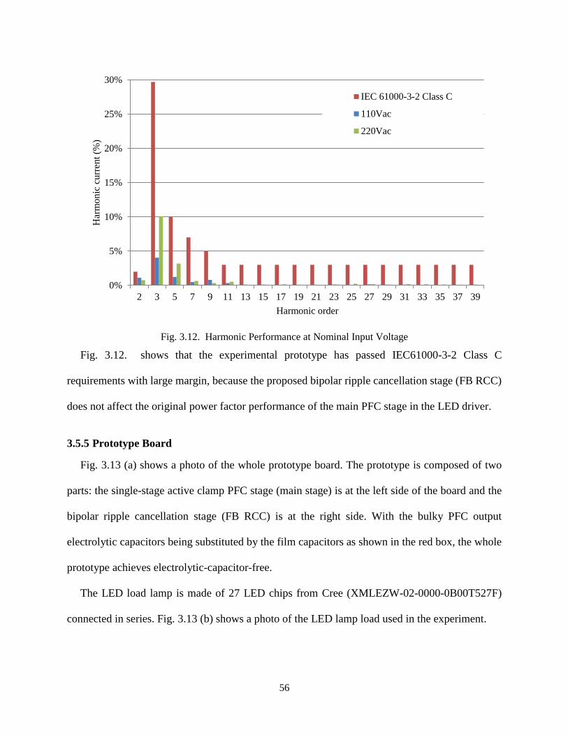
56
Fig. 3.12. Harmonic Performance at Nominal Input Voltage
Fig. 3.12. shows that the experimental prototype has passed IEC61000-3-2 Class C
requirements with large margin, because the proposed bipolar ripple cancellation stage (FB RCC)
does not affect the original power factor performance of the main PFC stage in the LED driver.
3.5.5 Prototype Board
Fig. 3.13 (a) shows a photo of the whole prototype board. The prototype is composed of two
parts: the single-stage active clamp PFC stage (main stage) is at the left side of the board and the
bipolar ripple cancellation stage (FB RCC) is at the right side. With the bulky PFC output
electrolytic capacitors being substituted by the film capacitors as shown in the red box, the whole
prototype achieves electrolytic-capacitor-free.
The LED load lamp is made of 27 LED chips from Cree (XMLEZW-02-0000-0B00T527F)
connected in series. Fig. 3.13 (b) shows a photo of the LED lamp load used in the experiment.
0%
5%
10%
15%
20%
25%
30%
2 3 5 7 9 11 13 15 17 19 21 23 25 27 29 31 33 35 37 39
Har
mo
nic
cu
rren
t (%
)
Harmonic order
IEC 61000-3-2 Class C
110Vac
220Vac

57
Active Clamp Flyback PFC stage
Bipolar Ripple
Cancellation stage
MOSFETs
INPUT CAPs
OUTPUT
CAPs
INDUCTOR
OUTPUT
CAPs of PFC
Stage
(a) Electrolytic-Capacitor-Free LED Driver Photo
(b) LED Lamp Load Photo
Fig. 3.13. Prototype Photos of Bipolar Ripple Cancellation Electrolytic-Capacitor-Free LED Driver.
3.6 Conclusion
This chapter has proposed a new high-power LED driver configuration with a bipolar ripple
cancellation stage (Full-Bridge Ripple cancellation converter). This cancellation circuit neither
impacts the DC output current nor degrades the power factor, cancelling only the AC ripple at the
PFC output.

58
A 100W (150V/0.7A) experimental prototype was built. It has been verified by the
experimental that the proposed technology has significantly reduced the output capacitor by 99%.
At the meantime, the lifespan of the LED driver is extended by 9 times by replacing the electrolytic
capacitor (5,000 hours’ lifespan) on the conventional LED driver with film capacitor (50,000 hours’
lifespan) and making it “electrolytic-capacitor-free”.
For the power efficiency improvement point of view, the proposed configurations can increase
the power conversion efficiency of conventional high power LED driver configuration from 89%
to 92% (verified by the experiment), which might result in a huge energy saving, considering that
the electric lighting consuming 19% of total global electricity production annually [4].

59
Chapter 4
Improved Bipolar Ripple Cancellation Method Using Floating Auxiliary
Capacitor
4.1 Introduction
It has been well documented and verified in Chapter 3 that the basic bipolar ripple cancellation
configuration can significantly reduce the total output capacitance requirement of LED driver
without sacrificing the power factor (PF), thus enabling the use of long-life film capacitors. Most
importantly, bipolar ripple cancellation converter features reduced voltage stresses of the auxiliary
stage components and thus can provide a high efficiency, which is especially desirable for high-
power LED drivers. However, with basic bipolar ripple cancellation technology, the auxiliary stage
requires an auxiliary winding from the main stage. This increases the cost as well as the complexity
of the circuit design. Moreover, with the auxiliary winding, the voltage stresses of the components
in the auxiliary stage is associated with the LED voltage, rather than the low frequency AC voltage
ripple that is necessary to be treated. This results in the overdesign of components voltage stress
under the low LED voltage operation for the LED driver application with variable output voltage
requirements.
In this chapter, an improved bipolar ripple cancellation technology using floating auxiliary
capacitor is proposed. By innovatively controlling the power flow of this auxiliary circuit, the
auxiliary winding can be removed and the auxiliary stage input voltage can be decoupled with the
LED output voltage, thus making the input side of the auxiliary circuit floating and rendering a
more cost effective and more flexible solution for both isolated and non-isolated LED drivers.
With the proposed technology, the input floating auxiliary capacitor voltage is independent of the
LED voltage and is regulated by a control loop. This avoids the overdesign of the voltage stress in
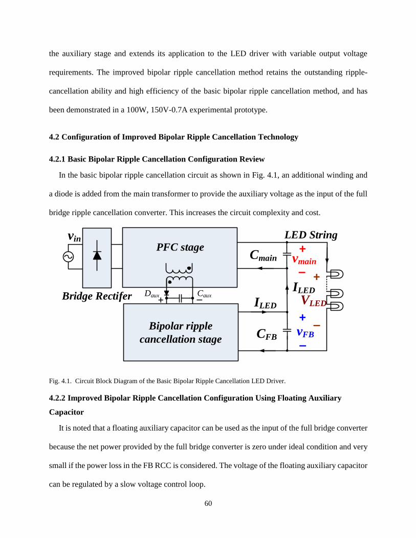
60
the auxiliary stage and extends its application to the LED driver with variable output voltage
requirements. The improved bipolar ripple cancellation method retains the outstanding ripple-
cancellation ability and high efficiency of the basic bipolar ripple cancellation method, and has
been demonstrated in a 100W, 150V-0.7A experimental prototype.
4.2 Configuration of Improved Bipolar Ripple Cancellation Technology
4.2.1 Basic Bipolar Ripple Cancellation Configuration Review
In the basic bipolar ripple cancellation circuit as shown in Fig. 4.1, an additional winding and
a diode is added from the main transformer to provide the auxiliary voltage as the input of the full
bridge ripple cancellation converter. This increases the circuit complexity and cost.
vin
Cmain
CFB
+
_
+
_
+
_
ILED
ILED
vmain
vFB
LED String
Bridge Rectifer VLED+ _CauxDaux
Bipolar ripple
cancellation stage
PFC stage
Fig. 4.1. Circuit Block Diagram of the Basic Bipolar Ripple Cancellation LED Driver.
4.2.2 Improved Bipolar Ripple Cancellation Configuration Using Floating Auxiliary
Capacitor
It is noted that a floating auxiliary capacitor can be used as the input of the full bridge converter
because the net power provided by the full bridge converter is zero under ideal condition and very
small if the power loss in the FB RCC is considered. The voltage of the floating auxiliary capacitor
can be regulated by a slow voltage control loop.

61
Fig. 4.2 shows the block diagram and the key waveform of the proposed LED driver
configuration with floating auxiliary capacitor full bridge ripple cancellation converter. This
improved bipolar ripple cancellation configuration is suitable for both isolated and non-isolated
single-stage PFC topologies.
Since the high-power LED bulbs usually require electrical isolation, the isolated Flyback
topology is still used as the PFC stage to demonstrate the power structure. The architecture of the
LED driver with proposed floating auxiliary capacitor FB RCC is shown in Fig. 4.3.
The FB RCC is still comprised of four switches (Q1~Q4), one inductor (LFB) and two capacitors
(input capacitor Caux and output capacitor CFB). The CFB is of a quite small value (<5µF) to filter
out the high switching frequency noise.
The difference between the LED driver prototype with improved bipolar ripple cancellation
technology and the prototype with the basic one is that there is no second secondary winding. Also,
the rectified diode is removed from the primary side of PFC stage to the bipolar ripple cancellation
converter.

62
Isolated/non-isolated
PFC stage
vin
Cmain
CFB
+
_
+
_
+
_
ILED
Bipolar ripple
cancellation stage
vmain
vFB
LED String
Bridge Rectifer VLED
Caux
(a)
0V
0V
Vripple
vmain
VLED
vFB
0V
Vripple
VDC
(b)
Fig. 4.2. Floating Auxiliary Capacitor Bipolar Ripple Cancellation Principle: (a) Circuit Block Diagram (b) The Key
Waveforms

63
vin
LFB
CFB
Q1 Q2
Q3 Q4
LED
String
Cmain
T
LmCclamp
Qmain
Qaux
+
_
VLED
Clump
Bridge Rectifier Active Clamp Single-Stage Flyback PFC Stage
Floating Capacitor Full-Bridge Ripple Cancellation Converter
D1 D2
D4D3
Lext Llek
Np Ns
Caux
Dmain
Fig. 4.3. Implementation of Floating Auxiliary Capacitor Full-Bridge Bipolar Ripple Cancellation LED
Driver Architecture.
4.3 Control Scheme to Achieve Both Ripple Cancellation and Floating Auxiliary Capacitor
Voltage Regulation
The complete control block diagram of the improved ripple cancellation converter is shown in
Fig. 4.4. The basic AC ripple cancellation control blocks are in Fig. 4.4 in the dotted black boxes.
The basic ripple cancellation control processes have already been elaborated in the previous
chapter 3.2.2, which must feature a bandwidth much higher than 120Hz to provide a quick AC
reference tracking ability.
The significant difference between the control strategies of the two proposed power structures
lies in the method to offset the power loss in the FB RCC. In order to ensure a good ripple
cancellation ability of the proposed floating auxiliary capacitor FB RCC, a power loss offset loop
is added to the basic bipolar ripple cancellation loop, which is highlighted in a red box in Fig. 4.4,
where the FB RCC floating auxiliary capacitor voltage (vCaux) is regulated through a slow PI
control loop. This extra control helps to avoid the under-cancellation phenomenon described as
follows.

64
+_
VCaux_ref
VCaux
Q1
Q2 Q3
Q4
Slow PI
Full Bridge RCC Loss Offset Control Loop
-+
vspwm1
vCaux
_+
vFB
vmain_ripple
Bipolar Ripple Cancellation
vspwm_sum0V
0V
0V
+_
0V
comparator
0V
FB RCC Floating Capacitor Voltage
0V
vspwm2SPWM generator
&
&
Saw-tooth wave
DC Blocking &
180º Phase Shift1/K
1/K
vmain
0V
VDC
vFB
0V
vFB_atten
0V
Fast PI
Fig. 4.4. Combined Control Scheme of Floating Auxiliary Capacitor Bipolar Ripple Cancellation Control Strategy.
4.3.1 Under-Cancellation Phenomenon
When the voltage of the main output is higher than the LED DC output voltage, the FB RCC
will provide a negative voltage to cancel the ripple and the energy will flow into the FB RCC.
When the voltage of the main output is lower than the LED DC output voltage, the FB RCC will
provide a positive voltage to cancel the ripple and the energy will flow out of the FB RCC. If the
FB RCC is lossless, the sum of the input energy and the output energy in a half line cycle will be
equal, and thus the Caux voltage will be self-balancing and vFB presents a symmetrical AC curve,
as shown in Fig. 4.5 (a). In this case, the FB RCC provides a pure AC voltage with zero DC bias,
which is identical with the case when the cancellation loss is offset via the secondary transformer
winding as shown in Fig. 4.1.
However, the FB RCC has power loss in practical implementation. If the Caux voltage is not
regulated or there is no loss offset mechanism, the input energy to the full bridge RCC stage will
be less than the output energy in a half-line cycle, then the Caux will be discharged and the Caux
voltage will drop. When the Caux voltage is sufficiently low, the FB RCC can no longer produce
the peak voltage required to cancel the main stage’s ripple at valley points, and then under-
cancellation may occur. This phenomenon is shown in Fig. 4.5 (b), where periodical bumps occur
on top of DC LED voltage at double line frequency.

65
vmain
vFB
VLED
0V
0V
0V
VDC
VDC
0V
(a) Ideal case
vmain
vFB
VLED
0V
0V
0V
Under cancellation
VDC
VDC
(b) Without loss offset loop
vmain
vFB
VLED
0V
0V
0V
Positive Voltage bias
Negative Voltage bias
VDC
VDC
0V
(c) With Proposed Loss Offset Loop
Fig. 4.5. Under-cancellation Phenomenon Analysis.

66
To solve this problem, the average Caux voltage must be regulated, as shown in the red box in
Fig. 4.4. This loop allows the FB RCC to absorb slightly more input energy than the output energy
in each double line frequency cycle in order to offset the energy loss. As a result, the Caux voltage
can be kept stable and its average value can be regulated at the reference value (VCaux_ref).
According to the electrical features of FB RCC topology, inequality (3-10) must be satisfied to
achieve the fully ripple cancellation.
_
1
2auxC FB pk ripplev V V (4-1)
where vCaux is the Caux voltage which contains a 120Hz voltage ripple component on the top of
its average DC voltage. The VFB_pk is the peak value of the FB RCC output voltage (vFB), which is
decided by the PFC output voltage ripple, Vripple.
4.3.2 Combined Control Scheme
In order to accommodate both two feedback loops in the floating auxiliary capacitor FB RCC
controller to handles the following two tasks, separately: (i) tracking the shape and magnitude of
the periodic AC ripple and (ii) offseting the auxiliary stage loss, a combined bipolar ripple
cancellation control strategy is proposed, which is illustrated in Fig. 4.4.
This control strategy is under the assumption that the FB RCC loss changes quite slow so that
it can be considered as a DC value in one half-line cycle, which is practical for a fixed-load LED
driver.
As shown in Fig. 4.4, the fast PI loop tracks the AC ripple reference (vripple_main) and provides
an ideal SPWM control output (vspwm1) while the slow PI loop regulates the floating auxiliary
capacitor voltage (VCaux) which generates a DC control voltage (vspwm2).These two controlling
outputs are added together as vspwm_sum and then compared to the saw-tooth wave to generate the

67
SPWM driver signals for the four switches in FB RCC. As a result, FB RCC outputs a reversed
AC voltage ripple with a very small negative DC voltage bias, as shown in Fig. 4.5 (c).
It should be noticed that this negative DC voltage bias in the FB RCC output (vFB) will not
affect AC ripple reference (vripple_main) and the normal operation of the fast loop in the basic bipolar
ripple cancellation because this is a DC signal (according to the assumption). All the DC
information existing in the PFC output is blocked by the analog differential circuit before it
becomes the reference for the fast loop. Therefore, the reference signals of these two loops are
decoupled and both loops are able to operate stably and simultaneously.
4.3.3 Full Bridge RCC Floating Auxiliary Capacitor Design
In order to avoid the under-cancellation phenomenon as shown in Fig. 4.5 (b), the Caux value is
critical. Its voltage changes periodically at double line frequency, corresponding to energy
exchanging inside the FB RCC. The design should ensure that the voltage across Caux is always
higher than the auxiliary output voltage, vFB, at any time instant.
The instant Caux input voltage is composed of a DC average voltage and a changing double-
line-frequency voltage ripple resulting from the charging and discharging of the capacitor by the
LED current, ILED.
_ _aux aux avg aux rippleC C Cv V v (4-2)
According to the operation modes of ripple cancellation stage, the input capacitor is charged
when Q2 and Q3 are conducted (Q1 and Q4 are off) and it is discharged when Q1 and Q4 are
conducted (Q2 and Q3 are off). These two intervals are shown in the following equations,
separately.
arg (1 )ch e swT T D (4-3)
argdisch e swT T D (4-4)

68
where Tsw is the switching period of cancellation stage. D is duty cycle of the driving signals
for Q1 and Q4, shown in the following equation.
1 1
( ) sin(2 )2 2
D t M t (4-5)
where ω is angular frequency of line voltage and M is the modulation index of SPWM,
expressed as (4-6).
_
1
2
aux avg
ripple
C
V
MV
(4-6)
Since the average current going through the switches is fixed by the load, the difference between
charging time and discharging time of each switching cycle determines the behavior of input
current, leading to the increase or decrease of the input voltage. The charge for each cycle can be
expressed by the following equation.
arg arg arg( ) ( ( ) ( )) sin(2 )disch e LED disch e ch e LED swQ t I T t T t I T M t (4-7)
The sum of discharge is expressed in the following equation.
arg _ arg
0 1
( ) ( ) sin(2 )swnT n
disch e sum sw disch e LED sw sw
t k
Q nT Q t I T M kT
(4-8)
According to the characteristics of the two-level SPWM modulation strategy, the discharging
period is always longer than the charging time during the first half line cycle before it enters the
other half line cycle. Therefore, the input capacitor keeps discharging over each switching cycle
and its voltage keeps decreasing until it touches the valley at the half cycle point. Then, the biggest
voltage drop can be calculated in the following equation.
_
arg _ ( )4
aux ripple
linedisch e sum
C
aux
TQ
VC
(4-9)
In fact, this is the worst case because the output voltage is on the peak value simultaneously.
Qdischarge_sum(Tline/4) in (4-9) can be simplified into (4-10) after the mathematical deduction.

69
4
arg _
1
4( ) sin( )
24tan( )
line
sw
T
T
line sw LED swdisch e sum LED sw
swk line
line
T T I M TQ I M T k
TT
T
(4-10)
Since Tsw<<Tline (fsw>>fline),
2 2
tan( )sw sw
line line
T T
T T
(4-11)
Then (4-11) can be further simplified, as shown in (4-12).
arg _ ( )4 2
line LEDdisch e sum
line
T I MQ
f
(4-12)
where fline is the AC line frequency.
Therefore, FB RCC is able to work normally for the entire half line cycle as long as the input
valley voltage is set higher than the peak output voltage. The final floating auxiliary capacitor Caux
design rule is shown in the following expression.
_ _ _
arg _
_ min
1( )4
4aux ripple aux avg aux ripple
disch e sum lineLED ripple
aux
C line C C
Q T I VC
V f V V
(4-13)
4.4 Analysis of Proposed Floating Auxiliary Capacitor Bipolar Ripple Cancellation Stage
In Fig. 4.6, two modes of the bipolar ripple cancellation converter using floating auxiliary
capacitor are shown.
Since the RCC's output current is the LED current (a DC current), from a power flow point of
view, the RCC stage is different from the traditional single-phase full bridge inverter in that the
circuit does not transmit DC power to the LED load. The reason is that the load current flowing
direction is always fixed (e.g. from node A to node B in Fig. 4.6 (b)) while the output voltage is
alternating reversing from negative to positive and then back to negative about 120 times a second,
making the energy absorbed during the first half of line cycle go back to the load during the second
half of line cycle. The power loss of the bipolar ripple cancellation stage is offset from the output

70
side of FB RCC using floating auxiliary capacitor by using the combined control scheme, so that
the input voltage of the FB RCC is always higher than its output voltage and the cancellation can
be committed normally.
LFB
CFB
Q1
vFB
Q3 Q4
+_
Q2
0V
ILED
From PFC stage
To PFC stage
Caux
(a)
+
_Vaux
Operating mode 1
Q1
Q3 Q4
Q2 LFB
CFB
+
_Vaux
Operating mode 2
Q1
Q3 Q4
Q2 LFB
CFB
Node B Node A Node B Node A
+_Caux
+_Caux
(b)
Fig. 4.6. Floating Auxiliary Capacitor Bipolar Ripple Cancellation Converter Operation. (a) Stage Prototype. (b)
Operation Modes
The proposed bipolar ripple cancellation methods (with FB RCC) provide the following
advantages, compared to the basic bipolar ripple cancellation method:
4.4.1 Low-Voltage-Stress Power Structure Applicable for both Isolated and Non-Isolated
PFC Topologies
The four MOSFETs Q1~Q4 conduct diagonally to provide paths for the output current ILED as
shown in Fig. 4.6 (b). According to the electrical features of full bridge RCC topology, it sees the
component stress equal to half of the double line frequency ripple, shown in (4-14).
,max
1
2FB rippleV V (4-14)
where VFB, max is the switches’ voltage stress in the FB RCC.
71
Therefore, the proposed bipolar ripple cancellation method presents a double voltage ripple
cancellation ability (given the components voltage stress in the additional stage are the same),
compared to the existing unipolar cancellation method in [44-46], which is more beneficial for
high power high voltage LED driver applications, where low cost of auxiliary circuits are required.
With the help of an extra voltage regulation loop, the cancellation stage loss is offset from the
output side of the FB RCC. Therefore, no auxiliary winding is required for the improved bipolar
RCC with a floating auxiliary capacitor, making it a more cost effective and more flexible solution
applicable for both isolated and non-isolated LED driver applications.
4.4.2 No Overdesigning for Variable-Output-Voltage LED Drivers
In order to adept different LED-load combinations, sometimes, customers require the LED
drivers to handle a wide output voltage range under the rated output current. The ratio of the highest
specification over the lowest one is usually more than 2 times (e.g. VLED=60~150V).
With the basic bipolar cancellation technologies in Chapter 3, given the auxiliary winding turn
ratio is fixed, the component voltage rating has to be overdesigned under the low output voltage
operation (e.g. VLED<150V) to fit the voltage stress at the highest output voltage operation (e.g.
VLED=150V), resulting a non-optimal solution. This is a limitation of this basic bipolar ripple
cancellation configuration proposed in Chapter 3 when it is used in variable output voltage LED
driver.
This is because the input side of bipolar RCC is connected with the auxiliary winding, resulting
the voltage stress of the auxiliary stage associated with the PFC stage output voltage, Vmain, which
is equal to the LED voltage, VLED. For example, if the LED voltage, VLED, is decreased from 150V
to 60V while the ILED = 4A, the minimum input voltage will reduced from 30V to 12V with the

72
same turns ratio design of 1:5 in section 3.3.5. As a result, the RCC will not be able to completely
cancel the 120Hz ripple.
As a trade-off, higher turns ratio must be chosen, which can be calculated by (4-15).
_ min2
1 _ min
auxs
s LED
VN
N V (4-15)
Where VLED_min is the minimum voltage across the LED lamp. For the LED driver with the
specifications of variable output voltage (60V~150V), turns ratio should be Ns2/Ns1 =30/60=0.5,
so that the bipolar RCC can cancellation the 120Hz voltage ripple when VLED=60V.
However, this is an overdesign for the case when VLED=150V, because the minimal input
voltage of bipolar RCC, Vaux_min, will be increase from 35V to 75V when the voltage ripple value
is the same according to (1-2). Therefore, the full bridge MOSFETs with higher voltage stress have
to be used (e.g. 100V), resulting in higher component cost and lower auxiliary stage efficiency.
As to the floating auxiliary capacitor bipolar ripple cancellation method in this chapter, the
minimal Caux voltage of FB RCC, vCaux, should be larger than the peak ripple voltage at the main
output, 0.5Vripple (by around 10%) to ensure the full cancellation of the double line frequency
voltage ripple, according to equation (4-14).
(1-2) shows that the peak to peak value of the double line frequency voltage ripple in PFC
output, Vripple, is only proportional to the LED output current ILED as well as the PFC output
capacitance Cmain, given the line frequency fline is fixed. Therefore, the voltage stress of the floating
auxiliary capacitor (Caux) is designed based on the highest LED current ILED as the worst case (In
this chapter, 0.7A is the rated load current).
Compared to the existing ripple cancellation technologies proposed in [44-46] as well as the
basic bipolar ripple cancellation method in Chapter 3 where the input capacitor voltage is decided

73
by the LED driver DC output voltage (because the input capacitor is connected by an auxiliary
winding from the PFC stage), the proposed floating auxiliary capacitor FB RCC features
significantly reduced component voltage stress and energy loss. As a result, this improved bipolar
ripple cancellation method solves the existing overdesigning problem on the component voltage
rating in FB RCC at low output voltage operation for variable-output-voltage LED drivers and
saves the components’ cost in the auxiliary circuits.
4.4.3 High Efficiency
The bipolar ripple cancellation method also yields a high efficiency, since the FB RCC does
not contribute DC power to the LED load. Without the auxiliary winding, the improved bipolar
ripple cancellation method presents even higher efficiency benefiting from removing the loss in
the auxiliary winding (Ns2) and diode (Daux), shown in Fig. 4.3. This will be demonstrated in the
experimental result.
4.4.4 Portable to Existing LED Driver Products to Achieve Electrolytic-capacitor-free and
Flicker-Free
With the input capacitor being floating, the improved bipolar ripple cancellation converter is
decoupled from both the main PFC stage and the primary side control loop, making it quite easy
to assemble with the existing LED driver products, no matter which prototype or the control
method the product is using.
Only two basic output parameters of the existing LED driver product are used to design the
bipolar ripple cancellation converter: the rated LED current and the output capacitance of the LED
driver that is to be combined with. The rated LED current is normally in LED driver product menu
and the output capacitance can be read from the prototype directly. These two parameters allows
the double line frequency voltage ripple value to be calculated by using (1-2) and then the voltage

74
stress as well as the current stress of the auxiliary converter can be determined. Another feasible
way to obtain the voltage stress of the bipolar ripple cancellation converter is measuring the double
line frequency voltage ripple directly from the driver output. Once the ripple cancellation converter
is built, it can be easily assembled with the existing LED driver product to achieve ripple
cancellation or output capacitance value reduction.
One typical application example is to assemble it with the primary-side regulated LED driver,
as shown in Fig. 4.7. Primary-side sensing does not require opto-coupler and secondary-side
circuitry and is therefore a low component count and compact PCB solution, it is high-attractive
in LED lighting with low power rating. With apply the improved RCC to this application, the
original prototype and the primary side control loop can be kept without any modification since
the bipolar ripple cancellation converter and its control circuit are independent from the PFC
prototype and do not impact the input current waveform. As a result, original advantage of the
single-stage primary side controlled LED driver is kept while the bipolar ripple cancellation
converter is simply connected with the secondary side of the LED driver to eliminate the flicker
and reduce the output capacitance.
D1
Q1
VinNpri Nsec
Primary side
controller
Ipri_pk
Tdis
Naux
CFB
Q1 Q2
Q3 Q4
Caux
LED
String+
_
VLED
Floating Capacitor RCC
LFB
Cmain
Primary-side Regulated LED Driver
Fig. 4.7. Implementation of Improved Bipolar Ripple Cancellation Technology on Primary-side Regulated LED
Driver

75
It should be emphasized that the PFC topology (main stage) and control methods are determined
by the application. For the following application of high power LED driver design specified in
Table 4.1, continuous current mode (CCM) active clamp Flyback prototype is a preferable
selection considering its lower component stress and high efficiency, whose advantages have been
narrated in 2.3.2.
4.5 Experimental Verification
A 100W LED driver prototype was built equipped with the improved bipolar ripple cancellation
converter. The key parameters of the experimental LED driver are given in Table 4.1.
Table 4.1. Floating auxiliary capacitor bipolar ripple cancellation LED driver prototype Parameters
Specifications of LED driver
Line input voltage (vin) 85~265V
LED output voltage (VLED) ≈150V
LED output current (ILED) 0.7A
Out power (PO) 100W
Line frequency (f) 60Hz
Active Clamp Single-stage Flyback PFC Stage
Output Capacitor (Cmain) 56 µF (250V Film Cap)
Switches (Qmain Qaux) SPP11N80C3
Diode (D) C3D16060
Turns Ratio (Np:Ns) 1.2:1
Magnetizing Inductance (Lm) 1300 µH
Internal Leakage Inductor (Llek) 33 µH
External Leakage Inductor (Lext) 15 µH
Active Clamp Capacitor (Cclamp) 68 nF×4 (400V Film Caps)
Single-stage PFC Controller NCP1652A
Floating auxiliary capacitor Bipolar RCC stage
Switching Frequency (fsw) 156 KHz
Input Capacitor (Caux) 10 µF×10
(50V 1206 Ceramic Cap)
Output Inductor (LFB) 50 µH
Output Capacitor (CFB) 4.7 µF
(50V 1206 Ceramic Cap)
MOSFETs (Q1~Q4) TPH11006NLLQCT ×4
(60V, 11mΩ)
LED String Load
LED Chip Part Number XMLEZW-02-0000-0B00T527F×27
Forward Voltage/pcs (Vf) Typ 6 V
Max Current (Imax) 2 A
Luminous Flux/pcs @ 670 mA 270 lm

76
The PFC stage output capacitor (Cmain) is selected as 56 µF, so that peak to peak value of PFC
output voltage ripple (Vripple) is 37V, according to (1-2), which is equal to the peak to peak output
voltage of FB RCC.
In order to satisfy the inequality (4-14), the average value of the input capacitor voltage,
VCaux_avg, is selected as 35V with a maximum 10V peak to peak ripple, VCaux_ripple. So that the
allowed minimum input voltage is 30V which is a reasonable value to ensure the bipolar
cancellation of the FB RCC.
All the parameters for Caux design are listed in Table 4.2.
Table 4.2. Bipolar RCC floating auxiliary capacitor Caux design parameters
Tsw Vripple VCaux_avg VCaux_ripple
1/156kHz 34V 35V 10V
Substituting the values in Table 4.2 into equations (4-13) yields a minimal requirement
(Caux≥91µF) for FB RCC input capacitance (Caux) to avoid under cancellation phenomenon. Caux
is selected as 100µF in the prototype (10µF×10 pieces 50V 1206 Ceramic Caps).
Fig. 4.8 shows that the FB RCC stage input voltage vCaux is regulated at 35±5V by the proposed
loss offset loop. The FB RCC stage exhibits a slight negative DC voltage bias of 1.2V at the FB
RCC stage output voltage. This experimental result validates the previous analysis for Fig. 4.5 (c).

77
Vbais = -1.2V
VCaux_avg=35V
VLED=148.5V
0V
Vcomp_avg
Vmain_avg=149.7V
(CH1:Vmain_dc) VCaux_ripple=10V
CH1: PFC stage output voltage (vmain)CH2: FB RCC output voltage (vcomp)
CH3: LED string voltage (VLED) CH4: FB RCC floating cap voltage (vCaux)
Fig. 4.8. Key Experimental Waveforms of Floating Auxiliary Capacitor Bipolar Ripple Cancellation, When
Vin=110Vac, VLED≈150V, ILED=0.7A, PO=100W
Fig. 4.9 (a) shows that the improved bipolar ripple cancellation method produces a smaller LED
driving current ripple @120Hz (7.8mA RMS) with only 56µF output capacitance(Cmain), compared
to a higher 8.2mA RMS current ripple in the conventional single-stage LED driver, where 4700µF
output capacitance is required, shown in Fig. 4.9 (b). Therefore, the total required output
capacitance of conventional signal-stage solution is reduced by 99%!
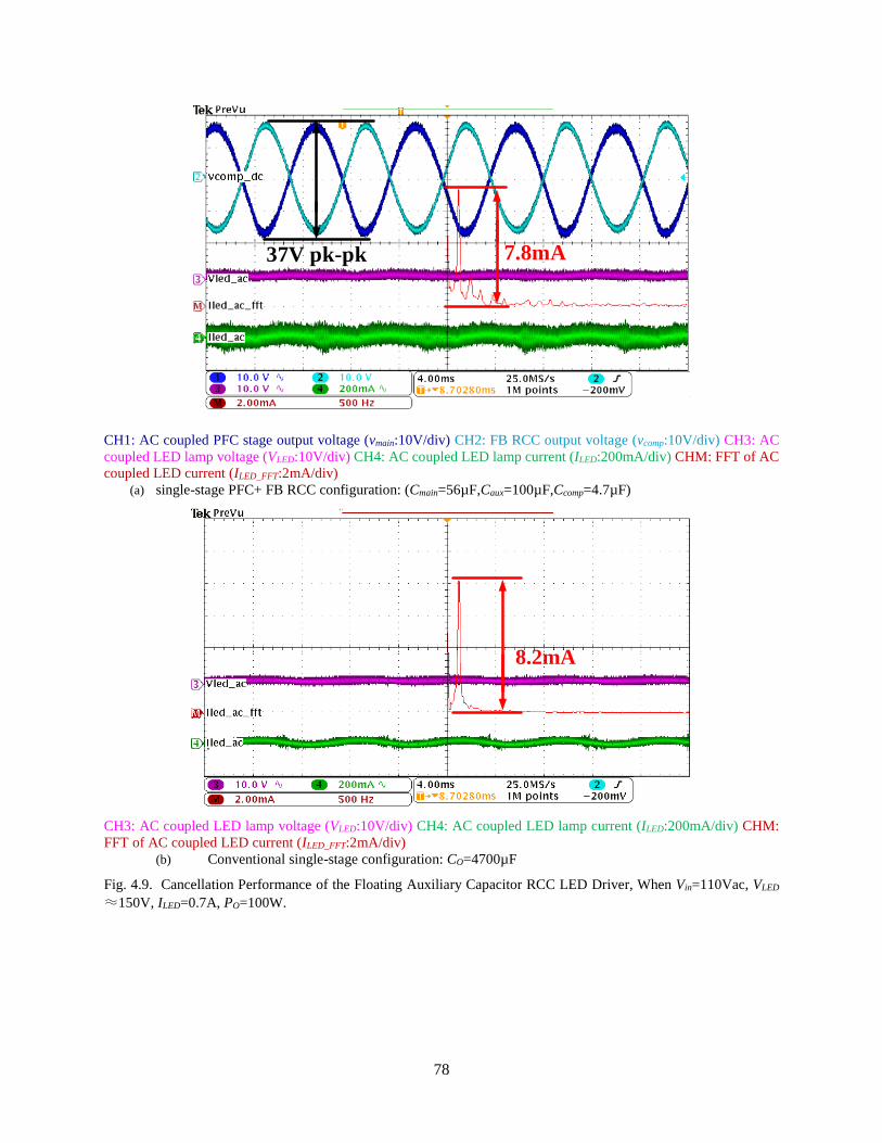
78
7.8mA37V pk-pk
CH1: AC coupled PFC stage output voltage (vmain:10V/div) CH2: FB RCC output voltage (vcomp:10V/div) CH3: AC
coupled LED lamp voltage (VLED:10V/div) CH4: AC coupled LED lamp current (ILED:200mA/div) CHM: FFT of AC
coupled LED current (ILED_FFT:2mA/div)
(a) single-stage PFC+ FB RCC configuration: (Cmain=56µF,Caux=100µF,Ccomp=4.7µF)
8.2mA
CH3: AC coupled LED lamp voltage (VLED:10V/div) CH4: AC coupled LED lamp current (ILED:200mA/div) CHM:
FFT of AC coupled LED current (ILED_FFT:2mA/div)
(b) Conventional single-stage configuration: CO=4700µF
Fig. 4.9. Cancellation Performance of the Floating Auxiliary Capacitor RCC LED Driver, When Vin=110Vac, VLED
≈150V, ILED=0.7A, PO=100W.

79
Fig. 4.10 shows the input voltage and input current waveform of floating auxiliary capacitor
bipolar cancellation method (vin=110Vac), which has achieved a high PF of 0.994. Both of the
improved bipolar ripple cancellation technology and the basic bipolar ripple cancellation
technology are implemented and verified on the same Flyback PFC prototype, therefore the LED
driver with floating auxiliary capacitor RCC presents the similar power factor and harmonic
performance (as shown in Fig. 4.11 and Fig. 4.12), which has also passed IEC61000-3-2 Class C
requirements with large margin.
PF=0.994
iin
vin=110Vac
VLED
CH1: AC input voltage (vin) CH2: AC input current (iin) CH3: LED string voltage (VLED)
Fig. 4.10. Input Current and Output Voltage of the Floating Auxiliary Capacitor Bipolar RCC LED driver, when
Vin=110Vac, VLED≈150V, ILED=0.7A, PO=100W

80
Fig. 4.11. Power Factor Comparison of The LED Driver With Floating auxiliary capacitor RCC and Winding-
connected RCC and At Full Load, When Cmain=56 µf, VLED≈150V, ILED=0.7A, Po=100W.
Fig. 4.12. Harmonic Performance of Floating Auxiliary Capacitor RCC LED Driver at Nominal Input Voltage
0.900
0.910
0.920
0.930
0.940
0.950
0.960
0.970
0.980
0.990
1.000
80 110 140 170 200 230 260
Pow
er F
acto
r
Input voltage (V)
with auxiliary winding
with floating cap
0%
5%
10%
15%
20%
25%
30%
2 3 5 7 9 11 13 15 17 19 21 23 25 27 29 31 33 35 37 39
Harm
on
ic c
urr
ent
(%)
Harmonic order
IEC 61000-3-2 Class C
110Vac
220Vac

81
Meanwhile, the experimental prototype of improved ripple cancellation technology with
floating auxiliary capacitor yields higher system efficiency, compared to the basic one. The
experimental results under the universal AC input are shown in Fig. 4.13, where a peak system
efficiency of 92.4% has been achieved. The power loss with only conventional single-stage PFC
stage and the power loss of the PFC stage plus cancellation stage are measured separately, the
difference between these two is the loss of the cancellation stage. The FB RCC stage loss is
generally less than 1% under different input voltage, as shown in Fig. 4.14.
The peak efficiency of the system is 92% for the winding-connect bipolar ripple cancellation
and 92.4% for the improved bipolar ripple cancellation with floating auxiliary capacitor. In general,
the floating auxiliary capacitor bipolar ripple cancellation method presents a slightly higher
efficiency than the one with auxiliary winding by 0.4%. This slight improvement is introduced by
the loss in extra winding (Ns2) and the diode (Daux) from the main PFC stage.
(a) System efficiency.
Fig. 4.13. Power Conversion Efficiency Comparison of LED Driver With Floating Auxiliary Capacitor RCC and
Winding-connected RCC and At Full Load, When Cmain=56 µf, VLED≈150V, ILED=0.7A, Po=100W.
89.09
89.98
90.98
91.94 91.92 91.96 91.8391.55
91.2390.8289.72
90.61
91.39
92.3 92.37 92.3992.07 91.85
91.5491.14
85
86
87
88
89
90
91
92
93
94
80 110 140 170 200 230 260
Eff
icie
ncy
(%)
Input voltage (V)
with auxiliary winding
with floating cap

82
Fig. 4.14. Floating auxiliary capacitor RCC stage loss in LED driver when VLED≈150V, ILED=0.7A, Po=100W.
Dimming performance of the proposed LED driver is also measured down to 50% load (This
is normally the lowest output power working conditions with PF requirement for LED light) and
the results are shown in Fig. 4.15. According to the experimental results, the half-load (PO=50W,
VLED≈150V) system efficiency are generally higher than 88.5% and the PF are over 0.9 under both
the nominal input voltages (110Vac and 220Vac).
0.54W
0.92W
0.65W 0.69W 0.71W0.81W 0.85W
0.94W
1.14W
0
0.5
1
1.5
2
100 120 140 160 180 200 220 240 260
Loss
(W
)
input voltage (Vac)
FB RCC loss @ different input voltage
FB RCC loss @ different input voltage

83
(a) System efficiency.
(b) Power factor.
Fig. 4.15. Dimming Performance of the LED Driver With Floating Capcitor RCC, When Cmain=56µf, VLED≈150V.
88.6589.45
90.1390.48
90.8189.20
90.1290.88
91.5291.86
82.00
84.00
86.00
88.00
90.00
92.00
50 60 70 80 90 100
Eff
icie
ncy
(%
)
Output power(%)
Efficiency performance under dimming
Eff @110V
Eff @ 220V
0.9710.976
0.9860.99 0.991
0.9
0.925
0.95
0.9630.968
0.86
0.88
0.9
0.92
0.94
0.96
0.98
1
50 60 70 80 90 100
PF
Output power(%)
PF performance under dimming
PF @ 110V PF @ 220V
84
4.6 Conclusion
This chapter proposes a novel electrolytic-capacitor-free solution for single-stage high-power
LED driver with bipolar ripple cancellation converter (FB RCC) using a floating auxiliary input
capacitor. It features very low voltage stress, very small output capacitance, and very low LED
driving current ripple. It is applicable to both isolated and non-isolated single-stage LED drivers.
The required total output capacitance is only 1.2% of conventional methods, and thus electrolytic
capacitors can be removed.
By innovatively controlling the power flow of the FB RCC, the auxiliary winding can be
removed from the basic bipolar ripple cancellation method proposed in Chapter 3, rendering a
more cost effective and more flexible solution for both isolated and non-isolated LED driver
applications which provides the attractive characteristic that the FB RCC input voltage can be
regulated separately from the main PFC stage output voltage, avoiding the overdesigning of the
component voltage rating in the cancellation stage at low output voltage operation for the variable-
output-voltage LED drivers.
A 100W (150V/0.7A) experimental prototype was built. The experimental results demonstrate
that, using a 56µF output capacitor, the double line frequency LED ripple current can be as low as
7.8mA RMS in the proposed configuration, which would otherwise require over 4700µF output
capacitance using conventional single-stage LED drivers.

85
Chapter 5
Current Sensing Control Method for Bipolar Ripple Cancellation Technology
5.1 Introduction
The basic bipolar ripple cancellation technology is proposed for single-stage offline high power
LED driver in Chapter 3 to reduce the output capacitance requirement, enabling the use of long
life film capacitor instead of the short life electrolytic capacitor. In Chapter 4, an improved bipolar
ripple cancellation configuration is proposed to extend its application to the LED driver with
variable output voltage, avoiding the overdesign of the voltage stress of components in the
auxiliary power structure.
In this chapter, a new current-sensing-based control strategy for the bipolar ripple cancellation
converter will be proposed, which eliminates LED light flicker caused by Power Factor Correction
(PFC) stage and significantly reduces its output capacitance requirement. Instead of sensing two
differential output voltage signals as in existing voltage-ripple-based control strategy, the proposed
current-sensing-based control strategy achieves ripple cancellation only by sensing the LED
current information, which significantly simplifies the control circuitry. In addition, the proposed
control strategy allows input voltage of the bipolar ripple cancellation converter (RCC) to tightly
track its output voltage peak value with no extra control circuit, thus minimizing the RCC
component voltage stress as well as the RCC loss. A 100W, 150V-0.7A experimental prototype
has been built to demonstrate the advantages of the proposed control method.
5.1.1 Background
It has been pointed out that the low-frequency current ripple in the LED output current will
cause LED flicker problem that is harmful to human visual system [26, 28, 63].

86
The principle of bipolar ripple cancellation technology is to cancel the double line frequency
ripple voltage from the single-stage LED driver using an additional small power converter (bipolar
ripple cancellation converter) that is connected in series with the PFC output. As a result, a pure
DC voltage is obtained and is applied to the LED string to produce DC LED current [44, 64-66].
It has been reported in [44, 64, 65] that the existing RCC can significantly reduce the total output
capacitance of LED driver without sacrificing the Power Factor (PF), thus enabling the use of long-
life film capacitors. Also, RCC features the reduced voltage stresses of the auxiliary stage
components and thus can provide a higher efficiency.
The existing RCC solutions include two categories: (a) winding-connected RCC in Chapter 3
[44, 64, 66] (basic ripple cancellation) and (b) floating auxiliary capacitor RCC [66, 67] (improved
ripple cancellation)in Chapter 4. The winding-connected ripple cancellation method uses an
additional winding from the main transformer to provide the auxiliary voltage as the input of the
ripple cancellation converter (RCC). In Chapter 4, a floating auxiliary capacitor full-bridge-type
ripple cancellation converter is proposed to remove the auxiliary winding and diode from the main
PFC stage by controlling the power flow of this auxiliary circuit with an additional loss offset
control loop, making the input side capacitor of the auxiliary circuit floating and rendering a more
flexible solution for both isolated and non-isolated LED driver applications, as shown in Fig. 5.1.

87
Isolated/non-isolated
PFC stage
vin
CFB
ILED
ILED
Imain
Bridge Rectifer
Caux
Full-Bridge Bipolar Ripple
Cancellation Converter
(FB RCC)
Cmain vmain
vFB
++
Floating
Fig. 5.1. The Floating Auxiliary Capacitor Bipolar Ripple Cancellation LED Driver Method
However, all of the above mentioned ripple cancellation converters proposed in Chapter 3 and
Chapter 4 employ the voltage-ripple-based feedback control strategy and therefore suffer from the
relative complex and uneconomic signal-sensing circuits. The typical block diagram of the existing
voltage-based feedback control strategy is shown in Fig. 5.2 (a), where the two series-connected
output voltages (the main PFC stage output voltage, vmain, and the cancellation stage output voltage,
vFB) are sensed simultaneously to achieve the ripple cancellation. The key block diagrams in the
ripple cancellation loop are highlighted in Fig. 5.2 (a). The corresponding sensing circuit for the
RCC is given in Fig. 5.2 (b) where two differentials to single-end voltage conversion circuits are
required.

88
Cmain
+-
Iref
CFB
Ierr
PFC
controller
LED
Lamp
Full-Bridge RCC+-
vin_sense
vin
Single-stage Flyback
PFC stage
Opto-couplervcomp_p
GC1vcomp_s
Voltage
sensor
AC Voltage
Ripple Sensor
+-GC2
iLED(t)
vrip(t)
vrip_err
vpfc_ctrl vcomp_ctrl
+- +-
vFB(t) vmain(t
)
Primary Side Secondary Side
vmain
vFB
(a) Block Diagram
Vaux
+
-
LFB
CFB
Q1 Q2
Q3 Q4
Caux
SPWM
Generator
vmain(t)
vmain_rip(t)
+-Gc
DBU
vFB(t)
vFB
+
-
PFC output voltage
A2
Differential to single
end conversion
+
-
A1vmain
+
-
Differential to single
end conversion
+
(b) Implementation circuit of RCC part
Fig. 5.2. The Voltage-Ripple-Sensing-Based Control Strategy for Bipolar Ripple Cancellation.

89
A current-sensing-based feedback strategy is introduced to achieve the ripple cancellation based
on sensing LED current only. As the LED current is also a basic controlled item for the main stage
PFC controller, the sensing circuit to achieve Power Factor Correction (PFC) in the main stage can
be also used to achieve ripple cancellation, which significantly simplifies the control circuit.
5.2 Current-sensing-based Feedback Control Strategy
5.2.1 System Block Diagrams
The proposed control strategy is current-sensing-based and consists of two current control loops:
(i) the main PFC stage control loop regulating the average LED current and (ii) the current-sensing-
based control loop suppressing the double-line-frequency LED current ripple. The input side and
output side of PFC stage is isolated (as shown by a double dotted line in the center of the figure).
The complete control diagram is given in Fig. 5.3, where the proposed current-sensing-based
control loop is highlighted in red.
Cmain
+-
Iref
CFB
Ierr
PFC
controller
LED
Lamp
Full-Bridge Bipolar
Ripple Cancellation
Converter
+-
vin_sense
vin
Single-stage Flyback
PFC stage
Opto-couplervcomp_p
GC1vcomp_s
Voltage
sensor
AC Current
Ripple Sensor+-GC2
iLED(t)
Irip_ref=0
irip(t)irip_err
vpfc_ctrl vspwm_ctrl
Primary Side Secondary Side
Bridge Rectifer
Fig. 5.3. Current-sensing-based Control Strategy for Bipolar Ripple Cancellation

90
This highlighted loop includes one AC current ripple sensing block and one compensation
network (GC2). The ripple cancellation rule is straightforward: the double-line-frequency current
ripple (irip) is sensed by blocking the DC component of the LED current (iLED) and then it is
controlled to approach a non-ripple reference (Irip_ref=0), generating the error signal (irip_err). Based
on this error signal, the compensation network regulates the SPWM control signal (vspwm_ctrl) to
force the full-bridge RCC to generate an out of phase double-line-frequency voltage ripple and the
resulting LED current, iLED(t) to be non-ripple (irip=0). In this way, the double-line-frequency
component in the LED current is significantly suppressed. It is noticed from Fig. 5.3 that both the
PFC controller output (vpfc_ctrl) and the proposed current ripple suppression controller output
(vspwm_ctrl) are based on the LED current (iLED), rather than the output voltage signals. Therefore,
the PFC controller and the current ripple cancellation controller share the same LED current
sensing circuit in the proposed control strategy. In practical implementation, to avoid the negative
part of the sensed AC current ripple signal, a level shifter is applied to both the sensed current
ripple (irip) and its reference (Irip_ref=Vbias) in the experiment.
5.2.2 Power Structure and Control Circuit
The power circuit of the flicker-free LED driver with an isolated single-stage Flyback PFC
stage is shown in Fig. 5.4, where a floating auxiliary capacitor full-bridge inverter is used as the
RCC (highlighted in the blue box).

91
vin
LFB
CFB
Q1 Q2
Q3 Q4
LED
String
Cmain
T
LmCclamp
Qmain
QauxClump
Bridge Rectifier Active Clamp Single-Stage Flyback PFC Stage
Floating Capacitor Full-Bridge RCC
D1 D2
D4D3
Np Ns
Caux
Dmain
iLED(t)
Rsense
Lext Llek
Fig. 5.4. The Flicker-Free LED Driver With Full-Bridge Bipolar RCC[67].
The proposed current-sensing-based control strategy simplifies the original controlling circuit
in Chapter 3 and Chapter 4 by removing two differential sensing to single-end voltage conversion
circuits. The detailed control circuit for the FB RCC (the highlighted blue part in Fig. 5.4) is
illustrated in Fig. 5.5.
Vaux
+
-
LFB
CFB
Q1 Q2
Q3 Q4
Caux
SPWM
Generator +-Gc2
irip(t)
AC Current Ripple Sensing
& Level Shift Circuit
Rsense
iLED(t)
To PFC Stage From LED String
+
-
A1
DC Blocking Circuit
+-
Vbias
Vbias
Irip_ref=Vbias +
-Vbias
irip_err
Floating Catacitor Full-Bridge RCC
Compensation Network
SPWM Generator
vspwm(t)
Fig. 5.5. Implementation of Current-sensing-based Control Method.
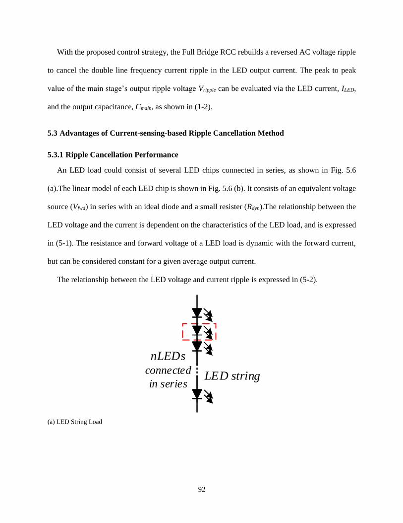
92
With the proposed control strategy, the Full Bridge RCC rebuilds a reversed AC voltage ripple
to cancel the double line frequency current ripple in the LED output current. The peak to peak
value of the main stage’s output ripple voltage Vripple can be evaluated via the LED current, ILED,
and the output capacitance, Cmain, as shown in (1-2).
5.3 Advantages of Current-sensing-based Ripple Cancellation Method
5.3.1 Ripple Cancellation Performance
An LED load could consist of several LED chips connected in series, as shown in Fig. 5.6
(a).The linear model of each LED chip is shown in Fig. 5.6 (b). It consists of an equivalent voltage
source (Vfwd) in series with an ideal diode and a small resister (Rdyn).The relationship between the
LED voltage and the current is dependent on the characteristics of the LED load, and is expressed
in (5-1). The resistance and forward voltage of a LED load is dynamic with the forward current,
but can be considered constant for a given average output current.
The relationship between the LED voltage and current ripple is expressed in (5-2).
LED string
nLEDs connected
in series
(a) LED String Load

93
Single LED
model
Vfwd
Rdyn
Ideal Diode
(b) Equivalent Circuit Model of A Single LED
Fig. 5.6. Equivalent Circuit Model of LED String Load
_LED string fwd
LED
dyn
V nVI
nR
(5-1)
_LED string
LED
dyn
VI
nR
(5-2)
Given the low equivalent resister characteristic as well as the nonlinearity of the LED load,
even a small LED voltage ripple (△VLED_string) may result in a large LED current ripple (△ILED).
This assigns a tough task for the existing strategy proposed in Chapter 3 and Chapter 4 intending
to cancel the current ripple by limiting the voltage ripple when the voltage ripple is too small to be
detected.
In addition, compared to the voltage-ripple-based cancellation method requiring two
differentially sensed voltage signals, the proposed current-sensing-based method only senses the
current ripple and compares it to a zero reference (a DC voltage), potentially avoids the error due
to the mismatch between the two sensing circuits, and thus leading to a more effective solution to
cancel the current ripple.

94
5.3.2 RCC Input Voltage Auto-Tracking to Minimize the RCC Loss at Different Loads
The proposed current-sensing-based method can achieve optimization of the ripple cancellation
with the minimum floating auxiliary capacitor voltage regardless the LED output voltage (VLED)
and loads (ILED) by nature. The mechanism is as follow: As shown in Fig. 5.4, the FB RCC input
voltage Vaux is initially charged to exceed the peak value of Vripple by ILED due to its unidirectional
flowing characteristic and then the voltage start decreasing due to the loss in the FB RCC. This
results Vaux to be less than Vripple where the sinusoidal peaks are lost. The resulting LED current
presents small drop (less than its nominal value) at each valley of vFB. The small distortion makes
the RCC consumes less energy during each positive half cycle than that it receives during each
negative cycle, offsetting the RCC loss. The current bumps are fixed when the energy saved by
the distortion equals to total RCC loss in each 120Hz cycle. As a result, the RCC input voltage is
auto-tuned and kept very close to but a bit less than the peak value of output voltage without extra
input voltage regulation loop. Since the FB RCC loss is in proportional to its input voltage (given
the fixed output AC voltage), with the proposed current-sensing-based method, the FB RCC
component voltage stress and the loss are minimized. It should be noticed that the voltage-ripple-
based control strategy can also achieve auto-tracking but is not sensitive enough for the low-
equivalent-resister LED loads, therefore an additional loss offset loop is added Chapter 4 to
enhance the ripple cancellation performance.
5.4 Experimental Verification
The parameters of a 100W proposed LED driver are shown in Table 5.1.

95
Table 5.1. Current sensing bipolar ripple cancellation LED driver prototype parameters
Specifications of LED driver
Line input voltage (vin) 110V
LED output voltage (VLED) 90~150V
Rated LED output current (ILED) 0.7A
Rated power (PO) 100W
Line frequency (f) 60Hz
Active Clamp Single-stage Flyback PFC Stage
Output Capacitor (Cmain) 56 µF (250V Film Cap)
Switches (Qmain Qaux) SPP11N80C3
Diode (D) C3D16060
Turns Ratio (Np:Ns) 1.2:1
Magnetizing Inductance (Lm) 1300 µH
Internal Leakage Inductor (Llek) 33 µH
External Leakage Inductor (Lext) 15 µH
Active Clamp Capacitor (Cclamp) 470 nF (400V Film Cap)
Single-stage PFC Controller NCP1652A
FB RCC Stage
Switching Frequency (fsw) 156 KHz
Input Floating auxiliary capacitor (Caux) 10 µF×12
(50V 1206 Ceramic Cap)
Output Inductor (LFB) 22 µH
Output Capacitor (CFB) 4.7 µF×1
(50V 1206 Ceramic Cap)
Full-bridge Switches (Q1~Q4) TPH11006NLLQCT ×4
(60V, 11mΩ)
LED String Load
LED Chip Part Number XMLEZW-02-0000-0B00T527F (15~27pcs for
different load combination)
Forward Voltage/pcs (Vf) Typ 6 V
Max Current (Imax) 2 A
Luminous Flux/pcs @ 670 mA 270 lm
5.4.1 Ripple Cancellation Performance
Fig. 5.7 (a) and Fig. 5.7 (b) show that the proposed method produces a very small LED driving
voltage ripple @120Hz (0.23V RMS when VLED=150V; 0.12V RMS when VLED=90V) with only
56µF total output capacitance (Cmain). The AC voltage generated by the FB RCC (CH2, AC
coupled) mitigates the 120Hz PFC ripple (CH1, AC coupled), resulting in a total flat voltage (CH3,
AC coupled) and flat LED current (CH4, AC coupled), the current ripple value @ 120Hz is shown
in FFT channel (CHM). The 120Hz PFC voltage ripple is 37V pk-pk before cancellation. The LED
output current ripple @ 120Hz is 18mA in Fig. 5.7 (a) and 13mA Fig. 5.7 (b) after cancellation.

96
Vripple = 37V
VLED@120Hz=0.23V
(0.62% of Vripple)ILED@120Hz=18mA
CH1: AC coupled PFC stage output voltage (vmain_ac) CH2: DC coupled FB RCC output voltage (vFB)
CH3: AC coupled LED string voltage (VLED_ac) CH4: AC coupled LED string current (ILED_ac)
CHM: FFT of AC coupled LED string current (ILED_ac_FFT) (a)VLED=150V ILED=0.7A (Po=100W, 27 LED chips)
Vripple = 37V
VLED@120Hz=0.12V
0.32% of VrippleILED@120Hz=13mA
CH1: AC coupled PFC stage output voltage (vmain_ac) CH2: DC coupled FB RCC output voltage (vFB)
CH3: AC coupled LED string voltage (VLED_ac) CH4: AC coupled LED string current (ILED_ac)
CHM: FFT of AC coupled LED string current (ILED_ac_FFT) (b) VLED=90V ILED=0.7A (Po=63W, 15 LED chips)
Fig. 5.7. Key Waveforms of the Proposed Current-sensing-based Ripple Cancellation Method, When Vin=110Vac,
ILED=0.7A
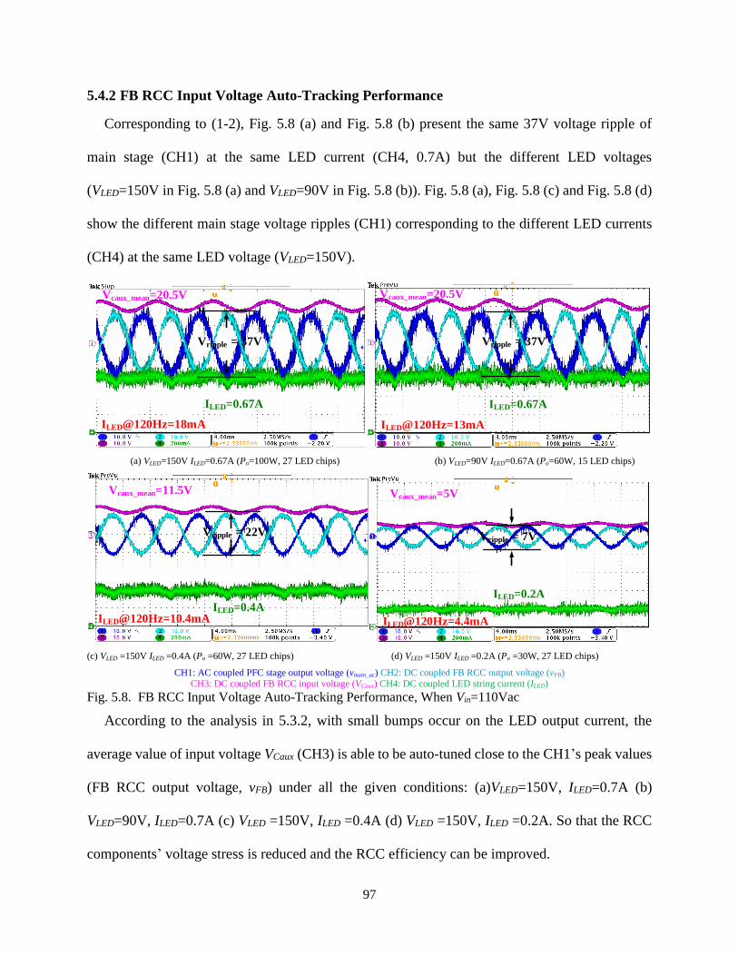
97
5.4.2 FB RCC Input Voltage Auto-Tracking Performance
Corresponding to (1-2), Fig. 5.8 (a) and Fig. 5.8 (b) present the same 37V voltage ripple of
main stage (CH1) at the same LED current (CH4, 0.7A) but the different LED voltages
(VLED=150V in Fig. 5.8 (a) and VLED=90V in Fig. 5.8 (b)). Fig. 5.8 (a), Fig. 5.8 (c) and Fig. 5.8 (d)
show the different main stage voltage ripples (CH1) corresponding to the different LED currents
(CH4) at the same LED voltage (VLED=150V).
Vripple = 37V
ILED=0.67A
Vcaux_mean=20.5V
ILED@120Hz=18mA
Vripple = 37V
ILED=0.67A
Vcaux_mean=20.5V
ILED@120Hz=13mA
(a) VLED=150V ILED=0.67A (Po=100W, 27 LED chips) (b) VLED=90V ILED=0.67A (Po=60W, 15 LED chips)
Vripple = 22V
ILED=0.4A
Vcaux_mean=11.5V
ILED@120Hz=10.4mA
Vripple = 7V
ILED=0.2A
Vcaux_mean=5V
ILED@120Hz=4.4mA
(c) VLED =150V ILED =0.4A (Po =60W, 27 LED chips) (d) VLED =150V ILED =0.2A (Po =30W, 27 LED chips)
CH1: AC coupled PFC stage output voltage (vmain_ac) CH2: DC coupled FB RCC output voltage (vFB) CH3: DC coupled FB RCC input voltage (VCaux) CH4: DC coupled LED string current (ILED)
Fig. 5.8. FB RCC Input Voltage Auto-Tracking Performance, When Vin=110Vac
According to the analysis in 5.3.2, with small bumps occur on the LED output current, the
average value of input voltage VCaux (CH3) is able to be auto-tuned close to the CH1’s peak values
(FB RCC output voltage, vFB) under all the given conditions: (a)VLED=150V, ILED=0.7A (b)
VLED=90V, ILED=0.7A (c) VLED =150V, ILED =0.4A (d) VLED =150V, ILED =0.2A. So that the RCC
components’ voltage stress is reduced and the RCC efficiency can be improved.

98
5.4.3 System Efficiency and Power Factor Correction Performance
With the help of RCC input voltage auto-tracking mechanism, the experimental prototype
shows a system efficiency of 91% and 92% (given vin=110Vac and 220V). Fig. 5.9 shows the
corresponding input voltage and input current waveforms of proposed method, which has achieved
the PFs of 0.990 and 0.953. More experimental results under the universal AC input are shown in
Fig. 5.10, where a peak system efficiency of 92.4% has been achieved. The FB RCC stage loss is
generally less than 1% under different input voltage, as shown in Fig. 5.11.
Vin = 110V
Iin
VLEDPF@110V=0.990
(a) Vin=110V
Vin = 220V
Iin
VLED
PF@220V=0.953
(b) Vin=220V
CH1: AC input voltage (vin) CH2: AC input current (iin) CH3: AC coupled LED lamp voltage (VLED)
Fig. 5.9. Input Current and Output Voltage of the Proposed LED Driver, When Vin=110Vac and 220Vac,
VLED≈150V, ILED=0.7A

99
(a) System Efficiency
(b) Power Factor
Fig. 5.10. Performance of the Floating Auxiliary Capacitor Bipolar RCC LED Driver with Current-sensing-based
Control Method At Full Load, When Cmain=56 µf, VLED≈150V, ILED=0.7A.
89.84
90.89
92.05 92.34 92.43 92.23 91.98 91.791.32
91.01
80
82
84
86
88
90
92
80 100 120 140 160 180 200 220 240 260
Eff
icie
ncy
(%)
Input voltage (V)
0.995
0.9930.99
0.985
0.9780.975
0.9710.966
0.96
0.951
0.9
0.91
0.92
0.93
0.94
0.95
0.96
0.97
0.98
0.99
1
80 100 120 140 160 180 200 220 240 260
Pow
er F
acto
r
Input voltage (V)

100
Fig. 5.11. Full Bridge Converter Loss in Floating auxiliary capacitor Bipolar RCC LED Driver, When VLED≈150V,
ILED=0.7A, Po=100W.
5.4.4 Dimming Performance
Dimming performance of the proposed LED driver is also given in Fig. 5.12. Under both the
nominal input voltages (110Vac and 220Vac), the half-load (PO=50W, VLED≈150V) system
efficiency are generally higher than 88% and the PF are over 0.9.
(a). System Efficiency
0.59W
0.88W
0.6W 0.65W 0.71W0.85W 0.8W
0.94W1.1W
0.59%0.88%
0.60% 0.65% 0.71% 0.85% 0.80% 0.94% 1.10%
0%
1%
2%
3%
4%
5%
0
0.5
1
1.5
100 120 140 160 180 200 220 240 260 Loss
/Ou
tpu
t P
ow
er (
%)
Loss
(W
)
Input voltage (Vac)FB RCC loss @ different input voltage
88.0
89.290.1 90.5 90.8
89.290.0
91.091.5 91.9
80.0
82.0
84.0
86.0
88.0
90.0
92.0
94.0
50 60 70 80 90 100
Eff
Output power(%)
Eff performance under dimming
Eff @110V
Eff @ 220V

101
(b). Power Factor.
Fig. 5.12. Dimming Performance of the LED Driver Under Current-sensing-based Ripple Cancellation Method, When
Cmain=56µf, VLED≈150V.
5.5 Conclusion
This chapter proposes a current-sensing-based control strategy to improve performance and
simplify the control circuitry of the ripple cancellation converter. The proposed scheme is applied
to the previous proposed floating auxiliary capacitor bipolar ripple cancellation converter to
eliminate LED flickering and reduce the required output capacitance, enabling the use of film
capacitor. Also, the proposed method has a unique tracking and efficiency improvement
mechanism under different loads and different output voltage, which has been verified through the
experiment. Extensive experimental results are provided to demonstrate the performance.
0.971
0.976
0.9860.990 0.991
0.90
0.93
0.95
0.960.97
0.860
0.880
0.900
0.920
0.940
0.960
0.980
1.000
50 60 70 80 90 100
PF
Output power(%)
PF performance under dimming
PF @ 110V PF @ 220V

102
Chapter 6
Single-stage LED Driver Using LLC Resonant Converter in PFC Mode
6.1 Introduction
When high power factor is achieved with a single-stage offline LED driver, an energy
imbalance presents between the input side and the output side, regardless of which topologies or
controlling methods are used. The energy imbalance creates a significant double line frequency
voltage ripple across LED, which causes an even larger double line frequency ripple current
through LED. The double line frequency ripple LED current is manifested as the lighting flicker
through LEDs, which is harmful to human’s eyes. In Chapter 3 to Chapter 5, the bipolar ripple
cancellation technologies for single-stage offline LED drivers with different auxiliary power
structures and control methods have been involved: The basic bipolar ripple cancellation
technology was first introduced in Chapter 3 to solve the light flicker issue and remove the fragile
electrolytic capacitor from the offline high power LED driver prototypes without sacrificing the
high power factor. Then the improved bipolar ripple cancellation technology with floating
auxiliary capacitor and the current sensing control method for ripple cancellation power structure
have been proposed and introduced in Chapter 4 and Chapter 5, respectively, to allow the low
voltage rating components be used in the auxiliary bipolar ripple cancellation stage for variable
output voltage LED driver applications and to simplify the control circuits.
Since the auxiliary bipolar ripple cancellation stage only handles the AC voltage (using voltage
ripple sensing control method in Chapter 3 and Chapter 4) or AC current ripple (using current
ripple sensing control method in Chapter 5), the power processed by the auxiliary stage is quite
small (<10% of the total output power), resulting in very small loss. The total LED driver
efficiency depends on the main PFC stage (conventional single stage LED topology), therefore it

103
is essential to improve the main PFC stage power efficiency to further improve the LED driver
with bipolar ripple cancellation.
In this chapter, a high power, high efficiency, single-stage offline LED driver topology is
introduced, where LLC resonant converter is innovatively used as a power factor correction stage
in the LED driver. With the natural soft switching behavior on primary side switches and the
secondary side rectifier diodes, the LLC resonant converter LED driver presents a high efficiency.
The design rule for LLC PFC converter is derived at first. A 240 Watts LED driver prototype is
built to verify the feasibility of the proposed LLC PFC design rule and to demonstrate the
performance of the topology.
6.2 Single-Stage PFC Gain Requirement Analysis
Before proposing the LLC-type resonant converter topology to operate in power factor
correction mode, it is essential to learn the basic requirements for a single-stage power factor
correction topology first. The analysis below is based on the voltage gain requirement and the
instantaneous output power requirement of a universal single-stage power factor correction stage,
no matter which DC-DC topology is used in the circuit.
6.2.1 Single-Stage PFC Operation
The operation of single-stage power factor correction circuit is shown in Fig. 6.1. When the
power factor correction is achieved, the input current follows the input voltage. As the result, the
instantaneous input current as well as input power are sinusoidal waveforms. However, the
expected output power of the single-stage power factor correction stage is a DC. Therefore, a large
output capacitor is needed to reduce the voltage ripple as well as the current ripple.

104
vin
iin
vbus
Line
voltage
DC-DC
Converter
+
_
EMI filter Rectifier
VoutRLvbus
+
-
Vout
vin
iin
CO
Fig. 6.1. Single-stage Power Factor Correction Circuit
6.2.2 Voltage Gain Requirement
In order to operate a DC-DC converter in Power Factor Correction (PFC) mode, the converter
should always meet the gain requirement within the entire range of input voltage (any phase angle
of the sinusoidal input voltage, vin(θ)), as shown in the following equation:
_ ( ) ( )DC DC reqM G (6-1)
where MDC_DC (θ) is the gain of the DC-DC converter and θ is the phase angle of the rectified
line voltage vin(θ), defined as
( ) 2 linet f t (6-2)
Greq(θ) is the gain requirement for the power factor correction, that changes with the phase
angle of line voltage. Greq(θ) is expressed in the following equation:
_
( )( ) 2 sin( )
out outreq
in in rms
V VG
v V
(6-3)
where Vin_rms stands for the root-mean-square value of the line voltage. (6-3) allows a stable
output voltage, Vout, across the load, RL.

105
6.2.3 Instantaneous Output Power Requirement
Besides the voltage gain requirement, the requirement of instantaneous output power should
also be considered simultaneously to make power factor correction successful.
The input voltage (line voltage) is a rectified sinusoidal waveform, which is given in the
following equation:
_( ) 2 sin( )in in rmsv V (6-4)
Under PFC mode, input current is regulated into the rectified sinusoidal waveform in phase
with the input voltage, which is expressed in (6-5).
_( ) 2 sin( )in in rmsi I (6-5)
The instantaneous input power changes with the phase angle of the rectified line voltage,
expressed in the following equation.
2 2
_ _( ) ( ) ( ) 2 sin( ) 2 sin( )in in in in rms in rms inp v i I V P (6-6)
Assuming that there is no loss during the power processing, average input power is equal to the
output power, instantaneous input power is equal to the instantaneous output power, then
in outP P (6-7)
in outp p (6-8)
Therefore, the instantaneous output power of single-stage PFC is derived as:
2
( ) ( ) 2 sin( )out in outp p P (6-9)
Where Pout is the specified output power of the PFC converter.
6.2.4 Analysis of PFC Gain Requirement
A plot is drawn in Fig. 6.2 using the rectified line voltage expression in (6-4), the PFC voltage
gain requirement expression in (6-3) and the instantaneous output power expression in (6-9). The
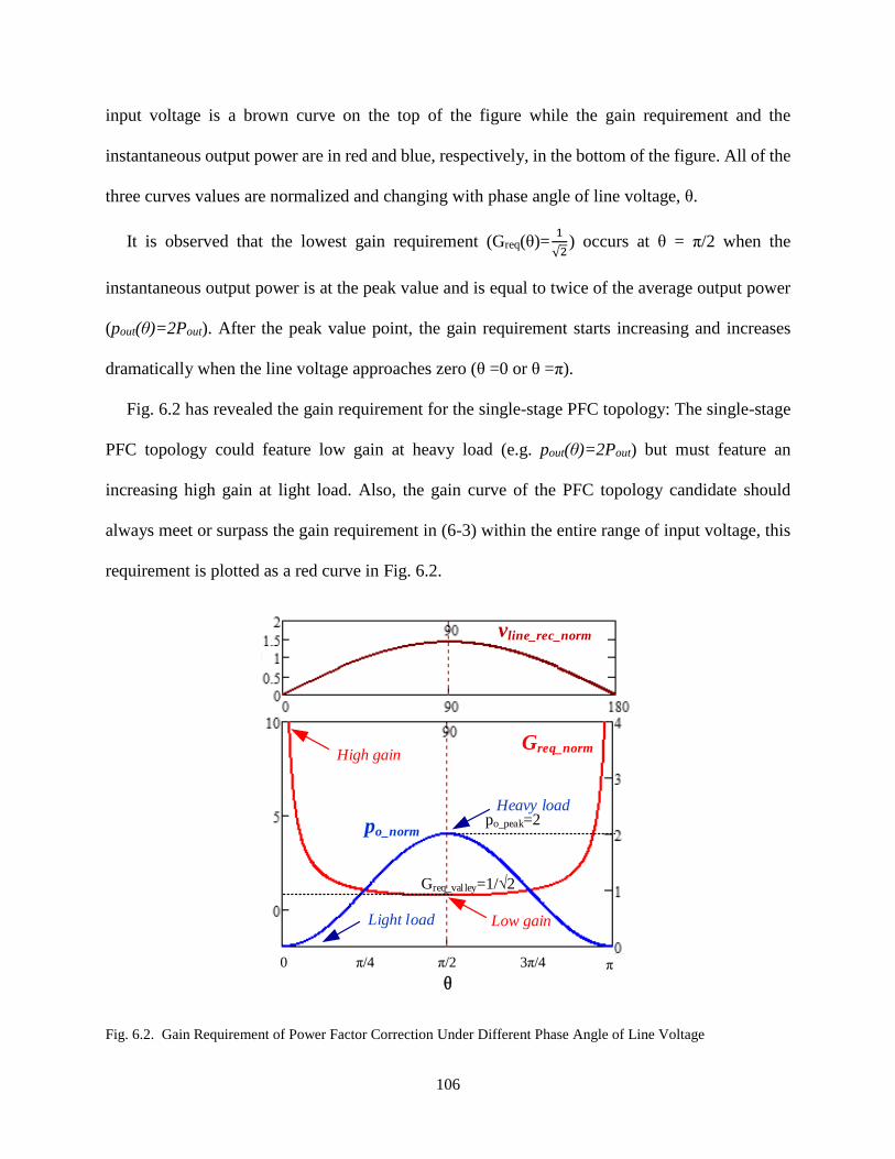
106
input voltage is a brown curve on the top of the figure while the gain requirement and the
instantaneous output power are in red and blue, respectively, in the bottom of the figure. All of the
three curves values are normalized and changing with phase angle of line voltage, θ.
It is observed that the lowest gain requirement (Greq(θ)=1
√2) occurs at θ = π/2 when the
instantaneous output power is at the peak value and is equal to twice of the average output power
(pout(θ)=2Pout). After the peak value point, the gain requirement starts increasing and increases
dramatically when the line voltage approaches zero (θ =0 or θ =π).
Fig. 6.2 has revealed the gain requirement for the single-stage PFC topology: The single-stage
PFC topology could feature low gain at heavy load (e.g. pout(θ)=2Pout) but must feature an
increasing high gain at light load. Also, the gain curve of the PFC topology candidate should
always meet or surpass the gain requirement in (6-3) within the entire range of input voltage, this
requirement is plotted as a red curve in Fig. 6.2.
Heavy load
Low gain
High gain
Light load
vline_rec_norm
po_norm
Greq_norm
θ
po_peak=2
Greq_valley=1/√2
π/2π/4 3π/4 π0
Fig. 6.2. Gain Requirement of Power Factor Correction Under Different Phase Angle of Line Voltage

107
6.3 LLC Resonant Converter Application in Offline High Power LED Driver
The LLC-type series-parallel resonant converter topology has recently become mature and
commercially available in LED driver applications as DC-DC converter because it can achieve
zero voltage switching (ZVS) for the primary side switch and zero current switching (ZCS) for the
secondary side diodes over a wide operating range.
6.3.1 LLC Converter Topology
The schematic of half-bridge LLC resonant converter is shown in Fig. 6.3. The circulating
current is optimized at the nominal input voltage for all load conditions with the narrow frequency
operation range, compared to other resonant topologies, such as series resonant and LCC resonant
topologies. Therefore, this topology is effective in improving efficiency, especially for high-input
voltage applications where the switching loss is more dominant than the conduction loss.
DC
SL
SHLr
Cr
Lm
n:1
D2
D1
Co Io
Vo RL
+
_
Fig. 6.3. Schematic of Half-Bridge LLC Resonant Converter.
Another advantage of LLC resonant converter is the low cost. The series and parallel inductors
could be integrated into the transformer using the leakage and magnetizing inductance, thus the
component count is reduced. Lower voltage-rating output rectifiers can also be used and no
snubber is needed because the output current transition is sinusoidal and, at below-resonance
region, is discontinuous.

108
6.3.2 LLC Application in Conventional Two-Stage Offline High Power LED Driver
In mainstream products of high power LED drivers, LLC resonant converter topology is used
in the second stage of the two-stage AC-DC LED driver configuration to provide galvanic isolation
and output current regulation, as is shown in Fig. 6.4. In this configuration, most of twice-line
frequency pulsing component from AC line input voltage has been filtered by the PFC stage. The
switching frequency range of LLC resonant converter is narrow.
However, the disadvantage of two-stage configuration is that all the power has to be processed
through a PFC stage (Boost Converter is the most popular prototype for PFC stage) first before it
goes into the second stage (LLC converter), which severely sacrifices the total efficiency.
Boost PFC
Converter
LLC Resonant
Converter
vB
Cpfc
Vo
+
_
Rectifier
+
_
LED Lamp
CoAC
Fig. 6.4. Typical LLC Resonant Converter Application in Offline Two-Stage LED Driver.
In this chapter, the LLC is designed to operate in Power Factor Correction (PFC) mode,
rendering a single-stage LED driver solution that combines both of the two functions together
(PFC and output current regulation) into one stage to fully utilize its inherent high-efficiency
feature of the LLC converter. The concept is illustrated in Fig. 6.5. With this topology, all the
power is processed once through the LLC resonant converter and then directly drive the LED lamp.

109
LLC Resonant
Converter
Vo
Rectifier
+
_
LED Lamp
CoAC
Fig. 6.5. Proposed Single-Stage LLC Resonant AC-DC LED Driver.
6.3.3 AC Equivalent Circuit and Output Voltage Gain for LLC Resonant Tank
The LLC series-parallel resonant tank with the equivalent load resistor is illustrated in Fig. 6.6.
This equivalent circuit is widely used to analyze the LLC converter and to calculate the output
voltage gain of LLC resonant tank, MLLC. By using Fundamental Harmonic Approximation (FHA)
method, the series resonant frequency fr, the switching frequency fs, the quality factor Q, the
inductance ratio K, and the output voltage gain MLLC are derived in (6-10) to (6-15), respectively
[54, 55].
vd voeRoeLm
LrCr
Fig. 6.6. AC Equivalent Circuit for LLC Resonant Converter

110
1
2r
r r
fL C
(6-10)
r
r
oe
L
CQ
R
(6-11)
2
2
8oe L
nR R
(6-12)
o
o
L
VI
R (6-13)
m
r
LK
L (6-14)
2 2
2
2
1( )
11 1
LLC s
sr r
s r s
M f
ff fQ
K f f f
(6-15)
2 2
2
1( )
1 1 11 1
LLC s
n
n n
M f
f QK f f
(6-16)
The output voltage gain curves of an LLC resonant tank is plotted in Fig. 6.9 using (6-16),
where fn is the normalized switching frequency (fn=fs/fr).

111
fn=fs/fr
LLC PFC
Operating
Region
fs=fp
Q1=5
Q2=3
Q3=1.6
Q4=1.2
Q5=0.8
Q6=0.6Q7=0.4Q8=0.3
Voltage Gain Plot of LLC Resonant Tank
fs=fr
Fig. 6.7. Voltage Gain Plot of LLC Resonant Converter
Q value is directly proportional to Iout, according to (6-11), (6-12) and (6-13). The LLC tank
gain, MLLC, increases when the Q value decreases, which reflects the load current, Iout, and output
power, pout, reduces.
Since LLC resonant converter features an increasing gain when the load current is decreasing,
this changing trend is in agreement with the gain requirement of PFC operation in 6.2.4. Therefore,
LLC resonant converter is a potential candidate for single-stage PFC operation topology. The
results from (6-10) to (6-15) will be used later to derive the design rule for the LLC converter in
PFC mode.

112
6.4 LLC Resonant Converter Design Rule for Single-stage PFC
The entire LLC PFC design rule is composed of two parts: the transformer turns ratio design
rule and the LLC resonant tank design rule. They will be derived respectively in 6.4.2 and 6.4.3.
The switching frequency range will be defined in 6.4.1 first.
6.4.1 Switching Frequency Range
The total gain of the half-bridge LLC resonant converter, MLLC_total, is expressed as:
_
1
2LLC total LLC sM M f
n (6-17)
Where n is the turns ratio of the transformer (n=Npri/Nsec), MLLC(fs) is the gain of the resonant
tank of the LLC converter, expressed in (6-15).
As can be seen in (6-15), LLC resonant tank has two resonant frequencies: the series resonant
frequency fr, and the parallel resonant frequency, fp. The series resonant frequency, fr, is determined
by Lr and Cr, while the parallel resonant frequency, fp, is determined by Lm+ Lr and Cr.
It is observed that the gain is unity at the series resonant frequency, fr, regardless of the load
variation (Q is cancelled in (6-15) when fs=fr), which is given in (6-18):
2 22
2
1( ) 1
11 1
LLC r
r r r
r r r
M f
f f fQ
K f f f
(6-18)
This is a distinct advantage of LLC-type resonant converter over the conventional series
resonant converter in the high power density and high switching frequency applications such as
LED drivers. It is natural to operate the converter around the resonant frequency to minimize the
switching frequency variation.
The LLC resonant converter can operate at, below or above the series resonance frequency, fr.
Operation below the series resonant frequency allows the soft commutation of the rectifier diodes

113
in the secondary side, while the circulating current is relatively large. Meanwhile, operation above
the series resonant frequency allows the circulating current to be minimized, but the rectifier diodes
are not softly commutated. Therefore, below-resonance operation is preferred for high output
voltage high power applications such as street LED lighting systems where the reverse-recovery
loss in the rectifier diode is severe.
In order to ensure the below-resonance operation and obtain the monotonicity feature of the
converter gain MLLC(fs) over the entire switching frequency range, and make full use of the whole
available below-resonance operation range, we define the operating frequency range of the LLC
PFC in (6-19). The operating area is also shown in the yellow area in Fig. 6.7. The maximum
switching frequency is at the resonant frequency, fr.
p s rf f f (6-19)
This operating area defined in (6-19) has ensured the inductive impedance characteristics of
LLC resonant tank during the operating frequency, so that soft switching can be achieved in both
primary side switches and secondary diodes.
6.4.2 Transformer Turns Ratio Design Rule
According to (6-3), the minimum gain requirement for a PFC design, Greqmin(θ), occurs at θ=π/2
when the input voltage is on its peak value and its instantaneous output power is at the peak and
equal to twice of average output power, which is calculated in (6-20).
min
__
( ) ( )2 22 sin( )
2
out outreq req
in rmsin rms
V VG G
VV
(6-20)
As shown in Fig. 6.7, the minimum gain of the LLC resonant tank in the inductive operating
range occurs at the series resonant frequency, fr.. Therefore, the total gain of the LLC converter at

114
fr is intentionally designed to be equal to the minimum gain requirement of the PFC converter in
(6-20) to make full use of the whole available below-resonance operation range.
According to (6-17) and (6-18), the total gain of LLC resonant converter at the series resonant
frequency fr is derived in (6-21):
In (6-22), the minimum total gain of LLC resonant converter at the series resonant frequency fr
in (6-21) and the minimal gain requirement of PFC in (6-20) is intentionally matched, as follows:
min
_
_
1( )
2 2
outLLC total r req
in rms
VM f G
n V (6-22)
The resulting turns ratio should be designed in (6-23).
_
sec 2
pri in RMS
out
N Vn
N V (6-23)
With the turns ratio design expression in (6-23), the gain requirement at θ=π/2 when the input
voltage is at its peak value (heaviest load) can be satisfied. The later section will derive the LLC
tank design rule to meet the gain requirement during the entire half line cycle, based on the θ-
dependent LLC resonant converter gain expression in PFC mode.
6.4.3 LLC Resonant Tank Design Rule
6.4.3.1 Derivation of Gain Expression of LLC Resonant Converter in PFC mode
The θ-dependent gain expression of LLC resonant converter in PFC mode will be derived first
based on the gain results from (6-10) to (6-15).
Under PFC mode, the equivalent load resistance is no longer a constant value since the input
power is changing with line voltage phase angle, θ. Thus, we need to rewrite the equivalent load
resistance in a θ-dependent form.
_
1 1
2 2LLC total r LLC rM f M f
n n (6-21)

115
According to (6-9), the instantaneous power of LLC converter is derived as
2
2 2
_ _
( ) 2 sin( ) 2 sin( ) oein out
oe full load
Vp P
R (6-24)
Where Roe_full_load is the equivalent LLC converter output resistance when it works at the full
power, Pout. It is expressed in (6-25).
2 2
_ _ _ _2 2
_ _
8 8 ooe full load L full load
o full load
Vn nR R
I (6-25)
Define the equivalent load resistance in PFC mode is Rac. The equivalent circuit of LLC
resonant converter in PFC mode is redrawn in Fig. 6.8.
vd_pfc(θ) voeLm
LrCr
Rac(θ)
Fig. 6.8. AC Equivalent Circuit for LLC Resonant Converter in PFC Mode
Since2
( )( )
oein
ac
Vp
R
and (6-24), the equivalent load resistance in PFC mode can be expressed
as:
2 2_ _
2 22
_ _
( )( ) 2 sin
2 sin( )
oe full loadoe oeac
oein
oe full load
RV VR
Vp
R
(6-26)

116
Derived from (6-11) and (6-12), θ-dependent quality factor under PFC mode, Qpfc(θ), is
rewritten as:
2 2
_
_ _
( ) 2 sin( ) 2 sin( )( )
r r
r r
pfc full load
ac oe full load
L L
C CQ Q
R R
(6-27)
In (6-27), Qfull_load is the full load quality factor when the LLC resonant converter is working at
the full power, Pout, and is a constant value. Its expression is shown in (6-28), according to (6-12)
and (6-13).
2
_ 28
outrfull load
r out
ILQ
n C V
(6-28)
Since the turns ratio has been designed by (6-23), the Qfull_load can be further derived in the
following equation.
22 2
_ 2 2 2
_ __4 4
82
out out out outr r rfull load
r out in RMS r in RMS rin RMS
out
I V I PL L LQ
C V V C V CV
V
(6-29)
LLC resonant tank output voltage gain under PFC mode is obtained by substituting Q with
Qpfc(θ) in (6-15), which is expressed in the following equation:
2 22
2
2 22
4
_2
1( , )
11 1
1
11 1 4 sin
LLC s
sr rpfc
s r s
sr rfull load
s r s
M f
ff fQ
K f f f
ff fQ
K f f f
(6-30)
Then, the total gain expression of LLC resonant converter in PFC mode is shown in (6-31),
according to (6-17).

117
_
2 22
4
_2
1( , ) ( , )
2
1 1
21
1 1 4 sin
LLC total s LLC s
sr rfull load
s r s
M f M fn
nff f
QK f f f
(6-31)
6.4.3.2 Derivation of the Voltage Gain at the Parallel Resonant Frequency of the LLC Resonant
Converter
By calculating the output voltage gain of LLC resonant tank at the parallel resonant frequency,
f=fp, (6-30) comes into a phase-dependent form, given in (6-32).
2 22
4
_2
1( , )
11 1 4 sin
LLC s p
pr rfull load
p r p
M f f
ff fQ
K f f f
(6-32)
The expression can be simplified by using the definition of fp in the following expression:
1
2 ( )p
m r r
fL L C
(6-33)
With the definition of the inductance ratio K in (6-14), the simplified form of LLC resonant
tank voltage gain at the parallel resonant frequency, fp, is shown in (6-34).
2
2 2
_
1( , )
2 sin1
LLC p
full load
M fK
QK
(6-34)
Then, the gain of LLC resonant converter at the parallel resonant frequency, f=fp, is shown in
(6-35), derived from (6-31).
_2
2
_
1 1, ,
22 sin 2
1
LLC total p LLC p
full load
M f M fn K
n QK
(6-35)

118
6.4.3.3 Derivation of the LLC Tank Design Rule
According to (6-3), there is one 1/sinθ item in the expression of single-stage PFC voltage gain
requirement, as shown in (6-36).
_
1( )
sin( )2
outreq
in rms
VG
V
(6-36)
The final expression of the LLC output voltage gain at the parallel resonant frequency, fp, is
derived in (6-37) by substitution the transformer turns ratio expression, n, from (6-23) and the
quality factor expression, Qfull_load, from (6-29) into (6-35) with one 1/(sinθ)2 item in the
expression.
_
22 2
_
2
_
1, ,
2
1 1
2 sin
1 2
LLC total p LLC p
out
in RMSout r
in RMS r
M f M fn
V
VP LK
K V C
(6-37)
Where K is the inductance ratio of magnetizing inductance, Lm, over series resonant inductance
Lr. Pout is the average output power of the PFC converter which is a pre-defined constant.
By comparing both of the expressions in (6-36) and (6-37), it is noticed that, if the LLC resonant
tank gain at the parallel resonant frequency, at θ=π/2 is designed equal to or higher than 1, as
shown in (6-38).
2 2
2
_
1, 1
2
1 2
LLC s p
out r
in RMS r
M f fP LK
K V C
(6-38)
The resulting total LLC resonant converter gain can be derived from (6-37) and is shown in
(6-39).

119
_ 2
_
1,
2 sin
outLLC total p
in RMS
VM f
V
(6-39)
Since the following inequality is always valid for 0≤θ≤π.
2
1 1
sinsin (6-40)
Then the designed LLC converter gain at the parallel resonant frequency, fp, will always meet
or exceed the single-stage PFC gain requirement (0≤θ≤π), as shown in (6-41).
_ 2
_ _
1 1,
sin( )2 2sin
out outLLC total p req
in RMS in rms
V VM f G
V V
(6-41)
In fact, the peak voltage gain frequency, fpeak, where the peak gain is obtained, exists between
fp or fr,
_( , ) ( , )LLC p LLC peak peakM f M f (6-42)
Where p peak rf f f
Thus, the actual switching frequency value during the entire line voltage cycle, fs, will be
between the peak voltage gain frequency, fpeak, and the resonant frequency fr.
p peak s rf f f f (6-43)
In summary, (6-23) and (6-38) are the basic design rules for the LLC resonant converter to
achieve PFC operation with the specified AC input voltage, Vin_RMS, and DC output voltage, Vout:
i. the transformer turns ratio value is designed to be _
2
in RMS
out
V
V or lower.
ii. the gain of the LLC resonant tank at fp is designed to be higher than 1 considering the
case θ=π/2 when line voltage is at peak value.

120
Then the LLC gain will meet the single-stage PFC requirement for all the half line voltage range
(0<θ<π) simultaneously.
6.5 LLC Design Rule for LED Driver Applications
6.5.1 Offline Wide Input and Output Voltages Single-Stage LED Drivers
The LLC PFC design rule is extended in this subsection to explore its applications in the LED
driver design with wide input voltage range and wide output voltage range requirements. Universal
power supplies of LED bars (LED drivers) are typically designed to accept a variable AC line
voltage (e.g. 180VRMS to 300VRMS). In the meantime, customer requires the drivers to produce
a wide output voltage range under the rated output current in order to adept different LED-load
combinations. The ratio of the highest output voltage over the lowest output voltage is usually
1~1.5 times (e.g. VLED=40~60V).
6.5.2 Design Rule for LED Driver Application with Wide Input and Output Voltages
Requirements
It has been already demonstrated that the design of an AC-DC LLC PFC can be simplified into
a design of a LLC converter whose input voltage is equal to the peak input voltage,_2in in rmsv V ,
and whose output power is equal to the peak instantaneous output power of PFC converter,
( ) 2peak outp P .
Considering that the minimum gain requirement of PFC for a wide AC input voltage, Vinmin≤
Vin≤Vinmax, and wide DC output voltage, Vout
min≤Vout≤Voutmax, occurs at the maximum input
(Vinmax) and minimum out (Vout
min), we should set the transformer ratio based on the minimum gain
requirement.

121
The minimum total gain of LLC LED driver at the series resonant frequency, MLLC_driv_total(fr)
is designed to be equal to the minimal gain requirement of designed LLC LED driver, Greq_driv, as
follows:
min
min
_ _ _ max
_
1( )
2 2
outLLC driv total r req driv
driv in rms
VM f G
n V (6-44)
Then, the transformer turns ratio for LLC LED driver, ndriv, should be designed as follows:
max
_max
_
min min
22
2
in rms
in rms
driv
out out
VV
nV V
(6-45)
For the output current-regulated PFC application such as LED driver, the output voltage is
decided by the LED load depending on the number of series-connected LED chips in the LED
lamps, min max
out out outV V V . To explore the design rule of LLC PFC under all the cases of the
output voltage range, we define
max
out outV V (6-46)
min
max1out
out
V
V (6-47)
With the changing of Vout, the gain requirement for wide output voltage range PFC comes into
a λ-related expression. By using (6-46) to replace Vout in (6-3) and considering the lowest AC input
voltage condition, Vin_rmsmin, the gain requirement for wide output voltage range PFC is shown
(6-48).
max
_ min
_
1( , )
sin( )2
outreq driv
in rms
VG
V
(6-48)
According to (6-28) and (6-30), the LLC resonant tank gain is derived as follows:

122
_2 2
2 24
2 2
1( , )
11 1 4 sin
8
LLC driv s
s outr r r
s r s driv r out
M f
f If f L
K f f f n C V
(6-49)
By using (6-46) to replace Vout in (6-49), the LLC resonant tank gain in λ-dependent form is
obtained:
_2 2
2 24
2 2 max
2 22
4 _ _ max
2
2
2
1( , , )
11 1 4 sin
8
1
11 1 4 sin
1
11 1
LLC driv s
s outr r r
s r s driv r out
full load vosr r
s r s
r
s
M f
f If f L
K f f f n C V
Qff f
K f f f
f
K f
2 2
42
_ _ max4 sin s rfull load vo
r s
f fQ
f f
(6-50)
Where Qfull_load_vomax is the quality factor when the output voltage is at Vomax and the output
current is at rated value, Io.
The gain of LLC LED driver resonant tank gain at the parallel resonant frequency, fp, is derived
by using (6-46) to replace Vout in (6-37).
_ _ _
max
2min2 2
min 2
max
2minmax2 2
min 2
1, , , ,
2
1 1
2 sin
1 2 ( )
1 1
2 sin
1 2 ( )
LLC driv total p LLC driv p
driv
out
inout r
in r
out
ino out r
in r
M f M fn
V
VP LK
K V C
V
VV I LK
K V C
(6-51)
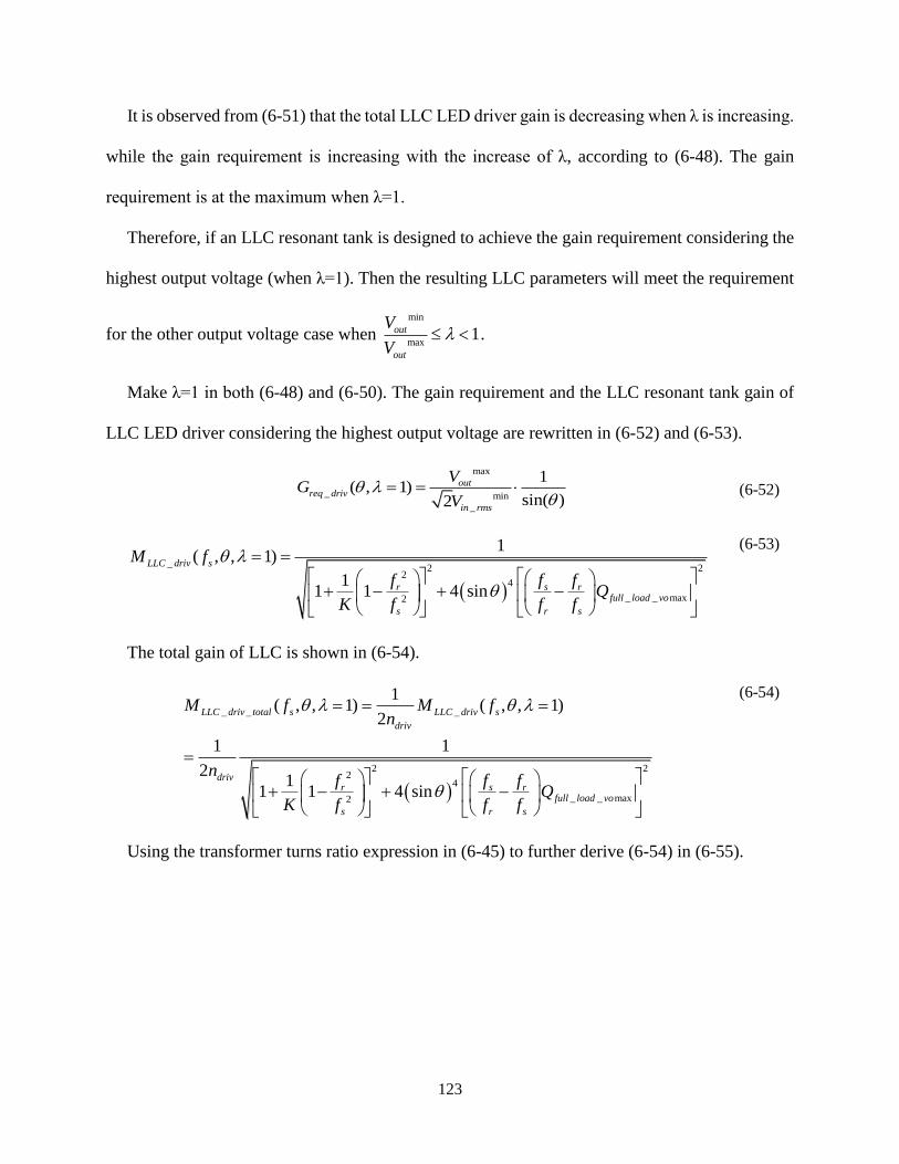
123
It is observed from (6-51) that the total LLC LED driver gain is decreasing when λ is increasing.
while the gain requirement is increasing with the increase of λ, according to (6-48). The gain
requirement is at the maximum when λ=1.
Therefore, if an LLC resonant tank is designed to achieve the gain requirement considering the
highest output voltage (when λ=1). Then the resulting LLC parameters will meet the requirement
for the other output voltage case when min
max1out
out
V
V .
Make λ=1 in both (6-48) and (6-50). The gain requirement and the LLC resonant tank gain of
LLC LED driver considering the highest output voltage are rewritten in (6-52) and (6-53).
max
_ min
_
1( , 1)
sin( )2
outreq driv
in rms
VG
V
(6-52)
_2 2
24
_ _ max2
1( , , 1)
11 1 4 sin
LLC driv s
sr rfull load vo
s r s
M f
ff fQ
K f f f
(6-53)
The total gain of LLC is shown in (6-54).
_ _ _
2 22
4
_ _ max2
1( , , 1) ( , , 1)
2
1 1
21
1 1 4 sin
LLC driv total s LLC driv s
driv
drivsr r
full load vo
s r s
M f M fn
nff f
QK f f f
(6-54)
Using the transformer turns ratio expression in (6-45) to further derive (6-54) in (6-55).

124
_ _ max 2 22_
4min
_ _ max2
min
2 22
4
_ _ max2
1 1( , , 1)
121 1 4 sin2
1
11 1 4 sin
LLC driv total s
in rmssr r
full load voout
s r s
out
insr r
full load vo
s r s
M fV
ff fQV K f f f
V
Vff f
QK f f f
min max_
max max min_ _2
in rms out
rms out in rms
V V
V V
(6-55)
The LLC gain at parallel resonant frequency, fp, is calculated as follows:
_ _
minmin max_
max max min2 22 _ _
4
_ _ max2
22
( , , 1)
1
21
1 1 4 sin
1
sin 21
LLC driv total s p
in rmsout out
in rms out in rmspr r
full load vo
p r p
fu
M f f
VV V
V V Vff f
QK f f f
KQ
K
minmin max_
max max min_ _
_ _ max
minmin max_
2max max min2_ _
_ _ max
2
1 1
2 sin2
1
in rmsout out
in rms out in rms
ll load vo
in rmsout out
in rms out in rms
full load vo
VV V
V V V
VV V
V V VKQ
K
(6-56)
By comparing both of the expressions in (6-52) and (6-56), it is noticed that, if the items in the
bracket on the right side (6-56) is designed equal to or higher than 1, as shown in (6-63).
minmin_
max max2
_
_ _ max
11
21
in rmsout
in rms out
full load vo
VV
V VKQ
K
(6-57)

125
The resulting total LLC LED driver gain at parallel resonant frequency is derived from (6-56)
and (6-57) and is shown in (6-58).
max
_ _ 2min
_
1,
2 sin
outLLC driv total p
in rms
VM f
V
(6-58)
Since the inequality in (6-40) is always valid for 0≤θ≤π. Then the designed LLC LED driver
gain at the parallel resonant frequency, fp, will always meet or exceed the single-stage PFC gain
requirement (0≤θ≤π), as shown in (6-59).
max max
_ _ _2min min
_ _
1 1,
sin( )2 2sin
out outLLC driv total s p req driv
in RMS in rms
V VM f f G
V V
(6-59)
(6-57) can be derived into the LLC resonant converter design rule with wide input and output
voltages, as shown in (6-60).
max max_
_ min min2
_
_ _ max
1,
22
1
in rms outLLC driv s p
in rms out
full load vo
V VM f f
V VKQ
K
(6-60)
In summary, (6-45) and (6-60) show the design rule for the single-stage LLC LED driver with
the wide AC input voltage and DC output voltage:
i. the transformer turns ratio value is designed to be equal to
max
_
min2
in rms
out
V
V
ii. the gain of the LLC resonant tank at fp is higher than the product of the variation ratios
of input voltage and output voltage considering the case θ=π/2 when line voltage is at
peak value.
Then a successful LLC LED driver with wide input and output ranges can be achieved.

126
6.6 LLC PFC Design Example: Single-Stage LLC LED Driver with Wide Input and
Output Voltages
6.6.1 Specifications
The proposed LLC resonant PFC design rule is applied to a 240W half-bridge LLC LED driver
to verify its feasibility and to demonstrate the advantages of the single-stage LLC PFC topology.
The overall design specifications are shown in Table 6.1 with mainstream parameters in products.
Table 6.1. Single-stage LLC LED driver specifications
Vin VLED ILED PO fline
180~300 Vac 40~60 Vdc 4A 240 W 60 Hz
6.6.2 Transformer Turns Ratio Design
Before picking up the LLC resonant tank parameters, the transformer needs to be designed first.
According to (6-45), the transformer turns ratio of the designed half bridge LLC LED driver is
max
_
min
3005.3
2 2 40
in RMS
driv
out
Vn
V
(6-61)
In order to eliminate the overdesigning error of Fundamental Harmonic Assumption and also
simplify the transformer manufacture, the transformer turns ratio value of 5.5 (Np=11 turns and
Ns=2 turns) is chosen in the simulation model as well as the experiment prototype.
6.6.3 LLC Resonant Tank Gain Requirement
For the given set of specifications in Table 6.1, the gain requirements at different input voltage
and output voltage are plotted using (6-48), respectively, shown in Fig. 6.9, where the minimum
gain of each curve occurs at the θ=π/2. It is noticed that the worst case that requires the highest
gain occurs at lowest input voltage and highest output voltage (when λ=1). This curve is plotted in
red in Fig. 6.9.

127
max
_ min
_
( ) 0.236( , )
( ) sin( )2 sin( )
out outreq driv
in in rms
V VG
v V
(6-62)
Fig. 6.9. Gain Requirement Under Different Inputs & Outputs
According to the design criteria for wide input and wide output LLC PFC in (6-60), the product
of the variation ratios of input voltage and output voltage should be calculated first in (6-63) to
define the LLC gain requirement at fp.
max max
min min
300 602.5
180 40
in out
in out
V V
V V (6-63)
Table 6.2 lists the minimum gain requirement value of the desired LLC LED driver under the
given specification in Table 6.1.
Table 6.2. LLC tank gain requirement at the parallel resonant frequency (fp)
MLLC_driv(fp) >2.5
Vout_max 60V
Io_max 4A
Pout=p(θ=π/2)=2Voutmax×Iout 2×60V×4A=480W
According to Table 6.2, we want to achieve an LLC resonant tank design with the gain at the
parallel resonant frequency fp over 2.5 under the output power of 480W.

128
6.6.4 LLC Resonant Tank Design Process
The design method for the above specified LLC PFC is the same as that for conventional LLC
converters, which is available in many literatures [68-72]. The following steps below will lead to
a successful LLC resonant tank design for PFC application.
6.6.4.1 Assumption of Resonant Frequencies fp and fr
Following the design assumption that the designed LLC resonant converter operates in the
below-resonance region to obtain both ZVS on the primary side switches ZCS and secondary side
diodes in LLC resonant converter, fr is the highest switching frequency that provides the unity gain
when input voltage is at the highest peak value (In the case, Vin_pk_max=1.414×300V=424.2V). In
this LED driver design, fr is chosen at 250kHz, which is not only a value within the optimal
switching frequency range of the MOSFETs but also a reasonable frequency that works for the
digital controller and implementation.
Since we have imposed the LLC resonant converter operating within the range of fp~fr, the
design procedure continues with the selection of the parallel resonant frequency, fp, which
determines the maximum current stress and voltage stress for capacitors. It is also assumed that
peak gain of the LLC resonant converter is critically achieved at fp. According to the pre-
determined series resonant frequency, a reasonable parallel resonant frequency of 100 kHz is
chosen, so that the switching frequency variation will be within 100kHz~250kHz.
6.6.4.2 Cr Selection
Once parallel resonant frequency, fp, is selected, the resonant current for minimum peak input
voltage operation (In this case, Vin_pk=1.414×180V=254.5V) can be calculated. At the parallel
resonant switching frequency (fp), theoretically the current in the HB FETs is critically in phase
with the input square-wave voltage. In other words, in half switching cycle, the resonant current

129
will charge the resonant capacitor Cr from its minimum to its maximum voltage [37], [38]. The
charging process is shown in Fig. 6.10.
Qin
VCr_pp
Gate S1 Iresonant Imag
Fig. 6.10. VCr Changing Curve at Minimum Frequency
Thus, given a capacitor value Cr, the voltage stress VCr can be calculated by (6-64) and (6-65),
in which Vin is the input voltage; Qin is the input charge; Po is the average output power; fmin is the
minimum switching frequency; VCr_pk and VCr_pp are the peak value and the peak-to-peak value of
the capacitor voltage. Considering that the maximum peak AC voltage rating for a film capacitor
is around 1kV at 100 kHz, the minimum value of Cr can be obtained. Generally, small Cr value is
preferred to reduce the circulating loss.
(6-64)
(6-65)
_
min
1
2
ohalf cycle in in
PE V Q
f
in_ _
1
2 2Cr pk Cr pp
r
QV V
C

130
6.6.4.3 Lr Selection
Considering the pre-determined resonant frequency (fr=250KHz), once the resonant capacitor
is selected, the resonant inductor can be obtained in (6-66). Large value of Lr is preferred to achieve
the required gain, the magnetizing inductor Lm can be chosen with a large value, which means the
magnetizing current in the primary side is low during the entire input voltage range.
(6-66)
6.6.4.4 Lm Selection
For a given Lr, there is one and only one Lm that pairs with it, to critically achieve the required
parallel resonant frequency gain at minimum input peak voltage (Vin_pk_min=1.414×180V=254.5V
in this case). Thus, Lm can be chosen (103μH in this case). In order to accurately implement the
designed Lm and Lr values in the prototype and simplify the transformer making process, discrete
components are used in the prototype for Lm and Lr.
Considering a reasonable voltage gain margin, the final LLC resonant tank design is shown in
Table 6.3.
Table 6.3. Designed LLC resonant tank parameters
LLC resonant parameter values
Lr 20 μH Lm 103 μH
Cr 20.4 nF
Resonant Frequencies
fr 250 kHz fp 100 kHz
6.6.5 Accurate Switching Frequency Range
It is essential to define the accurate switching frequency to avoid the loss of ZVS in the primary
side switches. The highest frequency is set at the series resonant frequency (fr)
2
1
2r
r r
Lf C
( )

131
max
1 1249.2
2 2 20 20.4r
r r
f f kHzL C H nF
(6-67)
Calculate the parallel resonant frequency (fp) to determine to lowest switching frequency
1 1100.5
2 ( ) 2 (20 103 ) 20.4p
r m r
f kHzL L C H H nF
(6-68)
The switching frequency is limited within the range of 100.5kHz~249.2kHz.
6.7 Mathematical Verification
Based on the designed LLC resonant tank parameters, the voltage gain of the LLC tank are
calculated using the mathematic software, Mathcad, with which the feasibility of the LLC PFC
(LLC LED driver) design rule is verified mathematically in this section.
6.7.1 Normalized Gain Curves of the Designed LLC PFC at Typical Loads
Fig. 6.11 shows the normalized gain curve of the designed LLC resonant tank at the heaviest
load when θ=π/2. Fig. 6.12 shows the gain curves under the loads at some typical line voltage
phase angle : θ=90˚, θ=60˚, θ=45˚, θ=30˚.
From Fig. 6.12, the changing trend of the gain curve is understood: With the decrease of the
phase angle of line voltage, θ, the load is decreasing corresponding to the decreased Q value, while
the gain is increasing. This meets the changing trend requirement of the single-stage PFC converter
in 6.2.4.

132
Fig. 6.11. Normalized Gain Plot of the Designed LLC Resonant Converter at heaviest load pO(θ=π/2)=2PO
0.2 0.29 0.38 0.47 0.56 0.65 0.74 0.83 0.92 1.01 1.10
2
4
6
8
10
12
14
16
18
20
Normalized Gain Plot for LLC Resonant Converter
M fn Q_90_deg
M fn Q_60_deg
M fn Q_45_deg
M fn Q_30_deg
M fn Q_20_deg
fn
Gain M
Q (Load)
Fig. 6.12. Normalized Gain Plot of the Designed LLC Resonant Converter at other typical loads

133
6.7.2 LLC PFC design rule verification under Vout=Voutmax
Also, it is noticed in Fig. 6.11 that the designed LLC resonant tank features a normalized gain
of 2.72 at the parallel resonant frequency fp/fr=0.392, which is higher than the requirement of 2.5
by 9%. According to the proposed design rule of LLC LED driver in (6-60), the LLC gain will
meet the requirement for the entire line voltage phase angle (0<θ<π) simultaneously.
This has been proved in Fig. 6.13, where both the achieved gain curve of the designed LLC
converter and the PFC gain requirement curve are plotted using the mathematic software, based
on the specifications in Table 6.1 and the designed LLC resonant tank parameters in Table 6.3.
The gain curve of the designed LLC PFC crosses the gain requirement only at θ=π/2, and then is
always higher than the PFC gain requirement over the entire line voltage cycle.
π/4 3π/4
θ
π/4 3π/4π/2 π0
π/2 π0
Greq_driv(π/2)=MLLC_driv_total(π/2)
vline_rec_norm(θ)
Greq_driv(θ)
po_norm(θ)
MLLC_driv_total(θ)
Fig. 6.13. Gain Requirement and Gain Curve of the Designed LLC Resonant Converter Considering the Highest
Output Voltage (Vout=Voutmax)

134
6.7.3 LLC PFC design rule verification considering the entire output voltage range
Considering the entire operating range of output voltage, a 3-D surface plot is drawn in Fig.
6.14 using the PFC gain requirement expression in (6-62) and the LLC gain expression at
paralleled resonant frequency in (6-51). The gain requirement is a red surface, while the LLC gain
is an irregular colored surface. Both of them are changing with λ=Vo/Vomax and phase of line voltage
θ. It is observed that the designed LLC resonant tank features the gain that is always higher than
the requirement within the specified output voltage range as well as the entire half line voltage
cycle (0.667<λ<1, 0˚<θ<180˚), resulting in a successful LLC PFC design.
MLLC_driv_total Greq_driv MLLC_driv_total Greq_driv
Greq_driv(θ,λ)
MLLC_driv_total(θ,λ )
MLLC_driv_total(θ,λ )
Greq_driv(θ,λ)
Fig. 6.14. Designed LLC Resonant Converter Gain & PFC Gain Requirement in 3D Surface Plot
Considering the Wide Output Voltage (Voutmin<Vout<Vout
max)

135
6.8 Simulation Verification
In 6.6, the LLC design rule for PFC application is applied to a wide input voltage and wide
output voltage range LED driver as an example. As a result, the LLC resonant tank parameters are
designed and meet the gain requirement of the specified constant output current LED driver
application.
6.8.1 LLC PFC LED Driver Architecture and Simulation Model in PSIM
The designed LLC PFC LED driver architecture is shown in Fig. 6.15.
SL
SHLr
Cr
LmD2
Co
ILED+
_
LFB
CFB
Q1 Q2
Q3 Q4
CauxNs2
Daux
+
_
VLED
T
vin
D1 D2
D4D3
Full-Bridge Ripple Cancellation Converter
D1
Bridge Rectifier Single-Stage Half-Bridge LLC PFC Converter
Fig. 6.15. Proposed Single-Stage LLC PFC LED Driver Architecture with Full-Bridge Ripple Cancellation Converter
In order to achieve a not only high power efficiency but also flicker-free offline LED driver,
the driver architecture is composed of two parts: the single-stage half-bridge LLC PFC converter
and full-bridge bipolar ripple cancellation converter. The single-stage LLC PFC converter is in
charge of achieving high power factor and providing high efficiency AC-DC single-stage power
conversion solution while the full-bridge bipolar ripple cancellation converter is to remove the low
frequency AC ripple in the LED current.
A complete simulation model of the LED driver is built in circuit simulation software, PSIM,
as shown in Fig. 6.16. The LLC PFC stage is composed of two parts: the power train and the
controller. The power train elements in the LLC PFC converter are the same as the conventional
LLC DC-DC resonant converter, including a bridge rectifier, LLC resonant tank and a center-

136
tapped rectifier on the secondary side. In the LLC PFC control part, three items are sensed in order
to operate the LLC topology in PFC mode: rectified AC input voltage, input current and output
current (output current is regulated in LED driver application). The input voltage is sensed and
scaled by the voltage divider before it becomes the reference of the average input current. The
output current is sensed with a resistor connected in series with the LED bulbs and the information
is transmitted to the primary side. The average input current is the third control parameter. Actually,
it is a critical controlled objective in power factor correction. However, it is difficult to accurately
obtain the average input current over one switching cycle (by a series-connected current sensing
resister) in LLC resonant topologies due to the irregular current waveform and the existence of
circulation current. In the simulation, a cycle-by-cycle average input current sensing method [71]
is used for LLC resonant converter. It utilizes the series resonant capacitor voltage to derive the
average input current, thus is lossless, accurate, and low-cost. The detailed control strategy will be
discussed in Section 6.9.1.
In the meantime, a full-bridge ripple cancellation stage control is applied to eliminate the double
line frequency current ripple in output current caused by the PFC operation.

137
Fig. 6.16. Proposed Single-Stage LLC PFC LED Driver Simulation Model in PSIM.

138
The power train parameters of the simulation model are shown in Table 6.4.
Table 6.4. Key parameters in single-stage LLC LED driver simulation model
LLC PFC Converter
Transformer turns ratio
Npri:Nsec1 11:2
Transformer magnitizing
inductance (Lm) 103µH
Series inductance (Ls) 20 µH
Series Capacitor (Cs) 20.4 µF
Output capacitor 1000µF×3
Switching frequency(fsw) 100 to 250kHz
Full-bridge Bipolar Ripple Cancellation Converter
Transformer turn's
ratioNsec1:Nsec2 2:1
RCC input capacitor (Caux) 470µF
RCC output capacitor (CFB) 4.7µF
6.8.2 Power Factor Correction Performance
To demonstrate the power factor correction performance of LLC LED driver, the
waveforms of input voltage and input current under two critical gain requirements: case 1
(highest input voltage (300Vac) and lowest output voltage (40V)) and case 2 (lowest input
voltge (180Vac) and highest output voltage (60V)) are given in Fig. 6.17 and Fig. 6.18.
It is observed that the designed LLC PFC stage has achieved high power factor (PF>0.99)
in both cases. It is also noted that the minimum switching frequency occurs at the highest
gain requirement near the current passing zeros. The maximum switching frequency occurs
at the lowest gain requirement when AC input voltage is at the peak value. It can be noted
from Fig. 6.11 that the objective gain 2.5 is achieved at 116kHz, meaning that the LLC
resonant converter will operating at 116kHz when Vin_rms=180V and Vout=60V. This has
been verified in the simulation in Fig. 6.17 (b).

139
Input Voltage: 180Vac
PF=0.995
Input Current
(a) Input voltage (vacin) & input current (iin) waveforms of LLC PFC (PF=0.995) at Vin_RMS =180V
Io=4A out Vout=60V
Operating Frequency:100.5KHz~116KHz
PF=0.995
Input Current
116KHz100.5KHz
(b) Input current (iin) & switching frequency (Fs) waveforms at Vin_rms =180V Io=4A out Vout=60V
Fig. 6.17. Simulation Results of LLC PFC in Case 1 (Resonant Tank Parameters: Lm=103µH Lr=20µH
Cr=20.4nF)

140
Input Voltage: 300Vac
PF=0.994Input Current
(a) Input voltage (vacin) & input current (iin) waveforms of LLC PFC working at Vin_rms =300V Io=4A
out Vout=40V
PF=0.994Input Current
Operating Frequency:100.5KHz~220KHz
220KHz100.5KHz
(b) Input current (iin) & switching frequency (Fs) waveforms working at Vin_rms =300V Io=4A
Vout=40V
Fig. 6.18. Simulation Results of LLC PFC in Case 2 (Resonant Tank Parameters: Lm=103µH Lr=20µH
Cr=20.4nF)

141
6.8.3 Ripple Cancellation Performance
The designed LLC LED driver is simulated under different cases that are specified in
Table 6.1. In Fig. 6.19, the simulated waveforms of the LLC PFC converter output voltage,
Vo_LLC, the bipolar cancellation converter output voltage, Vinv, the LED voltage, VLED, and
the LED current, ILED, are given under two typical cases: i. VLED=60V Vin_RMS=180VRMS
ILED=4A and ii. VLED=40V vacin=300VRMS ILED=4A.
4.5V pk-pk
4.5V pk-pk
0.4V pk-pk
0.2A pk-pk
LLC output voltage
RCC output voltage
LED voltage
LED current
(a) Lowest Gain under lowest input voltage (180VRMS) and highest output voltage (60Vdc)

142
4.5V pk-pk
4.5V pk-pk
0.4V pk-pk
0.2A pk-pk
LLC output voltage
RCC output voltage
LED voltage
LED current
(b) Highest Gain under highest input voltage (300VRMS) and lowest output voltage (40Vdc)
Fig. 6.19. Bipolar Ripple Cancellation Performance in Simulation in Two Typical Cases when Iout=ILED=4A
(Resonant Tank Parameters: Lm=103µH Lr=20µH Cr=20.4nF)
As shown in Fig. 6.19, the bipolar ripple cancellation converter generates an out-of-
phase AC voltage (Vinv) to cancel the AC ripple in the LLC PFC converter voltage (Vo_LLC),
enable the sum of these two output voltages (VLED) to be ripple-free. This DC voltage (VLED)
goes across the LED bulbs and results a ripple-free LED current (ILED). With the LED
current ripples (Iripple_pk-pk=0.2A, Iripple@120Hz=0.1A) in both cases less than 2.5% of
nominal LED current (ILED=4A), the light flicker caused by the low frequency AC LED
current ripple is eliminated.

143
6.9 Experimental Verification
Following the simulation model in Fig. 6.16, a prototype is built to verify the
performance of the designed LLC LED driver. Correspondent to the simulation model in
Fig. 6.16, the prototype is also divided into two parts: the single-stage LLC PFC and full-
bridge bipolar ripple cancellation converter.
In the prototype, bipolar ripple cancellation converter is implemented by analog
Sinusoidal Pulse Width Modulation (SPWM) to achieve flicker-free operation. Since the
bipolar ripple cancellation technology has been introduced in Chapter 3, the detail design
steps have been given in section 3.3.
Power factor correction of the designed LLC resonant converter is implemented using
a digital controller, which is discussed in the following subsection in details.
6.9.1 Digital Implementation of LLC PFC Control
As shown in Fig. 6.20, a Microchip DSC dsPIC33FJ32GS606 is used to implement the
digital controller. A linear opto-coupler is used to transmit LED current signal to the
primary side. The LED current signal is sampled by an ADC, and then subtracted from a
reference voltage value to create an error value. The error value is processed by a slow PI
controller and becomes one of the two essential signals to create the input current reference.
The other essential information for the input current reference is the sinusoidal input
voltage. The rectified input voltage is firstly scaled down to adapt the DSC analog input
range and then sampled by the second ADC. By multiplying the error value from the first
ADC and the scaled input voltage reference from the second ADC, a rectified sinusoidal
input current reference signal is generated.

144
Since it is difficult to accurately obtain the average input current value over one
switching cycle in LLC resonant topology due to the irregular current waveform and the
existence of circulation current, the input current value is calculated by using the cycle-by-
cycle average input current sensing method proposed in [71]. This method accurately
measures the average input current over each switching period by sensing the series
resonant capacitor voltage and the input voltage at a particular time instant and thus
provides real-time average input current information.
Input Current Sensing Algorithm
ii
Cr Cj
Optional
Parametersfs
Scale
down
Scale
down
Current
sensing
Linear Opto- coupler and
Peripheral CircuitryPI +_
ILED_ref
PI+_
Gate
Drivers
tHoff & tLoffS/H
Switching
Period
complementary signals
at 50% duty cycle
Internal
CounterComparator
Digital Signal Controller
vi
vCs
Multiplier
vi
ILED_sens
SH SL
Control signal
Generator
AD
C
ADCADC
SL
SH Lr
20uH
Cr
20.4nF
Lm
103uHD2
Co
3mF
ILED 4A
+
_
LFB
22uH
CFB
4.7uF
Q1 Q2
Q3 Q4
Caux
470uFNs2
Daux
+
_
VLED
40~60V
T
vin
D1 D2
D4D3
Full-Bridge Ripple Cancellation Converter
D1
Bridge Rectifier Single-Stage Half-Bridge LLC PFC Converter
Analog Implementation
of Bipolar Ripple
Cancellation Control
Full Bridge MOSFETs
Drivers
SPWM signals to Q1 ~ Q4
180~300
Vac
Fig. 6.20. The Implementation of the Proposed Single-Stage LLC Resonant LED Driver.
The average input current over one switching period is expressed in the following
equation:
( ) ( ) 2
in net s
r s Cs Hoff Cs Loff j s in
I Q f
C f v t v t C f V
(6-69)

145
Where Cr is the resonant capacitance, fs is the switching frequency of LLC converter
primary-side switches, tHoff the high-side switch’s turn-off point and tLoff is the low-side
switch’s turn-off points, vCs is the voltage across the resonant capacitor, Cj is the MOSFET
junction capacitance, Vin is the input voltage of the LLC tank.
It can be observed from (6-69) that once the series resonant capacitor voltage at the
high-side and the low-side switches’ turn-off points are measured, the average input current
over that switching period can be calculated, if switching frequency, resonant capacitance,
MOSFET junction capacitance and input voltage information are available.
In order to catch the series resonant capacitor voltage information at switches’ turn-off
points, the third ADC is used, whose sample & hold time instant is accurately synchronized
with the control signal generator. The calculating result of input current signal is subtracted
from the input current reference signal to create an error value. This error value is processed
by a fast PI controller to recalculate and adjust the switching period.
The switching period value is then compared with the build-in counter in the DSC to
generate a pair of complementary switching signals working at the constant duty cycle of
50%. In the meantime, a dead time is added between the two complementary switching
signals to avoid the short through of the power source. The two power switches in half-
bridge LLC converter are controlled by the pair of complementary switching signals
through the gate drivers. By adjusting the switching period of LLC resonant converter, the
input current is controlled and forced to follow the input voltage and thus a high power
factor is achieved.
The key circuit components and parameters of the experimental prototype are listed in
the following table.

146
Table 6.5. Key circuit components and parameters in LLC LED driver prototype
Overall LED Driver
Input voltage range 180Vrms to 300Vrms
Output voltage 40 to 60VDC
Output current Up to 4ADC
Half-bridge LLC PFC
Transformer turns ratio
Npri:Nsec1 11:2
Transformer Core PQ 40
Transformer magnitizing
inductance (Lm) 103µH
External Series Inductor
(Lr) 20 µH
Series Resonant Capacitor
(Cr) FKP1O116804D00JSSD×3 (6800pF 1KV)
Primary-side Switches STB34N50DM2AG×2 (500V, 26A)
Secondary-side Output
diodes STPS30170DJF-TR×4 (170V, 30A)
PFC stage Output
Capacitor B43504A2108M×3
(1000µF, 250V)
Digital Controller Microchip DSC dsPIC33FJ32GS606
Full-bridge Bipolar Ripple Cancellation Converter
Transformer turn's ratio
Nsec1:Nsec2 2:1
Switching Frequency 156KHz
Full-bridge switches FDS6900AS×2 (Dual N-Ch MOSFETs
30V, 7.5A)
MOSFETs driver NCP3420×2
Inductor 74435582200 (22µH, 15A, 7mOhm)
RCC input capacitor EEU-FR1E471YB (470 µF, 25V)
RCC output capacitor C0805C475K4PACTU (4.7 µF, 16V)
SPWM controller MC33060A
LED Load Section
LED load
2 branches of 18 pieces series-connected
LEDs chips to produce 60V 4A LED load
PN: XMLBWT-02-0000-0000T5051CT

147
6.9.2 Power Factor Correction Performance
The waveforms of input voltage and input current are measured and four typical cases
are shown in Fig. 6.21. The designed LLC PFC LED driver achieves a peak power factor
of 0.99 at Vin=180Vac while keeps over 0.97 under nominal input, Vin=220Vac and full
load, Po=240W. More power factor performance data under different cases is shown in Fig.
6.22.
Input Voltage: 180Vac
PF=0.99
Output Current: 4Adc
Input Current
Input Voltage: 220Vac
PF=0.97
Output Current: 4Adc
Input Current
(a) Vin=180Vac, VLED≈60V, ILED=4A, PO=240W (b) Vin=220Vac, VLED≈60V, ILED=4A, PO=240W,
Input Voltage: 180Vac
PF=0.925
Output Current: 4Adc
Input Current
Input Voltage: 220Vac
PF=0.90
Output Current: 4Adc
Input Current
(c) Vin=180Vac, VLED≈40V, ILED=4A, PO=160W (d) Vin=220Vac, VLED≈40V, ILED=4A, PO=160W
CH1: Rectified AC input voltage (vin: 250V/div) CH2: AC input current (iin: 2A/div)
CH3: LED lamp current (ILED: 2A/div)
Fig. 6.21. Input Voltage, Input Current and Output Voltage of the Designed Single-stage LLC LED Driver

148
Fig. 6.22. Power Factor Performance of LLC PFC LED Driver When VLED≈40~60V, ILED=4A.
It is noticed that there are “a blank portion” of input current in the vicinity of the input
voltage zero crossing points. And the lower input current (Iin_rms) the LLC PFC operates at,
the longer “blank portion” is.
This is caused by the nonlinearity of the MOSFET junction capacitance, Cj. According
to the input current sensing expression in (6-69), the input current is composed of two
portions: the resonant current going across the series resonant capacitance, Cr and the
energy input charge resulted from the junction capacitances, Cj. Among these two items,
the contribution from the junction capacitor Cj becomes dominant when the LLC is
operating at the light load.
The value of Cj includes output capacitance of the MOSFET, Coss, and any capacitance
in parallel with the MOSFET drain-to-source nodes. Coss is a nonlinear capacitance that
varies with the drain-to-source voltage of the MOSFET. A charge-equivalent linear
capacitance can be derived from datasheet, which is the average value of the Coss–VDS curve
from 0V to Vin [73]. However, the equivalent Cj is different at different input voltage. As
0.920.90
0.78
0.950.93
0.82
0.990.97
0.90
0.7
0.75
0.8
0.85
0.9
0.95
1
180V 220V 300V
LLC PFC+FB RCC PF (Io=4A)
40V output 50V output 60V output

149
a constant Cj value is used in the existing digital implementation, the nonlinearity of Cj
value in the real circuit results the sensing error at the light input current and the low input
voltage. As the input current value in the vicinity of the input voltage zero crossing points
is overestimated, the controller cannot force the input current curve completely follow the
input voltage. This blank portion disappears when input voltage keeps increasing until the
impact of Cj item becomes minor and the Cr item dominates the input current measurement
result in (6-69). Nevertheless, the power factor performance at nominal input voltage and
full load (Vin=220Vac, Po=240W) is still higher than 0.97, which passes the Energy Star
program power factor (PF) requirements (PF=0.9) for solid state lighting luminaires with
large margin.
6.9.3 Soft Switching Performance
Because the low-side switch, SL, and the high-side switch, SH, are symmetrically located
beside the LLC resonant tank and the driving signals are complementary, both of the low-
side switch, SL, and the high-side switch, SH, experience the same switching process but
have the complementary switching waveforms. To simplify the analysis, only operation of
the low-side switch in LLC resonant is studied in Fig. 6.23, where Fig. 6.23 (a) presents
the waveforms of input voltage, drain-to-source voltage of the low-side switch and gate
driving signal of the low-side switch during a 1/4 line voltage cycle (0˚≤θ≤90˚). In this
case, input voltage is 180VRMS, output voltage is 60V, while output current is 4A. Fig.
6.23 (b~g) show the zoomed-in waveforms under the following typical six phases Fig. 6.23
(b) for θ=0˚Fig. 6.23 (c) for θ=20˚; Fig. 6.23 (d) for θ=30˚; Fig. 6.23 (e) for θ=45˚; Fig.
6.23 (f) for θ=60˚; Fig. 6.23 (g) for θ=90˚.

150
Case 6: θ=90˚
Case 5: θ=60˚
Case 4: θ=45˚
Case 3: θ=30˚
Case 2: θ=20˚
Case 1: θ=0˚
(a) The whole waveforms of input voltage, drain to source voltage and gate driving signal of low-
side switch under different phase angle (0˚≤ θ ≤90˚)
Ch4: Gate Driving signals
Ch3: Drain to Source Voltage
Ch1: Input Voltage= 16V
Zero Voltage Switching
Case 1: θ=0˚
Ch4: Gate Driving Signal
Ch3: Drain to Source Voltage
Ch1: Input Voltage= 92V
Zero Voltage Switching
Case 2: θ=20˚
(b) Case 1: θ =0˚ (c) Case 2: θ =20˚
Ch4: Gate Driving signalsCh3: Drain to
Source Voltage
Ch1: Input Voltage= 136V
Zero Voltage Switching
Case 3: θ=30˚
Ch4: Gate Driving signals
Ch3: Drain to Source Voltage
Ch1: Input Voltage= 180V
Zero Voltage Switching
Case 4: θ=45˚
(d) Case 3: θ =30˚ (e) Case 4: θ =45˚
Ch4: Gate Driving signals
Ch3: Drain to Source Voltage
Ch1: Input Voltage= 220V
Zero Voltage Switching
Case 5: θ=60˚
Ch4: Gate Driving signals
Ch3: Drain to Source Voltage
Ch1: Input Voltage= 248V
Zero Voltage Switching
Case 6: θ=90˚
(f) Case 5: θ =60˚ (g) Case 6: θ =90˚ CH1: Rectified AC input voltage (vin: 100V/div) CH3: Drain to source voltage (Vds: 50V/div) CH4: Gate
driving signal (Vgs: 5V/div)
Fig. 6.23. Soft Switching Performance of the LLC PFC Stage on Primary Side at Different Phase
Angle, When Vin=180Vac, VLED≈60V, ILED=4A, PO=240W

151
Since the designed converter is working in below-resonance region, the main switches
in LLC topology are always softly commutated. As illustrated in the Fig. 6.23 (b~g), the
gate driving signal always step up after the drain-to-source voltage drops down to zero
volts (or close to zero volts) during the entire half line cycle when the input voltage
increases from the valley voltage (16V) to peak voltage (248V). As a result, the turning on
loss on the switches is eliminated, and the efficiency is improved.
In order to investigate the soft switching operation on the secondary side, the resonant
current through the LLC resonant tank is measured, when input voltage is 180VRMS,
output voltage is 60V, while output current is 4A. Fig. 6.24 shows the the zoomed-in
waveforms under the following typical six phases Fig. 6.24 (b) for θ=0˚ Fig. 6.24 (c) for
θ=20˚; Fig. 6.24 (d) for θ=30˚; Fig. 6.24 (e) for θ=45˚; Fig. 6.24 (f) for θ=60˚; Fig. 6.24 (g)
for θ=90˚. In the six zoomed-in figures, the resonant current is measured in CH4 and is a
sinusoidal curve composed of two parts: the first part is a triangle waveform representing
the current going through the magnetizing inductor and the second part is the current
transmitted to the load through the secondary side diodes. As the switching frequency is
below the resonant frequency fr, the secondary side diodes satisfy the ZCS condition. It is
observed that there is no current spike on CH4 curves at the switching point, which means
the current through the diodes always decrease to zero each switching cycle during the
entire half line cycle, reduce the turning off loss on the devices.

152
Ch1: Input Voltage: 180Vac
Case 6: θ=90˚
Case 5: θ=60˚
Case 4: θ=45˚
Case 3: θ=30˚
Case 2: θ=20˚
Case 1: θ=0˚
(a) The whole waveforms of input voltage, resonant current and gate driving signals under
different phase angle (0˚≤ θ ≤90˚)
Ch2: High side driving signalCh3: Low side driving signal
Ch1: Input Voltage= 16V
Case 1: θ=0˚
Ch4:Resonant current
Ch2: High side driving signalCh3: Low side driving signal
Ch1: Input Voltage= 81V
Case 2: θ=20˚
Ch4:Resonant current
(b) Case 1: θ =0˚ (c) Case 2: θ =20˚
Ch2: High side driving signalCh3: Low side driving signal
Ch1: Input Voltage= 113V
Case 3: θ=30˚
Ch4:Resonant current
Ch2: High side driving signalCh3: Low side driving signal
Ch1: Input Voltage= 163V
Case 4: θ=45˚
Ch4:Resonant current
(d) Case 3: θ =30˚ (e) Case 4: θ =45˚
Ch2: High side driving signalCh3: Low side driving signal
Ch1: Input Voltage= 224V
Case 5: θ=60˚
Ch4:Resonant current
Ch2: High side driving signalCh3: Low side driving signal
Ch1: Input Voltage= 272V
Case 6: θ=90˚
Ch4:Resonant current
(f) Case 5: θ =60˚ (g) Case 6: θ =90˚
CH1: Rectified AC input voltage (vin: 100V/div) CH2: High side gate driving signal (Vgs_h: 5V/div) CH3:
Low side gate driving signal (Vgs_l: 5V/div) CH4: Resonant current (ires: 5A/div)
Fig. 6.24. Soft Switching Performance of the LLC PFC Stage on Secondary Side at Different Phase
Angle, When Vin=180Vac, VLED≈60V, ILED=4A, PO=240W

153
6.9.1 Efficiency Performance
With the help of soft switching operation in both primary and secondary side, the
switching loss of LLC resonant converter is significantly reduced. The efficiency mainly
depends on the conduction loss caused by the resonant current. In fact, the efficiency under
the fixed load (when output voltage, VLED, and output current, ILED, are fixed) increases
when the input voltage is increasing. This is because the resonant current of LLC
converter’s efficiency is optimized at resonant frequency (fr) when the resonant current is
minimized, according to the LLC resonant converter resonant tank feature. Because the
LLC converter has been designed to work in the below-resonance region, the resonant
frequency, fr, is the highest switching frequency. The higher the input voltage is, the lower
output gain is required and the closer the switching frequency is from the resonant
frequency, fr. As a result, the conduction loss is reduced when the input voltage is at the
highest. This has been verified in the experimental results.
The prototype is tested in three typical output voltage cases: 40V, 50V and 60V while
the input voltage is changing from the lowest specified AC input voltage (180VRMS) to
the highest (300VRMS). All the cases are tested under the same output current (ILED=4A).
The experimental results show the power conversion efficiency of single-stage LLC PFC
has exceeded 91.3% at nominal input (220VRMS). The peak efficiency is 92%.
Considering the loss on winding-connected ripple cancellation converter, the power
conversion efficiency is still over 90% at nominal input voltage (220VRMS). The peak
efficiency of the system is 90.8%.

154
(a) Single-stage LLC PFC Efficiency
(b) LLC PFC LED Driver Efficiency with Bipolar Ripple Cancellation Converter
Fig. 6.25. LLC PFC LED Driver Efficiency Performance under Different Input Voltage
90.7%
91.3%
91.8%
90.8%
91.4%
92.0%
90.2%
90.7%
91.1%
88.0%
88.5%
89.0%
89.5%
90.0%
90.5%
91.0%
91.5%
92.0%
180V 220V 300V
LLC PFC eff (Io=4A)
40V output 50V output 60V output
89.5%
90.1% 90.5%
89.6%
90.4%
90.8%
89.4%
89.9%90.2%
88.0%
88.5%
89.0%
89.5%
90.0%
90.5%
91.0%
91.5%
92.0%
180V 220V 300V
LLC PFC+FB RCC eff (Io=4A)
40V output 50V output 60V output

155
6.9.2 Ripple Cancellation Performance
A bipolar ripple cancellation converter has been added to the single-stage LLC PFC
stage to remove the double line frequency ripple in LED current, as shown in Fig. 6.20.
The bipolar ripple cancellation performance is shown Fig. 6.26, where CH1: LLC PFC
output voltage (CH1: vLLC, 5V/div), bipolar RCC output voltage (CH2: vRCC, 5V/div), LED
voltage (CH3: vLED, 5V/div) and LED current (CH4: iLED, 200mA/div) are measured. The
LLC LED driver prototype is tested at the rated current of 4A under different operating
conditions as follows: (a) Vin=180Vac, VLED≈60V, ILED=4A, PO=240W (b) Vin=180Vac,
VLED≈50V, ILED=4A, PO=200W (c) Vin=180Vac, VLED≈40V, ILED=4A, PO=160W (d)
Vin=220Vac, VLED ≈ 60V, ILED=4A, PO=240W (e) Vin=220Vac, VLED ≈ 50V, ILED=4A,
PO=200W (f) Vin=220Vac, VLED≈40V, ILED=4A, PO=160W. In order to investigate the
double line frequency ripple component, LLC output voltage, LED voltage and LED
current are measured in AC coupled mode where the DC components have been removed
before displaying on the scope.
It is observed that the 5V peak-to-peak double line frequency AC ripple in LED voltage
(as shown in CH1), is cancelled by an out-of-phase 5V peak-to-peak AC voltage from
bipolar RCC (CH2), resulting a flat DC voltage (CH3) across the LED lamp. As a result,
the current through the LED lamp is also a flat DC value (CH4) and generate flicker-free
lumen outputs. The double line frequency (120Hz) current ripple is significantly reduced
after the bipolar ripple cancellation, which is generally smaller than 13mA (0.325% of the
average LED current).

156
LLC PFC output voltage
RCC output voltageLED voltage
LED current
5V pk-pk
5V pk-pk
ILED@ 120Hz=4mA
LLC PFC output voltage
RCC output voltageLED voltage
LED current
5V pk-pk
5V pk-pk
ILED@ 120Hz=4.5mA
(a) Vin=180Vac, VLED≈60V, ILED=4A, PO=240W (b) Vin=180Vac, VLED≈50V, ILED=4A, PO=200W
LLC PFC output voltage
RCC output voltageLED voltage
LED current
5V pk-pk
5V pk-pk
ILED@ 120Hz=12mA
LLC PFC output voltage
RCC output voltage LED voltage
LED current
6.5V pk-pk
ILED@ 120Hz=6mA
6.5V pk-pk
(c) Vin=180Vac, VLED≈40V, ILED=4A, PO=160W (d) Vin=220Vac, VLED≈60V, ILED=4A, PO=240W
LLC PFC output voltage
RCC output voltage LED voltage
LED current
6.5V pk-pk
ILED@ 120Hz=8mA
6.5V pk-pk
LLC PFC output voltage
RCC output voltage LED voltage
LED current
6.5V pk-pk
ILED@ 120Hz=13mA
6.5V pk-pk
(e) Vin=220Vac, VLED≈50V, ILED=4A, PO=200W (f) Vin=220Vac, VLED≈40V, ILED=4A, PO=160W
CH1: AC coupled LLC PFC output voltage (vLLC: 5V/div) CH2: Bipolar RCC output current (vRCC: 5V/div)
CH3: AC coupled LED voltage (vLED: 5V/div) CH4: AC coupled LED current (iLED: 200mA/div)
Fig. 6.26. Key Waveforms of Bipolar Ripple Cancellation in the Proposed LLC PFC LED Driver
6.9.3 Prototype Board
Fig. 6.27 (a) shows a photo of the whole prototype board of single-stage LLC LED
driver on which the proposed digital control strategies are implemented. The prototype is
composed of two parts: the single-stage LLC PFC stage (main stage) is on the right side of

157
the board and the bipolar ripple cancellation stage (FB RCC) is inside the dotted box on
the left side.
Fig. 6.27 (b) shows a photo of the LED lamp load used in the experiment. It is made of
2 paralleled-connected LED bars and each LED bar has 18 pieces of LED chips from Cree
(XMLBWT-02-0000-0000T5051CT) connected in series to provide enough load ability
(the LED voltage up to 60V and LED current up to 4A). The LED lamp voltage is
adjustable (VLED=40V~60V) via a voltage adjuster controlling the number of LED chips
that are connected in series in each LED bar, the setting is shown in Table 6.6.
LED bar #1
input connectors
LED voltage adjuster
LED bar #260V50V40V
LED chips
LED LAMP (40~60V 4A )
(a) LLC PFC LED Driver Prototype (b) LED Lamp (VLED=40~60V, ILED=4A)
Fig. 6.27. 240W Single-Stage LLC PFC LED Driver Prototype Photos
Table 6.6. LED voltage adjustor setting
LED chip number LED current (ILED) LED voltage (VLED)
12pcs/branch 4A 40V
15pcs/branch 4A 50V
18pc/branch s 4A 60V
6.10 Conclusion
In this chapter, the single-stage LLC-type converter design rule for power factor
correction is proposed. By carefully designing the LLC resonant converter with its tank
gain at parallel resonant frequency to be higher than 1 considering the case when line

158
voltage is at peak value, its gain will meet the single-stage PFC requirement for the entire
line voltage range (0<θ<π), resulting in a successful LLC PFC design. To verify the design
rule and demonstrate the advantages of the LLC power factor correction topology, a 240W
offline single-stage high power LED driver is built with variable input voltage range
180Vac~300Vac and variable output voltage range of 40Vdc~60Vdc. Featuring a high
peak power factor performance of 0.99, the design presents a cost effective and high-
efficiency solution, compared to the conventional two-stage LED driver solution. A peak
efficiency of 91% has been achieved on the prototype with a double-line-frequency-ripple-
free LED current driving ability by combining with the previously proposed bipolar ripple
cancellation technology, resulting in flicker-free output lumens (120Hz current ripple is
generally less than 0.325% which is way less than the limits of 10% in [29]).

159
Chapter 7
Summary and Future Work
7.1 Summary
The research in the thesis is motivated by the significant economic benefit of the existing
lighting fixtures market and the increasing demand of energy saving, long lifetime and
environmentally friendly lighting source. It is promising that LED light will light the 21st
century after incandescent light dominated the 20th century.
The two conventional offline LED driver configurations (two-stage LED driver and
single-stage LED driver) have limitations. For two-stage configuration, complicated power
prototype structure and low power efficiency are the main concerns since there are two
conversion stages in this configuration and all the power are converted twice before driving
the LED lights. The conventional single-stage topologies for grid-connected LED drivers
with high power factors (PFs) may achieve high efficiency while require large capacitances
at the output to limit the low frequency (double line frequency, i.e. 120 Hz) LED current
ripple that causes flicker. Electrolytic capacitors are commonly used to reduce this low
frequency current ripple at the output. LED bulbs have a long lifespan (>50,000 hours), but
the electrolytic capacitor has a short lifespan (5,000 hours). Therefore, using electrolytic
capacitors will significantly reduce the lifespan of the entire LED lamp, which is
undesirable.
The basic bipolar ripple cancellation technology has been proposed in Chapter 3, using
a dc-ac inverter, to cancel the low-frequency ac ripple in the LED current and thus
minimizing the output capacitance requirement, enabling the use of long-life film
capacitors (>50,000 hours). Using the proposed topology and control strategy, the output

160
capacitor is reduced by 99%. In the meantime, the lifespan of the LED driver is extended
by 9 times by replacing the electrolytic capacitor on the conventional LED driver with film
capacitor and make it “electrolytic-capacitor-free”.
In Chapter 4, an improved bipolar ripple cancellation technology with a floating dc-ac
power structure is proposed to accommodate the low-voltage-rating bipolar ripple
cancellation converter in variable output voltage LED driver applications. Using this
proposed topology and control strategy, the output capacitor reduction ability is kept (the
output capacitor is reduced by 98.7%) while the ripple cancellation converter voltage stress
is independent from the LED voltage and is regulated by a control loop. The resulting
voltage stress of the auxiliary stage is reduced to half of that in the basic bipolar ripple
cancellation converter under the same specification and therefore saves the components’
cost.
In Chapter 5, a novel control method, called current sensing control method, is proposed
and implemented to achieve ripple cancellation as well. The method uses the floating dc-
ac power structure while provides a simple and low-cost control solution, compared to the
voltage sensing method.
In Chapter 6, the LLC resonant converter is used as the topology of single-stage high-
power LED driver application to improve the efficiency. The design rule of LLC resonant
converter operating in Power-Factor-Correction mode is proposed and the performance is
demonstrated. A 240W ripple-free single-stage LLC LED drive is built. High power factor
of 0.99 and a peak efficiency of 92% have been achieved. By combining the LLC PFC
with the bipolar ripple cancellation technology, the resulting LED driver is not only of high
power conversion efficiency but also flicker-free.

161
All of above works are practical solutions for industrial applications. The theoretical
analyses are thoroughly studied. Their effectiveness and accuracy are rigorously proved by
experimental prototypes.
7.2 Future Work
The previous part of this thesis (from Chapter 3 to Chapter 5) is mainly focused on
solving the unmatched life span issue between the long lifespan LED bulb and the short
lifespan conventional single-stage LED driver due to the fragile output capacitor
(Electrolytic capacitor) in prototype. There are also other design concerns related to the
bipolar ripple cancellation technologies, such as over current protection (short circuit
protection), which can be addressed in the future.
For the proposed idea of LLC resonant converter operating in power factor correction
mode in Chapter 6, the switching frequency is intentionally limited within the below
resonance operation range to achieve ZVS of the primary side MOSFETs and ZCS on the
secondary side diodes, which is usually suitable for high output voltage LED driver
applications where the reverse-recovery loss in the rectifier diode is severe. However, it is
wise to operate the LLC converter in power factor correction mode partly within above
resonant frequency resonant region in low voltage and high current applications to reduce
the resonant current, more effort can be dedicated to this area of research.
Also, there is room to further increase the power factor performance for the proposed
LLC PFC at light load. To minimize the blank portion of input current in the vicinity of
zero cross point of AC input voltage and eliminate the impact of nonlinearity of the
MOSFET junction capacitance, the combination of piecewise PI control method based on
the nonlinear model of the switches or and non-linear control can be used in the future.

162
References
[1] U.S. Department of ENERGY. (2012). solid-state lighting technology fact sheet.
Available: http://www.hi-led.eu/wp-content/themes/hiled/pdf/led-color-characteristics-
factsheet.pdf
[2] IMS Research. (2016). $10bn Market for LED Power Supplies in 2016. Available:
http://www.electronicsweekly.com/blogs/led-luminaries/led-power/led-lighting-to-be-a-
10bn-power-supply-market-in-2016-2012-02/
[3] IHS Inc. (2013 ). LED driver market expected to triple by 2015. Available:
http://www.csemag.com/single-article/led-driver-market-expected-to-triple-by-
2015/7a16adc4fcce05b4c4787c42e7630589.html
[4] (2006). Light's Labour's Lost Policies for Energy-efficient Lighting. Available:
https://www.iea.org/publications/freepublications/publication/light2006.pdf
[5] GrahLighting. Street lighting technology comparison Available:
http://www.grahlighting.eu/learning-centre/street-lighting-technology-comparison
[6] Cree, "datasheet: cree® Xlamp® Xm-l easyWhite™ leds," ed, 2013.
[7] X. Qu, S. C. Wong, C. K. Tse, and X. Ruan, "Isolated PFC Pre-Regulator for LED
Lamps," in Industrial Electronics, 2008. IECON 2008. 34th Annual Conference of IEEE,
2008, pp. 1980-1987.
[8] Z. Ye, F. Greenfeld, and Z. Liang, "A topology study of single-phase offline AC/DC
converters for high brightness white LED lighting with power factor pre-regulation and
brightness dimmable," in Industrial Electronics, 2008. IECON 2008. 34th Annual
Conference of IEEE, 2008, pp. 1961-1967.
[9] F.-S. Kang, S.-J. Park, and C. U. Kim, "ZVZCS single-stage PFC AC-to-DC half-bridge
converter," IEEE Transactions on Industrial Electronics, vol. 49, pp. 206-216, 2002.
[10] J. Shao, "Single Stage Offline LED Driver," in Applied Power Electronics Conference
and Exposition, 2009. APEC 2009. Twenty-Fourth Annual IEEE, 2009, pp. 582-586.
[11] "IEC 61000-3-2," in Electromagnetic compatibility, Part 3, section 2., ed, 2005.
[12] D. G. Lamar, J. S. Zuniga, A. R. Alonso, M. R. Gonzalez, and M. M. H. Alvarez, "A
Very Simple Control Strategy for Power Factor Correctors Driving High-Brightness
LEDs," IEEE Transactions on Power Electronics, vol. 24, pp. 2032-2042, 2009.
[13] T. Pan, H. Chiu, S. Cheng, and S. Chyng, "An Improved Single-Stage Flyback PFC
Converter for High-Luminance Lighting LED Lamps," in Electronic Measurement and
Instruments, 2007. ICEMI '07. 8th International Conference on, 2007, pp. 4-212~4-215.
[14] Z. Ye, F. Greenfeld, and Z. Liang, "Single-Stage Offline SEPIC Converter with Power
Factor Correction to Drive High Brightness LEDs," in Applied Power Electronics

163
Conference and Exposition, 2009. APEC 2009. Twenty-Fourth Annual IEEE, 2009, pp.
546-553.
[15] H.-J. Chiu, Y.-K. Lo, J.-T. Chen, S.-J. Cheng, C.-Y. Lin, and S.-C. Mou, "A High-
Efficiency Dimmable LED Driver for Low-Power Lighting Applications," IEEE
Transactions on Industrial Electronics, vol. 57, pp. 735-743, 2010.
[16] M. Ali, M. Orabi, M. E. Ahmed, and A. El-Aroudi, "Design consideration of modified
SEPIC converter for LED lamp driver," in Power Electronics for Distributed Generation
Systems (PEDG), 2010 2nd IEEE International Symposium on, 2010, pp. 394-399.
[17] Q. Hu and R. Zane, "LED Driver Circuit with Series-Input-Connected Converter Cells
Operating in Continuous Conduction Mode," IEEE Transactions on Power Electronics,
vol. 25, pp. 574-582, 2010.
[18] R.-L. Lin, Y.-C. Chang, and C.-C. Lee, "Optimal Design of LED Array for Single-Loop
CCM Buck-Boost LED Driver," IEEE Transactions on Industry Applications, vol. 49,
pp. 761-768, 2013.
[19] X. Qu, S.-C. Wong, and C. K. Tse, "Resonance-Assisted Buck Converter for Offline
Driving of Power LED Replacement Lamps," IEEE Transactions on Power Electronics,
vol. 26, pp. 532-540, 2011.
[20] J. Yang, X. Wu, J. Zhang, and Z. Qian, "Variable on-time controlled ZVS buck PFC
converter for HB-LED application," in Applied Power Electronics Conference and
Exposition (APEC), 2011 Twenty-Sixth Annual IEEE, 2011, pp. 65-70.
[21] Y. Chen, Y. Nan, and Q. Kong, "A loss-adaptive self-oscillating buck converter for LED
driving," in Energy Conversion Congress and Exposition (ECCE), 2012 IEEE, 2012, pp.
3264-3270.
[22] Wikipedia. Electrolytic capacitor. Available:
http://en.wikipedia.org/wiki/Electrolytic_capacitor#cite_note-mult-32
[23] Wikipedia. Light-emitting diode. Available: http://en.wikipedia.org/wiki/Light-
emitting_diode#Lifetime_and_failure
[24] TDK. (2009). Film capacitors - power electronic capacitors General purpose
applications. Available: http://www.epcos.com/inf/20/50/ds/B3236X.pdf
[25] Y. Hu, L. Huber, and M. M. Jovanovic, "Single-Stage, Universal-Input AC/DC LED
Driver With Current-Controlled Variable PFC Boost Inductor," IEEE Transactions on
Power Electronics, vol. 27, pp. 1579-1588, 2012.
[26] A. Wilkins, J. Veitch, and B. Lehman, "LED lighting flicker and potential health
concerns: IEEE standard PAR1789 update," in Energy Conversion Congress and
Exposition (ECCE), 2010 IEEE, 2010, pp. 171-178.

164
[27] IEEE standards working group IEEE PAR1789, "Recommending practices for
modulating current in High Brightness LEDs for mitigating health risks to viewers," ed,
2010.
[28] B. Lehman, A. Wilkins, S. Berman, M. Poplawski, and N. J. Miller, "Proposing measures
of flicker in the low frequencies for lighting applications," in Energy Conversion
Congress and Exposition (ECCE), 2011 IEEE, 2011, pp. 2865-2872.
[29] F. Naomi J. Miller, FIALD; Brad Lehman, "FLICKER: Understanding the New IEEE
Recommended Practice " U.S. Department of Energy Energy Efficiency & Renewable
Energy2015.
[30] ENERGYSTAR, "ENERGY STAR Program Requirements Product Specification for
Lamps (Light Bulbs) Eligibility Criteria," ed.
[31] The Alliance for Solid-State Illumination System and Technologies (ASSIST), "Flicker
Parameters for Reducing Stroboscopic Effects from Solid-state Lighting Systems," vol.
11, ed.
[32] "IEEE Recommended Practices for Modulating Current in High-Brightness LEDs for
Mitigating Health Risks to Viewers," IEEE Std 1789-2015, pp. 1-80, 2015.
[33] S. Y. Hui, S. N. Li, X. H. Tao, W. Chen, and W. M. Ng, "A Novel Passive Offline LED
Driver With Long Lifetime," IEEE Transactions on Power Electronics, vol. 25, pp. 2665-
2672, 2010.
[34] S. Li, S. C. Tan, C. K. Lee, E. Waffenschmidt, Y. S, and C. K. Tse, "A Survey,
Classification, and Critical Review of Light-Emitting Diode Drivers," IEEE Transactions
on Power Electronics, vol. 31, pp. 1503-1516, 2016.
[35] E. S. Lee, B. H. Choi, J. P. Cheon, G. C. Lim, B. C. Kim, and C. T. Rim, "Temperature-
Robust LC3 Passive LED Drivers With Low THD, High Efficiency and PF, and Long
Life," IEEE Journal of Emerging and Selected Topics in Power Electronics, vol. 3, pp.
829-840, 2015.
[36] L. Gu, X. Ruan, M. Xu, and K. Yao, "Means of Eliminating Electrolytic Capacitor in
AC/DC Power Supplies for LED Lightings," IEEE Transactions on Power Electronics,
vol. 24, pp. 1399-1408, 2009.
[37] B. Wang, X. Ruan, K. Yao, and M. Xu, "A Method of Reducing the Peak-to-Average
Ratio of LED Current for Electrolytic Capacitor-Less AC-DC Drivers," IEEE
Transactions on Power Electronics, vol. 25, pp. 592-601, 2010.
[38] H. C. Kim, M. C. Choi, S. Kim, and D. K. Jeong, "An AC-DC LED Driver with a Two
Parallel Inverted Buck Topology for Reducing the Light Flicker in Lighting Applications
to Low-Risk Levels," IEEE Transactions on Power Electronics, vol. PP, pp. 1-1, 2016.

165
[39] D. G. Lamar, M. Arias, A. Fernandez, J. A. Villarejo, and J. Sebastian, "Active input
current shaper without electrolytic capacitor for retrofit lamps applications," IEEE
Transactions on Power Electronics, 2016.
[40] K.-W. Lee, Y.-H. Hsieh, and T.-J. Liang, "A current ripple cancellation circuit for
electrolytic capacitor-less AC-DC LED driver," in Applied Power Electronics
Conference and Exposition (APEC), 2013 Twenty-Eighth Annual IEEE, 2013, pp. 1058-
1061.
[41] S. Wang, X. Ruan, K. Yao, S.-C. Tan, Y. Yang, and Z. Ye, "A Flicker-Free Electrolytic
Capacitor-Less AC-DC LED Driver," IEEE Transactions on Power Electronics, vol. 27,
pp. 4540-4548, 2012.
[42] S. Wang, X. Ruan, K. Yao, and Z. Ye, "A flicker-free electrolytic capacitor-less ac-dc
LED driver," in Energy Conversion Congress and Exposition (ECCE), 2011 IEEE, 2011,
pp. 2318-2325.
[43] Q. Hu and R. Zane, "Off-line LED driver with bidirectional second stage for reducing
energy storage," in Energy Conversion Congress and Exposition (ECCE), 2011 IEEE,
2011, pp. 2302-2309.
[44] P. Fang, B. White, C. Fiorentino, and Y.-F. Liu, "Zero ripple single stage AC-DC LED
driver with unity power factor," in Energy Conversion Congress and Exposition (ECCE),
2013 IEEE, 2013, pp. 3452-3458.
[45] P. Fang and Y.-F. Liu, "Single stage primary side controlled offline flyback LED driver
with ripple cancellation," in Applied Power Electronics Conference and Exposition
(APEC), 2014 Twenty-Ninth Annual IEEE, 2014, pp. 3323-3328.
[46] P. Fang and Y.-F. Liu, "An electrolytic capacitor-free single stage Buck-Boost LED
driver and its integrated solution," in Applied Power Electronics Conference and
Exposition (APEC), 2014 Twenty-Ninth Annual IEEE, 2014, pp. 1394-1401.
[47] R. W. E. D. Maksimovic, "19.3 Soft Switching," in Fundamentals of Power Electronics,
2nd Edition ed: Kluwer Academic Publishers, 2001, pp. 721-726.
[48] R. Watson, G. C. Hua, and F. C. Lee, "Characterization of an active clamp flyback
topology for power factor correction applications," Power Electronics, IEEE
Transactions on, vol. 11, pp. 191-198, 1996.
[49] D. Dalal, "design considerations for active clamp and reset technique," ed: Texas
Instruments, 2001.
[50] I. Batarseh, "Resonant converter topologies with three and four energy storage elements,"
IEEE Transactions on Power Electronics, vol. 9, pp. 64-73, 1994.
[51] P. Jain, "A novel frequency domain modelling of a series resonant DC/DC converter," in
Telecommunications Energy Conference, 1990. INTELEC '90., 12th International, 1990,
pp. 343-350.

166
[52] A. K. S. Bhat, "Analysis and design of LCL-type series resonant converter," in
Telecommunications Energy Conference, 1990. INTELEC '90., 12th International, 1990,
pp. 172-178.
[53] J. F. Lazar and R. Martinelli, "Steady-state analysis of the LLC series resonant
converter," in Applied Power Electronics Conference and Exposition, 2001. APEC 2001.
Sixteenth Annual IEEE, 2001, pp. 728-735 vol.2.
[54] R. L. Steigerwald, "A comparison of half-bridge resonant converter topologies," IEEE
Transactions on Power Electronics, vol. 3, pp. 174-182, 1988.
[55] S. D. Simone, C. Adragna, C. Spini, and G. Gattavari, "Design-oriented steady-state
analysis of LLC resonant converters based on FHA," in International Symposium on
Power Electronics, Electrical Drives, Automation and Motion, 2006. SPEEDAM 2006.,
2006, pp. 200-207.
[56] Y. Bo, C. Rengang, and F. C. Lee, "Integrated magnetic for LLC resonant converter," in
Applied Power Electronics Conference and Exposition, 2002. APEC 2002. Seventeenth
Annual IEEE, 2002, pp. 346-351 vol.1.
[57] B. King and D. Strasse, "Incorporating Active-Clamp Technology to Maximize
Efficiency in Flyback and Forward Design," presented at the 2010 Texas Instruments
Power Supply Design Seminar, 2010.
[58] N. P. Papanikolaou and E. C. Tatakis, "Minimisation of power losses in PFC flyback
converters operating in the continuous conduction mode," IEE Proceedings - Electric
Power Applications, vol. 149, pp. 283-291, 2002.
[59] R. Watson, F. C. Lee, and G. C. Hua, "Utilization of an active-clamp circuit to achieve
soft switching in flyback converters," IEEE Transactions on Power Electronics, vol. 11,
pp. 162-169, 1996.
[60] R. Watson, G. C. Hua, and F. C. Lee, "Characterization of an active clamp flyback
topology for power factor correction applications," in Applied Power Electronics
Conference and Exposition, 1994. APEC '94. Conference Proceedings 1994., Ninth
Annual, 1994, pp. 412-418 vol.1.
[61] P. Ming-Jen and C. A. Randall, "A brief introduction to ceramic capacitors," Electrical
Insulation Magazine, IEEE, vol. 26, pp. 44-50, 2010.
[62] Y. Sakabe, M. Hayashi, T. Ozaki, and J. P. Canner, "High frequency performance of
multilayer ceramic capacitors," in Electronic Components and Technology Conference,
1995. Proceedings., 45th, 1995, pp. 234-240.
[63] D. Gallo, C. Landi, and N. Pasquino, "An Instrument for the Objective Measurement of
Light Flicker," in Instrumentation and Measurement Technology Conference, 2005.
IMTC 2005. Proceedings of the IEEE, 2005, pp. 1942-1947.

167
[64] Y. Qiu, H. Wang, Z. Hu, L. Wang, Y.-F. Liu, and P. C. Sen, "Electrolytic-Capacitor-Less
High-Power LED Driver," in Energy Conversion Congress and Exposition (ECCE), 2014
IEEE, 2014, pp. 3612-3619.
[65] H. Wang, H. S. H. Chung, and W. Liu, "Use of a Series Voltage Compensator for
Reduction of the DC-Link Capacitance in a Capacitor-Supported System," IEEE
Transactions on Power Electronics, vol. 29, pp. 1163-1175, 2014.
[66] Y. Qiu, L. Wang, H. Wang, Y. Liu, and P. Sen, "Bipolar Ripple Cancellation Method to
Achieve Single-Stage Electrolytic-Capacitor-Less High-Power LED Driver," Emerging
and Selected Topics in Power Electronics, IEEE Journal of, vol. 3, pp. 698-713, 2015.
[67] Y. Qiu, L. Wang, Y.-F. Liu, and P. C. Sen, "A Novel Bipolar Series Ripple
Compensation Method for Single-Stage High-Power LED Driver," in Applied Power
Electronics Conference and Exposition (APEC),2015 Thirtieth Annual IEEE 2015, pp.
861 - 868.
[68] X. Fang, H. Hu, Z. J. Shen, and I. Batarseh, "Operation Mode Analysis and Peak Gain
Approximation of the LLC Resonant Converter," IEEE Transactions on Power
Electronics, vol. 27, pp. 1985-1995, 2012.
[69] X. Fang, H. Hu, F. Chen, U. Somani, E. Auadisian, J. Shen, and I. Batarseh, "Efficiency-
Oriented Optimal Design of the LLC Resonant Converter Based on Peak Gain
Placement," IEEE Transactions on Power Electronics, vol. 28, pp. 2285-2296, 2013.
[70] C. Adragna, S. D. Simone, and C. Spini, "A design methodology for LLC resonant
converters based on inspection of resonant tank currents," in Applied Power Electronics
Conference and Exposition, 2008. APEC 2008. Twenty-Third Annual IEEE, 2008, pp.
1361-1367.
[71] Z. Hu, Y. F. Liu, and P. C. Sen, "Cycle-by-cycle average input current sensing method
for LLC resonant topologies," in 2013 IEEE Energy Conversion Congress and
Exposition, 2013, pp. 167-174.
[72] D. Fu, B. Lu, and F. C. Lee, "1MHz High Efficiency LLC Resonant Converters with
Synchronous Rectifier," in 2007 IEEE Power Electronics Specialists Conference, 2007,
pp. 2404-2410.
[73] D. Costinett, R. Zane, and D. Maksimovi, "Circuit-oriented modeling of nonlinear device
capacitances in switched mode power converters," in Control and Modeling for Power
Electronics (COMPEL), 2012 IEEE 13th Workshop on, 2012, pp. 1-8.


![40 MTR 20 WATT QRP LINEAR AMPLIFIER KIT · 1 100 to 220 µf electrolytic capacitor [C1] 1 10 µf electrolytic capacitor [C2] ... 12 volt DC power supply 3 amp rating Proper dummy](https://img.pdfslide.us/doc/110x75/5e740dae5d947e09eb604296/40-mtr-20-watt-qrp-linear-amplifier-1-100-to-220-f-electrolytic-capacitor-c1.jpg)