Embed Size (px)
Citation preview
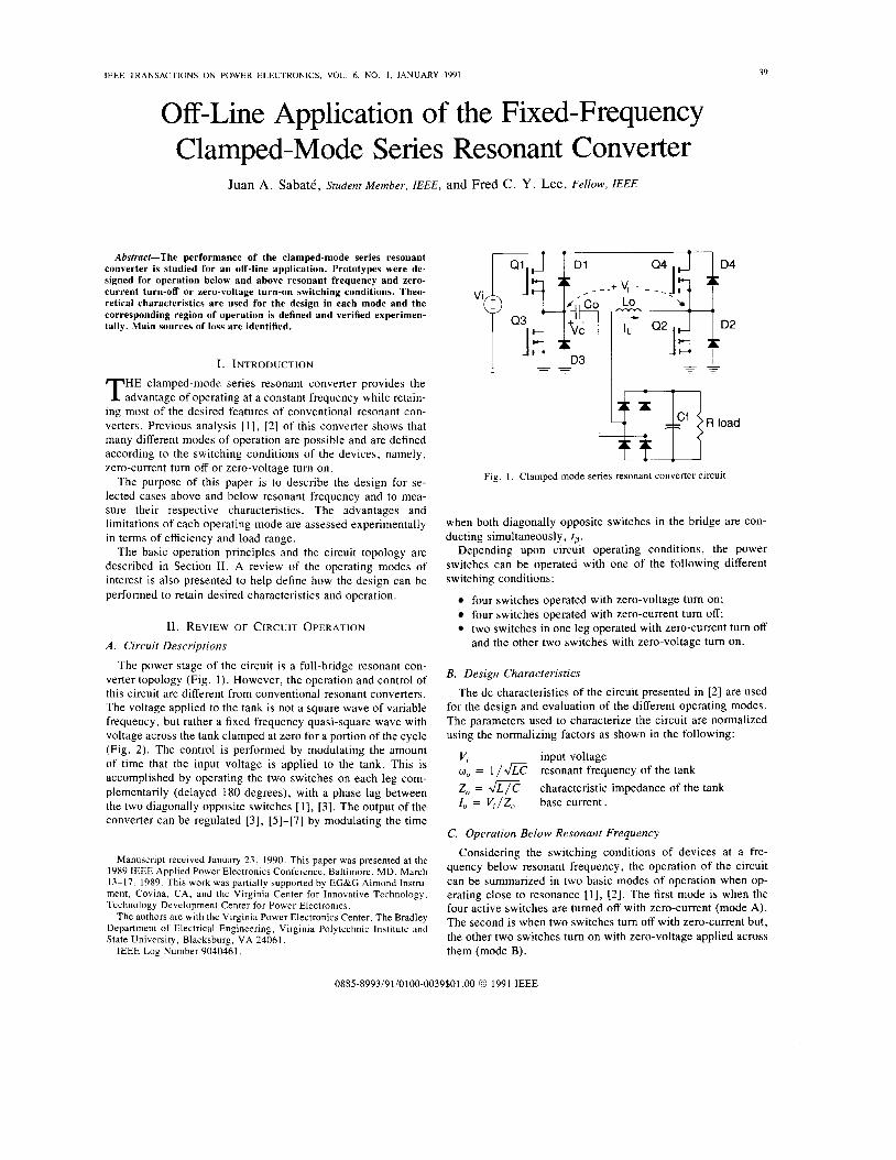
IEEE TRANSACTIONS ON POWER ELECTRONICS, VOL 6. NO I , JANUARY 1991
Off-Line Application of the Fixed-Frequency Clamped-Mode Series Resonant Converter
Juan A. SabatC, Student Member, IEEE, and Fred c. Y. Lee, Fellow, IEEE
Abstract-The performance of the clamped-mode series resonant converter is studied for an off-line application. Prototypes were de- signed for operation below and above resonant frequency and zero- current turn-off or zero-voltage turn-on switching conditions. Theo- retical characteristics are used for the design in each mode and the corresponding region of operation is defined and verified experimen- tally. Main sources of loss are identified.
Lo - I . INTRODUCTION
HE clamped-mode series resonant converter provides the T advantage of operating at a constant frequency while retain- ing most of the desired features of conventional resonant con- verters. Previous analysis [ l] , [2] of this converter shows that many different modes of operation are possible and are defined according to the switching conditions of the devices, namely, zero-current turn off or zero-voltage turn on.
The purpose of this paper is to describe the design for se- lected cases above and below resonant frequency and to mea- sure their respective characteristics. The advantages and limitations of each operating mode are assessed experimentally in terms of efficiency and load range.
The basic operation principles and the circuit topology are described in Section 11. A review of the operating modes of interest is also presented to help define how the design can be performed to retain desired characteristics and operation.
11. REVIEW OF CIRCUIT OPERATION
A . Circuit Descriptions
The power stage of the circuit is a full-bridge resonant con- verter topology (Fig. 1). However, the operation and control of this circuit are different from conventional resonant converters. The voltage applied to the tank is not a square wave of variable frequency, but rather a fixed frequency quasi-square wave with voltage across the tank clamped at zero for a portion of the cycle (Fig. 2). The control is performed by modulating the amount of time that the input voltage is applied to the tank. This is accomplished by operating the two switches on each leg com- plementarily (delayed 180 degrees), with a phase lag between the two diagonally opposite switches [ 1 3 , [3]. The output of the converter can be regulated [3], [5]-[7] by modulating the time
Manuscript received January 23, 1990. This paper was presented at the 1989 IEEE Applied Power Electronics Conference, Baltimore, MD, March 13-17, 1989. This work was partially supported by EG&G Almond Instm- ment, Covina, CA, and the Virginia Center for Innovative Technology, Technology Development Center for Power Electronics.
The authors are with the Virginia Power Electronics Center, The Bradley Department of Electrical Engineering, Virginia Polytechnic Institute and State University, Blacksburg, VA 24061.
IEEE Log Number 9040461.
T- Q2d 4”’
39
Fig. 1. Clamped mode series resonant converter circuit.
when both diagonally opposite switches in the bridge are con- ducting simultaneously, to.
Depending upon circuit operating conditions, the power switches can be operated with one of the following different switching conditions:
four switches operated with zero-voltage turn on; four switches operated with zero-current turn off two switches in one leg operated with zero-current turn off and the other two switches with zero-voltage turn on.
B. Design Characteristics The dc characteristics of the circuit presented in [ 2 ] are used
for the design and evaluation of the different operating modes. The parameters used to characterize the circuit are normalized using the normalizing factors as shown in the following:
Vi input voltage w, = 1 / f i Z , = I,, = V , / Z , base current.
resonant frequency of the tank characteristic impedance of the tank
C. Operation Below Resonant Frequency Considering the switching conditions of devices at a fre-
quency below resonant frequency, the operation of the circuit can be summarized in two basic modes of operation when op- erating close to resonance [I] , [2]. The first mode is when the four active switches are turned off with zero-current (mode A). The second is when two switches turn off with zero-current but, the other two switches turn on with zero-voltage applied across them (mode B).
0885-899319110100-0039$01 .OO 0 1991 IEEE
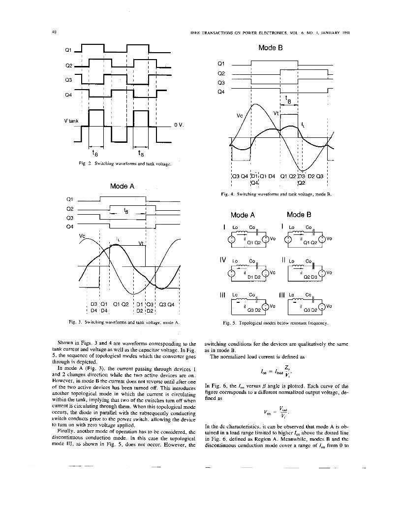
40 IEEE TRANSACTIONS ON POWER ELECTRONICS, VOL. 6, NO. I . JANUARY 1991
I 1. I I
I I
' I 1 1 ' I I ,
Fig. 2. Switching waveforms and tank voltage.
Mode A
Q1 I I
0 2 L - tL% 4 ,
Q3 - 1 I I
Q4 I I
I I 1 I 1 1 I I 1 I I 1 I I 1 I
I D31Q1 I Q1 Q2 I D1 IQ31 Q3Q4 I ! D 4 ; D 4 ; ! D21D2; I
Fig. 3. Switching waveforms and tank voltage, mode A
Shown in Figs. 3 and 4 are waveforms corresponding to the tank current and voltage as well as the capacitor voltage. In Fig. 5 , the sequence of topological modes which the converter goes through is depicted.
In mode A (Fig. 3), the current passing through devices 1 and 2 changes direction while the two active devices are on. However, in mode B the current does not reverse until after one of the two active devices has been turned off. This introduces another topological mode in which the current is circulating within the tank, implying that two of the switches turn off when current is circulating through them. When this topological mode occurs, the diode in parallel with the subsequently conducting switch conducts prior to the power switch, allowing the device to turn on with zero voltage applied.
Finally, another mode of operation has to be considered, the discontinuous conduction mode. In this case the topological mode 111, as shown in Fig. 5, does not occur. However, the
Mode B
Q1 J 1
Q2 I I I
Q3 I I I I I I
I
I I
Q4 I -!, I r
Fig. 4. Switching waveforms and tank voltage, mode B.
Mode A Mode B
IV Lo CO II Lo CO
D1 D2 Q2 D3 I I I I
Q3 D2 0 3 D2
Fig. 5 . Topological modes below resonant frequency.
switching conditions for the devices are qualitatively the same as in mode B.
The normalized load current is defined as
In Fig. 6, the I,, versus f i angle is plotted. Each curve of the figure corresponds to a different normalized output voltage, de- fined as
VO", v,, = - v , ' In the dc characteristics, it can be observed that mode A is ob- tained in a load range limited to higher I,, above the dotted line in Fig. 6, defined as Region A. Meanwhile, modes B and the discontinuous conduction mode cover a range of Io, from 0 to
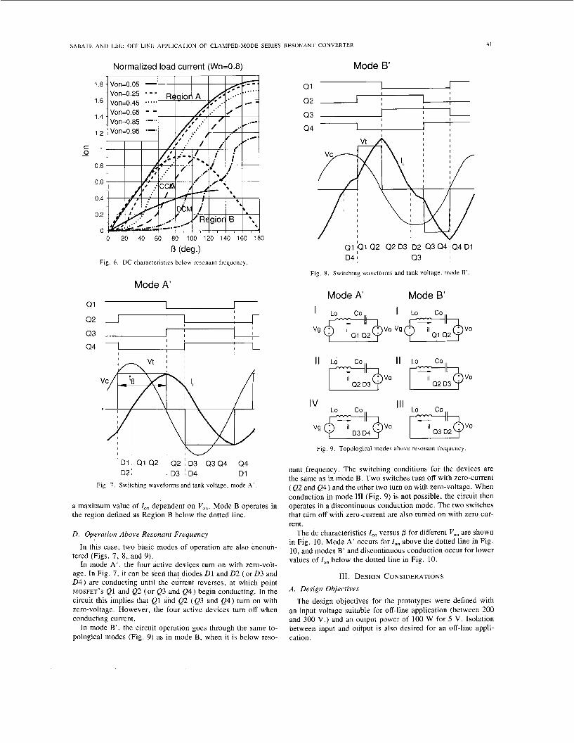
SABATE AND LEE: OFF-LINE APPLICATION OF CLAMPED-MODE SERIES RESONANT CONVERTER
~
41
Normalized load current (Wn=0.8) 1
1.8 - Von=0.05 Von=0.25
l.6 Vork0.45
1,4 Von=0.65 . Von=0.85
,2 . Von=0.95
-
0 20 40 60 80 100 120 140 160 180
0 (deg.) Fig. 6 . DC characteristics below resonant frequency.
Mode A'
Q1 I
I I /
l D 1 : Q1Q2 1 Q2 ID31 Q3Q4 I Q 4 ~
1 D2i 1 D3 I D41 ! D l
Fig. 7. Switching waveforms and tank voltage, mode A'.
a maximum value of I,, dependent on Van. Mode B operates in the region defined as Region B below the dotted line.
D. Operation Above Resonant Frequency
In this case, two basic modes of operation are also encoun- tered (Figs. 7, 8, and 9).
In mode A', the four active devices turn on with zero-volt- age. In Fig. 7, it can be seed that diodes D1 and 0 2 (or 0 3 and 0 4 ) are conducting until the current reverses, at which point MOSFET'S Ql and Q2 (or Q3 and Q 4 ) begin conducting. In the circuit this implies that Ql and Q2 ( Q 3 and Q 4 ) turn on with zero-voltage. However, the four active devices turn off when conducting current.
In mode B', the circuit operation goes through the same to- pological modes (Fig. 9) as in mode B, when it is below reso-
Mode B'
Q1 I I
Q2 1 Q3
I I
I
Q4 I t I
I I I I 1
I 1
;Q1 ;Q1 Q2 j Q2 D3 ID2 jQ3 Q4 jQ4 D1 ID41 193 I
Fig. 8. Switching waveforms and tank voltage, mode B ' .
Mode A' Mode B'
Lo Co.. IV I ' I Lo CO,,
Fig. 9. Topological modes above resonant frequency
nant frequency. The switching conditions for the devices are the same as in mode B . Two switches turn off with zero-current ( Q2 and Q 4 ) and the other two turn on with zero-voltage. When conduction in mode 111 (Fig. 9) is not possible, the circuit then operates in a discontinuous conduction mode. The two switches that turn off with zero-current are also turned on with zero cur- rent.
The dc characteristics I,, versus f i for different V,, are shown in Fig. 10. Mode A' occurs for I,, above the dotted line in Fig. 10, and modes B' and discontinuous conduction occur for lower values of Ion below the dotted line in Fig. 10.
111. DESIGN CONSIDERATIONS A. Design Objectives
The design objectives for the prototypes were defined with an input voltage suitable for off-line application (between 200 and 300 V.) and an output power of 100 W for 5 V. Isolation between input and output is also desired for an off-line appli- cation.
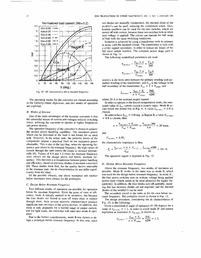
42 IEEE TRANSACTIONS ON POWER ELECTRONICS, VOL. 6, NO. 1. JANUARY 1991
2.2
2
1.8
1.6
1.4
1.2 C - 0 1
0.8
0.6
0.4
0.2
0
Normalized load current (Wn=l.2)
0 20 40 60 80 100 120 140 160 180
fi (deg.) Fig. 10. DC characteristics above resonant frequency.
The operating modes for the converter are chosen according to the formerly-stated objectives, and two modes of operation are explored.
B. Modes of Interest One of the main advantages of the resonant converter is that
the sinusoidal nature of current and voltages reduces switching losses, allowing the converter to operate at higher frequencies and power density.
The operation frequency of the converter is chosen to achieve the desired power handling capability. The maximum power which can be delivered to the load is not bound for an ideal tank. However, in the actual tank, the parasitic losses of the components impose a practical limit on the maximum power obtainable. This is due to the fact that, when the operating fre- quency gets closer to the resonant frequency, the high values of current through the tank causes the losses to increase dramati- cally [4]. Values of 0.8 and 1.2 times the resonant frequency were chosen for the design above and below resonant fre- quency. This decision is a compromise between power handling and efficiency, based on previous studies of resonant converters 141. These studies show that, for the quality factors attainable in the resonant tank, the dc characteristics do not differ signif- icantly from the ideal.
Of the possible choices, one above resonance and another below resonance were chosen for the prototypes.
C. Design Below Resonant Frequency
Two different modes of operation are possible for operation below the resonant frequency. From the point of view of effi- ciency, mode A initially seemed to be attractive, but because the four diodes are forced to turn off when there is current through them, their reverse recovery characteristics produce significant turn-on losses in the active devices. In addition, this mode is only attainable for a limited range of output current, and for light loads, the converter will enter into mode B oper- ation.
Due to the former considerations, mode B was chosen to de- sign a prototype below resonant frequency. In this case, since
two diodes are naturally commutated, the internal diode of the MOSFET’S can be used, reducing the component count. Also, lossless snubbers can be used for the two switches which are turned off with current, because these two switches turn on when zero-voltage is applied. The circuit can operate for full range of load with the same switching conditions.
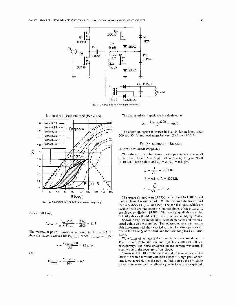
Isolation is achieved by using a transformer with its primary in series with the resonant circuit. The transformer is built with a center tapped secondary, in order to reduce the losses of the full wave output rectifier. The complete power stage used is shown in Fig. 1 1 .
The following normalized parameters are used:
where n is the turns ratio between the primary winding and sec- ondary winding of the transformer, and V,,, is the voltage in the half secondary of the transformer Vsec = 5 + Vdiode, and
where 20 A is the nominal output current. In order to operate in the forced commutation mode, the max-
imum value of I,,, cannot exceed a certain value. Mode B oc- curs below the dotted line in Fig. 6. A value Ion(max) = 0.9 is chosen.
In order to have &,,ax = 1 10 deg . in Region B , a value Van ( )
= 0.8 is chosen; then
and
the characteristic impedance is then
The operation region is depicted in Fig. 12.
D . Design Above Resonant Frequency
Above the resonant frequency, two modes of operation are possible. Mode B’ works in the same way as mode B, which was used for the design below resonant frequency. In mode A’, the four active switches turn on without voltage being applied across them (which seems to be most attractive for higher fre- quencies). In addition, the four diodes tum off naturally, mean- ing that fast recovery diodes are not required, and the internal diodes of the MOSFET’S can be used.
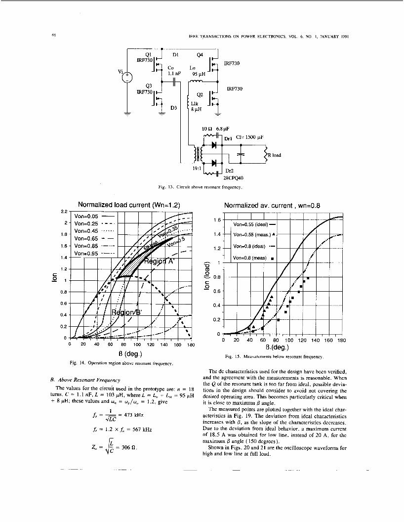
The secondary circuit is the same as for the case below res- onant frequency. The complete circuit is shown in Fig. 13.
The design procedure, considering the dc characteristics of Fig. 10, is the following:
Given a maximum p angle of operation of 150 degrees for a value of = 1 . 1 , in order to avoid mode B’ and ensure regulation at maximum 0, Ion(max) is chosen as
SABATE AND LEE: OFF-LINE APPLICATION OF CLAMPED-MODE SERIES RESONANT CONVERTER 43
c 0 -
1 .e
1.6
1.4
1.2
1
0.8
0.6
0.4
0.2
0
I-
I & I- - 1 jIli J1 , CX=+l5OOpF ~
R load -.
29: 1 USM140C
Fig. 1 1 . Circuit below resonant frequency
Normalized load current (Wn=0.8) The characteristic impedance is calculated as
Vok0.45 . . . . VOk0.65 - - VOk0.85 .-. VOn=0.95 --
0 20 40 60 80 100 .120 140 160 180
8 (deg.) Fig. 12. Operation region below resonant frequency.
then at full load,
The maximum power transfer is achieved for V,, = 0.5 [4], then this value is chosen for Vo/bn(rnax), hence = 0.35:
and
The operation region is shown in Fig. 14 for an input range 200 and 300 V and load range between 20 A and 12.5 A .
IV. EXPERIMENTAL RESULTS
A . Below Resonant Frequency
The values for the circuit used in the prototype are: n = 29 turns, C = 1.16 nF, L = 79 pH, where L = L, + L,, = 69 pH + 10 pH. These values and U , = u,/u, = 0.8 give
1 A, = - = 525 ~ H Z C C
A = 0.8 X A, = 420 kHz
Z, = 8 = 261 fl.
The MOSFET'S used were IRF730, which can block 400 V and have a channel resistance of 1 Q . The external diodes are fast recovery diodes ( r r r = 30 nsec). The serial diodes, which are used to avoid conduction of the internal diodes of the MOSFET'S, are Schottky diodes (SR.502). The rectifying diodes are also Schottky diodes (USM 140C), used to reduce rectifying losses.
Shown in Fig. 15 are the ideal dc characteristics and the mea- sured points on the prototype. The measurements are in reason- able agreement with the expected results. The discrepancies are due to the finite Q of the tank and the switching losses of MOS- FET'S.
Waveforms of voltage and current in the tank are shown in Figs. 16 and 17 for the low and high line (200 and 300 V ) , respectively. The noise observed on the current waveform is mainly due to the recovery of the diode.
Shown in Fig. 18 are the current and voltage of one of the MOSFET'S which turns off with zero-current. A high peak of cur- rent is observed during the turn on. This causes the switching losses to increase and the efficiency to be lower than expected.
44
1 0 R 6.8pF ' I C f = 1 5 0 0 p F
I
IEEE TRANSACTIONS ON POWER ELECTRONICS, VOL. 6, NO. I , JANUARY 1991
Q1 D1 -3g=, C O 1.1 nF
IRF730 4 3 pt 95 pH
-30
IRF730
" 28CPQ40
Fig. 13. Circuit above resonant frequency.
Normalized load current (Wn=l.2) Normalized av. current, w k 0 . 8 2.2
2
1.8
1.6
1.4
1.2 c 2 1
0.8
0.6
0.4
0.2
0 0 20 40 60 80 100 120 140 160 180
fi (deg-) Fig. 14. Operation region above resonant frequency.
B. Above Resonant Frequency The values for the circuit used in the prototype are: n = 18
turns, C = 1 . 1 nF, L = 103 pH, where L = Lo + L,, = 95 p H + 8 pH; these values and U, = w,/w, = 1.2, give
1 f, = - = 473 kHz
K C
1.6
1.4
1.2
- 1 U m 0
c 0
0.8
- 0.6
0.4
0.2
0 0 20 40 60 80 100 120 140 160 180
0, (d eg . ) Fig. 15. Measurements below resonant frequency.
The dc characteristics used for the design have been verified, and the agreement with the measurements is reasonable. When the Q of the resonant tank is too far from ideal, possible devia- tions in the design should consider to avoid not covering the desired operating area. This becomes particularly critical when it is close to maximum 0 angle.
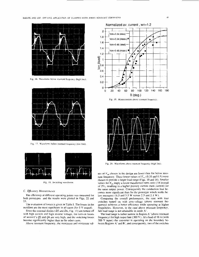
The measured points are plotted together with the ideal char- acteristics in Fig. 19. The deviation from ideal characteristics increases with 0 , as the slope of the characteristics decreases. Due to the deviation from ideal behavior, a maximum current of 18.5 A was obtained for low line, instead of 20 A, for the maximum 0 angle ( 150 degrees).
Shown in Figs. 20 and 2 1 are the oscilloscope waveforms for high and low line at full load.
SABATE AND LkE OFF LINE APPLICATION OF CLAMPED MODE SERIES RESONANT CONVERTER 45
Fig. 16. Waveforms below resonant frequency (high line)
Normalized av. current , wn=l.2 I I I I I I I I I I
1.4
1.2
Von=0.49 (ideal) --
/ I : A
A . !. 0.4
0.2 ,/
I I I I I I
0 20 40 60 80 100 120 140 160 180
fi (deg.1 Fig. 19. Measurements above resonant frequency.
Fig. 17. Waveforms below resonant frequency (low line).
Fig. 20. Waveforms above resonant frequency (high line).
Fig. 18. Switching waveforms.
C. Eflciency Measiirenierits
The efficiency at diferent operating points was measured for both prototypes and the results were plotted in Figs. 22 and 23.
The evaluation of losses is given in Table I . The losses in the rectifiers are the most significant in all cases (for 5 V output).
Since the external diodes ( 0 2 and 0 4 , Fig. 11) are turned off with high current and high reverse voltage, the turn-on losses of MOSFET'S Q2 and Q4 are very high, and the switching losses become significantly higher than in the other cases.
Above resonant frequency, the maximum and minimum val-
ues of V,, chosen in the design are lower than for below reso- nant frequency. These lower values of V,, ( 0 . 3 5 and 0 . 5 ) were chosen to provide a larger load range (Figs. 10 and 14). Smaller values for V,,, imply a lower transformer turns ratio ( 18 instead of 29), resulting in a higher primary current (tank current) for the same output power. Consequently the conduction loss be- comes more significant than for the prototype which works be- low resonance (6 .5 and 3.5 W versus 2.5 and 2.1 W ) .
Comparing the overall performance, the case with four switches turned on with zero-voltage (above resonant fre- quency) achieves a better efficiency while operating at higher frequencies. However, in the case above resonant frequency, full load range is not attainable in mode A'.
The load range is rather narrow in Region A' (above resonant frequency) for high imput line ( 3 0 0 V ). At a load of 18 A (with 300 V input) the converter is operating on the boundary be- tween Regions A' and B', and consequently, two of the switches
46 IEEE TRANSACTlONS ON POWER ELECTRONICS, VOL. 6, NO. I , JANUARY 1991
Fig. 21. Waveforms above resonant frequency (low line).
Efficiency Wn=l 2 (measured)
%
4 6 8 10 12 14 16 18 20 lout
Fig. 22. Efficiency below resonant frequency.
Efficiency Wn=l 2 (measured)
4 6 8 10 12 14 16 18 20 lout
Fig. 23. Efficiency above resonant frequency.
Norm. freq. Input voltage Output current Induct and tr. Recifier Conduction Communt. ( + rest) Snubber Efficiency
TABLE I EVALUATION OF LOSSES
0.8 0.8 1.2 1.2 200 300 200 300 21.5 21.5 18 18
4 4.0 3.0 3.5 14.3 14.3 12.0 12.0 2.5 2 .1 3.5 3.7
10.3 16.1 3.5 13.5 1.5 1.5
78 72 80 77 - -
1 .2 300
25 6.75 16.7 5.1 9.7 2.0 77
do not turn on with zero-voltage. Examining the loss break- down in Table I , it can be seen that for a load of 18 A, the switching loss is considerably higher than for a load of 25 A.
V. CONCLUSION The clamped mode series resonant converter (CMSRC) op-
erates at a fixed frequency with the devices turned on with zero voltage or turned off with zero-current. In addition to good switching conditions, the CMSRC has the advantage of fixed frequency operation, resulting in an easier design of magnetic components for resonant tank and filtering. This study has proved that it is feasible to use the CMSRC at a fixed frequency for an off-line application.
The clamped mode operation at a fixed frequency of the se- ries resonant converter presents a different mode of operation when the switching frequency is either above or below the res- onant frequency:
Below resonant frequency, either four devices are turned off with zero-current (mode A), or two are turned off with zero current and two are turned on with zero-voltage (mode B and discontinuous conduction).
Above resonant frequency, either four active devices are turned on with zero-voltage (mode A’), or two are turned on with zero-voltage and two are turned off with zero-current (modes B’ and discontinuous conduction).
The dc characteristics have been used for the design. Above resonant frequency, two regions of operation are defined:
Region A’, for large values of I,,, where the converter operates in mode A’ and Region B’, between no load and the boundary with Region A‘, where the converter operates in mode B’ or discontinuous conduction mode.
Below resonant frequency two regions of operation are de- fined:
Region A, where the converter operates in mode A, that occurs for large values of I,,, and Region B, where the converter operates in mode B, that ranges between no load and the bound- ary with Region A.
Two prototypes were designed and tested experimentally, one to operate in Region B below resonant frequency and the other to operate in Region A’ above resonant frequency.
The efficiency is mainly determined by the rectifier losses and the switching losses. In the case where the mode B of operation is implemented (below resonant frequency), the recovery of the diodes increases the turn-on losses of the devices dramatically. The operation mode with four switches turned on at zero-volt- age, mode A’ at above resonant frequency, shows better effi- ciency. Therefore, if higher frequencies of operation are desired, mode A’ is the better choice among the four modes of operation discussed in the paper.
REFERENCES
[ l ] F. S. Tsai, P. Materu, and F. C . Lee, “Constant frequency, clamped mode resonant converters,” in Proc. IEEE Power Elec- tronics Specialists Conf., 1987.
[2] F. S. Tsai and F. C. Lee, “Complete dc characterization of con- stant frequency clamped mode series resonant converter,” in Proc. Power Electronics Specialists Conf., 1988.
[3] J . Pitel, “Phase-modulated Resonant Power Conversion Tech- niques for high frequency inverters,” in Con$ Rec. IEEEIIAS An- nual Meeting, 1985.
141 R. Oruganti, “State plane analysis of resonant converters.” Ph.D. dissertation, Virginia Polytechnic Institute and State University, Blacksburg, Mar. 1987.
[51 F. S. Tsai, “Constant Frequency Resonant power processors,” M.S. Thesis, Virginia Polytechnic Institute and State University, Blacksburg, 1985.
[6] P. Materu and F. C. Lee, “Constant-Frequency Resonant Con- verter,” Annual Report, EG & G Almond Instrument, Covina, CA, 1986.
SABATE AND LEE: OFF-LINE APPLICATION OF CLAMPED-MODE SERIES RESONANT CONVERTER 41
[7] Y . Chin, “Constant frequency parallel resonant converter,” M . S . thesis Virginia Polytechnic Institute and State University, Blacks- burg, 1986.
[SI J. A . Sabatt, “Clamped-mode fixed-frequency series resonant converter, off-line application: analysis and implementation,” M.S. thesis, Virginia Polytechnic Institute and State University, Blacksburg, 1988.
State University, Blacksburg. Currently a Research Assistant, he is working towards a Ph.D. degree at Bradley Department of Electrical Engineering. His research interests include resonant power conver- sion, high-frequency power converters, converter topology. and anal- ysis and design of resonant power converters.
Juan A. Sabatk (S’86) received the degree in electrical engineering from the Polytechnic University of Catalunya, Barcelona, Spain, and his M.S. degree from Virginia Polytechnic In- stitute and State University in 1982 and 1988, respectively.
Between 1984 and 1986 he was a Researcher and Instructor in the Electronics Department at the Polytechnic University of Catalunya. In 1986 he joined the Virginia Power Electronics Center at Virginia Polytechnic Institute and
Fred C. Y. Lee (S’72-M’74-M’77-SM’87-F’90). and biography please turn to page 37 of this issue.
For a photogr .aph