Embed Size (px)
Citation preview
PERFORMANCE DEGRADATION OF A 7400 TTL NANO GATE DUE TO SINUSOIO--ETC(U)
AUG 80 J ALKALAY, 0 D WEINER F30602-78-C-0083iJ.CLA-KtFTFn RADC-TR-80-257 NL
1 7 il llEEY/llllllllllllmuEEIIEIIIIIII-IEllhEllEEEEE-

1,2- I M201.6
1.5
MICROCOPY RESOLUTION TEST CHARTNATIONAL BUREAU OF STANDARDS-I163-A

,, I " RADC-TR-80-257 f
August 1980Final Technical Report
, - PERFORMANCE DEGRADATION OF A1 7400 TTL NAND GATE DUE TO
SINUSOIDAL INTERFERENCE
Syracuse University 1I!1.E
Jacob AlkalayDonald D. Weiner
APPROVED FOR PUBLIC RELEASE; DISTRIBUTION UNUMITED I
This effort was funded by the Laboratory Director's Fund
ROME AIR DEVELOPMENT CENTER*Air Force Systems Command!C: Griffiss Air Force Base, New York 13441
80 1 10 042
4IS

This report has been reviewed by the RADC Public Affairs Office (PA) andis releasable to the National Technical Information Service (TIS). At NTISit will be releasable to the. general public, including foreign nations.
RADC-TR-80-257 has been reviewed and is approved for publication.
APPROVED:4, -
JOHN F. SPINA.Project Engineer
APPROVED: .
DAVID C. LUKE,. Lt Colonel, USAFChief, Reliability and Compatibility Division
FOR THE COMHANqDER:
Acting Chief, Plans Office
SUBJECT TO EXPORT CONTrOL LAWS
This document contains information for manufacturing or using munitions of war.Export of the information contained herein, or release to foreign nationals-within the United States, without first obtaining an export license, is aviolation of the International Traffic in Arms Regulations. Such violationis subject to a penalty of up to 2 years imprisonment and a fine of $100,000under 22 U.S.C 2778.
Include this notice with any reproduced portion of this document.
.If your address has changed or if you wish to be resoved from the ,RADCsailing list, or if the addressee is no longer employed by your organisation,please notify RADC (RBCT) Griffiss APB NY 13441. This will assist .us inmaintaining a current mailing list.
Do .not return this copy. Retain or destroy.
- ~ ,.~CAC
0 *K

UNCLASSIFTEDSECURITY C .ASSIFICATIONOF THI S PAGE (Wh.. De.1. F,.Ir-d)
VEPORT DOCUMENTATION PAGE BFRE COSMRLETINORMC .REPN 12. GOV/T ACCESSION NO.3nE NTS CATALOG NUMBER
RADC R-8X-257 4
(- XERFORMANCE~PECRADATION 01 74d4lll. p ina echnica ptI SATE.DUE TO I1NUSOIDAL INTEFERENCE Ju 7 -Ju
1ATOo S. CONTRACT OR GRANT NUJMBER(.)
_C Jacob Alkalay
Dold Veiner\ F 42-78-C-0O83 .-
4-ePWNG ORGANIZATION NAME AND ADDRESS - 40-WtRAM ELEMENT. PROJECT, TASKSyrause nivesityAREA & WORK UNIT NUMBERS
Syracuse NY 13201 111
11. CONTROLLING OFFICE NAME AND ADDRESS t3kaAZ-,-
14. MONITORING AGENCY NAME 6 ADORESS(if different from, Controll ing Office) I5. SECURITY CLASS. (of this report)
Same UNCLASSIFIEDIS.. DECLASSIFICATION'DOWNGRADING
Approved for public release; distribution unlimited.
17, DISTRIBUTION STATEMENT (of the abstract entered ini flock 20. If different from Report)
Same
IS. SUPPLEMENTARY NOTES
RADC Project Engineer: John F. Spina (RBCT)
This effort was funded by the Laboratory Director's Fund.
19. KEY WORDS (Continue on reverse side if necoueery And identify by block number)
Electromagnetic Compatibility Cofmputer Programs
curvesl C orcdgtlicit s. Ths Seotwesriesnefr eoe
to the electromagnetic susceptibility of a single integrated circuit7400 TTL NAND gate. The investigation was carried out by means of acomputer simulation using the computer program SPICE (Simulation
DD I 'R, 1473 EDITION OF I NOV 65 IS OBSOLETE UNCLASSIFIEDSECURITY CLASSIFICATION OF THIS PAGE (*%Tn*D~~VE

UNCLASSIFIEDS CUMITY CLASSIFICATION OF THIS PA6E(mmmi Data Entered)
rogram with Integrated Circuit Emphasis). The report concentrates onthe special case of sinusoidal interference inject at various circuit
nodes. Under appropriate conditions the gate voltages and currentswere observed to suffer severe waveform distortion. The computersimulation revealed that the sinusoidal interference could cause thepropagation delays and the rise and fall times of the output waveformsto increase significantly.
GltA&I
J.e er ca t on- - --. .
Di Spci31
UNCLASSIFIEDStCumITy CLASSIFICATION 00 -- 1- PACIE'h.. Dal EMn.d

CONTENTS
Page
SECTION 1: INTRODUCTION .......... 1
SECTION 2: CIRCUIT SCHEMATIC AND OPERATIONOF 7400 TTL NAND GATE .............. 4
SECTION 3: MODELING OF 7400 NAND GATE USINGTHE SPICE COMPUTER PROGRAM. . . . .. . . . . 10
SECTION 4: LOADING OF 7400 NAND GATE AND LOCATIONOF INTERFERENCE SOURCES ............. 19
SECTION 5: REPRESENTATIVE OUTPUT WAVEFORMS WITHSINUSOIDAL INTERFERENCE INJECTED INSERIES WITH THE OUTPUT OF GATE . .3.......33
SECTION 6: DEFINITIONS OF WAVEFORM PARAMETERS FORDESCRIBING INTERFERENCE EFFECTS ......... 40
SECTION 7: RESULTS OF COMPUTER SIMULATION . ......... . . 47
SECTION 8: SUMMARY AND SUGGESTIONS FOR FUTURE WORK . . . . . 60
REFERENCES: . . . . . . . . . . . . . . . . . . . . . .. 62
APPENDIX A: CALCOMP PLOTS OF REPRESENTATIVEOUTPUT WAVEFORMS . . . . . . . . . . . . . . . .. 63
APPENDIX B: SAMPLE SPICE COMPUTER PROGRAM. . . . . . . . . . . 69
1. INTRODUCTION
A typical Air Force system includes a wide variety of electronic
equipments. Each equipment is likely to have several ports by which
electromagnetic energy is either transmitted and/or received. Ports
that generate electromagnetic energy are referred to as emitter ports
while those that receive electromagnetic energy are referred to as
receptor ports. Electromagnetic interference (EMI) is said to occur
at a receptor port when undesired signals degrade receptor performance
to an unacceptable level. The RADC Intrasystem Analysis Program (lAP)
is concerned with the problem of insuring electromagnetic compatibility
(EKC) between the various equipments within a system.
One of the most difficult problems associated with the lAP is
specification of criteria under which undesired signals do, in fact,
constitute interference to a receptor. Needed are EKI performance
curves for each receptor which relate degradation in receptor performance
to significant parameters of the undesired signals. Such performance
curves are available for most communications, radar, and navigation
receivers. However, relatively little work has been done on EKI per-
formance curves for other types of recepters.
Of particular concern is the electromagnetic susceptibility of
electronic equipments utilizing digital circuits. Recent breakthroughs
in integrated circuit and microprocessor technologies have produced a
rapid expansion in the use of digital circuits. Nevertheless, rela-
tively little attention has been devoted to their electromagnetic
~1
II I II I, .--I. .. . .,i.- ...
2
susceptibility. Specifically, EMI performance curves for digital cir-
cuits are unavailable. In fact, even though sophisticated digital
equipments employing thousands of digital circuits are colmonplace,
the effect of undesired signals on even a simple logic gate is not
clearly understood. Therefore, in the work reported herein, it was
decided to investigate the electromagnetic susceptibility of a single
integrated circuit 7400 TTL NAND gate.
The investigation was carried out by means of a computer simula-
tion using the computer program SPICE (Simulation Program with Integrated
Circuit Emphasis). Because of the small physical dimensions associated
with the integrated circuit chip, it was assumed that the most probable
mechanism for interfering signals to enter the NAND gate was due to
electric and/or magnetic fields coupling onto the long wires attached
to the chip. Consequently, interference sources were impressed on the
gateIs input, output, power line, and ground connections.
This report concentrates on the special case of sinusoidal inter-
ference in series with the gate output. Under appropriate conditions
the gate voltages and currents were observed to suffer severe waveform
distortion. This is in contrast to a previous experimental study [11,
performed by McDonnell Douglas Astronautics Company, which monitored
only dc voltage offsets. Our computer simulation revealed that the
sinusoidal interference could cause the propagation delays and the
rise and fall times of the output waveforms to increase significantly
(as much as ten times in some cases). Also, instead of experiencing
a simple dc offset, the output waveform can fluctuate between the
_ _ _ _ _.. .._I I_ _.. .L .... . . ...
# ,.I

3IHIGH and LOW states. Large variations in the power supply current were
also noted.
In order to describe the waveform distortions, it is convenient
to distinguish between transient and steady-state effects. The tran-
sient effects apply to the leading and falling edges where the wave-
form attempts to switch from one state to another. On the other hand,
the steady-state effects pertain to the periodic portion where the
waveform tries to maintain a constant output. Various waveform
parameters are defined in order to describe these effects. These
parameters are then plotted as a function of the amplitude and fre-
quency of the sinusoidal interferer.
.ko

2. CIRCUIT SCHEMATIC AND OPERATION OF 7400 TTL NAND GATE
The schematic diagram of the 7400 TTL NAND gate, as specified by
the manufacturer, is shown in Fig. la. Observe that the circuit contains
5 transistors and 3 diodes. In actuality, the two input transistors JT11 and T1 2 comprise a single dual emitter transistor with a common
collector. The diagram includes the node numbers used in the SPICE
simulation. Note that node 8 is the gate output.
The NAND gate for the two-input case is symbolized as shown in
Fig. lb. The truth table, given in Table 1, demonstrates that the
output is LOW (0) if and only if both inputs are HIGH (1).
Table 1
Truth Table for NAND Gate
VIN 1 VIN 2 V0
0 0 1
0 1 1
1 0 1
1 1 0
According to the manufacturer, an input voltage must exceed 2 volts
if it is to be interpreted as HIGH and must be below 0.8 volts if it
is to be interpreted as LOW. Similarly, the output must exceed 2.4
volts if it is to be considered HIGH and must be below 0.4 volts if
it is to be considered LOW. Typical values for the output voltages are
3.4 volts in the HIGH state and 0.2 volts in the LOW state. These levels
are summarized in Table 2.

V (+ 5V)
5
VINI % T
VIN2 @
(a)
(b)
Fig. 1. a) Schematic diagram of 7400 TTh NAND gate.b) Schematic symbol.
6
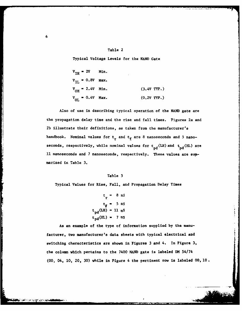
Table 2
Typical Voltage Levels for the NAND Gate
VIH - 2V Min.
VIL - 0.8V Max.
VOH W 2.4V Min. (3.4V TYP.)
V = 0.4V Max. (0.2V TYP.)
Also of use in describing typical operation of the NAND gate are
the propagation delay time and the rise and fall times. Figures 2a and
2b illustrate their definitions, as taken from the manufacturer's
handbook. Nominal values for tr and tf are 8 nanoseconds and 5 nano-
seconds, respectively, while nominal values for tpd(LH) and tpd(HL) are
11 nanoseconds and 7 nanoseconds, respectively. These values are sup-
marized in Table 3.
Table 3
Typical Values for Rise, Fall, and Propagation Delay Times
t = 8 nSr
t . 5 nS
tpd(LH) - 11 nS
tpd(HL) - 7 nS
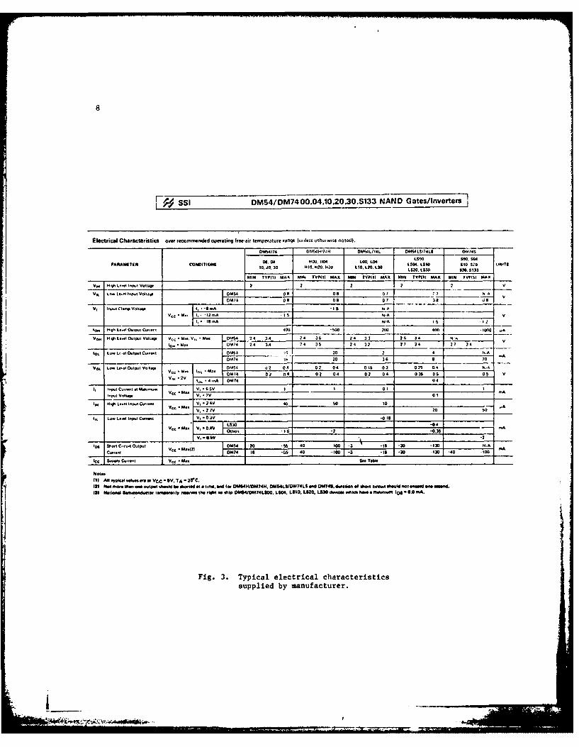
As an example of the type of information supplied by the manu-
facturer, two manufacturer's data sheets with typical electrical and
switching characteristics are shown in Figures 3 and 4. In Figure 3,
the column which pertains to the 7400 NAND gate is labeled DM 54/74
(00, 04, 10, 20, 30) while in Figure 4 the pertinent row is labeled 00, 10.
~~j~j-

7
V1
0. t
3.55
(a)
Vol2 V[ .... ZZZD2viIV --
(b)
Fig. 2. a) Propagation delay time.b) Rise and fall time.
8
SSI 0M54/DM7400.04.1O.20.30.S133 NAND Gates/inverter's
Electr'ical Char'acteristics over recortmended operating fr ee-air temperature range (un'less othetwise noted).
OW.154 DMiH7. MS411741. 0454LS174LS_ _ WA4S
FAMTECODTOS100.05 HD00 1#04 l1.104 100 000.sl S0 UIT
PARMEOA ON~TIOS 0. AO. 30 1110. H20. 1130 LI0. 20. 120 LSO. LS010 £10 0 NIT
MINd TVPlIJ MAX MINd TYPlI MAX MINd TVPIll MAX MIld TVPIl MAX MiUN TYPill MAX
Vw L" L*.llI eIMVO~s&t DM54 00 08 07 7 N A
DM4 08 O0 7 08 U
V, Ine.. CI... Vollq. I -8. L - -is N NA 5
.14,,. :!,-12.,A . l5 N,A V
1-1I,,.A NIA IS I
i~ lg5
L..l olmlo...t -0SOO -2010 W)0 --(0 .A
OM7 24__ 34 24 35, 24 32 2? 34 2,0 34
Vm 1om L.. On... Vo:,.W VM54 (, 02n Vi 3 0
Input VolI-...5', * 7 0C
Ioll 14, L*.p Inn C14 02 040 42 00 0 S750,V,. 2Vs.oos
1.~, L I ot Inpt CA oml V, 05' -O I6 1 0 1 1____
20. -06.4 -40h - .00 -2 .A 3 -3
I~ t~~ C.,U, totto -55 40 007 7 00 -3 -16 -30 -130 1-400
Oc: SeeM, C..1. V" Mo. at h.
ill All tYbocal OImi.0gstm, VCc - V, TA - 25rC.IS)No md~ore thasn ensi004 otheoWld be 410 a.M ao tomu e an o OM54I4UDM?41. DIGLSIDM?401. and 001748. dtiohn o the cerow.lroi nM0.0 eninne one tnsd
3 Melleo" Seonwettiowaae loommee-ry rtwnwm the tiel to ship DMW4OM74L.SOO. L$04. L$10. 1.526. L330 deos. vollict home a mtiomnoawn 1() .. 0 ta.
Fig. 3. Typical electrical characteristicssupplied by manufacturer.

9
SSSI DM54/DM7400.04,1O.20,30,S133 NAND Gates/Invertr
Switching Chareristics at Vc - 5V. TA, - 2rC
Propoption Delay Timne. Progiaption Delay rm.DEVICE CONDITIONS Law-To-High Leiwi Output Niell-To-Low Level Output
MIN TYP MAX MIN TYP MAX
00.10 11 22 7 1s04.20 C,. ISpF. tL 4OOn 12 22 8 15
30________ 13 22 8 15
t LOO 6.9 10 6.2 101404 6 10 6.5 101410 CL -2S pF. RL 280al 6.9 10 6.3 101420 6 10 7 10H430 ________ 6.8 10 8.9 12
LOO. L043S S31 6LIO. L20 CL - 0 pF.RL.~ 3- 60 31 6L30 36 60- 70 100LSOO. LSO4 9 1 0 iLSIO.LS7O CL -t5 pF. RL~2f 9 15 10LS30 9 15 16 2'1
Soo.S04l CL -ISoF. RL -280nl 2 3 4.6 2 3 6SIO.S20 Ct. 60pF. RL* 2
- Ma 4.5 7 5 a
S3.I3 CL -I15PF.ARL -280n 2 4 6 2 4.5 7____CL - 50 F. AL -280nl 6.6 8 6.5 10
Fig. 4. Typical switching characteristicssupplied by manufacturer.

10
3. MODELING OF 7400 NAND GATE USING THE SPICE COMPUTER PROGRAM
The susceptibility of the 7400 NAND gate was investigated using
the SPICE computer program in its transient mode of operation. This
required a detailed circuit modeling of the 7400 NAND gate. As shown
in Fig. la, typical resistor values are provided by the manufacturer.
However, circuit models for the transistors and diodes are not supplied.
Fortunately, the SPICE computer program does contain stored circuit
models for both the bipolar junction transistor (BJT) and the semi-
conductor diode. Typical parameter values, for use in the models,
are also found in the SPICE User's Manual [2].
Another source which was useful in the circuit modeling was the
McDonnell Douglas study [1] previously cited. To explain the dc
voltage effects which they had measured, they developed a modified
transistor model. This was exercised using the SPICE computer program
in its dc mode of operation. They modeled a 7400 NAND gate and listed
the numer*.cal values used for the dc parameters of the 5 transistors
and 3 diodes of Fig. la. Note that capacitive parameters were not
specified since their dc analysis required only resistive components.
Our approach was to begin with the parameter values specified
by McDonnell Douglas. For those parameters not specified by McDonnell
Douglas, typical values taken from the SPICE User's Manual were used.
The circuit was then exercised with the SPICE program and certain
parameter values were adjusted in an attempt to achieve circuit per-
formance as close as possible to the manufacturer's specifications.
This resulted in 3 parameters having values different from those of
_ _ _ _ _ _

11
McDonnell Douglas and 2 parameter values differing from typical SPICE
values.
The SPICE transistor model is shown in Fig. 5. It is based upon
the integral charge control model of Gummel and Poon. The 27 parameters
required by the model are listed in Table 4 along with their typical
SPICE values.*
The SPICE diode model is shown in Fig. 6. This model makes use
of 11 parameters. These are listed in Table 5 along with their
typical SPICE values.
Table 5
SPICE Diode Model Parameters
Typical
Symbol Parameter Name Units Values
is Saturation current amps L.OE-14
r Ohmic resistance ohms 10
n Emission coefficient - 1.0
Tt Transit time sec 0.1 nS
Cjo Zero-bias junction capacitance farad 2 pF
B Junction potential volts 0.6
m Grading coefficient - 0.5
£ Energy gap eV 1.11 SI9 0.69 SBD
0.67 GE
PT Saturation current temperature exponent - 3.0 JN2.0 SBD
Kf Flicker-noise coefficient - 0
af Flicker-noise exponent - 1
Table 4 appears on page 12.

12
Table 4
SPICE BJT Model Parameters
Symbol Parameter Name Units Typical Value
BF Ideal forward current-gain coefficient - 100
BR Ideal reverse current-gain coefficient - 0.1
IS Saturation current amps L.OE-16
rb Base ohmic resistance ohms 100
r Collector ohmic resistance ohms 10cr Emitter ohmic resistance ohms 1
V Forward Early voltage volts 200
VB Reverse Early voltage volts 200
IK Forward Knee current amps lOMA
C2 Forward nonideal base current coefficient - 1000
nEL Nonideal b-e emission coefficient - 2.0
IKR Reverse knee current amps 100mA
C4 Reverse nonideal base current coefficient - 1.0
nCL Nonideal b-c emission coefficient - 2.0
tF Forward transit time sec O.InS10 nSTR Reverse transit time seC
CCS Collector-substrate capacitance farads 2 pF
C Zero-bias b-e junction capacitance farads 2 pFjee B-E junction potential volts 0.7
m B-E junction grading coefficient - 0.33eC Zero-bias b-c Junction capacitance farads 1 pFjc
B-C junction potential volts 0.5
m B-C junction grading coefficient - 0.33
E Energy gap eV 1.11 SI0.67 GE
PT Saturation current temperature exponent -
Kf Flicker-noise coefficient - 6.6E-16 NPN6.3E-13 PNP
af Flicker-noise exponent 1.0 NPN1.5 PNP

13
C
vec
F e Ic
Fig. 5. The SPICE BUT Model.

14
+
Fig. 6. The SPICE semiconductor diode model.

15
The diode and transistor parameter values used by McDonnell
Douglas in their dc computer simulation of the 7400 NAND gate are pre-
sented in Table 6.
Table 6
McDonnell Douglas Diode and Transistor Parameter Values
Diode Parameters
Name Parameter Description DIN D3
RS Ohmic resistance (Q) 60 30
IS Saturation current (pA) 100 5
Transistor Parameters
Name Parameter Description Tl T2 T3 T4
BF Forward Bets (SF) .316 19.8 17.2 21.7
BR Reverse Beta (OR) .0024 .060 .082 .106
RB Base Ohmic Resistance (Q) 68. 75. 70. 80.
IS Saturation current (pA) .5 3. 8. 20.
AFa Forward alpha (aF) .24 .952 .945 .956ARa Reverse alpha (aR) .0024 .057 .076 .0956
IESa Emitter diode sat.curr (pA) 2. 3. 8. 20.
ICSa Collector diode sat. 200. 50. 100. 200.current (pA)
aparameter used in modified Ebers-Moll model.
16
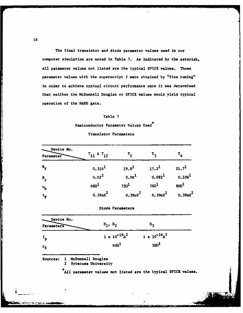
The final transistor and diode parameter values used in our
computer simulation are noted in Table 7. As indicated by the asterisk,
all parameter values not listed are the typical SPICE values. Those
parameter values with the superscript 2 were obtained by "fine tuning"
in order to achieve typical circuit performance once it was determined
that neither the McDonnell Douglas or SPICE values would yield typical
operation of the NAND gate.
Table 7
Semiconductor Parameter Values Used
Transistor Parameters
Device No. S&. T2 T3 T4
Parameter 11 12 2 3 4
Bf 0.3161 19.81 17.21 21.71
B 0.022 0.061 0.0821 0.1061r
rb 6801 751l 1 70n 1 80 1
T? 0.39nS2 0.39nS2 0.39nS2 0.39nS2
Diode Parameters
Device No.
Parmeters D1, D2 D3
IS 1 x 10- 16A2 1 x 10⁻¹ 6A2
rS 6001 3001
Sources: 1 McDonnell Douglas2 Syracuse University
All parameter values not listed are the typical SPICE values.

17
The justification and effect of using parameter values different
from those of McDonnell Douglas and SPICE are given in Table 8. All
of the parameter values finally decided upon are considered to be
reasonable.
Table 8
Justification and Effect of Parameter Changes
Parameters differing from McDonnell Douglas
ChangeParameter From To Justification Effect
Br(T1 ) 0.0024 0.02 More typical to TTL input Current levelstransistor (see Ref. 3). closer to manu-
facturer's speci-fication
IS(tran- 10-1 2A 10- 16A Typical SPICE value Rise/fall times,sistors) propagation delays
and voltage levels
closer to manu-facturer's speci-fications
Is(Diodes) 10- 12A 10-1 6A More reasonable value Voltage andcurrent levelscloser to manu-facturer's speci-fications
Parameters differing from typical SPICE valuesChange
Parameter From To Justification Effect
TF 0.lnS 0.39nS Morb appropriate for a Gives more reasonableswitching transistor base-emitter capaci-
tance
IS (Diodes) 10- 14A 10-1 6A More reasonable value Voltage and currentlevels closer to
manufacturer'sspecifications.
18
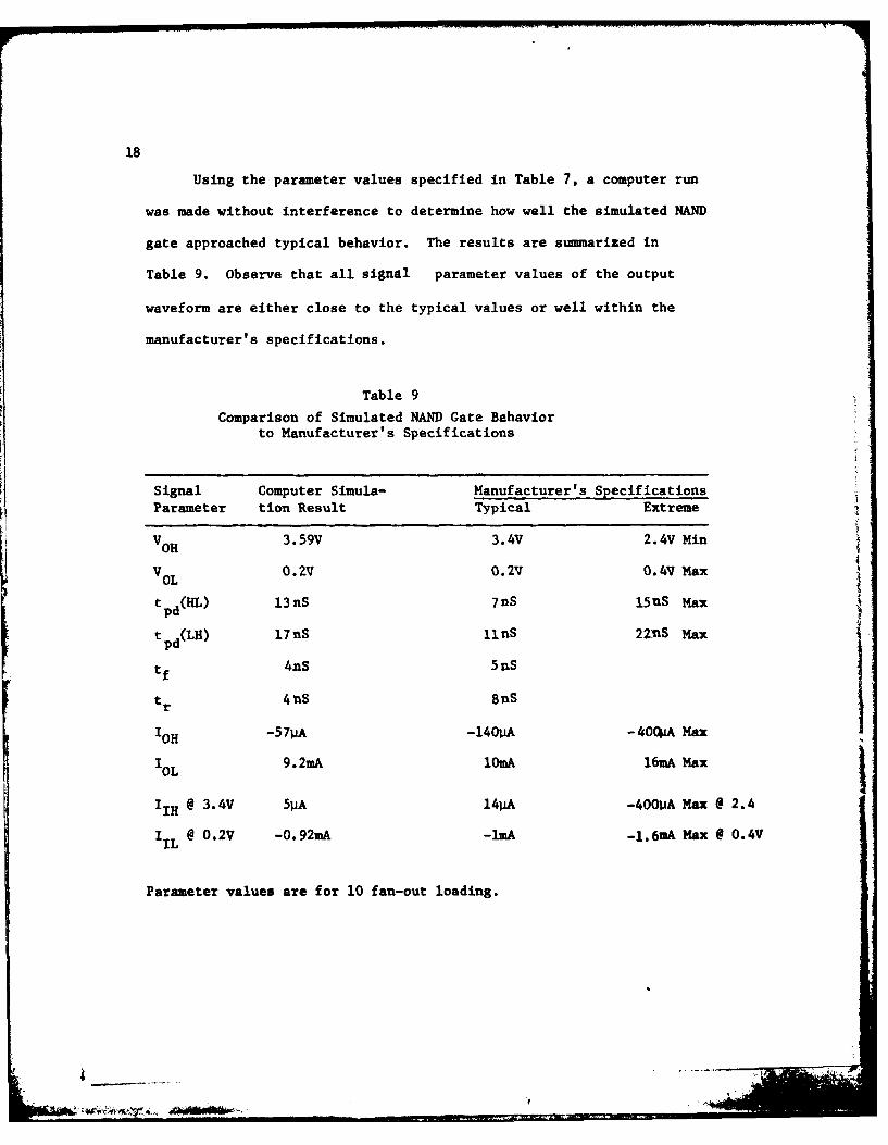
Using the parameter values specified in Table 7, a computer run
was made without interference to determine how well the simulated NAND
gate approached typical behavior. The results are summarized in
Table 9. Observe that all signal parameter values of the output
waveform are either close to the typical values or well within the
manufacturer's specifications.
Table 9
Comparison of Simulated NAND Gate Behaviorto Manufacturer's Specifications
Signal Computer Simula- Manufacturer's SpecificationsParameter tion Result Typical Extreme
HO VOH 3.59V 3.4V 2.4V Mmn
VOL 0.2V O.2V 0.4V Max
tpd(HL) l3nS 7nS 15 uS Max
t pd(LH) 17nS llnS 22nS Max
tf 4nS 5nS
tr 4nS 8nS
IOH -57iA -140vA - 4009A Max
IOL 9.2mA 10mA 16mA Max
IIH @ 3.4V 5 A 141A -400uA Max @ 2.4
IIL @ 0.2V -0.92mA -lmA -1.6mA Max @ 0.4V
Parameter values are for 10 fan-out loading.

19
4. LOADING OF 7400 NAND GATE AND LOCATIONOF INTERFERENCE SOURCES
In contrast to McDonnell Douglas who loaded their gate with a
fixed resistor in order to approximate a fan-out of 10 gates, we
loaded our gate with a second 7400 NAND gate which was impedance
scaled so as to also simulate a fan-out of 10 gates. The impedance
scaling was accomplished by using the model of the first gate with
all resistance values divided by 10, all capacitance values multi-
plied by 10 and all saturation currents multiplied by 10. This
resulted in the currents of the second gate being increased by a factor
of 10 while the time constants (i.e., RC products) and voltages
(i.e.,RI products) of the second gate remained unchanged from those
of the first gate.
By loading the first gate with a second gate, we have more ac-
curately modeled a typical circuit configuration. The time-variant and
nonlinear nature of the load is taken into account as the second gate
is caused to switch states. In addition, interference applied at
the output of the first gate is also injected into the second gate.
This more accurately depicts what is apt to happen in practice. Finally,
by observing the output of the second gate, it is possible to deter-
mine whether waveform distortion in the output of the first gate is
severe enough to cause undesired state changes in the output of the
second gate. A fan-out of 10 gates was used because manufacturer's
specifications are often given in terms of this type of loading. Also, I'__I

20
it was anticipated (and subsequently confirmed) that the first gate
is more susceptible to EDI when loaded with a fan-out of 10 as opposed
to a fan-out of 1.
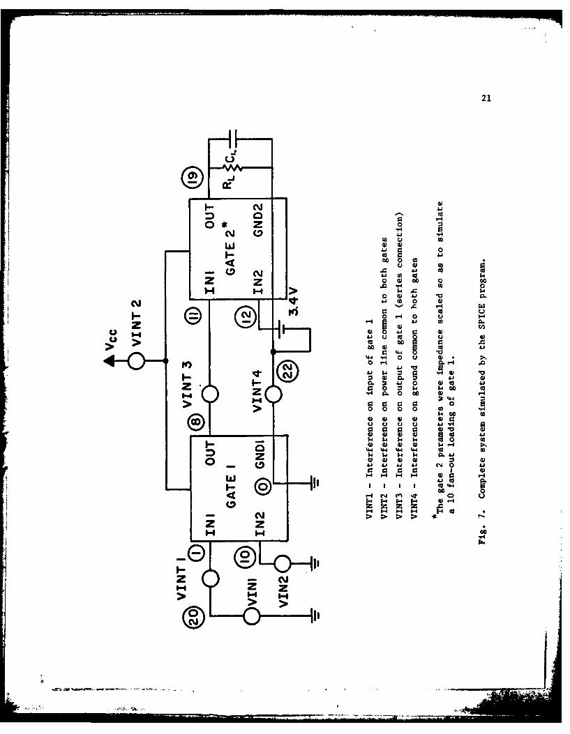
The entire system simulated by the SPICE program is shown in
Fig. 7. For convenience, the second gate was loaded by the parallel
combination of a fixed resistor and capacitor to ground. In order
to simulate a fan-out of 10 gates, RL and CL were set equal to 400
ohms and 15 pF, respectively. In addition, VIN2 of the second gate
(node 12) was maintained at the HIGH voltage level of 3.4 volts. The
truth table for the two gates of Fig. 7 is given in Table 10. V(l)
and V(1O) denote the two inputs of the first gate. V(8) denotes the
output of the first gate while V(19) denotes the output of the second
gate. With VIN2 of the second gate (node 12) held HIGH, note that
the output of the second gate changes state whenever the output of
the first gate changes state.
Table 10
Truth Table for Two Gates of Fig, 7
V(l) V(I0) V(8) V(19)
0 0 1 0
0 1 1 01 0 1 01 1 0 1
The network topology of gate 2 is identical to that of gate 1
as given in Fig. la. However, the component values of gate 2 differ
from those of gate 1 because of the impedance scaling mentioned
21
C-)d
0 0 w
OS z 0 wt
0 w00
4.0 0
> c 00 4.1 A
4 .4 .3 C
41 0 1
Zz 0 CC4 0 4)ca 4N0 144 w 0 t
D: 4.4 :30
>0 0 0 4
I- (Q 9~0 '-0 0 4 -4
0 CC 0 044 4 4 04 to
'4- w 4 0 0 *3
4.w. @ 0 1 *w4
00 00
1444 4 10 C0 H3 E -4 c:>. :>- >44 I. ~ 0C
14 14 14 14 0.-
22
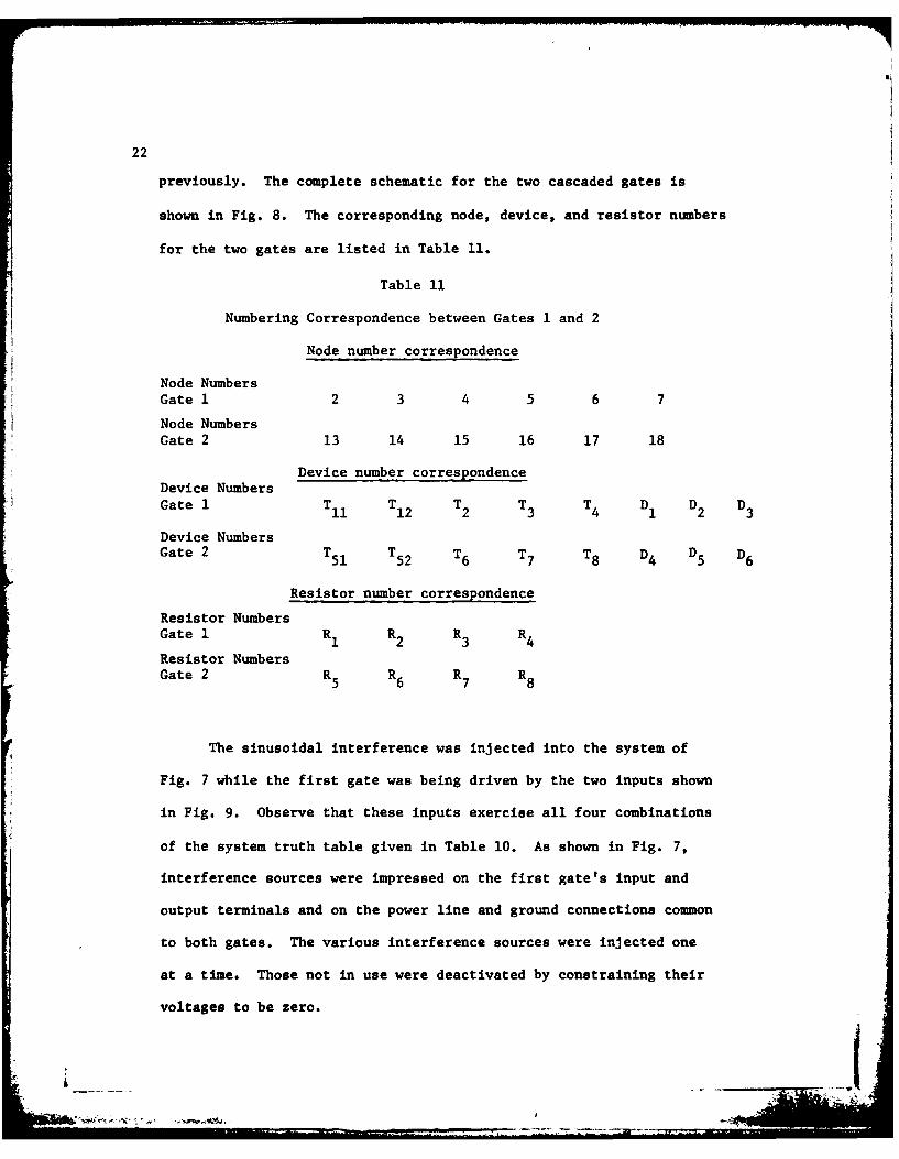
previously. The complete schematic for the two cascaded gates is
shown in Fig. 8. The corresponding node, device, and resistor numbers
for the two gates are listed in Table 11.
Table 11
Numbering Correspondence between Gates 1 and 2
Node number correspondence
Node NumbersGate 1 2 3 4 5 6 7
Node NumbersGate 2 13 14 15 16 17 18
Device number correspondenceDevice NumbersGate I TI1 T12 T2 T3 T4 D1 D2 D3
Device NumbersGate 2 T51 T52 T6 T7 T8 D4 D5 D6
Resistor number correspondence
Resistor NumbersGate 1 R1 R2 R3 R4
Resistor NumbersGate 2 R5 R6 R7 R8
The sinusoidal interference was injected into the system of
Fig. 7 while the first gate was being driven by the two inputs shown
in Fig. 9. Observe that these inputs exercise all four combinations
of the system truth table given in Table 10. As shown in Fig. 7,
interference sources were impressed on the first gate's input and
output terminals and on the power line and ground connections common
to both gates. The various interference sources were injected one
at a time. Those not in use were deactivated by constraining their
voltages to be zero.
23
ciiC: t-
cc
00
'4
0
u
+ U441
UAuI
0
cl:
to0
c'.

24
3.4 V
v(Io)
0.2V
3.4 V
-(1
0.2 V
I st 2nd 3 rd 4thQUARTER QUARTER QUARTER QUARTER
The input rise/fall times were set equal to 5nS forcomputer simulation.
The pulse widths were allowed to vary depending uponthe interference frequency.
Fig. 9. Input waveforms used to drive the first gate
while sinusoidal interference was injectedinto the system of Fig. 7.

25
Depending upon the point at which the interference was injected,
it was discovered that the system was most susceptible to sinusoidal
interference during certain quarters of the input, as defined in Fig. 9.
For example, the fourth quarter was found to be most critical when the
interference was applied either in series with the output of gate I
(VINT 3) or in the ground line (VINT 4). As shown in Fig. 10, a I MHz
sinusoidal interferer of amplitude 3V did not cause any noticeable
interference on the output of gate 2 during the first three quarters
but did result in fluctuations between the HIGH and LOW states during
the fourth quarter. Similarly, when the same interference was applied
to the input of gate 1 (VINT 1), the system was observed to be sus-
ceptible during the second and fourth quarters, as shown in Fig. 11.
Finally, with a I MHz interferer of amplitude 5V injected into the
power line (VINT 2), the system was found to be susceptible during the
first three quarters but not in the fourth. This is illustrated in
Fig. 12. Although severe fluctuations did occur on the output of
gate 2 during the fourth quarter, the system is not considered to be
susceptible during this quarter since the output did not fall below
2V (i.e., did not change states).
It was also discovered that the system is most susceptible to
sinusoidal interference applied in series with the output of gate 1
(VINT 3) as opposed to interference injected into the input of gate 1
(VINT 1), the power line (VINT 2), and the ground line (VINT 4). This
is illustrated in Fig. 13 where the minimum interference amplitude
required to cause the steady-state portion of the gate 2 output to

26
GATE 2 OUTPUTa (PERTURBED)
-~-GATE 2 OUTPUT
3 /L-s -61Ls 9/iS12 s
QURE S j 2nd 3rd 4th
I QARTRIQUARTER dURE QURE
Fig. 10. output of gate 2 with a 1 MH9 sinusoidalinterferer of amplitude 3V applied either
in series with the output of gate 1 (VINT 3)I
or in the ground line (VINT 4).

27
GATE 2 OUTPUT(NORMAL)
3.4 V /
GATE 2 OUTPUT(PERTURBED)
0.2V ,
1st j 2nd 3rd 4thQUARTER QUARTER QUARTER QUARTER
Fig. 11. Output of gate 2 with a 1 MHz sinusoidal
interferer of amplitude 3V applied to theinput of gate 1 (VINT 1).

28
7V.,GATE 2 OUTPUT
(PERTURBED)
3.4 r -GATE 2 OUTPUTI I (NORMAL)
,AA0.2V - J I
03/,.s 6ps s 12jFsI st 2nd j 3rd I 4th |
QUARTER QUARTER I QUARTER I QUARTER
Fig. 12. Output of gate 2 with a 1 MHz sinusoidalinterferer of amplitude 5V injected intothe power line (VINT 2).
& __ ____ ___ _ __ ___ ____ ___

, 29
00
00
00
0 ~It
W o
z4 1
41
%to
a0 044
4+ 0
w 0~( 41+ 0 *r toI 4 .
+ [>
44
0nq r~ OD r- D In- V in c- 0
(SJ.IOA) 3a fldWV 33N33AH3.LNI
MOM" - 4-
30
change state is plotted as a function of the interference frequency.
Consistent with the previous discussion of susceptible input quarters,
the four curves in Fig. 13 pertain to the following susceptible quarters:
(1) output of gate 1 - fourth quarter, (2) input of gate 1 - second
quarter, (3) power line - first quarter, and (4) ground line - fourth
quarter. The curve for sinusoidal interference inserted in series with
the output of gate 1 displays not only the largest susceptibility but
also the broadest bandwidth. It is pertinent to point out that McDonnell
Douglas also found the NAND gate to be most susceptible to RF inter-
ference entering the gate output [1].
Consequently, in the remainder of this report, results are pre-
sented only for the case of sinusoidal interference applied in series
with the output of gate 1 (VINT 3). Recall that the system is most
susceptible to this interference during the fourth quarter of the input.
In order to examine the effect of interference during the switching
mode while reducing the running time of the simulation, only the end
of the third quarter to the steady-state portion of the fourth quarter
was simulated on the computer. Typical behavior of the two gates
during this interval without interference is illustrated in Fig. 14.
,- As a final check that the NAND gates, in the absence of inter-
ference, were functioning properly during the computer simulation,
the voltage levels at all the nodes of Fig. 8 were examined during the
third quarter (i.e. V(8) HIGH, V(19) LOW) and the fourth quarter
(i.e. V(8) LOW, V(19) HIGH). These voltages are tabulated in Table 12.
31
3.4 V
3.4 V
3.4 V
V (8)
0.2 V
3.4 V
V(019)
0.2 v
Fig. 14. Typical behavior of the two gates during the transitionfrom the third to fourth quarters without interference.
L Al

32
All of these voltages conform to typical values. In addition, the
current levels, timing sequences, and time delays all agreed with
those of a properly functioning circuit.
Table 12
Node Voltages for Third and Fourth Quarters
Third Quarter Fourth QuarterNode Number Voltages (Volts) Voltages (Volts)
20 0.2 3.4
10 0.2 3.4
2 0.9494 2.545
3 0.3022 1.882
4 4.993 1.188
5 0.0011 1.032
6 4.993 5.0
7 4.292 0.7338
8 , 11 3.589 0.2118
13 2.501 0.9993
14 1.838 0.3594
15 1.143 4.935
16 0.9878 0.0001
17 5.000 4.907
18 0.6151 4.163
19 0.0629 3.368

33
5. REPRESENTATIVE OUTPUT WAVEFORMS WITH SINUSOIDALINTERFERENCE INJECTED IN SERIES WITH THE OUTPUTOF GATE I
With the inputs of gate 1 chosen so as to transition from the
third to fourth quarters (see Fig.14), a sinusoidal interferer, VINT3,
was inserted in series with the output of gate 1 as shown in Fig. 7.
(The other interference sources in Fig. 7 were deactivated by setting
their voltages equal to zero.) The amplitude and frequency of the
interferer were varied from 0.5 to 20 Volts and from 0.1 to 200 MHz,
respectively.
For certain amplitude and frequency combinations of the inter-
ferer, severe distortion was observed in the output waveforms of
gates 1 and 2. The purpose of the simulation was to investigate the
susceptibility of the first gate. (The second gate acts merely as a
load for the first gate.) However, looking at only the distorted out-
put of the first gate, it is not clear to what extent upset will be
caused in a following gate. For this reason, attention is focused
on the output of gate 2. Recall from Fig. 14 that the second gate
output ideally should have a smooth transition from the LOW to HIGH
states. In this section representative output waveforms for gate 2
are presented.
The case for which the amplitude and frequency of the inter-
ferer are 10 Volts and 100 MHz, respectively, is shown in Fig. 15.
Observe that there is a slower than normal transition from the LOW
state to the HIGH state. However, once the output has achieved the
HIGH state, the waveform remains in the HIGH state even though it

wU.
3:0:
w
ow
U.U
00
I- w OP mo*.-
-
000
OD 0
4*..OA
4.'LiO

35
undergoes noticeable oscillation. If the output is sampled while it is
in the HIGH state, no logic errors are likely to occur.
In Fig. 16 the amplitude of the interferer is maintained at 10 Volts.
However, the frequency is reduced to 70 MHz. The transition from the LOW
to HIGH states takes even longer than before. In addition, the fluctua-
tions in the HIGH state are more severe. In fact, in the steady-state
the ouput periodically enters the UNDEFINED area which extends between 0.8
add 2 Volts. If the output is sampled while it is in the UNDEFINED area, a
logic error may result.
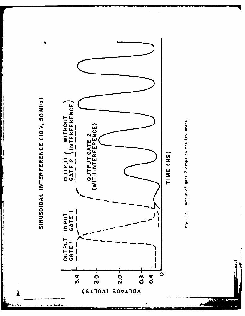
The frequency of the interferer is reduced to 50 MHz in Fig. 17 while
the amplitude is again set at 10 Volts. An even longer transition period
ensues. Now the output, which should remain HIGH, periodically drops to
the LOW state which extends below 0.8 Volts. Obviously, if the output is
sampled while it is in the LOW state, a logic error will result.
In those applications where the output of gate 2 would be differenti-
ated in order to provide a triggering pulse for another stage, the distor-
tion in the leading edge of the responses shown in Figs. 15, 16, and 17
could also cause the generation of logic errors.
A very interesting case is depicted in Fig. 18. Here the amplitude
of the interferer is 20 Volts while its frequency is 100 MHz. Now the
output of gate 2 never makes the transition from the LOW state to the HIGH
state. This will result in a logic error irrespective of the time at which
the output is sampled.
Calcomp plots for the cases illustrated by the sketches shown in
Figures 14-18 are presented in Appendix A.
In some situations it may be desirable to model the interference as
.4
4 .,

36
being inserted in parallel, as opposed to in series, with the output
of gate 1. Several runs were made with the interference source
connected from the output of gate 1 to ground. A large capacitor was
placed in series with the source so as not to upset the dc behavior
of the gate. Results similar to those presented in Figs. 15 through
18 were observed.
A _____

wu 37
zw
-U-
ccJ
zz
o z
:14
I' c
z 0 0
a..
000
IJJ - 0
(SIIOA)30V110
38
Nw
0 z
in -w4-
Owl 21
~I-J - wr__ 0Lii a . <.
Ir D 0%- $
4.14
boz-*m 04
Cl) -I0
Cl)m :)w-
zI-II
.0op0
000
(SIIOA) 3!0V110A

39
0 W
cc w
('.1 w 4J
w z zcc 0 - 40
w~ IL 3 .WLA. 14
0w1 _
-
(44~m1 0
a. No 4-.00 omv woo ow
0
(SIIOA) 3OV110A

40
6. DEFINITIONS OF WAVEFORM PARAMETERS FORDESCRIBING INTERFERENCE EFFECTS.
In order to describe the waveform distortions illustrated in
Section 5, it is convenient to distinguish between steady-state and
transient effects. The steady-state effects pertain to the periodic
portion of the waveform as it tries to maintain a constant output in
the HIGH state. The transient effects apply to the leading edge of
the waveform where it attempts to switch from the LOW to HIGH state.
Various waveform parameters are defined in this section in order to
describe these effects. These parameters are then plotted in Section 7
as a function of the amplitude and frequency of the sinusoidal inter-
ferer.
We first define the steady-state parameters. Because the inter-
ference is periodic, the fluctuations in the output of gate 2 eventually
become periodic. The steady-state parameters are defined with respect
to the periodic portion of the output.
Consider one period of the steady-state output as shown in
Fig. 19. Let
T -
f
denote the period where f is the frequency of the interferer. During
this period let the time spent in the LOW state be denoted by I. The
ERRONEOUS state duty cycle is defined by
D1 T
Note that D1 gives the fraction of a period the waveform resides in
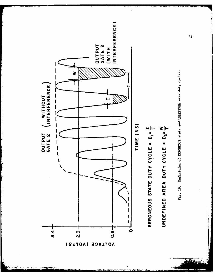
wuzwi 41w
w0
IL)L
z 00 0
w id
0 w
OL
c'-
z
9L W
o~w
m SI
0 0z
0 0
i- z-**4**
(SIIOA)) 49I'

42
t-he LOW state. Similarly, let the time during one period spent in
the UNDEFINED area or below be denoted by W. The UNDEFINED area duty
cycle is defined by
DW2 T'
Note that D2 gives the fraction of a period the waveform resides in
or below the UNDEFINED area.
Two additional parameters for describing the steady-state portion
of the output are the steady-state mean voltage and the steady-state
r.m.s. deviation. Denote the steady-state portion of the output
waveform by vo(t). The steady-state mean voltage is defined to be
T
A- v (t)dtT 0
where the average is over one period of the steady-state portion of
the output. Obviously, the steady-state mean voltage gives the mean
value of the output in the steady-state. The steady-state r.m.s.
deviation is defined to be
T
ami I [v(t) - A]2dt]./2.T
0
Once again, the average is over one period of the steady-state portion
of the output. The steady-state r.m.s. deviation is a measure of the size
of the fluctuations about the steady-state mean voltage.
The transient waveform parameters are now defined. A typical
distorted output is shown in Fig. 20. The time instants t , t2, t3
L

43
z
44 00
z '44
00a 0 0
4) 00414 4.-H. 4.1
0 d
O.0 0
0 X.
0 0 co04 4. 0 0
Dt I
o 0 4.'
$4 41 -. 1w3 0 044 4o4 0
__~C -H 4 3
41 a 4 14 a 17 4 ..
0 F4 04.1$4. 0 440 4 044 w .0 0 44
__ 1 > GJ;o0 P
I ~ ~ 0 0 4I 4.
4-I o 0 00~~~ 44044 31
0- 00D
*1.
*SIA 31 0V110A1e
44
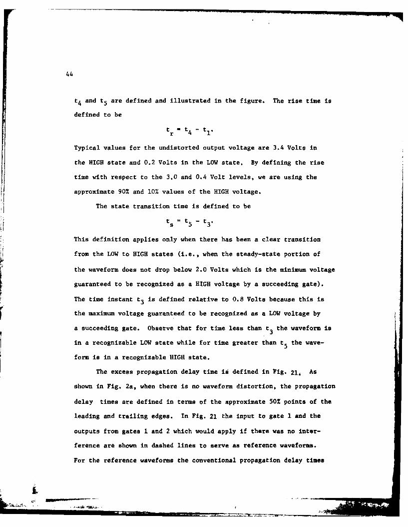
t4 and t5 are defined and illustrated in the figure. The rise time is
defined to be
tr = t4 - tI .
Typical values for the undistorted output voltage are 3.4 Volts in
the HIGH state and 0.2 Volts in the LOW state. By defining the rise
time with respect to the 3.0 and 0.4 Volt levels, we are using the
approximate 90% and 10% values of the HIGH voltage.
The state transition time is defined to be
t s = t - t5 5 3'
This definition applies only when there has been a clear transition
from the LOW to HIGH states (i.e., when the steady-state portion of
the waveform does not drop below 2.0 Volts which is the minimum voltage
guaranteed to be recognized as a HIGH voltage by a succeeding gate).
The time instant t3 is defined relative to 0.8 Volts because this is
the maximum voltage guaranteed to be recognized as a LOW voltage by
a succeeding gate. Observe that for time less than t3 the waveform is
in a recognizable LOW state while for time greater than t5 the wave-
form is in a recognizable HIGH state.
The excess propagation delay time is defined in Fig. 21, As
shown in Fig. 2a, when there is no waveform distortion, the propagation
delay times are defined in terms of the approximate 50% points of the
leading and trailing edges. In Fig. 21 the input to gate 1 and the
outputs from gates 1 and 2 which would apply if there was no inter-
ference are shown in dashed lines to serve as reference waveforms.
For the reference waveforms the conventional propagation delay times

LU 45
tz WLU.
1- -
5- 0
0 w 0
I-L
ULU
0
0 00
-
-. -
(S.L1OA) 30V1O0A

46
are given by
t pd(HL) - T 1- T 0 (first gate)
and
t pd(LH) - T 4- T l* (second gate)
With interference the output of gate 2 may be heavily distorted.
To assist in determin'ilg an eu-ems propagation delay time, the straight
line AB is drawn between the points A and B, as shown in Fig. 21. The
time instants t 2 and t 4 are defined in Fig. 20. t 2 is the last time
the waveform equals 0.4 Volts before reaching 3.0 Volts for the
first time and t4is the first time the waveform equals 3.0 Volts.
T 2is defined to be the time instant at which the straight line AB
reaches the 50% point of the unperturbed gate 2 output. The excess
propagation delay time is then defined to be
t pd (LH) - T 2 - T 4 T T2 - T 0 - (T 1-T 0) (T 4-T 1
T 2 - T0 - tpd (HL) - t pd (LH).

47
7. RESULTS OF COMPUTER SIMULATION
As illustrated in Section 5, the output waveform of gate 2 can
be severely distorted when sinusoidal interference is inserted in
series with the output of gate 1. Several waveform parameters were
defined in Section 6 to assist in describing the interference effects.
The results of our computer simulation are now summarized in terms
of these waveform parameters. A sample program is shown in Appendix B.
The UNDEFINED area duty cycle and the ERRONEOUS state duty cycle
of the gate 2 output are plotted, as a function of interference frequency
with the interferer amplitude as a parameter, in Figures 22 and 23,
respectively. For a constant frequency the duty cycles are seen to
increase with increasing amplitude of the interferer. An interesting
phenomenon is the "resonance effect" which is observed for frequencies
between 30 and 100 MHz. Also, as was implied by Fig. 18, a duty cycle
of 1.0 is possible for sufficiently strong interferers.
The steady-state mean voltage and the steady-state r.m.s. devia-
tion of the gate 1 output are plotted in Figures 24 and 25, respectively.
The gate 1 output is chosen in order to compare with the steady-state
dc results from the McDonnell Douglas study [1]. Although an exact
comparison is not possible because McDonnell Douglas injected the
interference in parallel with the gate 1 output where we inserted the
interference in series with the gate 1 output, the general trends of
the results are identical. Without interference the gate 1 output

48
1.0-
0.9-
0.8-V
LEGEND
0.7- v 0 Ivw a 2.0OV
-J =2.5 V*3.0 V
0.6- 0 4.5 V+ 8.0 v
0.5 13V
x 16 V
20.4- - ~w 9
a a
lITERFERENCE FREQUENCY (MHz)
Fig. 22. UNDEFINED area duty cycle for gate 2 output.

49
1.0-Vt
0.9-
0.8 -LEGEND
1 .5 Va2.0OV
0.7 -2.5 V~*3.OV
U0 4.5 V
cc +. 0 v0.6 - OD 12V
U / 4 13V4 I 15V
In /x 16V
0.1 A. 10 cc 17V
000I0.4+ENEFRQENY-Mz
Fig 23+ROEU tt uyccefrgt upt

50
oo > t i
80I _
+ N+7! 4)40
/ 0wi 0
£44.1'-
'..
ci
*I.-le
In to
(S.LIOA) idjn I 1O 0 DIO VV LISAGV3.LS

51
c, tnco >> >> >
-J0
at
00

52
should remain LOW in the steady-state. It is interesting to note that,
in some cases, even when the steady-state dc value of gate 1 increased
to levels greater than 2.0 volts, gate 2 did not recognize the wave-
form as a HIGH voltage input due to the fluctuations in the waveform.
The steady-state mean voltage and the steady-state r.m.s. devia-
tion of the gate 2 output are plotted in Figures 26 and 27, respec-
tively. Observe that a "resonance effect" is seen in Fig. 26 that does not
appear for the gate 1 output curves shown in Fig. 24. Also, by com-
paring Fig. 27 with Fig. 25, it is seen that the steady-state r.m.s.
deviation of the gate 2 output is much less dependent on amplitude
than is that of the gate 1 output.
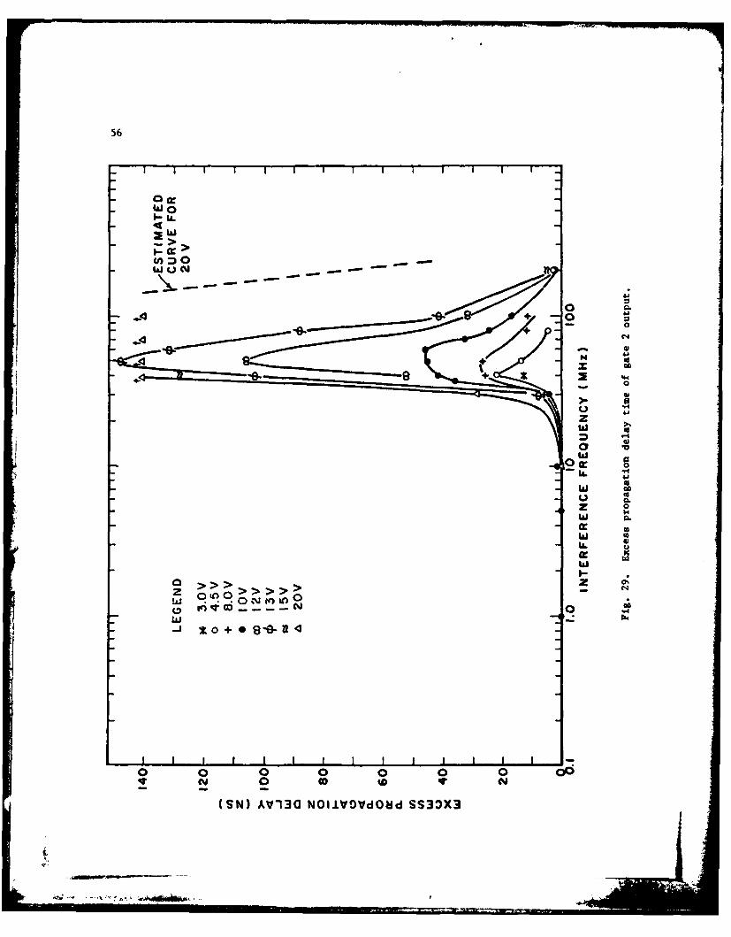
The rise time and excess propagation delay time of the gate 2
output are plotted in Figures 28 and 29, respectively. The plots are
functions of the interference frequency with interference amplitude
as a parameter. Observe that, for large enough amplitudes and for
frequencies in the range of 30 to 100 MHz, the "resonance effect" is
seen once again. Rise times and excess propagation delay times in
excess of 100 nanoseconds apply during this "resonance" phenomenon.
These values are an order of magnitude larger than the typical values
without interference.
It should be pointed out that the sinusoidal interference dis-
torts the trailing edge of the gate 2 output in a manner different
from its effect on the leading edge. Therefore, a plot of the fall
time differs from the rise time plot of Fig. 28. The effect of the
phase of the interfering signal on the rise and delay times was also

53
ILl-J *0o+e9-9 <
00
4)
44
06
wu 0z>w r
4'4'
w rIi. 4)
In OWCY 4'
(S.IOA inino31V JO30110 NVW 3VISAOV.w

54
I I>>>
/ot
%4-
4O 1
o >z- '
wa
II
z
0 0 I
In cl 0 cWdI
(SIIA) idin 31V .4 N01VIA0 SN 31IS AV31

55
wUcJ
woo
+ 00
tie
*4
C.4
0..
00
0~ 0
q0
56
(flO
;7 > >
me. 0
0
0
z c
w
-4
w
U)U
w Pk4
oa +
0 0 0 0I0.CY 0co 4 IV
(SN)AV13 N~lV9Vdkld S33X

57
investigated. It was determined that the phase had no noticeable
effect on the rise time but did introduce changes in the delay time
by an amount as large as one period of the interfering signal.
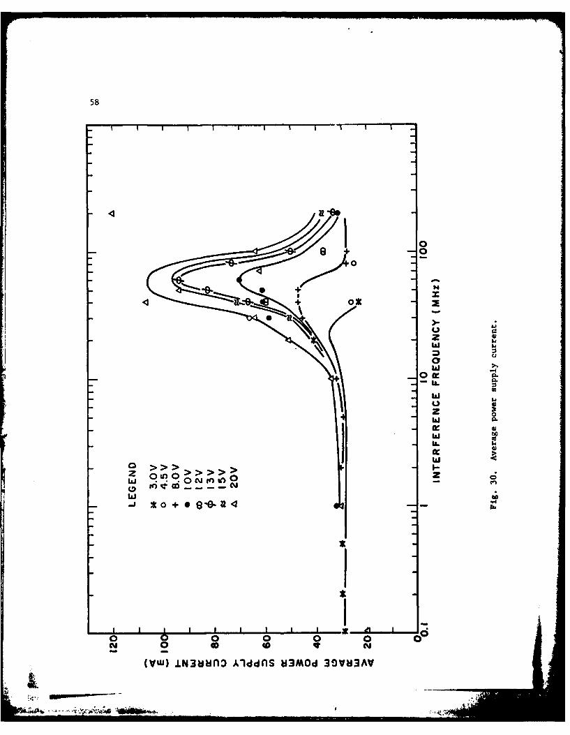
The average power supply current is plotted in Fig. 30. Notice
that the average current drain on the power supply may increase sig-
nificantly in the "resonance" region which, once again, extends from
30 to 100 MHz.
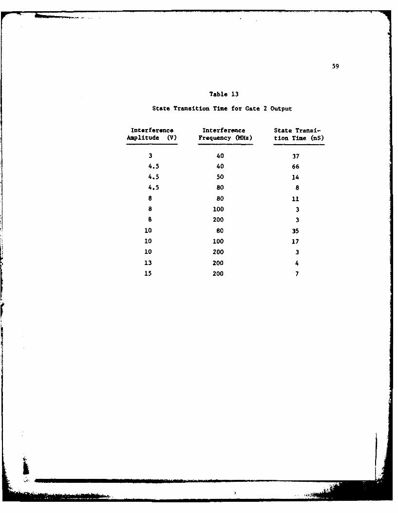
Some state transition times are tabulated in Table 13 for
various cases where a clear transition was made from LOW to HIGH
states. As with the rise time and excess propagation delay time,
values of the state transition time can be relatively large compared
to typical rise and propagation delay times.
Finally, a calculation was made of the average power delivered
by the interference source. This was accomplished by first multi-
plying the instantaneous voltage and instantaneous current of the
interference source, in order to obtain the instantaneous power de-
livered by the source, and then averaging the result. The average
delivered powers for interference amplitudes of 0.5V and 20V were
1.4 mW and 540 mW, respectively. This range corresponds to the same
range of absorbed power measured by McDonnell Douglas in their
experimental study [1].
58
0-0
zw
w
w
(WWww
*0 +
0 0 0
CY 0 0 0 $ w
(V VU) ±N3&ibnf Alddfls JMOd* 3VI3AV
59
Table 13
State Transition Time for Gate 2 Output
Interference Interference State Transi-Amplitude (V) Frequency (MHz) tion Time (nS)
3 40 37
4.5 40 66
4.5 50 14
4.5 80 8
8 80 11
8 100 3
8 200 3
10 80 35
10 100 17
10 200 3
13 200 4
15 200 7

60
8. SUMMARY AND SUGGESTIONS FOR FUTURE WORK
This work has emphasized EMI upset in an integrated circuit 7400 TTL
NAND gate due to sinusoidal interference injected in series with the
gate output. Severe waveform distortions, capable of causing serious
logic errors, were observed through computer simulation of the digital
circuits involved. These results are in sharp contrast to the pure
dc offsets reported by McDonnell Douglas [1]. We conclude that RF
interference can pose a serious threat to the successful operation of
digital circuits.
The work reported herein is merely a small step forward towards
understanding interference effects in digital equipments. As far as
the 7400 TTL NAND gate is concerned, it is desirable to study in
greater depth the consequences of interference in the power line and
ground connections. Also, other interference waveforms, such as pulses
and spiked transients, should be investigated.
The 7400 TTL NAND gate represents merely a single technology and
a single type of digital circuit. Other types of technologies, such
as ECL, CMOS, and IlL, need to be studied. Also, the commonality be-
tween the NAND gate and other logic circuits, such as OR, AND, and NOT
gates, should be pursued.
It would be highly desirable to model the various logic gates
in terms of circuits containing considerably fewer semiconductor de-
vices. This may be possible using the macromodel concept which has
been successful in generating relatively simple circuit models for
Jf w

61
operational amplifiers. Once simpler models have been devised, it
would be desirable to combine them in an effort to model more compli-
cated combinations of logic circuits. In this way, it may be possible
to arrive at EfI performance curves for relatively sophisticated
digital equipments.
Finally, all of the above should be supplemented by an experi-
mental effort in order to validate analytical and computer simulation
results.
. ... ..£ . :
.. . .. I , . .. . .... .1- e J
S _ ii i ,, " ,
62
REFERENCES
1. "Integrated Circuit Electromagnetic Susceptibility Handbook,"Report MDC E 1929, 1 August 1978, McDonnell-Douglas Company.
2. "User's Guide for SPICE," Electronic Research Laboratory,College of Engineering, University of California, Berkeley.
3. "Digital Integrated Electronics," H. Taub and D. Schilling,(McGraw-Hill, 1977).

63
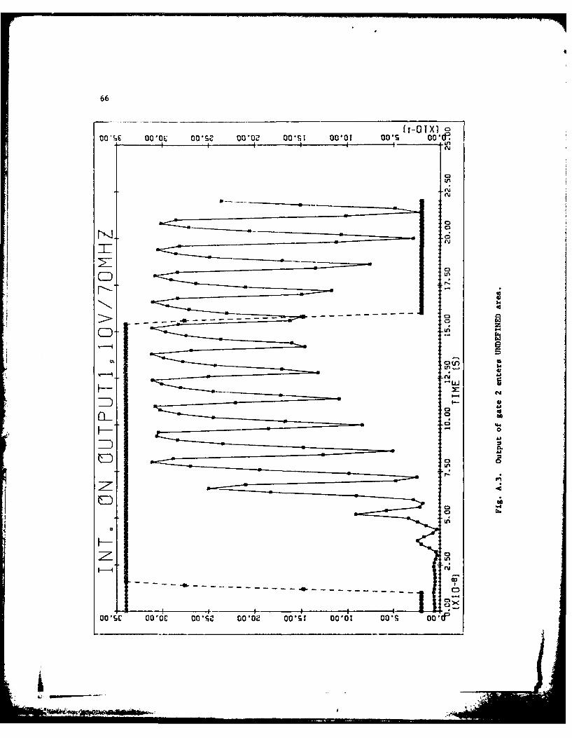
APPENDIX A: CALCOMP PLOTS OF REPRESENTATIVE OUTPUT WAVEFORMS
The Calcomp plots corresponding to the waveforms sketched
in Figures 14-18 are presented in Figures A.1 - A.5. However, as
defined in Fig. 9, the transition from the fourth to first quarters
is shown in addition to the transition from the third to fourth
quarters. In Fig. A.1 the two inputs to gate 1, the output of gate
1, and the output of gate 2 are plotted while in Figures A.2 - A.5
only the two inputs to gate 1 and the output of gate 2 are plotted.
As indicated on the plots, the vertical voltage scale is mul-
tiplied by 101 while the horizontal time scale is multiplied by 108.
The sketches shown in Figures 14-18 are seen to capture the essen-
tial features of the Calcomp plots. In addition, it is seen that
the leading edge of the gate 2 output, corresponding to the transi-
tion from the third to fourth quarters, differs markedly from the
trailing edge of the gate 2 output, corresponding to the transition
from the fourth to first quarters.
Ii

64 ________
(T-OIXI t
co ?l 0 1C 0 1tic 011 l oI I 00a 001 c
C,
SIC34VGA
Jh X
- -- - - I..G
-- - - - - - - - -. - -- 4cJ
00 a 001C 0 ,01 0 1Tie 0'e 00'l u, a o-4

65
~ QQO~ OO~1 001 0
CO'Ge OWNOcl
Li"
il
o to
0
.44CD-r
zS-0--------------------------- -0------------------------------------3
co -sr, -WOL on ,.;z o 01 02 0 0,0. .. .......
66
00 sc 0 oo Dolse 00,02 DOI~ 1 0,1 Do oo -d
C3
CD0
71___ _ -0 - - - - -C
C3
1-4
0~J)
0 U0ry- --- -
Em1s 000 0.zDle 0*Ct 0,1 D, c

67
OOSGE 0010C 0OOe OU 00'S? 00,01 DO'S 0
0
Cu
00
00
oi
C3 0
00
0
-4 1 ------
00 o 001T 0 11)1 0 S 0 -d

68
'1; OMIOL 00o1-e O0~ 0'0 0sr o r
CD
-
01
14t
CD
010* 00101..

I69
APPENDIX B: SAMPLE SPICE COMPUTER PROGRAM
1)TRANSIENT ANALYS5IS OF HND GATE
2 *3)* RESISTORS4)Rl 2 9 4.38K5)R2 9 4 1.43m6)R3 9 6 0.116K7)R4 5 0 1.03"8)* DIODES9.DIN1 0 1 STAN
10DZ1l12 0 10 STAN.1 11)D3 7 8 V20312 * TRANSISTORS13)011 3 2 1 TRi14)012 3 2 10 TRJ
15)02 4 3 5::16)03 6 4 7 TR3
17)04 8 5 0 R19)* DESCRIPTION OF LOAD STAGEl9)* RESISTORS
20)R5 9 13 0.438"21)R6 9 15 0.143"22)R7 9 17 0.0116K23)P:8 16 22 0.106K24)2 DIODES25)DIIN4 22 11 STAHL
26)DIN5 22 12 STAHL27)06 18 19 D103L28 *TRAUSISTORS29)051 14 13 11 TRIL30)052 14 13 12 TRIL31)06 15 14 16 TR2L32)07 17 15 18 TR3L33)08 19 16 22 TR4L34)2 LOAD RESISTOR AND CAPACITOR FOR LOAD STAGE WITH FAN OUT JU
35)a WITH LOAD TIED TO SROUND
363* LOAD RESISTOR37)RLL 23 22 0.4"39)* LOAD CAPACITOR39)CLL 23 22 15PP40'* MODEL CARDS FOR DIODES AND TRANSISTORS OF FIRST STAGE41).MDLSA D(Rs=600HMS TT=0.jNS CJO=2PF PB=0.6V BV=40v Is=1E.-16)42.,MODEL Dx03 D(Rs=300Hms TT=Q.jNs cJO=2FF PDO0.6v sv=40v IS51E-16)
43).400EL TRi 1PN(DF=0.316 DRO0.02 RI.=68OHMS TF=0.39N5 TR100NHS RC=jQOHMSI
44)+RE=1OHH vA=200v c2=1000 C4=1 CCS=2PF CJE1IPF PEO0.7v E=0.33j 45)+CJC=0.5FF PC=0.5V mc=0.33 KF=6,6E-16)
46*NMODEL TR2 tPH(BF=19.8 DRO0.06 RV=750HMS TF=0.39NS TR=jQQNS
47)+RE=jOHm VA=200V vs=200v C2=1000 C4=1 cs=2PF CJE=2PF PE=0.7v mE=0.33489+CJC=JPF PC=0.5v mc=.33 KF=6.6E-16 xs=1E-16)49,.MODEL TR3 HPNvBF=17.2 BRrn.082 RB=70OHms RC=JOOHMS TF=Q*39NH"*1u'
50,,RE=1OHmm vA=200v C2=1000 c4=1 ccs=2PF cJE=2PF PE=0.7V mEO0.3351)+CJC=1PF PC=0,5V MCO0.33 KF=6.6E-16 IS=1E-16)
52,.MODEL TR4 NPN(*F=21.7 R=0.106 RB=SQOHmS RC=100H45 TFO0.39NS TR=100Nb53)+RE=1ONm VA5200v vs=200V C2=1000 C4=1 CCS=2PF cJE2PP PE=0.7v mE=0.33
54,,CJC=IPF PC=O.Sv mc=0.33 KF=6.6E-16 Is=1E-16)
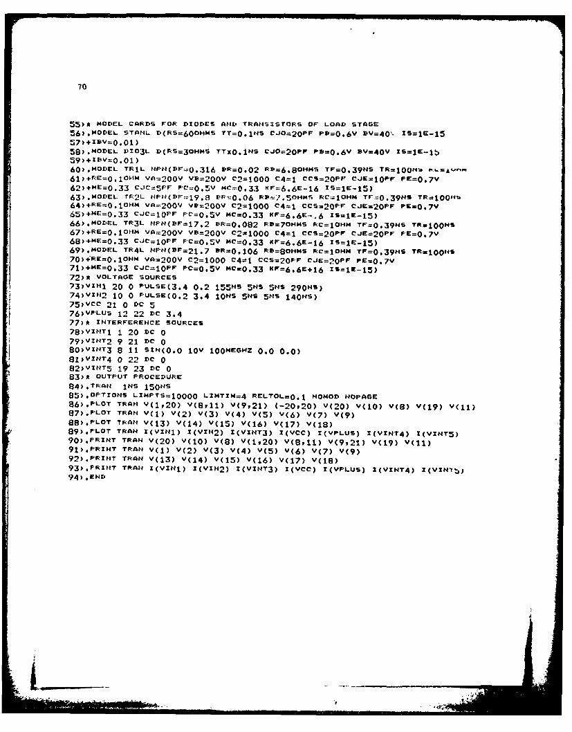
70
55.* MODEL CARDS F DIODES AUL. TRANSISTORS OF LOAD STAGE56).MODEL STAtNL D(RS=60OHiMS TT0O.eS cJO=20PV P9=0.6v I'v=40, xs1IE-1557)+4v=0.01)592 9 MOLEL P10Z3L D(RS=30M4S T~xO.1MS cJO=2OPF P9=0.6v sv=40V ZS=1E-1b59) +ID v0. 01)60) *MODEL TR1L NPNEIF..a.316 BR=O.O2 P.L=6.BOHMS TF=Q*391NS Tpt~lotqNa KL=~w6Ib+RE=0.jOHM VA=200v vB=200v c210 c4=1 Ccs=2F CJE1IOPF PEO0.7v62*+mE=0.33 cJc=5PF Fc=O.5v tI=0.33 KF=6.6E-16 !51E.15)63) *mOvct rr-2L NPNf(B4F'-j9.6q P''-0.06 Rl%=?.rHM'S RC=1OHM Tr=0.394S TRts100e'4b64)+RE=0.lONm VA=200V VB=200v C2=1000 C4=1 ccs=20PF CJE=20PF PE=0.7V65)+mc=0.33 CJC=jF PC=O.5V MC=Q*33 KF=6.6E-6 zs1Et-15)66).MOrEL TR3L MPH(BD=17.2 BR=0.082 PD=7Omms RC=1OHM TF=0.39HS TRtwjOONS67)+RE=0.JOHM VA=200V vD=200v C2=1000 C4=1 CCS=2OPFP CJE=20PF F*E=Q.7v68)+mE=0.33 CJC1JOPF F"CO.5V mcO.33 KF=6.6E-16 Zs1E-15)69)#MODEL TR4L NPN(BF=21.7 DR=0.106 R9=9OHMS R'C=1ONM TF=O.39u5 TRmlOOeS70)-+E=O.IOHm VA=200V c2=1000 c4=1 CCs=20PF CJE=2OPF PE=0.7v71)+ME=0.33 CJC=jQPF PC=0.Sv mc=033 KF=6-6E+16 xs~lt-15)72)A VOLTAGE SOURCES73)vZImj 20 0 PULSE(3.4 0.2 155HS 15NS 5ms 290"s)74)v!N2 10 0 PULSE(0.2 3.4 IONS Sms 5MS 14O'~s)75)vcc 21 0 Dc 576)VPLUS 12 22 DC 3*477)a INZTERFERENCE SOURCES78,VINTI 1 20 DC 079,VXINT2 9 21 Dc 080,VXINT3 8 11 SZN(0.0 Jby bOOMEGHZ 0.0 0.0)81)VIT4 0 22 Dc 082)V1T5 19 23 LDC 083)* OUTPUT P~ROCEDURE
85),.OPTONS LXMPTS=1oOOO LIMT!m=4 RELTOL=O.l NOMOD HOPAGE* 86>*PLOT TRAMl Y(1,20) V(S,11) V(9,p2l) (-20,20) V(20) V(10) v(S) V(19) V(11)
837).PLOT TRAM V(I) v(2) v(3) V(4) V(5) v(6) V(7) v(9)
89>.PLOT TRAM Z(viml) Z(V11-12) Z(VZNT3) Z(VCC) X(VPLUS) X(VXNT4) I(VINT5)90).PRINT TRAM v(20) V(10) V(8) V(1920) V(8.11) v(9,21) v(19) Y(11)91,.PR1NT TRAM V(J) V(2) V(3) V(4) v(5) V(6) V(7) V(9)92).RIT TRAM v(13) V(14) v(15) V(16) V(17) v(18)93)*FRItlT TRAMl X(VIN1) Z(VIN2) I(VXNT3) Z(vCC) Z(VPLUS) I(VXMT4) Z(VXNTt )94 EMD
MISSIONOf
Rom Air Development CenterRAVC pfrA6 and executeA wLeatchw, devetopvent, tut andAetected acqca.4ition ptogxam6 in,6uppo~lt oj Comma~d, ConttwLConitkom~n and Intettgence (C01) actvitieA. Technri..aIand engineeAing 6uPPOA-t within a~tea& oj techznea comnpetenc~eiA p.tovided to BSV PXog9am OJ&eA MPIS) and othzel ESOetemnent6. The p~incipat techicat mLiA6ion vA'ea6 aLLcommwzi-ationA, et'Ltomanetic. guiAdance and con*Aoto, £WL&-VeillanCe 0, g~tOund and deAoa6pdce object6, iJIteltience datacotteztion and handting, indouation 6yatem tecinotogy,iono.6phevJJ potopagation, 6otid 6a te hienceA, smeoIwephpa. and etetonia utiabiUit, mWL&(flnabdd andacompatibitity.

DAU
IIFILU