Embed Size (px)
Citation preview

WasatchDevices.com Revised 2016-08-26 Page 1
OEM API Specification For Wasatch Photonics OEM Spectrometers

WasatchDevices.com Revised 2016-08-26 Page 2
Revision Log Revision Date By Reason
1.0 2016-08-29 J. Traud Initial Release
Contents General Description ...................................................................................................................................... 3
OEM Connector Pinout ............................................................................................................................. 3
External I/O Control Connector ................................................................................................................ 4
SPI Specification ............................................................................................................................................ 5
UART Specification ........................................................................................................................................ 6
Bluetooth Specification ................................................................................................................................. 6
Packet Organization ...................................................................................................................................... 7
Configuration Get/Set Packet ................................................................................................................... 7
Configuration Set Response Packet .......................................................................................................... 7
Configuration Get Response Packet ......................................................................................................... 7
CRC Calculation ......................................................................................................................................... 8
Data Transmit mode and the Data Packet ................................................................................................ 9
Command Table .......................................................................................................................................... 10
FPGA Configuration Registers ..................................................................................................................... 13
Individual Command Details ....................................................................................................................... 14
FPGA Configuration Register Details ........................................................................................................... 18

WasatchDevices.com Revised 2016-08-26 Page 3
General Description Wasatch Photonics OEM Spectrometers are equipped with various methods of low-level control using
UART, SPI, Bluetooth, and USB.
OEM Connector Pinout OEM spectrometers come equipped with a 14-pin 1.27mm pitch ribbon connector for low-level
commands.
Pinout designations and a color coded breakout by function can be found below.
Pin Description Pin Description
1 SPI_ACQUIRE 2 N/C
3 DATA_READY 4 ACQUIRE
5 GND 6 GND
7 SPI_MISO 8 SPI_CLK
9 SPI_CS 10 SPI_MOSI
11 GND 12 GND
13 UART1_RX 14 UART1_TX
Below are the associated part numbers of the connectors.
Manufacturer Part Number Part Description
3220-14-0200-00 CNC Tech 14-pos Right Angle Connector on WP Raman
3230-14-0101-00 CNC Tech 14-pos Socket Mating ribbon cable connector
WasatchDevices.com Revised 2016-08-26 Page 4
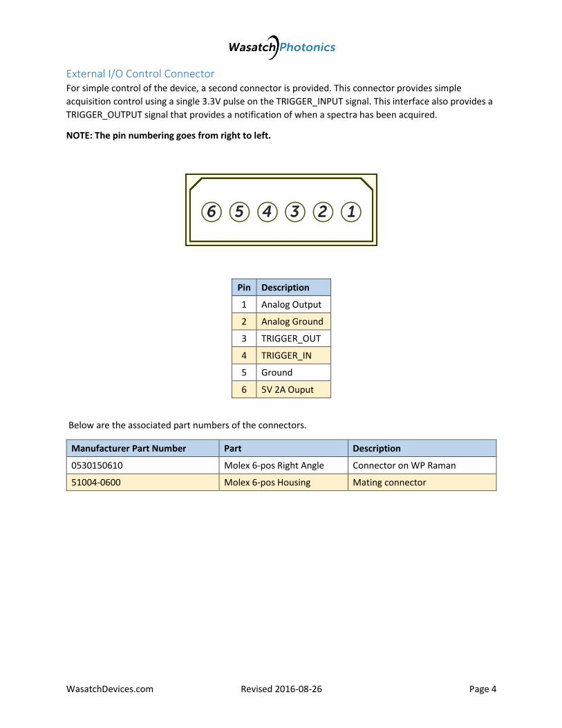
External I/O Control Connector For simple control of the device, a second connector is provided. This connector provides simple
acquisition control using a single 3.3V pulse on the TRIGGER_INPUT signal. This interface also provides a
TRIGGER_OUTPUT signal that provides a notification of when a spectra has been acquired.
NOTE: The pin numbering goes from right to left.
Pin Description
1 Analog Output
2 Analog Ground
3 TRIGGER_OUT
4 TRIGGER_IN
5 Ground
6 5V 2A Ouput
Below are the associated part numbers of the connectors.
Manufacturer Part Number Part Description
0530150610 Molex 6-pos Right Angle Connector on WP Raman
51004-0600 Molex 6-pos Housing Mating connector

WasatchDevices.com Revised 2016-08-26 Page 5
SPI Specification The WP Raman SPI interface is a simple Serial Peripheral Interface (SPI) compatible serial bus configured
as a SLAVE. The bus signals required are a clock input (SCK) plus a separate data input (SI) and data
ouput (SO) lines. Access to the device is controller using a chip select (CS) input signal. Commands and
replys are received and transmitted in 8-bit packets and data is transmitted in 16-bit packets. Both
signals are sent at a 21-MHz clock rate.
The interface supports on Mode 0 (CPOL = 0, CPHA = 0) configuration shown in Figure 1 below. The state
of the SCK signal when the bus master is in Stand-by mode and no data is being transferred is low for
Mode 0. The Serial Data In (SI) is sampled at the rising edge of the Serial Clock (SCK) signal and the Derial
Data Output (SO) is driven after the falling edge of the SCK clock signal.
Figure 1 – SPI Timing
Description Value Units
Maximum voltage on any pin 3.6 V
Maximum low level input 0.8 V
Minimum high level input 2.0 V
Minimum high level ouput 2.9 V
Maximum low level ouput 0.4 V
Maximum CPI clock rate 20 MHz
See OEM Connector Pinout on Page 3 for pin assignment information
WasatchDevices.com Revised 2016-08-26 Page 6
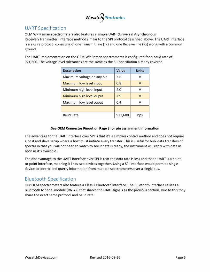
UART Specification OEM WP Raman spectrometers also features a simple UART (Universal Asynchronous
Receiver/Transmitter) interface method similar to the SPI protocol described above. The UART interface
is a 2-wire protocol consisting of one Transmit line (Tx) and one Receive line (Rx) along with a common
ground.
The UART implementation on the OEM WP Raman spectrometer is configured for a baud rate of
921,600. The voltage level tolerances are the same as the SPI specifiation already covered.
Description Value Units
Maximum voltage on any pin 3.6 V
Maximum low level input 0.8 V
Minimum high level input 2.0 V
Minimum high level ouput 2.9 V
Maximum low level ouput 0.4 V
Baud Rate 921,600 bps
See OEM Connector Pinout on Page 3 for pin assignment information
The advantage to the UART interface over SPI is that it’s a simplier control method and does not require
a host and slave setup where a host must initiate every transfer. This is useful for bulk data transfers of
spectra in that you will not need to watch to see if data is ready, the instrument will reply with data as
soon as it’s available.
The disadvantage to the UART interface over SPI is that the data rate is less and that a UART is a point-
to-point interface, meaning it links two devices together. Using a SPI interface would permit a single
device to control and querry information from multiple spectrometers over a single bus.
Bluetooth Specification Our OEM spectrometers also feature a Class 2 Bluetooth interface. The Bluetooth interface utilizes a
Bluetooth to serial module (RN-42) that shares the UART signals as the previous section. Due to this they
share the exact same protocol and baud rate.
WasatchDevices.com Revised 2016-08-26 Page 7
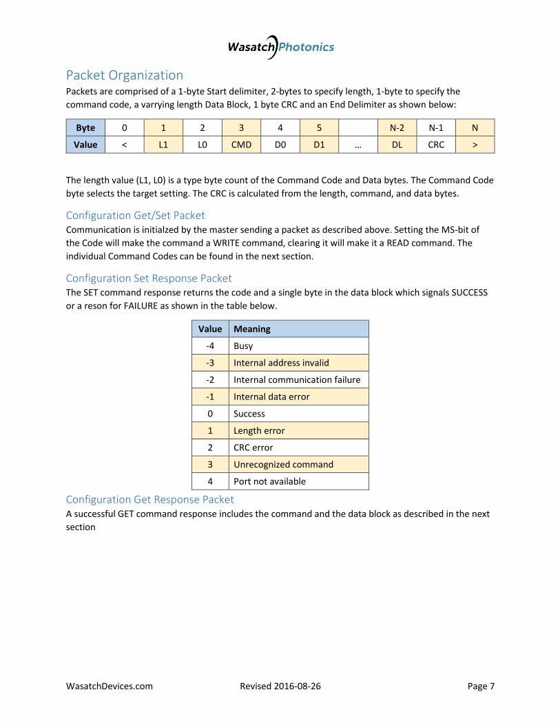
Packet Organization Packets are comprised of a 1-byte Start delimiter, 2-bytes to specify length, 1-byte to specify the
command code, a varrying length Data Block, 1 byte CRC and an End Delimiter as shown below:
Byte 0 1 2 3 4 5 N-2 N-1 N
Value < L1 L0 CMD D0 D1 … DL CRC >
The length value (L1, L0) is a type byte count of the Command Code and Data bytes. The Command Code
byte selects the target setting. The CRC is calculated from the length, command, and data bytes.
Configuration Get/Set Packet Communication is initialzed by the master sending a packet as described above. Setting the MS-bit of
the Code will make the command a WRITE command, clearing it will make it a READ command. The
individual Command Codes can be found in the next section.
Configuration Set Response Packet The SET command response returns the code and a single byte in the data block which signals SUCCESS
or a reson for FAILURE as shown in the table below.
Value Meaning
-4 Busy
-3 Internal address invalid
-2 Internal communication failure
-1 Internal data error
0 Success
1 Length error
2 CRC error
3 Unrecognized command
4 Port not available
Configuration Get Response Packet A successful GET command response includes the command and the data block as described in the next
section
WasatchDevices.com Revised 2016-08-26 Page 8
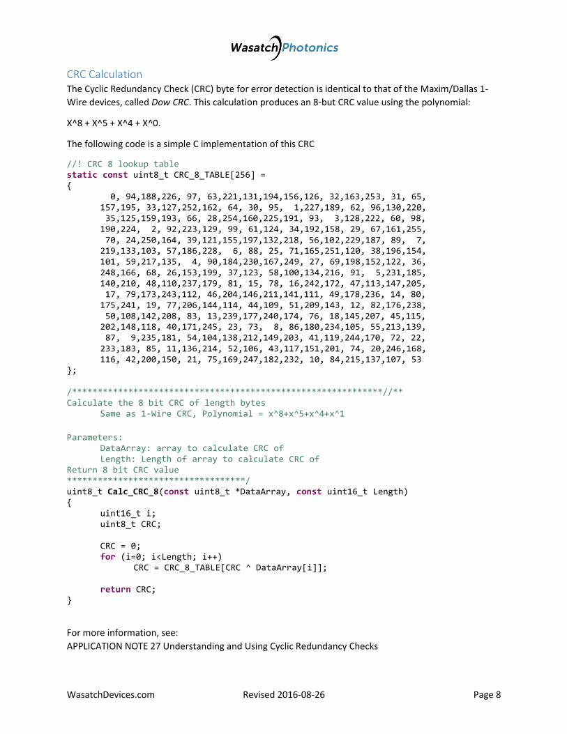
CRC Calculation The Cyclic Redundancy Check (CRC) byte for error detection is identical to that of the Maxim/Dallas 1-
Wire devices, called Dow CRC. This calculation produces an 8-but CRC value using the polynomial:
X^8 + X^5 + X^4 + X^0.
The following code is a simple C implementation of this CRC
//! CRC 8 lookup table static const uint8_t CRC_8_TABLE[256] = { 0, 94,188,226, 97, 63,221,131,194,156,126, 32,163,253, 31, 65, 157,195, 33,127,252,162, 64, 30, 95, 1,227,189, 62, 96,130,220, 35,125,159,193, 66, 28,254,160,225,191, 93, 3,128,222, 60, 98, 190,224, 2, 92,223,129, 99, 61,124, 34,192,158, 29, 67,161,255, 70, 24,250,164, 39,121,155,197,132,218, 56,102,229,187, 89, 7, 219,133,103, 57,186,228, 6, 88, 25, 71,165,251,120, 38,196,154, 101, 59,217,135, 4, 90,184,230,167,249, 27, 69,198,152,122, 36, 248,166, 68, 26,153,199, 37,123, 58,100,134,216, 91, 5,231,185, 140,210, 48,110,237,179, 81, 15, 78, 16,242,172, 47,113,147,205, 17, 79,173,243,112, 46,204,146,211,141,111, 49,178,236, 14, 80, 175,241, 19, 77,206,144,114, 44,109, 51,209,143, 12, 82,176,238, 50,108,142,208, 83, 13,239,177,240,174, 76, 18,145,207, 45,115, 202,148,118, 40,171,245, 23, 73, 8, 86,180,234,105, 55,213,139, 87, 9,235,181, 54,104,138,212,149,203, 41,119,244,170, 72, 22, 233,183, 85, 11,136,214, 52,106, 43,117,151,201, 74, 20,246,168, 116, 42,200,150, 21, 75,169,247,182,232, 10, 84,215,137,107, 53 }; /*************************************************************//** Calculate the 8 bit CRC of length bytes Same as 1-Wire CRC, Polynomial = x^8+x^5+x^4+x^1 Parameters: DataArray: array to calculate CRC of Length: Length of array to calculate CRC of Return 8 bit CRC value ***********************************/ uint8_t Calc_CRC_8(const uint8_t *DataArray, const uint16_t Length) { uint16_t i; uint8_t CRC; CRC = 0; for (i=0; i<Length; i++) CRC = CRC_8_TABLE[CRC ^ DataArray[i]]; return CRC; }
For more information, see:
APPLICATION NOTE 27 Understanding and Using Cyclic Redundancy Checks

WasatchDevices.com Revised 2016-08-26 Page 9
Data Transmit mode and the Data Packet After an acquire signal is sent and when the data is ready to send and the Data Ready pin will go high.
Then the SPI port will automatically switch from Command Mode to Data Transmit Mode.
In Data Transmit Mode the SPI bus is setup to send 16-bit words, one for each data point. Only data is
sent, none of the other information such as delimiters, length, or CRC are included. Each data point is
sent out with each 16 clock cycles. When all of the data points are transmitted (eitehr 1024, 1044, or
2048 depending on sensor configuration) the Data Ready pin will go LOW and the SPI port will switch
back to Command Mode.
WasatchDevices.com Revised 2016-08-26 Page 10
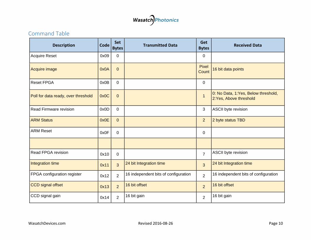
Command Table
Description Code Set
Bytes Transmitted Data
Get Bytes
Received Data
Acquire Reset 0x09 0 0
Acquire image 0x0A 0 Pixel
Count 16 bit data points
Reset FPGA 0x0B 0 0
Poll for data ready, over threshold 0x0C 0 1 0: No Data, 1:Yes, Below threshold,
2:Yes, Above threshold
Read Firmware revision 0x0D 0 3 ASCII byte revision
ARM Status 0x0E 0 2 2 byte status TBD
ARM Reset 0x0F 0 0
Read FPGA revision 0x10 0 7 ASCII byte revision
Integration time 0x11 3 24 bit Integration time 3 24 bit Integration time
FPGA configuration register 0x12 2 16 independent bits of configuration 2 16 independent bits of configuration
CCD signal offset 0x13 2 16 bit offset 2 16 bit offset
CCD signal gain 0x14 2 16 bit gain 2 16 bit gain
WasatchDevices.com Revised 2016-08-26 Page 11
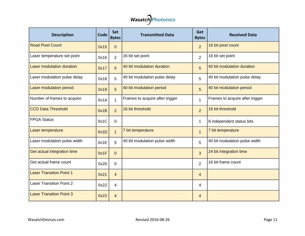
Description Code Set
Bytes Transmitted Data
Get Bytes
Received Data
Read Pixel Count 0x15 0 2 16 bit pixel count
Laser temperature set point 0x16 2 16 bit set point 2 16 bit set point
Laser modulation duration 0x17 5 40 bit modulation duration 5 40 bit modulation duration
Laser modulation pulse delay 0x18 5 40 bit modulation pulse delay 5 40 bit modulation pulse delay
Laser modulation period 0x19 5 40 bit modulation period 5 40 bit modulation period
Number of frames to acquire 0x1A 1 Frames to acquire after trigger 1 Frames to acquire after trigger
CCD Data Threshold 0x1B 2 16 bit threshold 2 16 bit threshold
FPGA Status 0x1C 0 1 8 independent status bits
Laser temperature 0x1D 1 7 bit temperature 1 7 bit temperature
Laser modulation pulse width 0x1E 5 40 bit modulation pulse width 5 40 bit modulation pulse width
Get actual integration time 0x1F 0 3 24 bit integration time
Get actual frame count 0x20 0 2 16 bit frame count
Laser Transition Point 1 0x21 4 4
Laser Transition Point 2 0x22 4 4
Laser Transition Point 3 0x23 4 4
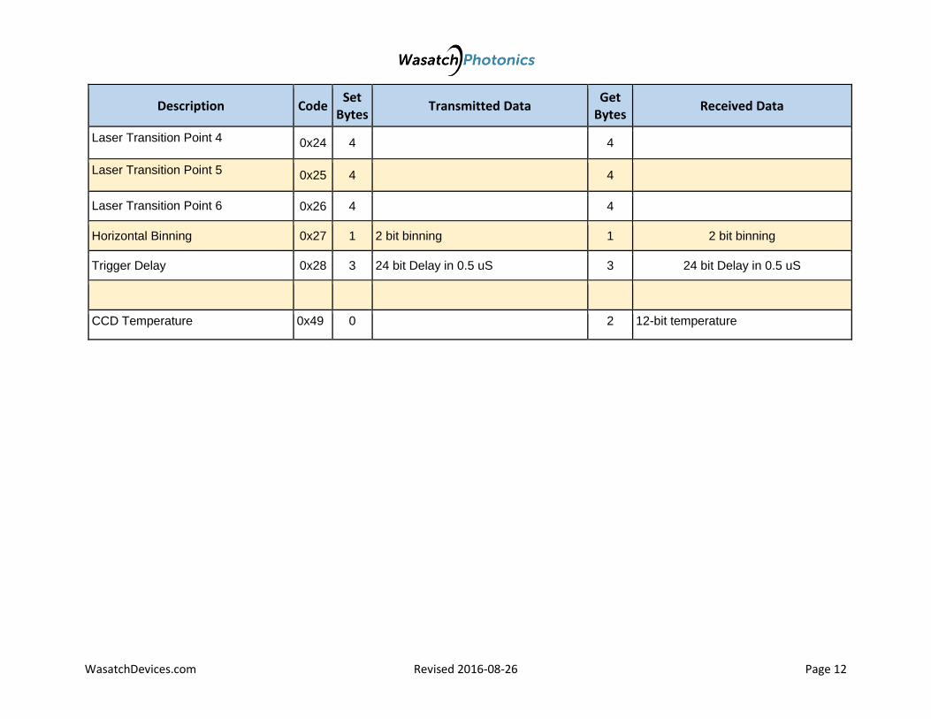
WasatchDevices.com Revised 2016-08-26 Page 12
Description Code Set
Bytes Transmitted Data
Get Bytes
Received Data
Laser Transition Point 4 0x24 4 4
Laser Transition Point 5 0x25 4 4
Laser Transition Point 6 0x26 4 4
Horizontal Binning 0x27 1 2 bit binning 1 2 bit binning
Trigger Delay 0x28 3 24 bit Delay in 0.5 uS 3 24 bit Delay in 0.5 uS
CCD Temperature 0x49 0 2 12-bit temperature
WasatchDevices.com Revised 2016-08-26 Page 13
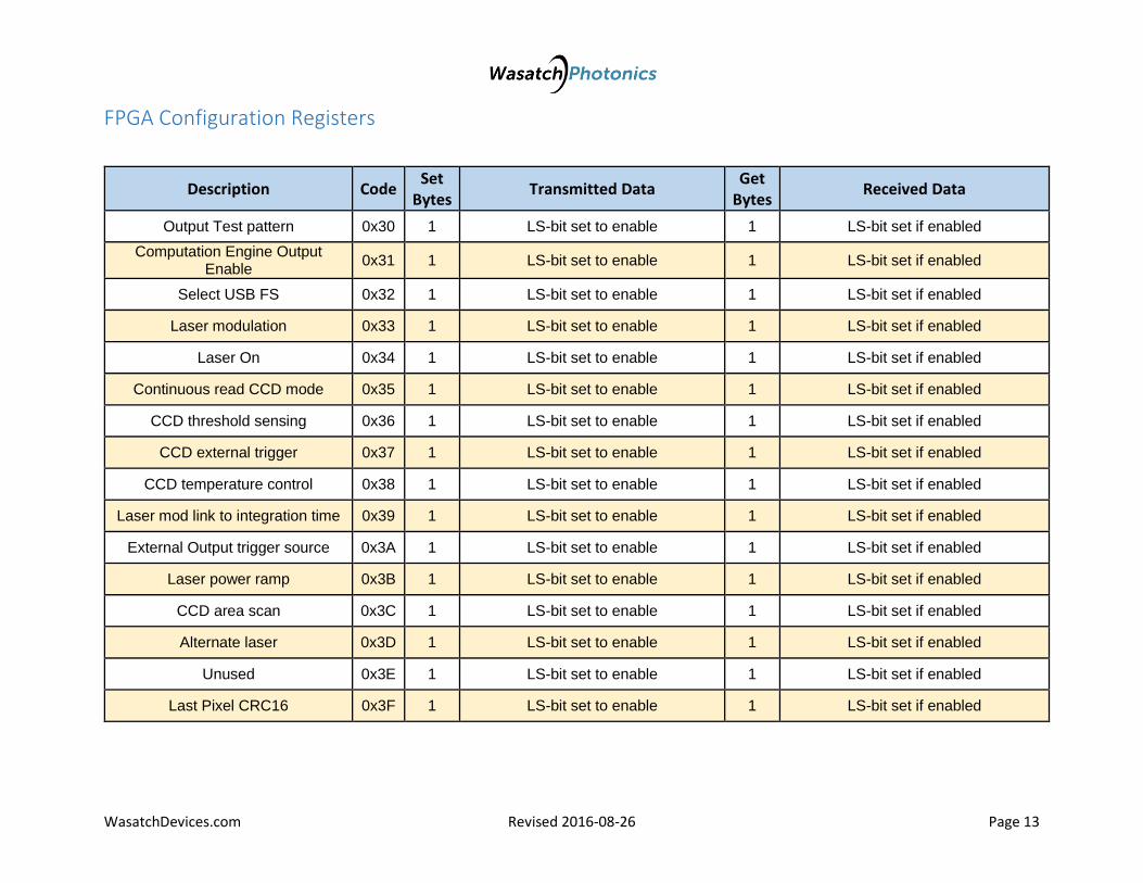
FPGA Configuration Registers
Description Code Set
Bytes Transmitted Data
Get Bytes
Received Data
Output Test pattern 0x30 1 LS-bit set to enable 1 LS-bit set if enabled
Computation Engine Output Enable
0x31 1 LS-bit set to enable 1 LS-bit set if enabled
Select USB FS 0x32 1 LS-bit set to enable 1 LS-bit set if enabled
Laser modulation 0x33 1 LS-bit set to enable 1 LS-bit set if enabled
Laser On 0x34 1 LS-bit set to enable 1 LS-bit set if enabled
Continuous read CCD mode 0x35 1 LS-bit set to enable 1 LS-bit set if enabled
CCD threshold sensing 0x36 1 LS-bit set to enable 1 LS-bit set if enabled
CCD external trigger 0x37 1 LS-bit set to enable 1 LS-bit set if enabled
CCD temperature control 0x38 1 LS-bit set to enable 1 LS-bit set if enabled
Laser mod link to integration time 0x39 1 LS-bit set to enable 1 LS-bit set if enabled
External Output trigger source 0x3A 1 LS-bit set to enable 1 LS-bit set if enabled
Laser power ramp 0x3B 1 LS-bit set to enable 1 LS-bit set if enabled
CCD area scan 0x3C 1 LS-bit set to enable 1 LS-bit set if enabled
Alternate laser 0x3D 1 LS-bit set to enable 1 LS-bit set if enabled
Unused 0x3E 1 LS-bit set to enable 1 LS-bit set if enabled
Last Pixel CRC16 0x3F 1 LS-bit set to enable 1 LS-bit set if enabled
WasatchDevices.com Revised 2016-08-26 Page 14
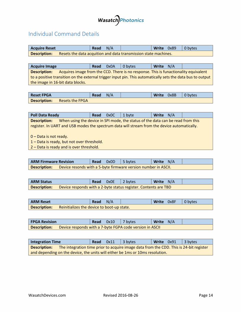
Individual Command Details
Acquire Reset Read N/A Write 0x89 0 bytes
Description: Resets the data acquition and data transmission state machines.
Acquire Image Read 0x0A 0 bytes Write N/A
Description: Acquires image from the CCD. There is no response. This is funactionality equivalent to a positive transition on the external trigger input pin. This automatically sets the data bus to output the image in 16-bit data blocks.
Reset FPGA Read N/A Write 0x8B 0 bytes
Description: Resets the FPGA
Poll Data Ready Read 0x0C 1 byte Write N/A
Description: When using the device in SPI mode, the status of the data can be read from this register. In UART and USB modes the spectrum data will stream from the device automatically. 0 – Data is not ready. 1 – Data is ready, but not over threshold. 2 – Data is ready and is over threshold.
ARM Firmware Revision Read 0x0D 5 bytes Write N/A
Description: Device resonds with a 5-byte firmware version number in ASCII.
ARM Status Read 0x0E 2 bytes Write N/A
Description: Device responds with a 2-byte status register. Contents are TBD
ARM Reset Read N/A Write 0x8F 0 bytes
Description: Reinitializes the device to boot-up state.
FPGA Revision Read 0x10 7 bytes Write N/A
Description: Device responds with a 7-byte FGPA code version in ASCII
Integration Time Read 0x11 3 bytes Write 0x91 3 bytes
Description: The integration time prior to acquire image data from the CDD. This is 24-bit register and depending on the device, the units will either be 1ms or 10ms resolution.
WasatchDevices.com Revised 2016-08-26 Page 15
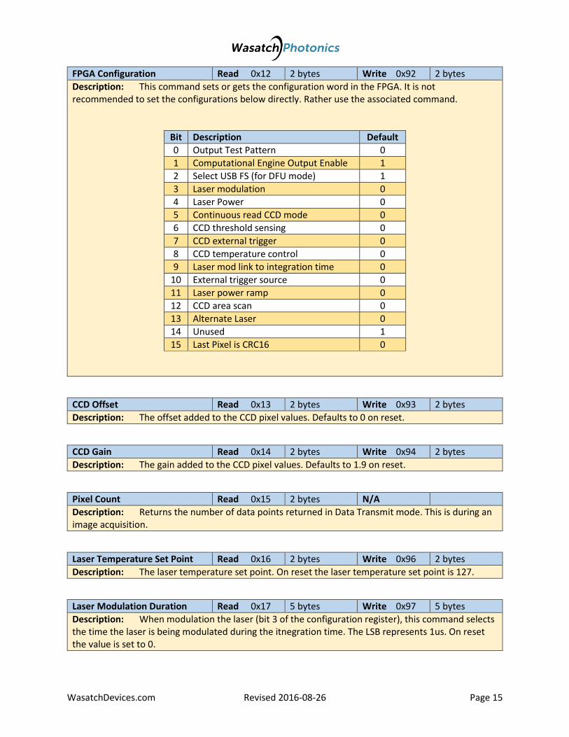
FPGA Configuration Read 0x12 2 bytes Write 0x92 2 bytes
Description: This command sets or gets the configuration word in the FPGA. It is not recommended to set the configurations below directly. Rather use the associated command.
Bit Description Default
0 Output Test Pattern 0
1 Computational Engine Output Enable 1
2 Select USB FS (for DFU mode) 1
3 Laser modulation 0
4 Laser Power 0
5 Continuous read CCD mode 0
6 CCD threshold sensing 0
7 CCD external trigger 0
8 CCD temperature control 0
9 Laser mod link to integration time 0
10 External trigger source 0
11 Laser power ramp 0
12 CCD area scan 0
13 Alternate Laser 0
14 Unused 1
15 Last Pixel is CRC16 0
CCD Offset Read 0x13 2 bytes Write 0x93 2 bytes
Description: The offset added to the CCD pixel values. Defaults to 0 on reset.
CCD Gain Read 0x14 2 bytes Write 0x94 2 bytes
Description: The gain added to the CCD pixel values. Defaults to 1.9 on reset.
Pixel Count Read 0x15 2 bytes N/A
Description: Returns the number of data points returned in Data Transmit mode. This is during an image acquisition.
Laser Temperature Set Point Read 0x16 2 bytes Write 0x96 2 bytes
Description: The laser temperature set point. On reset the laser temperature set point is 127.
Laser Modulation Duration Read 0x17 5 bytes Write 0x97 5 bytes
Description: When modulation the laser (bit 3 of the configuration register), this command selects the time the laser is being modulated during the itnegration time. The LSB represents 1us. On reset the value is set to 0.
WasatchDevices.com Revised 2016-08-26 Page 16
Laser Modulation Pulse Delay Read 0x18 5 bytes Write 0x98 5 bytes
Description: When modulation the laser (bit 3 of the configuration register), this command selects the delay from the start of integration to the beginning of laser modualtion. The LSB represents 1us. On reset the value is set to 0.
Laser Modulation Period Read 0x19 5 bytes Write 0x99 5 bytes
Description: When modulation the laser (bit 3 of the configuration register), this command selects the period of the laser modualtion. The LSB represents 1us. When laser power ramping is enabled, this value determines the length of the ramp. On reset the value is 3162, which corresponds to a 10 second ramp.
Number of Frames to Acquire Read 0x1A 1 byte Write 0x9A 1 byte
Description: This sets the number of frames to acquire with each trigger event. Defaults to 1 on reset.
CCD Data Threshold Read 0x1B 2 bytes Write 0x9B 1 bytes
Description: Sets the threshold for sensing the CCD data. If any value in the CD data frame has a 16-bit value greater than the setpoint, the the POLL_DATA command will return a vlue of 2 rather than 1. Value is an unsigned short. Defaults to 0 on reset.
FPGA Status Read 0x1C 1 byte Write N/A
Description: FPGA Status Register. Current format is TBD.
Laser Temperature Read 0x1D 1 byte Write N/A
Description: Gets the voltage of the thermistor mounted inside or next to the laser. The temperature is represented as a 12-bit value with the top four bits zeroed out. To calculate the temperature from the ADC value, use the code below: Thermistor_Voltage = (ADC_Reading/4096)*2.468; Thermistor_Resistance = Thermistor_Voltage/((2.468-Thermistor_Voltage)/21450)); Temp_in_C = 3977/(log(Thermistor_Resistance/10000) + 3977/(25+273) – 273;
WasatchDevices.com Revised 2016-08-26 Page 17
Laser Modulation Pulse Width Read 0x1E 5 bytes Write 0x9E 5 bytes
Description: When modulating laser (bit 3 of the configuration register), this command selects the pulse width of the laser modulation. The LSB represents 1us. Defaults to 0 on reset.
Actual Integration Time Read 0x1F 3 bytes Write N/A
Description: The command reads the actual integration time. Actual integration time differs from the set integration time under two conditions. 1.) In standard acquistion, the actual integration time will add the clock out time. Therefore, a 1 msec integration time will have an actual integration time of about 4.2 msec. 2.) Under conditions of external triggering, the integration window will be extended to include the output laser pulse time, thus extending the set-point integration time.
Actual Frame Count Read 0x20 2 bytes Write N/A
Description: This command reads the internal frame/capture count. It is incremented for each capture. It is reset to 0 upon power up. Two byte integer value which will roll over after 65,535.
Laser Transition Point 1 - 6 Read 0x21 4 bytes Write 0xA1 4 bytes
Description: Transition points for switching laser. Transition point 1 is command 0x21 and Transition Point 6 is at 0x26.
Laser Transition Point 1 - 6 Read 0x21 4 bytes Write 0xA1 4 bytes
Description: Transition points for switching laser. Transition point 1 is command 0x21 and Transition Point 6 is at 0x26.
Horizontal Binning Read 0x27 1 byte Write 0xA7 1 byte
Description: Enables and disables horizontal binning
Trigger Delay Read 0x28 3 bytes Write 0xA8 3 bytes
Description: The amount of time after an acquisition request to begin acquiring data. The 24-bit register is in units of 0.5 us.
CCD Temperature Read 0x49 2 bytes Write N/A
Description: The ADC value of the thermistor attached to the CDD. This is present in devices with the cooled CCD option. The temperature in centigrade can be calculated in the same manner as the laser temperature on the previous page.
WasatchDevices.com Revised 2016-08-26 Page 18
FPGA Configuration Register Details
Output Test Pattern Read 0x30 1 byte Write 0xA0 1 byte
Description: Data sent out is a pattern instead of real data, starting from 21,864 (0x5556) and counting upward at each data point. No-zero enables and zero disables.
Output Test Pattern Read 0x31 1 byte Write 0xA1 1 byte
Description: Enables custom output specification.
Select FS USB Read 0x32 1 byte Write 0xA2 1 byte
Description: Selects Full Speed USB over High Speed USB. Device must be in Full Speed to update firmware through a DFU process. A non-zero value enables Full Speed. Defaults to High Speed.
Laser Modulation Read 0x33 1 byte Write 0xA3 1 byte
Description: Laser modulation enable. On reset Laser Modulation is disabled.
Laser On Read 0x34 1 byte Write 0xA4 1 byte
Description: Turns Laser ON and OFF. On reset the laser if OFF.
Continuous Read CCD Mode Read 0x35 1 byte Write 0xA5 1 byte
Description: Captures frames continuously after trigger until bit is cleared. Default setting is OFF.
CCD Threshold Sensing Read 0x36 1 byte Write 0xA6 1 byte
Description: The command enables or disables data threshold sensing of the CCD data. When enabled each pixel of the incoming CCD data is compared to a user-defined threshold. If any pixel exceeds the threshold, a bit in the FPGA status register is set. When disabled the status bit is always low. On reset CCD data threshold sensing is disabled.
CCD External Trigger Read 0x37 1 byte Write 0xA7 1 byte
Description: The command enables or disables the laser or, when dealing with an external laser trigger, disables the external trigger signal, setting that value to logic 0 (0 volts). On reset the laser is disabled, so external trigger signaling must be preceded by enabling this line.
CCD Temperature Control Read 0x38 1 byte Write 0xA8 1 byte
Description: The command enables or disables CCD temperature control. When enabled the TEC attached to the CCD will attempt to maintain the CDD at the specified temperature set point. On reset the CCD temperature control is disabled.
WasatchDevices.com Revised 2016-08-26 Page 19
Laser Mod Link to Int. Time Read 0x39 1 byte Write 0xA9 1 byte
Description: The command links the laser modulation (when enabeld) to the integration time.
External Output Trigger Source Read 0x3A 1 byte Write 0xAA 1 byte
Description: Sets trigger source for acquiring data. Defaults to 0 for intenal trigger on reset.
Laser Power Ramp Read 0x3B 1 byte Write 0xAB 1 byte
Description: The command enables or disables ramping of the laser power when the laser is being turned on or off. When laser ramping is enabeld, the Laser Modualtion Period is redefined as the period of the laser ramping. For example, if the laser modualtion period is set to 4, the laser ON signal will be 1-us on, 3-us off; then 2-us off; then 3-us on, 1-us off and then on all the time. On reset laser ramping is disabled.
![TEE Sockets API Specification v1.0 - GlobalPlatform · TEE Sockets API Specification Annex A: TCP/IP Specification of TEE Sockets API Specification [Sockets TCP/IP] GPD_SPE_102 :](https://img.pdfslide.us/doc/110x75/60421070f2b21560856dea9a/tee-sockets-api-specification-v10-globalplatform-tee-sockets-api-specification.jpg)