Embed Size (px)
Citation preview
An Oplink Company
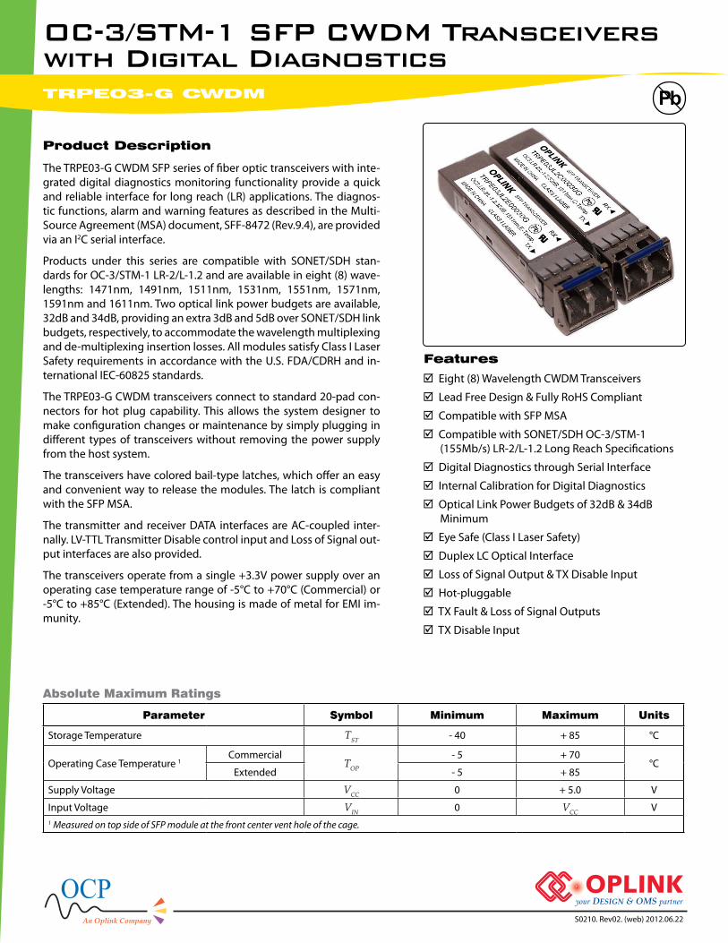
OC-3/STM-1 SFP CWDM Transceivers with Digital DiagnosticsTRPE03-G CWDM
The TRPE03-G CWDM SFP series of fiber optic transceivers with inte-grated digital diagnostics monitoring functionality provide a quick and reliable interface for long reach (LR) applications. The diagnos-tic functions, alarm and warning features as described in the Multi-Source Agreement (MSA) document, SFF-8472 (Rev.9.4), are provided via an I2C serial interface.
Products under this series are compatible with SONET/SDH stan-dards for OC-3/STM-1 LR-2/L-1.2 and are available in eight (8) wave-lengths: 1471nm, 1491nm, 1511nm, 1531nm, 1551nm, 1571nm, 1591nm and 1611nm. Two optical link power budgets are available, 32dB and 34dB, providing an extra 3dB and 5dB over SONET/SDH link budgets, respectively, to accommodate the wavelength multiplexing and de-multiplexing insertion losses. All modules satisfy Class I Laser Safety requirements in accordance with the U.S. FDA/CDRH and in-ternational IEC-60825 standards.
The TRPE03-G CWDM transceivers connect to standard 20-pad con-nectors for hot plug capability. This allows the system designer to make configuration changes or maintenance by simply plugging in different types of transceivers without removing the power supply from the host system.
The transceivers have colored bail-type latches, which offer an easy and convenient way to release the modules. The latch is compliant with the SFP MSA.
The transmitter and receiver DATA interfaces are AC-coupled inter-nally. LV-TTL Transmitter Disable control input and Loss of Signal out-put interfaces are also provided.
The transceivers operate from a single +3.3V power supply over an operating case temperature range of -5°C to +70°C (Commercial) or -5°C to +85°C (Extended). The housing is made of metal for EMI im-munity.
Product Description
Features
S0210. Rev02. (web) 2012.06.22
Absolute Maximum Ratings
Parameter Symbol Minimum Maximum Units
Storage Temperature TST - 40 + 85 °C
Operating Case Temperature 1 Commercial
TOP
- 5 + 70°C
Extended - 5 + 85
Supply Voltage VCC 0 + 5.0 V
Input Voltage VIN 0 VCC V1 Measured on top side of SFP module at the front center vent hole of the cage.
Eight (8) Wavelength CWDM Transceivers
Lead Free Design & Fully RoHS Compliant
Compatible with SFP MSA
Compatible with SONET/SDH OC-3/STM-1 (155Mb/s) LR-2/L-1.2 Long Reach Specifications
Digital Diagnostics through Serial Interface
Internal Calibration for Digital Diagnostics
Optical Link Power Budgets of 32dB & 34dB Minimum
Eye Safe (Class I Laser Safety)
Duplex LC Optical Interface
Loss of Signal Output & TX Disable Input
Hot-pluggable
TX Fault & Loss of Signal Outputs
TX Disable Input
Pb
Oplink Communications, IncS0210. Rev02. (web) 2012.06.222
TRPE03-G CWDM
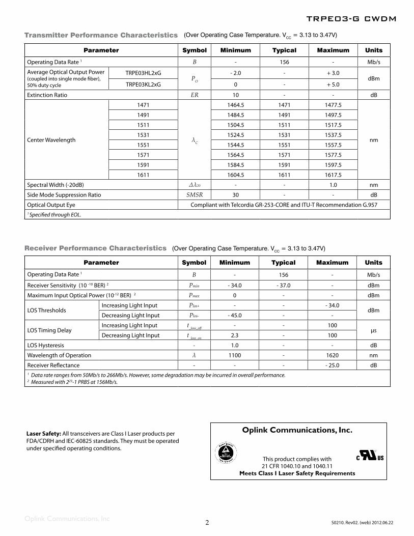
Laser Safety: All transceivers are Class I Laser products per FDA/CDRH and IEC-60825 standards. They must be operated under specified operating conditions.
Oplink Communications, Inc.
This product complies with21 CFR 1040.10 and 1040.11
Meets Class I Laser Safety Requirements
Transmitter Performance Characteristics
Receiver Performance Characteristics (Over Operating Case Temperature. VCC = 3.13 to 3.47V)
Parameter Symbol Minimum Typical Maximum Units
Operating Data Rate 1 B - 156 - Mb/s
Average Optical Output Power (coupled into single mode fiber), 50% duty cycle
TRPE03HL2xGPO
- 2.0 - + 3.0dBm
TRPE03KL2xG 0 - + 5.0
Extinction Ratio ER 10 - - dB
Center Wavelength
1471
λC
1464.5 1471 1477.5
nm
1491 1484.5 1491 1497.5
1511 1504.5 1511 1517.5
1531 1524.5 1531 1537.5
1551 1544.5 1551 1557.5
1571 1564.5 1571 1577.5
1591 1584.5 1591 1597.5
1611 1604.5 1611 1617.5
Spectral Width (-20dB) Δλ20 - - 1.0 nm
Side Mode Suppression Ratio SMSR 30 - - dB
Optical Output Eye Compliant with Telcordia GR-253-CORE and ITU-T Recommendation G.9571 Specified through EOL.
Parameter Symbol Minimum Typical Maximum Units
Operating Data Rate 1 B - 156 - Mb/s
Receiver Sensitivity (10 -10 BER) 2 Pmin - 34.0 - 37.0 - dBm
Maximum Input Optical Power (10-12 BER) 2 Pmax 0 - - dBm
LOS ThresholdsIncreasing Light Input Plos+ - - - 34.0
dBmDecreasing Light Input Plos- - 45.0 - -
LOS Timing DelayIncreasing Light Input t_loss_off - - 100
µsDecreasing Light Input t_loss_on 2.3 - 100
LOS Hysteresis - 1.0 - - dB
Wavelength of Operation λ 1100 - 1620 nm
Receiver Reflectance - - - - 25.0 dB1 Data rate ranges from 50Mb/s to 266Mb/s. However, some degradation may be incurred in overall performance.2 Measured with 223-1 PRBS at 156Mb/s.
(Over Operating Case Temperature. VCC = 3.13 to 3.47V)
Oplink Communications, Inc 3 S0210. Rev02. (web) 2012.06.22
TRPE03-G CWDM
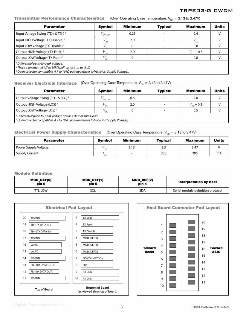
Electrical Pad Layout Host Board Connector Pad Layout
Transmitter Performance Characteristics
TowardBezel
TowardASIC
20
19
18
17
16
15
14
13
12
11
1
2
3
4
5
6
7
8
9
10
20
19
18
17
16
15
14
13
12
11
TX GND
TD- (TX DATA IN-)
TD+ (TX DATA IN+)
TX GND
VccTX
VccRX
RX GND
RD+ (RX DATA OUT+)
RD- (RX DATA OUT-)
RX GND
Top of Board
1
2
3
4
5
6
7
8
9
10
TX GND
TX Fault
TX Disable
MOD_DEF(2)
MOD_DEF(1)
MOD_DEF(0)
NO CONNECTION
LOS
RX GND
RX GND
Bottom of Board(as viewed thru top of board)
(Over Operating Case Temperature. VCC = 3.13 to 3.47V)
Receiver Electrical Interface
Electrical Power Supply Characteristics (Over Operating Case Temperature. VCC = 3.13 to 3.47V)
(Over Operating Case Temperature. VCC = 3.13 to 3.47V)
Module Definition
Parameter Symbol Minimum Typical Maximum Units
Input Voltage Swing (TD+ & TD-) 1 VPP-DIF 0.25 - 2.4 V
Input HIGH Voltage (TX Disable) 2 VIH 2.0 - VCC V
Input LOW Voltage (TX Disable) 2 VIL 0 - 0.8 V
Output HIGH Voltage (TX Fault) 3 VOH 2.0 - VCC + 0.3 V
Output LOW Voltage (TX Fault) 3 VOL 0 - 0.8 V1 Differential peak-to-peak voltage.2 There is an internal 4.7 to 10kΩ pull-up resistor to VccT.3 Open collector compatible, 4.7 to 10kΩ pull-up resistor to Vcc (Host Supply Voltage).
Parameter Symbol Minimum Typical Maximum Units
Power Supply Voltage VCC 3.13 3.3 3.47 V
Supply Current ICC - 235 285 mA
Parameter Symbol Minimum Typical Maximum Units
Output Voltage Swing (RD+ & RD-) 1 VPP-DIF 0.6 - 2.0 V
Output HIGH Voltage (LOS) 2 VOH 2.0 - VCC + 0.3 V
Output LOW Voltage (LOS) 2 VOL 0 - 0.5 V1 Differential peak-to-peak voltage across external 100Ω load.2 Open collector compatible, 4.7 to 10kΩ pull-up resistor to Vcc (Host Supply Voltage).
MOD_DEF(0)pin 6
MOD_DEF(1)pin 5
MOD_DEF(2)pin 4 Interpretation by Host
TTL LOW SCL SDA Serial module definition protocol
Oplink Communications, Inc 4 S0210. Rev02. (web) 2012.06.22
TRPE03-G CWDM
Application Notes
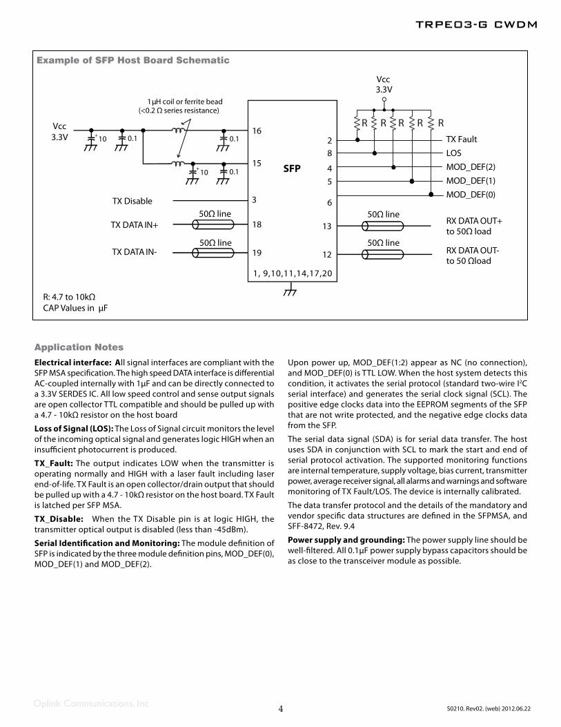
Example of SFP Host Board Schematic
Electrical interface: All signal interfaces are compliant with the SFP MSA specification. The high speed DATA interface is differential AC-coupled internally with 1μF and can be directly connected to a 3.3V SERDES IC. All low speed control and sense output signals are open collector TTL compatible and should be pulled up with a 4.7 - 10kΩ resistor on the host board
Loss of Signal (LOS): The Loss of Signal circuit monitors the level of the incoming optical signal and generates logic HIGH when an insufficient photocurrent is produced.
TX_Fault: The output indicates LOW when the transmitter is operating normally and HIGH with a laser fault including laser end-of-life. TX Fault is an open collector/drain output that should be pulled up with a 4.7 - 10kΩ resistor on the host board. TX Fault is latched per SFP MSA.
TX_Disable: When the TX Disable pin is at logic HIGH, the transmitter optical output is disabled (less than -45dBm).
Serial Identification and Monitoring: The module definition of SFP is indicated by the three module definition pins, MOD_DEF(0), MOD_DEF(1) and MOD_DEF(2).
Upon power up, MOD_DEF(1:2) appear as NC (no connection), and MOD_DEF(0) is TTL LOW. When the host system detects this condition, it activates the serial protocol (standard two-wire I2C serial interface) and generates the serial clock signal (SCL). The positive edge clocks data into the EEPROM segments of the SFP that are not write protected, and the negative edge clocks data from the SFP.
The serial data signal (SDA) is for serial data transfer. The host uses SDA in conjunction with SCL to mark the start and end of serial protocol activation. The supported monitoring functions are internal temperature, supply voltage, bias current, transmitter power, average receiver signal, all alarms and warnings and software monitoring of TX Fault/LOS. The device is internally calibrated.
The data transfer protocol and the details of the mandatory and vendor specific data structures are defined in the SFPMSA, and SFF-8472, Rev. 9.4
Power supply and grounding: The power supply line should be well-filtered. All 0.1μF power supply bypass capacitors should be as close to the transceiver module as possible.
R: 4.7 to 10kΩ CAP Values in μF
TX DATA IN+
1 H coil or ferrite beadµ(<0.2 Ω series resistance)
0.1
TX DATA IN-
TX Disable
0.1+ 10
0.1+ 10
to 50 Ωload
3.3V
RX DATA OUT+
RX DATA OUT-
MOD_DEF(0)
MOD_DEF(1)
MOD_DEF(2)
LOS
to 50Ω load
TX FaultVcc3.3V
Vcc
50Ω line50Ω line
50Ω line 50Ω line
RRRRR
8
54
6
2
18
19
3
15
16
13
12
1, 9,10,11,14,17,20
SFP
4633
5 La
ndin
g Pk
wy
Frem
ont,
CA
945
38 T
el: (
510)
933
-720
0 Fa
x: (5
10) 9
33-7
300
Emai
l: Sal
es@
Opl
ink.
com
• w
ww
.opl
ink.
com
Oplink Communications, Inc. reserves the right to make changes in equipment design or specifications without notice. Information supplied by Oplink Commu-nications, Inc. is believed to be accurate and reliable. However, no responsibility is assumed by Oplink Communications, Inc. for its use nor for any infringements of third parties, which may result from its use. No license is granted by implication or otherwise under any patent right of Oplink Communications, Inc.© 2012, Oplink Communications, Inc.
5 S0210. Rev02. (web) 2012.06.22
TRPE03-G CWDM
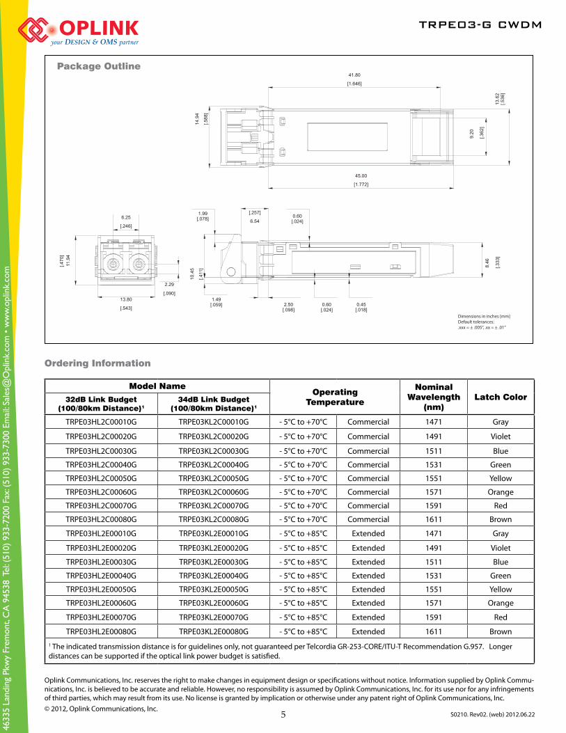
Package Outline
1.49]950.[
1.99]870.[
10.4
5
[.411
]
11.9
4[.4
70]
8.46
[.333
]
0.45]810.[
0.60]420.[
0.60]420.[
13.6
2 [.5
36]
14.9
4
[.588
]
45.00
[1.772]
13.80
[.543]2.50
]890.[
6.54
[.257]
9.20
[.362
]
41.80
[1.646]
6.25
[.246]
2.29
[.090]
Dimensions in inches [mm]Default tolerances:.xxx = ± .005”, .xx = ± .01”
Ordering Information
Model NameOperating
Temperature
Nominal Wavelength
(nm)Latch Color32dB Link Budget
(100/80km Distance)134dB Link Budget
(100/80km Distance)1
TRPE03HL2C00010G TRPE03KL2C00010G - 5°C to +70°C Commercial 1471 Gray
TRPE03HL2C00020G TRPE03KL2C00020G - 5°C to +70°C Commercial 1491 Violet
TRPE03HL2C00030G TRPE03KL2C00030G - 5°C to +70°C Commercial 1511 Blue
TRPE03HL2C00040G TRPE03KL2C00040G - 5°C to +70°C Commercial 1531 Green
TRPE03HL2C00050G TRPE03KL2C00050G - 5°C to +70°C Commercial 1551 Yellow
TRPE03HL2C00060G TRPE03KL2C00060G - 5°C to +70°C Commercial 1571 Orange
TRPE03HL2C00070G TRPE03KL2C00070G - 5°C to +70°C Commercial 1591 Red
TRPE03HL2C00080G TRPE03KL2C00080G - 5°C to +70°C Commercial 1611 Brown
TRPE03HL2E00010G TRPE03KL2E00010G - 5°C to +85°C Extended 1471 Gray
TRPE03HL2E00020G TRPE03KL2E00020G - 5°C to +85°C Extended 1491 Violet
TRPE03HL2E00030G TRPE03KL2E00030G - 5°C to +85°C Extended 1511 Blue
TRPE03HL2E00040G TRPE03KL2E00040G - 5°C to +85°C Extended 1531 Green
TRPE03HL2E00050G TRPE03KL2E00050G - 5°C to +85°C Extended 1551 Yellow
TRPE03HL2E00060G TRPE03KL2E00060G - 5°C to +85°C Extended 1571 Orange
TRPE03HL2E00070G TRPE03KL2E00070G - 5°C to +85°C Extended 1591 Red
TRPE03HL2E00080G TRPE03KL2E00080G - 5°C to +85°C Extended 1611 Brown1 The indicated transmission distance is for guidelines only, not guaranteed per Telcordia GR-253-CORE/ITU-T Recommendation G.957. Longer distances can be supported if the optical link power budget is satisfied.