Embed Size (px)
Citation preview
MPY634
SBFS017A – DECEMBER 1995 – REVISED DECEMBER 2004
www.ti.com
PRODUCTION DATA information is current as of publication date.Products conform to specifications per the terms of Texas Instrumentsstandard warranty. Production processing does not necessarily includetesting of all parameters.
Copyright © 1995-2004, Texas Instruments Incorporated
Please be aware that an important notice concerning availability, standard warranty, and use in critical applications ofTexas Instruments semiconductor products and disclaimers thereto appears at the end of this data sheet.
All trademarks are the property of their respective owners.
FEATURES WIDE BANDWIDTH: 10MHz typ
±0.5% MAX FOUR-QUADRANTACCURACY
INTERNAL WIDE-BANDWIDTH OP AMP
EASY TO USE
LOW COST
APPLICATIONS PRECISION ANALOG SIGNAL
PROCESSING
MODULATION AND DEMODULATION
VOLTAGE-CONTROLLED AMPLIFIERS
VIDEO SIGNAL PROCESSING
VOLTAGE-CONTROLLED FILTERS ANDOSCILLATORS
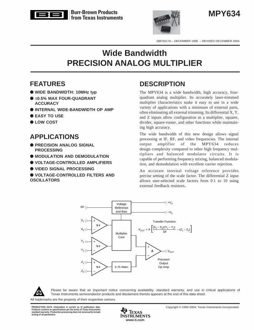
DESCRIPTIONThe MPY634 is a wide bandwidth, high accuracy, four-quadrant analog multiplier. Its accurately laser-trimmedmultiplier characteristics make it easy to use in a widevariety of applications with a minimum of external parts,often eliminating all external trimming. Its differential X, Y,and Z inputs allow configuration as a multiplier, squarer,divider, square-rooter, and other functions while maintain-ing high accuracy.
The wide bandwidth of this new design allows signalprocessing at IF, RF, and video frequencies. The internaloutput amplifier of the MPY634 reducesdesign complexity compared to other high frequency mul-tipliers and balanced modulator circuits. It iscapable of performing frequency mixing, balanced modula-tion, and demodulation with excellent carrier rejection.
An accurate internal voltage reference providesprecise setting of the scale factor. The differential Z inputallows user-selected scale factors from 0.1 to 10 usingexternal feedback resistors.
V-I
X1
X2
Y1
Y2
Z1
Z2
V-I
V-I
SF
MultiplierCore
VoltageReferenceand Bias
0.75 Atten
A VOUT
–VS
+VS
(X1 – X2)(Y1 – Y2)
SFVOUT = A – (Z1 – Z2)
Transfer Function
PrecisionOutput
Op Amp
Wide BandwidthPRECISION ANALOG MULTIPLIER
OB
SO
LE
TE
MPY6342SBFS017Awww.ti.com
SPECIFICATIONSELECTRICALAt T
A = +25°C and V
S = ±15VDC, unless otherwise noted.
MPY634KP/KU MPY634AM MPY634BM MPY634SM
(Z2 – Z1)
(X1 – X2)10V + Y1
(X1 – X
2) (Y
1 – Y
2)
10V+ Z
2
(X1 – X2)2
+ Z210V
(X1 – X2) (Y1 – Y2)
10V+ Z2
(Z2 – Z
1)
(X1 – X
2)
10V + Y1
(X1 – X2)2
+ Z210V
OBSOLETE OBSOLETE OBSOLETEMODEL MIN TYP MAX MIN TYP MAX MIN TYP MAX MIN TYP MAX UNITS
MULTIPLIERPERFORMANCETransfer Function * *Total Error(1)
(–10V ≤ X, Y ≤ +10V) ±2.0 ±1.0 ±0.5 * %TA = min to max ±2.5 ±1.5 ±1.0 ±2.0 %Total Error vs Temperature ±0.03 ±0.022 ±0.015 ±0.02 %/°CScale Factor Error
(SF = 10.000V Nominal)(2) ±0.25 ±0.1 * * %Temperature Coefficient of
Scaling Voltage ±0.02 ±0.01 ±0.01 * %/°CSupply Rejection (±15V ±1V) ±0.01 ±0.01 * * %Nonlinearity
X (X = 20Vp-p, Y = 10V) ±0.4 ±0.4 0.2 ±0.3 * %Y (Y = 20Vp-p, X = 10V) ±0.01 ±0.01 * ±0.1 * %
Feedthrough(3)
X (Y Nulled, X = 20Vp-p, 50Hz) ±0.3 ±0.3 ±0.15 ±0.3 * %Y (X Nulled, Y = 20Vp-p, 50Hz) ±0.01 ±0.01 * ±0.1 * %Both Inputs (500kHz, 1Vrms)
Unnulled 40 50 45 55 * 60 * * dBNulled 55 60 55 65 60 70 * * dB
Output Offset Voltage ±50 ±100 ±5 ±30 * ±15 * * mVOutput Offset Voltage Drift * ±200 ±100 * ±500 µV/°C
DYNAMICSSmall Signal BW,
(VOUT = 0.1Vrms) 6 10 8 10 * * 6 * MHz1% Amplitude Error
(CLOAD = 1000pF) 100 100 * * kHzSlew Rate (VOUT = 20Vp-p) 20 20 * * V/µsSettling Time
(to 1%, ∆VOUT = 20V) 2 2 * * µs
NOISENoise Spectral Density:
SF = 10V 0.8 0.8 * * µV/√HzWideband Noise:
f = 10Hz to 5MHz 1 1 * * mVrmsf = 10Hz to 10kHz 90 90 * * µVrms
OUTPUTOutput Voltage Swing ±11 ±11 * * VOutput Impedance (f ≤ 1kHz) 0.1 0.1 * * ΩOutput Short Circuit Current
(RL = 0, TA = min to max) 30 30 * * mAAmplifier Open Loop Gain
(f = 50Hz) 85 85 * * dB
INPUT AMPLIFIERS (X, Y and Z)Input Voltage Range
Differential VIN (VCM = 0) ±12 ±12 * * VCommon-Mode VIN (VDIFF = 0) ±10 ±10 * * V(see Typical Performance Curves)
Offset Voltage X, Y ±25 ±100 ±5 ±20 ±2 ±10 * * mVOffset Voltage Drift X, Y 200 100 50 * µV/°COffset Voltage Z ±25 ±100 ±5 ±30 ±2 ±15 * * mVOffset Voltage Drift Z 200 200 100 500 µV/°CCMRR 60 80 60 80 70 90 * * dBBias Current 0.8 2.0 0.8 2.0 * * * * µAOffset Current 0.1 0.1 * * 2.0 µADifferential Resistance 10 10 * * MΩ
DIVIDER PERFORMANCETransfer Function (X1 > X2) * *Total Error(1) untrimmed
(X = 10V, –10V ≤ Z ≤ +10V) 1.5 ±0.75 ±0.35 ±0.75 %(X = 1V, –1V ≤ Z ≤ +1V) 4.0 ±2.0 ±1.0 * %(0.1V≤ X ≤ 10V, –10V ≤ Z ≤ 10V) 5.0 ±2.5 ±1.0 * %
SQUARE PERFORMANCETransfer Function * *
Total Error (–10V ≤ X ≤ 10V) ±1.2 ±0.6 ±0.3 * %
MPY634 3SBFS017A www.ti.com
101
5
3
4
X1
–VS
Y2
Y1
SF
X2
2
SOIC: MPY634KUDIP: MPY634KPTO-100: MPY634AM/BM/SM
9
8
7
6Z2
Z1
Out
+VS
1
2
3
4
5
6
7
14
13
12
11
10
9
8
X1 Input
X2 Input
NC
Scale Factor
NC
Y1 Input
Y2 Input
+VS
NC
Output
Z1 Input
Z2 Input
NC
–VS
1
2
3
4
5
6
7
8
16
15
14
13
12
11
10
9
X1 Input
X2 Input
NC
Scale Factor
NC
Y1 Input
Y2 Input
NC
+VS
NC
Output
Z1 Input
Z2 Input
NC
–VS
NC
SPECIFICATIONS (CONT)ELECTRICALAt TA = +25°C and VS = ±15VDC, unless otherwise noted.
MPY634KP/KU MPY634AM MPY634BM MPY634SM
√10V (Z2 – Z1) +X2
* Specification same as for MPY634AM.Gray indicates obsolete parts.NOTES: (1) Figures given are percent of full scale, ±10V (i.e., 0.01% = 1mV). (2) May be reduced to 3V using external resistor between –V
S and SF. (3) Irreducible
component due to nonlinearity; excludes effect of offsets.
PIN CONFIGURATIONS
Basic Model Number
Performance Grade(1)
K: U: –40°C to +85°CPackage Code
P: Plastic 14-pin DIPU: 16-pin SOIC
NOTE: (1) Performance grade identifier may not be marked on the SOICpackage; a blank denotes “K” grade.
ORDERING INFORMATION
MPY634 ( )( )
Top View
PACKAGE DRAWINGPRODUCT PACKAGE NUMBER
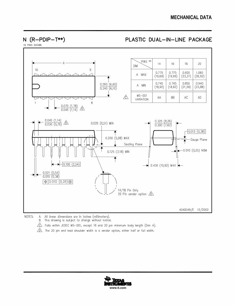
MPY634KP 14-Pin PDIP 010MPY634KU 16-Pin SOIC 211
NOTE: (1) For the most current package and ordering information, see thePackage Option Addendum located at the end of this data sheet.
PACKAGE INFORMATION(1)
√10V (Z2 – Z
1) +X
2
OBSOLETE
OBSOLETE OBSOLETE OBSOLETE
OBSOLETE OBSOLETE
MODEL MIN TYP MAX MIN TYP MAX MIN TYP MAX MIN TYP MAX UNITS
SQUARE-ROOTERPERFORMANCETransfer Function (Z1 ≤ Z2) * *Total Error(1) (1V ≤ Z ≤ 10V) ±2.0 ±1.0 ±0.5 * %
POWER SUPPLYSupply Voltage:
Rated Performance ±15 ±15 * * VDCOperating ±8 ±18 ±8 ±18 * * * ±20 VDC
Supply Current, Quiescent 4 6 4 6 * * * * mA
TEMPERATURE RANGESpecification –40 +85 –25 +85 * * –55 +125 °CStorage –40 +85 –65 +150 * * * * °C
ABSOLUTE MAXIMUM RATINGS
PARAMETER MPY634AM/BM MPY634KP/KU MPY634SM
Power Supply Voltage ±18 * ±20Power Dissipation 500mW * *Output Short-Circuit
to Ground Indefinite * *Input Voltage ( all X,
Y and Z) ±VS * *Temperature Range:
Operating –25°C/+85°C –40°C/+85°C –55°C/+125°CStorage –65°C/+150°C –40°C/+85°C *
Lead Temperature(soldering, 10s) +300°C * *SOIC ‘KU’ Package +260°C
* Specification same as for MPY634AM/BM.NOTE: Gray indicates obsolete parts.
MPY6344SBFS017Awww.ti.com
TYPICAL PERFORMANCE CURVESAt T
A = +25°C, V
S = ±15VDC, unless otherwise noted.
–20
–40
–60
–80
–100
100 1k 10k 1M 10M 100M
Frequency (Hz)
FEEDTHROUGH vs FREQUENCY
Fee
dthr
ough
Atte
nuat
ion
(dB
)
100k
X Feedthrough
Y Feedthrough
10
0
–10
–20
–30
1k 10k 100k 1M 10M 100M
Frequency (Hz)
FREQUENCY RESPONSE AS A MULTIPLIER
Out
put R
espo
nse
(dB
)
CL = 0pF
CL = 1000pFNormal Connection
With X10 FeedbackAttenuator
–50
–60
–70
–80
Temperature (°C)
FEEDTHROUGH vs TEMPERATURE
Fee
dthr
ough
Atte
nuat
ion
(dB
)
–20 20 60 100 140–40 0 40 80 120
fY = 500kHzVX = nulled
nulled at 25°C
–60
90
80
70
60
50
40
30
20
10
0
10k 1M 10M
Frequency (Hz)
COMMON-MODE REJECTION RATIO vs FREQUENCY
CM
RR
(dB
)
100 100M
Typical for all inputs
1.5
1.25
1
0.75
0.5
10 100 10k 100k
Frequency (Hz)
NOISE SPECTRAL DENSITYvs FREQUENCY
Noi
se S
pect
ral D
ensi
ty (
µV/√
Hz)
1k
60
40
20
0
–20
1k 10k 100k 1M 10M 100M
Frequency (Hz)
FREQUENCY RESPONSE AS A DIVIDER
Out
put,
V0/V
2 (d
B)
VX = 100mVDCVZ = 10mVrms
VX = 1VDCVZ = 100mVrms
VX = 10VDCVZ = 100mVrms
MPY634 5SBFS017A www.ti.com
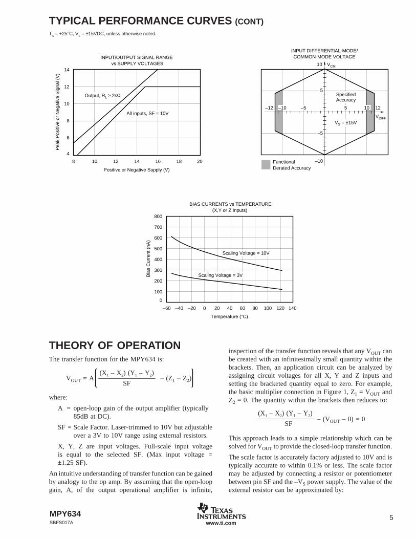
TYPICAL PERFORMANCE CURVES (CONT)T
A = +25°C, V
S = ±15VDC, unless otherwise noted.
THEORY OF OPERATIONThe transfer function for the MPY634 is:
VOUT = A – (Z1 – Z2)
where:
A = open-loop gain of the output amplifier (typically85dB at DC).
SF = Scale Factor. Laser-trimmed to 10V but adjustableover a 3V to 10V range using external resistors.
X, Y, Z are input voltages. Full-scale input voltageis equal to the selected SF. (Max input voltage =±1.25 SF).
An intuitive understanding of transfer function can be gainedby analogy to the op amp. By assuming that the open-loopgain, A, of the output operational amplifier is infinite,
(X1 – X2) (Y1 – Y2)
SF
inspection of the transfer function reveals that any VOUT canbe created with an infinitesimally small quantity within thebrackets. Then, an application circuit can be analyzed byassigning circuit voltages for all X, Y and Z inputs andsetting the bracketed quantity equal to zero. For example,the basic multiplier connection in Figure 1, Z1 = VOUT andZ2 = 0. The quantity within the brackets then reduces to:
– (VOUT – 0) = 0
This approach leads to a simple relationship which can besolved for VOUT to provide the closed-loop transfer function.
The scale factor is accurately factory adjusted to 10V and istypically accurate to within 0.1% or less. The scale factormay be adjusted by connecting a resistor or potentiometerbetween pin SF and the –VS power supply. The value of theexternal resistor can be approximated by:
(X1 – X2) (Y1 – Y2)
SF
14
12
10
8
6
4
8 10 12 16 18 20
Positive or Negative Supply (V)
INPUT/OUTPUT SIGNAL RANGE vs SUPPLY VOLTAGES
Pea
k P
ositi
ve o
r N
egat
ive
Sig
nal (
V)
14
Output, RL ≥ 2kΩ
All inputs, SF = 10V
–10
INPUT DIFFERENTIAL-MODE/COMMON-MODE VOLTAGE
–12 12
10
–5
5
–5 5 10–10
SpecifiedAccuracy
VS = ±15V
FunctionalDerated Accuracy
VCM
VDIFF
800
700
600
500
400
300
200
100
0
–20 0 60 100 140
Temperature (°C)
BIAS CURRENTS vs TEMPERATURE(X,Y or Z Inputs)
Bia
s C
urre
nt (
nA)
20–40 40 80 120
Scaling Voltage = 10V
Scaling Voltage = 3V
–60
MPY6346SBFS017Awww.ti.com
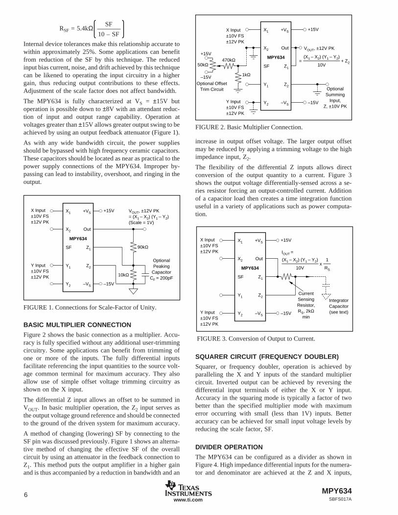
RSF = 5.4kΩ
Internal device tolerances make this relationship accurate towithin approximately 25%. Some applications can benefitfrom reduction of the SF by this technique. The reducedinput bias current, noise, and drift achieved by this techniquecan be likened to operating the input circuitry in a highergain, thus reducing output contributions to these effects.Adjustment of the scale factor does not affect bandwidth.
The MPY634 is fully characterized at VS = ±15V butoperation is possible down to ±8V with an attendant reduc-tion of input and output range capability. Operation atvoltages greater than ±15V allows greater output swing to beachieved by using an output feedback attenuator (Figure 1).
As with any wide bandwidth circuit, the power suppliesshould be bypassed with high frequency ceramic capacitors.These capacitors should be located as near as practical to thepower supply connections of the MPY634. Improper by-passing can lead to instability, overshoot, and ringing in theoutput.
FIGURE 2. Basic Multiplier Connection.
SF
10 – SF
MPY634
X1 +VS
X2 Out
SF Z1
Y1 Z2
Y2 –VS
10kΩ
–15V
+15V
Y Input±10V FS±12V PK
X Input±10V FS±12V PK
90kΩ
VOUT, ±12V PK= (X1 – X2) (Y1 – Y2)(Scale = 1V)
OptionalPeaking
CapacitorCF = 200pF
FIGURE 1. Connections for Scale-Factor of Unity.
BASIC MULTIPLIER CONNECTION
Figure 2 shows the basic connection as a multiplier. Accu-racy is fully specified without any additional user-trimmingcircuitry. Some applications can benefit from trimming ofone or more of the inputs. The fully differential inputsfacilitate referencing the input quantities to the source volt-age common terminal for maximum accuracy. They alsoallow use of simple offset voltage trimming circuitry asshown on the X input.
The differential Z input allows an offset to be summed inVOUT. In basic multiplier operation, the Z2 input serves asthe output voltage ground reference and should be connectedto the ground of the driven system for maximum accuracy.
A method of changing (lowering) SF by connecting to theSF pin was discussed previously. Figure 1 shows an alterna-tive method of changing the effective SF of the overallcircuit by using an attenuator in the feedback connection toZ1. This method puts the output amplifier in a higher gainand is thus accompanied by a reduction in bandwidth and an
increase in output offset voltage. The larger output offsetmay be reduced by applying a trimming voltage to the highimpedance input, Z2.
The flexibility of the differential Z inputs allows directconversion of the output quantity to a current. Figure 3shows the output voltage differentially-sensed across a se-ries resistor forcing an output-controlled current. Additionof a capacitor load then creates a time integration functionuseful in a variety of applications such as power computa-tion.
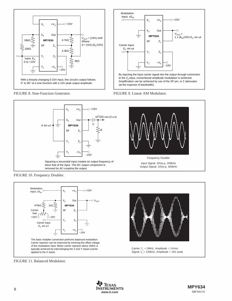
SQUARER CIRCUIT (FREQUENCY DOUBLER)
Squarer, or frequency doubler, operation is achieved byparalleling the X and Y inputs of the standard multipliercircuit. Inverted output can be achieved by reversing thedifferential input terminals of either the X or Y input.Accuracy in the squaring mode is typically a factor of twobetter than the specified multiplier mode with maximumerror occurring with small (less than 1V) inputs. Betteraccuracy can be achieved for small input voltage levels byreducing the scale factor, SF.
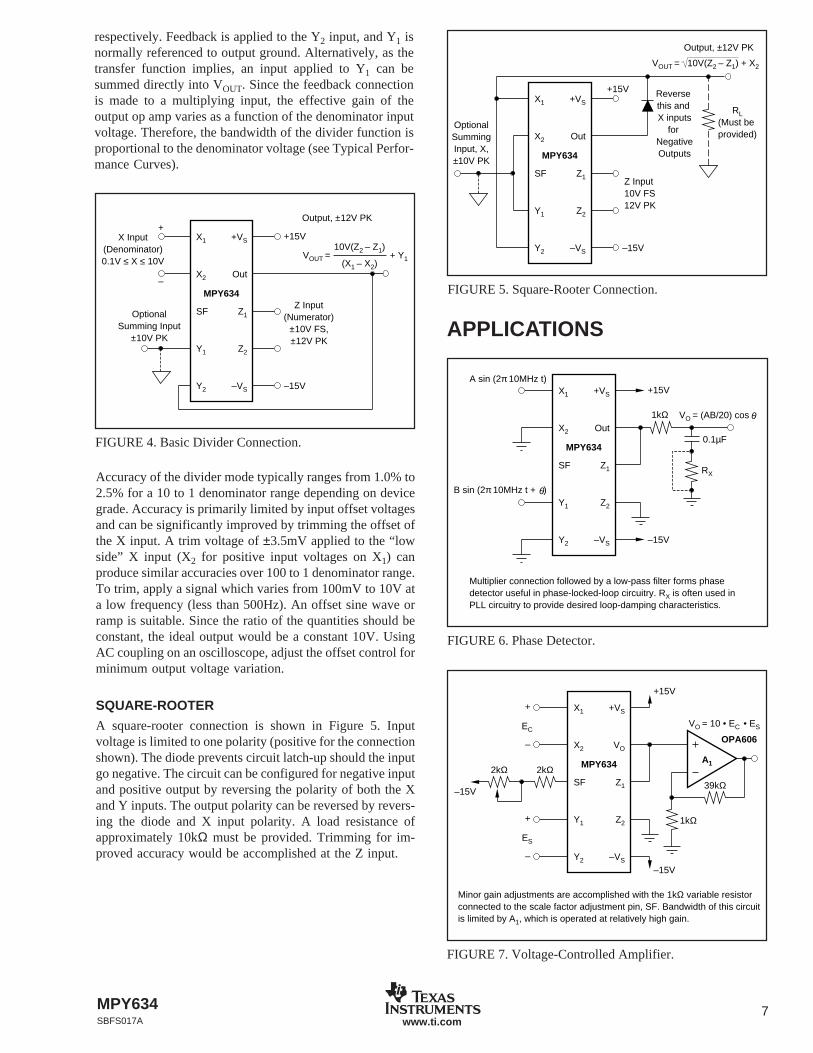
DIVIDER OPERATION
The MPY634 can be configured as a divider as shown inFigure 4. High impedance differential inputs for the numera-tor and denominator are achieved at the Z and X inputs,Hello
FIGURE 3. Conversion of Output to Current.
MPY634
X1 +VS
X2 Out
SF Z1
Y1 Z2
Y2 –VS –15V
+15V
Y Input±10V FS±12V PK
X Input±10V FS±12V PK
CurrentSensingResistor,RS, 2kΩ
min
IntegratorCapacitor(see text)
IOUT =
x (X1 – X2) (Y1 – Y2)
10V
1
RS
MPY634
X1 +VS
X2 Out
SF Z1
Y1 Z2
Y2 –VS –15V
+15V
Y Input±10V FS±12V PK
X Input±10V FS±12V PK
470kΩ
OptionalSumming
Input,Z, ±10V PK
+ Z2 (X1 – X2) (Y1 – Y2)
10V50kΩ
+15V
–15V 1kΩ
Optional OffsetTrim Circuit
VOUT, ±12V PK
=
MPY634 7SBFS017A www.ti.com
respectively. Feedback is applied to the Y2 input, and Y1 isnormally referenced to output ground. Alternatively, as thetransfer function implies, an input applied to Y1 can besummed directly into VOUT. Since the feedback connectionis made to a multiplying input, the effective gain of theoutput op amp varies as a function of the denominator inputvoltage. Therefore, the bandwidth of the divider function isproportional to the denominator voltage (see Typical Perfor-mance Curves).
FIGURE 5. Square-Rooter Connection.
APPLICATIONS
FIGURE 6. Phase Detector.
FIGURE 7. Voltage-Controlled Amplifier.
MPY634
X1 +VS
X2 Out
SF Z1
Y1 Z2
Y2 –VS –15V
+15V
VO = (AB/20) cos
0.1µF
RX
A sin (2π 10MHz t)
B sin (2π 10MHz t + )
Multiplier connection followed by a low-pass filter forms phasedetector useful in phase-locked-loop circuitry. RX is often used in PLL circuitry to provide desired loop-damping characteristics.
1kΩ θ
θ
MPY634
X1 +VS
X2 Out
SF Z1
Y1 Z2
Y2 –VS –15V
+15V
Z Input10V FS12V PK
VOUT = 10V(Z2 – Z1) + X2
Output, ±12V PK
RL(Must be provided)
Reverse this and X inputs
for NegativeOutputs
OptionalSummingInput, X,±10V PK
FIGURE 4. Basic Divider Connection.
Accuracy of the divider mode typically ranges from 1.0% to2.5% for a 10 to 1 denominator range depending on devicegrade. Accuracy is primarily limited by input offset voltagesand can be significantly improved by trimming the offset ofthe X input. A trim voltage of ±3.5mV applied to the “lowside” X input (X2 for positive input voltages on X1) canproduce similar accuracies over 100 to 1 denominator range.To trim, apply a signal which varies from 100mV to 10V ata low frequency (less than 500Hz). An offset sine wave orramp is suitable. Since the ratio of the quantities should beconstant, the ideal output would be a constant 10V. UsingAC coupling on an oscilloscope, adjust the offset control forminimum output voltage variation.
SQUARE-ROOTER
A square-rooter connection is shown in Figure 5. Inputvoltage is limited to one polarity (positive for the connectionshown). The diode prevents circuit latch-up should the inputgo negative. The circuit can be configured for negative inputand positive output by reversing the polarity of both the Xand Y inputs. The output polarity can be reversed by revers-ing the diode and X input polarity. A load resistance ofapproximately 10kΩ must be provided. Trimming for im-proved accuracy would be accomplished at the Z input.
MPY634
X1 +VS
X2 VO
SF Z1
Y1 Z2
Y2 –VS
–15V
+15V
OPA606
1kΩ
Minor gain adjustments are accomplished with the 1kΩ variable resistor connected to the scale factor adjustment pin, SF. Bandwidth of this circuit is limited by A1, which is operated at relatively high gain.
A1
39kΩ
2kΩ 2kΩ
+
–
ES
+
–
EC
–15V
VO = 10 • EC • ES
MPY634
X1 +VS
X2 Out
SF Z1
Y1 Z2
Y2 –VS –15V
+15V
OptionalSumming Input
±10V PK
X Input(Denominator)0.1V ≤ X ≤ 10V
Z Input(Numerator)
±10V FS,±12V PK
+
–
(X1 – X2)VOUT = + Y1
10V(Z2 – Z1)
Output, ±12V PK
MPY6348SBFS017Awww.ti.com
FIGURE 9. Linear AM Modulator.FIGURE 8. Sine-Function Generator.
MPY634
X1 +VS
X2 Out
SF Z1
Y1 Z2
Y2 –VS–15V
+15V
VOUT = (10V) sinWhere = (π/2) (E /10V)
4.7kΩ
Input, E 0 to +10V
With a linearly changing 0-10V input, this circuit’s output follows 0° to 90° of a sine function with a 10V peak output amplitude.
4.3kΩ
3kΩ
10kΩ
18kΩ
θ
θ θ
θ
FIGURE 11. Balanced Modulator.
Carrier: fC = 2MHz, Amplitude = 1VrmsSignal: fS = 120kHz, Amplitude = 10V peak
MPY634
X1 +VS
X2 Out
SF Z1
Y1 Z2
Y2 –VS–15V
+15V
Carrier InputEC sin ω t
The basic muliplier connection performs balanced modulation.Carrier rejection can be improved by trimming the offset voltageof the modulation input. Better carrier rejection above 2MHz is typically achieved by interchanging the X and Y inputs (carrierapplied to the X input).
1kΩ
VOUT
470kΩ
+15V –15V
Modulation Input, ±EM
CarrierNull
FIGURE 10. Frequency Doubler.
Frequency Doubler
Input Signal: 20Vp-p, 200kHzOutput Signal: 10Vp-p, 400kHz
MPY634
X1 +VS
X2 Out
SF Z1
Y1 Z2
Y2 –VS
(A2/20) cos (2 ω t)
Squaring a sinusoidal input creates an output frequency of twice that of the input. The DC output component is removed by AC-coupling the output.
R
CA sin ω t
–15V
+15V
MPY634
X1 +VS
X2 Out
SF Z1
Y1 Z2
Y2 –VS–15V
+15V
VOUT = 1 ± (EM/10V) EC sin ωt
Carrier InputEC sin ωt
By injecting the input carrier signal into the output through connection to the Z2 input, conventional amplitude modulation is achieved. Amplification can be achieved by use of the SF pin, or Z attenuator (at the expense of bandwidth).
ModulationInput, ±EM
PACKAGE OPTION ADDENDUM
www.ti.com 17-Mar-2017
Addendum-Page 1
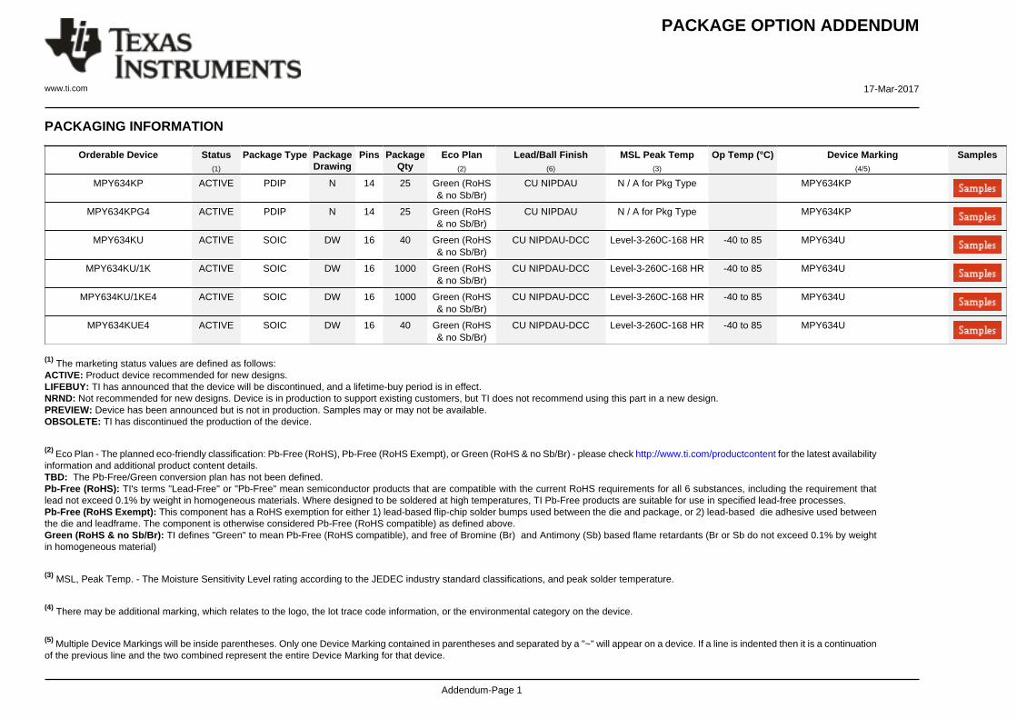
PACKAGING INFORMATION
Orderable Device Status(1)
Package Type PackageDrawing
Pins PackageQty
Eco Plan(2)
Lead/Ball Finish(6)
MSL Peak Temp(3)
Op Temp (°C) Device Marking(4/5)
Samples
MPY634KP ACTIVE PDIP N 14 25 Green (RoHS& no Sb/Br)
CU NIPDAU N / A for Pkg Type MPY634KP
MPY634KPG4 ACTIVE PDIP N 14 25 Green (RoHS& no Sb/Br)
CU NIPDAU N / A for Pkg Type MPY634KP
MPY634KU ACTIVE SOIC DW 16 40 Green (RoHS& no Sb/Br)
CU NIPDAU-DCC Level-3-260C-168 HR -40 to 85 MPY634U
MPY634KU/1K ACTIVE SOIC DW 16 1000 Green (RoHS& no Sb/Br)
CU NIPDAU-DCC Level-3-260C-168 HR -40 to 85 MPY634U
MPY634KU/1KE4 ACTIVE SOIC DW 16 1000 Green (RoHS& no Sb/Br)
CU NIPDAU-DCC Level-3-260C-168 HR -40 to 85 MPY634U
MPY634KUE4 ACTIVE SOIC DW 16 40 Green (RoHS& no Sb/Br)
CU NIPDAU-DCC Level-3-260C-168 HR -40 to 85 MPY634U
(1) The marketing status values are defined as follows:ACTIVE: Product device recommended for new designs.LIFEBUY: TI has announced that the device will be discontinued, and a lifetime-buy period is in effect.NRND: Not recommended for new designs. Device is in production to support existing customers, but TI does not recommend using this part in a new design.PREVIEW: Device has been announced but is not in production. Samples may or may not be available.OBSOLETE: TI has discontinued the production of the device.
(2) Eco Plan - The planned eco-friendly classification: Pb-Free (RoHS), Pb-Free (RoHS Exempt), or Green (RoHS & no Sb/Br) - please check http://www.ti.com/productcontent for the latest availabilityinformation and additional product content details.TBD: The Pb-Free/Green conversion plan has not been defined.Pb-Free (RoHS): TI's terms "Lead-Free" or "Pb-Free" mean semiconductor products that are compatible with the current RoHS requirements for all 6 substances, including the requirement thatlead not exceed 0.1% by weight in homogeneous materials. Where designed to be soldered at high temperatures, TI Pb-Free products are suitable for use in specified lead-free processes.Pb-Free (RoHS Exempt): This component has a RoHS exemption for either 1) lead-based flip-chip solder bumps used between the die and package, or 2) lead-based die adhesive used betweenthe die and leadframe. The component is otherwise considered Pb-Free (RoHS compatible) as defined above.Green (RoHS & no Sb/Br): TI defines "Green" to mean Pb-Free (RoHS compatible), and free of Bromine (Br) and Antimony (Sb) based flame retardants (Br or Sb do not exceed 0.1% by weightin homogeneous material)
(3) MSL, Peak Temp. - The Moisture Sensitivity Level rating according to the JEDEC industry standard classifications, and peak solder temperature.
(4) There may be additional marking, which relates to the logo, the lot trace code information, or the environmental category on the device.
(5) Multiple Device Markings will be inside parentheses. Only one Device Marking contained in parentheses and separated by a "~" will appear on a device. If a line is indented then it is a continuationof the previous line and the two combined represent the entire Device Marking for that device.
PACKAGE OPTION ADDENDUM
www.ti.com 17-Mar-2017
Addendum-Page 2
(6) Lead/Ball Finish - Orderable Devices may have multiple material finish options. Finish options are separated by a vertical ruled line. Lead/Ball Finish values may wrap to two lines if the finishvalue exceeds the maximum column width.
Important Information and Disclaimer:The information provided on this page represents TI's knowledge and belief as of the date that it is provided. TI bases its knowledge and belief on informationprovided by third parties, and makes no representation or warranty as to the accuracy of such information. Efforts are underway to better integrate information from third parties. TI has taken andcontinues to take reasonable steps to provide representative and accurate information but may not have conducted destructive testing or chemical analysis on incoming materials and chemicals.TI and TI suppliers consider certain information to be proprietary, and thus CAS numbers and other limited information may not be available for release.
In no event shall TI's liability arising out of such information exceed the total purchase price of the TI part(s) at issue in this document sold by TI to Customer on an annual basis.
TAPE AND REEL INFORMATION
*All dimensions are nominal
Device PackageType
PackageDrawing
Pins SPQ ReelDiameter
(mm)
ReelWidth
W1 (mm)
A0(mm)
B0(mm)
K0(mm)
P1(mm)
W(mm)
Pin1Quadrant
MPY634KU/1K SOIC DW 16 1000 330.0 16.4 10.75 10.7 2.7 12.0 16.0 Q1
PACKAGE MATERIALS INFORMATION
www.ti.com 9-Sep-2016
Pack Materials-Page 1
*All dimensions are nominal
Device Package Type Package Drawing Pins SPQ Length (mm) Width (mm) Height (mm)
MPY634KU/1K SOIC DW 16 1000 367.0 367.0 38.0
PACKAGE MATERIALS INFORMATION
www.ti.com 9-Sep-2016
Pack Materials-Page 2
GENERIC PACKAGE VIEW
Images above are just a representation of the package family, actual package may vary.Refer to the product data sheet for package details.
DW 16 SOIC - 2.65 mm max heightSMALL OUTLINE INTEGRATED CIRCUIT
4040000-2/H
www.ti.com
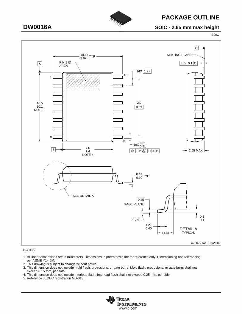
PACKAGE OUTLINE
C
TYP10.639.97
2.65 MAX
14X 1.27
16X 0.510.31
2X8.89
TYP0.330.10
0 - 80.30.1
(1.4)
0.25GAGE PLANE
1.270.40
A
NOTE 3
10.510.1
BNOTE 4
7.67.4
4220721/A 07/2016
SOIC - 2.65 mm max heightDW0016ASOIC
NOTES: 1. All linear dimensions are in millimeters. Dimensions in parenthesis are for reference only. Dimensioning and tolerancing per ASME Y14.5M. 2. This drawing is subject to change without notice. 3. This dimension does not include mold flash, protrusions, or gate burrs. Mold flash, protrusions, or gate burrs shall not exceed 0.15 mm, per side. 4. This dimension does not include interlead flash. Interlead flash shall not exceed 0.25 mm, per side.5. Reference JEDEC registration MS-013.
1 16
0.25 C A B
98
PIN 1 IDAREA
SEATING PLANE
0.1 C
SEE DETAIL A
DETAIL ATYPICAL
SCALE 1.500
www.ti.com
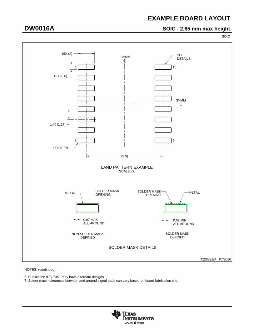
EXAMPLE BOARD LAYOUT
0.07 MAXALL AROUND
0.07 MINALL AROUND
(9.3)
14X (1.27)
R0.05 TYP
16X (2)
16X (0.6)
4220721/A 07/2016
SOIC - 2.65 mm max heightDW0016ASOIC
NOTES: (continued) 6. Publication IPC-7351 may have alternate designs. 7. Solder mask tolerances between and around signal pads can vary based on board fabrication site.
METAL SOLDER MASKOPENING
NON SOLDER MASKDEFINED
SOLDER MASK DETAILS
OPENINGSOLDER MASK METAL
SOLDER MASKDEFINED
LAND PATTERN EXAMPLESCALE:7X
SYMM
1
8 9
16
SEEDETAILS
SYMM
www.ti.com
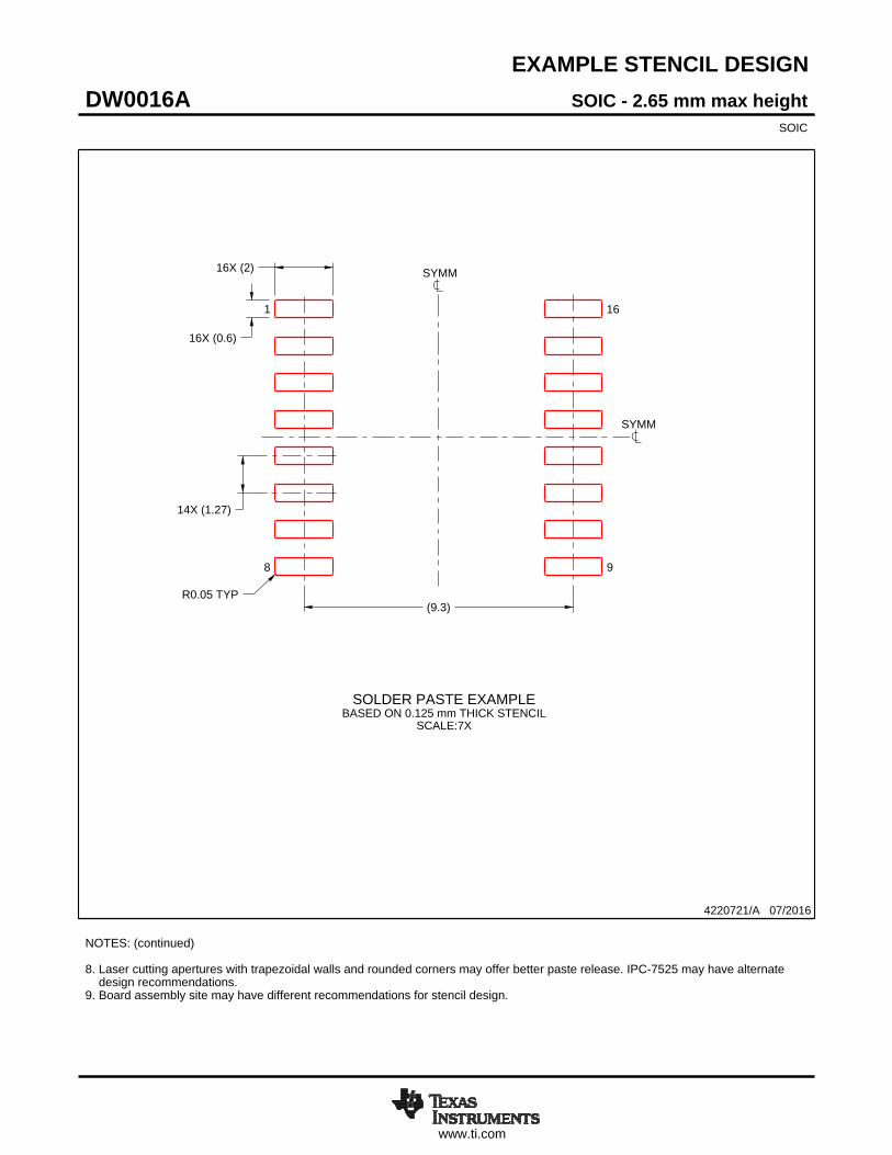
EXAMPLE STENCIL DESIGN
R0.05 TYP
16X (2)
16X (0.6)
14X (1.27)
(9.3)
4220721/A 07/2016
SOIC - 2.65 mm max heightDW0016ASOIC
NOTES: (continued) 8. Laser cutting apertures with trapezoidal walls and rounded corners may offer better paste release. IPC-7525 may have alternate design recommendations. 9. Board assembly site may have different recommendations for stencil design.
SOLDER PASTE EXAMPLEBASED ON 0.125 mm THICK STENCIL
SCALE:7X
SYMM
SYMM
1
8 9
16
IMPORTANT NOTICE
Texas Instruments Incorporated (TI) reserves the right to make corrections, enhancements, improvements and other changes to itssemiconductor products and services per JESD46, latest issue, and to discontinue any product or service per JESD48, latest issue. Buyersshould obtain the latest relevant information before placing orders and should verify that such information is current and complete.TI’s published terms of sale for semiconductor products (http://www.ti.com/sc/docs/stdterms.htm) apply to the sale of packaged integratedcircuit products that TI has qualified and released to market. Additional terms may apply to the use or sale of other types of TI products andservices.Reproduction of significant portions of TI information in TI data sheets is permissible only if reproduction is without alteration and isaccompanied by all associated warranties, conditions, limitations, and notices. TI is not responsible or liable for such reproduceddocumentation. Information of third parties may be subject to additional restrictions. Resale of TI products or services with statementsdifferent from or beyond the parameters stated by TI for that product or service voids all express and any implied warranties for theassociated TI product or service and is an unfair and deceptive business practice. TI is not responsible or liable for any such statements.Buyers and others who are developing systems that incorporate TI products (collectively, “Designers”) understand and agree that Designersremain responsible for using their independent analysis, evaluation and judgment in designing their applications and that Designers havefull and exclusive responsibility to assure the safety of Designers' applications and compliance of their applications (and of all TI productsused in or for Designers’ applications) with all applicable regulations, laws and other applicable requirements. Designer represents that, withrespect to their applications, Designer has all the necessary expertise to create and implement safeguards that (1) anticipate dangerousconsequences of failures, (2) monitor failures and their consequences, and (3) lessen the likelihood of failures that might cause harm andtake appropriate actions. Designer agrees that prior to using or distributing any applications that include TI products, Designer willthoroughly test such applications and the functionality of such TI products as used in such applications.TI’s provision of technical, application or other design advice, quality characterization, reliability data or other services or information,including, but not limited to, reference designs and materials relating to evaluation modules, (collectively, “TI Resources”) are intended toassist designers who are developing applications that incorporate TI products; by downloading, accessing or using TI Resources in anyway, Designer (individually or, if Designer is acting on behalf of a company, Designer’s company) agrees to use any particular TI Resourcesolely for this purpose and subject to the terms of this Notice.TI’s provision of TI Resources does not expand or otherwise alter TI’s applicable published warranties or warranty disclaimers for TIproducts, and no additional obligations or liabilities arise from TI providing such TI Resources. TI reserves the right to make corrections,enhancements, improvements and other changes to its TI Resources. TI has not conducted any testing other than that specificallydescribed in the published documentation for a particular TI Resource.Designer is authorized to use, copy and modify any individual TI Resource only in connection with the development of applications thatinclude the TI product(s) identified in such TI Resource. NO OTHER LICENSE, EXPRESS OR IMPLIED, BY ESTOPPEL OR OTHERWISETO ANY OTHER TI INTELLECTUAL PROPERTY RIGHT, AND NO LICENSE TO ANY TECHNOLOGY OR INTELLECTUAL PROPERTYRIGHT OF TI OR ANY THIRD PARTY IS GRANTED HEREIN, including but not limited to any patent right, copyright, mask work right, orother intellectual property right relating to any combination, machine, or process in which TI products or services are used. Informationregarding or referencing third-party products or services does not constitute a license to use such products or services, or a warranty orendorsement thereof. Use of TI Resources may require a license from a third party under the patents or other intellectual property of thethird party, or a license from TI under the patents or other intellectual property of TI.TI RESOURCES ARE PROVIDED “AS IS” AND WITH ALL FAULTS. TI DISCLAIMS ALL OTHER WARRANTIES ORREPRESENTATIONS, EXPRESS OR IMPLIED, REGARDING RESOURCES OR USE THEREOF, INCLUDING BUT NOT LIMITED TOACCURACY OR COMPLETENESS, TITLE, ANY EPIDEMIC FAILURE WARRANTY AND ANY IMPLIED WARRANTIES OFMERCHANTABILITY, FITNESS FOR A PARTICULAR PURPOSE, AND NON-INFRINGEMENT OF ANY THIRD PARTY INTELLECTUALPROPERTY RIGHTS. TI SHALL NOT BE LIABLE FOR AND SHALL NOT DEFEND OR INDEMNIFY DESIGNER AGAINST ANY CLAIM,INCLUDING BUT NOT LIMITED TO ANY INFRINGEMENT CLAIM THAT RELATES TO OR IS BASED ON ANY COMBINATION OFPRODUCTS EVEN IF DESCRIBED IN TI RESOURCES OR OTHERWISE. IN NO EVENT SHALL TI BE LIABLE FOR ANY ACTUAL,DIRECT, SPECIAL, COLLATERAL, INDIRECT, PUNITIVE, INCIDENTAL, CONSEQUENTIAL OR EXEMPLARY DAMAGES INCONNECTION WITH OR ARISING OUT OF TI RESOURCES OR USE THEREOF, AND REGARDLESS OF WHETHER TI HAS BEENADVISED OF THE POSSIBILITY OF SUCH DAMAGES.Unless TI has explicitly designated an individual product as meeting the requirements of a particular industry standard (e.g., ISO/TS 16949and ISO 26262), TI is not responsible for any failure to meet such industry standard requirements.Where TI specifically promotes products as facilitating functional safety or as compliant with industry functional safety standards, suchproducts are intended to help enable customers to design and create their own applications that meet applicable functional safety standardsand requirements. Using products in an application does not by itself establish any safety features in the application. Designers mustensure compliance with safety-related requirements and standards applicable to their applications. Designer may not use any TI products inlife-critical medical equipment unless authorized officers of the parties have executed a special contract specifically governing such use.Life-critical medical equipment is medical equipment where failure of such equipment would cause serious bodily injury or death (e.g., lifesupport, pacemakers, defibrillators, heart pumps, neurostimulators, and implantables). Such equipment includes, without limitation, allmedical devices identified by the U.S. Food and Drug Administration as Class III devices and equivalent classifications outside the U.S.TI may expressly designate certain products as completing a particular qualification (e.g., Q100, Military Grade, or Enhanced Product).Designers agree that it has the necessary expertise to select the product with the appropriate qualification designation for their applicationsand that proper product selection is at Designers’ own risk. Designers are solely responsible for compliance with all legal and regulatoryrequirements in connection with such selection.Designer will fully indemnify TI and its representatives against any damages, costs, losses, and/or liabilities arising out of Designer’s non-compliance with the terms and provisions of this Notice.
Mailing Address: Texas Instruments, Post Office Box 655303, Dallas, Texas 75265Copyright © 2017, Texas Instruments Incorporated