Embed Size (px)
Citation preview
I
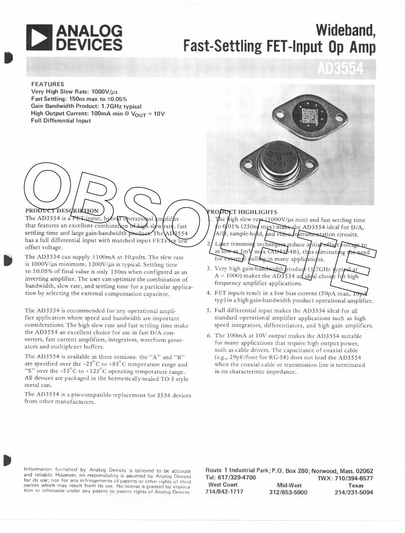
-.. ANALOGW DEVICES
FEATURES
Very High Slew Rate: 1000V/I1SFast Settling: 150ns max to to.05%Gain Bandwidth Product: 1.7GHz typicalHigh Output Current: 100mA min @ VOUT = 10VFull Differential Input
I
PRODUCT DESCRIPTION
The AD3554 is a FET-input, hybrid operational amplifierthat features an excellent combination of high slew rate, fastsettling time and large gain-bandwidth product. The AD3554has a full differential input with matched inpu t FETs for lowoffset voltage.
The AD3554 can supply t100mA at 10..\lolts. The slew rateis 1000VII1s minimum; 1200VII1s is typical. Settling timeto to.05% of final value is only 150ns when configured as aninverting amplifier. The user can optimize the combination ofbandwidth, slew rate, and settling time for a particular applica-tion by selecting the external compensation capacitor.
The AD 3554 is recommended for any operational ampli-fier application where speed and bandwidth are importantconsiderations. The high slew rate and fast settling time makethe AD3 554 an excellent choice for use in fast DIA con-verters, fast current amplifiers, integrators, waveform gener-ators and multiplexer buffers.
The AD3554 is available in three versions: the "A" and "B"
are specified over the -25°C to +85°C temperature range and"S" over the -55°C to +125°C operating temperature range.All devices are packaged in the hermetically-sealed TO-3 stylemetal can.
The AD3554 is a pin-compatible replacement for 3554 devicesfrom other manufacturers.
-Information furnished by Analog Devices is believed to be accurateand reliable. However, no responsibility is assumed by Analog Devicesfor its use; nor for any infringements of patents or other rights of thirdparties which may result from its use. No license is granted by implica-tion or otherwise under any patent or patent rights of Analog Devices.
Wideband,Fast-SettlingFET-InputOpAmp
PRODUCT HIGHLIGHTS
1. The high slew rate (lOOOVll1smin) and fast settling timeto 0.01% (25 Ons max) make the AD 3554 ideal for DIA,AID, sample-hold, and video instrumentation circuits.
2. Laser trimming techniques reduce initial offset voltage toas low as 1mV max (AD3554B), thus eliminating the needfor external nulling in many applications.
3. Very high gain-bandwidth product (1.7GHz typical atA = 1000) makes the AD3554 an ideal choice for highfrequency amplifier applications.
4. FET inputs result in a low bias current (50pA max, lOpAtyp) in a high gain-bandwidth product operational amplifier.
5. Full differential input makes the AD3554 ideal for allstandard operational amplifier applications such as highspeed integrators, differentiators, and high gain amplifiers.
6. The 100mA at 10V output makes the AD3554 suitablefor many applications that require high output power,such as cable drivers. The capacitance of coaxial cable(e.g., 29pF/foot for RG-58) does not load the AD3554when the coaxial cable or transmission line is terminatedin its characteristic impedance.
Route 1 Industrial Park; P.O. Box 280; Norwood, Mass. 02062Tel: 617/329-4700 1WX: 710/394-6577West Coast Mid-West Texas
714/842-1717 312/653-5000 214/231-5094
-- ---
OBSOLETE
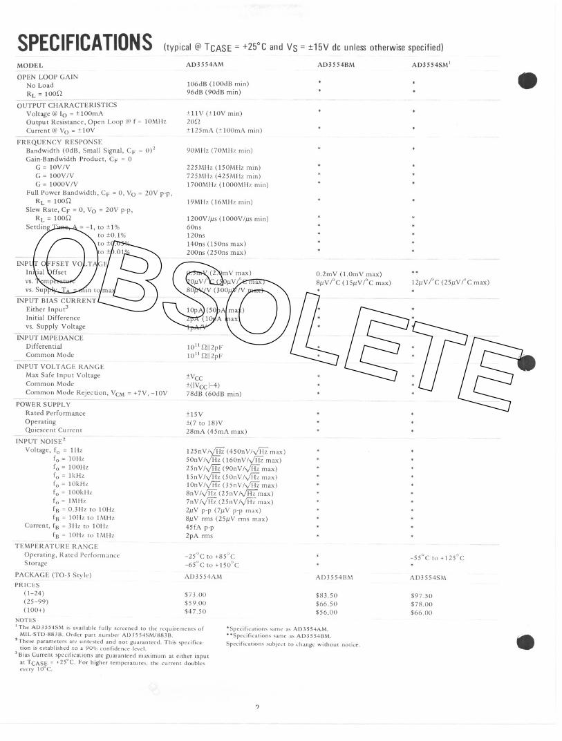
SPECIFICATIONS (typical @ TCASE = +25°C and Vs = :t15V dc unless otherwise specified)
AD3554SM!MODEL
OPEN LOOP GAINNo Load
RL = lOOn
OUTPUT CHARACTERISTICS
Voltage@ 10 = :tIOOmAOu tpu t Resistance, Open Loop @ f =Current @ Vo = :':IOV
FREQUENCY RESPONSEBandwidth (OdB, Small Signal, CF = 0)2Gain-Bandwidth Product, CF = 0
G = lOVIVG = 1O0VIVG = 1000VIV
Full Power Bandwidth, CF = 0, Vo = 20V p-p,RL = lOOn
Slew Rate, CF = 0, Vo = 20V p-p,RL = lOOn
Settling Time, A = -1, to :':1%to :':0.1%to :':0.05%to:':O.Ol%
10MHz
INPUT OFFSET VOLTAGEInitial Offset
vs. Temperature
vs. Supply, TA = min to max
INP UT~BTASCURRENT
Either Input3Initial Difference
vs. Supply Voltage
INPUT-iMPEDANCE'DifferentialCommon Mode
INPUT VOLTAGE RANGE
Max Safe Input VoltageCommon Mode
Common Mode Rejection, VCM = +7V, -10V
POWER SUPPLYRated Performance
OperatingQuiescent Current
INPUT NOISE2
Voltage, fo = 1Hzfa = 10Hzfa = 100Hzfa = 1kHzfa = 10kHzfa = 100kHzfa = 1MHzfB = 0.3Hz to 10HzfB = 10Hz to 1MHz
Current, fB = 3Hz to 10Hz
fB = 10Hz to 1MHz
TEMPERATURE RANGE
Operating, Rated PerformanceStorage
PACKAGE (TO.3 Style)PRICES
(1-24)(25-99)(100+ )
AD3554AM
106dB (lOOdB min)96dB (90dB min)
:':llV (:tIOV min)20n
:':125mA (:tIOOmA min)
90MHz (70MHz min)
225MHz (l50MHz min)72SMHz (42SMHz min)1700MHz (lOOOMHz min)
19MHz (l6MHz min)
1200VI/ls (lOOOVI/ls min)60ns120ns
140ns (lSOns max)2oons (2S0ns max)
0.5mV (2.0mV max)
20/lV/C (50/lV/oC max)80/lVIV (300/lVN max)
lOpA (50pA max)2pA (lOpA max)1pAN
1011 nll2pFloll nll2pF
:':VCC:':( IV cc 1-4 )
78dB (60dB min)
:':15V
:':(7 to 18)V28mA (45mA max)
12SnV/VHz (4S0nV/yHz max)50nV IVHz (l60nV IVHz max)2SnV/VHz (90nV/VHz max)15nV/VHz (SOnV/VHz max)10nV/YHz (3SnV/YfiZ max)8nV/.JHZ (2SnV/v'Hz max)7nV/VHz (2SnV/yHz max)
2/lV p'p (7/lV pop max)8/lV rIDS (25/lV rms max)
4SfA pop2pA rIDS
-2S0C to +8SoC-6SoC to +lS0°C
AD3S54AM
$73.00$59.00$47.50
NOTES
'The AD3554SM is available fully screened to the requirements ofMIL-STD-883B. Order part number AD3554SM/883B.
'These parameters are untested and not guaranteed. This specifica-tion is established to a 90% confidence level.
'Bias Current specifications are guaranteed maximum at either inputat TCASE = +25°C. For higher temperatures, the current doublesevery WOC.
AD3554BM
0.2mV (l.OmV max)8/lV/C (l5/lV/C max)
AD3554BM
$83.50$66.50$56.00
'Specifications same as AD3554AM."Specifications same as AD3554BM.
Specifications subject to change without notice.
?
12/lV / C (25/lV / C max)
-55°C to +125°C
AD3554SM
$97.50$78.00$66.00
8
--
--
~-
OBSOLETE
120
. 8
100MlOOk10k 1M 10M
FREOUENCY - H,
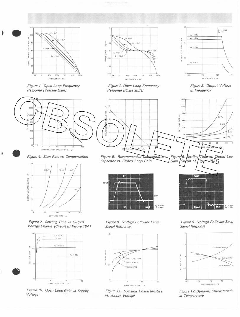
Figure 1. Open Loop FrequencyResponse (Voltage Gain)
t . COMPENSATION CAPACITOR Cc - pF
Figure 4. Slew Rate vs. Compensation
20
>., 15I"z~~ 1000>~'"
§ 5
a0 50 200
SETTLING TIME -",
Figure 7. Settling Time vs. OutputVoltage Change (Circuit of Figure 18A)
110
~100z~"c:~00> 90
TA 0 "25"C
R, > lOk
880
5 10 15 20
SUPPL Y VOLTAGE -;v
Figure 10. Open Loop Gain vs. SupplyVoltage
45
~ -45<':
I
~ -90I~
~ -135
-180
-225100 lk lOk lOOk
FREOUENCY - H,
Figure 2. Open Loop FrequencyResponse (Phase Shift)
14
'!i 12I
2'0~j 8z0~ 6~"40u
Ol1 100
Figure 5. Recommended CompensationCapacitor vs. Closed Loop Gain
INPUT
R, =1000Cc~ 20pF
OUT
Figure 8. Voltage Follower LargeSignal Response
1.5
~
~>
§::: 05
SLEW RATE
05 10 15 20
SUPPLYVOlTAGE-,V
Figure 11. Dynamic Characteristicsvs. Supply Voltage
")
---
30
0lOOk 1M 10M 10
FREOUENCY - H,
Figure 3. Output Voltage
vs. Frequency
1200
1000
C 800I
200
ol1 10 20
CLOSED LOOP GAIN - -vlV
Figure 6. Settling Time vs. Closed LoaGain (Circuit of Figure 18A)
Figure 9. Voltage Follower SmalSignal Response
1.S
SETTLING TIME
~
~>
~~g 0.5
0-75 -2S '2S "5
TEMPERATURE-"c
"
Figure 12. Dynamic Characteristh
vs. Temperature
- ~-- - - -
100'"I
80":'5
6000>
§ 40zw
15 20
a100 1k
OBSOLETE
~I
15 3
~~0 2'"1i~
OL0 25 50 75
TEMPERATURE- °c
125
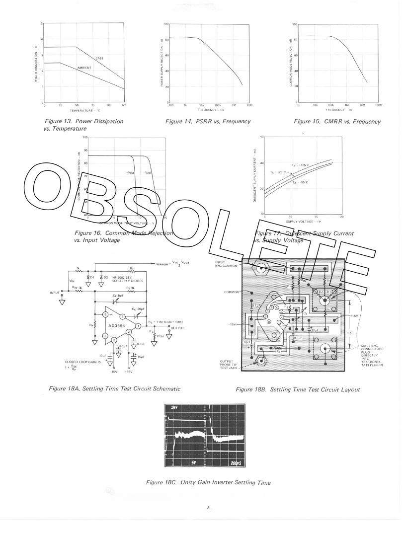
Figure 13. Power Dissipationvs. Temperature
100
90'"~I
Z:=: 80
~'" 70
~0"15 60""0u
400
CDMMON MODE INPUT VOL TAGE - V
100
'"80I
15
i60>~
~ 40'"1i0~ 20
0100 1k IOk lOOk
FREDUENCY - H,1M
Figure 14. PSRR vs. Frequency
Figure 16. Common Mode Rejectionvs. Input Voltage
1k lk
V,N
A'N 3k
D2 HP 5082.2811SCHOTTKY DIODES
AF 3k
INPUT~
Rp
CLOSED LOOP GAIN IS
1 + AINRP -15V +15V
VERROR 0 VI"; VOUTINPUTBNC COMMON
RL 0 115111k1l3k 0 100"-15V
OUTPUT
Ad .1..115" "\1
OUTPUTPAOBE TIPTEST JACK
Figure 18A. Settling Time Test Circuit Schematic
100
'"80I
15
i60
~§!40
15""0u 20
10M01k 100M10k lOOk 1M 10M
FREOUENCY - H,
Figure 15. CMRR vs. Frequency
40
<{EI
!2
! 30>~~=>00
~ 20:;0
105 10 15
SUPPLYVOLTAGE-'V
20
Figure 17. Quiescent Supply Currentvs. Supply Voltage
MALE BNCCONNECTOASPLUGDIAECTLYINTOTEKTADNIX7ABPLUGIN
Figure 188. Settling Time Test Circuit Layout
Figure 18C. Unity Gain Inverter Settling Time
.A-
OBSOLETE
"'" H UI"L\.."""'~ UH;; 11~"" VI V~'-lWH1VlI UUC: LV lIll:rc:a:sc:u pnnIC:u
circuit board capacitance.
I
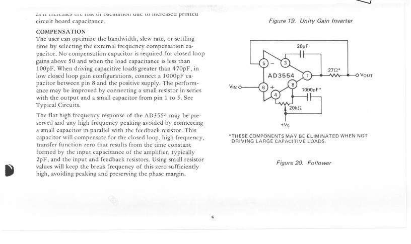
COMPENSA nON
The user can optimize the bandwidth, slew rate, or settlingtime by selecting the external frequency compensation ca-pacitor. No compensation capacitor is required for closed loopgains above 50 and when the load capacitance is less than1OOpF. When driving capacitive loads greater than 4 70pF, inlow closed loop gain configurations, connect a 1000pF ca-pacitor between pin 8 and the positive supply. The perform-ance may be improved by connecting a small resistor in serieswith the output and a small capacitor from pin 1 to 5. SeeTypical Circuits.
The flat high frequency response of the AD3554 may be pre-served and any high frequency peaking avoided by connectinga small capacitor in parallel with the feedback resistor. Thiscapacitor will compensate for the closed loop, high frequency,transfer function zero that results from the time constant
formed by the input capacitance of the amplifier, typically2pF, and the input and feedback resistors. Using small resistorvalues will keep the break frequency of this zero sufficientlyhigh, avoiding peaking and preserving the phase margin.
-- --
Figure 19. Unity Gain Inverter
20pF
VIN
VOUT27D.*
+Vs
*THESE COMPONENTS MAY BE ELIMINATED WHEN NOTDRIVING LARGE CAPACITIVE LOADS.
Figure 20. Follower
t:
OBSOLETE
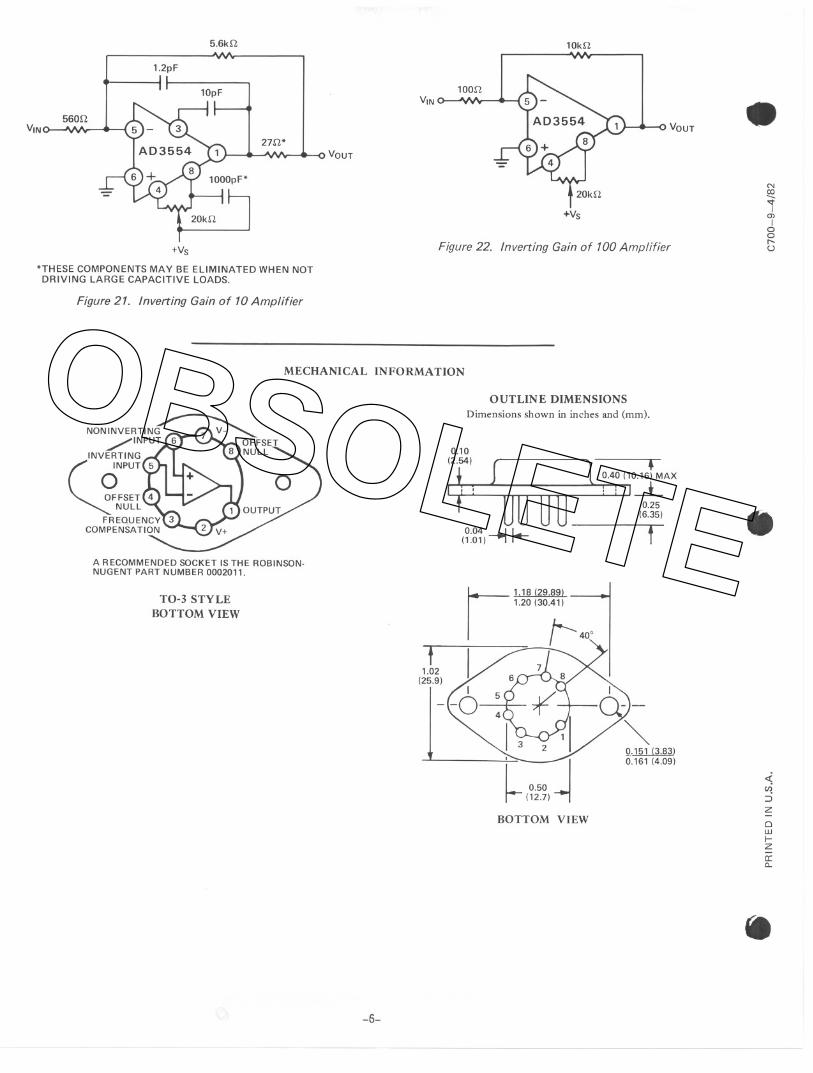
5.6kn
1.2pF
10pF
56on
27n*VIN
+Vs
*THESE COMPONENTS MAY BE ELIMINATED WHEN NOTDRIVING LARGE CAPACITIVE LOADS.
Figure 21. Inverting Gain of 10 Amplifier
VOUT
10kn
lOonVIN
+Vs
Figure 22. Inverting Gain of 100 Amplifier
MECHANICAL INFORMATION
A RECOMMENDED SOCKET IS THE ROBINSON-NUGENT PART NUMBER 0002011.
TO-3 STYLEBOTTOM VIEW
---
OUTLINE DIMENSIONSDimensionsshown in inches and (mm).
0.10
~0.04 I L..
(1.01)~ ~
~ .0.40 (10.16) MAX
" -L0.25
(6.35)
f
BOTTOM VIEW
-6-
VOUT -
('Jcol'0>I00r--U
.
<t;~:JZ0wI-Za:"-
at
OBSOLETE