Embed Size (px)
Citation preview
Observation of Strong Polarization Enhancement in FerroelectricTunnel JunctionsLinze Li,† Xiaoxing Cheng,‡ Thomas Blum,○ Huaixun Huyan,† Yi Zhang,† Colin Heikes,§
Xingxu Yan,† Chaitanya Gadre,○ Toshihiro Aoki,∥ Mingjie Xu,∥ Lin Xie,⊥ Zijian Hong,‡
Carolina Adamo,# Darrell G. Schlom,#,∇ Long-Qing Chen,‡ and Xiaoqing Pan*,†,∥,○
†Department of Chemical Engineering and Materials Science, University of California - Irvine, Irvine, California 92697, UnitedStates‡Department of Materials Science and Engineering, Pennsylvania State University, University Park, Pennsylvania 16802, UnitedStates○Department of Physics and Astronomy, University of California - Irvine, Irvine, California 92697, United States§NIST Center for Neutron Research, National Institute of Standards and Technology, Gaithersburg, Maryland 20899, United States∥Irvine Materials Research Institute (IMRI), University of California - Irvine, Irvine, California 92697, United States⊥National Laboratory of Solid State Microstructures and College of Engineering and Applied Sciences, Nanjing University, Nanjing,Jiangsu 210093, China#Department of Materials Science and Engineering, Cornell University, Ithaca, New York 14853, United States∇Kavli Institute at Cornell for Nanoscale Science, Ithaca, New York 14853, United States
*S Supporting Information
ABSTRACT: Ferroelectric heterostructures, with capability of storing data at ultrahigh densities, could act as the platform fornext-generation memories. The development of new device paradigms has been hampered by the long-standing notion ofinevitable ferroelectricity suppression under reduced dimensions. Despite recent experimental observation of stable polarizedstates in ferroelectric ultrathin films, the out-of-plane polarization components in these films are strongly attenuated comparedto thicker films, implying a degradation of device performance in electronic miniaturization processes. Here, in a model systemof BiFeO3/La0.7Sr0.3MnO3, we report observation of a dramatic out-of-plane polarization enhancement that occurs withdecreasing film thickness. Our electron microscopy analysis coupled with phase-field simulations reveals a polarization-enhancement mechanism that is dominated by the accumulation of oxygen vacancies at interfacial layers. The results shed lighton the interplay between polarization and defects in nanoscale ferroelectrics and suggest a route to enhance functionality inoxide devices.
KEYWORDS: Ferroelectric tunnel junctions, ultrathin films, polarization enhancement, oxygen vacancies,transmission electron microscopy
As the demand for scaling nonvolatile memories down toonly a few nanometers continues to increase, hetero-
structures based on ferroelectric oxides have emerged aspromising candidates to meet the requirements of low powerconsumption, fast write speed, large read/write cycleendurance, high density, and multilevel functionalities.1,2 One
prototype device that has recently drawn considerable interestis the ferroelectric tunnel junction (FTJ), in which an ultrathin
Received: May 7, 2019Revised: July 27, 2019Published: September 11, 2019
Letter
pubs.acs.org/NanoLettCite This: Nano Lett. 2019, 19, 6812−6818
© 2019 American Chemical Society 6812 DOI: 10.1021/acs.nanolett.9b01878Nano Lett. 2019, 19, 6812−6818
Dow
nloa
ded
via
NA
TL
IN
ST O
F ST
AN
DA
RD
S &
TE
CH
NO
LO
GY
on
Apr
il 21
, 202
0 at
16:
46:1
8 (U
TC
).Se
e ht
tps:
//pub
s.ac
s.or
g/sh
arin
ggui
delin
es f
or o
ptio
ns o
n ho
w to
legi
timat
ely
shar
e pu
blis
hed
artic
les.
ferroelectric film is sandwiched between two electrodes. Itsconductance is dominated by electronic tunneling through theultrathin film and can be modulated by reversing theferroelectric polarization with an applied electric field.3−5
Two different device configurations are frequently adopted inpractical FTJ devices. While the bottom electrode is usually anepitaxial conductive buffer layer embedded between aninsulating substrate and the ferroelectric layer, the topelectrode can be either a second conductive layer depositedabove the ferroelectric film or just a conductive probe that canmove arbitrarily at the free surface of the film.3,6 The latter caseis particularly attractive for nanodevice applications, as it allowsthe domain structures in the ferroelectric film to bemanipulated facilely and controllably by the mobile probeand thus permits an ultrahigh density of storage bits to bewritten.To gain a fundamental understanding of the polarization
structures in FTJ, a number of theoretical and experimentalstudies have explored the polarized states in ferroelectric thinfilms with varying thicknesses.7−12 A general observation is thatwith reduced film thickness, the out-of-plane polarization isinevitably suppressed due to enhanced depolarization effects.In some systems, a “critical thickness”, below which theferroelectric polarization is eliminated, also exists. For example,using electrical measurements, Kim et al. observed significantlyreduced polarization in BaTiO3 thin films between twometallic SrRuO3 electrodes when the films are <10 nm inthickness.7 From first-principles calculations Junquera andGhosez showed that BaTiO3 thin films between two SrRuO3electrodes lose their ferroelectricity when their thicknesses arebelow a critical value of ∼2.4 nm.8 Using piezoresponse forcemicroscopy (PFM) Maksymovych et al. detected weak signalsof ferroelectric switching in BiFeO3 ultrathin films grown onLa0.7Sr0.3MnO3 electrodes and predicted that the criticalthickness lies in the range from 1 to 2 nm.9 With in situoptical second harmonic generation (ISHG), De Luca et al.monitored the evolution of polarization states during the layer-by-layer growth of both BaTiO3 and BiFeO3 films on SrRuO3electrodes and found that ferroelectricity in both films does notemerge until the films are more than 4 unit cells in thickness.10
This observed polarization attenuation or annihilation inferroelectric ultrathin films would in principle lead to degradedperformance in FTJ devices, but numerous groups havereported very high tunnel electroresistance (TER) measuredfrom fabricated FTJ devices. Specifically, TER values as large as6.0 × 108 % are reported in a four-unit-cell BaTiO3-based FTJdevice,13 and TER of ∼2700% is reported in a two-unit-cellBiFeO3-based FTJ device.
14 Such measured giant TER requiresa significant and switchable out-of-plane polarization in theferroelectric ultrathin layer of the FTJ device. Therefore,although extensive research activity has been devoted to thetechnical exploration and fundamental understanding of FTJsystems, a gap still exists between the optimization of deviceconfigurations and the probing of polarization structures innanosized ferroelectrics. In particular, electrical measurementsof the polarization-field loops in ferroelectric ultrathin films arecomplicated by leakage or tunneling currents. Measurementswith PFM can only provide indirect, semiquantitative estimatesof the polarization and can be affected by several artifactsrelated with topographical features, background signals, ornonpiezoelectric effects.15 In situ SHG is conducted during filmgrowth at elevated temperatures and thus cannot directlyreflect the room-temperature properties of ferroelectric films.
First-principle calculations often must ignore local defects thatmay dominate the responses of real materials. It is thusnecessary to experimentally explore possible mechanisms ofpolarization enhancement in ferroelectric ultrathin films, at theatomic scale, to make full use of the technological potential ofFTJ devices.Recent advances in aberration-corrected scanning trans-
mission electron microscopy (STEM) have opened excitingopportunities for probing materials structures with sub-angstrom-level precision and have made it possible to directlymeasure the spatial distribution of polarization displacementvectors in a ferroelectric crystal at atomic scale.16 Using apolarization mapping technique based on atomic-resolutionSTEM, stable polarized states have been directly observed intetragonal PbTiO3 and Pb(Zr0.2Ti0.8)O3 films with only a fewunit cells in thickness or tetragonal-like (T-like) BiFeO3 filmswith thicknesses down to a single unit cell.17−19 Theirpolarization strength, however, is still greatly reducedcompared to thicker (>5−10 nm) tetragonal PbTiO3 orPb(Zr0.2Ti0.8)O3 films, or T-like BiFeO3 films, respec-tively.17,18,20 Enhanced polarization states stabilized by surfaceimpurity defects have also been observed in 2 nm-thick BiFeO3film.21 Nevertheless, the strong polarization-defect interactionmakes the polarization stable only when it is pointing to thedefect, and therefore the enhanced polarization state is almostcertainly nonswitchable. Here, we use aberration-correctedSTEM to exam the polarization structures in a model system offerroelectric heterostructures composed of ferroelectric BiFeO3films and La0.7Sr0.3MnO3 bottom electrodes. We show that,contrary to previous measurements in ferroelectric films, themagnitude of the out-of-plane polarization component in theBiFeO3 films does not decrease monotonically with thereduced film thickness, but instead presents an asymmetricbehavior for the two opposite polarized states. While thepolarization strength in the upward polarized domains isreduced with decreasing film thickness, the polarizationstrength in the downward polarized domains is surprisinglyenhanced to a great extent. This occurs with a concomitantrhombohedral-like-to-tetragonal-like structure transformationin the BiFeO3 film when its thickness reaches below a criticalvalue of ∼2 nm. Our STEM analysis coupled with electronenergy-loss spectroscopy (EELS) and phase-field simulationsreveal the critical nature of oxygen vacancy accumulation at theBiFeO3/La0.7Sr0.3MnO3 interface, which produces a strongbuilt-in field that can lead to the observed changes ofpolarization structures.BiFeO3 is a room-temperature multiferroic exhibiting
coupled ferroelectric (TC ∼ 1103 K) and antiferromagnetic(TN ∼ 650 K) order.22−24 Structures of epitaxial BiFeO3 filmsare correlated to the misfit strain imposed by their underlyingsubstrates. BiFeO3 films with moderate tensile or compressive(< ∼ 4.5%) strain are usually monoclinically distorted, butclosely resemble the bulk rhombohedral phase, and aretherefore referred to as “rhombohedral-like (R-like)” struc-tures.25 In pseudocubic unit cells of the R-like structure(Figure 1a), the oxygen octahedra and the central Fe cation aredisplaced from their respective positions at the face and bodycenters, giving rise to a large spontaneous polarization (∼100μC cm−2) along the ⟨111⟩PC directions,22−24,26,27 where thePC subscript represents pseudocubic indices. Under a largecompressive epitaxial strain exceeding ∼4.5%, BiFeO3 can alsobe stabilized into a monoclinic structure that is T-like.25 In theT-like structure (Figure 1a), the Fe atom is five-coordinated,
Nano Letters Letter
DOI: 10.1021/acs.nanolett.9b01878Nano Lett. 2019, 19, 6812−6818
6813
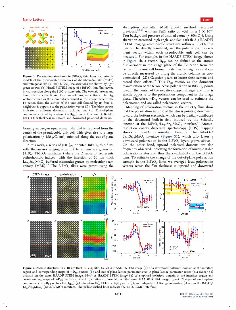
forming an oxygen square-pyramidal that is displaced from thecenter of the pseudocubic unit cell. This gives rise to a largepolarization (∼150 μC/cm2) oriented along the out-of-planedirection.In this work, a series of (001)PC oriented BiFeO3 thin films
with thicknesses ranging from 1.2 to 20 nm are grown on(110)O TbScO3 substrates (where the O subscript representsorthorhombic indices) with the insertion of 20 nm thickLa0.7Sr0.3MnO3 buffered electrodes grown by molecular-beamepitaxy (MBE).28 The BiFeO3 films were grown using the
absorption controlled MBE growth method describedpreviously29,30 with an Fe:Bi ratio of ∼5:1 in a 5 × 10⁻⁶
Torr background pressure of distilled ozone (∼80% O3). Usingaberration-corrected high-angle annular dark-field (HAADF)STEM imaging, atomic-scale structures within a BiFeO3 thinfilm can be directly visualized, and the polarization displace-ment vector within each pseudocubic unit cell can bemeasured. For example, in the HAADF STEM image shownin Figure 1b, a vector, DFB, can be defined as the atomicdisplacement in the image plane of the Fe cation from thecenter of the unit cell formed by its four Bi neighbors and canbe directly measured by fitting the atomic columns as two-dimensional (2D) Gaussian peaks to locate their centers andrecord their offsets.16 This DFB vector, as the dominantmanifestation of the ferroelectric polarization in BiFeO3, pointstoward the center of the negative oxygen charges and thus isexactly opposite to the polarization component in the imageplane. Therefore, −DFB vectors can be used to estimate thepolarization and are called polarization vectors.Mapping of polarization vectors in the BiFeO3 films show
that the polarization in most of the film is pointing downward,toward the bottom electrode, which can be partially attributedto the downward built-in field induced by the Schottkyjunction at the BiFeO3/La0.7Sr0.3MnO3 interface.31 Atomic-resolution energy dispersive spectroscopy (EDS) mappingshows a Fe−O2 termination layer at the BiFeO3/La0.7Sr0.3MnO3 interface (Figure S1), which also favors adownward polarization in the BiFeO3 layers grown above.10
On the other hand, upward polarized domains are alsofrequently observed, indicating the formation of multiple stablepolarization states and thus the switchability of the BiFeO3films. To estimate the change of the out-of-plane polarizationstrength in the BiFeO3 films, we averaged local polarizationvectors across the film thickness in upward and downward
Figure 1. Polarization structures in BiFeO3 thin films. (a) Atomicmodels of the pseudocubic structures of rhombohedral-like (R-like)and tetragonal-like (T-like) BiFeO3. Polarizations are shown by lightgreen arrows. (b) HAADF STEM image of a BiFeO3 thin film viewedin cross-section along the [100]PC zone axis. The overlaid brown andblue balls mark the Bi and Fe atom columns, respectively. The DFBvector, defined as the atomic displacement in the image plane of theFe cation from the center of the unit cell formed by its four Bineighbors, is opposite to the polarization vector (P). The black arrowsindicate a uniform downward polarization. (c) Out-of-planecomponents of −DFB vectors (|−DFB|z) as a function of BiFeO3(BFO) film thickness in upward and downward polarized domains.
Figure 2. Atomic structures in a 10 nm-thick BiFeO3 film. (a−c) A HAADF STEM image (a) of a downward polarized domain at the interfaceregion and corresponding maps of −DFB vectors (b) and out-of-plane lattice parameter over in-plane lattice parameter ratios (c/a ratios) (c)overlaid on the same HAADF STEM image. (d−f) A HAADF STEM image (a) of a upward polarized domain at the interface region andcorresponding maps of −DFB vectors (b) and c/a ratios (c) overlaid on the same HAADF STEM image. (g−j) Changes of out-of-planecomponents of −DFB vectors (|−DFB|z) (g), c/a ratios (h), EELS Fe L3/L2 ratios (i), and integrated O K-edge intensities (j) across the BiFeO3/La0.7Sr0.3MnO3 (BFO/LSMO) interface. The yellow dashed lines indicate the BFO/LSMO interface.
Nano Letters Letter
DOI: 10.1021/acs.nanolett.9b01878Nano Lett. 2019, 19, 6812−6818
6814
polarized domains, respectively, in each BiFeO3 film. In Figure1c, we plot the average magnitude of the out-of-planepolarization vectors (|−DFB|z) as a function of the filmthickness. The observed polarization attenuation with thereduced film thickness in the upward polarized domains iscommonly expected as a result of an enhanced depolarizationfield arising from interface boundary conditions.8 However, theanomalous polarization enhancement with the reduced filmthickness in the downward polarized domains is counter-intuitive and directly opposite to the correlation betweenferroelectric polarization and film thickness reported inprevious studies.7−12 Based on an assumed linear relationshipbetween the ferroelectric polarization (PS) and the −DFBvectors,16 the out-of-plane polarization strength is estimatedto be 59 uC/cm2 in the 20 nm BiFeO3 film and increases to 72uC/cm2 and 105 uC/cm2 in the 5 and 1.2 nm BiFeO3 films,respectively.To explain the asymmetric trends observed for the two
opposite polarization states, it is necessary to examine theatomic-scale polarization distribution in the BiFeO3 films. Wefirst show the results of a 10 nm BiFeO3 film, in which typicalR-like crystal structures are observed. The HAADF STEMimages and corresponding maps of polarization vectors andlattice parameters of two local regions across the BiFeO3/La0.7Sr0.3MnO3 interface with upward and downward polar-ization states are shown in Figure 2a−c and d−f, respectively.By averaging the data from each lattice layer, the change of thelattice parameters and the magnitude of out-of-plane polar-ization vectors (|−DFB|z) for the upward and downwardpolarized domains is plotted in Figure 2g,h, respectively. Themost remarkable feature is a change of both polarization andlattice parameters at the interfacial region in the BiFeO3 filmthat extends four-unit cells from the interface. While thepolarization vectors are clearly attenuated at the interfacialregion of the upward polarized domain (Figure 2e), noapparent polarization suppression is observed at the interfacialregion of the downward polarized domain (Figure 2b), andinstead, the local polarization vectors there slightly rotate intothe out-of-plane direction. As a result, the magnitudes of out-of-plane polarization vectors at the interfacial region in theupward polarized domain are significantly reduced, but thosein the downward polarized domain are slightly enhanced(Figure 2g). In contrast, the mapping results in Figure 2c,f,hsimilarly show an increase in the out-of-plane lattice parameterover in-plane lattice parameter ratio (c/a) at the interfacialregions of both domains.
The changes of polarization and lattice structures at theinterfacial regions could be correlated to local variations ofchemical profiles and oxidation states across the BiFeO3/La0.7Sr0.3MnO3 interface, as evidenced by our EELS study.Figure 2i,j shows average profiles of the L3/L2 ratios for the Feand Mn L3,2-edges and average profiles of the integrated O K-edge intensities, respectively, where similar trends are observedfor the two interface regions with opposite polarizationorientations. By comparing the measured L3/L2 values to thereference values marked with the yellow (Fe) and blue (Mn)bands (Figure 2i), the changes of the cations’ valence statescan be estimated.32 While away from the interface, Fe and Mnhave valence states of ∼ +3 that are close to the bulk value;lower valence states of both elements are observed within theinterfacial layers that include three unit cells above and oneunit cell below the interface. In the corresponding EELSspectra shown in Figures S2 and S3, the L3 peaks of both Feand Mn shift to lower-energy positions at the interfacial region,which is also an indication of local valence decrease of thesetransition metals. The reduction of cation valences inperovskites is usually associated with strong local accumulationof oxygen vacancies, which is indeed consistent with theapparent oxygen depletion at the interfacial layers, as revealedby the profiles of the O K-edge intensities in Figure 2j. Areduced cation valence in general leads to an increased radiusof cations and thus to a lattice expansion in perovskiteoxides.33−35 In epitaxial thin films, as the in-plane latticeparameters are constrained by the substrate, the latticeexpansion mostly occurs through the out-of-plane elongation.In fact, formation of oxygen vacancies at heterostructureinterfaces has been observed in several different ferroelectricsystems, and it has been shown that these vacancies can causelocal out-of-plane lattice elongation.32,36−38 This is consistentwith our finding of enhanced c/a ratios at the interfacialregions of the 10 nm-thick BiFeO3 film (Figure 2c,f,h).To further illustrate the effects of interfacial oxygen
vacancies, in Figure S4 we show the maps of polarizationvectors and lattice parameters across a local BiFeO3/La0.7Sr0.3MnO3 interface with downward polarization, inwhich strong accumulation of oxygen vacancies is not observedaccording to EELS analysis of transition-metal valences and Ointensities (Figures S4 and S5). Of note, such a type ofinterface has been rarely observed in our BiFeO3 films, as thedominant type shows a much stronger oxygen vacancyaccumulation as discussed above. Here, the polarizationstrength gradually reduces from the inner region of the
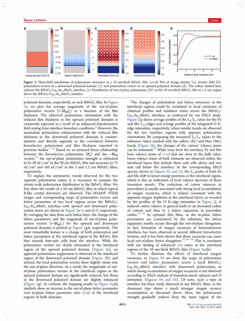
Figure 3. Phase-field simulations of polarization structures in a 10 nm-thick BiFeO3 film. (a−d) Plot of charge density (a), electric field (b),polarization vectors in a downward polarized domain (c), and polarization vectors in an upward polarized domain (d). The yellow dashed linesindicate the BiFeO3/La0.7Sr0.3MnO3 interface. (e) Distribution of out-of-plane polarization (Pz) in the 10 nm-thick BiFeO3 film in a 5 nm regionabove the BiFeO3/La0.7Sr0.3MnO3 interface.
Nano Letters Letter
DOI: 10.1021/acs.nanolett.9b01878Nano Lett. 2019, 19, 6812−6818
6815
BiFeO3 film to the interface (Figure S4b,d), and the c/a ratiosat the interfacial regions are not apparently enhancedcompared to the inner film (Figure S4c,e). Through thecomparison between the two types of interfaces, the criticaleffects of interfacial accumulation of oxygen vacancies on thepolarization structures can be deduced. Such interface effectsbecome more prominent as the film thickness decreases. In thecase of a 5 nm BiFeO3 film, this leads to an overall polarizationenhancement/suppression in the downward/upward polarizeddomains, respectively (Figure S6).Phase-field simulations allow the effect of the charge
distribution induced by the accumulation of oxygen vacanciesat the interfacial region to be studied. Such accumulation ofoxygen vacancies should results in a positively charged layer ofseveral unit cells in thickness in the semiconducting BiFeO3film above the interface, and consequentially an atomicallythin, negatively charged, free charge compensation layer at thesurface of the metallic La0.7Sr0.3MnO3 film. In a simulated 10nm BiFeO3 film on a La0.7Sr0.3MnO3 substrate, we appliedpositive charge densities ranging from 0.26 × 10⁹ C/m3 to 2.08× 10⁹ C/m3 at a 2 nm-thick interfacial layer in the BiFeO3 filmabove the interface and maintained a total zero net chargeacross the heterojunction by applying corresponding negativecharge densities ranging from −1.3 × 10⁹ C/m3 to −1.04 ×10¹⁰ C/m3 at the surface of the La0.7Sr0.3MnO3 layer. In Figure3c,d, the calculated stable polarization structures with a chargedensity of 0.78 × 10⁹ C/m3 at the interfacial layer of theBiFeO3 film show apparent polarization suppression at theinterfacial region of the upward polarized domain andpolarization enhancement at the interfacial region of thedownward polarized domain, whereas the polarization in theupper portion of the film remains mostly unperturbed. Thissituation is most consistent with the experimental observationin Figure 2. The origin of the changes of polarization structuresis the built-in electric field (Figure 3b) introduced by thecharge distribution (Figure 3a) at the interfacial layers. Thephase-field simulations thus confirm the important role of theelectrostatic boundary conditions at the interface in bothpolarization states.The situation for the coupling between accumulation of
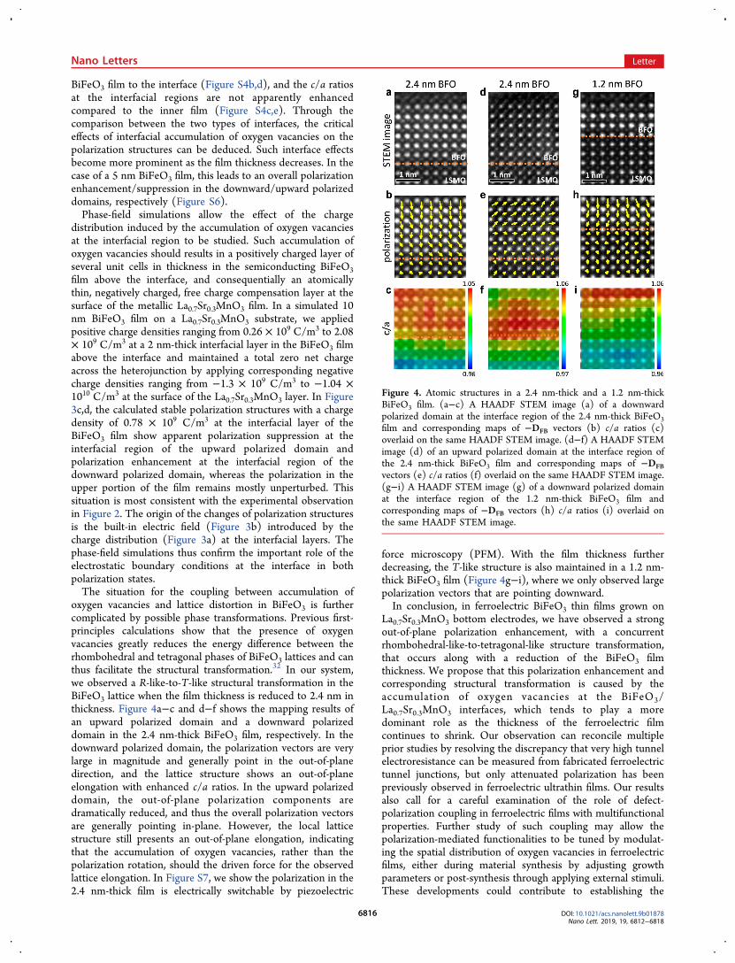
oxygen vacancies and lattice distortion in BiFeO3 is furthercomplicated by possible phase transformations. Previous first-principles calculations show that the presence of oxygenvacancies greatly reduces the energy difference between therhombohedral and tetragonal phases of BiFeO3 lattices and canthus facilitate the structural transformation.32 In our system,we observed a R-like-to-T-like structural transformation in theBiFeO3 lattice when the film thickness is reduced to 2.4 nm inthickness. Figure 4a−c and d−f shows the mapping results ofan upward polarized domain and a downward polarizeddomain in the 2.4 nm-thick BiFeO3 film, respectively. In thedownward polarized domain, the polarization vectors are verylarge in magnitude and generally point in the out-of-planedirection, and the lattice structure shows an out-of-planeelongation with enhanced c/a ratios. In the upward polarizeddomain, the out-of-plane polarization components aredramatically reduced, and thus the overall polarization vectorsare generally pointing in-plane. However, the local latticestructure still presents an out-of-plane elongation, indicatingthat the accumulation of oxygen vacancies, rather than thepolarization rotation, should the driven force for the observedlattice elongation. In Figure S7, we show the polarization in the2.4 nm-thick film is electrically switchable by piezoelectric
force microscopy (PFM). With the film thickness furtherdecreasing, the T-like structure is also maintained in a 1.2 nm-thick BiFeO3 film (Figure 4g−i), where we only observed largepolarization vectors that are pointing downward.In conclusion, in ferroelectric BiFeO3 thin films grown on
La0.7Sr0.3MnO3 bottom electrodes, we have observed a strongout-of-plane polarization enhancement, with a concurrentrhombohedral-like-to-tetragonal-like structure transformation,that occurs along with a reduction of the BiFeO3 filmthickness. We propose that this polarization enhancement andcorresponding structural transformation is caused by theaccumulation of oxygen vacancies at the BiFeO3/La0.7Sr0.3MnO3 interfaces, which tends to play a moredominant role as the thickness of the ferroelectric filmcontinues to shrink. Our observation can reconcile multipleprior studies by resolving the discrepancy that very high tunnelelectroresistance can be measured from fabricated ferroelectrictunnel junctions, but only attenuated polarization has beenpreviously observed in ferroelectric ultrathin films. Our resultsalso call for a careful examination of the role of defect-polarization coupling in ferroelectric films with multifunctionalproperties. Further study of such coupling may allow thepolarization-mediated functionalities to be tuned by modulat-ing the spatial distribution of oxygen vacancies in ferroelectricfilms, either during material synthesis by adjusting growthparameters or post-synthesis through applying external stimuli.These developments could contribute to establishing the
Figure 4. Atomic structures in a 2.4 nm-thick and a 1.2 nm-thickBiFeO3 film. (a−c) A HAADF STEM image (a) of a downwardpolarized domain at the interface region of the 2.4 nm-thick BiFeO3film and corresponding maps of −DFB vectors (b) c/a ratios (c)overlaid on the same HAADF STEM image. (d−f) A HAADF STEMimage (d) of an upward polarized domain at the interface region ofthe 2.4 nm-thick BiFeO3 film and corresponding maps of −DFBvectors (e) c/a ratios (f) overlaid on the same HAADF STEM image.(g−i) A HAADF STEM image (g) of a downward polarized domainat the interface region of the 1.2 nm-thick BiFeO3 film andcorresponding maps of −DFB vectors (h) c/a ratios (i) overlaid onthe same HAADF STEM image.
Nano Letters Letter
DOI: 10.1021/acs.nanolett.9b01878Nano Lett. 2019, 19, 6812−6818
6816
design paradigm for next-generation ferroelectric-basedreconfigurable electronic nanodevices.
■ ASSOCIATED CONTENT*S Supporting InformationThe Supporting Information is available free of charge on theACS Publications website at DOI: 10.1021/acs.nano-lett.9b01878.
Film growth; transmission electron microscopy; phase-field simulations; and discussion on PFM results (PDF)
■ AUTHOR INFORMATIONCorresponding Author*E-mail: [email protected] Li: 0000-0001-5362-8991Xingxu Yan: 0000-0001-7991-4849Xiaoqing Pan: 0000-0002-0965-8568NotesThe authors declare no competing financial interest.
■ ACKNOWLEDGMENTSThe experimental work was mainly supported by theDepartment of Energy (DOE) under grant DE-SC0014430(L.Z.L., T.B., H.H, X.X.Y., C.G., T.A., M.J.X., L.X., andX.Q.P.). The TEM work was conducted at the Irvine MaterialsResearch Institute at University of California, Irvine. Thetheoretical work at the Pennsylvania State University wassupported by the U.S. Department of Energy, Office of BasicEnergy Sciences, Division of Materials Sciences and Engineer-ing under award FG0207ER46417 (X.X.C., Z.J.H., andL.Q.C.). Calculations at the Pennsylvania State Universitywere performed on the Cyberstar Linux Cluster funded by theNational Science Foundation through grant OCI0821527. Thework at Cornell University was supported by the NationalScience Foundation (Nanosystems Engineering ResearchCenter for Translational Applications of Nanoscale Multi-ferroic Systems) under grant number EEC-1160504 (C.H.,C.A., and D.G.S.). This work was performed in part at theCornell Nanoscale Facility, a member of the NationalNanotechnology Coordinated Infrastructure (NNCI), whichis supported by the National Science Foundation (grantECCS-1542081).
■ REFERENCES(1) Scott, J. F. Applications of modern ferroelectrics. Science 2007,315, 954−959.(2) Hu, J. M.; Duan, C. G.; Nan, C. W.; Chen, L. Q. Understandingand designing magnetoelectric heterostructures guided by computa-tion: progresses, remaining questions, and perspectives. Npj Computa-tional Materials 2017, 3, 18.(3) Garcia, V.; Fusil, S.; Bouzehouane, K.; Enouz-Vedrenne, S.;Mathur, N. D.; Barthelemy, A.; Bibes, M. Giant tunnel electro-resistance for non-destructive readout of ferroelectric states. Nature2009, 460, 81−84.(4) Gajek, M.; Bibes, M.; Fusil, S.; Bouzehouane, K.; Fontcuberta, J.;Barthelemy, A. E.; Fert, A. Tunnel junctions with multiferroic barriers.Nat. Mater. 2007, 6, 296−302.(5) Velev, J. P.; Burton, J. D.; Zhuravlev, M. Y.; Tsymbal, E. Y.Predictive modelling of ferroelectric tunnel junctions. Npj Computa-tional Materials 2016, 2, 16009.(6) Garcia, V.; Bibes, M. Ferroelectric tunnel junctions forinformation storage and processing. Nat. Commun. 2014, 5, 4289.
(7) Kim, Y. S.; Kim, D. H.; Kim, J. D.; Chang, Y. J.; Noh, T. W.;Kong, J. H.; Char, K.; Park, Y. D.; Bu, S. D.; Yoon, J. G.; Chung, J. S.Critical thickness of ultrathin ferroelectric BaTiO3 films. Appl. Phys.Lett. 2005, 86, 102907.(8) Junquera, J.; Ghosez, P. Critical thickness for ferroelectricity inperovskite ultrathin films. Nature 2003, 422, 506−509.(9) Maksymovych, P.; Huijben, M.; Pan, M. H.; Jesse, S.; Balke, N.;Chu, Y. H.; Chang, H. J.; Borisevich, A. Y.; Baddorf, A. P.; Rijnders,G.; Blank, D. H. A.; Ramesh, R.; Kalinin, S. V. Ultrathin limit anddead-layer effects in local polarization switching of BiFeO3. Phys. Rev.B: Condens. Matter Mater. Phys. 2012, 85, 014119.(10) De Luca, G.; Strkalj, N.; Manz, S.; Bouillet, C.; Fiebig, M.;Trassin, M. Nanoscale design of polarization in ultrathin ferroelectricheterostructures. Nat. Commun. 2017, 8, 1419.(11) Fong, D. D.; Stephenson, G. B.; Streiffer, S. K.; Eastman, J. A.;Auciello, O.; Fuoss, P. H.; Thompson, C. Ferroelectricity in ultrathinperovskite films. Science 2004, 304, 1650−1653.(12) Rault, J. E.; Ren, W.; Prosandeev, S.; Lisenkov, S.; Sando, D.;Fusil, S.; Bibes, M.; Barthelemy, A.; Bellaiche, L.; Barrett, N.Thickness-Dependent Polarization of Strained BiFeO3 Films withConstant Tetragonality. Phys. Rev. Lett. 2012, 109, 267601.(13) Xi, Z. N.; Ruan, J. J.; Li, C.; Zheng, C. Y.; Wen, Z.; Dai, J. Y.; Li,A. D.; Wu, D. Giant tunnelling electroresistance in metal/ferro-electric/semiconductor tunnel junctions by engineering the Schottkybarrier. Nat. Commun. 2017, 8, 15217.(14) Yoong, H. Y.; Wang, H.; Xiao, J.; Guo, R.; Yang, P.; Yang, Y.;Lim, S. T.; Wang, J.; Venkatesan, T.; Chen, J. Tunnelingelectroresistance effect in ultrathin BiFeO3-based ferroelectrictunneling junctions. Appl. Phys. Lett. 2016, 109, 242901.(15) Seol, D.; Kim, B.; Kim, Y. Non-piezoelectric effects inpiezoresponse force microscopy. Curr. Appl. Phys. 2017, 17, 661−674.(16) Nelson, C. T.; Winchester, B.; Zhang, Y.; Kim, S. J.; Melville,A.; Adamo, C.; Folkman, C. M.; Baek, S. H.; Eom, C. B.; Schlom, D.G.; Chen, L. Q.; Pan, X. Q. Spontaneous vortex nanodomain arrays atferroelectric heterointerfaces. Nano Lett. 2011, 11, 828−834.(17) Gao, P.; Zhang, Z. Y.; Li, M. Q.; Ishikawa, R.; Feng, B.; Liu, H.J.; Huang, Y. L.; Shibata, N.; Ma, X. M.; Chen, S. L.; Zhang, J. M.; Liu,K. H.; Wang, E. G.; Yu, D. P.; Liao, L.; Chu, Y. H.; Ikuhara, Y.Possible absence of critical thickness and size effect in ultrathinperovskite ferroelectric films. Nat. Commun. 2017, 8, 15549.(18) Zhang, S. R.; Zhu, Y. L.; Tang, Y. L.; Liu, Y.; Li, S.; Han, M. J.;Ma, J. Y.; Wu, B.; Chen, Z. H.; Saremi, S.; Ma, X. L. GiantPolarization Sustainability in Ultrathin Ferroelectric Films Stabilizedby Charge Transfer. Adv. Mater. 2017, 29, 1703543.(19) Wang, H.; Liu, Z. R.; Yoong, H. Y.; Paudel, T. R.; Xiao, J. X.;Guo, R.; Lin, W. N.; Yang, P.; Wang, J.; Chow, G. M.; Venkatesan, T.;Tsymbal, E. Y.; Tian, H.; Chen, J. S. Direct observation of room-temperature out-of-plane ferroelectricity and tunneling electro-resistance at the two-dimensional limit. Nat. Commun. 2018, 9, 3319.(20) Rossell, M. D.; Erni, R.; Prange, M. P.; Idrobo, J. C.; Luo, W.;Zeches, R. J.; Pantelides, S. T.; Ramesh, R. Atomic Structure of HighlyStrained BiFeO3 Thin Films. Phys. Rev. Lett. 2012, 108, 047601.(21) Xie, L.; Li, L. Z.; Heikes, C. A.; Zhang, Y.; Hong, Z. J.; Gao, P.;Nelson, C. T.; Xue, F.; Kioupakis, E.; Chen, L. Q.; Schlom, D. G.;Wang, P.; Pan, X. Q. Giant Ferroelectric Polarization in UltrathinFerroelectrics via Boundary-Condition Engineering. Adv. Mater. 2017,29, 1701475.(22) Zavaliche, F.; Yang, S. Y.; Zhao, T.; Chu, Y. H.; Cruz, M. P.;Eom, C. B.; Ramesh, R. Multiferroic BiFeO3 films: domain structureand polarization dynamics. Phase Transitions 2006, 79, 991−1017.(23) Chu, Y. H.; Martin, L. W.; Holcomb, M. B.; Ramesh, R.Controlling magnetism with multiferroics. Mater. Today 2007, 10,16−23.(24) Catalan, G.; Scott, J. F. Physics and Applications of BismuthFerrite. Adv. Mater. 2009, 21, 2463−2485.(25) Christen, H. M.; Nam, J. H.; Kim, H. S.; Hatt, A. J.; Spaldin, N.A. Stress-induced R-M-A-M-C-T symmetry changes in BiFeO3 films.Phys. Rev. B: Condens. Matter Mater. Phys. 2011, 83, 144107.
Nano Letters Letter
DOI: 10.1021/acs.nanolett.9b01878Nano Lett. 2019, 19, 6812−6818
6817
(26) Das, R. R.; Kim, D. M.; Baek, S. H.; Eom, C. B.; Zavaliche, F.;Yang, S. Y.; Ramesh, R.; Chen, Y. B.; Pan, X. Q.; Ke, X.; Rzchowski,M. S.; Streiffer, S. K. Synthesis and ferroelectric properties of epitaxialBiFeO3 thin films grown by sputtering. Appl. Phys. Lett. 2006, 88,242904.(27) Kubel, F.; Schmid, H. Structure of a ferroelectric andferroelastic monodomain crystal of the perovskite BiFeO3. ActaCrystallogr., Sect. B: Struct. Sci. 1990, 46, 698−702.(28) Adamo, C.; Ke, X.; Wang, H. Q.; Xin, H. L.; Heeg, T.; Hawley,M. E.; Zander, W.; Schubert, J.; Schiffer, P.; Muller, D. A.; Maritato,L.; Schlom, D. G. Effect of Biaxial Strain on the Electrical andMagnetic Properties of (001) La0.7Sr0.3MnO3 Thin Films. Appl.Phys. Lett. 2009, 95, 112504.(29) Smith, E. H.; Ihlefeld, J. F.; Heikes, C. A.; Paik, H. J.; Nie, Y. F.;Adamo, C.; Heeg, T.; Liu, Z. K.; Schlom, D. G. Exploiting kineticsand thermodynamics to grow phase-pure complex oxides bymolecular-beam epitaxy under continuous codeposition. PhysicalReview Materials 2017, 1, 023403.(30) Mundy, J. A.; Heikes, C. A.; Grosso, B. F.; Ferenc Segedin, D.;Wang, Z.; Goodge, B. H.; Meier, Q. N.; Nelson, C. T.; Prasad, B.;Kourkoutis, L. F.; Ratcliff, W. D.; Spaldin, N. A.; Ramesh, R.; Schlom,D. G. A high-energy density antiferroelectric made by interfacialelectrostatic engineering. arXiv e-prints, 2018. https://arxiv.org/ftp/arxiv/papers/1812/1812.09615.pdf.(31) Nelson, C. T.; Gao, P.; Jokisaari, J. R.; Heikes, C.; Adamo, C.;Melville, A.; Baek, S. H.; Folkman, C. M.; Winchester, B.; Gu, Y. J.;Liu, Y. M.; Zhang, K.; Wang, E. G.; Li, J. Y.; Chen, L. Q.; Eom, C. B.;Schlom, D. G.; Pan, X. Q. Domain dynamics during ferroelectricswitching. Science 2011, 334, 968−971.(32) Kim, Y. M.; Morozovska, A.; Eliseev, E.; Oxley, M. P.; Mishra,R.; Selbach, S. M.; Grande, T.; Pantelides, S. T.; Kalinin, S. V.;Borisevich, A. Y. Direct observation of ferroelectric field effect andvacancy-controlled screening at the BiFeO3/LaxSr1‑xMnO3 interface.Nat. Mater. 2014, 13, 1019−1025.(33) Mi, S. B.; Jia, C. L.; Heeg, T.; Trithaveesak, O.; Schubert, J.;Urban, K. Heterostructures of BaTiO3 bilayer films grown on SrTiO3(001) under different oxygen pressures. J. Cryst. Growth 2005, 283,425−430.(34) Cai, H. L.; Wu, X. S.; Gao, J. Effect of oxygen content onstructural and transport properties in SrTiO3‑x thin films. Chem. Phys.Lett. 2009, 467, 313−317.(35) Enriquez, E.; Chen, A. P.; Harrell, Z.; Dowden, P.; Koskelo, N.;Roback, J.; Janoschek, M.; Chen, C. L.; Jia, Q. X. Oxygen Vacancy-Tuned Physical Properties in Perovskite Thin Films with Multiple B-site Valance States. Sci. Rep. 2017, 7, 46184.(36) Catrou, P.; Tricot, S.; Delhaye, G.; Le Breton, J. C.; Turban, P.;Lepine, B.; Schieffer, P. Effect of oxygen vacancies at the Fe/SrTiO3(001) interface: Schottky barrier and surface electron accumulationlayer. Phys. Rev. B: Condens. Matter Mater. Phys. 2018, 98, 115402.(37) Matsuo, H.; Kitanaka, Y.; Inoue, R.; Noguchi, Y.; Miyayama, M.Cooperative effect of oxygen-vacancy-rich layer and ferroelectricpolarization on photovoltaic properties in BiFeO3 thin film capacitors.Appl. Phys. Lett. 2016, 108, 032901.(38) Matsuo, H.; Kitanaka, Y.; Noguchi, Y.; Miyayama, M. Stronginteraction between ferroelectric polarization and oxygen vacancy inBiFeO3 thin film capacitors. J. Ceram. Soc. Jpn. 2016, 124, 634−638.
Nano Letters Letter
DOI: 10.1021/acs.nanolett.9b01878Nano Lett. 2019, 19, 6812−6818
6818
![Observation of Polarization Vortices in Momentum Space · the vortices on them, homemade polarization-resolved momentum-space imaging spectroscopy based on Fourier analysis [35] was](https://img.pdfslide.us/doc/110x75/5e70f621bdb80731b82e94e4/observation-of-polarization-vortices-in-momentum-space-the-vortices-on-them-homemade.jpg)