Embed Size (px)
Citation preview
LCP-04031A-1 NOTICE
This publication is the proprietary of SHARP and is copyrighted, with all rights reserved. Under the copyright
laws, no part of this publication may be reproduced or transmitted in any form or by any means, electronic or
mechanical for any purpose, in whole or in part, without the express written permission of SHARP. Express
written permission is also required before any use of this publication may be made by a third party.
The application circuit examples in this publication are provided to explain the representative applications of
SHARP's devices and are not intended to guarantee any circuit design or permit any industrial property right or
other rights to be executed. SHARP takes no responsibility for any problems related to any industrial property
right or a third party resulting from the use of SHARP's devices, except for those resulting directly from device
manufacturing processes.
In the absence of confirmation by device specification sheets, SHARP takes no responsibility for any defects that
occur in equipment using any of SHARP's devices, shown in catalogs, data books, etc. Contact SHARP in order to
obtain the latest device specification sheets before using any SHARP's device.
SHARP reserves the right to make changes in the specifications, characteristics, data, materials, structures and
other contents described herein at any time without notice in order to improve design or reliability. Contact SHARP
in order to obtain the latest specification sheets before using any SHARP's device. Manufacturing locations are also
subject to change without notice.
Observe the following points when using any device in this publication. SHARP takes no responsibility for
damage caused by improper use of the devices.
The devices in this publication are designed for use in general electronic equipment designs, such as:
・Personal computers ・Office automation ・Telecommunication equipment
・Test and measurement equipment ・Industrial control
・Audio visual and multimedia equipment ・Consumer electronics
The appropriate design measures should be taken to ensure reliability and safety when SHARP's
devices are used for equipment such as:
・Transportation control and safety equipment(i.e., aircraft, trains, automobiles, etc.)
・Traffic signals ・Gas leakage sensor breakers
・Alarm equipment ・Various safety devices etc.
SHARP's devices shall not be used for equipment that requires extremely high level of reliability,
such as:
・Military and space applications ・Nuclear power control equipment
・Medical equipment for life support
Contact a SHARP representative, in advance, when intending to use SHARP's devices for any "specific"
applications other than those recommended by SHARP.
Contact and consult with a SHARP representative if there are any questions about the contents of this
publication.
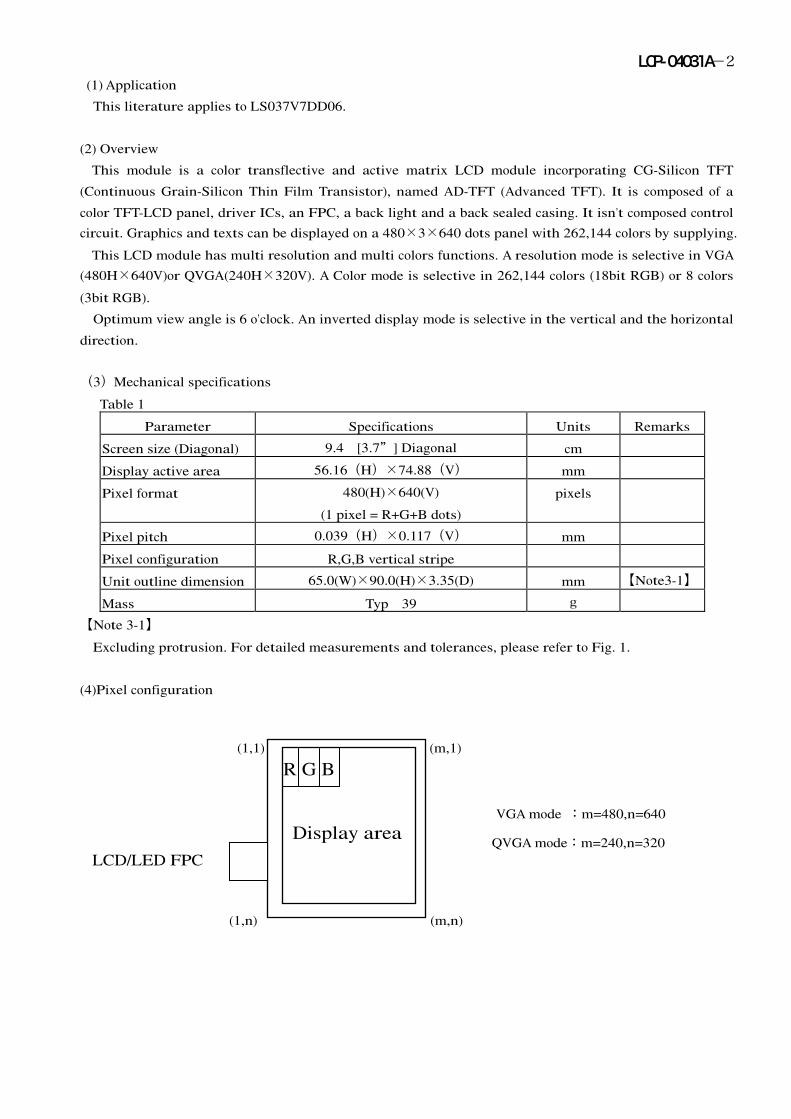
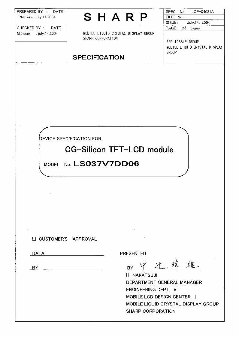
LCP-04031A-2 (1) Application
This literature applies to LS037V7DD06.
(2) Overview
This module is a color transflective and active matrix LCD module incorporating CG-Silicon TFT
(Continuous Grain-Silicon Thin Film Transistor), named AD-TFT (Advanced TFT). It is composed of a
color TFT-LCD panel, driver ICs, an FPC, a back light and a back sealed casing. It isn’t composed control
circuit. Graphics and texts can be displayed on a 480×3×640 dots panel with 262,144 colors by supplying.
This LCD module has multi resolution and multi colors functions. A resolution mode is selective in VGA
(480H×640V)or QVGA(240H×320V). A Color mode is selective in 262,144 colors (18bit RGB) or 8 colors
(3bit RGB).
Optimum view angle is 6 o’clock. An inverted display mode is selective in the vertical and the horizontal
direction.
(3)Mechanical specifications
Table 1
Parameter Specifications Units Remarks
Screen size (Diagonal) 9.4 [3.7” ] Diagonal cm
Display active area 56.16(H)×74.88(V) mm
Pixel format 480(H)×640(V)
(1 pixel = R+G+B dots)
pixels
Pixel pitch 0.039(H)×0.117(V) mm
Pixel configuration R,G,B vertical stripe
Unit outline dimension 65.0(W)×90.0(H)×3.35(D) mm 【Note3-1】
Mass Typ 39 g
【Note 3-1】
Excluding protrusion. For detailed measurements and tolerances, please refer to Fig. 1.
(4)Pixel configuration
QVGA mode:m=240,n=320
VGA mode :m=480,n=640
(m,n)
Display area
(m,1) (1,1)
(1,n)
R G B
LCD/LED FPC
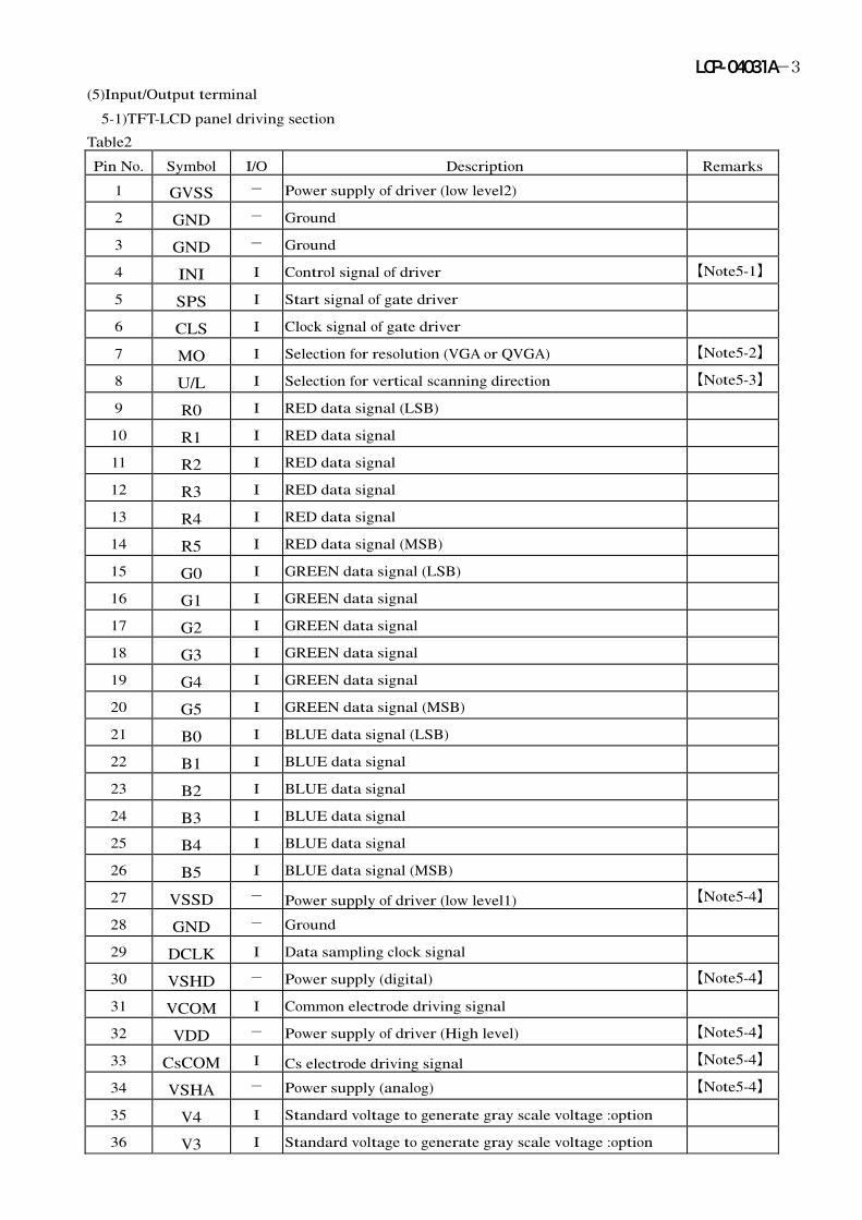
LCP-04031A-3 (5)Input/Output terminal
5-1)TFT-LCD panel driving section
Table2
Pin No. Symbol I/O Description Remarks
1 GVSS - Power supply of driver (low level2)
2 GND - Ground
3 GND - Ground
4 INI I Control signal of driver 【Note5-1】
5 SPS I Start signal of gate driver
6 CLS I Clock signal of gate driver
7 MO I Selection for resolution (VGA or QVGA) 【Note5-2】
8 U/L I Selection for vertical scanning direction 【Note5-3】
9 R0 I RED data signal (LSB)
10 R1 I RED data signal
11 R2 I RED data signal
12 R3 I RED data signal
13 R4 I RED data signal
14 R5 I RED data signal (MSB)
15 G0 I GREEN data signal (LSB)
16 G1 I GREEN data signal
17 G2 I GREEN data signal
18 G3 I GREEN data signal
19 G4 I GREEN data signal
20 G5 I GREEN data signal (MSB)
21 B0 I BLUE data signal (LSB)
22 B1 I BLUE data signal
23 B2 I BLUE data signal
24 B3 I BLUE data signal
25 B4 I BLUE data signal
26 B5 I BLUE data signal (MSB)
27 VSSD - Power supply of driver (low level1) 【Note5-4】
28 GND - Ground
29 DCLK I Data sampling clock signal
30 VSHD - Power supply (digital) 【Note5-4】
31 VCOM I Common electrode driving signal
32 VDD - Power supply of driver (High level) 【Note5-4】
33 CsCOM I Cs electrode driving signal 【Note5-4】
34 VSHA - Power supply (analog) 【Note5-4】
35 V4 I Standard voltage to generate gray scale voltage :option
36 V3 I Standard voltage to generate gray scale voltage :option
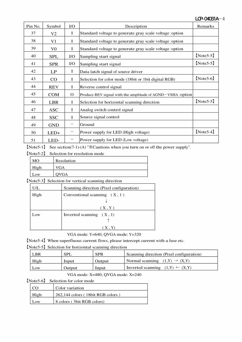
LCP-04031A-4 Pin No. Symbol I/O Description Remarks
37 V2 I Standard voltage to generate gray scale voltage :option
38 V1 I Standard voltage to generate gray scale voltage :option
39 V0 I Standard voltage to generate gray scale voltage :option
40 SPL I/O Sampling start signal 【Note5-5】
41 SPR I/O Sampling start signal 【Note5-5】
42 LP I Data latch signal of source driver
43 CO I Selection for color mode (18bit or 1bit digital RGB) 【Note5-6】
44 REV I Reverse control signal
45 COM O Produce REV signal with the amplitude of AGND-VSHA :option
46 LBR I Selection for horizontal scanning direction 【Note5-5】
47 ASC I Analog switch control signal
48 SSC I Source signal control
49 GND - Ground
50 LED+ - Power supply for LED (High voltage) 【Note5-4】
51 LED- - Power supply for LED (Low voltage)
【Note5-1】 See section(7-1)-(A) ”※Cautions when you turn on or off the power supply”.
【Note5-2】 Selection for resolution mode
MO Resolution
High VGA
Low QVGA
【Note5-3】Selection for vertical scanning direction
U/L Scanning direction (Pixel configuration)
High Conventional scanning ( X , 1 )
↓
( X , Y )
Low Inverted scanning ( X , 1)
↑
( X , Y)
VGA mode: Y=640, QVGA mode: Y=320
【Note5-4】When superfluous current flows, please intercept current with a fuse etc.
【Note5-5】Selection for horizontal scanning direction
LBR SPL SPR Scanning direction (Pixel configuration)
High Input Output Normal scanning (1,Y) → (X,Y)
Low Output Input Inverted scanning (1,Y) ← (X,Y)
VGA mode: X=480, QVGA mode: X=240
【Note5-6】 Selection for color mode
CO Color variation
High 262,144 colors ( 18bit RGB colors )
Low 8 colors ( 3bit RGB colors)
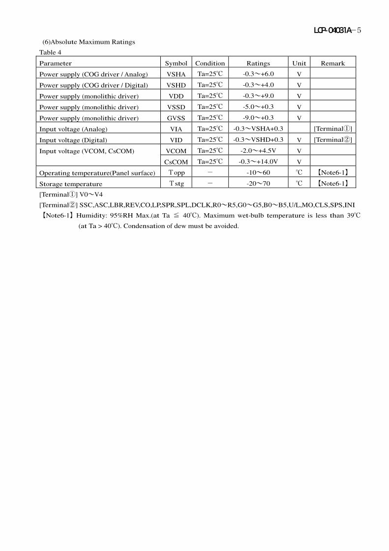
LCP-04031A-5 (6)Absolute Maximum Ratings
Table 4
Parameter Symbol Condition Ratings Unit Remark
Power supply (COG driver / Analog) VSHA Ta=25℃ -0.3~+6.0 V
Power supply (COG driver / Digital) VSHD Ta=25℃ -0.3~+4.0 V
Power supply (monolithic driver) VDD Ta=25℃ -0.3~+9.0 V
Power supply (monolithic driver) VSSD Ta=25℃ -5.0~+0.3 V
Power supply (monolithic driver) GVSS Ta=25℃ -9.0~+0.3 V
Input voltage (Analog) VIA Ta=25℃ -0.3~VSHA+0.3 [Terminal①]
Input voltage (Digital) VID Ta=25℃ -0.3~VSHD+0.3 V [Terminal②]
VCOM Ta=25℃ -2.0~+4.5V V Input voltage (VCOM, CsCOM)
CsCOM Ta=25℃ -0.3~+14.0V V
Operating temperature(Panel surface) Topp - -10~60 ℃ 【Note6-1】
Storage temperature Tstg - -20~70 ℃ 【Note6-1】
[Terminal①] V0~V4
[Terminal②] SSC,ASC,LBR,REV,CO,LP,SPR,SPL,DCLK,R0~R5,G0~G5,B0~B5,U/L,MO,CLS,SPS,INI
【Note6-1】Humidity: 95%RH Max.(at Ta ≦ 40℃). Maximum wet-bulb temperature is less than 39℃
(at Ta > 40℃). Condensation of dew must be avoided.
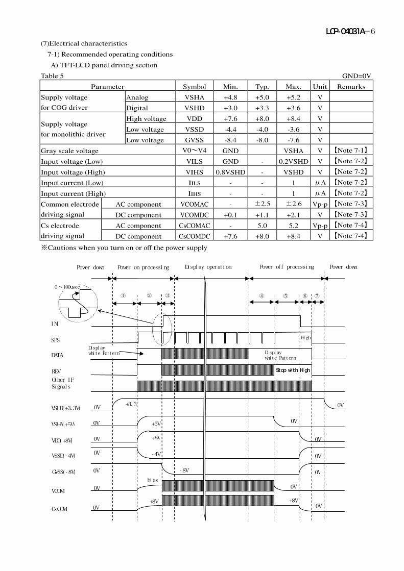
LCP-04031A-6 (7)Electrical characteristics
7-1) Recommended operating conditions
A) TFT-LCD panel driving section
Table 5 GND=0V
Parameter Symbol Min. Typ. Max. Unit Remarks
Analog VSHA +4.8 +5.0 +5.2 V Supply voltage
for COG driver Digital VSHD +3.0 +3.3 +3.6 V
High voltage VDD +7.6 +8.0 +8.4 V
Low voltage VSSD -4.4 -4.0 -3.6 V Supply voltage
for monolithic driver Low voltage GVSS -8.4 -8.0 -7.6 V
Gray scale voltage V0~V4 GND VSHA V 【Note 7-1】
Input voltage (Low) VILS GND - 0.2VSHD V 【Note 7-2】
Input voltage (High) VIHS 0.8VSHD - VSHD V 【Note 7-2】
Input current (Low) IILS - - 1 μA 【Note 7-2】
Input current (High) IIHS - - 1 μA 【Note 7-2】
AC component VCOMAC - ±2.5 ±2.6 Vp-p 【Note 7-3】 Common electrode
driving signal DC component VCOMDC +0.1 +1.1 +2.1 V 【Note 7-3】
AC component CsCOMAC - 5.0 5.2 Vp-p 【Note 7-4】 Cs electrode
driving signal DC component CsCOMDC +7.6 +8.0 +8.4 V 【Note 7-4】
※ Cautions when you turn on or off the power supply
INI
SPS
VDD( +8V)
VSSD( - 4V)
GVSS( - 8V)
VSHA( +5V)
VSHD( +3. 3V)
VCOM
CsCOM
Other IF Si gnal s
Di spl ay operat i on
REV
DATA
Power on processi ng Power of f processi ng Power down Power down
0V
0V
0V
0V
0V
0V
0V
+3. 3
+5V
+8V
- 4V
- 8Vbi as
+8V
0V
+8V 0V
Di spl ay whi t e Pat t ern
Stop wi th Hi gh
0V
0V
0V
0V
0V
Hi gh
Di spl ay whi t e Pat t ern
① ② ③ ④ ⑤ ⑥ ⑦
0~100usec
LCP-04031A-7 ①Stabilize VSHD(3.3V) within double vertical periods second.
②Supply SPS, DATA(White pattern), REV(with High), and other signals. Stabilize VSHA(+5V),
VDD(+8V), VSSD(-4V) within double vertical periods.
③INI signal and GVSS(–8V) are supplied. Stabilize GVSS(-8V) within single vertical period.
④White pattern is displayed during double or more vertical periods.
⑤REV signal is stopped with High level. VSHA(+5V) supply is stopped, which is stabilized within
double vertical periods.
⑥VDD(+8V),VSSD(-4V) and GVSS(-8V) supplys are stopped, which are stabilized within double vertical
periods.
⑦SPS,DATA,REV and other IF signals are stopped with Low level. Then VSHD(+3.3V) supply is stopped.
【Note 7-1】These are standard input voltages for gray scale. When VCOM is alternated polarity,
these voltage should be alternated polarity. V0(black) is different polarity alternating signal
of VCOM. V4(white) is the same polarity alternating signal of VCOM. Center voltage of each
standard input voltage shift positive way for LCD characteristics (V0→V1→V2→V3→V4 ).
This sift amount is adjusted so as to no flicker of each standard input voltage after
DC bias voltage of VCOM and V0 is adjusted.
【Note 7-2】SSC,ASC,LBR,REV,CO,LP,SPR,SPL,DCLK,U/L,MO,CLS,SPS,INI,R0~R5,G0~G5,B0~B5
terminals are applied.
【Note 7-3】VCOMAC should be alternated on VCOMDC every 1 horizontal period
and 1 vertical period. VCOMDC bias is adjusted so as to minimize flicker
or maximum contrast every each module . VCOM=VCOMAC+VCOMDC
【Note 7-4】CsCOMAC should be alternated on CsCOMDC every 1 horizontal period and 1 vertical period.
CsCOM’s phase is as same as VCOM’s. CsCOM=CsCOMAC+CsCOMDC
B) Back light driving section
Table 6 Ta=25℃
Parameter Symbol MIN TYP MAX Units Remarks terminal
LED voltage VL - 32.4 37.8 V 【Note 7-5】
LED current IL - 15.0 20.0 mA
Power consumption WL - 486 - mW 【Note 7-6】
【Note 7-5】VL(TYP) at IL=15mA. VL(MAX) at IL=20mA.
【Note 7-6】Calculated reference value(IL(TYP)×VL(TYP))
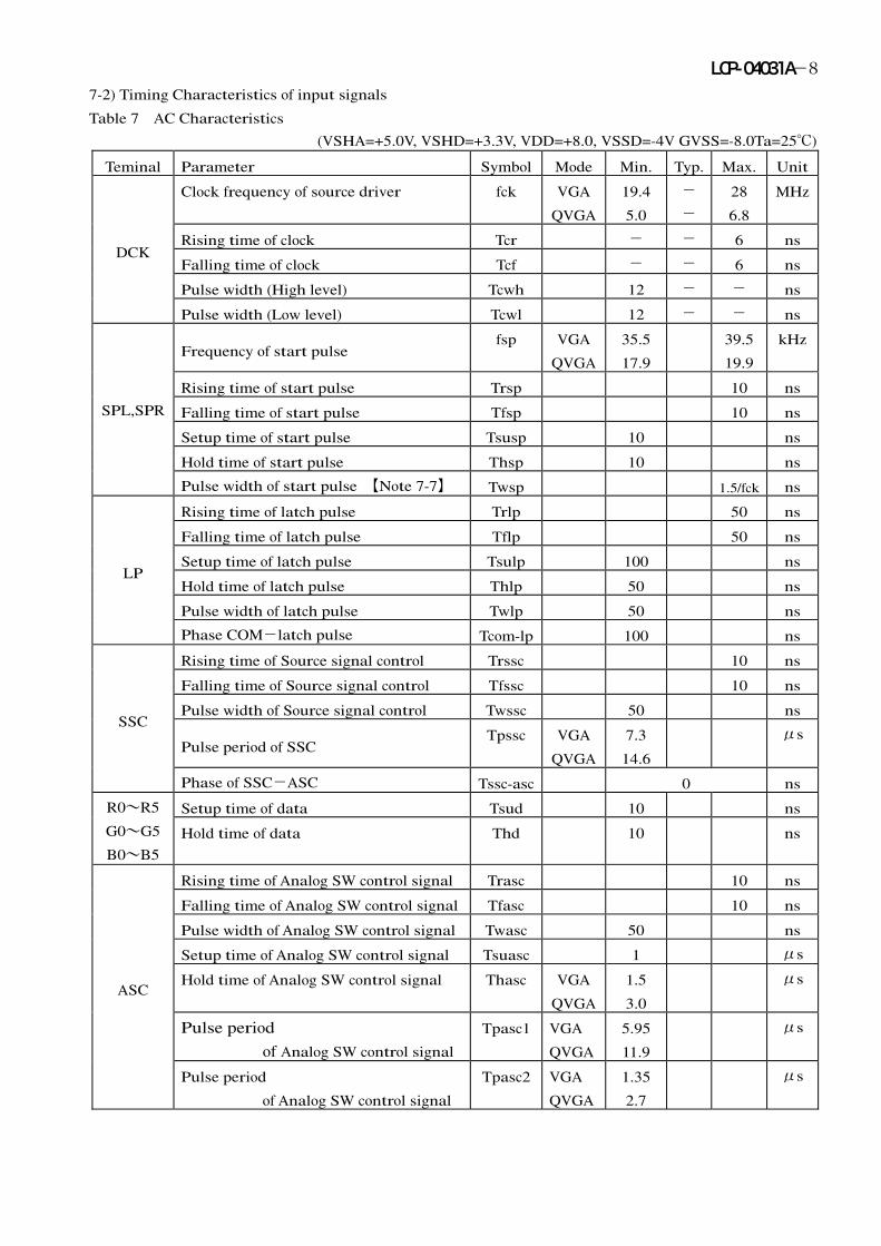
LCP-04031A-8 7-2) Timing Characteristics of input signals
Table 7 AC Characteristics
(VSHA=+5.0V, VSHD=+3.3V, VDD=+8.0, VSSD=-4V GVSS=-8.0Ta=25℃)
Teminal Parameter Symbol Mode Min. Typ. Max. Unit
Clock frequency of source driver fck VGA
QVGA
19.4
5.0
-
-
28
6.8
MHz
Rising time of clock Tcr - - 6 ns
Falling time of clock Tcf - - 6 ns
Pulse width (High level) Tcwh 12 - - ns
DCK
Pulse width (Low level) Tcwl 12 - - ns
Frequency of start pulse fsp VGA
QVGA
35.5
17.9
39.5
19.9
kHz
Rising time of start pulse Trsp 10 ns
Falling time of start pulse Tfsp 10 ns
Setup time of start pulse Tsusp 10 ns
Hold time of start pulse Thsp 10 ns
SPL,SPR
Pulse width of start pulse 【Note 7-7】 Twsp 1.5/fck ns
Rising time of latch pulse Trlp 50 ns
Falling time of latch pulse Tflp 50 ns
Setup time of latch pulse Tsulp 100 ns
Hold time of latch pulse Thlp 50 ns
Pulse width of latch pulse Twlp 50 ns
LP
Phase COM-latch pulse Tcom-lp 100 ns
Rising time of Source signal control Trssc 10 ns
Falling time of Source signal control Tfssc 10 ns
Pulse width of Source signal control Twssc 50 ns
Pulse period of SSC Tpssc VGA
QVGA
7.3
14.6
μs SSC
Phase of SSC-ASC Tssc-asc 0 ns
Setup time of data Tsud 10 ns R0~R5
G0~G5
B0~B5 Hold time of data Thd 10 ns
Rising time of Analog SW control signal Trasc 10 ns
Falling time of Analog SW control signal Tfasc 10 ns
Pulse width of Analog SW control signal Twasc 50 ns
Setup time of Analog SW control signal Tsuasc 1 μs
Hold time of Analog SW control signal Thasc VGA
QVGA
1.5
3.0
μs
Pulse period of Analog SW control signal
Tpasc1 VGA
QVGA
5.95
11.9
μs
ASC
Pulse period
of Analog SW control signal
Tpasc2 VGA
QVGA
1.35
2.7
μs
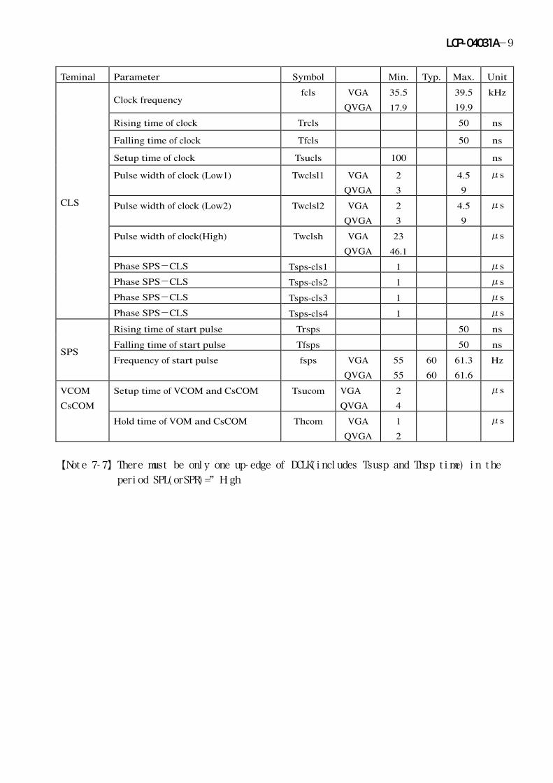
LCP-04031A-9 Teminal Parameter Symbol Min. Typ. Max. Unit
Clock frequency fcls VGA
QVGA
35.5
17.9
39.5
19.9
kHz
Rising time of clock Trcls 50 ns
Falling time of clock Tfcls 50 ns
Setup time of clock Tsucls 100 ns
Pulse width of clock (Low1) Twclsl1 VGA
QVGA
2
3
4.5
9
μs
Pulse width of clock (Low2) Twclsl2 VGA
QVGA
2
3
4.5
9
μs
Pulse width of clock(High) Twclsh VGA
QVGA
23
46.1
μs
Phase SPS-CLS Tsps-cls1 1 μs
Phase SPS-CLS Tsps-cls2 1 μs
Phase SPS-CLS Tsps-cls3 1 μs
CLS
Phase SPS-CLS Tsps-cls4 1 μs
Rising time of start pulse Trsps 50 ns
Falling time of start pulse Tfsps 50 ns SPS
Frequency of start pulse fsps VGA
QVGA
55
55
60
60
61.3
61.6
Hz
Setup time of VCOM and CsCOM Tsucom VGA
QVGA
2
4
μs VCOM
CsCOM
Hold time of VOM and CsCOM Thcom VGA
QVGA
1
2
μs
【Not e 7- 7】There must be onl y one up- edge of DCLK( i ncl udes Tsusp and Thsp t i me) i n t he
peri od SPL( orSPR) =” Hi gh
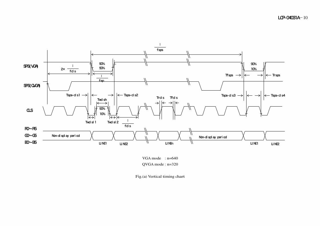
LCP-04031A-10
VGA mode : n=640
QVGA mode : n=320
Fig.(a) Vertical timing chart
SPS(QVGA)
CLS
LI NEn
LI NE1 LI NE2
R0~R5 G0~G5 B0~B5
SPS(VGA)
Non-di spl ay peri od
LI NE1 LI NE2
Non-di spl ay peri od
10% 90%
50% 90% 10%
Twcl sl 1 Twcl sl 2
Twcl sh Tsps-cl s1 Tsps-cl s2 Tsps-cl s3 Tsps-cl s4
90%
Tfsps Trsps
Trcl s Tfcl s
fsps 1
2× fcl s 1
fsp 1
fcl s 1
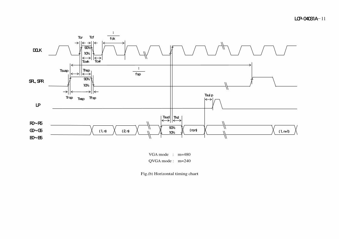
LCP-04031A-11
VGA mode : m=480
QVGA mode : m=240
Fig.(b) Horizontal timing chart
(1, n) (m, n)
SPL, SPR
(1, n+1)
DCLK
(2, n)
90% 10%
Tsud
90%
90% 10%
R0~R5 G0~G5 B0~B5
Thd
10%
Tcr Tcf
Tcwh Tcwl
Tsusp Thsp
Trsp Tfsp
LP
Tsul p
fsp 1
fck 1
Twsp
LCP-04031A-12
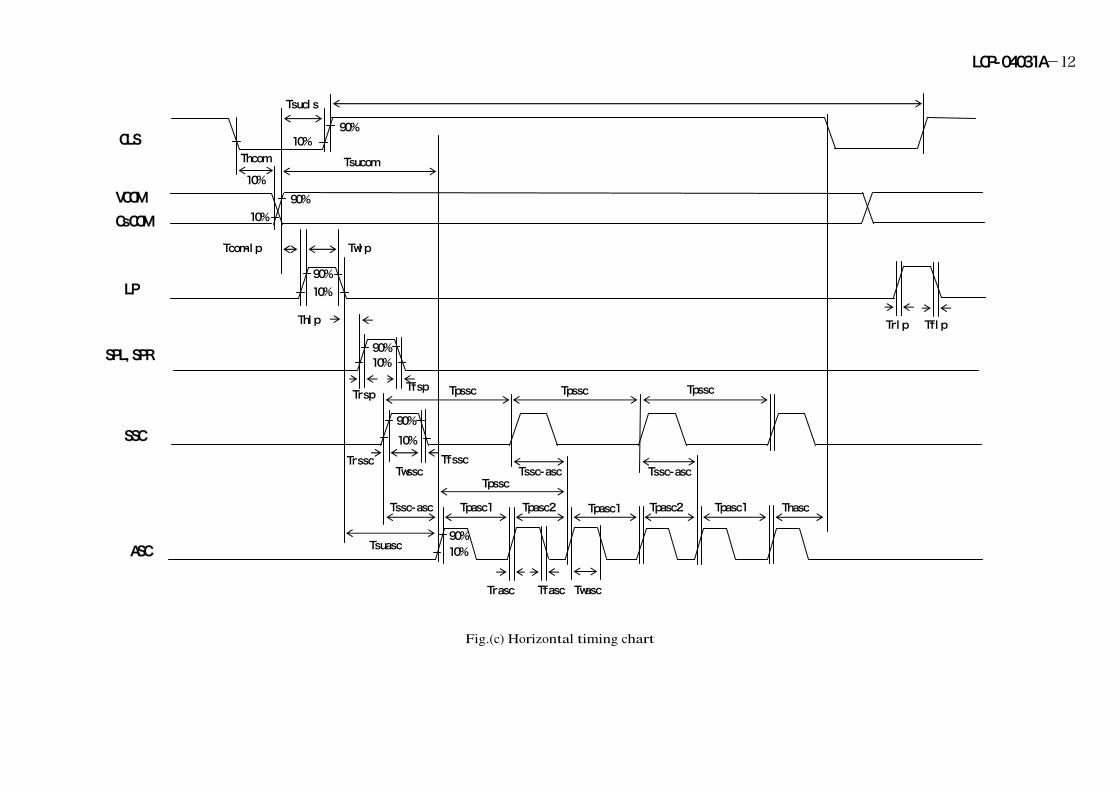
Fig.(c) Horizontal timing chart
CLS
VCOM CsCOM
LP
SPL, SPR
SSC
ASC
90% 10%
10% 90%
90% 10%
10% 90%
10% 90%
10% 90%
Tpasc1 Tpasc1 Tpasc1 Tpasc2 Tpasc2
Tsuasc
Trasc Tfasc
Trl p Tfl p
Thasc
Trssc Tfssc
Tpssc Tpssc Tpssc
Tssc-asc
Tssc-asc
10%
Twl p
Thcom
Tsucl s
Tsucom
Tcom-l p
Thl p
Trsp Tfsp
Twssc
Twasc
Tssc-ascTpssc
LCP-04031A-13
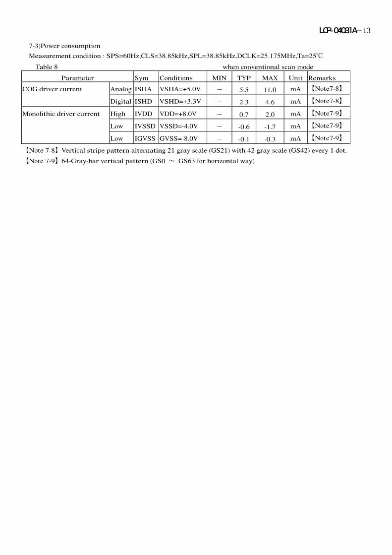
7-3)Power consumption
Measurement condition : SPS=60Hz,CLS=38.85kHz,SPL=38.85kHz,DCLK=25.175MHz,Ta=25℃
Table 8 when conventional scan mode
Parameter Sym Conditions MIN TYP MAX Unit Remarks
Analog ISHA VSHA=+5.0V - 5.5 11.0 mA 【Note7-8】 COG driver current
Digital ISHD VSHD=+3.3V - 2.3 4.6 mA 【Note7-8】
High IVDD VDD=+8.0V - 0.7 2.0 mA 【Note7-9】
Low IVSSD VSSD=-4.0V - -0.6 -1.7 mA 【Note7-9】
Monolithic driver current
Low IGVSS GVSS=-8.0V - -0.1 -0.3 mA 【Note7-9】
【Note 7-8】Vertical stripe pattern alternating 21 gray scale (GS21) with 42 gray scale (GS42) every 1 dot.
【Note 7-9】64-Gray-bar vertical pattern (GS0 ~ GS63 for horizontal way)
LCP-04031A-14
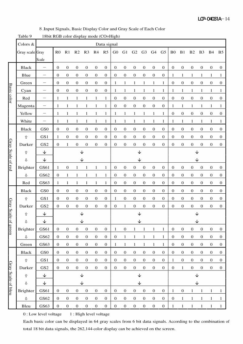
8.Input Signals, Basic Display Color and Gray Scale of Each Color
Table 9 18bit RGB color display mode (CO=High)
Colors & Data signal
Gray scale Gray
Scale
R0 R1 R2 R3 R4 R5 G0 G1 G2 G3 G4 G5 B0 B1 B2 B3 B4 B5
Black - 0 0 0 0 0 0 0 0 0 0 0 0 0 0 0 0 0 0
Blue - 0 0 0 0 0 0 0 0 0 0 0 0 1 1 1 1 1 1
Green - 0 0 0 0 0 0 1 1 1 1 1 1 0 0 0 0 0 0
Cyan - 0 0 0 0 0 0 1 1 1 1 1 1 1 1 1 1 1 1
Red - 1 1 1 1 1 1 0 0 0 0 0 0 0 0 0 0 0 0
Magenta - 1 1 1 1 1 1 0 0 0 0 0 0 1 1 1 1 1 1
Yellow - 1 1 1 1 1 1 1 1 1 1 1 1 0 0 0 0 0 0
Basic color
White - 1 1 1 1 1 1 1 1 1 1 1 1 1 1 1 1 1 1
Black GS0 0 0 0 0 0 0 0 0 0 0 0 0 0 0 0 0 0 0
× GS1 1 0 0 0 0 0 0 0 0 0 0 0 0 0 0 0 0 0
Darker GS2 0 1 0 0 0 0 0 0 0 0 0 0 0 0 0 0 0 0
× È È È È
Ø È È È È
Brighter GS61 1 0 1 1 1 1 0 0 0 0 0 0 0 0 0 0 0 0
Ø GS62 0 1 1 1 1 1 0 0 0 0 0 0 0 0 0 0 0 0
Gray S
cale of red
Red GS63 1 1 1 1 1 1 0 0 0 0 0 0 0 0 0 0 0 0
Black GS0 0 0 0 0 0 0 0 0 0 0 0 0 0 0 0 0 0 0
× GS1 0 0 0 0 0 0 1 0 0 0 0 0 0 0 0 0 0 0
Darker GS2 0 0 0 0 0 0 0 1 0 0 0 0 0 0 0 0 0 0
× È È È È
Ø È È È È
Brighter GS61 0 0 0 0 0 0 1 0 1 1 1 1 0 0 0 0 0 0
Ø GS62 0 0 0 0 0 0 0 1 1 1 1 1 0 0 0 0 0 0 G
ray Scale of green
Green GS63 0 0 0 0 0 0 1 1 1 1 1 1 0 0 0 0 0 0
Black GS0 0 0 0 0 0 0 0 0 0 0 0 0 0 0 0 0 0 0
× GS1 0 0 0 0 0 0 0 0 0 0 0 0 1 0 0 0 0 0
Darker GS2 0 0 0 0 0 0 0 0 0 0 0 0 0 1 0 0 0 0
× È È È È
Ø È È È È
Brighter GS61 0 0 0 0 0 0 0 0 0 0 0 0 1 0 1 1 1 1
Ø GS62 0 0 0 0 0 0 0 0 0 0 0 0 0 1 1 1 1 1
Gray S
cale of bleu
Bleu GS63 0 0 0 0 0 0 0 0 0 0 0 0 1 1 1 1 1 1
0 : Low level voltage 1 : High level voltage
Each basic color can be displayed in 64 gray scales from 6 bit data signals. According to the combination of
total 18 bit data signals, the 262,144-color display can be achieved on the screen.
LCP-04031A-15
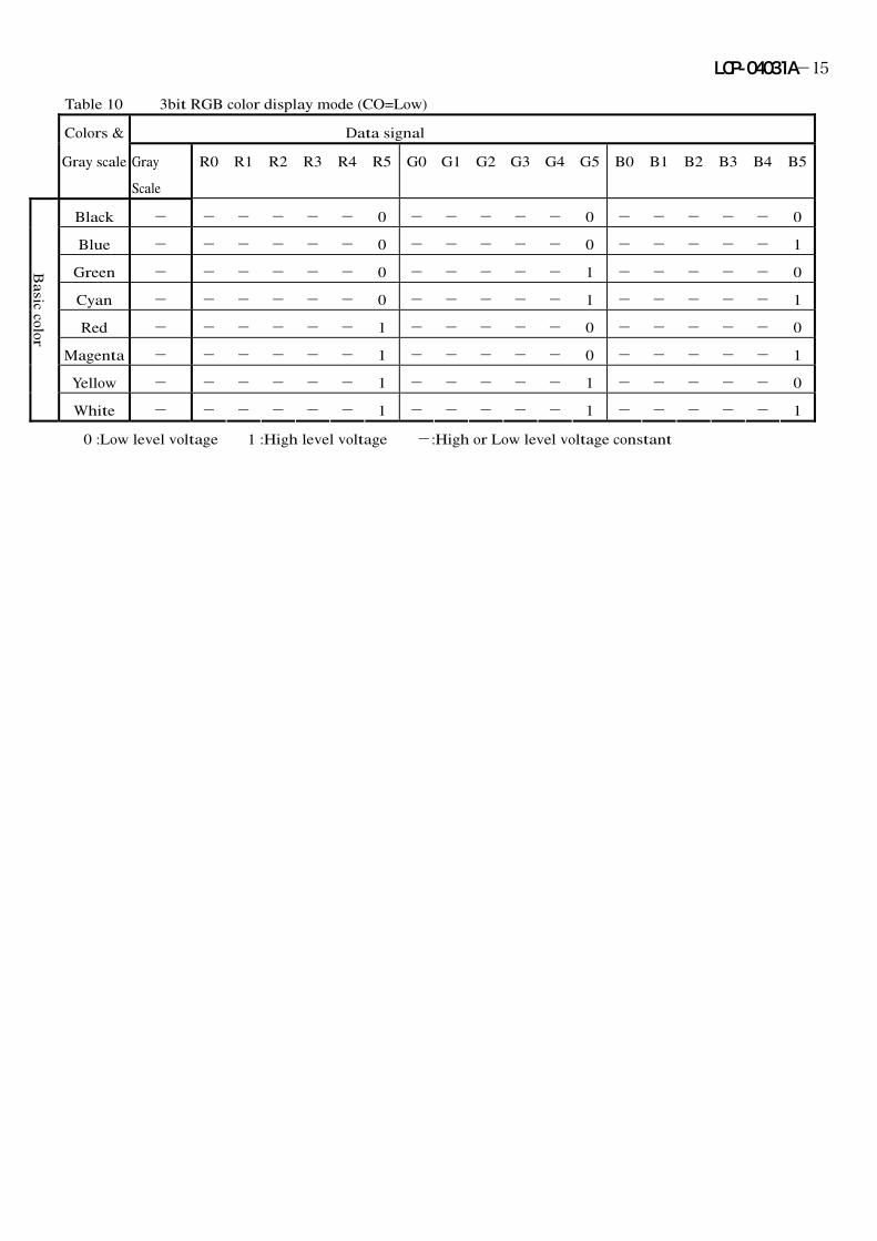
Table 10 3bit RGB color display mode (CO=Low)
Colors & Data signal
Gray scale Gray
Scale
R0 R1 R2 R3 R4 R5 G0 G1 G2 G3 G4 G5 B0 B1 B2 B3 B4 B5
Black - - - - - - 0 - - - - - 0 - - - - - 0
Blue - - - - - - 0 - - - - - 0 - - - - - 1
Green - - - - - - 0 - - - - - 1 - - - - - 0
Cyan - - - - - - 0 - - - - - 1 - - - - - 1
Red - - - - - - 1 - - - - - 0 - - - - - 0
Magenta - - - - - - 1 - - - - - 0 - - - - - 1
Yellow - - - - - - 1 - - - - - 1 - - - - - 0
Basic color
White - - - - - - 1 - - - - - 1 - - - - - 1
0 :Low level voltage 1 :High level voltage -:High or Low level voltage constant
LCP-04031A-16
(9)Optical characteristics 9-1) Not driving the Back light condition Table 11 Ta=25qC
Parameter Symbol Condition Min Typ Max Unit Remarks
T21,22 20 30 - degree [Note 9-1,2]
T11 CRt2 20 30 - degree
Viewing angle Range
T12 20 30 - degree
Contrast ratio CRmax T =0q 3 5 - [Note 9-2,4]
Response Rise W r - 30 60 ms [Note 9-3]
time Fall W d - 50 100 ms
White chromaticity x 0.24 0.29 0.34 [Note 9-4]
y
T =0q
0.28 0.33 0.38
Reflection ratio R T =0q 4 6 - % [Note 9-5]
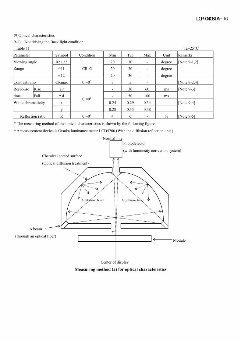
* The measuring method of the optical characteristics is shown by the following figure.
* A measurement device is Otsuka luminance meter LCD5200.(With the diffusion reflection unit.) Center of display
Measuring method (a) for optical characteristics
Photodetector (with luminosity correction system)
Module
Chemical coated surface
(Optical diffusion treatment)
A diffusion beam A diffusion beam
Normal line
A beam
(through an optical fiber)
LCP-04031A-17 9-2) Driving the Back light condition Table 12 Ta=25qC
Parameter Symbol Condition Min Typ Max Unit Remarks
T21,22 30 40 - degree [Note 9-1,2,6]
T11 CRt2 30 40 - degree
Viewing angle range
T12 30 40 - degree
Contrast ratio Crmax T = 0q 70 100 - [Note 9-2]
Rise W r - 30 60 ms [Note 9-3] Response time Fall W d - 50 100 ms
White chromaticity x 0.23 0.28 0.33
y
0.25 0.30 0.35
Brightness Y T = 0q 85 100 - (cd/m2) IL=15mA
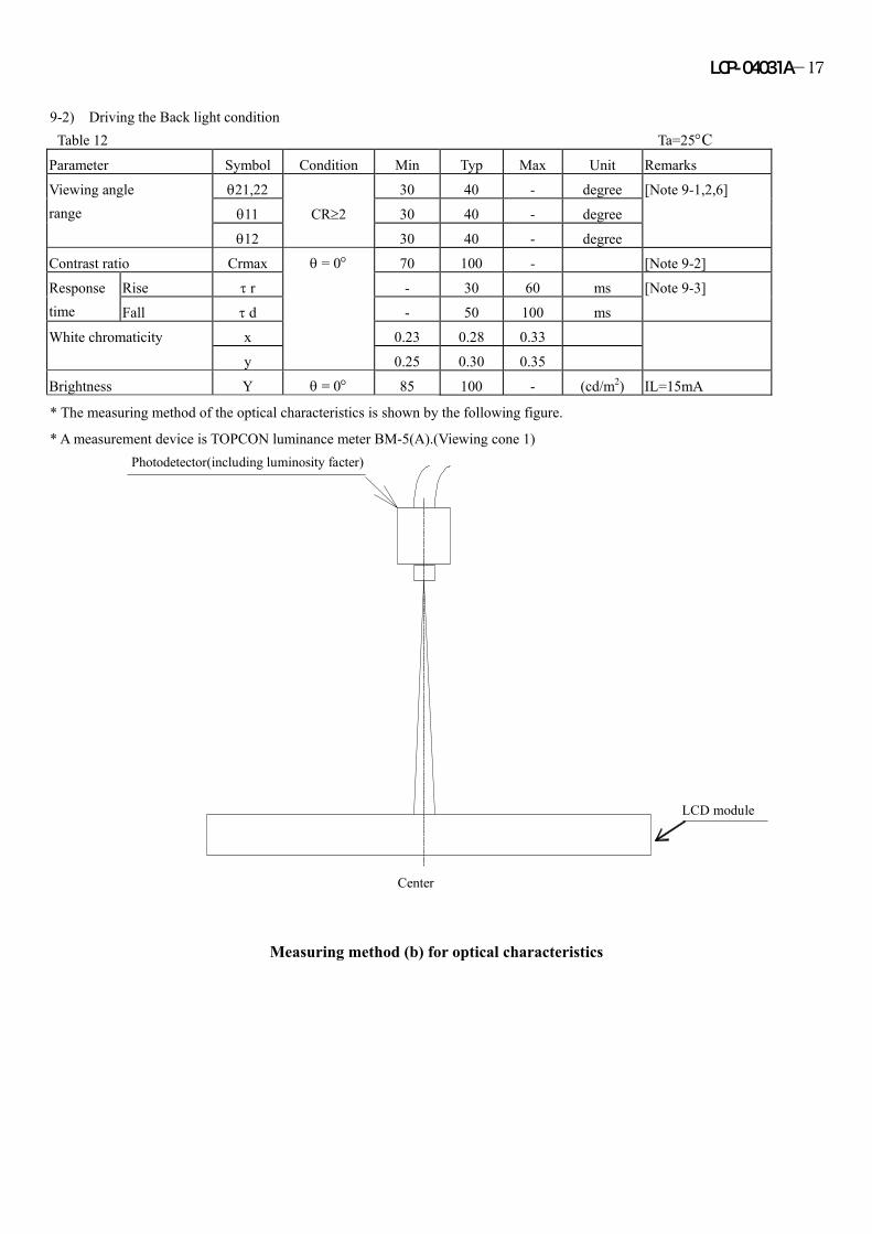
* The measuring method of the optical characteristics is shown by the following figure.
* A measurement device is TOPCON luminance meter BM-5(A).(Viewing cone 1)
Measuring method (b) for optical characteristics
Photodetector(including luminosity facter)
Center
LCD module
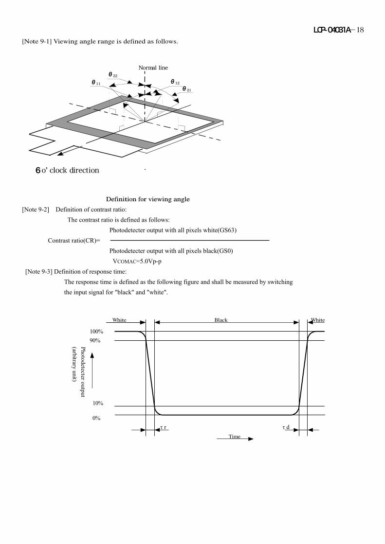
LCP-04031A-18 [Note 9-1] Viewing angle range is defined as follows.
6o’ clock direction
θ12θ22
θ11 θ21
Normal line
Definition for viewing angle
[Note 9-2] Definition of contrast ratio: The contrast ratio is defined as follows: Photodetecter output with all pixels white(GS63) Contrast ratio(CR)= Photodetecter output with all pixels black(GS0) VCOMAC=5.0Vp-p [Note 9-3] Definition of response time: The response time is defined as the following figure and shall be measured by switching the input signal for "black" and "white".
0%
10%
90%100%
Black WhiteWhite
W d W rTime
Photodetecter output(arbitrary unit)
LCP-04031A-19 [Note 9-4] A measurement device is Minolta CM-2002. [Note 9-5] Definition of reflection ratio Reflection ratio = [Note 9-6] A measurement device is ELDIM EZContrast (10) Display quality
The display quality of the color TFT-LCD module shall be in compliance with
the Incoming Inspection Standards for TFT-LCD..
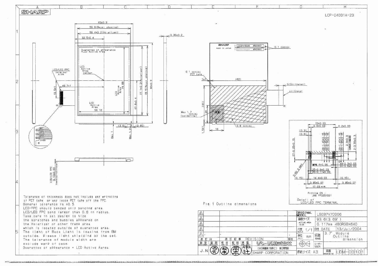
(11)Mechanical characteristics
11-1) External appearance
See Fig. 1
11-2) FPC (for LCD panel) characteristics
(1)Specific connector
LCD-FPC : JAE FF0251SS1 (Bottom contact only)
(2) Bending endurance
No line of the FPC is broken for the bending test (Bending radius=0.6mm and
angle=90°) in 30 cycles.
Light detected level of the reflection by the LCD module Light detected level of the reflection by the standard white board
LCP-04031A-20 (12)Handling Precautions
12-1) Insertion and taking out of FPCs
Be sure insert and take out of the FPC into the connector of the set after turning off the power
supply on the set side.
12-2) Handling of FPCs
The FPC for LCD panel shall be bent only slit portion. The bending slit shall be bent uniformly
on the whole slit portion with bending radius larger than 0.6mm ,and only inner side (back side
of the module). Don’t bend it outer side (display surface side).
Don’t give the FPCs too large force, for example, hanging the module with holding FPC.
12-3) Installation of the module
On mounting the module, be sure to fix the module on the same plane. Taking care not to warp or
twist the module.
12-4)Precaution when mounting
(1) If water droplets and oil attaches to it for a long time, discoloration and staining occurs. Wipe them off
immediately.
(2) Glass is used for the TFT-LCD panel. If it is dropped or bumped against a hard object, it may be broken.
Handle it with sufficient care.
(3)As the CMOS IC is used in this module, pay attention to static electricity when handling it. Take a
measure for grounding on the human body.
12-5)Others
(1) The liquid-crystal is deteriorated by ultraviolet rays. Do not leave it in direct sunlight and strong
ultraviolet rays for many hours.
(2) If it is kept at a temperature below the rated storage temperature, it becomes coagulated and the panel
may be broken. Also, if it is kept at a temperature above the rated storage temperature, it becomes
isotropic liquid and does not return to its original state. Therefore, it is desirable to keep it at room
temperature as much as possible.
(3) If the LCD breaks, don’t put internal liquid crystal into the mouth. When the liquid crystal sticks to the
hands, feet and clothes, wash it out immediately.
(4) Wipe off water drop or finger grease immediately. Long contact with water may cause discoloration or
spots.
(5) Observe general precautions for all electronic components.
(6) VCOM must be adjusted on condition of your final product. No adjustment causes the deterioration for
display quality.
(7) Static image should not be displayed more than 5 minutes in order to prevent from occurrence of
residual image.
LCP-04031A-21
(13)Reliability Test Conditions for TFT-LCD Module
Table 14
No. Test items Test conditions
1 High temperature storage
test
Ta=+70℃ 240h
2 Low temperature storage test Ta=-20℃ 240h
3 High temperature and high
humidity operating test
Tp=+40℃ , 95%RH 240h
(But no condensation of dew)
4 High temperature operating
test
Tp=+60℃ 240h
5 Low temperature operating
test
Tp=-10℃ 240h
6 Electro static discharge test ±200V・200pF(0Ω) 1 time for each terminals
7 Shock tset 980 m/s2, 6 ms
±X,±Y,±Z 3 times for each direction
(JIS C0041, A-7 Condition C)
8 Vibration test Frequency range: 10Hz~55Hz
Stroke: 1.5 mm Sweep: 10Hz~55Hz
X,Y,Z 2 hours for each direction (total 6 hours)
(JIS C0040,A-10 Condition A)
9 Heat shock test Ta=-20℃~+70℃ / 5 cycles
(1h) (1h)
LCP-04031A-22 【Note】Ta = Ambient temperature, Tp = Panel temperature
【Check items】
In the standard condition, there shall be no practical problems that may
affect the display function.
(14) Others
14-1)Indication of lot number
The lot number is shown on a label. Attached location is shown in Fig.1 (Outline Dimensions).
Indicated contents of the label
LS037V7DD06 ○○○○○○○○
model No. lot No.
14-2) Used Regulation of Chemical Substances Breaking Ozone Stratum
Substances with the object of regulating : CFCS, Carbon tetrachloride, Halon
1,1,1-Trichloro ethane (Methyl chloroform)
(a) This LCD module, Constructed part and Parts don’t contain the above substances.
(b) This LCD module, Constructed part and Parts don’t contain the above substances in processes of
manufacture.
14-3) If some problems arise about mentioned items in this document and other items, the user of
the TFT-LCD module and Sharp will cooperate and make efforts to solve the problems with mutual
respect and good will.
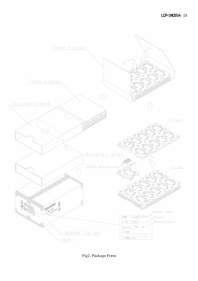
(15)Forwarding form (see Fig.2 Package Form)
a) Piling number of cartons : MAX 8
b) Package quality in one cartons : 100pcs
c) Carton size : 575mm × 360mm × 225mm
d) Total mass of 1 carton filled with full modules : 7900g
Conditions for storage.
Environment
(1)Temperature : 0~40℃
(2)Humidity : 60%RH or less (at 40℃)
No dew condensation at low temperature and high humidity.
(3)Atmosphere : Harmful gas, such as acid or alkali which bites electronic
components and/or wires, must not be detected.
(4)Period : about 3 months
(5)Opening of the package : In order to prevent the LCD module from breakdown by
electrostatic charges, please control the room humidity
over 50%RH and open the package taking sufficient
countermeasures against electrostatic charges, such as
earth, etc.
LCP-04031A-24
Fig2. Package Form