Embed Size (px)
Citation preview
NYQUIST MODULATION vs OFDM FOR FIBER-OPTIC
COMMUNICATIONS
A Degree Thesis
Submitted to the Faculty of the
Escola Tècnica d'Enginyeria de Telecomunicació de
Barcelona
Universitat Politècnica de Catalunya
by
Carles Escuder Folch
In partial fulfilment
of the requirements for the degree in
SCIENCE AND TELECOMUNICATION TECHNOLOGIES
ENGINEERING
Advisor: Joan M. Gené Bernaus
Barcelona, June 2016
1
Abstract
In nowadays society, the need of fast, reliable communications is growing faster
and faster each day. For this reason, there is the need of improving the current
communications systems in terms of speed (faster data transmission) and spectral
efficiency.
This thesis focus on the study of the Nyquist modulation. This modulation is based
on the use of Nyquist pulses conveniently allocated in time in order to make them
orthogonal. Due to this fact, in the frequency domain, these pulses are perfectly situated in
a finite frequency band. In other words, Nyquist modulation is an Orthogonal Time Division
Multiplexing (OTDM) in which the use of Nyquist pulses guarantee that they can perfectly
occupy a limited bandwidth in the frequency domain.
The main objective of this thesis is to get results for both an intensity Nyquist
modulation and QAM Nyquist modulation and make comparisons between them and with
a simple QAM modulation.
2
Resum
A la societat actual, la necessitat de comunicacions ràpides i fiables esta creixent
molt ràpidament. Per aquesta raó, existeix la necessitat de millorar les comunicacions
actuals en termes de velocitat i eficiència espectral.
Aquesta tesis es basa en l’estudi de la modulació de Nyquist. Aquesta modulació
consisteix en la utilització de polsos de Nyquist convenientment situats en el temps amb
l’objectiu de fer que siguin ortogonals entre ells. Al aconseguir col·locar els polsos
d’aquesta manera, aconseguim que aquests estiguin perfectament distribuïts ocupant una
banda de freqüència limitada. En altres paraules, La modulació de Nyquist és una OTDM
( Orthogonal Time DIvisión Multiplexing) on la utilització de polsos de Nyquist garanteix
que puguin distribuir-se perfectament en un ample de banda limitat.
L’objectiu principal d’aquesta tesis és aconseguir resultats per una modulació
d’intensitat utilitzant Nyquist i per una modulació QAM utilitzant Nyquist i poder comparar-
les entre elles i amb una modulació QAM simple.
3
Resumen
En la Sociedad actual, la necesidad de comunicaciones rápidas y fiables está
creciendo muy rápidamente. Por esta razón, existe la necesidad de mejorar las
comunicaciones actuales en términos de velocidad y eficiencia espectral.
Esta tesis se basa en el estudio de la modulación de Nyquist. Esta modulación
consiste en el estudio de pulsos de Nyquist convenientemente separados en el tiempo con
el objetivo de hacer que sean ortogonales entre ellos. Al conseguir colocar los pulsos de
esta manera, conseguimos que en el dominio frecuencial estos estén perfectamente
distribuidos ocupando una banda frecuencial limitada. En otras palabras, la modulación de
Nyquist es una OTDM (Orthogonal TIme DIvisión Multiplexing) donde la utilización de
pulsos de Nyquist consigue que puedan distribuirse perfectamente en un ancho de banda
limitado.
El objetivo principal de esta tesis es conseguir resultados para una modulación de
intensidad Nyquist y una modulación QAM utilizando Nyquist y poder compararlos entre si
y con una modulación QAM simple.

4
Dedicated to all my dear ones,
thank you for encouraging me and supporting my decisions throughout all these years.

5
Acknowledgements
I would like to thank Joan M. Gené Bernaus, my project supervisor. Giving me constant feedback during the whole project and planning weekly meetings allowed me to be confident about the work I was doing. In addition, he was really helpful during all the thesis and always had supportive and reassuring words.

6
Revision history and approval record
Revision Date Purpose
0 16/05/2016 Document creation
1 17/06/2016 Document revision
2 23/06/2016 Document revision
DOCUMENT DISTRIBUTION LIST
Name e-mail
Carles Escuder Folch [email protected]
Joan M. Gené [email protected]
Written by: Reviewed and approved by:
Date 16/05/2016 Date dd/mm/yyyy
Name Carles Escuder Name Joan M. Gené Bernaus
Position Project Author Position Project Supervisor
7
Table of contents
Abstract ................................................................................................................................. 1
Resum................................................................................................................................... 2
Resumen............................................................................................................................... 3
Acknowledgements .............................................................................................................. 5
Revision history and approval record ................................................................................... 6
Table of contents .................................................................................................................. 7
List of Figures ....................................................................................................................... 9
List of Tables: ..................................................................................................................... 11
1. Introduction.................................................................................................................. 12
1.1. Thesis Context ..................................................................................................... 12
1.2. State of the art...................................................................................................... 12
1.3. Objectives ............................................................................................................ 12
1.4. Work plan ............................................................................................................. 12
2. State of the art of the technology used or applied in this thesis:................................ 14
2.1. OFDM (Orthogonal Frequency Division Multiplexing)......................................... 14
2.1.1. Concept and Definition ................................................................................. 14
2.2. Nyquist Modulation .............................................................................................. 14
2.2.1. Definition and motivation .............................................................................. 14
2.2.2. Formal presentation...................................................................................... 15
2.2.3. Transmitter structure .................................................................................... 18
2.2.4. Receiver structure ........................................................................................ 18
2.2.5. Similarity with OFDM .................................................................................... 19
2.3. Nyquist Multiplexing ............................................................................................. 20
2.3.1. Concept......................................................................................................... 20
2.3.2. Transmitter.................................................................................................... 21
2.3.3. Receiver ........................................................................................................ 21
3. Methodology / project development: ........................................................................... 22
3.1. Introduction .......................................................................................................... 22
3.2. Nyquist Modulation .............................................................................................. 22
3.2.1. Transmitter.................................................................................................... 22
3.2.2. Receiver ........................................................................................................ 24
8
3.2.3. Roll-Off effect ................................................................................................ 25
3.3. QAM using Nyquist modulation ........................................................................... 27
3.4. Interfering Schematics ......................................................................................... 30
4. Results......................................................................................................................... 31
4.1. Intensity Modulation ............................................................................................. 31
4.2. QAM Nyquist modulation ..................................................................................... 32
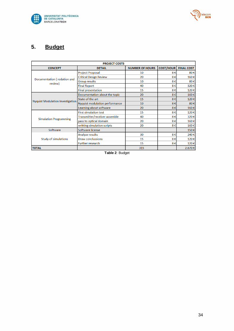
5. Budget ......................................................................................................................... 34
6. Conclusions and future development: ........................................................................ 35
Bibliography: ....................................................................................................................... 37
7. Appendices.................................................................................................................. 38
7.1. Rest of Simulations performed during the project development ......................... 38
7.1.1. QAM crosstalk comparison .......................................................................... 38
7.1.2. 64QAM crosstalk .......................................................................................... 38
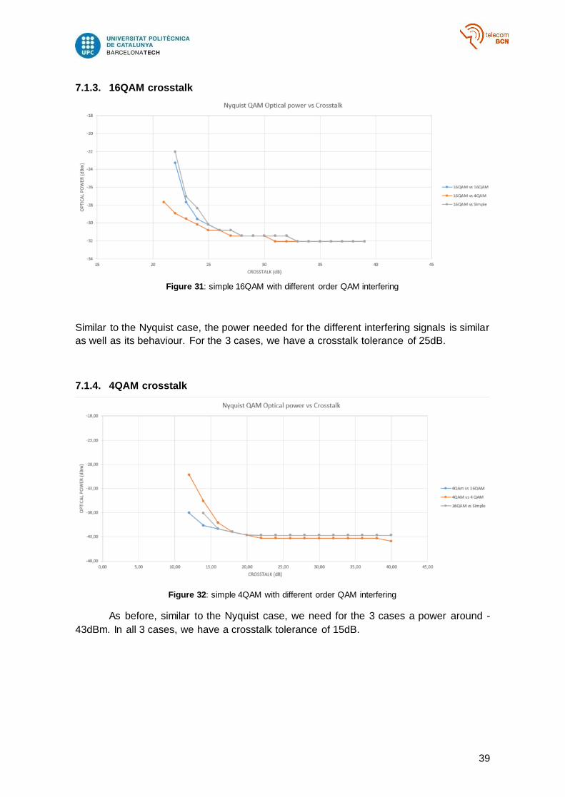
7.1.3. 16QAM crosstalk .......................................................................................... 39
7.1.4. 4QAM crosstalk ............................................................................................ 39
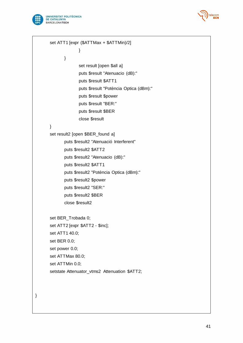
7.2. Simulation scripts ................................................................................................. 40
7.2.1. Crosstalk simulation script............................................................................ 40
7.3. Raised cosine Filter ............................................................................................. 42
7.4. QAM modulation .................................................................................................. 43
7.4.1. QAM Transmitter .......................................................................................... 43
7.4.2. QAM Receiver .............................................................................................. 44
7.4.3. Formal Presentation ..................................................................................... 45
7.4.4. Simple QAM schematic ................................................................................ 46
Glossary .............................................................................................................................. 49
9
List of Figures
Figure 1: OFDM concept ................................................................................................... 14
Figure 2: OFDM secondary lobes expansion.................................................................... 14
Figure 3: Nyquist modulation time domain ........................................................................ 16
Figure 4: Nyquist modulation frequency domain............................................................... 17
Figure 5: Nyquist modulation Transmitter scheme ........................................................... 18
Figure 6: Nyquist modulation receiver scheme ................................................................. 19
Figure 7: Comparison between Nyquist modulation and OFDM ...................................... 20
Figure 8: Nyquist multiplexing frequency domain ............................................................. 20
Figure 9: Nyquist Multiplexing transmitter scheme ........................................................... 21
Figure 10 : Nyquist Multiplexing receiver scheme ............................................................ 21
Figure 11: Nyquist modulation schematic ......................................................................... 22
Figure 12: Electric Nyquist modulation. 4 channels overlapped ....................................... 23
Figure 13: Electric Nyquist modulation. 4 channels overlapped zoom in ......................... 24
Figure 14: Electric Nyquist modulation receiver clock signal............................................ 25
Figure 15: comparison between transmitted and received signal eye diagram ............... 25
Figure 16: Exemplification of the Roll-off effect ................................................................ 26
Figure 17: Exemplification of the Roll-off effect when affecting bandwidth ...................... 26
Figure 18: QAM using Nyquist modulation schematic ...................................................... 27
Figure 19: QAM using Nyquist modulation 4 overlapped channels.................................. 28
Figure 20: QAM using Nyquist modulation 4 overlapped channels zoom in .................... 28
Figure 21: QAM using Nyquist modulation. Eye diagram of the 4 channels .................... 29
Figure 22: QAM using Nyquist modulation. Transmitted and received inphase and
quadrature eye diagram ..................................................................................................... 29
Figure 23: Optical Nyquist modulation interfering schematic ........................................... 30
Figure 24: Optical power vs crosstalk using Intensity modulation with different roll-off
effects ................................................................................................................................. 31
Figure 25: Optical power vs crosstalk using Intensity modulation different subcarriers .. 32
Figure 26: QAM vs Nyquist QAM comparison .................................................................. 32
Figure 27: Nyquist 16QAM with different QAM order interfering ...................................... 33
Figure 28: Nyquist 4QAM with different QAM order interfering ........................................ 33
Figure 29: simple QAM crosstalk comparison ................................................................. 38
Figure 30: simple 64QAM with different order QAM interfering ........................................ 38
Figure 31: simple 16QAM with different order QAM interfering ........................................ 39
10
Figure 32: simple 4QAM with different order QAM interfering .......................................... 39
Figure 33: raised-cosine filter ............................................................................................ 42
Figure 34: raised cosine impulse response....................................................................... 43
Figure 35: QAM transmitter ............................................................................................... 43
Figure 36: M transmitter in the Schematic ........................................................................ 44
Figure 37: QAM Receiver .................................................................................................. 44
Figure 38: QAM Receiver in Schematic ............................................................................ 45
Figure 39: QAM transmitter scheme ................................................................................. 45
Figure 40: QAM receiver scheme...................................................................................... 46
Figure 41: QAM schematic ................................................................................................ 46
Figure 42: QAM transmitted and received inphase and quadrature signals .................... 47
Figure 43: QAM transmitted and received inphase and quadrature eye diagram ........... 48
11
List of Tables:
Table 1: Gantt Diagram ...................................................................................................... 13
Table 2: Budget .................................................................................................................. 34
Table 3: Crosstalk results with different QAM interfering .................................................. 35
12
1. Introduction
1.1. Thesis Context
The thesis is inside the research work about modulations that is taking place at the
“Departament de Teoria del Senyal i Comunicacions (TSC)”, more precisely, inside the
“Grup de Comunicacions Òptiques (GCO)” which expert on the topic is the supervisor of
this thesis, Joan M. Gené Bernaus. The main objective of this thesis is to follow previously
done papers on Nyquist modulation by peers Jonathan Rodríguez Casal and Marc Jubany.
One of the optical communications advantages is its huge bandwidth, allowing
systems working under these technologies to offer speed levels up to Tb/s. This aspect
makes optical fibber an important communication medium, which can also take advantage
of other existing data transmission technologies, such as signal multiplexing performed in
OFDM.
It should also be said that optical communications are a relatively new
communication method so a lot of technology has still to be developed, as well as a lot of
electrical components in optical format.
1.2. State of the art
As previously mentioned before, in the Departament de Teoria del Senyal i
Comunicacions, for a couple of years some final degree thesis on this subject, the Nyquist
modulation, have been developed and are used as a starting point for this thesis. In addition,
after some research, it can be said that Nyquist modulation is a topic in which nowadays
there is an important research done, as can be seen in the bibliography part were a couple
of articles related to the topic developed in this thesis are named.
1.3. Objectives
The main objectives of this thesis are:
1. Accomplish to be spectral efficient.
2. Take maximum profit of the given bandwidth.
3. Get to take measures of Crosstalk in different scenarios.
In a more personal point of view, my objective is to get to know better how the
Nyquist modulation works, how it is its implementation in the optical field and try to better
understand QAM modulation, also used in this paper.
1.4. Work plan
No changes were applied on the work packages defined at the beginning of this
project. Some modifications to the Gantt diagram were done and were taken into
consideration in the Critical Design Review. From that point to the present moment, again,
some minor modifications were done, basically due to the fact that some schematics were
not working properly and taking results was harder than first expected.
In the Gantt diagram below, in red are when the tasks were firstly planned. In green,
the modifications they suffered before the critical design review. Finally, in blue, the last
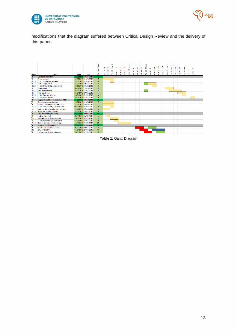
13
modifications that the diagram suffered between Critical Design Review and the delivery of
this paper.
Table 1: Gantt Diagram
14
2. Background:
2.1. OFDM (Orthogonal Frequency Division Multiplexing)
2.1.1. Concept and Definition
OFDM is one of the most used and popular modulation systems in communications
nowadays. It is widely used in different current services like 4G, wireless Networks, digital
television…
It is mentioned and briefly explained in this section due to the fact that it keeps a
close relationship with Nyquist modulation as it is going to be explained later.
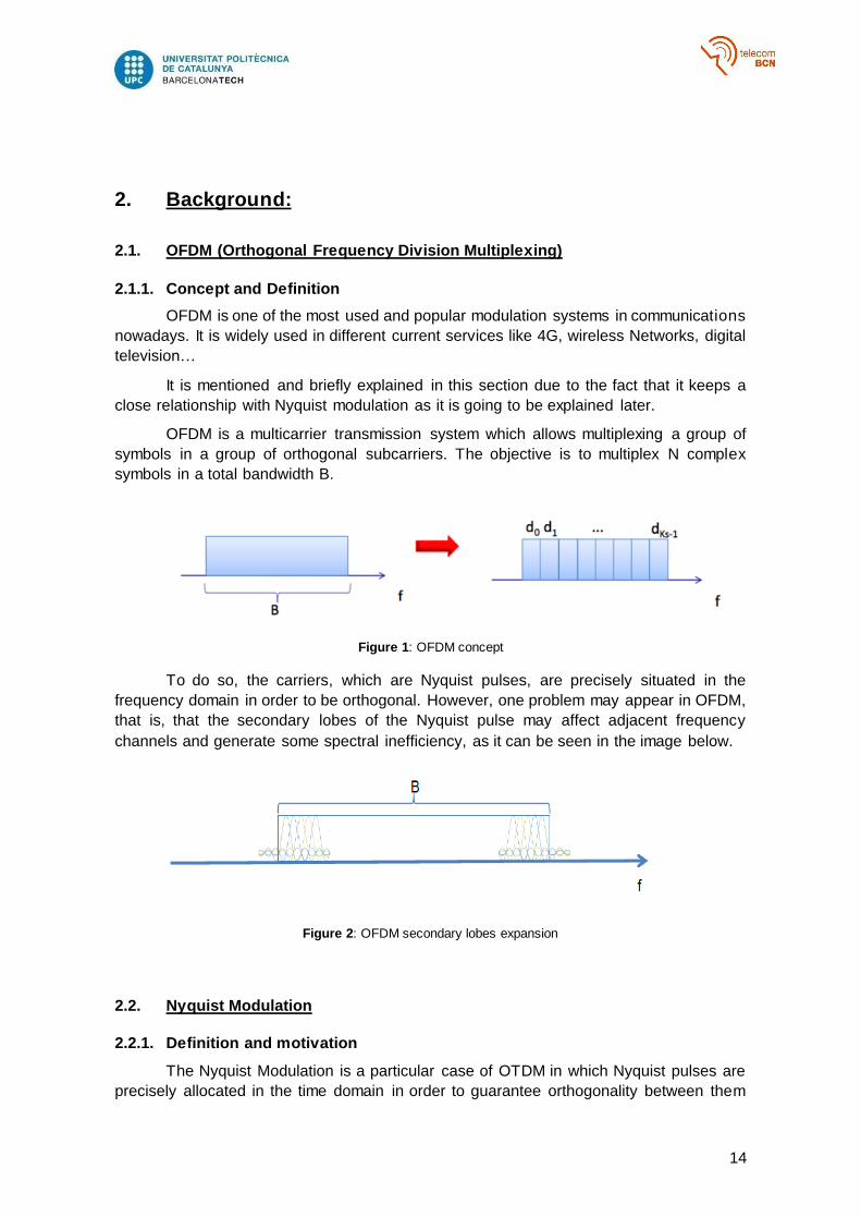
OFDM is a multicarrier transmission system which allows multiplexing a group of
symbols in a group of orthogonal subcarriers. The objective is to multiplex N complex
symbols in a total bandwidth B.
Figure 1: OFDM concept
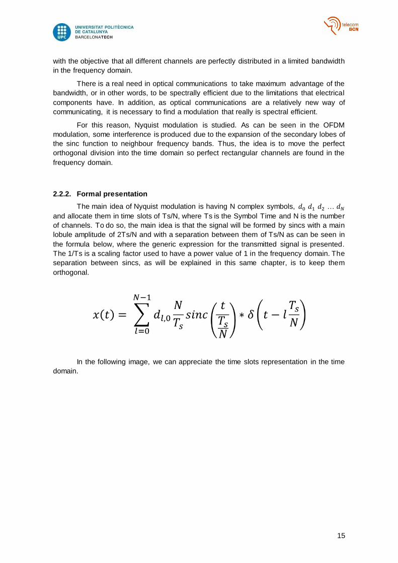
To do so, the carriers, which are Nyquist pulses, are precisely situated in the
frequency domain in order to be orthogonal. However, one problem may appear in OFDM,
that is, that the secondary lobes of the Nyquist pulse may affect adjacent frequency
channels and generate some spectral inefficiency, as it can be seen in the image below.
Figure 2: OFDM secondary lobes expansion
2.2. Nyquist Modulation
2.2.1. Definition and motivation
The Nyquist Modulation is a particular case of OTDM in which Nyquist pulses are
precisely allocated in the time domain in order to guarantee orthogonality between them
15
with the objective that all different channels are perfectly distributed in a limited bandwidth
in the frequency domain.
There is a real need in optical communications to take maximum advantage of the
bandwidth, or in other words, to be spectrally efficient due to the limitations that electrical
components have. In addition, as optical communications are a relatively new way of
communicating, it is necessary to find a modulation that really is spectral efficient.
For this reason, Nyquist modulation is studied. As can be seen in the OFDM
modulation, some interference is produced due to the expansion of the secondary lobes of
the sinc function to neighbour frequency bands. Thus, the idea is to move the perfect
orthogonal division into the time domain so perfect rectangular channels are found in the
frequency domain.
2.2.2. Formal presentation
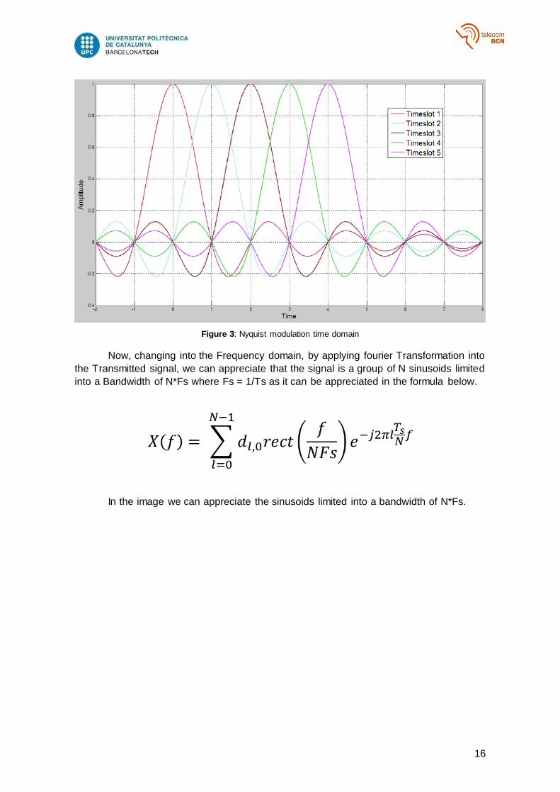
The main idea of Nyquist modulation is having N complex symbols, 𝑑0 𝑑1 𝑑2 … 𝑑𝑁
and allocate them in time slots of Ts/N, where Ts is the Symbol Time and N is the number
of channels. To do so, the main idea is that the signal will be formed by sincs with a main
lobule amplitude of 2Ts/N and with a separation between them of Ts/N as can be seen in
the formula below, where the generic expression for the transmitted signal is presented.
The 1/Ts is a scaling factor used to have a power value of 1 in the frequency domain. The
separation between sincs, as will be explained in this same chapter, is to keep them
orthogonal.
In the following image, we can appreciate the time slots representation in the time
domain.
16
Figure 3: Nyquist modulation time domain
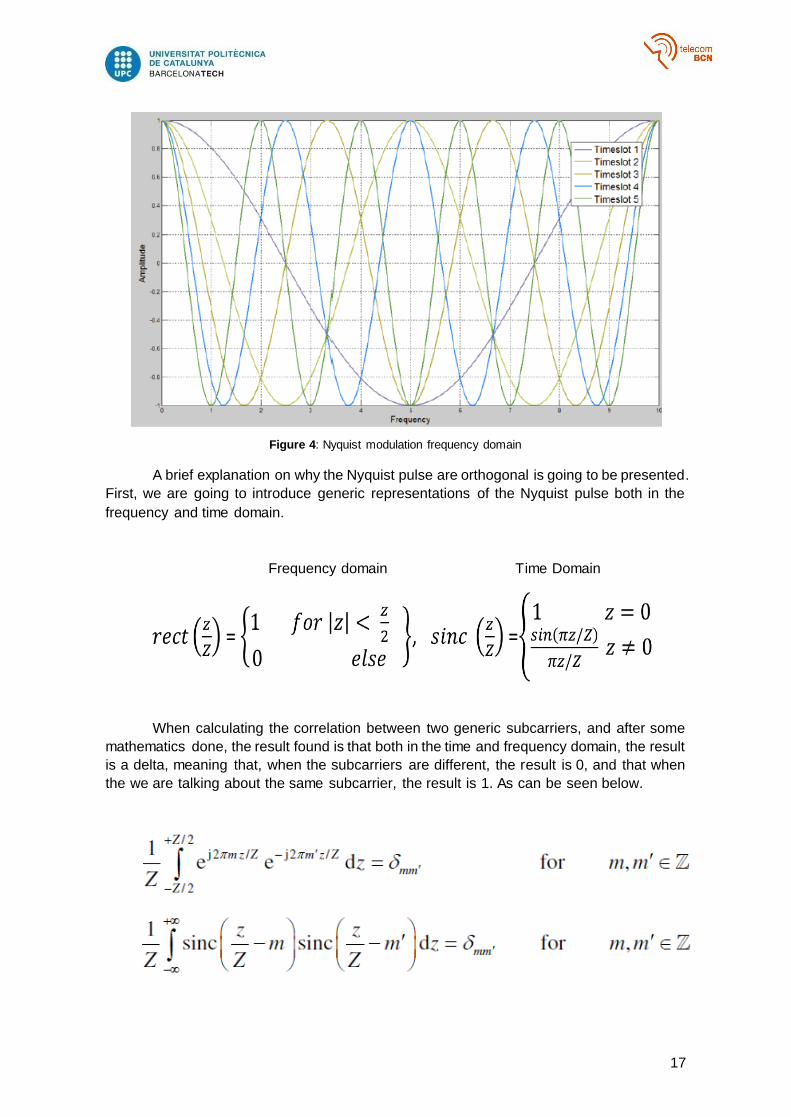
Now, changing into the Frequency domain, by applying fourier Transformation into
the Transmitted signal, we can appreciate that the signal is a group of N sinusoids limited
into a Bandwidth of N*Fs where Fs = 1/Ts as it can be appreciated in the formula below.
In the image we can appreciate the sinusoids limited into a bandwidth of N*Fs.
17
Figure 4: Nyquist modulation frequency domain
A brief explanation on why the Nyquist pulse are orthogonal is going to be presented.
First, we are going to introduce generic representations of the Nyquist pulse both in the
frequency and time domain.
Frequency domain Time Domain
When calculating the correlation between two generic subcarriers, and after some
mathematics done, the result found is that both in the time and frequency domain, the result
is a delta, meaning that, when the subcarriers are different, the result is 0, and that when
the we are talking about the same subcarrier, the result is 1. As can be seen below.
18
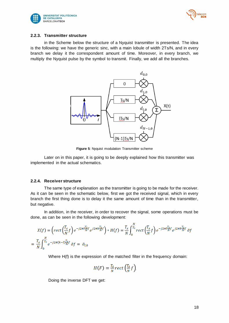
2.2.3. Transmitter structure
in the Scheme below the structure of a Nyquist transmitter is presented. The idea
is the following: we have the generic sinc, with a main lobule of width 2Ts/N, and in every
branch we delay it the correspondent amount of time. Moreover, in every branch, we
multiply the Nyquist pulse by the symbol to transmit. Finally, we add all the branches.
Figure 5: Nyquist modulation Transmitter scheme
Later on in this paper, it is going to be deeply explained how this transmitter was
implemented in the actual schematics.
2.2.4. Receiver structure
The same type of explanation as the transmitter is going to be made for the receiver.
As it can be seen in the schematic below, first we got the received signal, which in every
branch the first thing done is to delay it the same amount of time than in the transmitter,
but negative.
In addition, in the receiver, in order to recover the signal, some operations must be
done, as can be seen in the following development:
Where H(f) is the expression of the matched filter in the frequency domain:
Doing the inverse DFT we get:
19
Only when k=l, the system recovers the original signal. If k is different from l, the
signal is delayed a multiple of Ts/N that as explained in the orthogonality part the product
of the signal is 0.
Figure 6: Nyquist modulation receiver scheme
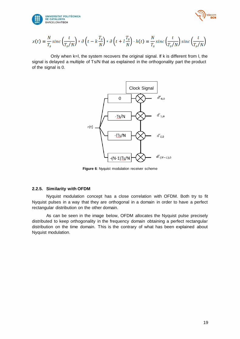
2.2.5. Similarity with OFDM
Nyquist modulation concept has a close correlation with OFDM. Both try to fit
Nyquist pulses in a way that they are orthogonal in a domain in order to have a perfect
rectangular distribution on the other domain.
As can be seen in the image below, OFDM allocates the Nyquist pulse precisely
distributed to keep orthogonality in the frequency domain obtaining a perfect rectangular
distribution on the time domain. This is the contrary of what has been explained about
Nyquist modulation.
Clock Signal
20
Nyquist OFDM
Figure 7: Comparison between Nyquist modulation and OFDM
2.3. Nyquist Multiplexing
2.3.1. Concept
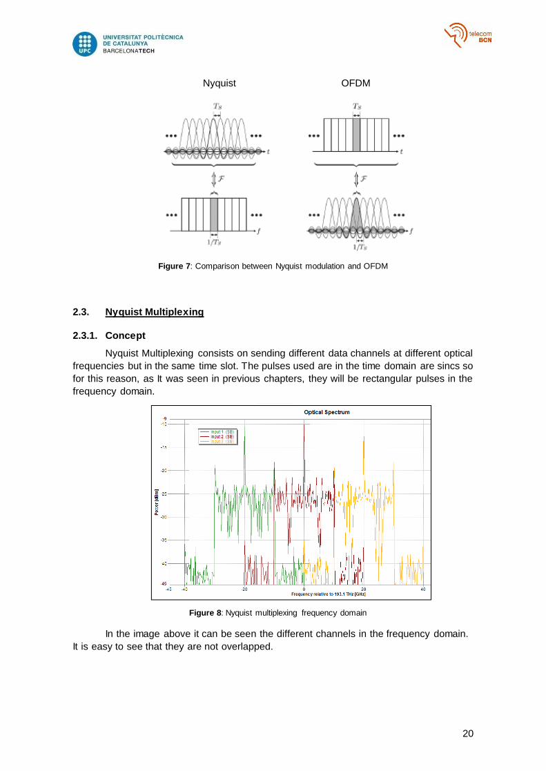
Nyquist Multiplexing consists on sending different data channels at different optical
frequencies but in the same time slot. The pulses used are in the time domain are sincs so
for this reason, as It was seen in previous chapters, they will be rectangular pulses in the
frequency domain.
Figure 8: Nyquist multiplexing frequency domain
In the image above it can be seen the different channels in the frequency domain.
It is easy to see that they are not overlapped.
21
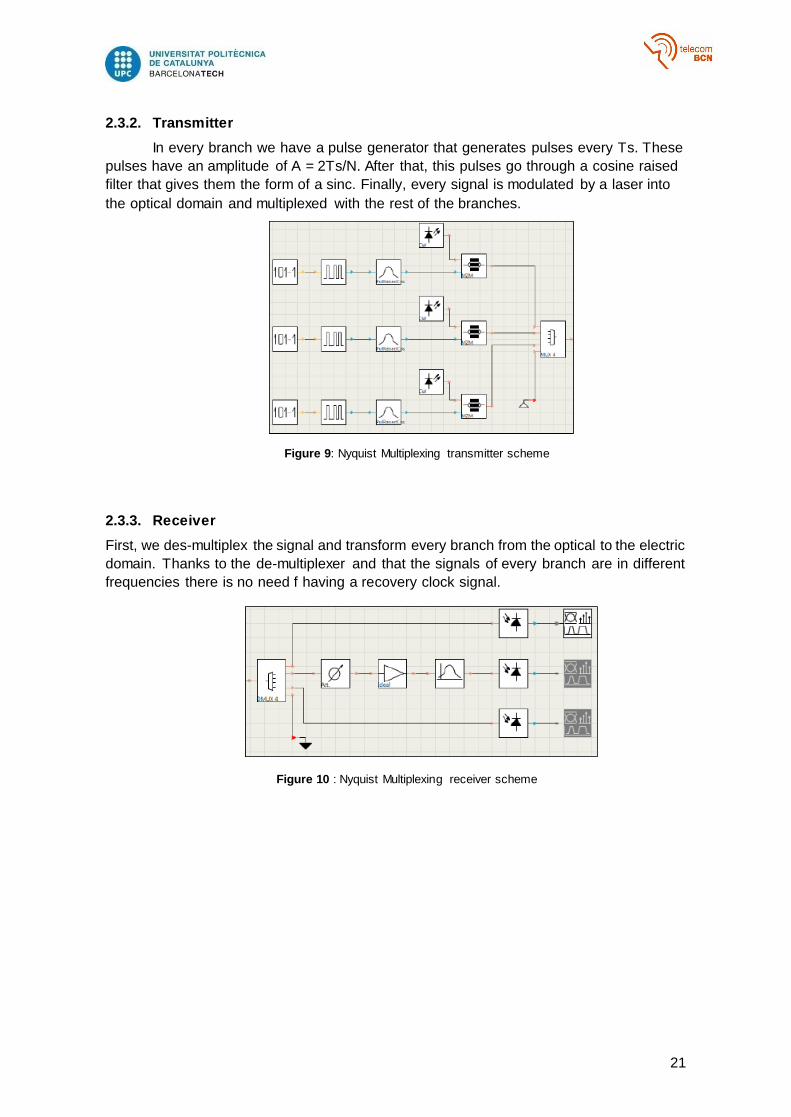
2.3.2. Transmitter
In every branch we have a pulse generator that generates pulses every Ts. These
pulses have an amplitude of A = 2Ts/N. After that, this pulses go through a cosine raised
filter that gives them the form of a sinc. Finally, every signal is modulated by a laser into
the optical domain and multiplexed with the rest of the branches.
Figure 9: Nyquist Multiplexing transmitter scheme
2.3.3. Receiver
First, we des-multiplex the signal and transform every branch from the optical to the electric
domain. Thanks to the de-multiplexer and that the signals of every branch are in different
frequencies there is no need f having a recovery clock signal.
Figure 10 : Nyquist Multiplexing receiver scheme
22
3. Methodology / project development:
3.1. Introduction
During the development of this paper VPI Transmission Maker, from VPI photonics,
was used. VPI is a powerful software that allow us to carry on simulations both in the optical
and electrical domain and in different scenarios.
In this thesis, the main point was to observe how Nyquist modulation behaves in
the optical world. However, in order to fully understand how the Nyquist modulation works
simpler schematics were designed. In this part of the thesis, we are going to present the
different schematics used during the process in order to understand Nyquist modulation
and the final schematics from where the results were taken. To begin with, a brief
explanation on which are the main parameters to bear in mind while using this software is
presented.
Firstly, the TimeWindow, sets the period of real time that is represented as a block
of data. It also sets the spectral resolution. Secondly, the SampleRateDefault. It used by
default in all modules as a sample rate parameter. However, each module can have his
own sample rate. Finally, the BitRateDefault, is used by default by all modules as a bit rate
parameter. Each module however, can set a different bit rate.
These parameters were set differently depending on if a QAM modulation was used
or not. In order to have the same number of symbols when using a QAM modulation or one
simpler TimeWindow and SampleRateDefault were multiplied by the number of bits used
in that specific modulation.
3.2. Nyquist Modulation
In order to set a start point, the first and simplest module studied was the Nyquist
modulation. In this section, we are going to deeply explain how we implemented the
different parts of a Nyquist Modulation system that will be used in other schematics in the
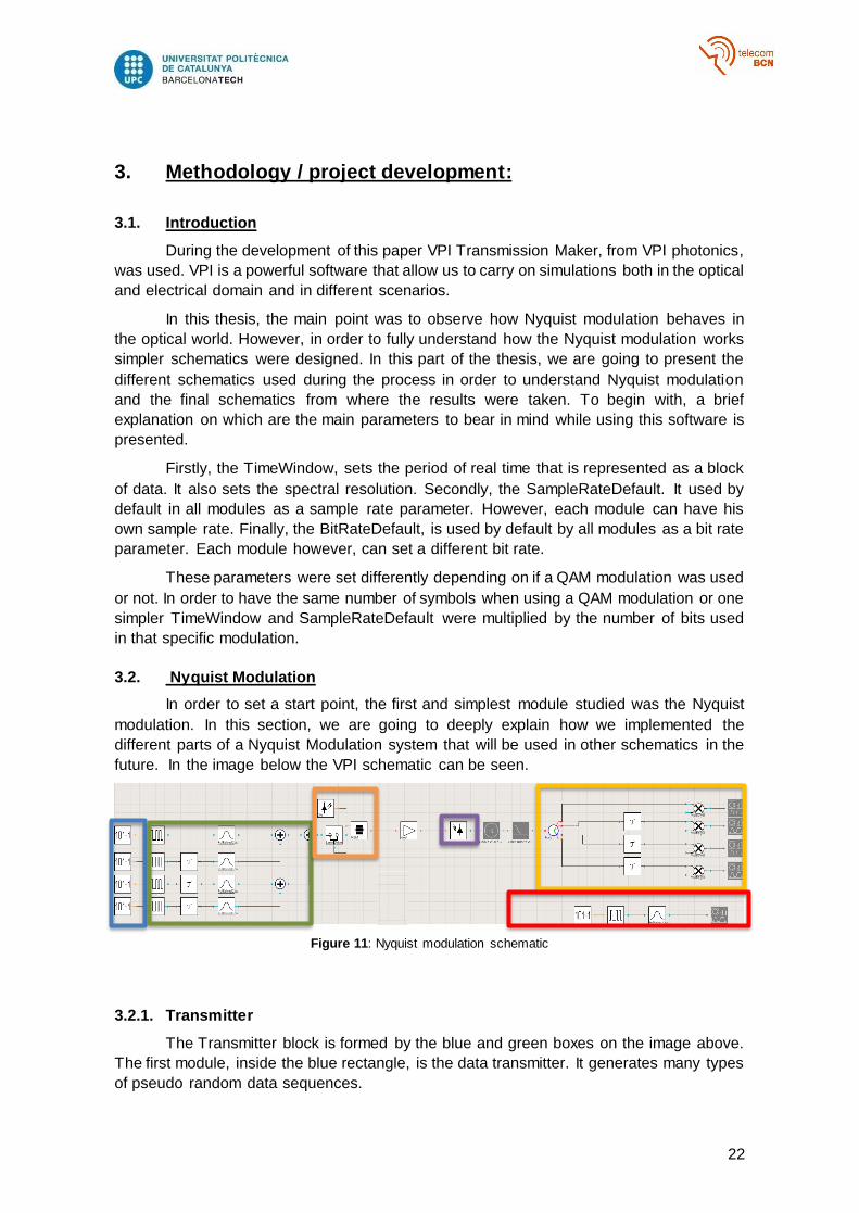
future. In the image below the VPI schematic can be seen.
Figure 11: Nyquist modulation schematic
3.2.1. Transmitter
The Transmitter block is formed by the blue and green boxes on the image above.
The first module, inside the blue rectangle, is the data transmitter. It generates many types
of pseudo random data sequences.
23
The second box, the green one, is where the Nyquist encoder is set. modules on
the left of this box are the coders. These modules generate a sampled RZ (Return to Zero)
coded signal defined by a sequence of bits at its input. The next modules are delayers.
They delay the signal in order to maintain the orthogonality explained in the second part of
this paper. In order to calculate the delay, first we have to know the main lobe width of the
Nyquist pulse. For this reason, the next module it is going to be presented. This module
generates a Nyquist response from an incoming electrical impulse. Finally, the 4 channels
are joined.
In addition, and inside an orange rectangle, the electric-optic step is found. As its
name clearly indicates, it transforms the electric signal into optical.It is formed by 3 different
modules, consisting on: On the top of the square, a laser, which generates a continuous
wave optical signal, connected to a Mach-Zehender modulator, which modulates in
intensity signal light using a simple drive circuit. Finally, a laser driver is added in order to
have the electrical signal in the amplitude range where it can be perfectly modulated by the
Mach-Zender.
First, we have to set the width of the main lobe. As it can be seen in the schematic,
we have four different channels. The main idea of Nyquist modulation is to be capable of
fit the 4 channels in the time of bit. The time of bit, Ts, having a bit rate of 10GHz is 100ps.
So, in order to fit the 4 channels in 100ps, we have to divide 100ps by 4, resulting 100𝑝𝑠
4=
25𝑝𝑠 . In order to achieve that in the schematic, we set the parameter SymbolRate to
4*BitRateDefault.
Now, it is time to set the delay between the different channels. In order to keep the
orthogonality between the channels, the delay has to be equal to the width of the main lobe.
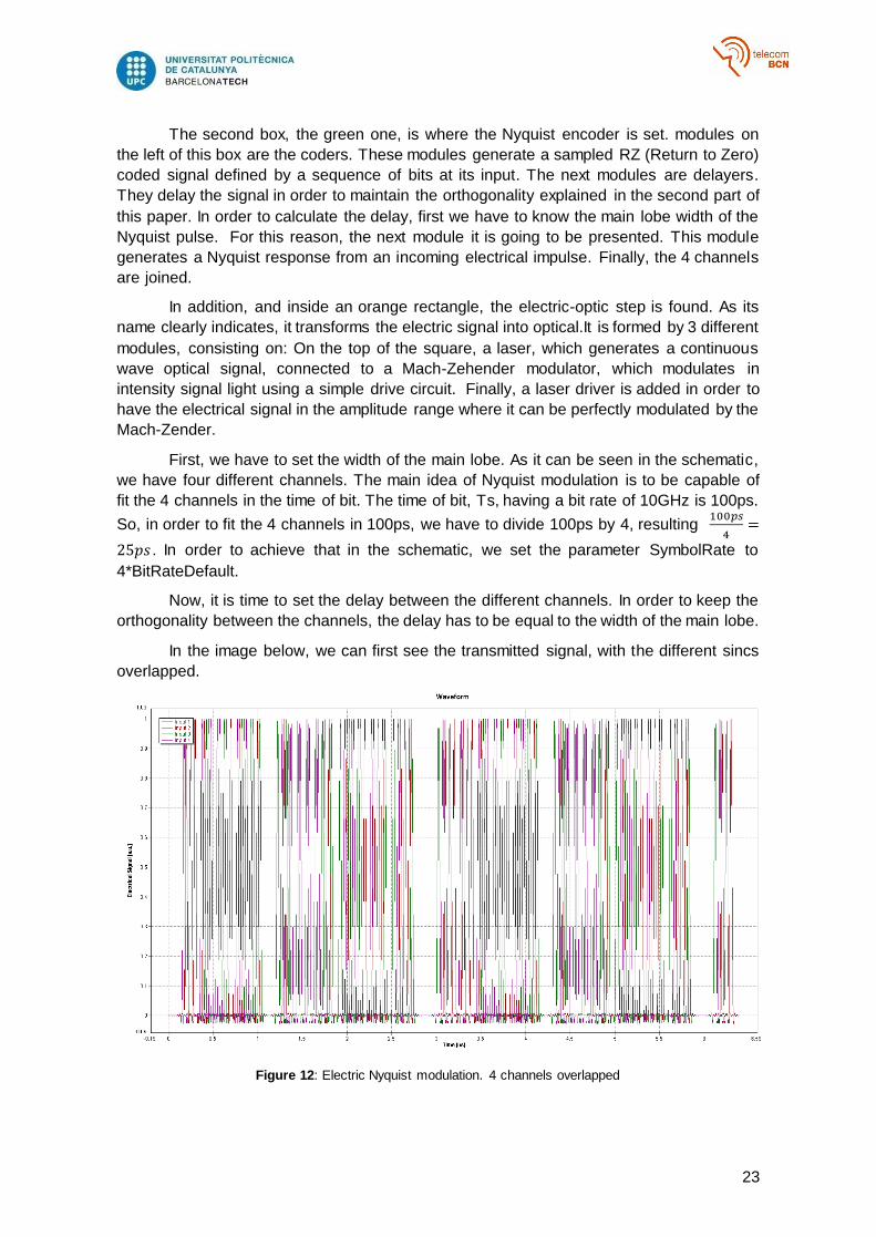
In the image below, we can first see the transmitted signal, with the different sincs
overlapped.
Figure 12: Electric Nyquist modulation. 4 channels overlapped
24
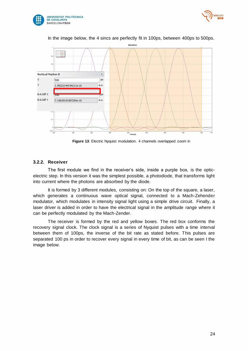
In the image below, the 4 sincs are perfectly fit in 100ps, between 400ps to 500ps.
Figure 13: Electric Nyquist modulation. 4 channels overlapped zoom in
3.2.2. Receiver
The first module we find in the receiver’s side, inside a purple box, is the optic-
electric step. In this version it was the simplest possible, a photodiode, that transforms light
into current where the photons are absorbed by the diode.
It is formed by 3 different modules, consisting on: On the top of the square, a laser,
which generates a continuous wave optical signal, connected to a Mach-Zehender
modulator, which modulates in intensity signal light using a simple drive circuit. Finally, a
laser driver is added in order to have the electrical signal in the amplitude range where it
can be perfectly modulated by the Mach-Zender.
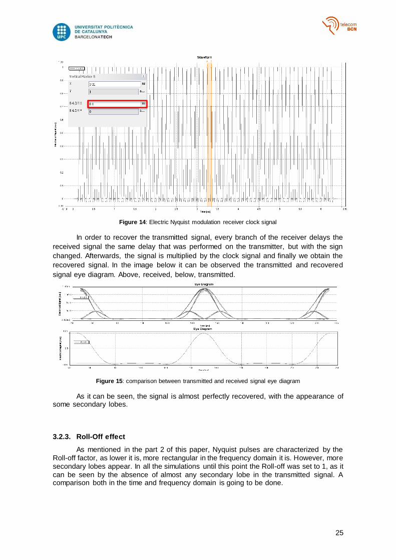
The receiver is formed by the red and yellow boxes. The red box conforms the
recovery signal clock. The clock signal is a series of Nyquist pulses with a time interval
between them of 100ps, the inverse of the bit rate as stated before. This pulses are
separated 100 ps in order to recover every signal in every time of bit, as can be seen I the
image below.
25
Figure 14: Electric Nyquist modulation receiver clock signal
In order to recover the transmitted signal, every branch of the receiver delays the
received signal the same delay that was performed on the transmitter, but with the sign
changed. Afterwards, the signal is multiplied by the clock signal and finally we obtain the
recovered signal. In the image below it can be observed the transmitted and recovered
signal eye diagram. Above, received, below, transmitted.
Figure 15: comparison between transmitted and received signal eye diagram
As it can be seen, the signal is almost perfectly recovered, with the appearance of some secondary lobes.
3.2.3. Roll-Off effect
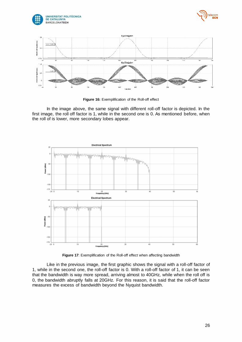
As mentioned in the part 2 of this paper, Nyquist pulses are characterized by the Roll-off factor, as lower it is, more rectangular in the frequency domain it is. However, more secondary lobes appear. In all the simulations until this point the Roll-off was set to 1, as it can be seen by the absence of almost any secondary lobe in the transmitted signal. A comparison both in the time and frequency domain is going to be done.
26
Figure 16: Exemplification of the Roll-off effect
In the image above, the same signal with different roll-off factor is depicted. In the first image, the roll off factor is 1, while in the second one is 0. As mentioned before, when the roll of is lower, more secondary lobes appear.
Figure 17: Exemplification of the Roll-off effect when affecting bandwidth
Like in the previous image, the first graphic shows the signal with a roll-off factor of 1, while in the second one, the roll-off factor is 0. With a roll-off factor of 1, it can be seen that the bandwidth is way more spread, arriving almost to 40GHz, while when the roll off is
0, the bandwidth abruptly falls at 20GHz. For this reason, it is said that the roll-off factor measures the excess of bandwidth beyond the Nyquist bandwidth.
27
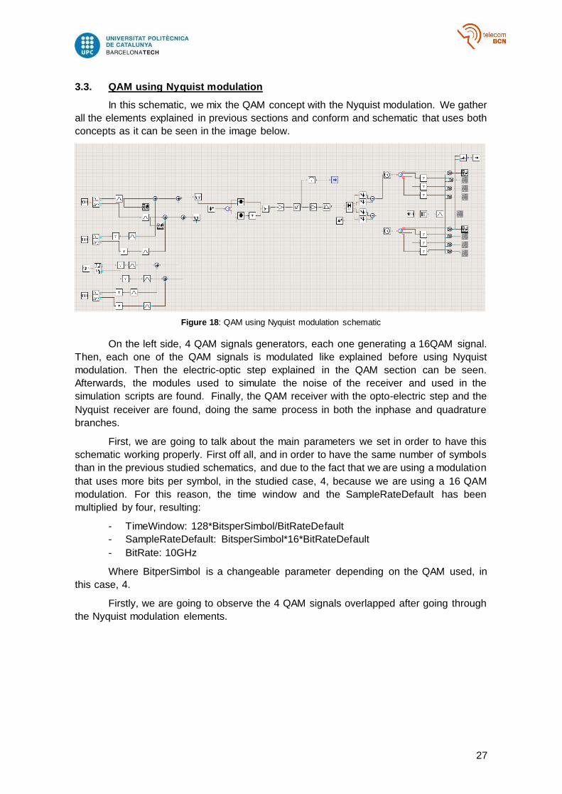
3.3. QAM using Nyquist modulation
In this schematic, we mix the QAM concept with the Nyquist modulation. We gather
all the elements explained in previous sections and conform and schematic that uses both
concepts as it can be seen in the image below.
Figure 18: QAM using Nyquist modulation schematic
On the left side, 4 QAM signals generators, each one generating a 16QAM signal.
Then, each one of the QAM signals is modulated like explained before using Nyquist
modulation. Then the electric-optic step explained in the QAM section can be seen.
Afterwards, the modules used to simulate the noise of the receiver and used in the
simulation scripts are found. Finally, the QAM receiver with the opto-electric step and the
Nyquist receiver are found, doing the same process in both the inphase and quadrature
branches.
First, we are going to talk about the main parameters we set in order to have this
schematic working properly. First off all, and in order to have the same number of symbols
than in the previous studied schematics, and due to the fact that we are using a modulation
that uses more bits per symbol, in the studied case, 4, because we are using a 16 QAM
modulation. For this reason, the time window and the SampleRateDefault has been
multiplied by four, resulting:
- TimeWindow: 128*BitsperSimbol/BitRateDefault
- SampleRateDefault: BitsperSimbol*16*BitRateDefault
- BitRate: 10GHz
Where BitperSimbol is a changeable parameter depending on the QAM used, in
this case, 4.
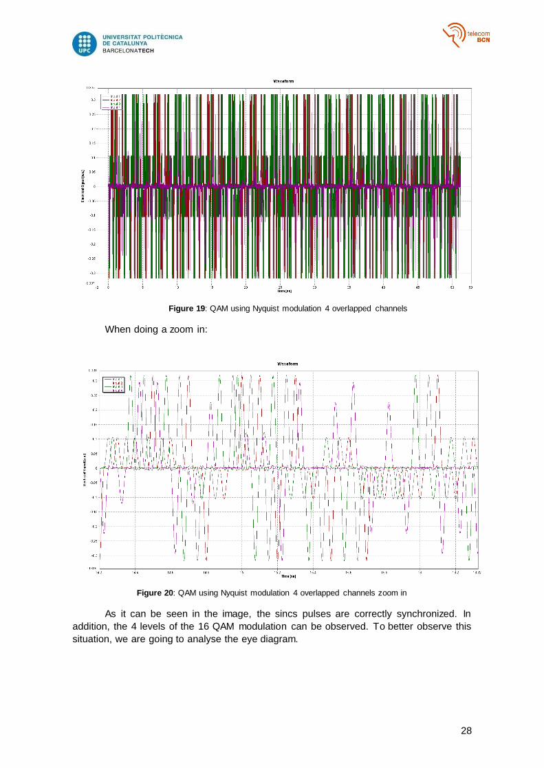
Firstly, we are going to observe the 4 QAM signals overlapped after going through
the Nyquist modulation elements.
28
Figure 19: QAM using Nyquist modulation 4 overlapped channels
When doing a zoom in:
Figure 20: QAM using Nyquist modulation 4 overlapped channels zoom in
As it can be seen in the image, the sincs pulses are correctly synchronized. In
addition, the 4 levels of the 16 QAM modulation can be observed. To better observe this
situation, we are going to analyse the eye diagram.
29
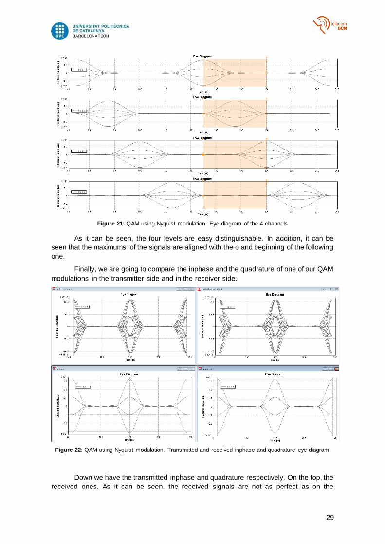
Figure 21: QAM using Nyquist modulation. Eye diagram of the 4 channels
As it can be seen, the four levels are easy distinguishable. In addition, it can be
seen that the maximums of the signals are aligned with the o and beginning of the following
one.
Finally, we are going to compare the inphase and the quadrature of one of our QAM
modulations in the transmitter side and in the receiver side.
Figure 22: QAM using Nyquist modulation. Transmitted and received inphase and quadrature eye diagram
Down we have the transmitted inphase and quadrature respectively. On the top, the
received ones. As it can be seen, the received signals are not as perfect as on the
30
transmission side, However, in the important points, the ones in the middle, the 4 levels
are perfectly distinguished.
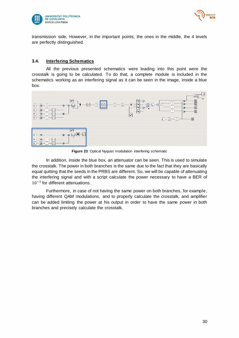
3.4. Interfering Schematics
All the previous presented schematics were leading into this point were the
crosstalk is going to be calculated. To do that, a complete module is included in the
schematics working as an interfering signal as it can be seen in the image, inside a blue
box.
Figure 23: Optical Nyquist modulation interfering schematic
In addition, inside the blue box, an attenuator can be seen. This is used to simulate
the crosstalk. The power in both branches is the same due to the fact that they are basically
equal quitting that the seeds in the PRBS are different. So, we will be capable of attenuating
the interfering signal and with a script calculate the power necessary to have a BER of
10−3 for different attenuations.
Furthermore, in case of not having the same power on both branches, for example,
having different QAM modulations, and to properly calculate the crosstalk, and amplifier
can be added limiting the power at his output in order to have the same power in both
branches and precisely calculate the crosstalk.
31
4. Results
In this section, the results obtained after using some simulation scripts in order to
obtain crosstalk results between different type of modulations are going to be presented.
The simulation script used to calculate the crosstalk level can be found in the
appendices. However, a brief explanation of its functionality is going to be made. The
simulation reduces or increases the attenuation of the attenuator in the middle of the optical
signal (inside a blue square in image 34) depending if the BER is over 10−3. Each step,
this change on the attenuation gets smaller until reaching a pre-set point. This process is
developed for every crosstalk level.
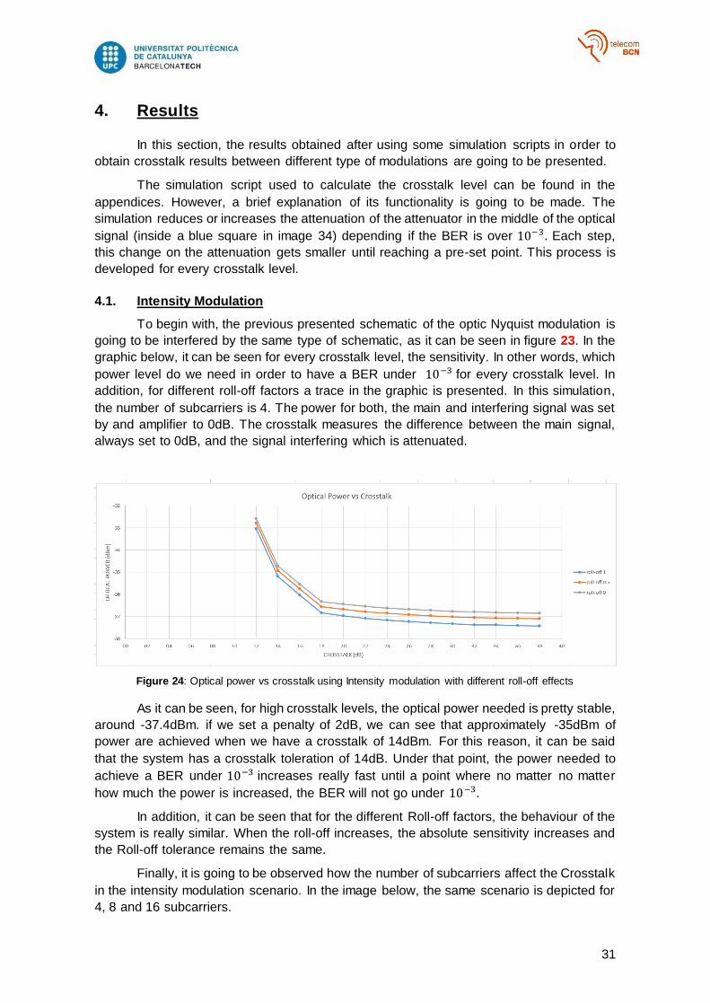
4.1. Intensity Modulation
To begin with, the previous presented schematic of the optic Nyquist modulation is
going to be interfered by the same type of schematic, as it can be seen in figure 23. In the
graphic below, it can be seen for every crosstalk level, the sensitivity. In other words, which
power level do we need in order to have a BER under 10−3 for every crosstalk level. In
addition, for different roll-off factors a trace in the graphic is presented. In this simulation,
the number of subcarriers is 4. The power for both, the main and interfering signal was set
by and amplifier to 0dB. The crosstalk measures the difference between the main signal,
always set to 0dB, and the signal interfering which is attenuated.
Figure 24: Optical power vs crosstalk using Intensity modulation with different roll-off effects
As it can be seen, for high crosstalk levels, the optical power needed is pretty stable,
around -37.4dBm. if we set a penalty of 2dB, we can see that approximately -35dBm of
power are achieved when we have a crosstalk of 14dBm. For this reason, it can be said
that the system has a crosstalk toleration of 14dB. Under that point, the power needed to
achieve a BER under 10−3 increases really fast until a point where no matter no matter
how much the power is increased, the BER will not go under 10−3.
In addition, it can be seen that for the different Roll-off factors, the behaviour of the
system is really similar. When the roll-off increases, the absolute sensitivity increases and
the Roll-off tolerance remains the same.
Finally, it is going to be observed how the number of subcarriers affect the Crosstalk
in the intensity modulation scenario. In the image below, the same scenario is depicted for
4, 8 and 16 subcarriers.
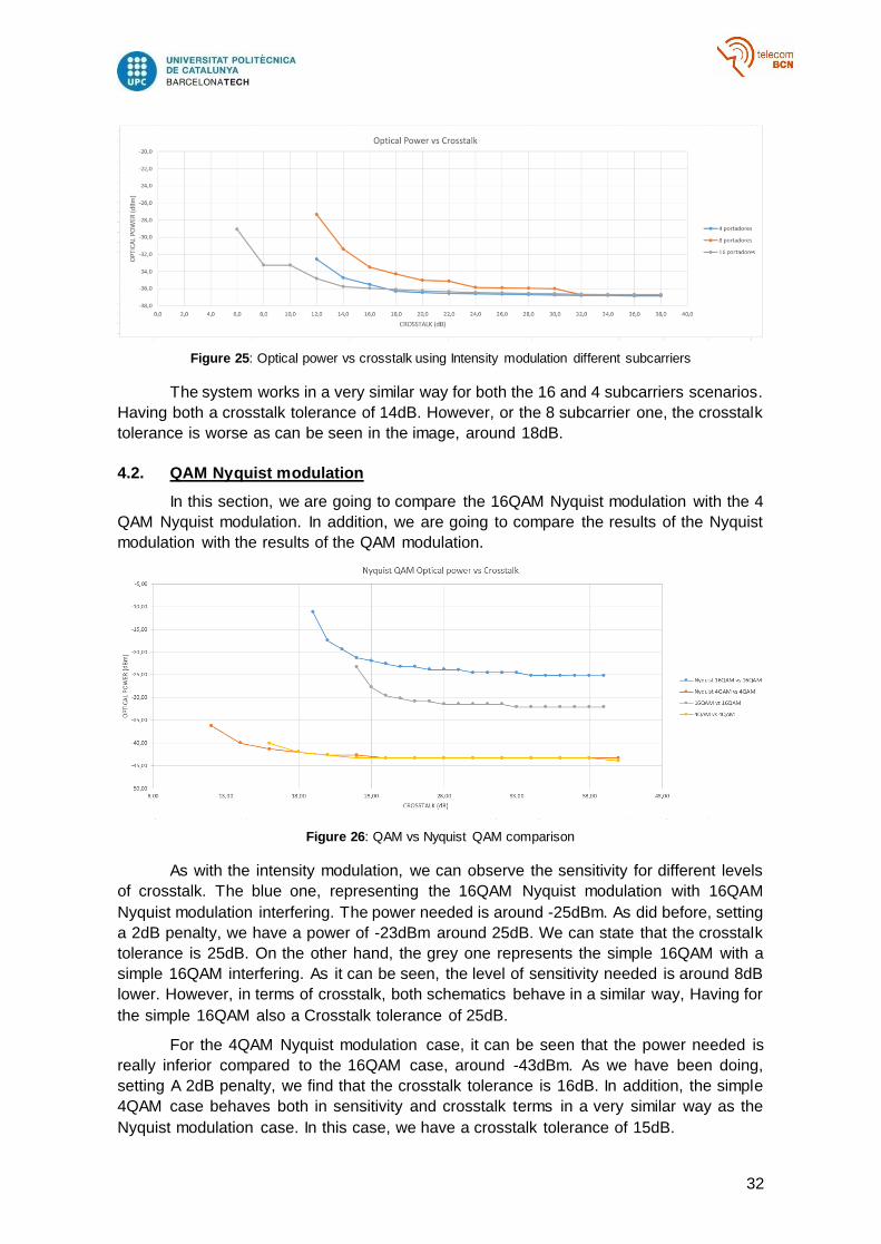
32
Figure 25: Optical power vs crosstalk using Intensity modulation different subcarriers
The system works in a very similar way for both the 16 and 4 subcarriers scenarios.
Having both a crosstalk tolerance of 14dB. However, or the 8 subcarrier one, the crosstalk
tolerance is worse as can be seen in the image, around 18dB.
4.2. QAM Nyquist modulation
In this section, we are going to compare the 16QAM Nyquist modulation with the 4
QAM Nyquist modulation. In addition, we are going to compare the results of the Nyquist
modulation with the results of the QAM modulation.
Figure 26: QAM vs Nyquist QAM comparison
As with the intensity modulation, we can observe the sensitivity for different levels
of crosstalk. The blue one, representing the 16QAM Nyquist modulation with 16QAM
Nyquist modulation interfering. The power needed is around -25dBm. As did before, setting
a 2dB penalty, we have a power of -23dBm around 25dB. We can state that the crosstalk
tolerance is 25dB. On the other hand, the grey one represents the simple 16QAM with a
simple 16QAM interfering. As it can be seen, the level of sensitivity needed is around 8dB
lower. However, in terms of crosstalk, both schematics behave in a similar way, Having for
the simple 16QAM also a Crosstalk tolerance of 25dB.
For the 4QAM Nyquist modulation case, it can be seen that the power needed is
really inferior compared to the 16QAM case, around -43dBm. As we have been doing,
setting A 2dB penalty, we find that the crosstalk tolerance is 16dB. In addition, the simple
4QAM case behaves both in sensitivity and crosstalk terms in a very similar way as the
Nyquist modulation case. In this case, we have a crosstalk tolerance of 15dB.
33
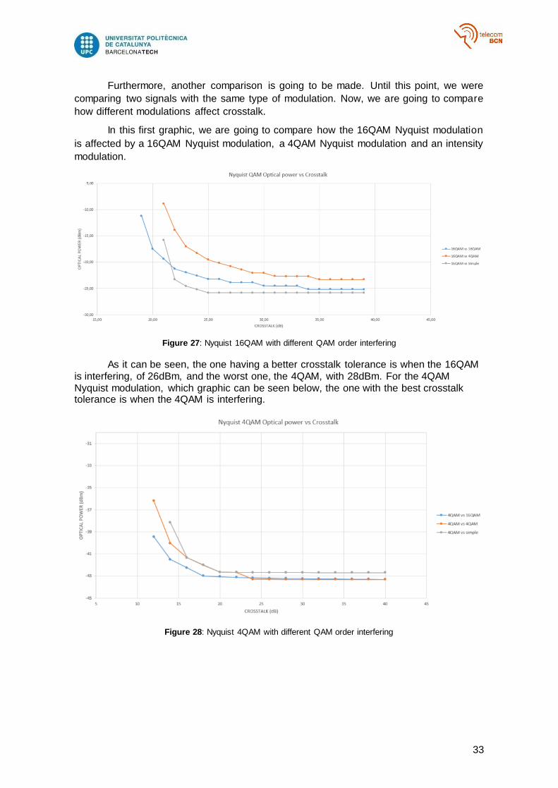
Furthermore, another comparison is going to be made. Until this point, we were
comparing two signals with the same type of modulation. Now, we are going to compare
how different modulations affect crosstalk.
In this first graphic, we are going to compare how the 16QAM Nyquist modulation
is affected by a 16QAM Nyquist modulation, a 4QAM Nyquist modulation and an intensity
modulation.
Figure 27: Nyquist 16QAM with different QAM order interfering
As it can be seen, the one having a better crosstalk tolerance is when the 16QAM is interfering, of 26dBm, and the worst one, the 4QAM, with 28dBm. For the 4QAM Nyquist modulation, which graphic can be seen below, the one with the best crosstalk tolerance is when the 4QAM is interfering.
Figure 28: Nyquist 4QAM with different QAM order interfering
34
5. Budget
Table 2: Budget
35
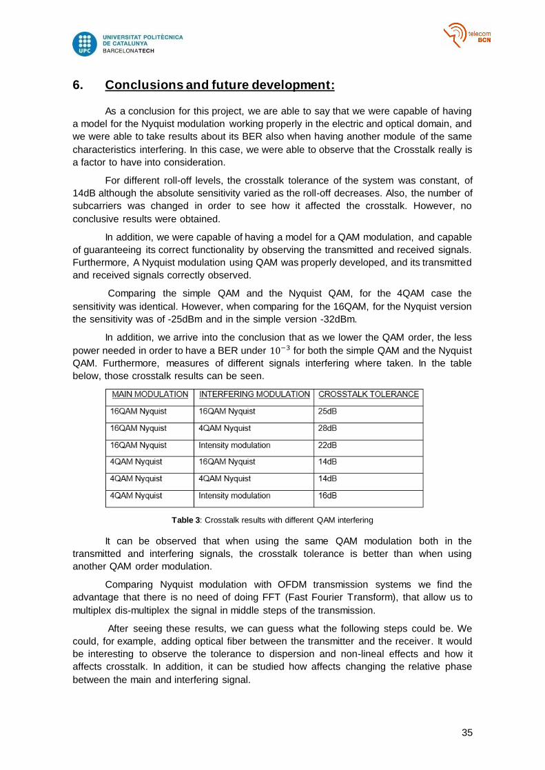
6. Conclusions and future development:
As a conclusion for this project, we are able to say that we were capable of having
a model for the Nyquist modulation working properly in the electric and optical domain, and
we were able to take results about its BER also when having another module of the same
characteristics interfering. In this case, we were able to observe that the Crosstalk really is
a factor to have into consideration.
For different roll-off levels, the crosstalk tolerance of the system was constant, of
14dB although the absolute sensitivity varied as the roll-off decreases. Also, the number of
subcarriers was changed in order to see how it affected the crosstalk. However, no
conclusive results were obtained.
In addition, we were capable of having a model for a QAM modulation, and capable
of guaranteeing its correct functionality by observing the transmitted and received signals.
Furthermore, A Nyquist modulation using QAM was properly developed, and its transmitted
and received signals correctly observed.
Comparing the simple QAM and the Nyquist QAM, for the 4QAM case the
sensitivity was identical. However, when comparing for the 16QAM, for the Nyquist version
the sensitivity was of -25dBm and in the simple version -32dBm.
In addition, we arrive into the conclusion that as we lower the QAM order, the less
power needed in order to have a BER under 10−3 for both the simple QAM and the Nyquist
QAM. Furthermore, measures of different signals interfering where taken. In the table
below, those crosstalk results can be seen.
Table 3: Crosstalk results with different QAM interfering
It can be observed that when using the same QAM modulation both in the
transmitted and interfering signals, the crosstalk tolerance is better than when using
another QAM order modulation.
Comparing Nyquist modulation with OFDM transmission systems we find the
advantage that there is no need of doing FFT (Fast Fourier Transform), that allow us to
multiplex dis-multiplex the signal in middle steps of the transmission.
After seeing these results, we can guess what the following steps could be. We
could, for example, adding optical fiber between the transmitter and the receiver. It would
be interesting to observe the tolerance to dispersion and non-lineal effects and how it
affects crosstalk. In addition, it can be studied how affects changing the relative phase
between the main and interfering signal.

36
Apart of that, we did all the simulations under an ideal point of view, supposing all
the elements used on the schematics to be ideal. It could be interesting to see how a
desynchronization between the clock and the transmitter would affect. In addition, in a
realistic system, the length of the Nyquist pulses should be limited, not like in an ideal
environment, where the longer those pulses are, the better.
37
Bibliography:
[1] Alba Pagès, ICOM. Chapter III.2: IQ modulation and coherent demodulation.
[2] Gregori Vazquez, CDA. Chapter 3: Frequency selective channels.
[3] Joan M. Gené, TC. Chapter 5: Optical Receivers.
[4] Joan M. Gené, TC. Chapter 4: Optical Transmitters.
[5] Alba Pagès, ICOM. Chapter III.2: IQ modulation and coherent demodulation.
[6] Joan M. Gené, Optical Fiber Communications. Coherent detection.
[7] Evaluation of optical OFDM signals crosstalk Tolerance. Adrià Escolano Beltran
[8] Investigation on Nyquist Modulation for Fiber-Optic Communications, Jonathan Casal Rodríguez
[9] Investigation on Nyquist Modulation and Multiplexing for Fiber Optic Communications, Marc Jubany Ticó
[10] Real-time Nyquist pulse generation beyond 100 Gbit/s and its relation to OFDMR. Schmogrow, M. Winter,
M. Meyer, D. Hillerkuss, S. Wolf, B. Baeuerle, A.Ludwig, B. Nebendahl, S. Ben-Ezra, J. Meyer, M. Dreschmann, M. Huebner, J.Becker, C. Koos, W. Freude, and J. Leuthold
[11] Performance Comparision of single-sideband Direct Detection Nyquist-subcarrier Modulation and OFDM.
M. Sezer Erkılınç, Stephan Pachnicke, Helmut Griesser, Benn C. Thomsen, Polina Bayvel, and Robert I.
Killey
[12] Spectrally efficient WDM Nyquist pulse-shaped Subcarrier Modulation Using a Dual-Drive ma
[13] Signal-signal beat interference cancellation in spectrally-efficient WDM direct-detection Nyquist-pulse-
shaped 16-QAM subcarrier modulation. Zhe Li, M. Sezer. Erkılınç, Stephan Pachnicke, Helmut Griesser, Rachid Bouziane, Benn C. Thomsen, Polina Bayvel, and Robert I. Killey
38
7. Appendices
7.1. Rest of Simulations performed during the project development
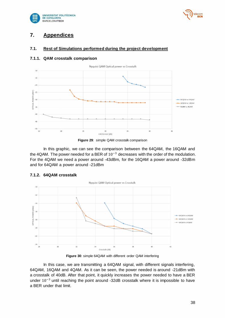
7.1.1. QAM crosstalk comparison
Figure 29: simple QAM crosstalk comparison
In this graphic, we can see the comparison between the 64QAM, the 16QAM and
the 4QAM. The power needed for a BER of 10−3 decreases with the order of the modulation.
For the 4QAM we need a power around -43dBm, for the 16QAM a power around -32dBm
and for 64QAM a power around -21dBm
7.1.2. 64QAM crosstalk
Figure 30: simple 64QAM with different order QAM interfering
In this case, we are transmitting a 64QAM signal, with different signals interfering,
64QAM, 16QAM and 4QAM. As it can be seen, the power needed is around -21dBm with
a crosstalk of 40dB. After that point, it quickly increases the power needed to have a BER
under 10−3 until reaching the point around -32dB crosstalk where it is impossible to have
a BER under that limit.
39
7.1.3. 16QAM crosstalk
Figure 31: simple 16QAM with different order QAM interfering
Similar to the Nyquist case, the power needed for the different interfering signals is similar
as well as its behaviour. For the 3 cases, we have a crosstalk tolerance of 25dB.
7.1.4. 4QAM crosstalk
Figure 32: simple 4QAM with different order QAM interfering
As before, similar to the Nyquist case, we need for the 3 cases a power around -
43dBm. In all 3 cases, we have a crosstalk tolerance of 15dB.
40
7.2. Simulation scripts
7.2.1. Crosstalk simulation script
set all "C:/Users/pfc_jgene1/Desktop/SIMULACIONS/"
append all "all.txt"
set BER_found "C:/Users/pfc_jgene1/Desktop/SIMULACIONS/"
append BER_found "BER_found.txt"
set ATT1 40.0
set ATT2 8.0
set inc 2.0
set BER 0
set BER_Trobada 0
set power 0
set ATTMax 80.0
set ATTMin 0.0
while {$ATT2 >= 0} {
while {$BER_Trobada != 1} {
setstate Attenuator_vtms1 Attenuation $ATT1;
run 1
wrapup
set BER [statevalue PostValue_vtms2 InputValue];
set power [statevalue PostValue_vtms1 InputValue];
if {[expr $BER > 1.0e-3]} {
set ATTMax $ATT1;
if {[expr ($ATTMax - $ATTMin) < 0.5]} {
set BER_Trobada 1;
} else {
set ATT1 [expr ($ATTMax + $ATTMin)/2]
}
}
if {[expr $BER < 1.0e-3]} {
set ATTMin $ATT1;
if {[expr ($ATTMax - $ATTMin) < 0.5]} {
set BER_Trobada 1;
} else {
41
set ATT1 [expr ($ATTMax + $ATTMin)/2]
}
}
set result [open $all a]
puts $result "Atenuacio (dB):"
puts $result $ATT1
puts $result "Potència Optica (dBm):"
puts $result $power
puts $result "BER:"
puts $result $BER
close $result
}
set result2 [open $BER_found a]
puts $result2 "Atenuació Interferent"
puts $result2 $ATT2
puts $result2 "Atenuacio (dB):"
puts $result2 $ATT1
puts $result2 "Potència Optica (dBm):"
puts $result2 $power
puts $result2 "SER:"
puts $result2 $BER
close $result2
set BER_Trobada 0;
set ATT2 [expr $ATT2 - $inc];
set ATT1 40.0;
set BER 0.0;
set power 0.0;
set ATTMax 80.0;
set ATTMin 0.0;
setstate Attenuator_vtms2 Attenuation $ATT2;
}
42
7.3. Raised cosine Filter
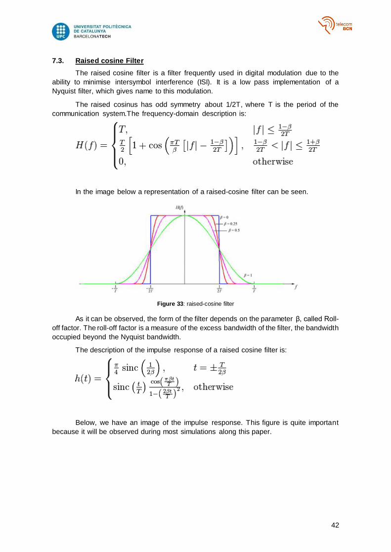
The raised cosine filter is a filter frequently used in digital modulation due to the
ability to minimise intersymbol interference (ISI). It is a low pass implementation of a
Nyquist filter, which gives name to this modulation.
The raised cosinus has odd symmetry about 1/2T, where T is the period of the
communication system.The frequency-domain description is:
In the image below a representation of a raised-cosine filter can be seen.
Figure 33: raised-cosine filter
As it can be observed, the form of the filter depends on the parameter β, called Roll-
off factor. The roll-off factor is a measure of the excess bandwidth of the filter, the bandwidth
occupied beyond the Nyquist bandwidth.
The description of the impulse response of a raised cosine filter is:
Below, we have an image of the impulse response. This figure is quite important
because it will be observed during most simulations along this paper.
43
Figure 34: raised cosine impulse response
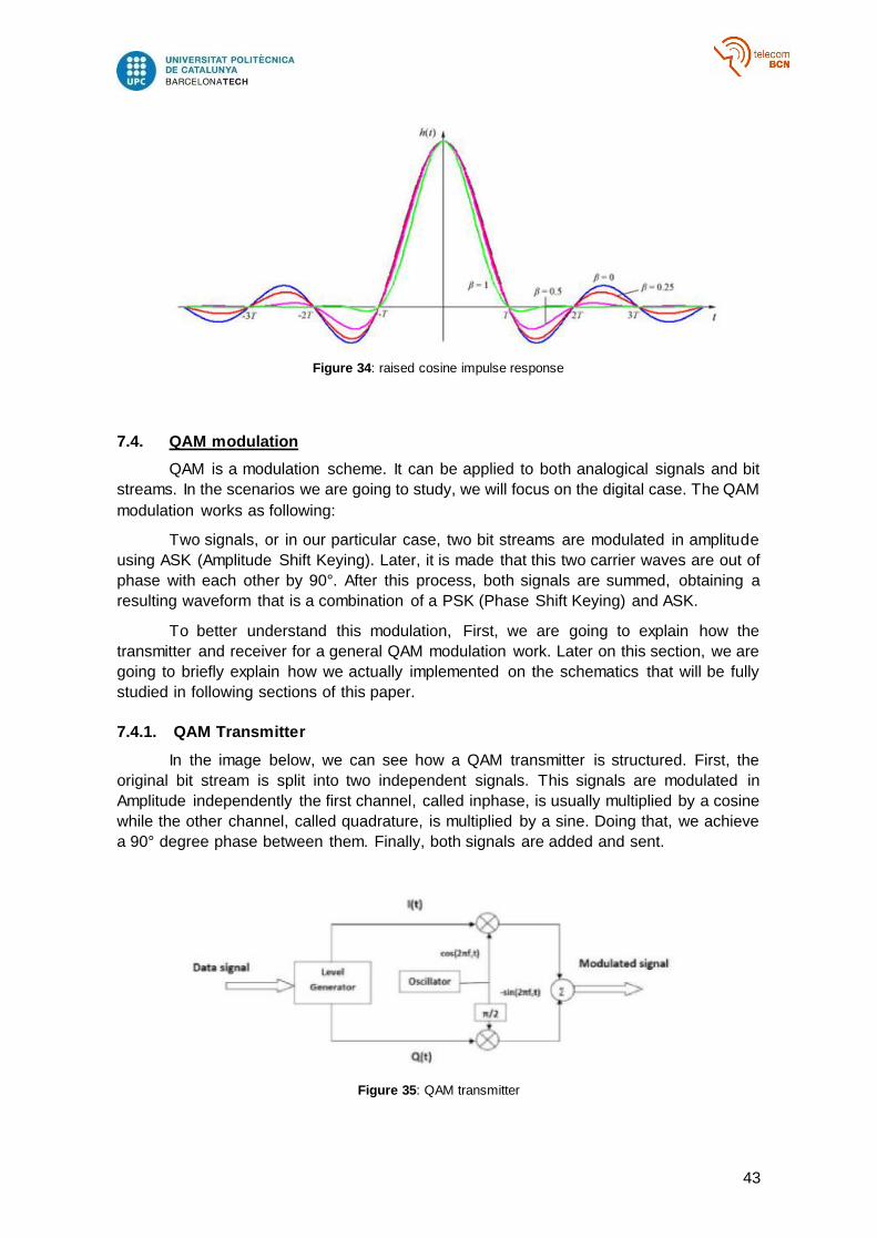
7.4. QAM modulation
QAM is a modulation scheme. It can be applied to both analogical signals and bit
streams. In the scenarios we are going to study, we will focus on the digital case. The QAM
modulation works as following:
Two signals, or in our particular case, two bit streams are modulated in amplitude
using ASK (Amplitude Shift Keying). Later, it is made that this two carrier waves are out of
phase with each other by 90°. After this process, both signals are summed, obtaining a
resulting waveform that is a combination of a PSK (Phase Shift Keying) and ASK.
To better understand this modulation, First, we are going to explain how the
transmitter and receiver for a general QAM modulation work. Later on this section, we are
going to briefly explain how we actually implemented on the schematics that will be fully
studied in following sections of this paper.
7.4.1. QAM Transmitter
In the image below, we can see how a QAM transmitter is structured. First, the
original bit stream is split into two independent signals. This signals are modulated in
Amplitude independently the first channel, called inphase, is usually multiplied by a cosine
while the other channel, called quadrature, is multiplied by a sine. Doing that, we achieve
a 90° degree phase between them. Finally, both signals are added and sent.
Figure 35: QAM transmitter
44
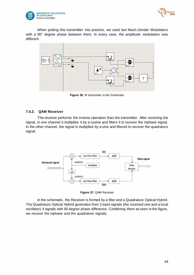
When putting this transmitter into practice, we used two Mach-Zender Modulators
with a 90° degree phase between them. In every case, the amplitude modulation was
different
Figure 36: M transmitter in the Schematic
7.4.2. QAM Receiver
The receiver performs the inverse operation than the transmitter. After receiving the
signal, in one channel it multiplies it by a cosine and filters it to recover the inphase signal.
In the other channel, the signal is multiplied by a sine and filtered to recover the quadrature
signal.
Figure 37: QAM Receiver
In the schematic, the Receiver is formed by a filter and a Quadrature Optical Hybrid.
The Quadrature Optical Hybrid generates from 2 input signals (the received one and a local
oscillator) 4 signals with 90 degree phase difference. Combining them as seen in the figure,
we recover the inphase and the quadrature signals.
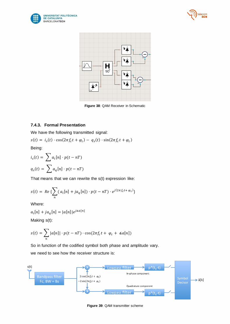
45 Figure 39: QAM transmitter scheme
Figure 38: QAM Receiver in Schematic
7.4.3. Formal Presentation
We have the following transmitted signal:
𝑠(𝑡) = 𝑖𝑠(𝑡) · cos(2𝜋𝑓𝑐𝑡 + 𝜑𝑐) − 𝑞𝑠(𝑡) · sin(2𝜋𝑓𝑐 𝑡 + 𝜑𝑐 )
Being:
𝑖𝑠(𝑡) = ∑ 𝑎𝑖 [𝑛] · 𝑝(𝑡 − 𝑛𝑇)
𝑞𝑠(𝑡) = ∑ 𝑎𝑞 [𝑛] · 𝑝(𝑡 − 𝑛𝑇)
That means that we can rewrite the s(t) expression like:
𝑠(𝑡) = 𝑅𝑒 {∑(
𝑛
𝑎𝑖[𝑛] + 𝑗𝑎𝑞 [𝑛]) · 𝑝(𝑡 − 𝑛𝑇) · 𝑒𝑗(2𝜋𝑓𝑐𝑡+ 𝜑𝑐)}
Where:
𝑎𝑖[𝑛] + 𝑗𝑎𝑞 [𝑛] = |𝑎[𝑛]|𝑒𝑗∡𝑎[𝑛]
Making s(t):
𝑠(𝑡) = ∑ |𝑎[𝑛]| · 𝑝(𝑡 − 𝑛𝑇) · cos (2𝜋𝑓𝑐 𝑡 + 𝜑𝑐 + ∡𝑎[𝑛])
𝑛
So in function of the codified symbol both phase and amplitude vary.
we need to see how the receiver structure is:
46
Figure 40: QAM receiver scheme
As perfectly seen in the above figure, the Coherent receiver allows us to recover both the
In-phase and Quadrature components so the symbol decision block can tell which was the
sent symbol every time â[k].
Next we need to know is how this receiver is generated optically, which can be seen in the
following figure:
Notice how the 0° and 180° outputs of the Hybrid are subtracted to obtain the In-phase
component at the exit of the photodiodes and the 90° and 270° outputs of the Hybrid are
subtracted to obtain the Quadrature component at the exit of the photodiodes.
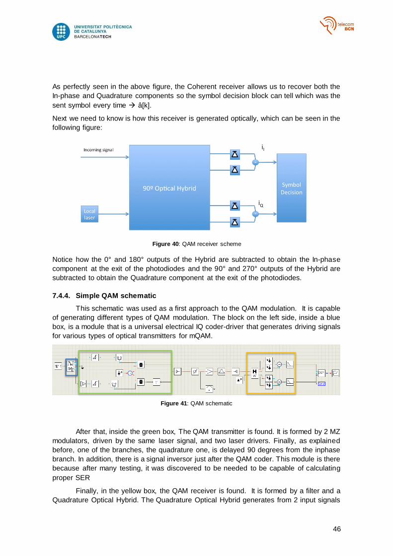
7.4.4. Simple QAM schematic
This schematic was used as a first approach to the QAM modulation. It is capable
of generating different types of QAM modulation. The block on the left side, inside a blue
box, is a module that is a universal electrical IQ coder-driver that generates driving signals
for various types of optical transmitters for mQAM.
Figure 41: QAM schematic
After that, inside the green box, The QAM transmitter is found. It is formed by 2 MZ
modulators, driven by the same laser signal, and two laser drivers. Finally, as explained
before, one of the branches, the quadrature one, is delayed 90 degrees from the inphase
branch. In addition, there is a signal inversor just after the QAM coder. This module is there
because after many testing, it was discovered to be needed to be capable of calculating
proper SER
Finally, in the yellow box, the QAM receiver is found. It is formed by a filter and a
Quadrature Optical Hybrid. The Quadrature Optical Hybrid generates from 2 input signals
47
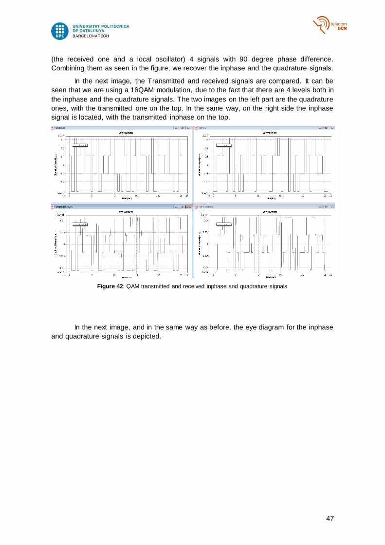
(the received one and a local oscillator) 4 signals with 90 degree phase difference.
Combining them as seen in the figure, we recover the inphase and the quadrature signals.
In the next image, the Transmitted and received signals are compared. It can be
seen that we are using a 16QAM modulation, due to the fact that there are 4 levels both in
the inphase and the quadrature signals. The two images on the left part are the quadrature
ones, with the transmitted one on the top. In the same way, on the right side the inphase
signal is located, with the transmitted inphase on the top.
Figure 42: QAM transmitted and received inphase and quadrature signals
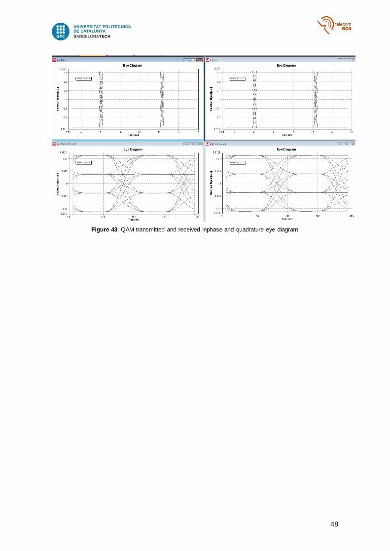
In the next image, and in the same way as before, the eye diagram for the inphase
and quadrature signals is depicted.
48
Figure 43: QAM transmitted and received inphase and quadrature eye diagram
49
Glossary
OTDM: Orthogonal Time Division Multiplexing
OFDM: Orthogonal Frequency Division Multiplexing
QAM: Quadrature Amplitude Modulation
ASK: Amplitude Shift Keying
PSK: Phase Shift Keying
ISI: Intersymbol Interference
BER: Bit Error Rate
SER: Symbol Error Rate