Embed Size (px)
Citation preview
Document Number: MC33PT2000Rev. 7.0, 9/2016
NXP Semiconductors Data sheet: Advance Information
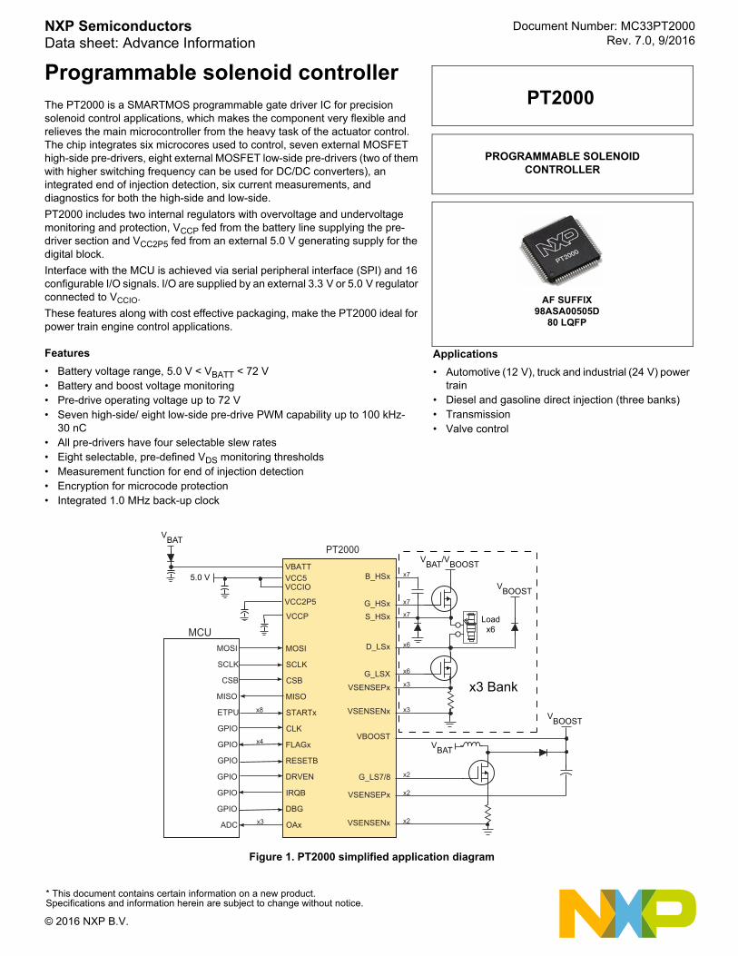
Programmable solenoid controllerThe PT2000 is a SMARTMOS programmable gate driver IC for precision solenoid control applications, which makes the component very flexible and relieves the main microcontroller from the heavy task of the actuator control. The chip integrates six microcores used to control, seven external MOSFET high-side pre-drivers, eight external MOSFET low-side pre-drivers (two of them with higher switching frequency can be used for DC/DC converters), an integrated end of injection detection, six current measurements, and diagnostics for both the high-side and low-side.
PT2000 includes two internal regulators with overvoltage and undervoltage monitoring and protection, VCCP fed from the battery line supplying the pre-driver section and VCC2P5 fed from an external 5.0 V generating supply for the digital block.
Interface with the MCU is achieved via serial peripheral interface (SPI) and 16 configurable I/O signals. I/O are supplied by an external 3.3 V or 5.0 V regulator connected to VCCIO.
These features along with cost effective packaging, make the PT2000 ideal for power train engine control applications.
Features
• Battery voltage range, 5.0 V < VBATT < 72 V• Battery and boost voltage monitoring• Pre-drive operating voltage up to 72 V• Seven high-side/ eight low-side pre-drive PWM capability up to 100 kHz-
30 nC• All pre-drivers have four selectable slew rates• Eight selectable, pre-defined VDS monitoring thresholds• Measurement function for end of injection detection• Encryption for microcode protection• Integrated 1.0 MHz back-up clock
Figure 1. PT2000 simplified application diagram
PROGRAMMABLE SOLENOID CONTROLLER
PT2000
AF SUFFIX98ASA00505D
80 LQFP
Applications
• Automotive (12 V), truck and industrial (24 V) power train
• Diesel and gasoline direct injection (three banks)• Transmission• Valve control
VBAT
VBAT/VBOOST
VBOOST
VBOOST
VBAT
5.0 V
Loadx6
x3 Bank
* This document contains certain information on a new product. Specifications and information herein are subject to change without notice.
© 2016 NXP B.V.

Table of Contents
1 Orderable parts . . . . . . . . . . . . . . . . . . . . . . . . . . . . . . . . . . . . . . . . . . . . . . . . . . . . . . . . . . . . . . . . . . . . . . . . . . . . . . . . . . . . . . 4
1.1 Cipher key . . . . . . . . . . . . . . . . . . . . . . . . . . . . . . . . . . . . . . . . . . . . . . . . . . . . . . . . . . . . . . . . . . . . . . . . . . . . . . . . . . . . . 4
2 Internal block diagram . . . . . . . . . . . . . . . . . . . . . . . . . . . . . . . . . . . . . . . . . . . . . . . . . . . . . . . . . . . . . . . . . . . . . . . . . . . . . . . . . 5
3 Pin connections . . . . . . . . . . . . . . . . . . . . . . . . . . . . . . . . . . . . . . . . . . . . . . . . . . . . . . . . . . . . . . . . . . . . . . . . . . . . . . . . . . . . . . 6
4 Functional description . . . . . . . . . . . . . . . . . . . . . . . . . . . . . . . . . . . . . . . . . . . . . . . . . . . . . . . . . . . . . . . . . . . . . . . . . . . . . . . . 10
4.1 Introduction . . . . . . . . . . . . . . . . . . . . . . . . . . . . . . . . . . . . . . . . . . . . . . . . . . . . . . . . . . . . . . . . . . . . . . . . . . . . . . . . . . . 10
4.2 Features . . . . . . . . . . . . . . . . . . . . . . . . . . . . . . . . . . . . . . . . . . . . . . . . . . . . . . . . . . . . . . . . . . . . . . . . . . . . . . . . . . . . . 10
5 Electrical characteristics . . . . . . . . . . . . . . . . . . . . . . . . . . . . . . . . . . . . . . . . . . . . . . . . . . . . . . . . . . . . . . . . . . . . . . . . . . . . . . 11
5.1 Maximum ratings . . . . . . . . . . . . . . . . . . . . . . . . . . . . . . . . . . . . . . . . . . . . . . . . . . . . . . . . . . . . . . . . . . . . . . . . . . . . . . . 11
5.2 Power supply electrical characteristics . . . . . . . . . . . . . . . . . . . . . . . . . . . . . . . . . . . . . . . . . . . . . . . . . . . . . . . . . . . . . . 13
5.3 High-side pre-driver electrical characteristics . . . . . . . . . . . . . . . . . . . . . . . . . . . . . . . . . . . . . . . . . . . . . . . . . . . . . . . . . 16
5.4 Low-side (LS1-LS6) pre-driver electrical characteristics . . . . . . . . . . . . . . . . . . . . . . . . . . . . . . . . . . . . . . . . . . . . . . . . . 17
5.5 Low-side high-speed (LS7-LS8) pre-driver electrical characteristics . . . . . . . . . . . . . . . . . . . . . . . . . . . . . . . . . . . . . . . . 19
5.6 High-side VDS VSRC monitoring electrical characteristics . . . . . . . . . . . . . . . . . . . . . . . . . . . . . . . . . . . . . . . . . . . . . . . 20
5.7 Low-side VDS VSRC monitoring electrical characteristics . . . . . . . . . . . . . . . . . . . . . . . . . . . . . . . . . . . . . . . . . . . . . . . 22
5.8 Load bias electrical characteristics . . . . . . . . . . . . . . . . . . . . . . . . . . . . . . . . . . . . . . . . . . . . . . . . . . . . . . . . . . . . . . . . . 23
5.9 Current measurement electrical characteristics . . . . . . . . . . . . . . . . . . . . . . . . . . . . . . . . . . . . . . . . . . . . . . . . . . . . . . . . 24
5.9.1 Current measurement for positive current . . . . . . . . . . . . . . . . . . . . . . . . . . . . . . . . . . . . . . . . . . . . . . . . . . . . . . . 24
5.9.2 Current measurement for negative currents . . . . . . . . . . . . . . . . . . . . . . . . . . . . . . . . . . . . . . . . . . . . . . . . . . . . . . 26
5.10 Analog output (OAx) electrical characteristics . . . . . . . . . . . . . . . . . . . . . . . . . . . . . . . . . . . . . . . . . . . . . . . . . . . . . . . . . 28
5.11 Clock / PLL electrical characteristics . . . . . . . . . . . . . . . . . . . . . . . . . . . . . . . . . . . . . . . . . . . . . . . . . . . . . . . . . . . . . . . . 29
5.12 Digital input/output electrical characteristics . . . . . . . . . . . . . . . . . . . . . . . . . . . . . . . . . . . . . . . . . . . . . . . . . . . . . . . . . . 30
5.13 Serial peripheral interface electrical characteristics . . . . . . . . . . . . . . . . . . . . . . . . . . . . . . . . . . . . . . . . . . . . . . . . . . . . . 32
6 Functional block description . . . . . . . . . . . . . . . . . . . . . . . . . . . . . . . . . . . . . . . . . . . . . . . . . . . . . . . . . . . . . . . . . . . . . . . . . . . 34
6.1 Power supplies . . . . . . . . . . . . . . . . . . . . . . . . . . . . . . . . . . . . . . . . . . . . . . . . . . . . . . . . . . . . . . . . . . . . . . . . . . . . . . . . 34
6.1.1 VCC5 . . . . . . . . . . . . . . . . . . . . . . . . . . . . . . . . . . . . . . . . . . . . . . . . . . . . . . . . . . . . . . . . . . . . . . . . . . . . . . . . . . . 34
6.1.2 VCCIO . . . . . . . . . . . . . . . . . . . . . . . . . . . . . . . . . . . . . . . . . . . . . . . . . . . . . . . . . . . . . . . . . . . . . . . . . . . . . . . . . . 34
6.1.3 VCC2P5 regulator . . . . . . . . . . . . . . . . . . . . . . . . . . . . . . . . . . . . . . . . . . . . . . . . . . . . . . . . . . . . . . . . . . . . . . . . . . 34
6.1.3 VCC2P5 regulator . . . . . . . . . . . . . . . . . . . . . . . . . . . . . . . . . . . . . . . . . . . . . . . . . . . . . . . . . . . . . . . . . . . . . . . . . . 34
6.1.4 VCCP regulator . . . . . . . . . . . . . . . . . . . . . . . . . . . . . . . . . . . . . . . . . . . . . . . . . . . . . . . . . . . . . . . . . . . . . . . . . . . . 35
6.1.5 Battery voltage monitor . . . . . . . . . . . . . . . . . . . . . . . . . . . . . . . . . . . . . . . . . . . . . . . . . . . . . . . . . . . . . . . . . . . . . . 36
6.1.6 Boost voltage monitor . . . . . . . . . . . . . . . . . . . . . . . . . . . . . . . . . . . . . . . . . . . . . . . . . . . . . . . . . . . . . . . . . . . . . . . 36
6.1.7 Charge pump . . . . . . . . . . . . . . . . . . . . . . . . . . . . . . . . . . . . . . . . . . . . . . . . . . . . . . . . . . . . . . . . . . . . . . . . . . . . . 38
6.2 Clock subsystem . . . . . . . . . . . . . . . . . . . . . . . . . . . . . . . . . . . . . . . . . . . . . . . . . . . . . . . . . . . . . . . . . . . . . . . . . . . . . . . 38
6.3 High-side pre-driver . . . . . . . . . . . . . . . . . . . . . . . . . . . . . . . . . . . . . . . . . . . . . . . . . . . . . . . . . . . . . . . . . . . . . . . . . . . . . 39
6.3.1 High-side pre-driver slew rate control . . . . . . . . . . . . . . . . . . . . . . . . . . . . . . . . . . . . . . . . . . . . . . . . . . . . . . . . . . . 40
6.3.2 Safe state of high-side pre-driver . . . . . . . . . . . . . . . . . . . . . . . . . . . . . . . . . . . . . . . . . . . . . . . . . . . . . . . . . . . . . . 40
6.4 High-side VDS and VSRC monitor . . . . . . . . . . . . . . . . . . . . . . . . . . . . . . . . . . . . . . . . . . . . . . . . . . . . . . . . . . . . . . . . . 42
6.4.1 HS1, 3, 5, 7 VDS monitoring . . . . . . . . . . . . . . . . . . . . . . . . . . . . . . . . . . . . . . . . . . . . . . . . . . . . . . . . . . . . . . . . . . 42
6.4.2 HS2, 4, 6 VDS monitoring . . . . . . . . . . . . . . . . . . . . . . . . . . . . . . . . . . . . . . . . . . . . . . . . . . . . . . . . . . . . . . . . . . . . 43
6.5 Low-side pre-driver (LS1-6) . . . . . . . . . . . . . . . . . . . . . . . . . . . . . . . . . . . . . . . . . . . . . . . . . . . . . . . . . . . . . . . . . . . . . . . 44
6.5.1 Low-side pre-driver slew rate control . . . . . . . . . . . . . . . . . . . . . . . . . . . . . . . . . . . . . . . . . . . . . . . . . . . . . . . . . . . 45
6.5.2 LS1 - LS6 VDS monitor . . . . . . . . . . . . . . . . . . . . . . . . . . . . . . . . . . . . . . . . . . . . . . . . . . . . . . . . . . . . . . . . . . . . . 46
6.6 Low-side pre-driver for DC/DC converter (LS7 and LS8) . . . . . . . . . . . . . . . . . . . . . . . . . . . . . . . . . . . . . . . . . . . . . . . . 47
6.6.1 Low-side pre-driver slew rate control (LS7 and LS8) . . . . . . . . . . . . . . . . . . . . . . . . . . . . . . . . . . . . . . . . . . . . . . . 48
6.6.2 Low-side VDS monitor D_ls7/D_ls8 for DC/DC . . . . . . . . . . . . . . . . . . . . . . . . . . . . . . . . . . . . . . . . . . . . . . . . . . . 48
NXP Semiconductors 2
PT2000
6.7 Current measurement . . . . . . . . . . . . . . . . . . . . . . . . . . . . . . . . . . . . . . . . . . . . . . . . . . . . . . . . . . . . . . . . . . . . . . . . . . . 49
6.7.1 General purpose current measurement block . . . . . . . . . . . . . . . . . . . . . . . . . . . . . . . . . . . . . . . . . . . . . . . . . . . . . 49
6.7.2 Current measurement for DC/DC . . . . . . . . . . . . . . . . . . . . . . . . . . . . . . . . . . . . . . . . . . . . . . . . . . . . . . . . . . . . . . 52
6.8 OA_x output pins, multiplexer and T & H . . . . . . . . . . . . . . . . . . . . . . . . . . . . . . . . . . . . . . . . . . . . . . . . . . . . . . . . . . . . . 53
6.8.1 General features . . . . . . . . . . . . . . . . . . . . . . . . . . . . . . . . . . . . . . . . . . . . . . . . . . . . . . . . . . . . . . . . . . . . . . . . . . . 53
6.8.2 OA_2 Pin digital I/O function . . . . . . . . . . . . . . . . . . . . . . . . . . . . . . . . . . . . . . . . . . . . . . . . . . . . . . . . . . . . . . . . . . 55
6.8.3 OAx output offset and offset error . . . . . . . . . . . . . . . . . . . . . . . . . . . . . . . . . . . . . . . . . . . . . . . . . . . . . . . . . . . . . . 56
7 Functional device operation . . . . . . . . . . . . . . . . . . . . . . . . . . . . . . . . . . . . . . . . . . . . . . . . . . . . . . . . . . . . . . . . . . . . . . . . . . . . 57
7.1 Power-up/down sequence . . . . . . . . . . . . . . . . . . . . . . . . . . . . . . . . . . . . . . . . . . . . . . . . . . . . . . . . . . . . . . . . . . . . . . . . 57
7.1.1 Power-up sequence of VCC5, VCC2P5, and reset . . . . . . . . . . . . . . . . . . . . . . . . . . . . . . . . . . . . . . . . . . . . . . . . . 57
7.1.2 Power-up sequence VCCP and bootstrap capacitors . . . . . . . . . . . . . . . . . . . . . . . . . . . . . . . . . . . . . . . . . . . . . . . 58
7.2 DC/DC converter control (LS7/8) . . . . . . . . . . . . . . . . . . . . . . . . . . . . . . . . . . . . . . . . . . . . . . . . . . . . . . . . . . . . . . . . . . . 61
7.2.1 General description . . . . . . . . . . . . . . . . . . . . . . . . . . . . . . . . . . . . . . . . . . . . . . . . . . . . . . . . . . . . . . . . . . . . . . . . . 61
7.3 Device clock manager and PLL init . . . . . . . . . . . . . . . . . . . . . . . . . . . . . . . . . . . . . . . . . . . . . . . . . . . . . . . . . . . . . . . . . 63
7.4 SW initialization flow . . . . . . . . . . . . . . . . . . . . . . . . . . . . . . . . . . . . . . . . . . . . . . . . . . . . . . . . . . . . . . . . . . . . . . . . . . . . 63
7.4.1 Power supply, reset, and clock . . . . . . . . . . . . . . . . . . . . . . . . . . . . . . . . . . . . . . . . . . . . . . . . . . . . . . . . . . . . . . . . 63
7.4.2 SPI configuration . . . . . . . . . . . . . . . . . . . . . . . . . . . . . . . . . . . . . . . . . . . . . . . . . . . . . . . . . . . . . . . . . . . . . . . . . . . 64
7.4.3 Clock monitor, flash enable, and DrvEn . . . . . . . . . . . . . . . . . . . . . . . . . . . . . . . . . . . . . . . . . . . . . . . . . . . . . . . . . 64
7.5 BIST . . . . . . . . . . . . . . . . . . . . . . . . . . . . . . . . . . . . . . . . . . . . . . . . . . . . . . . . . . . . . . . . . . . . . . . . . . . . . . . . . . . . . . . . . 64
7.5.1 MBIST . . . . . . . . . . . . . . . . . . . . . . . . . . . . . . . . . . . . . . . . . . . . . . . . . . . . . . . . . . . . . . . . . . . . . . . . . . . . . . . . . . . 65
7.5.2 LBIST . . . . . . . . . . . . . . . . . . . . . . . . . . . . . . . . . . . . . . . . . . . . . . . . . . . . . . . . . . . . . . . . . . . . . . . . . . . . . . . . . . . 65
7.6 Reset sources . . . . . . . . . . . . . . . . . . . . . . . . . . . . . . . . . . . . . . . . . . . . . . . . . . . . . . . . . . . . . . . . . . . . . . . . . . . . . . . . . 65
7.7 Cipher unit . . . . . . . . . . . . . . . . . . . . . . . . . . . . . . . . . . . . . . . . . . . . . . . . . . . . . . . . . . . . . . . . . . . . . . . . . . . . . . . . . . . . 66
7.8 Ground connections . . . . . . . . . . . . . . . . . . . . . . . . . . . . . . . . . . . . . . . . . . . . . . . . . . . . . . . . . . . . . . . . . . . . . . . . . . . . . 66
7.9 Shutoff path via the DrvEn pin . . . . . . . . . . . . . . . . . . . . . . . . . . . . . . . . . . . . . . . . . . . . . . . . . . . . . . . . . . . . . . . . . . . . . 66
8 Digital core . . . . . . . . . . . . . . . . . . . . . . . . . . . . . . . . . . . . . . . . . . . . . . . . . . . . . . . . . . . . . . . . . . . . . . . . . . . . . . . . . . . . . . . . . 68
8.1 Logic channels description . . . . . . . . . . . . . . . . . . . . . . . . . . . . . . . . . . . . . . . . . . . . . . . . . . . . . . . . . . . . . . . . . . . . . . . . 68
8.1.1 Microcores . . . . . . . . . . . . . . . . . . . . . . . . . . . . . . . . . . . . . . . . . . . . . . . . . . . . . . . . . . . . . . . . . . . . . . . . . . . . . . . . 69
8.1.2 Dual microcore arbiter . . . . . . . . . . . . . . . . . . . . . . . . . . . . . . . . . . . . . . . . . . . . . . . . . . . . . . . . . . . . . . . . . . . . . . . 70
8.1.3 Signature unit . . . . . . . . . . . . . . . . . . . . . . . . . . . . . . . . . . . . . . . . . . . . . . . . . . . . . . . . . . . . . . . . . . . . . . . . . . . . . 72
8.1.4 SPI backdoor . . . . . . . . . . . . . . . . . . . . . . . . . . . . . . . . . . . . . . . . . . . . . . . . . . . . . . . . . . . . . . . . . . . . . . . . . . . . . . 72
8.1.5 CRAM . . . . . . . . . . . . . . . . . . . . . . . . . . . . . . . . . . . . . . . . . . . . . . . . . . . . . . . . . . . . . . . . . . . . . . . . . . . . . . . . . . . 73
8.1.6 DRAM . . . . . . . . . . . . . . . . . . . . . . . . . . . . . . . . . . . . . . . . . . . . . . . . . . . . . . . . . . . . . . . . . . . . . . . . . . . . . . . . . . . 73
8.2 Serial peripheral interface . . . . . . . . . . . . . . . . . . . . . . . . . . . . . . . . . . . . . . . . . . . . . . . . . . . . . . . . . . . . . . . . . . . . . . . . 74
8.2.1 SPI read access . . . . . . . . . . . . . . . . . . . . . . . . . . . . . . . . . . . . . . . . . . . . . . . . . . . . . . . . . . . . . . . . . . . . . . . . . . . 75
8.2.2 SPI write access . . . . . . . . . . . . . . . . . . . . . . . . . . . . . . . . . . . . . . . . . . . . . . . . . . . . . . . . . . . . . . . . . . . . . . . . . . . 76
8.2.3 SPI protocol . . . . . . . . . . . . . . . . . . . . . . . . . . . . . . . . . . . . . . . . . . . . . . . . . . . . . . . . . . . . . . . . . . . . . . . . . . . . . . . 77
8.3 SPI address map . . . . . . . . . . . . . . . . . . . . . . . . . . . . . . . . . . . . . . . . . . . . . . . . . . . . . . . . . . . . . . . . . . . . . . . . . . . . . . . 79
8.3.1 Selection register (3FFh) . . . . . . . . . . . . . . . . . . . . . . . . . . . . . . . . . . . . . . . . . . . . . . . . . . . . . . . . . . . . . . . . . . . . . 89
8.3.2 Configuration register . . . . . . . . . . . . . . . . . . . . . . . . . . . . . . . . . . . . . . . . . . . . . . . . . . . . . . . . . . . . . . . . . . . . . . . 90
8.3.3 IO configuration registers . . . . . . . . . . . . . . . . . . . . . . . . . . . . . . . . . . . . . . . . . . . . . . . . . . . . . . . . . . . . . . . . . . . 100
8.3.4 Main configuration registers . . . . . . . . . . . . . . . . . . . . . . . . . . . . . . . . . . . . . . . . . . . . . . . . . . . . . . . . . . . . . . . . . 117
8.3.5 Diagnostics configuration registers . . . . . . . . . . . . . . . . . . . . . . . . . . . . . . . . . . . . . . . . . . . . . . . . . . . . . . . . . . . . 132
9 Typical applications . . . . . . . . . . . . . . . . . . . . . . . . . . . . . . . . . . . . . . . . . . . . . . . . . . . . . . . . . . . . . . . . . . . . . . . . . . . . . . . . . 139
9.1 Application diagram: 3 bank, 6 cylinder with DC/DC . . . . . . . . . . . . . . . . . . . . . . . . . . . . . . . . . . . . . . . . . . . . . . . . . . . 139
9.2 Application diagram: 3 bank, 3 cylinder (full overlap) with DC/DC . . . . . . . . . . . . . . . . . . . . . . . . . . . . . . . . . . . . . . . . . 140
10 Packaging . . . . . . . . . . . . . . . . . . . . . . . . . . . . . . . . . . . . . . . . . . . . . . . . . . . . . . . . . . . . . . . . . . . . . . . . . . . . . . . . . . . . . . . . . 141
10.1 Package mechanical dimensions . . . . . . . . . . . . . . . . . . . . . . . . . . . . . . . . . . . . . . . . . . . . . . . . . . . . . . . . . . . . . . . . . . 141
11 Reference section . . . . . . . . . . . . . . . . . . . . . . . . . . . . . . . . . . . . . . . . . . . . . . . . . . . . . . . . . . . . . . . . . . . . . . . . . . . . . . . . . . 145
12 Revision history . . . . . . . . . . . . . . . . . . . . . . . . . . . . . . . . . . . . . . . . . . . . . . . . . . . . . . . . . . . . . . . . . . . . . . . . . . . . . . . . . . . . 146
3 NXP Semiconductors
PT2000
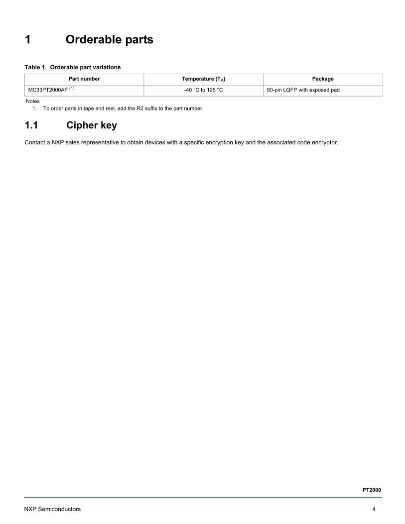
1 Orderable parts
1.1 Cipher key
Contact a NXP sales representative to obtain devices with a specific encryption key and the associated code encryptor.
Table 1. Orderable part variations
Part number Temperature (TA) Package
MC33PT2000AF (1) -40 °C to 125 °C 80-pin LQFP with exposed pad
Notes1. To order parts in tape and reel, add the R2 suffix to the part number.
NXP Semiconductors 4
PT2000
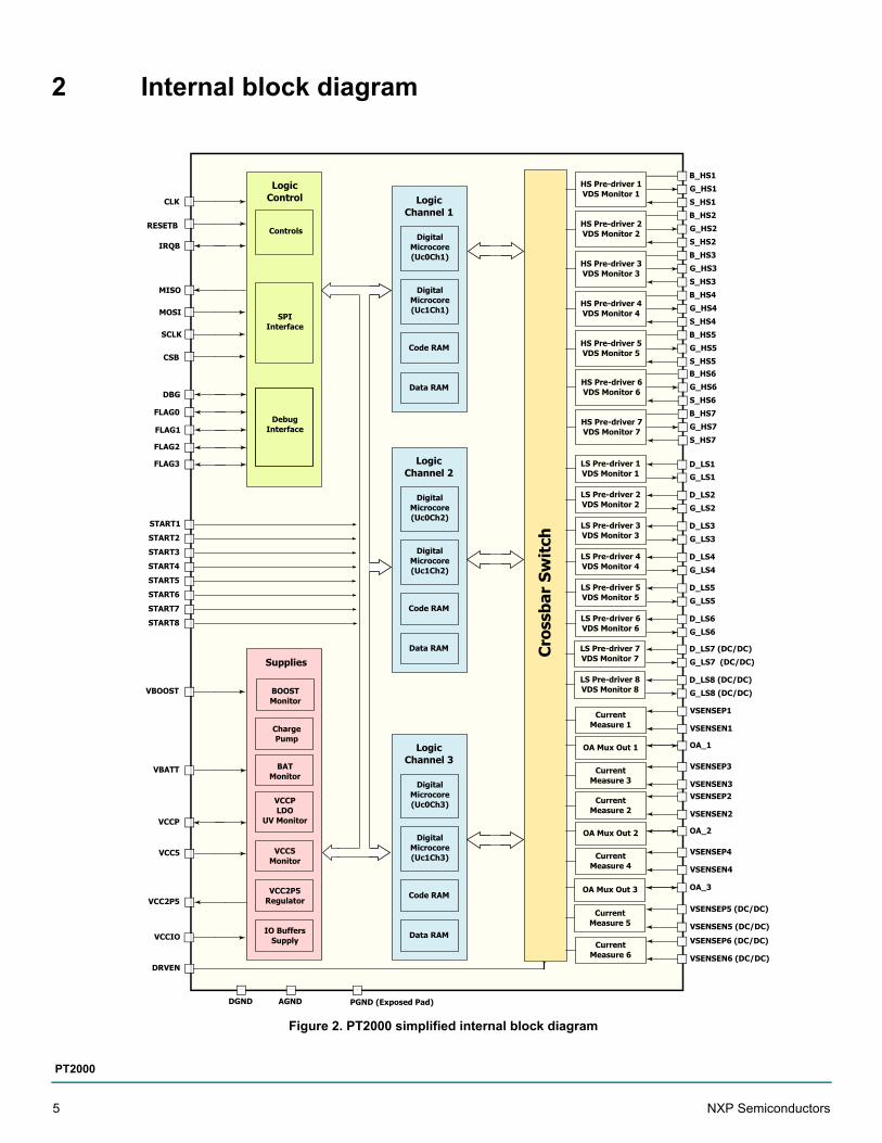
2 Internal block diagram
Figure 2. PT2000 simplified internal block diagram
CLK
RESETB
IRQB
MISO
MOSI
SCLK
CSB
DBG
FLAG0
FLAG1
FLAG2
START1
START2
START3
START4
START5
START6
VBOOST
VBATT
VCCP
VCC5
VCC2P5
VCCIO
DRVEN
Logic Control
Controls
SPI Interface
Debug Interface
BAT Monitor
Charge Pump
VCCPLDO
UV Monitor
IO Buffers Supply
VCC5 Monitor
VCC2P5 Regulator
LogicChannel 1
Digital Microcore(Uc0Ch1)
Code RAM
Digital Microcore(Uc1Ch1)
Data RAM
LogicChannel 3
Digital Microcore(Uc0Ch3)
Code RAM
Digital Microcore(Uc1Ch3)
Data RAM
AGND PGND (Exposed Pad)
Cro
ssba
r Sw
itch
HS Pre-driver 1VDS Monitor 1
G_HS1
B_HS1
S_HS1
HS Pre-driver 2VDS Monitor 2
G_HS2
B_HS2
S_HS2
HS Pre-driver 3VDS Monitor 3
G_HS3
B_HS3
S_HS3
HS Pre-driver 4VDS Monitor 4
G_HS4
B_HS4
S_HS4
HS Pre-driver 5VDS Monitor 5
G_HS5
B_HS5
S_HS5
LS Pre-driver 1VDS Monitor 1 G_LS1
D_LS1
LS Pre-driver 2VDS Monitor 2 G_LS2
D_LS2
LS Pre-driver 3VDS Monitor 3 G_LS3
D_LS3
LS Pre-driver 4VDS Monitor 4 G_LS4
D_LS4
LS Pre-driver 5VDS Monitor 5 G_LS5
D_LS5
LS Pre-driver 6VDS Monitor 6 G_LS6
D_LS6
Current Measure 1
VSENSEP1
VSENSEN1
OA Mux Out 1 OA_1
Current Measure 3
VSENSEP3
VSENSEN3
Current Measure 2
VSENSEP2
VSENSEN2
Current Measure 4
VSENSEP4
VSENSEN4
OA Mux Out 2 OA_2
LogicChannel 2
Digital Microcore(Uc0Ch2)
Code RAM
Digital Microcore(Uc1Ch2)
Data RAM
HS Pre-driver 6VDS Monitor 6
G_HS6
B_HS6
S_HS6
HS Pre-driver 7VDS Monitor 7
G_HS7
B_HS7
S_HS7
LS Pre-driver 7VDS Monitor 7 G_LS7 (DC/DC)
D_LS7 (DC/DC)
LS Pre-driver 8VDS Monitor 8 G_LS8 (DC/DC)
D_LS8 (DC/DC)
Current Measure 5
VSENSEP5 (DC/DC)
VSENSEN5 (DC/DC)
OA Mux Out 3 OA_3
Current Measure 6
VSENSEP6 (DC/DC)
VSENSEN6 (DC/DC)
START7
START8
Supplies
FLAG3
DGND
BOOST Monitor
5 NXP Semiconductors
PT2000
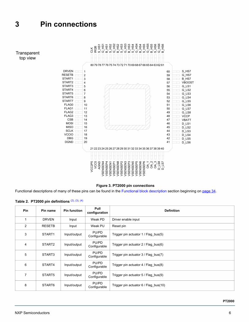
3 Pin connections
Figure 3. PT2000 pin connections
Functional descriptions of many of these pins can be found in the Functional block description section beginning on page 34.
Table 2. PT2000 pin definitions (2), (3), (4)
Pin Pin name Pin functionPull
configurationDefinition
1 DRVEN Input Weak PD Driver enable input
2 RESETB Input Weak PU Reset pin
3 START1 Input/outputPU/PD
ConfigurableTrigger pin actuator 1 / Flag_bus(5)
4 START2 Input/outputPU/PD
ConfigurableTrigger pin actuator 2 / Flag_bus(6)
5 START3 Input/outputPU/PD
ConfigurableTrigger pin actuator 3 / Flag_bus(7)
6 START4 Input/outputPU/PD
ConfigurableTrigger pin actuator 4 / Flag_bus(8)
7 START5 Input/outputPU/PD
ConfigurableTrigger pin actuator 5 / Flag_bus(9)
8 START6 Input/outputPU/PD
ConfigurableTrigger pin actuator 6 / Flag_bus(10)
Transparenttop view
1234567891011121314151617181920
21 22 23 24 25 26 27 28 29 30 31 32 33 34 35 36 37 38 39 40
4142434445464748495051525354555657585960
6162636465666768697071727374757677787980
DRVENRESETBSTART1START2START3START4START5START6START7
FLAG0FLAG1FLAG2FLAG3
CSBMOSIMISOSCLK
VCCIODBG
DGND
VC
C2P
5V
CC
5A
GN
DV
SE
NS
EN
4V
SE
NS
EP
4V
SE
NS
EN
1V
SE
NS
EP
1V
SE
NS
EN
8V
SE
NS
EP
2V
SE
NS
EN
3V
SE
NS
EP
3V
SE
NS
EN
5V
SE
NS
EP
5V
SE
NS
EN
6V
SE
NS
EP
6O
A_1
OA
_2
OA
_3
D_L
S8
D_L
S7
S_HS7G_HS7B_HS7VBOOSTG_LS1G_LS2G_LS3G_LS4G_LS5G_LS6G_LS7G_LS8VCCPVBATTD_LS1D_LS2D_LS3D_LS4D_LS5D_LS6
CLK
IRQ
BS
_HS
1G
_HS
1B
_HS
1S
_HS
2
S_H
S3
G_H
S3
B_H
S3
S_H
S4
G_H
S4
B_H
S4
S_H
S5
G_H
S5
B_H
S5
S_H
S6
G_H
S6
B_H
S6
G_H
S2
B_H
S2
NXP Semiconductors 6
PT2000
9 START7 Input/outputPU/PD
ConfigurableTrigger pin actuator 7 / Flag_bus(11)
10 FLAG 0 Input/output Weak PDFlag_bus(0) (general purpose I/O)/command for external free-wheeling MOSFTET pre-driver 1
11 FLAG 1 Input/output Weak PDFlag_bus(1) (general purpose I/O)/command for external free-wheeling MOSFTET pre-driver 2
12 FLAG 2 Input/output Weak PDFlag_bus(2) (general purpose I/O)/command for external free-wheeling MOSFTET pre-driver 3
13 FLAG 3 Input/output Weak PDFlag_bus(3) (general purpose I/O)/command for external free-wheeling MOSFTET pre-driver 4
14 CSB Input PU SPI chip select
15 MOSI Input Weak PU SPI slave input
16 MISO Output — SPI slave output
17 SCLK Input Weak PU SPI clock
18 VCCIO Input — Digital I/O voltage supply 3.3 V or 5.0 V (supplied externally)
19 DBG Input/output Weak PU Debug port / Flag_bus (15)
20 DGND Ground — Digital ground
21 VCC2P5 Output — Internal 2.5 V voltage regulator decoupling
22 VCC5 Input — Power supply 5.0 V (supplied externally)
23 AGND Ground — Analog ground
24 VSENSEN4 Input/outputPU/PD
ConfigurableCurrent sense input comparator - / Start8 / Flag(12)
25 VSENSEP4 Input/output Weak PD Current sense input comparator + /Flag(4) (general purpose I/O)
26 VSENSEN1 Input — Current sense input comparator 1 -
27 VSENSEP1 Input — Current sense input comparator 1 +
28 VSENSEN2 Input — Current sense input comparator 2 -
29 VSENSEP2 Input — Current sense input comparator 2 +
30 VSENSEN3 Input — Current sense input comparator 3 -
31 VSENSEP3 Input — Current sense input comparator 3 +
32 VSENSEN5 Input — DC-DC current sense input comparator -
33 VSENSEP5 Input — DC-DC current sense input comparator +
34 VSENSEN6 Input — DC-DC current sense input comparator -
35 VSENSEP6 Input — DC-DC current sense input comparator +
36 OA_1 Output — Analog output 1
37 OA_2 Input/output Weak PD Analog output 2/Flag_bus (14)
38 OA_3 Output — Analog output 3
39 D_LS8 Input — Drain pin low-side MOSFET for DC/DC converter
40 D_LS7 Input — Drain pin low-side MOSFET for DC/DC converter
41 D_LS6 Input — Drain pin low-side MOSFET actuator 6
42 D_LS5 Input — Drain pin low-side MOSFET actuator 5
43 D_LS4 Input — Drain pin low-side MOSFET actuator 4
Table 2. PT2000 pin definitions (2), (3), (4)(continued)
Pin Pin name Pin functionPull
configurationDefinition
7 NXP Semiconductors
PT2000
44 D_LS3 Input — Drain pin low-side MOSFET actuator 3
45 D_LS2 Input — Drain pin low-side MOSFET actuator 2
46 D_LS1 Input — Drain pin low-side MOSFET actuator 1
47 VBATT Input — Battery voltage input
48 VCCP Input/output —Output: Internal 7.0 V voltage regulatorInput: External 7.0 V voltage regulator (supplied externally)
49 G_LS8 Output — Gate pin low-side high speed MOSFET can be used for DC/DC converter
50 G_LS7 Output — Gate pin low-side high speed MOSFET can be used for DC/DC converter
51 G_LS6 Output — Gate pin low-side MOSFET actuator 6
52 G_LS5 Output — Gate pin low-side MOSFET actuator 5
53 G_LS4 Output — Gate pin low-side MOSFET actuator 4
54 G_LS3 Output — Gate pin low-side MOSFET actuator 3
55 G_LS2 Output — Gate pin low-side MOSFET actuator 2
56 G_LS1 Output — Gate pin low-side MOSFET actuator 1
57 VBOOST Input — Boost voltage and drain pin for boost pre-drivers
58 B_HS7 - — Bootstrap pin high-side MOSFET 7
59 G_HS7 Output — Gate pin high-side MOSFET 7
60 S_HS7 Input — Source pin high side MOSFET 7
61 B_HS6 - — Bootstrap pin Boost MOSFET 6
62 G_HS6 Output — Gate pin Boost MOSFET 6
63 S_HS6 Input — Source pin Boost MOSFET 6
64 B_HS5 - — Bootstrap pin high-side MOSFET 5
65 G_HS5 Output — Gate pin high-side MOSFET 5
66 S_HS5 Input — Source pin high side MOSFET 5
67 B_HS4 - — Bootstrap pin boost MOSFET 4
68 G_HS4 Output — Gate pin boost MOSFET 4
69 S_HS4 Input — Source pin boost MOSFET 4
70 B_HS3 - — Bootstrap pin high-side MOSFET 3
71 G_HS3 Output — Gate pin high-side MOSFET 3
72 S_HS3 Input — Source pin high-side MOSFET 3
73 B_HS2 - — Bootstrap pin boost MOSFET 2
74 G_HS2 Output — Gate pin boost MOSFET 2
75 S_HS2 Input — Source pin boost MOSFET 2
76 B_HS1 - — Bootstrap pin high-side MOSFET 1
77 G_HS1 Output — Gate pin high-side MOSFET 1
78 S_HS1 Input — Source pin high-side MOSFET 1
79 IRQB Input/output Weak PD Interrupt output/Flag_bus (13)
80 CLK Input Weak PU Clock pin (low-frequency reference for internal PLL)
Table 2. PT2000 pin definitions (2), (3), (4)(continued)
Pin Pin name Pin functionPull
configurationDefinition
NXP Semiconductors 8
PT2000
ePAD PGND Ground — Power ground (to be soldered on GND PCB)
Notes2. External 7.0 V is required in case the typical battery voltage is 24 V (See External VCCP (vccp_ext_en='1') on page 35).3. Except for supply and ground, it is guaranteed by design unused pins can be kept open without any impact on the device.4. Unused VSENSEPx and VSENSEx pins can both be connected to GND.
Table 3. Resistor types
Pin type Description
PU Pull-up to VCCIO (nominal value: 120 kΩ)
Weak PU Weak pull-up to VCCIO (nominal value: 480 kΩ)
PD Pull-down to AGND (nominal value: 120 kΩ)
Weak PD Weak pull-down to AGND (nominal value: 480 kΩ)
Table 2. PT2000 pin definitions (2), (3), (4)(continued)
Pin Pin name Pin functionPull
configurationDefinition
9 NXP Semiconductors
PT2000
4 Functional description
4.1 Introduction
The PT2000 is a mixed signal IC for engine injector and electrical valve control, which provides a cost effective, flexible, and smart, high-side and low-side MOSFET gate driver. The device includes both individual charge pump outputs for each high-side pre-driver and high-voltage DC/DC converter pre-driver. Gate drive, diagnostics, and protection against external faults, are managed through six independent and concurrent digital microcores. Each of the three logic channels including two microcores and their own code RAM and data RAM. The internal microcode is protected against theft via encryption and corruption via check sums. Those microcores are optimized to control power MOSFET with a small latency time. The PT2000 can control three banks of two injectors each or three banks with one injector per bank for full overlap,
4.2 Features
High-side and low-side pre-drivers
• Seven high-side pre-drivers for logic level N-channel MOSFETs using four programmable slew rates• Six low-side pre-drivers for logic level N-channel MOSFETs using four programmable slew rates• Integrated bootstrap circuitry for each high-side pre-driver• Integrated charge pump circuitry for each high-side pre-driver with 100% duty cycle capability• Configurable automatic freewheeling capability between high-side and low-side
DC/DC converter
• Two low-side pre-driver, for a logic level N-channel MOSFET, can be optionally dedicated to providing a boost DC-DC converter with four programmable slew rates
• Three different control modes to reduce power dissipation (manual, hysteretic, resonant)
Current measurement
• Four independent current measurement blocks• Two current measurements (channel 5 and 6) are optionally configurable to support DC/DC converters
Diagnostics and monitoring
• VDS and VSRC monitoring (programmable values) for fault protection and diagnostics• VBOOST monitoring• VBAT monitoring• Temperature monitoring
Integrated end of injection detection
• Accurate detection of end of injection for each high-side source and low-side drain without any external component needed.
Power supplies
• Integrated 7.0 V linear regulator (VCCP) for the HS/LS gate power supply (2)
• Integrated 2.5 V linear regulator (VCC2P5) for the digital core supply based on the VCC5 input supply• External 5.0 V supply (VCC5) • Selectable VCCIO external supply (5.0 V or 3.3 V) for digital I/O
Digital block
• Six digital microcores, each with their own ALU, and full access to the system crossbar switch• Three memory banks: 1024 x 16-bit of code RAM with built-in error detection and 64 x 16-bit of data RAM• Memory BIST and Logic BIST activated by the SPI, with pass/fail status
Control interface
• 16-bit slave SPI up to 10 MHz - two protocols - programmable slew rate• 16 general purpose digital IOs able to sustain up to 36 V• Independent direct pre-driver inhibition input for safety purposes
NXP Semiconductors 10
PT2000
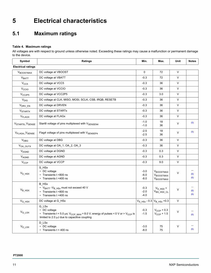
5 Electrical characteristics
5.1 Maximum ratings
Table 4. Maximum ratings
All voltages are with respect to ground unless otherwise noted. Exceeding these ratings may cause a malfunction or permanent damage to the device.
Symbol Ratings Min. Max. Unit Notes
Electrical ratings
VBOOSTMAX DC voltage at VBOOST 0 72 V
VBATT DC voltage at VBATT -0.3 72 V
VCC5 DC voltage at VCC5 -0.3 36 V
VCCIO DC voltage at VCCIO -0.3 36 V
VCC2P5 DC voltage at VCC2P5 -0.3 3.0 V
VDIG DC voltage at CLK, MISO, MOSI, SCLK, CSB, IRQB, RESETB -0.3 36 V
VDRV_EN DC voltage at DRVEN -0.3 36 V
VSTARTX DC voltage at STARTx -0.3 36 V
VFLAGX DC voltage at FLAGx -0.3 36 V
VSTART8_VSENSE Start8 voltage of pins multiplexed with VSENSEN4-1.0-1.0
1836
V (5)
VFLAG4_VSENSE Flag4 voltage of pins multiplexed with VSENSEP4-2.5-2.5
1836
V (5)
VDBG DC voltage at DBG -0.3 36 V
VOA_OUTX DC voltage at OA_1, OA_2, OA_3 -0.3 36 V
VDGND DC voltage at DGND -0.3 0.3 V
VAGND DC voltage at AGND -0.3 0.3 V
VCCP DC voltage at VCCP -0.3 9.0 V
VS_HSX
S_HSx• DC voltage• Transients t <800 ns• Transients t <400 ns
-3.0-6.0-8.0
VBOOSTMAXVBOOSTMAXVBOOSTMAX
V—
(6)
(6)
VB_HSX
B_HSx• VBATT -VB_HSx must not exceed 40 V
• Transients t <800 ns• Transients t <400 ns
-0.3-2.0-4.0
VS_HSX + VBS_HSX_CL
V—
(6)
(6)
VG_HSX DC voltage at G_HSx VS_HSx - 0.3 VB_HSx +0.3 V
VG_LSX
G_LSx• DC voltage• Transients t < 5.0 μs; VCCP_MAX = 8.0 V; energy of pulses < 0 V or > VCCP is limited to 2.0 μJ due to capacitive coupling
-0.3-1.5
VCCP + 0.3VCCP + 1.5
V —
(6)
VD_LSX
D_LSx • DC voltage• Transients t < 400 ns
-3.0-8.0
7575
V —
(6)
11 NXP Semiconductors
PT2000
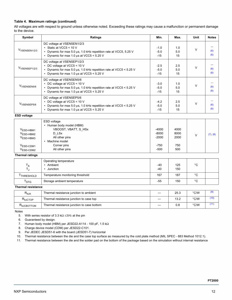
VVSENSEN1/2/3
DC voltage at VSENSEN1/2/3• Static at VCC5 < 10 V • Dynamic for max 5.0 μs, 1.0 kHz repetition rate at VCC5, 5.25 V• Dynamic for max 1.0 μs at VCC5 < 5.25 V
-1.0-5.0-15
1.05.015
V—
(6)
(6)
VVSENSEP1/2/3
DC voltage at VSENSEP1/2/3• DC voltage at VCC5 < 10 V • Dynamic for max 5.0 μs, 1.0 kHz repetition rate at VCC5 < 5.25 V• Dynamic for max 1.0 μs at VCC5 < 5.25 V
-2.5-5.0-15
2.55.015
V—
(6)
(6)
VVSENSEN5/6
DC voltage at VSENSEN5/6• DC voltage at VCC5 < 10 V • Dynamic for max 5.0 μs, 1.0 kHz repetition rate at VCC5 < 5.25 V• Dynamic for max 1.0 μs at VCC5 < 5.25 V
-3.0-5.0-15
1.05.015
V—
(6)
(6)
VVSENSEP5/6
DC voltage at VSENSEP5/6• DC voltage at VCC5 < 10 V • Dynamic for max 5.0 μs, 1.0 kHz repetition rate at VCC5 < 5.25 V• Dynamic for max 1.0 μs at VCC5 < 5.25 V
-4.2-5.0-15
2.55.015
V—
(6)
(6)
ESD voltage
VESD-HBM1VESD-HBM2VESD-HBM3
VESD-CDM1VESD-CDM2
ESD voltage• Human body model (HBM)
VBOOST, VBATT, S_HSxD_LSxAll other pins
• Machine modelCorner pinsAll other pins
-4000-8000-2000
-750-500
400080002000
750500
V (7), (8)
Thermal ratings
TATJ
Operating temperature • Ambient• Junction
- 40-40
125150
°C
TTHRESHOLD Temperature monitoring threshold 167 187 °C
TSTG Storage ambient temperature -55 150 °C
Thermal resistance
RθJA Thermal resistance junction to ambient — 25.3 °C/W (9)
RθJCTOP Thermal resistance junction to case top — 13.2 °C/W (10)
RθJCBOTTOM Thermal resistance junction to case bottom — 0.8 °C/W (11)
Notes5. With series resistor of 3.3 kΩ ±20% at the pin6. Guaranteed by design.7. Human body model (HBM) per JESD22-A114 - 100 pF, 1.5 kΩ8. Charge device model (CDM) per JESD22-C101.9. Per JEDEC JESD51-6 with the board (JESD51-7) horizontal
10. Thermal resistance between the die and the case top surface as measured by the cold plate method (MIL SPEC - 883 Method 1012.1).11. Thermal resistance between the die and the solder pad on the bottom of the package based on the simulation without internal resistance
Table 4. Maximum ratings (continued)
All voltages are with respect to ground unless otherwise noted. Exceeding these ratings may cause a malfunction or permanent damage to the device.
Symbol Ratings Min. Max. Unit Notes
NXP Semiconductors 12
PT2000
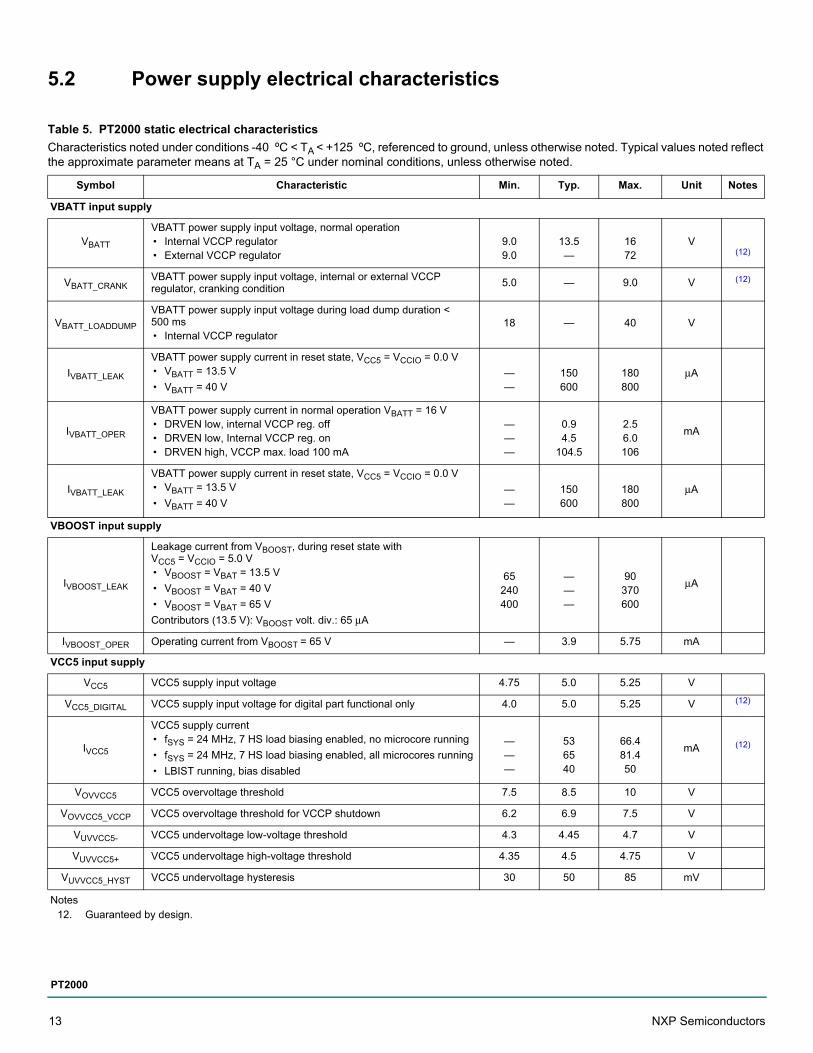
5.2 Power supply electrical characteristics
Table 5. PT2000 static electrical characteristics
Characteristics noted under conditions -40 ºC < TA < +125 ºC, referenced to ground, unless otherwise noted. Typical values noted reflect the approximate parameter means at TA = 25 °C under nominal conditions, unless otherwise noted.
Symbol Characteristic Min. Typ. Max. Unit Notes
VBATT input supply
VBATT
VBATT power supply input voltage, normal operation• Internal VCCP regulator• External VCCP regulator
9.09.0
13.5—
1672
V(12)
VBATT_CRANKVBATT power supply input voltage, internal or external VCCP regulator, cranking condition
5.0 — 9.0 V (12)
VBATT_LOADDUMP
VBATT power supply input voltage during load dump duration < 500 ms• Internal VCCP regulator
18 — 40 V
IVBATT_LEAK
VBATT power supply current in reset state, VCC5 = VCCIO = 0.0 V• VBATT = 13.5 V
• VBATT = 40 V——
150600
180800
μA
IVBATT_OPER
VBATT power supply current in normal operation VBATT = 16 V• DRVEN low, internal VCCP reg. off• DRVEN low, Internal VCCP reg. on• DRVEN high, VCCP max. load 100 mA
———
0.94.5
104.5
2.56.0106
mA
IVBATT_LEAK
VBATT power supply current in reset state, VCC5 = VCCIO = 0.0 V• VBATT = 13.5 V
• VBATT = 40 V——
150600
180800
μA
VBOOST input supply
IVBOOST_LEAK
Leakage current from VBOOST, during reset state with VCC5 = VCCIO = 5.0 V• VBOOST = VBAT = 13.5 V
• VBOOST = VBAT = 40 V
• VBOOST = VBAT = 65 V
Contributors (13.5 V): VBOOST volt. div.: 65 μA
65240400
———
90370600
μA
IVBOOST_OPER Operating current from VBOOST = 65 V — 3.9 5.75 mA
VCC5 input supply
VCC5 VCC5 supply input voltage 4.75 5.0 5.25 V
VCC5_DIGITAL VCC5 supply input voltage for digital part functional only 4.0 5.0 5.25 V (12)
IVCC5
VCC5 supply current• fSYS = 24 MHz, 7 HS load biasing enabled, no microcore running
• fSYS = 24 MHz, 7 HS load biasing enabled, all microcores running
• LBIST running, bias disabled
———
536540
66.481.450
mA (12)
VOVVCC5 VCC5 overvoltage threshold 7.5 8.5 10 V
VOVVCC5_VCCP VCC5 overvoltage threshold for VCCP shutdown 6.2 6.9 7.5 V
VUVVCC5- VCC5 undervoltage low-voltage threshold 4.3 4.45 4.7 V
VUVVCC5+ VCC5 undervoltage high-voltage threshold 4.35 4.5 4.75 V
VUVVCC5_HYST VCC5 undervoltage hysteresis 30 50 85 mV
Notes12. Guaranteed by design.
13 NXP Semiconductors
PT2000
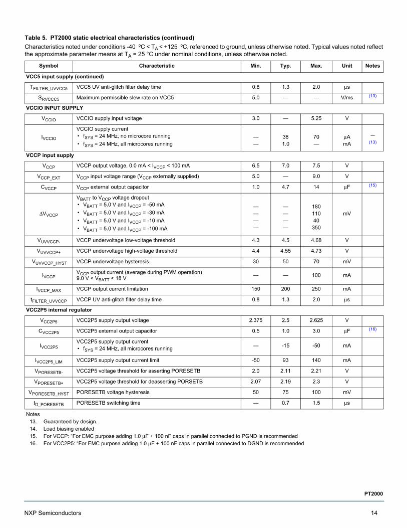
VCC5 input supply (continued)
TFILTER_UVVCC5 VCC5 UV anti-glitch filter delay time 0.8 1.3 2.0 μs
SRVCCC5 Maximum permissible slew rate on VCC5 5.0 — — V/ms (13)
VCCIO INPUT SUPPLY
VCCIO VCCIO supply input voltage 3.0 — 5.25 V
IVCCIO
VCCIO supply current• fSYS = 24 MHz, no microcore running
• fSYS = 24 MHz, all microcores running——
381.0
70—
μAmA
—
(13)
VCCP input supply
VCCP VCCP output voltage, 0.0 mA < IVCCP < 100 mA 6.5 7.0 7.5 V
VCCP_EXT VCCP input voltage range (VCCP externally supplied) 5.0 — 9.0 V
CVCCP VCCP external output capacitor 1.0 4.7 14 μF (15)
ΔVVCCP
VBATT to VCCP voltage dropout• VBATT = 5.0 V and IVCCP = -50 mA
• VBATT = 5.0 V and IVCCP = -30 mA
• VBATT = 5.0 V and IVCCP = -10 mA
• VBATT = 5.0 V and IVCCP = -100 mA
————
————
18011040
350
mV
VUVVCCP- VCCP undervoltage low-voltage threshold 4.3 4.5 4.68 V
VUVVCCP+ VCCP undervoltage high-voltage threshold 4.4 4.55 4.73 V
VUVVCCP_HYST VCCP undervoltage hysteresis 30 50 70 mV
IVCCPVCCP output current (average during PWM operation) 9.0 V < VBATT < 18 V
— — 100 mA
IVCCP_MAX VCCP output current limitation 150 200 250 mA
tFILTER_UVVCCP VCCP UV anti-glitch filter delay time 0.8 1.3 2.0 μs
VCC2P5 internal regulator
VCC2P5 VCC2P5 supply output voltage 2.375 2.5 2.625 V
CVCC2P5 VCC2P5 external output capacitor 0.5 1.0 3.0 μF (16)
IVCC2P5VCC2P5 supply output current• fSYS = 24 MHz, all microcores running
— -15 -50 mA
IVCC2P5_LIM VCC2P5 supply output current limit -50 93 140 mA
VPORESETB- VCC2P5 voltage threshold for asserting PORESETB 2.0 2.11 2.21 V
VPORESETB+ VCC2P5 voltage threshold for deasserting PORSETB 2.07 2.19 2.3 V
VPORESETB_HYST PORESETB voltage hysteresis 50 75 100 mV
tD_PORESETB PORESETB switching time — 0.7 1.5 μs
Notes13. Guaranteed by design.14. Load biasing enabled15. For VCCP: “For EMC purpose adding 1.0 μF + 100 nF caps in parallel connected to PGND is recommended16. For VCC2P5: “For EMC purpose adding 1.0 μF + 100 nF caps in parallel connected to DGND is recommended
Table 5. PT2000 static electrical characteristics (continued)
Characteristics noted under conditions -40 ºC < TA < +125 ºC, referenced to ground, unless otherwise noted. Typical values noted reflect the approximate parameter means at TA = 25 °C under nominal conditions, unless otherwise noted.
Symbol Characteristic Min. Typ. Max. Unit Notes
NXP Semiconductors 14
PT2000
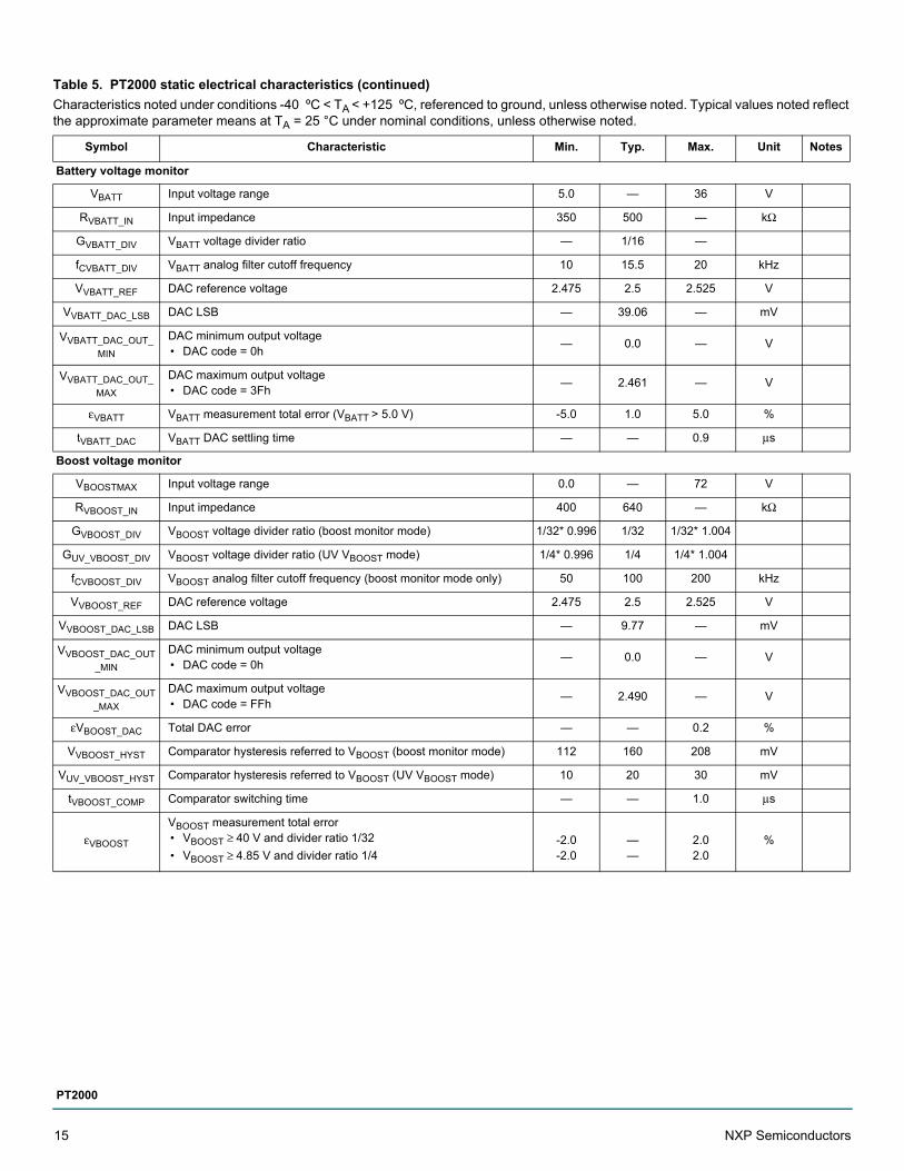
Battery voltage monitor
VBATT Input voltage range 5.0 — 36 V
RVBATT_IN Input impedance 350 500 — kΩ
GVBATT_DIV VBATT voltage divider ratio — 1/16 —
fCVBATT_DIV VBATT analog filter cutoff frequency 10 15.5 20 kHz
VVBATT_REF DAC reference voltage 2.475 2.5 2.525 V
VVBATT_DAC_LSB DAC LSB — 39.06 — mV
VVBATT_DAC_OUT_
MIN
DAC minimum output voltage• DAC code = 0h
— 0.0 — V
VVBATT_DAC_OUT_
MAX
DAC maximum output voltage• DAC code = 3Fh
— 2.461 — V
εVBATT VBATT measurement total error (VBATT > 5.0 V) -5.0 1.0 5.0 %
tVBATT_DAC VBATT DAC settling time — — 0.9 μs
Boost voltage monitor
VBOOSTMAX Input voltage range 0.0 — 72 V
RVBOOST_IN Input impedance 400 640 — kΩ
GVBOOST_DIV VBOOST voltage divider ratio (boost monitor mode) 1/32* 0.996 1/32 1/32* 1.004
GUV_VBOOST_DIV VBOOST voltage divider ratio (UV VBOOST mode) 1/4* 0.996 1/4 1/4* 1.004
fCVBOOST_DIV VBOOST analog filter cutoff frequency (boost monitor mode only) 50 100 200 kHz
VVBOOST_REF DAC reference voltage 2.475 2.5 2.525 V
VVBOOST_DAC_LSB DAC LSB — 9.77 — mV
VVBOOST_DAC_OUT
_MIN
DAC minimum output voltage• DAC code = 0h
— 0.0 — V
VVBOOST_DAC_OUT
_MAX
DAC maximum output voltage• DAC code = FFh
— 2.490 — V
εVBOOST_DAC Total DAC error — — 0.2 %
VVBOOST_HYST Comparator hysteresis referred to VBOOST (boost monitor mode) 112 160 208 mV
VUV_VBOOST_HYST Comparator hysteresis referred to VBOOST (UV VBOOST mode) 10 20 30 mV
tVBOOST_COMP Comparator switching time — — 1.0 μs
εVBOOST
VBOOST measurement total error• VBOOST ≥ 40 V and divider ratio 1/32
• VBOOST ≥ 4.85 V and divider ratio 1/4-2.0-2.0
——
2.02.0
%
Table 5. PT2000 static electrical characteristics (continued)
Characteristics noted under conditions -40 ºC < TA < +125 ºC, referenced to ground, unless otherwise noted. Typical values noted reflect the approximate parameter means at TA = 25 °C under nominal conditions, unless otherwise noted.
Symbol Characteristic Min. Typ. Max. Unit Notes
15 NXP Semiconductors
PT2000

5.3 High-side pre-driver electrical characteristics
Table 6. High-side pre-driver electrical characteristics
Characteristics noted under conditions -40 ºC < TA < +125 ºC, referenced to ground, unless otherwise noted. Typical values noted reflect the approximate parameter means at TA = 25 °C under nominal conditions, unless otherwise noted.
Symbol Characteristic Min. Typ. Max. Unit Notes
High-side pre-driver
VS_HSX
S_HSx pin operating voltageTransients t <400 nsTransients t <800 ns
-3.0-6.0-8.0
———
VBOOSTMAX——
V (17)
VB_HSX B_HSx pin operating voltageVS_HSX +
4.0—
VS_HSX + 8.0
V (17)
VBS_HSX_CL B_HSx-S_HSx clamp voltage 6.5 7.3 8.0 V (18)
VG_HSX G_HSx operating voltage VS_HSX — VB_HSX V (17)
IS_HSX_SINK_OFF
S_HSx leakage current biasing switched Off:• VS_HSX = VBOOSTMAX
• VS_HSX = 13.5 V
• VS_HSX = 7.0 V
• VS_HSX = 4.0 V
————
————
1000250120100
μA
IS_HSX_SINK_ONS_HSx leakage current when pre-driver on (biasing switched Off)• VS_HSX = 7.0 V
— — 220 μA
fG_HSX_PWM
PWM frequency• Internal VCCP and VBATT ≥ 9.0 V
• Internal VCCP and 5.0 V ≤ VBATT≤ 9.0 V
• External VCCP and 9.0 V ≤ VBATT
0.00.00.0
———
10050
100
kHz (17)
DCG_HSX Duty cycle 0.0 — 100 %
tON_HSX_MIN High-side driver minimum PWM on time — — 1.0 μs (17)
QG_HSX
External high-side MOSFET effective gate charge• fPWM ≤ fG_LSx_PWM
• fPWM ≤ 67 kHz——
4055
5075
nC
IG_HSX_PWMG_HSx current (average during PWM operation) QG = QG_HSX, fPWM = 100 kHz
— 4.0 5.0 mA (17)
IG_HSx_SRC Peak source gate drive current — 230 — mA (17)
IG_HSx_SINK Peak sink gate drive current — 440 — mA (17)
High-side pre-driver dynamic
tR_G_HSX Turn on rise time, 10%-90% of out voltage, VCCP = 7.0 V, at open pin 4.5 — 25 ns (17)
tF_G_HSX Turn off fall time, 90%-10% of out voltage, VCCP = 7.0 V, at open pin 5.0 — 25 ns (17)
SRS_HSX Max permissible slew rate at the S_HSX pin -125 — 600 V/μs (17)
tDON_G_HSX_300 Turn on propagation delay at 300 V/μs slew rate 40 — 100 ns (17)(19)
tDOFF_G_HSX_300 Turn off propagation delay at 300 V/μs slew rate 40 — 100 ns (17)(19)
tDON_G_HSX_50 Turn on propagation delay at 50 V/μs slew rate 65 — 125 ns (17)(19)
tDOFF_G_HSX_50 Turn off propagation delay at 50 V/μs slew rate 50 — 100 ns (17)(19)
Notes17. Guaranteed by design.18. VB_HSx has to be 2.0 V above PGND for full function (switch on) of the pre-driver19. 10% of output voltage change, CLOAD = 4.7 nF; RG = 40.2 Ω, VCCP = 7.0 V
NXP Semiconductors 16
PT2000
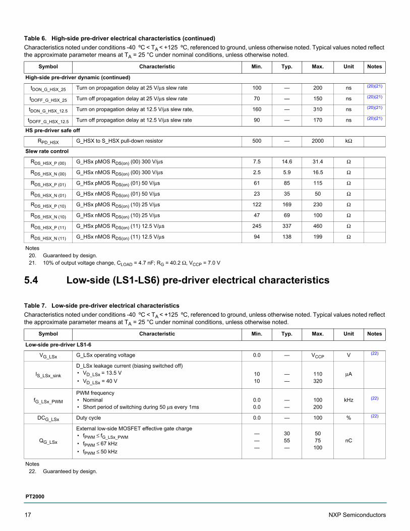
5.4 Low-side (LS1-LS6) pre-driver electrical characteristics
High-side pre-driver dynamic (continued)
tDON_G_HSX_25 Turn on propagation delay at 25 V/μs slew rate 100 — 200 ns (20)(21)
tDOFF_G_HSX_25 Turn off propagation delay at 25 V/μs slew rate 70 — 150 ns (20)(21)
tDON_G_HSX_12.5 Turn on propagation delay at 12.5 V/μs slew rate, 160 — 310 ns (20)(21)
tDOFF_G_HSX_12.5 Turn off propagation delay at 12.5 V/μs slew rate 90 — 170 ns (20)(21)
HS pre-driver safe off
RPD_HSX G_HSX to S_HSX pull-down resistor 500 — 2000 kΩ
Slew rate control
RDS_HSX_P (00) G_HSx pMOS RDS(on) (00) 300 V/μs 7.5 14.6 31.4 Ω
RDS_HSX_N (00) G_HSx nMOS RDS(on) (00) 300 V/μs 2.5 5.9 16.5 Ω
RDS_HSX_P (01) G_HSx pMOS RDS(on) (01) 50 V/μs 61 85 115 Ω
RDS_HSX_N (01) G_HSx nMOS RDS(on) (01) 50 V/μs 23 35 50 Ω
RDS_HSX_P (10) G_HSx pMOS RDS(on) (10) 25 V/μs 122 169 230 Ω
RDS_HSX_N (10) G_HSx nMOS RDS(on) (10) 25 V/μs 47 69 100 Ω
RDS_HSX_P (11) G_HSx pMOS RDS(on) (11) 12.5 V/μs 245 337 460 Ω
RDS_HSX_N (11) G_HSx nMOS RDS(on) (11) 12.5 V/μs 94 138 199 Ω
Notes20. Guaranteed by design.21. 10% of output voltage change, CLOAD = 4.7 nF; RG = 40.2 Ω, VCCP = 7.0 V
Table 7. Low-side pre-driver electrical characteristics
Characteristics noted under conditions -40 ºC < TA < +125 ºC, referenced to ground, unless otherwise noted. Typical values noted reflect the approximate parameter means at TA = 25 °C under nominal conditions, unless otherwise noted.
Symbol Characteristic Min. Typ. Max. Unit Notes
Low-side pre-driver LS1-6
VG_LSx G_LSx operating voltage 0.0 — VCCP V (22)
IS_LSx_sink
D_LSx leakage current (biasing switched off)• VD_LSx = 13.5 V
• VD_LSx = 40 V1010
——
110320
μA
fG_LSx_PWM
PWM frequency• Nominal• Short period of switching during 50 μs every 1ms
0.00.0
——
100200
kHz (22)
DCG_LSx Duty cycle 0.0 — 100 % (22)
QG_LSx
External low-side MOSFET effective gate charge• fPWM ≤ fG_LSx_PWM
• fPWM ≤ 67 kHz
• fPWM ≤ 50 kHz
———
3055—
5075
100nC
Notes22. Guaranteed by design.
Table 6. High-side pre-driver electrical characteristics (continued)
Characteristics noted under conditions -40 ºC < TA < +125 ºC, referenced to ground, unless otherwise noted. Typical values noted reflect the approximate parameter means at TA = 25 °C under nominal conditions, unless otherwise noted.
Symbol Characteristic Min. Typ. Max. Unit Notes
17 NXP Semiconductors
PT2000
Low-side pre-driver LS1-6 (continued)
IG_LSx_PWMG_LSx current (average during PWM operation)• QG = QG_LSX; fPWM = 100 kHz
— 3.0 5.0 mA (23)
IG_LSx_SRC Peak source gate drive current — 230 — mA (23), (24)
IG_LSx_SINK Peak sink gate drive current — 440 — mA (23), (24)
Dynamic low-side pre-driver LS1-6
TR_G_LSXTurn on rise time, 10% to 90% of output voltage; VCCP = 7.0 V; at open pin
5.0 — 25 ns (23)
TF_G_LSXTurn off fall time, 90% to 10% of output voltage; VCCP = 7.0 V; at open pin
5.0 — 25 ns (23)
TDON_G_LSX_300 Turn on propagation delay at 300 V/μs slew rate 10 — 70 ns (23), (25)
TDOFF_G_LSX_300 Turn off propagation delay at 300 V/μs slew rate 10 — 70 ns (23), (25)
TDON_G_LSX_50 Turn on propagation delay at 50 V/μs slew rate 10 — 80 ns (23), (25)
TDOFF_G_LSX_50 Turn off propagation delay at 50 V/μs slew rate 10 — 80 ns (23), (25)
TDON_G_LSX_25 Turn on propagation delay at 25 V/μs slew rate 15 — 120 ns (23), (25)
TDOFF_G_LSX_25 Turn off propagation delay at 25 V/μs slew rate 15 — 120 ns (23), (25)
TDON_G_LSX_12.5 Turn on propagation delay at 12.5 V/μs slew rate 15 — 150 ns (23), (25)
TDOFF_G_LSX_12.5 Turn off propagation delay at 12.5 V/μs slew rate 15 — 150 ns (23), (25)
LS pre-driver safe off
RPD_LSX G_LSX to PGND pull-down resistor 25 50 90 kΩ
Low-side pre-driver LS1-6
RDS_LSX_P (00) G_LSx pMOS RDS(on) (00) 300 V/μs 7.5 14.6 31.3 Ω
RDS_LSX_N (00) G_LSx nMOS RDS(on) (00) 300 V/μs 2.5 5.9 16.5 Ω
RDS_LSX_P (01) G_LSx pMOS RDS(on)n (01) 50 V/μs 61 84 115 Ω
RDS_LSX_N (01) G_LSx nMOS RDS(on) (01) 50 V/μs 23 35 50 Ω
RDS_LSX_P (10) G_LSx pMOS RDS(on) (10) 25 V/μs 122 170 230 Ω
RDS_LSX_N (10) G_LSx nMOS RDS(on) (10) 25 V/μs 47 69 100 Ω
RDS_LSX_P (11) G_LSx pMOS RDS(on) (11) 12.5 V/μs 245 337 460 Ω
RDS_LSX_N (11) G_LSx nMOS RDS(on) (11) 12.5 V/μs 94 138 199 Ω
Notes23. Guaranteed by design.24. VCCP = VGS = 7.0 V and fastest slew rate
25. 10% of output voltage change; CLOAD = 4.7 nF; RG = 40.2 Ω; VCCP = 7.0 V
Table 7. Low-side pre-driver electrical characteristics (continued)
Characteristics noted under conditions -40 ºC < TA < +125 ºC, referenced to ground, unless otherwise noted. Typical values noted reflect the approximate parameter means at TA = 25 °C under nominal conditions, unless otherwise noted.
Symbol Characteristic Min. Typ. Max. Unit Notes
NXP Semiconductors 18
PT2000
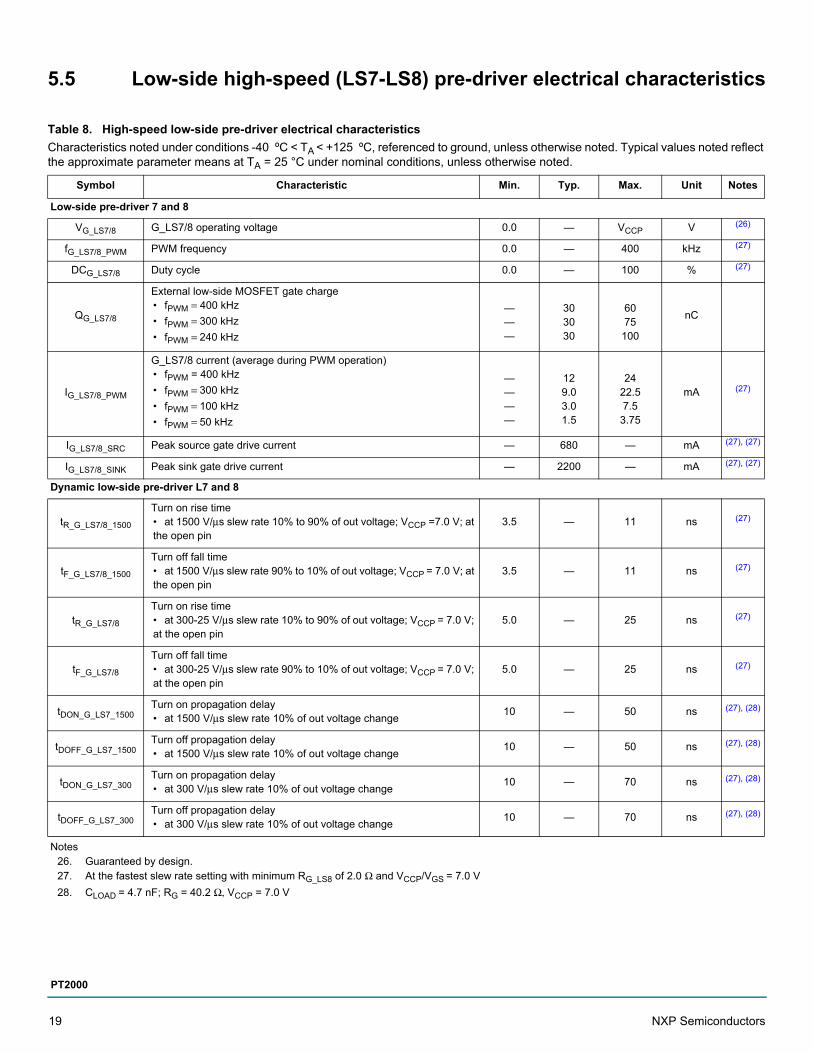
5.5 Low-side high-speed (LS7-LS8) pre-driver electrical characteristics
Table 8. High-speed low-side pre-driver electrical characteristics
Characteristics noted under conditions -40 ºC < TA < +125 ºC, referenced to ground, unless otherwise noted. Typical values noted reflect the approximate parameter means at TA = 25 °C under nominal conditions, unless otherwise noted.
Symbol Characteristic Min. Typ. Max. Unit Notes
Low-side pre-driver 7 and 8
VG_LS7/8 G_LS7/8 operating voltage 0.0 — VCCP V (26)
fG_LS7/8_PWM PWM frequency 0.0 — 400 kHz (27)
DCG_LS7/8 Duty cycle 0.0 — 100 % (27)
QG_LS7/8
External low-side MOSFET gate charge• fPWM = 400 kHz
• fPWM = 300 kHz
• fPWM = 240 kHz
———
303030
6075
100
nC
IG_LS7/8_PWM
G_LS7/8 current (average during PWM operation)• fPWM = 400 kHz
• fPWM = 300 kHz
• fPWM = 100 kHz
• fPWM = 50 kHz
————
129.03.01.5
2422.57.5
3.75
mA (27)
IG_LS7/8_SRC Peak source gate drive current — 680 — mA (27), (27)
IG_LS7/8_SINK Peak sink gate drive current — 2200 — mA (27), (27)
Dynamic low-side pre-driver L7 and 8
tR_G_LS7/8_1500
Turn on rise time• at 1500 V/μs slew rate 10% to 90% of out voltage; VCCP =7.0 V; at the open pin
3.5 — 11 ns (27)
tF_G_LS7/8_1500
Turn off fall time• at 1500 V/μs slew rate 90% to 10% of out voltage; VCCP = 7.0 V; at the open pin
3.5 — 11 ns (27)
tR_G_LS7/8
Turn on rise time• at 300-25 V/μs slew rate 10% to 90% of out voltage; VCCP = 7.0 V; at the open pin
5.0 — 25 ns (27)
tF_G_LS7/8
Turn off fall time• at 300-25 V/μs slew rate 90% to 10% of out voltage; VCCP = 7.0 V; at the open pin
5.0 — 25 ns (27)
tDON_G_LS7_1500Turn on propagation delay• at 1500 V/μs slew rate 10% of out voltage change
10 — 50 ns (27), (28)
tDOFF_G_LS7_1500Turn off propagation delay• at 1500 V/μs slew rate 10% of out voltage change
10 — 50 ns (27), (28)
tDON_G_LS7_300Turn on propagation delay• at 300 V/μs slew rate 10% of out voltage change
10 — 70 ns (27), (28)
tDOFF_G_LS7_300Turn off propagation delay• at 300 V/μs slew rate 10% of out voltage change
10 — 70 ns (27), (28)
Notes26. Guaranteed by design.27. At the fastest slew rate setting with minimum RG_LS8 of 2.0 Ω and VCCP/VGS = 7.0 V
28. CLOAD = 4.7 nF; RG = 40.2 Ω, VCCP = 7.0 V
19 NXP Semiconductors
PT2000
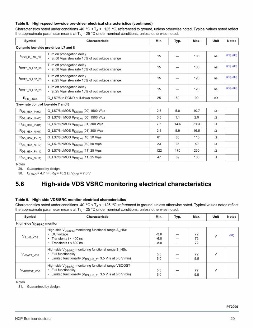
5.6 High-side VDS VSRC monitoring electrical characteristics
Dynamic low-side pre-driver L7 and 8
tDON_G_LS7_50Turn on propagation delay• at 50 V/μs slew rate 10% of out voltage change
15 — 100 ns (29), (30)
tDOFF_G_LS7_50Turn off propagation delay• at 50 V/μs slew rate 10% of out voltage change
15 — 100 ns (29), (30)
tDOFF_G_LS7_25Turn off propagation delay• at 25 V/μs slew rate 10% of out voltage change
15 — 120 ns (29), (30)
tDOFF_G_LS7_25Turn off propagation delay• at 25 V/μs slew rate 10% of out voltage change
15 — 120 ns (29), (30)
RPD_LS7/8 G_LS7/8 to PGND pull-down resistor 25 50 90 kΩ
Slew rate control low-side 7 and 8
RDS_HSX_P (00) G_LS7/8 pMOS RDS(on) (00) 1500 V/μs 2.6 5.0 10.7 Ω
RDS_HSX_N (00) G_LS7/8 nMOS RDS(on) (00) 1500 V/μs 0.5 1.1 2.9 Ω
RDS_HSX_P (01) G_LS7/8 pMOS RDS(on) (01) 300 V/μs 7.5 14.6 31.3 Ω
RDS_HSX_N (01) G_LS7/8 nMOS RDS(on) (01) 300 V/μs 2.5 5.9 16.5 Ω
RDS_HSX_P (10) G_LS7/8 pMOS RDS(on) (10) 50 V/μs 61 85 115 Ω
RDS_HSX_N (10) G_LS7/8 nMOS RDS(on) (10) 50 V/μs 23 35 50 Ω
RDS_HSX_P (11) G_LS7/8 pMOS RDS(on) (11) 25 V/μs 122 170 230 Ω
RDS_HSX_N (11) G_LS7/8 nMOS RDS(on) (11) 25 V/μs 47 69 100 Ω
Notes29. Guaranteed by design.30. CLOAD = 4.7 nF; RG = 40.2 Ω, VCCP = 7.0 V
Table 9. High-side VDS/SRC monitor electrical characteristics Characteristics noted under conditions -40 ºC < TA < +125 ºC, referenced to ground, unless otherwise noted. Typical values noted reflect the approximate parameter means at TA = 25 °C under nominal conditions, unless otherwise noted.
Symbol Characteristic Min. Typ. Max. Unit Notes
High-side VDS/SRC monitor
VS_HS_VDS
High-side VDS/SRC monitoring functional range S_HSx• DC voltage• Transients t < 400 ns• Transients t < 800 ns
-3.0-6.0-8.0
———
727272
V (31)
VVBATT_VDS
High-side VDS/SRC monitoring functional range S_HSx• Full functionality• Limited functionality (VDS_HS_Th 3.5 V is at 3.0 V min)
5.55.0
——
725.5
V
VVBOOST_VDS
High-side VDS/SRC monitoring functional range VBOOST• Full functionality• Limited functionality (VDS_HS_Th 3.5 V is at 3.0 V min)
5.55.0
——
725.5
V
Notes31. Guaranteed by design.
Table 8. High-speed low-side pre-driver electrical characteristics (continued)
Characteristics noted under conditions -40 ºC < TA < +125 ºC, referenced to ground, unless otherwise noted. Typical values noted reflect the approximate parameter means at TA = 25 °C under nominal conditions, unless otherwise noted.
Symbol Characteristic Min. Typ. Max. Unit Notes
NXP Semiconductors 20
PT2000
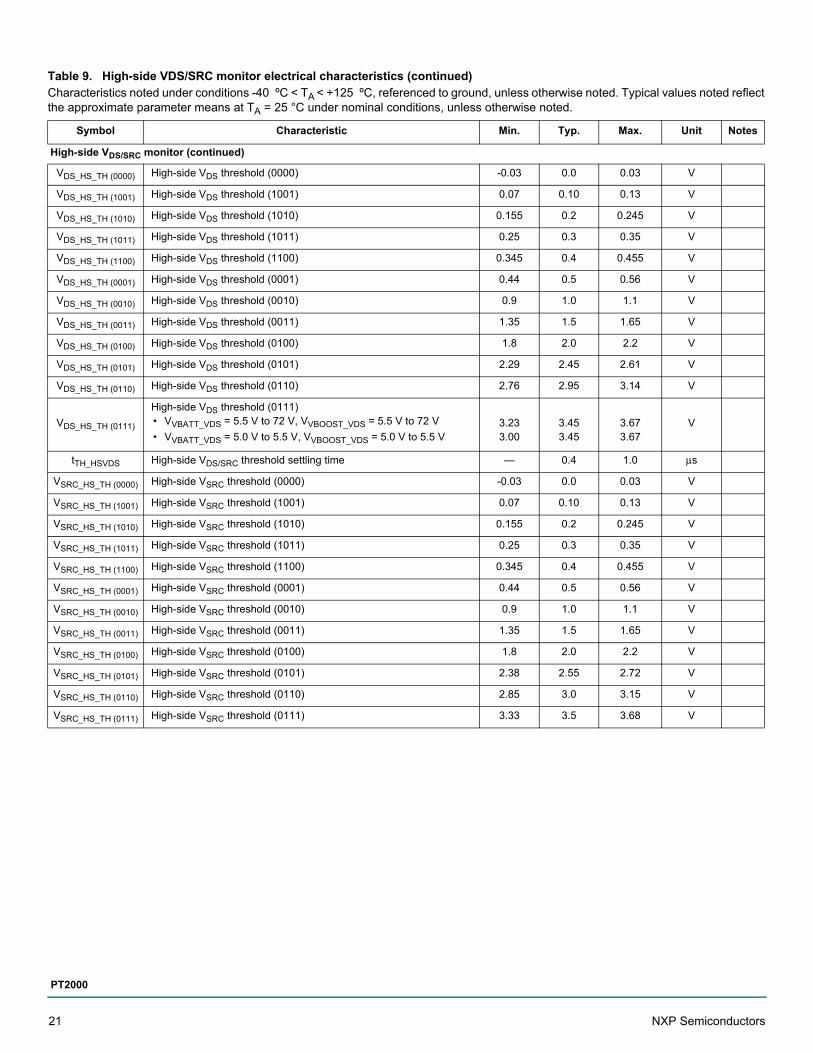
High-side VDS/SRC monitor (continued)
VDS_HS_TH (0000) High-side VDS threshold (0000) -0.03 0.0 0.03 V
VDS_HS_TH (1001) High-side VDS threshold (1001) 0.07 0.10 0.13 V
VDS_HS_TH (1010) High-side VDS threshold (1010) 0.155 0.2 0.245 V
VDS_HS_TH (1011) High-side VDS threshold (1011) 0.25 0.3 0.35 V
VDS_HS_TH (1100) High-side VDS threshold (1100) 0.345 0.4 0.455 V
VDS_HS_TH (0001) High-side VDS threshold (0001) 0.44 0.5 0.56 V
VDS_HS_TH (0010) High-side VDS threshold (0010) 0.9 1.0 1.1 V
VDS_HS_TH (0011) High-side VDS threshold (0011) 1.35 1.5 1.65 V
VDS_HS_TH (0100) High-side VDS threshold (0100) 1.8 2.0 2.2 V
VDS_HS_TH (0101) High-side VDS threshold (0101) 2.29 2.45 2.61 V
VDS_HS_TH (0110) High-side VDS threshold (0110) 2.76 2.95 3.14 V
VDS_HS_TH (0111)
High-side VDS threshold (0111)• VVBATT_VDS = 5.5 V to 72 V, VVBOOST_VDS = 5.5 V to 72 V
• VVBATT_VDS = 5.0 V to 5.5 V, VVBOOST_VDS = 5.0 V to 5.5 V3.233.00
3.453.45
3.673.67
V
tTH_HSVDS High-side VDS/SRC threshold settling time — 0.4 1.0 μs
VSRC_HS_TH (0000) High-side VSRC threshold (0000) -0.03 0.0 0.03 V
VSRC_HS_TH (1001) High-side VSRC threshold (1001) 0.07 0.10 0.13 V
VSRC_HS_TH (1010) High-side VSRC threshold (1010) 0.155 0.2 0.245 V
VSRC_HS_TH (1011) High-side VSRC threshold (1011) 0.25 0.3 0.35 V
VSRC_HS_TH (1100) High-side VSRC threshold (1100) 0.345 0.4 0.455 V
VSRC_HS_TH (0001) High-side VSRC threshold (0001) 0.44 0.5 0.56 V
VSRC_HS_TH (0010) High-side VSRC threshold (0010) 0.9 1.0 1.1 V
VSRC_HS_TH (0011) High-side VSRC threshold (0011) 1.35 1.5 1.65 V
VSRC_HS_TH (0100) High-side VSRC threshold (0100) 1.8 2.0 2.2 V
VSRC_HS_TH (0101) High-side VSRC threshold (0101) 2.38 2.55 2.72 V
VSRC_HS_TH (0110) High-side VSRC threshold (0110) 2.85 3.0 3.15 V
VSRC_HS_TH (0111) High-side VSRC threshold (0111) 3.33 3.5 3.68 V
Table 9. High-side VDS/SRC monitor electrical characteristics (continued)Characteristics noted under conditions -40 ºC < TA < +125 ºC, referenced to ground, unless otherwise noted. Typical values noted reflect the approximate parameter means at TA = 25 °C under nominal conditions, unless otherwise noted.
Symbol Characteristic Min. Typ. Max. Unit Notes
21 NXP Semiconductors
PT2000
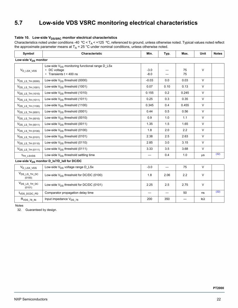
5.7 Low-side VDS VSRC monitoring electrical characteristics
Table 10. Low-side VDS/SRC monitor electrical characteristics Characteristics noted under conditions -40 ºC < TA < +125 ºC, referenced to ground, unless otherwise noted. Typical values noted reflect the approximate parameter means at TA = 25 °C under nominal conditions, unless otherwise noted.
Symbol Characteristic Min. Typ. Max. Unit Notes
Low-side VDS monitor
VD_LSX_VDS
Low-side VDS monitoring functional range D_LSx• DC voltage• Transients t < 400 ns
-3.0-8.0
——
7575
V
VDS_LS_TH (0000) Low-side VDS threshold (0000) -0.03 0.0 0.03 V
VDS_LS_TH (1001) Low-side VDS threshold (1001) 0.07 0.10 0.13 V
VDS_LS_TH (1010) Low-side VDS threshold (1010) 0.155 0.2 0.245 V
VDS_LS_TH (1011) Low-side VDS threshold (1011) 0.25 0.3 0.35 V
VDS_LS_TH (1100) Low-side VDS threshold (1100) 0.345 0.4 0.455 V
VDS_LS_TH (0001) Low-side VDS threshold (0001) 0.44 0.5 0.56 V
VDS_LS_TH (0010) Low-side VDS threshold (0010) 0.9 1.0 1.1 V
VDS_LS_TH (0011) Low-side VDS threshold (0011) 1.35 1.5 1.65 V
VDS_LS_TH (0100) Low-side VDS threshold (0100) 1.8 2.0 2.2 V
VDS_LS_TH (0101) Low-side VDS threshold (0101) 2.38 2.5 2.63 V
VDS_LS_TH (0110) Low-side VDS threshold (0110) 2.85 3.0 3.15 V
VDS_LS_TH (0111) Low-side VDS threshold (0111) 3.33 3.5 3.68 V
tTH_LSVDS Low-side VDS threshold settling time — 0.4 1.0 μs (32)
Low-side VDS monitor D_ls7/D_ls8 for DC/DC
VD_LSX_VDS Low-side VDS voltage range D_LSx -3.0 — 75 V
VDS_LS_TH_DC
(0100)Low-side VDS threshold for DC/DC (0100) 1.8 2.06 2.2 V
VDS_LS_TH_DC
(0101)Low-side VDS threshold for DC/DC (0101) 2.25 2.5 2.75 V
tVDS_DCDC_PD Comparator propagation delay time — — 50 ns (32)
RVDS_78_IN Input impedance VDS_78 200 350 — kΩ
Notes32. Guaranteed by design.
NXP Semiconductors 22
PT2000
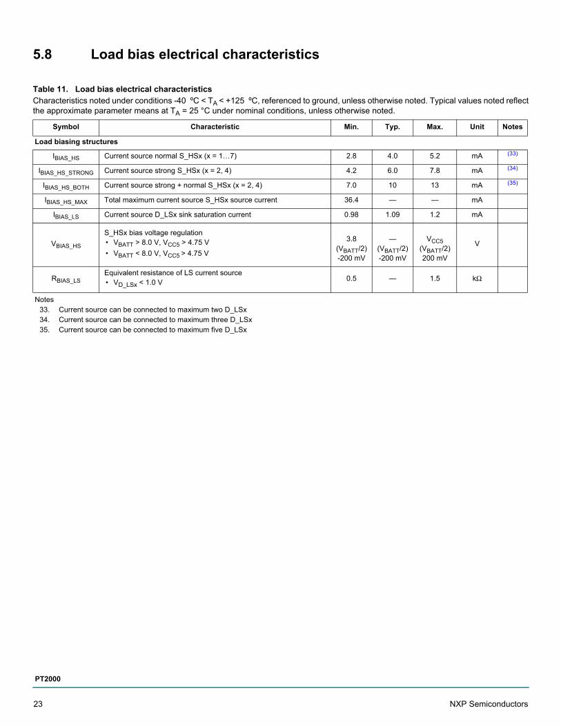
5.8 Load bias electrical characteristics
Table 11. Load bias electrical characteristics Characteristics noted under conditions -40 ºC < TA < +125 ºC, referenced to ground, unless otherwise noted. Typical values noted reflect the approximate parameter means at TA = 25 °C under nominal conditions, unless otherwise noted.
Symbol Characteristic Min. Typ. Max. Unit Notes
Load biasing structures
IBIAS_HS Current source normal S_HSx (x = 1…7) 2.8 4.0 5.2 mA (33)
IBIAS_HS_STRONG Current source strong S_HSx (x = 2, 4) 4.2 6.0 7.8 mA (34)
IBIAS_HS_BOTH Current source strong + normal S_HSx (x = 2, 4) 7.0 10 13 mA (35)
IBIAS_HS_MAX Total maximum current source S_HSx source current 36.4 — — mA
IBIAS_LS Current source D_LSx sink saturation current 0.98 1.09 1.2 mA
VBIAS_HS
S_HSx bias voltage regulation• VBATT > 8.0 V, VCC5 > 4.75 V
• VBATT < 8.0 V, VCC5 > 4.75 V
3.8(VBATT/2)-200 mV
—(VBATT/2)-200 mV
VCC5(VBATT/2)200 mV
V
RBIAS_LSEquivalent resistance of LS current source• VD_LSx < 1.0 V 0.5 — 1.5 kΩ
Notes33. Current source can be connected to maximum two D_LSx34. Current source can be connected to maximum three D_LSx35. Current source can be connected to maximum five D_LSx
23 NXP Semiconductors
PT2000

5.9 Current measurement electrical characteristics
5.9.1 Current measurement for positive currentThis section is applicable for all current measurement paths for positive currents:
• Current measurement channel 1- 4• Differential amplifier 1- 4• DAC 1- 4• Comparator 1- 4
• Current measurement channel 5 - 6• Differential amplifier 5 - 6• DAC 5 - 6H and DAC 5 - 6L• Comparator 5 - 6H and 5 - 6L
Table 12. Current measurement for positive currents
Symbol CharacteristicStatistically evaluated
Unit Notes
εCS
Overall current sense error including gain errors and offsets at DAC range of 75% -100%, after analog offset compensation• at GDA_diff (00) = 5.8• at GDA_diff (01) = 8.7• at GDA_diff (10) = 12.6• at GDA_diff (11) = 19.3
±3.5±3.5±3.5±3.5
% (36), (37)
At DAC range of 25% to 75%, after analog offset compensation• at GDA_diff (00) = 5.8• at GDA_diff (01) = 8.7• at GDA_diff (10) = 12.6• at GDA_diff (11) = 19.3
±5.3±5.3±5.3±5.3
% (36), (37)
Notes36. Guaranteed by design.37. The tolerance of the 10 mΩ shunt resistor is assumed as ±2.0% (at 4.5 σ). All other input tolerances from the device specification are assumed
at 6 σ.
Table 13. Differential amplifier 1, 2, 3, 4, 5, and 6
Characteristics noted under conditions -40 ºC < TA < +125 ºC, referenced to ground, unless otherwise noted. Typical values noted reflect the approximate parameter means at TA = 25 °C under nominal conditions, unless otherwise noted.
Symbol Characteristic Min. Typ. Max. Unit Notes
VVSENSENX_DA Differential amplifier x functional range VSENSENx (x = 1…6) -1.0 — 1.0 V
VVSENSEPX_DA Differential amplifier x functional range VSENSEPx (x = 1…6) -1.0 — 1.5 V
VDA_DIFF_IN (00)Differential input voltage range (00) • GDA_DIFF(00) = 5.8 -25.9 — 387 mV
VDA_DIFF_IN (01)Differential input voltage range (01)• GDA_DIFF(01) = 8.7 -17.3 — 258 mV
VDA_DIFF_IN (10)Differential input voltage range (10)• GDA_DIFF(10) = 12.6 -12 — 179 mV
VDA_DIFF_IN (11)Differential input voltage range (11)• GDA_DIFF(11) = 19.3 -7.8 — 116 mV
GDA_DIFF (00) Differential voltage gain (00) 5.71 5.79 5.87
GDA_DIFF (01) Differential voltage gain (01) 8.55 8.68 8.81
GDA_DIFF (10) Differential voltage gain (10) 12.32 12.53 12.74
NXP Semiconductors 24
PT2000
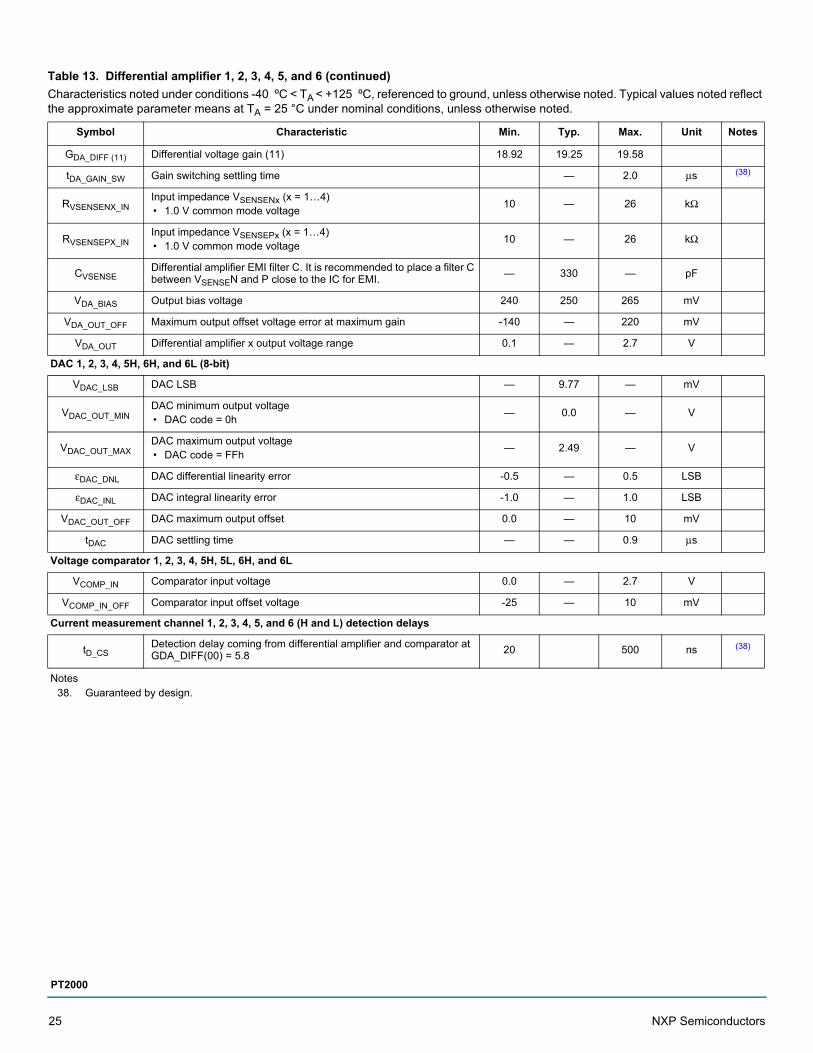
GDA_DIFF (11) Differential voltage gain (11) 18.92 19.25 19.58
tDA_GAIN_SW Gain switching settling time — 2.0 μs (38)
RVSENSENX_INInput impedance VSENSENx (x = 1…4)• 1.0 V common mode voltage
10 — 26 kΩ
RVSENSEPX_INInput impedance VSENSEPx (x = 1…4)• 1.0 V common mode voltage
10 — 26 kΩ
CVSENSEDifferential amplifier EMI filter C. It is recommended to place a filter C between VSENSEN and P close to the IC for EMI.
— 330 — pF
VDA_BIAS Output bias voltage 240 250 265 mV
VDA_OUT_OFF Maximum output offset voltage error at maximum gain -140 — 220 mV
VDA_OUT Differential amplifier x output voltage range 0.1 — 2.7 V
DAC 1, 2, 3, 4, 5H, 6H, and 6L (8-bit)
VDAC_LSB DAC LSB — 9.77 — mV
VDAC_OUT_MINDAC minimum output voltage• DAC code = 0h
— 0.0 — V
VDAC_OUT_MAXDAC maximum output voltage• DAC code = FFh
— 2.49 — V
εDAC_DNL DAC differential linearity error -0.5 — 0.5 LSB
εDAC_INL DAC integral linearity error -1.0 — 1.0 LSB
VDAC_OUT_OFF DAC maximum output offset 0.0 — 10 mV
tDAC DAC settling time — — 0.9 μs
Voltage comparator 1, 2, 3, 4, 5H, 5L, 6H, and 6L
VCOMP_IN Comparator input voltage 0.0 — 2.7 V
VCOMP_IN_OFF Comparator input offset voltage -25 — 10 mV
Current measurement channel 1, 2, 3, 4, 5, and 6 (H and L) detection delays
tD_CSDetection delay coming from differential amplifier and comparator at GDA_DIFF(00) = 5.8
20 500 ns (38)
Notes38. Guaranteed by design.
Table 13. Differential amplifier 1, 2, 3, 4, 5, and 6 (continued)
Characteristics noted under conditions -40 ºC < TA < +125 ºC, referenced to ground, unless otherwise noted. Typical values noted reflect the approximate parameter means at TA = 25 °C under nominal conditions, unless otherwise noted.
Symbol Characteristic Min. Typ. Max. Unit Notes
25 NXP Semiconductors
PT2000
5.9.2 Current measurement for negative currentsThis section is applicable for all current measurement paths for negative currents:
• Current measurement channel 5 and 6• Differential amplifier 5 and 6 negative• DAC 5 and 6 negative• Comparator 5 and 6 negative
Differential amplifier 1, 2, 3, 4, 5, and 6 analog offset compensation
VOFFDAC_OUT_MAX
_POSVOFFDAC_OUT_MAX
_NEG
Offset compensation voltage range referred to amplifier output offset at maximum gain• Offset DAC value = +31• Offset DAC value = -31
150-310
——
310-150
mV (40)
VOFFDAC_LSBOffset compensation step size referred to amplifier output offset at maximum gain
5.0 — 10 mV
VCS_OFF_TEMP Differential amplifier output offset temperature drift-5.0-50
——
5.050
LSBmV
(39)
VCS_OFF_GDResidual offset after offset compensation at diff amplifier output for path shunt ≥ comparator output
-0.61-6.1
——
0.393.9
LSBmV
(41)
tOFFCOMP_STEP Offset compensation minimum step time — — 2.0 μs (40)
tOFFCOMP Offset compensation runtime to finish compensation — — 2.0*31 = 62 μs (40)(42)
Notes39. Guaranteed by design.40. Gain set to GDA_DIFF(11) = 19.3
41. The offset compensation algorithm is implemented so the compensation always stops when the comparator output signal is low, assuming a zero DAC gain error and INL.
42. Assuming the start from an offset compensation DAC value of 0 is worst case, it has to go to one extreme value (-31 or 31).
Table 14. PT2000 static electrical characteristics
Characteristics noted under conditions -40 ºC < TA < +125 ºC, referenced to ground, unless otherwise noted. Typical values noted reflect the approximate parameter means at TA = 25 °C under nominal conditions, unless otherwise noted.
Symbol Characteristic Min. Typ. Max. Unit Notes
Overall current sense performance for negative
εCSNEG
Overall current sense error including gain errors and offsets• at DAC range of 75% to 100% at GDANEG_DIFF = -2.0
• at DAC range of 25% to 75% at GDANEG_DIFF = -2.0——
——
±4.4±8.9
% (43), (44)
Differential amplifier 5, 6 negative
VVSENSEN5/6_DANEG
Differential amplifier 5 and 6 negative (negative currents) functional range VSENSE N5/6
-3.0 — 1.0 V (43)
VVSENSEP5/6_DANEG
Differential amplifier 5 and 6 negative (negative currents) functional range VSENSE P5/6
-4.2 — 1.0 V (43)
VDANEG_DIFF_INDifferential input voltage range• GDANEG_DIFF = -2.0 -1.125 — 0.0 V (43)
GDANEG_DIFF Differential voltage gain -1.966 -2.0 -2.034
RVSENSEN5/6_INInput impedance VSENSE N5/6• 1.0 V common mode voltage
6.0 — 14 kΩ
Table 13. Differential amplifier 1, 2, 3, 4, 5, and 6 (continued)
Characteristics noted under conditions -40 ºC < TA < +125 ºC, referenced to ground, unless otherwise noted. Typical values noted reflect the approximate parameter means at TA = 25 °C under nominal conditions, unless otherwise noted.
Symbol Characteristic Min. Typ. Max. Unit Notes
NXP Semiconductors 26
PT2000
Differential amplifier 5, 6 negative (continued)
RVSENSEP5/6_INInput impedance VSENSE P5/6• 1.0 V common mode voltage
6.0 — 14 kΩ
VDANEG_IN_OFF Differential amplifier maximum input offset voltage -20 — 20 mV
VDANEG_BIAS Output bias voltage 240 250 265 mV
VDANEG_OUT_OFFMaximum output offset voltage error, including amplifier input offset and bias voltage offset.
-60 — 60 mV
VDANEG_OUT Differential amplifier x output voltage range 0.0 — 2.7 V
DAC 5 Neg and 6 Neg (4 Bit)
VDACNEG_LSB DAC LSB — 156.3 — mV
VDACNEG_OUT_MINDAC minimum output voltage• DAC code = 0h
— 0.0 — V
VDACNEG_OUT_MAXDAC maximum output voltage• DAC code = Fh
— 2.344 — V
εDACNEG_GAINDAC maximum gain error• Error of bandgap reference voltage
-1.0 — 1.0 %
εDACNEG_DNL DAC differential linearity error -0.063 — 0.063 LSB
εDACNEG_INL DAC integral linearity error -0.063 — 0.063 LSB
VDACNEG_OUT_OFF DAC maximum output offset 0.0 — 10 mV
tDACNEG DAC settling time — — 0.9 μs
Voltage comparator 5 Neg and 6 Neg
VCOMP_IN Comparator input voltage 0.0 — 2.7 V
VCOMP_IN_OFF Comparator input offset voltage -25 — 10 mV
Current measurement channel 5 Neg and 6 Neg detection delays
tD_CSNEGDetection delay coming from differential amplifier and comparator• GDANEG_DIFF = -2.0
20 — 500 ns (45)
Notes43. Guaranteed by design.
44. The tolerance of the 10 mΩ shunt resistor is assumed as ±2.0% (at 4.5 σ). All other input tolerances from the device specification are assumed at 6 σ
45. Guaranteed by design.
Table 14. PT2000 static electrical characteristics (continued)
Characteristics noted under conditions -40 ºC < TA < +125 ºC, referenced to ground, unless otherwise noted. Typical values noted reflect the approximate parameter means at TA = 25 °C under nominal conditions, unless otherwise noted.
Symbol Characteristic Min. Typ. Max. Unit Notes
27 NXP Semiconductors
PT2000
5.10 Analog output (OAx) electrical characteristics
Table 15. Analog output static electrical characteristics Characteristics noted under conditions -40 ºC < TA < +125 ºC, referenced to ground, unless otherwise noted. Typical values noted reflect the approximate parameter means at TA = 25 °C under nominal conditions, unless otherwise noted.
Symbol Characteristic Min. Typ. Max. Unit Notes
OAx output PiNS, multiplexer and T&H
VOAX OAx output voltage range 0.0 — VCC5 V
BWOAX OAx output bandwidth 100 — — kHz (46)
COAX
OAx permissible capacitive load• without series resistor, for digital function• RMIN = 200 Ω• RMIN = 100 Ω• RMIN = 75 Ω• RMIN = 50 Ω
—1.05.01550
—————
505.01550
100
pFnFnFnFnF
(46)
PSRROAX OAx power supply rejection — — 103 dB (46)
GOAX(00) OAx output gain (00) 1.303 1.33 1.357
GOAX(01) OAx output gain (01) 1.940 2.0 2.060
GOAX(10) OAx output gain (10) 2.91 3.0 3.090
GOAX(11) OAx output gain (11) 5.17 5.33 5.49
GOAX(ADC) OAx output gain (ADC) 0.98 1.0 1.02
tOAX_GAIN OAx output gain switching time — — 2.0 μs (46)
VOAX_OFFSET
OAx output offset voltage from OAx amplifier• GOAx = 1.0
• GOAx = 1.33
• GOAx = 2.0
• GOAx = 3.0
• GOAx = 5.33
-14-18-28-30-53
—————
1418283053
mV
ROA1/3_EN0OA1/3 input impedance when OaENx = 0• 2.0 V, impedance to GND
— — 8000 kΩ
ROA2_EN0OA2 input impedance when OaENx = 0• 2.0 V, impedance to GND
350 — 500 kΩ
tOAX_MUX OAx multiplexer switching time — — 10 μs (46)
VOAX_DRIFT_ADCOAx output voltage drift of T&H in ADC mode over time• at VOAx = 1.5 V and after 20 μs
-50 — 50 mV
Notes46. Guaranteed by design.
NXP Semiconductors 28
PT2000
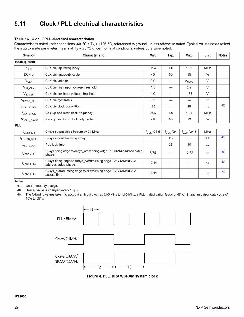
5.11 Clock / PLL electrical characteristics
Table 16. Clock / PLL electrical characteristics Characteristics noted under conditions -40 ºC < TA < +125 ºC, referenced to ground, unless otherwise noted. Typical values noted reflect the approximate parameter means at TA = 25 °C under nominal conditions, unless otherwise noted.
Symbol Characteristic Min. Typ. Max. Unit Notes
Backup clock
fCLK CLK pin input frequency 0.94 1.0 1.06 MHz
DCCLK CLK pin input duty cycle 45 50 55 %
VCLK CLK pin voltage 0.0 — VCCIO V
VIH_CLK CLK pin high input voltage threshold 1.5 — 2.2 V
VIL_CLK CLK pin low input voltage threshold 1.0 — 1.65 V
VHYST_CLK CLK pin hysteresis 0.3 — — V
tCLK_JITTER CLK pin clock edge jitter -25 — 25 ns (47)
fCLK_BACK Backup oscillator clock frequency 0.95 1.0 1.05 MHz
DCCLK_BACK Backup oscillator clock duty cycle 48 50 52 %
PLL
fCKSYS24 Cksys output clock frequency 24 MHz fCLK *23.5 fCLK *24 fCLK *24.5 MHz
fCKSYS_MOD Cksys modulation frequency — 25 — kHz (48)
tPLL _LOCK PLL lock time — 25 40 μs
tCKSYS_T1Cksys rising edge to cksys_cram rising edge T1 CRAM address setup phase
8.75 — 12.32 ns (49)
tCKSYS_T2Cksys rising edge to cksys_c/dram rising edge T2 CRAM/DRAM address setup phase
19.44 — — ns (49)
tCKSYS_T3Cksys_c/dram rising edge to cksys rising edge T3 CRAM/DRAM access time
19.44 — — ns (49)
Notes47. Guaranteed by design.48. Divider value is changed every 10 μs49. The following values take into account an input clock at 0.95 MHz to 1.05 MHz, a PLL multiplication factor of 47 to 49, and an output duty cycle of
45% to 55%.
Figure 4. PLL, DRAM/CRAM system clock
T1
T2 T3
PLL 48MHz
Cksys 24MHz
Cksys CRAM/DRAM 24MHz
29 NXP Semiconductors
PT2000

5.12 Digital input/output electrical characteristics
Table 17. PT2000 static electrical characteristics
Characteristics noted under conditions -40 ºC < TA < +125 ºC, referenced to ground, unless otherwise noted. Typical values noted reflect the approximate parameter means at TA = 25 °C under nominal conditions, unless otherwise noted.
Symbol Characteristic Min. Typ. Max. Unit Notes
Digital I/OS
VIOVCCIODigital pins voltage (IRQB, MISO, MOSI, SCLK, CSB, Startx, Flagx, DBG, OAx)
0.0 — VCCIO V
VIOVCC5 Digital pins voltage (RESETB, DRVEN) 0.0 — VCC5 V
tDIGIOREADY Digital output ready time after POResetB deactivation — — 100 μs
tFILT_RESETB RESETB filter time 0.2 — 2.0 μs
VIH_IODigital pins high input voltage threshold (RESETB, IRQB, MOSI, SCLK, CSB, DRVEN, Startx, Flagx, DBG, OAx)
1.5 — 2.2 V
VIL_IODigital pins low input voltage threshold (RESETB, IRQB, MOSI, SCLK, CSB, DRVEN, STARTx, FLAGx, DBG, OAx)
1.0 — 1.65 V
VHYST_IODigital pins hysteresis (RESETB, IRQB, MOSI, SCLK, CSB, DRVEN, STARTx, FLAGx, DBG, OAx)
0.3 — — V
VOH_IO
Digital pins high output voltage (IRQB, MISO, START1-7, FLAG0-3, DBG)• IOUT > -1.0 mA, no higher current at other I/Os
VCCIO -0.3 — — V
VOL_IO
Digital pins low output voltage (IRQB, MISO, START1-7, FLAG0-3, DBG)• IOUT < 1.0 mA, no higher current at other I/Os
— — 0.3 V
VOH_ START8/FLAG4Digital pins high output voltage (Start8, Flag4)• IOUT > -200 μA
VCC0 -0.6 — — V
VOL_ START8/FLAG4Digital pins low output voltage (Start8, Flag4)• IOUT > -200 μA
— — 0.6 V
VOH_OA2
Digital pins high output voltage (OA2)• GOAx = 1.33, IOUT > -1.0 mA
• GOAx = 2.0, IOUT > -1.0 mA2.8
VCC5 -0.6——
——
V
VOL_OA2 Digital pins low output voltage (OA2), IOUT < 0.5 mA — — 0.3 V
tR_XXXDigital pins output rise time (IRQB, START1-7, FLAG0-3, DBG)• CLOAD = 30 pF, 10%-90% of out voltage
3.0 — 12 ns
tF_XXXDigital pins output fall time (IRQB, START1-7, FLAG0-3, DBG)• CLOAD = 30 pF, 90%-10% of out voltage
3.0 — 12 ns
tD_XXXDigital pins output delay (IRQB, START1-7, FLAG0-3, DBG)• CLOAD = 30 pF, 10% of out voltage
2.0 — 10 ns
NXP Semiconductors 30
PT2000
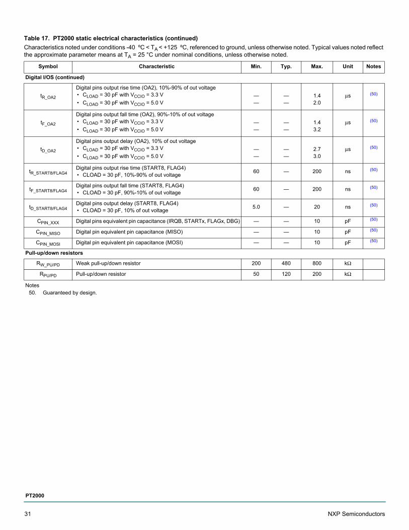
Digital I/OS (continued)
tR_OA2
Digital pins output rise time (OA2), 10%-90% of out voltage• CLOAD = 30 pF with VCCIO = 3.3 V
• CLOAD = 30 pF with VCCIO = 5.0 V——
——
1.42.0
μs (50)
tF_OA2
Digital pins output fall time (OA2), 90%-10% of out voltage• CLOAD = 30 pF with VCCIO = 3.3 V
• CLOAD = 30 pF with VCCIO = 5.0 V——
——
1.43.2
μs (50)
tD_OA2
Digital pins output delay (OA2), 10% of out voltage• CLOAD = 30 pF with VCCIO = 3.3 V
• CLOAD = 30 pF with VCCIO = 5.0 V——
——
2.73.0
μs (50)
tR_START8/FLAG4Digital pins output rise time (START8, FLAG4)• CLOAD = 30 pF, 10%-90% of out voltage
60 — 200 ns (50)
tF_START8/FLAG4Digital pins output fall time (START8, FLAG4)• CLOAD = 30 pF, 90%-10% of out voltage
60 — 200 ns (50)
tD_START8/FLAG4Digital pins output delay (START8, FLAG4)• CLOAD = 30 pF, 10% of out voltage
5.0 — 20 ns (50)
CPIN_XXX Digital pins equivalent pin capacitance (IRQB, STARTx, FLAGx, DBG) — — 10 pF (50)
CPIN_MISO Digital pin equivalent pin capacitance (MISO) — — 10 pF (50)
CPIN_MOSI Digital pin equivalent pin capacitance (MOSI) — — 10 pF (50)
Pull-up/down resistors
RW_PU/PD Weak pull-up/down resistor 200 480 800 kΩ
RPU/PD Pull-up/down resistor 50 120 200 kΩ
Notes50. Guaranteed by design.
Table 17. PT2000 static electrical characteristics (continued)
Characteristics noted under conditions -40 ºC < TA < +125 ºC, referenced to ground, unless otherwise noted. Typical values noted reflect the approximate parameter means at TA = 25 °C under nominal conditions, unless otherwise noted.
Symbol Characteristic Min. Typ. Max. Unit Notes
31 NXP Semiconductors
PT2000
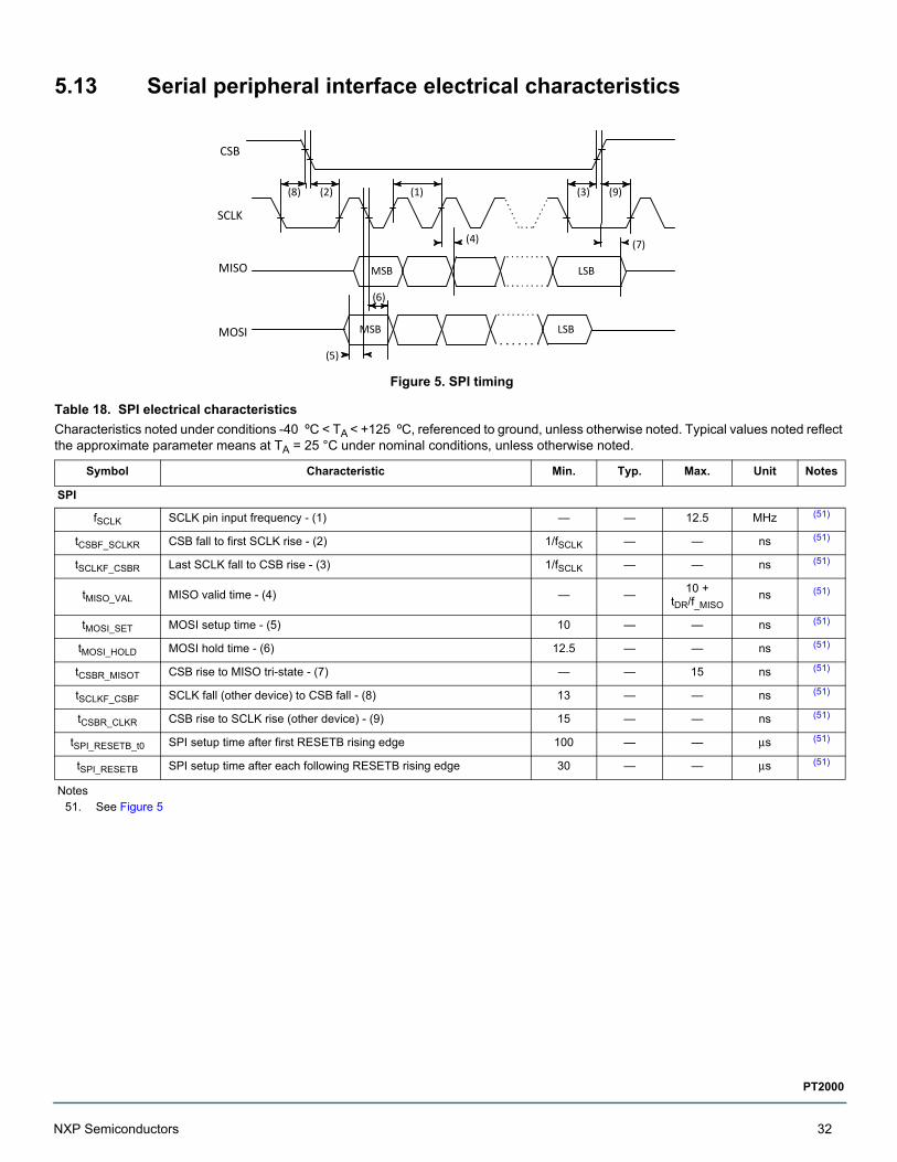
5.13 Serial peripheral interface electrical characteristics
Figure 5. SPI timing
Table 18. SPI electrical characteristics
Characteristics noted under conditions -40 ºC < TA < +125 ºC, referenced to ground, unless otherwise noted. Typical values noted reflect the approximate parameter means at TA = 25 °C under nominal conditions, unless otherwise noted.
Symbol Characteristic Min. Typ. Max. Unit Notes
SPI
fSCLK SCLK pin input frequency - (1) — — 12.5 MHz (51)
tCSBF_SCLKR CSB fall to first SCLK rise - (2) 1/fSCLK — — ns (51)
tSCLKF_CSBR Last SCLK fall to CSB rise - (3) 1/fSCLK — — ns (51)
tMISO_VAL MISO valid time - (4) — —10 +
tDR/f_MISOns (51)
tMOSI_SET MOSI setup time - (5) 10 — — ns (51)
tMOSI_HOLD MOSI hold time - (6) 12.5 — — ns (51)
tCSBR_MISOT CSB rise to MISO tri-state - (7) — — 15 ns (51)
tSCLKF_CSBF SCLK fall (other device) to CSB fall - (8) 13 — — ns (51)
tCSBR_CLKR CSB rise to SCLK rise (other device) - (9) 15 — — ns (51)
tSPI_RESETB_t0 SPI setup time after first RESETB rising edge 100 — — μs (51)
tSPI_RESETB SPI setup time after each following RESETB rising edge 30 — — μs (51)
Notes51. See Figure 5
CSB
SCLK
MISO
MOSI
(8) (2) (1) (3) (9)
(7)(4)
(6)
(5)
MSB
MSB LSB
LSB
NXP Semiconductors 32
PT2000
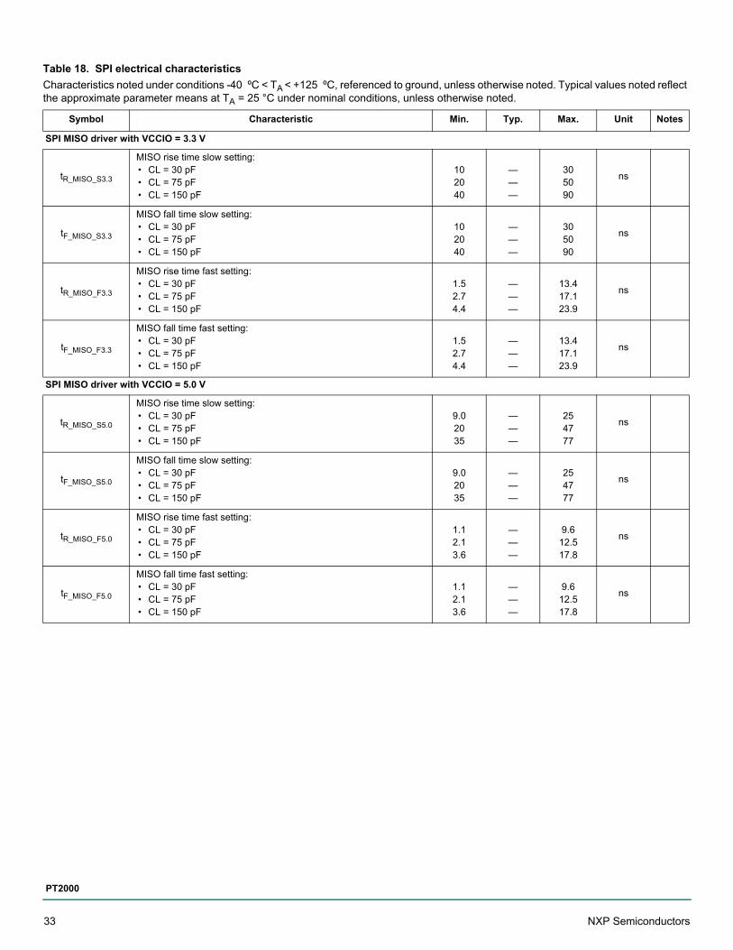
SPI MISO driver with VCCIO = 3.3 V
tR_MISO_S3.3
MISO rise time slow setting:• CL = 30 pF• CL = 75 pF• CL = 150 pF
102040
———
305090
ns
tF_MISO_S3.3
MISO fall time slow setting:• CL = 30 pF• CL = 75 pF• CL = 150 pF
102040
———
305090
ns
tR_MISO_F3.3
MISO rise time fast setting:• CL = 30 pF• CL = 75 pF• CL = 150 pF
1.52.74.4
———
13.417.123.9
ns
tF_MISO_F3.3
MISO fall time fast setting:• CL = 30 pF• CL = 75 pF• CL = 150 pF
1.52.74.4
———
13.417.123.9
ns
SPI MISO driver with VCCIO = 5.0 V
tR_MISO_S5.0
MISO rise time slow setting:• CL = 30 pF• CL = 75 pF• CL = 150 pF
9.02035
———
254777
ns
tF_MISO_S5.0
MISO fall time slow setting:• CL = 30 pF• CL = 75 pF• CL = 150 pF
9.02035
———
254777
ns
tR_MISO_F5.0
MISO rise time fast setting:• CL = 30 pF• CL = 75 pF• CL = 150 pF
1.12.13.6
———
9.612.517.8
ns
tF_MISO_F5.0
MISO fall time fast setting:• CL = 30 pF• CL = 75 pF• CL = 150 pF
1.12.13.6
———
9.612.517.8
ns
Table 18. SPI electrical characteristics
Characteristics noted under conditions -40 ºC < TA < +125 ºC, referenced to ground, unless otherwise noted. Typical values noted reflect the approximate parameter means at TA = 25 °C under nominal conditions, unless otherwise noted.
Symbol Characteristic Min. Typ. Max. Unit Notes
33 NXP Semiconductors
PT2000
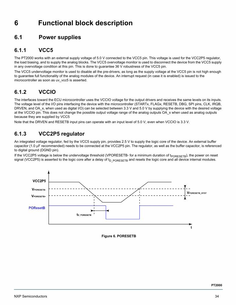
6 Functional block description
6.1 Power supplies
6.1.1 VCC5The PT2000 works with an external supply voltage of 5.0 V connected to the VCC5 pin. This voltage is used for the VCC2P5 regulator, the load biasing, and to supply the analog blocks. The VCC5 overvoltage monitor is used to disconnect the device from the VCC5 supply in any overvoltage condition at this pin. This is done to guarantee 36 V robustness of the VCC5 pin.
The VCC5 undervoltage monitor is used to disable all the pre-drivers, as long as the supply voltage at the VCC5 pin is not high enough to guarantee full functionality of the analog modules of the device. An interrupt request (in case it is enabled) is issued to the microcontroller as soon as uv_vcc5 is asserted.
6.1.2 VCCIOThe interfaces toward the ECU microcontroller uses the VCCIO voltage for the output drivers and receives the same levels on its inputs. The voltage level of the I/O pins interfacing the device with the microcontroller (STARTx, FLAGx, RESETB, DBG, SPI pins, CLK, IRQB, DRVEN, and OA_x, when used as digital I/O) can be selected between 3.3 V and 5.0 V by supplying the device with the desired voltage at the VCCIO pin. This does not change the possible output voltage range of the analog outputs OA_x when used as analog outputs because they are supplied by VCC5
Note that the DRVEN and RESETB input pins can operate with an input level of 5.0 V, even when VCCIO is 3.3 V.
6.1.3 VCC2P5 regulatorAn integrated voltage regulator, fed by the VCC5 supply pin, provides 2.5 V to supply the logic core of the device. An external buffer capacitor (1.0 μF recommended) needs to be connected at the VCC2P5 pin. The regulator, as well as the buffer capacitor, is referenced to digital ground (DGND pin).
If the VCC2P5 voltage is below the undervoltage threshold (VPORESETB- for a minimum duration of tPORESETB), the power on reset signal (VCC2P5) is asserted to the logic core after a delay of tD_PORESETB and resets the logic core and all device internal modules.
Figure 6. PORESETB
NXP Semiconductors 34
PT2000
6.1.4 VCCP regulator
6.1.4.1 Internal VCCP (vccp_ext_en='0')
The voltage source at the VBATT input pin provides power for the VCCP regulator. This integrated linear regulator provides typically 7.0 V at the VCCP pin, to supply the pre-driver section of the device. The regulator uses low drop out features to extend the system's operating range when VBATT temporarily falls below its normal operating range, for example during engine crank conditions. This avoids problems caused by insufficient gate voltage, such as slow MOSFET switching and increased on-state losses. A capacitor (4.7 μF recommended) is required at the VCCP pin to provide the high peak currents required when charging a MOSFET gate.
At low VCC5, the regulator may be active, but with an increased dropout voltage. The low dropout mode of the regulator is active only when the voltage at VCC5 is above the VCC5 undervoltage threshold VUVVCC5+.
If VCC5 is not present or low, POResetB is active and disables the VCCP regulator.
VCCP during bootstrap initialization:
1. If the DBG pin is not used as a digital I/O, the DBG pin logic level is ‘1’ during reset due to the device internal weak pull-up resistor. As result, the internal VCCP regulator is switched on during the HS pre-driver bootstrap initialization phase. (refer to See Power-up sequence VCCP and bootstrap capacitors on page 58).
2. If the DBG pin is used as a digital I/O. This means the DBG pin logic level is undefined during reset and may be '0'. As result, the internal VCCP regulator's On status during HS pre-driver bootstrap init phase can only be guaranteed if vccp_ext_en is set to '0'. The bit has to be configured as soon as possible during device init, to start the pre-charging of the bootstrap capacitors soon enough (refer to Table 148, Driver_config_Part 2 (1A6h)).
Note that this regulator also needs a charge pump voltage coming from the VBOOST pin. Due to this, the VCCP regulator is not functional when the voltage on the VBOOST pin is below 4.7 V.
6.1.4.2 External VCCP (vccp_ext_en='1')
The VCCP can also be powered by an external voltage source connected to the VCCP pin. The internal VCCP regulator is sized for 12 V system operation, including the ISO voltage transients specified for those systems. But for 24 V system operation, the internal VCCP linear regulator dissipates too much power. In this case, the internal VCCP regulator should be switched off by setting the vccp_ext_en bit of the driver_config_part2 register (1A6h) to '1' and an external regulator needs to be used.
VCCP during initialization VCCP:
1. If is not possible to turn on the internal VCCP regulator for a limited time in parallel to the external voltage source, the DBG pin has
to be tied to logic level '0' and the SPI configuration bit has to stay at '1', to strictly avoid the internal regulator to be switched on at any time. The logic level of the DBG pin should be forced by a pull-down resistor towards GND.
2. On the other hand, if it is possible to switch on the internal regulator for some limited time in parallel with the external voltage supply without destroying it, no special measures have to be taken during startup. After bootstrap initialization, the vccp_ext_en bit has to be set to '1' (refer to Table 148, Driver_config_Part 2 (1A6h)).
6.1.4.3 VCCP undervoltage
VCCP voltage is internally monitored by a voltage comparator to detect if it is in the operating range. In case of an undervoltage when falling below the lower threshold, the gate driver outputs are switched off by the digital core.
This prevents possible malfunctions and/or failures: in case of an undervoltage, operations are stopped before any malfunction, due to insufficient gate driver supply voltage. Moreover, in case of a battery voltage disconnection, all MOSFETs are switched off (and therefore inductive loads are disconnected) before the electrolytic capacitors on the VBATT line are completely discharged. This prevents any negative voltage on the VBATT line, which may cause failures on the VBATT, VCCP, D_HSx and B_HSx pins due to exceeding its maximum ratings.
35 NXP Semiconductors
PT2000
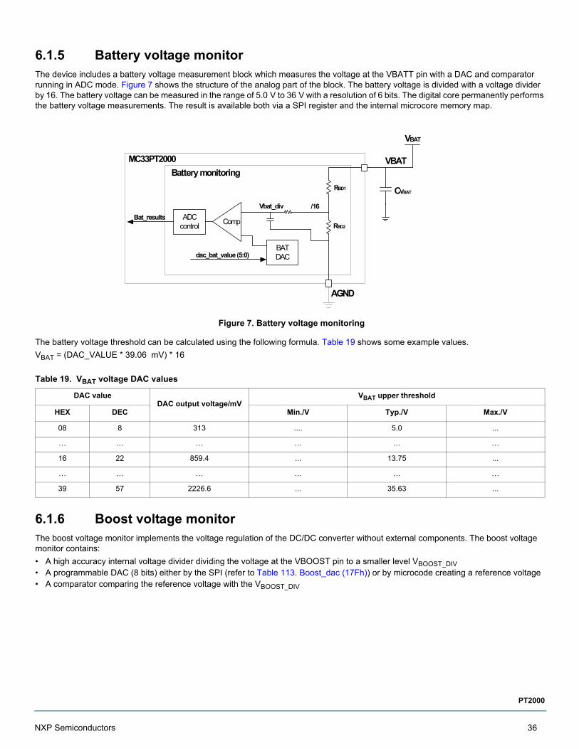
6.1.5 Battery voltage monitor The device includes a battery voltage measurement block which measures the voltage at the VBATT pin with a DAC and comparator running in ADC mode. Figure 7 shows the structure of the analog part of the block. The battery voltage is divided with a voltage divider by 16. The battery voltage can be measured in the range of 5.0 V to 36 V with a resolution of 6 bits. The digital core permanently performs the battery voltage measurements. The result is available both via a SPI register and the internal microcore memory map.
Figure 7. Battery voltage monitoring
The battery voltage threshold can be calculated using the following formula. Table 19 shows some example values.
VBAT = (DAC_VALUE * 39.06 mV) * 16
6.1.6 Boost voltage monitorThe boost voltage monitor implements the voltage regulation of the DC/DC converter without external components. The boost voltage monitor contains:
• A high accuracy internal voltage divider dividing the voltage at the VBOOST pin to a smaller level VBOOST_DIV• A programmable DAC (8 bits) either by the SPI (refer to Table 113. Boost_dac (17Fh)) or by microcode creating a reference voltage• A comparator comparing the reference voltage with the VBOOST_DIV
Table 19. VBAT voltage DAC values
DAC valueDAC output voltage/mV
VBAT upper threshold
HEX DEC Min./V Typ./V Max./V
08 8 313 .... 5.0 ...
… … … … … …
16 22 859.4 ... 13.75 ...
… … … … … …
39 57 2226.6 ... 35.63 ...
BAT DAC
CompADC
controlBat_results
dac_bat_value (5:0)
Vbat_div /16
VBAT
AGND
MC33PT2000
Battery monitoring
RBD1
RBD2
VBAT
CVBAT
NXP Semiconductors 36
PT2000
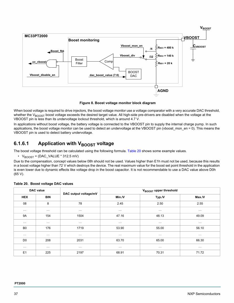
Figure 8. Boost voltage monitor block diagram
When boost voltage is required to drive injectors, the boost voltage monitor use a voltage comparator with a very accurate DAC threshold, whether the VBOOST boost voltage exceeds the desired target value. All high-side pre-drivers are disabled when the voltage at the VBOOST pin is less than its undervoltage lockout threshold, which is around 4.7 V.
In applications without boost voltage, the battery voltage is connected to the VBOOST pin to supply the internal charge pump. In such applications, the boost voltage monitor can be used to detect an undervoltage at the VBOOST pin (vboost_mon_en = 0). This means the VBOOST pin is used to detect battery undervoltage.
6.1.6.1 Application with VBOOST voltage
The boost voltage threshold can be calculated using the following formula. Table 20 shows some example values.
• VBOOST = (DAC_VALUE * 312.5 mV)
Due to the compensation, concept values below 08h should not be used. Values higher than E1h must not be used, because this results in a boost voltage higher than 72 V which destroys the device. The real maximum value for the boost set point threshold in the application is even lower due to dynamic effects like voltage drop in the boost capacitor. It is not recommendable to use a DAC value above D0h (65 V).
Table 20. Boost voltage DAC values
DAC valueDAC output voltage/mV
VBOOST upper threshold
HEX BIN Min./V Typ./V Max./V
08 8 78 2.45 2.50 2.55
… … … … … …
9A 154 1504 47.16 48.13 49.09
… … … … … …
B0 176 1719 53.90 55.00 56.10
… … … … … …
D0 208 2031 63.70 65.00 66.30
… … … … … …
E1 225 2197 68.91 70.31 71.72
BOOST DAC
CompBoostFilter
Vboost_disable_en
uv_vboost
Boost_fbk
dac_boost_value (7:0)
Vboost_mon_en
Vboost_div
/4
/32
VBOOST
AGND
MC33PT2000Boost monitoring
RBD3 = 480 k
RBD2 = 140 k
RBD1 = 20 k
VBOOST
CVBOOST
37 NXP Semiconductors
PT2000
6.1.6.2 Application without boost voltage
For this purpose, it is possible to change the internal voltage divider ratio from 1/32 to 1/4 by setting the signal boost_mon_en high. To detect undervoltage and use the signal uv_vboost to disable the pre-drivers, the uv_vboost bit needs to be set to “1” (refer to Table 162, driver_status (1B2h)). The uv_vboost signal goes high as soon as the voltage at the VBOOST pin is below the threshold, if the VBOOST UV monitor is enabled (uv_vboost_en =1).
The same digital filter used for the VBOOST voltage measurement is also used for the VBOOST UV monitoring mode. The DAC set point value in this mode has to be chosen to fulfill two requirements:
• The pre-drivers must not be disabled at a battery voltage above 5.0 V • The device internal charge pump only works properly down to a battery voltage of 4.7 V
The VBOOST UV threshold can be calculated using the following formula.
• VBOOST = (DAC_VALUE * 39.1 mV)
6.1.7 Charge pumpThe PT2000 provides one charge pump with independent outputs for each of the seven high-side drivers. The independent outputs allow complete flexibility of the topology used, meaning all high-sides can drive MOSFETs with the drain connected to VBOOST or VBAT. But there is a limitation on the diagnostics only HS2, 4, and 6 can use the VBOOST for monitoring (for example, VBAT or VBOOST).
In most operating topologies and conditions, the bootstrap is the primary source of charge for the bootstrap capacitor, and the charge pump sustains the voltage at each bootstrap capacitor when it is not being charged by low-side switching.
This charge pump allows 100% duty cycle operation of the high-side MOSFETs while the bootstrap circuitry is not operating (VS_HSx voltage never goes significantly below the VCCP voltage). In this condition, the charge pump provides current maintaining each bootstrap capacitor charged via independent current sources, to guarantee a minimum VGS voltage.
The charge pump, supplied by VBOOST, creates gate drive voltages of about 8.0 V greater than the voltage at VBOOST. However, their current capacity is sufficient only for low frequency switching. The charge pump is not running as long as the POResetB reset signal is active.
The internal CP can be used to charge the bootstrap capacitors during init with a guaranteed current of 20 μA per HS pre-driver. This current is only available if there is no leakage current from B_HSx pin. Any possible leakage current has to be subtracted from this available charge current (See Using the charge pump to charge bootstrap capacitors on page 59).
6.2 Clock subsystem
The digital logic is supplied by a clock (cksys) generated by the PLL from the 1.0 MHz clock forced externally on CLK pin. Two internal clocks are derived from the PLL:
• the main logic clock cksys• the code RAM clock cksys_cram inverted in respect to cksys• the Data RAM clock cksys_dram inverted in respect to cksys
If an unsuitable signal is applied on the CLK pin, the device automatically switches to the internal backup clock. The PLL output frequency can be modulated for EMC purposes. Modulation activation is enabled by default, but can be disabled by the SPI. Refer to Table 151 PLL_Config (1A7h).
NXP Semiconductors 38
PT2000
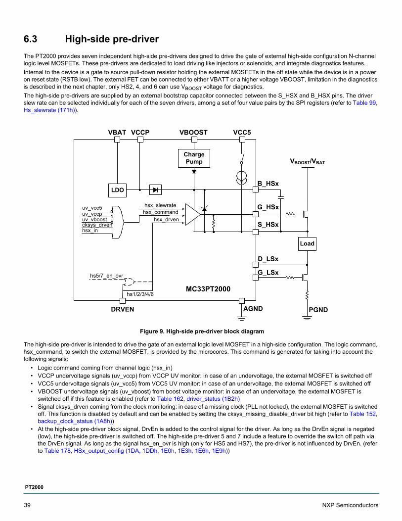
6.3 High-side pre-driver
The PT2000 provides seven independent high-side pre-drivers designed to drive the gate of external high-side configuration N-channel logic level MOSFETs. These pre-drivers are dedicated to load driving like injectors or solenoids, and integrate diagnostics features.
Internal to the device is a gate to source pull-down resistor holding the external MOSFETs in the off state while the device is in a power on reset state (RSTB low). The external FET can be connected to either VBATT or a higher voltage VBOOST, limitation in the diagnostics is described in the next chapter, only HS2, 4, and 6 can use VBOOST voltage for diagnostics.
The high-side pre-drivers are supplied by an external bootstrap capacitor connected between the S_HSX and B_HSX pins. The driver slew rate can be selected individually for each of the seven drivers, among a set of four value pairs by the SPI registers (refer to Table 99, Hs_slewrate (171h)).
Figure 9. High-side pre-driver block diagram
The high-side pre-driver is intended to drive the gate of an external logic level MOSFET in a high-side configuration. The logic command, hsx_command, to switch the external MOSFET, is provided by the microcores. This command is generated for taking into account the following signals:
• Logic command coming from channel logic (hsx_in)• VCCP undervoltage signals (uv_vccp) from VCCP UV monitor: in case of an undervoltage, the external MOSFET is switched off• VCC5 undervoltage signals (uv_vcc5) from VCC5 UV monitor: in case of an undervoltage, the external MOSFET is switched off• VBOOST undervoltage signals (uv_vboost) from boost voltage monitor: in case of an undervoltage, the external MOSFET is
switched off if this feature is enabled (refer to Table 162, driver_status (1B2h)• Signal cksys_drven coming from the clock monitoring: in case of a missing clock (PLL not locked), the external MOSFET is switched
off. This function is disabled by default and can be enabled by setting the cksys_missing_disable_driver bit high (refer to Table 152, backup_clock_status (1A8h))
• At the high-side pre-driver block signal, DrvEn is added to the control signal for the driver. As long as the DrvEn signal is negated (low), the high-side pre-driver is switched off. The high-side pre-driver 5 and 7 include a feature to override the switch off path via the DrvEn signal. As long as the signal hsx_en_ovr is high (only for HS5 and HS7), the pre-driver is not influenced by DrvEn. (refer to Table 178, HSx_output_config (1DA, 1DDh, 1E0h, 1E3h, 1E6h, 1E9h))
Charge Pump
LDO
Load
AGNDDRVEN
D_LSx
G_LSx
VBOOST/VBAT
B_HSx
G_HSx
S_HSx
VCC5VBOOSTVCCPVBAT
uv_vcc5uv_vccpuv_vboostcksys_drvenhsx_in
hsx_slewratehsx_command
hsx_drven
hs5/7_en_ovr
MC33PT2000
PGND
hs1/2/3/4/6
39 NXP Semiconductors
PT2000
The truth table describing the status of hsx_command signal is given in Figure 21.
The pre-driver G_HSx output is set according to hsx_command:
• When the hsx_command is high, the G_HSx pin is driven high (pull-up to B_HSx voltage);• When the hsx_command is low, the G_HSx pin is driven low (pull-down to S_HSx voltage).
6.3.1 High-side pre-driver slew rate controlThe driver strength can be selected individually for each of the drivers among a set of values by the SPI registers. There are four selectable driver strengths. The strength for the rising and falling edge can be chosen individually for each driver. Changing the rising edge affects the falling edge such as to retain the same absolute slew rate. The given value of voltage slew rate is only an indication and is dependent on the used MOSFET and the additional gate circuit (refer to Slew rate high-side and low-side selection register).
6.3.2 Safe state of high-side pre-driverWhen reset (RSTB) is asserted or DRV_EN is negated, the G_HSx output is immediately forced to a low level, thus switching off the external MOSFET, to guarantee a safe condition while the device is not operating. In addition to this, an integrated pull-down resistor RPD_HSX between G_HSx and S_HSx of about 1.0 MΩ keeps the external MOSFET in the off state even when the bootstrap voltage is low.
Table 21. High-side pre-driver truth table
DRV_EN hs5/7_en_ovr uv_vccp uv_vcc5 uv_vboost cksys_drven hsx_in hsx_command Driver status
0 - - - - - - 0 off
- - 1 - - - - 0 off
- - - 1 - - - 0 off
- - - - 1 - - 0 off
- - - - - 0 - 0 off
- - - - - - 0 0 off
0 1 0 0 0 1 1 1on (hs5/7) / off
(other hsx)
1 - 0 0 0 1 1 1 on
Table 22. Slew rate settings for HS pre-drivers
hsx_slewrate(1:0) Slew-rate/ V/µSRDS(ON)_PMOS
(switching on)/ΩRDS(ON)_NMOS
(switching off)/Ω
00 300 14.6 5.9
01 50 85 35
10 25 169 69
11 12.5 337 138
NXP Semiconductors 40
PT2000
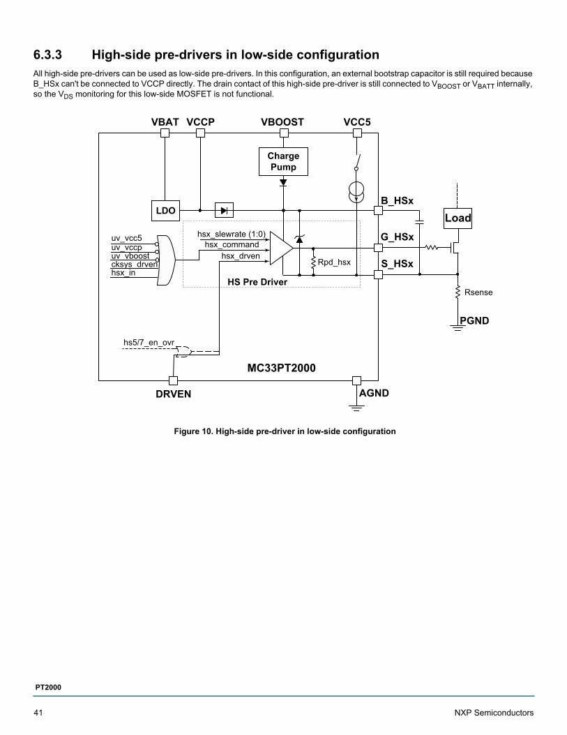
6.3.3 High-side pre-drivers in low-side configurationAll high-side pre-drivers can be used as low-side pre-drivers. In this configuration, an external bootstrap capacitor is still required because B_HSx can't be connected to VCCP directly. The drain contact of this high-side pre-driver is still connected to VBOOST or VBATT internally, so the VDS monitoring for this low-side MOSFET is not functional.
Figure 10. High-side pre-driver in low-side configuration
ChargePump
LDOLoad
AGNDDRVEN
B_HSx
G_HSx
S_HSx
VCC5VBOOSTVCCPVBAT
uv_vcc5uv_vccpuv_vboostcksys_drvenhsx_in
hsx_slewrate (1:0)hsx_command
hsx_drven
hs5/7_en_ovr
MC33PT2000
PGND
RsenseHS Pre Driver
Rpd_hsx
41 NXP Semiconductors
PT2000
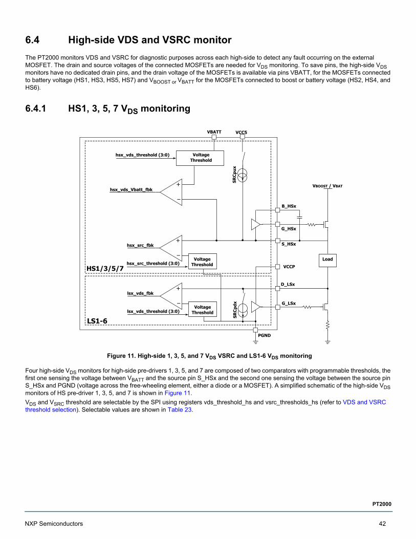
6.4 High-side VDS and VSRC monitor
The PT2000 monitors VDS and VSRC for diagnostic purposes across each high-side to detect any fault occurring on the external MOSFET. The drain and source voltages of the connected MOSFETs are needed for VDS monitoring. To save pins, the high-side VDS monitors have no dedicated drain pins, and the drain voltage of the MOSFETs is available via pins VBATT, for the MOSFETs connected to battery voltage (HS1, HS3, HS5, HS7) and VBOOST or VBATT for the MOSFETs connected to boost or battery voltage (HS2, HS4, and HS6).
6.4.1 HS1, 3, 5, 7 VDS monitoring
Figure 11. High-side 1, 3, 5, and 7 VDS VSRC and LS1-6 VDS monitoring
Four high-side VDS monitors for high-side pre-drivers 1, 3, 5, and 7 are composed of two comparators with programmable thresholds, the first one sensing the voltage between VBATT and the source pin S_HSx and the second one sensing the voltage between the source pin S_HSx and PGND (voltage across the free-wheeling element, either a diode or a MOSFET). A simplified schematic of the high-side VDS monitors of HS pre-driver 1, 3, 5, and 7 is shown in Figure 11.
VDS and VSRC threshold are selectable by the SPI using registers vds_threshold_hs and vsrc_thresholds_hs (refer to VDS and VSRC threshold selection). Selectable values are shown in Table 23.
VBATT
G_LSx
VCCP
lsx_vds_threshold (3:0)
PGND
Load
D_LSx
Voltage Threshold
lsx_vds_fbk
B_HSx
G_HSx
S_HSx
VBOOST / VBAT
hsx_vds_threshold (3:0) Voltage Threshold
hsx_src_threshold (3:0)Voltage
Threshold
hsx_src_fbk+
–
+
–
VCC5
SRC
pux
SRC
pdx
hsx_vds_Vbatt_fbk+
–
HS1/3/5/7
LS1-6
NXP Semiconductors 42
PT2000
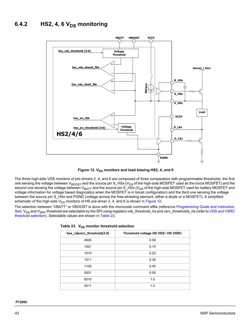
6.4.2 HS2, 4, 6 VDS monitoring
Figure 12. VDS monitors and load biasing HS2, 4, and 6
The three high-side VDS monitors of pre-drivers 2, 4, and 6 are composed of three comparators with programmable thresholds, the first one sensing the voltage between VBOOST and the source pin S_HSx (VDS of the high-side MOSFET used as the boost MOSFET) and the second one sensing the voltage between VBATT and the source pin S_HSx (VDS of the high-side MOSFET used for battery MOSFET and voltage information for voltage based diagnostics when the MOSFET is in boost configuration) and the third one sensing the voltage between the source pin S_HSx and PGND (voltage across the free-wheeling element, either a diode or a MOSFET). A simplified schematic of the high-side VDS monitors of HS pre-driver 2, 4, and 6 is shown in Figure 12.
The selection between “VBATT” or VBOOST is done with the microcode command slfbk (reference Programming Guide and Instruction Set). VDS and VSRC threshold are selectable by the SPI using registers vds_threshold_hs and vsrc_thresholds_hs (refer to VDS and VSRC threshold selection). Selectable values are shown in Table 23.
Table 23. VDS monitor threshold selection
hsx_vds/src_threshold(3:0) Threshold voltage HS VDS / HS VSRC
0000 0.00
1001 0.10
1010 0.20
1011 0.30
1100 0.40
0001 0.50
0010 1.0
0011 1.5
VBATT
G_LSx
VCCP
PGND
Load
D_LSx
B_HSx
G_HSx
S_HSx
VBOOST / VBAT
hsx_vds_threshold (3:0) Voltage Threshold
hsx_vds_vbatt_fbk
hsx_src_threshold (3:0) Voltage Threshold
hsx_src_fbk
+
–
+
–
VCC5
SRC
pux
VBOOST
hsx_vds_vboost_fbk+
–
HS2/4/6
43 NXP Semiconductors
PT2000

The high-side VDS comparator compares VDS of the high-side MOSFET, acquired through VBOOST, VBATT, and the S_HSx pins, with the selected threshold. In actual implementation, the selected threshold voltage is subtracted to the VBOOST or VBATT voltage and compared to the S_HSx voltage.
The high-side VSRC comparator compares the voltage across the freewheeling element, acquired through the S_HSx pins and PGND, with the selected threshold. In actual implementation, the selected threshold voltage is added to PGND voltage and compared to the S_HSx voltage.
6.5 Low-side pre-driver (LS1-6)
There are six general purpose low-side pre-drivers and all drive external N-Channel logic level type power MOSFETs used in low-side configurations.
Figure 13. Low-side pre-driver block diagram
Internal to the device, a gate to source pull-down resistor RPD_LSX holds the external MOSFETs in the off state, while the device is in a power on reset state (RSTB low).
The low-side pre-drivers are supplied by VCCP voltage. The low-side pre-driver is intended to drive the gate of an external logic level MOSFET in low-side configuration. The logic command lsx_command, to switch the external MOSFET, is provided by the digital block. This command is generated, taking into account the following signals:
• Logic command coming from channel logic (lsx_in).• VCCP undervoltage signals (uv_vccp) from the VCCP UV monitor: In case of an undervoltage, the external MOSFET is switched off.• VCC5 undervoltage signals (uv_vcc5) from VCC5 UV monitor: In case of an undervoltage the external MOSFET is switched off.
0100 2.0
0101 2.5
0110 3.0
0111 3.5
Table 23. VDS monitor threshold selection (continued)
hsx_vds/src_threshold(3:0) Threshold voltage HS VDS / HS VSRC
LDO
Load
PGNDDRVEN
D_LSx
G_LSx
VCCPVBAT
uv_vcc5
uv_vccpcksys_drvenlsx_in
lsx_slewrate (1:0)lsx_command
lsx_drven
ls6_en_ovr
MC33PT2000
PGND
RSENSE
LS Pre-driver
Rpd_lsx
other lsx
NXP Semiconductors 44
PT2000
• Signal cksys_drven coming from the clock monitoring: In case of a missing clock (PLL not locked), the external MOSFET is switched off. This function is disabled by default and can be enabled by setting the cksys_missing_disable_driver bit high (refer to Table 152, backup_clock_status (1A8h)).
• For safety purpose DRV_EN is added to the control signal for the driver. As long as DRV_EN signal is negated (low) the low-side pre-driver is switched off. The low-side pre-driver 6 includes a feature to override the switch off path via the DRV_EN signal (refer to Table 174, LSx_output_config (1C2h, 1C5h,1C8h, 1CBh, 1CEh, 1D1h)).
The truth table describing the status of lsx_command signal is given in Table 24.
The pre-driver G_LSx output is set according to lsx_command:
• When lsx_cmd is high, the G_LSx pin is driven high (pull-up to VCCP voltage)• When lsx_cmd is low, the G_LSx pin is driven low (pull-down to PGND voltage)
6.5.1 Low-side pre-driver slew rate controlAll low-side pre-drivers feature a programmable slew-rate control. The settings can be changed independently for each pre-driver by the signals lsx_slewrate(1:0) coming from the digital core. The given value of voltage slew-rate is only an indication and is dependant on the used MOSFET and the additional gate circuit.(refer to Slew rate high-side and low-side selection register).
Table 24. Low-side pre-driver truth table
DRV_EN ls6_en_ovr uv_vccp uv_vcc5 cksys_drven lsx_in lsx_command Driver Status
0 - - - - - 0 off
- - 1 - - - 0 off
- - - 1 - - 0 off
- - - - 0 - 0 off
- - - - - 0 0 off
- 1 0 0 1 1 1 on
1 - 0 0 1 1 1 on
Table 25. Slew rate settings for LS pre-drivers 1-6
lsx_slewrate(1:0) Slew-rate/ V/µSRDS(ON)_PMOS (switching
on)/ΩRDS(ON)_NMOS (switching
off)/Ω
00 300 14.6 5.9
01 50 84 35
10 25 170 69
11 12.5 337 138
45 NXP Semiconductors
PT2000

6.5.2 LS1 - LS6 VDS monitor
Figure 14. VDS monitoring LS1 to LS6
For VDS monitoring of the external low-side MOSFET, a comparator with programmable threshold is provided, sensing the voltage between the drain pin D_LSx and PGND (VDS of the low-side MOSFET). If a sense resistor is connected between the low-side MOSFET and ground, the voltage drop on the resistor is included in the measurement. VDS threshold are selectable by the SPI using vds_threshold_ls registers (refer to Table 96, Vds_threshold_ls_Part 1 (16Fh)) and Table 97, Vds_threshold_ls_Part 2 (170h)). Selectable values are shown in Table 26.
Table 26. Low-side VDS monitor threshold selection
lsx_vds _threshold(3:0) Threshold Voltage LS VDS
0000 0.00
1001 0.10
1010 0.20
1011 0.30
1100 0.40
0001 0.50
0010 1.0
0011 1.5
0100 2.0
0101 2.5
0110 3.0
0111 3.5
G_LSx
VCCP
lsx_vds_threshold (3:0)
PGND
Load
D_LSx
Voltage Threshold
lsx_vds_fbk+
–
SRC
pdx
LS1-6
NXP Semiconductors 46
PT2000
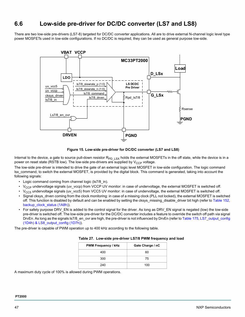
6.6 Low-side pre-driver for DC/DC converter (LS7 and LS8)
There are two low-side pre-drivers (LS7-8) targeted for DC/DC converter applications. All are to drive external N-channel logic level type power MOSFETs used in low-side configurations. If no DC/DC is required, they can be used as general purpose low-side.
Figure 15. Low-side pre-driver for DC/DC converter (LS7 and LS8)
Internal to the device, a gate to source pull-down resistor RPD_LSX holds the external MOSFETs in the off state, while the device is in a power on reset state (RSTB low). The low-side pre-drivers are supplied by VCCP voltage.
The low-side pre-driver is intended to drive the gate of an external logic level MOSFET in low-side configuration. The logic command lsx_command, to switch the external MOSFET, is provided by the digital block. This command is generated, taking into account the following signals:
• Logic command coming from channel logic (ls7/8_in).• VCCP undervoltage signals (uv_vccp) from VCCP UV monitor: in case of undervoltage, the external MOSFET is switched off. • VCC5 undervoltage signals (uv_vcc5) from VCC5 UV monitor: in case of undervoltage, the external MOSFET is switched off. • Signal cksys_drven coming from the clock monitoring: in case of a missing clock (PLL not locked), the external MOSFET is switched
off. This function is disabled by default and can be enabled by setting the cksys_missing_disable_driver bit high (refer to Table 152, backup_clock_status (1A8h)).
• For safety purpose DRV_EN is added to the control signal for the driver. As long as DRV_EN signal is negated (low) the low-side pre-driver is switched off. The low-side pre-driver for the DC/DC converter includes a feature to override the switch off path via signal DrvEn. As long as the signals ls7/8_en_ovr are high, the pre-driver is not influenced by DrvEn (refer to Table 175, LS7_output_config (1D4h) & LS8_output_config (1D7h)).
The pre-driver is capable of PWM operation up to 400 kHz according to the following table.
A maximum duty cycle of 100% is allowed during PWM operations.
Table 27. Low-side pre-driver LS7/8 PWM frequency and load
PWM Frequency / kHz Gate Charge / nC
400 60
300 75
240 100
LDO
Load
PGNDDRVEN
D_LSx
G_LSx
VCCPVBAT
uv_vcc5uv_vccpcksys_drvenls7/8_in
ls7/8_slewrate_n (1:0)ls7/8_command
ls7/8_drven
Ls7/8_en_ovr
MC33PT2000
PGND
Rsense
ls7/8_slewrate_p (1:0)
Rpd_ls7/8
LS DCDCPre Driver
47 NXP Semiconductors
PT2000
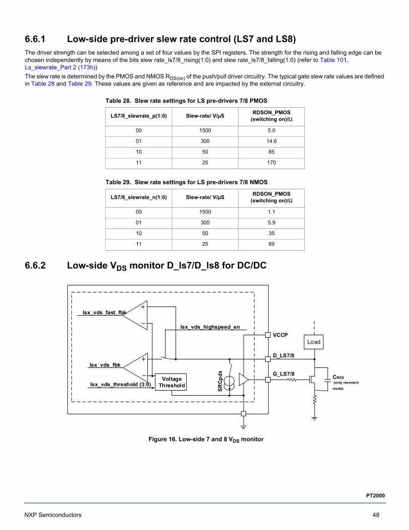
6.6.1 Low-side pre-driver slew rate control (LS7 and LS8)The driver strength can be selected among a set of four values by the SPI registers. The strength for the rising and falling edge can be chosen independently by means of the bits slew rate_ls7/8_rising(1:0) and slew rate_ls7/8_falling(1:0) (refer to Table 101, Ls_slewrate_Part 2 (173h))
The slew rate is determined by the PMOS and NMOS RDS(on) of the push/pull driver circuitry. The typical gate slew rate values are defined in Table 28 and Table 29. These values are given as reference and are impacted by the external circuitry.
6.6.2 Low-side VDS monitor D_ls7/D_ls8 for DC/DC
Figure 16. Low-side 7 and 8 VDS monitor
Table 28. Slew rate settings for LS pre-drivers 7/8 PMOS
LS7/8_slewrate_p(1:0) Slew-rate/ V/µSRDSON_PMOS
(switching on)/Ω
00 1500 5.0
01 300 14.6
10 50 85
11 25 170
Table 29. Slew rate settings for LS pre-drivers 7/8 NMOS
LS7/8_slewrate_n(1:0) Slew-rate/ V/µSRDSON_PMOS
(switching on)/Ω
00 1500 1.1
01 300 5.9
10 50 35
11 25 69
Load
lsx_vds_fast_fbk
lsx_vds_highspeed_en
lsx_vds_threshold (3:0)
lsx_vds_fbk
VoltageThreshold
SRCp
dx
VCCP
D_LS7/8
G_LS7/8 CRES (only resonant mode)
NXP Semiconductors 48
PT2000
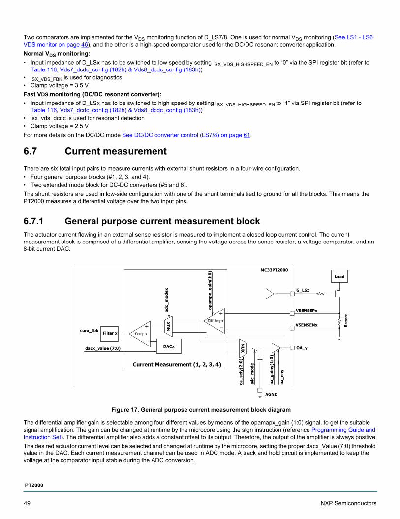
Two comparators are implemented for the VDS monitoring function of D_LS7/8. One is used for normal VDS monitoring (See LS1 - LS6 VDS monitor on page 46), and the other is a high-speed comparator used for the DC/DC resonant converter application.
Normal VDS monitoring:
• Input impedance of D_LSx has to be switched to low speed by setting lSX_VDS_HIGHSPEED_EN to “0” via the SPI register bit (refer to Table 116, Vds7_dcdc_config (182h) & Vds8_dcdc_config (183h))
• lSX_VDS_FBK is used for diagnostics• Clamp voltage = 3.5 V
Fast VDS monitoring (DC/DC resonant converter):
• Input impedance of D_LSx has to be switched to high speed by setting lSX_VDS_HIGHSPEED_EN to “1” via SPI register bit (refer to Table 116, Vds7_dcdc_config (182h) & Vds8_dcdc_config (183h))
• lsx_vds_dcdc is used for resonant detection• Clamp voltage = 2.5 V
For more details on the DC/DC mode See DC/DC converter control (LS7/8) on page 61.
6.7 Current measurement
There are six total input pairs to measure currents with external shunt resistors in a four-wire configuration.
• Four general purpose blocks (#1, 2, 3, and 4).• Two extended mode block for DC-DC converters (#5 and 6).
The shunt resistors are used in low-side configuration with one of the shunt terminals tied to ground for all the blocks. This means the PT2000 measures a differential voltage over the two input pins.
6.7.1 General purpose current measurement blockThe actuator current flowing in an external sense resistor is measured to implement a closed loop current control. The current measurement block is comprised of a differential amplifier, sensing the voltage across the sense resistor, a voltage comparator, and an 8-bit current DAC.
Figure 17. General purpose current measurement block diagram
The differential amplifier gain is selectable among four different values by means of the opamapx_gain (1:0) signal, to get the suitable signal amplification. The gain can be changed at runtime by the microcore using the stgn instruction (reference Programming Guide and Instruction Set). The differential amplifier also adds a constant offset to its output. Therefore, the output of the amplifier is always positive.
The desired actuator current level can be selected and changed at runtime by the microcore, setting the proper dacx_Value (7:0) threshold value in the DAC. Each current measurement channel can be used in ADC mode. A track and hold circuit is implemented to keep the voltage at the comparator input stable during the ADC conversion.
G_LSz
oa_
sely
(2:0
)
Load
OA_ydacx_value (7:0)
+
–
VSENSEPx
VSENSENx+
–DACx
curx_fbk
adc_
mod
ex
AGND
opam
px_
gain
(1:0
)
adc_
mod
e
oa_
gain
y(1
:0)
oa_
eny
RSE
NSE
X
Filter x
Current Measurement (1, 2, 3, 4)
MU
X
MU
X
MC33PT2000
Diff Ampx
Comp x
49 NXP Semiconductors
PT2000
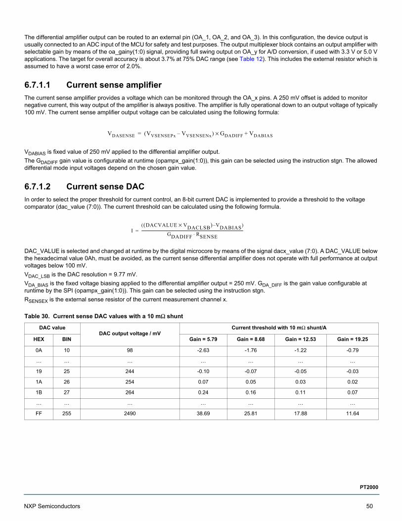
The differential amplifier output can be routed to an external pin (OA_1, OA_2, and OA_3). In this configuration, the device output is usually connected to an ADC input of the MCU for safety and test purposes. The output multiplexer block contains an output amplifier with selectable gain by means of the oa_gainy(1:0) signal, providing full swing output on OA_y for A/D conversion, if used with 3.3 V or 5.0 V applications. The target for overall accuracy is about 3.7% at 75% DAC range (see Table 12). This includes the external resistor which is assumed to have a worst case error of 2.0%.
6.7.1.1 Current sense amplifier
The current sense amplifier provides a voltage which can be monitored through the OA_x pins. A 250 mV offset is added to monitor negative current, this way output of the amplifier is always positive. The amplifier is fully operational down to an output voltage of typically 100 mV. The current sense amplifier output voltage can be calculated using the following formula:
VDABIAS is fixed value of 250 mV applied to the differential amplifier output.
The GDADIFF gain value is configurable at runtime (opampx_gain(1:0)), this gain can be selected using the instruction stgn. The allowed differential mode input voltages depend on the chosen gain value.
6.7.1.2 Current sense DAC
In order to select the proper threshold for current control, an 8-bit current DAC is implemented to provide a threshold to the voltage comparator (dac_value (7:0)). The current threshold can be calculated using the following formula.
DAC_VALUE is selected and changed at runtime by the digital microcore by means of the signal dacx_value (7:0). A DAC_VALUE below the hexadecimal value 0Ah, must be avoided, as the current sense differential amplifier does not operate with full performance at output voltages below 100 mV.
VDAC_LSB is the DAC resolution = 9.77 mV.
VDA_BIAS is the fixed voltage biasing applied to the differential amplifier output = 250 mV. GDA_DIFF is the gain value configurable at runtime by the SPI (opampx_gain(1:0)). This gain can be selected using the instruction stgn.
RSENSEX is the external sense resistor of the current measurement channel x.
Table 30. Current sense DAC values with a 10 mΩ shunt
DAC valueDAC output voltage / mV
Current threshold with 10 mΩ shunt/A
HEX BIN Gain = 5.79 Gain = 8.68 Gain = 12.53 Gain = 19.25
0A 10 98 -2.63 -1.76 -1.22 -0.79
… … … … … … …
19 25 244 -0.10 -0.07 -0.05 -0.03
1A 26 254 0.07 0.05 0.03 0.02
1B 27 264 0.24 0.16 0.11 0.07
… … … … … … …
FF 255 2490 38.69 25.81 17.88 11.64
VDASENSE VVSENSEPx VVSENSENx–( ) GDADIFF VDABIAS+×=
IDACVALUE VDACLSB×( ) VDABIAS–( )
GDADIFF RSENSE⋅--------------------------------------------------------------------------------------------------------------------=
NXP Semiconductors 50
PT2000
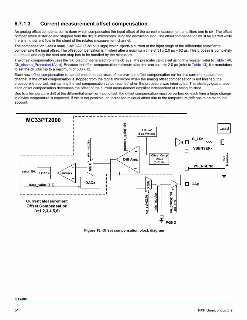
6.7.1.3 Current measurement offset compensation
An analog offset compensation is done which compensates the input offset of the current measurement amplifiers one to six. The offset compensation is started and stopped from the digital microcores using the instruction stoc. The offset compensation must be started while there is no current flow in the shunt of the related measurement channel.
The compensation uses a small 6-bit DAC (5-bit plus sign) which injects a current at the input stage of the differential amplifier to compensate the input offset. The offset compensation is finished after a maximum time of 31 x 2.0 μs = 62 μs. This process is completely automatic and only the start and stop has to be handled by the microcore.
The offset compensation uses the “ck_ofscmp” generated from the ck_sys. The prescaler can be set using this register (refer to Table 146, Ck_ofscmp_Prescaler(1A4h)). Because the offset compensation minimum step time can be up to 2.0 μs (refer to Table 13), it is mandatory to set the ck_ofscmp to a maximum of 500 kHz.
Each new offset compensation is started based on the result of the previous offset compensation run for this current measurement channel. If the offset compensation is stopped from the digital microcore when the analog offset compensation is not finished, the procedure is aborted, maintaining the last compensation value reached when the procedure was interrupted. This strategy guarantees each offset compensation decreases the offset of the current measurement amplifier independent of it being finished.
Due to a temperature drift of the differential amplifier input offset, the offset compensation must be performed each time a huge change in device temperature is expected. If this is not possible, an increased residual offset due to the temperature drift has to be taken into account.
Figure 18. Offset compensation block diagram
Comp x
MC33PT2000
Current Measurement Offset Compensation
(x:1,2,3,4,5,6)
curx_fbk
dacx_value (7:0)
adc_
mod
ex
opam
px_g
ain(
1:0)
G_LSz
VSENSEPx
VSENSENx
Load
oa_e
nyoa
_gai
ny(1
:0)
adc_
mod
ex
oa_s
ely(
2:0)
DACx
Filter x
MU
X
250 mVBias Voltage
Offset CompDACx
(5+1bits)
OAy
PGND
Diff Amp
MU
X
Rse
nsex
51 NXP Semiconductors
PT2000
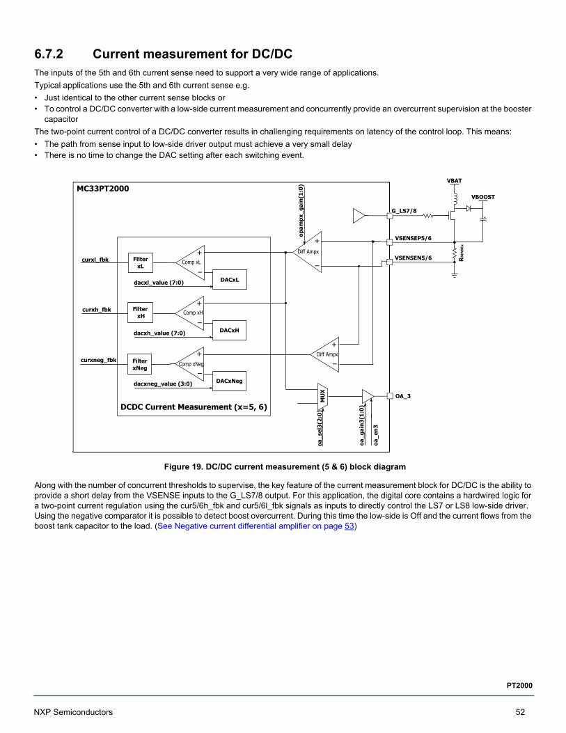
6.7.2 Current measurement for DC/DC The inputs of the 5th and 6th current sense need to support a very wide range of applications.
Typical applications use the 5th and 6th current sense e.g.
• Just identical to the other current sense blocks or • To control a DC/DC converter with a low-side current measurement and concurrently provide an overcurrent supervision at the booster
capacitor
The two-point current control of a DC/DC converter results in challenging requirements on latency of the control loop. This means:
• The path from sense input to low-side driver output must achieve a very small delay• There is no time to change the DAC setting after each switching event.
Figure 19. DC/DC current measurement (5 & 6) block diagram
Along with the number of concurrent thresholds to supervise, the key feature of the current measurement block for DC/DC is the ability to provide a short delay from the VSENSE inputs to the G_LS7/8 output. For this application, the digital core contains a hardwired logic for a two-point current regulation using the cur5/6h_fbk and cur5/6l_fbk signals as inputs to directly control the LS7 or LS8 low-side driver. Using the negative comparator it is possible to detect boost overcurrent. During this time the low-side is Off and the current flows from the boost tank capacitor to the load. (See Negative current differential amplifier on page 53)
G_LS7/8
oa_s
el3(
2:0)
G
OA_3
dacxl_value (7:0)
+
–
VSENSEP5/6
VSENSEN5/6+
–DACxL
curxl_fbk
opam
px_g
ain(
1:0)
oa_g
ain3
(1:0
)
oa_e
n3
RSE
NSE
x
dacxh_value (7:0)
+
–DACxH
curxh_fbk
dacxneg_value (3:0)
+
–DACxNeg
curxneg_fbk
+
–
DCDC Current Measurement (x=5, 6)
Diff Ampx
Diff Ampx
Comp xL
Comp xH
Comp xNeg
MU
X
Filter xL
Filter xH
Filter xNeg
MC33PT2000
+
VBAT
VBOOST
NXP Semiconductors 52
PT2000
6.7.2.1 Negative current differential amplifier
The key characteristic of the second differential amplifier is it works at negative differential input voltages and therefore has a negative gain. This is used to detect overcurrent when the low-side is Off.
The current threshold can be calculated using the following formula.
DAC_VALUE is selected and changed at runtime by the digital microcore by means of the signal dacx_value (3:0).
VDAC LSB is the DAC resolution = 156.25 mV.
VDA_BIAS is the fixed voltage biasing applied to the differential amplifier output = 250 mV.
The Gain Value GDA_DIFF is fixed to -2.0.
RSENSEX is the external sense resistor of the current measurement channel x.
6.7.2.2 Current measurement offset compensation
The analog offset compensation for the differential amplifier 5 and 6 of channel 5 and 6 is done in the same way for channel 1 to 4. The DAC5/6L and the signal Cur5/6l_fbk are used for the offset compensation. Since the accuracy is not actually critical to detect the overcurrent, the differential amplifier 5 and 6 negative do not have offset compensation (see Figure 19).
6.8 OA_x output pins, multiplexer and T & H
6.8.1 General featuresThe output signals of the six current sensing amplifiers are available via three external pins OA_1, OA_2, and OA_3 of the device (refer to Figure 20). With the OAGainx (1:0) and OAxG1 signal, it is possible to select between five different output gains. This feature is used to adapt the device to an ADC input range of 3.3 V or 5.0 V, and also to add the possibility of amplifying the output signal even higher for some special measurement functions. The maximum output voltage at the OA_x pins of VCC5 always has to be taken into account.
For the two higher gains of 3.0 and 5.33, the bias voltage of nominal 250 mV of the input signal is removed before amplifying the signal and adding again to the amplified signal afterwards.
The OA1/2/3 output pins includes the possibility of switching to hi-impedance mode to enable the direct connection of two of these output pins to one micro-controller ADC input. All OA_x output multiplexers can also be switched to VCC2P5 as a third option. This is used to check the connection between the PT2000 and the microcontroller ADC on the ECU level.
Table 31. Boost overcurrent sense amplifier overall gain
Gain value Normal differential mode input voltage Full scale range current with 10 mΩ shunt DAC resolution with 10 mΩ shunt
-2.0 -1047 mV …0 -104.7 A -7.81 A
Table 32. OA_x amplifier gain selection and output voltage
Oagainx(1:0) OAxG1 Gain value Output voltage
d.c. 1 1.0 VIN * Gain
00 0 1.33 VIN * Gain
01 0 2.0 VIN * Gain
10 0 3.0 (VIN – 250 mV) * Gain +250 mV
11 0 5.33 (VIN – 250 mV) * Gain +250 mV
IDACVALUE VDACLSB×( ) 250mV–( )
GDADIFF RSENSE⋅------------------------------------------------------------------------------------------------------------=
53 NXP Semiconductors
PT2000
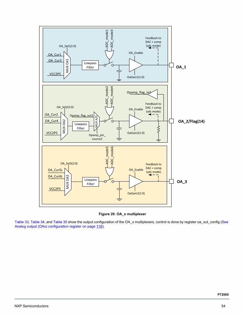
Figure 20. OA_x multiplexer
Table 33, Table 34, and Table 35 show the output configuration of the OA_x multiplexers, control is done by register oa_out_config (See Analog output (OAx) configuration register on page 116).
LowpassFilter
OA_Cur3
OA_Cur1
VCC2P5OaGain1(1:0)
ADC_
mod
e3AD
C_m
ode1
OA_Enable
Feedback toDAC + comp(adc mode)
OA_1
LowpassFilter
OA_Cur4
OA_Cur2
VCC2P5 OaGain2(1:0)
ADC_
mod
e4AD
C_m
ode2
OA_Enable
Feedback toDAC + comp(adc mode)
OA_2/Flag(14)
MUX
OA1
MU
X A/
D
Opamp_pin_source2
Opamp_flag_out2
Opamp_flag_in2
MUX
OA2
LowpassFilter
OaGain2(1:0)
OA_Enable
Feedback toDAC + comp(adc mode)
OA_3
ADC_
mod
e6AD
C_m
ode5
OA_Cur6L
OA_Cur5L
VCC2P5 MU
X O
A3
OA_Sel1(2:0)
OA_Sel2(2:0)
OA_Sel3(2:0)
NXP Semiconductors 54
PT2000
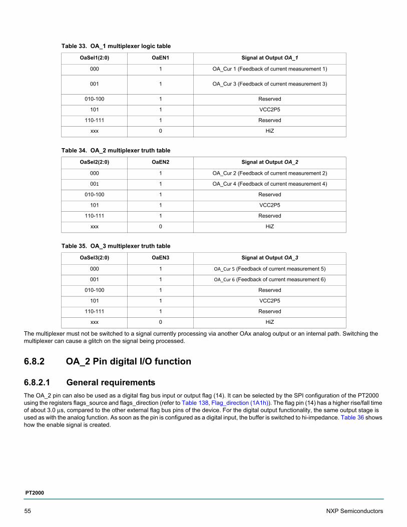
The multiplexer must not be switched to a signal currently processing via another OAx analog output or an internal path. Switching the multiplexer can cause a glitch on the signal being processed.
6.8.2 OA_2 Pin digital I/O function
6.8.2.1 General requirements
The OA_2 pin can also be used as a digital flag bus input or output flag (14). It can be selected by the SPI configuration of the PT2000 using the registers flags_source and flags_direction (refer to Table 138, Flag_direction (1A1h)). The flag pin (14) has a higher rise/fall time of about 3.0 μs, compared to the other external flag bus pins of the device. For the digital output functionality, the same output stage is used as with the analog function. As soon as the pin is configured as a digital input, the buffer is switched to hi-impedance. Table 36 shows how the enable signal is created.
Table 33. OA_1 multiplexer logic table
OaSel1(2:0) OaEN1 Signal at Output OA_1
000 1 OA_Cur 1 (Feedback of current measurement 1)
001 1 OA_Cur 3 (Feedback of current measurement 3)
010-100 1 Reserved
101 1 VCC2P5
110-111 1 Reserved
xxx 0 HiZ
Table 34. OA_2 multiplexer truth table
OaSel2(2:0) OaEN2 Signal at Output OA_2
000 1 OA_Cur 2 (Feedback of current measurement 2)
001 1 OA_Cur 4 (Feedback of current measurement 4)
010-100 1 Reserved
101 1 VCC2P5
110-111 1 Reserved
xxx 0 HiZ
Table 35. OA_3 multiplexer truth table
OaSel3(2:0) OaEN3 Signal at Output OA_3
000 1 OA_Cur 5 (Feedback of current measurement 5)
001 1 OA_Cur 6 (Feedback of current measurement 6)
010-100 1 Reserved
101 1 VCC2P5
110-111 1 Reserved
xxx 0 HiZ
55 NXP Semiconductors
PT2000
6.8.2.2 OA_2 pin I/O voltage
The I/O voltage of the OA_2 pins is not automatically set according to the VCCIO voltage supplied to the device. The OA_2 output amplifier which is also used for the digital output function is supplied by VCC5. The digital input signal to the OA_2 output amplifier is a VCC2P5 based signal. The I/O voltage has to be selected by choosing the right gain of the OA_2 output amplifier. Table 37 shows how to select the proper I/O voltage.
There is a weak pull-down resistor at the OA_2 input/output. This resister is always present, regardless if the digital or analog functionality is selected.
6.8.3 OAx output offset and offset errorIt is important to have a close look at the output offset of the OAx pins and the output voltage values corresponding to load current values. The current measurement amplifiers output signal has a fixed offset of 250 mV and also some variable offset of -28.6 mV to +36.4 mV for this path after analog offset compensation. This offset is independent of the current measurement amplifiers gain setting, but is amplified by the OAx amplifier gain. The OAx amplifier also adds some input offset of ±10…13.5 mV to this calculation. So in sum there is a fixed offset of 250 mV and a variable offset at the input of the OAx amplifier.
For the two higher gains of 3.0 and 5.33, the bias voltage of nominal 250 mV of the input signal is removed before amplifying the signal and added again to the amplified signal afterwards. Table 38 gives some examples for load currents, gain settings, and corresponding output voltage ranges. Note that this calculation only takes into account the offset errors. There are also other errors which have to be considered in a full error calculation.
Table 36. OA2 enable truth table
flags_source flags_directionopamp_pin_source
(2) (reset=0)OaEN2
(reset=0)OA2 Buffer
stateDescription
0 d.c. 0 0 HiZ OA2 pin is used as analog output, enable signal is low
0 d.c. 0 1 On OA2 pin is used as analog output, enable signal is high
1 1 1 - HiZ OA2 pin is used as digital input
1 0 1 - On OA2 pin is used as digital output
Table 37. OA_2 amplifier gain selection (I/O voltage)
OaGain2(1:0) Gain value Used for
00 (reset value) 1.33 3.3 V I/O
01 2.0 5.0 V I/O
10 3.0
11 5.33
Table 38. OAx input and output values
Load current at 10 mΩ shunt/A
Current measurement amplifier gain setting
OAx amplifier gain setting
OAx output voltage Min./mV
OAx output voltage Typ./mV
OAx output voltage Max./mV
0 8.68 1.33 276 333 399
25.8 8.68 1.33 3256 3312 3378
0 19.25 5.33 45 250 497
1 19.25 5.33 1071 1276 1523
2.5 19.25 5.33 2610 2815 3062
NXP Semiconductors 56
PT2000
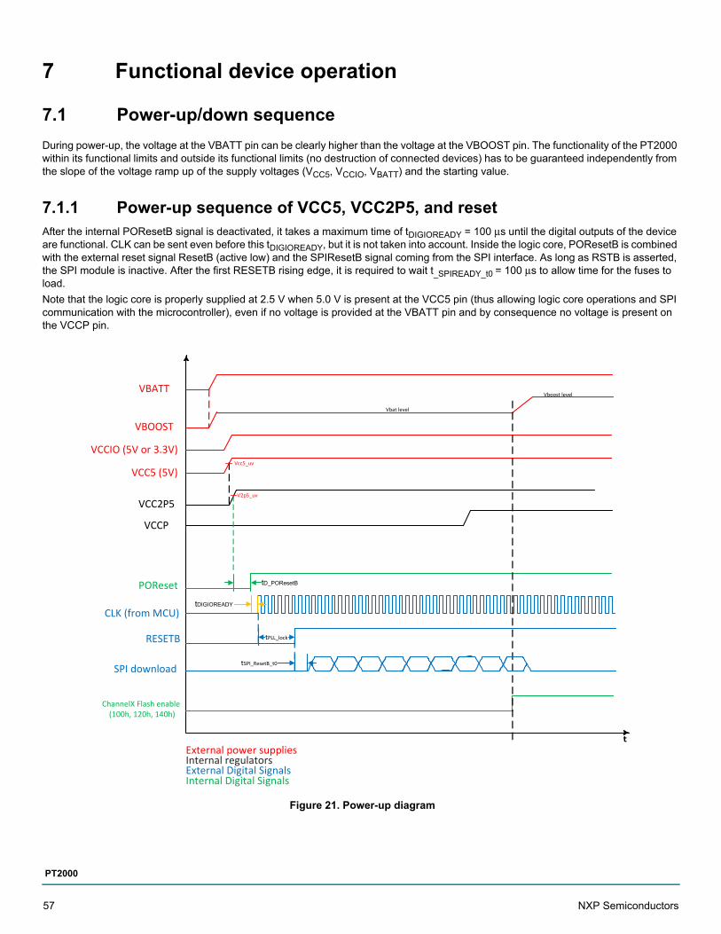
7 Functional device operation
7.1 Power-up/down sequence
During power-up, the voltage at the VBATT pin can be clearly higher than the voltage at the VBOOST pin. The functionality of the PT2000 within its functional limits and outside its functional limits (no destruction of connected devices) has to be guaranteed independently from the slope of the voltage ramp up of the supply voltages (VCC5, VCCIO, VBATT) and the starting value.
7.1.1 Power-up sequence of VCC5, VCC2P5, and resetAfter the internal POResetB signal is deactivated, it takes a maximum time of tDIGIOREADY = 100 μs until the digital outputs of the device are functional. CLK can be sent even before this tDIGIOREADY, but it is not taken into account. Inside the logic core, POResetB is combined with the external reset signal ResetB (active low) and the SPIResetB signal coming from the SPI interface. As long as RSTB is asserted, the SPI module is inactive. After the first RESETB rising edge, it is required to wait t_SPIREADY_t0 = 100 μs to allow time for the fuses to load.
Note that the logic core is properly supplied at 2.5 V when 5.0 V is present at the VCC5 pin (thus allowing logic core operations and SPI communication with the microcontroller), even if no voltage is provided at the VBATT pin and by consequence no voltage is present on the VCCP pin.
Figure 21. Power-up diagram
VBATT
VCCIO (5V or 3.3V)
VCC5 (5V)
VBOOST
VCC2P5
POReset
VCCP
CLK (from MCU)
RESETB
SPI download
ChannelX Flash enable(100h, 120h, 140h)
tD_POResetB
tPLL_lock
Vcc5_uv
V2p5_uv
External power supplies
External Digital SignalsInternal regulators
Internal Digital Signals
Vbat level
Vboost level
tSPI_ResetB_t0
tDIGIOREADY
57 NXP Semiconductors
PT2000
7.1.2 Power-up sequence VCCP and bootstrap capacitors
7.1.2.1 Bootstrap switch control
During initialization phase, the control of the boostrap switch needs to be carefully controlled. The following device configurations are affected.
• Hsx_bs_lowcurrent: the low-current limit (280 μA), which is set only during init independently for each HS pre-driver;• Vsrc_threshold: the VSRC thresholds of each HSx, which during init is set first to 0.5 V and after some time to 1.0 V. After init phase is
finished the VSRC threshold returns to the value defined in the appropriate register (refer to Table 94, Vsrc_threshold_hs_Part2 (16Eh)).• Ls_bias: all ls_bias are set active for all LSx outputs during init phase of any HS pre-driver, and then go back to the configuration defined
in the appropriate register (refer to register Table 126, Ls_bias_config (18Ch)) when all HS pre-drivers are out of the init phase.• Hs_bias: the hs_bias is set inactive for the HSx outputs during init and then returns to the configuration defined in the appropriate
register (refer to Table 125, Hs_bias_config (18Bh)).
During the init phase of the bootstrap capacitors, the vccp_external_enable signal is affected according to what is defined in Table 150, VCCP external enable setting. In particular, as long as at least one HS pre-driver is in bootstrap init mode, the vccp_external_enable setting is set to '0' (internal regulator active), if the value of the DBG pin sampled at reset (POResetB and ResetB) was '1'.
The charging of the bootstrap capacitors starts after reset is deactivated and as soon as the VCCP voltage is ramped up. As soon as the VCCP voltage is above the VCCP undervoltage threshold, a global timer for all hs pre-drivers running on cksys with an end of count value of 36 ms is started. As soon as the timer reaches the end of count value, the Vsrc_threshold is changed from 0.5 V to 1.0 V for all drivers still in init mode. At the same moment, the hsx_src_1V bit is set to '1' for all these drivers.
The bootstrap init for each HS pre-driver ends if one of the following conditions is met:
• The bs ready comparator shows the B_HSx voltage is close to the VCCP voltage and at the same time the S_HSx voltage is below 0.5 V or 1.0 V,
• The clamp is activated and at the same time the S_HSx voltage is below 0.5 V or 1.0 V;• An LS pre-driver connected to the same HS pre-driver is switched on and the corresponding hsx_lsx_act signal is set to '1';• The connection between LS pre-drivers and HS pre-driver is disabled (hsx_ls_act_dis signal = '1'); or• The same HS pre-driver is switched on.
In applications where two HS pre-drivers are connected to the same node by their S_HSx pin directly or via a diode, care must be taken. It is not allowed in these configurations to turn on the hs_bias via the SPI register or the microcode command before all HS pre-drivers finished their bootstrap init. Otherwise an active hs_bias from one pre-driver may block the init of the other. The init mode of each HS pre-driver can be quit by setting the corresponding “hsx_ls_act_dis” bit to '1' (refer to Table 127, Bootstrap_charged (18Dh)). This should be done for each HS pre-driver not used in an application.
7.1.2.2 Using D_LSx pull-down sources to charge bootstrap capacitors
After reset release and after the VCCP voltage is above the UV_VCCP threshold, the charging of the HS pre-driver's bootstrap capacitors via the D_LSx pull-down sources starts automatically, as long as there is a current path from S_HSx of the HS pre-driver to at least one D_LSx pin or to GND. To make this possible, there is a requirement to switch the current limitation of the bootstrap path from about 95 mA to min. 280 μA.
Table 39 shows how long it takes to charge a bootstrap capacitor to 7.0 V using the D_LSx current sources and a bootstrap path current limitation of 280 μA, plus the charge pump current of 20 μA.
Table 39. Charge times bootstrap Cs using D_LSx sources
Bootstrap capacitor size (typ.) Charge time (typ.)/ms
100 nF 2.3
330 nF 7.7
1.0 µF 23.3
2.2 µF 51.3
NXP Semiconductors 58
PT2000
7.1.2.3 Using the charge pump to charge bootstrap capacitors
If there is no current path from S_HSx pin to D_LSx or GND, only the internal CP can be used to charge the bootstrap capacitors during init with a guaranteed current of 20 μA per HS pre-driver. This current is only available if there is no leakage current from B_HSx pin. Any possible leakage current has to be subtracted from this available charge current.
It is not necessary to turn on either the LS MOSFETs or the D_LSx pull-down current sources to charge the bootstrap capacitors during the init phase, if there is at minimum the current loop via the body diode of the external high-side MOSFET present. In addition, there is some leakage current path from S_HSx to PGND. The charge pump starts charging the bootstrap capacitors as soon as the device is supplied with VCC5 and a voltage greater 4.7 V at the VBOOST pin and POResetB is deactivated. Table 40 shows how long it takes to charge a bootstrap capacitor to 7.0 V using the charge pump current of 20 μA.
7.1.2.4 Using LS MOSFETs to charge bootstrap capacitors
After reset release of the device, the charging of the bootstrap capacitors via the D_LSx pull-downs and the internal charge pump starts automatically. If there is the requirement to speed up the initial charging of the bootstrap capacitors, it is possible to switch on an LS MOSFET connected to the HS MOSFET. If the device is configured in a proper way (refer Table 131, Hsx_ls_act (18Fh - 195h)) the bootstrap switch current limit changes to the high limit of about 95 mA as soon as the LS pre-driver is turned on. Because the bootstrap init mode is left for this HS pre-driver, it must be guaranteed that the internal VCCP regulator is already switched on via the SPI bit, if required.
After switching on the internal VCCP regulator, the output buffer capacitor at the VCCP pin is charged. The device is still in a VCCP undervoltage condition, no external MOSFET (HS or LS) can be switched on, and the bootstrap diodes are also kept in the Off state. During ramp up the voltage on the VCCP pin crosses the VCCP undervoltage threshold. After the voltage is above this threshold (plus a minimum 16 μs delay), it is possible to switch on the LS MOSFETs.
There are two possible solutions to charge the HS pre-driver bootstrap capacitors using the path via the LS MOSFETs:
1. Wait for some specific time after VCCP regulator is activated to ensure the VCCP output voltage has reached it's nominal value of
about 7.0 V. This is only possible if the VBATT voltage is at a nominal value. Switch on the LS MOSFET(s) to charge the bootstrap
capacitors. If the VCCP voltage was high enough and the bootstrap capacitors are small compared to the VCCP output buffer
capacitor, this leads to a transfer of charge without crossing the VCCP_UV threshold again. Figure 22 shows this strategy.
Table 40. Charge times bootstrap Cs using CP
Bootstrap capacitor size (typ.) Charge time (typ.)/ms
100 nF 35
330 nF 116
1.0 μF 350
2.2 μF 770
59 NXP Semiconductors
PT2000
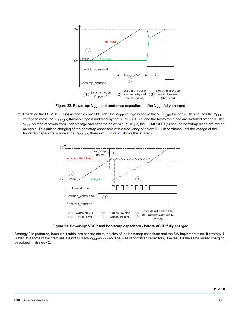
Figure 22. Power-up: VCCP and bootstrap capacitors - after VCCP fully charged
2. Switch on the LS MOSFET(s) as soon as possible after the VCCP voltage is above the VCCP_UV threshold. This causes the VCCP
voltage to cross the VCCP_UV threshold again and thereby the LS MOSFET(s) and the bootstrap diode are switched off again. The
VCCP voltage recovers from undervoltage and after the delay min. of 16 μs, the LS MOSFET(s) and the bootstrap diode are switch
on again. This pulsed charging of the bootstrap capacitors with a frequency of below 50 kHz continues until the voltage of the bootstrap capacitors is above the VCCP_UV threshold. Figure 23 shows this strategy.
Figure 23. Power-up: VCCP and bootstrap capacitors - before VCCP fully charged
Strategy 2 is preferred, because it adds less constraints to the size of the bootstrap capacitors and the SW implementation. If strategy 1 is tried, but some of the premises are not fulfilled (VBATT/VCCP voltage, size of bootstrap capacitors), the result is the same pulsed charging described in strategy 2.
0V
7V
Lowside_command
uv_vccp
Tcharge_VCCP
Boostrap_charged
VCB_HSxVCCP
1
23
1 Switch on VCCP (Vccp_en=1) 2
Wait until VCCP is charged (depend
on CVccp value)3
Switch on low side with microcore
(sto lsx on)
Lowside_on
uv_vccpdelay
VCB_HSxVCCP
uv_vccp_threshold
0V
7V
Boostrap_charged
1 Switch on VCCP (Vccp_en=1) 2 Turn on low side
with microcore 3Low side will switch ON/OFF automatically due to
uv_vccp
1
Lowside_command 2
3
NXP Semiconductors 60
PT2000
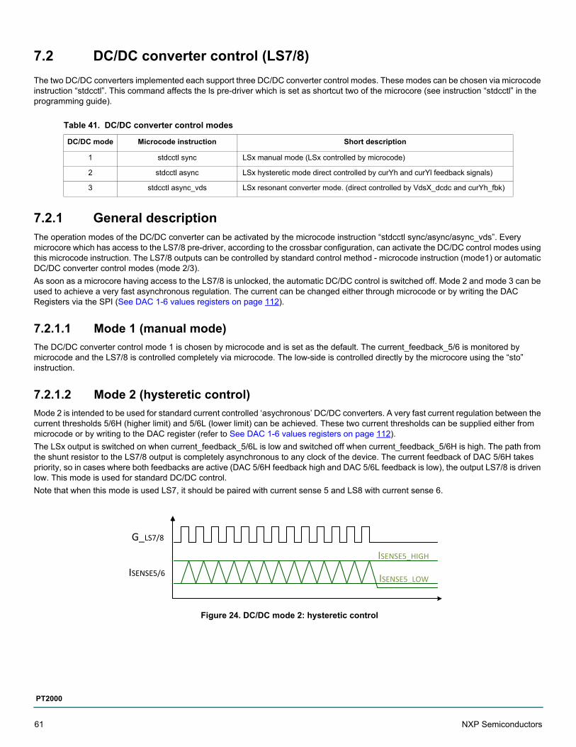
7.2 DC/DC converter control (LS7/8)
The two DC/DC converters implemented each support three DC/DC converter control modes. These modes can be chosen via microcode instruction “stdcctl”. This command affects the ls pre-driver which is set as shortcut two of the microcore (see instruction “stdcctl” in the programming guide).
7.2.1 General descriptionThe operation modes of the DC/DC converter can be activated by the microcode instruction “stdcctl sync/async/async_vds”. Every microcore which has access to the LS7/8 pre-driver, according to the crossbar configuration, can activate the DC/DC control modes using this microcode instruction. The LS7/8 outputs can be controlled by standard control method - microcode instruction (mode1) or automatic DC/DC converter control modes (mode 2/3).
As soon as a microcore having access to the LS7/8 is unlocked, the automatic DC/DC control is switched off. Mode 2 and mode 3 can be used to achieve a very fast asynchronous regulation. The current can be changed either through microcode or by writing the DAC Registers via the SPI (See DAC 1-6 values registers on page 112).
7.2.1.1 Mode 1 (manual mode)
The DC/DC converter control mode 1 is chosen by microcode and is set as the default. The current_feedback_5/6 is monitored by microcode and the LS7/8 is controlled completely via microcode. The low-side is controlled directly by the microcore using the “sto” instruction.
7.2.1.2 Mode 2 (hysteretic control)
Mode 2 is intended to be used for standard current controlled ‘asychronous’ DC/DC converters. A very fast current regulation between the current thresholds 5/6H (higher limit) and 5/6L (lower limit) can be achieved. These two current thresholds can be supplied either from microcode or by writing to the DAC register (refer to See DAC 1-6 values registers on page 112).
The LSx output is switched on when current_feedback_5/6L is low and switched off when current_feedback_5/6H is high. The path from the shunt resistor to the LS7/8 output is completely asynchronous to any clock of the device. The current feedback of DAC 5/6H takes priority, so in cases where both feedbacks are active (DAC 5/6H feedback high and DAC 5/6L feedback is low), the output LS7/8 is driven low. This mode is used for standard DC/DC control.
Note that when this mode is used LS7, it should be paired with current sense 5 and LS8 with current sense 6.
Figure 24. DC/DC mode 2: hysteretic control
Table 41. DC/DC converter control modes
DC/DC mode Microcode instruction Short description
1 stdcctl sync LSx manual mode (LSx controlled by microcode)
2 stdcctl async LSx hysteretic mode direct controlled by curYh and curYl feedback signals)
3 stdcctl async_vds LSx resonant converter mode. (direct controlled by VdsX_dcdc and curYh_fbk)
G_LS7/8
ISENSE5/6
ISENSE5_HIGH
ISENSE5_LOW
61 NXP Semiconductors
PT2000
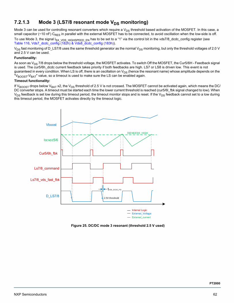
7.2.1.3 Mode 3 (LS7/8 resonant mode VDS monitoring)
Mode 3 can be used for controlling resonant converters which require a VDS threshold based activation of the MOSFET. In this case, a small capacitor (~10 nF) CRES in parallel with the external MOSFET has to be connected, to avoid oscillation when the low-side is off.
To use Mode 3, the signal lSX_VDS_HIGHSPEED_EN has to be set to a “1” via the control bit in the vds7/8_dcdc_config register (see Table 116, Vds7_dcdc_config (182h) & Vds8_dcdc_config (183h)).
VDS fast monitoring of D_LS7/8 uses the same threshold generator as the normal VDS monitoring, but only the threshold voltages of 2.0 V and 2.5 V can be used.
Functionality:
As soon as VDS 7/8 drops below the threshold voltage, the MOSFET activates. To switch Off the MOSFET, the Cur5/6H - Feedback signal is used. The cur5/6h_dcdc current feedback takes priority if both feedbacks are high. LS7 or LS8 is driven low. This event is not guaranteed in every condition. When LS is off, there is an oscillation on VDS (hence the resonant name) whose amplitude depends on the "VBOOST-VBAT" value, so a timeout is used to make sure the LS can be enabled again.
Timeout functionality:
If VBOOST drops below VBAT x2, the VDS threshold of 2.5 V is not crossed. The MOSFET cannot be activated again, which means the DC/DC converter stops. A timeout must be started each time the lower current threshold is reached (cur5/6l_fbk signal changed to low). When VDS feedback is set low during this timeout period, the timeout monitor stops and is reset. If the VDS feedback cannot set to a low during this timeout period, the MOSFET activates directly by the timeout logic.
Figure 25. DC/DC mode 3 resonant (threshold 2.5 V used)
Vboost
Ls7/8_command
D_LS7/8
Ls7/8_vds_fast_fbk
ISENSE5/6
ISENSE5/6_HIGH
Cur5/6h_fbk
2.5V threshold
tVDS_DCDC_PD
Internal LogicExternal_VoltageExternal_current
NXP Semiconductors 62
PT2000
7.3 Device clock manager and PLL init
After 100 μs the clock monitor is enabled, Table 42 shows different strategies to start the device.
The clock manager duty is to detect a low frequency (or missing) input reference or a PLL malfunction. To do so, it monitors the PLL output, to check if the output clock frequency is within acceptable range.This is achieved counting the number of pll_output_clock cycles inside six periods of the backup reference clock (six periods of 1.0 MHz clock = 6.0 μs). The expected number depends on the selected PLL multiplication factor;
• when the factor is 24, it is detected an invalid clock condition when it is possible to count more than 165 or less than 125 pll_output_clock cycles.
• when the factor is 12, it is detected an invalid clock condition when it is possible to count more than 84 or less than 61 pll_output_clock cycles.
After requesting the switch back to the external clock reference the device cannot be accessed via the SPI (see Table 152, backup_clock_status (1A8h)) for about:
• 100 μs if there is a valid external clock available• 290 μs (250 μs+40 μs re-lock time) if there is no valid input clock available and the device has to go back to the backup clock again.
The SPI word transmitted to set the Switch to clock pin bit has to be the last word within a SPI burst.
7.4 SW initialization flow
7.4.1 Power supply, reset, and clock• Supply device
• The device needs 5.0 V supply voltage on the VCC5 pin and 3.3 V or 5.0 V supply voltage on the VCCIO pin• A voltage at the VBATT and/or VBOOST pin is not mandatory for device initialization• As soon as the device is properly supplied at the VCC5 pin, VCC2P5 regulator is started• When VCC2P5 is above a specific threshold, the internal POResetB signal is deactivated• After the internal POResetB signal is deactivated, it takes a maximum time of 100 μs until the digital outputs of the device are
functional• Setup external reference clock of 1.0 MHz at the CLK pin
• The PLL is locked about 25 μs after the external CLK is enabled• If the external clock signal availability cannot be guaranteed within this period, it is recommended to reset the device via ResetB
immediately, or switch to the external clock reference later via the SPI command• Deactivate ResetB signal
• The external reset signal ResetB has to be deactivated if it has been active• As soon as there is no POResetB and ResetB signal active, the internal reset RSTB is deactivated
Table 42. Device clock manager and PLL init
Initial state 1. Step 2. Step 3. Step Result
Device supplied, but in reset (ResetB), no ext. clock
Supply external 1.0 MHz clock at CLK input
Deactivate ResetB —Device accessible after 40 μs (PLL lock
time) and running on ext. clock
Device supplied, but in reset (ResetB), no ext. clock
Supply external 1.0 MHz clock at CLK input
Wait for t > 20 μs Deactivate ResetBDevice accessible immediately and running
on ext. clock
Device supplied, but in reset (ResetB), no ext. clock
Deactivate ResetB — —Device accessible after 140 μs and running
on backup clock
Device supplied, but in reset (ResetB), no ext. clock
Deactivate ResetBSupply external
1.0 MHz clock at CLK input at t < 100 μs
—Device accessible 40 μs (PLL lock time)
after CLK available and running on ext. clock
Device running on backup clock, no ext. clock
Supply external 1.0 MHz clock at CLK input
Request switch to external clock
—Device accessible 100 μs after switch
request and running on ext. clock
Device running on backup clock, no ext. clock
Request switch to external clock
— —Device accessible 290 μs after switch request and running on backup clock
63 NXP Semiconductors
PT2000
7.4.2 SPI configurationThe whole SPI configuration can be done while the device is using the internal backup clock reference. The device registers are not locked after device reset.
• Check if device is accessible via the SPI• Check if the device is accessible via the SPI by reading the ID/REV register
• Init the main configuration registers• Init the main configuration registers including the Clock Prescaler, Flag pin setup,…• If the application uses the internal VCCP regulator to supply the pre-drivers, this regulator must be switched on now
• Set code width• If the microcode transmits using one single SPI burst, it is mandatory to write the code width register of each channel used• If the microcode is transmitted using multiple bursts which include information about the number of words, the code width register
can also be written• The code width must be set before setting the pre_flash_enable bit, because the checksum calculation information is required
• Download microcode• Download microcode via the SPI for each channel used
• Set the CRC32 checksum• Set the checksum_l/h register (32-bit) of each channel used
• Init diagnostics configuration registers• Init I/O configuration registers• Init channel configuration registers• Init DRAM values for the first time
• Depending on the application and the microcode, it could be required to set up DRAM parameters of the channels used• Set the lock bit in the device_lock register (optional)
7.4.3 Clock monitor, flash enable, and DrvEn• Check if the device is running on an external reference clock
• It is recommended to verify the device is running on the external clock reference. This can be checked by reading a bit in the driver_status SPI register
• If the device is running on the backup clk, it is possible to switch the clock manager to external reference via a SPI command• This is only mandatory if the external clock reference is not available in time and the device is running on the backup oscillator’s clock• The clock manager is forced to try to switch back to the external reference by a SPI write to a dedicated bit• SPI transfers have to be avoided when switching the clock reference. The SPI module is in reset as long as there is no valid clock• Do not switch the clock reference while the first checksum calculation is running
• Set the pre_flash_enable bit• Set the pre_flash_enable bit of the used channel(s)• This bit “freezes” the CRAM and enables the signature unit to perform the CRC32 check for the first time• After the signature unit has finished the first CRC32 check successfully, it sets the flash_enable bit to start the microcore(s) of the
used channel(s)• The microcode should check for the flash_enable bit with a timeout ensuring the microcores are running
• Activate the DrvEn signal• Depending on the application and the microcode, it could be required to activate the DrvEn signal if deactivated
7.5 BIST
The device has a built-in self test (BIST) for the memory (MBIST for CRAM and DRAM) and for the logic core (LBIST). The BIST can be started by the SPI (see Table 170, Bist_interface in write mode (1BDh)). A full LBIST check of the device digital core and MBIST check of the device memories can be required accessing the BIST_register in Write mode and writing a 16-bit password. This request is accepted only if all three CRAMs are unlocked. It is recommended to run MBIST and LBIST during the initialization phase, since the DRAM and CRAM are erased during BIST.
After this request is performed, the LBIST and MBIST check starts and its evolution can be monitored accessing the same BIST_register in read mode.
NXP Semiconductors 64
PT2000
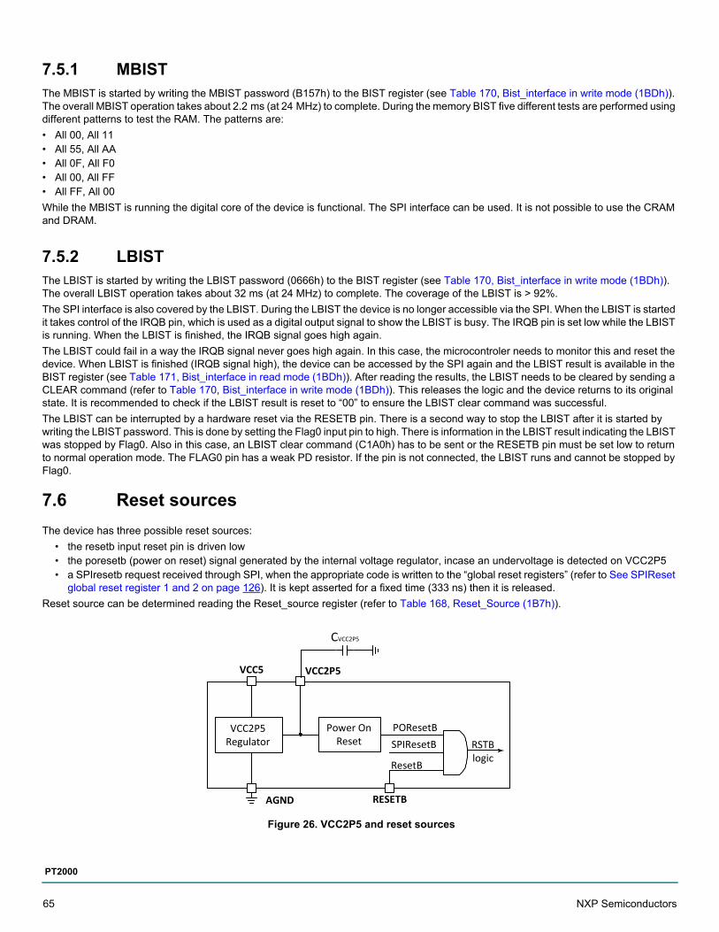
7.5.1 MBISTThe MBIST is started by writing the MBIST password (B157h) to the BIST register (see Table 170, Bist_interface in write mode (1BDh)). The overall MBIST operation takes about 2.2 ms (at 24 MHz) to complete. During the memory BIST five different tests are performed using different patterns to test the RAM. The patterns are:
• All 00, All 11• All 55, All AA• All 0F, All F0• All 00, All FF• All FF, All 00
While the MBIST is running the digital core of the device is functional. The SPI interface can be used. It is not possible to use the CRAM and DRAM.
7.5.2 LBISTThe LBIST is started by writing the LBIST password (0666h) to the BIST register (see Table 170, Bist_interface in write mode (1BDh)). The overall LBIST operation takes about 32 ms (at 24 MHz) to complete. The coverage of the LBIST is > 92%.
The SPI interface is also covered by the LBIST. During the LBIST the device is no longer accessible via the SPI. When the LBIST is started it takes control of the IRQB pin, which is used as a digital output signal to show the LBIST is busy. The IRQB pin is set low while the LBIST is running. When the LBIST is finished, the IRQB signal goes high again.
The LBIST could fail in a way the IRQB signal never goes high again. In this case, the microcontroler needs to monitor this and reset the device. When LBIST is finished (IRQB signal high), the device can be accessed by the SPI again and the LBIST result is available in the BIST register (see Table 171, Bist_interface in read mode (1BDh)). After reading the results, the LBIST needs to be cleared by sending a CLEAR command (refer to Table 170, Bist_interface in write mode (1BDh)). This releases the logic and the device returns to its original state. It is recommended to check if the LBIST result is reset to “00” to ensure the LBIST clear command was successful.
The LBIST can be interrupted by a hardware reset via the RESETB pin. There is a second way to stop the LBIST after it is started by writing the LBIST password. This is done by setting the Flag0 input pin to high. There is information in the LBIST result indicating the LBIST was stopped by Flag0. Also in this case, an LBIST clear command (C1A0h) has to be sent or the RESETB pin must be set low to return to normal operation mode. The FLAG0 pin has a weak PD resistor. If the pin is not connected, the LBIST runs and cannot be stopped by Flag0.
7.6 Reset sources
The device has three possible reset sources:
• the resetb input reset pin is driven low• the poresetb (power on reset) signal generated by the internal voltage regulator, incase an undervoltage is detected on VCC2P5• a SPIresetb request received through SPI, when the appropriate code is written to the “global reset registers” (refer to See SPIReset
global reset register 1 and 2 on page 126). It is kept asserted for a fixed time (333 ns) then it is released.
Reset source can be determined reading the Reset_source register (refer to Table 168, Reset_Source (1B7h)).
Figure 26. VCC2P5 and reset sources
CVCC2P5
POResetBSPIResetB
ResetB
RSTBlogic
RESETBAGND
VCC5 VCC2P5
VCC2P5Regulator
Power OnReset
65 NXP Semiconductors
PT2000
As long as RSTB is asserted, the SPI module is also inactive. In order to understand when the device has gone out of reset state, the microcontroller should poll the device on the SPI. This can be done by either sending any message to the device and checking for the control pattern (A8h) on the MISO during the command word or by reading out any register with a reset value not equal to zero (e.g. ID register).
7.7 Cipher unit
This block has the function to secure the code downloaded by the microcontroller into the code RAM via the SPI. The data loaded at device startup must be encrypted with the suitable cipher. This block receives an encoded SPI stream and decodes it at runtime. The decoded microcode is then stored in the code RAM. This feature cannot be disabled. The cipher algorithm is re-initialized every time the code memory is selected by a write operation to the Selection register (3FFh).
7.8 Ground connections
The device integrates three separate ground pins: PGND, DGND, and AGND:
• PGND is the substrate connection and is only connected to the package exposed pad, to guarantee a low-impedance connection and get optimized EMC performances. PGND is the reference ground for the VCCP regulator, some analog functions, and all of the low-side pre-drivers. It is highly recommended to directly connect PGND to the ECU ground plane.
• DGND is the reference ground for the digital logic core. It is highly recommended to directly connect DGND to the ECU ground plane.The microcontroller as well as other logic devices communicating with the device should share the same reference ground connected to the ground plane to prevent noise.
• AGND is the ground for all the noise sensitive analog blocks integrated into the device. This pin should be connected to the analog ground of the ECU. A star connection is recommended to guarantee a clean analog signal acquisition of the OAX_x pins from the MCU.
Due to their functionality, some analog functions are referred to PGND:
• VDS monitors the low-side drivers• VSRC monitors the high-side drivers• The load biasing S_HSX regulator and the D_LSx pull-down
All the ground pins of the device should be connected to the same ground voltage. Even during transient conditions, the voltage difference between PGND, DGND, and AGND must be limited to ±0.3 V. The layout of the ground connection of the ECU should be carefully designed to limit the ground noise generated as much as possible, for instance during fast switching of the external power MOSFETs.
The decoupling and filter capacitors at the different supply voltage pins should be implemented as described by the following:
• VCC5 to AGND• VCCIO to DGND• VCC2P5 to DGND• VCCP to PGND• VBATT to PGND• VBOOST to AGND or PGND
7.8.1 Detection of missing GND connections The PT2000 can detect any single or multiple missing connection of any ground pin (PGND, DGND, AGND) of the device. At least one ground must remain connected to allow the loss of ground detection. If the ground disconnection is detected, the internal signal uv_vccp is asserted and all the pre-drivers are disabled. The ground lost detection is filtered to allow the device to work in a proper way for a time of typically tFILTER_UVVCCP via the uv_vccp signal.
7.9 Shutoff path via the DrvEn pin
The device includes a shutoff path via the DrvEn pin, which is used to safely disable the solenoid injection power stage in a fault condition of the ECU. When the DrvEn pin is negated, all pre-drivers (w/o configuration option for DrvEn) must be switched off. Status of the DRVEN pin can be read back by the SPI (refer to Table 162).
The shutoff path also works in a defined way (switch off all pre-drivers) when DrvEn is negated, even when the PT2000 is stressed with a voltage of up to 36 V at the supply and/or microcore interface (SPI, Startx,…) pins. Digital interface pins of the PT2000 are self-protected against a voltage of up to 36 V: CLK, IRQB, ResetB, DrvEn, MISO, MOSI, SCLK, CSB, Dbg, Startx (7x), Flagx (4x), OA_x (3x).
NXP Semiconductors 66
PT2000
7.9.1 DrvEn shutoff path of the high-side pre-driverThe DrvEn path for the HS pre-drivers HS1 to HS4 and HS6 is implemented to ensure a high safety level. It is designed with a high level of independence, because there is a direct wire from this pin to the HS pre-driver input and the failure rate of this functionally is very low.
If any of the following failures occur, the shut off path is still functional or the driver must be in a safe off state. These failures are:
• Missing clock signal for the device digital core• Missing supply voltage for the device digital core• Missing supply voltage of level shifter• Missing supply voltage (VBS) of HS pre-driver• Single damaged pre-driver
7.9.2 DrvEn Shutoff path of the low-side pre-driverThe DrvEn path for the LS pre-drivers LS1 to LS5 is implemented to ensure a high safety level. It is designed with a high level of independence, because there is a direct wire from this pin to the HS pre-driver input and the failure rate of this functionally is very low.
If any of the following failures occur, the shut off path is still functional or the driver must be in a safe off state. These failures are:
• Missing clock signal for the device digital core• Missing supply voltage for the device digital core• Missing supply voltage VCCP of LS pre-driver• Single damaged pre-driver
Table 43. DrvEn path for HS pre-drivers
HS pre-driver Implementation
HS1
Direct wire from the DrvEn pin to the HS pre-driver input. High independence and low FIT rate.
HS2
HS3
HS4
HS6
HS5Configuration option for the DrvEn path. The signal is routed via the digital core only.
HS7
Table 44. DrvEn path for LS pre-drivers
LS Pre-driver Implementation
LS1
Direct wire from the DrvEn pin to the LS pre-driver input. High independence and low FIT rate.
LS2
LS3
LS4
LS6
LS5Configuration option for the DrvEn path. The signal is routed via the digital core only.
LS7
67 NXP Semiconductors
PT2000
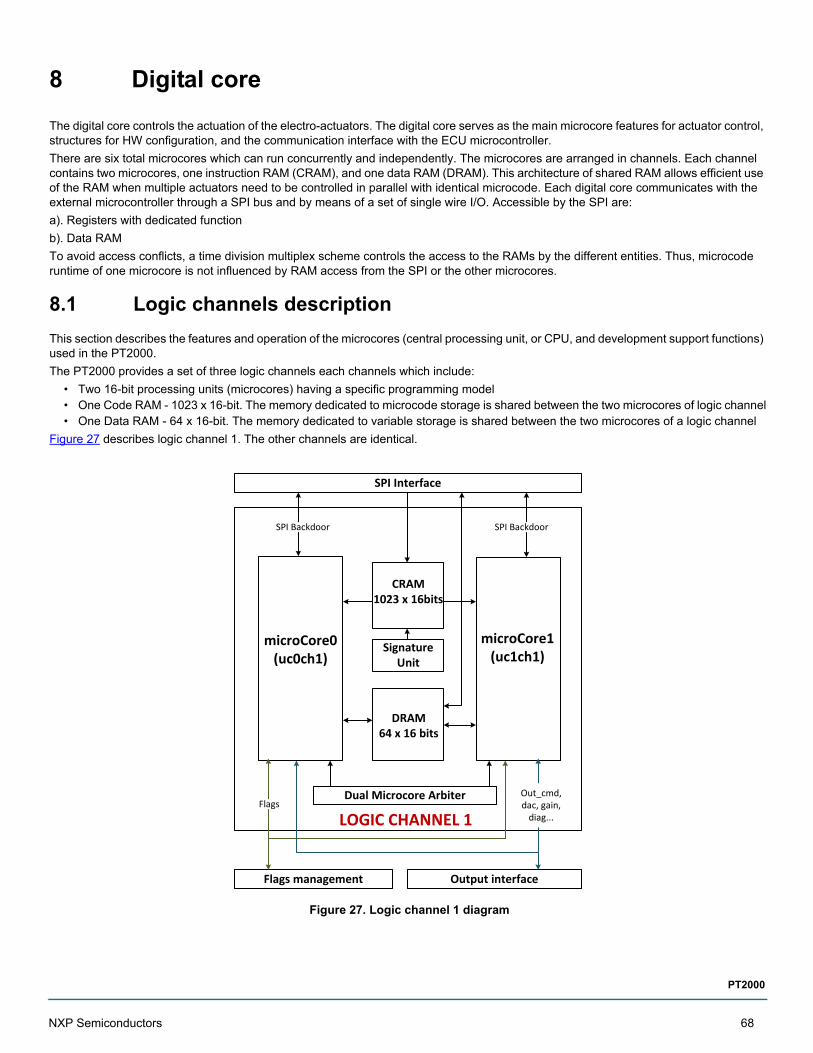
8 Digital core
The digital core controls the actuation of the electro-actuators. The digital core serves as the main microcore features for actuator control, structures for HW configuration, and the communication interface with the ECU microcontroller.
There are six total microcores which can run concurrently and independently. The microcores are arranged in channels. Each channel contains two microcores, one instruction RAM (CRAM), and one data RAM (DRAM). This architecture of shared RAM allows efficient use of the RAM when multiple actuators need to be controlled in parallel with identical microcode. Each digital core communicates with the external microcontroller through a SPI bus and by means of a set of single wire I/O. Accessible by the SPI are:
a). Registers with dedicated function
b). Data RAM
To avoid access conflicts, a time division multiplex scheme controls the access to the RAMs by the different entities. Thus, microcode runtime of one microcore is not influenced by RAM access from the SPI or the other microcores.
8.1 Logic channels description
This section describes the features and operation of the microcores (central processing unit, or CPU, and development support functions) used in the PT2000.
The PT2000 provides a set of three logic channels each channels which include:
• Two 16-bit processing units (microcores) having a specific programming model• One Code RAM - 1023 x 16-bit. The memory dedicated to microcode storage is shared between the two microcores of logic channel• One Data RAM - 64 x 16-bit. The memory dedicated to variable storage is shared between the two microcores of a logic channel
Figure 27 describes logic channel 1. The other channels are identical.
Figure 27. Logic channel 1 diagram
microCore0 (uc0ch1)
CRAM1023 x 16bits
DRAM64 x 16 bits
Signature Unit
SPI Interface
microCore1(uc1ch1)
SPI Backdoor SPI Backdoor
Flags management Output interface
FlagsDual Microcore Arbiter Out_cmd,
dac, gain, diag...LOGIC CHANNEL 1
NXP Semiconductors 68
PT2000
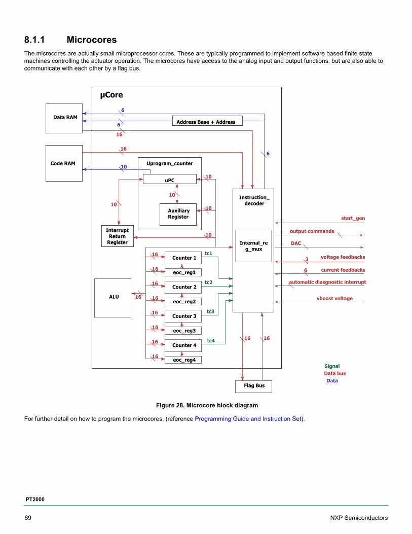
8.1.1 MicrocoresThe microcores are actually small microprocessor cores. These are typically programmed to implement software based finite state machines controlling the actuator operation. The microcores have access to the analog input and output functions, but are also able to communicate with each other by a flag bus.
Figure 28. Microcore block diagram
For further detail on how to program the microcores, (reference Programming Guide and Instruction Set).
Code RAM
Auxiliary Register
Address Base + Address
Instruction_ decoder
Flag Bus
Counter 2
eoc_reg2
Counter 1
eoc_reg1
Counter 3
eoc_reg3
Counter 4
eoc_reg4
ALU
Uprogram_counter
Data RAM
start_gen
output commands
DAC
voltage feedbacks
current feedbacks
automatic diasgnostic interrupt
μCore
10
10
16
10
10
16
6
6
6
16 16
16
16
16
16
16
16
SignalData busData
16
16
16
Interrupt Return
Register
10
10
Internal_reg_mux
tc1
tc2
tc3
tc4
uPC
3
6
vboost voltage
69 NXP Semiconductors
PT2000
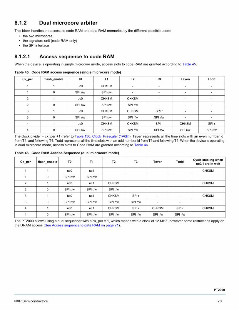
8.1.2 Dual microcore arbiterThis block handles the access to code RAM and data RAM memories by the different possible users:
• the two microcores• the signature unit (code RAM only)• the SPI interface
8.1.2.1 Access sequence to code RAM
When the device is operating in single microcore mode, access slots to code RAM are granted according to Table 45.
The clock divider = ck_per +1 (refer to Table 136, Clock_Prescaler (1A0h)). Teven represents all the time slots with an even number id from T4, and following T4. Todd represents all the time slots with an odd number id from T5 and following T5. When the device is operating in dual microcore mode, access slots to Code RAM are granted according to Table 46.
The PT2000 allows using a dual sequencer with a ck_per = 1, which means with a clock at 12 MHZ, however some restrictions apply on the DRAM access (See Access sequence to data RAM on page 71).
Table 45. Code RAM access sequence (single microcore mode)
Ck_per flash_enable T0 T1 T2 T3 Teven Todd
1 1 uc0 CHKSM - - - -
1 0 SPI r/w SPI r/w - - - -
2 1 uc0 CHKSM CHKSM - - -
2 0 SPI r/w SPI r/w SPI r/w - - -
3 1 uc0 CHKSM CHKSM SPI r - -
3 0 SPI r/w SPI r/w SPI r/w SPI r/w - -
4 1 uc0 CHKSM CHKSM SPI r CHKSM SPI r
4 0 SPI r/w SPI r/w SPI r/w SPI r/w SPI r/w SPI r/w
Table 46. Code RAM Access Sequence (dual microcore mode)
Ck_per flash_enable T0 T1 T2 T3 Teven ToddCycle stealing when
uc0/1 are in wait
1 1 uc0 uc1 CHKSM
1 0 SPI r/w SPI r/w
2 1 uc0 uc1 CHKSM CHKSM
2 0 SPI r/w SPI r/w SPI r/w
3 1 uc0 uc1 CHKSM SPI r - - CHKSM
3 0 SPI r/w SPI r/w SPI r/w SPI r/w - -
4 1 uc0 uc1 CHKSM SPI r CHKSM SPI r CHKSM
4 0 SPI r/w SPI r/w SPI r/w SPI r/w SPI r/w SPI r/w
NXP Semiconductors 70
PT2000
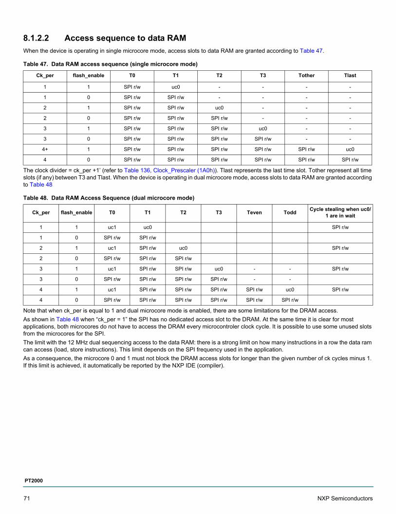
8.1.2.2 Access sequence to data RAM
When the device is operating in single microcore mode, access slots to data RAM are granted according to Table 47.
The clock divider = ck_per +1’ (refer to Table 136, Clock_Prescaler (1A0h)). Tlast represents the last time slot. Tother represent all time slots (if any) between T3 and Tlast. When the device is operating in dual microcore mode, access slots to data RAM are granted according to Table 48
Note that when ck_per is equal to 1 and dual microcore mode is enabled, there are some limitations for the DRAM access.
As shown in Table 48 when “ck_per = 1” the SPI has no dedicated access slot to the DRAM. At the same time it is clear for most applications, both microcores do not have to access the DRAM every microcontroler clock cycle. It is possible to use some unused slots from the microcores for the SPI.
The limit with the 12 MHz dual sequencing access to the data RAM: there is a strong limit on how many instructions in a row the data ram can access (load, store instructions). This limit depends on the SPI frequency used in the application.
As a consequence, the microcore 0 and 1 must not block the DRAM access slots for longer than the given number of ck cycles minus 1. If this limit is achieved, it automatically be reported by the NXP IDE (compiler).
Table 47. Data RAM access sequence (single microcore mode)
Ck_per flash_enable T0 T1 T2 T3 Tother Tlast
1 1 SPI r/w uc0 - - - -
1 0 SPI r/w SPI r/w - - - -
2 1 SPI r/w SPI r/w uc0 - - -
2 0 SPI r/w SPI r/w SPI r/w - - -
3 1 SPI r/w SPI r/w SPI r/w uc0 - -
3 0 SPI r/w SPI r/w SPI r/w SPI r/w - -
4+ 1 SPI r/w SPI r/w SPI r/w SPI r/w SPI r/w uc0
4 0 SPI r/w SPI r/w SPI r/w SPI r/w SPI r/w SPI r/w
Table 48. Data RAM Access Sequence (dual microcore mode)
Ck_per flash_enable T0 T1 T2 T3 Teven ToddCycle stealing when uc0/
1 are in wait
1 1 uc1 uc0 SPI r/w
1 0 SPI r/w SPI r/w
2 1 uc1 SPI r/w uc0 SPI r/w
2 0 SPI r/w SPI r/w SPI r/w
3 1 uc1 SPI r/w SPI r/w uc0 - - SPI r/w
3 0 SPI r/w SPI r/w SPI r/w SPI r/w - -
4 1 uc1 SPI r/w SPI r/w SPI r/w SPI r/w uc0 SPI r/w
4 0 SPI r/w SPI r/w SPI r/w SPI r/w SPI r/w SPI r/w
71 NXP Semiconductors
PT2000
Table 49 shows the smallest period in μs and ck (12 MHz) clock cycles between the address available and first read data bit for SPI read access, which could occur based on a given SPI baud rate.
8.1.3 Signature unitThe task of the signature unit is to compute a checksum of the CRAM to detect possible memory corruption.
The computation is first started when the corresponding CRAM is locked by the pre_flash_enable (see Table 58, Flash_enable (100h, 120h, 140h)). When the computation is complete, the result of the computation is compared to the checksum registers (see Table 66, checksum_h (108h, 128h, 148h)) and Table 67, checksum_l (109h, 129h, 149h)). These registers contain the golden checksum, provided during the init phase through the SPI and calculated automatically by the PT2000 IDE.
If the result is correct, the signature unit sets the flash_enable bit (see Table 58, Flash_enable (100h, 120h, 140h)). If the result is not correct, an interrupt (optional, refer to Table 58, Flash_enable (100h, 120h, 140h)) is issued towards the microcontroller and both microcores accessing the same CRAM are disabled.
The signature unit can be disabled by writing the Checksum_failure_disable bit in the flash_enable_reg (refer to Table 58, Flash_enable (100h, 120h, 140h)). When the signature is disabled, the flash_enable bit is set immediately after the pre_flash_enable bit and a failed checksum causes only a warning (set the appropriate bit in the flash_enable register) without disabling code execution.
The computation requires a different time according to the ck_per value and to the code_width (refer to Table 65, code_width (107h, 127h, 147h)). The worst case computation time for a ck_per of 1 and higher (ck = cksys/2+1 or smaller) is 20 * tCKSYS * (code_width-2). For example, for a completely used memory, a ck_per of 2 and a cksys clock frequency of 24 MHz (ck at 6.0 MHz), the computation takes 851 μs.
The signature unit works only for a code width of 3 or larger. If a shorter code of 1 to 2 words is used, the signature unit has to be disabled.
8.1.4 SPI backdoorIt is also possible to access (both to read and to write) to all the registers normally accessible through the SPI by using an SPI backdoor. Both the SPI read and write operations are multi cycle operations. Table 51 shows the number of cycles needed. The registers must not be changed while the operation is in progress.
To read an SPI register, first the 8 LSBs of the address must be provided in the 8 LSBs of the “SPI address” at internal memory map address. A read operation must then be requested with the “rdspi” instruction (refer to programming guide). The result is available at the “SPI data” address of the internal memory map.
To write an SPI register, first the 8 LSBs of the address must be provided in the 8 LSBs of the “SPI address” address and the data to write must be provided at the “SPI data” address. Then a write operation must be requested with the “wrspi” instruction (refer to programming guide).
There are some access limitations when requesting write access to SPI registers via the SPI backdoor:
• First of all, it is only possible to write to SPI registers which are not locked at the moment the write operation “wrspi” is requested.• For some special registers there are additional limitations dependant on the configuration of the device. Table 51 shows the different
limitations.
Table 49. SPI baud rate and DRAM access sequence for the ck_prescaler = “1”
SPI baud rate (MHz)Minimum SPI read address to first read data bit delay (5 bits)
μs ck Cycles (12 MHz)
1.0 5.0 60
2.0 2.5 30
4.0 1.25 15
8.0 0.625 7.5
10 0.5 6.0
NXP Semiconductors 72
PT2000
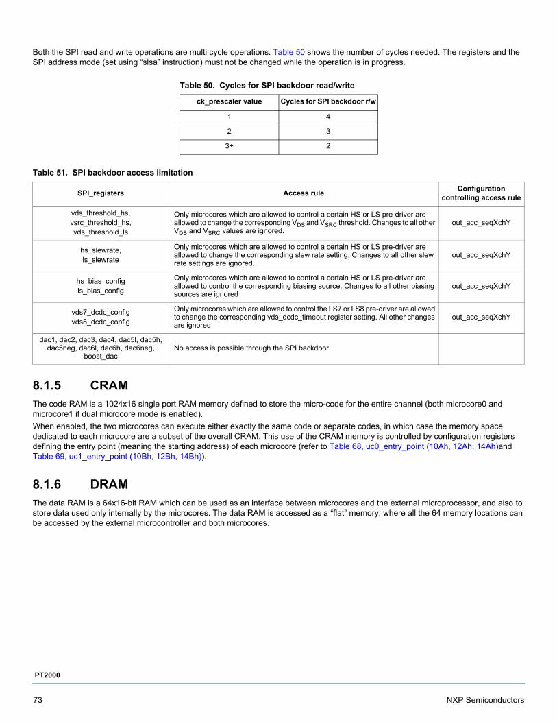
Both the SPI read and write operations are multi cycle operations. Table 50 shows the number of cycles needed. The registers and the SPI address mode (set using “slsa” instruction) must not be changed while the operation is in progress.
8.1.5 CRAMThe code RAM is a 1024x16 single port RAM memory defined to store the micro-code for the entire channel (both microcore0 and microcore1 if dual microcore mode is enabled).
When enabled, the two microcores can execute either exactly the same code or separate codes, in which case the memory space dedicated to each microcore are a subset of the overall CRAM. This use of the CRAM memory is controlled by configuration registers defining the entry point (meaning the starting address) of each microcore (refer to Table 68, uc0_entry_point (10Ah, 12Ah, 14Ah)and Table 69, uc1_entry_point (10Bh, 12Bh, 14Bh)).
8.1.6 DRAMThe data RAM is a 64x16-bit RAM which can be used as an interface between microcores and the external microprocessor, and also to store data used only internally by the microcores. The data RAM is accessed as a “flat” memory, where all the 64 memory locations can be accessed by the external microcontroller and both microcores.
Table 50. Cycles for SPI backdoor read/write
ck_prescaler value Cycles for SPI backdoor r/w
1 4
2 3
3+ 2
Table 51. SPI backdoor access limitation
SPI_registers Access ruleConfiguration
controlling access rule
vds_threshold_hs,vsrc_threshold_hs,vds_threshold_ls
Only microcores which are allowed to control a certain HS or LS pre-driver are allowed to change the corresponding VDS and VSRC threshold. Changes to all other VDS and VSRC values are ignored.
out_acc_seqXchY
hs_slewrate,ls_slewrate
Only microcores which are allowed to control a certain HS or LS pre-driver are allowed to change the corresponding slew rate setting. Changes to all other slew rate settings are ignored.
out_acc_seqXchY
hs_bias_configls_bias_config
Only microcores which are allowed to control a certain HS or LS pre-driver are allowed to control the corresponding biasing source. Changes to all other biasing sources are ignored
out_acc_seqXchY
vds7_dcdc_configvds8_dcdc_config
Only microcores which are allowed to control the LS7 or LS8 pre-driver are allowed to change the corresponding vds_dcdc_timeout register setting. All other changes are ignored
out_acc_seqXchY
dac1, dac2, dac3, dac4, dac5l, dac5h, dac5neg, dac6l, dac6h, dac6neg,
boost_dacNo access is possible through the SPI backdoor
73 NXP Semiconductors
PT2000
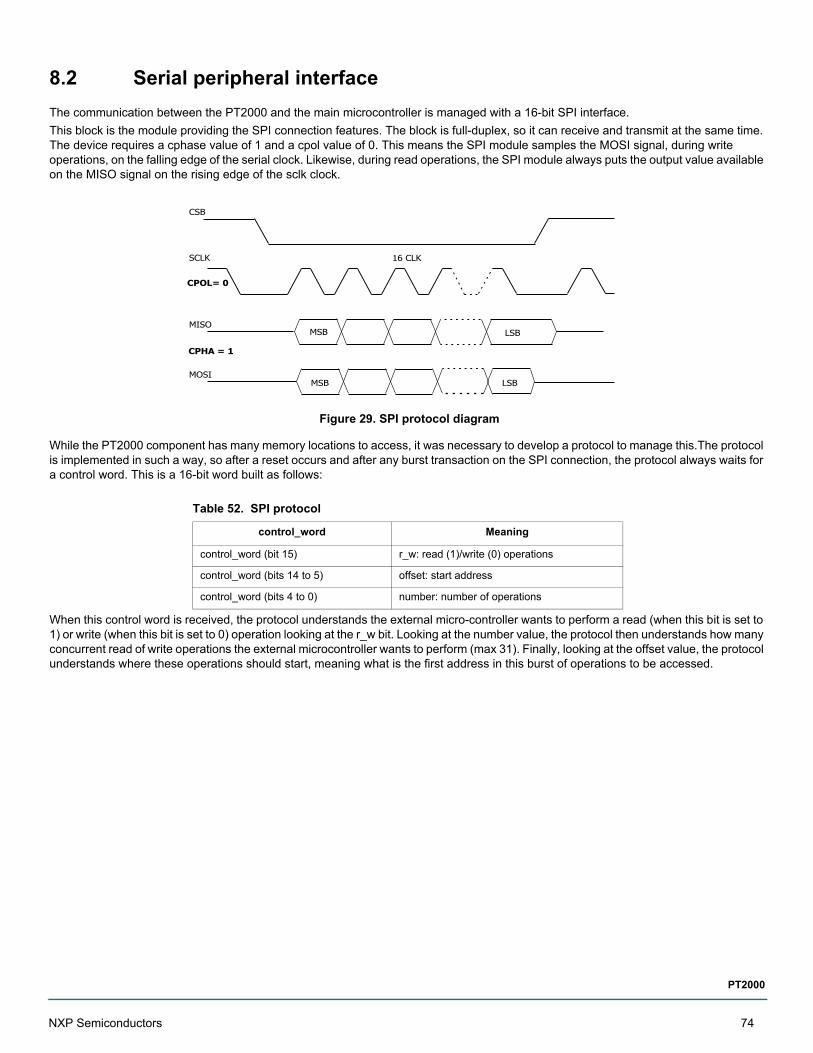
8.2 Serial peripheral interface
The communication between the PT2000 and the main microcontroller is managed with a 16-bit SPI interface.
This block is the module providing the SPI connection features. The block is full-duplex, so it can receive and transmit at the same time. The device requires a cphase value of 1 and a cpol value of 0. This means the SPI module samples the MOSI signal, during write operations, on the falling edge of the serial clock. Likewise, during read operations, the SPI module always puts the output value available on the MISO signal on the rising edge of the sclk clock.
Figure 29. SPI protocol diagram
While the PT2000 component has many memory locations to access, it was necessary to develop a protocol to manage this.The protocol is implemented in such a way, so after a reset occurs and after any burst transaction on the SPI connection, the protocol always waits for a control word. This is a 16-bit word built as follows:
When this control word is received, the protocol understands the external micro-controller wants to perform a read (when this bit is set to 1) or write (when this bit is set to 0) operation looking at the r_w bit. Looking at the number value, the protocol then understands how many concurrent read of write operations the external microcontroller wants to perform (max 31). Finally, looking at the offset value, the protocol understands where these operations should start, meaning what is the first address in this burst of operations to be accessed.
Table 52. SPI protocol
control_word Meaning
control_word (bit 15) r_w: read (1)/write (0) operations
control_word (bits 14 to 5) offset: start address
control_word (bits 4 to 0) number: number of operations
CSB
SCLK
MISO
MOSI
MSB
MSB
LSB
LSB
CPOL= 0
CPHA = 1
16 CLK
NXP Semiconductors 74
PT2000
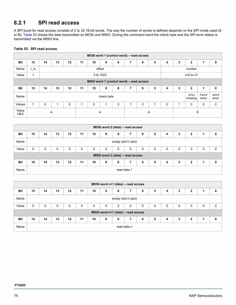
8.2.1 SPI read accessA SPI burst for read access consists of 2 to 32 16-bit words. The way the number of words is defined depends on the SPI mode used (A or B). Table 53 shows the data transmitted on MOSI and MISO. During the command word the check byte and the SPI error status is transmitted via the MISO line.
Table 53. SPI read access
MOSI word 1 (control word) – read access
Bit 15 14 13 12 11 10 9 8 7 6 5 4 3 2 1 0
Name r_w offset number
Value 1 0 to 1023 n=0 to 31
MISO word 1 (control word) – read access
Bit 15 14 13 12 11 10 9 8 7 6 5 4 3 2 1 0
Name check bytecksys
missingframe error
word error
Values 1 0 1 0 1 0 1 0 1 0 1 0 1 0 0 0
Value HEX
A A A 8
MOSI word 2 (data) – read access
Bit 15 14 13 12 11 10 9 8 7 6 5 4 3 2 1 0
Name empty (don’t care)
Value 0 0 0 0 0 0 0 0 0 0 0 0 0 0 0 0
MISO word 2 (data) – read access
Bit 15 14 13 12 11 10 9 8 7 6 5 4 3 2 1 0
Name read data 1
MOSI word n+1 (data) – read access
Bit 15 14 13 12 11 10 9 8 7 6 5 4 3 2 1 0
Name empty (don’t care)
Value 0 0 0 0 0 0 0 0 0 0 0 0 0 0 0 0
MISO word n+1 (data) – read access
Bit 15 14 13 12 11 10 9 8 7 6 5 4 3 2 1 0
Name read data n
75 NXP Semiconductors
PT2000
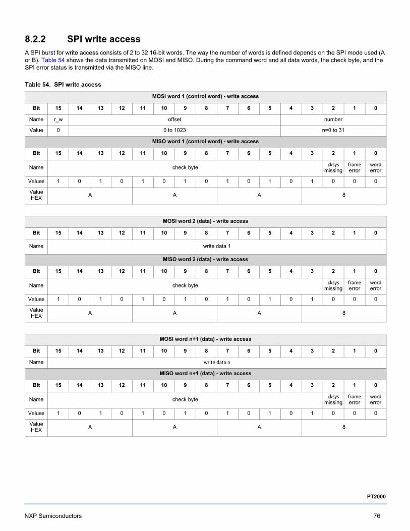
8.2.2 SPI write accessA SPI burst for write access consists of 2 to 32 16-bit words. The way the number of words is defined depends on the SPI mode used (A or B). Table 54 shows the data transmitted on MOSI and MISO. During the command word and all data words, the check byte, and the SPI error status is transmitted via the MISO line.
Table 54. SPI write access
MOSI word 1 (control word) - write access
Bit 15 14 13 12 11 10 9 8 7 6 5 4 3 2 1 0
Name r_w offset number
Value 0 0 to 1023 n=0 to 31
MISO word 1 (control word) - write access
Bit 15 14 13 12 11 10 9 8 7 6 5 4 3 2 1 0
Name check bytecksys
missingframe error
word error
Values 1 0 1 0 1 0 1 0 1 0 1 0 1 0 0 0
Value HEX
A A A 8
MOSI word 2 (data) - write access
Bit 15 14 13 12 11 10 9 8 7 6 5 4 3 2 1 0
Name write data 1
MISO word 2 (data) - write access
Bit 15 14 13 12 11 10 9 8 7 6 5 4 3 2 1 0
Name check bytecksys
missingframe error
word error
Values 1 0 1 0 1 0 1 0 1 0 1 0 1 0 0 0
Value HEX
A A A 8
MOSI word n+1 (data) - write access
Bit 15 14 13 12 11 10 9 8 7 6 5 4 3 2 1 0
Name write data n
MISO word n+1 (data) - write access
Bit 15 14 13 12 11 10 9 8 7 6 5 4 3 2 1 0
Name check bytecksys
missingframe error
word error
Values 1 0 1 0 1 0 1 0 1 0 1 0 1 0 0 0
Value HEX
A A A 8
NXP Semiconductors 76
PT2000

8.2.3 SPI protocol
8.2.3.1 Mode A
Figure 30. SPI protocol mode A CSB, MOSI, and MISO
The maximum delay between data belonging to the same burst is specified by the spi_watchdog parameter (refer to Table 153, Spi_config (1A9h)). Between one data transfer and the next, the SPI chip select can be asserted. If the delay exceeds the watchdog time, the SPI interface goes into the error state.
It is possible to perform long burst transfers by sending a control word with the parameters number and offset set to zero. The effect varies according to the current value of the channel select register (refer to Table 56, selection_register (3FFh)):
• If the value of channel select register is “0xxxxx001”, the protocol performs a burst of operations starting from address 0; the number of operations is specified by the value of the code_width register (refer to Table 64, status_reg_uc1 (106h, 126h, 146h)) of channel 1. This command is used to write the whole CRAM of channel 1 with only one command word.
• If the value of channel select register is “0xxxxx010”, the protocol performs a burst of operations starting from address 0; the number of operations is specified by the value of the code_width register (refer to Table 64, status_reg_uc1 (106h, 126h, 146h)) of channel 2. This command is used to write the whole CRAM of channel 2 with only one command word.
• If the value of channel select register is “0xxxxx100”, the protocol performs a burst of operations starting from address 0; the number of operations is specified by the value of the code_width register (refer to Table 64, status_reg_uc1 (106h, 126h, 146h)) of channel 3. This command is used to write the whole CRAM of channel 3 with only one command word.
• If the value of channel select register is “0xxxxx011”, the protocol performs a burst of operations starting from address 0; the number of operations is specified by the value of the code_width register (refer to Table 64, status_reg_uc1 (106h, 126h, 146h)) of channel 1. This command is used to fully write the CRAMs of channel 1 and 2 (with exactly the same code) with only one command word.
• If the value of channel select register is “0xxxxx101”, the protocol performs a burst of operations starting from address 0; the number of operations is specified by the value of the code_width register (refer to Table 64, status_reg_uc1 (106h, 126h, 146h)) of channel 1. This command is used to fully write the CRAMs of channel 1 and 3 (with exactly the same code) with only one command word.
• If the value of channel select register is “0xxxxx110”, the protocol performs a burst of operations starting from address 0; the number of operations is specified by the value of the code_width register (refer to Table 64, status_reg_uc1 (106h, 126h, 146h)) of channel 2. This command is used to fully write the CRAMs of channel 2 and 3 (with exactly the same code) with only one command word.
• If the value of channel select register is “0xxxxx111”, the protocol performs a burst of operations starting from address 0; the number of operations is specified by the value of the code_width register (refer to Table 64, status_reg_uc1 (106h, 126h, 146h)) of channel 1. This command is used to fully write the CRAMs of channel 1, 2 and 3 (with exactly the same code) with only one command word.
• If the value of channel select register is “1xxxxx000”, the protocol performs a burst of operations starting from address 0; the number of operations is 192. This command is used to fully write the DRAMs of all three channels with only one command word.
• For all the other values of channel select register, the command is neglected.
CSB
MOSI(read)
control wordSPI watchdog
MISO(read)
check byteerror bits data 1 data n+1
MOSI(write)
control word
MISO(write)
check byteerror bits
data 1 data n+1
check byteerror bits
check byteerror bits
77 NXP Semiconductors
PT2000
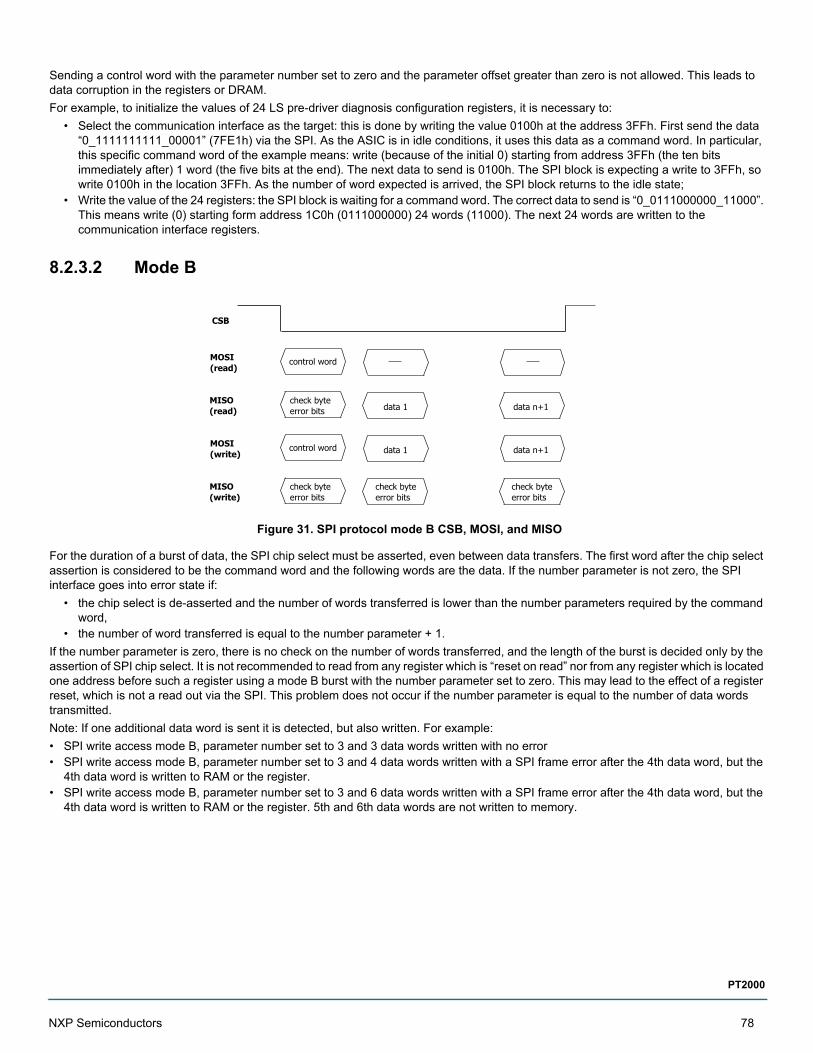
Sending a control word with the parameter number set to zero and the parameter offset greater than zero is not allowed. This leads to data corruption in the registers or DRAM.
For example, to initialize the values of 24 LS pre-driver diagnosis configuration registers, it is necessary to:
• Select the communication interface as the target: this is done by writing the value 0100h at the address 3FFh. First send the data “0_1111111111_00001” (7FE1h) via the SPI. As the ASIC is in idle conditions, it uses this data as a command word. In particular, this specific command word of the example means: write (because of the initial 0) starting from address 3FFh (the ten bits immediately after) 1 word (the five bits at the end). The next data to send is 0100h. The SPI block is expecting a write to 3FFh, so write 0100h in the location 3FFh. As the number of word expected is arrived, the SPI block returns to the idle state;
• Write the value of the 24 registers: the SPI block is waiting for a command word. The correct data to send is “0_0111000000_11000”. This means write (0) starting form address 1C0h (0111000000) 24 words (11000). The next 24 words are written to the communication interface registers.
8.2.3.2 Mode B
Figure 31. SPI protocol mode B CSB, MOSI, and MISO
For the duration of a burst of data, the SPI chip select must be asserted, even between data transfers. The first word after the chip select assertion is considered to be the command word and the following words are the data. If the number parameter is not zero, the SPI interface goes into error state if:
• the chip select is de-asserted and the number of words transferred is lower than the number parameters required by the command word,
• the number of word transferred is equal to the number parameter + 1.
If the number parameter is zero, there is no check on the number of words transferred, and the length of the burst is decided only by the assertion of SPI chip select. It is not recommended to read from any register which is “reset on read” nor from any register which is located one address before such a register using a mode B burst with the number parameter set to zero. This may lead to the effect of a register reset, which is not a read out via the SPI. This problem does not occur if the number parameter is equal to the number of data words transmitted.
Note: If one additional data word is sent it is detected, but also written. For example:
• SPI write access mode B, parameter number set to 3 and 3 data words written with no error• SPI write access mode B, parameter number set to 3 and 4 data words written with a SPI frame error after the 4th data word, but the
4th data word is written to RAM or the register.• SPI write access mode B, parameter number set to 3 and 6 data words written with a SPI frame error after the 4th data word, but the
4th data word is written to RAM or the register. 5th and 6th data words are not written to memory.
CSB
MOSI(read)
control word
MISO(read)
check byteerror bits data 1 data n+1
MOSI(write)
control word
MISO(write)
check byteerror bits
data 1 data n+1
check byteerror bits
check byteerror bits
NXP Semiconductors 78
PT2000
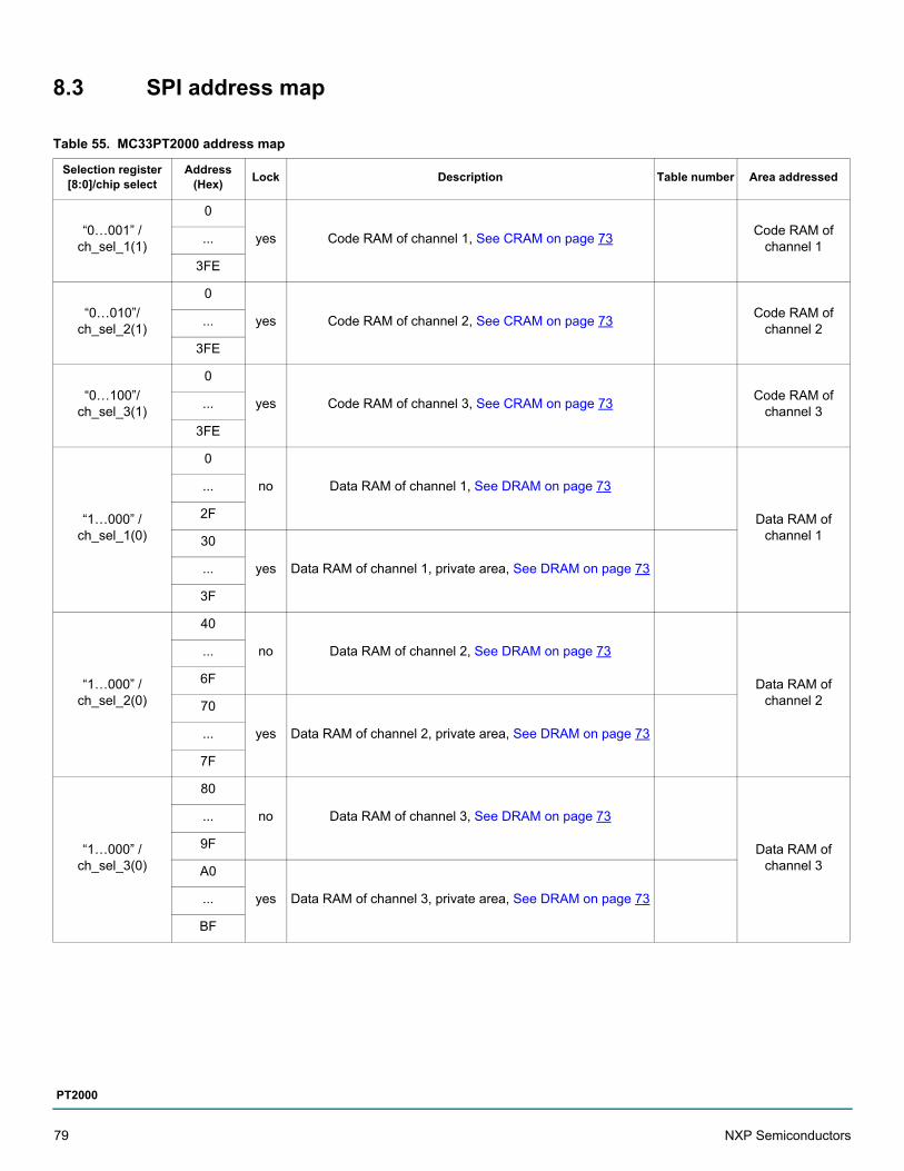
8.3 SPI address map
Table 55. MC33PT2000 address map
Selection register [8:0]/chip select
Address (Hex)
Lock Description Table number Area addressed
“0…001” /ch_sel_1(1)
0
yes Code RAM of channel 1, See CRAM on page 73Code RAM of
channel 1...
3FE
“0…010”/ch_sel_2(1)
0
yes Code RAM of channel 2, See CRAM on page 73Code RAM of
channel 2...
3FE
“0…100”/ch_sel_3(1)
0
yes Code RAM of channel 3, See CRAM on page 73Code RAM of
channel 3...
3FE
“1…000” / ch_sel_1(0)
0
no Data RAM of channel 1, See DRAM on page 73
Data RAM of channel 1
...
2F
30
yes Data RAM of channel 1, private area, See DRAM on page 73...
3F
“1…000” / ch_sel_2(0)
40
no Data RAM of channel 2, See DRAM on page 73
Data RAM of channel 2
...
6F
70
yes Data RAM of channel 2, private area, See DRAM on page 73...
7F
“1…000” / ch_sel_3(0)
80
no Data RAM of channel 3, See DRAM on page 73
Data RAM of channel 3
...
9F
A0
yes Data RAM of channel 3, private area, See DRAM on page 73...
BF
79 NXP Semiconductors
PT2000
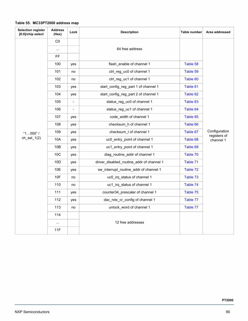
“1…000” /ch_sel_1(2)
C0
64 free address
Configuration registers of channel 1
…
FF
100 yes flash_enable of channel 1 Table 58
101 no ctrl_reg_uc0 of channel 1 Table 59
102 no ctrl_reg_uc1 of channel 1 Table 60
103 yes start_config_reg_part 1 of channel 1 Table 61
104 yes start_config_reg_part 2 of channel 1 Table 62
105 - status_reg_uc0 of channel 1 Table 63
106 - status_reg_uc1 of channel 1 Table 64
107 yes code_width of channel 1 Table 65
108 yes checksum_h of channel 1 Table 66
109 yes checksum_l of channel 1 Table 67
10A yes uc0_entry_point of channel 1 Table 68
10B yes uc1_entry_point of channel 1 Table 69
10C yes diag_routine_addr of channel 1 Table 70
10D yes driver_disabled_routine_addr of channel 1 Table 71
10E yes sw_interrupt_routine_addr of channel 1 Table 72
10F no uc0_irq_status of channel 1 Table 73
110 no uc1_irq_status of channel 1 Table 74
111 yes counter34_prescaler of channel 1 Table 75
112 yes dac_rxtx_cr_config of channel 1 Table 77
113 no unlock_word of channel 1 Table 77
114
12 free addresses...
11F
Table 55. MC33PT2000 address map
Selection register [8:0]/chip select
Address (Hex)
Lock Description Table number Area addressed
NXP Semiconductors 80
PT2000
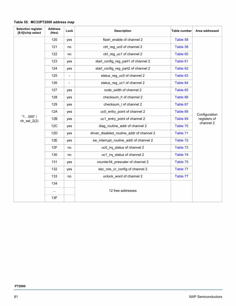
“1…000” /ch_sel_2(2)
120 yes flash_enable of channel 2 Table 58
Configuration registers of channel 2
121 no ctrl_reg_uc0 of channel 2 Table 58
122 no ctrl_reg_uc1 of channel 2 Table 60
123 yes start_config_reg_part1 of channel 2 Table 61
124 yes start_config_reg_part2 of channel 2 Table 62
125 - status_reg_uc0 of channel 2 Table 63
126 - status_reg_uc1 of channel 2 Table 64
127 yes code_width of channel 2 Table 65
128 yes checksum_h of channel 2 Table 66
129 yes checksum_l of channel 2 Table 67
12A yes uc0_entry_point of channel 2 Table 68
12B yes uc1_entry_point of channel 2 Table 69
12C yes diag_routine_addr of channel 2 Table 70
12D yes driver_disabled_routine_addr of channel 2 Table 71
12E yes sw_interrupt_routine_addr of channel 2 Table 72
12F no uc0_irq_status of channel 2 Table 73
130 no uc1_irq_status of channel 2 Table 74
131 yes counter34_prescaler of channel 2 Table 75
132 yes dac_rxtx_cr_config of channel 2 Table 77
133 no unlock_word of channel 2 Table 77
134
12 free addresses...
13F
Table 55. MC33PT2000 address map
Selection register [8:0]/chip select
Address (Hex)
Lock Description Table number Area addressed
81 NXP Semiconductors
PT2000
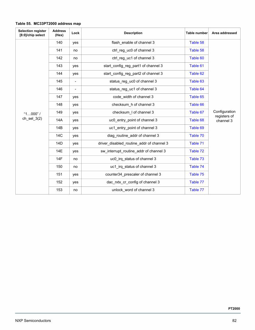
“1…000” /ch_sel_3(2)
140 yes flash_enable of channel 3 Table 58
Configuration registers of channel 3
141 no ctrl_reg_uc0 of channel 3 Table 58
142 no ctrl_reg_uc1 of channel 3 Table 60
143 yes start_config_reg_part1 of channel 3 Table 61
144 yes start_config_reg_part2 of channel 3 Table 62
145 - status_reg_uc0 of channel 3 Table 63
146 - status_reg_uc1 of channel 3 Table 64
147 yes code_width of channel 3 Table 65
148 yes checksum_h of channel 3 Table 66
149 yes checksum_l of channel 3 Table 67
14A yes uc0_entry_point of channel 3 Table 68
14B yes uc1_entry_point of channel 3 Table 69
14C yes diag_routine_addr of channel 3 Table 70
14D yes driver_disabled_routine_addr of channel 3 Table 71
14E yes sw_interrupt_routine_addr of channel 3 Table 72
14F no uc0_irq_status of channel 3 Table 73
150 no uc1_irq_status of channel 3 Table 74
151 yes counter34_prescaler of channel 3 Table 75
152 yes dac_rxtx_cr_config of channel 3 Table 77
153 no unlock_word of channel 3 Table 77
Table 55. MC33PT2000 address map
Selection register [8:0]/chip select
Address (Hex)
Lock Description Table number Area addressed
NXP Semiconductors 82
PT2000
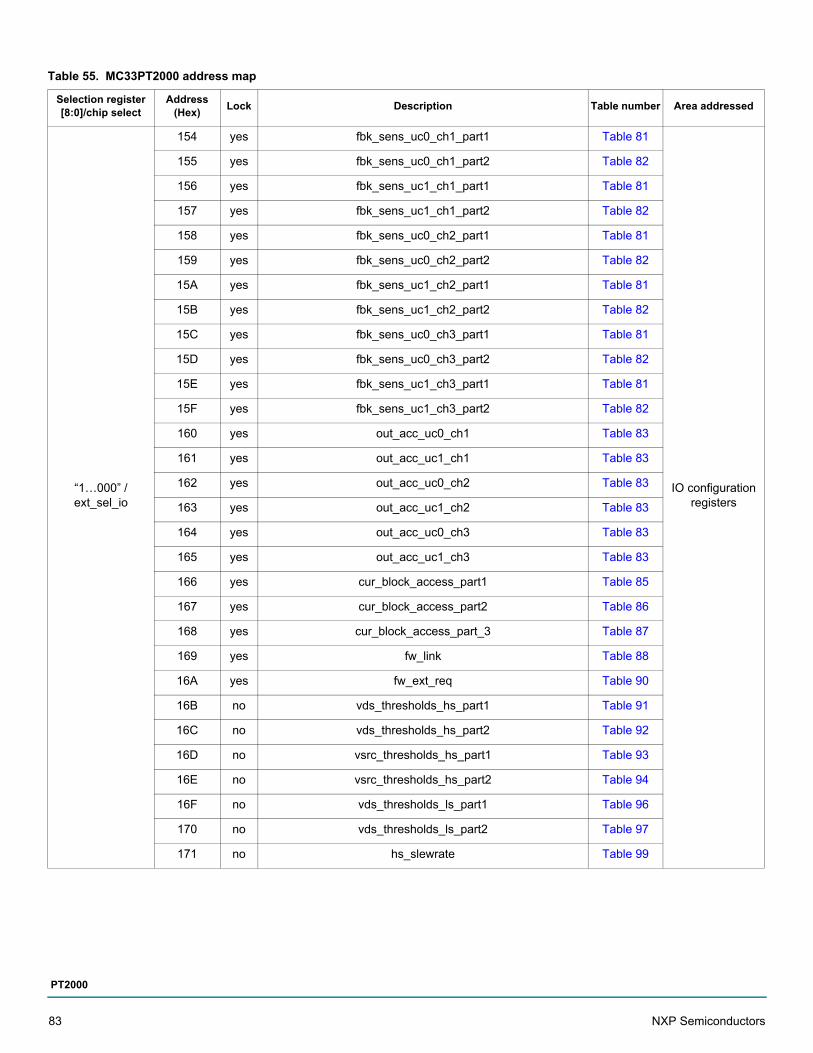
“1…000” /ext_sel_io
154 yes fbk_sens_uc0_ch1_part1 Table 81
IO configuration registers
155 yes fbk_sens_uc0_ch1_part2 Table 82
156 yes fbk_sens_uc1_ch1_part1 Table 81
157 yes fbk_sens_uc1_ch1_part2 Table 82
158 yes fbk_sens_uc0_ch2_part1 Table 81
159 yes fbk_sens_uc0_ch2_part2 Table 82
15A yes fbk_sens_uc1_ch2_part1 Table 81
15B yes fbk_sens_uc1_ch2_part2 Table 82
15C yes fbk_sens_uc0_ch3_part1 Table 81
15D yes fbk_sens_uc0_ch3_part2 Table 82
15E yes fbk_sens_uc1_ch3_part1 Table 81
15F yes fbk_sens_uc1_ch3_part2 Table 82
160 yes out_acc_uc0_ch1 Table 83
161 yes out_acc_uc1_ch1 Table 83
162 yes out_acc_uc0_ch2 Table 83
163 yes out_acc_uc1_ch2 Table 83
164 yes out_acc_uc0_ch3 Table 83
165 yes out_acc_uc1_ch3 Table 83
166 yes cur_block_access_part1 Table 85
167 yes cur_block_access_part2 Table 86
168 yes cur_block_access_part_3 Table 87
169 yes fw_link Table 88
16A yes fw_ext_req Table 90
16B no vds_thresholds_hs_part1 Table 91
16C no vds_thresholds_hs_part2 Table 92
16D no vsrc_thresholds_hs_part1 Table 93
16E no vsrc_thresholds_hs_part2 Table 94
16F no vds_thresholds_ls_part1 Table 96
170 no vds_thresholds_ls_part2 Table 97
171 no hs_slewrate Table 99
Table 55. MC33PT2000 address map
Selection register [8:0]/chip select
Address (Hex)
Lock Description Table number Area addressed
83 NXP Semiconductors
PT2000

“1…000” /ext_sel_io
172 no ls_slewrate_part1 Table 100
IO configuration registers
173 no ls_slewrate_part2 Table 101
174 no offset_compensation12 Table 102
175 no offset_compensation34 Table 103
176 no offset_compensation56 Table 104
177 no adc12_result Table 105
178 no adc34_result Table 106
179 no adc56_result Table 107
17A yes current_filter12 Table 108
17B yes current_filter34 Table 109
17C yes current_filter5l5h Table 110
17D yes current_filter6l6h Table 111
17E yes current_filter5neg6neg Table 112
17F no boost_dac Table 113
180 yes boost_dac_access Table 114
181 yes boost_filter Table 115
182 no vds7_dcdc_config Table 116
183 no vds8_dcdc_config Table 116
184 - batt_result Table 118
185 no dac12_value Table 119
186 no dac34_value Table 120
187 no dac5l5h_value Table 121
188 no dac5neg_value Table 122
189 no dac6l6h_value Table 123
18A no dac6neg_value Table 124
18B no hs_bias_config Table 125
18C no ls_bias_config Table 126
18D - bootstrap_charged Table 127
18E - bootstrap_timer Table 128
18F yes hs1_ls_act Table 131
Table 55. MC33PT2000 address map
Selection register [8:0]/chip select
Address (Hex)
Lock Description Table number Area addressed
NXP Semiconductors 84
PT2000

“1…000” /ext_sel_io
190 yes hs2_ls_act Table 131
IO configuration registers
191 yes hs3_ls_act Table 131
192 yes hs4_ls_act Table 131
193 yes hs5_ls_act Table 131
194 yes hs6_ls_act Table 131
195 yes hs7_ls_act Table 131
196 yes dac_settling_time Table 132
197 no oa_out1_config Table 133
198 no oa_out2_config Table 134
199 no oa_out3_config Table 135
19A
6 free addresses…
19F
Table 55. MC33PT2000 address map
Selection register [8:0]/chip select
Address (Hex)
Lock Description Table number Area addressed
85 NXP Semiconductors
PT2000
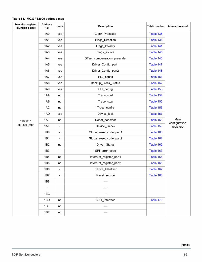
“1000” /ext_sel_mcr
1A0 yes Clock_Prescaler Table 136
Main configuration
registers
1A1 yes Flags_Direction Table 138
1A2 yes Flags_Polarity Table 141
1A3 yes Flags_source Table 145
1A4 yes Offset_compensation_prescaler Table 146
1A5 yes Driver_Config_part1 Table 147
1A6 yes Driver_Config_part2 Table 148
1A7 yes PLL_config Table 151
1A8 yes Backup_Clock_Status Table 152
1A9 yes SPI_config Table 153
1AA no Trace_start Table 154
1AB no Trace_stop Table 155
1AC no Trace_config Table 156
1AD yes Device_lock Table 157
1AE no Reset_behavior Table 158
1AF - Device_unlock Table 159
1B0 - Global_reset_code_part1 Table 160
1B1 - Global_reset_code_part2 Table 161
1B2 no Driver_Status Table 162
1B3 - SPI_error_code Table 163
1B4 no Interrupt_register_part1 Table 164
1B5 no Interrupt_register_part2 Table 165
1B6 - Device_Identifier Table 167
1B7 - Reset_source Table 168
1B8 ----
- ----
1BC ----
1BD no BIST_interface Table 170
1BE no ----
1BF no ----
Table 55. MC33PT2000 address map
Selection register [8:0]/chip select
Address (Hex)
Lock Description Table number Area addressed
NXP Semiconductors 86
PT2000
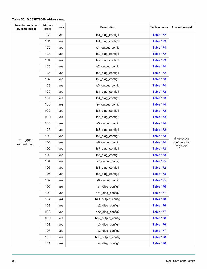
“1…000” /ext_sel_diag
1C0 yes ls1_diag_config1 Table 172
diagnostics configuration
registers
1C1 yes ls1_diag_config2 Table 173
1C2 yes ls1_output_config Table 174
1C3 yes ls2_diag_config1 Table 172
1C4 yes ls2_diag_config2 Table 173
1C5 yes ls2_output_config Table 174
1C6 yes ls3_diag_config1 Table 172
1C7 yes ls3_diag_config2 Table 173
1C8 yes ls3_output_config Table 174
1C9 yes ls4_diag_config1 Table 172
1CA yes ls4_diag_config2 Table 173
1CB yes ls4_output_config Table 174
1CC yes ls5_diag_config1 Table 172
1CD yes ls5_diag_config2 Table 173
1CE yes ls5_output_config Table 174
1CF yes ls6_diag_config1 Table 172
1D0 yes ls6_diag_config2 Table 173
1D1 yes ls6_output_config Table 174
1D2 yes ls7_diag_config1 Table 172
1D3 yes ls7_diag_config2 Table 173
1D4 yes ls7_output_config Table 175
1D5 yes ls8_diag_config1 Table 172
1D6 yes ls8_diag_config2 Table 173
1D7 yes ls8_output_config Table 175
1D8 yes hs1_diag_config1 Table 176
1D9 yes hs1_diag_config2 Table 177
1DA yes hs1_output_config Table 178
1DB yes hs2_diag_config1 Table 176
1DC yes hs2_diag_config2 Table 177
1DD yes hs2_output_config Table 178
1DE yes hs3_diag_config1 Table 176
1DF yes hs3_diag_config2 Table 177
1E0 yes hs3_output_config Table 178
1E1 yes hs4_diag_config1 Table 176
Table 55. MC33PT2000 address map
Selection register [8:0]/chip select
Address (Hex)
Lock Description Table number Area addressed
87 NXP Semiconductors
PT2000
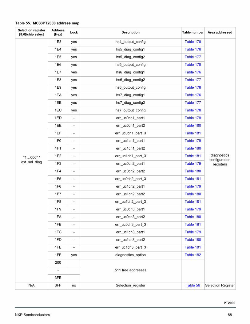
“1…000” /ext_sel_diag
1E3 yes hs4_output_config Table 178
diagnostics configuration
registers
1E4 yes hs5_diag_config1 Table 176
1E5 yes hs5_diag_config2 Table 177
1E6 yes hs5_output_config Table 178
1E7 yes hs6_diag_config1 Table 176
1E8 yes hs6_diag_config2 Table 177
1E9 yes hs6_output_config Table 178
1EA yes hs7_diag_config1 Table 176
1EB yes hs7_diag_config2 Table 177
1EC yes hs7_output_config Table 178
1ED - err_uc0ch1_part1 Table 179
1EE - err_uc0ch1_part2 Table 180
1EF - err_uc0ch1_part_3 Table 181
1F0 - err_uc1ch1_part1 Table 179
1F1 - err_uc1ch1_part2 Table 180
1F2 - err_uc1ch1_part_3 Table 181
1F3 - err_uc0ch2_part1 Table 179
1F4 - err_uc0ch2_part2 Table 180
1F5 - err_uc0ch2_part_3 Table 181
1F6 - err_uc1ch2_part1 Table 179
1F7 - err_uc1ch2_part2 Table 180
1F8 - err_uc1ch2_part_3 Table 181
1F9 - err_uc0ch3_part1 Table 179
1FA - err_uc0ch3_part2 Table 180
1FB - err_uc0ch3_part_3 Table 181
1FC - err_uc1ch3_part1 Table 179
1FD - err_uc1ch3_part2 Table 180
1FE - err_uc1ch3_part_3 Table 181
1FF yes diagnostics_option Table 182
200
511 free addresses-
3FE
N/A 3FF no Selection_register Table 56 Selection Register
Table 55. MC33PT2000 address map
Selection register [8:0]/chip select
Address (Hex)
Lock Description Table number Area addressed
NXP Semiconductors 88
PT2000

8.3.1 Selection register (3FFh)
The selection register is a 4-bit register aimed to select, before starting the read/write operations toward a given address, which internal code RAM is accessed or to select all the other addresses (including the 3 data RAMs and all the registers).
Table 57 details the meaning of the 4 bits in this register. Not all possible values are allowed for this register.
This selection register is accessible at address 3FFh and is the only register accessed anyway from the SPI, whatever the value of the selection register. This means address 3FFh can only be used for this purpose, even if any of the code RAMs is selected, so each 1024x16 code RAM in the MC33PT2000 can actually only store 1023 data. Note that 2 or 3 code RAMs can be written in parallel during normal mode.
Table 56. selection_register (3FFh)
Bit 15 14 13 12 11 10 9 8 7 6 5 4 3 2 1 0
Name Reservedcomm.page sel
ReservedCRAM_ch3_sel
CRAM_ch2_sel
CRAM_ch1_sel
R/W - r/w - r/w r/w r/w
Lock - no - no no no
Reset 0000000 0 00000 0 0 0
Table 57. Selection register
Selection register comm. page sel
Selection register CRAM chx
Element addressed
‘0’ “000” Nothing selected. Further SPI operation, except for the one concerning this register is ignored.
‘0’ “001” Channel 1 Code RAM selected
‘0’ “010” Channel 2 Code RAM selected
‘0’ “100” Channel 3 Code RAM selected
‘0’ “011” Write operation affects the Code RAM of channel 1 and 2. Read operation is not possible.
‘0’ “101” Write operation affects the Code RAM of channel 1 and 3. Read operation is not possible.
‘0’ “110” Write operation affects the Code RAM of channel 2 and 3. Read operation is not possible.
‘0’ “111” Write operation affects the all three channel’s Code RAM. Read operation is not possible.
‘1’ d.c. Common page selected. The lower three bits are ignored. “100000000” is written to the register.
89 NXP Semiconductors
PT2000
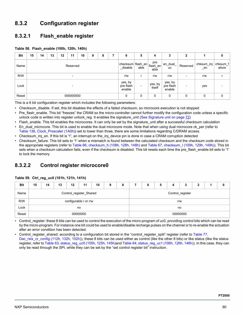
8.3.2 Configuration register
8.3.2.1 Flash_enable register
This is a 6 bit configuration register which includes the following parameters:
• Checksum_disable. If set, this bit disables the effects of a failed checksum, so microcore execution is not stopped• Pre_flash_enable. This bit “freezes” the CRAM so the micro-controller cannot further modify the configuration code unless a specific
unlock code is written into register unlock_reg. It enables the signature_unit (See Signature unit on page 72)• Flash_enable. This bit enables the microcores. It can only be set by the signature_unit after a successful checksum calculation• En_dual_microcore. This bit is used to enable the dual microcore mode. Note that when using dual microcore ck_per (refer to
Table 136, Clock_Prescaler (1A0h)) set to lower than three, there are some limitations regarding C/DRAM access.• Checksum_irq_en. If this bit is '1', an interrupt on the_irq_device pin is done in case a CRAM corruption detected• Checksum_failure. This bit sets to '1' when a mismatch is found between the calculated checksum and the checksum code stored in
the appropriate registers (refer to Table 66, checksum_h (108h, 128h, 148h) and Table 67, checksum_l (109h, 129h, 149h)). This bit sets when a checksum calculation fails, even if the checksum is disabled. This bit resets each time the pre_flash_enable bit sets to '1' to lock the memory.
8.3.2.2 Control register microcore0
• Control_register: these 8 bits can be used to control the execution of the micro-program of uc0, providing control bits which can be read by the micro-program. For instance one bit could be used to enable/disable recharge pulses on the channel or to re-enable the actuation after an error condition has been detected.
• Control_register_shared: according to a configuration bit stored in the “control_register_split” register (refer to Table 77, Dac_rxtx_cr_config (112h, 132h, 152h)), these 8 bits can be used either as control (like the other 8 bits) or like status (like the status register, refer to Table 63, status_reg_uc0 (105h, 125h, 145h)and Table 64, status_reg_uc1 (106h, 126h, 146h)). In this case, they can only be read through the SPI, while they can be set by the “set control register bit” instruction.
Table 58. Flash_enable (100h, 120h, 140h)
Bit 15 14 13 12 11 10 9 8 7 6 5 4 3 2 1 0
Name Reservedchecksum_disable
flash_enable
pre flash_en
able
en_dual_uc
Reservedchksum_irq
_enchksum_f
ailure
R/W - r/w r r/w r/w - r/w r
Lock -yes, by
pre flash enable
-yes, by itself
yes, by pre flash enable
- yes -
Reset 000000000 0 0 0 0 0 0 0
Table 59. Ctrl_reg_uc0 (101h, 121h, 141h)
Bit 15 14 13 12 11 10 9 8 7 6 5 4 3 2 1 0
Name Control_register_Shared Control_register
R/W configurable r or r/w r/w
Lock no no
Reset 00000000 00000000
NXP Semiconductors 90
PT2000
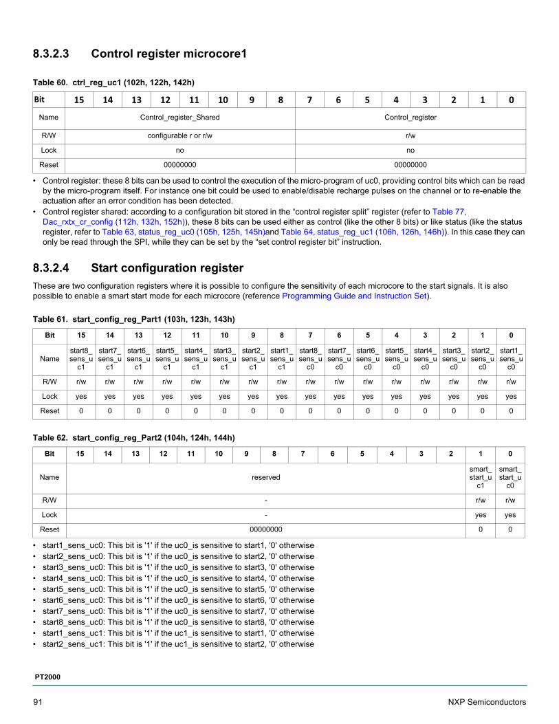
8.3.2.3 Control register microcore1
• Control register: these 8 bits can be used to control the execution of the micro-program of uc0, providing control bits which can be read by the micro-program itself. For instance one bit could be used to enable/disable recharge pulses on the channel or to re-enable the actuation after an error condition has been detected.
• Control register shared: according to a configuration bit stored in the “control register split” register (refer to Table 77, Dac_rxtx_cr_config (112h, 132h, 152h)), these 8 bits can be used either as control (like the other 8 bits) or like status (like the status register, refer to Table 63, status_reg_uc0 (105h, 125h, 145h)and Table 64, status_reg_uc1 (106h, 126h, 146h)). In this case they can only be read through the SPI, while they can be set by the “set control register bit” instruction.
8.3.2.4 Start configuration register
These are two configuration registers where it is possible to configure the sensitivity of each microcore to the start signals. It is also possible to enable a smart start mode for each microcore (reference Programming Guide and Instruction Set).
• start1_sens_uc0: This bit is '1' if the uc0_is sensitive to start1, '0' otherwise• start2_sens_uc0: This bit is '1' if the uc0_is sensitive to start2, '0' otherwise• start3_sens_uc0: This bit is '1' if the uc0_is sensitive to start3, '0' otherwise• start4_sens_uc0: This bit is '1' if the uc0_is sensitive to start4, '0' otherwise• start5_sens_uc0: This bit is '1' if the uc0_is sensitive to start5, '0' otherwise• start6_sens_uc0: This bit is '1' if the uc0_is sensitive to start6, '0' otherwise• start7_sens_uc0: This bit is '1' if the uc0_is sensitive to start7, '0' otherwise• start8_sens_uc0: This bit is '1' if the uc0_is sensitive to start8, '0' otherwise• start1_sens_uc1: This bit is '1' if the uc1_is sensitive to start1, '0' otherwise• start2_sens_uc1: This bit is '1' if the uc1_is sensitive to start2, '0' otherwise
Table 60. ctrl_reg_uc1 (102h, 122h, 142h)
Bit 15 14 13 12 11 10 9 8 7 6 5 4 3 2 1 0
Name Control_register_Shared Control_register
R/W configurable r or r/w r/w
Lock no no
Reset 00000000 00000000
Table 61. start_config_reg_Part1 (103h, 123h, 143h)
Bit 15 14 13 12 11 10 9 8 7 6 5 4 3 2 1 0
Namestart8_sens_u
c1
start7_sens_u
c1
start6_sens_u
c1
start5_sens_u
c1
start4_sens_u
c1
start3_sens_u
c1
start2_sens_u
c1
start1_sens_u
c1
start8_sens_u
c0
start7_sens_u
c0
start6_sens_u
c0
start5_sens_u
c0
start4_sens_u
c0
start3_sens_u
c0
start2_sens_u
c0
start1_sens_u
c0
R/W r/w r/w r/w r/w r/w r/w r/w r/w r/w r/w r/w r/w r/w r/w r/w r/w
Lock yes yes yes yes yes yes yes yes yes yes yes yes yes yes yes yes
Reset 0 0 0 0 0 0 0 0 0 0 0 0 0 0 0 0
Table 62. start_config_reg_Part2 (104h, 124h, 144h)
Bit 15 14 13 12 11 10 9 8 7 6 5 4 3 2 1 0
Name reservedsmart_start_u
c1
smart_start_u
c0
R/W - r/w r/w
Lock - yes yes
Reset 00000000 0 0
91 NXP Semiconductors
PT2000
• start3_sens_uc1: This bit is '1' if the uc1_is sensitive to start3, '0' otherwise• start4_sens_uc1: This bit is '1' if the uc1_is sensitive to start4, '0' otherwise• start5_sens_uc1: This bit is '1' if the uc1_is sensitive to start5, '0' otherwise• start6_sens_uc1: This bit is '1' if the uc1_is sensitive to start6, '0' otherwise• start7_sens_uc1: This bit is '1' if the uc1_is sensitive to start7, '0' otherwise• start8_sens_uc1: This bit is '1' if the uc1_is sensitive to start8, '0' otherwise• smart_start_uc0: This bit is '1' if the smart start mode is enabled for uc0, '0' otherwise (reference Programming Guide and Instruction
Set).• smart_start_uc1: This bit is '1' if the smart start mode is enabled for uc1, '0' otherwise (reference Programming Guide and Instruction
Set).
8.3.2.5 Status register microcore0
This 16-bit register is a read-only register and only provides information about the uc0_status to the external microcontroller. The register can be used to exchange application dependent information (status bits, for instance regarding the execution phase of the micro-program, diagnostics results) between the microcore and the main microcontroller according to the way the micro-program is designed. The registers can be configured so they reset after a SPI read operation to the register (see Table 158, Reset_Behavior (1AEh)).
8.3.2.6 Status register microcore1
This 16-bit register is a read-only register and only provides information about the uc1_status to the external microcontroller. The register can be used to exchange application dependent information (status bits, for instance regarding the execution phase of the micro-program) between the microcore and the main microcontroller according to the way the micro-program is designed. The registers can be configured so they reset after a SPI read operation to the register (see Table 158, Reset_Behavior (1AEh)).
Table 63. status_reg_uc0 (105h, 125h, 145h)
Bit 15 14 13 12 11 10 9 8 7 6 5 4 3 2 1 0
Name status_register
R/W r
Lock -
Reset on read
configurable
Reset 0000000000000000
Table 64. status_reg_uc1 (106h, 126h, 146h)
Bit 15 14 13 12 11 10 9 8 7 6 5 4 3 2 1 0
Name status_register
R/W r
Lock -
Reset on read
configurable
Reset 0000000000000000
NXP Semiconductors 92
PT2000
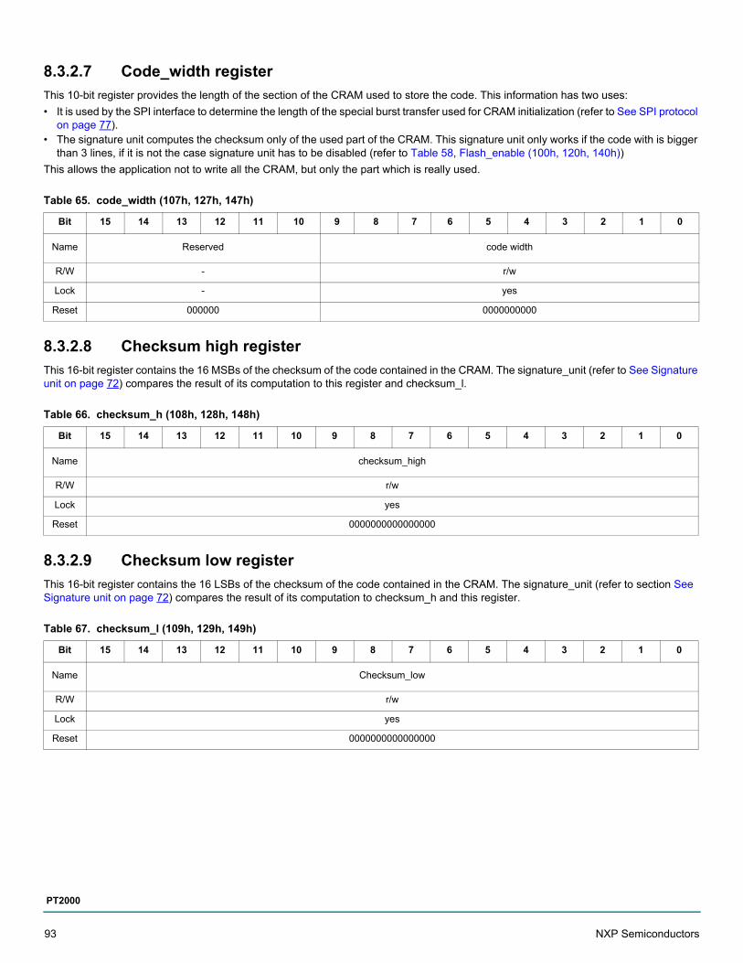
8.3.2.7 Code_width register
This 10-bit register provides the length of the section of the CRAM used to store the code. This information has two uses:
• It is used by the SPI interface to determine the length of the special burst transfer used for CRAM initialization (refer to See SPI protocol on page 77).
• The signature unit computes the checksum only of the used part of the CRAM. This signature unit only works if the code with is bigger than 3 lines, if it is not the case signature unit has to be disabled (refer to Table 58, Flash_enable (100h, 120h, 140h))
This allows the application not to write all the CRAM, but only the part which is really used.
8.3.2.8 Checksum high register
This 16-bit register contains the 16 MSBs of the checksum of the code contained in the CRAM. The signature_unit (refer to See Signature unit on page 72) compares the result of its computation to this register and checksum_l.
8.3.2.9 Checksum low register
This 16-bit register contains the 16 LSBs of the checksum of the code contained in the CRAM. The signature_unit (refer to section See Signature unit on page 72) compares the result of its computation to checksum_h and this register.
Table 65. code_width (107h, 127h, 147h)
Bit 15 14 13 12 11 10 9 8 7 6 5 4 3 2 1 0
Name Reserved code width
R/W - r/w
Lock - yes
Reset 000000 0000000000
Table 66. checksum_h (108h, 128h, 148h)
Bit 15 14 13 12 11 10 9 8 7 6 5 4 3 2 1 0
Name checksum_high
R/W r/w
Lock yes
Reset 0000000000000000
Table 67. checksum_l (109h, 129h, 149h)
Bit 15 14 13 12 11 10 9 8 7 6 5 4 3 2 1 0
Name Checksum_low
R/W r/w
Lock yes
Reset 0000000000000000
93 NXP Semiconductors
PT2000
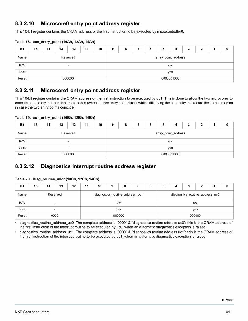
8.3.2.10 Microcore0 entry point address register
This 10-bit register contains the CRAM address of the first instruction to be executed by microcontroller0.
8.3.2.11 Microcore1 entry point address register
This 10-bit register contains the CRAM address of the first instruction to be executed by uc1. This is done to allow the two microcores to execute completely independent microcodes (when the two entry point differ), while still having the capability to execute the same program in case the two entry points coincide.
8.3.2.12 Diagnostics interrupt routine address register
• diagnostics_routine_address_uc0. The complete address is “0000” & “diagnostics routine address uc0”: this is the CRAM address of the first instruction of the interrupt routine to be executed by uc0_when an automatic diagnostics exception is raised.
• diagnostics_routine_address_uc1. The complete address is “0000” & “diagnostics routine address uc1”: this is the CRAM address of the first instruction of the interrupt routine to be executed by uc1_when an automatic diagnostics exception is raised.
Table 68. uc0_entry_point (10Ah, 12Ah, 14Ah)
Bit 15 14 13 12 11 10 9 8 7 6 5 4 3 2 1 0
Name Reserved entry_point_address
R/W - r/w
Lock - yes
Reset 000000 0000001000
Table 69. uc1_entry_point (10Bh, 12Bh, 14Bh)
Bit 15 14 13 12 11 10 9 8 7 6 5 4 3 2 1 0
Name Reserved entry_point_address
R/W - r/w
Lock - yes
Reset 000000 0000001000
Table 70. Diag_routine_addr (10Ch, 12Ch, 14Ch)
Bit 15 14 13 12 11 10 9 8 7 6 5 4 3 2 1 0
Name Reserved diagnostics_routine_address_uc1 diagnostics_routine_address_uc0
R/W - r/w r/w
Lock - yes yes
Reset 0000 000000 000000
NXP Semiconductors 94
PT2000
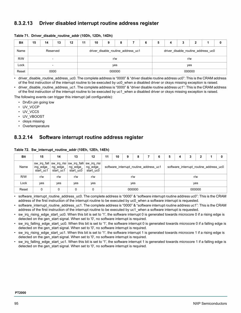
8.3.2.13 Driver disabled interrupt routine address register
• driver_disable_routine_address_uc0. The complete address is “0000” & “driver disable routine address uc0”: This is the CRAM address of the first instruction of the interrupt routine to be executed by uc0_when a disabled driver or cksys missing exception is raised.
• driver_disable_routine_address_uc1. The complete address is “0000” & “driver disable routine address uc1”: This is the CRAM address of the first instruction of the interrupt routine to be executed by uc1_when a disabled driver or cksys missing exception is raised.
The following events can trigger this interrupt (all configurable):
• DrvEn pin going low• UV_VCCP• UV_VCC5• UV_VBOOST• cksys missing• Overtemperature
8.3.2.14 Software interrupt routine address register
• software_interrupt_routine_address_uc0. The complete address is “0000” & “software interrupt routine address uc0”: This is the CRAM address of the first instruction of the interrupt routine to be executed by uc0_when a software interrupt is requested.
• software_interrupt_routine_address_uc1. The complete address is “0000” & “software interrupt routine address uc1”: This is the CRAM address of the first instruction of the interrupt routine to be executed by uc1_when a software interrupt is requested.
• sw_irq_rising_edge_start_uc0. When this bit is set to '1', the software interrupt 0 is generated towards microcore 0 if a rising edge is detected on the gen_start signal. When set to '0', no software interrupt is required.
• sw_irq_falling_edge_start_uc0. When this bit is set to '1', the software interrupt 0 is generated towards microcore 0 if a falling edge is detected on the gen_start signal. When set to '0', no software interrupt is required.
• sw_irq_rising_edge_start_uc1. When this bit is set to '1', the software interrupt 1 is generated towards microcore 1 if a rising edge is detected on the gen_start signal. When set to '0', no software interrupt is required.
• sw_irq_falling_edge_start_uc1. When this bit is set to '1', the software interrupt 1 is generated towards microcore 1 if a falling edge is detected on the gen_start signal. When set to '0', no software interrupt is required.
Table 71. Driver_disable_routine_addr (10Dh, 12Dh, 14Dh)
Bit 15 14 13 12 11 10 9 8 7 6 5 4 3 2 1 0
Name Reserved driver_disable_routine_address_uc1 driver_disable_routine_address_uc0
R/W - r/w r/w
Lock - yes yes
Reset 0000 000000 000000
Table 72. Sw_interrupt_routine_addr (10Eh, 12Eh, 14Eh)
Bit 15 14 13 12 11 10 9 8 7 6 5 4 3 2 1 0
Namesw_irq_falling_edge_start_uc1
sw_irq_rising_edge_start_uc1
sw_irq_falling_edge_start_uc0
sw_irq_rising_edge_start_uc0
software_interrupt_routine_address_uc1 software_interrupt_routine_address_uc0
R/W r/w r/w r/w r/w r/w r/w
Lock yes yes yes yes yes yes
Reset 0 0 0 0 000000 000000
95 NXP Semiconductors
PT2000
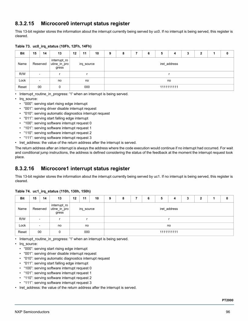
8.3.2.15 Microcore0 interrupt status register
This 13-bit register stores the information about the interrupt currently being served by uc0. If no interrupt is being served, this register is cleared.
• Interrupt_routine_in_progress: '1' when an interrupt is being served.• Irq_source:
• “000”: serving start rising edge interrupt• “001”: serving driver disable interrupt request• “010”: serving automatic diagnostics interrupt request• “011”: serving start falling edge interrupt• “100”: serving software interrupt request 0• “101”: serving software interrupt request 1• “110”: serving software interrupt request 2• “111”: serving software interrupt request 3
• Iret_address: the value of the return address after the interrupt is served.
The return address after an interrupt is always the address where the code execution would continue if no interrupt had occurred. For wait and conditional jump instructions, the address is defined considering the status of the feedback at the moment the interrupt request took place.
8.3.2.16 Microcore1 interrupt status register
This 13-bit register stores the information about the interrupt currently being served by uc1. If no interrupt is being served, this register is cleared.
• Interrupt_routine_in_progress: '1' when an interrupt is being served.• Irq_source:
• “000”: serving start rising edge interrupt• “001”: serving driver disable interrupt request• “010”: serving automatic diagnostics interrupt request• “011”: serving start falling edge interrupt• “100”: serving software interrupt request 0• “101”: serving software interrupt request 1• “110”: serving software interrupt request 2• “111”: serving software interrupt request 3
• Iret_address: the value of the return address after the interrupt is served.
Table 73. uc0_irq_status (10Fh, 12Fh, 14Fh)
Bit 15 14 13 12 11 10 9 8 7 6 5 4 3 2 1 0
Name Reservedinterrupt_routine_in_pro
gressirq_source iret_address
R/W - r r r
Lock - no no no
Reset 00 0 000 1111111111
Table 74. uc1_irq_status (110h, 130h, 150h)
Bit 15 14 13 12 11 10 9 8 7 6 5 4 3 2 1 0
Name Reservedinterrupt_routine_in_pro
gressirq_source iret_address
R/W - r r r
Lock - no no no
Reset 00 0 000 1111111111
NXP Semiconductors 96
PT2000
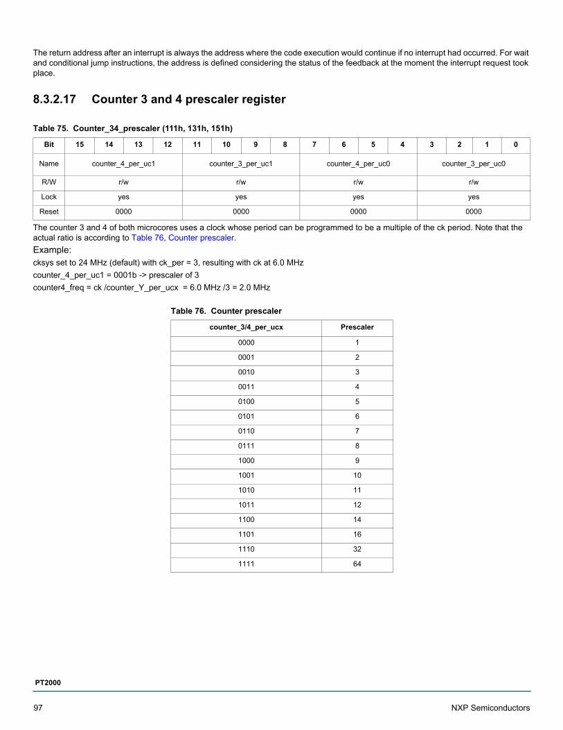
The return address after an interrupt is always the address where the code execution would continue if no interrupt had occurred. For wait and conditional jump instructions, the address is defined considering the status of the feedback at the moment the interrupt request took place.
8.3.2.17 Counter 3 and 4 prescaler register
The counter 3 and 4 of both microcores uses a clock whose period can be programmed to be a multiple of the ck period. Note that the actual ratio is according to Table 76, Counter prescaler.
Example: cksys set to 24 MHz (default) with ck_per = 3, resulting with ck at 6.0 MHz
counter_4_per_uc1 = 0001b -> prescaler of 3
counter4_freq = ck /counter_Y_per_ucx = 6.0 MHz /3 = 2.0 MHz
Table 75. Counter_34_prescaler (111h, 131h, 151h)
Bit 15 14 13 12 11 10 9 8 7 6 5 4 3 2 1 0
Name counter_4_per_uc1 counter_3_per_uc1 counter_4_per_uc0 counter_3_per_uc0
R/W r/w r/w r/w r/w
Lock yes yes yes yes
Reset 0000 0000 0000 0000
Table 76. Counter prescaler
counter_3/4_per_ucx Prescaler
0000 1
0001 2
0010 3
0011 4
0100 5
0101 6
0110 7
0111 8
1000 9
1001 10
1010 11
1011 12
1100 14
1101 16
1110 32
1111 64
97 NXP Semiconductors
PT2000

8.3.2.18 DAC Rxtx configuration register
Each microcore can only access four out of six current measurement channel DACs via the internal address map. In addition, either the two special DACs of current measurement channel five or six can be used. The two DACs linked to their own channel can always be addressed via sssc and ossc. In addition, the two DACs of one other channel can be addressed via the ssoc and osoc parameter. It can be decided by register bits or microcode instruction slocdac for each microcore, which of the two other channels (next channel or previous channel), DACs are accessible and if DACs H and NEG of channel five or six are accessible.
Only one microcore can be addressed at the same time in the channel communication register (rxtx register in the memory map). This can be decided by register bits or microcode instruction sl56dac.
• CR_shared_uc0: if set to '0', all 16 of the bits of the control register uc0_are used as control bits. If set to '1', the 8 MSBs of the control register (control register shared) are used as status bits.
• CR_shared_uc1: if set to '0', all 16 of the bits of the control register uc1_are used as control bits. If set to '1', the 8 MSBs of the control register (control register shared) are used as status bits.
• oc_dac_sel_uc0: selects the other dac for microcore 0.• ‘0', channel 1: ssoc refers to dac3, osoc refers to dac4 (next channel = 2)• ‘0', channel 2: ssoc refers to dac5, osoc refers to dac6 (next channel = 3)• ‘0', channel 3: ssoc refers to dac1, osoc refers to dac2 (next channel = 1)• ‘1', channel 1: ssoc refers to dac5, osoc refers to dac6 (prev. channel = 3)• ‘1', channel 2: ssoc refers to dac1, osoc refers to dac2 (prev. channel = 1)• ‘1', channel 3: ssoc refers to dac3, osoc refers to dac4 (prev. channel = 2)
• oc_dac_sel_uc1: selects the other dac for microcore 1.• '0', channel 1: ssoc refers to dac4, osoc refers to dac3 (next channel = 2)• '0', channel 2: ssoc refers to dac6, osoc refers to dac5 (next channel = 3)• '0', channel 3: ssoc refers to dac2, osoc refers to dac1 (next channel = 1)• '1', channel 1: ssoc refers to dac6, osoc refers to dac5 (prev. channel = 3)• '1', channel 2: ssoc refers to dac2, osoc refers to dac1 (prev. channel = 1)• '1', channel 3: ssoc refers to dac4, osoc refers to dac3 (prev. channel = 2)
• dac56_sel_ucX: selects the dac5/6 for microcore X.• '0': dac56h56n refers to dac5• '1': dac56h56n refers to dac6
Table 77. Dac_rxtx_cr_config (112h, 132h, 152h)
Bit 15 14 13 12 11 10 9 8 7 6 5 4 3 2 1 0
Name Reserved rxtx_link_sel_uc1 rxtx_link_sel_uc0 Reserveddac56_sel_uc1
dac56_sel_uc0
oc_dac_sel_uc
1
oc_dac_sel_uc
0
CR_shared_u
c1
CR_shared_u
c0
R/W - r/w r/w - r/w r/w r/w r/w r/w r/w
Lock - no no - no no no no yes yes
Reset 00 000 000 00 0 0 0 0 0 0
Table 78. Other dac configuration
Microcore dac sssc dac osscoc_dac_sel_ucX =’0’ (next channel) oc_dac_sel_ucX =’1’ (previous channel)
dac ssoc dac osoc dac ssoc dac osoc
uc0, channel 1 dac1 dac2 dac3 dac4 dac5 dac6
uc1, channel 1 dac2 dac1 dac4 dac3 dac6 dac5
uc0, channel 2 dac3 dac4 dac5 dac6 dac1 dac2
uc1, channel 2 dac4 dac3 dac6 dac5 dac2 dac1
uc0, channel 3 dac5 dac6 dac1 dac2 dac3 dac4
uc1, channel 3 dac6 dac5 dac2 dac1 dac4 dac3
NXP Semiconductors 98
PT2000
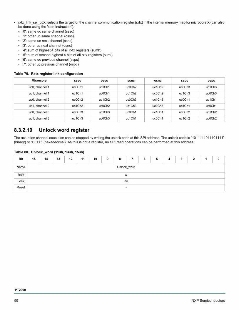
• rxtx_link_sel_ucX: selects the target for the channel communication register (rxtx) in the internal memory map for microcore X (can also be done using the 'stcrt instruction').• '0': same uc same channel (sssc)• '1': other uc same channel (ossc)• '2': same uc next channel (ssnc)• '3': other uc next channel (osnc)• '4': sum of highest 4 bits of all rxtx registers (sumh)• '5': sum of second highest 4 bits of all rxtx registers (suml)• '6': same uc previous channel (sspc)• '7': other uc previous channel (ospc)
8.3.2.19 Unlock word register
The actuation channel execution can be stopped by writing the unlock code at this SPI address. The unlock code is “1011111011101111” (binary) or “BEEF” (hexadecimal). As this is not a register, no SPI read operations can be performed at this address.
Table 79. Rxtx register link configuration
Microcore sssc ossc ssnc osnc sspc ospc
uc0, channel 1 uc0Ch1 uc1Ch1 uc0Ch2 uc1Ch2 uc0Ch3 uc1Ch3
uc1, channel 1 uc1Ch1 uc0Ch1 uc1Ch2 uc0Ch2 uc1Ch3 uc0Ch3
uc0, channel 2 uc0Ch2 uc1Ch2 uc0Ch3 uc1Ch3 uc0Ch1 uc1Ch1
uc1, channel 2 uc1Ch2 uc0Ch2 uc1Ch3 uc0Ch3 uc1Ch1 uc0Ch1
uc0, channel 3 uc0Ch3 uc1Ch3 uc0Ch1 uc1Ch1 uc0Ch2 uc1Ch2
uc1, channel 3 uc1Ch3 uc0Ch3 uc1Ch1 uc0Ch1 uc1Ch2 uc0Ch2
Table 80. Unlock_word (113h, 133h, 153h)
Bit 15 14 13 12 11 10 9 8 7 6 5 4 3 2 1 0
Name Unlock_word
R/W w
Lock no
Reset -
99 NXP Semiconductors
PT2000

8.3.3 IO configuration registers
8.3.3.1 Feedback microcore sensitivities registers
These 12 registers (two for each microcore). Select the feedback to which each microcore is sensitive (e.g. configures if ucX chY is sensitive to VDS errors on HS1).
8.3.3.2 Microcores output access registers
These six registers are designed to provide access rights to manage the control signals (output_command, VDS threshold, VSRC threshold, fw auto, en_halt_x) of each output block to the required microcores. Each bit controls the access from one microcore to manage the control signals of an output: if the value is set to 1, the microcore can drive the control signals (output_command, VDS threshold, VSRC threshold, fw auto, en_halt_x), otherwise access is denied.
The requests coming from the microcores are not continuous; instead the microcores perform a request each time a change to a control signal (output_command, VDS threshold, VSRC threshold, fw auto, en_halt_x) is required. If multiple microcores have access to the same output block, as a shared resource, this block is able to handle the collision: if more than one microcore wants to change one of the control signals in the same ck cycle, priorities are used as defined in Table 84, Out_acc_ucxchy collision handling.
If one of the microcores which have access to a pre-driver not locked, the other microcore can switch on the pre-driver for only one ck cycle maximum. After one ck cycle the output is switched off again, because this request comes from the disabled microcore. This is a safety feature of the device. If requests to change a control signal are received from different microcores (assuming both have access rights) in different ck cycles, all the requested changes are applied in sequence.
Table 81. Fbk_sens_ucxchy_part1 (154h, 156h, 158h, 15Ah, 15Ch, 15Eh)
Bit 15 14 13 12 11 10 9 8 7 6 5 4 3 2 1 0
NameReserv
ed
Hs7_Vsrc_se
ns
Hs6_Vsrc_se
ns
Hs5_Vsrc_se
ns
Hs4_Vsrc_se
ns
Hs3_Vsrc_se
ns
Hs2_Vsrc_se
ns
Hs1_Vsrc_se
ns
Reserved
Hs7_Vsd_sen
s
Hs6_Vsd_sen
s
Hs5_Vsd_sen
s
Hs4_Vsd_sen
s
Hs3_Vsd_sen
s
Hs2_Vsd_sen
s
Hs1_Vsd_sen
s
R/W - r/w r/w r/w r/w r/w r/w r/w - r/w r/w r/w r/w r/w r/w r/w
Lock - yes yes yes yes yes yes yes - yes yes yes yes yes yes yes
Reset 0 0 0 0 0 0 0 0 0 0 0 0 0 0 0 0
Table 82. Fbk_sens_ucxchy_part2 (155h, 157h, 159h, 15Bh, 15Dh, 15Fh)
Bit 15 14 13 12 11 10 9 8 7 6 5 4 3 2 1 0
Name ReservedLs8_Vds_sens
Ls7_Vds_sen
s
Ls6_Vds_sens
Ls5_Vds_sens
Ls4_Vds_sens
Ls3_Vds_sens
Ls2_Vds_sens
Ls1_Vds_sen
s
R/W - r/w r/w r/w r/w r/w r/w r/w r/w
Lock - yes yes yes yes yes yes yes yes
Reset 00000000 0 0 0 0 0 0 0 0
Table 83. Out_acc_ucx_chy (160h, 161h, 162h, 163h, 164h, 165h)
Bit 15 14 13 12 11 10 9 8 7 6 5 4 3 2 1 0
NameAcc_ucX_chY_ls8
Acc_ucX_chY_ls7
Acc_ucX_chY_ls6
Acc_ucX_chY_ls5
Acc_ucX_chY_ls4
Acc_ucX_chY_ls3
Acc_ucX_chY
_ls2
Acc_ucX_chY_ls1
Reserved
Acc_ucX_chY_hs7
Acc_ucX_chY_hs6
Acc_ucX_chY_hs5
Acc_ucX_chY_hs4
Acc_ucX_chY_hs3
Acc_ucX_chY_hs2
Acc_ucX_chY_hs1
R/W r/w r/w r/w r/w r/w r/w r/w r/w - r/w r/w r/w r/w r/w r/w r/w
Lock yes yes yes yes yes yes yes yes - yes yes yes yes yes yes yes
Reset 0 0 0 0 0 0 0 0 0 0 0 0 0 0 0 0
NXP Semiconductors 100
PT2000
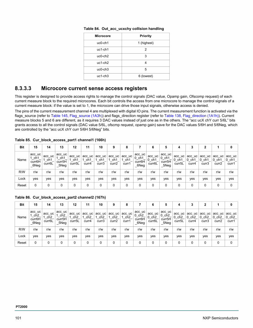
8.3.3.3 Microcore current sense access registers
This register is designed to provide access rights to manage the control signals (DAC value, Opamp gain, Ofscomp request) of each current measure block to the required microcores. Each bit controls the access from one microcore to manage the control signals of a current measure block: if the value is set to 1, the microcore can drive those input signals, otherwise access is denied.
The pins of the current measurement channel 4 are multiplexed with digital IO pins. The current measurement function is activated via the flags_source (refer to Table 145, Flag_source (1A3h)) and flags_direction register (refer to Table 138, Flag_direction (1A1h)). Current measure blocks 5 and 6 are different, as it requires 3 DAC values instead of just one as in the others. The “acc ucX chY curr 5/6L” bits grants access to all the control signals (DAC value 5/6L, ofscmp request, opamp gain) save for the DAC values 5/6H and 5/6Neg, which are controlled by the “acc ucX chY curr 5/6H 5/6Neg” bits.
Table 84. Out_acc_ucxchy collision handling
Microcore Priority
uc0-ch1 1 (highest)
uc1-ch1 2
uc0-ch2 3
uc1-ch2 4
uc0-ch3 5
uc1-ch3 6 (lowest)
Table 85. Cur_block_access_part1 channel1 (166h)
Bit 15 14 13 12 11 10 9 8 7 6 5 4 3 2 1 0
Name
acc_uc1_ch1_curr6H_6Neg
acc_uc1_ch1_curr6L
acc_uc1_ch1_curr5H_5Neg
acc_uc1_ch1_curr5L
acc_uc1_ch1_curr4
acc_uc1_ch1_curr3
acc_uc1_ch1_curr2
acc_uc1_ch1_curr1
acc_uc0_ch1_curr6H_6Neg
acc_uc0_ch1_curr6L
acc_uc0_ch1_curr5H_5Neg
acc_uc0_ch1_curr5L
acc_uc0_ch1_curr4
acc_uc0_ch1_curr3
acc_uc0_ch1_curr2
acc_uc0_ch1_curr1
R/W r/w r/w r/w r/w r/w r/w r/w r/w r/w r/w r/w r/w r/w r/w r/w r/w
Lock yes yes yes yes yes yes yes yes yes yes yes yes yes yes yes yes
Reset 0 0 0 0 0 0 0 0 0 0 0 0 0 0 0 0
Table 86. Cur_block_access_part2 channel2 (167h)
Bit 15 14 13 12 11 10 9 8 7 6 5 4 3 2 1 0
Name
acc_uc1_ch2_curr6H_6Neg
acc_uc1_ch2_curr6L
acc_uc1_ch2_curr5H_5Neg
acc_uc1_ch2_curr5L
acc_uc1_ch2_curr4
acc_uc1_ch2_curr3
acc_uc1_ch2_curr2
acc_uc1_ch2_curr1
acc_uc0_ch2_curr6H_6Neg
acc_uc0_ch2_curr6L
acc_uc0_ch2_curr5H_5Neg
acc_uc0_ch2_curr5L
acc_uc0_ch2_curr4
acc_uc0_ch2_curr3
acc_uc0_ch2_curr2
acc_uc0_ch2_curr1
R/W r/w r/w r/w r/w r/w r/w r/w r/w r/w r/w r/w r/w r/w r/w r/w r/w
Lock yes yes yes yes yes yes yes yes yes yes yes yes yes yes yes yes
Reset 0 0 0 0 0 0 0 0 0 0 0 0 0 0 0 0
101 NXP Semiconductors
PT2000
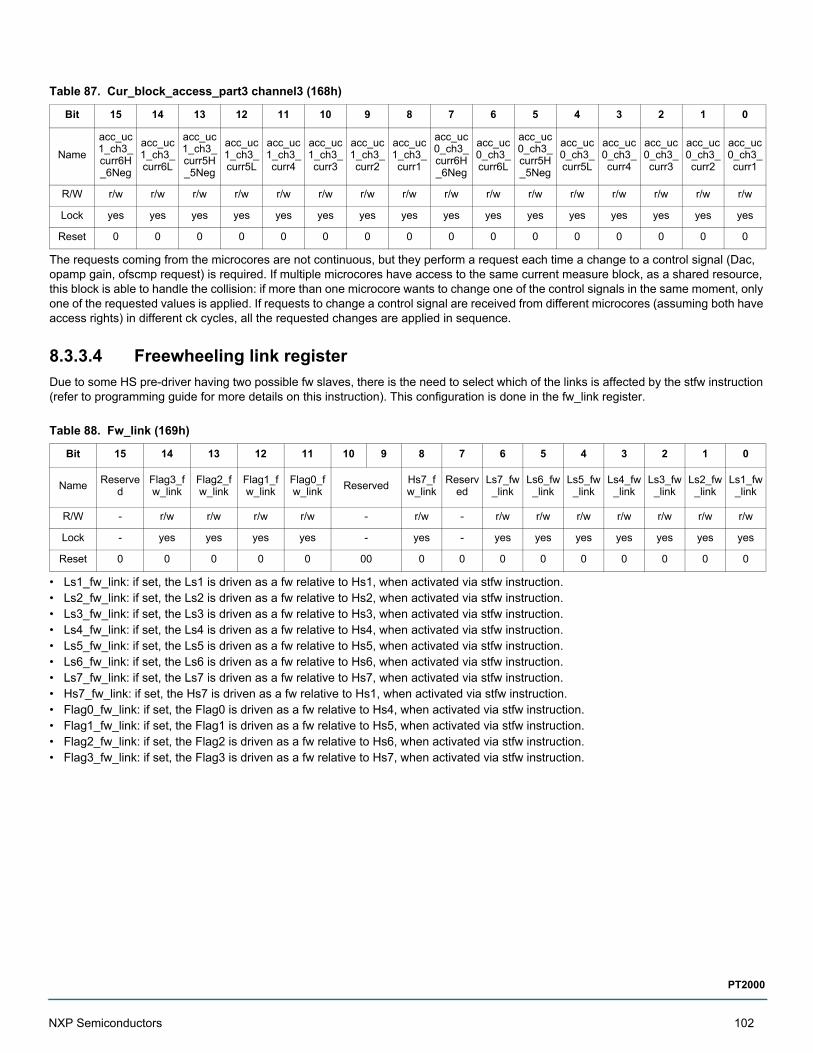
The requests coming from the microcores are not continuous, but they perform a request each time a change to a control signal (Dac, opamp gain, ofscmp request) is required. If multiple microcores have access to the same current measure block, as a shared resource, this block is able to handle the collision: if more than one microcore wants to change one of the control signals in the same moment, only one of the requested values is applied. If requests to change a control signal are received from different microcores (assuming both have access rights) in different ck cycles, all the requested changes are applied in sequence.
8.3.3.4 Freewheeling link register
Due to some HS pre-driver having two possible fw slaves, there is the need to select which of the links is affected by the stfw instruction (refer to programming guide for more details on this instruction). This configuration is done in the fw_link register.
• Ls1_fw_link: if set, the Ls1 is driven as a fw relative to Hs1, when activated via stfw instruction.• Ls2_fw_link: if set, the Ls2 is driven as a fw relative to Hs2, when activated via stfw instruction.• Ls3_fw_link: if set, the Ls3 is driven as a fw relative to Hs3, when activated via stfw instruction.• Ls4_fw_link: if set, the Ls4 is driven as a fw relative to Hs4, when activated via stfw instruction.• Ls5_fw_link: if set, the Ls5 is driven as a fw relative to Hs5, when activated via stfw instruction.• Ls6_fw_link: if set, the Ls6 is driven as a fw relative to Hs6, when activated via stfw instruction.• Ls7_fw_link: if set, the Ls7 is driven as a fw relative to Hs7, when activated via stfw instruction.• Hs7_fw_link: if set, the Hs7 is driven as a fw relative to Hs1, when activated via stfw instruction.• Flag0_fw_link: if set, the Flag0 is driven as a fw relative to Hs4, when activated via stfw instruction.• Flag1_fw_link: if set, the Flag1 is driven as a fw relative to Hs5, when activated via stfw instruction.• Flag2_fw_link: if set, the Flag2 is driven as a fw relative to Hs6, when activated via stfw instruction.• Flag3_fw_link: if set, the Flag3 is driven as a fw relative to Hs7, when activated via stfw instruction.
Table 87. Cur_block_access_part3 channel3 (168h)
Bit 15 14 13 12 11 10 9 8 7 6 5 4 3 2 1 0
Name
acc_uc1_ch3_curr6H_6Neg
acc_uc1_ch3_curr6L
acc_uc1_ch3_curr5H_5Neg
acc_uc1_ch3_curr5L
acc_uc1_ch3_curr4
acc_uc1_ch3_curr3
acc_uc1_ch3_curr2
acc_uc1_ch3_curr1
acc_uc0_ch3_curr6H_6Neg
acc_uc0_ch3_curr6L
acc_uc0_ch3_curr5H_5Neg
acc_uc0_ch3_curr5L
acc_uc0_ch3_curr4
acc_uc0_ch3_curr3
acc_uc0_ch3_curr2
acc_uc0_ch3_curr1
R/W r/w r/w r/w r/w r/w r/w r/w r/w r/w r/w r/w r/w r/w r/w r/w r/w
Lock yes yes yes yes yes yes yes yes yes yes yes yes yes yes yes yes
Reset 0 0 0 0 0 0 0 0 0 0 0 0 0 0 0 0
Table 88. Fw_link (169h)
Bit 15 14 13 12 11 10 9 8 7 6 5 4 3 2 1 0
NameReserve
dFlag3_fw_link
Flag2_fw_link
Flag1_fw_link
Flag0_fw_link
ReservedHs7_fw_link
Reserved
Ls7_fw_link
Ls6_fw_link
Ls5_fw_link
Ls4_fw_link
Ls3_fw_link
Ls2_fw_link
Ls1_fw_link
R/W - r/w r/w r/w r/w - r/w - r/w r/w r/w r/w r/w r/w r/w
Lock - yes yes yes yes - yes - yes yes yes yes yes yes yes
Reset 0 0 0 0 0 00 0 0 0 0 0 0 0 0 0
NXP Semiconductors 102
PT2000
8.3.3.5 Freewheeling external request configuration register
After the freewheeling configuration (see Table 89, Freewheeling link register) it is possible to activate automatic freewheeling by writing the corresponding bit of this register even when the microcode is not running. This can also be enabled by the stfw instruction.
• Hs1_fw_en: if set, the fw relative to Hs1 is activated, otherwise the status is defined by the microcore request (see stfw instruction).• Hs2_fw_en: if set, the fw relative to Hs2 is activated, otherwise the status is defined by the microcore request (see stfw instruction).• Hs3_fw_en: if set, the fw relative to Hs3 is activated, otherwise the status is defined by the microcore request (see stfw instruction).• Hs4_fw_en: if set, the fw relative to Hs4 is activated, otherwise the status is defined by the microcore request (see stfw instruction).• Hs5_fw_en: if set, the fw relative to Hs5 is activated, otherwise the status is defined by the microcore request (see stfw instruction).• Hs6_fw_en: if set, the fw relative to Hs6 is activated, otherwise the status is defined by the microcore request (see stfw instruction).• Hs7_fw_en: if set, the fw relative to Hs7 is activated, otherwise the status is defined by the microcore request (see stfw instruction).
Figure 32. Automatic freewheeling example
Table 89. Freewheeling link register
Freewheeling pre-driver output Related pre-driver high-side
LS1 HS1
LS2 HS2
LS3 HS3
LS4 HS4
LS5 HS5
LS6 HS6
LS7 HS7
Flag0 HS4
Flag1 HS5
Flag2 HS6
Flag3 HS7
Table 90. Fw_external_request (16ah)
Bit 15 14 13 12 11 10 9 8 7 6 5 4 3 2 1 0
Name ReservedHs7_fw_en
Hs6_fw_en
Hs5_fw_en
Hs4_fw_en
Hs3_fw_en
Hs2_fw_en
Hs1_fw_en
R/W - r/w r/w r/w r/w r/w r/w r/w
Lock - yes yes yes yes yes yes yes
Reset 000000000 0 0 0 0 0 0 0
tFWDLY tFWDLY
HS1 command
LS1 FW commandG_LS1FW
VBAT
G_HS1
103 NXP Semiconductors
PT2000

8.3.3.6 VDS and VSRC threshold selection
Each comparator threshold is expressed on 4 bits. These registers can be written through the SPI. The microcores can change the value of each field at runtime, provided they have the access right to control the related output (refer to Table 83, Out_acc_ucx_chy (160h, 161h, 162h, 163h, 164h, 165h)).
Note that when reading back this register, what is actually read from the SPI is not the content of the register, but the real configuration of the thresholds, in particular the HSx Vsrc thresholds. (see See Bootstrap switch control on page 58).
Table 91. Vds_threshold_hs_Part1 (16Bh)
Bit 15 14 13 12 11 10 9 8 7 6 5 4 3 2 1 0
Name Vds_thr_Hs4 Vds_thr_Hs3 Vds_thr_Hs2 Vds_thr_Hs1
R/W r/w r/w r/w r/w
Lock no no no no
Reset 0000 0000 0000 0000
Table 92. Vds_threshold_hs_Part2 (16Ch)
Bit 15 14 13 12 11 10 9 8 7 6 5 4 3 2 1 0
Name Reserved Vds_thr_Hs7 Vds_thr_Hs6 Vds_thr_Hs5
R/W - r/w r/w r/w
Lock - no no no
Reset 0000 0000 0000 0000
Table 93. Vsrc_threshold_hs_Part1 (16Dh)
Bit 15 14 13 12 11 10 9 8 7 6 5 4 3 2 1 0
Name Vsrc_thr_Hs4 Vsrc_thr_Hs3 Vsrc_thr_Hs2 Vsrc_thr_Hs1
R/W r/w r/w r/w r/w
Lock no no no no
Reset 0000 0000 0000 0000
Table 94. Vsrc_threshold_hs_Part2 (16Eh)
Bit 15 14 13 12 11 10 9 8 7 6 5 4 3 2 1 0
Name Reserved Vsrc_thr_Hs7 Vsrc_thr_Hs6 Vsrc_thr_Hs5
R/W - r/w r/w r/w
Lock - no no no
Reset 0000 0000 0000 0000
NXP Semiconductors 104
PT2000
Table 95. Vsrc_threshold_hs and vds_threshold_hs value
hsx_vds/src_threshold(3:0) Threshold voltage HS VDS / HS VSRC (V)
0000 0.00
1001 0.10
1010 0.20
1011 0.30
1100 0.40
0001 0.50
0010 1.0
0011 1.5
0100 2.0
0101 2.5
0110 3.0
0111 3.5
Table 96. Vds_threshold_ls_Part 1 (16Fh)
Bit 15 14 13 12 11 10 9 8 7 6 5 4 3 2 1 0
Name Vds thr Ls4 Vds thr Ls3 Vds thr Ls2 Vds thr Ls1
R/W r/w r/w r/w r/w
Lock no no no no
Reset 0000 0000 0000 0000
Table 97. Vds_threshold_ls_Part 2 (170h)
Bit 15 14 13 12 11 10 9 8 7 6 5 4 3 2 1 0
Name Vds thr Ls8 Vds thr Ls7 Vds thr Ls6 Vds thr Ls5
R/W r/w r/w r/w r/w
Lock no no no no
Reset 0000 0000 0000 0000
105 NXP Semiconductors
PT2000
8.3.3.7 Slew rate high-side and low-side selection register
These registers store the slew rate configuration value for each output driver. The microcores can change the value of each field at runtime, provided they have the access right to control the related output (refer to Table 83, Out_acc_ucx_chy (160h, 161h, 162h, 163h, 164h, 165h)). Each output has the same slew rate for the rising and falling edge, save for the low-side 7 and 8.
Refer to Table 22 for the slew rates values.
Refer to Table 25 for slew rates values.
Table 98. Vds_threshold_ls value
lsx_vds _threshold(3:0) Threshold Voltage LS VDS (V)
0000 0.00
1001 0.10
1010 0.20
1011 0.30
1100 0.40
0001 0.50
0010 1.0
0011 1.5
0100 2.0
0101 2.5
0110 3.0
0111 3.5
Table 99. Hs_slewrate (171h)
Bit 15 14 13 12 11 10 9 8 7 6 5 4 3 2 1 0
Name Reserved slewrate_hs7 slewrate_hs6 slewrate_hs5 slewrate_hs4 slewrate_hs3 slewrate_hs2 slewrate_hs1
R/W - r/w r/w r/w r/w r/w r/w r/w
Lock - no no no no no no no
Reset 00 00 00 00 00 00 00 00
Table 100. Ls_slewrate_Part 1 (172h)
Bit 15 14 13 12 11 10 9 8 7 6 5 4 3 2 1 0
Name Reserved slewrate_ls6 slewrate_ls5 slewrate_ls4 slewrate_ls3 slewrate_ls2 slewrate_ls1
R/W - r/w r/w r/w r/w r/w r/w
Lock - no no no no no no
Reset 0000 00 00 00 00 00 00
NXP Semiconductors 106
PT2000
Refer to Table 28 and Table 29 for slew rates values.
8.3.3.8 Offset compensation results registers
It is possible to measure the offset of each current measure block, including opamp, DAC and comparator; for current measure block 5 and 6, only comparator 5L and 6L, the relative opamp, and the DAC 5L and 6L are considered. The measured offset is automatically compensated during normal operation. The compensation must be enabled by the microcores (when the input current to the current measurement block is 0) with the “stoc” instruction (refer to programming user guide).
The offset can be read through the SPI registers. It is also possible to change the value compensated by writing these registers. If the offset compensation is requested by microcores, it starts from the precedent result (or from the data forced through the SPI). As the offset can be both positive and negative, all the values in these registers are represented as two’s complement.
The offset values are stored in registers using the two’s complement notation. The values can range from -32 to 31. The value is then converted to sign-module notation before being transferred to the analog section.
Table 101. Ls_slewrate_Part 2 (173h)
Bit 15 14 13 12 11 10 9 8 7 6 5 4 3 2 1 0
Name Reservedslewrate_LS8_ri
singslewrate_LS8_fa
llingslewrate_LS7_ri
singslewrate_LS7_f
alling
R/W - r/w r/w r/w r/w
Lock - no no no no
Reset 00000000 00 00 00 00
Table 102. Offset_compensation12 (174h)
Bit 15 14 13 12 11 10 9 8 7 6 5 4 3 2 1 0
Name Reserved Offset_current_measure_block_2 Reserved Offset_current_measure_block_1
R/W - r/w - r/w
Lock - no - no
Reset 00 000000 00 000000
Table 103. Offset_compensation34 (175h)
Bit 15 14 13 12 11 10 9 8 7 6 5 4 3 2 1 0
Name Reserved Offset_current_measure_block_4 Reserved Offset_current_measure_block_3
R/W - r/w - r/w
Lock - no - no
Reset 00 000000 00 000000
Table 104. Offset_compensation56 (176h)
Bit 15 14 13 12 11 10 9 8 7 6 5 4 3 2 1 0
Name Reserved Offset_current_measure_block_6 Reserved Offset_current_measure_block_5
R/W - r/w - r/w
Lock - no - no
Reset 00 000000 00 000000
107 NXP Semiconductors
PT2000
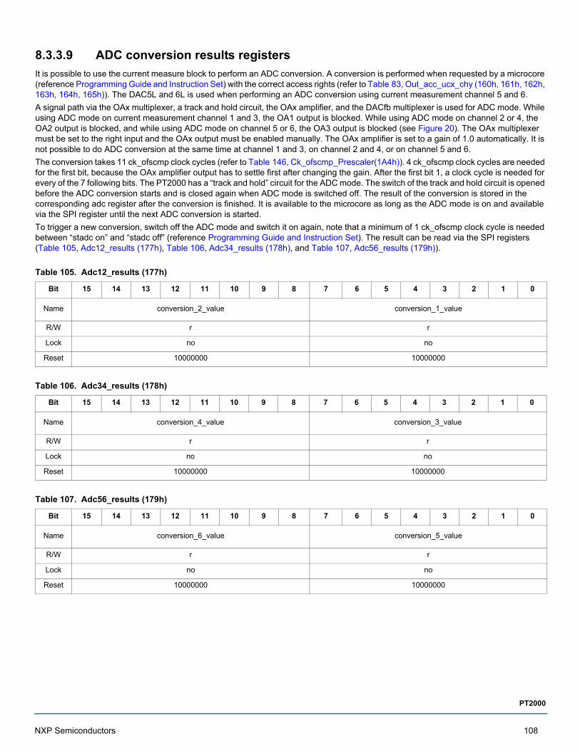
8.3.3.9 ADC conversion results registers
It is possible to use the current measure block to perform an ADC conversion. A conversion is performed when requested by a microcore (reference Programming Guide and Instruction Set) with the correct access rights (refer to Table 83, Out_acc_ucx_chy (160h, 161h, 162h, 163h, 164h, 165h)). The DAC5L and 6L is used when performing an ADC conversion using current measurement channel 5 and 6.
A signal path via the OAx multiplexer, a track and hold circuit, the OAx amplifier, and the DACfb multiplexer is used for ADC mode. While using ADC mode on current measurement channel 1 and 3, the OA1 output is blocked. While using ADC mode on channel 2 or 4, the OA2 output is blocked, and while using ADC mode on channel 5 or 6, the OA3 output is blocked (see Figure 20). The OAx multiplexer must be set to the right input and the OAx output must be enabled manually. The OAx amplifier is set to a gain of 1.0 automatically. It is not possible to do ADC conversion at the same time at channel 1 and 3, on channel 2 and 4, or on channel 5 and 6.
The conversion takes 11 ck_ofscmp clock cycles (refer to Table 146, Ck_ofscmp_Prescaler(1A4h)). 4 ck_ofscmp clock cycles are needed for the first bit, because the OAx amplifier output has to settle first after changing the gain. After the first bit 1, a clock cycle is needed for every of the 7 following bits. The PT2000 has a “track and hold” circuit for the ADC mode. The switch of the track and hold circuit is opened before the ADC conversion starts and is closed again when ADC mode is switched off. The result of the conversion is stored in the corresponding adc register after the conversion is finished. It is available to the microcore as long as the ADC mode is on and available via the SPI register until the next ADC conversion is started.
To trigger a new conversion, switch off the ADC mode and switch it on again, note that a minimum of 1 ck_ofscmp clock cycle is needed between “stadc on” and “stadc off” (reference Programming Guide and Instruction Set). The result can be read via the SPI registers (Table 105, Adc12_results (177h), Table 106, Adc34_results (178h), and Table 107, Adc56_results (179h)).
Table 105. Adc12_results (177h)
Bit 15 14 13 12 11 10 9 8 7 6 5 4 3 2 1 0
Name conversion_2_value conversion_1_value
R/W r r
Lock no no
Reset 10000000 10000000
Table 106. Adc34_results (178h)
Bit 15 14 13 12 11 10 9 8 7 6 5 4 3 2 1 0
Name conversion_4_value conversion_3_value
R/W r r
Lock no no
Reset 10000000 10000000
Table 107. Adc56_results (179h)
Bit 15 14 13 12 11 10 9 8 7 6 5 4 3 2 1 0
Name conversion_6_value conversion_5_value
R/W r r
Lock no no
Reset 10000000 10000000
NXP Semiconductors 108
PT2000
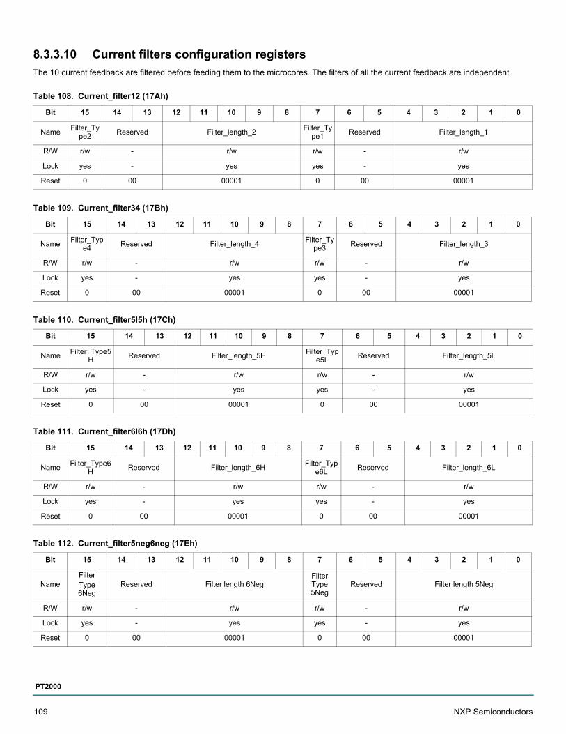
8.3.3.10 Current filters configuration registers
The 10 current feedback are filtered before feeding them to the microcores. The filters of all the current feedback are independent.
Table 108. Current_filter12 (17Ah)
Bit 15 14 13 12 11 10 9 8 7 6 5 4 3 2 1 0
NameFilter_Ty
pe2Reserved Filter_length_2
Filter_Type1
Reserved Filter_length_1
R/W r/w - r/w r/w - r/w
Lock yes - yes yes - yes
Reset 0 00 00001 0 00 00001
Table 109. Current_filter34 (17Bh)
Bit 15 14 13 12 11 10 9 8 7 6 5 4 3 2 1 0
NameFilter_Typ
e4Reserved Filter_length_4
Filter_Type3
Reserved Filter_length_3
R/W r/w - r/w r/w - r/w
Lock yes - yes yes - yes
Reset 0 00 00001 0 00 00001
Table 110. Current_filter5l5h (17Ch)
Bit 15 14 13 12 11 10 9 8 7 6 5 4 3 2 1 0
NameFilter_Type5
HReserved Filter_length_5H
Filter_Type5L
Reserved Filter_length_5L
R/W r/w - r/w r/w - r/w
Lock yes - yes yes - yes
Reset 0 00 00001 0 00 00001
Table 111. Current_filter6l6h (17Dh)
Bit 15 14 13 12 11 10 9 8 7 6 5 4 3 2 1 0
NameFilter_Type6
HReserved Filter_length_6H
Filter_Type6L
Reserved Filter_length_6L
R/W r/w - r/w r/w - r/w
Lock yes - yes yes - yes
Reset 0 00 00001 0 00 00001
Table 112. Current_filter5neg6neg (17Eh)
Bit 15 14 13 12 11 10 9 8 7 6 5 4 3 2 1 0
NameFilterType 6Neg
Reserved Filter length 6NegFilter Type 5Neg
Reserved Filter length 5Neg
R/W r/w - r/w r/w - r/w
Lock yes - yes yes - yes
Reset 0 00 00001 0 00 00001
109 NXP Semiconductors
PT2000
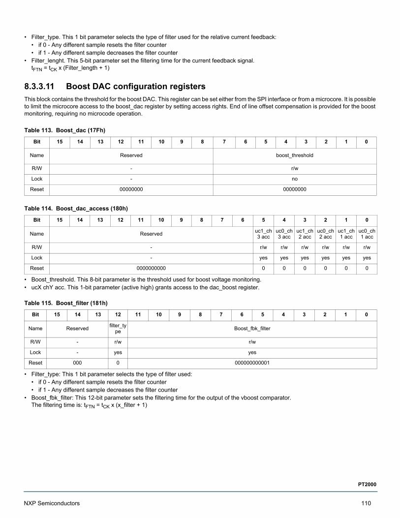
• Filter_type. This 1 bit parameter selects the type of filter used for the relative current feedback:• if 0 - Any different sample resets the filter counter• if 1 - Any different sample decreases the filter counter
• Filter_lenght. This 5-bit parameter set the filtering time for the current feedback signal. tFTN = tCK x (Filter_length + 1)
8.3.3.11 Boost DAC configuration registers
This block contains the threshold for the boost DAC. This register can be set either from the SPI interface or from a microcore. It is possible to limit the microcore access to the boost_dac register by setting access rights. End of line offset compensation is provided for the boost monitoring, requiring no microcode operation.
• Boost_threshold. This 8-bit parameter is the threshold used for boost voltage monitoring.• ucX chY acc. This 1-bit parameter (active high) grants access to the dac_boost register.
• Filter_type: This 1 bit parameter selects the type of filter used:• if 0 - Any different sample resets the filter counter• if 1 - Any different sample decreases the filter counter
• Boost_fbk_filter: This 12-bit parameter sets the filtering time for the output of the vboost comparator. The filtering time is: tFTN = tCK x (x_filter + 1)
Table 113. Boost_dac (17Fh)
Bit 15 14 13 12 11 10 9 8 7 6 5 4 3 2 1 0
Name Reserved boost_threshold
R/W - r/w
Lock - no
Reset 00000000 00000000
Table 114. Boost_dac_access (180h)
Bit 15 14 13 12 11 10 9 8 7 6 5 4 3 2 1 0
Name Reserveduc1_ch3 acc
uc0_ch3 acc
uc1_ch2 acc
uc0_ch2 acc
uc1_ch1 acc
uc0_ch1 acc
R/W - r/w r/w r/w r/w r/w r/w
Lock - yes yes yes yes yes yes
Reset 0000000000 0 0 0 0 0 0
Table 115. Boost_filter (181h)
Bit 15 14 13 12 11 10 9 8 7 6 5 4 3 2 1 0
Name Reservedfilter_ty
peBoost_fbk_filter
R/W - r/w r/w
Lock - yes yes
Reset 000 0 000000000001
NXP Semiconductors 110
PT2000

8.3.3.12 VDS low-side 7/8 configuration register
These two registers are used for configuring the timeout for VDS monitoring of DC/DC resonant converter. If VBOOST drops below 2 x VBAT, VDS would not fall below the VDS threshold of 2.5 V, which would not activate the MOSFET in resonant DC/DC converter mode again. Therefore this timeout is required to force the MOSFET to be switched on. The access for this register is only via the SPI.
• Vdsx_dcdc timeout: This 8 bit parameter defines the time duration of the DC/DC converter (VDS7/8 monitoring Ls7/8). It is needed only if the async_vds mode is used. Timeout is used if the VDS threshold 2.5 V is not reached.• The timeout is: tFTN = tCK x (x_filter + 1)
• Vdsx_to_en: VDS7/8 timeout is enabled. MOSFET is activated automatically when the timeout has been exceeded• Cur_dcdcx_fbk_sel for async_vds and sync mode:
• For LS7:• 0: selects cur5h_dcdc feedback signal• 1: selects cur6h_dcdc feedback signal
• For LS8:• 0: selects cur6h_dcdc feedback signal• 1: selects cur5h_dcdc feedback signal
• Lsx_vds_highspeed_en: Enable high speed VDS comparator for DC/DC control• 0: standard low speed VDS monitor enabled• 1: high speed VDS monitor for DC/DC control enabled
• dcdcx_mode. This bits shows when the automatic DC/DC control feature for LS7/8 is enabled. Refer to See DC/DC converter control (LS7/8) on page 61 for the behavior of LS7/8 during this mode.
8.3.3.13 Battery monitoring results
This block contains the result of the batt DAC plus comparator in ADC mode. This register can be read either from the SPI interface or from a microcore.
The ofs_comp_prescaler is used to define the step length of the ADC conversion. The ADC mode is running continuously. One conversion needs 7 cycles.
Table 116. Vds7_dcdc_config (182h) & Vds8_dcdc_config (183h)
Bit 15 14 13 12 11 10 9 8 7 6 5 4 3 2 1 0
Name dcdcx mode Reservedlsx_vds_highspeed_en
Cur_dcdcx_fbk_sel
vdsx_ to_en
vdsx_dcdc_timeout
R/W r - r/w r/w r/w r/w
Lock - - no no no no
Reset 00 000 0 0 0 00000000
Table 117. DC/DC mode
DC/DC Mode Description
00, 10 Sync mode enabled. LS7/8 controlled by microcore command
01 Async mode enabled with two current thresholds.
11 Async mode enabled with one current threshold and VDS monitor.
Table 118. batt_results (184h)
Bit 15 14 13 12 11 10 9 8 7 6 5 4 3 2 1 0
Name Reserved batt_result
R/W - r/w
Lock - no
Reset 00000000 000000
111 NXP Semiconductors
PT2000
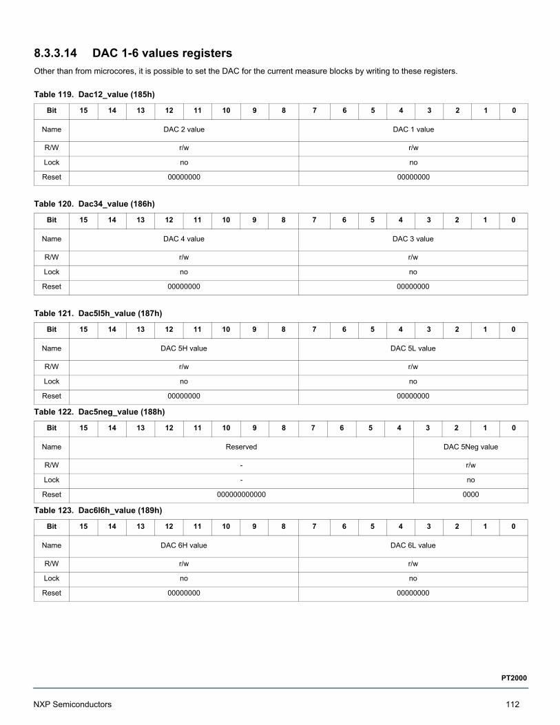
8.3.3.14 DAC 1-6 values registers
Other than from microcores, it is possible to set the DAC for the current measure blocks by writing to these registers.
Table 119. Dac12_value (185h)
Bit 15 14 13 12 11 10 9 8 7 6 5 4 3 2 1 0
Name DAC 2 value DAC 1 value
R/W r/w r/w
Lock no no
Reset 00000000 00000000
Table 120. Dac34_value (186h)
Bit 15 14 13 12 11 10 9 8 7 6 5 4 3 2 1 0
Name DAC 4 value DAC 3 value
R/W r/w r/w
Lock no no
Reset 00000000 00000000
Table 121. Dac5l5h_value (187h)
Bit 15 14 13 12 11 10 9 8 7 6 5 4 3 2 1 0
Name DAC 5H value DAC 5L value
R/W r/w r/w
Lock no no
Reset 00000000 00000000
Table 122. Dac5neg_value (188h)
Bit 15 14 13 12 11 10 9 8 7 6 5 4 3 2 1 0
Name Reserved DAC 5Neg value
R/W - r/w
Lock - no
Reset 000000000000 0000
Table 123. Dac6l6h_value (189h)
Bit 15 14 13 12 11 10 9 8 7 6 5 4 3 2 1 0
Name DAC 6H value DAC 6L value
R/W r/w r/w
Lock no no
Reset 00000000 00000000
NXP Semiconductors 112
PT2000
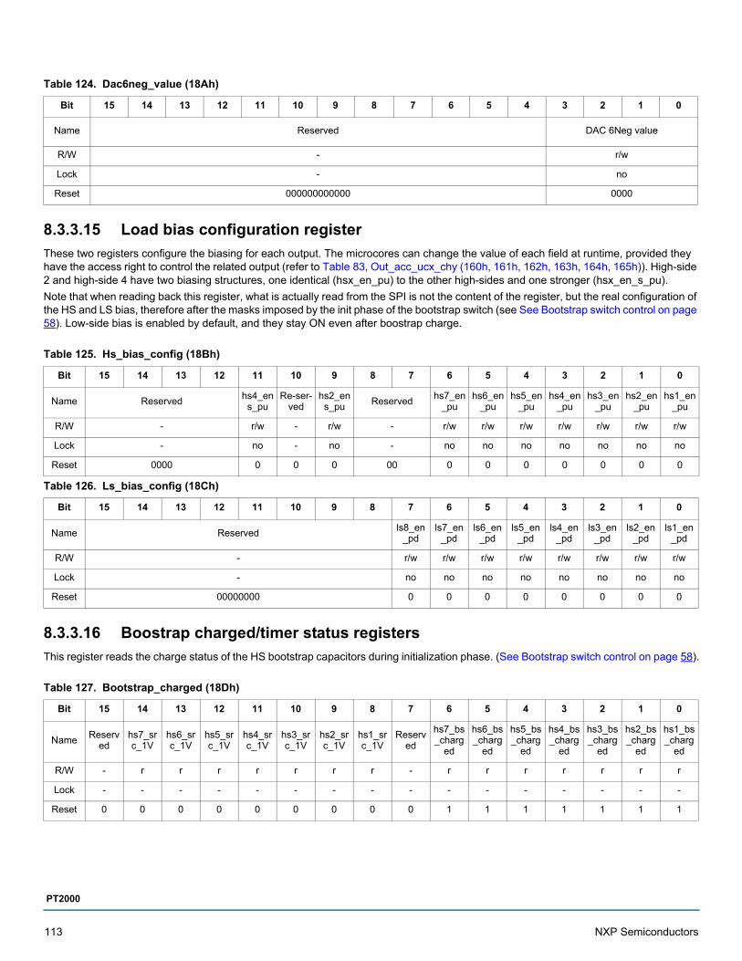
8.3.3.15 Load bias configuration register
These two registers configure the biasing for each output. The microcores can change the value of each field at runtime, provided they have the access right to control the related output (refer to Table 83, Out_acc_ucx_chy (160h, 161h, 162h, 163h, 164h, 165h)). High-side 2 and high-side 4 have two biasing structures, one identical (hsx_en_pu) to the other high-sides and one stronger (hsx_en_s_pu).
Note that when reading back this register, what is actually read from the SPI is not the content of the register, but the real configuration of the HS and LS bias, therefore after the masks imposed by the init phase of the bootstrap switch (see See Bootstrap switch control on page 58). Low-side bias is enabled by default, and they stay ON even after boostrap charge.
8.3.3.16 Boostrap charged/timer status registers
This register reads the charge status of the HS bootstrap capacitors during initialization phase. (See Bootstrap switch control on page 58).
Table 124. Dac6neg_value (18Ah)
Bit 15 14 13 12 11 10 9 8 7 6 5 4 3 2 1 0
Name Reserved DAC 6Neg value
R/W - r/w
Lock - no
Reset 000000000000 0000
Table 125. Hs_bias_config (18Bh)
Bit 15 14 13 12 11 10 9 8 7 6 5 4 3 2 1 0
Name Reservedhs4_en s_pu
Re-ser-ved
hs2_en s_pu
Reservedhs7_en
_puhs6_en
_puhs5_en
_puhs4_en
_puhs3_en
_puhs2_en
_puhs1_en
_pu
R/W - r/w - r/w - r/w r/w r/w r/w r/w r/w r/w
Lock - no - no - no no no no no no no
Reset 0000 0 0 0 00 0 0 0 0 0 0 0
Table 126. Ls_bias_config (18Ch)
Bit 15 14 13 12 11 10 9 8 7 6 5 4 3 2 1 0
Name Reservedls8_en
_pdls7_en
_pdls6_en
_pdls5_en
_pdls4_en
_pdls3_en
_pdls2_en
_pdls1_en
_pd
R/W - r/w r/w r/w r/w r/w r/w r/w r/w
Lock - no no no no no no no no
Reset 00000000 0 0 0 0 0 0 0 0
Table 127. Bootstrap_charged (18Dh)
Bit 15 14 13 12 11 10 9 8 7 6 5 4 3 2 1 0
NameReserv
edhs7_src_1V
hs6_src_1V
hs5_src_1V
hs4_src_1V
hs3_src_1V
hs2_src_1V
hs1_src_1V
Reserved
hs7_bs_charg
ed
hs6_bs_charg
ed
hs5_bs_charg
ed
hs4_bs_charg
ed
hs3_bs_charg
ed
hs2_bs_charg
ed
hs1_bs_charg
ed
R/W - r r r r r r r - r r r r r r r
Lock - - - - - - - - - - - - - - - -
Reset 0 0 0 0 0 0 0 0 0 1 1 1 1 1 1 1
113 NXP Semiconductors
PT2000

• hsx_bs_charged: when '0', the bootstrap capacitor for HSx is charged• hsx_src_1V: when '1' it was necessary for this pre-driver to switch the VSRC threshold to 1.0 V to finish the bootstrap init• bootstrap init timer: this shows the current value of the six MSBs of the bootstrap init timer. The value is '110100' when the timer expires
Table 129, Bootstrap_charged Bits shows the exact meaning of the bits hsx_bs_charged and hsx_src_1V.
The bootstrap init timer value can be used, together with the other bits of the register, to identify in detail how much time has passed since VCCP voltage was stable and which threshold is used to detect the charge of the bootstrap capacitor.
Table 128. Bootstrap_timer (18Eh)
Bit 15 14 13 12 11 10 9 8 7 6 5 4 3 2 1 0
Name bootstrap_init_timer Reserved
R/W r -
Lock - -
Reset 000000 0000000000
Table 129. Bootstrap_charged Bits
hsx_bs_charged hsx_src_1V Description
1 0 Bootstrap capacitor not charged, bootstrap init timer not lapsed, VSRC = 0.5 V (reset value)
1 1 Bootstrap capacitor not charged, timer lapsed, VSRC = 1.0 V
0 0 Bootstrap capacitor charged, VSRC = 0.5 V when charging finished
0 1 Bootstrap capacitor charged, VSRC = 1.0 V when charging finished
Table 130. Bootstrap init timer
Bit value Description
000000 VCCP voltage is not stable (undervoltage)
000001 VCCP voltage is stable since 0.68 ms (214 / 24 MHz). Source HS voltage threshold used to detect bootstrap charge is 0.5 V
… …
100000 VCCP voltage is stable since 21.8 ms. Source HS voltage threshold used to detect bootstrap charge is 0.5 V
… …
110011 VCCP voltage is stable since 34.8 ms. Source HS voltage threshold used to detect bootstrap charge is 0.5 V
110100 (final value) VCCP voltage is stable since at least 35.5 ms. Source HS voltage threshold used to detect bootstrap charge is 1.0 V.
NXP Semiconductors 114
PT2000
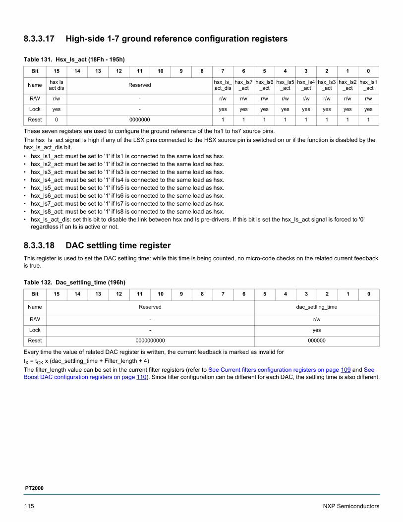
8.3.3.17 High-side 1-7 ground reference configuration registers
These seven registers are used to configure the ground reference of the hs1 to hs7 source pins.
The hsx_ls_act signal is high if any of the LSX pins connected to the HSX source pin is switched on or if the function is disabled by the hsx_ls_act_dis bit.
• hsx_ls1_act: must be set to '1' if ls1 is connected to the same load as hsx.• hsx_ls2_act: must be set to '1' if ls2 is connected to the same load as hsx.• hsx_ls3_act: must be set to '1' if ls3 is connected to the same load as hsx.• hsx_ls4_act: must be set to '1' if ls4 is connected to the same load as hsx.• hsx_ls5_act: must be set to '1' if ls5 is connected to the same load as hsx.• hsx_ls6_act: must be set to '1' if ls6 is connected to the same load as hsx.• hsx_ls7_act: must be set to '1' if ls7 is connected to the same load as hsx.• hsx_ls8_act: must be set to '1' if ls8 is connected to the same load as hsx.• hsx_ls_act_dis: set this bit to disable the link between hsx and ls pre-drivers. If this bit is set the hsx_ls_act signal is forced to '0'
regardless if an ls is active or not.
8.3.3.18 DAC settling time register
This register is used to set the DAC settling time: while this time is being counted, no micro-code checks on the related current feedback is true.
Every time the value of related DAC register is written, the current feedback is marked as invalid for
tX = tCK x (dac_settling_time + Filter_length + 4)
The filter_length value can be set in the current filter registers (refer to See Current filters configuration registers on page 109 and See Boost DAC configuration registers on page 110). Since filter configuration can be different for each DAC, the settling time is also different.
Table 131. Hsx_ls_act (18Fh - 195h)
Bit 15 14 13 12 11 10 9 8 7 6 5 4 3 2 1 0
Namehsx ls act dis
Reservedhsx_ls_act_dis
hsx_ls7_act
hsx_ls6_act
hsx_ls5_act
hsx_ls4_act
hsx_ls3_act
hsx_ls2_act
hsx_ls1_act
R/W r/w - r/w r/w r/w r/w r/w r/w r/w r/w
Lock yes - yes yes yes yes yes yes yes yes
Reset 0 0000000 1 1 1 1 1 1 1 1
Table 132. Dac_settling_time (196h)
Bit 15 14 13 12 11 10 9 8 7 6 5 4 3 2 1 0
Name Reserved dac_settling_time
R/W - r/w
Lock - yes
Reset 0000000000 000000
115 NXP Semiconductors
PT2000
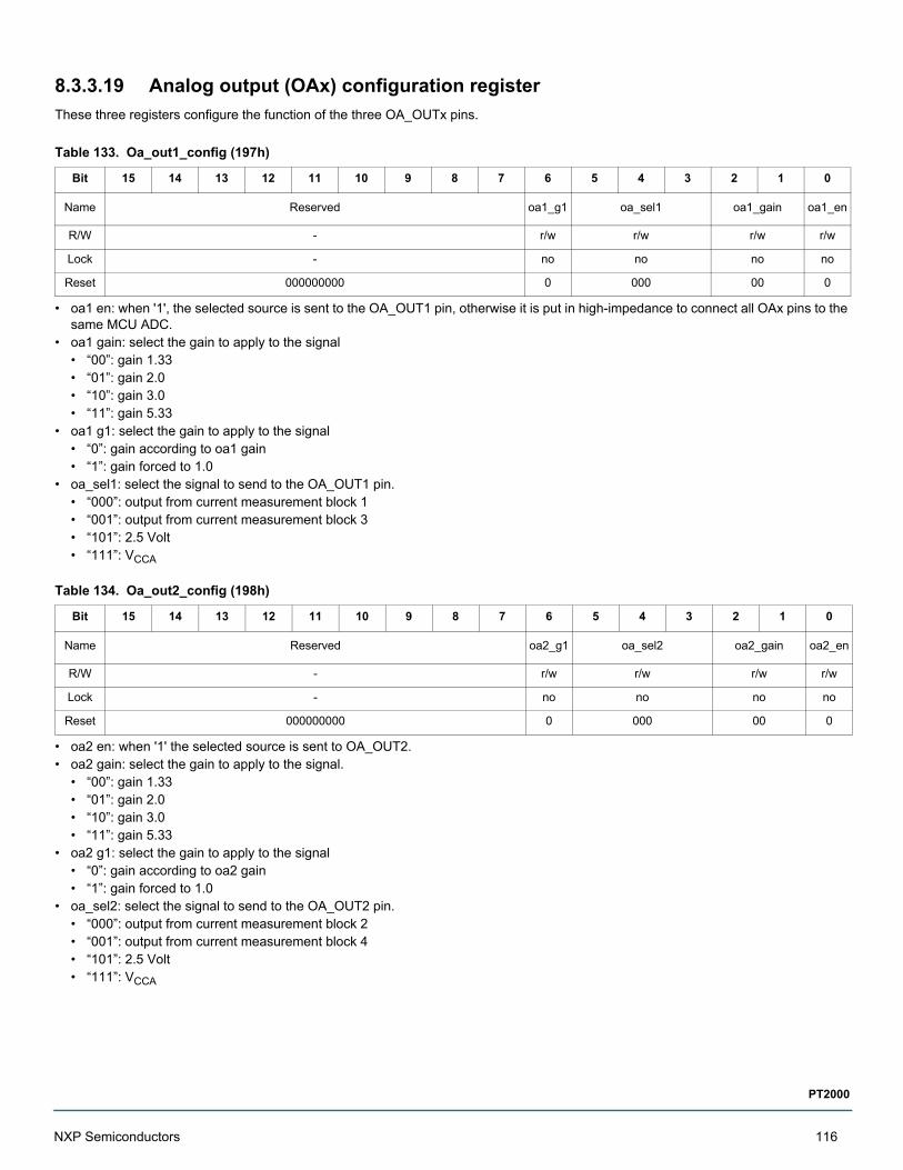
8.3.3.19 Analog output (OAx) configuration register
These three registers configure the function of the three OA_OUTx pins.
• oa1 en: when '1', the selected source is sent to the OA_OUT1 pin, otherwise it is put in high-impedance to connect all OAx pins to the same MCU ADC.
• oa1 gain: select the gain to apply to the signal• “00”: gain 1.33• “01”: gain 2.0• “10”: gain 3.0• “11”: gain 5.33
• oa1 g1: select the gain to apply to the signal• “0”: gain according to oa1 gain• “1”: gain forced to 1.0
• oa_sel1: select the signal to send to the OA_OUT1 pin.• “000”: output from current measurement block 1• “001”: output from current measurement block 3• “101”: 2.5 Volt• “111”: VCCA
• oa2 en: when '1' the selected source is sent to OA_OUT2.• oa2 gain: select the gain to apply to the signal.
• “00”: gain 1.33• “01”: gain 2.0• “10”: gain 3.0• “11”: gain 5.33
• oa2 g1: select the gain to apply to the signal• “0”: gain according to oa2 gain• “1”: gain forced to 1.0
• oa_sel2: select the signal to send to the OA_OUT2 pin.• “000”: output from current measurement block 2• “001”: output from current measurement block 4• “101”: 2.5 Volt• “111”: VCCA
Table 133. Oa_out1_config (197h)
Bit 15 14 13 12 11 10 9 8 7 6 5 4 3 2 1 0
Name Reserved oa1_g1 oa_sel1 oa1_gain oa1_en
R/W - r/w r/w r/w r/w
Lock - no no no no
Reset 000000000 0 000 00 0
Table 134. Oa_out2_config (198h)
Bit 15 14 13 12 11 10 9 8 7 6 5 4 3 2 1 0
Name Reserved oa2_g1 oa_sel2 oa2_gain oa2_en
R/W - r/w r/w r/w r/w
Lock - no no no no
Reset 000000000 0 000 00 0
NXP Semiconductors 116
PT2000
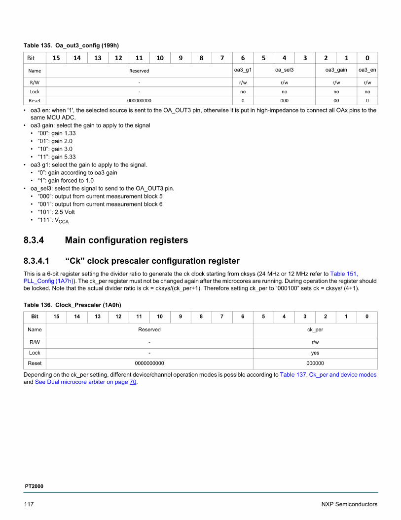
• oa3 en: when '1', the selected source is sent to the OA_OUT3 pin, otherwise it is put in high-impedance to connect all OAx pins to the same MCU ADC.
• oa3 gain: select the gain to apply to the signal• “00”: gain 1.33• “01”: gain 2.0• “10”: gain 3.0• “11”: gain 5.33
• oa3 g1: select the gain to apply to the signal.• “0”: gain according to oa3 gain• “1”: gain forced to 1.0
• oa_sel3: select the signal to send to the OA_OUT3 pin.• “000”: output from current measurement block 5• “001”: output from current measurement block 6• “101”: 2.5 Volt• “111”: VCCA
8.3.4 Main configuration registers
8.3.4.1 “Ck” clock prescaler configuration register
This is a 6-bit register setting the divider ratio to generate the ck clock starting from cksys (24 MHz or 12 MHz refer to Table 151, PLL_Config (1A7h)). The ck_per register must not be changed again after the microcores are running. During operation the register should be locked. Note that the actual divider ratio is ck = cksys/(ck_per+1). Therefore setting ck_per to “000100” sets ck = cksys/ (4+1).
Depending on the ck_per setting, different device/channel operation modes is possible according to Table 137, Ck_per and device modes and See Dual microcore arbiter on page 70.
Table 135. Oa_out3_config (199h)
Bit 15 14 13 12 11 10 9 8 7 6 5 4 3 2 1 0
Name Reserved oa3_g1 oa_sel3 oa3_gain oa3_en
R/W - r/w r/w r/w r/w
Lock - no no no no
Reset 000000000 0 000 00 0
Table 136. Clock_Prescaler (1A0h)
Bit 15 14 13 12 11 10 9 8 7 6 5 4 3 2 1 0
Name Reserved ck_per
R/W - r/w
Lock - yes
Reset 0000000000 000000
117 NXP Semiconductors
PT2000
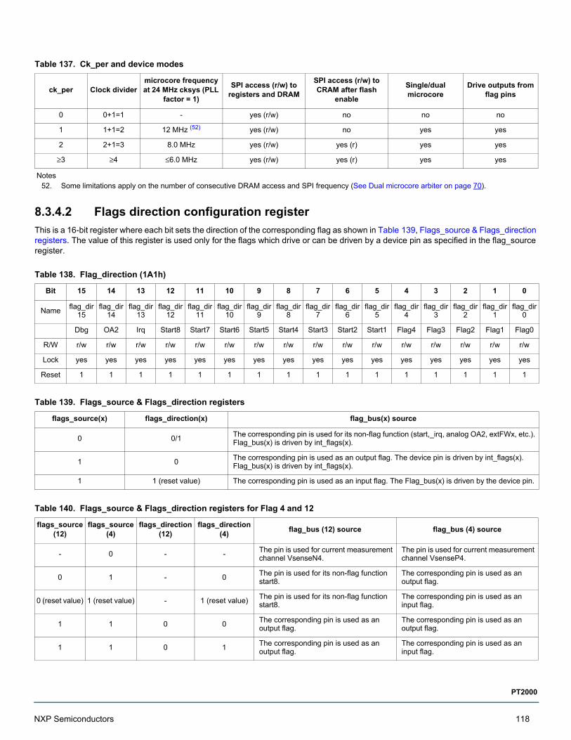
8.3.4.2 Flags direction configuration register
This is a 16-bit register where each bit sets the direction of the corresponding flag as shown in Table 139, Flags_source & Flags_direction registers. The value of this register is used only for the flags which drive or can be driven by a device pin as specified in the flag_source register.
Table 137. Ck_per and device modes
ck_per Clock dividermicrocore frequency at 24 MHz cksys (PLL
factor = 1)
SPI access (r/w) to registers and DRAM
SPI access (r/w) to CRAM after flash
enable
Single/dual microcore
Drive outputs from flag pins
0 0+1=1 - yes (r/w) no no no
1 1+1=2 12 MHz (52) yes (r/w) no yes yes
2 2+1=3 8.0 MHz yes (r/w) yes (r) yes yes
≥3 ≥4 ≤6.0 MHz yes (r/w) yes (r) yes yes
Notes52. Some limitations apply on the number of consecutive DRAM access and SPI frequency (See Dual microcore arbiter on page 70).
Table 138. Flag_direction (1A1h)
Bit 15 14 13 12 11 10 9 8 7 6 5 4 3 2 1 0
Nameflag_dir
15flag_dir
14flag_dir
13flag_dir
12flag_dir
11flag_dir
10flag_dir
9flag_dir
8flag_dir
7flag_dir
6flag_dir
5flag_dir
4flag_dir
3flag_dir
2flag_dir
1flag_dir
0
Dbg OA2 Irq Start8 Start7 Start6 Start5 Start4 Start3 Start2 Start1 Flag4 Flag3 Flag2 Flag1 Flag0
R/W r/w r/w r/w r/w r/w r/w r/w r/w r/w r/w r/w r/w r/w r/w r/w r/w
Lock yes yes yes yes yes yes yes yes yes yes yes yes yes yes yes yes
Reset 1 1 1 1 1 1 1 1 1 1 1 1 1 1 1 1
Table 139. Flags_source & Flags_direction registers
flags_source(x) flags_direction(x) flag_bus(x) source
0 0/1The corresponding pin is used for its non-flag function (start,_irq, analog OA2, extFWx, etc.). Flag_bus(x) is driven by int_flags(x).
1 0The corresponding pin is used as an output flag. The device pin is driven by int_flags(x). Flag_bus(x) is driven by int_flags(x).
1 1 (reset value) The corresponding pin is used as an input flag. The Flag_bus(x) is driven by the device pin.
Table 140. Flags_source & Flags_direction registers for Flag 4 and 12
flags_source (12)
flags_source (4)
flags_direction (12)
flags_direction (4)
flag_bus (12) source flag_bus (4) source
- 0 - -The pin is used for current measurement channel VsenseN4.
The pin is used for current measurement channel VsenseP4.
0 1 - 0The pin is used for its non-flag function start8.
The corresponding pin is used as an output flag.
0 (reset value) 1 (reset value) - 1 (reset value)The pin is used for its non-flag function start8.
The corresponding pin is used as an input flag.
1 1 0 0The corresponding pin is used as an output flag.
The corresponding pin is used as an output flag.
1 1 0 1The corresponding pin is used as an output flag.
The corresponding pin is used as an input flag.
NXP Semiconductors 118
PT2000
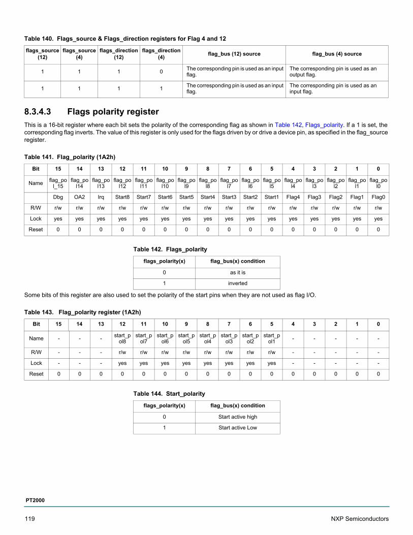
8.3.4.3 Flags polarity register
This is a 16-bit register where each bit sets the polarity of the corresponding flag as shown in Table 142, Flags_polarity. If a 1 is set, the corresponding flag inverts. The value of this register is only used for the flags driven by or drive a device pin, as specified in the flag_source register.
Some bits of this register are also used to set the polarity of the start pins when they are not used as flag I/O.
1 1 1 0The corresponding pin is used as an input flag.
The corresponding pin is used as an output flag.
1 1 1 1The corresponding pin is used as an input flag.
The corresponding pin is used as an input flag.
Table 141. Flag_polarity (1A2h)
Bit 15 14 13 12 11 10 9 8 7 6 5 4 3 2 1 0
Nameflag_po
l_15flag_po
l14flag_po
l13flag_po
l12flag_po
l11flag_po
l10flag_po
l9flag_po
l8flag_po
l7flag_po
l6flag_po
l5flag_po
l4flag_po
l3flag_po
l2flag_po
l1flag_po
l0
Dbg OA2 Irq Start8 Start7 Start6 Start5 Start4 Start3 Start2 Start1 Flag4 Flag3 Flag2 Flag1 Flag0
R/W r/w r/w r/w r/w r/w r/w r/w r/w r/w r/w r/w r/w r/w r/w r/w r/w
Lock yes yes yes yes yes yes yes yes yes yes yes yes yes yes yes yes
Reset 0 0 0 0 0 0 0 0 0 0 0 0 0 0 0 0
Table 142. Flags_polarity
flags_polarity(x) flag_bus(x) condition
0 as it is
1 inverted
Table 143. Flag_polarity register (1A2h)
Bit 15 14 13 12 11 10 9 8 7 6 5 4 3 2 1 0
Name - - -start_p
ol8start_p
ol7start_p
ol6start_p
ol5start_p
ol4start_p
ol3start_p
ol2start_p
ol1- - - - -
R/W - - - r/w r/w r/w r/w r/w r/w r/w r/w - - - - -
Lock - - - yes yes yes yes yes yes yes yes - - - - -
Reset 0 0 0 0 0 0 0 0 0 0 0 0 0 0 0 0
Table 144. Start_polarity
flags_polarity(x) flag_bus(x) condition
0 Start active high
1 Start active Low
Table 140. Flags_source & Flags_direction registers for Flag 4 and 12
flags_source (12)
flags_source (4)
flags_direction (12)
flags_direction (4)
flag_bus (12) source flag_bus (4) source
119 NXP Semiconductors
PT2000
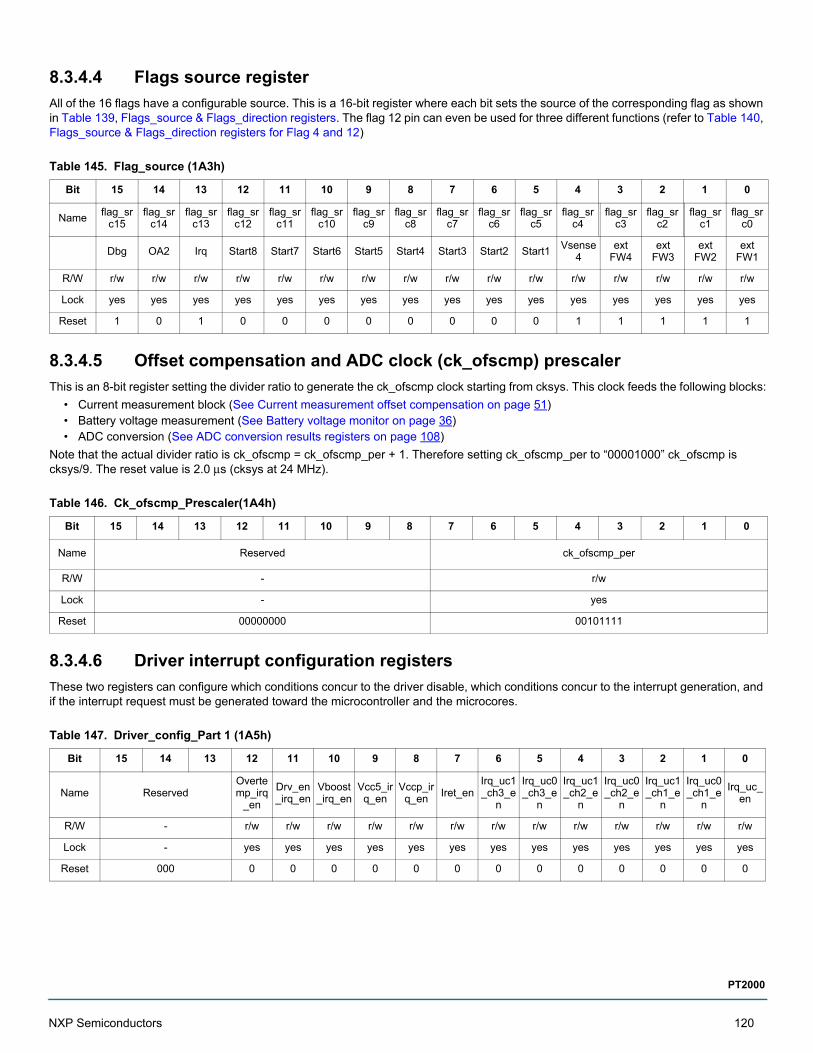
8.3.4.4 Flags source register
All of the 16 flags have a configurable source. This is a 16-bit register where each bit sets the source of the corresponding flag as shown in Table 139, Flags_source & Flags_direction registers. The flag 12 pin can even be used for three different functions (refer to Table 140, Flags_source & Flags_direction registers for Flag 4 and 12)
8.3.4.5 Offset compensation and ADC clock (ck_ofscmp) prescaler
This is an 8-bit register setting the divider ratio to generate the ck_ofscmp clock starting from cksys. This clock feeds the following blocks:
• Current measurement block (See Current measurement offset compensation on page 51)• Battery voltage measurement (See Battery voltage monitor on page 36)• ADC conversion (See ADC conversion results registers on page 108)
Note that the actual divider ratio is ck_ofscmp = ck_ofscmp_per + 1. Therefore setting ck_ofscmp_per to “00001000” ck_ofscmp is cksys/9. The reset value is 2.0 μs (cksys at 24 MHz).
8.3.4.6 Driver interrupt configuration registers
These two registers can configure which conditions concur to the driver disable, which conditions concur to the interrupt generation, and if the interrupt request must be generated toward the microcontroller and the microcores.
Table 145. Flag_source (1A3h)
Bit 15 14 13 12 11 10 9 8 7 6 5 4 3 2 1 0
Nameflag_sr
c15flag_sr
c14flag_sr
c13flag_sr
c12flag_sr
c11flag_sr
c10flag_sr
c9flag_sr
c8flag_sr
c7flag_sr
c6flag_sr
c5flag_sr
c4flag_sr
c3flag_sr
c2flag_sr
c1flag_sr
c0
Dbg OA2 Irq Start8 Start7 Start6 Start5 Start4 Start3 Start2 Start1Vsense
4ext
FW4ext
FW3ext
FW2ext
FW1
R/W r/w r/w r/w r/w r/w r/w r/w r/w r/w r/w r/w r/w r/w r/w r/w r/w
Lock yes yes yes yes yes yes yes yes yes yes yes yes yes yes yes yes
Reset 1 0 1 0 0 0 0 0 0 0 0 1 1 1 1 1
Table 146. Ck_ofscmp_Prescaler(1A4h)
Bit 15 14 13 12 11 10 9 8 7 6 5 4 3 2 1 0
Name Reserved ck_ofscmp_per
R/W - r/w
Lock - yes
Reset 00000000 00101111
Table 147. Driver_config_Part 1 (1A5h)
Bit 15 14 13 12 11 10 9 8 7 6 5 4 3 2 1 0
Name ReservedOvertemp_irq
_en
Drv_en_irq_en
Vboost_irq_en
Vcc5_irq_en
Vccp_irq_en
Iret_enIrq_uc1_ch3_e
n
Irq_uc0_ch3_e
n
Irq_uc1_ch2_e
n
Irq_uc0_ch2_e
n
Irq_uc1_ch1_e
n
Irq_uc0_ch1_e
n
Irq_uc_en
R/W - r/w r/w r/w r/w r/w r/w r/w r/w r/w r/w r/w r/w r/w
Lock - yes yes yes yes yes yes yes yes yes yes yes yes yes
Reset 000 0 0 0 0 0 0 0 0 0 0 0 0 0
NXP Semiconductors 120
PT2000
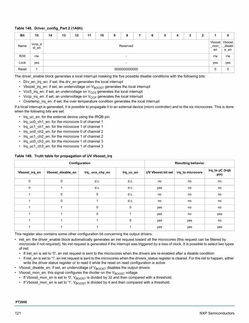
The driver_enable block generates a local interrupt masking the five possible disable conditions with the following bits:
• Drv_en_irq_en: if set, the drv_en generates the local interrupt• Vboost_irq_en: if set, an undervoltage on VBOOST generates the local interrupt• Vcc5_irq_en: if set, an undervoltage on VCC5 generates the local interrupt• Vccp_irq_en: if set, an undervoltage on VCCP generates the local interrupt• Overtemp_irq_en: if set, the over temperature condition generates the local interrupt
If a local interrupt is generated, it is possible to propagate it to an external device (micro controller) and to the six microcores. This is done when the following bits are set:
• Irq_uc_en, for the external device using the IRQB pin• Irq_uc0_ch1_en, for the microcore 0 of channel 1• Irq_uc1_ch1_en, for the microcore 1 of channel 1• Irq_uc0_ch2_en, for the microcore 0 of channel 2• Irq_uc1_ch2_en, for the microcore 1 of channel 2• Irq_uc0_ch3_en, for the microcore 1 of channel 3• Irq_uc1_ch3_en, for the microcore 1 of channel 3
This register also contains some other configuration bit concerning the output drivers:
• iret_en: the driver_enable block automatically generates an iret request toward all the microcores (this request can be filtered by microcode if not required). No iret request is generated if the interrupt was triggered by a loss of clock. It is possible to select two types of iret:• If iret_en is set to '0', an iret request is sent to the microcores when the drivers are re-enabled after a disable condition• If iret_en is set to '1', an iret request is sent to the microcores when the drivers_status register is cleared. For the iret to happen, either
write the driver status register or to read it while the reset on read configuration is active• Vboost_disable_en: if set, an undervoltage of VBOOST disables the output drivers• Vboost_mon_en: this signal configures the divider on the VBOOST voltage
• If Vboost_mon_en is set to '0', VBOOST is divided by 32 and then compared with a threshold.• If Vboost_mon_en is set to '1', VBOOST is divided by 4 and then compared with a threshold.
Table 148. Driver_config_Part 2 (1A6h)
Bit 15 14 13 12 11 10 9 8 7 6 5 4 3 2 1 0
Namevccp_ext_en
ReservedVboost_mon_
en
Vboost_disable_en
R/W r/w - r/w r/w
Lock yes - yes yes
Reset 1 0000000000000 0 0
Table 149. Truth table for propagation of UV Vboost_irq
Configuration Resulting behavior
Vboost_irq_en Vboost_disable_en Irq_ ucx_chy_en Irq_uc_en UV Vboost bit set irq_to microcoreirq_to µC (Irqb
pin)
0 0 d.c. d.c. no no no
0 1 d.c. d.c. yes no no
1 0 0 d.c. no no no
1 0 1 d.c. no no no
1 1 0 0 yes no no
1 1 0 1 yes no yes
1 1 1 0 yes yes no
1 1 1 1 yes yes yes
121 NXP Semiconductors
PT2000

• vccp_ext_enable: if set to '0', the internal voltage regulator is enabled and the corresponding pin is used only to connect a bypass capacitor. If set to '1', the internal voltage regulator is disabled and the VCCP voltage must be supplied externally through the corresponding pin. During bootstrap switch init (See Bootstrap switch control on page 58), this setting is bypassed and the value of the vccp_ext_enable signal is set to the inverted value of the DBG pin sampled at reset (POResetB and ResetB). This is better defined in Table 150, VCCP external enable setting. This means the DBG pin, at reset, needs to be configured as an input whose value is latched at the rising edge of the POResetB and ResetB signal, and used to set the configuration of the VCCP internal regulator during the init phase of the bootstrap switch. A SPI reset leaves the latched information unchanged. The DBG pin has an internal weak pull-up resistor so its value is '1' when not connected (n.c.).
8.3.4.7 PLL factor and speed configuration register
• PLL_factor: if set to '0', the PLL multiplication factor is 12, otherwise it is 24• PLL_spread_disable: if set to '0' the PLL output clock has a spread, otherwise it has no spread
The PLL factor is changed synchronously with clock monitor cycle to avoid a clock monitor alert when changing between 12 MHz and 24 MHz. This register is reset by POReset, ResetB, and the SPI reset.
8.3.4.8 Backup clock status register
This 11-bit register is meant to provide the external microcontroller a way to monitor the status of the clock signal. This is done by latching the information occurring on a switch to the backup_reference signal:
• Timing_violation: this bit is set if a timing violation was detected. Writing a '1' value on this register bit, resets the timing violation information
• Loss_of_clock: this read_only bit (loss_of_clock) latches the condition when the input reference is missing
Table 150. VCCP external enable setting
dbg pin (latched) SPI bit BS Init (min. 1 HS) VCCP external enable
1 (n.c.) - 1 0 (internal reg ON)
1 (n.c.) 1 0 1 (internal reg OFF)
1 (n.c.) 0 0 0 (internal reg ON)
0 1 - 1 (internal reg OFF)
0 0 - 0 (internal reg ON)
Table 151. PLL_Config (1A7h)
Bit 15 14 13 12 11 10 9 8 7 6 5 4 3 2 1 0
Name ReservedPLL_spread_disabl
e
PLL_factor
R/W - r/w r/w
Lock - yes yes
Reset 00000000000000 0 1
Table 152. backup_clock_status (1A8h)
Bit 15 14 13 12 11 10 9 8 7 6 5 4 3 2 1 0
NameTiming_violation
cksys_missing_disable_driv
er
Reserveduc1_ch3_irq_e
n
uc0_ch3_irq_e
n
uc1_ch2 rq en
uc0_ch2_irq_e
n
uc1_ch1_irq_e
n
uc0_ch1_irq_e
n
uc_irq_en
switch_to_clock_pi
n
loss_of_clock
R/W r/w r/w - r/w r/w r/w r/w r/w r/w r/w r/w r
Lock no yes - yes yes yes yes yes yes yes no no
Reset 0 0 00000 0 0 0 0 0 0 0 0 0
NXP Semiconductors 122
PT2000

• Switch_to_clock_pin: this bit (active on rising edge) is used to provide a way to reset the loss of clock condition. If this bit is set during a loss of clock condition it is reset as soon as the clock manager switches the PLL input to the external reference. If this bit sets while there is no loss of clock, the bit resets immediately without any effect. For further details refer to See BIST on page 64
• uc_irq_en: enable the generation of an interrupt request to the external micro controller when cksys missing is detected. This interrupt is active until this register is read
• uc0_ch1_irq_en: enable the generation of an interrupt request to microcore 0 channel 1 when cksys missing is detected• uc1_ch1_irq_en: enable the generation of an interrupt request to microcore 1 channel 1 when cksys missing is detected• uc0_ch2_irq_en: enable the generation of an interrupt request to microcore 0 channel 2 when cksys missing is detected• uc1_ch2_irq_en: enable the generation of an interrupt request to microcore 1 channel 2 when cksys missing is detected• uc0_ch3_irq_en: enable the generation of an interrupt request to microcore 0 channel 3 when cksys missing is detected• uc1_ch3_irq_en: enable the generation of an interrupt request to microcore 1 channel 3 when cksys missing is detected• cksys_missing_disable_driver: if set, the output drivers are disabled via the signal cksys_drven as long as the cksys_missing signal
is '1'.
Once the loss_of_clock bit sets, it can be reset only by completing a “switch to clock” pin. For this operation to complete, it must be requested when the main clock input pin again provides a valid clock frequency.
The interrupt to the external micro and to the microcores is triggered as long as the cksys_missing signal is set. The microcore is able to process the interrupt as soon as there is a clock available. It is triggered every time the clock manager switches to the internal clock reference and when the clock manager tries to switch back to the external clock reference, due to a SPI request. The interrupt can even occur multiple times during cksys_missing state.
8.3.4.9 SPI configuration register
The spi_config register (address 1A9h) is an 8-bit register storing the SPI protocol configuration and SPI diagnostics.
• Miso_slewrate: selects one of the two possible values for the slew rate of the MISO pin.• 0 slow slew rate • 1 fast slew rate
• Protocol_mode: select the type of burst transmission accepted by the protocol, '0' means mode A, '1' means mode B.• irq_enable: enable the SPI interface to request an interrupt toward the microcontroller if an incorrect SPI transmission is received.• Watchdog: when using mode A, the maximum time the SPI chip select can be inactive during a burst is expressed as follows:
tWATCHDOG = tCKSYS ((watchdog + 1) ≠ 32768)where tCKSYS is the period of the cksys internal clock.
When changing the SPI protocol mode by a write access to this register, it has to be done using a SPI transmission which is compatible to mode A and B (see See Mode A on page 77 and See Mode B on page 78). This means it must not use '0' as number of operations for the SPI transmission, and must not deassert the chip select during the transmission. Changing the protocol mode can be done as often as required.
Table 153. Spi_config (1A9h)
Bit 15 14 13 12 11 10 9 8 7 6 5 4 3 2 1 0
Name ReservedMISO_sle
wrateprotocol_
modeirq_en watchdog
R/W - r/w r/w r/w r/w
Lock - yes yes yes yes
Reset 00000000 0 0 0 01010
123 NXP Semiconductors
PT2000
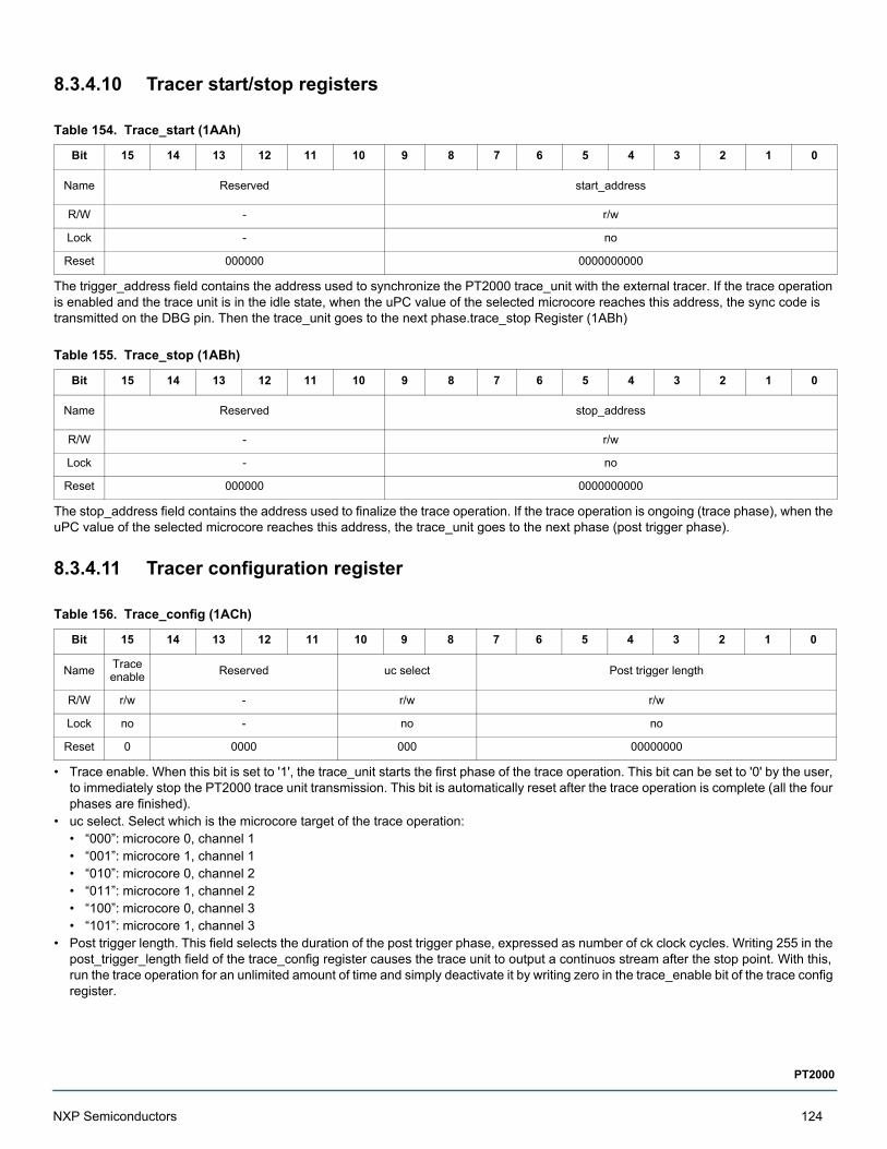
8.3.4.10 Tracer start/stop registers
The trigger_address field contains the address used to synchronize the PT2000 trace_unit with the external tracer. If the trace operation is enabled and the trace unit is in the idle state, when the uPC value of the selected microcore reaches this address, the sync code is transmitted on the DBG pin. Then the trace_unit goes to the next phase.trace_stop Register (1ABh)
The stop_address field contains the address used to finalize the trace operation. If the trace operation is ongoing (trace phase), when the uPC value of the selected microcore reaches this address, the trace_unit goes to the next phase (post trigger phase).
8.3.4.11 Tracer configuration register
• Trace enable. When this bit is set to '1', the trace_unit starts the first phase of the trace operation. This bit can be set to '0' by the user, to immediately stop the PT2000 trace unit transmission. This bit is automatically reset after the trace operation is complete (all the four phases are finished).
• uc select. Select which is the microcore target of the trace operation:• “000”: microcore 0, channel 1• “001”: microcore 1, channel 1• “010”: microcore 0, channel 2• “011”: microcore 1, channel 2• “100”: microcore 0, channel 3• “101”: microcore 1, channel 3
• Post trigger length. This field selects the duration of the post trigger phase, expressed as number of ck clock cycles. Writing 255 in the post_trigger_length field of the trace_config register causes the trace unit to output a continuos stream after the stop point. With this, run the trace operation for an unlimited amount of time and simply deactivate it by writing zero in the trace_enable bit of the trace config register.
Table 154. Trace_start (1AAh)
Bit 15 14 13 12 11 10 9 8 7 6 5 4 3 2 1 0
Name Reserved start_address
R/W - r/w
Lock - no
Reset 000000 0000000000
Table 155. Trace_stop (1ABh)
Bit 15 14 13 12 11 10 9 8 7 6 5 4 3 2 1 0
Name Reserved stop_address
R/W - r/w
Lock - no
Reset 000000 0000000000
Table 156. Trace_config (1ACh)
Bit 15 14 13 12 11 10 9 8 7 6 5 4 3 2 1 0
NameTrace enable
Reserved uc select Post trigger length
R/W r/w - r/w r/w
Lock no - no no
Reset 0 0000 000 00000000
NXP Semiconductors 124
PT2000
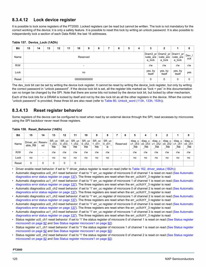
8.3.4.12 Lock device register
It is possible to lock some registers of the PT2000. Locked registers can be read but cannot be written. The lock is not mandatory for the correct working of the device; it is only a safety feature. It is possible to reset this lock by writing an unlock password. It is also possible to independently lock a section of each Data RAM, the last 16 addresses.
The dev_lock bit can be set by writing the device lock register. It cannot be reset by writing the device_lock register, but only by writing the correct password in “unlock password”. If the device lock bit is set, all the register bits marked as “lock = yes” in this documentation can no longer be changed by the SPI. Note that there are some bits not locked by the device lock bit, but locked by other mechanism.
Each of the lock bits for a DRAM is locked by itself and not by the dev lock bit as all the other registers in the device. When the correct “unlock password” is provided, these three bit are also reset (refer to Table 80, Unlock_word (113h, 133h, 153h)).
8.3.4.13 Reset register behavior
Some registers of the device can be configured to reset when read by an external device through the SPI; read accesses by microcores using the SPI backdoor never reset those registers.
• Driver enable reset behavior: if set to '1' driver_status register is reset on read (refer to Table 162, driver_status (1B2h))• Automatic diagnostics uc0_ch1 reset behavior: if set to '1' err_uc register of microcore 0 of channel 1 is reset on read (See Automatic
diagnostics error status register on page 137). The three registers are reset when the err_ucXchY_3 register is read• Automatic diagnostics uc1_ch1 reset behavior: if set to '1' err_uc register of microcore 1 of channel 1 is reset on read (See Automatic
diagnostics error status register on page 137). The three registers are reset when the err_ucXchY_3 register is read• Automatic diagnostics uc0_ch2 reset behavior: if set to '1' err_uc register of microcore 0 of channel 2 is reset on read (See Automatic
diagnostics error status register on page 137). The three registers are reset when the err_ucXchY_3 register is read• Automatic diagnostics uc1_ch2 reset behavior: if set to '1' err_uc register of microcore 1 of channel 2 is reset on read (See Automatic
diagnostics error status register on page 137). The three registers are reset when the err_ucXchY_3 register is read• Automatic diagnostics uc0_ch3 reset behavior: if set to '1' err_uc register of microcore 0 of channel 3 is reset on read (See Automatic
diagnostics error status register on page 137). The three registers are reset when the err_ucXchY_3 register is read• Automatic diagnostics uc1_ch3 reset behavior: if set to '1' err_uc register of microcore 1 of channel 3 is reset on read (See Automatic
diagnostics error status register on page 137). The three registers are reset when the err_ucXchY_3 register is read• Status register uc0_ch1 reset behavior: if set to '1' the status register of microcore 0 of channel 1 is reset on read (See Status register
microcore0 on page 92 and See Status register microcore1 on page 92)• Status register uc1_ch1 reset behavior: if set to '1' the status register of microcore 1 of channel 1 is reset on read (See Status register
microcore0 on page 92 and See Status register microcore1 on page 92)• Status register uc0_ch2 reset behavior: if set to '1' the status register of microcore 0 of channel 2 is reset on read (See Status register
microcore0 on page 92 and See Status register microcore1 on page 92)
Table 157. Device_Lock (1ADh)
Bit 15 14 13 12 11 10 9 8 7 6 5 4 3 2 1 0
Name ReservedDram3_private_are
a_lock
Dram2_private_are
a_lock
Dram1_private_are
a_lock
Dev_lock
R/W - r/w r/w r/w r/w
Lock noyes, by itself
yes, by itself
yes, by itself
yes
Reset 000000000000 0 0 0 0
Table 158. Reset_Behavior (1AEh)
Bit 15 14 13 12 11 10 9 8 7 6 5 4 3 2 1 0
NameDriver_enable_RB
Reserved
SR_uc1_ch3_
RB
SR_uc0_ch3_
RB
SR_uc1_ch2_
RB
SR_uc0_ch2_
RB
SR_uc1_ch1_
RB
SR_uc0_ch1_
BReserved
diag_uc1_ch3
_RB
diag_uc0_ch3
_RB
diag_uc1_ch2
_RB
diag_uc0_ch2
_RB
diag_uc1_ch1
_RB
diag_uc0_ch1
_RB
R/W r/w - r/w r/w r/w r/w r/w r/w - r/w r/w r/w r/w r/w r/w
Lock no - no no no no no no - no no no no no no
Reset 0 0 0 0 0
125 NXP Semiconductors
PT2000
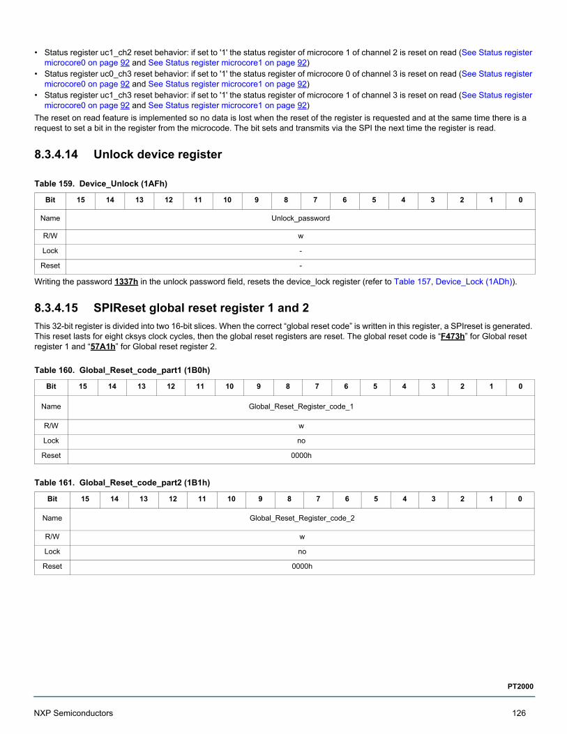
• Status register uc1_ch2 reset behavior: if set to '1' the status register of microcore 1 of channel 2 is reset on read (See Status register microcore0 on page 92 and See Status register microcore1 on page 92)
• Status register uc0_ch3 reset behavior: if set to '1' the status register of microcore 0 of channel 3 is reset on read (See Status register microcore0 on page 92 and See Status register microcore1 on page 92)
• Status register uc1_ch3 reset behavior: if set to '1' the status register of microcore 1 of channel 3 is reset on read (See Status register microcore0 on page 92 and See Status register microcore1 on page 92)
The reset on read feature is implemented so no data is lost when the reset of the register is requested and at the same time there is a request to set a bit in the register from the microcode. The bit sets and transmits via the SPI the next time the register is read.
8.3.4.14 Unlock device register
Writing the password 1337h in the unlock password field, resets the device_lock register (refer to Table 157, Device_Lock (1ADh)).
8.3.4.15 SPIReset global reset register 1 and 2
This 32-bit register is divided into two 16-bit slices. When the correct “global reset code” is written in this register, a SPIreset is generated. This reset lasts for eight cksys clock cycles, then the global reset registers are reset. The global reset code is “F473h” for Global reset register 1 and “57A1h” for Global reset register 2.
Table 159. Device_Unlock (1AFh)
Bit 15 14 13 12 11 10 9 8 7 6 5 4 3 2 1 0
Name Unlock_password
R/W w
Lock -
Reset -
Table 160. Global_Reset_code_part1 (1B0h)
Bit 15 14 13 12 11 10 9 8 7 6 5 4 3 2 1 0
Name Global_Reset_Register_code_1
R/W w
Lock no
Reset 0000h
Table 161. Global_Reset_code_part2 (1B1h)
Bit 15 14 13 12 11 10 9 8 7 6 5 4 3 2 1 0
Name Global_Reset_Register_code_2
R/W w
Lock no
Reset 0000h
NXP Semiconductors 126
PT2000
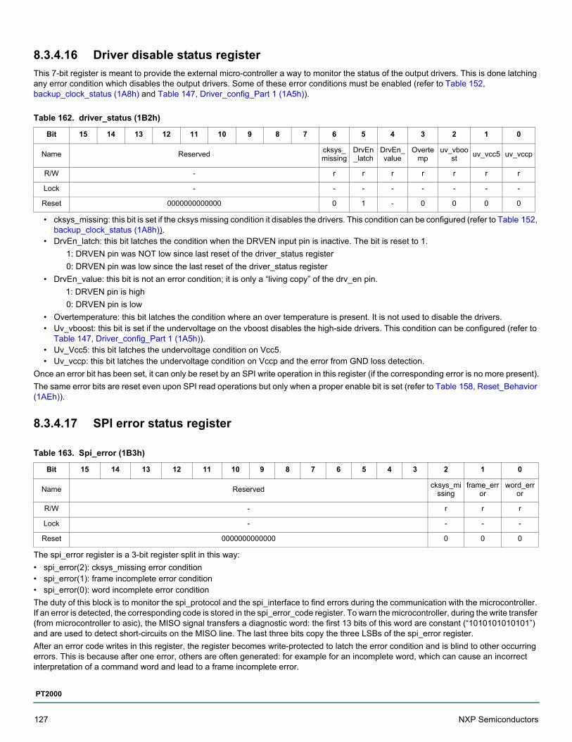
8.3.4.16 Driver disable status register
This 7-bit register is meant to provide the external micro-controller a way to monitor the status of the output drivers. This is done latching any error condition which disables the output drivers. Some of these error conditions must be enabled (refer to Table 152, backup_clock_status (1A8h) and Table 147, Driver_config_Part 1 (1A5h)).
• cksys_missing: this bit is set if the cksys missing condition it disables the drivers. This condition can be configured (refer to Table 152, backup_clock_status (1A8h)).
• DrvEn_latch: this bit latches the condition when the DRVEN input pin is inactive. The bit is reset to 1.
1: DRVEN pin was NOT low since last reset of the driver_status register
0: DRVEN pin was low since the last reset of the driver_status register
• DrvEn_value: this bit is not an error condition; it is only a “living copy” of the drv_en pin.
1: DRVEN pin is high
0: DRVEN pin is low
• Overtemperature: this bit latches the condition where an over temperature is present. It is not used to disable the drivers. • Uv_vboost: this bit is set if the undervoltage on the vboost disables the high-side drivers. This condition can be configured (refer to
Table 147, Driver_config_Part 1 (1A5h)).• Uv_Vcc5: this bit latches the undervoltage condition on Vcc5.• Uv_vccp: this bit latches the undervoltage condition on Vccp and the error from GND loss detection.
Once an error bit has been set, it can only be reset by an SPI write operation in this register (if the corresponding error is no more present).
The same error bits are reset even upon SPI read operations but only when a proper enable bit is set (refer to Table 158, Reset_Behavior (1AEh)).
8.3.4.17 SPI error status register
The spi_error register is a 3-bit register split in this way:
• spi_error(2): cksys_missing error condition• spi_error(1): frame incomplete error condition• spi_error(0): word incomplete error condition
The duty of this block is to monitor the spi_protocol and the spi_interface to find errors during the communication with the microcontroller. If an error is detected, the corresponding code is stored in the spi_error_code register. To warn the microcontroller, during the write transfer (from microcontroller to asic), the MISO signal transfers a diagnostic word: the first 13 bits of this word are constant (“1010101010101”) and are used to detect short-circuits on the MISO line. The last three bits copy the three LSBs of the spi_error register.
After an error code writes in this register, the register becomes write-protected to latch the error condition and is blind to other occurring errors. This is because after one error, others are often generated: for example for an incomplete word, which can cause an incorrect interpretation of a command word and lead to a frame incomplete error.
Table 162. driver_status (1B2h)
Bit 15 14 13 12 11 10 9 8 7 6 5 4 3 2 1 0
Name Reservedcksys_missing
DrvEn_latch
DrvEn_value
Overtemp
uv_vboost
uv_vcc5 uv_vccp
R/W - r r r r r r r
Lock - - - - - - - -
Reset 0000000000000 0 1 - 0 0 0 0
Table 163. Spi_error (1B3h)
Bit 15 14 13 12 11 10 9 8 7 6 5 4 3 2 1 0
Name Reservedcksys_mi
ssingframe_err
orword_err
or
R/W - r r r
Lock - - - -
Reset 0000000000000 0 0 0
127 NXP Semiconductors
PT2000

By latching only the first occurring error, it is possible to read the cause of the failure in the communication, without having to see all the side effects. Furthermore, the PT2000 has the possibility to generate an interrupt request toward the microcontroller by setting the appropriate bit in the spi_config register (refer to Table 153, Spi_config (1A9h)).
When an error is met in the SPI connection, the SPI protocol inside the PT2000 moves to a state where it only accepts a specific two word SPI transmission with command word (B661h) meant to read the spi_error register (refer to Table 163, Spi_error (1B3h)). This command causes the device to transmit a single word to the SPI master and then reset the protocol (along with the interrupt if enabled). If the value of the selection register was set to the value 0100h (selecting the generic configuration registers) before the error, the word transmitted is the error code and the error code register is reset immediately, otherwise a random word is sent and the error state of the SPI protocol is reset. In this second case, the error code register can be read (and thus reset) in a following burst. The following are the possible kind of errors and their relative codes (during correct operations the value of the register is 0000h).
• cksys_missing: this error is set if a SPI transfer is required (which means if the SPI chip select CSB is pulled low) while the cksys clock is missing.
• frame_error: this error is set if the number of data words in a burst is not the expected number programmed in the command word:• Mode A is selected, the slave_protocol block received a control word specifying n word transfers, but the microcontroller performs
less operations and then ends the communication. In this case, this module provides a watchdog function if during a programmed transfer, the communication with the microcontroller is inactive for a time longer than a prefixed limit, so the transfer is considered aborted and an error is detected.
• Mode B is selected, the number parameter is not zero in the command word and the number of transferred words is different from the one programmed in the command word.
• A frame error can also occur when the access limitations to DRAM in dual sequencer mode at maximum ck are violated (refer to Table 49)
• word_error: during the transfer of a word long data, the device receives or sends an incorrect number of bits (15 or 17 instead of 16, for example). If multiple words are being transferred in a row with the chip select always active (the fastest way), the error is detected at the end of the sequence and it is not possible to say which is the incorrect word. To be sure of the incorrect data, the chip select must be deactivated and reactivated between each word transfer.
8.3.4.18 Interruption status registers
These two registers latch the status of all the interrupt requests toward the external microcontroller. They also latch the halt signal generated by the automatic diagnostics toward the six microcores.
Table 164. Interrupt_Register_Part1 (1B4h)
Bit 15 14 13 12 11 10 9 8 7 6 5 4 3 2 1 0
Name Reservedirq_uc1_ch3
irq_uc0_ch3
irq_uc1_ch2
irq_uc0_ch2
irq_uc1_ch1
irq_uc0_ch1
Reservedhalt_uc1_ch3
halt_uc0_ch3
halt_uc1_ch2
halt_uc0_ch2
halt_uc1_ch1
halt_uc0_ch1
R/W - r r r r r r - r r r r r r
Lock no no no no no no no no no no no no no no
Reset 00 0 0 0 0 0 0 00 0 0 0 0 0 0
Table 165. Interrupt_Register_Part2 (1B5h)
Bit 15 14 13 12 11 10 9 8 7 6 5 4 3 2 1 0
Name Reservedchecksum_ch3
checksum_ch
2
checksum_ch
1
cksys_missin
gSPI_irq drv_irq Reserved
R/W - r r r r r r -
Lock no no no no no no no no
Reset 00 0 0 0 0 0 0 00000000
NXP Semiconductors 128
PT2000
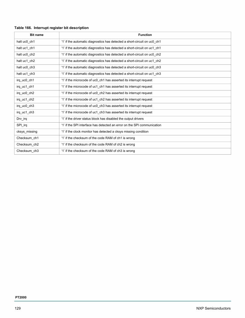
Table 166. Interrupt register bit description
Bit name Function
halt uc0_ch1 ‘1’ if the automatic diagnostics has detected a short-circuit on uc0_ch1
halt uc1_ch1 ‘1’ if the automatic diagnostics has detected a short-circuit on uc1_ch1
halt uc0_ch2 ‘1’ if the automatic diagnostics has detected a short-circuit on uc0_ch2
halt uc1_ch2 ‘1’ if the automatic diagnostics has detected a short-circuit on uc1_ch2
halt uc0_ch3 ‘1’ if the automatic diagnostics has detected a short-circuit on uc0_ch3
halt uc1_ch3 ‘1’ if the automatic diagnostics has detected a short-circuit on uc1_ch3
irq_uc0_ch1 ‘1’ if the microcode of uc0_ch1 has asserted its interrupt request
irq_uc1_ch1 ‘1’ if the microcode of uc1_ch1 has asserted its interrupt request
irq_uc0_ch2 ‘1’ if the microcode of uc0_ch2 has asserted its interrupt request
irq_uc1_ch2 ‘1’ if the microcode of uc1_ch2 has asserted its interrupt request
irq_uc0_ch3 ‘1’ if the microcode of uc0_ch3 has asserted its interrupt request
irq_uc1_ch3 ‘1’ if the microcode of uc1_ch3 has asserted its interrupt request
Drv_irq ‘1’ if the driver status block has disabled the output drivers
SPI_irq ‘1’ if the SPI interface has detected an error on the SPI communication
cksys_missing ‘1’ if the clock monitor has detected a cksys missing condition
Checksum_ch1 ‘1’ if the checksum of the code RAM of ch1 is wrong
Checksum_ch2 ‘1’ if the checksum of the code RAM of ch2 is wrong
Checksum_ch3 ‘1’ if the checksum of the code RAM of ch3 is wrong
129 NXP Semiconductors
PT2000
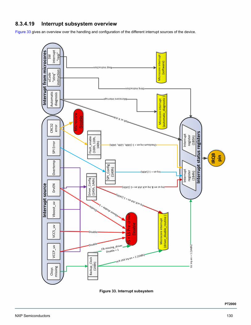
8.3.4.19 Interrupt subsystem overview
Figure 33 gives an overview over the handling and configuration of the different interrupt sources of the device.
Figure 33. Interrupt subsystem
Cksy
sm
issin
gVC
CP_u
vVC
C5_u
vVb
oost
_uv
DrvE
NO
vert
emp
SPI E
rror
CRC3
2er
ror
Auto
mat
ic
diag
nosis
uCod
e �s
tirq�
in
stru
ctio
n
Inte
rrup
t sou
rce
Mic
roco
re in
terr
upt
(driv
er_d
isabl
e_ro
utin
e )
Mic
roco
re in
terr
upt
(aut
omat
ic_d
iagn
ostic
)M
icro
core
inte
rrup
t (s
oftw
are)
IRQ
B pi
n
SW
inte
rrup
t �r
eqi�
Inte
rrup
t re
gist
er
(1B4
h)
Inte
rrup
t re
gist
er
(1B5
h)
HS +
LS
Pre-
driv
erDi
sabl
e
Mic
roco
reDi
sabl
e
SPI_
Conf
ig(1
A9h)
Flas
h_en
able
(100
h, 1
20h,
14
0h)
Microcore interrupt
Disable
Disable
Disable
Clk missing_driver
Disable = 1
Driv
er_C
onfig
(1A5
h, 1
A6h)
Irq uc en & irq ucX chX en =1 (1A5h)
Uc
irq e
n =
1 (1
A8h)
Irq en = 1 (1A9h)
Checksum irq en = 1 (100h, 120h, 140h)
Stirq instruction
Reqi instruction
Back
up_C
lock
(1A8
h) ucX chX irq en = 1 (1A8h)
Inte
rrup
t sta
tus r
egis
ters
Halt uc X chX
Irq ucX chX en = 1 (1A5h)
Vboost disable = 1
Inte
rrup
t fro
m m
icro
core
s
NXP Semiconductors 130
PT2000
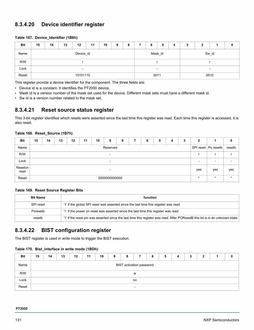
8.3.4.20 Device identifier register
This register provide a device identifier for the component. The three fields are:
• Device id is a constant. It identifies the PT2000 device.• Mask id is a version number of the mask set used for the device. Different mask sets must have a different mask id.• Sw id is a version number related to the mask set.
8.3.4.21 Reset source status register
This 3-bit register identifies which resets were asserted since the last time this register was read. Each time this register is accessed, it is also reset.
8.3.4.22 BIST configuration register
The BIST register is used in write mode to trigger the BIST execution.
Table 167. Device_Identifier (1B6h)
Bit 15 14 13 12 11 10 9 8 7 6 5 4 3 2 1 0
Name Device_id Mask_id Sw_id
R/W r r r
Lock - - -
Reset 10101110 0011 0010
Table 168. Reset_Source (1B7h)
Bit 15 14 13 12 11 10 9 8 7 6 5 4 3 2 1 0
Name Reserved SPI reset Po resetb resetb
R/W - r r r
Lock - - - -
Reseton read
- yes yes yes
Reset 0000000000000 * * *
Table 169. Reset Source Register Bits
Bit Name function
SPI reset ‘1’ if the global SPI reset was asserted since the last time this register was read
Poresetb ‘1’ if the power on reset was asserted since the last time this register was read
resetb ‘1’ if the reset pin was asserted since the last time this register was read. After POResetB this bit is in an unknown state.
Table 170. Bist_interface in write mode (1BDh)
Bit 15 14 13 12 11 10 9 8 7 6 5 4 3 2 1 0
Name BIST activation password
R/W w
Lock no
Reset -
131 NXP Semiconductors
PT2000
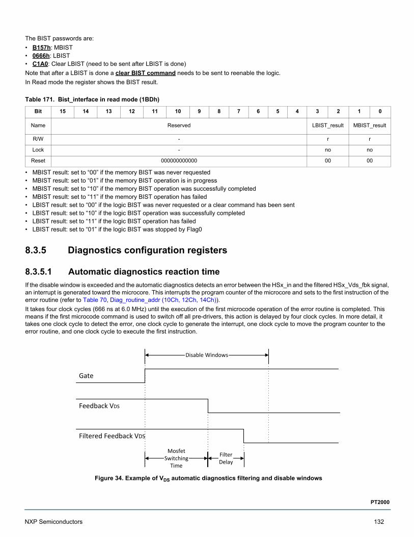
The BIST passwords are:
• B157h: MBIST• 0666h: LBIST• C1A0: Clear LBIST (need to be sent after LBIST is done)
Note that after a LBIST is done a clear BIST command needs to be sent to reenable the logic.
In Read mode the register shows the BIST result.
• MBIST result: set to “00” if the memory BIST was never requested• MBIST result: set to “01” if the memory BIST operation is in progress• MBIST result: set to “10” if the memory BIST operation was successfully completed• MBIST result: set to “11” if the memory BIST operation has failed• LBIST result: set to “00” if the logic BIST was never requested or a clear command has been sent• LBIST result: set to “10” if the logic BIST operation was successfully completed• LBIST result: set to “11” if the logic BIST operation has failed• LBIST result: set to “01” if the logic BIST was stopped by Flag0
8.3.5 Diagnostics configuration registers
8.3.5.1 Automatic diagnostics reaction time
If the disable window is exceeded and the automatic diagnostics detects an error between the HSx_in and the filtered HSx_Vds_fbk signal, an interrupt is generated toward the microcore. This interrupts the program counter of the microcore and sets to the first instruction of the error routine (refer to Table 70, Diag_routine_addr (10Ch, 12Ch, 14Ch)).
It takes four clock cycles (666 ns at 6.0 MHz) until the execution of the first microcode operation of the error routine is completed. This means if the first microcode command is used to switch off all pre-drivers, this action is delayed by four clock cycles. In more detail, it takes one clock cycle to detect the error, one clock cycle to generate the interrupt, one clock cycle to move the program counter to the error routine, and one clock cycle to execute the first instruction.
Figure 34. Example of VDS automatic diagnostics filtering and disable windows
Table 171. Bist_interface in read mode (1BDh)
Bit 15 14 13 12 11 10 9 8 7 6 5 4 3 2 1 0
Name Reserved LBIST_result MBIST_result
R/W - r r
Lock - no no
Reset 000000000000 00 00
Disable Windows
Gate
Feedback VDS
Filtered Feedback VDS
MosfetSwitching
Time
FilterDelay
NXP Semiconductors 132
PT2000
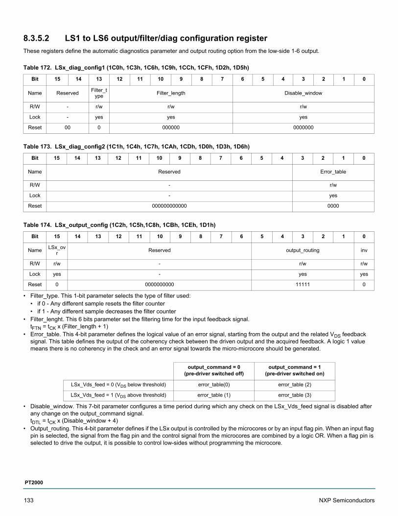
8.3.5.2 LS1 to LS6 output/filter/diag configuration register
These registers define the automatic diagnostics parameter and output routing option from the low-side 1-6 output.
• Filter_type. This 1-bit parameter selects the type of filter used:• if 0 - Any different sample resets the filter counter• if 1 - Any different sample decreases the filter counter
• Filter_lenght. This 6 bits parameter set the filtering time for the input feedback signal. tFTN = tCK x (Filter_length + 1)
• Error_table. This 4-bit parameter defines the logical value of an error signal, starting from the output and the related VDS feedback signal. This table defines the output of the coherency check between the driven output and the acquired feedback. A logic 1 value means there is no coherency in the check and an error signal towards the micro-microcore should be generated.
• Disable_window. This 7-bit parameter configures a time period during which any check on the LSx_Vds_feed signal is disabled after any change on the output_command signal. tDTL = tCK x (Disable_window + 4)
• Output_routing. This 4-bit parameter defines if the LSx output is controlled by the microcores or by an input flag pin. When an input flag pin is selected, the signal from the flag pin and the control signal from the microcores are combined by a logic OR. When a flag pin is selected to drive the output, it is possible to control low-sides without programming the microcore.
Table 172. LSx_diag_config1 (1C0h, 1C3h, 1C6h, 1C9h, 1CCh, 1CFh, 1D2h, 1D5h)
Bit 15 14 13 12 11 10 9 8 7 6 5 4 3 2 1 0
Name ReservedFilter_t
ypeFilter_length Disable_window
R/W - r/w r/w r/w
Lock - yes yes yes
Reset 00 0 000000 0000000
Table 173. LSx_diag_config2 (1C1h, 1C4h, 1C7h, 1CAh, 1CDh, 1D0h, 1D3h, 1D6h)
Bit 15 14 13 12 11 10 9 8 7 6 5 4 3 2 1 0
Name Reserved Error_table
R/W - r/w
Lock - yes
Reset 000000000000 0000
Table 174. LSx_output_config (1C2h, 1C5h,1C8h, 1CBh, 1CEh, 1D1h)
Bit 15 14 13 12 11 10 9 8 7 6 5 4 3 2 1 0
NameLSx_ov
rReserved output_routing inv
R/W r/w - r/w r/w
Lock yes - yes yes
Reset 0 0000000000 11111 0
output_command = 0(pre-driver switched off)
output_command = 1(pre-driver switched on)
LSx_Vds_feed = 0 (VDS below threshold) error_table(0) error_table (2)
LSx_Vds_feed = 1 (VDS above threshold) error_table (1) error_table (3)
133 NXP Semiconductors
PT2000
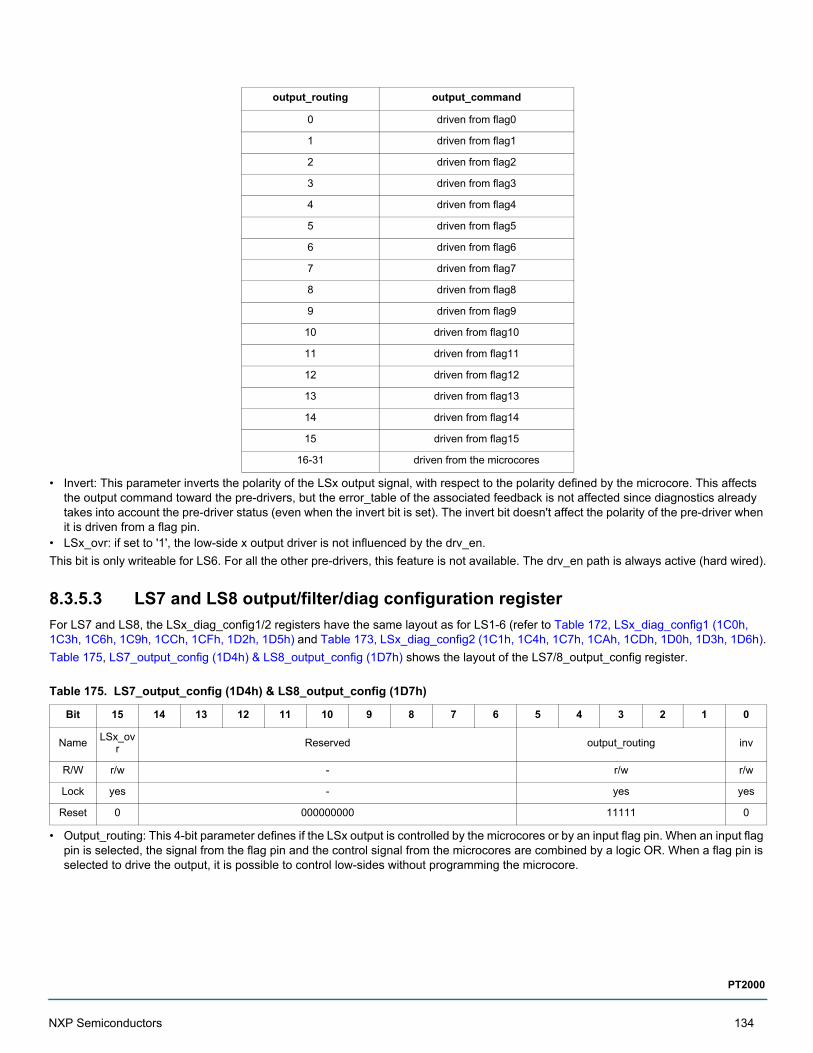
• Invert: This parameter inverts the polarity of the LSx output signal, with respect to the polarity defined by the microcore. This affects the output command toward the pre-drivers, but the error_table of the associated feedback is not affected since diagnostics already takes into account the pre-driver status (even when the invert bit is set). The invert bit doesn't affect the polarity of the pre-driver when it is driven from a flag pin.
• LSx_ovr: if set to '1', the low-side x output driver is not influenced by the drv_en.
This bit is only writeable for LS6. For all the other pre-drivers, this feature is not available. The drv_en path is always active (hard wired).
8.3.5.3 LS7 and LS8 output/filter/diag configuration register
For LS7 and LS8, the LSx_diag_config1/2 registers have the same layout as for LS1-6 (refer to Table 172, LSx_diag_config1 (1C0h, 1C3h, 1C6h, 1C9h, 1CCh, 1CFh, 1D2h, 1D5h) and Table 173, LSx_diag_config2 (1C1h, 1C4h, 1C7h, 1CAh, 1CDh, 1D0h, 1D3h, 1D6h).
Table 175, LS7_output_config (1D4h) & LS8_output_config (1D7h) shows the layout of the LS7/8_output_config register.
• Output_routing: This 4-bit parameter defines if the LSx output is controlled by the microcores or by an input flag pin. When an input flag pin is selected, the signal from the flag pin and the control signal from the microcores are combined by a logic OR. When a flag pin is selected to drive the output, it is possible to control low-sides without programming the microcore.
output_routing output_command
0 driven from flag0
1 driven from flag1
2 driven from flag2
3 driven from flag3
4 driven from flag4
5 driven from flag5
6 driven from flag6
7 driven from flag7
8 driven from flag8
9 driven from flag9
10 driven from flag10
11 driven from flag11
12 driven from flag12
13 driven from flag13
14 driven from flag14
15 driven from flag15
16-31 driven from the microcores
Table 175. LS7_output_config (1D4h) & LS8_output_config (1D7h)
Bit 15 14 13 12 11 10 9 8 7 6 5 4 3 2 1 0
NameLSx_ov
rReserved output_routing inv
R/W r/w - r/w r/w
Lock yes - yes yes
Reset 0 000000000 11111 0
NXP Semiconductors 134
PT2000
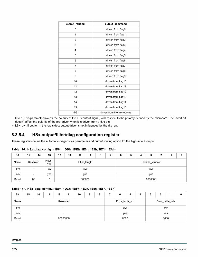
• Invert: This parameter inverts the polarity of the LSx output signal, with respect to the polarity defined by the microcore. The invert bit doesn't affect the polarity of the pre-driver when it is driven from a flag pin.
• LSx_ovr: if set to '1', the low-side x output driver is not influenced by the drv_en.
8.3.5.4 HSx output/filter/diag configuration register
These registers define the automatic diagnostics parameter and output routing option fro the high-side X output.
output_routing output_command
0 driven from flag0
1 driven from flag1
2 driven from flag2
3 driven from flag3
4 driven from flag4
5 driven from flag5
6 driven from flag6
7 driven from flag7
8 driven from flag8
9 driven from flag9
10 driven from flag10
11 driven from flag11
12 driven from flag12
13 driven from flag13
14 driven from flag14
15 driven from flag15
16-31 driven from the microcores
Table 176. HSx_diag_config1 (1D8h, 1DBh, 1DEh, 1E0h, 1E4h, 1E7h, 1EAh)
Bit 15 14 13 12 11 10 9 8 7 6 5 4 3 2 1 0
Name ReservedFilter_t
ypeFilter_length Disable_window
R/W - r/w r/w r/w
Lock - yes yes yes
Reset 00 0 000000 0000000
Table 177. HSx_diag_config2 (1D9h, 1DCh, 1DFh, 1E2h, 1E5h, 1E8h, 1EBh)
Bit 15 14 13 12 11 10 9 8 7 6 5 4 3 2 1 0
Name Reserved Error_table_src Error_table_vds
R/W - r/w r/w
Lock - yes yes
Reset 00000000 0000 0000
135 NXP Semiconductors
PT2000
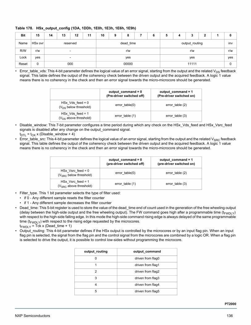
• Error_table_vds: This 4-bit parameter defines the logical value of an error signal, starting from the output and the related VDS feedback signal. This table defines the output of the coherency check between the driven output and the acquired feedback. A logic 1 value means there is no coherency in the check and then an error signal towards the micro-microcore should be generated.
• Disable_window: This 7-bit parameter configures a time period during which any check on the HSx_Vds_feed and HSx_Vsrc_feed signals is disabled after any change on the output_command signal. tDTL = tCK x (Disable_window + 4)
• Error_table_src: This 4-bit parameter defines the logical value of an error signal, starting from the output and the related VSRC feedback signal. This table defines the output of the coherency check between the driven output and the acquired feedback. A logic 1 value means there is no coherency in the check and then an error signal towards the micro-microcore should be generated.
• Filter_type. This 1 bit parameter selects the type of filter used:• if 0 - Any different sample resets the filter counter• if 1 - Any different sample decreases the filter counter
• Dead_time: This 5-bit register is used to store the value of the dead_time end of count used in the generation of the free wheeling output (delay between the high-side output and the free wheeling output). The FW command goes high after a programmable time (tFWDLY) with respect to the high-side falling edge. In this mode the high-side command rising edge is always delayed of the same programmable time (tFWDLY) with respect to the rising edge requested by the microcores. tFWDLY = Tck x (Dead_time + 1)
• Output_routing: This 4-bit parameter defines if the HSx output is controlled by the microcores or by an input flag pin. When an input flag pin is selected, the signal from the flag pin and the control signal from the microcores are combined by a logic OR. When a flag pin is selected to drive the output, it is possible to control low-sides without programming the microcore.
Table 178. HSx_output_config (1DA, 1DDh, 1E0h, 1E3h, 1E6h, 1E9h)
Bit 15 14 13 12 11 10 9 8 7 6 5 4 3 2 1 0
Name HSx ovr reserved dead_time output_routing inv
R/W r/w - r/w r/w r/w
Lock yes - yes yes yes
Reset 0 000 00000 11111 0
output_command = 0(Pre-driver switched off)
output_command = 1(Pre-driver switched on)
HSx_Vds_feed = 0(VDS below threshold)
error_table(0) error_table (2)
HSx_Vds_feed = 1(VDS above threshold)
error_table (1) error_table (3)
output_command = 0(pre-driver switched off)
output_command = 1(pre-driver switched on)
HSx_Vsrc_feed = 0(VSRC below threshold)
error_table(0) error_table (2)
HSx_Vsrc_feed = 1(VSRC above threshold)
error_table (1) error_table (3)
output_routing output_command
0 driven from flag0
1 driven from flag1
2 driven from flag2
3 driven from flag3
4 driven from flag4
5 driven from flag5
NXP Semiconductors 136
PT2000
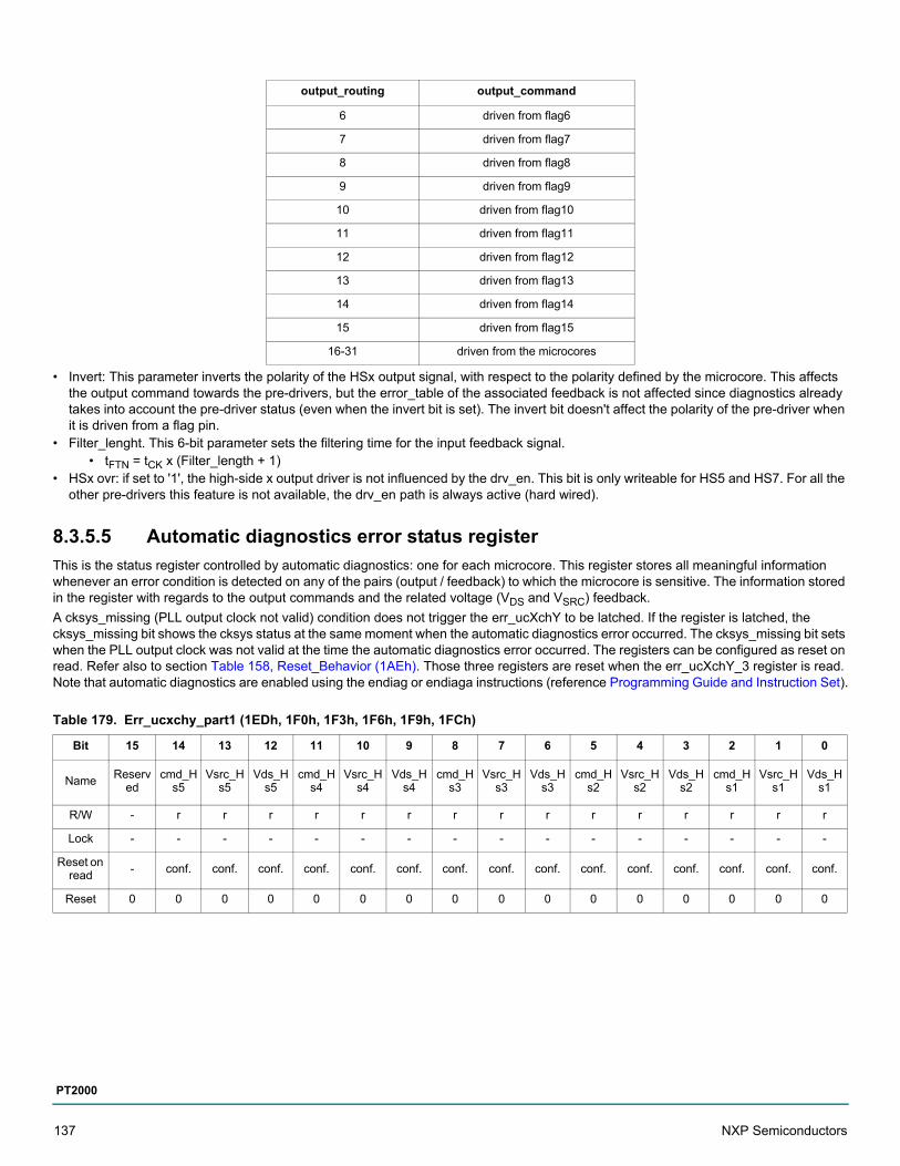
• Invert: This parameter inverts the polarity of the HSx output signal, with respect to the polarity defined by the microcore. This affects the output command towards the pre-drivers, but the error_table of the associated feedback is not affected since diagnostics already takes into account the pre-driver status (even when the invert bit is set). The invert bit doesn't affect the polarity of the pre-driver when it is driven from a flag pin.
• Filter_lenght. This 6-bit parameter sets the filtering time for the input feedback signal.• tFTN = tCK x (Filter_length + 1)
• HSx ovr: if set to '1', the high-side x output driver is not influenced by the drv_en. This bit is only writeable for HS5 and HS7. For all the other pre-drivers this feature is not available, the drv_en path is always active (hard wired).
8.3.5.5 Automatic diagnostics error status register
This is the status register controlled by automatic diagnostics: one for each microcore. This register stores all meaningful information whenever an error condition is detected on any of the pairs (output / feedback) to which the microcore is sensitive. The information stored in the register with regards to the output commands and the related voltage (VDS and VSRC) feedback.
A cksys_missing (PLL output clock not valid) condition does not trigger the err_ucXchY to be latched. If the register is latched, the cksys_missing bit shows the cksys status at the same moment when the automatic diagnostics error occurred. The cksys_missing bit sets when the PLL output clock was not valid at the time the automatic diagnostics error occurred. The registers can be configured as reset on read. Refer also to section Table 158, Reset_Behavior (1AEh). Those three registers are reset when the err_ucXchY_3 register is read. Note that automatic diagnostics are enabled using the endiag or endiaga instructions (reference Programming Guide and Instruction Set).
6 driven from flag6
7 driven from flag7
8 driven from flag8
9 driven from flag9
10 driven from flag10
11 driven from flag11
12 driven from flag12
13 driven from flag13
14 driven from flag14
15 driven from flag15
16-31 driven from the microcores
Table 179. Err_ucxchy_part1 (1EDh, 1F0h, 1F3h, 1F6h, 1F9h, 1FCh)
Bit 15 14 13 12 11 10 9 8 7 6 5 4 3 2 1 0
NameReserv
edcmd_H
s5Vsrc_H
s5Vds_H
s5cmd_H
s4Vsrc_H
s4Vds_H
s4cmd_H
s3Vsrc_H
s3Vds_H
s3cmd_H
s2Vsrc_H
s2Vds_H
s2cmd_H
s1Vsrc_H
s1Vds_H
s1
R/W - r r r r r r r r r r r r r r r
Lock - - - - - - - - - - - - - - - -
Reset on read
- conf. conf. conf. conf. conf. conf. conf. conf. conf. conf. conf. conf. conf. conf. conf.
Reset 0 0 0 0 0 0 0 0 0 0 0 0 0 0 0 0
output_routing output_command
137 NXP Semiconductors
PT2000
8.3.5.6 Automatic diagnostics command/feedback coherency
The PT2000 performs automatic diagnostics by checking the coherency between the commands it sends to the MOSFETs and the VDS/VSRC feedback it gets. The following register configure if the check is between:
• diag_option = 0 => coherency check between what the microcore wants to drive, using instructions like sto/stos/ldca/ldcd and the feedback from the MOSFETS
• diag_option = 1 => coherency check between what the device is really driving, using instructions like sto/stos/ldca/ldcd, but also including the status of overtemperature/drven pin/undervoltages/etc. and the feedback from the MOSFETS
For example, in case of an overtemperature/drven pin/undervoltages/etc., drivers are disabled:
In case of diag_option =0 =>, automatic diagnosis coherency check fails and detects an error (microcores are trying to drive but the output does not move due to a disabled driver, VDS/VSRC feedback incoherent with driving request => fail)
In case of diag_option =1 =>, automatic diagnosis coherency check does not detect anything (microcores are trying to drive, but the output does not move due to a disabled driver, VDS/VSRC feedback is in this case first compared to “no driving” => ok)
To summarize if the diag_option = 0 then automatic diagnostics is able to cover all kind of faults.
Table 180. Err_ucxchy_part2 (1EEh, 1F1h, 1F4h, 1F7h, 1FAh, 1FDh)
Bit 15 14 13 12 11 10 9 8 7 6 5 4 3 2 1 0
Namecksys_mi
ssingReserved
cmd_Hs7
Vsrc_Hs7
Vds_Hs7
cmd_Hs6
Vsrc_Hs6
Vds_Hs6
R/W r - r r r r r r
Lock - - - - - - - -
Reset on read
conf. - conf. conf. conf. conf. conf. conf.
Reset 0 000000000 0 0 0 0 0 0
Table 181. Err_ucxchy_part3 (1EFh, 1F2h, 1F5h, 1F8h, 1FBh, 1FEh)
Bit 15 14 13 12 11 10 9 8 7 6 5 4 3 2 1 0
Namecmd_L
S8Vds_Ls
8cmd_L
S7Vds_Ls
7cmd_L
s6Vds_Ls
6cmd_L
s5Vds_Ls
5cmd_L
s4Vds_Ls
4cmd_L
s3Vds_Ls
3cmd_L
s2Vds_Ls
2cmd_L
s1Vds_Ls
1
R/W r r r r r r r r r r r r r r r r
Lock - - - - - - - - - - - - - - - -
Reset on read
conf. conf. conf. conf. conf. conf. conf. conf. conf. conf. conf. conf. conf. conf. conf. conf.
Reset 0 0 0 0 0 0 0 0 0 0 0 0 0 0 0 0
Table 182. diagnostics_option register (1FFh)
Bit 15 14 13 12 11 10 9 8 7 6 5 4 3 2 1 0
Name ReservedDiag_opt
ion
R/W - r/w
Lock - yes
Reset 000000000000000 1
NXP Semiconductors 138
PT2000
9 Typical applications
The PT2000 can be configured in several applications. Figure 35 and Figure 36 shows the PT2000 in a typical application.
9.1 Application diagram: 3 bank, 6 cylinder with DC/DC
Figure 35. Example of application circuit (6 cylinder 3 bank with DC/DC)
B_
HS1
G_H
S1S_
HS1
B_HS
2G
_HS2
S_HS
2
D_L
S1G
_LS1
D_L
S2G
_LS2
VSEN
SE_P
1
VSEN
SE_N
1
B_HS
3G
_HS3
S_HS
3
B_HS
4G
_HS4
S_HS
4
D_L
S3G
_LS3
D_L
S4G
_LS4 B_HS7
G_HS7
S_HS7
MC3
3PT2
000
6 Cy
linde
r3
Bank
D_LS8G_LS8
VSEN
SE_P
2
VSEN
SE_N
2
VSENSE_P3
VSENSE_N3
VBAT
VCCP
VCC2P5
VCC5
VCCIO
AGNDDGNDPGND
VBO
OST
G_L
S7
VSEN
SE_N
5
VSEN
SE_P
5
D_L
S7
B_
HS5
G_H
S5S_
HS5
B_HS
6G
_HS6
S_HS
6
D_L
S5G
_LS5
D_L
S6G
_LS6
VSEN
SE_P
6
VSEN
SE_N
6
START1
START2
START3
START4
START5
START6
START7
CSB
MISO
MOSI
SCKL
DRVEN
RESET
CLK
IRQB
FLAG0
FLAG1
FLAG2
FLAG3DBG
To M
CU e
TPU
To M
CU S
PITo
MCU
IOs
To M
CU IO
s (o
ptio
nal)
INJECTOR2
INJECTOR1
INJECTOR4
INJECTOR3
PUMP
INJECTOR5
INJECTOR6
DC/D
C
BAN
K3BA
NK1
PUM
P
M
Supp
lies
BAN
K2
OA_
3
OA_
1
OA_
2
MCU
ADC
MCU
ADC
MCU ADC
VPW
R
VPW
R
VPW
R
VPW
R
VPW
R
VPW
R33
0Ω
330Ω
330Ω
330Ω
330Ω
33
0Ω
330Ω
330Ω
330Ω
330Ω
330Ω
330Ω
330Ω
330Ω
33
0Ω
100n
F
100n
F
100n
F
100n
F
100nF
100n
F
100n
F
100n
F
100n
F
100n
F
100n
F47
0μF
470μ
F6μH
220n
F4.
7nF
5.1Ω
10μH
10m
Ω
15m
Ω
15m
Ω 15
mΩ
15m
Ω
4.7n
F
4.7n
F
4.7n
F
4.7n
F
4.7n
F
4.7n
F 4.7n
F
4.7n
F
4.7n
F
4.7n
F4.
7nF
4.7n
F
4.7n
F
4.7n
F
4.7n
F
4.7n
F4.
7nF
4.7n
F
4.7n
F
4.7n
F
4.7n
F
4.7n
F
4.7n
F
4.7n
F4.
7nF
4.7n
F4.
7nF
330p
F
330p
F
330p
F
680μ
F
100n
F
1μH
1μH
100n
F
330p
F
330p
F
VBoo
st
VBoo
stVB
oostVB
oost
VBoo
st VBoo
stVB
oost
VBoo
st VBoo
stVB
oost
330p
F
139 NXP Semiconductors
PT2000

9.2 Application diagram: 3 bank, 3 cylinder (full overlap) with DC/DC
Figure 36. Application diagram 3 bank, 3 cylinder with synchronous rectification and DC/DC
B_
HS1
G_H
S1S_
HS1
B_HS
2G
_HS2
S_HS
2
D_L
S1G
_LS1
D_L
S2G
_LS2
VSEN
SE_P
1
VSEN
SE_N
1
B_HS
3G
_HS3
S_HS
3
B_HS
4G
_HS4
S_HS
4
D_L
S3G
_LS3
D_L
S4G
_LS4 B_HS7
G_HS7
S_HS7
MC3
3PT2
000
3 Cy
linde
r3
Bank
D_LS8G_LS8
VSEN
SE_P
2
VSEN
SE_N
2VSENSE_P3
VSENSE_N3
VBAT
VCCP
VCC2P5
VCC5
VCCIO
AGNDDGNDPGND
VBO
OST
G_L
S7
VSEN
SE_N
5
VSEN
SE_P
5
D_L
S7
START1
START2
START3
START4
START5
START6
START7
CSB
MISO
MOSI
SCKL
DRVEN
RESET
CLK
IRQB
FLAG0
FLAG1
FLAG2
FLAG3DBG
To M
CU e
TPU
To M
CU S
PITo
MCU
IOs
To M
CU IO
s (o
ptio
nal)
INJECTOR1INJECTOR2
PUMP
DC/D
C
BAN
K1
PUM
P
M
Supp
lies
BAN
K2
OA_
1
OA_
2
MCU
ADC
MCU ADC
VPW
R
VPW
R
VPW
R
VPW
R
VPW
R
330Ω
33
0Ω
330Ω
330Ω
330Ω
33
0Ω
330Ω
330Ω
330Ω
330Ω
330Ω
100n
F
100n
F
100n
F
100n
F
100nF
100n
F
100n
F
100n
F
100n
F47
0μF
470μ
F6μH
220n
F4.
7nF
5.1Ω
10μH
10m
Ω
15m
Ω
15m
Ω
15m
Ω
4.7n
F
4.7n
F
4.7n
F
4.7n
F
4.7n
F
4.7n
F
4.7n
F
4.7n
F
4.7n
F
4.7n
F
4.7n
F
4.7n
F
4.7n
F
330p
F
330p
F
680μ
F
100n
F
1μH
1μH
100n
F
330p
F
330p
F
VBoo
st
VBoo
st
VBoo
st
VBoo
st
VBoo
st
330p
F
4.
7nF
FW1
4.7n
F
FW2
B_
HS5
G_H
S5S_
HS5
B_HS
6G
_HS6
S_HS
6
D_L
S5G
_LS5
D_L
S6G
_LS6
VSEN
SE_P
6
VSEN
SE_N
6
INJECTOR3
BAN
K3
OA_
3M
CU A
DC
VPW
R
330Ω
330Ω
330Ω
33
0Ω
100n
F
100n
F
15m
Ω
4.7n
F4.7n
F
4.7n
F
4.7n
F
4.7n
F
330p
F
VBoo
st
VBoo
st FW3
4.7n
F
NXP Semiconductors 140
PT2000
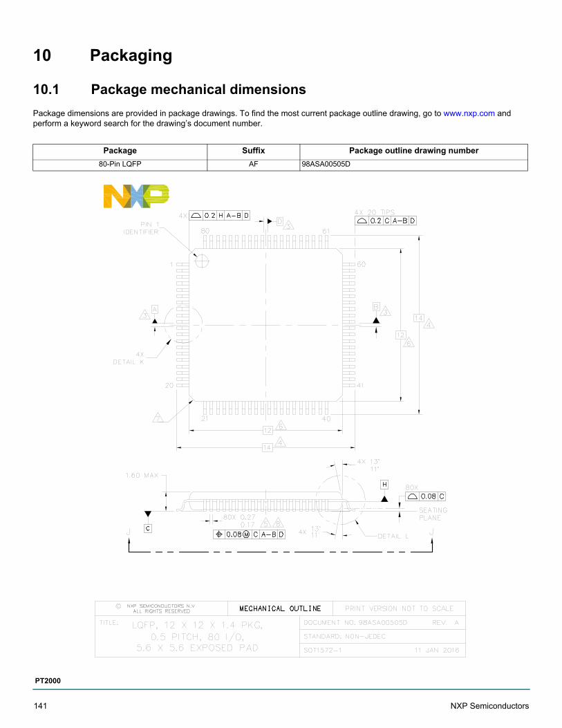
10 Packaging
10.1 Package mechanical dimensions
Package dimensions are provided in package drawings. To find the most current package outline drawing, go to www.nxp.com and perform a keyword search for the drawing’s document number.
Package Suffix Package outline drawing number
80-Pin LQFP AF 98ASA00505D
141 NXP Semiconductors
PT2000
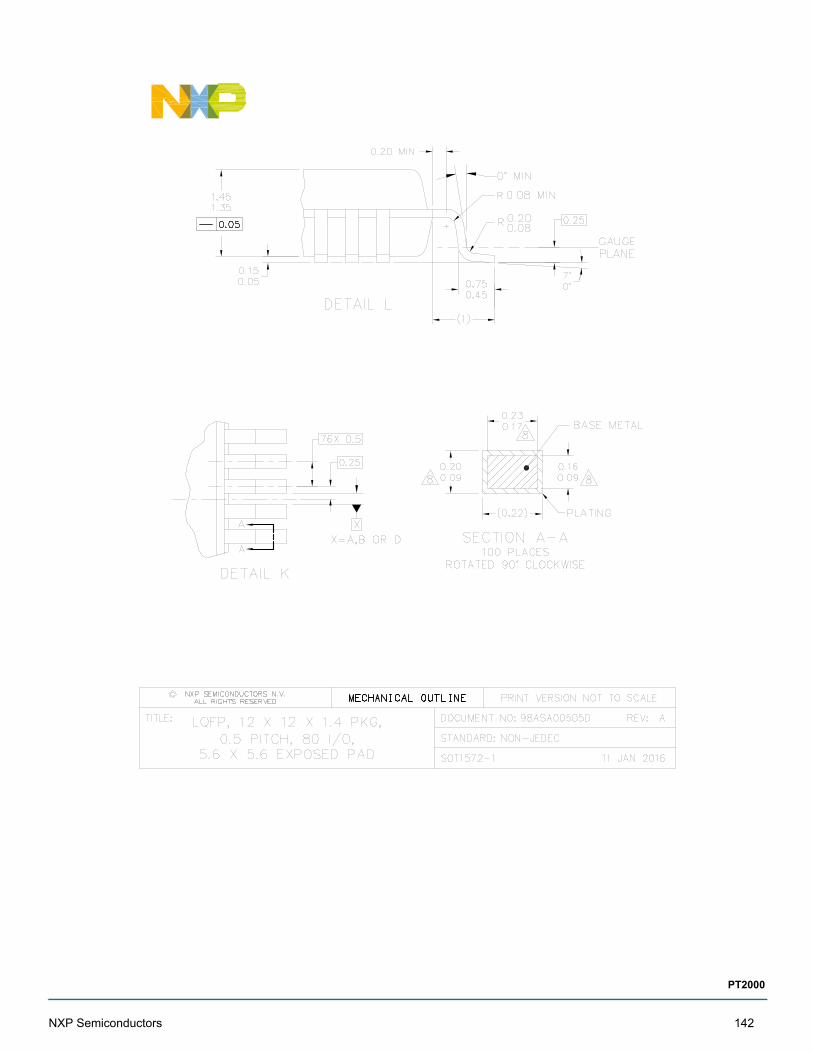
NXP Semiconductors 142
PT2000
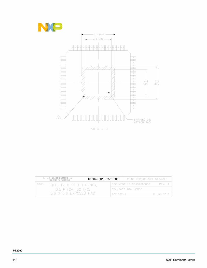
143 NXP Semiconductors
PT2000
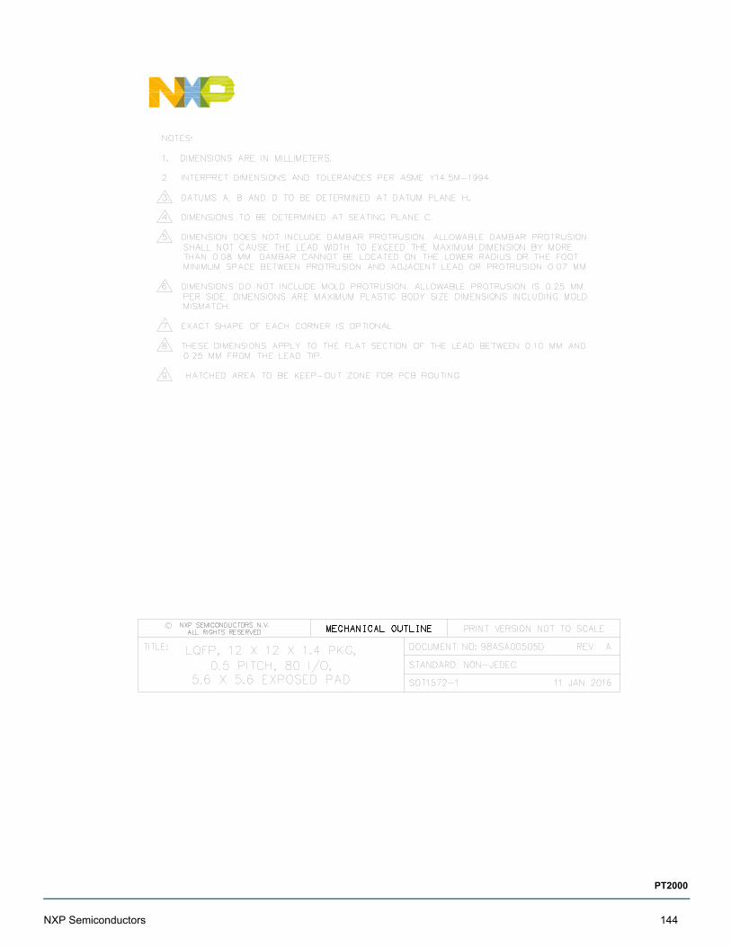
NXP Semiconductors 144
PT2000
11 Reference section
Table 183. PT2000 reference
Description URL
Programming guide and instruction set http://www.nxp.com/files/analog/doc/user_guide/PT2000SWUG.pdf
Product summary page http://www.nxp.com/webapp/sps/site/prod_summary.jsp?code=PT2000
145 NXP Semiconductors
PT2000
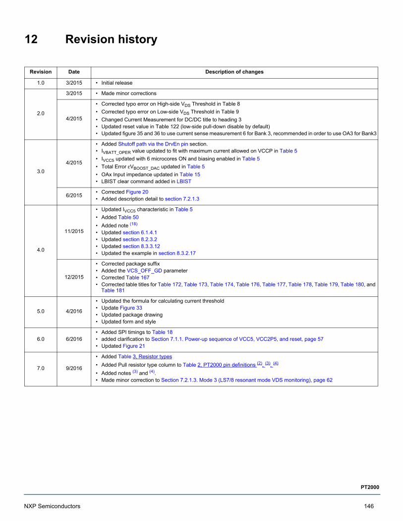
12 Revision history
Revision Date Description of changes
1.0 3/2015 • Initial release
2.0
3/2015 • Made minor corrections
4/2015
• Corrected typo error on High-side VDS Threshold in Table 8
• Corrected typo error on Low-side VDS Threshold in Table 9
• Changed Current Measurement for DC/DC title to heading 3• Updated reset value in Table 122 (low-side pull-down disable by default)• Updated figure 35 and 36 to use current sense measurement 6 for Bank 3, recommended in order to use OA3 for Bank3
3.0
4/2015
• Added Shutoff path via the DrvEn pin section.• IVBATT_OPER value updated to fit with maximum current allowed on VCCP in Table 5
• IVCC5 updated with 6 microcores ON and biasing enabled in Table 5
• Total Error εVBOOST_DAC updated in Table 5
• OAx Input impedance updated in Table 15• LBIST clear command added in LBIST
6/2015• Corrected Figure 20• Added description detail to section 7.2.1.3
4.0
11/2015
• Updated IVCC5 characteristic in Table 5
• Added Table 50
• Added note (18)
• Updated section 6.1.4.1• Updated section 8.2.3.2• Updated section 8.3.3.12• Updated the example in section 8.3.2.17
12/2015
• Corrected package suffix• Added the VCS_OFF_GD parameter• Corrected Table 167• Corrected table titles for Table 172, Table 173, Table 174, Table 176, Table 177, Table 178, Table 179, Table 180, and
Table 181
5.0 4/2016
• Updated the formula for calculating current threshold• Update Figure 33• Updated package drawing• Updated form and style
6.0 6/2016• Added SPI timings to Table 18• added clarification to Section 7.1.1. Power-up sequence of VCC5, VCC2P5, and reset, page 57• Updated Figure 21
7.0 9/2016
• Added Table 3, Resistor types
• Added Pull resistor type column to Table 2, PT2000 pin definitions (2), (3), (4)
• Added notes (3) and (4).• Made minor correction to Section 7.2.1.3. Mode 3 (LS7/8 resonant mode VDS monitoring), page 62
NXP Semiconductors 146
PT2000
Information in this document is provided solely to enable system and software implementers to use NXP products.
There are no expressed or implied copyright licenses granted hereunder to design or fabricate any integrated circuits
based on the information in this document. NXP reserves the right to make changes without further notice to any
products herein.
NXP makes no warranty, representation, or guarantee regarding the suitability of its products for any particular
purpose, nor does NXP assume any liability arising out of the application or use of any product or circuit, and
specifically disclaims any and all liability, including without limitation, consequential or incidental damages. "Typical"
parameters that may be provided in NXP data sheets and/or specifications can and do vary in different applications,
and actual performance may vary over time. All operating parameters, including "typicals," must be validated for each
customer application by the customer's technical experts. NXP does not convey any license under its patent rights nor
the rights of others. NXP sells products pursuant to standard terms and conditions of sale, which can be found at the
following address:
http://www.nxp.com/terms-of-use.html.
How to Reach Us:Home Page: NXP.com
Web Support: http://www.nxp.com/support
NXP, the NXP logo, Freescale, the Freescale logo and SMARTMOS are trademarks of NXP B.V. All other product or
service names are the property of their respective owners. All rights reserved.
© 2016 NXP B.V.
Document Number: MC33PT2000Rev. 7.0
9/2016