Embed Size (px)
Citation preview
NVTP1001 – Technical Reference Manual
NVTP1001 Telecom cPCI Module PCB Rev. 1.2 Technical Reference Manual V1.9

NVTP1001 – Technical Reference Manual
The NVTP1001 has been designed by:
N.A.T. GmbH Kamillenweg 22
D-53757 Sankt Augustin
Phone: ++49/2241/3989-0 Fax: ++49/2241/3989-10
E-Mail: [email protected]
Internet: http://www.nateurope.com
Version 1.9 © N.A.T. GmbH 2
NVTP1001 – Technical Reference Manual
Disclaimer
The following documentation, compiled by N.A.T. GmbH (henceforth called N.A.T.), repre-sents the current status of the product´s development. The documentation is updated on a regular basis. Any changes which might ensue, including those necessitated by updated speci-fications, are considered in the latest version of this documentation. N.A.T. is under no obli-gation to notify any person, organization, or institution of such changes or to make these changes public in any other way. We must caution you, that this publication could include technical inaccuracies or typographi-cal errors. N.A.T. offers no warranty, either expressed or implied, for the contents of this documentation or for the product described therein, including but not limited to the warranties of merchant-ability or the fitness of the product for any specific purpose. In no event will N.A.T. be liable for any loss of data or for errors in data utilization or processing resulting from the use of this product or the documentation. In particular, N.A.T. will not be responsible for any direct or indirect damages (including lost profits, lost savings, delays or interruptions in the flow of business activities, including but not limited to, special, incidental, consequential, or other similar damages) arising out of the use of or inability to use this product or the associated documentation, even if N.A.T. or any authorized N.A.T. representative has been advised of the possibility of such damages. The use of registered names, trademarks, etc. in this publication does not imply, even in the absence of a specific statement, that such names are exempt from the relevant protective laws and regulations (patent laws, trade mark laws, etc.) and therefore free for general use. In no case does N.A.T. guarantee that the information given in this documentation is free of such third-party rights. Neither this documentation nor any part thereof may be copied, translated, or reduced to any electronic medium or machine form without the prior written consent from N.A.T. GmbH. This product (and the associated documentation) is governed by the N.A.T. General Conditions and Terms of Delivery and Payment.
Note: The release of the Hardware Manual is relatedto a certain HW board revision given in thedocument title. For HW revisions earlier thanthe one given in the document title pleasecontact N.A.T. for the corresponding olderHardware Manual release.
Version 1.9 © N.A.T. GmbH 3
NVTP1001 – Technical Reference Manual
Table of Contents TABLE OF CONTENTS...................................................................................................................................... 4
LIST OF TABLES ................................................................................................................................................ 8
LIST OF FIGURES ............................................................................................................................................ 10
CONVENTIONS................................................................................................................................................. 11
1 INTRODUCTION ..................................................................................................................................... 12 1.1 BOARD FEATURES .............................................................................................................................. 15 1.2 BOARD SPECIFICATION ....................................................................................................................... 17
2 INSTALLATION ...................................................................................................................................... 18 2.1 SAFETY NOTE ..................................................................................................................................... 18 2.2 INSTALLATION PREREQUISITES AND REQUIREMENTS ......................................................................... 19
2.2.1 Requirements................................................................................................................................. 19 2.2.2 Power supply................................................................................................................................. 19 2.2.3 Automatic Power Up ..................................................................................................................... 20
2.3 STATEMENT ON ENVIRONMENTAL PROTECTION................................................................................. 21 2.3.1 Compliance to RoHS Directive ..................................................................................................... 21 2.3.2 Compliance to WEEE Directive .................................................................................................... 21 2.3.3 Compliance to CE Directive ......................................................................................................... 22 2.3.4 Product Safety ............................................................................................................................... 22
3 LOCATION OVERVIEW........................................................................................................................ 23
4 FUNCTIONAL BLOCKS......................................................................................................................... 24 4.1 PROCESSOR......................................................................................................................................... 24 4.2 MEMORY ............................................................................................................................................ 25
4.2.1 SDRAM.......................................................................................................................................... 25 4.2.2 FLASH........................................................................................................................................... 26
4.2.2.1 Main FLASH memory......................................................................................................................... 26 4.2.2.2 Fallback FLASH memory ................................................................................................................... 26
4.2.3 EEPROM....................................................................................................................................... 26 4.2.3.1 I2C Devices.......................................................................................................................................... 26 4.2.3.2 Microwire Devices .............................................................................................................................. 26
4.3 TDM BUS AND H.110 BUS CONTROLLER ........................................................................................... 27 4.4 ETHERNET .......................................................................................................................................... 28
4.4.1 Front Panel Gigabit Ethernet........................................................................................................ 28 4.4.2 Backplane 100BaseT Ethernet ..................................................................................................... 28
4.5 RS232 INTERFACES ............................................................................................................................ 28 4.6 FRONT PANEL ELEMENTS ................................................................................................................... 29
5 HARDWARE............................................................................................................................................. 30 5.1 MEMORY MAP (CPU)......................................................................................................................... 30 5.2 MEMORY MAP (PCI) .......................................................................................................................... 31 5.3 DEFINITION OF POWERQUICC II PORT PINS...................................................................................... 32 5.4 CPU - PLL-SETUP.............................................................................................................................. 36 5.5 INTERRUPT STRUCTURE...................................................................................................................... 36
Version 1.9 © N.A.T. GmbH 4
NVTP1001 – Technical Reference Manual
5.6 RESET STRATEGY .............................................................................................................................. 38 5.6.1 CPU Reset Sources ....................................................................................................................... 41 5.6.2 CPU Reset Pins ............................................................................................................................. 42 5.6.3 Reset of the PCI Buses ................................................................................................................. 42
5.7 ARBITRATION OF THE INTERNAL BUSES.............................................................................................. 43 5.7.1 PCI bus 1....................................................................................................................................... 43 5.7.2 PCI bus 2....................................................................................................................................... 43 5.7.3 60x bus .......................................................................................................................................... 43
5.8 SLOT 1 FUNCTIONALITY ..................................................................................................................... 44 5.8.1 Compact PCI Bus Arbitration ....................................................................................................... 44 5.8.2 Compact PCI Bus Clocks .............................................................................................................. 44
5.9 HOT SWAP CAPABILITY ...................................................................................................................... 45 5.10 IPMI INTERFACE ................................................................................................................................ 45 5.11 DEVICE CONFIGURATION.................................................................................................................... 46
5.11.1 Onboard PCI devices ............................................................................................................... 46 5.11.2 MPC8280 CPU......................................................................................................................... 46 U
5.12 MINIBRIDGES...................................................................................................................................... 47 5.12.1 Minibridge of the i21555 PCI Bridge....................................................................................... 47 5.12.2 Minibridge of the i82545 Gigabit Ethernet Controller ............................................................ 47 5.12.3 Minibridges of the AM79C973 Ethernet Controllers ............................................................... 47 5.12.4 Minibridge of the T8110 H.110 TSI Controller........................................................................ 47
5.13 STATUS / CONTROL REGISTERS .......................................................................................................... 48 5.13.1 Board Hardware Revision Status Register ............................................................................... 49 5.13.2 Interrupt Status Register 1........................................................................................................ 49 5.13.3 Interrupt Status Register 2........................................................................................................ 50 5.13.4 Interrupt Status Register 3........................................................................................................ 50 5.13.5 Interrupt Enable Register 1 ...................................................................................................... 51 5.13.6 Interrupt Enable Register 2 ...................................................................................................... 51 5.13.7 Interrupt Enable Register 3 ...................................................................................................... 52 5.13.8 RESET Control / Status Register .............................................................................................. 52
5.13.8.1 Software RESET to CPU and Peripherals ........................................................................................... 52 5.13.8.2 Software RESET to CPU only............................................................................................................. 53 5.13.8.3 Software RESET to PMC slots 1 and 2 ............................................................................................... 53 5.13.8.4 Software RESET to cPCI Bus only ..................................................................................................... 53
5.13.9 Status Register 1....................................................................................................................... 54 5.13.10 Status Register 2....................................................................................................................... 54 5.13.11 Status Register 3....................................................................................................................... 55 5.13.12 Control / Status Register 4 ....................................................................................................... 55 5.13.13 Control / Status Register 5 ....................................................................................................... 56 5.13.14 Control / Status Register 6 ....................................................................................................... 56
5.13.14.1 SDRAM Configuration Pins................................................................................................................ 57 5.13.14.2 I2C Interface Pins................................................................................................................................. 57
5.13.15 Control / Status Register 7 ....................................................................................................... 58 5.13.16 Control / Status Register 8 ....................................................................................................... 58
5.14 PORT PIN ASSIGNMENT OF THE PERIPHERAL DEVICES........................................................................ 59 5.14.1 Port Pins Assignment of the i82545 Gigabit Ethernet Controller ............................................ 59 5.14.2 Port Pins of the T8110 H.110 TSI Controller........................................................................... 59 5.14.3 Port Pins of the PCI 6150 PCI PCI Bridge ......................................................................... 60
6 CONNECTORS......................................................................................................................................... 61 6.1 CONNECTOR AND JUMPER OVERVIEW ................................................................................................ 61 6.2 CONNECTOR JP1: BDM AND JTAG CONNECTOR ............................................................................... 62 6.3 CONNECTOR JP2: FRONT PANEL EJECTOR SWITCH ............................................................................ 62 6.4 CONNECTOR JP3: JTAG CHAIN OF ONBOARD DEVICES...................................................................... 63 6.5 CONNECTOR JP4: CPLD PROGRAMMING PORT.................................................................................. 63 6.6 CONNECTOR JP5: IPMI PORT............................................................................................................. 64 6.7 JUMPER JP6: CORE DISABLE JUMPER ................................................................................................. 64 6.8 JUMPER JP7: BOOT FLASH SELECT JUMPER .................................................................................... 64
Version 1.9 © N.A.T. GmbH 5
NVTP1001 – Technical Reference Manual
6.9 CONNECTOR JP8: CENTRAL SWITCHING DEVICE PROGRAMMING PORT............................................. 65 6.10 CONNECTOR JP9: SECOND RS232 INTERFACE ................................................................................... 65 6.11 PMC SLOT 1 CONNECTORS ................................................................................................................ 66
6.11.1 PMC Slot 1 Connector P11 ...................................................................................................... 66 6.11.2 PMC Slot 1 Connector P12 ...................................................................................................... 67 6.11.3 PMC Slot 1 Connector P13 ...................................................................................................... 68 6.11.4 PMC Slot 1 Connector P14 ( PMC 1 I/O )............................................................................. 69 6.11.5 PMC Slot 2 Connector P21 ...................................................................................................... 70 6.11.6 PMC Slot 2 Connector P22 ...................................................................................................... 71 6.11.7 PMC Slot 2 Connector P23 ...................................................................................................... 72 6.11.8 PMC Slot 2 Connector P24 ( PMC 2 I/O )............................................................................. 73
6.12 COMPACT PCI BACKPLANE CONNECTORS ......................................................................................... 74 6.12.1 Compact PCI Backplane Connector J1.................................................................................... 74 6.12.2 Compact PCI Backplane Connector J2.................................................................................... 76 6.12.3 Compact PCI Backplane Connector J3.................................................................................... 78 6.12.4 Compact PCI Backplane Connector J4.................................................................................... 80
6.13 THE FRONT PANEL CONNECTORS ....................................................................................................... 82 6.13.1 Front Panel Connector J5 ........................................................................................................ 82 6.13.2 Front Panel Connector S1........................................................................................................ 82
7 NVTP1001 PROGRAMMING NOTES .................................................................................................. 83 7.1 MPC8280 HARD RESET CONFIGURATION WORD............................................................................... 83
7.1.1 Core Enabled Mode (default)........................................................................................................ 83 7.1.2 Core Disabled Mode (FLASH programming mode) ..................................................................... 84
7.2 RECOMMENDED GENERAL CONTROL REGISTER SETUP ...................................................................... 85 7.2.1 Register-Setup of the System Clock Control Register (SCCR) ...................................................... 85 7.2.2 Register-Setup of the System Protection Control Register (SYPCR)............................................. 85 7.2.3 Register-Setup of the Bus Configurations Register (BCR) ............................................................ 85 7.2.4 Register-Setup of the 60x Bus Arbiter Configurations Register (PPC_ACR) ............................... 86 7.2.5 Register-Setup of the Local Bus Arbiter Configurations Register (LCL_ACR) ............................ 86 7.2.6 Register-Setup of the SIU Module Configurations Register (SIUMCR)........................................ 86 7.2.7 Register-Setup of the 60x Bus Transfer Status/Control Register (TESCR1) ................................. 87 7.2.8 Register-Setup of the Local Bus Transfer Status/Control Register (L_TESCR1).......................... 87
7.3 RECOMMENDED REGISTER SETUP OF THE MEMORY CONTROLLER: ................................................... 88 7.3.1 Base Registers BRx: ...................................................................................................................... 88 7.3.2 Option Registers ORx.................................................................................................................... 91 7.3.3 Configuration for SDRAM Register Setup .................................................................................... 94 7.3.4 SDRAM Mode Register PSDMRx.................................................................................................. 95 7.3.5 PSRT 60x Bus-Assigned SDRAM Refresh Timer Register ............................................................ 95 7.3.6 MPTPR Memory Refresh Timer Prescaler Register ..................................................................... 95 7.3.7 UPM Machine Mode Register MxMR ........................................................................................... 95
7.4 SETUP OF THE SERIAL INTERFACES..................................................................................................... 96 7.4.1 RS232 Interface on the Front Panel Connector S1 ....................................................................... 96 7.4.2 RS232 Debug Interface on JP9 ..................................................................................................... 96 7.4.3 I2C Interface .................................................................................................................................. 96
7.5 DEFINITION OF THE MULTI-FUNCTION PINS ....................................................................................... 97 7.6 PROGRAMMING THE PCI BRIDGES...................................................................................................... 98
7.6.1 Intel 21555 Bridge Programming ................................................................................................. 98 7.6.1.1 Intel 21555 Power-Up Configuration .................................................................................................. 98 7.6.1.2 Configuration by EEPROM Load ....................................................................................................... 98
7.7 PROGRAMMING THE ETHERNET CONTROLLERS .................................................................................. 99 7.7.1 Intel 82545 Gigabit Ethernet Controller....................................................................................... 99 7.7.2 AMD 79C973 10/100 MBit Ethernet Controllers.......................................................................... 99
7.8 PROGRAMMING THE H.110 TSI CONTROLLER.................................................................................. 100 7.9 PROGRAMMING THE CENTRAL SWITCHING RESOURCE..................................................................... 101
7.9.1 Commonly used FPGA Sample Applications for TDM Bus ........................................................ 101 7.9.2 Simple TDM Interconnect Application........................................................................................ 102 7.9.3 Programmable TDM Interconnect Application........................................................................... 105
Version 1.9 © N.A.T. GmbH 6
NVTP1001 – Technical Reference Manual
7.9.3.1 The FPGA SPI Interface.................................................................................................................... 105 7.9.3.2 FPGA SPI Register Description ........................................................................................................ 105 7.9.3.3 FPGA SPI Register Overview ........................................................................................................... 106 7.9.3.4 TDM Register Description ................................................................................................................ 108
7.9.3.4.1 TDM Data Path Registers ............................................................................................................ 108 7.9.3.4.2 TDM data path Control / Status Registers.................................................................................... 109 7.9.3.4.3 Clock / Sync Control / Status Registers ....................................................................................... 110
7.9.3.5 SYNC to LREF Routing.................................................................................................................... 114 7.9.3.6 IPMI Register Description................................................................................................................. 117
7.9.3.6.1 IPMI Data Path Control............................................................................................................... 117 7.9.3.6.2 IPMI Data Path Control / Status Registers .................................................................................. 118
7.9.3.7 FPGA Revision Code Register .......................................................................................................... 122 7.9.4 TDM / I/O-Signal Routing to the Central Switching Resource ................................................... 123
8 KNOWN BUGS AND RESTRICTIONS............................................................................................... 131
APPENDIX A: REFERENCE DOCUMENTATION.................................................................................... 132
APPENDIX B: DOCUMENT’S HISTORY.................................................................................................... 133
Version 1.9 © N.A.T. GmbH 7
NVTP1001 – Technical Reference Manual
List of Tables Table 1: List of used abbreviations .................................................................................... 11 Table 2: NVTP1001 Features............................................................................................. 17 Table 3: Memory Map........................................................................................................ 30 Table 4: IDSEL Routing for internal PCI Bus 1 ................................................................ 31 Table 5: IDSEL Routing for internal PCI Bus 2 ................................................................ 31 Table 6: PowerQUICC II Port Pin Usage (Port A) ............................................................ 32 Table 7: PowerQUICC II Port Pin Usage (Port B)............................................................. 33 Table 8: PowerQUICC II Port Pin Usage (Port C)............................................................. 34 Table 9: PowerQUICC II Port Pin Usage (Port D) ............................................................ 35 Table 10: Interrupt Structure ................................................................................................ 36 Table 11: Reset Strategy, System Host Configuration........................................................ 39 Table 12: Reset Strategy, Peripheral Board Configuration ................................................. 40 Table 13: Status/Control Register Set .................................................................................. 48 Table 14: Board Hardware Revision Status Register ........................................................... 49 Table 15: Interrupt Status Register 1.................................................................................... 49 Table 16: Interrupt Status Register 2.................................................................................... 50 Table 17: Interrupt Status Register 3.................................................................................... 50 Table 18: Interrupt Enable Register 1 .................................................................................. 51 Table 19: Interrupt Enable Register 2 .................................................................................. 51 Table 20: Interrupt Enable Register 3 .................................................................................. 52 Table 21: RESET Control / Status Register ......................................................................... 52 Table 22: Status Register 1................................................................................................... 54 Table 23: Status Register 2................................................................................................... 54 Table 24: Status Register 3................................................................................................... 55 Table 25: Control / Status Register 4 ................................................................................... 55 Table 26: Control / Status Register 5 ................................................................................... 56 Table 27: Control / Status Register 6 ................................................................................... 56 Table 28: Supported SDRAM SODIMM Module Types..................................................... 57 Table 29: BNKSELx Programming ..................................................................................... 57 Table 30: Control / Status Register 7 ................................................................................... 58 Table 31: Control / Status Register 8 ................................................................................... 58 Table 32: Port Pins of the i82545 Gigabit Ethernet Controller ............................................ 59 Table 33: Port Pins of the T8110 TSI Controller ................................................................. 59 Table 34: PLX PCI 6150 Port Pin Usage ............................................................................. 60 Table 35: Development Port / BDM and IEEE 1149.1 Connector Pinout........................... 62 Table 36: Front Panel Ejector Switch................................................................................... 62 Table 37: JTAG Chain of onboard Devices ......................................................................... 63 Table 38: Lattice Programming Port .................................................................................... 63 Table 39: IPMI Port.............................................................................................................. 64 Table 40: Altera Programming Port ..................................................................................... 65 Table 41: Pin Assignment of the Second RS232 Interface .................................................. 65 Table 42: PMC Slot 1 Connector P11 .................................................................................. 66 Table 43: PMC Slot 1 Connector P12 .................................................................................. 67 Table 44: PMC Slot 1 Connector P13 .................................................................................. 68
Version 1.9 © N.A.T. GmbH 8
NVTP1001 – Technical Reference Manual
Table 45: PMC Slot 1 Connector P14 .................................................................................. 69 Table 46: PMC Slot 2 Connector P21 .................................................................................. 70 Table 47: PMC Slot 2 Connector P22 .................................................................................. 71 Table 48: PMC Slot 2 Connector P23 .................................................................................. 72 Table 49: PMC Slot 2 Connector P24 .................................................................................. 73 Table 50: Compact PCI Backplane Connector J1 Rows A – C ........................................... 74 Table 51: Compact PCI Backplane Connector J1 Rows D – F............................................ 75 Table 52: Compact PCI Backplane Connector J2 Rows A – C ........................................... 76 Table 53: Compact PCI Backplane Connector J2 Rows D – F............................................ 77 Table 54: Compact PCI Backplane Connector J3 Rows A – C ........................................... 78 Table 55: Compact PCI Backplane Connector J3 Rows D – F............................................ 79 Table 56: Compact PCI Backplane Connector J4 Rows A – C ........................................... 80 Table 57: Compact PCI Backplane Connector J4 Rows D – F............................................ 81 Table 58: Pin Assignment of the Front-panel Connector J5 (1000BaseT) .......................... 82 Table 59: Pin Assignment of the Front-panel Connector S1 (RS232) ................................. 82 Table 60: Hard Reset Configuration Word (as read from CPLD)........................................ 83 Table 61: Definition of the Multi-Function Pins.................................................................. 97 Table 62: Intel 21555 Power-Up Configuration................................................................... 98 Table 63: i21555 EEPROM Configuration .......................................................................... 98 Table 64: i82545 EEPROM Configuration .......................................................................... 99 Table 65: FPGA SPI Register Overview............................................................................ 106 Table 66: Multiplexer Inputs and their Hexadecimal Encoding ........................................ 108 Table 67: TDM data path Control / Status Registers, SPI Addresses 0x0 – 0x19 ............. 109 Table 68: Clock / Sync Control Register PQ2 MCC1, SPI Address 0x1a ......................... 110 Table 69: Clock / Sync Control Register PQ2 MCC2, SPI Address 0x1b......................... 111 Table 70: H.110 Clock / Sync Control Register PMC1, SPI Address 0x1c....................... 112 Table 71: SCbus Clock / Sync Control Register PMC1, SPI Address 0x1d...................... 112 Table 72: H.110 Clock / Sync Control Register PMC2, SPI Address 0x1e....................... 113 Table 73: SCbus Clock / Sync Control Register PMC2, SPI Address 0x1f....................... 113 Table 74: LREF Select Register 1, SPI Address 0x20 ....................................................... 114 Table 75: LREF Routing between PMC Sync Signals and T8110 TSI LREFs ................. 114 Table 76: LREF Select Register 2, SPI Address 0x21 ....................................................... 115 Table 77: LREF Select Register 3, SPI Address 0x22 ....................................................... 115 Table 78: LREF Select Register 4, SPI Address 0x23 ....................................................... 115 Table 79: LREF Select Registers 5 – 8, SPI Addresses 0x24 – 0x27 ................................ 116 Table 80: IPMI Port Pin Routing between MPC8280 CPU and IPMI Microcontroller .... 117 Table 81: MPC8280 CPU and IPMI Microcontroller Port Pin Routing for UART Use ... 117 Table 82: IPMI Data Path Control / Status Register 1, SPI Address 0x28 ........................ 118 Table 83: IPMI Data Path Control / Status Register 2, SPI Address 0x29 ........................ 119 Table 84: IPMI Data Path Control / Status Register 3, SPI Address 0x2a......................... 120 Table 85: IPMI Data Path Control / Status Register 4, SPI Address 0x2b ........................ 120 Table 86: IPMI Data Path Control / Status Register 5, SPI Address 0x2c......................... 121 Table 87: IPMI Data Path Control / Status Register 6 – 8, SPI Address 0x2d – 0x2f ....... 121 Table 88: FPGA Revision Code Register, SPI Address 0x7f ............................................ 122 Table 89: TDM / I/O-Signal Routing to the Central Switching Resource ......................... 123
Version 1.9 © N.A.T. GmbH 9
NVTP1001 – Technical Reference Manual
List of Figures Figure 1: NVTP1001 cPCI Intelligent Carrier Board for PMC Modules............................ 12 Figure 2: NVTP1001 Block Diagram.................................................................................. 14 Figure 3: Location Diagram of the NVTP1001 ................................................................... 23 Figure 4: Address / Data Paths to onboard Devices ............................................................ 25 Figure 5: Local TDM Bus Organisation and Synchronisation ............................................ 27 Figure 6: Gigabit Ethernet Block Diagram.......................................................................... 28 Figure 7: Front Panel Elements ........................................................................................... 29 Figure 8: Interrupt Assignment............................................................................................ 37 Figure 9: Reset Strategy....................................................................................................... 38 Figure 10: Connectors and Jumpers of the NVTP1001..................................................... 61 Figure 11: Default TDM Bus Routing............................................................................. 102 Figure 12: FPGA Default TDM to SCbus Routing ......................................................... 104
Version 1.9 © N.A.T. GmbH 10
NVTP1001 – Technical Reference Manual
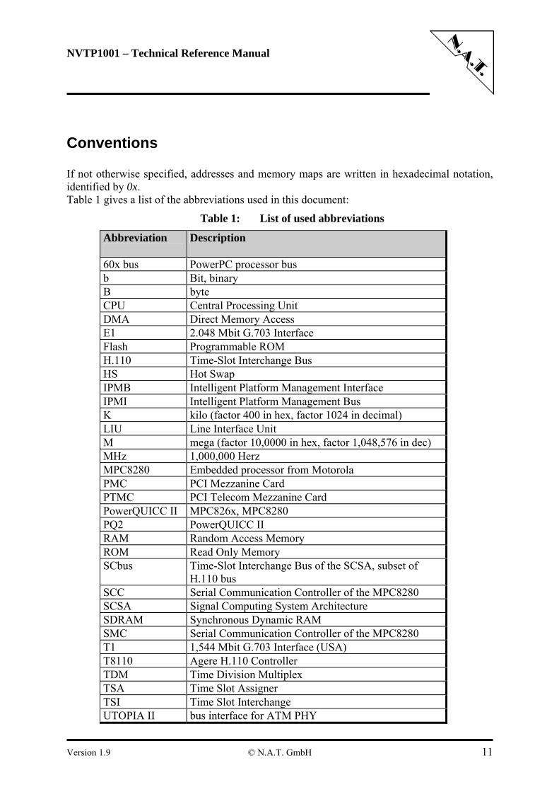
Conventions If not otherwise specified, addresses and memory maps are written in hexadecimal notation, identified by 0x. Table 1 gives a list of the abbreviations used in this document:
Table 1: List of used abbreviations
Abbreviation
Description
60x bus PowerPC processor bus b Bit, binary B byte CPU Central Processing Unit DMA Direct Memory Access E1 2.048 Mbit G.703 Interface Flash Programmable ROM H.110 Time-Slot Interchange Bus HS Hot Swap IPMB Intelligent Platform Management Interface IPMI Intelligent Platform Management Bus K kilo (factor 400 in hex, factor 1024 in decimal) LIU Line Interface Unit M mega (factor 10,0000 in hex, factor 1,048,576 in dec) MHz 1,000,000 Herz MPC8280 Embedded processor from Motorola PMC PCI Mezzanine Card PTMC PCI Telecom Mezzanine Card PowerQUICC II MPC826x, MPC8280 PQ2 PowerQUICC II RAM Random Access Memory ROM Read Only Memory SCbus Time-Slot Interchange Bus of the SCSA, subset of
H.110 bus SCC Serial Communication Controller of the MPC8280 SCSA Signal Computing System Architecture SDRAM Synchronous Dynamic RAM SMC Serial Communication Controller of the MPC8280 T1 1,544 Mbit G.703 Interface (USA) T8110 Agere H.110 Controller TDM Time Division Multiplex TSA Time Slot Assigner TSI Time Slot Interchange UTOPIA II bus interface for ATM PHY
Version 1.9 © N.A.T. GmbH 11
NVTP1001 – Technical Reference Manual
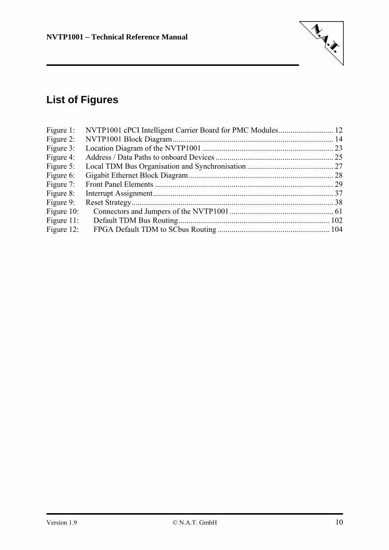
1 Introduction
The NVTP1001 is a high performance PCI Mezzanine Card carrier board especially suited for Telecom and networking applications.
Figure 1: NVTP1001 cPCI Intelligent Carrier Board for PMC Modules
Backplane Connectors
PMC Module
e.g.NPMC-8260-E1/T1
(Back View)
PMC Module
e.g.NPMC-STM1(Back View) MPC8280
CPU
GigabitEthernet
H.110TSI
centralswitchingresource
PCI -> PCIbridge
Version 1.9 © N.A.T. GmbH 12
NVTP1001 – Technical Reference Manual
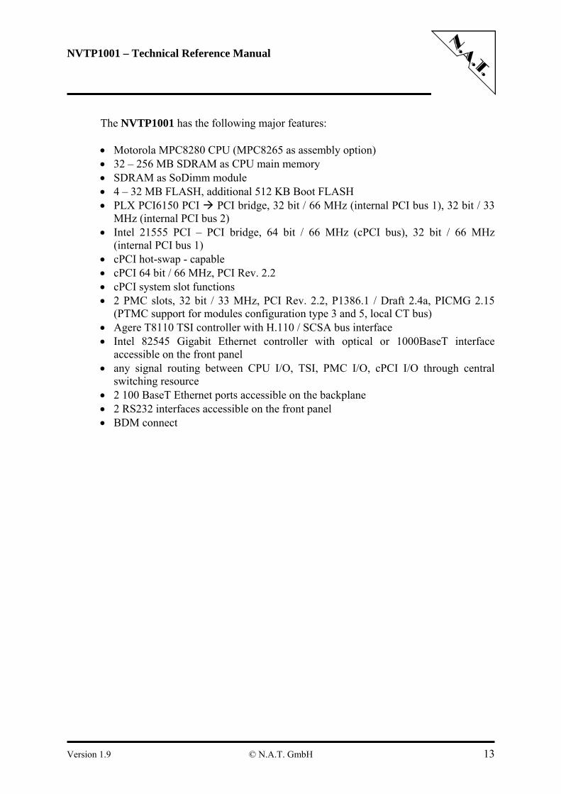
The NVTP1001 has the following major features: • Motorola MPC8280 CPU (MPC8265 as assembly option) • 32 – 256 MB SDRAM as CPU main memory • SDRAM as SoDimm module • 4 – 32 MB FLASH, additional 512 KB Boot FLASH • PLX PCI6150 PCI PCI bridge, 32 bit / 66 MHz (internal PCI bus 1), 32 bit / 33
MHz (internal PCI bus 2) • Intel 21555 PCI – PCI bridge, 64 bit / 66 MHz (cPCI bus), 32 bit / 66 MHz
(internal PCI bus 1) • cPCI hot-swap - capable • cPCI 64 bit / 66 MHz, PCI Rev. 2.2 • cPCI system slot functions • 2 PMC slots, 32 bit / 33 MHz, PCI Rev. 2.2, P1386.1 / Draft 2.4a, PICMG 2.15
(PTMC support for modules configuration type 3 and 5, local CT bus) • Agere T8110 TSI controller with H.110 / SCSA bus interface • Intel 82545 Gigabit Ethernet controller with optical or 1000BaseT interface
accessible on the front panel • any signal routing between CPU I/O, TSI, PMC I/O, cPCI I/O through central
switching resource • 2 100 BaseT Ethernet ports accessible on the backplane • 2 RS232 interfaces accessible on the front panel • BDM connect
Version 1.9 © N.A.T. GmbH 13
NVTP1001 – Technical Reference Manual
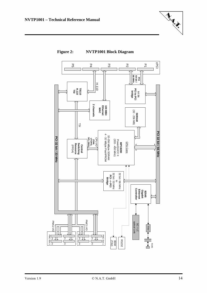
Figure 2: NVTP1001 Block Diagram
cPC
I
PM
C S
lot 2
PM
C S
lot 1
PCI
64 bit / 66 M
Hz
CP
U C
ore:
MPC
8280P
owerQ
UIC
C II
(333 - 450 MH
z)
32-256 MByte SD
RAM
4 - 32 MByte FlashPR
OM
PCI 32 bit / 66 M
Hz
32 bit / 66 MH
zto
32 bit / 33 MH
zPC
I --> PCI
Bridge
64 BitPC
I to PCI
bridge
Central
Switching
Resource(FPG
A)
T8110H
.110TSI
82545G
igabitEthernet
Controller
SC / LC
optical Link
Filter
RS232
BDM
JTAG
PCI 32 bit / 33 M
Hz
P1
P2
P4
P1
P2
P4
P1
P4
P3
P2
P5
H.110
TSI
CP
U I/O
(TDM
,U
TOPIA
,SPI, D
MA
)PM
C1 I/O
PMC
2 I/O
100 MB
itEthernet
MA
C
2 channels
RJ45
P3
P3
SDR
AM
(32 - 256 MB)
Version 1.9 © N.A.T. GmbH 14
NVTP1001 – Technical Reference Manual
1.1 Board Features
• CPU
Depending on the assembled CPU the PowerQUICC II runs with a core clock frequency of 266 - 450 MHz. The user may choose between a MPC8280, or a MPC8265 CPU (assembly option).
Default: MPC8280 CPU installed
• Memory
SDRAM: The NVTP1001 provides 32 to 256 MB SDRAM onboard. The SDRAM is installed as a SODIMM SDRAM module. PC100-type SODIMM modules of 32 MB, 64 MB, 128 MB, and 256 MB are supported. The SDRAM data path is 64 bit wide.
Default: 32 MB installed
Flash PROM: The 16-bit wide Flash PROM provides a maximum capacity of 32 MB
(assembly option).
Default: 16 MB installed Boot Flash: The 8-bit wide Boot Flash provides a capacity of 512 KB (optional).
Default: 512 KB installed
• Interfaces cPCI: The NVTP1001 includes a 32/64 bit 33/66 MHz Compact PCI bus
interface. This is implemented by an Intel i21555 PCI PCI bridge. The cPCI interface supports hot swap. It also implements system slot
functionality (assembly option).
Default: peripheral board, no system slot functionality, hot swap capable int. PCI: The NVTP1001 implements 2 internal PCI busses, a 32 bit / 66 MHz
PCI bus, and a 32 bit / 33 MHz PCI bus. The 32 bit / 66 MHz PCI bus (PCI bus 1) connects the i21555 PCI
PCI bridge to the MPC8280 CPU, to the i82545 Gigabit Ethernet controller, and to the internal, second PCI PCI bridge PLX PCI 6150.
The 32 bit / 33 MHz bus (PCI bus 2) is seperated from PCI bus 1 for
performance reasons. It connects the MPC8280 CPU through the PCI PCI bridge PLX PCI 6150 to the T8110 TSI device, to the 2 PMC slots, and to the 2 AM79C973 Ethernet controllers.
Version 1.9 © N.A.T. GmbH 15
NVTP1001 – Technical Reference Manual
PMC: The NVTP1001 includes a 32 bit / 33 MHz bus interface, which connects to the 2 PMC slots. This is implemented by a PCI PCI bridge PLX PCI 6150.
• I/O
H.110: The NVTP1001 implements a 32 bit H.110 interface according to PICMG 2.5 R1.0. This is implemented by an Agere T8110 TSI device.
TDM, MII, The complete number of I/O pins of the MPC8280 CPU are routed to the UTOPIA 2: central switching resource. Ethernet: The Gigabit Ethernet interface supplied by the i82545 is connected
through a 1000BaseT interface or through an optical link to the front panel (assembly option). Default: 1000BaseT assembled
The two 100 MBit Ethernet interfaces supplied by the 2 AM79C973 (assembly option) are connected through a 100BaseT interface to the cPCI backplane, compliant to PICMG 2.16 R1.0, in order to support fabric systems. Default: assembled
RS232: There are 2 RS232 channels, one of them is available on the front panel,
which is connected to the SMC1 port of the MPC8280 CPM. The other one is available on an onboard header, which is connected to the central switching resource, and thus may be routed to any SCC or SMC2 of the MPC8280 CPM.
P(T)MC: The NVTP1001 2 PMC slots, the I/O pins of which (PMC connector P4)
are completely routed to the Central Switching Resource. In order to support PTMC modules with configuration 3 or 5, the respective pins of PMC connector P3 are also routed to the the Central Switching Resource.
• Central Switching Resource
A major feature of the NVTP1001 is the central switching resource, which adds any possible interconnect flexibility to the routing of I/O and TDM signals. The central switching resource is implemented by a Altera ACEX 1K100 FPGA, which allows routing plus logical transformation of all onboard TDM and I/O signals, plus functionality like routing of SPI, UTOPIA, MII, or DMA handshake signals. The central switching resource is programmed according to the user’s application. The programming may be done after Power-Up by a configuration device EPC2 or during runtime by user software. Details on request.
Default: EPC2 assembled and used as configuration device
Version 1.9 © N.A.T. GmbH 16
NVTP1001 – Technical Reference Manual
1.2 Board Specification
Table 2: NVTP1001 Features
Processor PowerQUICC II MPC8280 (optional MPC8265) based Embedded PowerPC Architecture, 266 to 450 MHz
Board Format standard 6U Compact PCI board
PCI to PMC bus bridge PLX PCI 6150
PCI to cPCI bridge i21555
cPCI functions 64 Bit / 66 MHz PCI, hot swap or system slot (assembly option), with H.110 extension
PMC 2 PMC slots (32 Bit / 33 MHz), support of PTMC interface configuration 3 and 5
Front-I/O RJ45 connector / optical link, Mini-SubD connector, PMC I/O
Main Memory 32 - 256 MByte SDRAM PC100-type
Flash PROM 8 - 32 MByte Flash PROM, onboard programmable
Boot Flash PROM 512 KByte Flash PROM, onboard programmable
Network i82545 Gigabit Ethernet with 10/100/1000BaseT interface or optical link (assembly option) on front panel, 2 AM79C973 with 10/100BaseT interface (assembly option) on backplane
Firmware OK1, VxWorks BSP (on request)
Power consumption
+3.3V 1.5A typ. +5.0V 0.2A typ. + PMC module supply
+5.0V IPMB 0.05A typ., fused with very fast 125mA fuse
note: the +3.3Vpmc supply of the PMC’s is derived from the +5V of the carrier!
Environmental conditions
Temperature (operating): Temperature (storage): Humidity:
0°C to +60°C with forced cooling -40°C to +85°C 10 % to 90 % rh noncondensing
Standards compliance PCI Rev. 2.2 PICMG 2.0 R3.0, PICMG 2.1 R2.0, PICMG 2.3 R1.0, PICMG 2.5 R1.0, PICMG 2.9 R1.0, PICMG 2.12 R2.0, PICMG 2.15 R1.0, PICMG 2.16 R1.0 IEEE P1386.1 / Draft 2.4a
Version 1.9 © N.A.T. GmbH 17

NVTP1001 – Technical Reference Manual
2 Installation
2.1 Safety Note
To ensure proper functioning of the NVTP1001 during its usual lifetime take the following precautions before handling the board.
CAUTION
Electrostatic discharge and incorrect board installation and uninstallation can damage circuits or shorten their lifetime.
• Before installing or uninstalling the NVTP1001 read this installation section • Before installing or uninstalling the NVTP1001 in a rack:
- Check all installed boards and modules for steps that you have to take before turning on or off the power.
- Take those steps. - Finally turn on or off the power.
• Before touching integrated circuits ensure to take all require precautions for handling electrostatic devices.
• Ensure that the NVTP1001 is connected to the backplane via all cPCI connectors and that the power is available on all cPCI connectors (GND, +5V, +3.3V, +12V, -12V).
• When operating the board in areas of strong electromagnetic radiation ensure that the module - is firmly screwed to the rack - and shielded by closed housing
Version 1.9 © N.A.T. GmbH 18
NVTP1001 – Technical Reference Manual
2.2 Installation Prerequisites and Requirements
IMPORTANT
Before powering up • check this section for installation prerequisites and requirements
2.2.1 Requirements
The installation requires only • a carrier board for connecting the NVTP1001 • power supply
2.2.2 Power supply
The power supply for the NVTP1001 must meet the following specifications:
• required for the board: - +3.3V / 1.5A typical - +5V / 0.2A typical
• required for optionally mounted PMC modules: - +5V / 6.0A max. - +12V / 1.0A max. - –12V / 1.0A max.
Refer to User’s Manuals of the PMC modules for information on their power consumption. The numbers given above are the maximum values, if both PMC slots are populated, and each module draws the maximum current allowed from one supply. The overall maximum power allowed to be drawn by both modules together is 15W according to the PMC spec. The power supply of the NVTP1001 supports PPMC modules with up to 30W in total for both slots. In order to prevent excessive loading of the +3.3V supply of the NVTP1001, the +3.3Vpmc supply for the PMC modules is derived from the +5V supply of the NVTP1001 by onboard switching regulators.
Version 1.9 © N.A.T. GmbH 19
NVTP1001 – Technical Reference Manual
2.2.3 Automatic Power Up
In the following situations the NVTP1001 will automatically be reset and proceed with a normal power up:
- The voltage sensor generates a reset
• when any of the cPCI voltages supervised fall out of ±5% tolerance
supervised voltages are: +5V, +3.3V • when any of the internally generated voltages supervised fall out of ±5%
tolerance; supervised voltages are: +2.5V, Vddcore, +2.5Vgig, +1.5V, +3.3Vpmc (+2.5V is the FPGA core voltage, Vddcore is the CPU core voltage, +2.5Vgig and +1,5V are the Gigabit Ethernet controller core- and analogue voltages)
• when the system slot board signals a PCI Reset
- The watchdog times out (if enabled).
Version 1.9 © N.A.T. GmbH 20
NVTP1001 – Technical Reference Manual
2.3 Statement on Environmental Protection
2.3.1 Compliance to RoHS Directive
Directive 2002/95/EC of the European Comission on the "Restriction of the use of certain Hazardous Substances in Electrical and Electronic Equipment" (RoHS) predicts that all electrical and electronic equipment being put on the European market after June 30th, 2006 must contain lead, mercury, hexavalent chromium, polybrominated biphenyls (PBB) and polybrominated diphenyl ethers (PBDE) and cadmium in maximum concentration values of 0.1% respective 0.01% by weight in homogenous materials only.
As these harzadous substances are currently used with semiconductors, plastics (i.e. semiconductor packages, connectors) and soldering tin any hardware product is affected by the RoHS directive if it does not belong to one of the groups of products exempted from the RoHS directive.
Although many of hardware products of N.A.T. are exempted from the RoHS directive it is a declared policy of N.A.T. to provide all products fully compliant to the RoHS directive as soon as possible. For this purpose since January 31st, 2005 N.A.T. is requesting RoHS compliant deliveries from its suppliers. Special attention and care has been payed to the production cycle, so that whereever and whenever possible RoHS components are used with N.A.T. hardware products already.
2.3.2 Compliance to WEEE Directive
Directive 2002/95/EC of the European Comission on "Waste Electrical and Electronic Equipment" (WEEE) predicts that every manufacturer of electrical and electronical equipment which is put on the European market has to contribute to the reuse, recycling and other forms of recovery of such waste so as to reduce disposal. Moreover this directive refers to the Directive 2002/95/EC of the European Comission on the "Restriction of the use of certain Hazardous Substances in Electrical and Electronic Equipment" (RoHS).
Having its main focus on private persons and households using such electrical and electronic equipment the directive also affects business-to-business relationships. The directive is quite restrictive on how such waste of private persons and households has to be handled by the supplier/manufacturer, however, it allows a greater flexibility in business-to-business relationships. This pays tribute to the fact with industrial use electrical and electronical products are commonly intergrated into larger and more complex envionments or systems that cannot easily be split up again when it comes to their disposal at the end of their life cycles.
Version 1.9 © N.A.T. GmbH 21
NVTP1001 – Technical Reference Manual
As N.A.T. products are solely sold to industrial customers, by special arrangement at time of purchase the customer agreed to take the responsibility for a WEEE compliant disposal of the used N.A.T. product. Moreover, all N.A.T. products are marked according to the directive with a crossed out bin to indicate that these products within the European Community must not be disposed with regular waste.
If you have any questions on the policy of N.A.T. regarding the Directive 2002/95/EC of the European Comission on the "Restriction of the use of certain Hazardous Substances in Electrical and Electronic Equipment" (RoHS) or the Directive 2002/95/EC of the European Comission on "Waste Electrical and Electronic Equipment" (WEEE) please contact N.A.T. by phone or e-mail.
2.3.3 Compliance to CE Directive
Compliance to the CE directive is declared. A ‘CE’ sign can ce found on the PCB.
2.3.4 Product Safety
The board complies to EN60950 and UL1950.
Version 1.9 © N.A.T. GmbH 22
NVTP1001 – Technical Reference Manual
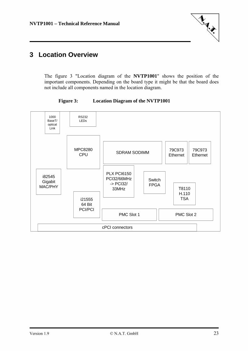
3 Location Overview
The figure 3 "Location diagram of the NVTP1001" shows the position of the important components. Depending on the board type it might be that the board does not include all components named in the location diagram.
Figure 3: Location Diagram of the NVTP1001
1000BaseT/opticalLink
i82545Gigabit
MAC/PHY
MPC8280CPU
RS232LEDs
i2155564 Bit
PCI/PCI
PLX PCI6150PCI32/66MHz
-> PCI32/33MHz
PMC Slot 1 PMC Slot 2
SDRAM SODIMM
T8110H.110TSA
79C973Ethernet
cPCI connectors
SwitchFPGA
79C973Ethernet
Version 1.9 © N.A.T. GmbH 23
NVTP1001 – Technical Reference Manual
4 Functional Blocks
The NVTP1001 can be divided into a number of functional blocks, which are described in the following paragraphs.
4.1 Processor
The MPC8280 PowerQUICC II™ is a versatile communications processor that integrates on one chip a high-performance PowerPC™ RISC microprocessor, a very flexible system integration unit, and many communications peripheral controllers that can be used in a variety of applications, particularly in communications and networking systems.
The core is an embedded variant of the PowerPC MPC603e™ microprocessor family with 16 KB of instruction cache and 16 KB of data cache and no floating-point unit (FPU). The system interface unit (SIU) consists of a flexible memory controller that interfaces to almost any user-defined memory system, and many other peripherals making this device a complete system on a chip.
The communications processor module (CPM) includes four serial communications controllers (SCCs) , with the addition of three high-performance communication channels that support new emerging protocols (for example, 155-Mbps ATM and Fast Ethernet). The MPC8280 has dedicated hardware that can handle up to 256 full-duplex, time-division-multiplexed logical channels (TDM), as well as DMA functionality executing memory to memory and memory to I/O transfers. The optionally available NVTP1001 version with MPC8265 CPU offers the same functionality as the standard version, only the processor and CPM frequencies are reduced.
Version 1.9 © N.A.T. GmbH 24
NVTP1001 – Technical Reference Manual
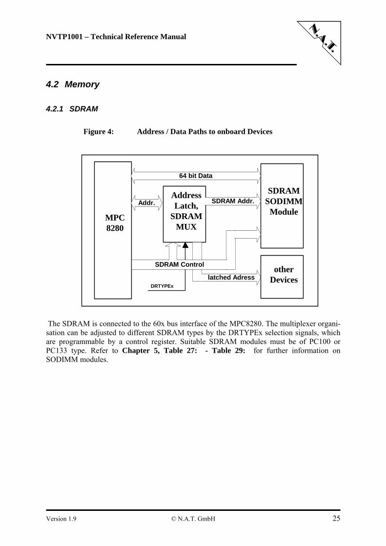
4.2 Memory
4.2.1 SDRAM
Figure 4: Address / Data Paths to onboard Devices
MPC8280
SDRAMSODIMM
Module
64 bit Data
AddressLatch,
SDRAMMUX
SDRAM Addr.Addr.
latched Adressother
Devices
SDRAM Control
DRTYPEx
The SDRAM is connected to the 60x bus interface of the MPC8280. The multiplexer organi-sation can be adjusted to different SDRAM types by the DRTYPEx selection signals, which are programmable by a control register. Suitable SDRAM modules must be of PC100 or PC133 type. Refer to Chapter 5, Table 27: - Table 29: for further information on SODIMM modules.
Version 1.9 © N.A.T. GmbH 25
NVTP1001 – Technical Reference Manual
4.2.2 FLASH There are 2 FLASH devices onboard the NVTP1001, one main FLASH intended for storage of the application software, and one fallback FLASH, which may hold a basic initialisation and monitor program or little kernel, to aid debugging and programming of the main FLASH. Both FLASH devices can be made boot devices by means of the setting of jumper JP7. Please refer to section 6.8 for details on jumper JP7.
4.2.2.1 Main FLASH memory The main FLASH memory is connected to the upper 16 data bits D0 – 15 and to the latched address lines. The FLASH on the NVTP1001 can be programmed either by the CPU (by appropriate software or through the BDM port) or by a PCI bus master. In the latter case the PowerQUICC II has to be prevented from booting from FLASH while this does not contain a defined boot program, in order not to enter unknown states. This can be achieved by installing a jumper (JP6), which disables the MPC8280 CPU core after the following Power-Up cycle. This feature is used for programming the FLASH memory via the PCI bus. Once the FLASH has been programmed, it may be reprogrammed without having to install JP6. Programming software is available on request. Please refer to section 6.7 for details on jumper JP6.
4.2.2.2 Fallback FLASH memory The fallback FLASH memory is connected to the upper 8 data bits D0 – 7 and to the latched address lines. The FLASH on the NVTP1001 can be programmed either by the CPU (by appropriate software or through the BDM port) or by a PCI bus master. Concerning boot device selection and FLASH programming, the description in the previous chapter applies here also. Please refer also to section 6.8.
4.2.3 EEPROM
4.2.3.1 I2C Devices There are two I2C devices on the NVTP1001, which are connected to a control/status register; an EEPROM used for storage of board-specific information, and the EEPROM on the SODIMM SDRAM module, which contains vital data about the SDRAM module size and address organisation. This information is necessary, in order to be able to program the SDRAM controller functions appropriately. The SODIMM I2C device defaults to a 24C02 type, the EEPROM used for storage of board-specific information defaults to 24C08 device. The address of the EEPROM on the SDRAM SODIMM module is 0x0, the address of the other EEPROM is 0x4. Another I2C device (24C02) connects to the PLX PCI 6150. The PCI bridge reads its basic register setup information from this EEPROM on Reset.
4.2.3.2 Microwire Devices There are 5 Microwire devices on the NVTP1001, which are connected to the i21555 PCI PCI bridge (93LC66A), the AM79C973 Ethernet Controller (93LC46A), the T8110 H.110 Controller (93LC46A), and to the i82545 Gigabit Ethernet Controller (93LC46B). The PCI devices read their basic register setup information from these EEPROMs on Reset.
Version 1.9 © N.A.T. GmbH 26
NVTP1001 – Technical Reference Manual
4.3 TDM bus and H.110 Bus Controller
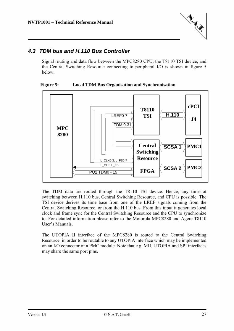
Signal routing and data flow between the MPC8280 CPU, the T8110 TSI device, and the Central Switching Resource connecting to peripheral I/O is shown in figure 5 below.
Figure 5: Local TDM Bus Organisation and Synchronisation
MPC8280
T8110TSI
PQ2 TDM0 - 15
CentralSwitchingResource
FPGA
LREF0-7
cPCI
J4H.110
TDM 0-31
L_CLK, L_FSL_CLK0-3, L_FS0-7
PMC1
PMC2
SCSA 1
SCSA 2
The TDM data are routed through the T8110 TSI device. Hence, any timeslot switching between H.110 bus, Central Switching Resource, and CPU is possible. The TSI device derives its time base from one of the LREF signals coming from the Central Switching Resource, or from the H.110 bus. From this input it generates local clock and frame sync for the Central Switching Resource and the CPU to synchronize to. For detailed information please refer to the Motorola MPC8280 and Agere T8110 User’s Manuals.
The UTOPIA II interface of the MPC8280 is routed to the Central Switching Resource, in order to be routable to any UTOPIA interface which may be implemented on an I/O connector of a PMC module. Note that e.g. MII, UTOPIA and SPI interfaces may share the same port pins.
Version 1.9 © N.A.T. GmbH 27
NVTP1001 – Technical Reference Manual
4.4 Ethernet
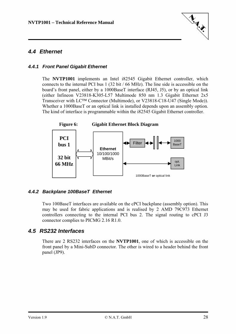
4.4.1 Front Panel Gigabit Ethernet
The NVTP1001 implements an Intel i82545 Gigabit Ethernet controller, which connects to the internal PCI bus 1 (32 bit / 66 MHz). The line side is accessible on the board’s front panel, either by a 1000BaseT interface (RJ45, J5), or by an optical link (either Infineon V23818-K305-L57 Multimode 850 nm 1.3 Gigabit Ethernet 2x5 Transceiver with LC™ Connector (Multimode), or V23818-C18-U47 (Single Mode)). Whether a 1000BaseT or an optical link is installed depends upon an assembly option. The kind of interface is programmable within the i82545 Gigabit Ethernet controller.
Figure 6: Gigabit Ethernet Block Diagram
PCIbus 1
32 bit66 MHz
1000BaseTFilter
Ethernet10/100/1000
MBit/sopt.Link
1000BaseT or optical link
4.4.2 Backplane 100BaseT Ethernet
Two 100BaseT interfaces are available on the cPCI backplane (assembly option). This may be used for fabric applications and is realised by 2 AMD 79C973 Ethernet controllers connecting to the internal PCI bus 2. The signal routing to cPCI J3 connector complies to PICMG 2.16 R1.0.
4.5 RS232 Interfaces
There are 2 RS232 interfaces on the NVTP1001, one of which is accessible on the front panel by a Mini-SubD connector. The other is wired to a header behind the front panel (JP9).
Version 1.9 © N.A.T. GmbH 28
NVTP1001 – Technical Reference Manual
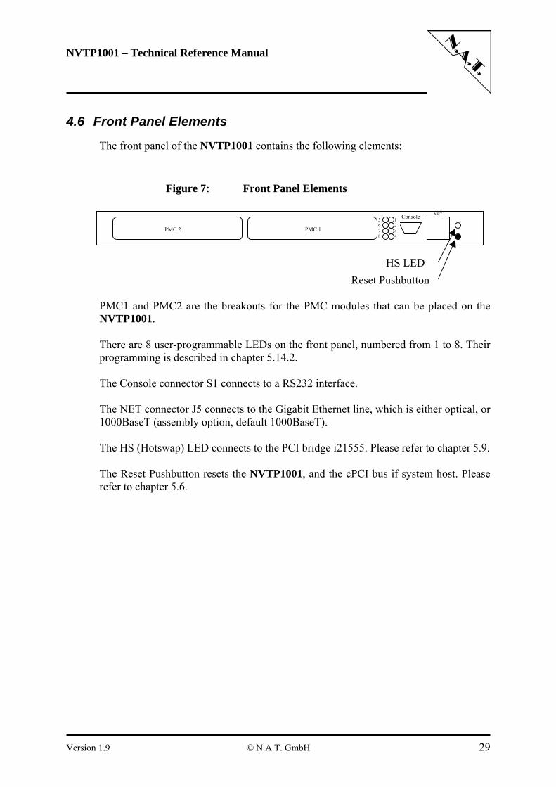
4.6 Front Panel Elements
The front panel of the NVTP1001 contains the following elements:
Figure 7: Front Panel Elements
HS LED
Reset Pushbutton
PMC 2 PMC 1
Console NET1 2 3 4
5678
PMC1 and PMC2 are the breakouts for the PMC modules that can be placed on the NVTP1001. There are 8 user-programmable LEDs on the front panel, numbered from 1 to 8. Their programming is described in chapter 5.14.2. The Console connector S1 connects to a RS232 interface. The NET connector J5 connects to the Gigabit Ethernet line, which is either optical, or 1000BaseT (assembly option, default 1000BaseT). The HS (Hotswap) LED connects to the PCI bridge i21555. Please refer to chapter 5.9. The Reset Pushbutton resets the NVTP1001, and the cPCI bus if system host. Please refer to chapter 5.6.
Version 1.9 © N.A.T. GmbH 29
NVTP1001 – Technical Reference Manual
5 Hardware
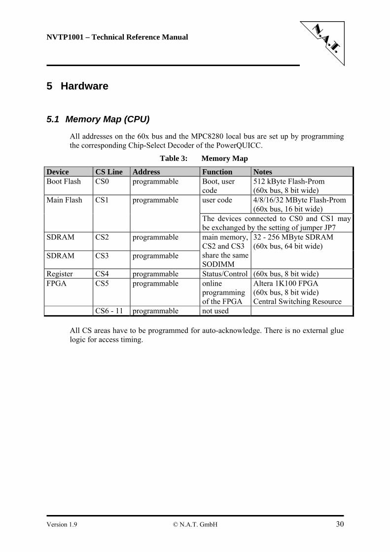
5.1 Memory Map (CPU)
All addresses on the 60x bus and the MPC8280 local bus are set up by programming the corresponding Chip-Select Decoder of the PowerQUICC.
Table 3: Memory Map
Device CS Line Address Function Notes Boot Flash CS0 programmable Boot, user
code 512 kByte Flash-Prom (60x bus, 8 bit wide)
user code 4/8/16/32 MByte Flash-Prom (60x bus, 16 bit wide)
Main Flash CS1 programmable
The devices connected to CS0 and CS1 may be exchanged by the setting of jumper JP7
SDRAM CS2 programmable
SDRAM CS3 programmable
main memory, CS2 and CS3 share the same SODIMM
32 - 256 MByte SDRAM (60x bus, 64 bit wide)
Register CS4 programmable Status/Control (60x bus, 8 bit wide) FPGA CS5 programmable online
programming of the FPGA
Altera 1K100 FPGA (60x bus, 8 bit wide) Central Switching Resource
CS6 - 11 programmable not used
All CS areas have to be programmed for auto-acknowledge. There is no external glue logic for access timing.
Version 1.9 © N.A.T. GmbH 30
NVTP1001 – Technical Reference Manual
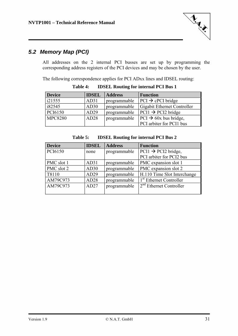
5.2 Memory Map (PCI)
All addresses on the 2 internal PCI busses are set up by programming the corresponding address registers of the PCI devices and may be chosen by the user.
The following correspondence applies for PCI ADxx lines and IDSEL routing:
Table 4: IDSEL Routing for internal PCI Bus 1
Device IDSEL Address Function i21555 AD31 programmable PCI cPCI bridge i82545 AD30 programmable Gigabit Ethernet Controller PCI6150 AD29 programmable PCI1 PCI2 bridge MPC8280 AD28 programmable PCI 60x bus bridge,
PCI arbiter for PCI1 bus
Table 5: IDSEL Routing for internal PCI Bus 2
Device IDSEL Address Function PCI6150 none programmable PCI1 PCI2 bridge,
PCI arbiter for PCI2 bus PMC slot 1 AD31 programmable PMC expansion slot 1 PMC slot 2 AD30 programmable PMC expansion slot 2 T8110 AD29 programmable H.110 Time Slot Interchange AM79C973 AD28 programmable 1st Ethernet Controller AM79C973 AD27 programmable
2nd Ethernet Controller
Version 1.9 © N.A.T. GmbH 31
NVTP1001 – Technical Reference Manual
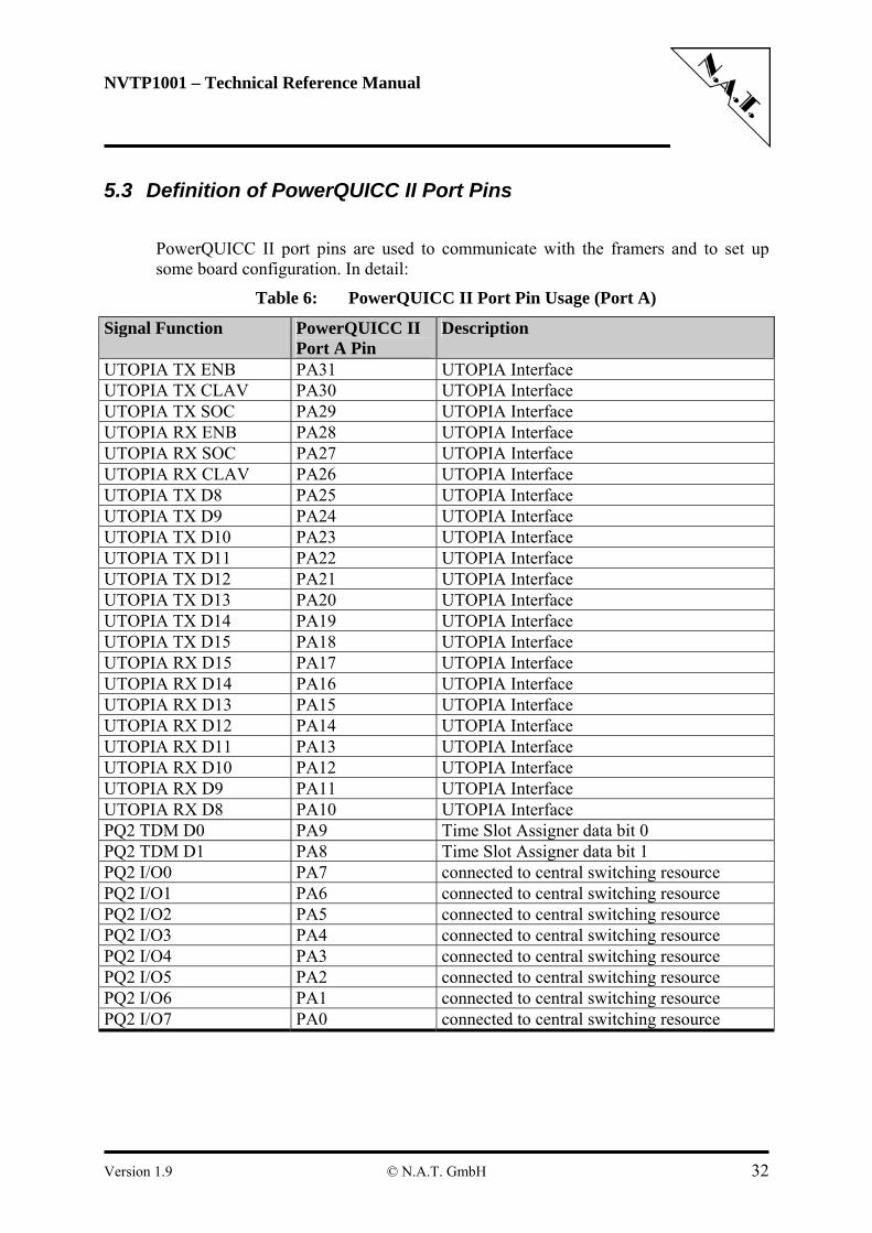
5.3 Definition of PowerQUICC II Port Pins
PowerQUICC II port pins are used to communicate with the framers and to set up some board configuration. In detail:
Table 6: PowerQUICC II Port Pin Usage (Port A)
Signal Function PowerQUICC II Port A Pin
Description
UTOPIA TX ENB PA31 UTOPIA Interface UTOPIA TX CLAV PA30 UTOPIA Interface UTOPIA TX SOC PA29 UTOPIA Interface UTOPIA RX ENB PA28 UTOPIA Interface UTOPIA RX SOC PA27 UTOPIA Interface UTOPIA RX CLAV PA26 UTOPIA Interface UTOPIA TX D8 PA25 UTOPIA Interface UTOPIA TX D9 PA24 UTOPIA Interface UTOPIA TX D10 PA23 UTOPIA Interface UTOPIA TX D11 PA22 UTOPIA Interface UTOPIA TX D12 PA21 UTOPIA Interface UTOPIA TX D13 PA20 UTOPIA Interface UTOPIA TX D14 PA19 UTOPIA Interface UTOPIA TX D15 PA18 UTOPIA Interface UTOPIA RX D15 PA17 UTOPIA Interface UTOPIA RX D14 PA16 UTOPIA Interface UTOPIA RX D13 PA15 UTOPIA Interface UTOPIA RX D12 PA14 UTOPIA Interface UTOPIA RX D11 PA13 UTOPIA Interface UTOPIA RX D10 PA12 UTOPIA Interface UTOPIA RX D9 PA11 UTOPIA Interface UTOPIA RX D8 PA10 UTOPIA Interface PQ2 TDM D0 PA9 Time Slot Assigner data bit 0 PQ2 TDM D1 PA8 Time Slot Assigner data bit 1 PQ2 I/O0 PA7 connected to central switching resource PQ2 I/O1 PA6 connected to central switching resource PQ2 I/O2 PA5 connected to central switching resource PQ2 I/O3 PA4 connected to central switching resource PQ2 I/O4 PA3 connected to central switching resource PQ2 I/O5 PA2 connected to central switching resource PQ2 I/O6 PA1 connected to central switching resource PQ2 I/O7 PA0 connected to central switching resource
Version 1.9 © N.A.T. GmbH 32
NVTP1001 – Technical Reference Manual
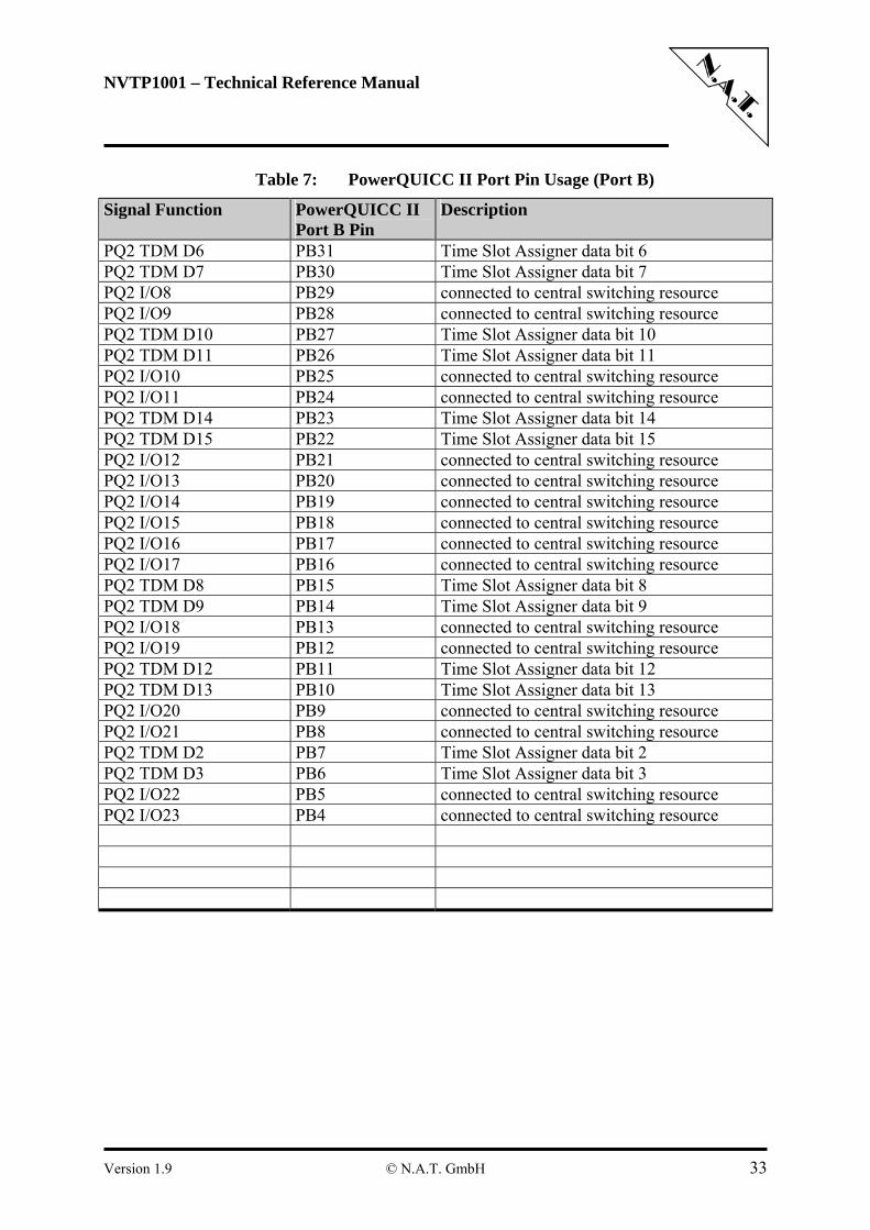
Table 7: PowerQUICC II Port Pin Usage (Port B)
Signal Function PowerQUICC II Port B Pin
Description
PQ2 TDM D6 PB31 Time Slot Assigner data bit 6 PQ2 TDM D7 PB30 Time Slot Assigner data bit 7 PQ2 I/O8 PB29 connected to central switching resource PQ2 I/O9 PB28 connected to central switching resource PQ2 TDM D10 PB27 Time Slot Assigner data bit 10 PQ2 TDM D11 PB26 Time Slot Assigner data bit 11 PQ2 I/O10 PB25 connected to central switching resource PQ2 I/O11 PB24 connected to central switching resource PQ2 TDM D14 PB23 Time Slot Assigner data bit 14 PQ2 TDM D15 PB22 Time Slot Assigner data bit 15 PQ2 I/O12 PB21 connected to central switching resource PQ2 I/O13 PB20 connected to central switching resource PQ2 I/O14 PB19 connected to central switching resource PQ2 I/O15 PB18 connected to central switching resource PQ2 I/O16 PB17 connected to central switching resource PQ2 I/O17 PB16 connected to central switching resource PQ2 TDM D8 PB15 Time Slot Assigner data bit 8 PQ2 TDM D9 PB14 Time Slot Assigner data bit 9 PQ2 I/O18 PB13 connected to central switching resource PQ2 I/O19 PB12 connected to central switching resource PQ2 TDM D12 PB11 Time Slot Assigner data bit 12 PQ2 TDM D13 PB10 Time Slot Assigner data bit 13 PQ2 I/O20 PB9 connected to central switching resource PQ2 I/O21 PB8 connected to central switching resource PQ2 TDM D2 PB7 Time Slot Assigner data bit 2 PQ2 TDM D3 PB6 Time Slot Assigner data bit 3 PQ2 I/O22 PB5 connected to central switching resource PQ2 I/O23 PB4 connected to central switching resource
Version 1.9 © N.A.T. GmbH 33
NVTP1001 – Technical Reference Manual
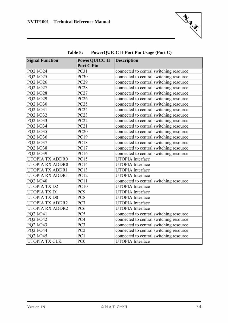
Table 8: PowerQUICC II Port Pin Usage (Port C)
Signal Function PowerQUICC II Port C Pin
Description
PQ2 I/O24 PC31 connected to central switching resource PQ2 I/O25 PC30 connected to central switching resource PQ2 I/O26 PC29 connected to central switching resource PQ2 I/O27 PC28 connected to central switching resource PQ2 I/O28 PC27 connected to central switching resource PQ2 I/O29 PC26 connected to central switching resource PQ2 I/O30 PC25 connected to central switching resource PQ2 I/O31 PC24 connected to central switching resource PQ2 I/O32 PC23 connected to central switching resource PQ2 I/O33 PC22 connected to central switching resource PQ2 I/O34 PC21 connected to central switching resource PQ2 I/O35 PC20 connected to central switching resource PQ2 I/O36 PC19 connected to central switching resource PQ2 I/O37 PC18 connected to central switching resource PQ2 I/O38 PC17 connected to central switching resource PQ2 I/O39 PC16 connected to central switching resource UTOPIA TX ADDR0 PC15 UTOPIA Interface UTOPIA RX ADDR0 PC14 UTOPIA Interface UTOPIA TX ADDR1 PC13 UTOPIA Interface UTOPIA RX ADDR1 PC12 UTOPIA Interface PQ2 I/O40 PC11 connected to central switching resource UTOPIA TX D2 PC10 UTOPIA Interface UTOPIA TX D1 PC9 UTOPIA Interface UTOPIA TX D0 PC8 UTOPIA Interface UTOPIA TX ADDR2 PC7 UTOPIA Interface UTOPIA RX ADDR2 PC6 UTOPIA Interface PQ2 I/O41 PC5 connected to central switching resource PQ2 I/O42 PC4 connected to central switching resource PQ2 I/O43 PC3 connected to central switching resource PQ2 I/O44 PC2 connected to central switching resource PQ2 I/O45 PC1 connected to central switching resource UTOPIA TX CLK PC0 UTOPIA Interface
Version 1.9 © N.A.T. GmbH 34
NVTP1001 – Technical Reference Manual
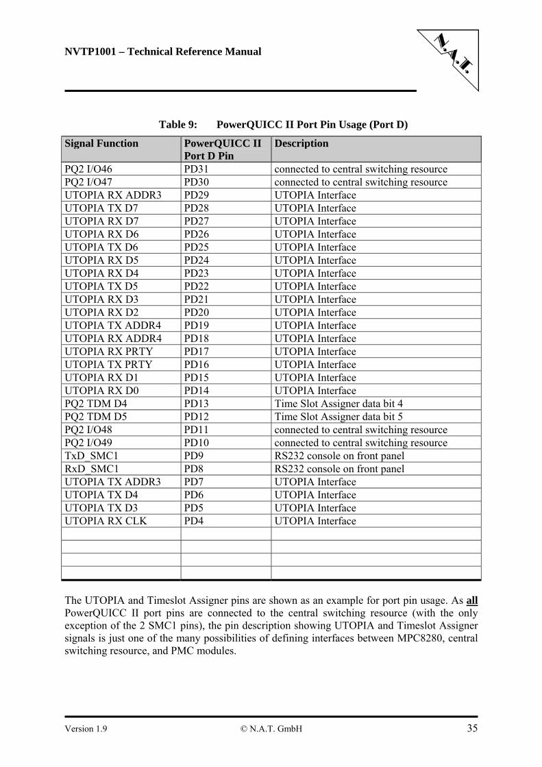
Table 9: PowerQUICC II Port Pin Usage (Port D)
Signal Function PowerQUICC II Port D Pin
Description
PQ2 I/O46 PD31 connected to central switching resource PQ2 I/O47 PD30 connected to central switching resource UTOPIA RX ADDR3 PD29 UTOPIA Interface UTOPIA TX D7 PD28 UTOPIA Interface UTOPIA RX D7 PD27 UTOPIA Interface UTOPIA RX D6 PD26 UTOPIA Interface UTOPIA TX D6 PD25 UTOPIA Interface UTOPIA RX D5 PD24 UTOPIA Interface UTOPIA RX D4 PD23 UTOPIA Interface UTOPIA TX D5 PD22 UTOPIA Interface UTOPIA RX D3 PD21 UTOPIA Interface UTOPIA RX D2 PD20 UTOPIA Interface UTOPIA TX ADDR4 PD19 UTOPIA Interface UTOPIA RX ADDR4 PD18 UTOPIA Interface UTOPIA RX PRTY PD17 UTOPIA Interface UTOPIA TX PRTY PD16 UTOPIA Interface UTOPIA RX D1 PD15 UTOPIA Interface UTOPIA RX D0 PD14 UTOPIA Interface PQ2 TDM D4 PD13 Time Slot Assigner data bit 4 PQ2 TDM D5 PD12 Time Slot Assigner data bit 5 PQ2 I/O48 PD11 connected to central switching resource PQ2 I/O49 PD10 connected to central switching resource TxD_SMC1 PD9 RS232 console on front panel RxD_SMC1 PD8 RS232 console on front panel UTOPIA TX ADDR3 PD7 UTOPIA Interface UTOPIA TX D4 PD6 UTOPIA Interface UTOPIA TX D3 PD5 UTOPIA Interface UTOPIA RX CLK PD4 UTOPIA Interface The UTOPIA and Timeslot Assigner pins are shown as an example for port pin usage. As all PowerQUICC II port pins are connected to the central switching resource (with the only exception of the 2 SMC1 pins), the pin description showing UTOPIA and Timeslot Assigner signals is just one of the many possibilities of defining interfaces between MPC8280, central switching resource, and PMC modules.
Version 1.9 © N.A.T. GmbH 35
NVTP1001 – Technical Reference Manual
5.4 CPU - PLL-Setup
The basic setting of the clocks is done by pulling the MODCK pins during /CPURST. /CPURST is the Reset input of the CPU and valid with Power-On RESET and /PCIRST. These are programmable through CPLD U25 (BA0-2). There are 5 additional pins (PCIMODCKx) responsible for setting the PLLs, which are also read during /PORESET. E.g. the default PLL setting for a MPC8265 CPU is MODCK1 - 3 = 100b and PMODCKH0 - 3 = 0111b for a 300/200 MHz CPU/CPM version, the default PLL setting for a MPC8280 CPU is MODCK1 - 3 = 001b and PMODCKH0 - 3 = 0010b for a 400/266 MHz CPU/CPM version. The clock frequency of the internal PCI Bus 1 is set to 66 MHz by default.
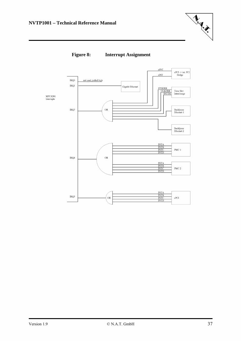
5.5 Interrupt Structure
The NVTP1001 has the following interrupt structure:
Table 10: Interrupt Structure
Interrupt Source
PowerQUICC II Interrupt level
nc IRQ-Level 0 (highest level) Gigabit Ethernet Controller IRQ-Level 1 nc IRQ-Level 2 internal PCI buses (without PMC) IRQ-Level 3 PMC interrupts IRQ-Level 4 external cPCI bus IRQ-Level 5 nc IRQ-Level 6 nc IRQ-Level 7 (lowest level)
The different PCI / PMC interrupts are generated by a logical Wired-Or of the interrupt sources of the respective PCI buses. This is illustrated in Figure 8:. All interrupt sources are readable by status registers. Every interrupt source on the NVTP1001 is maskable by software. The Gigabit Ethernet controller may be masked directly within the MPC8280, as it is the only source to its interrupt pin. All other interrupt sources, which are routed through logic to connect to a CPU interrupt pin, are seperately maskable through Interrupt Mask Registers. The status of these mask registers is also readable. Refer to chapter 5.13 for a detailed description.
Version 1.9 © N.A.T. GmbH 36
NVTP1001 – Technical Reference Manual
Figure 8: Interrupt Assignment
Version 1.9 © N.A.T. GmbH 37
NVTP1001 – Technical Reference Manual
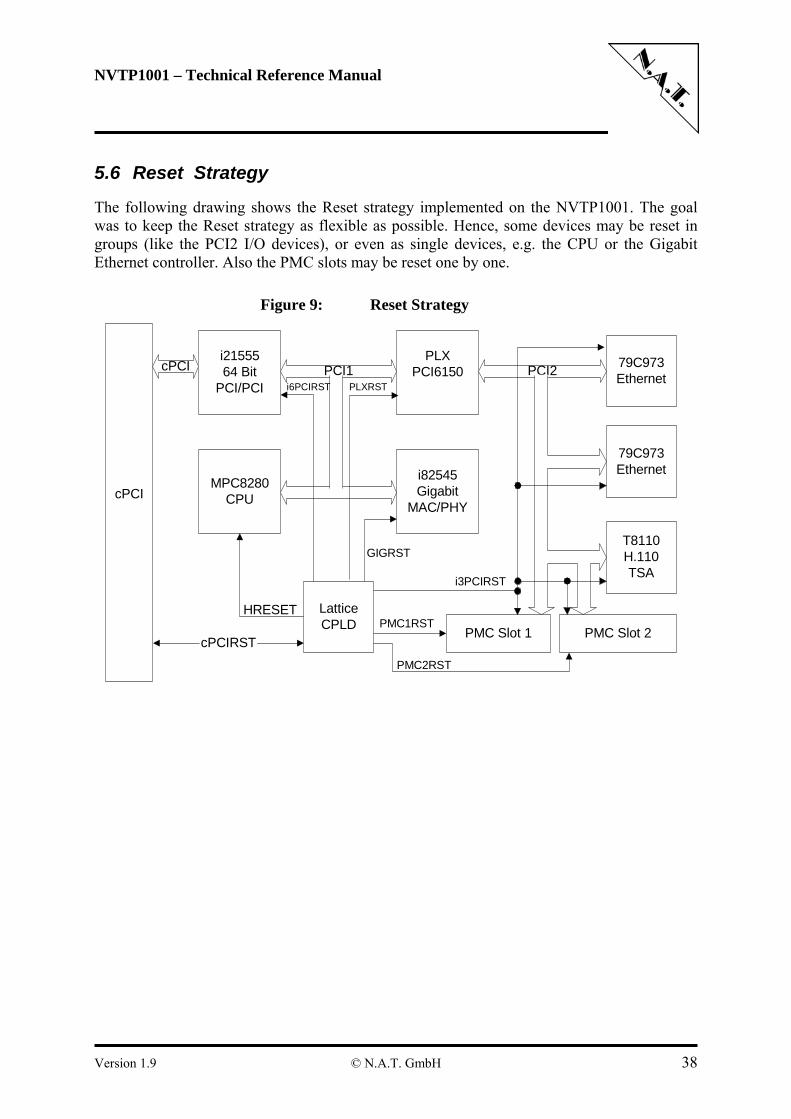
5.6 Reset Strategy
The following drawing shows the Reset strategy implemented on the NVTP1001. The goal was to keep the Reset strategy as flexible as possible. Hence, some devices may be reset in groups (like the PCI2 I/O devices), or even as single devices, e.g. the CPU or the Gigabit Ethernet controller. Also the PMC slots may be reset one by one.
Figure 9: Reset Strategy
PCI1
i82545Gigabit
MAC/PHY
MPC8280CPU
i2155564 Bit
PCI/PCI
PLXPCI6150
PMC Slot 1 PMC Slot 2
T8110H.110TSA
79C973Ethernet
cPCI
LatticeCPLD
79C973Ethernet
cPCI PCI2
cPCIRST
HRESET
i6PCIRST
PMC1RST
GIGRST
i3PCIRST
PMC2RST
PLXRST
Version 1.9 © N.A.T. GmbH 38
NVTP1001 – Technical Reference Manual
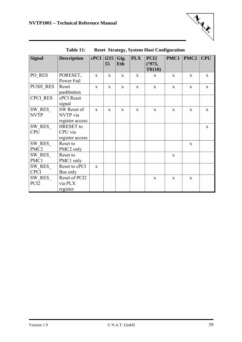
Table 11: Reset Strategy, System Host Configuration
Signal Description cPCI i21555
Gig. Eth
PLX PCI2 (‘973, T8110)
PMC1 PMC2 CPU
PO_RES PORESET, Power Fail
x x x x x x x x
PUSH_RES Reset pushbutton
x x x x x x x x
CPCI_RES cPCI Reset signal
SW_RES_ NVTP
SW Reset of NVTP via register access
x x x x x x x x
SW_RES_ CPU
HRESET to CPU via register access
x
SW_RES_ PMC2
Reset to PMC2 only
x
SW_RES_ PMC1
Reset to PMC1 only
x
SW_RES_ CPCI
Reset to cPCI Bus only
x
SW_RES_ PCI2
Reset of PCI2 via PLX register
x x x
Version 1.9 © N.A.T. GmbH 39

NVTP1001 – Technical Reference Manual
Table 12: Reset Strategy, Peripheral Board Configuration
Signal Description cPCI i21555
Gig. Eth
PLX PCI2
PMC1 PMC2 CPU
PO_RES PORESET, Power Fail
x x x x x x x
PUSH_RES Reset pushbutton
x x x x x x
CPCI_RES cPCI Reset signal
x x x x x x x
SW_RES_ NVTP
SW Reset of NVTP via register access
x x x x x x
SW_RES_ CPU
HRESET to CPU via register access
x
SW_RES_ PMC2
Reset to PMC2 only
x
SW_RES_ PMC1
Reset to PMC1 only
x
SW_RES_ CPCI
Reset to cPCI Bus only
SW_RES_ PCI2
Reset of PCI2 via PLX register
x x x
Version 1.9 © N.A.T. GmbH 40
NVTP1001 – Technical Reference Manual
5.6.1 CPU Reset Sources There are 3 external Reset sources that influence the NVTP1001:
- Power-On Reset / failure of one or more of the power supplies - front panel push button Reset - PCIRST signal of the cPCI bus
The first 2 sources are handled alike by onboard logic, the 3rd is handled, if the NVTP1001 is cPCI peripheral board (i.e. not in system slot), and is ignored if the NVTP1001 is cPCI system host (in system slot). In the latter case PCIRST is driven by the NVTP1001. There are 5 internal Reset sources that influence the NVTP1001:
- Reset to CPU (only) by register access - Reset to CPU, peripherals, and cPCI (if system host) by register access - Reset to PMC module slot 1 - Reset to PMC module slot 2 - Reset to the PCI2 bus (behind the PLX bridge)
These 2 ways of resetting the MPC8280 CPU by register access have to be programmed in software. The major difference between these ways of software reset to the CPU is, that one reset by register access resets only the CPU, and nothing else. The other reset by register access resets also the peripherals, and the cPCI bus (if the board is system host). It’s functionality I the same as when the front panel pushbutton is pressed. Extra Reset signals that reset only the PMC modules can be programmed via a register. Please refer to chapter 5.13.8 for reset by register access. A Reset signal used to resetting the cPCI Bus can be programmed via a register. Please refer to chapter 5.13.8 for reset by register access. This feature will only be available if thw board is configured as system host on the cPCI Bus. Another Reset signal, that resets the peripheral devices on the PCI2 bus may be programmed by software via a PLX bridge register. Apart from the PMC slots, this signal resets the backplane Ethernet channels and the TSI device. Please refer to chapter 5.13.8 for reset by register access.
Version 1.9 © N.A.T. GmbH 41
NVTP1001 – Technical Reference Manual
5.6.2 CPU Reset Pins
The MPC8280 CPU has 3 Reset pins (HRESET, SRESET, PORESET), of which only PORESET is only input and connected to the output of the onboard reset generator. HRESET and SRESET are bidirectional. SRESET is only connected to the BDM interface. HRESET may be driven by a CPLD, as described above. The CPU reset output /PCIRSTO is not used.
5.6.3 Reset of the PCI Buses
The i21555 PCI Bridge, which interfaces between the internal PCI bus 1 of the NVTP1001 and the Compact PCI bus, has 3 Reset pins, which carry special functionalities. P_RST and S_RST_IN are inputs, S_RST is an output. P_RST and S_RST_IN put the device into a well-defined Reset Mode and are functionally identical (wire-ored within the chip). S_RST_IN is not used on the NVTP1001; P_RST is generated by a CPLD, if a Power Fail or a Power-On Reset occurs, and if an external cPCI PCIRST is received, if the system slot functionality of the NVTP1001 is disabled, i.e. the board is not cPCI system master and therefore may be reset by the cPCI bus PCIRST signal. The same reset logic applies to the PLX PCi 6150 bridge. cPCI PCIRST is output to the cPCI bus, if the system slot functionality of the NVTP1001 is enabled, i.e. the board is cPCI system master and located in slot 1. Although slot 1 functionality is an assembly option, being inserted in slot one is sensed automatically, and output of Reset, arbitration and clock signals are enabled appropriately.
Version 1.9 © N.A.T. GmbH 42
NVTP1001 – Technical Reference Manual
5.7 Arbitration of the internal Buses
5.7.1 PCI bus 1
Arbiter of the internal PCI bus 1 (32 bit, 66 MHz) is the MPC8280 CPU.
5.7.2 PCI bus 2
Arbiter of the internal PCI bus 2 (32 bit, 33 MHz) is the PLX PCI 6150 PCI PCI bridge.
5.7.3 60x bus
The arbiter for the 60x bus is the MPC8280-integrated arbiter.
Version 1.9 © N.A.T. GmbH 43
NVTP1001 – Technical Reference Manual
5.8 Slot 1 Functionality
Whether the Intel i21555 PCI bridge acts as System Host of the Compact PCI bus or not depends on the board configuration (slot 1 functionality, assembly option) and on the slot the board is inserted in.
5.8.1 Compact PCI Bus Arbitration If the NVTP1001 is assembled with the assembly option “System Host”, arbitration signals (/GNTx) are driven on the backplane. If the NVTP1001 is assembled with the assembly option “System Slave”, arbitration signal /GNT0 is an input, and the other arbitration signals are tristated.
5.8.2 Compact PCI Bus Clocks If the NVTP1001 is assembled with the assembly option “System Host”, Compact PCI CLK1 – 7 signals are distributed to the backplane. If the NVTP1001 is assembled with the assembly option “System Slave”, Compact PCI CLK0 is an input, and the other clock signals are not connected.
Version 1.9 © N.A.T. GmbH 44
NVTP1001 – Technical Reference Manual
5.9 Hot Swap Capability
If the NVTP1001 is assembled with the assembly option “System Host”, the hot swap feature is disabled, as hot-swap – capable system masters are not defined so far. Signal termination is activated and pulled to V(I/O). If the NVTP1001 is assembled with the assembly option “System Slave”, the hot swap feature is enabled, and PCI signals are precharged to 1V during board insertion. The hot swap capability of the NVTP1001 according to PICMG 2.1 R2.0 complies to “Full Hot Swap”. For “High Availability” applications contact N.A.T. for support.
5.10 IPMI Interface
The NVTP1001 supports IPMI functionality according to PICMG 2.9 specification. The IPMI interface is executed by a local intelligence, a Philips P98LPC922 microcontroller, which is 8051 software-compatible. This microcontroller implements an I2C interface, which connects to the IPMI serial interface. Internally, the IPMI controller is connected to a local I2C interface, which connects to an 8KB EEPROM device (24C08) and to a LM75 temperature sensor located next to the MPC8280 CPU. The IPMI controller also connects to the Central Switching Resource with 11 port pins, which may be used for passing information between the MPC8280 CPU and the P98LPC922 microcontroller, as well as a programming interface in order to in-circuit-programming of the FLASH memory implemented within the P98LPC922 microcontroller. The communication between the P98LPC922 microcontroller port pins and port pins of the MPC8280 may be programmed by a number of SPI registers defined in the register overview of the SPI interface of the Central Switching Resource in chapter 7.9.3.2. A detailed register description can be found in chapter 7.9.3.6. The IPMI devices onboard the NVTP1001 are supplied by the IPMI power supply available on cPCI J1 connector.
Version 1.9 © N.A.T. GmbH 45
NVTP1001 – Technical Reference Manual
5.11 Device Configuration
5.11.1 Onboard PCI devices All onboard PCI devices are configured through the MPC8280 CPU. Some basic configuration may also be done by EEPROM setup sequence on Reset, depending on the type of device.
5.11.2 MPC8280 CPU The configuration of the MPC8280 CPU depends on the setting of the /RSTCONF signal. If this signal is grounded on HRESET, the MPC8280 reads its configuration from the 60x bus. If /RSTCONF is pulled high, a default configuration is chosen, which may be used e.g. for BDM support. On the NVTP1001 this signal is routed to a jumper (JP5), and thus switchable.
Version 1.9 © N.A.T. GmbH 46
NVTP1001 – Technical Reference Manual
5.12 Minibridges
5.12.1 Minibridge of the i21555 PCI Bridge The Minibridge of the i21555 PCI bridge is not used as such. The connected circuitry serves only for serial load support of EEPROM configuration data and Reset configuration defined by logic pin levels during Reset.
5.12.2 Minibridge of the i82545 Gigabit Ethernet Controller The Minibridge of the i82545 is not used.
5.12.3 Minibridges of the AM79C973 Ethernet Controllers The Minibridges of the AM79C973 Ethernet controllers are not used as such. The connected circuitry serves only for Reset configuration defined by logic pin levels during Reset.
5.12.4 Minibridge of the T8110 H.110 TSI Controller The Minibridge of the T8110 TSI controller is not used.
Version 1.9 © N.A.T. GmbH 47
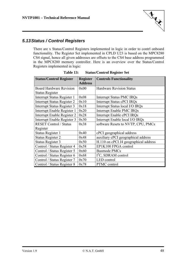
NVTP1001 – Technical Reference Manual
5.13 Status / Control Registers
There are x Status/Control Registers implemented in logic in order to contrl onboard functionality. The Register Set implemented in CPLD U23 is based on the MPC8280 CS4 signal, hence all given addresses are offsets to the CS4 base address programmed in the MPC8280 memory controller. Here is an overview over the Status/Control Registers implemented in logic:
Table 13: Status/Control Register Set
Status/Control Register
Register Address
Controls Functionality
Board Hardware Revision Status Register
0x00 Hardware Revision Status
Interrupt Status Register 1 0x08 Interrupt Status PMC IRQs Interrupt Status Register 2 0x10 Interrupt Status cPCI IRQs Interrupt Status Register 3 0x18 Interrupt Status local I/O IRQs Interrupt Enable Register 1 0x20 Interrupt Enable PMC IRQs Interrupt Enable Register 2 0x28 Interrupt Enable cPCI IRQs Interrupt Enable Register 3 0x30 Interrupt Enable local I/O IRQs RESET Control / Status Register
0x38 software Resets to NVTP, CPU, PMCs
Status Register 1 0x40 cPCI geographical address Status Register 2 0x48 auxiliary cPCI geographical address Status Register 3 0x50 H.110 on cPCI J4 geographical address Control / Status Register 4 0x58 EP1K100 FPGA control Control / Status Register 5 0x60 Busmode PMCs Control / Status Register 6 0x68 I2C, SDRAM control Control / Status Register 7 0x70 LED control Control / Status Register 8 0x78 PTMC control
Version 1.9 © N.A.T. GmbH 48
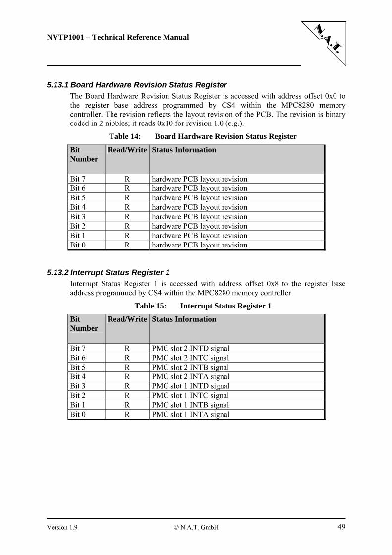
NVTP1001 – Technical Reference Manual
5.13.1 Board Hardware Revision Status Register The Board Hardware Revision Status Register is accessed with address offset 0x0 to the register base address programmed by CS4 within the MPC8280 memory controller. The revision reflects the layout revision of the PCB. The revision is binary coded in 2 nibbles; it reads 0x10 for revision 1.0 (e.g.).
Table 14: Board Hardware Revision Status Register
Bit Number
Read/Write Status Information
Bit 7 R hardware PCB layout revision Bit 6 R hardware PCB layout revision Bit 5 R hardware PCB layout revision Bit 4 R hardware PCB layout revision Bit 3 R hardware PCB layout revision Bit 2 R hardware PCB layout revision Bit 1 R hardware PCB layout revision Bit 0 R hardware PCB layout revision
5.13.2 Interrupt Status Register 1 Interrupt Status Register 1 is accessed with address offset 0x8 to the register base address programmed by CS4 within the MPC8280 memory controller.
Table 15: Interrupt Status Register 1
Bit Number
Read/Write Status Information
Bit 7 R PMC slot 2 INTD signal Bit 6 R PMC slot 2 INTC signal Bit 5 R PMC slot 2 INTB signal Bit 4 R PMC slot 2 INTA signal Bit 3 R PMC slot 1 INTD signal Bit 2 R PMC slot 1 INTC signal Bit 1 R PMC slot 1 INTB signal Bit 0 R PMC slot 1 INTA signal
Version 1.9 © N.A.T. GmbH 49
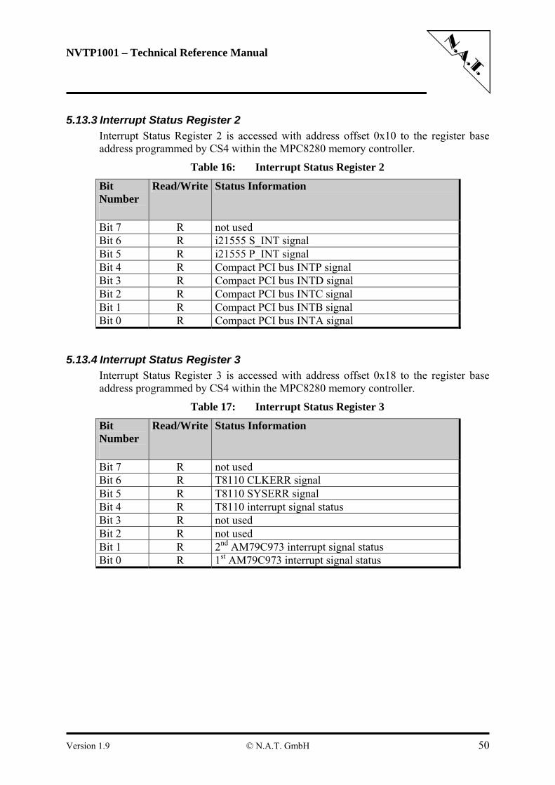
NVTP1001 – Technical Reference Manual
5.13.3 Interrupt Status Register 2 Interrupt Status Register 2 is accessed with address offset 0x10 to the register base address programmed by CS4 within the MPC8280 memory controller.
Table 16: Interrupt Status Register 2
Bit Number
Read/Write Status Information
Bit 7 R not used Bit 6 R i21555 S_INT signal Bit 5 R i21555 P_INT signal Bit 4 R Compact PCI bus INTP signal Bit 3 R Compact PCI bus INTD signal Bit 2 R Compact PCI bus INTC signal Bit 1 R Compact PCI bus INTB signal Bit 0 R Compact PCI bus INTA signal
5.13.4 Interrupt Status Register 3 Interrupt Status Register 3 is accessed with address offset 0x18 to the register base address programmed by CS4 within the MPC8280 memory controller.
Table 17: Interrupt Status Register 3
Bit Number
Read/Write Status Information
Bit 7 R not used Bit 6 R T8110 CLKERR signal Bit 5 R T8110 SYSERR signal Bit 4 R T8110 interrupt signal status Bit 3 R not used Bit 2 R not used Bit 1 R 2nd AM79C973 interrupt signal status Bit 0 R 1st AM79C973 interrupt signal status
Version 1.9 © N.A.T. GmbH 50
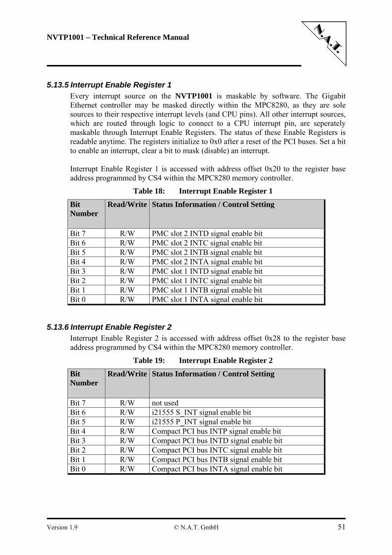
NVTP1001 – Technical Reference Manual
5.13.5 Interrupt Enable Register 1 Every interrupt source on the NVTP1001 is maskable by software. The Gigabit Ethernet controller may be masked directly within the MPC8280, as they are sole sources to their respective interrupt levels (and CPU pins). All other interrupt sources, which are routed through logic to connect to a CPU interrupt pin, are seperately maskable through Interrupt Enable Registers. The status of these Enable Registers is readable anytime. The registers initialize to 0x0 after a reset of the PCI buses. Set a bit to enable an interrupt, clear a bit to mask (disable) an interrupt. Interrupt Enable Register 1 is accessed with address offset 0x20 to the register base address programmed by CS4 within the MPC8280 memory controller.
Table 18: Interrupt Enable Register 1
Bit Number
Read/Write Status Information / Control Setting
Bit 7 R/W PMC slot 2 INTD signal enable bit Bit 6 R/W PMC slot 2 INTC signal enable bit Bit 5 R/W PMC slot 2 INTB signal enable bit Bit 4 R/W PMC slot 2 INTA signal enable bit Bit 3 R/W PMC slot 1 INTD signal enable bit Bit 2 R/W PMC slot 1 INTC signal enable bit Bit 1 R/W PMC slot 1 INTB signal enable bit Bit 0 R/W PMC slot 1 INTA signal enable bit
5.13.6 Interrupt Enable Register 2 Interrupt Enable Register 2 is accessed with address offset 0x28 to the register base address programmed by CS4 within the MPC8280 memory controller.
Table 19: Interrupt Enable Register 2
Bit Number
Read/Write Status Information / Control Setting
Bit 7 R/W not used Bit 6 R/W i21555 S_INT signal enable bit Bit 5 R/W i21555 P_INT signal enable bit Bit 4 R/W Compact PCI bus INTP signal enable bit Bit 3 R/W Compact PCI bus INTD signal enable bit Bit 2 R/W Compact PCI bus INTC signal enable bit Bit 1 R/W Compact PCI bus INTB signal enable bit Bit 0 R/W Compact PCI bus INTA signal enable bit
Version 1.9 © N.A.T. GmbH 51
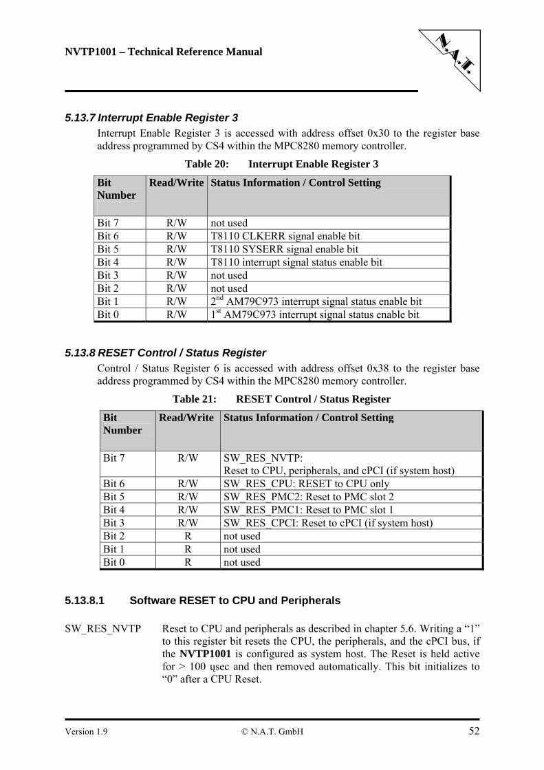
NVTP1001 – Technical Reference Manual
5.13.7 Interrupt Enable Register 3 Interrupt Enable Register 3 is accessed with address offset 0x30 to the register base address programmed by CS4 within the MPC8280 memory controller.
Table 20: Interrupt Enable Register 3
Bit Number
Read/Write Status Information / Control Setting
Bit 7 R/W not used Bit 6 R/W T8110 CLKERR signal enable bit Bit 5 R/W T8110 SYSERR signal enable bit Bit 4 R/W T8110 interrupt signal status enable bit Bit 3 R/W not used Bit 2 R/W not used Bit 1 R/W 2nd AM79C973 interrupt signal status enable bit Bit 0 R/W 1st AM79C973 interrupt signal status enable bit
5.13.8 RESET Control / Status Register Control / Status Register 6 is accessed with address offset 0x38 to the register base address programmed by CS4 within the MPC8280 memory controller.
Table 21: RESET Control / Status Register
Bit Number
Read/Write Status Information / Control Setting
Bit 7 R/W SW_RES_NVTP: Reset to CPU, peripherals, and cPCI (if system host)
Bit 6 R/W SW_RES_CPU: RESET to CPU only Bit 5 R/W SW_RES_PMC2: Reset to PMC slot 2 Bit 4 R/W SW_RES_PMC1: Reset to PMC slot 1 Bit 3 R/W SW_RES_CPCI: Reset to cPCI (if system host) Bit 2 R not used Bit 1 R not used Bit 0 R not used
5.13.8.1 Software RESET to CPU and Peripherals SW_RES_NVTP Reset to CPU and peripherals as described in chapter 5.6. Writing a “1”
to this register bit resets the CPU, the peripherals, and the cPCI bus, if the NVTP1001 is configured as system host. The Reset is held active for > 100 ųsec and then removed automatically. This bit initializes to “0” after a CPU Reset.
Version 1.9 © N.A.T. GmbH 52
NVTP1001 – Technical Reference Manual
5.13.8.2 Software RESET to CPU only SW_RES_CPU Reset to CPU only as described in chapter 5.6. Writing a “1” to this
register bit resets only the CPU. The Reset is held active for > 100 ųsec and then removed automatically. This bit initializes to “0” after a CPU Reset.
5.13.8.3 Software RESET to PMC slots 1 and 2 SW_RES_PMC1, Reset to PMC module located in slot 1 described in chapter 5.6. Writing SW_RES_PMC2 a “1” to this register bit resets the respective PMC module. The Reset is
held active for > 100 ųsec and then removed automatically. The status of the Reset is readable anytime. These bits initialize to “0” after a CPU Reset.
5.13.8.4 Software RESET to cPCI Bus only SW_RES_CPCI Reset to cPCI Bus only as described in chapter 5.6. Writing a “1” to this
register bit resets only the cPCI Bus, if the NVTP1001 is configured as system host. The Reset is held active for > 100 ųsec and then removed automatically. This bit initializes to “0” after a CPU Reset.
Version 1.9 © N.A.T. GmbH 53
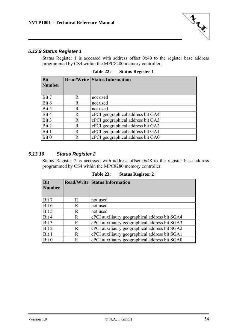
NVTP1001 – Technical Reference Manual
5.13.9 Status Register 1 Status Register 1 is accessed with address offset 0x40 to the register base address programmed by CS4 within the MPC8280 memory controller.
Table 22: Status Register 1
Bit Number
Read/Write Status Information
Bit 7 R not used Bit 6 R not used Bit 5 R not used Bit 4 R cPCI geographical address bit GA4 Bit 3 R cPCI geographical address bit GA3 Bit 2 R cPCI geographical address bit GA2 Bit 1 R cPCI geographical address bit GA1 Bit 0 R cPCI geographical address bit GA0
5.13.10 Status Register 2 Status Register 2 is accessed with address offset 0x48 to the register base address programmed by CS4 within the MPC8280 memory controller.
Table 23: Status Register 2
Bit Number
Read/Write Status Information
Bit 7 R not used Bit 6 R not used Bit 5 R not used Bit 4 R cPCI auxiliaury geographical address bit SGA4 Bit 3 R cPCI auxiliaury geographical address bit SGA3 Bit 2 R cPCI auxiliaury geographical address bit SGA2 Bit 1 R cPCI auxiliaury geographical address bit SGA1 Bit 0 R cPCI auxiliaury geographical address bit SGA0
Version 1.9 © N.A.T. GmbH 54
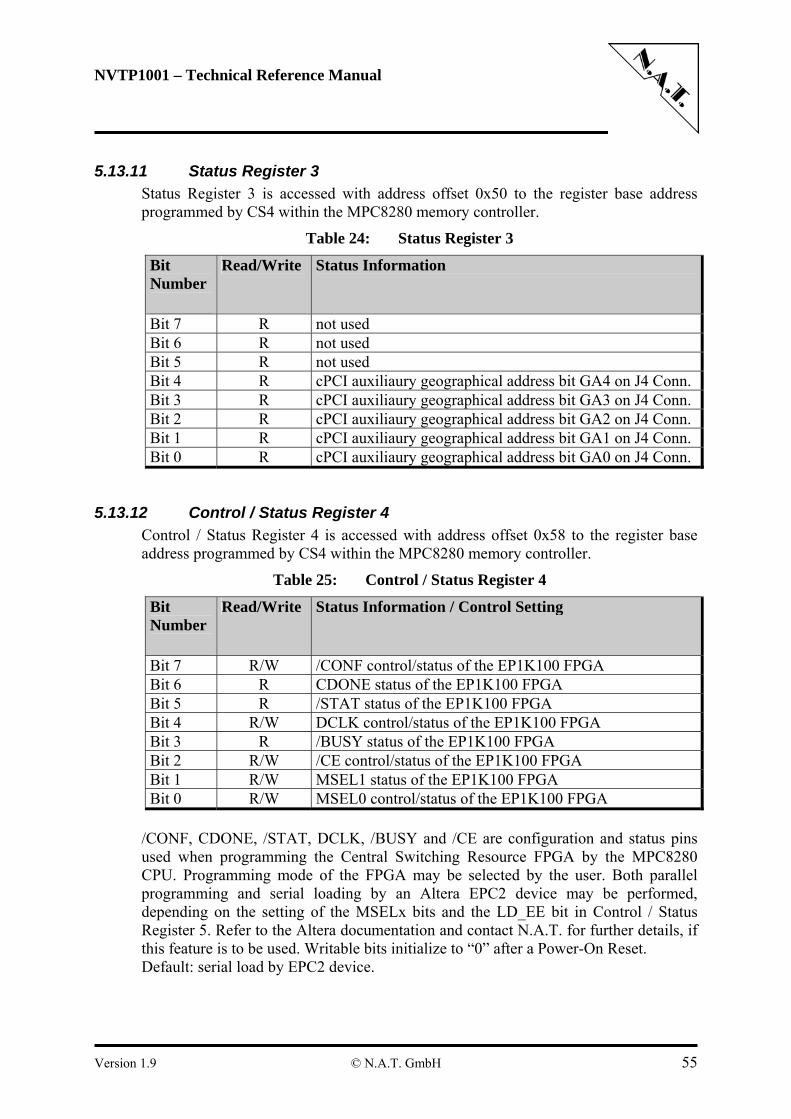
NVTP1001 – Technical Reference Manual
5.13.11 Status Register 3 Status Register 3 is accessed with address offset 0x50 to the register base address programmed by CS4 within the MPC8280 memory controller.
Table 24: Status Register 3
Bit Number
Read/Write Status Information
Bit 7 R not used Bit 6 R not used Bit 5 R not used Bit 4 R cPCI auxiliaury geographical address bit GA4 on J4 Conn. Bit 3 R cPCI auxiliaury geographical address bit GA3 on J4 Conn. Bit 2 R cPCI auxiliaury geographical address bit GA2 on J4 Conn. Bit 1 R cPCI auxiliaury geographical address bit GA1 on J4 Conn. Bit 0 R cPCI auxiliaury geographical address bit GA0 on J4 Conn.
5.13.12 Control / Status Register 4 Control / Status Register 4 is accessed with address offset 0x58 to the register base address programmed by CS4 within the MPC8280 memory controller.
Table 25: Control / Status Register 4
Bit Number
Read/Write Status Information / Control Setting
Bit 7 R/W /CONF control/status of the EP1K100 FPGA Bit 6 R CDONE status of the EP1K100 FPGA Bit 5 R /STAT status of the EP1K100 FPGA Bit 4 R/W DCLK control/status of the EP1K100 FPGA Bit 3 R /BUSY status of the EP1K100 FPGA Bit 2 R/W /CE control/status of the EP1K100 FPGA Bit 1 R/W MSEL1 status of the EP1K100 FPGA Bit 0 R/W MSEL0 control/status of the EP1K100 FPGA
/CONF, CDONE, /STAT, DCLK, /BUSY and /CE are configuration and status pins used when programming the Central Switching Resource FPGA by the MPC8280 CPU. Programming mode of the FPGA may be selected by the user. Both parallel programming and serial loading by an Altera EPC2 device may be performed, depending on the setting of the MSELx bits and the LD_EE bit in Control / Status Register 5. Refer to the Altera documentation and contact N.A.T. for further details, if this feature is to be used. Writable bits initialize to “0” after a Power-On Reset. Default: serial load by EPC2 device.
Version 1.9 © N.A.T. GmbH 55
NVTP1001 – Technical Reference Manual
5.13.13 Control / Status Register 5 Control / Status Register 5 is accessed with address offset 0x60 to the register base address programmed by CS4 within the MPC8280 memory controller.
Table 26: Control / Status Register 5
Bit Number
Read/Write Status Information / Control Setting
Bit 7 R/W LD_EE, defines loading mode of the EP1K100 FPGA Bit 6 R not used Bit 5 R not used Bit 4 R/W BUSMODE 4 signal Bit 3 R/W BUSMODE 3 signal Bit 2 R/W BUSMODE 2 signal Bit 1 R BUSMODE 1 signal of PMC slot 2 Bit 0 R BUSMODE 1 signal of PMC slot 1
By this register the BUSMODE2-4 pins on the PMC modules can be set, and the status of all BUSMODE signals of both slots is readable. BUSMODE2 - 4 are bused and initialize to “1” after a Power-On Reset. Both parallel programming and serial loading by an Altera EPC2 device may be performed, depending on the setting of the MSELx bits in Control / Status Register 4 and the LD_EE bit. Refer to the Altera documentation and contact N.A.T. for further details, if this feature is to be used. LD_EE initializes to “0” after a Power-On Reset. Default: serial load by EPC2 device.
5.13.14 Control / Status Register 6 Control / Status Register 6 is accessed with address offset 0x68 to the register base address programmed by CS4 within the MPC8280 memory controller.
Table 27: Control / Status Register 6
Bit Number
Read/Write Status Information / Control Setting
Bit 7 R not used Bit 6 R not used Bit 5 R not used Bit 4 R not used Bit 3 R/W DRTYPE1 SDRAM Control Signal Bit 2 R/W DRTYPE0 SDRAM Control Signal Bit 1 R/W SCL_PQ I2C Clock Line Bit 0 R/W SDA_PQ I2C Data Line
Version 1.9 © N.A.T. GmbH 56
NVTP1001 – Technical Reference Manual
5.13.14.1 SDRAM Configuration Pins DRTYPE1-0 Two bits of Control / Status Register 6 are used to configure size and array
information of the SDRAM module installed. The correct value for DRTYPE1-0 has to be determined by reading the SDRAM SODIMM EEPROM contents. This EEPROM contains also further information needed to program the SDRAM controller of the MPC8280 appropriately, e.g. row start address and clock cycles needed for SDRAM access. These bits initialize to “0” after a CPU Reset. DRTYPEx settings refer to following SODIMM organisation:
Table 28: Supported SDRAM SODIMM Module Types
DRTYPE1
DRTYPE0
highest column
address to be multiplexed
no. of SDRAM column
addresses
0 0 SDA7 8 0 1 SDA8 9 1 0 SDA9 10 1 1 SDA11 11
SDAx refers to SDRAM SODIMM address pin.
Addresses to be programmed to be output on PowerQUICC II signals BNKSELx:
Table 29: BNKSELx Programming
DRTYPE1
DRTYPE0
BNKSEL2 BNKSEL1
0 0 PB_A19 PB_A20 0 1 PB_A18 PB_A19 1 0 PB_A17 PB_A18 1 1 PB_A16 PB_A17
PB_Ax refers to PowerQUICC II address line Ax. BNKSEL0 is not used. Refer to chapter 7 and to the MPC8280 User’s Manual for a detailed
description on how to program the Memory Controller of the MPC8280.
5.13.14.2 I2C Interface Pins SCL_PQ, I2C interface connected to the SDRAM SODIMM EEPROM and to the SDA_PQ general purpose EEPROM U24. These bits initialize to “1” after a CPU Reset.
Version 1.9 © N.A.T. GmbH 57
NVTP1001 – Technical Reference Manual
5.13.15 Control / Status Register 7 Control / Status Register 7 is accessed with address offset 0x70 to the register base address programmed by CS4 within the MPC8280 memory controller.
Table 30: Control / Status Register 7
Bit Number
Read/Write Status Information / Control Setting
Bit 7 R/W front panel LED 8 Bit 6 R/W front panel LED 7 Bit 5 R/W front panel LED 6 Bit 4 R/W front panel LED 5 Bit 3 R/W front panel LED 4 Bit 2 R/W front panel LED 3 Bit 1 R/W front panel LED 2 Bit 0 R/W front panel LED 1
The front panel LEDs are turned on/off by programming this register. When a bit is set to logic ‘1’, the LED is lit. The register initializes to 0x0 after a CPU Reset, i.e. the LEDs are not lit.
5.13.16 Control / Status Register 8 Control / Status Register 8 is accessed with address offset 0x78 to the register base address programmed by CS4 within the MPC8280 memory controller.
Table 31: Control / Status Register 8
Bit Number
Read/Write Status Information / Control Setting
Bit 7 R/W PMC2_EN Bit 6 R PMC2_ID2 Bit 5 R PMC2_ID1 Bit 4 R PMC2_ID0 Bit 3 R/W PMC1_EN Bit 2 R PMC1_ID2 Bit 1 R PMC1_ID1 Bit 0 R PMC1_ID0
In case of usage of PTMC modules the PTMC ID signals 0 – 2 and the PTMC Enable signals are readable by Control / Status Register 8. The NVTP1001 supports PTMC modules with interface configurations 3 and 5 (TDM bus versions). PTMC Enables are set by programming the respective bits 3 and 7. Writable bits initialize to “0” after a Reset on internal PCI bus 2 or after a software reset to the respective PMCs. Please also refer to chapter 6.11 for more information on PTMC implementation.
Version 1.9 © N.A.T. GmbH 58
NVTP1001 – Technical Reference Manual
5.14 Port Pin Assignment of the Peripheral Devices
5.14.1 Port Pins Assignment of the i82545 Gigabit Ethernet Controller The i82545 Ethernet Controller supplies an 8-bit parallel port, which is wired to the following status / control signals:
Table 32: Port Pins of the i82545 Gigabit Ethernet Controller
Port Pin
Signal Description
SDP7 ACT Link Status of the i82545 SDP6 LINK_UP Link Status of the i82545 SDP5 not used SDP4 not used SDP3 not used SDP2 not used SDP1 LINK1000 Link Status of the i82545 SDP0 LINK100 Link Status of the i82545
Please refer to the i82545 User’s Manual for further information on link stati. The status of the port pin reflects the status of the respective link status pin.
5.14.2 Port Pins of the T8110 H.110 TSI Controller The T8110 H.110 Controller supplies an 8-bit parallel port, which is wired to the following control signals:
Table 33: Port Pins of the T8110 TSI Controller
Port Pin
Signal Description
GP7 CTC8B_SRC H.110 CTC8B Enable GP6 CTC8A_SRC H.110 CTC8A Enable GP5 not used GP4 not used GP3 not used GP2 not used GP1 not used GP0 not used
CTC8A_SRC and CTC8B_SRC are used to switch the series resistors into the CT bus C8 clock and frame if received by the H.110 controller. The clock and frame signals coming from the T8110 H.110 controller and going to the H.110 bus can be enabled or disabled seperately. If a port pin is set high (i.e. set to logic ‘1’), the resistors are connected, if a port pin is set low, the resistors are shorted.
Version 1.9 © N.A.T. GmbH 59
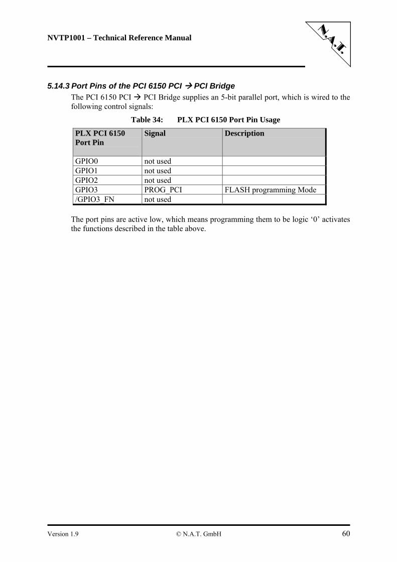
NVTP1001 – Technical Reference Manual
5.14.3 Port Pins of the PCI 6150 PCI PCI Bridge The PCI 6150 PCI PCI Bridge supplies an 5-bit parallel port, which is wired to the following control signals:
Table 34: PLX PCI 6150 Port Pin Usage
PLX PCI 6150 Port Pin
Signal Description
GPIO0 not used GPIO1 not used GPIO2 not used GPIO3 PROG_PCI FLASH programming Mode /GPIO3_FN not used
The port pins are active low, which means programming them to be logic ‘0’ activates the functions described in the table above.
Version 1.9 © N.A.T. GmbH 60
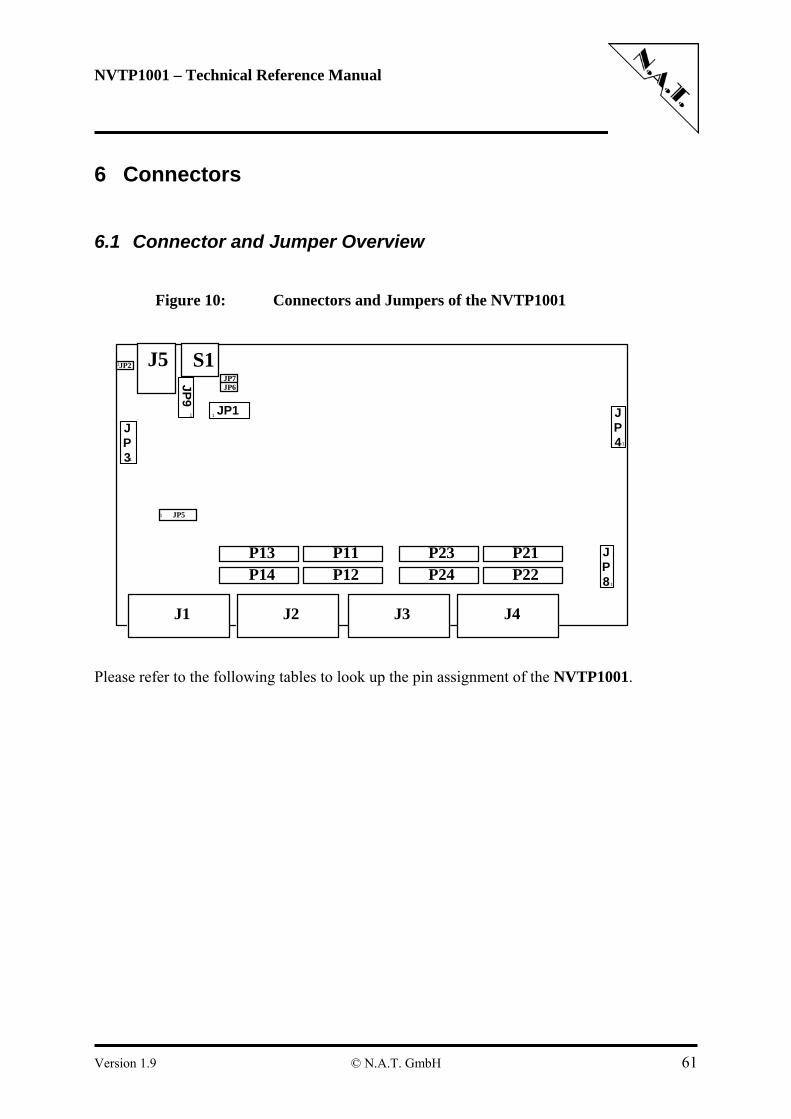
NVTP1001 – Technical Reference Manual
6 Connectors
6.1 Connector and Jumper Overview
Figure 10: Connectors and Jumpers of the NVTP1001
S1J5
P13
JP1
P14P11P12
P23P24
P21P22
JP21
J1 J2 J3 J4
JP8
JP4
JP7
JP5
1
1
JP6JP9
JP31
1 1
1
Please refer to the following tables to look up the pin assignment of the NVTP1001.
Version 1.9 © N.A.T. GmbH 61
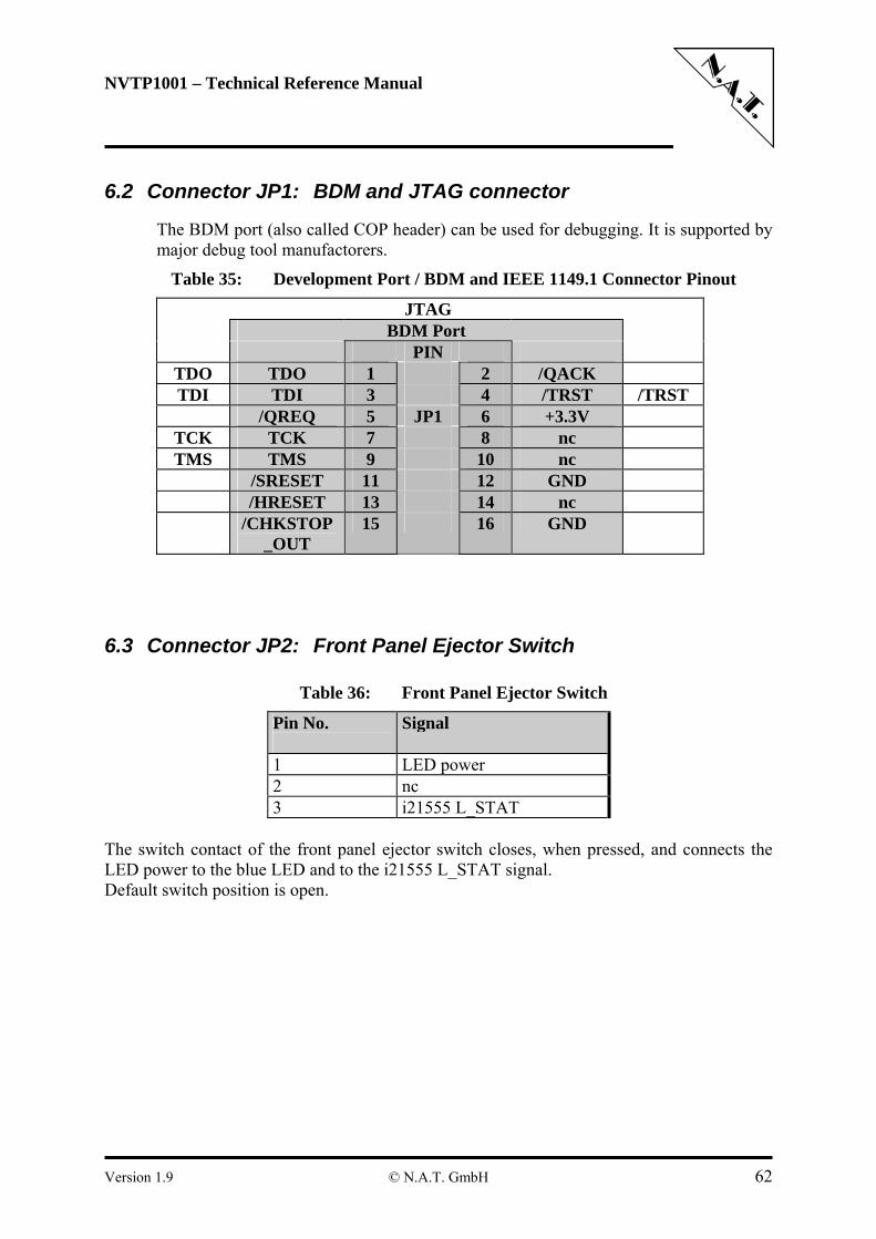
NVTP1001 – Technical Reference Manual
6.2 Connector JP1: BDM and JTAG connector
The BDM port (also called COP header) can be used for debugging. It is supported by major debug tool manufactorers.
Table 35: Development Port / BDM and IEEE 1149.1 Connector Pinout
JTAG BDM Port PIN
TDO TDO 1 2 /QACK TDI TDI 3 4 /TRST /TRST
/QREQ 5 JP1 6 +3.3V TCK TCK 7 8 nc TMS TMS 9 10 nc
/SRESET 11 12 GND /HRESET 13 14 nc /CHKSTOP
_OUT 15 16 GND
6.3 Connector JP2: Front Panel Ejector Switch
Table 36: Front Panel Ejector Switch
Pin No.
Signal
1 LED power 2 nc 3 i21555 L_STAT
The switch contact of the front panel ejector switch closes, when pressed, and connects the LED power to the blue LED and to the i21555 L_STAT signal. Default switch position is open.
Version 1.9 © N.A.T. GmbH 62
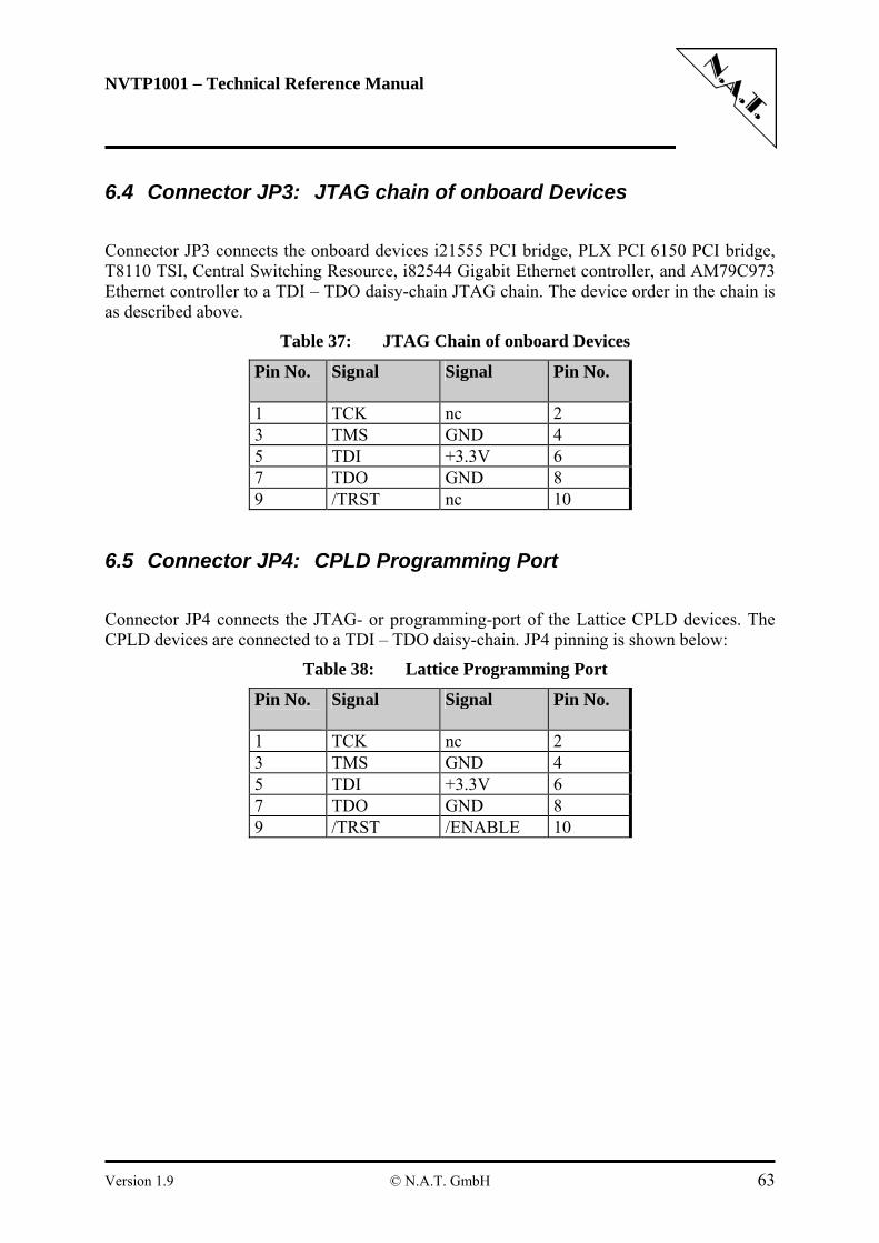
NVTP1001 – Technical Reference Manual
6.4 Connector JP3: JTAG chain of onboard Devices
Connector JP3 connects the onboard devices i21555 PCI bridge, PLX PCI 6150 PCI bridge, T8110 TSI, Central Switching Resource, i82544 Gigabit Ethernet controller, and AM79C973 Ethernet controller to a TDI – TDO daisy-chain JTAG chain. The device order in the chain is as described above.
Table 37: JTAG Chain of onboard Devices
Pin No.
Signal Signal Pin No.
1 TCK nc 2 3 TMS GND 4 5 TDI +3.3V 6 7 TDO GND 8 9 /TRST nc 10
6.5 Connector JP4: CPLD Programming Port
Connector JP4 connects the JTAG- or programming-port of the Lattice CPLD devices. The CPLD devices are connected to a TDI – TDO daisy-chain. JP4 pinning is shown below:
Table 38: Lattice Programming Port
Pin No.
Signal Signal Pin No.
1 TCK nc 2 3 TMS GND 4 5 TDI +3.3V 6 7 TDO GND 8 9 /TRST /ENABLE 10
Version 1.9 © N.A.T. GmbH 63
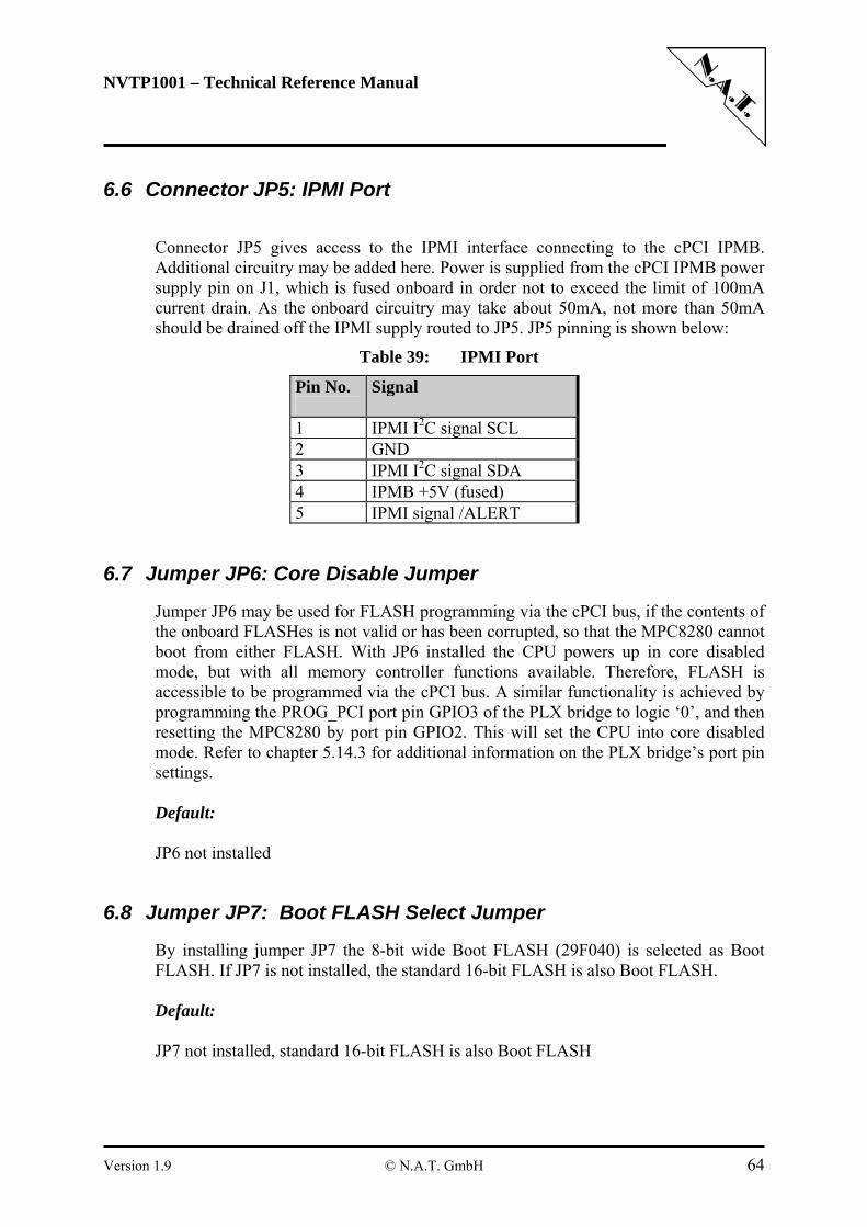
NVTP1001 – Technical Reference Manual
6.6 Connector JP5: IPMI Port
Connector JP5 gives access to the IPMI interface connecting to the cPCI IPMB. Additional circuitry may be added here. Power is supplied from the cPCI IPMB power supply pin on J1, which is fused onboard in order not to exceed the limit of 100mA current drain. As the onboard circuitry may take about 50mA, not more than 50mA should be drained off the IPMI supply routed to JP5. JP5 pinning is shown below:
Table 39: IPMI Port
Pin No.
Signal
1 IPMI I2C signal SCL 2 GND 3 IPMI I2C signal SDA 4 IPMB +5V (fused) 5 IPMI signal /ALERT
6.7 Jumper JP6: Core Disable Jumper
Jumper JP6 may be used for FLASH programming via the cPCI bus, if the contents of the onboard FLASHes is not valid or has been corrupted, so that the MPC8280 cannot boot from either FLASH. With JP6 installed the CPU powers up in core disabled mode, but with all memory controller functions available. Therefore, FLASH is accessible to be programmed via the cPCI bus. A similar functionality is achieved by programming the PROG_PCI port pin GPIO3 of the PLX bridge to logic ‘0’, and then resetting the MPC8280 by port pin GPIO2. This will set the CPU into core disabled mode. Refer to chapter 5.14.3 for additional information on the PLX bridge’s port pin settings. Default: JP6 not installed
6.8 Jumper JP7: Boot FLASH Select Jumper
By installing jumper JP7 the 8-bit wide Boot FLASH (29F040) is selected as Boot FLASH. If JP7 is not installed, the standard 16-bit FLASH is also Boot FLASH. Default: JP7 not installed, standard 16-bit FLASH is also Boot FLASH
Version 1.9 © N.A.T. GmbH 64
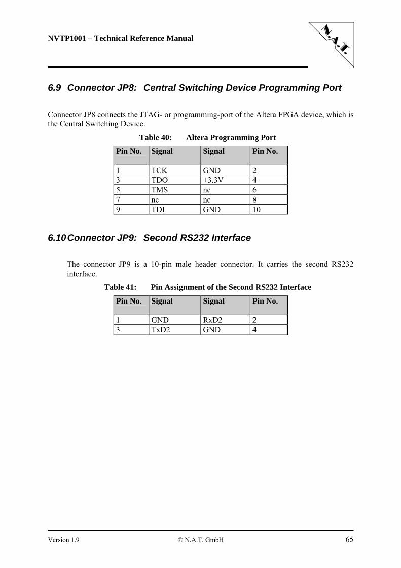
NVTP1001 – Technical Reference Manual
6.9 Connector JP8: Central Switching Device Programming Port
Connector JP8 connects the JTAG- or programming-port of the Altera FPGA device, which is the Central Switching Device.
Table 40: Altera Programming Port
Pin No.
Signal Signal Pin No.
1 TCK GND 2 3 TDO +3.3V 4 5 TMS nc 6 7 nc nc 8 9 TDI GND 10
6.10 Connector JP9: Second RS232 Interface
The connector JP9 is a 10-pin male header connector. It carries the second RS232 interface.
Table 41: Pin Assignment of the Second RS232 Interface
Pin No.
Signal Signal Pin No.
1 GND RxD2 2 3 TxD2 GND 4
Version 1.9 © N.A.T. GmbH 65
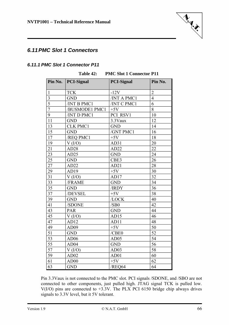
NVTP1001 – Technical Reference Manual
6.11 PMC Slot 1 Connectors
6.11.1 PMC Slot 1 Connector P11
Table 42: PMC Slot 1 Connector P11
Pin No.
PCI-Signal PCI-Signal Pin No.
1 TCK -12V 2 3 GND /INT A PMC1 4 5 /INT B PMC1 /INT C PMC1 6 7 /BUSMODE1 PMC1 +5V 8 9 /INT D PMC1 PCI_RSV1 10 11 GND 3.3Vaux 12 13 CLK PMC1 GND 14 15 GND /GNT PMC1 16 17 /REQ PMC1 +5V 18 19 V (I/O) AD31 20 21 AD28 AD22 22 23 AD25 GND 24 25 GND CBE3 26 27 AD22 AD21 28 29 AD19 +5V 30 31 V (I/O) AD17 32 33 /FRAME GND 34 35 GND /IRDY 36 37 /DEVSEL +5V 38 39 GND /LOCK 40 41 /SDONE /SB0 42 43 PAR GND 44 45 V (I/O) AD15 46 47 AD12 AD11 48 49 AD09 +5V 50 51 GND /CBE0 52 53 AD06 AD05 54 55 AD04 GND 56 57 V (I/O) AD03 58 59 AD02 AD01 60 61 AD00 +5V 62 63 GND /REQ64 64
Pin 3.3Vaux is not connected to the PMC slot. PCI signals /SDONE, and /SBO are not connected to other components, just pulled high. JTAG signal TCK is pulled low. V(I/O) pins are connected to +3.3V. The PLX PCI 6150 bridge chip always drives signals to 3.3V level, but it 5V tolerant.
Version 1.9 © N.A.T. GmbH 66

NVTP1001 – Technical Reference Manual
6.11.2 PMC Slot 1 Connector P12
Table 43: PMC Slot 1 Connector P12
Pin No.
PCI-Signal PCI-Signal Pin No.
1 +12V /TRST 2 3 TMS TDO 4 5 TDI GND 6 7 GND PCI_RSV3 8 9 PCI_RSV PCI_RSV4 10 11 /BUSMODE2 +3.3V 12 13 /PCIRST /BUSMODE3 14 15 +3.3V /BUSMODE4 16 17 /PME PMC1 GND 18 19 AD30 AD29 20 21 GND AD26 22 23 AD24 +3.3V 24 25 IDSEL PMC1 AD23 26 27 +3.3V AD20 28 29 AD18 GND 30 31 AD16 /CBE2 32 33 GND PCI_RESVD 34 35 /TRDY +3.3V 36 37 GND /STOP 38 39 /PERR GND 40 41 +3.3V /SERR 42 43 /CBE1 GND 44 45 AD14 AD13 46 47 M66EN AD10 48 49 AD08 +3.3V 50 51 AD07 PCI_RESV 52 53 +3.3V PCI_RESV 54 55 PCI_RESV GND 56 57 PCI_RESV PCI_RESV 58 59 GND PCI_RESV 60 61 ACK64 +3.3V 62 63 GND PCI_RESV 64
JTAG signals TMS, TDI, and TDO are not connected to the PMC slot. JTAG signal /TRST is pulled low. Signals labelled xxx PMCx are private for this PMC slot, signals without this attachment are bused to both PMC slots.
Version 1.9 © N.A.T. GmbH 67

NVTP1001 – Technical Reference Manual
6.11.3 PMC Slot 1 Connector P13
Table 44: PMC Slot 1 Connector P13
Pin No.
PCI-Signal PCI-Signal Pin No.
1 PMC1_I/O59 GND 2 3 GND PMC1_STX 4 5 PMC1_I/O56 PMC1_SRX 6 7 PMC1_I/O54 GND 8 9 PMC1_PTID2 PMC1_I/O64 10 11 GND PMC1_I/O62 12 13 PMC1_I/O52 GND 14 15 GND PMC1_I/O60 16 17 PMC1_I/O39 PMC1_I/O58 18 19 PMC1_I/O38 GND 20 21 PMC1_PTID0 PMC1_I/O55 22 23 GND PMC1_I/O53 24 25 PMC1_I/O46 GND 26 27 GND PMC1_I/O50 28 29 PMC1_I/O49 PMC1_I/O48 30 31 PMC1_I/O47 GND 32 33 GND PMC1_I/O40 34 35 PMC1_I/O3 PMC1_I/O63 36 37 PMC1_I/O5 GND 38 39 PMC1_PTENB PMC1_I/O61 40 41 GND PMC1_I/O41 42 43 PMC1_I/O45 GND 44 45 GND PMC1_I/O2 46 47 PMC1_I/O8 PMC1_I/O4 48 49 PMC1_I/O10 PMC1_I/O7 50 51 GND PMC1_I/O9 52 53 PMC1_I/O13 PMC1_I/O11 54 55 PMC1_I/O15 GND 56 57 PMC1_PTID1 PMC1_I/O14 58 59 PMC1_I/O17 PMC1_I/O16 60 61 PMC1_I/O20 GND 62 63 GND PMC1_I/O18 64
The I/O signal numbering refers to the signal numbering used in Table 45: below. The reason for double signal routing for these I/O pins is the attempt to support both standard N.A.T. PMC modules with TDM signals on P14 as well as PTMC modules with TDM signals on P13.
Version 1.9 © N.A.T. GmbH 68

NVTP1001 – Technical Reference Manual
6.11.4 PMC Slot 1 Connector P14 ( PMC 1 I/O )
Table 45: PMC Slot 1 Connector P14
ext. Signal
Pin No. PCI-Signal PCI-Signal Pin No. ext. Signal
PMC1_I/O1 1 I/O I/O 2 PMC1_I/O2 PMC1_I/O3 3 I/O I/O 4 PMC1_I/O4 PMC1_I/O5 5 I/O I/O 6 PMC1_I/O6 PMC1_I/O7 7 I/O I/O 8 PMC1_I/O8 PMC1_I/O9 9 I/O I/O 10 PMC1_I/O10 PMC1_I/O11 11 I/O I/O 12 PMC1_I/O12 PMC1_I/O13 13 I/O I/O 14 PMC1_I/O14 PMC1_I/O15 15 I/O I/O 16 PMC1_I/O16 PMC1_I/O17 17 I/O I/O 18 PMC1_I/O18 PMC1_I/O19 19 I/O I/O 20 PMC1_I/O20 PMC1_I/O21 21 I/O I/O 22 PMC1_I/O22 PMC1_I/O23 23 I/O I/O 24 PMC1_I/O24 PMC1_I/O25 25 I/O I/O 26 PMC1_I/O26 PMC1_I/O27 27 I/O I/O 28 PMC1_I/O28 PMC1_I/O29 29 I/O I/O 30 PMC1_I/O30 PMC1_I/O31 31 I/O I/O 32 PMC1_I/O32 PMC1_I/O33 33 I/O I/O 34 PMC1_I/O34 PMC1_I/O35 35 I/O I/O 36 PMC1_I/O36 PMC1_I/O37 37 I/O I/O 38 PMC1_I/O38 PMC1_I/O39 39 I/O I/O 40 PMC1_I/O40 PMC1_I/O41 41 I/O I/O 42 PMC1_I/O42 PMC1_I/O43 43 I/O I/O 44 PMC1_I/O44 PMC1_I/O45 45 I/O I/O 46 PMC1_I/O46 PMC1_I/O47 47 I/O I/O 48 PMC1_I/O48 PMC1_I/O49 49 I/O I/O 50 PMC1_I/O50 PMC1_I/O51 51 I/O I/O 52 PMC1_I/O52 PMC1_I/O53 53 I/O I/O 54 PMC1_I/O54 PMC1_I/O55 55 I/O I/O 56 PMC1_I/O56 PMC1_I/O57 57 I/O I/O 58 PMC1_I/O58 PMC1_I/O59 59 I/O I/O 60 PMC1_I/O60 PMC1_I/O61 61 I/O I/O 62 PMC1_I/O62 PMC1_I/O63 63 I/O I/O 64 PMC1_I/O64
Version 1.9 © N.A.T. GmbH 69
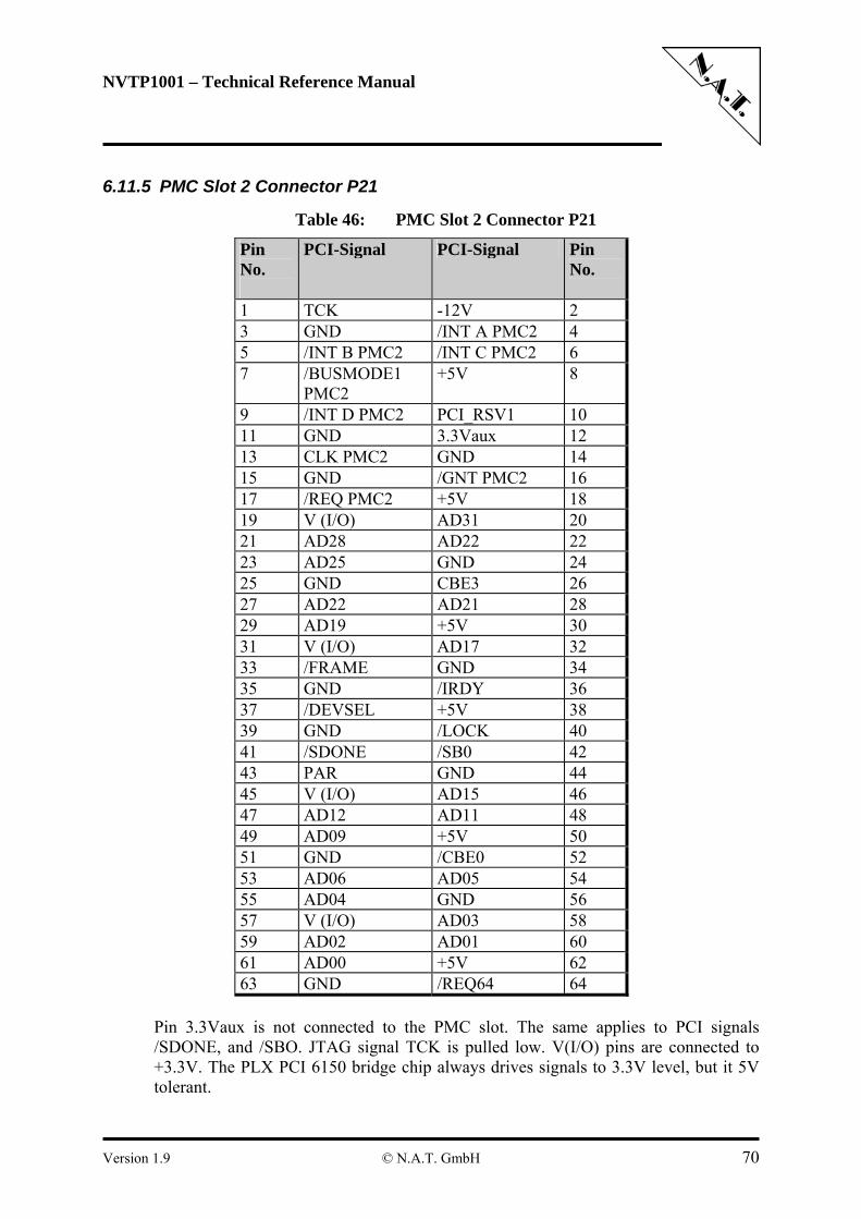
NVTP1001 – Technical Reference Manual
6.11.5 PMC Slot 2 Connector P21
Table 46: PMC Slot 2 Connector P21
Pin No.
PCI-Signal PCI-Signal Pin No.
1 TCK -12V 2 3 GND /INT A PMC2 4 5 /INT B PMC2 /INT C PMC2 6 7 /BUSMODE1
PMC2 +5V 8
9 /INT D PMC2 PCI_RSV1 10 11 GND 3.3Vaux 12 13 CLK PMC2 GND 14 15 GND /GNT PMC2 16 17 /REQ PMC2 +5V 18 19 V (I/O) AD31 20 21 AD28 AD22 22 23 AD25 GND 24 25 GND CBE3 26 27 AD22 AD21 28 29 AD19 +5V 30 31 V (I/O) AD17 32 33 /FRAME GND 34 35 GND /IRDY 36 37 /DEVSEL +5V 38 39 GND /LOCK 40 41 /SDONE /SB0 42 43 PAR GND 44 45 V (I/O) AD15 46 47 AD12 AD11 48 49 AD09 +5V 50 51 GND /CBE0 52 53 AD06 AD05 54 55 AD04 GND 56 57 V (I/O) AD03 58 59 AD02 AD01 60 61 AD00 +5V 62 63 GND /REQ64 64
Pin 3.3Vaux is not connected to the PMC slot. The same applies to PCI signals /SDONE, and /SBO. JTAG signal TCK is pulled low. V(I/O) pins are connected to +3.3V. The PLX PCI 6150 bridge chip always drives signals to 3.3V level, but it 5V tolerant.
Version 1.9 © N.A.T. GmbH 70
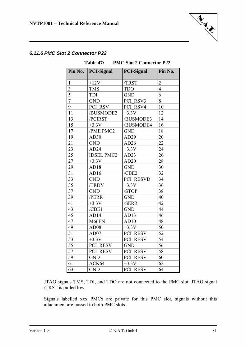
NVTP1001 – Technical Reference Manual
6.11.6 PMC Slot 2 Connector P22
Table 47: PMC Slot 2 Connector P22
Pin No.
PCI-Signal PCI-Signal Pin No.
1 +12V /TRST 2 3 TMS TDO 4 5 TDI GND 6 7 GND PCI_RSV3 8 9 PCI_RSV PCI_RSV4 10 11 /BUSMODE2 +3.3V 12 13 /PCIRST /BUSMODE3 14 15 +3.3V /BUSMODE4 16 17 /PME PMC2 GND 18 19 AD30 AD29 20 21 GND AD26 22 23 AD24 +3.3V 24 25 IDSEL PMC2 AD23 26 27 +3.3V AD20 28 29 AD18 GND 30 31 AD16 /CBE2 32 33 GND PCI_RESVD 34 35 /TRDY +3.3V 36 37 GND /STOP 38 39 /PERR GND 40 41 +3.3V /SERR 42 43 /CBE1 GND 44 45 AD14 AD13 46 47 M66EN AD10 48 49 AD08 +3.3V 50 51 AD07 PCI_RESV 52 53 +3.3V PCI_RESV 54 55 PCI_RESV GND 56 57 PCI_RESV PCI_RESV 58 59 GND PCI_RESV 60 61 ACK64 +3.3V 62 63 GND PCI_RESV 64
JTAG signals TMS, TDI, and TDO are not connected to the PMC slot. JTAG signal /TRST is pulled low. Signals labelled xxx PMCx are private for this PMC slot, signals without this attachment are bussed to both PMC slots.
Version 1.9 © N.A.T. GmbH 71
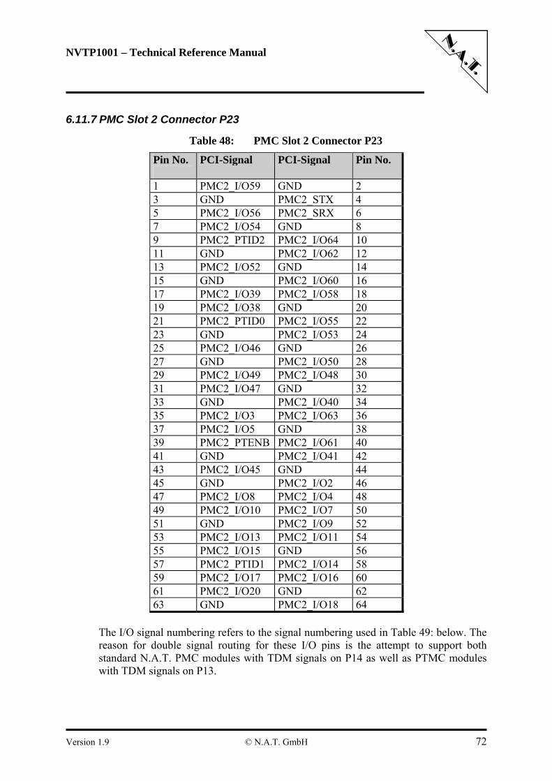
NVTP1001 – Technical Reference Manual
6.11.7 PMC Slot 2 Connector P23
Table 48: PMC Slot 2 Connector P23
Pin No.
PCI-Signal PCI-Signal Pin No.
1 PMC2_I/O59 GND 2 3 GND PMC2_STX 4 5 PMC2_I/O56 PMC2_SRX 6 7 PMC2_I/O54 GND 8 9 PMC2_PTID2 PMC2_I/O64 10 11 GND PMC2_I/O62 12 13 PMC2_I/O52 GND 14 15 GND PMC2_I/O60 16 17 PMC2_I/O39 PMC2_I/O58 18 19 PMC2_I/O38 GND 20 21 PMC2_PTID0 PMC2_I/O55 22 23 GND PMC2_I/O53 24 25 PMC2_I/O46 GND 26 27 GND PMC2_I/O50 28 29 PMC2_I/O49 PMC2_I/O48 30 31 PMC2_I/O47 GND 32 33 GND PMC2_I/O40 34 35 PMC2_I/O3 PMC2_I/O63 36 37 PMC2_I/O5 GND 38 39 PMC2_PTENB PMC2_I/O61 40 41 GND PMC2_I/O41 42 43 PMC2_I/O45 GND 44 45 GND PMC2_I/O2 46 47 PMC2_I/O8 PMC2_I/O4 48 49 PMC2_I/O10 PMC2_I/O7 50 51 GND PMC2_I/O9 52 53 PMC2_I/O13 PMC2_I/O11 54 55 PMC2_I/O15 GND 56 57 PMC2_PTID1 PMC2_I/O14 58 59 PMC2_I/O17 PMC2_I/O16 60 61 PMC2_I/O20 GND 62 63 GND PMC2_I/O18 64
The I/O signal numbering refers to the signal numbering used in Table 49: below. The reason for double signal routing for these I/O pins is the attempt to support both standard N.A.T. PMC modules with TDM signals on P14 as well as PTMC modules with TDM signals on P13.
Version 1.9 © N.A.T. GmbH 72
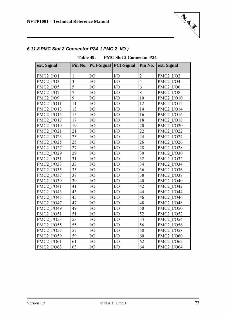
NVTP1001 – Technical Reference Manual
6.11.8 PMC Slot 2 Connector P24 ( PMC 2 I/O )
Table 49: PMC Slot 2 Connector P24
ext. Signal
Pin No. PCI-Signal PCI-Signal Pin No. ext. Signal
PMC2_I/O1 1 I/O I/O 2 PMC2_I/O2 PMC2_I/O3 3 I/O I/O 4 PMC2_I/O4 PMC2_I/O5 5 I/O I/O 6 PMC2_I/O6 PMC2_I/O7 7 I/O I/O 8 PMC2_I/O8 PMC2_I/O9 9 I/O I/O 10 PMC2_I/O10 PMC2_I/O11 11 I/O I/O 12 PMC2_I/O12 PMC2_I/O13 13 I/O I/O 14 PMC2_I/O14 PMC2_I/O15 15 I/O I/O 16 PMC2_I/O16 PMC2_I/O17 17 I/O I/O 18 PMC2_I/O18 PMC2_I/O19 19 I/O I/O 20 PMC2_I/O20 PMC2_I/O21 21 I/O I/O 22 PMC2_I/O22 PMC2_I/O23 23 I/O I/O 24 PMC2_I/O24 PMC2_I/O25 25 I/O I/O 26 PMC2_I/O26 PMC2_I/O27 27 I/O I/O 28 PMC2_I/O28 PMC2_I/O29 29 I/O I/O 30 PMC2_I/O30 PMC2_I/O31 31 I/O I/O 32 PMC2_I/O32 PMC2_I/O33 33 I/O I/O 34 PMC2_I/O34 PMC2_I/O35 35 I/O I/O 36 PMC2_I/O36 PMC2_I/O37 37 I/O I/O 38 PMC2_I/O38 PMC2_I/O39 39 I/O I/O 40 PMC2_I/O40 PMC2_I/O41 41 I/O I/O 42 PMC2_I/O42 PMC2_I/O43 43 I/O I/O 44 PMC2_I/O44 PMC2_I/O45 45 I/O I/O 46 PMC2_I/O46 PMC2_I/O47 47 I/O I/O 48 PMC2_I/O48 PMC2_I/O49 49 I/O I/O 50 PMC2_I/O50 PMC2_I/O51 51 I/O I/O 52 PMC2_I/O52 PMC2_I/O53 53 I/O I/O 54 PMC2_I/O54 PMC2_I/O55 55 I/O I/O 56 PMC2_I/O56 PMC2_I/O57 57 I/O I/O 58 PMC2_I/O58 PMC2_I/O59 59 I/O I/O 60 PMC2_I/O60 PMC2_I/O61 61 I/O I/O 62 PMC2_I/O62 PMC2_I/O63 63 I/O I/O 64 PMC2_I/O64
Version 1.9 © N.A.T. GmbH 73
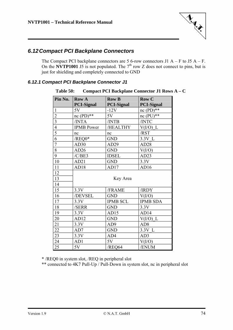
NVTP1001 – Technical Reference Manual
6.12 Compact PCI Backplane Connectors
The Compact PCI backplane connectors are 5 6-row connectors J1 A – F to J5 A – F. On the NVTP1001 J5 is not populated. The 7th row Z does not connect to pins, but is just for shielding and completely connected to GND
6.12.1 Compact PCI Backplane Connector J1
Table 50: Compact PCI Backplane Connector J1 Rows A – C
Pin No.
Row A PCI-Signal
Row B PCI-Signal
Row C PCI-Signal
1 5V -12V nc (PD)** 2 nc (PD)** 5V nc (PU)** 3 /INTA /INTB /INTC 4 IPMB Power /HEALTHY V(I/O)_L 5 nc nc /RST 6 /REQ0* GND 3.3V_L 7 AD30 AD29 AD28 8 AD26 GND V(I/O) 9 /C/BE3 IDSEL AD23 10 AD21 GND 3.3V 11 AD18 AD17 AD16 12 13 14
Key Area
15 3.3V /FRAME /IRDY 16 /DEVSEL GND V(I/O) 17 3.3V IPMB SCL IPMB SDA 18 /SERR GND 3.3V 19 3.3V AD15 AD14 20 AD12 GND V(I/O)_L 21 3.3V AD9 AD8 22 AD7 GND 3.3V_L 23 3.3V AD4 AD3 24 AD1 5V V(I/O) 25 5V /REQ64 /ENUM
* /REQ0 in system slot, /REQ in peripheral slot ** connected to 4K7 Pull-Up / Pull-Down in system slot, nc in peripheral slot
Version 1.9 © N.A.T. GmbH 74
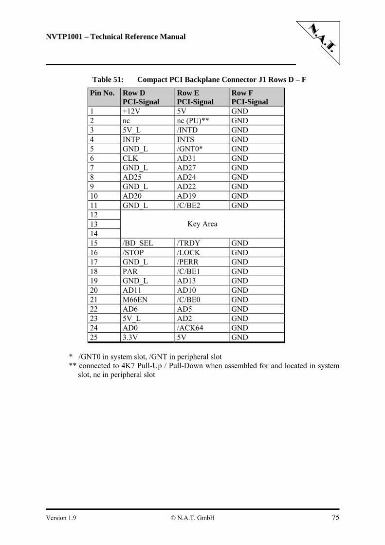
NVTP1001 – Technical Reference Manual
Table 51: Compact PCI Backplane Connector J1 Rows D – F
Pin No.
Row D PCI-Signal
Row E PCI-Signal
Row F PCI-Signal
1 +12V 5V GND 2 nc nc (PU)** GND 3 5V_L /INTD GND 4 INTP INTS GND 5 GND_L /GNT0* GND 6 CLK AD31 GND 7 GND_L AD27 GND 8 AD25 AD24 GND 9 GND_L AD22 GND 10 AD20 AD19 GND 11 GND_L /C/BE2 GND 12 13 14
Key Area
15 /BD_SEL /TRDY GND 16 /STOP /LOCK GND 17 GND_L /PERR GND 18 PAR /C/BE1 GND 19 GND_L AD13 GND 20 AD11 AD10 GND 21 M66EN /C/BE0 GND 22 AD6 AD5 GND 23 5V_L AD2 GND 24 AD0 /ACK64 GND 25 3.3V 5V GND
* /GNT0 in system slot, /GNT in peripheral slot ** connected to 4K7 Pull-Up / Pull-Down when assembled for and located in system
slot, nc in peripheral slot
Version 1.9 © N.A.T. GmbH 75
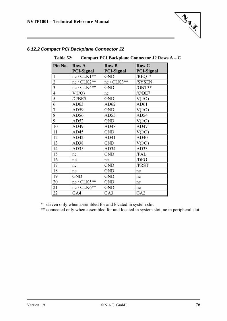
NVTP1001 – Technical Reference Manual
6.12.2 Compact PCI Backplane Connector J2
Table 52: Compact PCI Backplane Connector J2 Rows A – C
Pin No.
Row A PCI-Signal
Row B PCI-Signal
Row C PCI-Signal
1 nc / CLK1** GND /REQ1* 2 nc / CLK2** nc / CLK3** /SYSEN 3 nc / CLK4** GND /GNT3* 4 V(I/O) nc /C/BE7 5 /C/BE5 GND V(I/O) 6 AD63 AD62 AD61 7 AD59 GND V(I/O) 8 AD56 AD55 AD54 9 AD52 GND V(I/O) 10 AD49 AD48 AD47 11 AD45 GND V(I/O) 12 AD42 AD41 AD40 13 AD38 GND V(I/O) 14 AD35 AD34 AD33 15 nc GND /FAL 16 nc nc /DEG 17 nc GND /PRST 18 nc GND nc 19 GND GND nc 20 nc / CLK5** GND nc 21 nc / CLK6** GND nc 22 GA4 GA3 GA2
* driven only when assembled for and located in system slot ** connected only when assembled for and located in system slot, nc in peripheral slot
Version 1.9 © N.A.T. GmbH 76
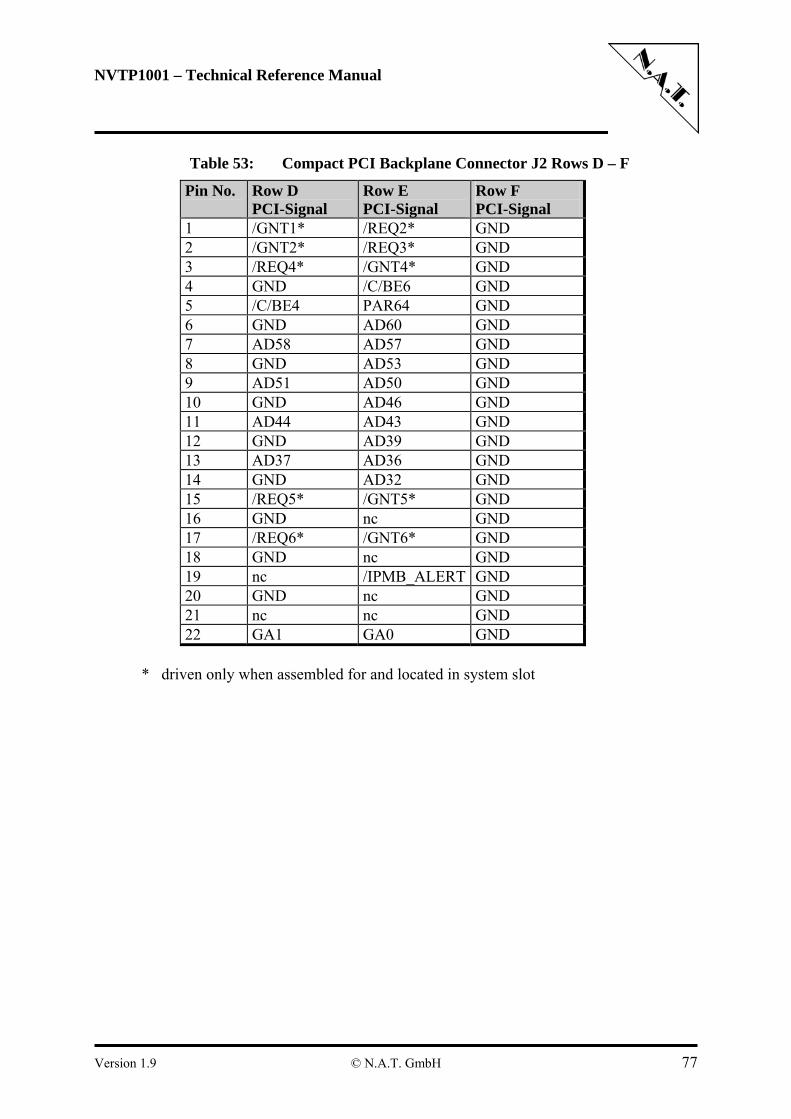
NVTP1001 – Technical Reference Manual
Table 53: Compact PCI Backplane Connector J2 Rows D – F
Pin No.
Row D PCI-Signal
Row E PCI-Signal
Row F PCI-Signal
1 /GNT1* /REQ2* GND 2 /GNT2* /REQ3* GND 3 /REQ4* /GNT4* GND 4 GND /C/BE6 GND 5 /C/BE4 PAR64 GND 6 GND AD60 GND 7 AD58 AD57 GND 8 GND AD53 GND 9 AD51 AD50 GND 10 GND AD46 GND 11 AD44 AD43 GND 12 GND AD39 GND 13 AD37 AD36 GND 14 GND AD32 GND 15 /REQ5* /GNT5* GND 16 GND nc GND 17 /REQ6* /GNT6* GND 18 GND nc GND 19 nc /IPMB_ALERT GND 20 GND nc GND 21 nc nc GND 22 GA1 GA0 GND
* driven only when assembled for and located in system slot
Version 1.9 © N.A.T. GmbH 77
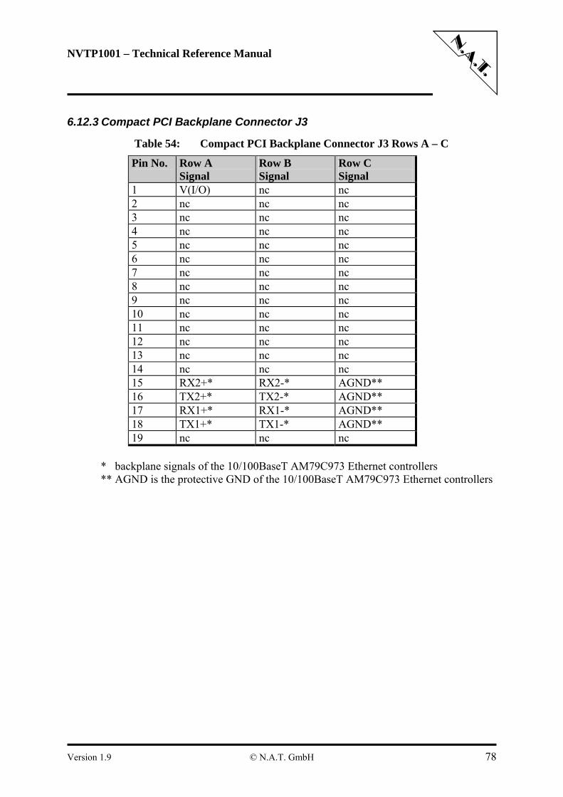
NVTP1001 – Technical Reference Manual
6.12.3 Compact PCI Backplane Connector J3
Table 54: Compact PCI Backplane Connector J3 Rows A – C
Pin No.
Row A Signal
Row B Signal
Row C Signal
1 V(I/O) nc nc 2 nc nc nc 3 nc nc nc 4 nc nc nc 5 nc nc nc 6 nc nc nc 7 nc nc nc 8 nc nc nc 9 nc nc nc 10 nc nc nc 11 nc nc nc 12 nc nc nc 13 nc nc nc 14 nc nc nc 15 RX2+* RX2-* AGND** 16 TX2+* TX2-* AGND** 17 RX1+* RX1-* AGND** 18 TX1+* TX1-* AGND** 19 nc nc nc
* backplane signals of the 10/100BaseT AM79C973 Ethernet controllers ** AGND is the protective GND of the 10/100BaseT AM79C973 Ethernet controllers
Version 1.9 © N.A.T. GmbH 78
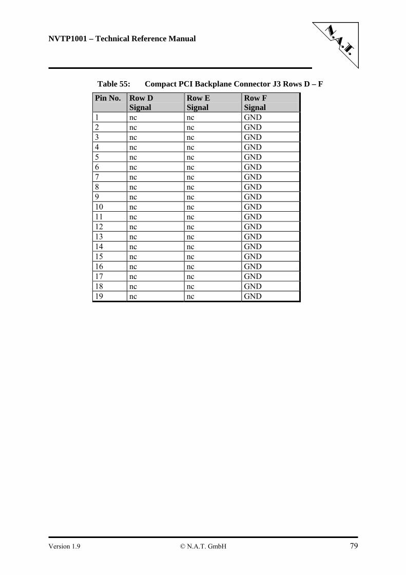
NVTP1001 – Technical Reference Manual
Table 55: Compact PCI Backplane Connector J3 Rows D – F
Pin No.
Row D Signal
Row E Signal
Row F Signal
1 nc nc GND 2 nc nc GND 3 nc nc GND 4 nc nc GND 5 nc nc GND 6 nc nc GND 7 nc nc GND 8 nc nc GND 9 nc nc GND 10 nc nc GND 11 nc nc GND 12 nc nc GND 13 nc nc GND 14 nc nc GND 15 nc nc GND 16 nc nc GND 17 nc nc GND 18 nc nc GND 19 nc nc GND
Version 1.9 © N.A.T. GmbH 79
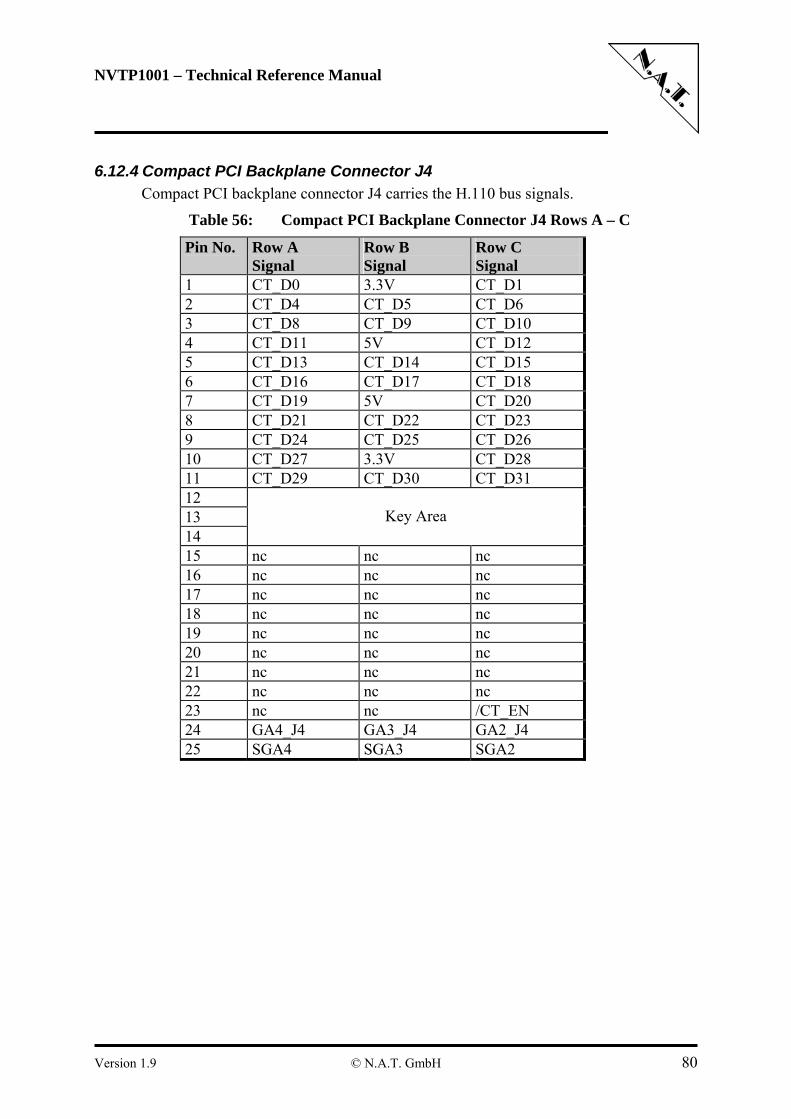
NVTP1001 – Technical Reference Manual
6.12.4 Compact PCI Backplane Connector J4 Compact PCI backplane connector J4 carries the H.110 bus signals.
Table 56: Compact PCI Backplane Connector J4 Rows A – C
Pin No.
Row A Signal
Row B Signal
Row C Signal
1 CT_D0 3.3V CT_D1 2 CT_D4 CT_D5 CT_D6 3 CT_D8 CT_D9 CT_D10 4 CT_D11 5V CT_D12 5 CT_D13 CT_D14 CT_D15 6 CT_D16 CT_D17 CT_D18 7 CT_D19 5V CT_D20 8 CT_D21 CT_D22 CT_D23 9 CT_D24 CT_D25 CT_D26 10 CT_D27 3.3V CT_D28 11 CT_D29 CT_D30 CT_D31 12 13 14
Key Area
15 nc nc nc 16 nc nc nc 17 nc nc nc 18 nc nc nc 19 nc nc nc 20 nc nc nc 21 nc nc nc 22 nc nc nc 23 nc nc /CT_EN 24 GA4_J4 GA3_J4 GA2_J4 25 SGA4 SGA3 SGA2
Version 1.9 © N.A.T. GmbH 80
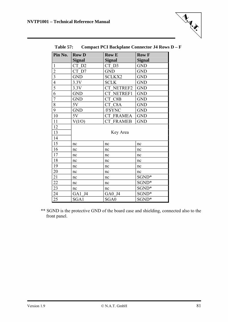
NVTP1001 – Technical Reference Manual
Table 57: Compact PCI Backplane Connector J4 Rows D – F
Pin No.
Row D Signal
Row E Signal
Row F Signal
1 CT_D2 CT_D3 GND 2 CT_D7 GND GND 3 GND SCLKX2 GND 4 3.3V SCLK GND 5 3.3V CT_NETREF2 GND 6 GND CT_NETREF1 GND 7 GND CT_C8B GND 8 5V CT_C8A GND 9 GND /FSYNC GND 10 5V CT_FRAMEA GND 11 V(I/O) CT_FRAMEB GND 12 13 14
Key Area
15 nc nc nc 16 nc nc nc 17 nc nc nc 18 nc nc nc 19 nc nc nc 20 nc nc nc 21 nc nc SGND* 22 nc nc SGND* 23 nc nc SGND* 24 GA1_J4 GA0_J4 SGND* 25 SGA1 SGA0 SGND*
** SGND is the protective GND of the board case and shielding, connected also to the
front panel.
Version 1.9 © N.A.T. GmbH 81
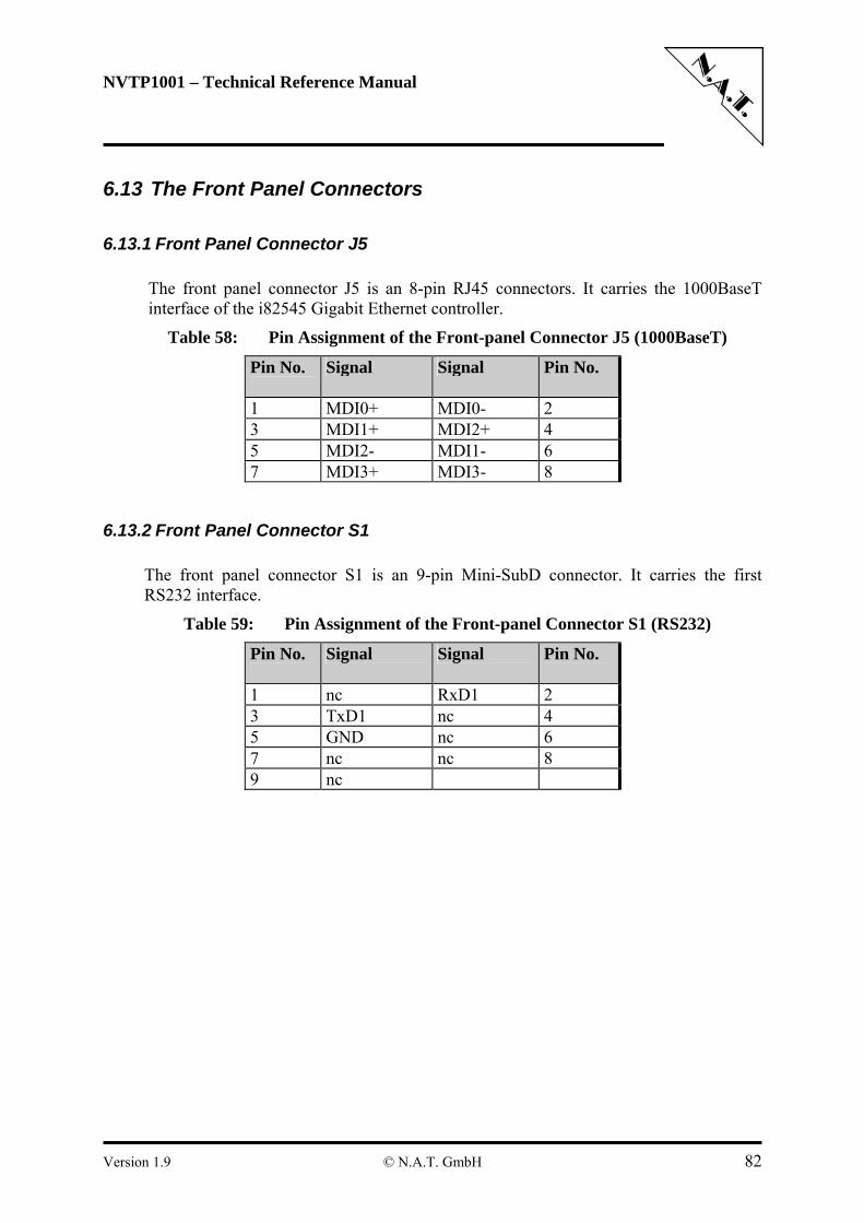
NVTP1001 – Technical Reference Manual
6.13 The Front Panel Connectors
6.13.1 Front Panel Connector J5
The front panel connector J5 is an 8-pin RJ45 connectors. It carries the 1000BaseT interface of the i82545 Gigabit Ethernet controller.
Table 58: Pin Assignment of the Front-panel Connector J5 (1000BaseT)
Pin No.
Signal Signal Pin No.
1 MDI0+ MDI0- 2 3 MDI1+ MDI2+ 4 5 MDI2- MDI1- 6 7 MDI3+ MDI3- 8
6.13.2 Front Panel Connector S1 The front panel connector S1 is an 9-pin Mini-SubD connector. It carries the first RS232 interface.
Table 59: Pin Assignment of the Front-panel Connector S1 (RS232)
Pin No.
Signal Signal Pin No.
1 nc RxD1 2 3 TxD1 nc 4 5 GND nc 6 7 nc nc 8 9 nc
Version 1.9 © N.A.T. GmbH 82
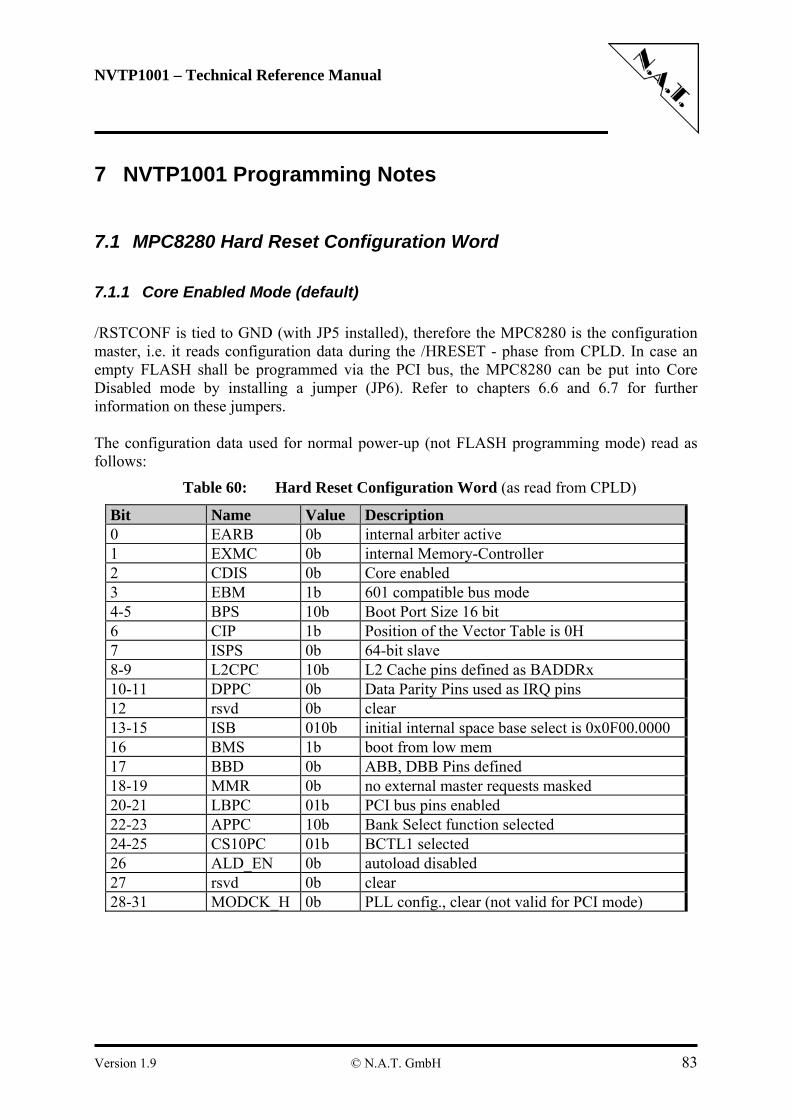
NVTP1001 – Technical Reference Manual
7 NVTP1001 Programming Notes
7.1 MPC8280 Hard Reset Configuration Word
7.1.1 Core Enabled Mode (default) /RSTCONF is tied to GND (with JP5 installed), therefore the MPC8280 is the configuration master, i.e. it reads configuration data during the /HRESET - phase from CPLD. In case an empty FLASH shall be programmed via the PCI bus, the MPC8280 can be put into Core Disabled mode by installing a jumper (JP6). Refer to chapters 6.6 and 6.7 for further information on these jumpers. The configuration data used for normal power-up (not FLASH programming mode) read as follows:
Table 60: Hard Reset Configuration Word (as read from CPLD)
Bit Name Value Description 0 EARB 0b internal arbiter active 1 EXMC 0b internal Memory-Controller 2 CDIS 0b Core enabled 3 EBM 1b 601 compatible bus mode 4-5 BPS 10b Boot Port Size 16 bit 6 CIP 1b Position of the Vector Table is 0H 7 ISPS 0b 64-bit slave 8-9 L2CPC 10b L2 Cache pins defined as BADDRx 10-11 DPPC 0b Data Parity Pins used as IRQ pins 12 rsvd 0b clear 13-15 ISB 010b initial internal space base select is 0x0F00.0000 16 BMS 1b boot from low mem 17 BBD 0b ABB, DBB Pins defined 18-19 MMR 0b no external master requests masked 20-21 LBPC 01b PCI bus pins enabled 22-23 APPC 10b Bank Select function selected 24-25 CS10PC 01b BCTL1 selected 26 ALD_EN 0b autoload disabled 27 rsvd 0b clear 28-31 MODCK_H 0b PLL config., clear (not valid for PCI mode)
Version 1.9 © N.A.T. GmbH 83
NVTP1001 – Technical Reference Manual
7.1.2 Core Disabled Mode (FLASH programming mode) In case of FLASH programming mode the ALD_EN bit in the Hard Reset Configuration Word is set to 1b (autoload function, bit 26). In this case, the MPC8280 reads additional information from the CPLD, in order to do some basic register setup. The start address of this block of additional information is always read from address 0x04. The CPLD sets the block start address to be 0x80. The following register setup is performed in core disabled mode for FLASH programming mode:
- SYPCR is written 0xFFFF.FF00 in order to disable the watchdog - PCI Sub System Device ID is written 0x0603, which is used as N.A.T. board
identification code for the NVTP1001 - PCI Inbound Comparison Mask Register PICMR1 is written to 0x800F.FFE0 in order
to request 128KB of PCI memory space for programming mode - PCI Bus Function register is written 0x0 in order to clear CFG_LOCK and enable PCI
access to the bridge - register OR0 is written 0xFE00.0E84, which reduces the no. of waitstates to 8 - register BR0 is written 0xFE00.1001, which sets the port size to 16 bits data width or
to 8 bits data width, depending on the setting of JP7 (refer to chapter 6.8)
With these settings FLASH programming via the PCI bus can be performed with the CPU core in disabled mode. After the FLASH programming is completed, jumper JP6 has to be removed again, in order to allow core enabled boot whith the next power-cycle.
Version 1.9 © N.A.T. GmbH 84
NVTP1001 – Technical Reference Manual
7.2 Recommended General Control Register Setup
7.2.1 Register-Setup of the System Clock Control Register (SCCR) SCCR Bit Name Value Description Bit 0-28 rsvd 0b clear Bit 29 CLPD 0b CPM does not enter low power mode Bit 30-31 DFBRG 0b division factor of 4
7.2.2 Register-Setup of the System Protection Control Register (SYPCR) SYPCR Bit Name Value Description Bit 0-15 SWTC 0xFFFF software watchdog timer count Bit 16-23 BMT 0xFF bus monitor timing Bit 24 PBME 1b 60x bus monitor enabled Bit 25 LBME 1b local bus monitor enabled Bit 26-28 rsvd 0b clear Bit 29 SWE 0b software watchdog disabled Bit 30 SWRI 1b watchdog and bus monitors cause soft reset Bit 31 SWP 1b software watchdog timer is prescaled
7.2.3 Register-Setup of the Bus Configurations Register (BCR) BCR Bit Name Value Description Bit 0 EBM 1b external bus mode 60x mode Bit 1-3 APD 011b address phase delay Bit 4 L2C 0b no secondary cache Bit 5-7 L2D 0b hit delay, not applicable Bit 8 PLDP 0b pipeline max. depth Bit 9 EAV 1b full address on 60x bus Bit 10-11 rsvd 0b clear Bit 12 ETM 0b compatibility mode enable, disabled Bit 13 LETM 0b local compatibility mode enable, disabled Bit 14 EPAR 0b even parity Bit 15 LEPAR 0b local even parity Bit 16-18 NPQM 111b non PowerQUICC master Bit 19-20 rsvd 0b clear Bit 21 EXDD 0b external master delay enabled Bit 22-26 rsvd 0b clear Bit 27 ISPS 0b internal space port size is 64 bit Bit 28-31 rsvd 0b clear
Version 1.9 © N.A.T. GmbH 85
NVTP1001 – Technical Reference Manual
7.2.4 Register-Setup of the 60x Bus Arbiter Configurations Register (PPC_ACR)
P_ACR Bit Name Value Description Bit 0-1 rsvd 0b clear Bit 2 DBGD 0b DBG asserted with TS Bit 3 EARB 0b internal bus arbitration Bit 4-7 PRKM 0010b parking master is CPM low request level
7.2.5 Register-Setup of the Local Bus Arbiter Configurations Register (LCL_ACR)
L_ACR Bit Name Value Description Bit 0 rsvd 0b clear Bit 2 DBGD 0b DBG asserted with TS Bit 3 EARB 0b internal bus arbitration Bit 4-7 PRKM 0110b parking master is internal core
7.2.6 Register-Setup of the SIU Module Configurations Register (SIUMCR) SIUMCR Bit Name Value Description Bit 0 BBD 0b ABB, DBB selected Bit 1 ESE 0b IRQ1 selected Bit 2 PBSE 0b parity byte select disabled Bit 3 CDIS 0b core enabled Bit 4-5 DPPC 00b IRQ function selected Bit 6-7 L2CPC 10b BADDRx selected Bit 8-9 LBPC 0b local bus pins selected Bit 10-11 APPC 10b BNKSEL function enabled Bit 12-13 CS10PC 00b CS10 selected Bit 14-15 BCTLC 0b buffer control Bit 16-17 MMR 0b no masking of bus requests Bit 18 LPBSE 0b local parity disabled Bit 19-31 rsvd 0b clear
Version 1.9 © N.A.T. GmbH 86
NVTP1001 – Technical Reference Manual
7.2.7 Register-Setup of the 60x Bus Transfer Status/Control Register (TESCR1)
SCCR Bit Name Value Description Bit 0-16 not used 0b clear Bit 17 DMD 1b all data errors disabled Bit 18-31 not used 0b clear
7.2.8 Register-Setup of the Local Bus Transfer Status/Control Register (L_TESCR1)
SCCR Bit Name Value Description Bit 0-16 not used 0b clear Bit 17 DMD 1b all data parity errors disabled Bit 18-31 not used 0b clear
Version 1.9 © N.A.T. GmbH 87
NVTP1001 – Technical Reference Manual
7.3 Recommended Register Setup of the Memory Controller:
7.3.1 Base Registers BRx: The base addresses given in the description below are the ones chosen for the OK1 and VxWorks implementations for the NVTP1001. They may be altered to suit the user’s needs. BRx: Base Register of the corresponding CS; CS settings as described in Table 3 above. BR0 Bit Name Value Description Bit 0-16 BA <address> base address <address>, FLASH Bit 17-18 rsvd 0b clear Bit 19-20 PS 01b port size 8 bit (depends on which FLASH is selected as
boot FLASH) Bit 21-22 DECC 0b ECC disabled Bit 23 WP 0b R/W Bit 24-26 MS 0b default, 601 bus Bit 27 EMEMC 0b memory controller active Bit 28-29 ATOM 0b no atomic operations Bit 30 DR 0b no data pipelining Bit 31 V 1b valid bank BR1 Bit Name Value Description Bit 0-16 BA <address> base address <address>, FLASH Bit 17-18 rsvd 0b clear Bit 19-20 PS 10b port size 16 bit (depends on which FLASH is selected as
boot FLASH) Bit 21-22 DECC 0b ECC disabled Bit 23 WP 0b R/W Bit 24-26 MS 0b default, 601 bus Bit 27 EMEMC 0b memory controller active Bit 28-29 ATOM 0b no atomic operations Bit 30 DR 0b no data pipelining Bit 31 V 1b valid bank
Version 1.9 © N.A.T. GmbH 88
NVTP1001 – Technical Reference Manual
BR2 Bit Name Value Description Bit 0-16 BA <address> base address <address>, SDRAM CS0 Bit 17-18 rsvd 0b clear Bit 19-20 PS 0b port size 64 bit Bit 21-22 DECC 0b ECC disabled Bit 23 WP 0b R/W Bit 24-26 MS 010b SDRAM, 601 bus Bit 27 EMEMC 0b memory controller active Bit 28-29 ATOM 0b no atomic operations Bit 30 DR 0b no data pipelining Bit 31 V 1b valid bank The settings of BR2 and BR3 are suitable for the default 32 MB SODIMM module installed. The default module uses only one CS, hence the programming of BR3/OR3 is not necessary. BR3 Bit Name Value Description Bit 0-16 BA <address> base address <address>, SDRAM CS1 Bit 17-18 rsvd 0b clear Bit 19-20 PS 0b port size 64 bit Bit 21-22 DECC 0b ECC disabled Bit 23 WP 0b R/W Bit 24-26 MS 010b SDRAM, 601 bus Bit 27 EMEMC 0b memory controller active Bit 28-29 ATOM 0b no atomic operations Bit 30 DR 0b no data pipelining Bit 31 V 0b invalid bank BR4 Bit Name Value Description Bit 0-16 BA <address> base address <address>, control/status register Bit 17-18 rsvd 0b clear Bit 19-20 PS 01b port size 8 bit Bit 21-22 DECC 0b ECC disabled Bit 23 WP 0b R/W Bit 24-26 MS 0b default, 601 bus Bit 27 EMEMC 0b memory controller active Bit 28-29 ATOM 0b no atomic operations Bit 30 DR 0b no data pipelining Bit 31 V 1b valid bank
Version 1.9 © N.A.T. GmbH 89
NVTP1001 – Technical Reference Manual
BR5 Bit Name Value Description Bit 0-16 BA <address> base address <address>, FPGA Bit 17-18 rsvd 0b clear Bit 19-20 PS 01b port size 8 bit Bit 21-22 DECC 0b ECC disabled Bit 23 WP 0b R/W Bit 24-26 MS 0b default, 601 bus Bit 27 EMEMC 0b memory controller active Bit 28-29 ATOM 0b no atomic operations Bit 30 DR 0b no data pipelining Bit 31 V 1b valid bank BR6-11 Bit Name Value Description Bit 0-16 BA <address> base address <address>, SRAM
(each CSSRAM covers a 256 kByte SRAM area, check with Table 3 for details)
Bit 17-18 rsvd 0b clear Bit 19-20 PS 11b port size 32 bit Bit 21-22 DECC 0b ECC disabled Bit 23 WP 0b R/W Bit 24-26 MS 001b GPCM, local bus Bit 27 EMEMC 0b memory controller active Bit 28-29 ATOM 0b no atomic operations Bit 30 DR 0b no data pipelining Bit 31 V 1b valid bank
Version 1.9 © N.A.T. GmbH 90
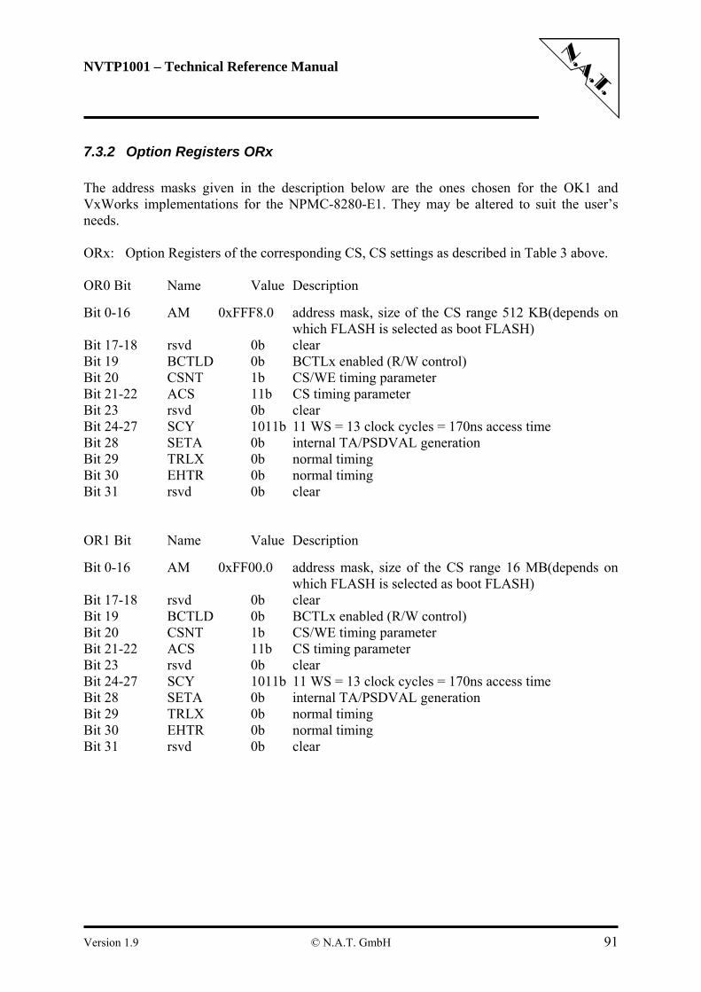
NVTP1001 – Technical Reference Manual
7.3.2 Option Registers ORx The address masks given in the description below are the ones chosen for the OK1 and VxWorks implementations for the NPMC-8280-E1. They may be altered to suit the user’s needs. ORx: Option Registers of the corresponding CS, CS settings as described in Table 3 above. OR0 Bit Name Value Description Bit 0-16 AM 0xFFF8.0 address mask, size of the CS range 512 KB(depends on
which FLASH is selected as boot FLASH) Bit 17-18 rsvd 0b clear Bit 19 BCTLD 0b BCTLx enabled (R/W control) Bit 20 CSNT 1b CS/WE timing parameter Bit 21-22 ACS 11b CS timing parameter Bit 23 rsvd 0b clear Bit 24-27 SCY 1011b 11 WS = 13 clock cycles = 170ns access time Bit 28 SETA 0b internal TA/PSDVAL generation Bit 29 TRLX 0b normal timing Bit 30 EHTR 0b normal timing Bit 31 rsvd 0b clear OR1 Bit Name Value Description Bit 0-16 AM 0xFF00.0 address mask, size of the CS range 16 MB(depends on
which FLASH is selected as boot FLASH) Bit 17-18 rsvd 0b clear Bit 19 BCTLD 0b BCTLx enabled (R/W control) Bit 20 CSNT 1b CS/WE timing parameter Bit 21-22 ACS 11b CS timing parameter Bit 23 rsvd 0b clear Bit 24-27 SCY 1011b 11 WS = 13 clock cycles = 170ns access time Bit 28 SETA 0b internal TA/PSDVAL generation Bit 29 TRLX 0b normal timing Bit 30 EHTR 0b normal timing Bit 31 rsvd 0b clear
Version 1.9 © N.A.T. GmbH 91
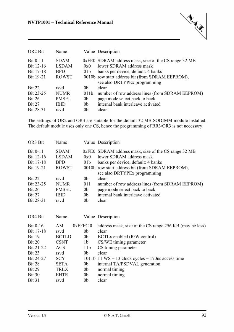
NVTP1001 – Technical Reference Manual
OR2 Bit Name Value Description Bit 0-11 SDAM 0xFE0 SDRAM address mask, size of the CS range 32 MB Bit 12-16 LSDAM 0x0 lower SDRAM address mask Bit 17-18 BPD 01b banks per device, default: 4 banks Bit 19-21 ROWST 0010b row start address bit (from SDRAM EEPROM), see also DRTYPEx programming Bit 22 rsvd 0b clear Bit 23-25 NUMR 011b number of row address lines (from SDRAM EEPROM) Bit 26 PMSEL 0b page mode select back to back Bit 27 IBID 0b internal bank interleave activated Bit 28-31 rsvd 0b clear The settings of OR2 and OR3 are suitable for the default 32 MB SODIMM module installed. The default module uses only one CS, hence the programming of BR3/OR3 is not necessary. OR3 Bit Name Value Description Bit 0-11 SDAM 0xFE0 SDRAM address mask, size of the CS range 32 MB Bit 12-16 LSDAM 0x0 lower SDRAM address mask Bit 17-18 BPD 01b banks per device, default: 4 banks Bit 19-21 ROWST 0010b row start address bit (from SDRAM EEPROM), see also DRTYPEx programming Bit 22 rsvd 0b clear Bit 23-25 NUMR 011 number of row address lines (from SDRAM EEPROM) Bit 26 PMSEL 0b page mode select back to back Bit 27 IBID 0b internal bank interleave activated Bit 28-31 rsvd 0b clear OR4 Bit Name Value Description Bit 0-16 AM 0xFFFC.0 address mask, size of the CS range 256 KB (may be less) Bit 17-18 rsvd 0b clear Bit 19 BCTLD 0b BCTLx enabled (R/W control) Bit 20 CSNT 1b CS/WE timing parameter Bit 21-22 ACS 11b CS timing parameter Bit 23 rsvd 0b clear Bit 24-27 SCY 1011b 11 WS = 13 clock cycles = 170ns access time Bit 28 SETA 0b internal TA/PSDVAL generation Bit 29 TRLX 0b normal timing Bit 30 EHTR 0b normal timing Bit 31 rsvd 0b clear
Version 1.9 © N.A.T. GmbH 92
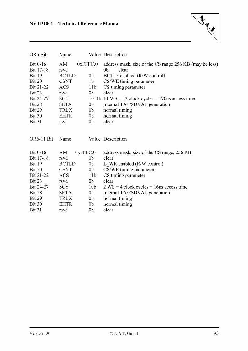
NVTP1001 – Technical Reference Manual
OR5 Bit Name Value Description Bit 0-16 AM 0xFFFC.0 address mask, size of the CS range 256 KB (may be less) Bit 17-18 rsvd 0b clear Bit 19 BCTLD 0b BCTLx enabled (R/W control) Bit 20 CSNT 1b CS/WE timing parameter Bit 21-22 ACS 11b CS timing parameter Bit 23 rsvd 0b clear Bit 24-27 SCY 1011b 11 WS = 13 clock cycles = 170ns access time Bit 28 SETA 0b internal TA/PSDVAL generation Bit 29 TRLX 0b normal timing Bit 30 EHTR 0b normal timing Bit 31 rsvd 0b clear OR6-11 Bit Name Value Description Bit 0-16 AM 0xFFFC.0 address mask, size of the CS range, 256 KB Bit 17-18 rsvd 0b clear Bit 19 BCTLD 0b L_WR enabled (R/W control) Bit 20 CSNT 0b CS/WE timing parameter Bit 21-22 ACS 11b CS timing parameter Bit 23 rsvd 0b clear Bit 24-27 SCY 10b 2 WS = 4 clock cycles = 16ns access time Bit 28 SETA 0b internal TA/PSDVAL generation Bit 29 TRLX 0b normal timing Bit 30 EHTR 0b normal timing Bit 31 rsvd 0b clear
Version 1.9 © N.A.T. GmbH 93
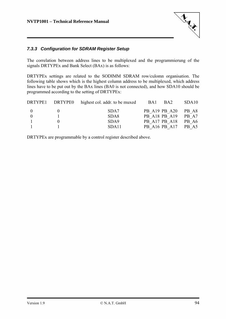
NVTP1001 – Technical Reference Manual
7.3.3 Configuration for SDRAM Register Setup The correlation between address lines to be multiplexed and the programmierung of the signals DRTYPEx and Bank Select (BAx) is as follows: DRTYPEx settings are related to the SODIMM SDRAM row/culomn organisation. The following table shows which is the highest column address to be multiplexed, which address lines have to be put out by the BAx lines (BA0 is not connected), and how SDA10 should be programmed according to the setting of DRTYPEx: DRTYPE1 DRTYPE0 highest col. addr. to be muxed BA1 BA2 SDA10 0 0 SDA7 PB_A19 PB_A20 PB_A8 0 1 SDA8 PB_A18 PB_A19 PB_A7 1 0 SDA9 PB_A17 PB_A18 PB_A6 1 1 SDA11 PB_A16 PB_A17 PB_A5 DRTYPEx are programmable by a control register described above.
Version 1.9 © N.A.T. GmbH 94
NVTP1001 – Technical Reference Manual
7.3.4 SDRAM Mode Register PSDMRx PSDMR Bit Name Value Description Bit 0 PBI 1b page-based Interleave Bit 1 RFEN 1b refresh necessary Bit 2-4 OP 000b SDRAM operation Bit 5-7 SDAM 010b depending on SDRAM parameters and on DRTYPEx Bit 8-10 BSMA 110b depending on SDRAM parameters and on DRTYPEx Bit 11-13 SDA10 010b depending on SDRAM parameters and on DRTYPEx (see table below) Bit 14-16 RFRC 110b depending on SDRAM parameters Bit 17-19 PRETOACT 100b depending on SDRAM parameters Bit 20-22 ACTTORW 100b depending on SDRAM parameters Bit 23 BL 0b burst length is 4 Bit 24-25 LDOTOPRE 10b depending on SDRAM parameters Bit 26-27 WRC 11b depending on SDRAM parameters Bit 28 EAMUX 1b external address multiplexer Bit 29 BUFCMD 0b normal timing Bit 30-31 CL 10b depending on SDRAM parameters
7.3.5 PSRT 60x Bus-Assigned SDRAM Refresh Timer Register PSRT Bit Name Value Description Bit 0-7 PSRT 0x20 timer value of 32 for prescaler 64
7.3.6 MPTPR Memory Refresh Timer Prescaler Register MPTPR Bit Name Value Description Bit 0-7 PSRT 0x40 prescaler value 64 Bit 8-15 rsvd 0b clear
7.3.7 UPM Machine Mode Register MxMR UPMs are not used in this version. If UPMs are to be used, take the restriction of bus frequency and UPM usage for some MPC8280 masks and versions into account.
Version 1.9 © N.A.T. GmbH 95
NVTP1001 – Technical Reference Manual
7.4 Setup of the Serial Interfaces
7.4.1 RS232 Interface on the Front Panel Connector S1 The programming of the RS232 serial interface is performed through channel SMC1 of the MPC8280 – internal CPM.
7.4.2 RS232 Debug Interface on JP9 In order to program the RS232 serial debug interface it is necessary to route the appropriate MPC8280 port pins to connector JP9. This is done by programming the Central Switching Resource in a way, that either one of the 4 SCC’s, or SMC2 is routed to the connector pins. Which one will be appropriate depends on the application the Central Switching Resource is programmed to fulfill, as different CPU port pins are used for different applications. Refer to chapter 7.9 for details on the programming and pin layout of the Central Switching Resource.
7.4.3 I2C Interface The I2C interface is connected to CPLD pins programmable by a control register described above. The EEPROM on the SDRAM SODIMM module has address 0 and should be read and analyzed before initialising the SDRAM machine, in order to be able to setup the SDRAM machine, the external logik (DRTYPEx for U25), and the SDRAMs themselves. The address of the EEPROM U24 used for storage of board-specific parameters is 4. The control code (1st 4 bits of the address) for the 24Cxx EEPROM is 1010b, which results in address 0x50 for the SODIMM EEPROM and in address 0x54 for the parameter EEPROM.
Version 1.9 © N.A.T. GmbH 96
NVTP1001 – Technical Reference Manual
7.5 Definition of the Multi-Function Pins
Table 61: Definition of the Multi-Function Pins
Pin Name Pin Function on the NPMC-8280-E1 DBB/IRQ3 DBB DP(0-7)/misc. IRQx GBL/IRQ1 IRQ1, not used CI/BADDR29/IRQ2 BADDR29 WT/BADDR30/IRQ3 BADDR30 L2_HIT/IRQ4 L2_HIT, not used CPU_BG/BADDR31/IRQ5 BADDR31 CS10/BCTL1/DBG_DIS CS10 CS11/AP0 CS11 PWE(0-7)/PSDDQM(0-7)/PBS(0-7) PSDDQM(0-7) PSDA10/PGPL0 PSDA10 PSDWE/PGPL1 PSDWE POE/PSDRAS/PGPL2 PSDRAS PSDCAS/PGPL3 PSDCAS PGTA/PUPMWAIT/PGPL4/PPBS PGTA PSDAMUX/PGPL5 PSDAMUX LWE(0-3)/LSDDQM(0-3)/LBS(0-3) PCI LSDA10/LGPL0 PCI LSDWE/LGPL1 PCI LOE/LSDRAS/LGPL2 PCI LSDCAS/LGPL3 PCI LGTA/LUPWAIT/LGPL4/LPBS LGTA LSDAMUX/LGPL5 PCI L_A15/SMI PCI L_A17/CHKSTO_OUT PCI L_A27/CLKOUT PCI L_A28/CORE_SRESET PCI L_A31/DLLSYNC PCI L_CLDP(0-3) PCI IRQ0/NMIOUT IRQ0 IRQ7/INTOUT/APE INTOUT, not used Apx/TCx/BNKSELx BNKSELx
Version 1.9 © N.A.T. GmbH 97
NVTP1001 – Technical Reference Manual
7.6 Programming the PCI Bridges
7.6.1 Intel 21555 Bridge Programming The Intel 21555 Bridge, which bridges between the Compact PCI bus and the internal PCI bus 1, is initialized by two ways: Power-Up configuration and EEPROM load of setup information on various Reset conditions.
7.6.1.1 Intel 21555 Power-Up Configuration Power-Up configuration is done by pulling the data pins of the ROM interface to specific logic levels during Power-Up Reset. Details are found in the table below.
Table 62: Intel 21555 Power-Up Configuration
Data bit Function initialized to PR_AD7 cPCI bus central functions enabled/disabled* PR_AD6 PCI arbiter cPCI bus enabled/disabled* PR_AD5 S_CLK_O disabled PR_AD4 Sync Mode asynchronous PR_AD3 Primary Lockout Reset
Value configuration bit 0b
PR_AD2 none pulled high PR_AD1 PCI bus 1 64 bit enable enabled
* Setting depends on chosen assembly option for slot 1 functionality
7.6.1.2 Configuration by EEPROM Load When reset, the i21555 loads several registers from EEPROM, if available. On the NVTP1001, a 93LC66A serial EEPROM is connected to the serial ROM interface of the i21555. The following data is loaded (please consult the i21555 User’s Manual for a detailed description):
Table 63: i21555 EEPROM Configuration
Serial ROM Address
Hex Value
0x0 80 00 00 00 00 80 06 46 00 11 10 00 00 00 80 060x10 00 00 00 00 00 00 00 00 00 00 00 00 00 00 00 000x20 00 00 00 00 00 00 F1 1F 00 00 00 FF 00 00 00 FF0x30 00 08 00 00 18 02 7F 7F 06 80 00 00 00 00 00 000x40 00 40 00 FF 70 A5 10 00 03 06 00 00 01 00 00 000x50 00 00 00 00 00 00 00 00 FF FF FF FF FF FF FF FF
0x60-0xFF FF FF FF FF FF FF FF FF FF FF FF FF FF FF FF FF
Version 1.9 © N.A.T. GmbH 98
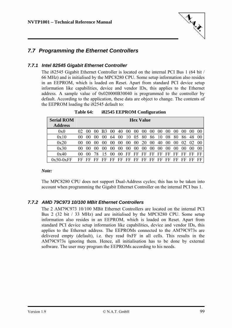
NVTP1001 – Technical Reference Manual
7.7 Programming the Ethernet Controllers
7.7.1 Intel 82545 Gigabit Ethernet Controller The i82545 Gigabit Ethernet Controller is located on the internal PCI Bus 1 (64 bit / 66 MHz) and is initialised by the MPC8280 CPU. Some setup information also resides in an EEPROM, which is loaded on Reset. Apart from standard PCI device setup information like capabilities, device and vendor IDs, this applies to the Ethernet address. A sample value of 0x020000B30040 is programmed to the controller by default. According to the application, these data are object to change. The contents of the EEPROM loading the i82545 default to:
Table 64: i82545 EEPROM Configuration
Serial ROM Address
Hex Value
0x0 02 00 00 B3 00 40 00 00 00 00 00 00 00 00 00 000x10 00 00 00 00 64 00 10 05 80 86 10 08 80 86 48 000x20 00 00 00 00 00 00 00 00 20 00 40 00 00 02 02 000x30 00 00 00 00 00 00 00 00 00 00 00 00 00 00 00 000x40 00 00 78 15 00 00 FF FF FF FF FF FF FF FF FF FF
0x50-0xFF FF FF FF FF FF FF FF FF FF FF FF FF FF FF FF FF
Note: The MPC8280 CPU does not support Dual-Address cycles; this has to be taken into account when programming the Gigabit Ethernet Controller on the internal PCI bus 1.
7.7.2 AMD 79C973 10/100 MBit Ethernet Controllers The 2 AM79C973 10/100 MBit Ethernet Controllers are located on the internal PCI Bus 2 (32 bit / 33 MHz) and are initialised by the MPC8280 CPU. Some setup information also resides in an EEPROM, which is loaded on Reset. Apart from standard PCI device setup information like capabilities, device and vendor IDs, this applies to the Ethernet address. The EEPROMs connected to the AM79C973s are delivered empty (default), i.e. they read 0xFF in all cells. This results in the AM79C973s ignoring them. Hence, all initialisation has to be done by external software. The user may program the EEPROMs according to his needs.
Version 1.9 © N.A.T. GmbH 99
NVTP1001 – Technical Reference Manual
7.8 Programming the H.110 TSI Controller
The T8110 H.110 Timeslot Interchange Controller is located on the internal PCI Bus 2 (32 bit / 33 MHz) and is initialised by the MPC8280 CPU. Some setup information also resides in an EEPROM, which is loaded on Reset. The EEPROM connected to the T8110 is delivered empty (default), i.e. it reads 0xFF in all cells. This results in the T8110 ignoring it. Hence, all initialisation has to be done by external software. The user may program the EEPROM according to his needs.
Version 1.9 © N.A.T. GmbH 100
NVTP1001 – Technical Reference Manual
7.9 Programming the Central Switching Resource
The Central Switching Resource is a 100K gates FPGA (Altera ACEX 1K100), where all PMC I/O, CPU I/O, all TDM signals is connected to. By programming this FPGA, which is done either by use CS5 of the MPC8280 memory controller, or by installing a serial EPC2 programming device, any possible connection between the different I/O signals or TDM channels can be achieved, including timing and logical adaptions of these signals. The file containing the programming data for the FPGA, which may reside in FLASH or may be loaded by network, has to be programmed into the FPGA by a software routine executed directly after power-up of the NVTP1001. There cannot be a generally valid programming file, as the routing necessities vary with every application and every different PMC module installed. Sample software is available on request; adapted solutions to special user applications may be requested also. Please refer also to chapter 5.13 for appropriate control register settings. Both parallel programming and serial loading by an Altera EPC2 device may be performed, depending on the setting of the MSELx bits in Control / Status Register 4 (Table 25: and the LD_EE bit in Control / Status Register 5 (Table 26: . Refer to the Altera documentation and contact N.A.T. for further details, if this feature is to be used. Default: serial load by EPC2 device.
7.9.1 Commonly used FPGA Sample Applications for TDM Bus
On request N.A.T. provides 2 FPGA sample images for TDM Bus applications, one simple image, that does not request any software support by the user, and another, more flexible one, which is setup by a SPI interface implemented within the FPGA for control register programming.
Version 1.9 © N.A.T. GmbH 101
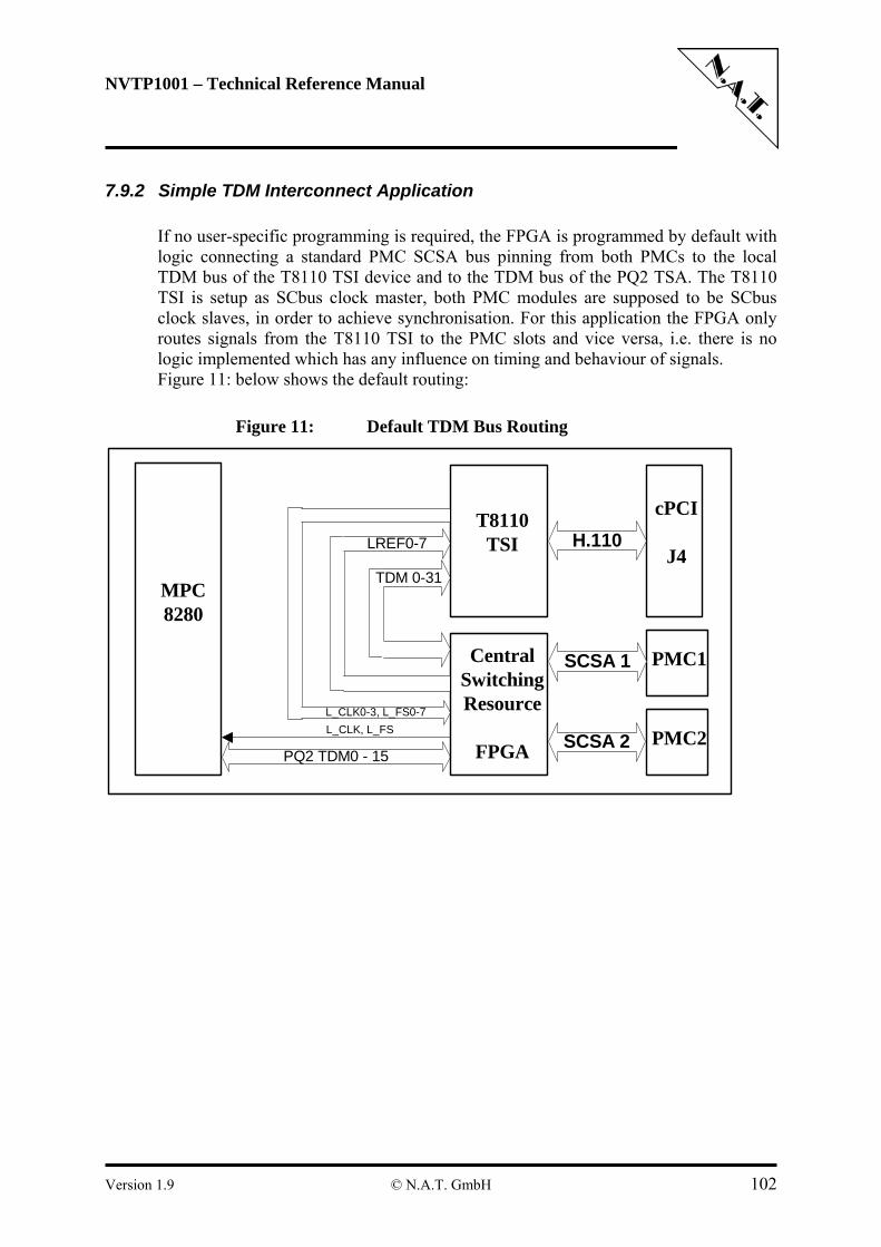
NVTP1001 – Technical Reference Manual
7.9.2 Simple TDM Interconnect Application If no user-specific programming is required, the FPGA is programmed by default with logic connecting a standard PMC SCSA bus pinning from both PMCs to the local TDM bus of the T8110 TSI device and to the TDM bus of the PQ2 TSA. The T8110 TSI is setup as SCbus clock master, both PMC modules are supposed to be SCbus clock slaves, in order to achieve synchronisation. For this application the FPGA only routes signals from the T8110 TSI to the PMC slots and vice versa, i.e. there is no logic implemented which has any influence on timing and behaviour of signals. Figure 11: below shows the default routing:
Figure 11: Default TDM Bus Routing
MPC8280
T8110TSI
PQ2 TDM0 - 15
CentralSwitchingResource
FPGA
LREF0-7
cPCI
J4H.110
TDM 0-31
L_CLK, L_FSL_CLK0-3, L_FS0-7
PMC1
PMC2
SCSA 1
SCSA 2
Version 1.9 © N.A.T. GmbH 102
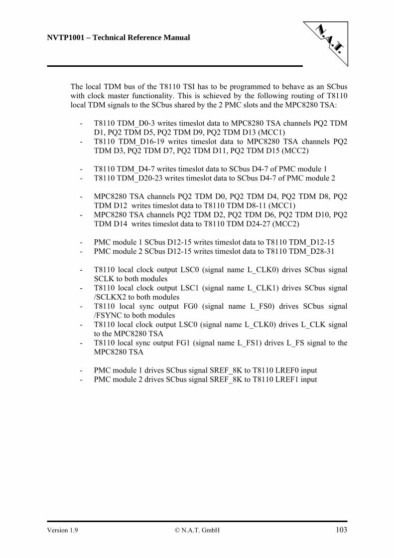
NVTP1001 – Technical Reference Manual
The local TDM bus of the T8110 TSI has to be programmed to behave as an SCbus with clock master functionality. This is schieved by the following routing of T8110 local TDM signals to the SCbus shared by the 2 PMC slots and the MPC8280 TSA:
- T8110 TDM_D0-3 writes timeslot data to MPC8280 TSA channels PQ2 TDM D1, PQ2 TDM D5, PQ2 TDM D9, PQ2 TDM D13 (MCC1)
- T8110 TDM_D16-19 writes timeslot data to MPC8280 TSA channels PQ2 TDM D3, PQ2 TDM D7, PQ2 TDM D11, PQ2 TDM D15 (MCC2)
- T8110 TDM_D4-7 writes timeslot data to SCbus D4-7 of PMC module 1 - T8110 TDM_D20-23 writes timeslot data to SCbus D4-7 of PMC module 2 - MPC8280 TSA channels PQ2 TDM D0, PQ2 TDM D4, PQ2 TDM D8, PQ2
TDM D12 writes timeslot data to T8110 TDM D8-11 (MCC1) - MPC8280 TSA channels PQ2 TDM D2, PQ2 TDM D6, PQ2 TDM D10, PQ2
TDM D14 writes timeslot data to T8110 TDM D24-27 (MCC2) - PMC module 1 SCbus D12-15 writes timeslot data to T8110 TDM_D12-15 - PMC module 2 SCbus D12-15 writes timeslot data to T8110 TDM_D28-31 - T8110 local clock output LSC0 (signal name L_CLK0) drives SCbus signal
SCLK to both modules - T8110 local clock output LSC1 (signal name L_CLK1) drives SCbus signal
/SCLKX2 to both modules - T8110 local sync output FG0 (signal name L_FS0) drives SCbus signal
/FSYNC to both modules - T8110 local clock output LSC0 (signal name L_CLK0) drives L_CLK signal
to the MPC8280 TSA - T8110 local sync output FG1 (signal name L_FS1) drives L_FS signal to the
MPC8280 TSA
- PMC module 1 drives SCbus signal SREF_8K to T8110 LREF0 input - PMC module 2 drives SCbus signal SREF_8K to T8110 LREF1 input
Version 1.9 © N.A.T. GmbH 103
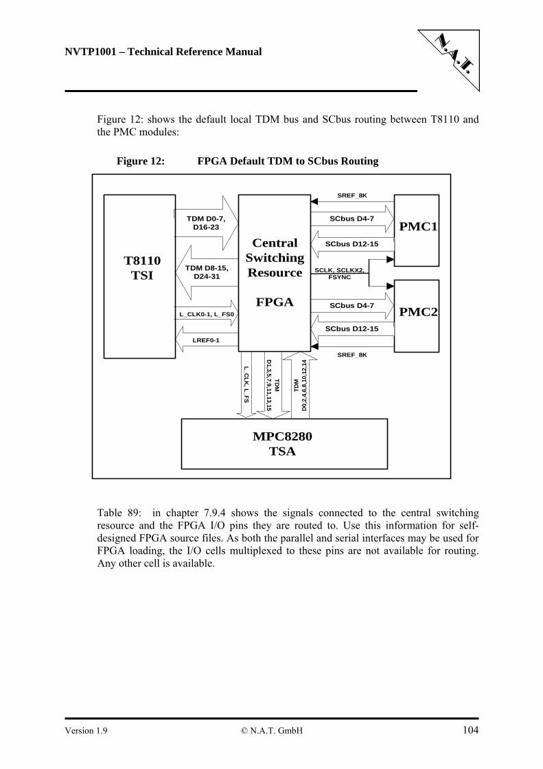
NVTP1001 – Technical Reference Manual
Figure 12: shows the default local TDM bus and SCbus routing between T8110 and the PMC modules:
Figure 12: FPGA Default TDM to SCbus Routing
SCbus D4-7
SREF_8K
PMC1
PMC2
SREF_8K
SCbus D12-15
SCbus D4-7
SCbus D12-15
SCLK, SCLKX2,FSYNC
TDM D0-7,D16-23
L_CLK0-1, L_FS0
LREF0-1
TDM D8-15,D24-31
T8110TSI
CentralSwitchingResource
FPGA
TDM
D1,3,5,7,9,11,13,15
L_CLK
, L_FS
MPC8280TSA
TDM
D0,
2,4,
6,8,
10,1
2,14
Table 89: in chapter 7.9.4 shows the signals connected to the central switching resource and the FPGA I/O pins they are routed to. Use this information for self-designed FPGA source files. As both the parallel and serial interfaces may be used for FPGA loading, the I/O cells multiplexed to these pins are not available for routing. Any other cell is available.
Version 1.9 © N.A.T. GmbH 104
NVTP1001 – Technical Reference Manual
7.9.3 Programmable TDM Interconnect Application If user-specific programming is required, the FPGA may be programmed by default with a more complex image, that allows programming of any signal routing combination between PMC1, PMC2, the local TDM bus of the T8110 TSI device and to the TDM busses of the PQ2 MCCs. For communication with the PMCs both SCbus protocol and H.110 bus protocol are supported. The T8110 TSI has to be setup as SCbus / H.110 clock master, both PMC modules are supposed to be SCbus / H.110 clock slaves, in order to achieve synchronisation. The only restriction when programming the direction of the TDM signals is, that they are grouped into groups of 4 lines. E.g. PMC module 1 SCbus D12-15 form one group, T8110 TDM_D4-7 form a 2nd, MPC8280 TSA channels PQ2 TDM D2, PQ2 TDM D6, PQ2 TDM D10, PQ2 TDM D14 (which refer to the TDM channels of MCC2) form a 3rd group, etc.. The direction of every group is programmable, as well as which other group it shall connect to. The selection of which local clock and frame sync of the TSI the interfaces (PMC1, PMC2, PQ2) shall synchronize to is also programmable. With the interfaces to the PMCs either SCbus control or H.110 control may be chosen, in case of H.110 the choice of primary or secondary set of clocks is also selectable by software. The setup of this TDM routing is done by 36 8-bit wide R/W-registers implemented within the FPGA, 26 for setting the data path, 6 setting the clock/sync structures, and 4 setting the LREF inputs for the T8110, which are accessible through the MPC8280 SPI interface. The following paragraphs describe these registers and there purpose in detail.
7.9.3.1 The FPGA SPI Interface Programming of the control registers implemented in the FPGA for setting up the routing paths is done by a SPI interface. The MPC8280 SPI interface on port pins PD16 – 19 is used for that purpose. Refer to chapter 39 of the MPC8280 User’s Manual for a description on how to program the SPI interface. The interface has to be setup in master mode, 16 bits character length. The first bit (MSB) is the R/W – bit, telleing the selected device whether the following access will be a read (MSB = “1”) or a write (MSB = “0”). the next 7 bits form the address, MSB first, LSB last. Then, the 8 data bits are read / written.
7.9.3.2 FPGA SPI Register Description The register area within the FPGA consists of 64 8-bit locations (6 address bits), 26 of which are used to define data paths (SPI addresses 0x0 – 0x19), 6 are used to set up clock/sync structures (SPI addresses 0x1a – 0x1f), 4 are used to set the LREF inputs (SPI addresses 0x20 – 0x23), 6 are used to set up IPMI port pin routing (SPI addresses 0x28 – 0x2d), 6 may be used as scratch registers (SPI addresses 0x24 – 0x27, 0x2e – 0x2f; R/W cells, they don’t serve any particular purpose), plus 1 status register which shows the FPGA revision code (SPI address 0x3f). Hence, 49 registers are defined, the remaining 15 locations are reserved for future use and cannot be written.
Version 1.9 © N.A.T. GmbH 105
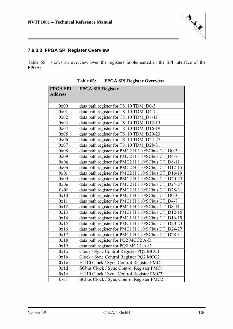
NVTP1001 – Technical Reference Manual
7.9.3.3 FPGA SPI Register Overview Table 65: shows an overview over the registers implemented in the SPI interface of the FPGA:
Table 65: FPGA SPI Register Overview
FPGA SPI Address
FPGA SPI Register
0x00 data path register for T8110 TDM_D0-3 0x01 data path register for T8110 TDM_D4-7 0x02 data path register for T8110 TDM_D8-11 0x03 data path register for T8110 TDM_D12-15 0x04 data path register for T8110 TDM_D16-19 0x05 data path register for T8110 TDM_D20-23 0x06 data path register for T8110 TDM_D24-27 0x07 data path register for T8110 TDM_D28-31 0x08 data path register for PMC2 H.110/SCbus CT_D0-3 0x09 data path register for PMC2 H.110/SCbus CT_D4-7 0x0a data path register for PMC2 H.110/SCbus CT_D8-11 0x0b data path register for PMC2 H.110/SCbus CT_D12-15 0x0c data path register for PMC2 H.110/SCbus CT_D16-19 0x0d data path register for PMC2 H.110/SCbus CT_D20-23 0x0e data path register for PMC2 H.110/SCbus CT_D24-27 0x0f data path register for PMC2 H.110/SCbus CT_D28-31 0x10 data path register for PMC1 H.110/SCbus CT_D0-3 0x11 data path register for PMC1 H.110/SCbus CT_D4-7 0x12 data path register for PMC1 H.110/SCbus CT_D8-11 0x13 data path register for PMC1 H.110/SCbus CT_D12-15 0x14 data path register for PMC1 H.110/SCbus CT_D16-19 0x15 data path register for PMC1 H.110/SCbus CT_D20-23 0x16 data path register for PMC1 H.110/SCbus CT_D24-27 0x17 data path register for PMC1 H.110/SCbus CT_D28-31 0x18 data path register for PQ2 MCC2 A-D 0x19 data path register for PQ2 MCC1 A-D 0x1a Clock / Sync Control Register PQ2 MCC1 0x1b Clock / Sync Control Register PQ2 MCC2 0x1c H.110 Clock / Sync Control Register PMC1 0x1d SCbus Clock / Sync Control Register PMC1 0x1e H.110 Clock / Sync Control Register PMC2 0x1f SCbus Clock / Sync Control Register PMC2
Version 1.9 © N.A.T. GmbH 106
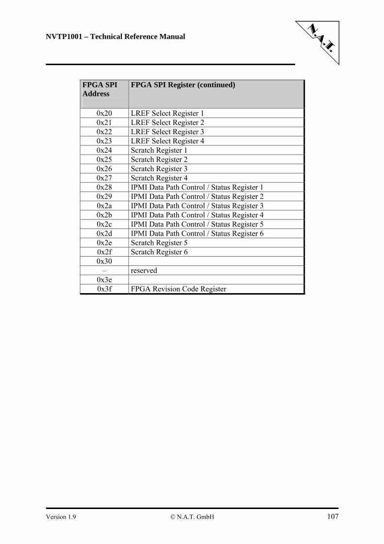
NVTP1001 – Technical Reference Manual
FPGA SPI Address
FPGA SPI Register (continued)
0x20 LREF Select Register 1 0x21 LREF Select Register 2 0x22 LREF Select Register 3 0x23 LREF Select Register 4 0x24 Scratch Register 1 0x25 Scratch Register 2 0x26 Scratch Register 3 0x27 Scratch Register 4 0x28 IPMI Data Path Control / Status Register 1 0x29 IPMI Data Path Control / Status Register 2 0x2a IPMI Data Path Control / Status Register 3 0x2b IPMI Data Path Control / Status Register 4 0x2c IPMI Data Path Control / Status Register 5 0x2d IPMI Data Path Control / Status Register 6 0x2e Scratch Register 5 0x2f Scratch Register 6 0x30
– reserved 0x3e 0x3f FPGA Revision Code Register
Version 1.9 © N.A.T. GmbH 107
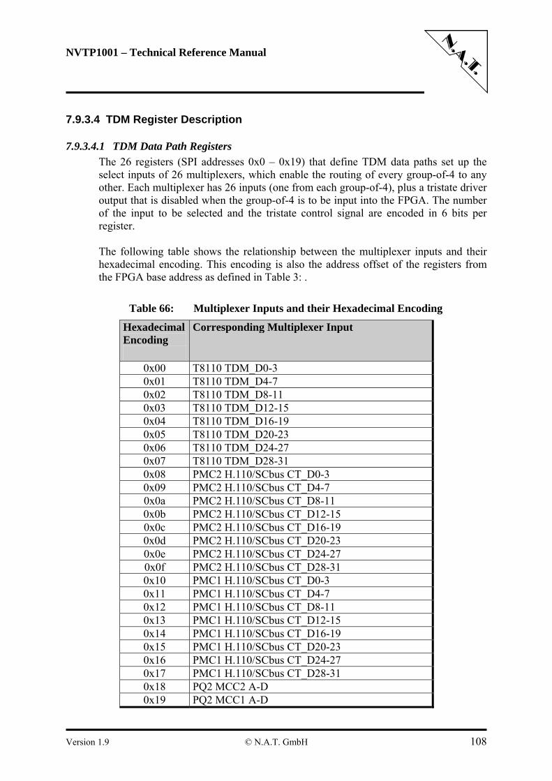
NVTP1001 – Technical Reference Manual
7.9.3.4 TDM Register Description
7.9.3.4.1 TDM Data Path Registers The 26 registers (SPI addresses 0x0 – 0x19) that define TDM data paths set up the select inputs of 26 multiplexers, which enable the routing of every group-of-4 to any other. Each multiplexer has 26 inputs (one from each group-of-4), plus a tristate driver output that is disabled when the group-of-4 is to be input into the FPGA. The number of the input to be selected and the tristate control signal are encoded in 6 bits per register. The following table shows the relationship between the multiplexer inputs and their hexadecimal encoding. This encoding is also the address offset of the registers from the FPGA base address as defined in Table 3: .
Table 66: Multiplexer Inputs and their Hexadecimal Encoding
Hexadecimal Encoding
Corresponding Multiplexer Input
0x00 T8110 TDM_D0-3 0x01 T8110 TDM_D4-7 0x02 T8110 TDM_D8-11 0x03 T8110 TDM_D12-15 0x04 T8110 TDM_D16-19 0x05 T8110 TDM_D20-23 0x06 T8110 TDM_D24-27 0x07 T8110 TDM_D28-31 0x08 PMC2 H.110/SCbus CT_D0-3 0x09 PMC2 H.110/SCbus CT_D4-7 0x0a PMC2 H.110/SCbus CT_D8-11 0x0b PMC2 H.110/SCbus CT_D12-15 0x0c PMC2 H.110/SCbus CT_D16-19 0x0d PMC2 H.110/SCbus CT_D20-23 0x0e PMC2 H.110/SCbus CT_D24-27 0x0f PMC2 H.110/SCbus CT_D28-31 0x10 PMC1 H.110/SCbus CT_D0-3 0x11 PMC1 H.110/SCbus CT_D4-7 0x12 PMC1 H.110/SCbus CT_D8-11 0x13 PMC1 H.110/SCbus CT_D12-15 0x14 PMC1 H.110/SCbus CT_D16-19 0x15 PMC1 H.110/SCbus CT_D20-23 0x16 PMC1 H.110/SCbus CT_D24-27 0x17 PMC1 H.110/SCbus CT_D28-31 0x18 PQ2 MCC2 A-D 0x19 PQ2 MCC1 A-D
Version 1.9 © N.A.T. GmbH 108
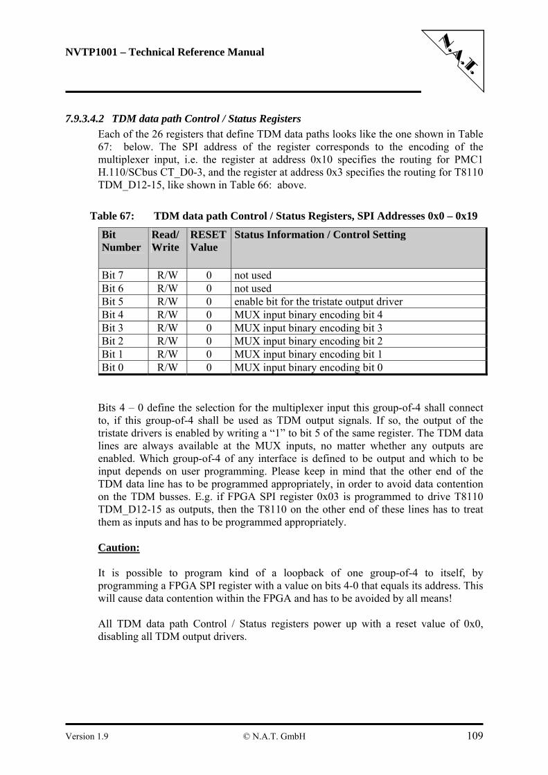
NVTP1001 – Technical Reference Manual
7.9.3.4.2 TDM data path Control / Status Registers Each of the 26 registers that define TDM data paths looks like the one shown in Table 67: below. The SPI address of the register corresponds to the encoding of the multiplexer input, i.e. the register at address 0x10 specifies the routing for PMC1 H.110/SCbus CT_D0-3, and the register at address 0x3 specifies the routing for T8110 TDM_D12-15, like shown in Table 66: above.
Table 67: TDM data path Control / Status Registers, SPI Addresses 0x0 – 0x19
Bit Number
Read/Write
RESET Value
Status Information / Control Setting
Bit 7 R/W 0 not used Bit 6 R/W 0 not used Bit 5 R/W 0 enable bit for the tristate output driver Bit 4 R/W 0 MUX input binary encoding bit 4 Bit 3 R/W 0 MUX input binary encoding bit 3 Bit 2 R/W 0 MUX input binary encoding bit 2 Bit 1 R/W 0 MUX input binary encoding bit 1 Bit 0 R/W 0 MUX input binary encoding bit 0
Bits 4 – 0 define the selection for the multiplexer input this group-of-4 shall connect to, if this group-of-4 shall be used as TDM output signals. If so, the output of the tristate drivers is enabled by writing a “1” to bit 5 of the same register. The TDM data lines are always available at the MUX inputs, no matter whether any outputs are enabled. Which group-of-4 of any interface is defined to be output and which to be input depends on user programming. Please keep in mind that the other end of the TDM data line has to be programmed appropriately, in order to avoid data contention on the TDM busses. E.g. if FPGA SPI register 0x03 is programmed to drive T8110 TDM_D12-15 as outputs, then the T8110 on the other end of these lines has to treat them as inputs and has to be programmed appropriately. Caution: It is possible to program kind of a loopback of one group-of-4 to itself, by programming a FPGA SPI register with a value on bits 4-0 that equals its address. This will cause data contention within the FPGA and has to be avoided by all means! All TDM data path Control / Status registers power up with a reset value of 0x0, disabling all TDM output drivers.
Version 1.9 © N.A.T. GmbH 109
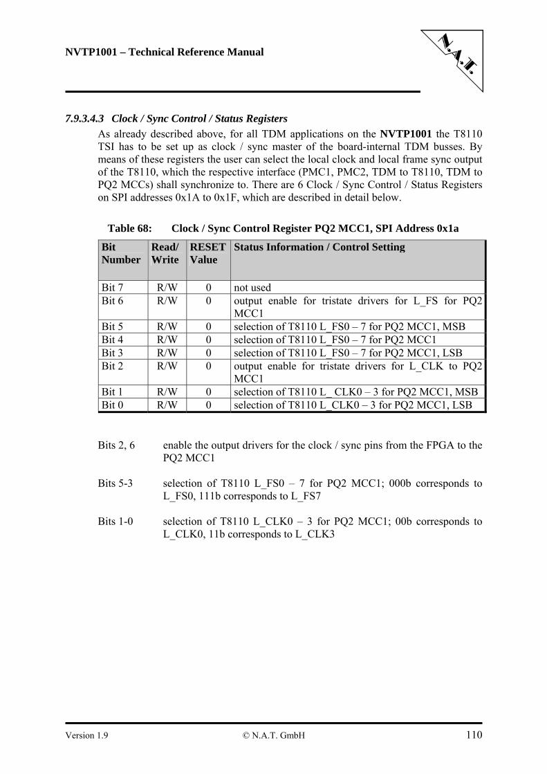
NVTP1001 – Technical Reference Manual
7.9.3.4.3 Clock / Sync Control / Status Registers As already described above, for all TDM applications on the NVTP1001 the T8110 TSI has to be set up as clock / sync master of the board-internal TDM busses. By means of these registers the user can select the local clock and local frame sync output of the T8110, which the respective interface (PMC1, PMC2, TDM to T8110, TDM to PQ2 MCCs) shall synchronize to. There are 6 Clock / Sync Control / Status Registers on SPI addresses 0x1A to 0x1F, which are described in detail below.
Table 68: Clock / Sync Control Register PQ2 MCC1, SPI Address 0x1a
Bit Number
Read/Write
RESET Value
Status Information / Control Setting
Bit 7 R/W 0 not used Bit 6 R/W 0 output enable for tristate drivers for L_FS for PQ2
MCC1 Bit 5 R/W 0 selection of T8110 L_FS0 – 7 for PQ2 MCC1, MSB Bit 4 R/W 0 selection of T8110 L_FS0 – 7 for PQ2 MCC1 Bit 3 R/W 0 selection of T8110 L_FS0 – 7 for PQ2 MCC1, LSB Bit 2 R/W 0 output enable for tristate drivers for L_CLK to PQ2
MCC1 Bit 1 R/W 0 selection of T8110 L_ CLK0 – 3 for PQ2 MCC1, MSB Bit 0 R/W 0 selection of T8110 L_CLK0 – 3 for PQ2 MCC1, LSB
Bits 2, 6 enable the output drivers for the clock / sync pins from the FPGA to the PQ2 MCC1
Bits 5-3 selection of T8110 L_FS0 – 7 for PQ2 MCC1; 000b corresponds to
L_FS0, 111b corresponds to L_FS7 Bits 1-0 selection of T8110 L_CLK0 – 3 for PQ2 MCC1; 00b corresponds to
L_CLK0, 11b corresponds to L_CLK3
Version 1.9 © N.A.T. GmbH 110
NVTP1001 – Technical Reference Manual
Table 69: Clock / Sync Control Register PQ2 MCC2, SPI Address 0x1b
Bit Number
Read/Write
RESET Value
Status Information / Control Setting
Bit 7 R/W 0 not used Bit 6 R/W 0 output enable for tristate drivers for L_FS for PQ2
MCC2 Bit 5 R/W 0 selection of T8110 L_FS0 – 7 for PQ2 MCC2, MSB Bit 4 R/W 0 selection of T8110 L_FS0 – 7 for PQ2 MCC2 Bit 3 R/W 0 selection of T8110 L_FS0 – 7 for PQ2 MCC2, LSB Bit 2 R/W 0 output enable for tristate drivers for L_CLK to PQ2
MCC2 Bit 1 R/W 0 selection of T8110 L_ CLK0 – 3 for PQ2 MCC2, MSB Bit 0 R/W 0 selection of T8110 L_ CLK0 – 3 for PQ2 MCC2, LSB
Bits 5-3 selection of T8110 L_FS0 – 7 for PQ2 MCC2; 000b corresponds to L_FS0, 111b corresponds to L_FS7
Bits 1-0 selection of T8110 L_CLK0 – 3 for PQ2 MCC2; 00b corresponds to
L_CLK0, 11b corresponds to L_CLK3 Bits 2, 6 enable the output drivers for the clock / sync pins from the FPGA to the
PQ2 MCC2
Version 1.9 © N.A.T. GmbH 111
NVTP1001 – Technical Reference Manual
Table 70: H.110 Clock / Sync Control Register PMC1, SPI Address 0x1c
Bit Number
Read/Write
RESET Value
Status Information / Control Setting
Bit 7 R/W 0 not used Bit 6 R/W 0 output enable for tristate drivers for PMC1 FRAME_B
and C8_B Bit 5 R/W 0 output enable for tristate drivers for PMC1 FRAME_A
and C8_A Bit 4 R/W 0 selection of T8110 L_CLK0 – 3 for PMC1 C8_A and
C8_B, MSB Bit 3 R/W 0 selection of T8110 L_CLK0 – 3 for PMC1 C8_A and
C8_B, LSB Bit 2 R/W 0 selection of T8110 L_FS0 – 7 for PMC1 FRAME_A
and FRAME_B, MSB Bit 1 R/W 0 selection of T8110 L_FS0 – 7 for PMC1 FRAME_A
and FRAME_B Bit 0 R/W 0 selection of T8110 L_FS0 – 7 for PMC1 FRAME_A
and FRAME_B, LSB
Table 71: SCbus Clock / Sync Control Register PMC1, SPI Address 0x1d
Bit Number
Read/Write
RESET Value
Status Information / Control Setting
Bit 7 R/W 0 output enable for tristate drivers for PMC1 SCbus clock/sync signals
Bit 6 R/W 0 selection of T8110 L_FS0 – 7 for PMC1 FSYNC, MSBBit 5 R/W 0 selection of T8110 L_FS0 – 7 for PMC1 FSYNC Bit 4 R/W 0 selection of T8110 L_FS0 – 7 for PMC1 FSYNC, LSB Bit 3 R/W 0 selection of T8110 L_CLK0 – 3 for PMC1 SCLKX2,
MSB Bit 2 R/W 0 selection of T8110 L_CLK0 – 3 for PMC1 SCLKX2,
LSB Bit 1 R/W 0 selection of T8110 L_CLK0 – 3 for PMC1 SCLK,
MSB Bit 0 R/W 0 selection of T8110 L_CLK0 – 3 for PMC1 SCLK, LSB
Version 1.9 © N.A.T. GmbH 112
NVTP1001 – Technical Reference Manual
Table 72: H.110 Clock / Sync Control Register PMC2, SPI Address 0x1e
Bit Number
Read/Write
RESET Value
Status Information / Control Setting
Bit 7 R/W 0 not used Bit 6 R/W 0 output enable for tristate drivers for PMC2 FRAME_B
and C8_B Bit 5 R/W 0 output enable for tristate drivers for PMC2 FRAME_A
and C8_A Bit 4 R/W 0 selection of T8110 L_CLK0 – 3 for PMC2 C8_A and
C8_B, MSB Bit 3 R/W 0 selection of T8110 L_CLK0 – 3 for PMC2 C8_A and
C8_B, LSB Bit 2 R/W 0 selection of T8110 L_FS0 – 7 for PMC2 FRAME_A
and FRAME_B, MSB Bit 1 R/W 0 selection of T8110 L_FS0 – 7 for PMC2 FRAME_A
and FRAME_B Bit 0 R/W 0 selection of T8110 L_FS0 – 7 for PMC2 FRAME_A
and FRAME_B, LSB
Table 73: SCbus Clock / Sync Control Register PMC2, SPI Address 0x1f
Bit Number
Read/Write
RESET Value
Status Information / Control Setting
Bit 7 R/W 0 output enable for tristate drivers for PMC2 SCbus clock/sync signals
Bit 6 R/W 0 selection of T8110 L_FS0 – 7 for PMC2 FSYNC, MSBBit 5 R/W 0 selection of T8110 L_FS0 – 7 for PMC2 FSYNC Bit 4 R/W 0 selection of T8110 L_FS0 – 7 for PMC2 FSYNC, LSB Bit 3 R/W 0 selection of T8110 L_CLK0 – 3 for PMC2 SCLKX2,
MSB Bit 2 R/W 0 selection of T8110 L_CLK0 – 3 for PMC2 SCLKX2,
LSB Bit 1 R/W 0 selection of T8110 L_CLK0 – 3 for PMC2 SCLK,
MSB Bit 0 R/W 0 selection of T8110 L_CLK0 – 3 for PMC2 SCLK, LSB
All clock / sync control / status registers power up with a reset value of 0x0, disabling all timing control signal output drivers.
Version 1.9 © N.A.T. GmbH 113
NVTP1001 – Technical Reference Manual
7.9.3.5 SYNC to LREF Routing There are up tp 3 SYNC signals coming from each PMC module, each of which can be used to be the timing master for the entire system including the H.110 backplane. Therefore, these 6 SYNC signals connect to the LREF inputs of the T8110 TSI device. In order to provide utmost flexibility, 4 registers were provided to allow the routing of any SYNC signal to any LREF input. These 4 LREF Select Registers occupy SPI addresses 0x20 to 0x23, and are described in detail below. There are additional 4 LREF Select Registers on SPI addresses 0x24 to 0x27, which are reserved for future use.
Table 74: LREF Select Register 1, SPI Address 0x20
Bit Number
Read/Write
RESET Value
Status Information / Control Setting
Bit 7 R/W 0 output enable for tristate driver for T8110 LREF1 signalBit 6 R/W 0 selection of T8110 LREF1 input, MSB Bit 5 R/W 0 selection of T8110 LREF1 input Bit 4 R/W 0 selection of T8110 LREF1 input, LSB Bit 3 R/W 0 output enable for tristate driver for T8110 LREF0 signalBit 2 R/W 0 selection of T8110 LREF0 input, MSB Bit 1 R/W 0 selection of T8110 LREF0 input Bit 0 R/W 0 selection of T8110 LREF0 input, LSB
Bits 2-0, 4-6 selection of T8110 Sync input for LREFx
Table 75: LREF Routing between PMC Sync Signals and T8110 TSI LREFs
SYNC Signal from PMC
Corresponding Bit Encoding, Bits 2-0, 4-6
SREF_8K from PMC 1 000b SREF_8K from PMC 2 001b NETRFEF1 from PMC 1 010b NETRFEF1 from PMC 2 011b NETRFEF2 from PMC 1 100b NETRFEF2 from PMC 2 101b none, driven high 110b none, driven high 111b
Bits 3, 7 enable output drivers for the LREF pins from the FPGA to the T8110
Version 1.9 © N.A.T. GmbH 114
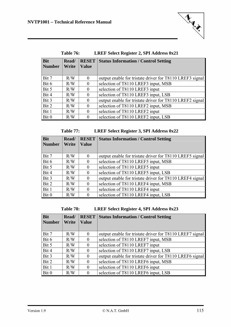
NVTP1001 – Technical Reference Manual
Table 76: LREF Select Register 2, SPI Address 0x21
Bit Number
Read/Write
RESET Value
Status Information / Control Setting
Bit 7 R/W 0 output enable for tristate driver for T8110 LREF3 signalBit 6 R/W 0 selection of T8110 LREF3 input, MSB Bit 5 R/W 0 selection of T8110 LREF3 input Bit 4 R/W 0 selection of T8110 LREF3 input, LSB Bit 3 R/W 0 output enable for tristate driver for T8110 LREF2 signalBit 2 R/W 0 selection of T8110 LREF2 input, MSB Bit 1 R/W 0 selection of T8110 LREF2 input Bit 0 R/W 0 selection of T8110 LREF2 input, LSB
Table 77: LREF Select Register 3, SPI Address 0x22
Bit Number
Read/Write
RESET Value
Status Information / Control Setting
Bit 7 R/W 0 output enable for tristate driver for T8110 LREF5 signalBit 6 R/W 0 selection of T8110 LREF5 input, MSB Bit 5 R/W 0 selection of T8110 LREF5 input Bit 4 R/W 0 selection of T8110 LREF5 input, LSB Bit 3 R/W 0 output enable for tristate driver for T8110 LREF4 signalBit 2 R/W 0 selection of T8110 LREF4 input, MSB Bit 1 R/W 0 selection of T8110 LREF4 input Bit 0 R/W 0 selection of T8110 LREF4 input, LSB
Table 78: LREF Select Register 4, SPI Address 0x23
Bit Number
Read/Write
RESET Value
Status Information / Control Setting
Bit 7 R/W 0 output enable for tristate driver for T8110 LREF7 signalBit 6 R/W 0 selection of T8110 LREF7 input, MSB Bit 5 R/W 0 selection of T8110 LREF7 input Bit 4 R/W 0 selection of T8110 LREF7 input, LSB Bit 3 R/W 0 output enable for tristate driver for T8110 LREF6 signalBit 2 R/W 0 selection of T8110 LREF6 input, MSB Bit 1 R/W 0 selection of T8110 LREF6 input Bit 0 R/W 0 selection of T8110 LREF6 input, LSB
Version 1.9 © N.A.T. GmbH 115
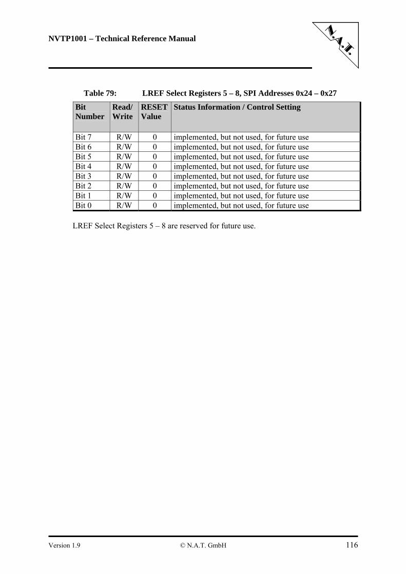
NVTP1001 – Technical Reference Manual
Table 79: LREF Select Registers 5 – 8, SPI Addresses 0x24 – 0x27
Bit Number
Read/Write
RESET Value
Status Information / Control Setting
Bit 7 R/W 0 implemented, but not used, for future use Bit 6 R/W 0 implemented, but not used, for future use Bit 5 R/W 0 implemented, but not used, for future use Bit 4 R/W 0 implemented, but not used, for future use Bit 3 R/W 0 implemented, but not used, for future use Bit 2 R/W 0 implemented, but not used, for future use Bit 1 R/W 0 implemented, but not used, for future use Bit 0 R/W 0 implemented, but not used, for future use
LREF Select Registers 5 – 8 are reserved for future use.
Version 1.9 © N.A.T. GmbH 116
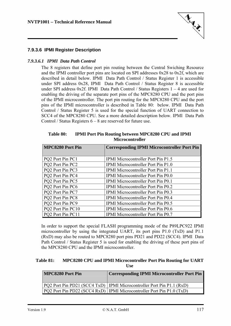
NVTP1001 – Technical Reference Manual
7.9.3.6 IPMI Register Description
7.9.3.6.1 IPMI Data Path Control The 8 registers that define port pin routing between the Central Swiching Resource and the IPMI controller port pins are located on SPI addresses 0x28 to 0x2f, which are described in detail below. IPMI Data Path Control / Status Register 1 is accessible under SPI address 0x28, IPMI Data Path Control / Status Register 8 is accessible under SPI address 0x2f. IPMI Data Path Control / Status Registers 1 – 4 are used for enabling the driving of the separate port pins of the MPC8280 CPU and the port pins of the IPMI microcontroller. The port pin routing for the MPC8280 CPU and the port pins of the IPMI microcontroller is described in Table 80: below. IPMI Data Path Control / Status Register 5 is used for the special function of UART connection to SCC4 of the MPC8280 CPU. See a more detailed description below. IPMI Data Path Control / Status Registers 6 – 8 are reserved for future use.
Table 80: IPMI Port Pin Routing between MPC8280 CPU and IPMI Microcontroller
MPC8280 Port Pin
Corresponding IPMI Microcontroller Port Pin
PQ2 Port Pin PC1 IPMI Microcontroller Port Pin P1.5 PQ2 Port Pin PC2 IPMI Microcontroller Port Pin P1.0 PQ2 Port Pin PC3 IPMI Microcontroller Port Pin P1.1 PQ2 Port Pin PC4 IPMI Microcontroller Port Pin P0.0 PQ2 Port Pin PC5 IPMI Microcontroller Port Pin P0.1 PQ2 Port Pin PC6 IPMI Microcontroller Port Pin P0.2 PQ2 Port Pin PC7 IPMI Microcontroller Port Pin P0.3 PQ2 Port Pin PC8 IPMI Microcontroller Port Pin P0.4 PQ2 Port Pin PC9 IPMI Microcontroller Port Pin P0.5 PQ2 Port Pin PC10 IPMI Microcontroller Port Pin P0.6 PQ2 Port Pin PC11 IPMI Microcontroller Port Pin P0.7
In order to support the special FLASH programming mode of the P89LPC922 IPMI microcontroller by using the integrated UART, its port pins P1.0 (TxD) and P1.1 (RxD) may also be routed to MPC8280 port pins PD21 and PD22 (SCC4). IPMI Data Path Control / Status Register 5 is used for enabling the driving of these port pins of the MPC8280 CPU and the IPMI microcontroller.
Table 81: MPC8280 CPU and IPMI Microcontroller Port Pin Routing for UART Use
MPC8280 Port Pin
Corresponding IPMI Microcontroller Port Pin
PQ2 Port Pin PD21 (SCC4 TxD) IPMI Microcontroller Port Pin P1.1 (RxD) PQ2 Port Pin PD22 (SCC4 RxD) IPMI Microcontroller Port Pin P1.0 (TxD)
Version 1.9 © N.A.T. GmbH 117
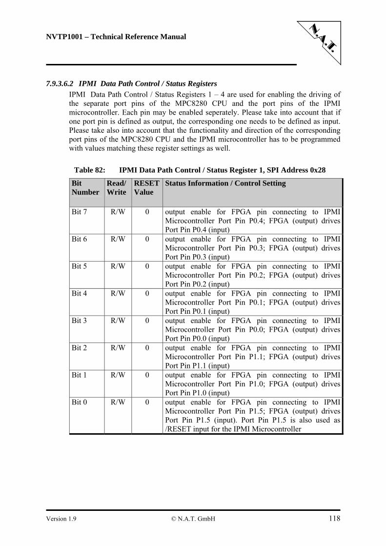
NVTP1001 – Technical Reference Manual
7.9.3.6.2 IPMI Data Path Control / Status Registers IPMI Data Path Control / Status Registers 1 – 4 are used for enabling the driving of the separate port pins of the MPC8280 CPU and the port pins of the IPMI microcontroller. Each pin may be enabled seperately. Please take into account that if one port pin is defined as output, the corresponding one needs to be defined as input. Please take also into account that the functionality and direction of the corresponding port pins of the MPC8280 CPU and the IPMI microcontroller has to be programmed with values matching these register settings as well.
Table 82: IPMI Data Path Control / Status Register 1, SPI Address 0x28
Bit Number
Read/Write
RESET Value
Status Information / Control Setting
Bit 7 R/W 0 output enable for FPGA pin connecting to IPMI Microcontroller Port Pin P0.4; FPGA (output) drives Port Pin P0.4 (input)
Bit 6 R/W 0 output enable for FPGA pin connecting to IPMI Microcontroller Port Pin P0.3; FPGA (output) drives Port Pin P0.3 (input)
Bit 5 R/W 0 output enable for FPGA pin connecting to IPMI Microcontroller Port Pin P0.2; FPGA (output) drives Port Pin P0.2 (input)
Bit 4 R/W 0 output enable for FPGA pin connecting to IPMI Microcontroller Port Pin P0.1; FPGA (output) drives Port Pin P0.1 (input)
Bit 3 R/W 0 output enable for FPGA pin connecting to IPMI Microcontroller Port Pin P0.0; FPGA (output) drives Port Pin P0.0 (input)
Bit 2 R/W 0 output enable for FPGA pin connecting to IPMI Microcontroller Port Pin P1.1; FPGA (output) drives Port Pin P1.1 (input)
Bit 1 R/W 0 output enable for FPGA pin connecting to IPMI Microcontroller Port Pin P1.0; FPGA (output) drives Port Pin P1.0 (input)
Bit 0 R/W 0 output enable for FPGA pin connecting to IPMI Microcontroller Port Pin P1.5; FPGA (output) drives Port Pin P1.5 (input). Port Pin P1.5 is also used as /RESET input for the IPMI Microcontroller
Version 1.9 © N.A.T. GmbH 118
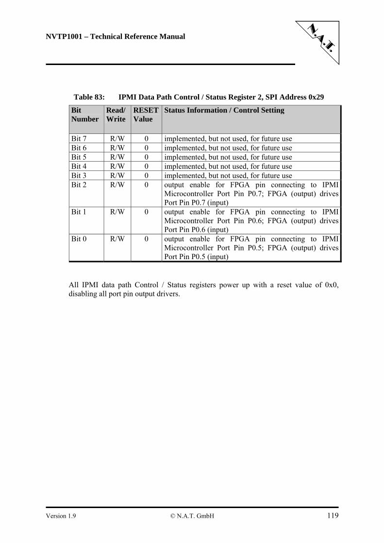
NVTP1001 – Technical Reference Manual
Table 83: IPMI Data Path Control / Status Register 2, SPI Address 0x29
Bit Number
Read/Write
RESET Value
Status Information / Control Setting
Bit 7 R/W 0 implemented, but not used, for future use Bit 6 R/W 0 implemented, but not used, for future use Bit 5 R/W 0 implemented, but not used, for future use Bit 4 R/W 0 implemented, but not used, for future use Bit 3 R/W 0 implemented, but not used, for future use Bit 2 R/W 0 output enable for FPGA pin connecting to IPMI
Microcontroller Port Pin P0.7; FPGA (output) drives Port Pin P0.7 (input)
Bit 1 R/W 0 output enable for FPGA pin connecting to IPMI Microcontroller Port Pin P0.6; FPGA (output) drives Port Pin P0.6 (input)
Bit 0 R/W 0 output enable for FPGA pin connecting to IPMI Microcontroller Port Pin P0.5; FPGA (output) drives Port Pin P0.5 (input)
All IPMI data path Control / Status registers power up with a reset value of 0x0, disabling all port pin output drivers.
Version 1.9 © N.A.T. GmbH 119
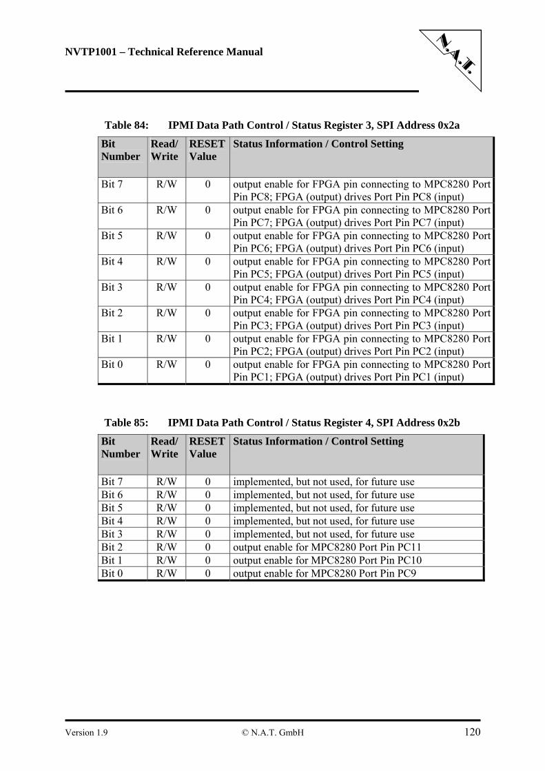
NVTP1001 – Technical Reference Manual
Table 84: IPMI Data Path Control / Status Register 3, SPI Address 0x2a
Bit Number
Read/Write
RESET Value
Status Information / Control Setting
Bit 7 R/W 0 output enable for FPGA pin connecting to MPC8280 Port Pin PC8; FPGA (output) drives Port Pin PC8 (input)
Bit 6 R/W 0 output enable for FPGA pin connecting to MPC8280 Port Pin PC7; FPGA (output) drives Port Pin PC7 (input)
Bit 5 R/W 0 output enable for FPGA pin connecting to MPC8280 Port Pin PC6; FPGA (output) drives Port Pin PC6 (input)
Bit 4 R/W 0 output enable for FPGA pin connecting to MPC8280 Port Pin PC5; FPGA (output) drives Port Pin PC5 (input)
Bit 3 R/W 0 output enable for FPGA pin connecting to MPC8280 Port Pin PC4; FPGA (output) drives Port Pin PC4 (input)
Bit 2 R/W 0 output enable for FPGA pin connecting to MPC8280 Port Pin PC3; FPGA (output) drives Port Pin PC3 (input)
Bit 1 R/W 0 output enable for FPGA pin connecting to MPC8280 Port Pin PC2; FPGA (output) drives Port Pin PC2 (input)
Bit 0 R/W 0 output enable for FPGA pin connecting to MPC8280 Port Pin PC1; FPGA (output) drives Port Pin PC1 (input)
Table 85: IPMI Data Path Control / Status Register 4, SPI Address 0x2b
Bit Number
Read/Write
RESET Value
Status Information / Control Setting
Bit 7 R/W 0 implemented, but not used, for future use Bit 6 R/W 0 implemented, but not used, for future use Bit 5 R/W 0 implemented, but not used, for future use Bit 4 R/W 0 implemented, but not used, for future use Bit 3 R/W 0 implemented, but not used, for future use Bit 2 R/W 0 output enable for MPC8280 Port Pin PC11 Bit 1 R/W 0 output enable for MPC8280 Port Pin PC10 Bit 0 R/W 0 output enable for MPC8280 Port Pin PC9
Version 1.9 © N.A.T. GmbH 120
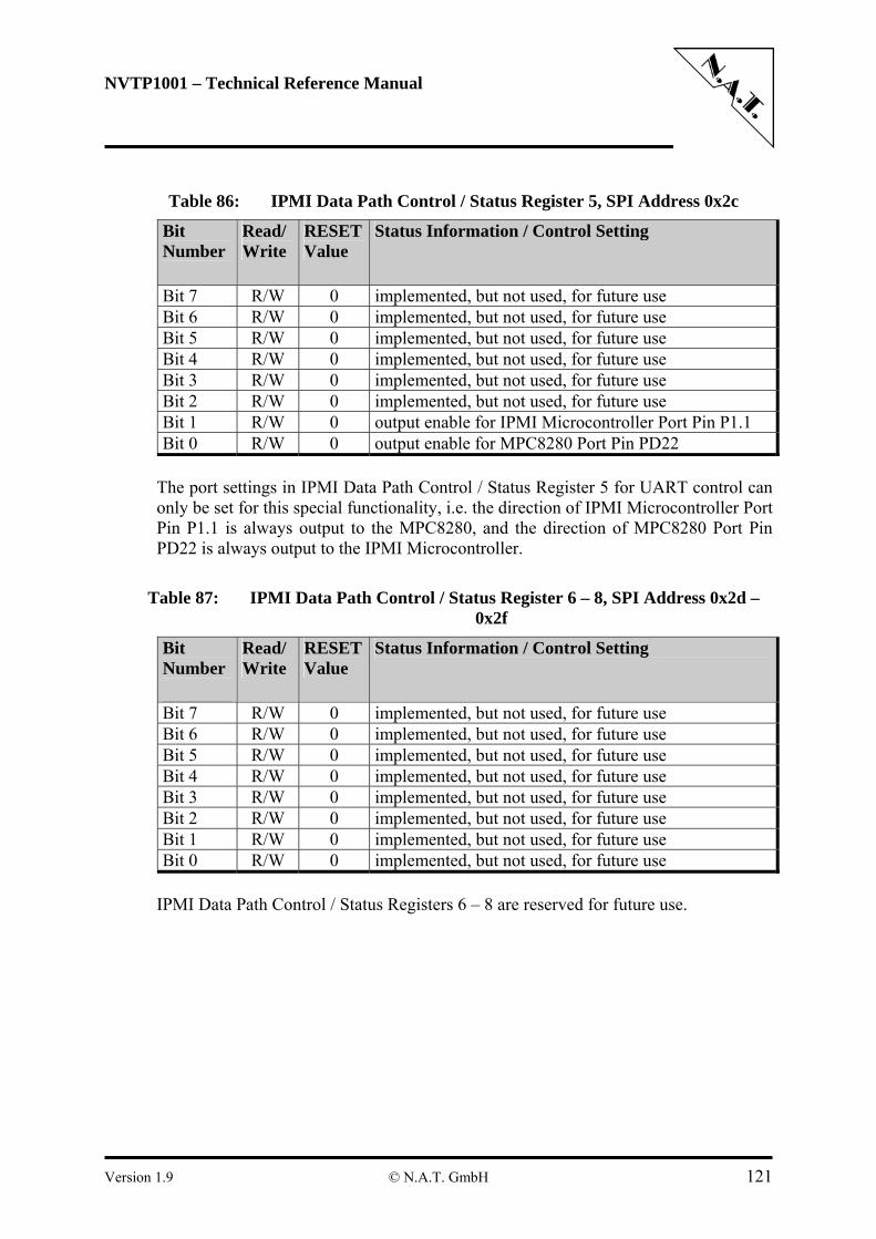
NVTP1001 – Technical Reference Manual
Table 86: IPMI Data Path Control / Status Register 5, SPI Address 0x2c
Bit Number
Read/Write
RESET Value
Status Information / Control Setting
Bit 7 R/W 0 implemented, but not used, for future use Bit 6 R/W 0 implemented, but not used, for future use Bit 5 R/W 0 implemented, but not used, for future use Bit 4 R/W 0 implemented, but not used, for future use Bit 3 R/W 0 implemented, but not used, for future use Bit 2 R/W 0 implemented, but not used, for future use Bit 1 R/W 0 output enable for IPMI Microcontroller Port Pin P1.1 Bit 0 R/W 0 output enable for MPC8280 Port Pin PD22
The port settings in IPMI Data Path Control / Status Register 5 for UART control can only be set for this special functionality, i.e. the direction of IPMI Microcontroller Port Pin P1.1 is always output to the MPC8280, and the direction of MPC8280 Port Pin PD22 is always output to the IPMI Microcontroller.
Table 87: IPMI Data Path Control / Status Register 6 – 8, SPI Address 0x2d – 0x2f
Bit Number
Read/Write
RESET Value
Status Information / Control Setting
Bit 7 R/W 0 implemented, but not used, for future use Bit 6 R/W 0 implemented, but not used, for future use Bit 5 R/W 0 implemented, but not used, for future use Bit 4 R/W 0 implemented, but not used, for future use Bit 3 R/W 0 implemented, but not used, for future use Bit 2 R/W 0 implemented, but not used, for future use Bit 1 R/W 0 implemented, but not used, for future use Bit 0 R/W 0 implemented, but not used, for future use
IPMI Data Path Control / Status Registers 6 – 8 are reserved for future use.
Version 1.9 © N.A.T. GmbH 121
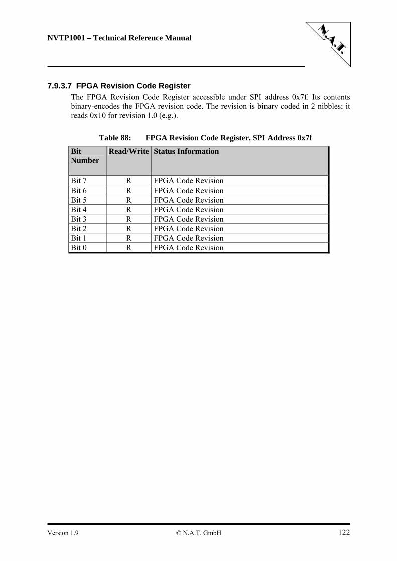
NVTP1001 – Technical Reference Manual
7.9.3.7 FPGA Revision Code Register The FPGA Revision Code Register accessible under SPI address 0x7f. Its contents binary-encodes the FPGA revision code. The revision is binary coded in 2 nibbles; it reads 0x10 for revision 1.0 (e.g.).
Table 88: FPGA Revision Code Register, SPI Address 0x7f
Bit Number
Read/Write Status Information
Bit 7 R FPGA Code Revision Bit 6 R FPGA Code Revision Bit 5 R FPGA Code Revision Bit 4 R FPGA Code Revision Bit 3 R FPGA Code Revision Bit 2 R FPGA Code Revision Bit 1 R FPGA Code Revision Bit 0 R FPGA Code Revision
Version 1.9 © N.A.T. GmbH 122
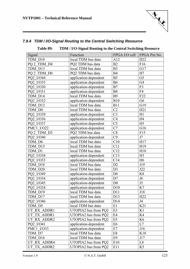
NVTP1001 – Technical Reference Manual
7.9.4 TDM / I/O-Signal Routing to the Central Switching Resource
Table 89: TDM / I/O-Signal Routing to the Central Switching Resource
Signal Function FPGA I/O cell FPGA Pin No.TDM_D10 local TDM bus data A12 D22 PQ 2_TDM_D4 PQ2 TDM bus data B2 F16 TDM_D13 local TDM bus data B3 G17 PQ 2_TDM_D0 PQ2 TDM bus data B4 H7 PQ2_I/O44 application-dependent B5 G5 PQ2_I/O35 application-dependent B6 G4 PQ2_I/O30 application-dependent B7 F3 PQ2_I/O31 application-dependent B8 F4 TDM_D14 local TDM bus data B9 F22 PQ2_I/O32 application-dependent B10 G6 TDM_D12 local TDM bus data B11 G19 TDM_D0 local TDM bus data C2 H21 PQ2_I/O39 application-dependent C3 H1 PQ2_I/O36 application-dependent C4 H4 PQ2_I/O37 application-dependent C5 H5 PMC1_I/O22 application-dependent C7 G16 PQ 2_TDM_D3 PQ2 TDM bus data C8 F15 PQ2_I/O40 application-dependent C9 J7 TDM_D6 local TDM bus data C10 H17 TDM_D15 local TDM bus data C11 H19 TDM_D1 local TDM bus data C12 H18 PQ2_I/O38 application-dependent C13 H3 PQ2_I/O33 application-dependent C14 H6 TDM_D18 local TDM bus data D2 J19 TDM_D20 local TDM bus data D3 J22 PQ2_I/O49 application-dependent D6 K8 PQ2_I/O34 application-dependent D7 J6 PQ2_I/O45 application-dependent D8 J5 PQ2_I/O24 application-dependent D10 K7 TDM_D19 local TDM bus data D11 J18 TDM_D17 local TDM bus data D13 H22 PQ2_I/O46 application-dependent D14 J4 TDM_D5 local TDM bus data E1 K21 UT_RX_ADDR1 UTOPIA2 bus from PQ2 E3 K1 UT_TX_ADDR1 UTOPIA2 bus from PQ2 E4 K4 UT_RX_ADDR2 UTOPIA2 bus from PQ2 E5 K6 PQ2_I/O41 application-dependent E6 L7 PMC1_I/O33 application-dependent E7 J16 TDM_D7 local TDM bus data E8 K18 TDM_D16 local TDM bus data E9 J17 UT_RX_ADDR4 UTOPIA2 bus from PQ2 E10 L8 UT_TX_ADDR2 UTOPIA2 bus from PQ2 E11 K5
Version 1.9 © N.A.T. GmbH 123
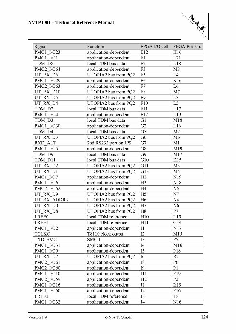
NVTP1001 – Technical Reference Manual
Signal Function FPGA I/O cell FPGA Pin No.PMC1_I/O23 application-dependent E12 H16 PMC1_I/O1 application-dependent F1 L21 TDM_D8 local TDM bus data F2 L18 PMC2_I/O64 application-dependent F3 M8 UT_RX_D6 UTOPIA2 bus from PQ2 F5 L4 PMC1_I/O29 application-dependent F6 K16 PMC2_I/O63 application-dependent F7 L6 UT_RX_D10 UTOPIA2 bus from PQ2 F8 M7 UT_RX_D5 UTOPIA2 bus from PQ2 F9 L3 UT_RX_D4 UTOPIA2 bus from PQ2 F10 L5 TDM_D2 local TDM bus data F11 L17 PMC1_I/O4 application-dependent F12 L19 TDM_D3 local TDM bus data G1 M18 PMC1_I/O30 application-dependent G2 L16 TDM_D4 local TDM bus data G5 M21 UT_RX_D3 UTOPIA2 bus from PQ2 G6 M6 RXD_ALT 2nd RS232 port on JP9 G7 M1 PMC1_I/O5 application-dependent G8 M19 TDM_D9 local TDM bus data G9 M17 TDM_D11 local TDM bus data G10 K15 UT_RX_D2 UTOPIA2 bus from PQ2 G11 M5 UT_RX_D1 UTOPIA2 bus from PQ2 G13 M4 PMC1_I/O7 application-dependent H2 N19 PMC1_I/O6 application-dependent H3 N18 PMC2_I/O62 application-dependent H4 N5 UT_RX_D9 UTOPIA2 bus from PQ2 H5 N7 UT_RX_ADDR3 UTOPIA2 bus from PQ2 H6 N4 UT_RX_D0 UTOPIA2 bus from PQ2 H7 N6 UT_RX_D8 UTOPIA2 bus from PQ2 H8 P7 LREF0 local TDM reference H10 L15 LREF1 local TDM reference H11 G14 PMC1_I/O2 application-dependent I1 N17 TCLKO T8110 clock output I2 M15 TXD_SMC SMC 1 I3 P5 PMC1_I/O31 application-dependent I4 M16 PMC1_I/O9 application-dependent I5 P18 UT_RX_D7 UTOPIA2 bus from PQ2 I6 R7 PMC2_I/O61 application-dependent I8 P6 PMC2_I/O60 application-dependent I9 P1 PMC1_I/O10 application-dependent I11 P19 PMC2_I/O59 application-dependent I12 P2 PMC1_I/O16 application-dependent J1 R19 PMC1_I/O60 application-dependent J2 P16 LREF2 local TDM reference J3 T8 PMC1_I/O32 application-dependent J4 N16
Version 1.9 © N.A.T. GmbH 124
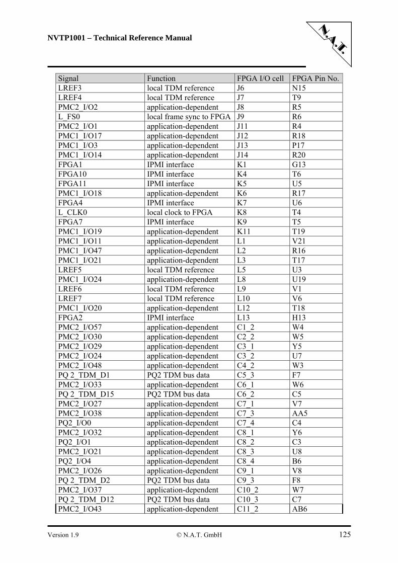
NVTP1001 – Technical Reference Manual
Signal Function FPGA I/O cell FPGA Pin No.LREF3 local TDM reference J6 N15 LREF4 local TDM reference J7 T9 PMC2_I/O2 application-dependent J8 R5 L_FS0 local frame sync to FPGA J9 R6 PMC2_I/O1 application-dependent J11 R4 PMC1_I/O17 application-dependent J12 R18 PMC1_I/O3 application-dependent J13 P17 PMC1_I/O14 application-dependent J14 R20 FPGA1 IPMI interface K1 G13 FPGA10 IPMI interface K4 T6 FPGA11 IPMI interface K5 U5 PMC1_I/O18 application-dependent K6 R17 FPGA4 IPMI interface K7 U6 L_CLK0 local clock to FPGA K8 T4 FPGA7 IPMI interface K9 T5 PMC1_I/O19 application-dependent K11 T19 PMC1_I/O11 application-dependent L1 V21 PMC1_I/O47 application-dependent L2 R16 PMC1_I/O21 application-dependent L3 T17 LREF5 local TDM reference L5 U3 PMC1_I/O24 application-dependent L8 U19 LREF6 local TDM reference L9 V1 LREF7 local TDM reference L10 V6 PMC1_I/O20 application-dependent L12 T18 FPGA2 IPMI interface L13 H13 PMC2_I/O57 application-dependent C1_2 W4 PMC2_I/O30 application-dependent C2_2 W5 PMC2_I/O29 application-dependent C3_1 Y5 PMC2_I/O24 application-dependent C3_2 U7 PMC2_I/O48 application-dependent C4_2 W3 PQ 2_TDM_D1 PQ2 TDM bus data C5_3 F7 PMC2_I/O33 application-dependent C6_1 W6 PQ 2_TDM_D15 PQ2 TDM bus data C6_2 C5 PMC2_I/O27 application-dependent C7_1 V7 PMC2_I/O38 application-dependent C7_3 AA5 PQ2_I/O0 application-dependent C7_4 C4 PMC2_I/O32 application-dependent C8_1 Y6 PQ2_I/O1 application-dependent C8_2 C3 PMC2_I/O21 application-dependent C8_3 U8 PQ2_I/O4 application-dependent C8_4 B6 PMC2_I/O26 application-dependent C9_1 V8 PQ 2_TDM_D2 PQ2 TDM bus data C9_3 F8 PMC2_I/O37 application-dependent C10_2 W7 PQ 2_TDM_D12 PQ2 TDM bus data C10_3 C7 PMC2_I/O43 application-dependent C11_2 AB6
Version 1.9 © N.A.T. GmbH 125
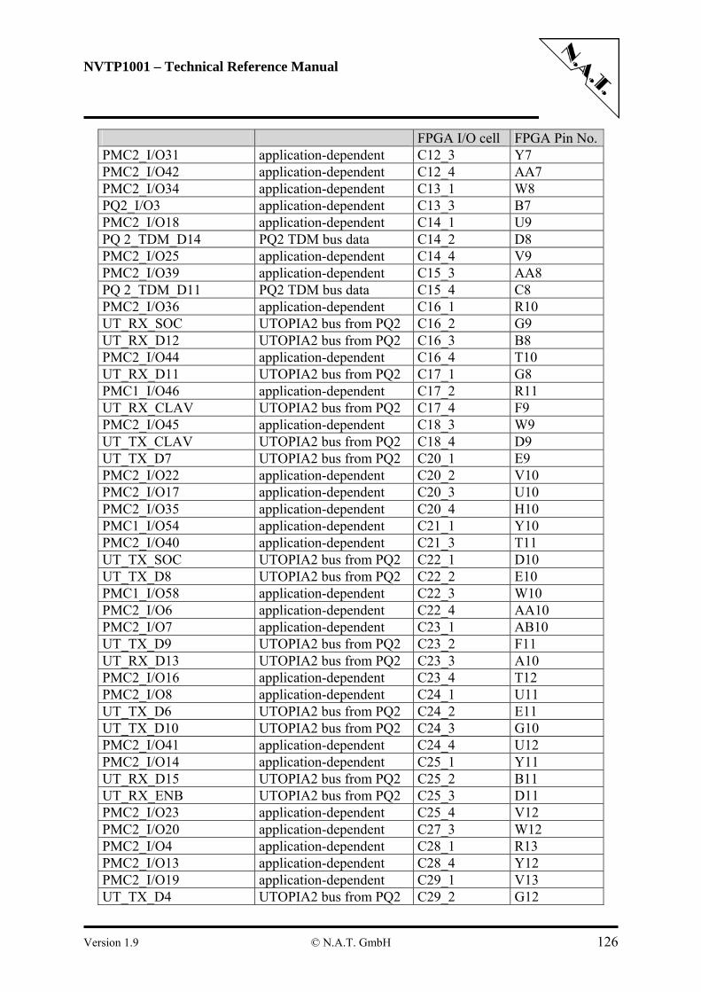
NVTP1001 – Technical Reference Manual
FPGA I/O cell FPGA Pin No.PMC2_I/O31 application-dependent C12_3 Y7 PMC2_I/O42 application-dependent C12_4 AA7 PMC2_I/O34 application-dependent C13_1 W8 PQ2_I/O3 application-dependent C13_3 B7 PMC2_I/O18 application-dependent C14_1 U9 PQ 2_TDM_D14 PQ2 TDM bus data C14_2 D8 PMC2_I/O25 application-dependent C14_4 V9 PMC2_I/O39 application-dependent C15_3 AA8 PQ 2_TDM_D11 PQ2 TDM bus data C15_4 C8 PMC2_I/O36 application-dependent C16_1 R10 UT_RX_SOC UTOPIA2 bus from PQ2 C16_2 G9 UT_RX_D12 UTOPIA2 bus from PQ2 C16_3 B8 PMC2_I/O44 application-dependent C16_4 T10 UT_RX_D11 UTOPIA2 bus from PQ2 C17_1 G8 PMC1_I/O46 application-dependent C17_2 R11 UT_RX_CLAV UTOPIA2 bus from PQ2 C17_4 F9 PMC2_I/O45 application-dependent C18_3 W9 UT_TX_CLAV UTOPIA2 bus from PQ2 C18_4 D9 UT_TX_D7 UTOPIA2 bus from PQ2 C20_1 E9 PMC2_I/O22 application-dependent C20_2 V10 PMC2_I/O17 application-dependent C20_3 U10 PMC2_I/O35 application-dependent C20_4 H10 PMC1_I/O54 application-dependent C21_1 Y10 PMC2_I/O40 application-dependent C21_3 T11 UT_TX_SOC UTOPIA2 bus from PQ2 C22_1 D10 UT_TX_D8 UTOPIA2 bus from PQ2 C22_2 E10 PMC1_I/O58 application-dependent C22_3 W10 PMC2_I/O6 application-dependent C22_4 AA10 PMC2_I/O7 application-dependent C23_1 AB10 UT_TX_D9 UTOPIA2 bus from PQ2 C23_2 F11 UT_RX_D13 UTOPIA2 bus from PQ2 C23_3 A10 PMC2_I/O16 application-dependent C23_4 T12 PMC2_I/O8 application-dependent C24_1 U11 UT_TX_D6 UTOPIA2 bus from PQ2 C24_2 E11 UT_TX_D10 UTOPIA2 bus from PQ2 C24_3 G10 PMC2_I/O41 application-dependent C24_4 U12 PMC2_I/O14 application-dependent C25_1 Y11 UT_RX_D15 UTOPIA2 bus from PQ2 C25_2 B11 UT_RX_ENB UTOPIA2 bus from PQ2 C25_3 D11 PMC2_I/O23 application-dependent C25_4 V12 PMC2_I/O20 application-dependent C27_3 W12 PMC2_I/O4 application-dependent C28_1 R13 PMC2_I/O13 application-dependent C28_4 Y12 PMC2_I/O19 application-dependent C29_1 V13 UT_TX_D4 UTOPIA2 bus from PQ2 C29_2 G12
Version 1.9 © N.A.T. GmbH 126
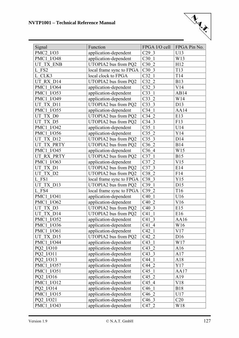
NVTP1001 – Technical Reference Manual
Signal Function FPGA I/O cell FPGA Pin No.PMC2_I/O3 application-dependent C29_3 U13 PMC1_I/O48 application-dependent C30_1 W13 UT_TX_ENB UTOPIA2 bus from PQ2 C30_2 H12 L_FS2 local frame sync to FPGA C30_3 T13 L_CLK3 local clock to FPGA C32_1 T14 UT_RX_D14 UTOPIA2 bus from PQ2 C32_2 B13 PMC1_I/O64 application-dependent C32_3 V14 PMC1_I/O53 application-dependent C33_1 AB14 PMC1_I/O49 application-dependent C33_2 W14 UT_TX_D11 UTOPIA2 bus from PQ2 C33_3 D13 PMC1_I/O55 application-dependent C34_1 AA14 UT_TX_D0 UTOPIA2 bus from PQ2 C34_2 E13 UT_TX_D5 UTOPIA2 bus from PQ2 C34_3 F13 PMC1_I/O42 application-dependent C35_1 U14 PMC1_I/O56 application-dependent C35_2 Y14 UT_TX_D12 UTOPIA2 bus from PQ2 C35_3 D14 UT_TX_PRTY UTOPIA2 bus from PQ2 C36_2 B14 PMC1_I/O45 application-dependent C36_4 W15 UT_RX_PRTY UTOPIA2 bus from PQ2 C37_1 B15 PMC1_I/O63 application-dependent C37_2 V15 UT_TX_D1 UTOPIA2 bus from PQ2 C37_3 E14 UT_TX_D2 UTOPIA2 bus from PQ2 C38_2 F14 L_FS1 local frame sync to FPGA C38_3 Y15 UT_TX_D13 UTOPIA2 bus from PQ2 C39_1 D15 L_FS4 local frame sync to FPGA C39_2 T16 PMC1_I/O41 application-dependent C40_1 U16 PMC1_I/O62 application-dependent C40_2 V16 UT_TX_D3 UTOPIA2 bus from PQ2 C40_3 E15 UT_TX_D14 UTOPIA2 bus from PQ2 C41_1 E16 PMC1_I/O52 application-dependent C41_3 AA16 PMC1_I/O36 application-dependent C41_4 W16 PMC1_I/O61 application-dependent C42_1 V17 UT_TX_D15 UTOPIA2 bus from PQ2 C42_2 D16 PMC1_I/O44 application-dependent C43_1 W17 PQ2_I/O10 application-dependent C43_2 A16 PQ2_I/O11 application-dependent C43_3 A17 PQ2_I/O13 application-dependent C44_1 A18 PMC1_I/O57 application-dependent C44_2 Y17 PMC1_I/O51 application-dependent C45_1 AA17 PQ2_I/O16 application-dependent C45_2 A19 PMC1_I/O12 application-dependent C45_4 V18 PQ2_I/O14 application-dependent C46_1 B18 PMC1_I/O15 application-dependent C46_2 U17 PQ2_I/O21 application-dependent C46_3 C20 PMC1_I/O43 application-dependent C47_2 W18
Version 1.9 © N.A.T. GmbH 127
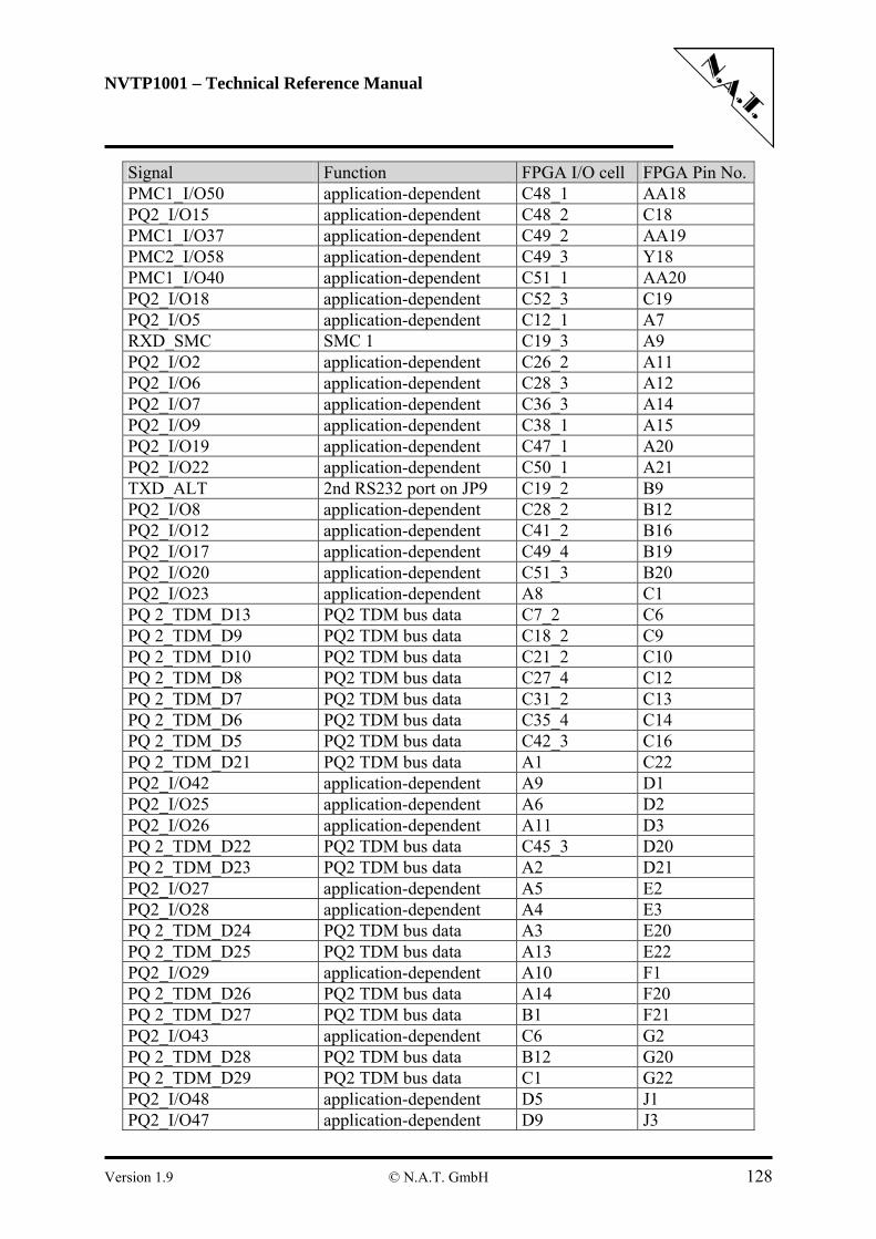
NVTP1001 – Technical Reference Manual
Signal Function FPGA I/O cell FPGA Pin No.PMC1_I/O50 application-dependent C48_1 AA18 PQ2_I/O15 application-dependent C48_2 C18 PMC1_I/O37 application-dependent C49_2 AA19 PMC2_I/O58 application-dependent C49_3 Y18 PMC1_I/O40 application-dependent C51_1 AA20 PQ2_I/O18 application-dependent C52_3 C19 PQ2_I/O5 application-dependent C12_1 A7 RXD_SMC SMC 1 C19_3 A9 PQ2_I/O2 application-dependent C26_2 A11 PQ2_I/O6 application-dependent C28_3 A12 PQ2_I/O7 application-dependent C36_3 A14 PQ2_I/O9 application-dependent C38_1 A15 PQ2_I/O19 application-dependent C47_1 A20 PQ2_I/O22 application-dependent C50_1 A21 TXD_ALT 2nd RS232 port on JP9 C19_2 B9 PQ2_I/O8 application-dependent C28_2 B12 PQ2_I/O12 application-dependent C41_2 B16 PQ2_I/O17 application-dependent C49_4 B19 PQ2_I/O20 application-dependent C51_3 B20 PQ2_I/O23 application-dependent A8 C1 PQ 2_TDM_D13 PQ2 TDM bus data C7_2 C6 PQ 2_TDM_D9 PQ2 TDM bus data C18_2 C9 PQ 2_TDM_D10 PQ2 TDM bus data C21_2 C10 PQ 2_TDM_D8 PQ2 TDM bus data C27_4 C12 PQ 2_TDM_D7 PQ2 TDM bus data C31_2 C13 PQ 2_TDM_D6 PQ2 TDM bus data C35_4 C14 PQ 2_TDM_D5 PQ2 TDM bus data C42_3 C16 PQ 2_TDM_D21 PQ2 TDM bus data A1 C22 PQ2_I/O42 application-dependent A9 D1 PQ2_I/O25 application-dependent A6 D2 PQ2_I/O26 application-dependent A11 D3 PQ 2_TDM_D22 PQ2 TDM bus data C45_3 D20 PQ 2_TDM_D23 PQ2 TDM bus data A2 D21 PQ2_I/O27 application-dependent A5 E2 PQ2_I/O28 application-dependent A4 E3 PQ 2_TDM_D24 PQ2 TDM bus data A3 E20 PQ 2_TDM_D25 PQ2 TDM bus data A13 E22 PQ2_I/O29 application-dependent A10 F1 PQ 2_TDM_D26 PQ2 TDM bus data A14 F20 PQ 2_TDM_D27 PQ2 TDM bus data B1 F21 PQ2_I/O43 application-dependent C6 G2 PQ 2_TDM_D28 PQ2 TDM bus data B12 G20 PQ 2_TDM_D29 PQ2 TDM bus data C1 G22 PQ2_I/O48 application-dependent D5 J1 PQ2_I/O47 application-dependent D9 J3
Version 1.9 © N.A.T. GmbH 128
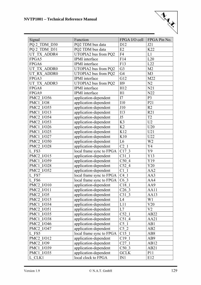
NVTP1001 – Technical Reference Manual
Signal Function FPGA I/O cell FPGA Pin No.PQ 2_TDM_D30 PQ2 TDM bus data D12 J21 PQ 2_TDM_D31 PQ2 TDM bus data E2 K22 UT_TX_ADDR4 UTOPIA2 bus from PQ2 F4 L1 FPGA5 IPMI interface F14 L20 FPGA6 IPMI interface F13 L22 UT_TX_ADDR0 UTOPIA2 bus from PQ2 G3 M2 UT_RX_ADDR0 UTOPIA2 bus from PQ2 G4 M3 FPGA3 IPMI interface G12 M22 UT_TX_ADDR3 UTOPIA2 bus from PQ2 H9 N2 FPGA8 IPMI interface H12 N21 FPGA9 IPMI interface H1 N22 PMC2_I/O56 application-dependent I7 P3 PMC1_I/O8 application-dependent I10 P21 PMC2_I/O55 application-dependent J10 R2 PMC1_I/O13 application-dependent I13 R21 PMC2_I/O54 application-dependent J5 T2 PMC2_I/O53 application-dependent K3 U2 PMC1_I/O26 application-dependent K2 U20 PMC1_I/O25 application-dependent K12 U21 PMC1_I/O27 application-dependent K10 U22 PMC2_I/O50 application-dependent L6 W2 PMC2_I/O28 application-dependent C2_1 Y4 L_FS3 local frame sync to FPGA C17_3 Y9 PMC2_I/O15 application-dependent C31_1 Y13 PMC1_I/O59 application-dependent C50_4 Y19 PMC1_I/O28 application-dependent C52_4 Y20 PMC2_I/O52 application-dependent C1_1 AA2 L_FS7 local frame sync to FPGA C4_1 AA3 L_FS6 local frame sync to FPGA C6_3 AA4 PMC2_I/O10 application-dependent C18_1 AA9 PMC2_I/O11 application-dependent C26_3 AA11 PMC2_I/O5 application-dependent C31_3 AA13 PMC2_I/O15 application-dependent L4 W1 PMC1_I/O34 application-dependent L11 V20 PMC2_I/O51 application-dependent L7 V2 PMC1_I/O35 application-dependent C52_1 AB22 PMC1_I/O38 application-dependent C51_4 AA21 PMC2_I/O46 application-dependent C5_1 AB1 PMC2_I/O47 application-dependent C5_2 AB2 L_FS5 local frame sync to FPGA C15_1 AB8 PMC2_I/O12 application-dependent C19_1 AB9 PMC2_I/O9 application-dependent C27_1 AB12 PMC1_I/O39 application-dependent C50_3 AB21 PMC1_I/O35 application-dependent GCLK P11 L_CLK1 local clock to FPGA IN1 E12
Version 1.9 © N.A.T. GmbH 129
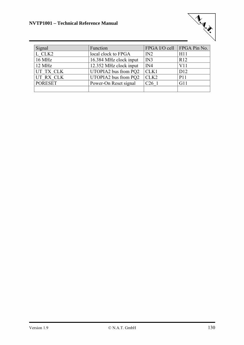
NVTP1001 – Technical Reference Manual
Signal Function FPGA I/O cell FPGA Pin No.L_CLK2 local clock to FPGA IN2 H11 16 MHz 16.384 MHz clock input IN3 R12 12 MHz 12.352 MHz clock input IN4 V11 UT_TX_CLK UTOPIA2 bus from PQ2 CLK1 D12 UT_RX_CLK UTOPIA2 bus from PQ2 CLK2 P11 PORESET Power-On Reset signal C26_1 G11
Version 1.9 © N.A.T. GmbH 130

NVTP1001 – Technical Reference Manual
8 Known Bugs and Restrictions
- use only PLL settings for the MPC8280 that result in a 66 MHz PCI clock
Version 1.9 © N.A.T. GmbH 131
NVTP1001 – Technical Reference Manual
Appendix A: Reference Documentation [1] PLX, PCI 6150 (HB4) PCI to PCI Bridge Data Book, May 2003, Version 2.0 [2] Motorola Inc., MPC8280 PowerQUICC II Family Reference Manual, 3/2004, Rev. 0 [3] Motorola Inc., MPC8280 PowerQUICC II Family Hardware Specifications,
Rev. 1.0, 2/2004 [4] Intel Corp., 21555 Non-Transparent PCI-to-PCI Bridge User Manual, July 2001 [5] Intel Corp., 82545 Gigabit Ethernet Controller Developers’s Manual, February 2002 [6] Agere Systems, Ambassador T8110 PCI-based H.100/H.110 Switch and Packet
Payload Engine, April 2001 [7] Infineon, V23818-K305-L17/L57 Data Sheet, January 2001 [8] AMD, AM79C973/AM79C975 Data Sheet, Rev. D, Amendment 0, February 1999 [9] Altera, ACEX 1K Programmable Logic Device Family, Data Sheet, Ver. 3.0, May
2001 [10] P89LPC920/921/922 User’s Manual, December 2003 [11] P89LPC920/921/922 Product Data, Rev. 06, November 2003
Version 1.9 © N.A.T. GmbH 132
NVTP1001 – Technical Reference Manual
Appendix B: Document’s History Revision Date Description Author
1.0 07.07.2004 initial version ga 1.1 14.12.2004 FPGA application sections added, RESET description
extended ga
1.2 15.02.2005 Reset strategy reworked ga 1.3 17.02.2005 adapted to PCB V1.1, IPMI added ga 1.4 30.05.2005 SW Reset to cPCI added ga 1.5 08.08.2005 amendment on page 100 ga 1.6 10.02.2006 ‘Statement on Environmental Protection’ added ga 1.7 11.04.2006 adapted to PCB V1.2, SPI Interface description of
Central Switching Resource corrected, CPLD Version Registers introduced
ga
1.8 12.07.2006 SPI Interface description of Central Switching Resource adapted
ga
1.9. 06.06.2007 chapters 2.3.3 and 2.3.4 added ga
Version 1.9 © N.A.T. GmbH 133