Embed Size (px)
Citation preview
Manual 3/16/2017
PSFNP7xxxxWxxx_PM963 Viking Technology
Revision A Page 1 of 52
www.vikingtechnology.com
NVMe PCIe SSD
M.2 Manual
NVMe PCIe SSD is a non-volatile, solid-state storage device delivering uncompromising performance, reliability and ruggedness for environmentally challenging applications.
Manual 3/16/2017
PSFNP7xxxxWxxx_PM963 Viking Technology
Revision A Page 2 of 52
www.vikingtechnology.com
Revision History Date Revision Description Checked By
3/16/17 A Initial Release based on PSFNP7xxxxWxxx and update PN table. Add VSFNP7480GWCHVSM
Manual 3/16/2017
PSFNP7xxxxWxxx_PM963 Viking Technology
Revision A Page 3 of 52
www.vikingtechnology.com
Legal Information Legal Information
Copyright© 2017 Sanmina Corporation. All rights reserved. The information in this document is proprietary and confidential to Sanmina Corporation. No part of this document may be reproduced in any form or by any means or used to make any derivative work (such as translation, transformation, or adaptation) without written permission from Sanmina. Sanmina reserves the right to revise this documentation and to make changes in content from time to time without obligation on the part of Sanmina to provide notification of such revision or change. Sanmina provides this documentation without warranty, term or condition of any kind, either expressed or implied, including, but not limited to, expressed and implied warranties of merchantability, fitness for a particular purpose, and non-infringement. While the information contained herein is believed to be accurate, such information is preliminary, and should not be relied upon for accuracy or completeness, and no representations or warranties of accuracy or completeness are made. In no event will Sanmina be liable for damages arising directly or indirectly from any use of or reliance upon the information contained in this document. Sanmina may make improvements or changes in the product(s) and/or the program(s) described in this documentation at any time. Sanmina, Viking Technology, Viking Modular Solutions, and Element logo are trademarks of Sanmina Corporation. Other company, product or service names mentioned herein may be trademarks or service marks of their respective owners.
Manual 3/16/2017
PSFNP7xxxxWxxx_PM963 Viking Technology
Revision A Page 4 of 52
www.vikingtechnology.com
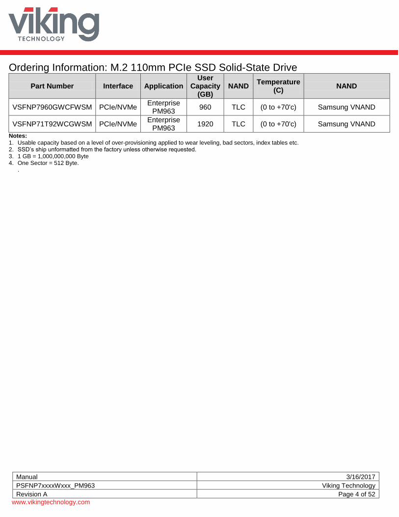
Ordering Information: M.2 110mm PCIe SSD Solid-State Drive
Part Number Interface Application User
Capacity (GB)
NAND Temperature
(C) NAND
VSFNP7960GWCFWSM PCIe/NVMe Enterprise
PM963 960 TLC (0 to +70'c) Samsung VNAND
VSFNP71T92WCGWSM PCIe/NVMe Enterprise
PM963 1920 TLC (0 to +70'c) Samsung VNAND
Notes:
1. Usable capacity based on a level of over-provisioning applied to wear leveling, bad sectors, index tables etc. 2. SSD’s ship unformatted from the factory unless otherwise requested. 3. 1 GB = 1,000,000,000 Byte 4. One Sector = 512 Byte.
.
Manual 3/16/2017
PSFNP7xxxxWxxx_PM963 Viking Technology
Revision A Page 5 of 52
www.vikingtechnology.com
Table of Contents
1 INTRODUCTION 10
1.1 Features 10
1.2 PCIE Interface 10
2 PRODUCT SPECIFICATIONS 11
2.1 Capacity and LBA count 11
2.2 Performance 11
2.3 Timing / Latency 12
2.4 Quality of Service (QoS) 12
2.5 Electrical Characteristics 12 2.5.1 Absolute Maximum Ratings 12 2.5.2 Supply Voltage 13 2.5.3 Power Consumption 13
2.6 Environmental Conditions 14 2.6.1 Temperature and Altitude 14 2.6.2 Shock and Vibration 14 2.6.3 Electromagnetic Immunity 14
2.7 Reliability 15
2.8 Data Security 15 2.8.1 Power Loss Protection 15 2.8.2 Sudden Power Off and Recovery 15
3 MECHANICAL INFORMATION 17
3.1 Dimensions 17
3.2 Card Edge Detail 18
Manual 3/16/2017
PSFNP7xxxxWxxx_PM963 Viking Technology
Revision A Page 6 of 52
www.vikingtechnology.com
3.3 M.2 SSD Weight 20
4 PIN AND SIGNAL DESCRIPTIONS 21
4.1 Signal and Power Description Tables 21
5 PCIE AND NVM EXPRESS REGISTERS 22
5.1 PCI Express Registers 22 5.1.1 PCI Register Summary 22 5.1.2 PCI Header Registers 22 5.1.3 PCI Power Management Registers 27 5.1.4 Message Signaled Interrupt Registers 28 5.1.5 MSI-X Registers 29 5.1.6 PCI Express Capability Registers 30 5.1.7 Advanced Error Reporting Registers 34 5.1.8 Device Serial Number Capability Register 39 5.1.9 Power Budgeting Extended Capability 39 5.1.10 Latency Tolerance Reporting Capability Registers 39 5.1.11 L1 Substates Capability Registers 40
5.2 NVM Express Registers 41 5.2.1 Register Summary 41 5.2.2 Controller Registers 42
6 SUPPORTED COMMAND SET 45
6.1 Admin Command Set 45 6.1.1 Identify Command 46
6.2 NVM Express I/O Command Set 50
6.3 SMART/Health Information 51
7 PRODUCT COMPLIANCE 52
8 REFERENCES 52
Manual 3/16/2017
PSFNP7xxxxWxxx_PM963 Viking Technology
Revision A Page 7 of 52
www.vikingtechnology.com
Table of Tables Table 2-1: Maximum Random Read / Write Input/Output Operations per Second (IOPS) _ 12 Table 2-2: Timing Specifications _________________________________________________ 12 Table 2-3: Absolute Maximum Ratings ____________________________________________ 13 Table 2-4: Operating Voltage ____________________________________________________ 13 Table 2-5: Power Consumption __________________________________________________ 13 Table 2-6: Temperature and Altitude Related Specifications ____________________________ 14 Table 2-7: Shock and Vibration Specifications _______________________________________ 14 Table 2-8: Reliability Specifications _______________________________________________ 15 Table 3-1: M.2 SSD weight ______________________________________________________ 20 Table 4-1: M.2 PCIE Connector Pinouts ___________________________________________ 21 Table 5-1: PCI Register Summary ________________________________________________ 22 Table 5-2: PCI Header Register Summary __________________________________________ 22 Table 5-3: Identifier Register ____________________________________________________ 23 Table 5-4: Command Register ___________________________________________________ 24 Table 5-5: Device Status Register ________________________________________________ 24 Table 5-6: Revision ID Register __________________________________________________ 24 Table 5-7: Class Code Register __________________________________________________ 24 Table 5-8: Cache Line Size Register ______________________________________________ 25 Table 5-9: Master Latency Timer Register __________________________________________ 25 Table 5-10: Header Type Register ________________________________________________ 25 Table 5-11: Built-in Self Test Register _____________________________________________ 25 Table 5-12: Memory Register Base Address Lower 32-bits (BAR0) Register _______________ 25 Table 5-13: Memory Register Base Address Upper 32-bits (BAR1) Register _______________ 25 Table 5-14: Index/Data Pair Register Base Address (BAR2) Register ____________________ 25 Table 5-15: BAR3 Register ______________________________________________________ 25 Table 5-16: Vendor Specific BAR4 Register ________________________________________ 26 Table 5-17: Vendor Specific BAR5 Register ________________________________________ 26 Table 5-18: Subsystem Identifier Register __________________________________________ 26 Table 5-19: Expansion ROM Register _____________________________________________ 26 Table 5-20: Capabilities Pointer Register ___________________________________________ 26 Table 5-21: Interrupt Information Register __________________________________________ 26 Table 5-22: Minimum Grant Register ______________________________________________ 26 Table 5-23: Maximum Latency Register ____________________________________________ 26 Table 5-24: PCI Power Management Capability Register Summary ______________________ 27 Table 5-25: PCI Power Management Capability ID Register ____________________________ 27 Table 5-26: PCI Power Management Capability Register ______________________________ 27 Table 5-27: PCI Power Management Control and Status Register _______________________ 27 Table 5-28: Message Signaled Interrupt Capability Register Summary ___________________ 28 Table 5-29: Message Signaled Interrupt Capability ID Register _________________________ 28 Table 5-30: Message Signaled Interrupt Control Register ______________________________ 28 Table 5-31: Message Signaled Interrupt Lower Address Register ________________________ 28 Table 5-32: Message Signaled Interrupt Upper Address Register ________________________ 28 Table 5-33: Message Signaled Interrupt Message Data Register ________________________ 28 Table 5-34: Message Signaled Interrupt Masked Bits Register __________________________ 28 Table 5-35: Message Signaled Interrupt Pending Bits Register _________________________ 29 Table 5-36: MSI-X Capability Register Summary _____________________________________ 29 Table 5-37: MSI-X Identifier Register ______________________________________________ 29 Table 5-38: MSI-X Control Register _______________________________________________ 29 Table 5-39: MSI-X Table Offset Register ___________________________________________ 29 Table 5-40: MSI-X Pending Bit Array Offset Register _________________________________ 29
Manual 3/16/2017
PSFNP7xxxxWxxx_PM963 Viking Technology
Revision A Page 8 of 52
www.vikingtechnology.com
Table 5-41: PCI Express Capability Register Summary________________________________ 30 Table 5-42: PCI Express Capability ID Register _____________________________________ 30 Table 5-43: PCI Express Capabilities Register ______________________________________ 30 Table 5-44: PCI Express Device Capabilities Register ________________________________ 30 Table 5-45: PCI Express Device Control Register ____________________________________ 31 Table 5-46: PCI Express Device Status Register _____________________________________ 31 Table 5-47: PCI Express Device Link Capabilities Register ____________________________ 31 Table 5-48: PCI Express Device Link Control Register ________________________________ 32 Table 5-49: PCI Express Device Link Status Register _________________________________ 32 Table 5-50: PCI Express Device Capabilities 2 Register _______________________________ 32 Table 5-51: PCI Express Device Control 2 Register __________________________________ 33 Table 5-52: PCI Express Device Status 2 Register ___________________________________ 33 Table 5-53: PCI Express Link Capabilities 2 Register _________________________________ 33 Table 5-54: PCI Express Link Control 2 Register _____________________________________ 33 Table 5-55: PCI Express Link Status 2 Register _____________________________________ 33 Table 5-56: Advanced Error Reporting Capability Register Summary _____________________ 34 Table 5-57: AER Capability ID Register ____________________________________________ 34 Table 5-58: AER Uncorrectable Error Status Register _________________________________ 34 Table 5-59: AER Uncorrectable Error Mask Register _________________________________ 35 Table 5-60: AER Uncorrectable Error Severity Register _______________________________ 35 Table 5-61: AER Correctable Error Status Register ___________________________________ 36 Table 5-62: AER Correctable Error Mask Register ___________________________________ 36 Table 5-63: AER Capabilities and Control Register ___________________________________ 36 Table 5-64: AER Header Log Register _____________________________________________ 37 Table 5-65: AER TLP Prefix Log Register __________________________________________ 37 Table 5-66: Secondary PCI Express Capability Register Summary ______________________ 37 Table 5-67: Secondary PCI Express Capability ID Register ____________________________ 37 Table 5-68: PCI Express Link Control 3 Register ____________________________________ 38 Table 5-69: PCI Express Lane Error Status Register __________________________________ 38 Table 5-70: PCI Express Lane 0 Equalization Register ________________________________ 38 Table 5-71: PCI Express Lane 1 Equalization Register _______________________________ 38 Table 5-72: PCI Express Lane 2 Equalization Register ________________________________ 38 Table 5-73: PCI Express Lane 3 Equalization Register ________________________________ 38 Table 5-74: Device Serial Number Capability Register Header _________________________ 39 Table 5-75: Serial Number Register Header (offset 0x4/0x8) ___________________________ 39 Table 5-76: Power Budgeting Extended Capability Header _____________________________ 39 Table 5-77: Data Register ______________________________________________________ 39 Table 5-78: Power Budget Capability Register ______________________________________ 39 Table 5-79: LTR Extended Capability Header _______________________________________ 39 Table 5-80: LTR Max Snoop latency Register _______________________________________ 40 Table 5-81: LTR Max No Snoop latency Register ____________________________________ 40 Table 5-82: L1 Substates Extended Capability Header ________________________________ 40 Table 5-83: L1 Substates Capability Register _______________________________________ 40 Table 5-84: L1 Substates Control1 Register ________________________________________ 40 Table 5-85: L1 Substates Control2 Register ________________________________________ 41 Table 5-86: Register Summary __________________________________________________ 41 Table 5-87: Controller Capabilities ________________________________________________ 42 Table 5-88: Version ___________________________________________________________ 42 Table 5-89: Interrupt Mask Set __________________________________________________ 42 Table 5-90: Interrupt Mask Clear _________________________________________________ 43 Table 5-91: Controller Configuration ______________________________________________ 43 Table 5-92: Controller Status ____________________________________________________ 43 Table 5-93: Admin Queue Attributes ______________________________________________ 43
Manual 3/16/2017
PSFNP7xxxxWxxx_PM963 Viking Technology
Revision A Page 9 of 52
www.vikingtechnology.com
Table 5-94: Admin Submission Queue Base Address _________________________________ 44 Table 5-95: Admin Completion Queue Base Address _________________________________ 44 Table 5-96: Submission Queue Tail y Doorbell ______________________________________ 44 Table 5-97: Completion Queue Head y Doorbell _____________________________________ 44 Table 6-1: Opcode for Admin Commands __________________________________________ 45 Table 6-2: Admin Commands –NVM Command Set Specific ___________________________ 45 Table 6-3: Identify Controller Data Structure ________________________________________ 46 Table 6-4: Identify Power State Descriptor Data Structure _____________________________ 48 Table 6-5: Identify Namespace Data Structure ______________________________________ 49 Table 6-6: LBA Format 0 Data Structure ___________________________________________ 50 Table 6-7: Opcode for NVM Express I/O Commands _________________________________ 50 Table 6-8: SMART/Health Information Log _________________________________________ 51 Table 7-1: Product Compliance Certifications _______________________________________ 52
Table of Figures Figure 2-1: Sudden Power on-off operation _________________________________________ 16 Figure 3-1: Dimension Details for M.2 110mm length _________________________________ 17 Figure 3-2: Dimension Details for M.2 card edge (Top View) ___________________________ 18 Figure 3-3: Dimension Details for M.2 card edge (Bottom View) _________________________ 19
Manual 3/16/2017
PSFNP7xxxxWxxx_PM963 Viking Technology
Revision A Page 10 of 52
www.vikingtechnology.com
1 Introduction This document describes the specification of Viking SSD which uses PCIe interface. The Viking SSD is fully consist of semiconductor device and using NAND Flash Memory which has a high reliability and a high technology in a small form factor for using a SSD and supporting Peripheral Component Interconnect Express (PCIe) 3.0 interface standard up to 4 lanes shows much faster performance than previous SATA SSDs It could also provide rugged features with an extreme environment with a high MTBF.
1.1 Features
The SSD delivers the following features:
Native-PCIe SSD for enterprise application
PCI Express Gen3: Single port X4 lanes
Compliant with PCI Express Base Specification Rev. 3.0
Compliant with NVM Express Specification Rev.1.2
Static and Dynamic Wear Leveling and Bad Block Management
RoHS / Halogen-Free Compliant
Support up to queue depth 64K
Support Power Management: ASPM/PCI-PM L0s, L1, L1.1 and L1.2
Support SMART and TRIM commands
Support 48-bit addressing mode
Firmware update
1.2 PCIE Interface
PCI Express Gen3: Single port X4 lanes, 8Gb/s
Compliant with PCI Express Base Specification Rev. 3.0
Compliant with NVM Express Specification Rev.1.2
For a list of supported commands and other specifics, please see Chapter 5.
Manual 3/16/2017
PSFNP7xxxxWxxx_PM963 Viking Technology
Revision A Page 11 of 52
www.vikingtechnology.com
2 Product Specifications
2.1 Capacity and LBA count
Raw Capacity (GB)
User Capacity (GB)
LBA Count
1024 960 1,875,385,008
2000 1920 3,750,748,848 Notes:
1. Per www.idema.org, LBA1-03 spec, LBA counts = (97,696,368) + (1,953,504 * (Advertised Capacity in GBytes – 50)) 2. GB capacities based on power of 10, GiB capacities are based on powers of 2
2.2 Performance Access Type 960GB 1920GB
Sequential Read, 128K, MB/s Up to 1900 Up to 2000
Sequential Write, 128K, MB/s Up to 980 Up to 1200 Notes:
1. Based on PCI Express Gen3 x4, Random performance measured using FIO 2.1.3 in Linux RHEL 6.5(Kernel 2.6.32) with queue depth 32 by 4 workers and Sequential performance with queue depth 32 by 1 worker. Actual performance may vary depending on use conditions and environment.
Manual 3/16/2017
PSFNP7xxxxWxxx_PM963 Viking Technology
Revision A Page 12 of 52
www.vikingtechnology.com
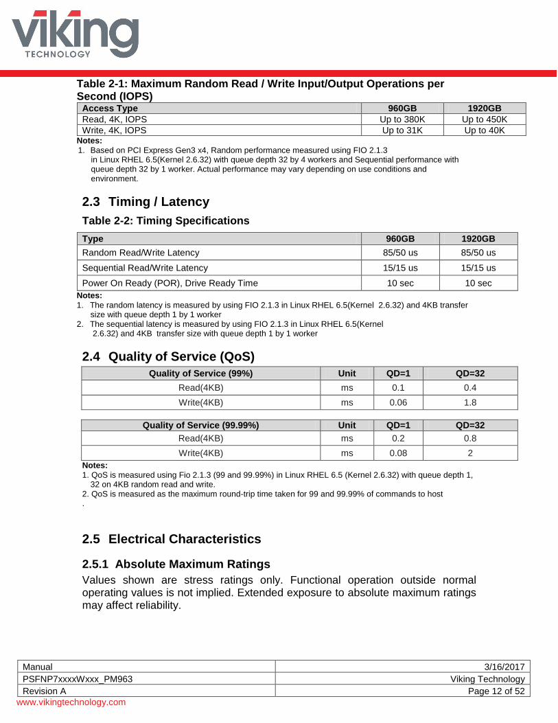
Table 2-1: Maximum Random Read / Write Input/Output Operations per Second (IOPS)
Access Type 960GB 1920GB
Read, 4K, IOPS Up to 380K Up to 450K
Write, 4K, IOPS Up to 31K Up to 40K Notes:
1. Based on PCI Express Gen3 x4, Random performance measured using FIO 2.1.3 in Linux RHEL 6.5(Kernel 2.6.32) with queue depth 32 by 4 workers and Sequential performance with queue depth 32 by 1 worker. Actual performance may vary depending on use conditions and environment.
2.3 Timing / Latency
Table 2-2: Timing Specifications
Type 960GB 1920GB
Random Read/Write Latency 85/50 us 85/50 us
Sequential Read/Write Latency 15/15 us 15/15 us
Power On Ready (POR), Drive Ready Time 10 sec 10 sec
Notes:
1. The random latency is measured by using FIO 2.1.3 in Linux RHEL 6.5(Kernel 2.6.32) and 4KB transfer size with queue depth 1 by 1 worker
2. The sequential latency is measured by using FIO 2.1.3 in Linux RHEL 6.5(Kernel 2.6.32) and 4KB transfer size with queue depth 1 by 1 worker
2.4 Quality of Service (QoS)
Quality of Service (99%) Unit QD=1 QD=32
Read(4KB) ms 0.1 0.4
Write(4KB) ms 0.06 1.8
Quality of Service (99.99%) Unit QD=1 QD=32
Read(4KB) ms 0.2 0.8
Write(4KB) ms 0.08 2
Notes:
1. QoS is measured using Fio 2.1.3 (99 and 99.99%) in Linux RHEL 6.5 (Kernel 2.6.32) with queue depth 1, 32 on 4KB random read and write.
2. QoS is measured as the maximum round-trip time taken for 99 and 99.99% of commands to host .
2.5 Electrical Characteristics
2.5.1 Absolute Maximum Ratings
Values shown are stress ratings only. Functional operation outside normal operating values is not implied. Extended exposure to absolute maximum ratings may affect reliability.
Manual 3/16/2017
PSFNP7xxxxWxxx_PM963 Viking Technology
Revision A Page 13 of 52
www.vikingtechnology.com
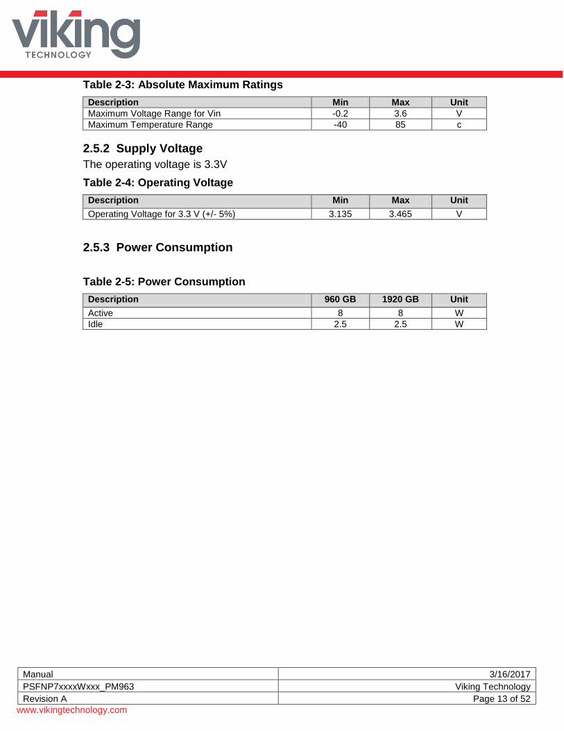
Table 2-3: Absolute Maximum Ratings
Description Min Max Unit
Maximum Voltage Range for Vin -0.2 3.6 V
Maximum Temperature Range -40 85 c
2.5.2 Supply Voltage
The operating voltage is 3.3V
Table 2-4: Operating Voltage
Description Min Max Unit
Operating Voltage for 3.3 V (+/- 5%) 3.135 3.465 V
2.5.3 Power Consumption
Table 2-5: Power Consumption
Description 960 GB 1920 GB Unit
Active 8 8 W
Idle 2.5 2.5 W
Manual 3/16/2017
PSFNP7xxxxWxxx_PM963 Viking Technology
Revision A Page 14 of 52
www.vikingtechnology.com
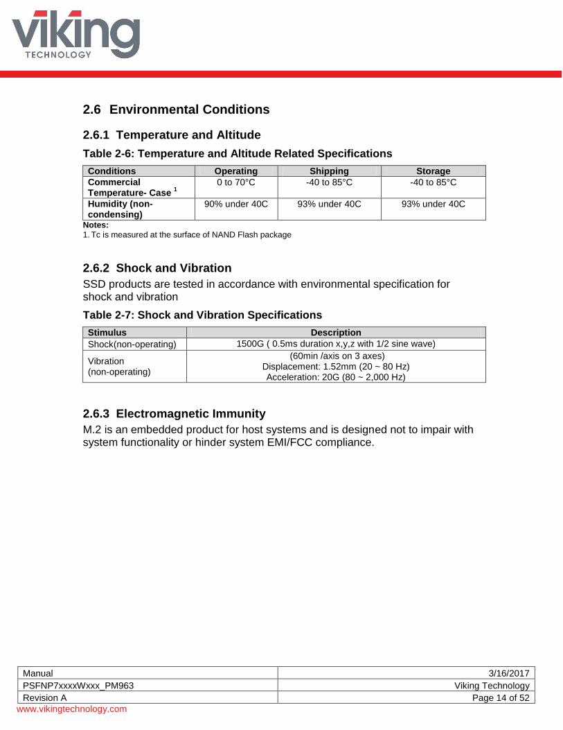
2.6 Environmental Conditions
2.6.1 Temperature and Altitude
Table 2-6: Temperature and Altitude Related Specifications
Conditions Operating Shipping Storage
Commercial Temperature- Case
1
0 to 70°C
-40 to 85°C
-40 to 85°C
Humidity (non-condensing)
90% under 40C 93% under 40C 93% under 40C
Notes: 1. Tc is measured at the surface of NAND Flash package
2.6.2 Shock and Vibration
SSD products are tested in accordance with environmental specification for shock and vibration
Table 2-7: Shock and Vibration Specifications
Stimulus Description
Shock(non-operating) 1500G ( 0.5ms duration x,y,z with 1/2 sine wave)
Vibration (non-operating)
(60min /axis on 3 axes) Displacement: 1.52mm (20 ~ 80 Hz) Acceleration: 20G (80 ~ 2,000 Hz)
2.6.3 Electromagnetic Immunity
M.2 is an embedded product for host systems and is designed not to impair with system functionality or hinder system EMI/FCC compliance.
Manual 3/16/2017
PSFNP7xxxxWxxx_PM963 Viking Technology
Revision A Page 15 of 52
www.vikingtechnology.com
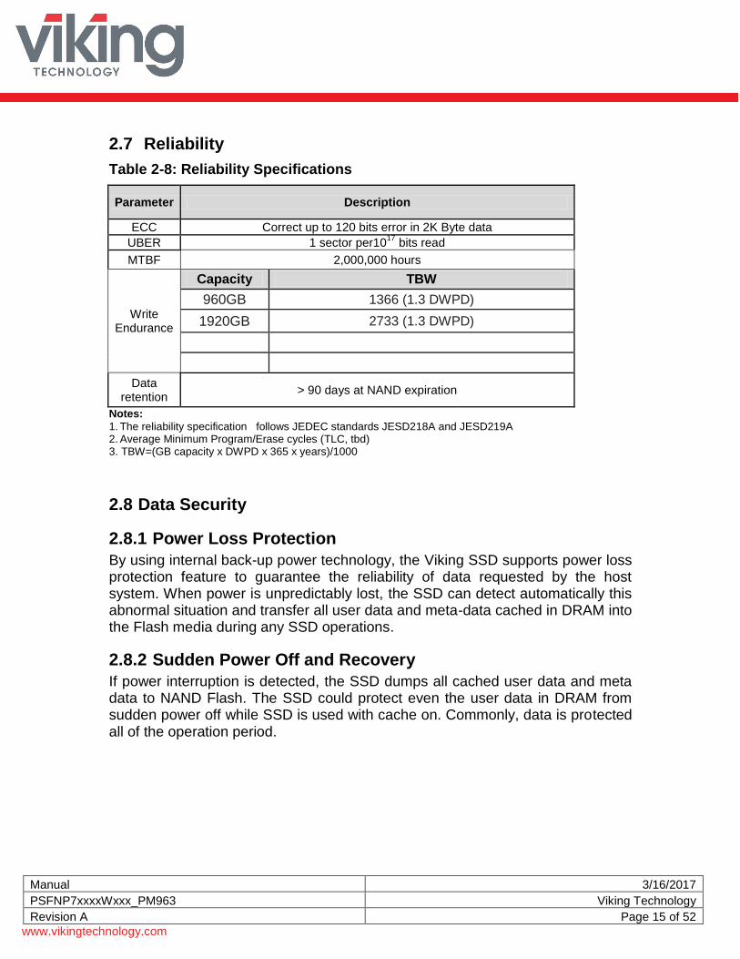
2.7 Reliability
Table 2-8: Reliability Specifications
Parameter Description
ECC Correct up to 120 bits error in 2K Byte data
UBER 1 sector per1017
bits read
MTBF 2,000,000 hours
Write Endurance
Capacity TBW
960GB 1366 (1.3 DWPD)
1920GB 2733 (1.3 DWPD)
Data
retention > 90 days at NAND expiration
Notes: 1. The reliability specification follows JEDEC standards JESD218A and JESD219A 2. Average Minimum Program/Erase cycles (TLC, tbd) 3. TBW=(GB capacity x DWPD x 365 x years)/1000
2.8 Data Security
2.8.1 Power Loss Protection
By using internal back-up power technology, the Viking SSD supports power loss protection feature to guarantee the reliability of data requested by the host system. When power is unpredictably lost, the SSD can detect automatically this abnormal situation and transfer all user data and meta-data cached in DRAM into the Flash media during any SSD operations.
2.8.2 Sudden Power Off and Recovery
If power interruption is detected, the SSD dumps all cached user data and meta data to NAND Flash. The SSD could protect even the user data in DRAM from sudden power off while SSD is used with cache on. Commonly, data is protected all of the operation period.
Manual 3/16/2017
PSFNP7xxxxWxxx_PM963 Viking Technology
Revision A Page 16 of 52
www.vikingtechnology.com
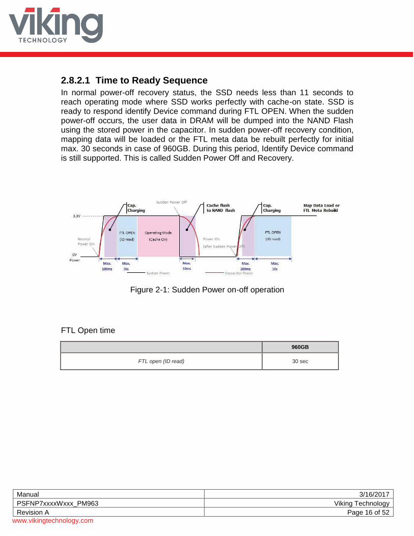
2.8.2.1 Time to Ready Sequence
In normal power-off recovery status, the SSD needs less than 11 seconds to reach operating mode where SSD works perfectly with cache-on state. SSD is ready to respond identify Device command during FTL OPEN. When the sudden power-off occurs, the user data in DRAM will be dumped into the NAND Flash using the stored power in the capacitor. In sudden power-off recovery condition, mapping data will be loaded or the FTL meta data be rebuilt perfectly for initial max. 30 seconds in case of 960GB. During this period, Identify Device command is still supported. This is called Sudden Power Off and Recovery.
Figure 2-1: Sudden Power on-off operation
FTL Open time
960GB
FTL open (ID read) 30 sec
Manual 3/16/2017
PSFNP7xxxxWxxx_PM963 Viking Technology
Revision A Page 17 of 52
www.vikingtechnology.com
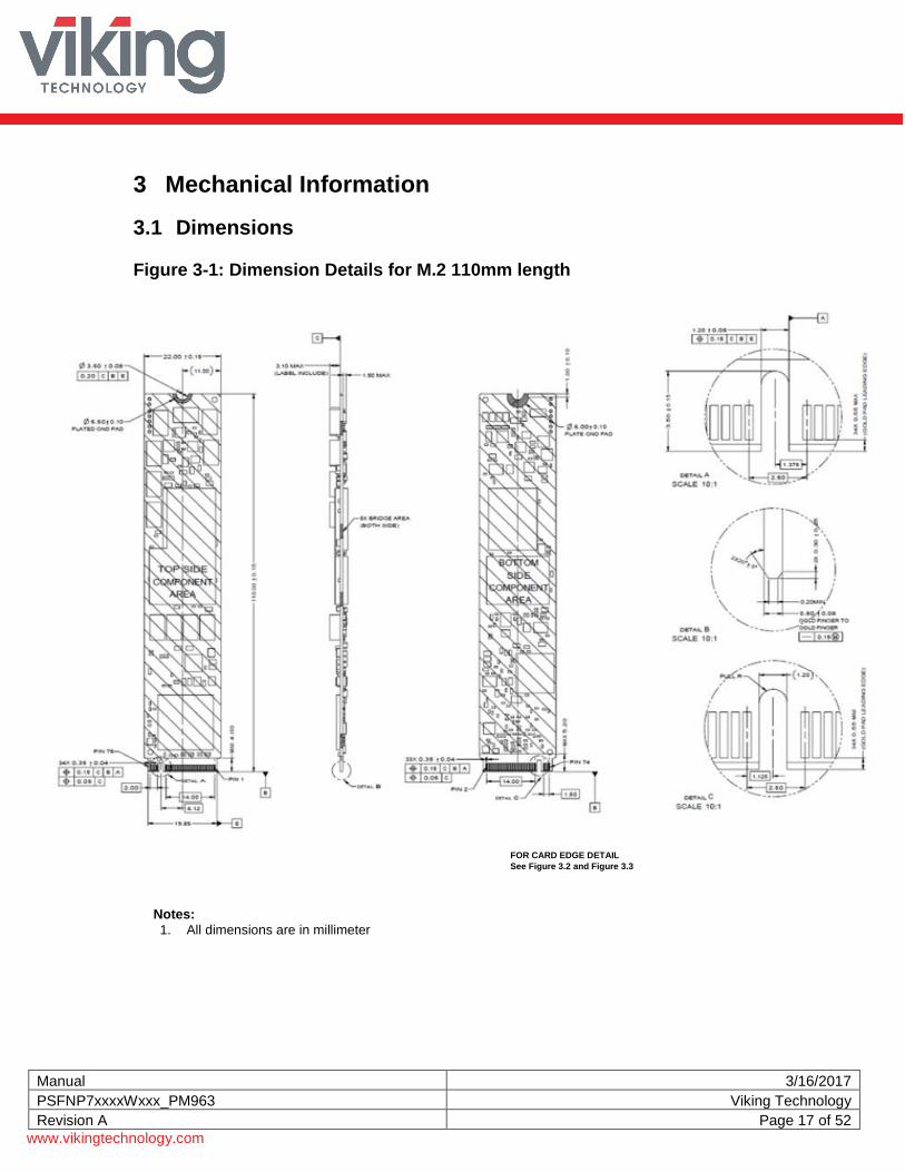
3 Mechanical Information
3.1 Dimensions
Figure 3-1: Dimension Details for M.2 110mm length
Notes:
1. All dimensions are in millimeter
FOR CARD EDGE DETAIL
See Figure 3.2 and Figure 3.3
Manual 3/16/2017
PSFNP7xxxxWxxx_PM963 Viking Technology
Revision A Page 18 of 52
www.vikingtechnology.com
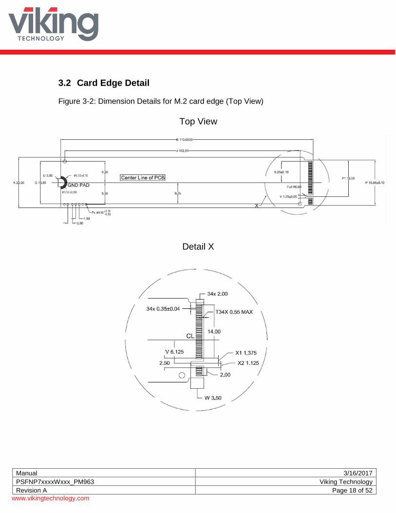
3.2 Card Edge Detail
Figure 3-2: Dimension Details for M.2 card edge (Top View)
Top View
Detail X
Manual 3/16/2017
PSFNP7xxxxWxxx_PM963 Viking Technology
Revision A Page 19 of 52
www.vikingtechnology.com
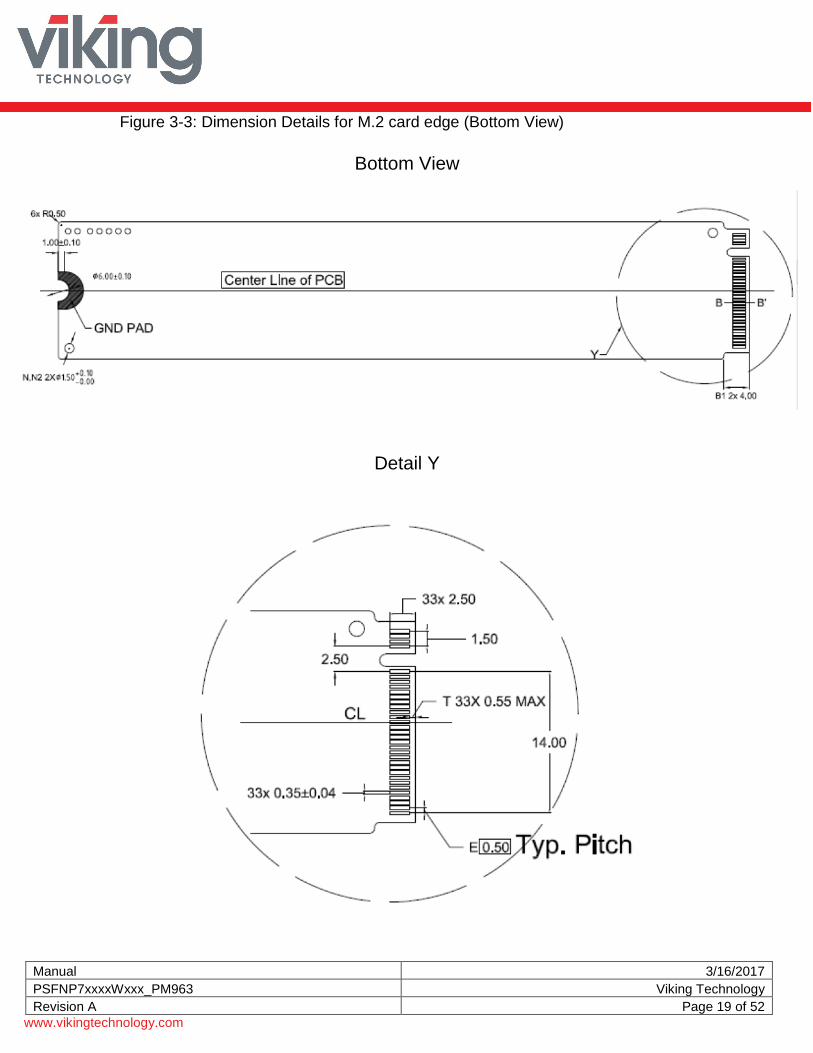
Figure 3-3: Dimension Details for M.2 card edge (Bottom View)
Bottom View
Detail Y
Manual 3/16/2017
PSFNP7xxxxWxxx_PM963 Viking Technology
Revision A Page 20 of 52
www.vikingtechnology.com
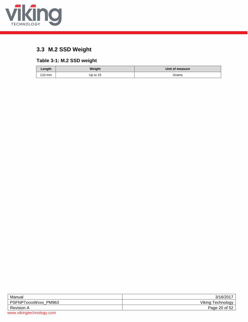
3.3 M.2 SSD Weight
Table 3-1: M.2 SSD weight
Length Weight Unit of measure
110 mm Up to 15 Grams
Manual 3/16/2017
PSFNP7xxxxWxxx_PM963 Viking Technology
Revision A Page 21 of 52
www.vikingtechnology.com
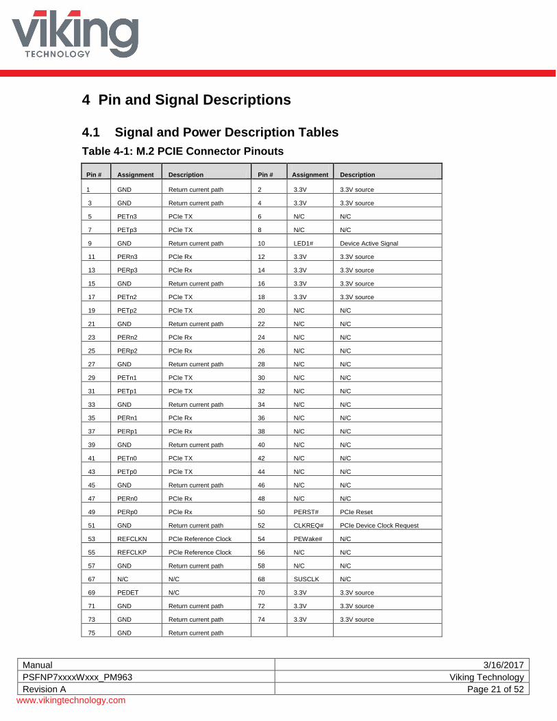
4 Pin and Signal Descriptions
4.1 Signal and Power Description Tables
Table 4-1: M.2 PCIE Connector Pinouts
Pin # Assignment Description Pin # Assignment Description
1 GND Return current path 2 3.3V 3.3V source
3 GND Return current path 4 3.3V 3.3V source
5 PETn3 PCIe TX 6 N/C N/C
7 PETp3 PCIe TX 8 N/C N/C
9 GND Return current path 10 LED1# Device Active Signal
11 PERn3 PCIe Rx 12 3.3V 3.3V source
13 PERp3 PCIe Rx 14 3.3V 3.3V source
15 GND Return current path 16 3.3V 3.3V source
17 PETn2 PCIe TX 18 3.3V 3.3V source
19 PETp2 PCIe TX 20 N/C N/C
21 GND Return current path 22 N/C N/C
23 PERn2 PCIe Rx 24 N/C N/C
25 PERp2 PCIe Rx 26 N/C N/C
27 GND Return current path 28 N/C N/C
29 PETn1 PCIe TX 30 N/C N/C
31 PETp1 PCIe TX 32 N/C N/C
33 GND Return current path 34 N/C N/C
35 PERn1 PCIe Rx 36 N/C N/C
37 PERp1 PCIe Rx 38 N/C N/C
39 GND Return current path 40 N/C N/C
41 PETn0 PCIe TX 42 N/C N/C
43 PETp0 PCIe TX 44 N/C N/C
45 GND Return current path 46 N/C N/C
47 PERn0 PCIe Rx 48 N/C N/C
49 PERp0 PCIe Rx 50 PERST# PCIe Reset
51 GND Return current path 52 CLKREQ# PCIe Device Clock Request
53 REFCLKN PCIe Reference Clock 54 PEWake# N/C
55 REFCLKP PCIe Reference Clock 56 N/C N/C
57 GND Return current path 58 N/C N/C
67 N/C N/C 68 SUSCLK N/C
69 PEDET N/C 70 3.3V 3.3V source
71 GND Return current path 72 3.3V 3.3V source
73 GND Return current path 74 3.3V 3.3V source
75 GND Return current path
Manual 3/16/2017
PSFNP7xxxxWxxx_PM963 Viking Technology
Revision A Page 22 of 52
www.vikingtechnology.com
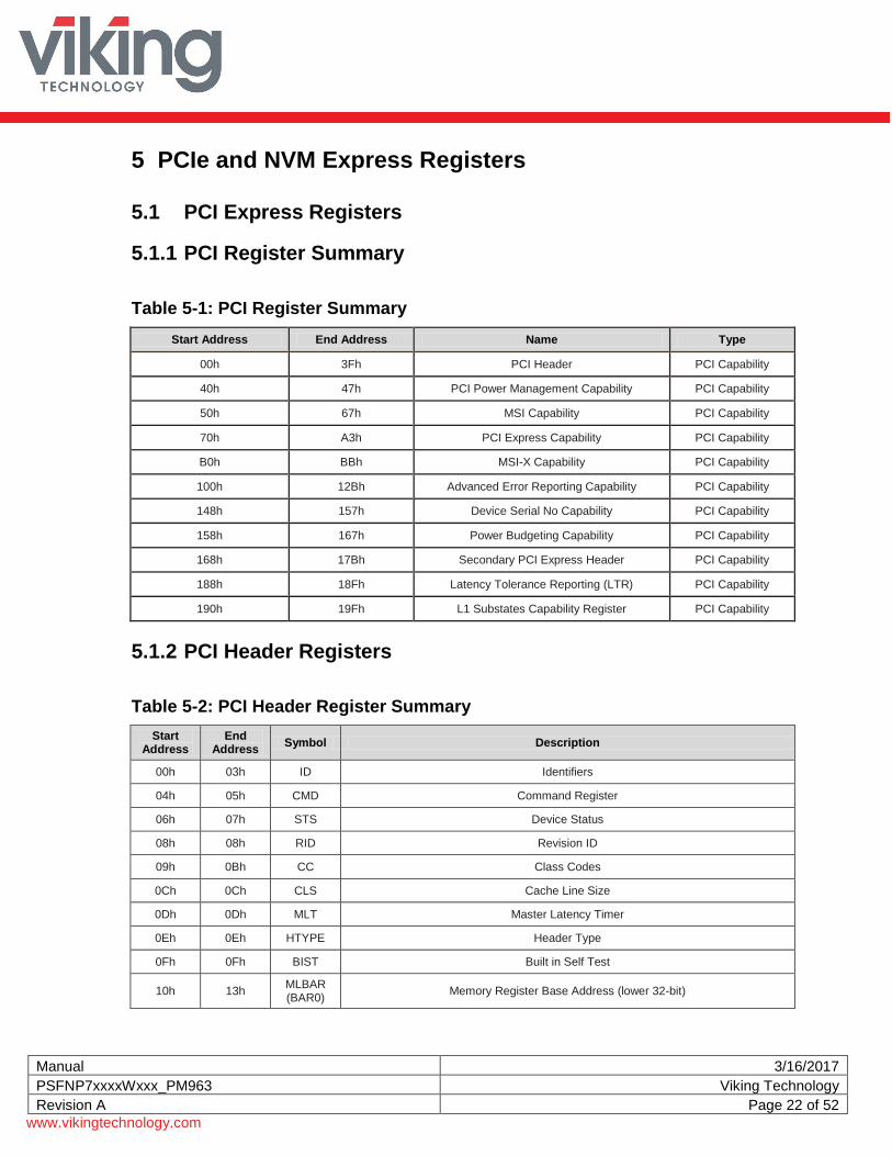
5 PCIe and NVM Express Registers
5.1 PCI Express Registers
5.1.1 PCI Register Summary
Table 5-1: PCI Register Summary
Start Address End Address Name Type
00h 3Fh PCI Header PCI Capability
40h 47h PCI Power Management Capability PCI Capability
50h 67h MSI Capability PCI Capability
70h A3h PCI Express Capability PCI Capability
B0h BBh MSI-X Capability PCI Capability
100h 12Bh Advanced Error Reporting Capability PCI Capability
148h 157h Device Serial No Capability PCI Capability
158h 167h Power Budgeting Capability PCI Capability
168h 17Bh Secondary PCI Express Header PCI Capability
188h 18Fh Latency Tolerance Reporting (LTR) PCI Capability
190h 19Fh L1 Substates Capability Register PCI Capability
5.1.2 PCI Header Registers
Table 5-2: PCI Header Register Summary
Start Address
End Address
Symbol Description
00h 03h ID Identifiers
04h 05h CMD Command Register
06h 07h STS Device Status
08h 08h RID Revision ID
09h 0Bh CC Class Codes
0Ch 0Ch CLS Cache Line Size
0Dh 0Dh MLT Master Latency Timer
0Eh 0Eh HTYPE Header Type
0Fh 0Fh BIST Built in Self Test
10h 13h MLBAR (BAR0)
Memory Register Base Address (lower 32-bit)
Manual 3/16/2017
PSFNP7xxxxWxxx_PM963 Viking Technology
Revision A Page 23 of 52
www.vikingtechnology.com
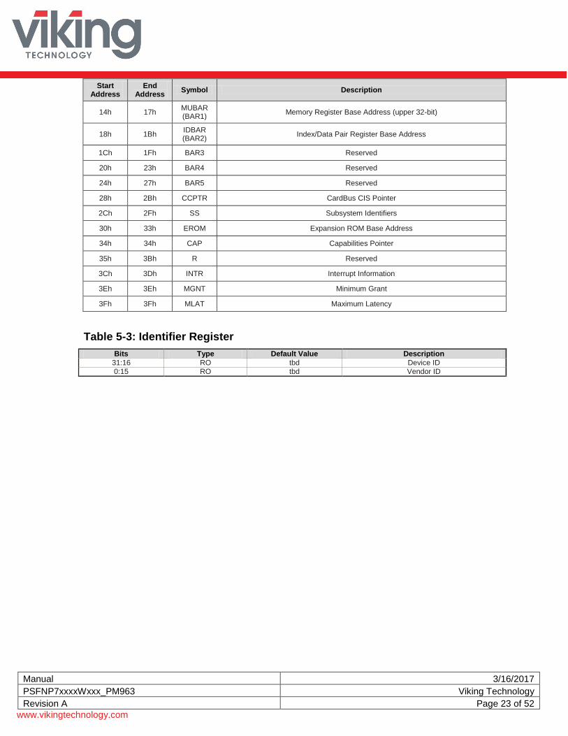
Start Address
End Address
Symbol Description
14h 17h MUBAR (BAR1)
Memory Register Base Address (upper 32-bit)
18h 1Bh IDBAR (BAR2)
Index/Data Pair Register Base Address
1Ch 1Fh BAR3 Reserved
20h 23h BAR4 Reserved
24h 27h BAR5 Reserved
28h 2Bh CCPTR CardBus CIS Pointer
2Ch 2Fh SS Subsystem Identifiers
30h 33h EROM Expansion ROM Base Address
34h 34h CAP Capabilities Pointer
35h 3Bh R Reserved
3Ch 3Dh INTR Interrupt Information
3Eh 3Eh MGNT Minimum Grant
3Fh 3Fh MLAT Maximum Latency
Table 5-3: Identifier Register
Bits Type Default Value Description
31:16 RO tbd Device ID
0:15 RO tbd Vendor ID
Manual 3/16/2017
PSFNP7xxxxWxxx_PM963 Viking Technology
Revision A Page 24 of 52
www.vikingtechnology.com
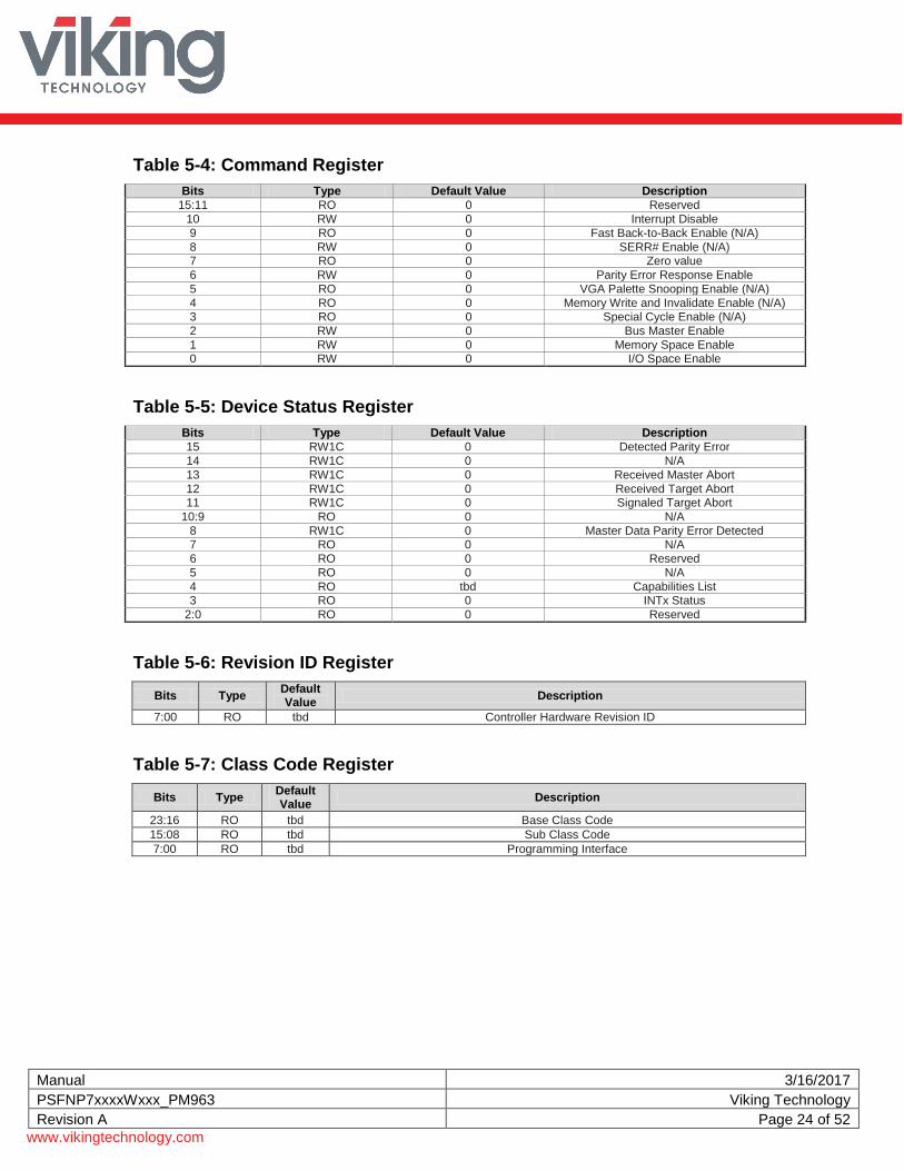
Table 5-4: Command Register
Bits Type Default Value Description
15:11 RO 0 Reserved
10 RW 0 Interrupt Disable
9 RO 0 Fast Back-to-Back Enable (N/A)
8 RW 0 SERR# Enable (N/A) 7 RO 0 Zero value
6 RW 0 Parity Error Response Enable
5 RO 0 VGA Palette Snooping Enable (N/A)
4 RO 0 Memory Write and Invalidate Enable (N/A) 3 RO 0 Special Cycle Enable (N/A)
2 RW 0 Bus Master Enable
1 RW 0 Memory Space Enable 0 RW 0 I/O Space Enable
Table 5-5: Device Status Register
Bits Type Default Value Description
15 RW1C 0 Detected Parity Error
14 RW1C 0 N/A
13 RW1C 0 Received Master Abort
12 RW1C 0 Received Target Abort 11 RW1C 0 Signaled Target Abort
10:9 RO 0 N/A
8 RW1C 0 Master Data Parity Error Detected 7 RO 0 N/A
6 RO 0 Reserved
5 RO 0 N/A
4 RO tbd Capabilities List 3 RO 0 INTx Status
2:0 RO 0 Reserved
Table 5-6: Revision ID Register
Bits Type Default Value
Description
7:00 RO tbd Controller Hardware Revision ID
Table 5-7: Class Code Register
Bits Type Default Value
Description
23:16 RO tbd Base Class Code
15:08 RO tbd Sub Class Code
7:00 RO tbd Programming Interface
Manual 3/16/2017
PSFNP7xxxxWxxx_PM963 Viking Technology
Revision A Page 25 of 52
www.vikingtechnology.com
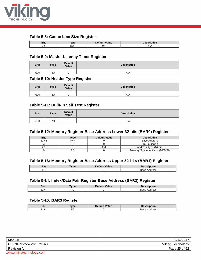
Table 5-8: Cache Line Size Register
Bits Type Default Value Description
7:0 RW 0h N/A
Table 5-9: Master Latency Timer Register
Bits Type Default Value
Description
7:00 RO 0 N/A
Table 5-10: Header Type Register
Bits Type Default Value
Description
7:00 RO 0 N/A
Table 5-11: Built-in Self Test Register
Bits Type Default Value
Description
7:00 RO 0 N/A
Table 5-12: Memory Register Base Address Lower 32-bits (BAR0) Register
Bits Type Default Value Description
31:04 RW 0 Base Address
3 RO 0 Pre-Fetchable
2:1 RO tbd Address Type (64-bit)
0 RO 0 Memory Space Indicator (MEMSI)
Table 5-13: Memory Register Base Address Upper 32-bits (BAR1) Register
Bits Type Default Value Description
31:0 RO 0 Base Address
Table 5-14: Index/Data Pair Register Base Address (BAR2) Register
Bits Type Default Value Description
31:0 RO 0 Base Address
Table 5-15: BAR3 Register
Bits Type Default Value Description
31:0 RO 0 Base Address
Manual 3/16/2017
PSFNP7xxxxWxxx_PM963 Viking Technology
Revision A Page 26 of 52
www.vikingtechnology.com
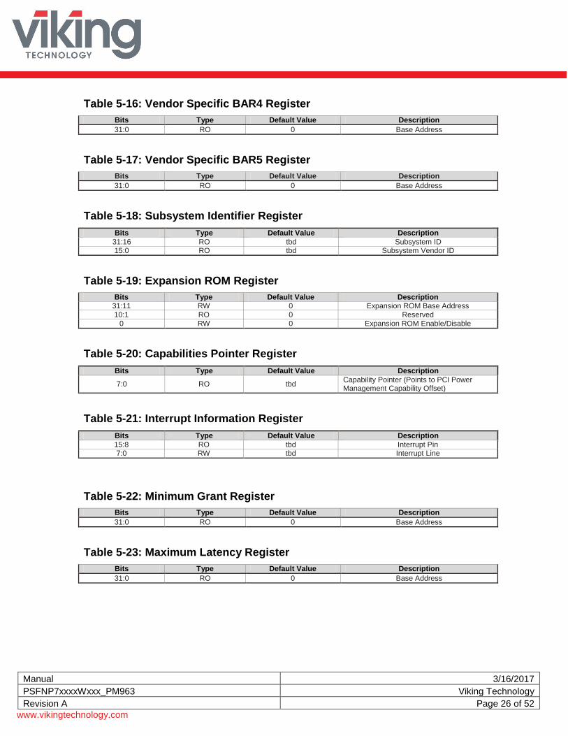
Table 5-16: Vendor Specific BAR4 Register
Bits Type Default Value Description
31:0 RO 0 Base Address
Table 5-17: Vendor Specific BAR5 Register
Bits Type Default Value Description
31:0 RO 0 Base Address
Table 5-18: Subsystem Identifier Register
Bits Type Default Value Description
31:16 RO tbd Subsystem ID 15:0 RO tbd Subsystem Vendor ID
Table 5-19: Expansion ROM Register
Bits Type Default Value Description
31:11 RW 0 Expansion ROM Base Address
10:1 RO 0 Reserved
0 RW 0 Expansion ROM Enable/Disable
Table 5-20: Capabilities Pointer Register
Bits Type Default Value Description
7:0 RO tbd Capability Pointer (Points to PCI Power Management Capability Offset)
Table 5-21: Interrupt Information Register
Bits Type Default Value Description
15:8 RO tbd Interrupt Pin 7:0 RW tbd Interrupt Line
Table 5-22: Minimum Grant Register
Bits Type Default Value Description
31:0 RO 0 Base Address
Table 5-23: Maximum Latency Register
Bits Type Default Value Description
31:0 RO 0 Base Address
Manual 3/16/2017
PSFNP7xxxxWxxx_PM963 Viking Technology
Revision A Page 27 of 52
www.vikingtechnology.com
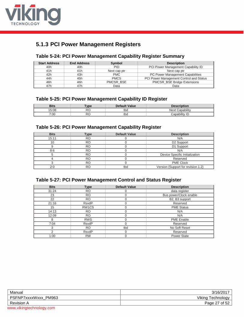
5.1.3 PCI Power Management Registers
Table 5-24: PCI Power Management Capability Register Summary
Start Address End Address Symbol Description
40h 40h PID PCI Power Management Capability ID
41h 41h Next cap ptr Next cap ptr
42h 43h PMC PC Power Management Capabilities
44h 45h PMCS PCI Power Management Control and Status 46h 46h PMCSR_BSE PMCSR_BSE Bridge Extensions
47h 47h Data Data
Table 5-25: PCI Power Management Capability ID Register
Bits Type Default Value Description
15:08 RO tbd Next Capability
7:00 RO tbd Capability ID
Table 5-26: PCI Power Management Capability Register
Bits Type Default Value Description
15:11 RO 0 N/A
10 RO 0 D2 Support
9 RO 0 D1 Support
8:6 RO 0 N/A
5 RO 0 Device Specific Initialization
4 RO 0 Reserved
3 RO 0 PME Clock
2:0 RO tbd Version (Support for revision 1.2)
Table 5-27: PCI Power Management Control and Status Register
Bits Type Default Value Description
31:24 RO 0 data register
23 RO 0 Bus power/Clock enable
22 RO 0 B2, B3 support
21:16 RsvdP 0 Reserved
15 RW1CS 0 PME Status
14:13 RO 0 N/A
12:09 RO 0 N/A
8 RWS 0 PME Enable
7:04 RsvdP 0 Reserved
3 RO tbd No Soft Reset
2 RsvdP 0 Reserved
1:00 RW 0 Power State
Manual 3/16/2017
PSFNP7xxxxWxxx_PM963 Viking Technology
Revision A Page 28 of 52
www.vikingtechnology.com
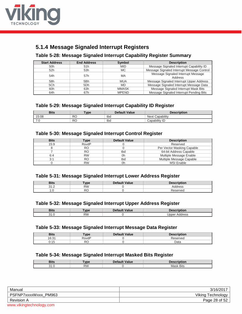
5.1.4 Message Signaled Interrupt Registers
Table 5-28: Message Signaled Interrupt Capability Register Summary
Start Address End Address Symbol Description
50h 51h MID Message Signaled Interrupt Capability ID 52h 53h MC Message Signaled Interrupt Message Control
54h 57h MA Message Signaled Interrupt Message
Address
58h 5Bh MUA Message Signaled Interrupt Upper Address 5Ch 5Dh MD Message Signaled Interrupt Message Data
60h 63h MMASK Message Signaled Interrupt Mask Bits
64h 67h MPEND Message Signaled Interrupt Pending Bits
Table 5-29: Message Signaled Interrupt Capability ID Register
Bits Type Default Value Description
15:08 RO tbd Next Capability
7:0 RO tbd Capability ID
Table 5-30: Message Signaled Interrupt Control Register
Bits Type Default Value Description
15:9 RsvdP 0 Reserved 8 RO 0 Per Vector Masking Capable
7 RO tbd 64-bit Address Capable
6:4 RW 0h Multiple Message Enable
3:1 RO tbd Multiple Message Capable 0 RW 0h MSI Enable
Table 5-31: Message Signaled Interrupt Lower Address Register
Bits Type Default Value Description
31:2 RW 0 Address
1:0 RO 0 Reserved
Table 5-32: Message Signaled Interrupt Upper Address Register
Bits Type Default Value Description
31:0 RW 0 Upper Address
Table 5-33: Message Signaled Interrupt Message Data Register
Bits Type Default Value Description
16:31 RsvdP 0 Reserved
0:15 RO 0 Data
Table 5-34: Message Signaled Interrupt Masked Bits Register
Bits Type Default Value Description
31:0 RW 0 Mask Bits
Manual 3/16/2017
PSFNP7xxxxWxxx_PM963 Viking Technology
Revision A Page 29 of 52
www.vikingtechnology.com
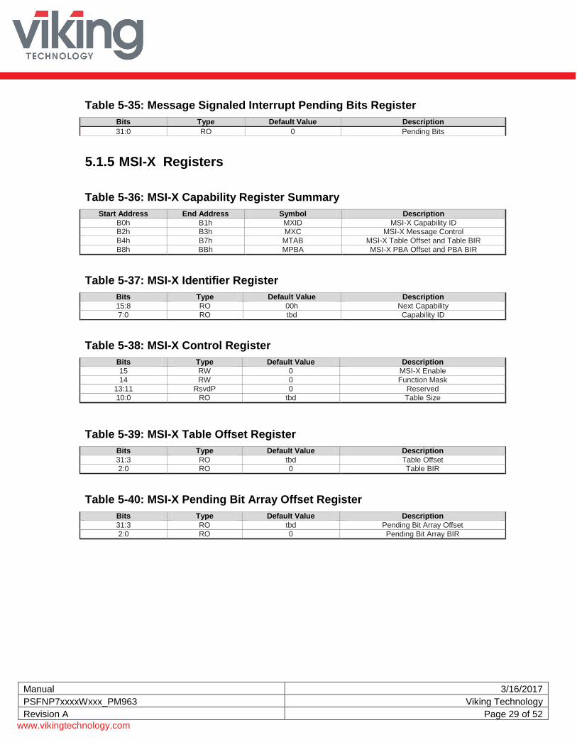
Table 5-35: Message Signaled Interrupt Pending Bits Register
Bits Type Default Value Description
31:0 RO 0 Pending Bits
5.1.5 MSI-X Registers
Table 5-36: MSI-X Capability Register Summary
Start Address End Address Symbol Description
B0h B1h MXID MSI-X Capability ID B2h B3h MXC MSI-X Message Control
B4h B7h MTAB MSI-X Table Offset and Table BIR
B8h BBh MPBA MSI-X PBA Offset and PBA BIR
Table 5-37: MSI-X Identifier Register
Bits Type Default Value Description
15:8 RO 00h Next Capability
7:0 RO tbd Capability ID
Table 5-38: MSI-X Control Register
Bits Type Default Value Description
15 RW 0 MSI-X Enable
14 RW 0 Function Mask
13:11 RsvdP 0 Reserved
10:0 RO tbd Table Size
Table 5-39: MSI-X Table Offset Register
Bits Type Default Value Description
31:3 RO tbd Table Offset 2:0 RO 0 Table BIR
Table 5-40: MSI-X Pending Bit Array Offset Register
Bits Type Default Value Description
31:3 RO tbd Pending Bit Array Offset
2:0 RO 0 Pending Bit Array BIR
Manual 3/16/2017
PSFNP7xxxxWxxx_PM963 Viking Technology
Revision A Page 30 of 52
www.vikingtechnology.com
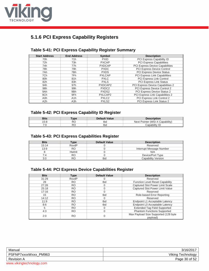
5.1.6 PCI Express Capability Registers
Table 5-41: PCI Express Capability Register Summary
Start Address End Address Symbol Description
70h 71h PXID PCI Express Capability ID
72h 73h PXCAP PCI Express Capabilities
74h 77h PXDCAP PCI Express Device Capabilities 78h 79h PXDC PCI Express Device Control
7Ah 7Bh PXDS PCI Express Device Status
7Ch 7Fh PXLCAP PCI Express Link Capabilities
80h 81h PXLC PCI Express Link Control 82h 83h PXLS PCI Express Link Status
94h 97h PXDCAP2 PCI Express Device Capabilities 2
98h 99h PXDC2 PCI Express Device Control 2
9Ah 9Bh PXDS2 PCI Express Device Status 2 9Ch 9Fh PXLCAP2 PCI Express Link Capabilities 2
A0h A1h PXLC2 PCI Express Link Control 2
A2h A3h PXLS2 PCI Express Link Status 2
Table 5-42: PCI Express Capability ID Register
Bits Type Default Value Description
15:8 RO tbd Next Pointer (MSI-X Capability) 7:0 RO tbd Capability ID
Table 5-43: PCI Express Capabilities Register
Bits Type Default Value Description
15:14 RsvdP 0 Reserved
13:9 RO 0 Interrupt Message Number
8 HwInit 0 N/A
7:4 RO 0 Device/Port Type 3:0 RO tbd Capability Version
Table 5-44: PCI Express Device Capabilities Register
Bits Type Default Value Description
31:29 RsvdP 0 Reserved
28 RO tbd Function Level Reset Capability
27:26 RO 0 Captured Slot Power Limit Scale 25:18 RO 0 Captured Slot Power Limit Value
17:16 RO 0 Reserved
15 RO tbd Role-based Error Reporting
14:12 RO 0 Reserved 11:9 RO tbd Endpoint L1 Acceptable Latency
8:6 RO tbd Endpoint L0 Acceptable Latency
5 RO 0 Extended Tag Field Supported
4:3 RO 0 Phantom Functions Supported
2:0 RO 0 Max Payload Size Supported (128 byte
payload)
Manual 3/16/2017
PSFNP7xxxxWxxx_PM963 Viking Technology
Revision A Page 31 of 52
www.vikingtechnology.com
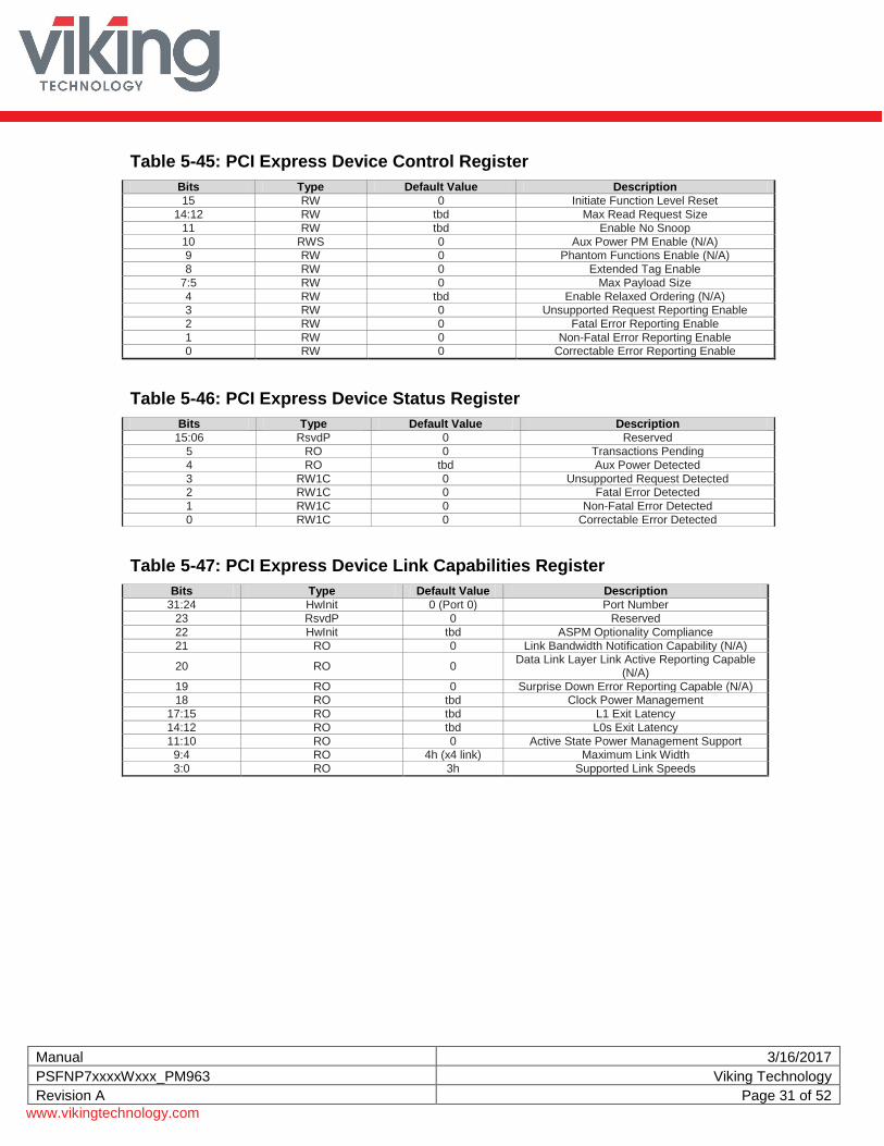
Table 5-45: PCI Express Device Control Register
Bits Type Default Value Description
15 RW 0 Initiate Function Level Reset
14:12 RW tbd Max Read Request Size
11 RW tbd Enable No Snoop
10 RWS 0 Aux Power PM Enable (N/A) 9 RW 0 Phantom Functions Enable (N/A)
8 RW 0 Extended Tag Enable
7:5 RW 0 Max Payload Size
4 RW tbd Enable Relaxed Ordering (N/A) 3 RW 0 Unsupported Request Reporting Enable
2 RW 0 Fatal Error Reporting Enable
1 RW 0 Non-Fatal Error Reporting Enable 0 RW 0 Correctable Error Reporting Enable
Table 5-46: PCI Express Device Status Register
Bits Type Default Value Description
15:06 RsvdP 0 Reserved
5 RO 0 Transactions Pending
4 RO tbd Aux Power Detected
3 RW1C 0 Unsupported Request Detected 2 RW1C 0 Fatal Error Detected
1 RW1C 0 Non-Fatal Error Detected
0 RW1C 0 Correctable Error Detected
Table 5-47: PCI Express Device Link Capabilities Register
Bits Type Default Value Description
31:24 HwInit 0 (Port 0) Port Number
23 RsvdP 0 Reserved
22 HwInit tbd ASPM Optionality Compliance
21 RO 0 Link Bandwidth Notification Capability (N/A)
20 RO 0 Data Link Layer Link Active Reporting Capable
(N/A)
19 RO 0 Surprise Down Error Reporting Capable (N/A) 18 RO tbd Clock Power Management
17:15 RO tbd L1 Exit Latency
14:12 RO tbd L0s Exit Latency
11:10 RO 0 Active State Power Management Support 9:4 RO 4h (x4 link) Maximum Link Width
3:0 RO 3h Supported Link Speeds
Manual 3/16/2017
PSFNP7xxxxWxxx_PM963 Viking Technology
Revision A Page 32 of 52
www.vikingtechnology.com
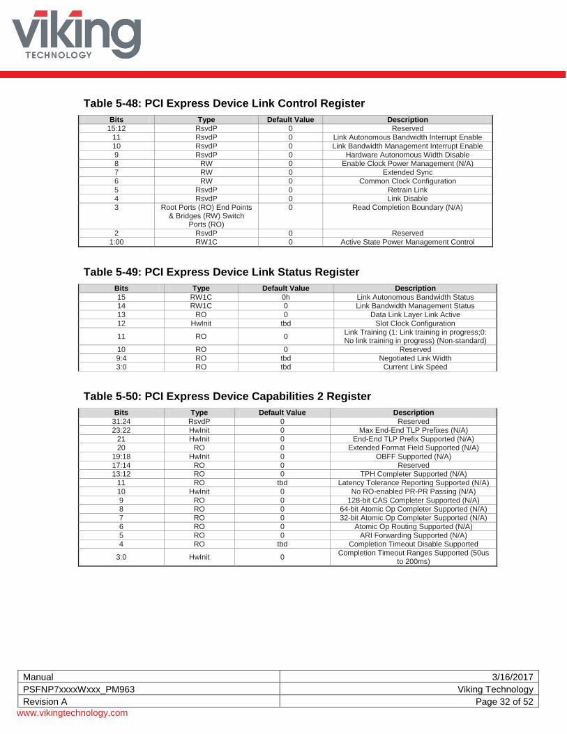
Table 5-48: PCI Express Device Link Control Register
Bits Type Default Value Description
15:12 RsvdP 0 Reserved
11 RsvdP 0 Link Autonomous Bandwidth Interrupt Enable
10 RsvdP 0 Link Bandwidth Management Interrupt Enable
9 RsvdP 0 Hardware Autonomous Width Disable 8 RW 0 Enable Clock Power Management (N/A)
7 RW 0 Extended Sync
6 RW 0 Common Clock Configuration
5 RsvdP 0 Retrain Link 4 RsvdP 0 Link Disable
3 Root Ports (RO) End Points & Bridges (RW) Switch
Ports (RO)
0 Read Completion Boundary (N/A)
2 RsvdP 0 Reserved
1:00 RW1C 0 Active State Power Management Control
Table 5-49: PCI Express Device Link Status Register
Bits Type Default Value Description
15 RW1C 0h Link Autonomous Bandwidth Status 14 RW1C 0 Link Bandwidth Management Status
13 RO 0 Data Link Layer Link Active
12 HwInit tbd Slot Clock Configuration
11 RO 0 Link Training (1: Link training in progress;0: No link training in progress) (Non-standard)
10 RO 0 Reserved
9:4 RO tbd Negotiated Link Width 3:0 RO tbd Current Link Speed
Table 5-50: PCI Express Device Capabilities 2 Register
Bits Type Default Value Description
31:24 RsvdP 0 Reserved
23:22 HwInit 0 Max End-End TLP Prefixes (N/A)
21 HwInit 0 End-End TLP Prefix Supported (N/A) 20 RO 0 Extended Format Field Supported (N/A)
19:18 HwInit 0 OBFF Supported (N/A)
17:14 RO 0 Reserved 13:12 RO 0 TPH Completer Supported (N/A)
11 RO tbd Latency Tolerance Reporting Supported (N/A)
10 HwInit 0 No RO-enabled PR-PR Passing (N/A)
9 RO 0 128-bit CAS Completer Supported (N/A) 8 RO 0 64-bit Atomic Op Completer Supported (N/A)
7 RO 0 32-bit Atomic Op Completer Supported (N/A)
6 RO 0 Atomic Op Routing Supported (N/A)
5 RO 0 ARI Forwarding Supported (N/A) 4 RO tbd Completion Timeout Disable Supported
3:0 HwInit 0 Completion Timeout Ranges Supported (50us
to 200ms)
Manual 3/16/2017
PSFNP7xxxxWxxx_PM963 Viking Technology
Revision A Page 33 of 52
www.vikingtechnology.com
Table 5-51: PCI Express Device Control 2 Register
Bits Type Default Value Description
15 RsvdP 0 End-to-end TLP Prefix Blocking (N/A)
14:13 RW/RsvdP 0 OBFF Enable (N/A)
12:11 RsvdP 0 Reserved
10 RW/RsvdP 0 Latency Tolerance Reporting Mechanism
Enable (N/A)
9 RW 0 IDO Completion Enable
8 RW 0 IDO Request Enable 7 RW 0 AtomicOp Egress Blocking
6 RW 0 AtomicOp Requester Enable
5 RW 0 ARI Forwarding Enable
4 RW 0 Completion Timeout Disable
3:0 RW 0 Completion Timeout Value (0h - 50 ȝs; 1h - 100 ȝs; 2h - 2 ms; 5h - 50 ms; 6h - 200 ms; others -
reserved )
Table 5-52: PCI Express Device Status 2 Register
Bits Type Default Value Description
15:0 RsvdZ 0 Reserved
Table 5-53: PCI Express Link Capabilities 2 Register
Bits Type Default Value Description
31:9 RsvdP 0 Reserved
8 RO 0 Cross-Link Supported (N/A)
7:1 RO tbd Supported Link Speeds 001b: 2.5 GT/s (Gen 1) 010b: 5.0 GT/s (Gen 2) 100b: 8 GT/s (Gen 3)
0 RsvdP 0 Reserved
Table 5-54: PCI Express Link Control 2 Register
Bits Type Default Value Description
15:12 RWS/RsvdP 0 Compliance De-emphasis
11 RWS/RsvdP 0 Compliance SOS 10 RWS/RsvdP 0 Enter Modified Compliance
9:7 RWS/RsvdP 0 Transmit Margin
6 HwInit 0 Select De-Emphasis 5 RWS/RsvdP 0 Hardware Autonomous Speed Disable
4 RWS/RsvdP 0 Enter Compliance
3:0 RWS/RsvdP tbd Target Link Speed 1h: 2.5 GT/s (Gen 1) 2h: 5.0
GT/s (Gen 2) 3h: 8 GT/s (Gen 3)
Table 5-55: PCI Express Link Status 2 Register
Bits Type Default Value Description
15:6 RsvdP 0 Reserved
5 RW1CS 0 Link Equalization Request
4 ROS 0 Equalization Phase 3 Successful 3 ROS 0 Equalization Phase 2 Successful
2 ROS 0 Equalization Phase 1 Successful
1 ROS 0 Equalization Complete
0 RO tbd Current De-Emphasis
Manual 3/16/2017
PSFNP7xxxxWxxx_PM963 Viking Technology
Revision A Page 34 of 52
www.vikingtechnology.com
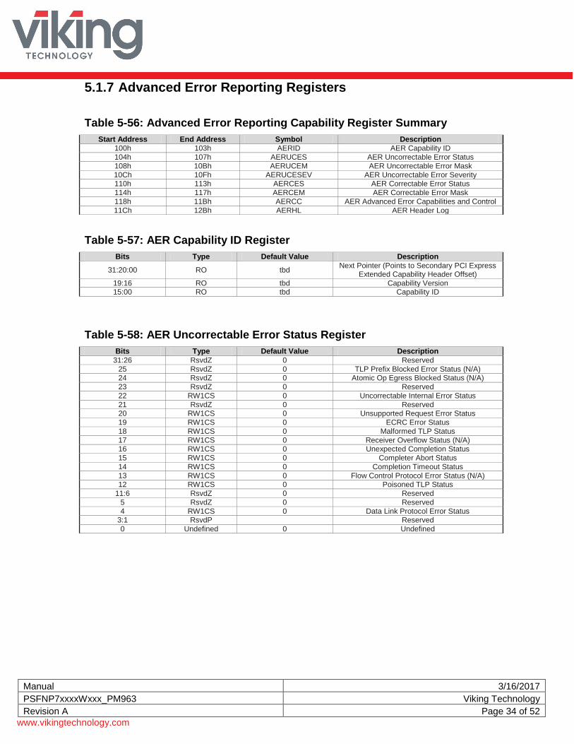
5.1.7 Advanced Error Reporting Registers
Table 5-56: Advanced Error Reporting Capability Register Summary
Start Address End Address Symbol Description
100h 103h AERID AER Capability ID
104h 107h AERUCES AER Uncorrectable Error Status
108h 10Bh AERUCEM AER Uncorrectable Error Mask
10Ch 10Fh AERUCESEV AER Uncorrectable Error Severity 110h 113h AERCES AER Correctable Error Status
114h 117h AERCEM AER Correctable Error Mask
118h 11Bh AERCC AER Advanced Error Capabilities and Control
11Ch 12Bh AERHL AER Header Log
Table 5-57: AER Capability ID Register
Bits Type Default Value Description
31:20:00 RO tbd Next Pointer (Points to Secondary PCI Express
Extended Capability Header Offset)
19:16 RO tbd Capability Version 15:00 RO tbd Capability ID
Table 5-58: AER Uncorrectable Error Status Register
Bits Type Default Value Description
31:26 RsvdZ 0 Reserved
25 RsvdZ 0 TLP Prefix Blocked Error Status (N/A) 24 RsvdZ 0 Atomic Op Egress Blocked Status (N/A)
23 RsvdZ 0 Reserved
22 RW1CS 0 Uncorrectable Internal Error Status
21 RsvdZ 0 Reserved 20 RW1CS 0 Unsupported Request Error Status
19 RW1CS 0 ECRC Error Status
18 RW1CS 0 Malformed TLP Status
17 RW1CS 0 Receiver Overflow Status (N/A) 16 RW1CS 0 Unexpected Completion Status
15 RW1CS 0 Completer Abort Status
14 RW1CS 0 Completion Timeout Status
13 RW1CS 0 Flow Control Protocol Error Status (N/A) 12 RW1CS 0 Poisoned TLP Status
11:6 RsvdZ 0 Reserved
5 RsvdZ 0 Reserved
4 RW1CS 0 Data Link Protocol Error Status 3:1 RsvdP Reserved
0 Undefined 0 Undefined
Manual 3/16/2017
PSFNP7xxxxWxxx_PM963 Viking Technology
Revision A Page 35 of 52
www.vikingtechnology.com
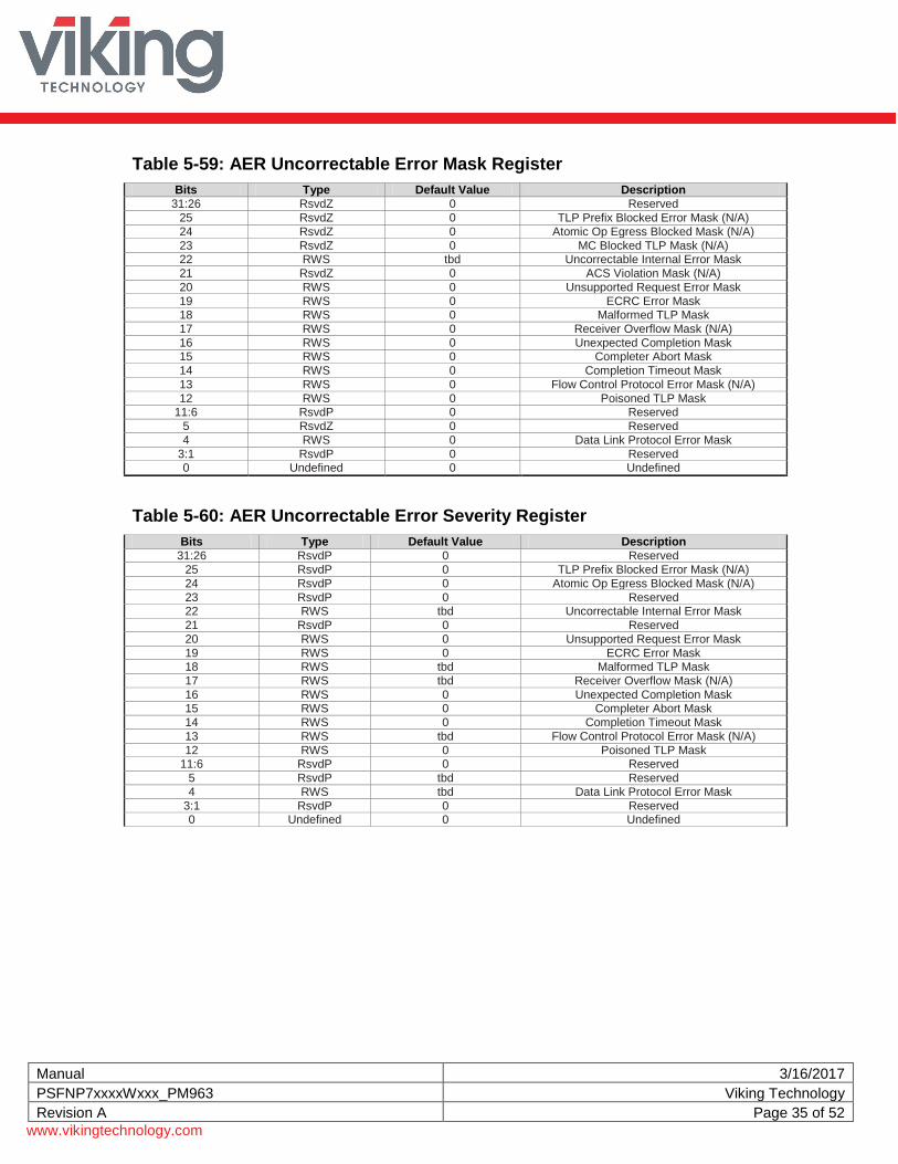
Table 5-59: AER Uncorrectable Error Mask Register
Bits Type Default Value Description
31:26 RsvdZ 0 Reserved
25 RsvdZ 0 TLP Prefix Blocked Error Mask (N/A)
24 RsvdZ 0 Atomic Op Egress Blocked Mask (N/A)
23 RsvdZ 0 MC Blocked TLP Mask (N/A) 22 RWS tbd Uncorrectable Internal Error Mask
21 RsvdZ 0 ACS Violation Mask (N/A)
20 RWS 0 Unsupported Request Error Mask
19 RWS 0 ECRC Error Mask 18 RWS 0 Malformed TLP Mask
17 RWS 0 Receiver Overflow Mask (N/A)
16 RWS 0 Unexpected Completion Mask 15 RWS 0 Completer Abort Mask
14 RWS 0 Completion Timeout Mask
13 RWS 0 Flow Control Protocol Error Mask (N/A)
12 RWS 0 Poisoned TLP Mask 11:6 RsvdP 0 Reserved
5 RsvdZ 0 Reserved
4 RWS 0 Data Link Protocol Error Mask
3:1 RsvdP 0 Reserved 0 Undefined 0 Undefined
Table 5-60: AER Uncorrectable Error Severity Register
Bits Type Default Value Description
31:26 RsvdP 0 Reserved
25 RsvdP 0 TLP Prefix Blocked Error Mask (N/A)
24 RsvdP 0 Atomic Op Egress Blocked Mask (N/A)
23 RsvdP 0 Reserved 22 RWS tbd Uncorrectable Internal Error Mask
21 RsvdP 0 Reserved
20 RWS 0 Unsupported Request Error Mask
19 RWS 0 ECRC Error Mask 18 RWS tbd Malformed TLP Mask
17 RWS tbd Receiver Overflow Mask (N/A)
16 RWS 0 Unexpected Completion Mask 15 RWS 0 Completer Abort Mask
14 RWS 0 Completion Timeout Mask
13 RWS tbd Flow Control Protocol Error Mask (N/A)
12 RWS 0 Poisoned TLP Mask 11:6 RsvdP 0 Reserved
5 RsvdP tbd Reserved
4 RWS tbd Data Link Protocol Error Mask
3:1 RsvdP 0 Reserved 0 Undefined 0 Undefined
Manual 3/16/2017
PSFNP7xxxxWxxx_PM963 Viking Technology
Revision A Page 36 of 52
www.vikingtechnology.com
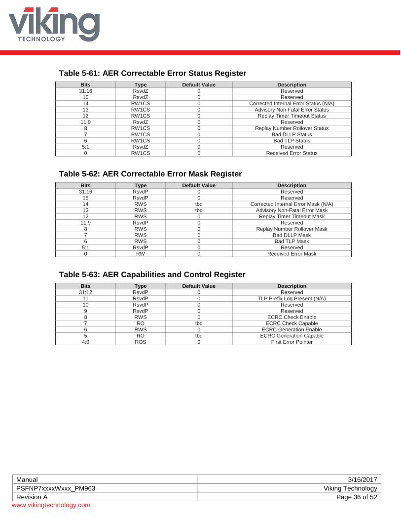
Table 5-61: AER Correctable Error Status Register
Bits Type Default Value Description
31:16 RsvdZ 0 Reserved
15 RsvdZ 0 Reserved
14 RW1CS 0 Corrected Internal Error Status (N/A)
13 RW1CS 0 Advisory Non-Fatal Error Status 12 RW1CS 0 Replay Timer Timeout Status
11:9 RsvdZ 0 Reserved
8 RW1CS 0 Replay Number Rollover Status
7 RW1CS 0 Bad DLLP Status 6 RW1CS 0 Bad TLP Status
5:1 RsvdZ 0 Reserved
0 RW1CS 0 Received Error Status
Table 5-62: AER Correctable Error Mask Register
Bits Type Default Value Description
31:16 RsvdP 0 Reserved
15 RsvdP 0 Reserved
14 RWS tbd Corrected Internal Error Mask (N/A)
13 RWS tbd Advisory Non-Fatal Error Mask 12 RWS 0 Replay Timer Timeout Mask
11:9 RsvdP 0 Reserved
8 RWS 0 Replay Number Rollover Mask 7 RWS 0 Bad DLLP Mask
6 RWS 0 Bad TLP Mask
5:1 RsvdP 0 Reserved
0 RW 0 Received Error Mask
Table 5-63: AER Capabilities and Control Register
Bits Type Default Value Description
31:12 RsvdP 0 Reserved
11 RsvdP 0 TLP Prefix Log Present (N/A)
10 RsvdP 0 Reserved
9 RsvdP 0 Reserved 8 RWS 0 ECRC Check Enable
7 RO tbd ECRC Check Capable
6 RWS 0 ECRC Generation Enable 5 RO tbd ECRC Generation Capable
4:0 ROS 0 First Error Pointer
Manual 3/16/2017
PSFNP7xxxxWxxx_PM963 Viking Technology
Revision A Page 37 of 52
www.vikingtechnology.com
Table 5-64: AER Header Log Register
Bits Type Default Value Description
0 ROS 0 Header Byte 3
1 ROS 0 Header Byte 2
2 ROS 0 Header Byte 1
3 ROS 0 Header Byte 0 4 ROS 0 Header Byte 7
5 ROS 0 Header Byte 6
6 ROS 0 Header Byte 5
7 ROS 0 Header Byte 4 8 ROS 0 Header Byte 11
9 ROS 0 Header Byte 10
10 ROS 0 Header Byte 9 11 ROS 0 Header Byte 8
12 ROS 0 Header Byte 15
13 ROS 0 Header Byte 14
14 ROS 0 Header Byte 13 15 ROS 0 Header Byte 12
Table 5-65: AER TLP Prefix Log Register
Bits Type Default Value Description
0 RO 0 First TLP Prefix Log Byte 3 (N/A)
1 RO 0 First TLP Prefix Log Byte 2 (N/A) 2 RO 0 First TLP Prefix Log Byte 1 (N/A)
3 RO 0 First TLP Prefix Log Byte 0 (N/A)
4 RO 0 Second TLP Prefix Log Byte 7 (N/A)
5 RO 0 Second TLP Prefix Log Byte 6 (N/A) 6 RO 0 Second TLP Prefix Log Byte 5 (N/A)
7 RO 0 Second TLP Prefix Log Byte 4 (N/A)
8 RO 0 Third TLP Prefix Log Byte 11 (N/A)
9 RO 0 Third TLP Prefix Log Byte 10 (N/A) 10 RO 0 Third TLP Prefix Log Byte 9 (N/A)
11 RO 0 Third TLP Prefix Log Byte 8 (N/A)
12 RO 0 Fourth TLP Prefix Log Byte 15 (N/A)
13 RO 0 Fourth TLP Prefix Log Byte 14 (N/A) 14 RO 0 Fourth TLP Prefix Log Byte 13 (N/A)
15 RO 0 Fourth TLP Prefix Log Byte 12 (N/A)
Table 5-66: Secondary PCI Express Capability Register Summary
Start Address End Address Symbol Description
168h 16Bh SPXID Secondary PCI Express Capability 16Ch 16Fh PXLC3 PCI Express Link Control 3
170h 173h PXLE PCI Express Lane Error Status
174h 175h PXL0EC PCI Express Lane 0 Equalization Control
176h 177h PXL1EC PCI Express Lane 1 Equalization Control 178h 179h PXL2EC PCI Express Lane 2 Equalization Control
17Ah 17Bh PXL3EC PCI Express Lane 3 Equalization Control
Table 5-67: Secondary PCI Express Capability ID Register
Bits Type Default Value Description
31:20 RO tbd Next Pointer (Viking Vendor Specific Capability) 19:16 RO tbd Capability Version
15:0 RO tbd Capability ID (Secondary PCI Express
Extended capability)
Manual 3/16/2017
PSFNP7xxxxWxxx_PM963 Viking Technology
Revision A Page 38 of 52
www.vikingtechnology.com
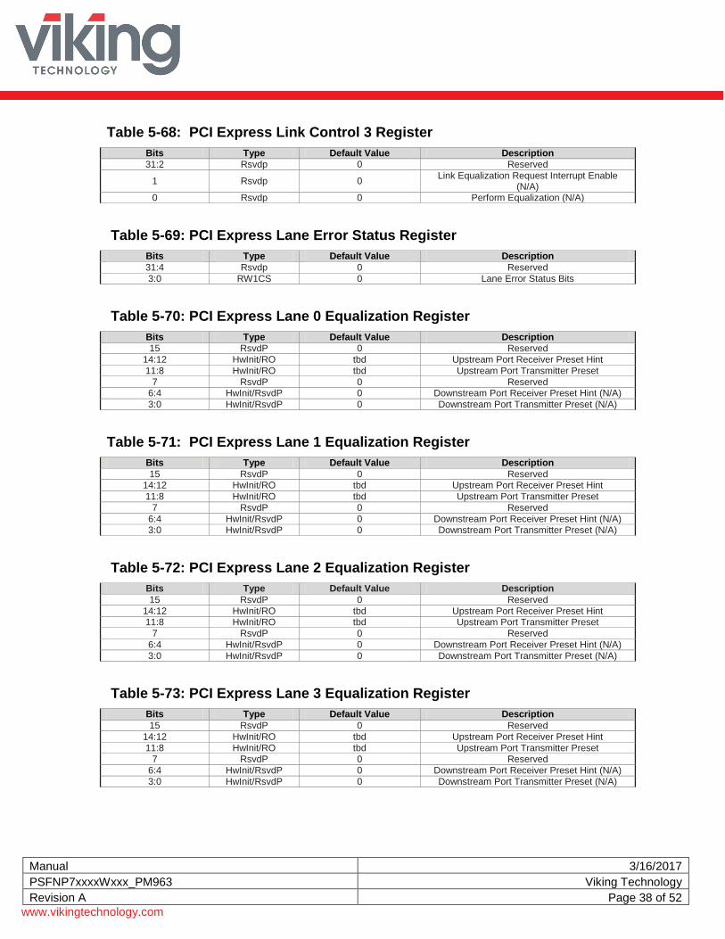
Table 5-68: PCI Express Link Control 3 Register
Bits Type Default Value Description
31:2 Rsvdp 0 Reserved
1 Rsvdp 0 Link Equalization Request Interrupt Enable
(N/A) 0 Rsvdp 0 Perform Equalization (N/A)
Table 5-69: PCI Express Lane Error Status Register
Bits Type Default Value Description
31:4 Rsvdp 0 Reserved
3:0 RW1CS 0 Lane Error Status Bits
Table 5-70: PCI Express Lane 0 Equalization Register
Bits Type Default Value Description
15 RsvdP 0 Reserved
14:12 HwInit/RO tbd Upstream Port Receiver Preset Hint
11:8 HwInit/RO tbd Upstream Port Transmitter Preset
7 RsvdP 0 Reserved 6:4 HwInit/RsvdP 0 Downstream Port Receiver Preset Hint (N/A)
3:0 HwInit/RsvdP 0 Downstream Port Transmitter Preset (N/A)
Table 5-71: PCI Express Lane 1 Equalization Register
Bits Type Default Value Description
15 RsvdP 0 Reserved 14:12 HwInit/RO tbd Upstream Port Receiver Preset Hint
11:8 HwInit/RO tbd Upstream Port Transmitter Preset
7 RsvdP 0 Reserved
6:4 HwInit/RsvdP 0 Downstream Port Receiver Preset Hint (N/A) 3:0 HwInit/RsvdP 0 Downstream Port Transmitter Preset (N/A)
Table 5-72: PCI Express Lane 2 Equalization Register
Bits Type Default Value Description
15 RsvdP 0 Reserved
14:12 HwInit/RO tbd Upstream Port Receiver Preset Hint 11:8 HwInit/RO tbd Upstream Port Transmitter Preset
7 RsvdP 0 Reserved
6:4 HwInit/RsvdP 0 Downstream Port Receiver Preset Hint (N/A)
3:0 HwInit/RsvdP 0 Downstream Port Transmitter Preset (N/A)
Table 5-73: PCI Express Lane 3 Equalization Register
Bits Type Default Value Description
15 RsvdP 0 Reserved
14:12 HwInit/RO tbd Upstream Port Receiver Preset Hint
11:8 HwInit/RO tbd Upstream Port Transmitter Preset 7 RsvdP 0 Reserved
6:4 HwInit/RsvdP 0 Downstream Port Receiver Preset Hint (N/A)
3:0 HwInit/RsvdP 0 Downstream Port Transmitter Preset (N/A)
Manual 3/16/2017
PSFNP7xxxxWxxx_PM963 Viking Technology
Revision A Page 39 of 52
www.vikingtechnology.com
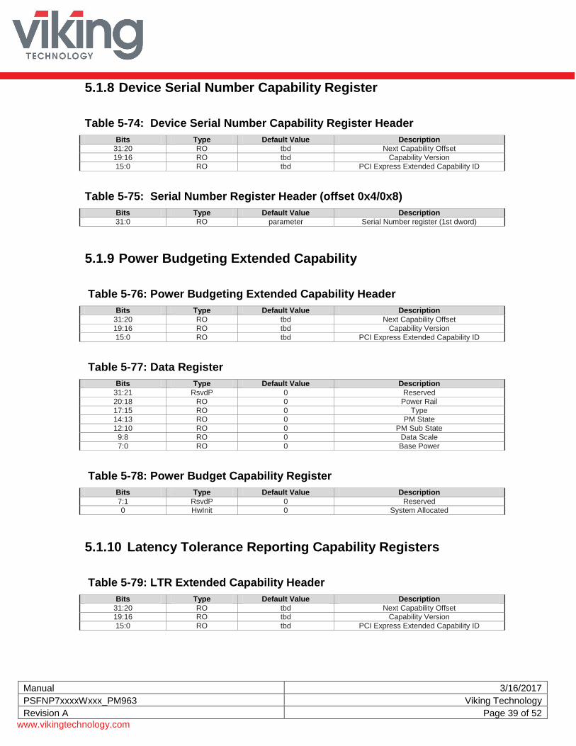
5.1.8 Device Serial Number Capability Register
Table 5-74: Device Serial Number Capability Register Header
Bits Type Default Value Description
31:20 RO tbd Next Capability Offset
19:16 RO tbd Capability Version
15:0 RO tbd PCI Express Extended Capability ID
Table 5-75: Serial Number Register Header (offset 0x4/0x8)
Bits Type Default Value Description
31:0 RO parameter Serial Number register (1st dword)
5.1.9 Power Budgeting Extended Capability
Table 5-76: Power Budgeting Extended Capability Header
Bits Type Default Value Description
31:20 RO tbd Next Capability Offset
19:16 RO tbd Capability Version
15:0 RO tbd PCI Express Extended Capability ID
Table 5-77: Data Register
Bits Type Default Value Description
31:21 RsvdP 0 Reserved
20:18 RO 0 Power Rail
17:15 RO 0 Type 14:13 RO 0 PM State
12:10 RO 0 PM Sub State
9:8 RO 0 Data Scale
7:0 RO 0 Base Power
Table 5-78: Power Budget Capability Register
Bits Type Default Value Description
7:1 RsvdP 0 Reserved
0 HwInit 0 System Allocated
5.1.10 Latency Tolerance Reporting Capability Registers
Table 5-79: LTR Extended Capability Header
Bits Type Default Value Description
31:20 RO tbd Next Capability Offset 19:16 RO tbd Capability Version
15:0 RO tbd PCI Express Extended Capability ID
Manual 3/16/2017
PSFNP7xxxxWxxx_PM963 Viking Technology
Revision A Page 40 of 52
www.vikingtechnology.com
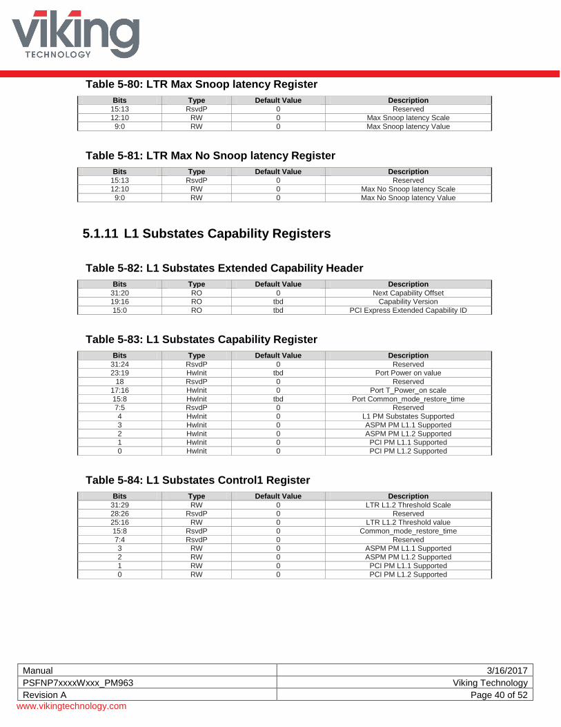
Table 5-80: LTR Max Snoop latency Register
Bits Type Default Value Description
15:13 RsvdP 0 Reserved
12:10 RW 0 Max Snoop latency Scale
9:0 RW 0 Max Snoop latency Value
Table 5-81: LTR Max No Snoop latency Register
Bits Type Default Value Description
15:13 RsvdP 0 Reserved
12:10 RW 0 Max No Snoop latency Scale
9:0 RW 0 Max No Snoop latency Value
5.1.11 L1 Substates Capability Registers
Table 5-82: L1 Substates Extended Capability Header
Bits Type Default Value Description
31:20 RO 0 Next Capability Offset 19:16 RO tbd Capability Version
15:0 RO tbd PCI Express Extended Capability ID
Table 5-83: L1 Substates Capability Register
Bits Type Default Value Description
31:24 RsvdP 0 Reserved 23:19 HwInit tbd Port Power on value
18 RsvdP 0 Reserved
17:16 HwInit 0 Port T_Power_on scale
15:8 HwInit tbd Port Common_mode_restore_time 7:5 RsvdP 0 Reserved
4 HwInit 0 L1 PM Substates Supported
3 HwInit 0 ASPM PM L1.1 Supported
2 HwInit 0 ASPM PM L1.2 Supported 1 HwInit 0 PCI PM L1.1 Supported
0 HwInit 0 PCI PM L1.2 Supported
Table 5-84: L1 Substates Control1 Register
Bits Type Default Value Description
31:29 RW 0 LTR L1.2 Threshold Scale 28:26 RsvdP 0 Reserved
25:16 RW 0 LTR L1.2 Threshold value
15:8 RsvdP 0 Common_mode_restore_time
7:4 RsvdP 0 Reserved 3 RW 0 ASPM PM L1.1 Supported
2 RW 0 ASPM PM L1.2 Supported
1 RW 0 PCI PM L1.1 Supported
0 RW 0 PCI PM L1.2 Supported
Manual 3/16/2017
PSFNP7xxxxWxxx_PM963 Viking Technology
Revision A Page 41 of 52
www.vikingtechnology.com
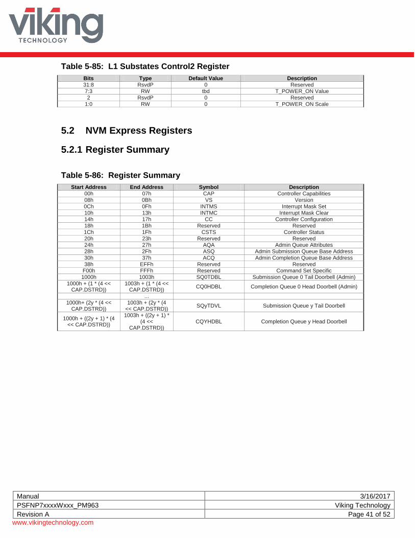
Table 5-85: L1 Substates Control2 Register
Bits Type Default Value Description
31:8 RsvdP 0 Reserved
7:3 RW tbd T_POWER_ON Value
2 RsvdP 0 Reserved
1:0 RW 0 T_POWER_ON Scale
5.2 NVM Express Registers
5.2.1 Register Summary
Table 5-86: Register Summary
Start Address End Address Symbol Description
00h 07h CAP Controller Capabilities
08h 0Bh VS Version
0Ch 0Fh INTMS Interrupt Mask Set
10h 13h INTMC Interrupt Mask Clear 14h 17h CC Controller Configuration
18h 1Bh Reserved Reserved
1Ch 1Fh CSTS Controller Status
20h 23h Reserved Reserved 24h 27h AQA Admin Queue Attributes
28h 2Fh ASQ Admin Submission Queue Base Address
30h 37h ACQ Admin Completion Queue Base Address
38h EFFh Reserved Reserved F00h FFFh Reserved Command Set Specific
1000h 1003h SQ0TDBL Submission Queue 0 Tail Doorbell (Admin)
1000h + (1 * (4 << CAP.DSTRD))
1003h + (1 * (4 << CAP.DSTRD))
CQ0HDBL Completion Queue 0 Head Doorbell (Admin)
...
1000h+ (2y * (4 << CAP.DSTRD))
1003h + (2y * (4 << CAP.DSTRD))
SQyTDVL Submission Queue y Tail Doorbell
1000h + ((2y + 1) * (4 << CAP.DSTRD))
1003h + ((2y + 1) * (4 <<
CAP.DSTRD)) CQYHDBL Completion Queue y Head Doorbell
Manual 3/16/2017
PSFNP7xxxxWxxx_PM963 Viking Technology
Revision A Page 42 of 52
www.vikingtechnology.com
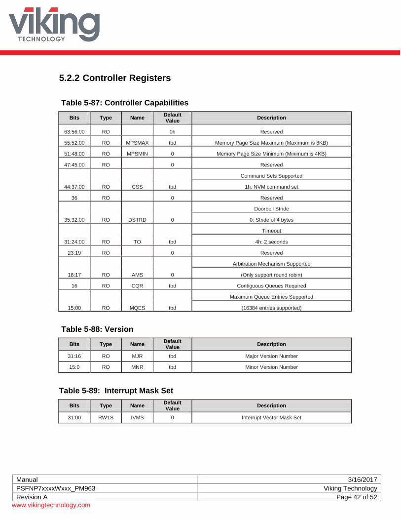
5.2.2 Controller Registers
Table 5-87: Controller Capabilities
Bits Type Name Default Value
Description
63:56:00 RO 0h Reserved
55:52:00 RO MPSMAX tbd Memory Page Size Maximum (Maximum is 8KB)
51:48:00 RO MPSMIN 0 Memory Page Size Minimum (Minimum is 4KB)
47:45:00 RO 0 Reserved
44:37:00 RO CSS tbd
Command Sets Supported
1h: NVM command set
36 RO 0 Reserved
35:32:00 RO DSTRD 0
Doorbell Stride
0: Stride of 4 bytes
31:24:00 RO TO tbd
Timeout
4h: 2 seconds
23:19 RO 0 Reserved
18:17 RO AMS 0
Arbitration Mechanism Supported
(Only support round robin)
16 RO CQR tbd Contiguous Queues Required
15:00 RO MQES tbd
Maximum Queue Entries Supported
(16384 entries supported)
Table 5-88: Version
Bits Type Name Default Value
Description
31:16 RO MJR tbd Major Version Number
15:0 RO MNR tbd Minor Version Number
Table 5-89: Interrupt Mask Set
Bits Type Name Default Value
Description
31:00 RW1S IVMS 0 Interrupt Vector Mask Set
Manual 3/16/2017
PSFNP7xxxxWxxx_PM963 Viking Technology
Revision A Page 43 of 52
www.vikingtechnology.com
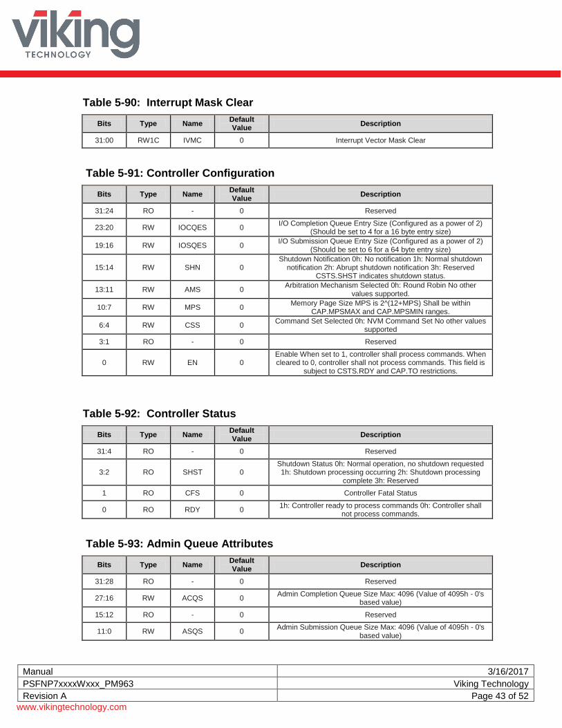
Table 5-90: Interrupt Mask Clear
Bits Type Name Default Value
Description
31:00 RW1C IVMC 0 Interrupt Vector Mask Clear
Table 5-91: Controller Configuration
Bits Type Name Default Value
Description
31:24 RO - 0 Reserved
23:20 RW IOCQES 0 I/O Completion Queue Entry Size (Configured as a power of 2)
(Should be set to 4 for a 16 byte entry size)
19:16 RW IOSQES 0 I/O Submission Queue Entry Size (Configured as a power of 2)
(Should be set to 6 for a 64 byte entry size)
15:14 RW SHN 0 Shutdown Notification 0h: No notification 1h: Normal shutdown
notification 2h: Abrupt shutdown notification 3h: Reserved CSTS.SHST indicates shutdown status.
13:11 RW AMS 0 Arbitration Mechanism Selected 0h: Round Robin No other
values supported.
10:7 RW MPS 0 Memory Page Size MPS is 2^(12+MPS) Shall be within
CAP.MPSMAX and CAP.MPSMIN ranges.
6:4 RW CSS 0 Command Set Selected 0h: NVM Command Set No other values
supported
3:1 RO - 0 Reserved
0 RW EN 0 Enable When set to 1, controller shall process commands. When cleared to 0, controller shall not process commands. This field is
subject to CSTS.RDY and CAP.TO restrictions.
Table 5-92: Controller Status
Bits Type Name Default Value
Description
31:4 RO - 0 Reserved
3:2 RO SHST 0 Shutdown Status 0h: Normal operation, no shutdown requested 1h: Shutdown processing occurring 2h: Shutdown processing
complete 3h: Reserved
1 RO CFS 0 Controller Fatal Status
0 RO RDY 0 1h: Controller ready to process commands 0h: Controller shall
not process commands.
Table 5-93: Admin Queue Attributes
Bits Type Name Default Value
Description
31:28 RO - 0 Reserved
27:16 RW ACQS 0 Admin Completion Queue Size Max: 4096 (Value of 4095h - 0's
based value)
15:12 RO - 0 Reserved
11:0 RW ASQS 0 Admin Submission Queue Size Max: 4096 (Value of 4095h - 0's
based value)
Manual 3/16/2017
PSFNP7xxxxWxxx_PM963 Viking Technology
Revision A Page 44 of 52
www.vikingtechnology.com
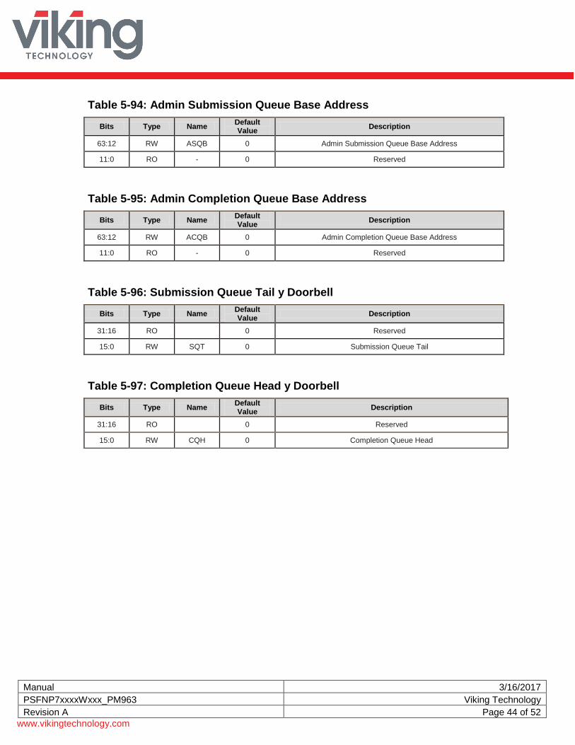
Table 5-94: Admin Submission Queue Base Address
Bits Type Name Default Value
Description
63:12 RW ASQB 0 Admin Submission Queue Base Address
11:0 RO - 0 Reserved
Table 5-95: Admin Completion Queue Base Address
Bits Type Name Default Value
Description
63:12 RW ACQB 0 Admin Completion Queue Base Address
11:0 RO - 0 Reserved
Table 5-96: Submission Queue Tail y Doorbell
Bits Type Name Default Value
Description
31:16 RO
0 Reserved
15:0 RW SQT 0 Submission Queue Tail
Table 5-97: Completion Queue Head y Doorbell
Bits Type Name Default Value
Description
31:16 RO
0 Reserved
15:0 RW CQH 0 Completion Queue Head
Manual 3/16/2017
PSFNP7xxxxWxxx_PM963 Viking Technology
Revision A Page 45 of 52
www.vikingtechnology.com
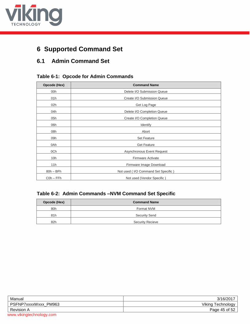
6 Supported Command Set
6.1 Admin Command Set
Table 6-1: Opcode for Admin Commands
Opcode (Hex) Command Name
00h Delete I/O Submission Queue
01h Create I/O Submission Queue
02h Get Log Page
04h Delete I/O Completion Queue
05h Create I/O Completion Queue
06h Identify
08h Abort
09h Set Feature
0Ah Get Feature
0Ch Asynchronous Event Request
10h Firmware Activate
11h Firmware Image Download
80h – BFh Not used ( I/O Command Set Specific )
C0h – FFh Not used (Vendor Specific )
Table 6-2: Admin Commands –NVM Command Set Specific
Opcode (Hex) Command Name
80h Format NVM
81h Security Send
82h Security Recieve
Manual 3/16/2017
PSFNP7xxxxWxxx_PM963 Viking Technology
Revision A Page 46 of 52
www.vikingtechnology.com
6.1.1 Identify Command
Table 6-3: Identify Controller Data Structure
Bytes O/M Default Value Description
1:00 M tbd PCI Vendor ID
3:02 M tbd PCI Subsystem Vendor ID
23:04 M tbd Serial Number (ASCII), #:Variables
63:24:00 M (see Viking PN table) Model Number (ASCII)
71:64 M tbd Firmware Revision, #:Variables
72 M tbd Recommended Arbitration Burst
75:73 M tbd IEEE OUI
76 O tbd
Controller Multi-Path I/O and Namespace Sharing Bit 2: 1h - Controller is associated with an SR-IOV Virtual Function 0h - Controller is associated with a PCI Function. Bit 1: 1h -
Device has Two or More controller 0h - Device has One Controller Bit 0: 1h - Device has Two or More physical PCI Express ports 0h - Device
has One PCI Express port
77 M tbd
Maximum Data Transfer Size Bit 0: 1h - Supported (dual port – future value) 0h - Not
Support (Single Port) Maximum Data Transfer Size (MDTS)
79:78 M tbd Controller ID (CNTLID)
255:80
tbd Reserved
257:256 M tbd
Optional Admin Command Support Bits 15:3 - Reserved Bit 3: 1h - Namespace Management
and Namespace Attachment Commands Supported (PM953 conditionally supports the Namespace Management and Namespace
Attachment command(NVMe v1.2 specification) for reconfigurable overprovisioning) Bit 2: 1h – Firmware Activate/Download Supported Bit 1: 1h Format NVM Supported Bit 0: 0 Security Send and Security Receive Not Supported
258 M tbd Abort Command Limit (Maximum number of
concurrently outstanding Abort commands) (0's based value)
259 M tbd
Asynchronous Event Request Limit (Maximum number of concurrently outstanding
Asynchronous Event Request commands) (0's based value)
260 M tbd Firmware Updates Bits 7:4 – Reserved Bits 3:1 – Number of firmware slots Bit 0 – 1h Slot 1 is
read only
261 M tbd Log Page Attributes Bits 7:1 – Reserved Bit 0: 0h SMART data is global for all namespaces
262 M tbd Error Log Page Entries (Number of Error
Information log entries stored by controller) (0's based value)
Manual 3/16/2017
PSFNP7xxxxWxxx_PM963 Viking Technology
Revision A Page 47 of 52
www.vikingtechnology.com
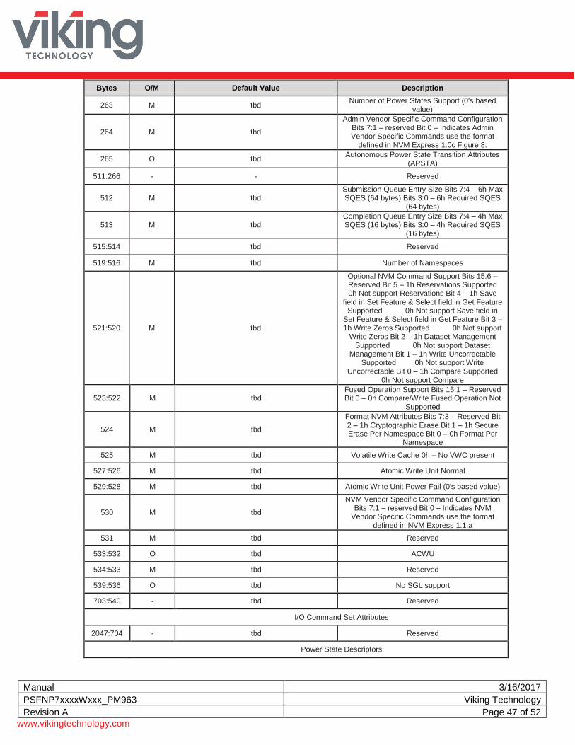
Bytes O/M Default Value Description
263 M tbd Number of Power States Support (0's based
value)
264 M tbd
Admin Vendor Specific Command Configuration Bits 7:1 – reserved Bit 0 – Indicates Admin Vendor Specific Commands use the format
defined in NVM Express 1.0c Figure 8.
265 O tbd Autonomous Power State Transition Attributes
(APSTA)
511:266 - - Reserved
512 M tbd Submission Queue Entry Size Bits 7:4 – 6h Max SQES (64 bytes) Bits 3:0 – 6h Required SQES
(64 bytes)
513 M tbd Completion Queue Entry Size Bits 7:4 – 4h Max SQES (16 bytes) Bits 3:0 – 4h Required SQES
(16 bytes)
515:514
tbd Reserved
519:516 M tbd Number of Namespaces
521:520 M tbd
Optional NVM Command Support Bits 15:6 – Reserved Bit 5 – 1h Reservations Supported 0h Not support Reservations Bit 4 – 1h Save
field in Set Feature & Select field in Get Feature Supported 0h Not support Save field in
Set Feature & Select field in Get Feature Bit 3 – 1h Write Zeros Supported 0h Not support
Write Zeros Bit 2 – 1h Dataset Management Supported 0h Not support Dataset
Management Bit 1 – 1h Write Uncorrectable Supported 0h Not support Write
Uncorrectable Bit 0 – 1h Compare Supported 0h Not support Compare
523:522 M tbd Fused Operation Support Bits 15:1 – Reserved Bit 0 – 0h Compare/Write Fused Operation Not
Supported
524 M tbd
Format NVM Attributes Bits 7:3 – Reserved Bit 2 – 1h Cryptographic Erase Bit 1 – 1h Secure Erase Per Namespace Bit 0 – 0h Format Per
Namespace
525 M tbd Volatile Write Cache 0h – No VWC present
527:526 M tbd Atomic Write Unit Normal
529:528 M tbd Atomic Write Unit Power Fail (0's based value)
530 M tbd
NVM Vendor Specific Command Configuration Bits 7:1 – reserved Bit 0 – Indicates NVM
Vendor Specific Commands use the format defined in NVM Express 1.1.a
531 M tbd Reserved
533:532 O tbd ACWU
534:533 M tbd Reserved
539:536 O tbd No SGL support
703:540 - tbd Reserved
I/O Command Set Attributes
2047:704 - tbd Reserved
Power State Descriptors
Manual 3/16/2017
PSFNP7xxxxWxxx_PM963 Viking Technology
Revision A Page 48 of 52
www.vikingtechnology.com
Bytes O/M Default Value Description
2079:2048 M refer to 'Identify Power State Descriptor Data
Structure' Power State 0 Descriptor
2111:2080 O tbd N/A
2143:2112 O tbd N/A
... - tbd N/A
3071:3040 O tbd Power State 31 Descriptor (N/A)
Vendor Specific
4095:3072 - - Viking Reserved
Table 6-4: Identify Power State Descriptor Data Structure
Bits Power State 0
Description
255:125 0h Reserved
124:120 0h Relative Write Latency
119:117 0h Reserved
116:112 0h RelativeWriteThroughput
111:109 0h Reserved
108:104 0h RelativeReadLatency
103:101 0h Reserved
100:96 0h RelativeReadThroughput
95:64 5h Exit Latency
63:32:00 5h (QWU\/DWHQF\ ____XV__
31:26:00 0h Reserved
25 0h Non-Operational State
24 0h Max Power Scale
23:16 0h Reserved
15:00 384h Maximum Power
Manual 3/16/2017
PSFNP7xxxxWxxx_PM963 Viking Technology
Revision A Page 49 of 52
www.vikingtechnology.com
Table 6-5: Identify Namespace Data Structure
Bytes O/M Default Value Description
7:00 M tbd Namespace Size
15:88 M
120 240 480
Byte[7:0] DF94BB0h 1BF244B0h 37E436B0h
Namespace Capacity
23:16 M - Namespace Utilization A device may report Namespace
Utilization equal to Namespace Capacity at all times if the product is not targeted for thin provisioning environments
24 M tbd Namespace Features Bits 7:1 Reserved Bit 0: Thin
provisioning not supported
25 M tbd Number of LBA Formats
26 M tbd Formatted LBA Size Bits 7:5 – Reserved Bit 4: Metadata interleaved or separate (based on LBA format) Bit 3:0 –
Indicates LBA format
27 M tbd Metadata Capabilities Bits 7:2 – Reserved Bit 1 – Supports Metadata as separate buffer Bit 0 – Supports Metadata as
extended LBA
28 M tbd
End-to-end Data Protection Capabilities Bits 7:5 – Reserved Bit 4 – Supports protection information as last 8 bytes of Metadata Bit 3 – Supports protection information
as first 8 bytes of metadata Bit 2 – Supports Type 3 protection information Bit 1 – Supports Type 2 protection
information Bit 0 – Supports Type 1 protection information
29 M tbd
End-to-End Data Protection Type Settings Bits 7:4 – Reserved Bit 3 – 1: Protection information transferred as first 8 bytes of metadata Bit 3 – 0: Protection information transferred as last 8 bytes of metadata Bit 2:0 – 000b: Protection information disabled Bit 2:0 – 1h: Protection
type 1 enabled Bit 2:0 – 2h: Protection type 2 enabled Bit 2:0 – 3h: Protection type 3 enabled
30 O tbd
Namespace Multi-path I/O and Namespace sharing Capabilities (NMIC) Bits 7:1 - Reserved Bit 0 - 1 :
Accessible by two or more controllers Bit 0 - 0 : Private namespace
31 O
tbd
Reservation Capabilities (RESCAP) Bits 7 - Reserved Bits 6 - 1: Namespace supports the Exclusive Access (All Registrants reservation type) Bit 5 - 1 : Namespace
supports the Write Exclusive (All Registrants reservation type) Bit 4 - 1 : Namespace supports the Exclusive Access (Registrants only reservation type) Bit 3 - 1 : Namespace supports the Write Exclusive (Registrants only reservation type) Bit 2 - 1 : Namespace supports the Exclusive Access Reservation type Bit 1 - 1 : Namespace supports the Write Exclusive Reservation type Bit 0 - 1 : Namespace supports
the Persist Through Power Loss capability
119:32 -
tbd Reserved
127:120 M tbd IEEE Extended Unique Identifier(EUI64) #:Variables
131:128 M refer to 'LBA Format 0 Data Structure' LBA Format 0 Support
135:132 O tbd LBA Format 1 Support
Manual 3/16/2017
PSFNP7xxxxWxxx_PM963 Viking Technology
Revision A Page 50 of 52
www.vikingtechnology.com
Bytes O/M Default Value Description
139:136 O tbd LBA Format 2 Support
143:140 O tbd LBA Format 3 Support
147:144 O tbd LBA Format 4 Support (N/A)
…
191:188 O tbd LBA Format 15 Support (N/A)
383:192 -
tbd Reserved
Vendor Specific
4095:384 -
Viking Reserved
Table 6-6: LBA Format 0 Data Structure
Bits Name Default Value
Description
31:26:00
0 Reserved
25:24:00 RP 0 Relative Performance
23:16 LBADS tbd LBA Data Size
15:00 MS 0 Metadata Size
6.2 NVM Express I/O Command Set
Table 6-7: Opcode for NVM Express I/O Commands
Opcode (Hex) Command Name
00h Flush
01h Write
02h Read
04h Write Uncorrectable
05h Compare
08h Write Zeroes
09h Dataset Management
Manual 3/16/2017
PSFNP7xxxxWxxx_PM963 Viking Technology
Revision A Page 51 of 52
www.vikingtechnology.com
6.3 SMART/Health Information
Table 6-8: SMART/Health Information Log
Bytes Default Value Attribute Description
0 0
Critical Warning Bit 7:5 – Reserved Bit 4 – 1h: the available spare space has fallen below the threshold Bit 3 – 1h: the temperature has exceeded a critical threshold Bit 2 – 1h: the device reliability has been degraded due to significant media related errors or any internal
error that degrades device reliability Bit 1 – 1h: the media has been placed in read only mode Bit 0 – 1h: the volatile memory backup device has failed. (only valid if the controller
has a volatile memory backup solution)
2:01 current temp Temperature
3 tbd Available Spare
4 tbd Available Spare Threshold
5 0 Percentage Used
31:06:00 - Reserved
47:32:00 0 Data Units Read
63:48:00 0 Data Units Written
79:64 0 Host Read Commands
95:80 0 Host Write Commands
111:96 0 Controller Busy Time
127:112 0 Power Cycles
143:128 0 Power On Hours
159:144 0 8QVDIH_6KXWGRZQV
175:160 0 Media Errors
191:176 0 Number of Error Information Log Entries
Manual 3/16/2017
PSFNP7xxxxWxxx_PM963 Viking Technology
Revision A Page 52 of 52
www.vikingtechnology.com
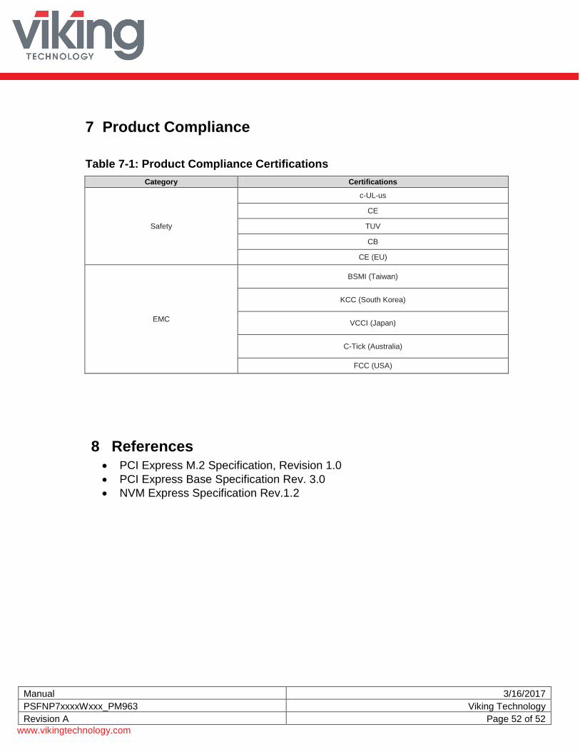
7 Product Compliance
Table 7-1: Product Compliance Certifications
Category Certifications
Safety
c-UL-us
CE
TUV
CB
CE (EU)
EMC
BSMI (Taiwan)
KCC (South Korea)
VCCI (Japan)
C-Tick (Australia)
FCC (USA)
8 References PCI Express M.2 Specification, Revision 1.0
PCI Express Base Specification Rev. 3.0
NVM Express Specification Rev.1.2