Embed Size (px)
Citation preview

SEEDLESS AND CATALYST- FREE GROWTH OF ZINC OXIDE
NANOSTRUCTURES ON GRAPHENE BY THERMAL EVAPORATION
NURUL FARIHA AHMAD
UNIVERSITI TEKNOLOGI MALAYSIA

SEEDLESS AND CATALYST-FREE GROWTH OF ZINC OXIDE
NANOSTRUCTURES ON GRAPHENE BY THERMAL EVAPORATION
NURUL FARIHA AHMAD
A thesis submitted in fulfillment of the
requirements for the award of the degree of
Master of Philosophy
Malaysia-Japan International
Institute of Technology
Universiti Teknologi Malaysia
MAY 2015

iii
To my beloved late father and mother,
Ahmad Mohd Noor
Bariah Mat Ali
My lovely siblings,
Salwa Ahmad
Busra Ahmad
Nurul Farhana Ahmad
Najiha Ahmad
Suhaidal Ismail

iv
ACKNOWLEDGEMNET
Alhamdulillah, thanks to Allah S.W.T the most merciful and the most
compassionate for the guidance and knowledge bestowed upon me, for without it I
would not have been able to come this far. Peace is upon him, Muhammad the
messenger of God.
Throughout the time I spent at Advanced Devices and Materials Engineering
(ADME) ikohza, Malaysia-Japan International Institute of Technology (MJIIT),
Universiti Teknologi Malaysia, there have been many people who have helped me in
this challenging work. It is a pleasure to thank a few of them here and there is no other
word to describe how grateful I am to the following individuals.
The most important influence on the succesful completion of this work was my
supervisor, Assoc. Prof. Ir. Dr. Abdul Manaf Hashim. He has had greatest influence on
my development as a researcher. He is an amazing researcher and mentor. He pushed me
to develop my weakness and exploit my strengths. His courage to tackle new and
difficult problems and withstand the many failures that accompany such risks is
admirable. His energy and excitement in research never seem to end. This work could
not possibly be done without his valuable advices and guidance.
I would like to thank Assoc. Prof. Dr. Mohamad Rusop Mahmood from the
Faculty of Electrical Engineering, Universiti Teknologi MARA for his willingness to co-
supervise my research and provides the platform for characterization equipments and
informative guidance for my development as a researcher. I would like to express my
special thanks to Prof. Dr. Kanji Yasui from Department of Electrical Engineering,
Nagaoka University of Technology, Japan for his stimulating and helpful discussions in
this work, contributing me with ideas and proving information as well as advices to
v
make this work more completed. Without their support and input, this thesis would have
not completed.
For the work in this thesis, I would like to thank all staffs and technicians of
MIMOS Berhad (Mr. Firdaus Mansor, Mr. Firdaus Abdullah, Mrs. Asma Atoh, Mrs.
Nor Aishah,), NANO-SciTech Centre, Universiti Teknologi MARA (Mrs. Nurul Wahida
Aziz), School of Materials and Mineral Resources Engineering, Universiti Sains
Malaysia (Mr Zaini Shaari) for their kind assistance during characterization process.
Besides that, thanks to MJIIT-UTM staffs (Mrs. Aishah Latif, Mrs Noridah Borhan, Ms
Fatin) for their kind assistance during my master degree administration process. I also
would like to thank the members of Yasui Laboratory, Nagaoka University of
Technology ( Mr. Yasuhiro Tamayama, Mr. Yuki ohashi, Mr. Tomoki Nakamura, Mr.
Tomohiko Takeuchi, Mr. Yusuke Teraguchi, Mr. Naoya Yamaguchi and Mr. Kazuki
Takezawa) for supporting me during my three months internship there. They are willing
to share knowledge and guide me especially in operating the equipment and data
interpretation process.
One of the wonderful aspects of doing research is going through it together with
other research members. I was lucky enough to work with phenomenal batch in ADME
Ikohza. I would like to express my gratitude to my colleagues: Dr. Mastura Shafinaz
Zainal Abidin, Dr. Farahiyah Mustafa, Mrs. Nurul Izni Rusli, Dr. Shaharin Fadzli Abd.
Rahman, Dr. Budi Astuti Sangadji, Ms. Nur suhaili Abdul Aziz, Ms. Nurul Azzyaty
Jayah, Ms. Norizzawati Mohd. Ghazali, Ms. Nur Hamizah Zainal Ariffin, Ms. Nur
Ashikyn Hambali, Mrs. Freddawati Rasshidy Wong, Mr. Desrino Jalani, Mr. Tahsin
Morshed, Mr. Amgad Ahmed Ali and Mr. Sarwan Sanif for their ingenious ideas during
our discussions and great support throughtout the studies. Also, thank you to Ms. Siti
Sarah Mohd Azlan, Mrs. Noorradiyah Ismail, Mr. Mohamad Arif Rahim, Ms. Siti Nur
Murni Mazli, Ms. Nur Atikah Shaari, Ms. Syahirah Muzi and Ms. Nurul Farah Ayuni
Mohd Zu, Ms. Aida den and Ms. Norani Manaf for their friendship and assistance.
I want to give my special heartfelt thanks to my family who I owe so much, my
late father Mr Ahmad Mohd Noor and my supportive mother Mrs. Bariah Mat Ali for
the tremendous and endless support. It is their love and support through the years that

vi
brought me to here and their love for family and each other continues to inspire me this
day. Also, my siblings, Salwa Ahmad, Suhaidal Ismail, Busra Ahmad, Nurul Farhana
Ahmad and Najiha Ahmad. Thank you for shaping my life while growing up and as we
go through life, all of you are always continue to be in my thoughts. Their endless love
is the priceless treasure that gives me light to overcome the darkness. Thank you for
always stay by my side.
This work has been funded by the Malaysia-Japan International Institute of
Technology, the Universiti Teknologi Malaysia, the Ministry of Higher Education, the
Ministry of Science Technology and Innovation, the Hitachi Foundation and the Nippon
Sheet Glass Corporation. This work could not possibly be done without these funding.
vii
ABSTRACT
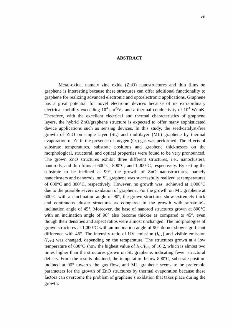
Metal-oxide, namely zinc oxide (ZnO) nanostructures and thin films on
graphene is interesting because these structures can offer additional functionality to
graphene for realizing advanced electronic and optoelectronic applications. Graphene
has a great potential for novel electronic devices because of its extraordinary
electrical mobility exceeding 104 cm
2/Vs and a thermal conductivity of 10
3 W/mK.
Therefore, with the excellent electrical and thermal characteristics of graphene
layers, the hybrid ZnO/graphene structure is expected to offer many sophisticated
device applications such as sensing devices. In this study, the seed/catalyst-free
growth of ZnO on single layer (SL) and multilayer (ML) graphene by thermal
evaporation of Zn in the presence of oxygen (O2) gas was performed. The effects of
substrate temperatures, substrate positions and graphene thicknesses on the
morphological, structural, and optical properties were found to be very pronounced.
The grown ZnO structures exhibit three different structures, i.e., nanoclusters,
nanorods, and thin films at 600°C, 800°C, and 1,000°C, respectively. By setting the
substrate to be inclined at 90°, the growth of ZnO nanostructures, namely
nanoclusters and nanorods, on SL graphene was successfully realized at temperatures
of 600°C and 800°C, respectively. However, no growth was achieved at 1,000°C
due to the possible severe oxidation of graphene. For the growth on ML graphene at
600°C with an inclination angle of 90°, the grown structures show extremely thick
and continuous cluster structures as compared to the growth with substrate’s
inclination angle of 45°. Moreover, the base of nanorod structures grown at 800°C
with an inclination angle of 90° also become thicker as compared to 45°, even
though their densities and aspect ratios were almost unchanged. The morphologies of
grown structures at 1,000°C with an inclination angle of 90° do not show significant
difference with 45°. The intensity ratio of UV emission (IUV) and visible emission
(IVIS) was changed, depending on the temperature. The structures grown at a low
temperature of 600°C show the highest value of IUV/IVIS of 16.2, which is almost two
times higher than the structures grown on SL graphene, indicating fewer structural
defects. From the results obtained, the temperature below 800°C, substrate position
inclined at 90° towards the gas flow, and ML graphene seems to be preferable
parameters for the growth of ZnO structures by thermal evaporation because these
factors can overcome the problem of graphene’s oxidation that takes place during the
growth.

viii
ABSTRAK
Logam-oksida, iaitu zink oksida (ZnO) berstruktur nano dan filem nipis di
atas grafin amat menarik kerana ia boleh menawarkan fungsi tambahan kepada grafin
untuk merealisasikan aplikasi elektronik dan optoelektronik maju. Grafin mempunyai
potensi besar untuk peranti elektronik novel kerana mobiliti elektrik yang luar biasa
melebihi 104 cm
2/Vs dan kekonduksian terma 10
3 W/mK. Oleh itu, dengan ciri-ciri
elektrik dan haba yang sangat baik dari lapisan grafin, struktur hibrid ZnO/grafin
dijangka menawarkan banyak aplikasi peranti canggih. Dalam kajian ini,
pertumbuhan ZnO bebas pemangkin/benih di atas grafin berlapisan tunggal (SL) dan
lapisan berganda (ML) menggunakan penyejatan haba Zn dalam kehadiran oksigen
(O2) gas telah dilakukan. Kesan suhu substrat, kedudukan dan ketebalan substrat
grafin pada sifat-sifat morfologi, struktur, dan optik didapati sangat ketara. Pada
dasarnya, struktur ZnO yang tumbuh menunjukkan tiga struktur berbeza, iaitu
nanokluster, nanorod, dan filem nipis masing-masing pada 600°C, 800°C, dan
1,000°C. Dengan menetapkan substrat condong pada 90°, pertumbuhan struktur-
struktur nano ZnO iaitu nanokluster dan nanorod pada SL grafin telah berjaya
direalisasikan pada suhu 600°C dan 800°C. Walau bagaimanapun, tiada pertumbuhan
dicapai pada 1,000°C berkemungkinan akibat daripada pengoksidaan grafin yang
teruk. Untuk pertumbuhan di atas ML grafin pada 600°C dengan sudut kecondongan
90°, pertumbuhan menunjukkan struktur kelompok yang sangat tebal dan berterusan
berbanding dengan pertumbuhan pada sudut kecondongan substrat 45°. Selain itu,
tapak struktur nanorod yang tumbuh pada 800°C dengan sudut kecondongan 90°
juga menjadi lebih tebal berbanding 45°, walaupun kepadatan dan nisbah aspek
hampir tidak berubah. Struktur morfologi pada 1,000°C dengan sudut kecondongan
90° tidak menunjukkan perbezaan yang signifikan berbanding 45°. Nisbah keamatan
UV (IUV) dan sinar nampak (IVIS) berubah bergantung kepada suhu. Struktur yang
tumbuh pada suhu rendah daripada 600°C menunjukkan nilai tertinggi IUV / IVIS iaitu
16.2, yang hampir dua kali lebih tinggi daripada struktur yang tumbuh di atas SL
grafin, menunjukkan sedikit kecacatan struktur. Daripada keputusan yang diperolehi,
dapat disimpulkan bahawa suhu di bawah 800°C, kedudukan substrat condong pada
90 ° arah aliran gas, dan ML grafin seolah-olah menjadi parameter terbaik untuk
pertumbuhan struktur ZnO oleh penyejatan haba kerana faktor-faktor ini boleh
digunakan untuk mengatasi masalah pengoksidaan grafin yang berlaku semasa
pertumbuhan.

ix
TABLE OF CONTENTS
CHAPTER TITLE PAGE
DECLARATION ii
DEDICATION iii
ACKNOWLEDGEMENT iv
ABSTRACT vii
ABSTRAK viii
TABLE OF CONTENT ix
LIST OF TABLES xii
LIST OF FIGURES xiii
LIST OF ABBREVIATIONS xvi
LIST OF SYMBOLS xviii
LIST OF APPENDICES
xx
1 INTRODUCTION 1
1.1 Research Background
1.2 Research Motivation
1.3 Research Objectives
1.4 Research Activities
1.5 Thesis Organization
1
2
4
4
5

x
2 MATERIAL PROPERTIES OF ZINC OXIDE AND
GRAPHENE
7
2.1 Introduction
2.2 Material Properties of ZnO
2.2.1 Crystal and Surface Structure of ZnO
2.2.2 Basic Physical Parameters of ZnO
2.2.3 Electrical Properties of ZnO
2.2.4 Optical Properties of ZnO
2.3 Material Properties of graphene
2.3.1 Structural properties of Graphene
2.3.2 Hybrid Integration of ZnO/Graphene and
its Potential Application
2.4 Thermal Evaporation Growth of ZnO
nanostructures
2.5 Summary
7
7
8
10
11
13
13
15
16
18
19
3 THERMAL EVAPORATION SETUP AND
CHARACTERIZATION TECHNIQUES
21
3.1 Introduction
3.2 Properties of Substrate
3.3 Growth of ZnO by Thermal Evaporation
3.3.1 Growth Parameter
3.4 Analysis of samples
3.4.1 Field Emission Scanning Electron
Microscopy (FESEM) and Energy
Dispersive X-ray Specstroscopy (EDS)
3.4.2 X-ray Diffraction (XRD)
3.4.3 Photoluminescence (PL) Spectroscopy
3.5 Summary
21
21
24
25
27
27
29
30
30

xi
4 SYNTHESIS OF ZINC OXIDE NANOSTRUCTURES
ON GRAPHENE BY THERMAL EVAPORATION
32
4.1 Introduction
4.2 Effect of Oxygen Flow rate
4.3 Effect of substrate temperatures
4.3.1 Possible growth mechanism
4.4 Effect of Substrate Inclination Angle and graphene
thicknesses
4.4.1 Possible growth mechansim
4.5 Summary
32
32
35
42
44
52
54
5 CONCLUSION AND FUTURE WORK
5.1 Contribution of Present Work
5.2 Directions of Future Work
5.3 Summary
55
56
57
REFERRENCES 58
APPENDIX 70
xii
LIST OF TABLES
TABLE TITLE
PAGE
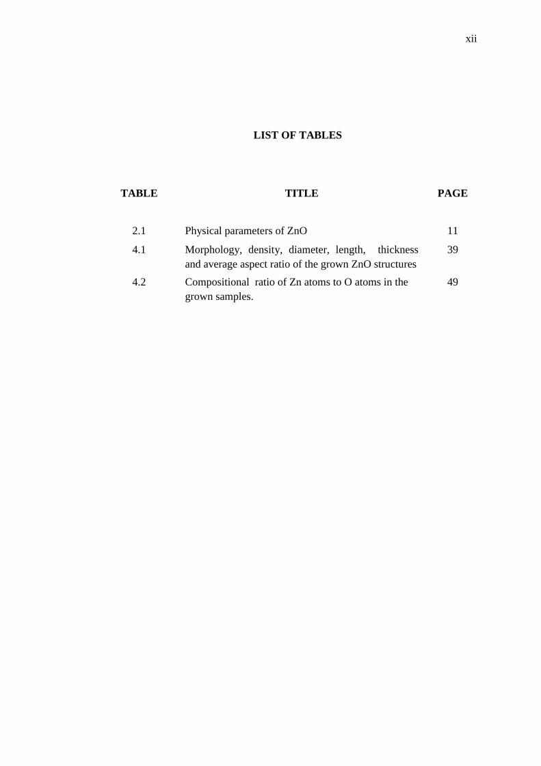
2.1 Physical parameters of ZnO 11
4.1 Morphology, density, diameter, length, thickness
and average aspect ratio of the grown ZnO structures
39
4.2
Compositional ratio of Zn atoms to O atoms in the
grown samples.
49

xii
LIST OF FIGURES
FIGURE NO. TITLE
PAGE
1.1 Evolution of Si-based nano electronics [36]
2
1.2 Research Activities
5
2.1 The wurtzite structure model of ZnO [39]
9
2.2 The rocksalt (left) and zincblende structure of ZnO
(right) [54]
9
2.3 Types of carbon allotrope (a) graphite (b) graphene (c)
fullerenes (d) carbon nanotubes [62]
14
2.4 Honeycomb lattice, the vectors 1 2 δ ,δ and 3 δ connect
nn carbon atoms, separated by a distance a = 0.142
nm. The vectors a1 and a2 are basis vectors of the
triangular Bravais lattice [68].
15
2.5 Schematic of the graphene structure (a) zigzag edge
and (b) armchair edge
16
3.1 FESEM images of graphene a) single layer b)
multilayer
22
3.2 (a) Raman spectra for as-received SL graphene (b)
Nomarski image of ML graphene, (c) Raman spectra
for as- received ML graphene (the measured regions
were identified in the circles)
23
3.3 Schematic of thermal evaporation setup
25
3.4
Time chart for ZnO nanostructures growth process 25
3.5
Schematic of FESEM-EDS 28
3.6
Bragg’s reflection of X-rays from two planes of atom
in a crystal solid
29
xiv
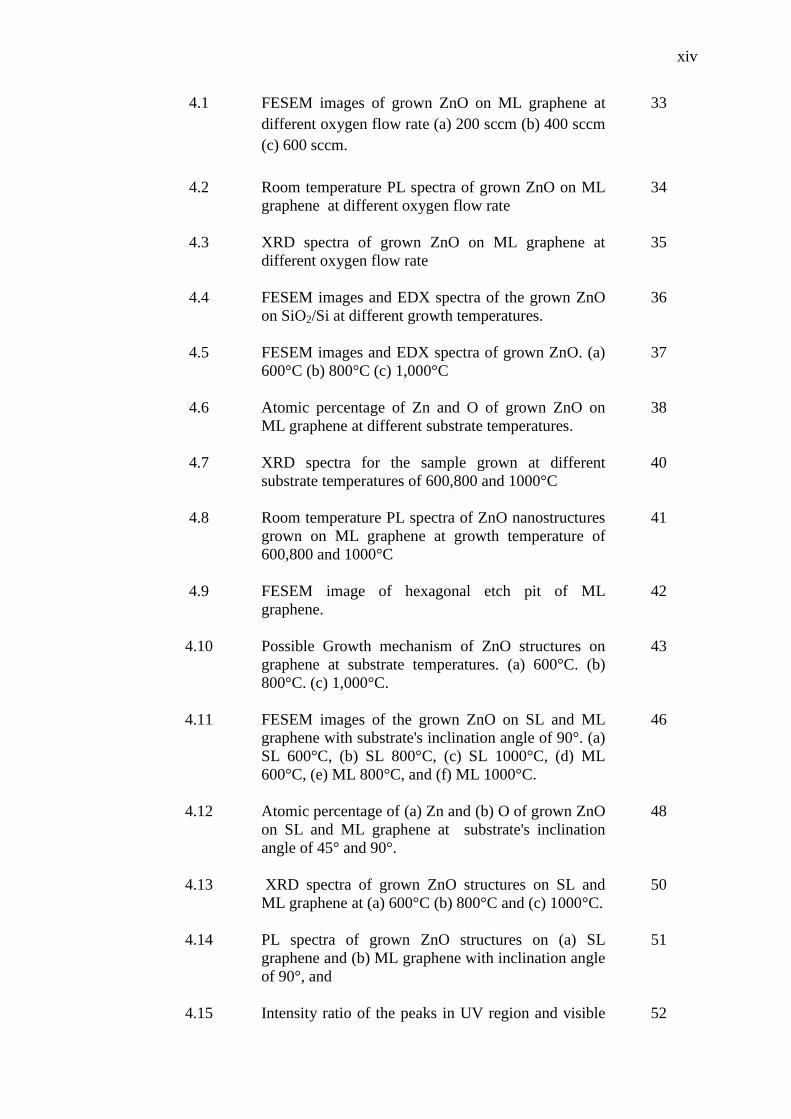
4.1
FESEM images of grown ZnO on ML graphene at
different oxygen flow rate (a) 200 sccm (b) 400 sccm
(c) 600 sccm.
33
4.2
Room temperature PL spectra of grown ZnO on ML
graphene at different oxygen flow rate
34
4.3
XRD spectra of grown ZnO on ML graphene at
different oxygen flow rate
35
4.4
FESEM images and EDX spectra of the grown ZnO
on SiO2/Si at different growth temperatures.
36
4.5
FESEM images and EDX spectra of grown ZnO. (a)
600°C (b) 800°C (c) 1,000°C
37
4.6
Atomic percentage of Zn and O of grown ZnO on
ML graphene at different substrate temperatures.
38
4.7
XRD spectra for the sample grown at different
substrate temperatures of 600,800 and 1000°C
40
4.8
Room temperature PL spectra of ZnO nanostructures
grown on ML graphene at growth temperature of
600,800 and 1000°C
41
4.9
FESEM image of hexagonal etch pit of ML
graphene.
42
4.10
Possible Growth mechanism of ZnO structures on
graphene at substrate temperatures. (a) 600°C. (b)
800°C. (c) 1,000°C.
43
4.11
FESEM images of the grown ZnO on SL and ML
graphene with substrate's inclination angle of 90°. (a)
SL 600°C, (b) SL 800°C, (c) SL 1000°C, (d) ML
600°C, (e) ML 800°C, and (f) ML 1000°C.
46
4.12
Atomic percentage of (a) Zn and (b) O of grown ZnO
on SL and ML graphene at substrate's inclination
angle of 45° and 90°.
48
4.13
XRD spectra of grown ZnO structures on SL and
ML graphene at (a) 600°C (b) 800°C and (c) 1000°C.
50
4.14
PL spectra of grown ZnO structures on (a) SL
graphene and (b) ML graphene with inclination angle
of 90°, and
51
4.15 Intensity ratio of the peaks in UV region and visible 52

xv
region.
4.16 Possible growth mechanism of ZnO structures. 53
xvi
LIST OF ABBREVIATIONS
1D - One dimensional
2D - Two dimensional
Ar - Argon
Au - Gold
CdO - Cadmium Oxide
CMOS - Complementary metal-oxide semiconductor
CNT - Carbon nanotube
CVD - Chemical Vapor Deposition
EDS - Energy dispersive X-ray spectrometer
FESEM - Field emission scanning electron microscopy
FET - Field effect transistor
GaAs - Gallium Arsenide
GaN - Gallium Nitride
Ge - Germanium
i-SoC - Intelligent system-on-chip
MgO - Magnesium oxide
ML - Multi layer
MOVPE - Metalorganic vapour phase epitaxy
O2 - Oxygen
PL - Photoluminscence
RT - Room temperature
Si - Silicon
xvii
Si3N4 - Silicon Nitride
SiC - Silicon Carbide
SiO2 - Silicon Dioxide
Si-ULSI - Silicon ultra-large-scale integrated circuits
SL - Single Layer
ST - Set temperature
TEM - Transmission electron microscopy
UV - Ultra violet
XRD - X-ray diffractometer
Zn - Zinc
ZnO - Zinc Oxide

xviii
LIST OF SYMBOLS
Ǻ - Angstroms, 1Ǻ = 1x10⁻¹⁰
m
°C
- Degree celcius
μm
- Micrometer
cm
- Centimeter
cm2/Vs
- carrier mobility
d
- Inter-plane distance in angstroms
eV
- Electron volt
IUV/IVIS
- Intensity ratio
kV
- Kilo Volt
n
- An integer 1,2,3
nm
- nanometer
meV
- Millielectron volt
Oi
- Oxygen interstitial
sccm
- Standard cubic centimeter per minute
Vo
- Oxygen vacancy
VZn
- Zinc vacancy
θ
- Diffraction angle in degree
λ
- Wavelength
W/mK - Thermal conductivity
m2/g - Surface area

xix
TPa - Young’s modulus
Zni
- Zn interstitial

xx
LIST OF APPENDIX
APPENDIX TITLE PAGE
A
Publications
71
CHAPTER 1
INTRODUCTION
1.1 Research background
We are currently living in the age of silicon nanotechnology. Silicon (Si)
based transistor drives a modern computing revolution year by year. The size of a
transistor has been reduced consistently which allows more transistors to be packed
onto a single chip, thereby increasing a computer power. This follows the Moore's
Law, according to which the number of transistors on a chip is doubling
approximately once every 2 years. Principally, the miniaturization of a transistor is
known to be very helpful in increasing an overall efficiency of the silicon ultra-large-
scale integrated circuits (Si-ULSIs). However, this unceasing miniaturization of
transistors is becoming increasingly difficult owing to the several limitations such as
short channel effect and gate leakage current etc.
In recent years, a concept of the advanced heterogeneous integration of the Si
platform has attracted much attention towards the recognition of a ‘More than
Moore’ technology [1]. To realize such technology, a growth of the high-quality
elements (i.e., germanium (Ge) [2]) compound semiconductors (i.e., gallium arsenide
(GaAs) [3], gallium nitride (GaN) [4], silicon carbide (SiC) [5]), metal oxides (i.e.,
zinc oxide (ZnO) [6]), and carbon-based materials (i.e., graphene [7], carbon
nanotube (CNT) [8]) on the Si platform is highly required. The co-integration of
these materials enables the present ultra-large-scale integrated circuits (ULSIs) to be
facilitated not only with ultra-high speed complementary metal-oxide semiconductor
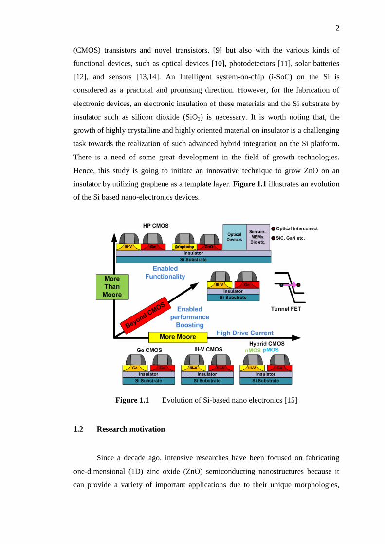
2
(CMOS) transistors and novel transistors, [9] but also with the various kinds of
functional devices, such as optical devices [10], photodetectors [11], solar batteries
[12], and sensors [13,14]. An Intelligent system-on-chip (i-SoC) on the Si is
considered as a practical and promising direction. However, for the fabrication of
electronic devices, an electronic insulation of these materials and the Si substrate by
insulator such as silicon dioxide (SiO2) is necessary. It is worth noting that, the
growth of highly crystalline and highly oriented material on insulator is a challenging
task towards the realization of such advanced hybrid integration on the Si platform.
There is a need of some great development in the field of growth technologies.
Hence, this study is going to initiate an innovative technique to grow ZnO on an
insulator by utilizing graphene as a template layer. Figure 1.1 illustrates an evolution
of the Si based nano-electronics devices.
Figure 1.1 Evolution of Si-based nano electronics [15]
1.2 Research motivation
Since a decade ago, intensive researches have been focused on fabricating
one-dimensional (1D) zinc oxide (ZnO) semiconducting nanostructures because it
can provide a variety of important applications due to their unique morphologies,

3
compositions, and chemical/physical properties [6,16]. Besides that, ZnO possesses
wide band gap and large exciton energy and it is considered to be a promising
candidate for the fabrication of several kinds of devices.
Meanwhile, at a room temperature (RT), the graphene retains a high carrier
mobility of up to 200,000 cm2/Vs [17], which can provide a long mean free path of
1.2 μm at a carrier concentration of 2 × 1011 cm-2
. At RT also, the quantum Hall
effect exist in graphene, owing to ballistic transport of electrons and holes [18]. This
ability makes graphene suitable for use in various ballistic device applications. It has
also been observed that the graphene possesses a very high thermal conductivity
(~5000 W/mK) [19-23]. Since graphene is an excellent conductor and transparent
material, the hybrid structure of ZnO/graphene shall lead to several device
applications not only on Si substrate but also on other insulating substrates such as
transparent glass and transparent flexible plastic
As mention previously, the growth of semiconductor materials on an insulator
such as SiO2 is challenging due to its amorphous structure. Therefore, an
introduction of graphene as a template layer is a promising candidate to overcome
this issue. The feasibility of growing, highly oriented single crystalline ZnO is one of
the main reasons of utilizing graphene as a buffer layer. The graphene consists of a
two-dimensional hexagonal network of carbon atoms which is formed by making
strong triangular σ-bonds of the sp2 hybridized orbitals. It is worth noting that the
atomic arrangement of graphene is similar to the (111) plane of zinc blence structure
and c-plane of a hexagonal crystalline structure which makes the growth of
semiconductor nanostructures and thin film on graphene feasible.
In this study, the formation of ZnO nanostructures on the graphene/SiO2/Si
substrates by the thermal evaporation process without any assist form catalyst is
carried out. The growth of ZnO nanostructures on the graphene is carried out by
using a simple thermal evaporation of Zn powder and oxygen (O2) gas under the
atmospheric pressure. The optimization of growth parameter such as substrate
temperature, oxygen flow rate, substrate inclination angles and graphene thickness
were investigated. Finally, the morphological, compositional, crystallographic and
4
optical properties of the as-grown ZnO nanostructures are systematically
characterised. The possible growth mechanism for the different geometrical
morphologies of the nanostructure is also proposed.
1.3 Objectives
To synthesize high density ZnO nanostructures on the graphene/SiO2/Si
substrate by thermal evaporation technique
i) To investigate the effect of oxygen flow rates, substrate temperatures
substrate inclination angles and graphene thicknesses on the surface
morphology, compositional crystallographic and optical properties of
ZnO nanostructures.
ii) To propose the reasonable growth mechanism based on the obtained
results.
1.4 Research activities
The implementation of this study has been summarized into a flowchart as
shown in Figure 1.2. This study is focused on the growth of one dimensional (1D)
ZnO nanostructures on the graphene by the thermal evaporation process without any
assistance of a catalyst. The growth was carried out by the thermal evaporation
technique in a dual zone furnace. Firstly, the growth of ZnO nanostructures was
investigated by varying the growth parameters (i.e. substrate temperatures, oxygen
flow rates, and substrate inclination angles and graphene thickness). The
morphological and elemental analysis of the grown ZnO nanostructures were
performed by using the field emission scanning electron microscopy (FESEM)
equipped with the electron dispersive spectrometer EDS. The crystallographic
properties were investigated using x-ray diffractometer (XRD) and the optical
properties are characterized using photoluminescence (PL) spectrometer. The
possible growth mechanism was proposed based on the obtained morphology.

5
Figure 1.2 Research activities
1.5 Thesis organization
This thesis has been organized into 5 chapters. Chapter 1 gives an overview
of the research background and motivation of the study. The objectives and research
activities of the present work are also presented in this chapter.
In chapter 2, an overview of the basic material properties of ZnO is presented.
The structural, electronic and optical properties of ZnO are described in order to
provide an in-depth knowledge of the ZnO materials. This chapter also explains the
material properties of graphene and its structural properties. The hybrid integration
of the ZnO and graphene and its possible applications are also presented. Besides
that, a brief description of the methods that is widely used to grow the ZnO
nanostructures, as well as its potential applications in the optoelectronic devices were
described.

6
In chapter 3, the properties of graphene substrate that have been used in this
work are described. The growth of ZnO nanostructures on the substrates by a simple
thermal evaporation process without any catalyst and the characterization techniques
employed are also described in detail.
In chapter 4, the growth of ZnO nanostructure on the graphene by a thermally
evaporated Zn powder in the presence of O2 gas is presented. The optimization of the
growth parameter such as substrate temperature, oxygen flow rate, substrate
inclination angles and graphene thickness were investigated. A basic study of the
morphological, compositional, and crystallographic and photoluminescence
properties of the grown ZnO are performed and the possible growth mechanism is
also proposed in this chapter.
Finally, chapter 5 concludes the contributions of the present work and
discusses the future research directions.

58
REFERENCES
1. Pillarisetty, R. Academic and Industry Research Progress in Germanium
Nanodevices. Nature. 2011. 479: 324-328.
2. Hashim, A. M., Anisuzzaman, M., Muta, S., Sadoh, T. and Miyao, M.
Epitaxial- Template Structure Utilizing Ge-On-Insulator Stripe Arrays With
Nanospacing For Advanced Heterogeneous Integration On Si Platform. Jpn.
J. Appl. Phys., 2012. 51:06FF04:01-06FF04:05.
3. Kai, M., Urata, R., Miller, D. A. B. and Harria J.S. Low-Temperature
Growth Of Gaas On Si Used For Ultrafast Photoconductive Switches. IEEE
J. Quantum Elect. 2004. 40(6):800–804.
4. Dadgar, A., Poschenrieder, M., Bläsing, J., Contreras, O., Bertram, F.,
Riemann, T., Reiher, A., Kunze, M., Daumiller, I., Krtschil, A., Diez, A.,
Kaluza, A., Modlich, A., Kamp, M., Christen, J., Ponce, F. A., Kohn, E. and
Krost, A. MOVPE Growth of GaN On Si(111) Substrates. J. Cryst. Growth.
2003. 248:556–562.
5. Astuti, B., Tanikawa, M., Rahman, S. F. A., Yasui, K. and Hashim, A. M.
Graphene as a Buffer Layer for Silicon Carbide-On-Insulator Structures.
Materials. 2012. 5(12):2270–2279.
6. Rusli, N. I., Tanikawa, M., Mahmood, M. R., Yasui, K. and Hashim, A. M.
Growth of High density Zinc Oxide Nanorods on Porous Silicon by Thermal
Evaporation.Materials.2012.5(12):2817–2832.
7. Kalita, G., Hirano, R., Ayhan, M. E. and Tanemura, M. Fabrication of a
Schottky Junction Diode With Direct Growth Graphene on Silicon by a Solid
Phase Reaction. J. Phys. D. Appl. Phys, 2013. 46(45):455103.
8. Hu, W., Gong, D., Chen, Z., Yuan, L., Saito, K., Grimes, C. A. and
Kichambare, P. Growth of Well-Aligned Carbon Nanotube Arrays on
Silicon Substratesusing Porous Alumina Film as a Nanotemplate. Appl. Phys.
Lett., 2001. 79(19):3083–3085.

59
9. Rahman, S. F. A., Kasai, S. and Hashim, A. M. Room Temperature
Nonlinear Operation of a Graphene-Based Three-Branch Nanojunction
Device with Chemical Doping. Appl. Phys. Lett., 2012. 100(19):193116.
10. Mazloumi, M., Mandal, H. S. and Xiaowu, T. Fabrication of Optical Device
Arrays Using Patterned Growth of ZnO Nanostructures. IEEE. T.
Nanotechnol., 2012. 11(3):444–447.
11. Wang, J. and Lee, S. Ge-photodetectors for Si-based Optoelectronic
Integration. Sensors, 2011. 11(12):696–718.
12. Razykov, T. M., Ferekides, C. S., Morel, D., Stefanakos, E., Ullal, H.S. and
Upadhyaya, H.M. Solar Photovoltaic Electricity: Current Status and Future
Prospects. Sol. Energy, 2011. 85:1580–1608.
13. Young, D. J., Du, J., Zorman, C. A. and Ko, W. H. High-temperature Single-
crystal 3C-SiC Capacitive Pressure Sensor. IEEE Sens. J. 2004. 4(4):464–
470.
14. Ahn, M.W., Park, K.S., Heo, J.H., Park, J.G., Kim, D.W., Choi, K.J., Lee,
J.H. and Hong, S.H. Gas Sensing Properties of Defect-controlled ZnO-
nanowire Gas Sensor. Appl. Phys. Lett., 2008. 93:263103.
15. Takagi, S. and Takenaka, M. III-V/Ge CMOS Technologies on Si Platform.
Symposium on VLSI Technology Digest of Technical Papers. IEEE. 2010. Pp.
147.
16. Jayah NA, Yahaya H, Mahmood MR, Terasako T, Yasui K, Hashim AM
: High electron mobility, low carrier concentration of hydrothermally grown
ZnO thin film on a-plane sapphire at low temperature.
[abstract]. International Conference on Solid State Devices and
Materials 2014, 198-199.
17. Bolotin, K. I. Sikes, K. J. Jiang, Z. Klima, M. Funderberg, G. Hone, J. Kim,
P. Stormer, H. L. Ultra High Electron Mobolity in Suspended Graphene.
Solid State Communication. 2008. 146: 351-355.
18. Novoselov, K. S. Jiang, Z. Zhang, Y. Morozov, S. V. Stomer, H. L. Zeitler,
U. Maan, J. C. Boebinger, G. S. Kim, P. Geim, A. K. Room Temperature
Quantum Hall Effect in Graphene. Science. 2007. 315: 1379.
19. Balandin, A. A. Thermal Properties of Graphene and Nanostructured Carbon
Materials. Nature Materials. 2011. 10: 569-581 .

60
20. Balandin, A. A. and Nika, D. L. Phonons in Low-dimensions: Engineering
Phonons in Nanostructures and Graphene. Materials Today. 2012. 15: 266-
279.
21. Chen, S. Wu, Q. Mishra, C. Kang, J. Zhung, H. Cho, K. Cai, W. Balandin, A.
A. Ruoff, R. S. Thermal Conductivity of Isotopically Modified Graphene.
Nature Materials. 2012. 11: 203-207.
22. Ghosh, S. Nika, D. L. Pokatilov, E. P. Balandin, A. A. Heat Conduction in
Graphene: Experimetal Study and Theoritical Interpretation. New Journal
Physics. 2009. 11: 09501201-09501220.
23. Wang, H. Maiyalagan, T. Wang, X. Review on Recent Progress in Nitrogen-
Doped Graphene Sysnthesis, Chatacterization and Its Potential Applications.
ACS Catalysis. 2:7 81-794
24. Wang, Z. L., Zinc Oxide Nanostructures: Growth, Properties and
Applications. J. Phys.: Condens. Matter. 2004. 16: R829-R858
25. Maksimov, O. Recent Advances and Novel Approaches of P-Type Doping of
Zinc Oxide. Rev. Adv. Mater. Sci. 2010. 24: 26-34.
26. Janotti, A. and Van de Walle, C. G. Fundamentals of Zinc Oxide as a
Semiconductor. Rep. Prog. Phys. 2009. 72: 1-29.
27. Vayssieres, L. Growth of Arrayed Nanorods and Nanowires of ZnO from
Aqueous Solutions. Advanced Materials. 2003. 15: 464-466.
28. Zheng, M. J., Zhang, L. D., Li, G. H. and Shen, W. Z. Fabrication and Optical
Properties of Large-Scale Uniform Zinc Oxide Nanowire Arrays by One-Step
Electrochemical Deposition Technique. Chem. Phys. Lett. 2002. 363: 123-
128.
29. Liu, C., Zapien, J. A., Yao, Y., Meng, X., Lee, C. S., Fan, S., Lifshitz, Y. and
Lee, S. T. High Density, Ordered Ultraviolet Light-Emitting ZnO Nanowire
Arrays. Adv. Mater. 2003. 15: 838-841.
30. Asif, M. H., Nur, O., Willander, M., Strålfors, P., Brännmark, C., Elinder, F.
Englund, U. H., Lu, J. and Hultman, L. Growth and Structure of ZnO
Nanorods on a Sub-Micrometer Glass Pipette and Their Application as
Intracellular Potentiometric Selective Ion Sensors. Materials. 2010. 3: 4657-
4667.
61
31. Elias, J., Tena-Zaera, R., Wang, G. -Y. and Levy-Clement, C. Conversion of
ZnO Nanowires into Nanotubes with Tailored Dimensions. Chem. Mater.
2008. 20: 6633-6637.
32. Yu, Q., Fu, W., Yu, C., Yang, H., Wei, R., Li, M., Liu, S., Sui, Y., Liu, Z.,
Yuan, M. and Zou, G. Fabrication and Optical Properties of Large-Scale ZnO
Nanotube Bundles via a Simple Solution Route. J. Phys. Chem. C 2007. 111:
17521-17526.
33. Tong, Y., Liu, Y. Shao, C., Liu, Y., Xu, C., Zhang, J., Lu, Y., Shen, D. and
Fan, X. Growth and Optical Properties of Faceted Hexagonal ZnO
Nanotubes. J. Phys. Chem. B. 2006. 110: 14714-14718.
34. Xu, L., Liao, Q., Zhang, J., Ai, X. and Xu, D. Single-Crystalline ZnO
Nanotube Arrays on Conductive Glass Substrates by Selective Disolution of
Electrodeposited ZnO Nanorods. J. Phys. Chem. C. 2007. 111 4549-4552.
35. Pan, Z. W., Dai, Z. R. and Wang, Z. L. Nanobelts of Semiconducting Oxides.
Science. 2001. 2001: 1947-1949.
36. Wang, W., Zeng, B., Yang, J., Poudel, B., Huang, J., Naughton, M. J. and
Ren, Z. Aligned Ultralong ZnO Nanobelts and Their Enhanced Field
Emission. Adv. Mater. 2006. 18: 3275-3278
37. Qiu, Y. and Yang, S. ZnO Nanotetrapods: Controlled Vapor-Phase Synthesis
and Application for Humidity Sensing. Adv. Funct. Mater. 2007. 17: 1345-
1352.
38. Xu, F., Yu, K., Li, G., Li, Q. and Zhu, Z. Synthesis and Field Emission of
Four Kinds of ZnO Nanostructures: Nanosleeve-Fishes, Radial Nanowire
Arrays, Nanocombs and Nanoflowers. Nanotechnology. 2006. 17:. 2855-
2859.
39. Castaneda, L. Synthesis and Characterization of ZnO Micro- and Nano-
Cages. Acta Mater. 2009. 57: 1385-1391.
40. Sun, X. W. and Yang, Y. ZnO Nanostructures and Their Applications. 1st ed.
Temasek Boulevard, Singapore: Pan Stanford Publishing Pte. Ltd. 2012.
41. Jagadish, C. and Pearton, S. J. Zinc Oxide Bulk, Thin Films and
Nanostructures : Processing,Properties and Applications. 1st. ed. Elsivier
science, 2006.

62
42. Dulub, O., Diebold, U. and Kresse, G. Novel Stabilization Mechanism on
Polar Surfaces: ZnO(0001)-Zn. Phys. Rev. Lett. 2003. 90: 1-4.
43. Lauritsen, J. V., Porsgaard, S., Rasmussen, M. K., Jensen, M. C. R.,
Bechstein, R., Meinander, K., Clausen, B. S., Helveg, S., Wahl, R., Kresse,
G. and Besenbacher, F. Stabilization Principles for Polar Surfaces of ZnO. J.
Am. Chem. Soc. 2011. 5: 5987-5994.
44. Woll, C. The Chemistry and Physics of Zinc Oxide Surfaces. Prog. Surf. Sci.
2007. 82: 55-120.
45. Pearton, S. J., Norton, D.P., Ip, K., Heo, Y. W. and Steiner, T. Recent
Progress in Processing and Properties of ZnO. Superlattices Microstruct.
2003. 34: 3-32.
46. Singh, S., Thiyagarajan, P., Mohan Kant, K., Anita, D, Thirupathiah, S.,
Rama, N., Tiwari, B., Kottaisamy, M, Ramachandra Rao, M. S. Structure,
Microstructure and Physical Properties of ZnO Based Materials in Various
Forms: Bulk, Thin Film and Nano. J. Phys. D: Appl. Phys. 2007. 40: 6312-
6327.
47. Özgür, Ü., Alivov, Ya. I., Liu, C., Teke, A., Reshchikov, M. A., Doğan, S.,
Avrutin, V., Cho, S. -J. and Morkoç, H. A Comprehensive Review of ZnO
Materials and Devices. J. Appl. Phys. 2005. 98: 1-103.
48. Janotti, A. and Van de Walle, C. G. Fundamentals of Zinc Oxide as a
Semiconductor. Rep. Prog. Phys. 2009. 72: 1-29.
49. Ahmad, M. and Zhu, J. ZnO Based Advanced Functional Nanostructures:
Synthesis, Properties and Applications. J. Mater. Chem. 2011. 21: 599-614.
50. Chang, P.-C., Chien, C. -J., Stichtenoth, D., Ronning, C. and Lu, J. G. Finite
Size Effect in ZnO Nanowires. Appl. Phys. Lett. 2007. 90: 1-3.
51. Arnold, M. S., Avouris, P., Zheng, W. P. and Zhong, L. W. Field-Effect
Transistors Based on Single Semiconducting Oxide Nanobelts. J. Phys.
Chem. B. 2003. 107: 659-663.
52. Park, W. I., Kim, J. S., Yi, G. -C., Bae, M. H. and Lee, H. -J. Fabrication and
Electrical Characteristics of High-Performance ZnO Nanorod Field-Effect
Transistors. Appl. Phys. Lett. 2004. 85: 5052-5054.
63
53. Fan, Z. and Lu, J. G. Electrical Properties of ZnO Nanowire Field Effect
Transistors Characterized with Scanning Probes. Appl. Phys. Lett. 2005. 86:
1-3.
54. Chen, C-Y., Chen, M-W., Ke, J-J., Lin, C-A., Retamal, J. R. D. and He, J-H.
Surface Effects on Optical and Electrical Properties of ZnO Nanostructures.
Pure Appl. Chem. 2010. 82: 2055-2073.
55. Chang, P-C., Fan, Z., Chien, C-J., Stichtenoth, D., Ronning, C. and Lu, J. G.
High-Performance ZnO Nanowire Field Effect Transistors. Appl. Phys. Lett.
2006. 89: 1-3.
56. Ju, S., Lee, K., Yoon, M. -H., Facchetti, A., Marks, T. J. and Janes, D. B.
High Performance ZnO Nanowire Field Effect Transistors with Organic Gate
Nanodielectrics: Effects of Metal Contacts and Ozone Treatment.
Nanotechnology. 2007. 155201: 1-7.
57. Chang, Y. -K. and Hong, F. C. -N. The Fabrication of ZnO Nanowire Field-
Effect Transistors Combining Dielectrophoresis and Hot-Pressing.
Nanotechnology. 2009. 20: 1-6.
58. Lee, C. -T. Fabrication Methods and Luminescent Properties of ZnO Materials
for Light-Emitting Diodes. Materials. 2010. 3: 2218-2259.
59. Bakti Utama, M. I., Zhang, J., Chen, R., Xu, X., Li, D., Sun, H. and Xiong,
Q. Synthesis and Optical Properties of II–VI 1D Nanostructures. Nanoscale.
2012. 4: 1422-1435.
60. Korsunska, N. O., Borkovska, L. V., Bulakh, B. M., Khomenkova, L. Yu.,
Kushnirenko, V. I. and Markevich, I. V. The Influence of Defect Drift in
External Electric Field on Green Luminescence of ZnO Single Crystals. J.
Lumin. 2003. 102–103: 733-736.
61. Casro Neto, A. H., Guinea, F., Peres, N. M. R., Novoselov, K. S. and Geim,
A. K. The electronic properties of graphene. Rev. Mod. Phys. 2009. 81: 109
62. Novoselov, K. S. Geim, A. K. Morozov, S. V. Jiang, D. katsnelson, M. I.
Grigorieva, I. V. Dubonos, S. V. Firsov, A. A. Two-Dimensional Gas of
Massless Direct Fermions in Graphene. Nature. 2005. 438: 197-200.
63. Zhang, Y. Tan, J. W. Stormer, H. L. Kim, P. Experimental Observation of the
Quantum Hall Effect and Berry’s Phase in Graphene. Nature. 2005. 438: 201-
204.

64
64. Han, M. Y. Oezyilmaz, B. Zhang, Y. Kim, P. Energy Band Gap Engineering
of Graphene Nanoribbons. Physic Review Letter. 2007. 98: 20680501-
20680505.
65. Lee, C. Wei, X. Kysar, J. W. Hone, J. Measurement of The Elatic Properties
of Intrinsic Strength of Mono Layer graphene . Science. 2008. 321: 385-388.
66. Bunch, J. S. Zande, A. M. van der. Verbridge, S. S. Frank, I. W. Tarenbaum,
D. M. Parpia, J. M. Craighead, H. G. McEuen, P. L. Electrochemical
Resonators From Graphene Sheets. Science. 2008. 315: 490-493.
67. Reich, S. maultazsch, J. Thomsen, C. Tight Binding Description of Graphene.
Physics Review B. 2002. 66: 03541201-03541205.
68. Kim, S-W., Park, H-K., Yi, M-S., Park, N-M., Park, J-H., Kim, S-H., Maeng,
S-L., Choi, C-J. and Moon, S-E. Epitaxial Growth of ZnO Nanowall
Networks on GaN/sapphire Substrates. Appl. Phys. Lett. 2007. 90:033107.
69. Hosono, E., Fujihara, S., Honma, I. and Zhou, H. The Fabrication of an
Upright-Standing Zinc Oxide Nanosheet for use in Dye-sensitized Solar
Cells. Adv. Mater. 2005. 17:2091–2094.
70. Wang, X., Ding, Y., Li, Z., Song, J. and Wang, Z. L. Single-crystal
Mesoporous ZnO Thin Films Composed of Nanowalls. J. Phys. Chem. C.
2009. 113:1791–1794.
71. Lee, C. J., Lee, T. J., Lyu, S. C., Zhang, Y., Ruh, H. and Lee HJ: Field
Emission from Well-Aligned Zinc Oxide Nanowires Grown at Low
Temperature. Appl. Phys. Lett. 2002. 81:3648.
72. Park, W. I., Yi, G. C., Kim, M. Y. and Pennycook, S. J. ZnO Nanoneedles
Grown vVrtically on Si Substrate by Non-catalytic Vapor-phase Epitaxy.
Adv. Mater. 2002. 14:1841–1843.
73. Xiang, J. H., Zhu, P. X., Masuda, Y., Okuya, M., Kaneko, S. and Koumoto,
K. Flexible Solar-Cell From Zinc Oxide Nanocrystalline Sheets Self-
Assembled by an In-Situ Electrodeposition Process. J. Nanosci. Nanotechnol.
2006. 6:1797–1801.
74. Jin M-J, Lee S-D, Shin K-S, Jeong S-W, Yoon DH, Jeon D, Lee I-H, Lee
DK, Kim S- W: Low-temperature Solution-based Growth of ZnO Nanorods
and Thin Films on Si Substrates. J. Nanosci. Nanotechnol. 2009, 9:7432–
7436.
65
75. Lee, K.Y., Kumar, B., Park, H-K., Choi, W. M., Choi, J-Y. and Kim, S-W.
Growth of High Quality ZnO Nanowires on Graphene. J. Nanosci.
Nanotechnol. 2012. 12:1551–1554.
76. Ahmad, N.F., Rusli, N. I., Mahmood, M. R., Yasui, K., Hashim, A. M.
Seed/catalyst-free Growth of Zinc Oxide Nanostructures on Multilayer
Graphene by Thermal Evaporation. Nanoscale Res. Lett. 2014, 9:83
77. Aziz, N. S. A., Mahmood, M. R., Yasui, K., Hashim, A. M. Seed/Catalyst-
FreeVertically Growth Of High Density electrodeposited Zinc Oxide
Nanostructures On A Single-Layer Graphene . Nanoscale Res. Lett. 2014.
9:95
78. Aziz, N. S. A., Nishiyama, T., Rusli, N. I., Mahmood, M. R., Yasui, K.,
Hashim, A. M. Seedless Growth Of Zinc Oxide Flower-Shape Structures on
Multilayer Graphene by Electrochemical Deposition . Nanoscale Res. Lett.
2014. 9:337
79. Kim, Y-J., Lee, J-H. and Yi, G-C. Vertically Aligned ZnO Nanostructures
Grown on Graphene Layers. Appl. Phys. Lett. 2009. 95:213101.
80. Kim, Y-J., Hadiyamarman, Yoon, A., Kim, M., Yi, G. C. and Liu, C.
Hydrothermal Grown ZnO Nanostructures on Few-layer Graphene Sheets.
Nanotechnology. 2011. 22:24603-24610.
81. Choi, W.M., Shin, K. S., Lee, H. S., Choi, D., Kim, K. H., Shin, H. J., Yoon,
S. M., Choi, J. Y., and Kim, S. W. Selective Growth of ZnO Nanorods on
SiO2/Si Substrate using a Graphene Buffer Layer. Nano Res. 2011. 4:440-
447.
82. Xu, C., Lee, J-H., Lee, J-C., Kim, B-S., Hwang, S. W. and Whang, D.
Electrochemical Growth of Vertically Aligned ZnO Nanorod Arrays on
Oxidized Bi-layer Graphene Electrode. Cryst. Eng. Comm. 2011. 13:6036-
6039.
83. Yi, G. C., Wang, C. and Park, W. I. ZnON: Synthesis, Characterization and
Applications. Semicond. Sci. Technol. 2005. 20:s22–s34.
84. Yi, J., Lee, J. M. and Park, W. I. Vertically Aligned ZnO Nanorods and
Graphene Hybrid Architectures for High-sensitive Flexible Gas Sensors.
Sens. Actuators B. Chem. 2011. 155:264–269.
66
85. Liu, J-y. Y., X-x, ZG-h., Y-k, W., Zhang, K., Pan, N. and Wang, X-P. High
Performance Ultraviolet Photodetector Fabricated with ZnO Nanoparticles-
Graphene Hybrid Structures. Chin. J. Chem. Phys. 2013. 26:225–230.
86. Yang, K., Xu, C., Huang, L., Zou, L. and Wang, H. Hybrid Nanostructure
Heterojunction Solar Cells Fabricated using Vertically Aligned ZnO
nanotubes grown on Reduced Graphene Oxide. Nanotechnology. 2011.
22:405401.
87. Lee, J. M., Yi, J., Lee, W. W., Jeong, H. Y., Jung, T., Kim, Y. and Park, W.
I. ZnO Nanorods-Graphene Hybrid Structures for Enhanced Current
Spreading and Light Extraction in GaN-based Light Emitting Diodes. Appl
Phys Lett 2012. 100:061107.
88. Morkoç, H. and Ü. Özgür, Zinc Oxide: Fundamentals, Materials and Device
Technology. Weinheim: Wiley-VCH Verlag GmbH & Co. KGaA. 2009.
89. Huang, Y. and C. M. Lieber, Integrated Nanoscale Electronics and
Optoelectronics: Exploring Nanoscale Science and Technology through
Semiconductor Nanowires. Pure Appl. Chem. 2004. 76: 2051–2068.
90. Antohe, V. A., Gence, L., Sivastava, S. K. and Piraux, L. Template-Free
Electrodeposition of Highly Oriented and Aspect-Ratio Controlled ZnO
Hexagonal Columnar Arrays. Nanotechnology. 2012. 23: 1-7.
91. Hassan, N. K., Hashim, M. R., Mahdi, M. A. and Allam, N. K. A. Catalyst-
Free Growth of ZnO Nanowires on Si (100) Substrates: Effect of Substrate
Position on Morphological, Structural and Optical Properties. ECS J. Solid
State Sci. Technol. 2012. 1: P86-P89.
92. Yao, I. C., Tseng, T. Y. and Lin, P. ZnO Nanorods Grown on Polymer
Substrates as UV Photodetectors. Sens. Actuators, B. 2012. 178: 26– 31.
93. Ridhuan, N. S., Lockman, Z., Aziz, A. A. and Razak, K. A. Properties of ZnO
Nanorods Arrays Growth via Low Temperature Hydrothermal Reaction. Adv.
Mater. Res. 2012. 364: 422-426.
94. Thahab, S. M. Preparation and Structural Characterizations of ZnO Nano-
Columns Grown on Porous Silicon/Silicon (PS/ Si(111)) by Thermal
Evaporation. Optoelectron. Adv. Mater. 2011. 5: 1107-1110.
67
95. Kar, S., Pal, B. N., Chaudhuri, S. and Chakravorty, D. One-Dimensional ZnO
Nanostructure Arrays: Synthesis and Characterization. J. Phys. Chem. B.
2006. 110: 4605-4611.
96. Srivatsa, K. M. K., Chhikara, D. and Kumar, M. S. Synthesis of Aligned
ZnO Nanorod Array on Silicon and Sapphire Substrates by Thermal
Evaporation Technique. J. Mater. Sci. Technol. 2011. 27: 701-706.
97. Cheng, Q. and Ostrikov, K. K. Temperature-Dependent Growth Mechanisms
of Low-Dimensional ZnO Nanostructures. Cryst.Eng.Comm. 2011. 13: 3455-
3461.
98. Calestani, D., Zha, M. Z., Zanotti, L., Villani, M. and Zappettini, A. Low
Temperature Thermal Evaporation Growth of Aligned ZnO Nanorods on
ZnO Film: A Growth Mechanism Promoted by Zn Nanoclusters on Polar
Surfaces. Cryst.Eng.Comm. 2011. 13: 1707-1712.
99. Umar, A., Kim, S. H., Kim, J. H., Al-Hajry, A. and Hahn, Y. B. Temperature-
Dependant Non-Catalytic Growth of Ultraviolet-Emitting ZnO
Nanostructures on Silicon Substrate by Thermal Evaporation Process. J.
Alloys Compd. 2008. 463: 516–521.
100. Chang, C. C. and Chang, C. S. Growth of ZnO Nanowires without Catalyst
on Porous Silicon. Jpn. J. Appl. Phys. 2004. 43: 8360-8364.
101. Pung, S. -W., Tee, C. -C, Choy, K. -L. and Hou, X. Growth Mechanism of
Au-Catalyzed ZnO Nanowires: VLS or VS-VLS? Adv. Mater. Res. 2012.
364: 333-337.
102. Wu, J. -J. and Liu, S. -C. Low-Temperature Growth of Well-Aligned ZnO
Nanorods by Chemical Vapor Deposition. Adv. Mater. 2002. 14: 215-218.
103. Yang, J. H., Zheng, J. H., Zhai, H. J. and Yang, L. L. Low Temperature
Hydrothermal Growth and Optical Properties of ZnO Nanorods. Cryst. Res.
Technol. 2009. 44: 87-91.
104. Bechelany, M., Amin, A., Brioude, A., Cornu, D. and Miele, P. ZnO
Nanotubes by Template-Assisted Sol–Gel Route. J. Nanopart. Res. 2012. 14:
1-7.
105. Kashif, M., Usman Ali, S. M., Ali, M. E., Abdulgafour, H. I., Hashim, U.,
Willander, M. and Hassan, Z. Morphological, Optical, and Raman
68
Characteristics of ZnO Nanoflakes Prepared via a Sol–Gel Method. Phys.
Status Solidi A. 2012. 209: 143-147.
106. Abdul Rahman, I. B., Ayob, M. T. M., Mohamed, F., Othman, N. K., Mohd
Lawi, R. L. and Radiman, S. Synthesis and Characterization of ZnO, CuO
and CuO/ZnO Nanoparticles by a Novel Sol-Gel Route under Ultrasonic
Conditions. Adv. Mater. Res. 2012. 545: 64-70.
107. Hassan, N. K., Hashim, M. R., Al-Douri, Y. and Al-Heuseen, K. Current
Dependence Growth of ZnO Nanostructures by Electrochemical Deposition
Technique. Int. J. Electrochem. Sci. 2012. 7: 4625-4635.
108. Amin, G., Asif, M. H., Zainelabdin, A., Zaman, S., Nur, O. and Willander,
M. Influence of pH, Precursor Concentration, Growth Time, and Temperature
on the Morphology of ZnO Nanostructures Grown by the Hydrothermal
Method. J. Nanomater. 2011. 2011: 1-9.
109. Cheng, C., Liu, B., Yang, H., Zhou, W., Sun, L., Chen, R., Yu, S. F., Zhang,
J., Gong, H., Sun, H. and Fan, H. J. Hierarchical Assembly of ZnO
Nanostructures on SnO2 Backbone Nanowires: Low-Temperature
Hydrothermal Preparation and Optical Properties. J. Am. Chem. Soc. 2009. 3:
3069-3076.
110. Yao, B. D., Chan, Y. F. and Wang, N. Formation of ZnO Nanostructures by a
Simple Way of Thermal Evaporation. Appl. Phys. Lett. 2002. 81: 757-759.
111. Yan, J. -F., Lu, Y. -M., Liang Hong, -W., Liu, Y., -C., Li, B. -H., Fan, X. - W.
and Zhou, J. -M. Growth and Properties of ZnO Nanotubes Grown on
Si(11 1) Substrate by Plasma-Assisted Molecular Beam Epitaxy. J. Cryst.
Growth. 2005. 280: 206-211.
112. Hassan, N. K., Hashim, M. R., Mahdi, M. A. and Allam, N. K. A Catalyst-
Free Growth of ZnO Nanowires on Si (100) Substrates: Effect of Substrate
Position on Morphological, Structural and Optical Properties. ECS J.
Solid State Sci. Technol. 2012. 1: P86-P89.
113. Lu Z, Heng X, Chakraborty A, Luo C. Growth of ultra-long ZnO microtubes
using a modified vapor-solid setup. Micromachines. 2014;5:1069–81.
114. Ferrari, A. C., Meyer, J. C., Scardaci, V., Casiraghi, C., Lazzeri, M., Mauri,
F., Piscanec, S., Jiang, D., Novoselov, K.S., Roth, S., Geim, A. K. Raman
Spectrum of Graphene and Graphene Layers. Phys Rev Lett 2006. 97:187401.

69
115. Duhee Y, Hyerim M, Hyeonsik C, JinSik C, JungAe C, BaeHo P: Variations
in the Raman spectrum as a function of the number of graphene layers. J
Korean Phys Soc 2009, 55:1299–1303.
116. Liu, L., Ryu, S., Tomasik, M. R., Stolyarova, E., Jung, N., Hybertsen, M. S.,
Steigerwald, M. L., Brus, L. E. and Flynn G. W. Graphene Oxidation:
Thickness Dependent Etching And Strong Chemical Doping. Nano Lett.
2008. 8:1965–1970.
117. Chroder, D. K. Semiconductor Material and Device Characterization. 3rd.
ed. Hoboken, New Jersey: John Wiley & Sons, Inc. 2006.
118. JEOL USA (2009). Scanning Electron Microscope A to Z, in Basic
Knowledge for using the SEM. [Brochure]. Peabody, MA: JEOL USA,
Inc.
119. Lili Yang. Synthesis and Characterization of ZnO Nanostructures. Ph.D.
Thesis, Linköping University, Norrköping; 2010.
120. Ahmad M, Sun H, Zhu J. Enhanced photoluminescence and field-emission
behavior of vertically well aligned arrays of In-doped ZnO nanowires. ACS
Appl Mater Interfaces. 2011;3:1299–305.
121. Mahmood, K., Park, S.S. and Sung, H. J. Enhanced Photoluminescence,
Raman Spectra and Field-emission Behavior of Indium-doped ZnO
Nanostructures. J. Mater. Chem. C. 2013. 1:3138–3149.
122. Huang, M. H., Wu, Y., Feick, H., Tran, N., Weber, E. and Yang, P. Catalytic
Growth of Zinc Oxide Nanowires by Vapor Transport. Adv. Mater. 2001.
13:113–116.


![Application of Bio-Pesticides To Improve Paddy Yield ...Mr Amin Hasmi 2; Ms. Siti Nurul Ain Aida Mohammad ; Ms Ayu Nadzirah Alias2 and Ms Nur Hanis Haszrudin! 2 [2] University Technology](https://img.pdfslide.us/doc/110x75/5e4895725590280d030e0d55/application-of-bio-pesticides-to-improve-paddy-yield-mr-amin-hasmi-2-ms-siti.jpg)


![[Topik 4] Dinar & Dirham- Penggunaan Terkini (Mazli Alias)](https://img.pdfslide.us/doc/110x75/559035051a28abff2c8b46ca/topik-4-dinar-dirham-penggunaan-terkini-mazli-alias.jpg)


![[Topik 4] Dinar & Dirham- Penggunaan Terkini 2010 (Mazli Alias)](https://img.pdfslide.us/doc/110x75/55bdd61fbb61ebad0a8b4809/topik-4-dinar-dirham-penggunaan-terkini-2010-mazli-alias.jpg)