Embed Size (px)
Citation preview
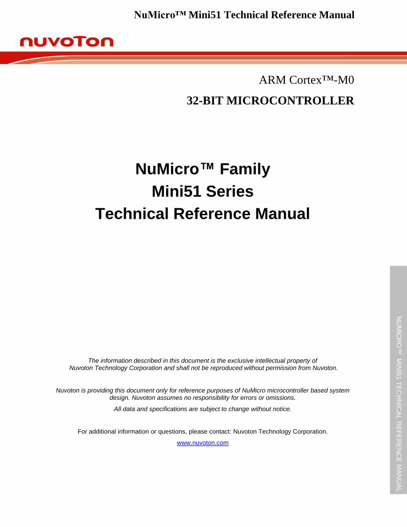
NuMicro™ Mini51 Technical Reference Manual
ARM Cortex™-M0
32-BIT MICROCONTROLLER
NU
MIC
RO
™ M
INI5
1 T
EC
HN
ICA
L R
EF
ER
EN
CE
MA
NU
AL
NuMicro™ Family
Mini51 Series
Technical Reference Manual
The information described in this document is the exclusive intellectual property of Nuvoton Technology Corporation and shall not be reproduced without permission from Nuvoton.
Nuvoton is providing this document only for reference purposes of NuMicro microcontroller based system design. Nuvoton assumes no responsibility for errors or omissions.
All data and specifications are subject to change without notice.
For additional information or questions, please contact: Nuvoton Technology Corporation.
www.nuvoton.com
NuMicro™ Mini51 Technical Reference Manual
Feb 9, 2012 Page 2 of 342 Revision V1.03
NU
MIC
RO
™ M
INI5
1 T
EC
HN
ICA
L R
EF
ER
EN
CE
MA
NU
AL
CONTENTS 1 GENERAL DESCRIPTION ................................................................................................... 10 2 FEATURES ........................................................................................................................... 11 3 PARTS INFORMATION LIST AND PIN CONFIGURATION ................................................ 14
3.1 NuMicro Mini51 Series Product Selection Guide .................................................... 14
3.2 PIN CONFIGURATION .............................................................................................. 15
3.2.1 LQFP 48-pin .................................................................................................................. 15 3.2.2 QFN 33-pin .................................................................................................................... 16
3.3 Pin Description ........................................................................................................... 17
4 BLOCK DIAGRAM ................................................................................................................ 21 4.1 NuMicro Mini51™ Block Diagram .............................................................................. 21
5 FUNCTIONAL DESCRIPTION .............................................................................................. 22 5.1 Memory Organization ................................................................................................. 22
5.1.1 Overview ........................................................................................................................ 22 5.1.2 System Memory Map ..................................................................................................... 23
5.2 Nested Vectored Interrupt Controller (NVIC) ............................................................. 24
5.2.1 Overview ........................................................................................................................ 24 5.2.2 Features ........................................................................................................................ 24 5.2.3 Exception Model and System Interrupt Map .................................................................. 24 5.2.4 Vector Table .................................................................................................................. 26 5.2.5 NVIC Operation ............................................................................................................. 27 5.2.6 NVIC Control Registers ................................................................................................. 28 5.2.7 Interrupt Source Control Registers ................................................................................ 41
5.3 System Manager ........................................................................................................ 47
5.3.1 Overview ........................................................................................................................ 47 5.3.2 System Reset ................................................................................................................ 47 5.3.3 System Power Distribution ............................................................................................. 47 5.3.4 Memory Mapping Table ................................................................................................. 49 5.3.5 System Manager Control Registers ............................................................................... 50
5.4 Clock Controller .......................................................................................................... 75
5.4.1 Overview ........................................................................................................................ 75 5.4.2 Clock Generator............................................................................................................. 75 5.4.3 System Clock and SysTick Clock .................................................................................. 76 5.4.4 AHB Clock Source Selection ......................................................................................... 77 5.4.5 Peripheral Clock Source Selection ................................................................................ 78 5.4.6 Power-down Mode Clock ............................................................................................... 80 5.4.7 Frequency Divider Output .............................................................................................. 81 5.4.8 Clock Control Register Map ........................................................................................... 82 5.4.9 Clock Control Register ................................................................................................... 83
5.5 Comparator Controller (CMPC) .................................................................................. 98
5.5.1 Overview ........................................................................................................................ 98 5.5.2 Features ........................................................................................................................ 98 5.5.3 Block Diagram ............................................................................................................... 99 5.5.4 Functional Description ................................................................................................. 100
NuMicro™ Mini51 Technical Reference Manual
Feb 9, 2012 Page 3 of 342 Revision V1.03
NU
MIC
RO
™ M
INI5
1 T
EC
HN
ICA
L R
EF
ER
EN
CE
MA
NU
AL
5.5.5 Comparator Reference Voltage (CRV) ........................................................................ 101 5.5.6 Register Map ............................................................................................................... 102 5.5.7 Register Description .................................................................................................... 103
5.6 Analog-to-Digital Converter (ADC) Controller .......................................................... 107
5.6.1 Overview ...................................................................................................................... 107 5.6.2 Features ...................................................................................................................... 107 5.6.3 Block Diagram ............................................................................................................. 108 5.6.4 ADC Operation Procedure ........................................................................................... 108 5.6.5 ADC Register Map ....................................................................................................... 111 5.6.6 ADC Register ............................................................................................................... 112
5.7 Flash Memory Controller (FMC) ............................................................................... 121
5.7.1 Overview ...................................................................................................................... 121 5.7.2 Features ...................................................................................................................... 121 5.7.3 Block Diagram ............................................................................................................. 121 5.7.4 Functional Description ................................................................................................. 123 5.7.5 Flash Control Register Map ......................................................................................... 133 5.7.6 Flash Control Register ................................................................................................. 134
5.8 General Purpose I/O ................................................................................................ 142
5.8.1 Overview ...................................................................................................................... 142 5.8.2 Features ...................................................................................................................... 142 5.8.3 Functional Description ................................................................................................. 142 5.8.4 Port 0-5 Control Register Map ..................................................................................... 145 5.8.5 Port 0-5 Control Register ............................................................................................. 149
5.9 I2C Serial Interface Controller (Master/Slave) .......................................................... 167
5.9.1 Overview ...................................................................................................................... 167 5.9.2 Features ...................................................................................................................... 167 5.9.3 I
2C Protocol.................................................................................................................. 168
5.9.4 I2C Protocol Registers ................................................................................................. 171
5.9.5 Register Mapping......................................................................................................... 174 5.9.6 Register Description .................................................................................................... 175 5.9.7 Operation Modes ......................................................................................................... 184 5.9.8 Master Transmitter Mode ............................................................................................. 184 5.9.9 Master Receiver Mode ................................................................................................. 184 5.9.10 Slave Receiver Mode ................................................................................................. 184 5.9.11 Slave Transmitter Mode ............................................................................................. 184 5.9.12 Data Transfer Flow in Five Operation Modes ............................................................ 184
5.10 Enhanced PWM Generator ...................................................................................... 191
5.10.1 Overview .................................................................................................................... 191 5.10.2 Features .................................................................................................................... 191 5.10.3 PWM Block Diagram .................................................................................................. 193 5.10.4 PWM Function ........................................................................................................... 195 5.10.5 PWM Operation Modes ............................................................................................. 203 5.10.6 Polarity Control .......................................................................................................... 204 5.10.7 PWM for Motor Control Interrupt Architecture ............................................................ 206 5.10.8 PWM Brake Function ................................................................................................. 206 5.10.9 PWM Controller Register Map ................................................................................... 207
NuMicro™ Mini51 Technical Reference Manual
Feb 9, 2012 Page 4 of 342 Revision V1.03
NU
MIC
RO
™ M
INI5
1 T
EC
HN
ICA
L R
EF
ER
EN
CE
MA
NU
AL
5.10.10 PWM Controller Register ......................................................................................... 208 5.11 Serial Peripheral Interface (SPI) Controller .............................................................. 228
5.11.1 Overview .................................................................................................................... 228 5.11.2 Features .................................................................................................................... 228 5.11.3 SPI Block Diagram ..................................................................................................... 228 5.11.4 Functional Description ............................................................................................... 229 5.11.5 SPI Serial Interface Control Register Map ................................................................. 239 5.11.6 Register Description .................................................................................................. 240
5.12 Timer Controller ........................................................................................................ 251
5.12.1 Overview .................................................................................................................... 251 5.12.2 Features .................................................................................................................... 251 5.12.3 Block Diagram ........................................................................................................... 252 5.12.4 Functional Description ............................................................................................... 253 5.12.5 Register Map ............................................................................................................. 257 5.12.6 Register Description .................................................................................................. 258
5.13 UART Interface Controller ........................................................................................ 267
5.13.1 Overview .................................................................................................................... 267 5.13.2 Features .................................................................................................................... 269 5.13.3 Block Diagram ........................................................................................................... 270 5.13.4 Functional Description ............................................................................................... 273 5.13.5 Registers Map............................................................................................................ 278 5.13.6 Register Description .................................................................................................. 279
5.14 Watchdog Timer ....................................................................................................... 302
5.14.1 Overview .................................................................................................................... 302 5.14.2 Features .................................................................................................................... 303 5.14.3 Block Diagram ........................................................................................................... 303 5.14.4 Watchdog Timer Control Registers Map .................................................................... 305 5.14.5 Register Description .................................................................................................. 306
6 ARM® CORTEX™-M0 CORE ............................................................................................. 309
6.1 Overview ................................................................................................................... 309
6.2 Features ................................................................................................................... 310
6.3 System Timer (SysTick) ........................................................................................... 311
6.3.1 System Timer Control Register Map ............................................................................ 312 6.3.2 System Timer Control Register .................................................................................... 313
6.4 System Control Registers ......................................................................................... 316
6.4.1 System Control Register Memory Map ........................................................................ 316 6.4.2 System Control Register .............................................................................................. 317
7 APPLICATION CIRCUIT ..................................................................................................... 324 8 ELECTRICAL CHARACTERISTICS ................................................................................... 325
8.1 Absolute Maximum Ratings ...................................................................................... 325
8.2 DC Electrical Characteristics .................................................................................... 326
8.3 AC Electrical Characteristics .................................................................................... 331
8.3.1 External Input Clock ..................................................................................................... 331 8.3.2 External 4 ~ 24 MHz XTAL Oscillator .......................................................................... 331
NuMicro™ Mini51 Technical Reference Manual
Feb 9, 2012 Page 5 of 342 Revision V1.03
NU
MIC
RO
™ M
INI5
1 T
EC
HN
ICA
L R
EF
ER
EN
CE
MA
NU
AL
8.3.3 Typical Crystal Application Circuit................................................................................ 331 8.3.4 External 32.768 KHz XTAL Oscillator .......................................................................... 332 8.3.5 Internal 22.1184 MHz RC Oscillator ............................................................................ 332 8.3.6 Internal 10 KHz RC Oscillator ...................................................................................... 333
8.4 Analog Characteristics ............................................................................................. 334
8.4.1 Brown-Out Reset (BOD) .............................................................................................. 334 8.4.2 Low Voltage Reset (LVR) ............................................................................................ 334 8.4.3 Analog Comparator ...................................................................................................... 334 8.4.4 Analog Comparator Reference Voltage (CRV) ............................................................ 335 8.4.5 10-bit ADC ................................................................................................................... 335 8.4.6 Flash Memory Characteristics ..................................................................................... 337
9 PACKAGE DIMENSION...................................................................................................... 338 9.1 48-pin LQFP ............................................................................................................. 338
9.2 33-pin QFN (4mm x 4mm) ........................................................................................ 339
9.3 33-pin QFN (5mm x 5mm) ........................................................................................ 340
10 REVISION HISTORY .......................................................................................................... 341
NuMicro™ Mini51 Technical Reference Manual
Feb 9, 2012 Page 6 of 342 Revision V1.03
NU
MIC
RO
™ M
INI5
1 T
EC
HN
ICA
L R
EF
ER
EN
CE
MA
NU
AL
List of Figures
Figure 3.1-1 NuMicro Mini51 Series Product Selection Guide .................................................... 14
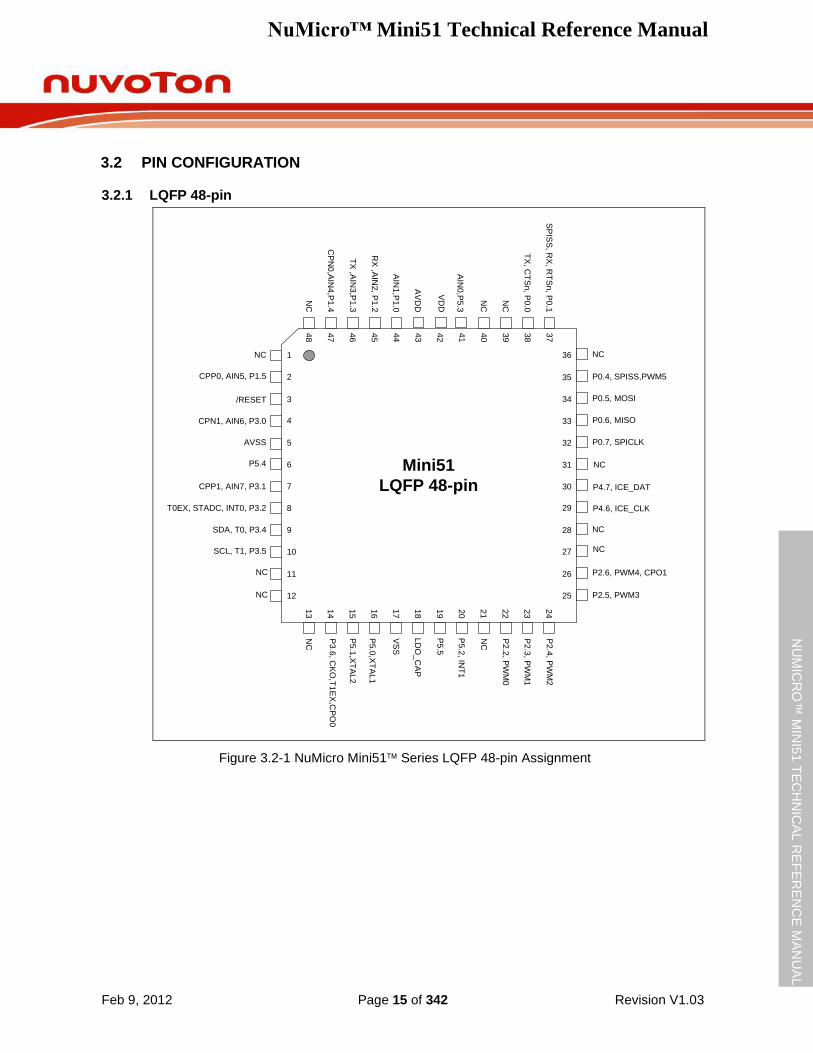
Figure 3.2-1 NuMicro Mini51 Series LQFP 48-pin Assignment .................................................. 15
Figure 3.2-2 NuMicro Mini51 Series QFN 33-pin Assignment .................................................... 16
Figure 4.1-1 NuMicro Mini51 Series Block Diagram ................................................................... 21
Figure 5.3-1 NuMicro Mini51 Series Power Distribution Diagram ............................................... 48
Figure 5.4-1 Clock Generator Block Diagram ................................................................................ 75
Figure 5.4-2 System Clock Block Diagram .................................................................................... 76
Figure 5.4-3 SysTick Clock Control Block Diagram ....................................................................... 76
Figure 5.4-4 AHB Clock Source for HCLK ..................................................................................... 77
Figure 5.4-5 Peripherals Clock Source Selection for PCLK ........................................................... 78
Figure 5.4-6 Clock Source of Frequency Divider ........................................................................... 81
Figure 5.4-7 Block Diagram of Frequency Divider ......................................................................... 81
Figure 5.5-1 Analog Comparator Block Diagram ........................................................................... 99
Figure 5.5-2 Comparator Controller Interrupt Sources ................................................................ 100
Figure 5.5-3 Comparator Reference Voltage Block Diagram ...................................................... 101
Figure 5.6-1 ADC Controller Block Diagram ................................................................................ 108
Figure 5.6-2 ADC Clock Control ................................................................................................... 109
Figure 5.6-3 A/D Conversion Result Monitor Logics Diagram ..................................................... 110
Figure 5.6-4 A/D Controller Interrupt ............................................................................................ 110
Figure 5.7-1 Flash Memory Control Block Diagram ..................................................................... 122
Figure 5.7-2 Flash Memory Organization ..................................................................................... 124
Figure 5.7-3 Flash Memory Structure .......................................................................................... 126
Figure 5.7-4 ISP Procedure.......................................................................................................... 130
Figure 5.7-5 ISP Operation Flow .................................................................................................. 131
Figure 5.8-1 Push-Pull Output ...................................................................................................... 143
Figure 5.8-2 Open-Drain Output .................................................................................................. 143
Figure 5.8-3 Quasi-bidirectional I/O Mode ................................................................................... 144
Figure 5.9-1 Bus Timing ............................................................................................................... 167
Figure 5.9-2 I2C Protocol .............................................................................................................. 168
Figure 5.9-3 Master Transmits Data to Slave .............................................................................. 168
Figure 5.9-4 Master Reads Data from Slave ................................................................................ 169
Figure 5.9-5 START and STOP Condition ................................................................................... 169
Figure 5.9-6 Bit Transfer on the I2C Bus ...................................................................................... 170
Figure 5.9-7 Acknowledge on the I2C Bus ................................................................................... 171
Figure 5.9-8 I2C Data Shifting Direction ....................................................................................... 172
NuMicro™ Mini51 Technical Reference Manual
Feb 9, 2012 Page 7 of 342 Revision V1.03
NU
MIC
RO
™ M
INI5
1 T
EC
HN
ICA
L R
EF
ER
EN
CE
MA
NU
AL
Figure 5.9-9 I2C Time-out Count Block Diagram .......................................................................... 173
Figure 5.9-10 Legend for the Following Five Figures .................................................................. 185
Figure 5.9-11 Master Transmitter Mode ....................................................................................... 186
Figure 5.9-12 Master Receiver Mode ........................................................................................... 187
Figure 5.9-13 Slave Transmitter Mode ......................................................................................... 188
Figure 5.9-14 Slave Receiver Mode ............................................................................................. 189
Figure 5.9-15 GC Mode ................................................................................................................ 190
Figure 5.10-1 Application Circuit Diagram ................................................................................... 192
Figure 5.10-2 PWM Block Diagram .............................................................................................. 193
Figure 5.10-3 PWM Generator 0 Architecture Diagram ............................................................... 193
Figure 5.10-4 PWM Generator 2 Architecture Diagram ............................................................... 194
Figure 5.10-5 PWM Generator 4 Architecture Diagram ............................................................... 194
Figure 5.10-6 Edge-aligned PWM ................................................................................................ 196
Figure 5.10-7 PWM Edge-aligned Waveform Output .................................................................. 196
Figure 5.10-8 Edge-aligned Flow Diagram .................................................................................. 197
Figure 5.10-9 Legend of Internal Comparator Output of PWM-Timer ......................................... 198
Figure 5.10-10 PWM Timer Operation Timing ............................................................................. 198
Figure 5.10-11 Center-aligned Mode ........................................................................................... 199
Figure 5.10-12 PWM Center-aligned Waveform Output .............................................................. 200
Figure 5.10-13 Center-aligned Flow Diagram (INT_TYPE = 0) ................................................... 201
Figure 5.10-14 PWM Double Buffering Illustration ....................................................................... 202
Figure 5.10-15 PWM Controller Output Duty Ratio ...................................................................... 202
Figure 5.10-16 Dead-zone Insertion ............................................................................................ 203
Figure 5.10-17 Initial State and Polarity Control with Rising Edge Dead-zone Insertion ............. 205
Figure 5.10-18 Motor Control PWM Architecture ......................................................................... 206
Figure 5.11-1 SPI Block Diagram ................................................................................................. 228
Figure 5.11-3 SPI Slave Mode Application Block Diagram .......................................................... 229
Figure 5.11-4 Two Transfer (Burst Mode) in One Transaction .................................................... 231
Figure 5.11-5 Word Suspend Mode ............................................................................................. 231
Figure 5.11-6 Byte Reorder .......................................................................................................... 232
Figure 5.11-7 Byte Suspend Mode .............................................................................................. 232
Figure 5.11-8 Variable Serial Clock Frequency ........................................................................... 233
Figure 5.11-9 SPI Timing in Master Mode ................................................................................... 234
Figure 5.11-10 SPI Timing in Master Mode (Alternate Phase of SPICLK) .................................. 235
Figure 5.11-11 SPI Timing in Slave Mode ................................................................................... 235
Figure 5.11-12 SPI Timing in Slave Mode (Alternate Phase of SPICLK) .................................... 236
NuMicro™ Mini51 Technical Reference Manual
Feb 9, 2012 Page 8 of 342 Revision V1.03
NU
MIC
RO
™ M
INI5
1 T
EC
HN
ICA
L R
EF
ER
EN
CE
MA
NU
AL
Figure 5.12-1 Timer Controller Block Diagram............................................................................. 252
Figure 5.12-2 Clock Source of Timer Controller........................................................................... 252
Figure 5.12-3 Continuous Counting Mode ................................................................................... 254
Figure 5.13-1 UART Clock Control Diagram ................................................................................ 270
Figure 5.13-2 UART Block Diagram ............................................................................................. 271
Figure 5.13-3 Auto Flow Control Block Diagram .......................................................................... 273
Figure 5.13-4 IrDA Block Diagram ............................................................................................... 274
Figure 5.13-5 IrDA TX/RX Timing Diagram .................................................................................. 275
Figure 5.13-6 Structure of RS-485 Frame.................................................................................... 277
Figure 5.14-1 Timing of Interrupt and Reset Signal ..................................................................... 303
Figure 5.14-2 Watchdog Timer Clock Control .............................................................................. 303
Figure 5.14-3 Watchdog Timer Block Diagram ............................................................................ 304
Figure 6.1-1 Functional Block Diagram ........................................................................................ 309
Figure 8.3-1 Typical Crystal Application Circuit ........................................................................... 332
NuMicro™ Mini51 Technical Reference Manual
Feb 9, 2012 Page 9 of 342 Revision V1.03
NU
MIC
RO
™ M
INI5
1 T
EC
HN
ICA
L R
EF
ER
EN
CE
MA
NU
AL
List of Tables
Table 3.3-1 NuMicro Mini51 Series Pin Description .................................................................... 20
Table 5.1-1 Address Space Assignments for On-Chip Modules.................................................... 23
Table 5.2-1 Exception Model ......................................................................................................... 25
Table 5.2-2 System Interrupt Map .................................................................................................. 26
Table 5.2-3 Vector Table Format ................................................................................................... 26
Table 5.3-1 Memory Mapping Table .............................................................................................. 49
Table 5.4-1 Peripherals Engine Clock Source Selection Table ..................................................... 79
Table 5.4-2 Power-down Mode Control Table ............................................................................... 85
Table 5.7-1 Memory Address Map ............................................................................................... 123
Table 5.7-2 Boot Selection Table ................................................................................................. 125
Table 5.7-3 Data Flash Table ....................................................................................................... 125
Table 5.7-4 Data Flash Configuration Example ........................................................................... 129
Table 5.7-5 ISP Command Table ................................................................................................. 132
Table 5.11-1 Byte Order and Byte Clock Idle Internal Conditions ............................................... 233
Table 5.12-1 Input Capture Mode Operation ............................................................................... 255
Table 5.13-1 UART Baud Rate Setting Table .............................................................................. 267
Table 5.13-2 UART Baud Rate Setting Table .............................................................................. 267
Table 5.13-3 UART Interrupt Sources and Flags Table In Software Mode ................................. 294
Table 5.13-4 UART Baud Rate Setting Table .............................................................................. 297
Table 5.14-1 Watchdog Time-out Interval Selection .................................................................... 302
NuMicro™ Mini51 Technical Reference Manual
Feb 9, 2012 Page 10 of 342 Revision V1.03
NU
MIC
RO
™ M
INI5
1 T
EC
HN
ICA
L R
EF
ER
EN
CE
MA
NU
AL
1 GENERAL DESCRIPTION
The NuMicro Mini51™ series 32-bit microcontroller is embedded with an ARM® Cortex™-M0 core
for industrial controls and applications which require high performance, high integration, and low cost. The Cortex™-M0 is the newest ARM embedded processor with 32-bit performance at a cost equivalent to the traditional 8-bit microcontroller.
The NuMicro Mini51™ series can run up to 24 MHz, and thus can afford to support a variety of industrial controls and applications requiring high CPU performance. The NuMicro Mini51™ series provides 4K/8K/16K-byte embedded program flash, size configurable data flash (shared with program flash), 2K-byte flash for the ISP, and 2K-byte embedded SRAM.
A number of system-level peripheral functions, such as I/O Port, Timer, UART, SPI, I2C, PWM,
ADC, Watchdog Timer, and low voltage detector, have been incorporated in the NuMicro Mini51™ series to reduce component count, board space, and system cost. These useful functions make the NuMicro Mini51™ series powerful for a wide range of applications.
Additionally, the NuMicro Mini51™ series is equipped with ISP (In-System Programming) and ICP (In-Circuit Programming) functions, allowing user to update program memory without removing a chip from an actual end product.
NuMicro™ Mini51 Technical Reference Manual
Feb 9, 2012 Page 11 of 342 Revision V1.03
NU
MIC
RO
™ M
INI5
1 T
EC
HN
ICA
L R
EF
ER
EN
CE
MA
NU
AL
2 FEATURES
Core
ARM® Cortex™-M0 core running up to 24 MHz
One 24-bit system timer
Supports low power Idle mode
A single-cycle 32-bit hardware multiplier
NVIC for 32 interrupt inputs, each with 4-level priority
Supports Serial Wire Debug (SWD) with 2 watchpoints/4 breakpoints
Built-in LDO for Wide Operating Voltage Range: 2.5V to 5.5V
Memory
4KB/8KB/16KB flash memory for program memory (APROM)
Configurable flash memory for data memory (Data Flash)
2KB flash memory for loader (LDROM)
2KB SRAM for internal scratch-pad RAM (SRAM)
In-System Programming (ISP) and In-Circuit Programming (ICP)
Clock Control
Programmable system clock source
Switch clock sources on-the-fly
4 ~ 24 MHz crystal oscillator (HXT)
32.768K crystal oscillator (LXT) for idle wake-up and system operation clock
22.1184 MHz internal oscillator (HIRC) (1% accuracy at 250C, 5V)
Dynamically calibrating the HIRC OSC to 22.0 MHz ±1% from -400C to 85
0C
by external 32.768K crystal oscillator (LXT)
10 KHz internal low-power oscillator (LIRC) for watchdog and idle wake-up
I/O Port
Up to 30 GPIO (General Purpose I/O) pins for LQFP-48 package
Software-configured I/O type
Quasi-bidirectional input/output
Push-pull output
Open-drain output
Input-only (high impendence)
Optional Schmitt trigger input
Timer
Two 24-bit Timers with 8-bit prescaler
Supports Event Counter mode
Supports Toggle Output mode
NuMicro™ Mini51 Technical Reference Manual
Feb 9, 2012 Page 12 of 342 Revision V1.03
NU
MIC
RO
™ M
INI5
1 T
EC
HN
ICA
L R
EF
ER
EN
CE
MA
NU
AL
Supports external trigger in Pulse Width Measurement mode
Supports external trigger in Pulse Width Capture mode
Watchdog Timer
Programmable clock source and time-out period
Supports wake-up function in Power-down mode and Idle mode
Interrupt or reset selectable when time-out happens
PWM
Up to three built-in 16-bit PWM generators with six PWM outputs or three complementary paired PWM outputs
Supports edge alignment or center alignment
Supports fault detection
Individual clock source, clock divider, 8-bit prescalar and dead-zone generator for each PWM generator
PWM interrupt synchronized to PWM period
UART (Universal Asynchronous Receiver/Transmitters)
One UART device
Buffered receiver and transmitter with 16-byte FIFO
Optional flow control function (CTSn and RTSn)
Supports IrDA (SIR) function
Programmable baud-rate generator up to 1/16 system clock
Supports RS-485 function
SPI (Serial Peripheral Interface)
One SPI device
Masters up to 12 MHz, and Slaves up to 4 MHz
Supports SPI Master/Slave mode
Full duplex synchronous serial data transfer
Variable length of transfer data from 1 to 32 bits
MSB or LSB first data transfer
Rx and Tx on both rising or falling edge of serial clock independently
Byte Suspend mode in 32-bit transmission
I2C
Supports Master/Slave mode
Bi-directional data transfer between masters and slaves
Multi-master bus (no central master)
Arbitration between simultaneously transmitting masters without corruption of serial data on the bus
Serial clock synchronization allowing devices with different bit rates to
NuMicro™ Mini51 Technical Reference Manual
Feb 9, 2012 Page 13 of 342 Revision V1.03
NU
MIC
RO
™ M
INI5
1 T
EC
HN
ICA
L R
EF
ER
EN
CE
MA
NU
AL
communicate via one serial bus
Serial clock synchronization used as a handshake mechanism to suspend and resume serial transfer
Programmable clocks allowing for versatile rate control
Supports multiple address recognition (4 slave addresses with mask option)
ADC (Analog-to-Digital Converter)
10-bit SAR ADC with 150K SPS
Up to 8-ch single-end input and one internal input from band-gap
Conversion started by software or external pin
Analog Comparator
Two analog comparators with programmable 16-level internal voltage reference
Built-in CRV (comparator reference voltage)
BOD (Brown-Out Detection) Reset
Three programmable threshold levels: 3.8V/2.7V/2.0V (default as 2.0V)
Optional BOD interrupt or reset
96-bit unique ID
Operating Temperature: -40℃~85℃
Packages:
Green package (RoHS)
LQFP 48-pin (7x7), QFN 33-pin (5x5), QFN 33-pin (4x4)
NuMicro™ Mini51 Technical Reference Manual
Feb 9, 2012 Page 14 of 342 Revision V1.03
NU
MIC
RO
™ M
INI5
1 T
EC
HN
ICA
L R
EF
ER
EN
CE
MA
NU
AL
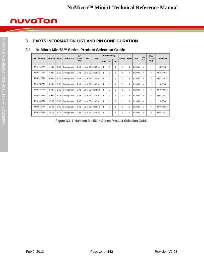
3 PARTS INFORMATION LIST AND PIN CONFIGURATION
3.1 NuMicro Mini51 Series Product Selection Guide
Part Number APROM RAM Data Flash ISP
Loader ROM
I/O Timer
Connectivity
Comp. PWM ADC ISP ICP
IRC 22.1184
MHz Package
UART SPI I2C
MINI51LAN 4 KB 2 KB Configurable 2 KB up to 30 2x32-bit 1 1 1 2 6 8x10-bit v v LQFP48
MINI51ZAN 4 KB 2 KB Configurable 2 KB up to 29 2x32-bit 1 1 1 2 6 8x10-bit v v QFN33(5x5)
MINI51TAN 4 KB 2 KB Configurable 2 KB up to 29 2x32-bit 1 1 1 2 6 8x10-bit v v QFN33(4x4)
MINI52LAN 8 KB 2 KB Configurable 2 KB up to 30 2x32-bit 1 1 1 2 6 8x10-bit v v LQFP48
MINI52ZAN 8 KB 2 KB Configurable 2 KB up to 29 2x32-bit 1 1 1 2 6 8x10-bit v v QFN33(5x5)
MINI52TAN 8 KB 2 KB Configurable 2 KB up to 29 2x32-bit 1 1 1 2 6 8x10-bit v v QFN33(4x4)
MINI54LAN 16 KB 2 KB Configurable 2 KB up to 30 2x32-bit 1 1 1 2 6 8x10-bit v v LQFP48
MINI54ZAN 16 KB 2 KB Configurable 2 KB up to 29 2x32-bit 1 1 1 2 6 8x10-bit v v QFN33(5x5)
MINI54TAN 16 KB 2 KB Configurable 2 KB up to 29 2x32-bit 1 1 1 2 6 8x10-bit v v QFN33(4x4)
Figure 3.1-1 NuMicro Mini51 Series Product Selection Guide
NuMicro™ Mini51 Technical Reference Manual
Feb 9, 2012 Page 15 of 342 Revision V1.03
NU
MIC
RO
™ M
INI5
1 T
EC
HN
ICA
L R
EF
ER
EN
CE
MA
NU
AL
3.2 PIN CONFIGURATION
3.2.1 LQFP 48-pin
2
44
1
4
3
6
5
8
7
10
9
11
48
42
41
40
39
38
37
32
33
30
31
28
29
26
27
25
13
14
15
16
18
19
20
21
22
12
17
23
24
34
35
36
46
47
43
45
Mini51
LQFP 48-pinN
C
CPP0, AIN5, P1.5
/RESET
AVSS
P5.4
CPP1, AIN7, P3.1
SDA, T0, P3.4
SCL, T1, P3.5
T0EX, STADC, INT0, P3.2
P5
.1,X
TA
L2
P5
.0,X
TA
L1
VS
S
P5
.2, IN
T1
LD
O_
CA
P
P2.2
, PW
M0
P2.3
, PW
M1
P2.4
, PW
M2
P5
.5
P3.6
, CK
O,T
1E
X,C
PO
0
P0.7, SPICLK
P4.6, ICE_CLK
P0.6, MISO
P0.5, MOSI
P0.4, SPISS,PWM5
P2.5, PWM3
P2.6, PWM4, CPO1
NC
P4.7, ICE_DAT
NC
TX
,AIN
3,P
1.3
RX
,AIN
2, P
1.2
CP
N0,A
IN4
,P1
.4
AIN
1,P
1.0
AIN
0,P
5.3
NC
AV
DD
NC
TX
, CT
Sn, P
0.0
SP
ISS
, RX
, RT
Sn, P
0.1
VD
D
NC
CPN1, AIN6, P3.0
NC
NC
NC
NC
NC
NC
Figure 3.2-1 NuMicro Mini51 Series LQFP 48-pin Assignment
NuMicro™ Mini51 Technical Reference Manual
Feb 9, 2012 Page 16 of 342 Revision V1.03
NU
MIC
RO
™ M
INI5
1 T
EC
HN
ICA
L R
EF
ER
EN
CE
MA
NU
AL
3.2.2 QFN 33-pin
CPP0,AIN5, P1.5
P5.4
CPN1,AIN6, P3.0
CPP1,AIN7, P3.1
SDA, T0, P3.4
SCL, T1, P3.5
P5
.1,X
TA
L2
P5
.0,X
TA
L1
VS
S
P5
.2,IN
T1
P2
.2, P
WM
0
P2
.3, P
WM
1
P2
.4, P
WM
2
P3
.6, C
KO
,T1
EX
,CP
O0
P0.7, SPICLK
P4.6, ICE_CLK
P0.6, MISO
P0.5, MOSI
P0.4, SPISS,PWM5
P2.5, PWM3
P2.6, PWM4,CPO1
P4.7, ICE_DAT
TX
, AIN
3, P
1.3
RX
, AIN
2, P
1.2
CP
N0
,AIN
4, P
1.4
AIN
1, P
1.0
TX
,CT
Sn
, P0
.0
VD
D
SP
ISS
,RX
,RT
Sn
, P0
.1
AIN
0,P
5.3
33 VSS
32
1 24
Mini51
QFN 33-pin
31 30 29 28 27 26 25
23
22
21
20
19
18
17
109 11 12 13 14 15 16
2
3
4
5
6
7
8
top transparent view
T0EX,STADC,INT0, P3.2
/RESET
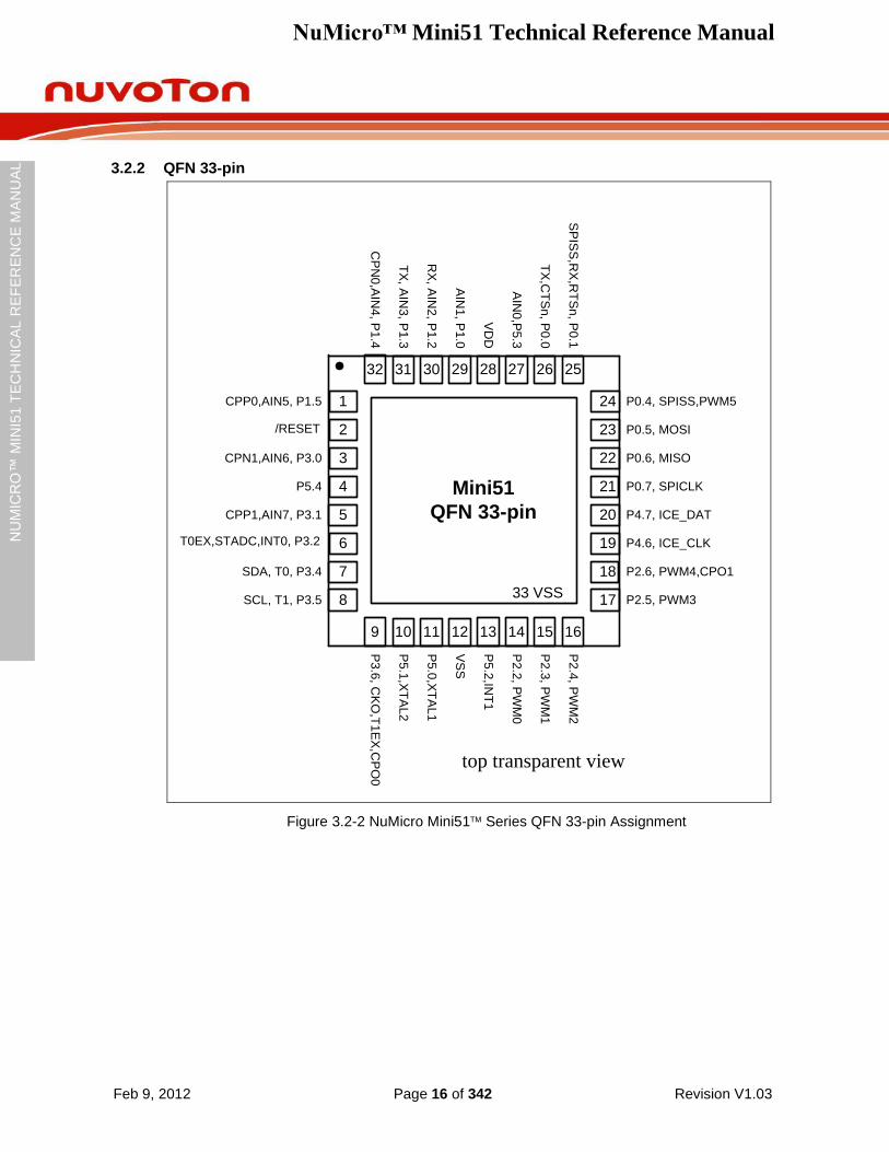
Figure 3.2-2 NuMicro Mini51 Series QFN 33-pin Assignment
NuMicro™ Mini51 Technical Reference Manual
Feb 9, 2012 Page 17 of 342 Revision V1.03
NU
MIC
RO
™ M
INI5
1 T
EC
HN
ICA
L R
EF
ER
EN
CE
MA
NU
AL
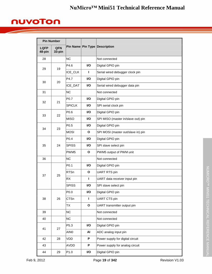
3.3 Pin Description
Pin Number
Pin Name Pin Type Description LQFP 48-pin
QFN 33-pin
1 NC Not connected
2 1
P1.5 I/O Digital GPIO pin
AIN5 AI ADC analog input pin
CPP0 AI Analog comparator Positive input pin
3 2 /RESET I(ST)
The Schmitt trigger input pin for hardware device reset. A “Low” on this pin for 768 clock counter of Internal RC
22.1184 MHz while the system clock is running will reset the device. /RESET pin has an internal pull-up resistor allowing power-on reset by simply connecting an external capacitor to GND.
4 3
P3.0 I/O Digital GPIO pin
AIN6 AI ADC analog input pin
CPN1 AI Analog comparator negative input pin
5 AVSS AP Ground pin for analog circuit
6 4 P5.4 I/O Digital GPIO pin
7 5
P3.1 I/O Digital GPIO pin
AIN7 AI ADC analog input pin
CPP1 AI Analog comparator positive input pin
8 6
P3.2 I/O Digital GPIO pin
INT0 I External interrupt 0 input pin
STADC I ADC external trigger input pin
T0EX I Timer 0 external capture/reset trigger input pin
9 7
P3.4 I/O Digital GPIO pin
T0 I/O Timer 0 external event counter input pin
SDA I/O I2C data I/O pin
10 8
P3.5 I/O Digital GPIO pin
T1 I/O Timer 1 external event counter input pin
SCL I/O I2C clock I/O pin
11 NC Not connected
12 NC Not connected
13 NC Not connected
NuMicro™ Mini51 Technical Reference Manual
Feb 9, 2012 Page 18 of 342 Revision V1.03
NU
MIC
RO
™ M
INI5
1 T
EC
HN
ICA
L R
EF
ER
EN
CE
MA
NU
AL
Pin Number
Pin Name Pin Type Description LQFP 48-pin
QFN 33-pin
14 9
P3.6 I/O Digital GPIO pin
CPO0 O Analog comparator output pin
CKO O Frequency divider output pin
T1EX I Timer 1 external capture/reset trigger input pin
15 10
P5.1 I/O Digital GPIO pin
XTAL2 O The output pin from the internal inverting amplifier. It emits the inverted signal of XTAL1.
16 11
P5.0 I/O Digital GPIO pin
XTAL1 I The input pin to the internal inverting amplifier. The system clock could be from external crystal or resonator.
17 12
VSS P Ground pin for digital circuit 33
18 LDO_CAP
P LDO output pin
19 P5.5 I/O
Digital GPIO pin
User program must enable pull-up resistor in the QFN-33 package.
20 13 P5.2 I/O Digital GPIO pin
INT1 I External interrupt 1 input pin
21 NC Not connected
22 14 P2.2 I/O Digital GPIO pin
PWM0 O PWM0 output of PWM unit
23 15 P2.3 I/O Digital GPIO pin
PWM1 O PWM1 output of PWM unit
24 16 P2.4 I/O Digital GPIO pin
PWM2 O PWM2 output of PWM unit
25 17 P2.5 I/O Digital GPIO pin
PWM3 O PWM3 output of PWM unit
26 18
P2.6 I/O Digital GPIO pin
PWM4 O PWM4 output of PWM unit
CPO1 O Analog comparator output pin
27 NC Not connected
NuMicro™ Mini51 Technical Reference Manual
Feb 9, 2012 Page 19 of 342 Revision V1.03
NU
MIC
RO
™ M
INI5
1 T
EC
HN
ICA
L R
EF
ER
EN
CE
MA
NU
AL
Pin Number
Pin Name Pin Type Description LQFP 48-pin
QFN 33-pin
28 NC Not connected
29 19 P4.6 I/O Digital GPIO pin
ICE_CLK I Serial wired debugger clock pin
30 20 P4.7 I/O Digital GPIO pin
ICE_DAT I/O Serial wired debugger data pin
31 NC Not connected
32 21 P0.7 I/O Digital GPIO pin
SPICLK I/O SPI serial clock pin
33 22 P0.6 I/O Digital GPIO pin
MISO I/O SPI MISO (master in/slave out) pin
34 23 P0.5 I/O Digital GPIO pin
MOSI O SPI MOSI (master out/slave in) pin
35 24
P0.4 I/O Digital GPIO pin
SPISS I/O SPI slave select pin
PWM5 O PWM5 output of PWM unit
36 NC Not connected
37 25
P0.1 I/O Digital GPIO pin
RTSn O UART RTS pin
RX I UART data receiver input pin
SPISS I/O SPI slave select pin
38 26
P0.0 I/O Digital GPIO pin
CTSn I UART CTS pin
TX O UART transmitter output pin
39 NC Not connected
40 NC Not connected
41 27 P5.3 I/O Digital GPIO pin
AIN0 AI ADC analog input pin
42 28 VDD P Power supply for digital circuit
43 AVDD P Power supply for analog circuit
44 29 P1.0 I/O Digital GPIO pin
NuMicro™ Mini51 Technical Reference Manual
Feb 9, 2012 Page 20 of 342 Revision V1.03
NU
MIC
RO
™ M
INI5
1 T
EC
HN
ICA
L R
EF
ER
EN
CE
MA
NU
AL
Pin Number
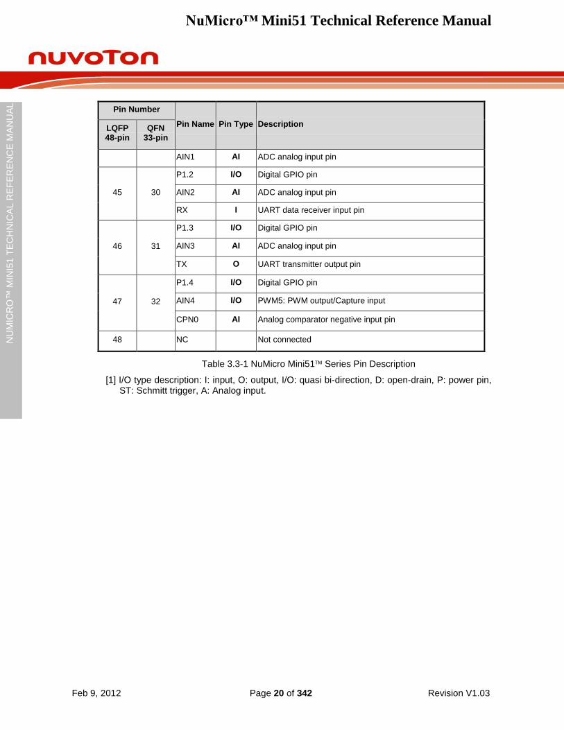
Pin Name Pin Type Description LQFP 48-pin
QFN 33-pin
AIN1 AI ADC analog input pin
45 30
P1.2 I/O Digital GPIO pin
AIN2 AI ADC analog input pin
RX I UART data receiver input pin
46 31
P1.3 I/O Digital GPIO pin
AIN3 AI ADC analog input pin
TX O UART transmitter output pin
47 32
P1.4 I/O Digital GPIO pin
AIN4 I/O PWM5: PWM output/Capture input
CPN0 AI Analog comparator negative input pin
48 NC Not connected
Table 3.3-1 NuMicro Mini51 Series Pin Description
[1] I/O type description: I: input, O: output, I/O: quasi bi-direction, D: open-drain, P: power pin, ST: Schmitt trigger, A: Analog input.
NuMicro™ Mini51 Technical Reference Manual
Feb 9, 2012 Page 21 of 342 Revision V1.03
NU
MIC
RO
™ M
INI5
1 T
EC
HN
ICA
L R
EF
ER
EN
CE
MA
NU
AL
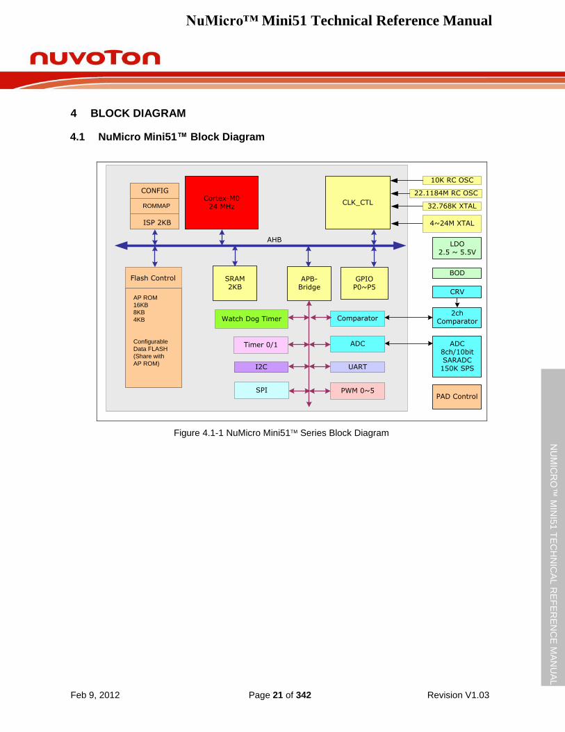
4 BLOCK DIAGRAM
4.1 NuMicro Mini51™ Block Diagram
Cortex-M024 MHz
CLK_CTL
AHB
APB-Bridge
GPIOP0~P5
ADC
Watch Dog Timer
I2C
SPI
UART
PWM 0~5
Timer 0/1
10K RC OSC
LDO2.5 ~ 5.5V
ADC8ch/10bitSARADC
150K SPS
PAD Control
BOD
AP ROM
16KB
8KB
4KB
Configurable
Data FLASH
(Share with
AP ROM)
Flash Control
ISP 4KB
Info
Option
ISP 2KB
CONFIG
ROMMAP
SRAM2KB
22.1184M RC OSC
4~24M XTAL
32.768K XTAL
Comparator2ch
Comparator
CRV
Figure 4.1-1 NuMicro Mini51 Series Block Diagram
NuMicro™ Mini51 Technical Reference Manual
Feb 9, 2012 Page 22 of 342 Revision V1.03
NU
MIC
RO
™ M
INI5
1 T
EC
HN
ICA
L R
EF
ER
EN
CE
MA
NU
AL
5 FUNCTIONAL DESCRIPTION
5.1 Memory Organization
5.1.1 Overview
The NuMicro Mini51 series provides a 4G-byte address space for programmers. The memory locations assigned to each on-chip modules are shown in Table 5.1-1. The detailed register and memory addressing and programming will be described in the following sections for individual on-
chip modules. The NuMicro Mini51 series only supports little-endian data format.
NuMicro™ Mini51 Technical Reference Manual
Feb 9, 2012 Page 23 of 342 Revision V1.03
NU
MIC
RO
™ M
INI5
1 T
EC
HN
ICA
L R
EF
ER
EN
CE
MA
NU
AL
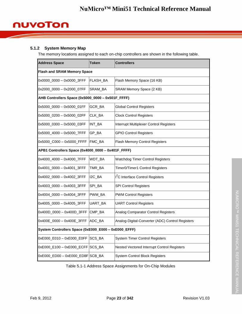
5.1.2 System Memory Map
The memory locations assigned to each on-chip controllers are shown in the following table.
Address Space Token Controllers
Flash and SRAM Memory Space
0x0000_0000 – 0x0000_3FFF FLASH_BA Flash Memory Space (16 KB)
0x2000_0000 – 0x2000_07FF SRAM_BA SRAM Memory Space (2 KB)
AHB Controllers Space (0x5000_0000 – 0x501F_FFFF)
0x5000_0000 – 0x5000_01FF GCR_BA Global Control Registers
0x5000_0200 – 0x5000_02FF CLK_BA Clock Control Registers
0x5000_0300 – 0x5000_03FF INT_BA Interrupt Multiplexer Control Registers
0x5000_4000 – 0x5000_7FFF GP_BA GPIO Control Registers
0x5000_C000 – 0x5000_FFFF FMC_BA Flash Memory Control Registers
APB1 Controllers Space (0x4000_0000 – 0x401F_FFFF)
0x4000_4000 – 0x4000_7FFF WDT_BA Watchdog Timer Control Registers
0x4001_0000 – 0x4001_3FFF TMR_BA Timer0/Timer1 Control Registers
0x4002_0000 – 0x4002_3FFF I2C_BA I2C Interface Control Registers
0x4003_0000 – 0x4003_3FFF SPI_BA SPI Control Registers
0x4004_0000 – 0x4004_3FFF PWM_BA PWM Control Registers
0x4005_0000 – 0x4005_3FFF UART_BA UART Control Registers
0x400D_0000 – 0x400D_3FFF CMP_BA Analog Comparator Control Registers
0x400E_0000 – 0x400E_3FFF ADC_BA Analog-Digital-Converter (ADC) Control Registers
System Controllers Space (0xE000_E000 – 0xE000_EFFF)
0xE000_E010 – 0xE000_E0FF SCS_BA System Timer Control Registers
0xE000_E100 – 0xE000_ECFF SCS_BA Nested Vectored Interrupt Control Registers
0xE000_ED00 – 0xE000_ED8F SCB_BA System Control Block Registers
Table 5.1-1 Address Space Assignments for On-Chip Modules
NuMicro™ Mini51 Technical Reference Manual
Feb 9, 2012 Page 24 of 342 Revision V1.03
NU
MIC
RO
™ M
INI5
1 T
EC
HN
ICA
L R
EF
ER
EN
CE
MA
NU
AL
5.2 Nested Vectored Interrupt Controller (NVIC)
5.2.1 Overview
The Cortex™-M0 CPU provides an interrupt controller as an integral part of the exception mode, named “Nested Vectored Interrupt Controller (NVIC)”. It is closely coupled to the processor kernel and provides the following features.
5.2.2 Features
Nested and Vectored interrupt support
Automatic processor state saving and restoration
Dynamic priority change
Reduced and deterministic interrupt latency
The NVIC prioritizes and handles all supported exceptions. All exceptions are handled in “Handler mode”. This NVIC architecture supports 32 (IRQ[31:0]) discrete interrupts with 4 levels of priority. All of the interrupts and most of the system exceptions can be configured to different priority levels. When an interrupt occurs, the NVIC will compare the priority of the new interrupt to the current running one‟s priority. If the priority of the new interrupt is higher than the current one, the new interrupt handler will override the current handler.
When an interrupt is accepted, the starting address of the Interrupt Service Routine (ISR) is fetched from a vector table in memory. There is no need to determine which interrupt is accepted and branch to the starting address of the correlated ISR by software. While the starting address is fetched, the NVIC will also automatically save the processor state including the registers “PC, PSR, LR, R0~R3, R12” to the stack. At the end of the ISR, the NVIC will restore the mentioned registers from stack and resume the normal execution. Thus it will take less and deterministic time to process the interrupt request.
The NVIC supports “Tail Chaining” which handles back-to-back interrupts efficiently without the overhead of states saving and restoration and therefore reduces delay time in switching to pending ISR at the end of current ISR. The NVIC also supports “Late Arrival” which improves the efficiency of concurrent ISRs. When a higher priority interrupt request occurs before the current ISR starts to execute (at the stage of state saving and starting address fetching), the NVIC will give priority to the higher one without delay penalty. Thus it advances the real-time capability.
For more detailed information, please refer to the “ARM® Cortex™-M0 Technical Reference
Manual” and “ARM® v6-M Architecture Reference Manual”.
5.2.3 Exception Model and System Interrupt Map
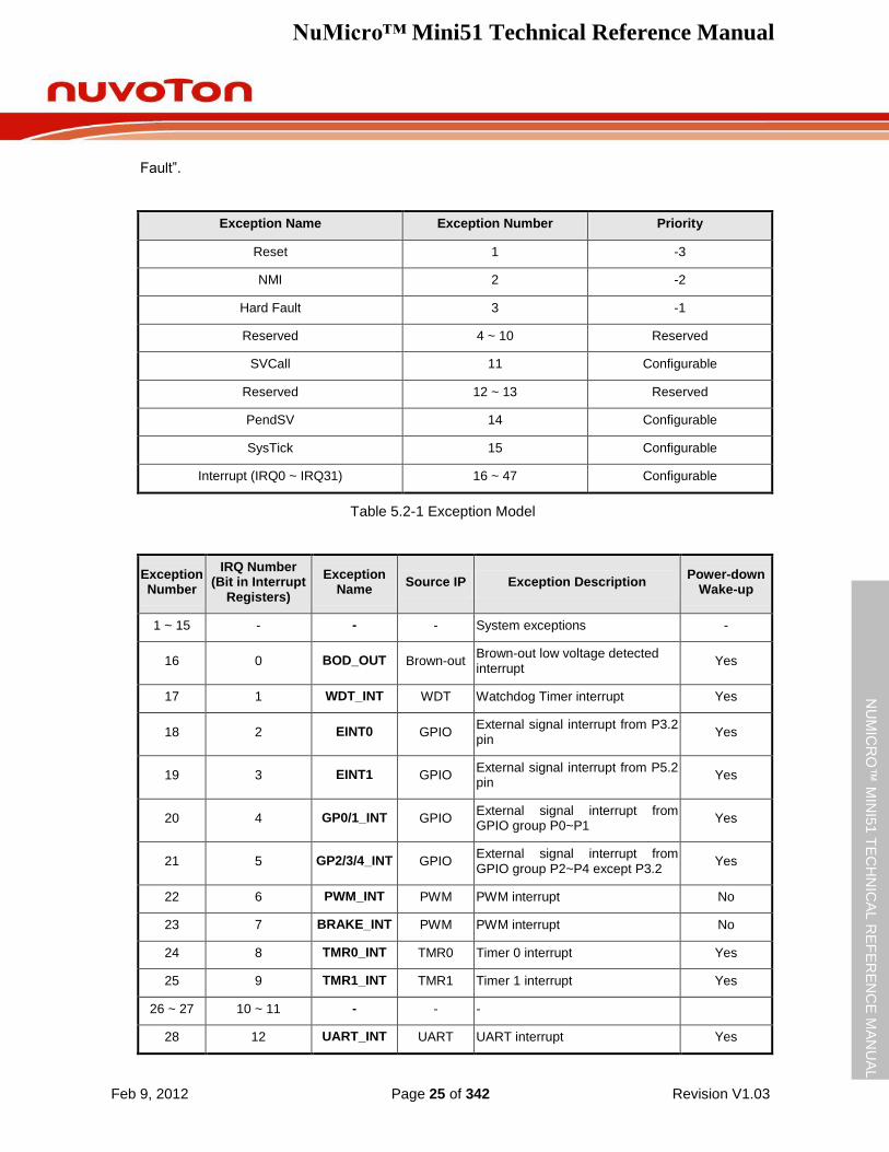
The exception model supported by the NuMicro Mini51 series is listed in the following table. Software can set four levels of priority on some of these exceptions as well as on all interrupts. The highest user-configurable priority is denoted as “0” and the lowest priority is denoted as “3”. The default priority of all the user-configurable interrupts is “0”. Note that the priority “0” is treated as the fourth priority on the system, after the three system exceptions “Reset”, “NMI” and “Hard
NuMicro™ Mini51 Technical Reference Manual
Feb 9, 2012 Page 25 of 342 Revision V1.03
NU
MIC
RO
™ M
INI5
1 T
EC
HN
ICA
L R
EF
ER
EN
CE
MA
NU
AL
Fault”.
Exception Name Exception Number Priority
Reset 1 -3
NMI 2 -2
Hard Fault 3 -1
Reserved 4 ~ 10 Reserved
SVCall 11 Configurable
Reserved 12 ~ 13 Reserved
PendSV 14 Configurable
SysTick 15 Configurable
Interrupt (IRQ0 ~ IRQ31) 16 ~ 47 Configurable
Table 5.2-1 Exception Model
Exception Number
IRQ Number (Bit in Interrupt
Registers)
Exception Name
Source IP Exception Description Power-down
Wake-up
1 ~ 15 - - - System exceptions -
16 0 BOD_OUT Brown-out Brown-out low voltage detected interrupt
Yes
17 1 WDT_INT WDT Watchdog Timer interrupt Yes
18 2 EINT0 GPIO External signal interrupt from P3.2 pin
Yes
19 3 EINT1 GPIO External signal interrupt from P5.2 pin
Yes
20 4 GP0/1_INT GPIO External signal interrupt from GPIO group P0~P1
Yes
21 5 GP2/3/4_INT GPIO External signal interrupt from GPIO group P2~P4 except P3.2
Yes
22 6 PWM_INT PWM PWM interrupt No
23 7 BRAKE_INT PWM PWM interrupt No
24 8 TMR0_INT TMR0 Timer 0 interrupt Yes
25 9 TMR1_INT TMR1 Timer 1 interrupt Yes
26 ~ 27 10 ~ 11 - - -
28 12 UART_INT UART UART interrupt Yes
NuMicro™ Mini51 Technical Reference Manual
Feb 9, 2012 Page 26 of 342 Revision V1.03
NU
MIC
RO
™ M
INI5
1 T
EC
HN
ICA
L R
EF
ER
EN
CE
MA
NU
AL
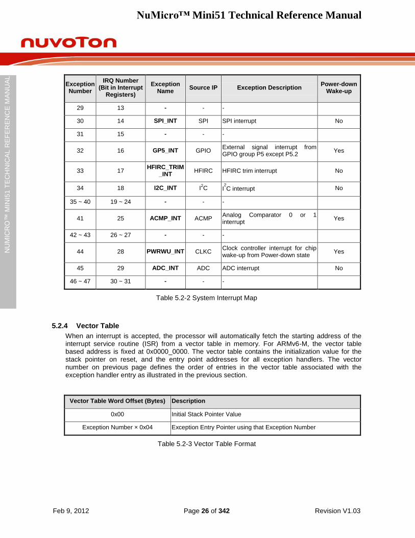
Exception Number
IRQ Number (Bit in Interrupt
Registers)
Exception Name
Source IP Exception Description Power-down
Wake-up
29 13 - - -
30 14 SPI_INT SPI SPI interrupt No
31 15 - - -
32 16 GP5_INT GPIO External signal interrupt from GPIO group P5 except P5.2
Yes
33 17 HFIRC_TRIM
_INT HFIRC HFIRC trim interrupt No
34 18 I2C_INT I2C I
2C interrupt No
35 ~ 40 19 ~ 24 - - -
41 25 ACMP_INT ACMP Analog Comparator 0 or 1 interrupt
Yes
42 ~ 43 26 ~ 27 - - -
44 28 PWRWU_INT CLKC Clock controller interrupt for chip wake-up from Power-down state
Yes
45 29 ADC_INT ADC ADC interrupt No
46 ~ 47 30 ~ 31 - - -
Table 5.2-2 System Interrupt Map
5.2.4 Vector Table
When an interrupt is accepted, the processor will automatically fetch the starting address of the interrupt service routine (ISR) from a vector table in memory. For ARMv6-M, the vector table based address is fixed at 0x0000_0000. The vector table contains the initialization value for the stack pointer on reset, and the entry point addresses for all exception handlers. The vector number on previous page defines the order of entries in the vector table associated with the exception handler entry as illustrated in the previous section.
Vector Table Word Offset (Bytes) Description
0x00 Initial Stack Pointer Value
Exception Number × 0x04 Exception Entry Pointer using that Exception Number
Table 5.2-3 Vector Table Format
NuMicro™ Mini51 Technical Reference Manual
Feb 9, 2012 Page 27 of 342 Revision V1.03
NU
MIC
RO
™ M
INI5
1 T
EC
HN
ICA
L R
EF
ER
EN
CE
MA
NU
AL
5.2.5 NVIC Operation
NVIC interrupts can be enabled or disabled by writing to their corresponding Interrupt Set-Enable or Interrupt Clear-Enable register bit-field. The registers use a write-1-to-enable and write-1-to-clear policy, and both registers reading back the current enabled state of the corresponding interrupts. When an interrupt is disabled, interrupt assertion will cause the interrupt to become Pending; however, the interrupt will not be activated. If an interrupt is Active when it is disabled, it remains in its Active state until cleared by reset or an exception return. Clearing the enable bit prevents new activations of the associated interrupt.
NVIC interrupts can be pended/un-pended using a complementary pair of registers to those used to enable/disable the interrupts, named the Set-Pending Register and Clear-Pending Register respectively. The registers use a write-1-to-enable and write-1-to-clear policy, both registers reading back the current pended state of the corresponding interrupts. The Clear-Pending Register has no effect on the execution status of an Active interrupt.
NVIC interrupts are prioritized by updating an 8-bit field within a 32-bit register (each register supporting four interrupts).
The general registers associated with the NVIC are all accessible from a block of memory in the System Control Space and will be described in the next section.
NuMicro™ Mini51 Technical Reference Manual
Feb 9, 2012 Page 28 of 342 Revision V1.03
NU
MIC
RO
™ M
INI5
1 T
EC
HN
ICA
L R
EF
ER
EN
CE
MA
NU
AL
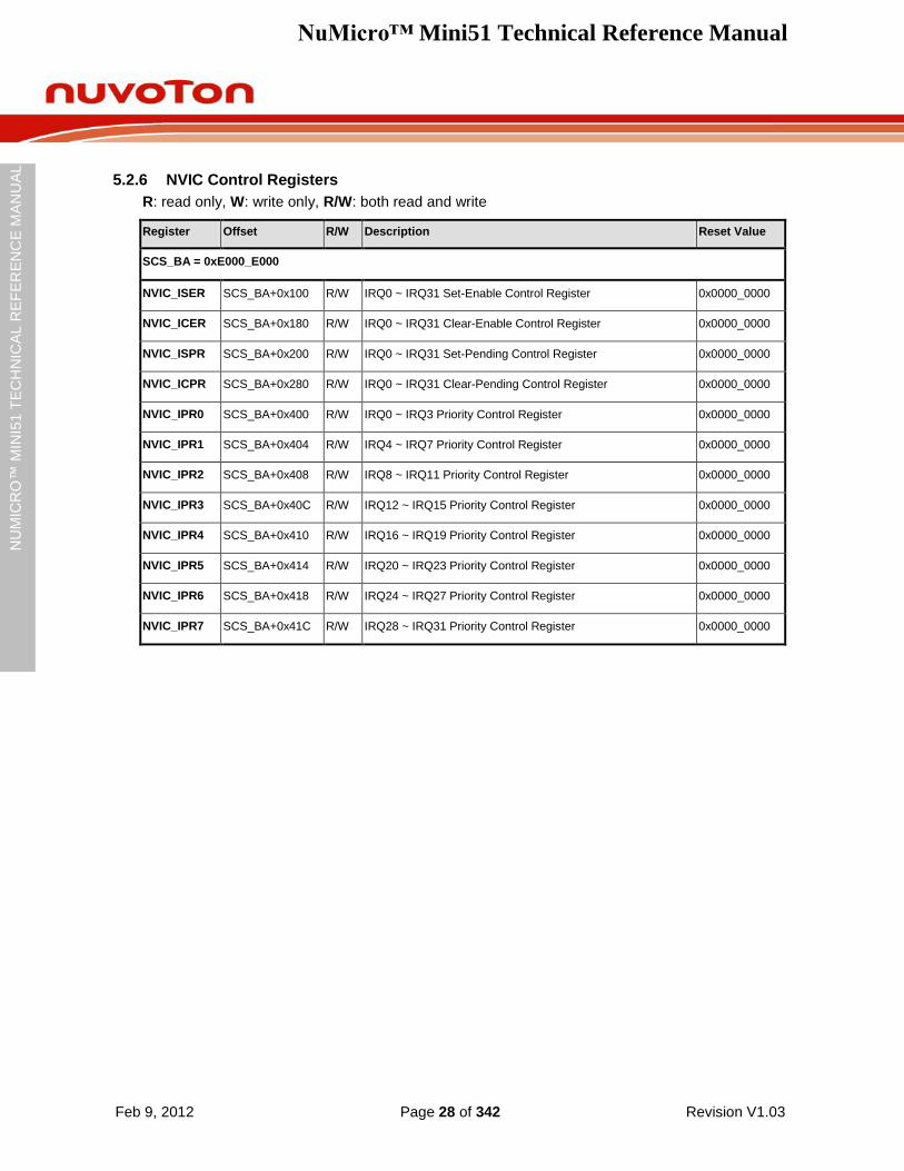
5.2.6 NVIC Control Registers
R: read only, W: write only, R/W: both read and write
Register Offset R/W Description Reset Value
SCS_BA = 0xE000_E000
NVIC_ISER SCS_BA+0x100 R/W IRQ0 ~ IRQ31 Set-Enable Control Register 0x0000_0000
NVIC_ICER SCS_BA+0x180 R/W IRQ0 ~ IRQ31 Clear-Enable Control Register 0x0000_0000
NVIC_ISPR SCS_BA+0x200 R/W IRQ0 ~ IRQ31 Set-Pending Control Register 0x0000_0000
NVIC_ICPR SCS_BA+0x280 R/W IRQ0 ~ IRQ31 Clear-Pending Control Register 0x0000_0000
NVIC_IPR0 SCS_BA+0x400 R/W IRQ0 ~ IRQ3 Priority Control Register 0x0000_0000
NVIC_IPR1 SCS_BA+0x404 R/W IRQ4 ~ IRQ7 Priority Control Register 0x0000_0000
NVIC_IPR2 SCS_BA+0x408 R/W IRQ8 ~ IRQ11 Priority Control Register 0x0000_0000
NVIC_IPR3 SCS_BA+0x40C R/W IRQ12 ~ IRQ15 Priority Control Register 0x0000_0000
NVIC_IPR4 SCS_BA+0x410 R/W IRQ16 ~ IRQ19 Priority Control Register 0x0000_0000
NVIC_IPR5 SCS_BA+0x414 R/W IRQ20 ~ IRQ23 Priority Control Register 0x0000_0000
NVIC_IPR6 SCS_BA+0x418 R/W IRQ24 ~ IRQ27 Priority Control Register 0x0000_0000
NVIC_IPR7 SCS_BA+0x41C R/W IRQ28 ~ IRQ31 Priority Control Register 0x0000_0000
NuMicro™ Mini51 Technical Reference Manual
Feb 9, 2012 Page 29 of 342 Revision V1.03
NU
MIC
RO
™ M
INI5
1 T
EC
HN
ICA
L R
EF
ER
EN
CE
MA
NU
AL
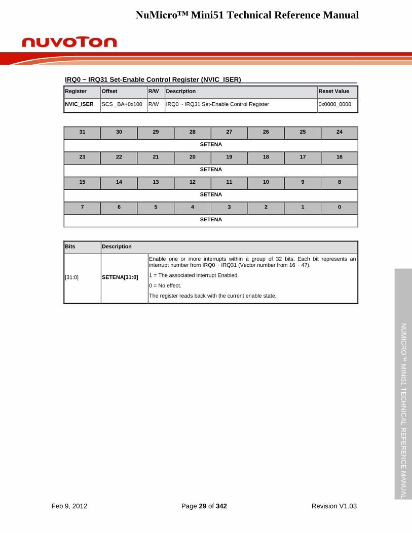
IRQ0 ~ IRQ31 Set-Enable Control Register (NVIC_ISER)
Register Offset R/W Description Reset Value
NVIC_ISER SCS _BA+0x100 R/W IRQ0 ~ IRQ31 Set-Enable Control Register 0x0000_0000
31 30 29 28 27 26 25 24
SETENA
23 22 21 20 19 18 17 16
SETENA
15 14 13 12 11 10 9 8
SETENA
7 6 5 4 3 2 1 0
SETENA
Bits Description
[31:0] SETENA[31:0]
Enable one or more interrupts within a group of 32 bits. Each bit represents an interrupt number from IRQ0 ~ IRQ31 (Vector number from 16 ~ 47).
1 = The associated interrupt Enabled.
0 = No effect.
The register reads back with the current enable state.
NuMicro™ Mini51 Technical Reference Manual
Feb 9, 2012 Page 30 of 342 Revision V1.03
NU
MIC
RO
™ M
INI5
1 T
EC
HN
ICA
L R
EF
ER
EN
CE
MA
NU
AL
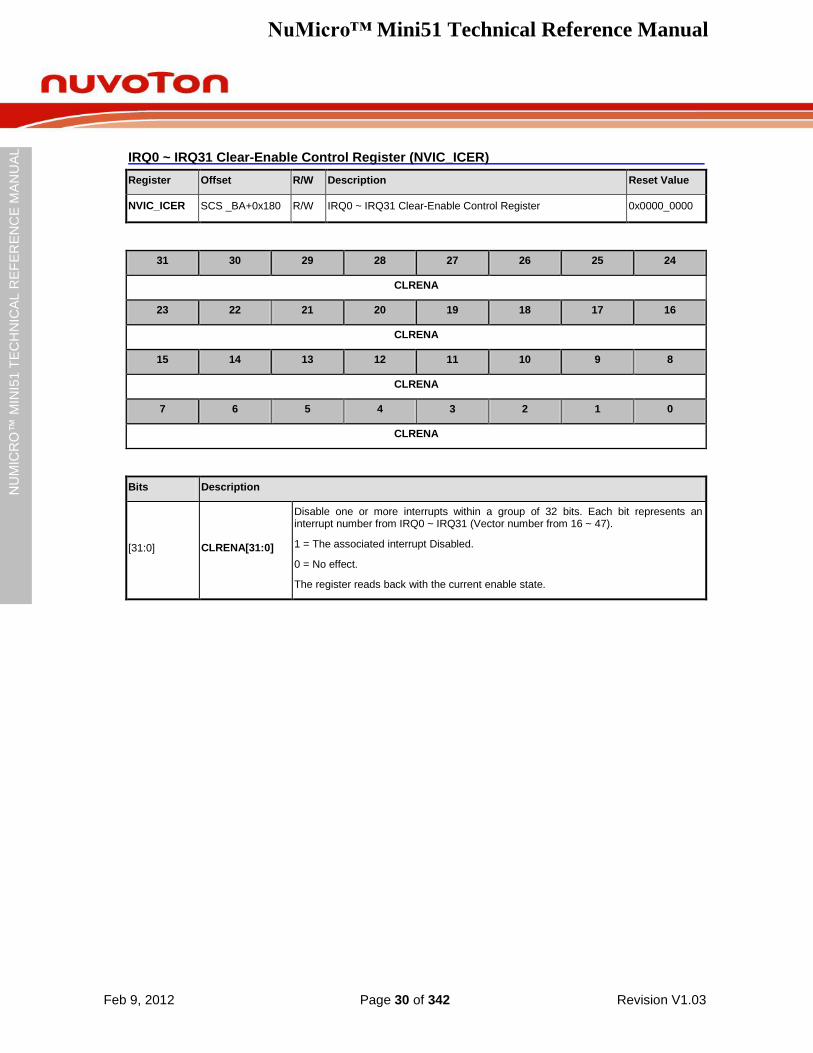
IRQ0 ~ IRQ31 Clear-Enable Control Register (NVIC_ICER)
Register Offset R/W Description Reset Value
NVIC_ICER SCS _BA+0x180 R/W IRQ0 ~ IRQ31 Clear-Enable Control Register 0x0000_0000
31 30 29 28 27 26 25 24
CLRENA
23 22 21 20 19 18 17 16
CLRENA
15 14 13 12 11 10 9 8
CLRENA
7 6 5 4 3 2 1 0
CLRENA
Bits Description
[31:0] CLRENA[31:0]
Disable one or more interrupts within a group of 32 bits. Each bit represents an interrupt number from IRQ0 ~ IRQ31 (Vector number from 16 ~ 47).
1 = The associated interrupt Disabled.
0 = No effect.
The register reads back with the current enable state.
NuMicro™ Mini51 Technical Reference Manual
Feb 9, 2012 Page 31 of 342 Revision V1.03
NU
MIC
RO
™ M
INI5
1 T
EC
HN
ICA
L R
EF
ER
EN
CE
MA
NU
AL
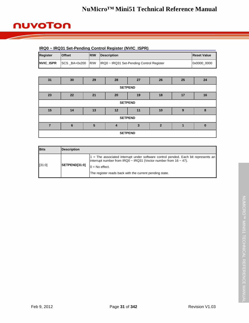
IRQ0 ~ IRQ31 Set-Pending Control Register (NVIC_ISPR)
Register Offset R/W Description Reset Value
NVIC_ISPR SCS _BA+0x200 R/W IRQ0 ~ IRQ31 Set-Pending Control Register 0x0000_0000
31 30 29 28 27 26 25 24
SETPEND
23 22 21 20 19 18 17 16
SETPEND
15 14 13 12 11 10 9 8
SETPEND
7 6 5 4 3 2 1 0
SETPEND
Bits Description
[31:0] SETPEND[31:0]
1 = The associated interrupt under software control pended. Each bit represents an interrupt number from IRQ0 ~ IRQ31 (Vector number from 16 ~ 47).
0 = No effect.
The register reads back with the current pending state.

NuMicro™ Mini51 Technical Reference Manual
Feb 9, 2012 Page 32 of 342 Revision V1.03
NU
MIC
RO
™ M
INI5
1 T
EC
HN
ICA
L R
EF
ER
EN
CE
MA
NU
AL
IRQ0 ~ IRQ31 Clear-Pending Control Register (NVIC_ICPR)
Register Offset R/W Description Reset Value
NVIC_ICPR SCS _BA+0x280 R/W IRQ0 ~ IRQ31 Clear-Pending Control Register 0x0000_0000
31 30 29 28 27 26 25 24
CLRPEND
23 22 21 20 19 18 17 16
CLRPEND
15 14 13 12 11 10 9 8
CLRPEND
7 6 5 4 3 2 1 0
CLRPEND
Bits Description
[31:0] CLRPEND[31:0]
1 = The associated interrupt under software control un-pended. Each bit represents an interrupt number from IRQ0 ~ IRQ31 (Vector number from 16 ~ 47).
0 = No effect.
The register reads back with the current pending state.

NuMicro™ Mini51 Technical Reference Manual
Feb 9, 2012 Page 33 of 342 Revision V1.03
NU
MIC
RO
™ M
INI5
1 T
EC
HN
ICA
L R
EF
ER
EN
CE
MA
NU
AL
IRQ0 ~ IRQ3 Interrupt Priority Register (NVIC_IPR0)
Register Offset R/W Description Reset Value
NVIC_IPR0 SCS _BA+0x400 R/W IRQ0 ~ IRQ3 Interrupt Priority Control Register 0x0000_0000
31 30 29 28 27 26 25 24
PRI_3 -
23 22 21 20 19 18 17 16
PRI_2 -
15 14 13 12 11 10 9 8
PRI_1 -
7 6 5 4 3 2 1 0
PRI_0 -
Bits Description
[31:30] PRI_3[1:0] Priority of IRQ3
“0” denotes the highest priority and “3” denotes the lowest priority.
[29:24] - Reserved
[23:22] PRI_2[1:0] Priority of IRQ2
“0” denotes the highest priority and “3” denotes the lowest priority.
[21:16] - Reserved
[15:14] PRI_1[1:0] Priority of IRQ1
“0” denotes the highest priority and “3” denotes the lowest priority.
[13:8] - Reserved
[7:6] PRI_0[1:0] Priority of IRQ0
“0” denotes the highest priority and “3” denotes the lowest priority.
[5:0] - Reserved
NuMicro™ Mini51 Technical Reference Manual
Feb 9, 2012 Page 34 of 342 Revision V1.03
NU
MIC
RO
™ M
INI5
1 T
EC
HN
ICA
L R
EF
ER
EN
CE
MA
NU
AL
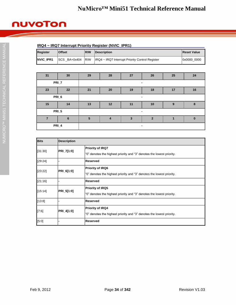
IRQ4 ~ IRQ7 Interrupt Priority Register (NVIC_IPR1)
Register Offset R/W Description Reset Value
NVIC_IPR1 SCS _BA+0x404 R/W IRQ4 ~ IRQ7 Interrupt Priority Control Register 0x0000_0000
31 30 29 28 27 26 25 24
PRI_7 -
23 22 21 20 19 18 17 16
PRI_6 -
15 14 13 12 11 10 9 8
PRI_5 -
7 6 5 4 3 2 1 0
PRI_4 -
Bits Description
[31:30] PRI_7[1:0] Priority of IRQ7
“0” denotes the highest priority and “3” denotes the lowest priority.
[29:24] - Reserved
[23:22] PRI_6[1:0] Priority of IRQ6
“0” denotes the highest priority and “3” denotes the lowest priority.
[21:16] - Reserved
[15:14] PRI_5[1:0] Priority of IRQ5
“0” denotes the highest priority and “3” denotes the lowest priority.
[13:8] - Reserved
[7:6] PRI_4[1:0] Priority of IRQ4
“0” denotes the highest priority and “3” denotes the lowest priority.
[5:0] - Reserved

NuMicro™ Mini51 Technical Reference Manual
Feb 9, 2012 Page 35 of 342 Revision V1.03
NU
MIC
RO
™ M
INI5
1 T
EC
HN
ICA
L R
EF
ER
EN
CE
MA
NU
AL
IRQ8 ~ IRQ11 Interrupt Priority Register (NVIC_IPR2)
Register Offset R/W Description Reset Value
NVIC_IPR2 SCS _BA+0x408 R/W IRQ8 ~ IRQ11 Interrupt Priority Control Register 0x0000_0000
31 30 29 28 27 26 25 24
PRI_11 -
23 22 21 20 19 18 17 16
PRI_10 -
15 14 13 12 11 10 9 8
PRI_9 -
7 6 5 4 3 2 1 0
PRI_8 -
Bits Description
[31:30] PRI_11[1:0] Priority of IRQ11
“0” denotes the highest priority and “3” denotes the lowest priority.
[29:24] - Reserved
[23:22] PRI_10[1:0] Priority of IRQ10
“0” denotes the highest priority and “3” denotes the lowest priority.
[21:16] - Reserved
[15:14] PRI_9[1:0] Priority of IRQ9
“0” denotes the highest priority and “3” denotes the lowest priority.
[13:8] - Reserved
[7:6] PRI_8[1:0] Priority of IRQ8
“0” denotes the highest priority and “3” denotes the lowest priority.
[5:0] - Reserved

NuMicro™ Mini51 Technical Reference Manual
Feb 9, 2012 Page 36 of 342 Revision V1.03
NU
MIC
RO
™ M
INI5
1 T
EC
HN
ICA
L R
EF
ER
EN
CE
MA
NU
AL
IRQ12 ~ IRQ15 Interrupt Priority Register (NVIC_IPR3)
Register Offset R/W Description Reset Value
NVIC_IPR3 SCS _BA+0x40C R/W IRQ12 ~ IRQ15 Interrupt Priority Control Register 0x0000_0000
31 30 29 28 27 26 25 24
PRI_15 -
23 22 21 20 19 18 17 16
PRI_14 -
15 14 13 12 11 10 9 8
PRI_13 -
7 6 5 4 3 2 1 0
PRI_12 -
Bits Description
[31:30] PRI_15[1:0] Priority of IRQ15
“0” denotes the highest priority and “3” denotes the lowest priority.
[29:24] - Reserved
[23:22] PRI_14[1:0] Priority of IRQ14
“0” denotes the highest priority and “3” denotes the lowest priority.
[21:16] - Reserved
[15:14] PRI_13[1:0] Priority of IRQ13
“0” denotes the highest priority and “3” denotes the lowest priority.
[13:8] - Reserved
[7:6] PRI_12[1:0] Priority of IRQ12
“0” denotes the highest priority and “3” denotes the lowest priority.
[5:0] - Reserved
NuMicro™ Mini51 Technical Reference Manual
Feb 9, 2012 Page 37 of 342 Revision V1.03
NU
MIC
RO
™ M
INI5
1 T
EC
HN
ICA
L R
EF
ER
EN
CE
MA
NU
AL
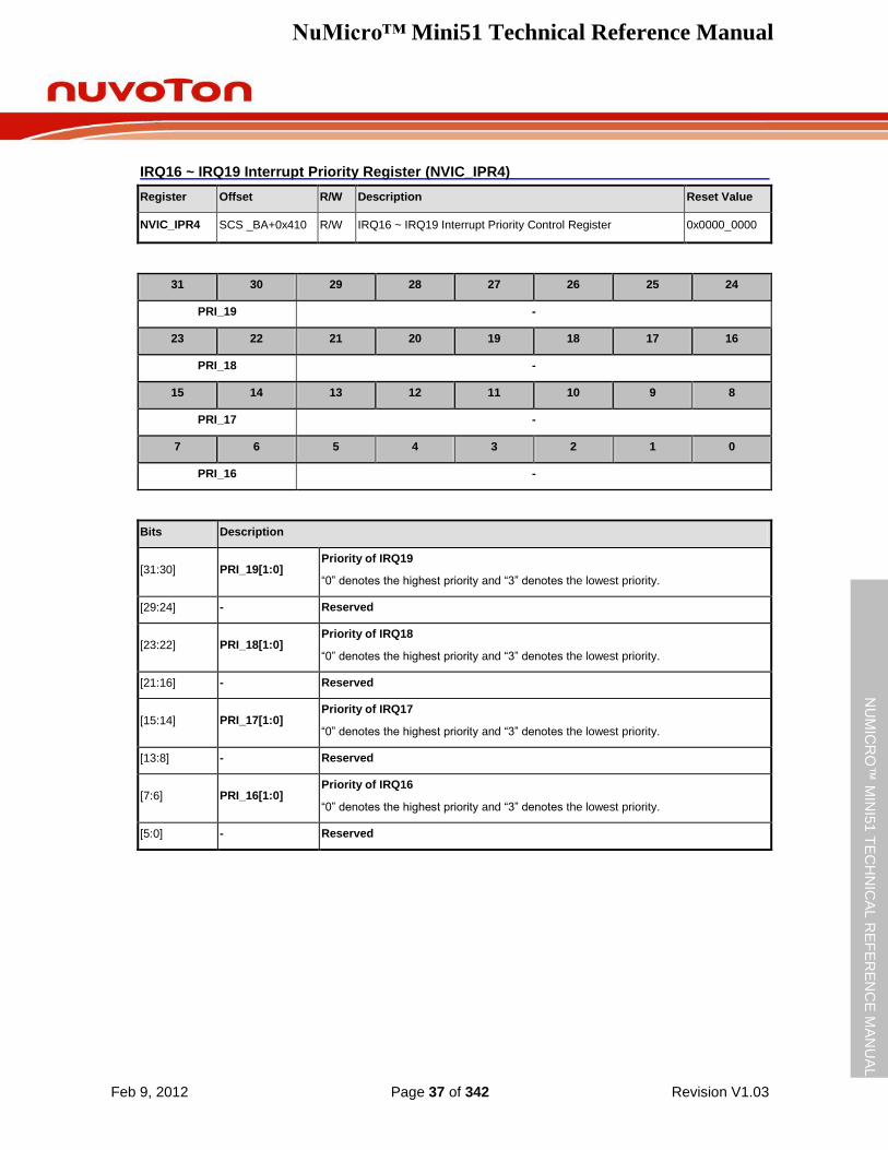
IRQ16 ~ IRQ19 Interrupt Priority Register (NVIC_IPR4)
Register Offset R/W Description Reset Value
NVIC_IPR4 SCS _BA+0x410 R/W IRQ16 ~ IRQ19 Interrupt Priority Control Register 0x0000_0000
31 30 29 28 27 26 25 24
PRI_19 -
23 22 21 20 19 18 17 16
PRI_18 -
15 14 13 12 11 10 9 8
PRI_17 -
7 6 5 4 3 2 1 0
PRI_16 -
Bits Description
[31:30] PRI_19[1:0] Priority of IRQ19
“0” denotes the highest priority and “3” denotes the lowest priority.
[29:24] - Reserved
[23:22] PRI_18[1:0] Priority of IRQ18
“0” denotes the highest priority and “3” denotes the lowest priority.
[21:16] - Reserved
[15:14] PRI_17[1:0] Priority of IRQ17
“0” denotes the highest priority and “3” denotes the lowest priority.
[13:8] - Reserved
[7:6] PRI_16[1:0] Priority of IRQ16
“0” denotes the highest priority and “3” denotes the lowest priority.
[5:0] - Reserved

NuMicro™ Mini51 Technical Reference Manual
Feb 9, 2012 Page 38 of 342 Revision V1.03
NU
MIC
RO
™ M
INI5
1 T
EC
HN
ICA
L R
EF
ER
EN
CE
MA
NU
AL
IRQ20 ~ IRQ23 Interrupt Priority Register (NVIC_IPR5)
Register Offset R/W Description Reset Value
NVIC_IPR5 SCS _BA+0x414 R/W IRQ20 ~ IRQ23 Interrupt Priority Control Register 0x0000_0000
31 30 29 28 27 26 25 24
PRI_23 -
23 22 21 20 19 18 17 16
PRI_22 -
15 14 13 12 11 10 9 8
PRI_21 -
7 6 5 4 3 2 1 0
PRI_20 -
Bits Description
[31:30] PRI_23[1:0] Priority of IRQ23
“0” denotes the highest priority and “3” denotes the lowest priority.
[29:24] - Reserved
[23:22] PRI_22[1:0] Priority of IRQ22
“0” denotes the highest priority and “3” denotes the lowest priority.
[21:16] - Reserved
[15:14] PRI_21[1:0] Priority of IRQ21
“0” denotes the highest priority and “3” denotes the lowest priority.
[13:8] - Reserved
[7:6] PRI_20[1:0] Priority of IRQ20
“0” denotes the highest priority and “3” denotes the lowest priority.
[5:0] - Reserved

NuMicro™ Mini51 Technical Reference Manual
Feb 9, 2012 Page 39 of 342 Revision V1.03
NU
MIC
RO
™ M
INI5
1 T
EC
HN
ICA
L R
EF
ER
EN
CE
MA
NU
AL
IRQ24 ~ IRQ27 Interrupt Priority Register (NVIC_IPR6)
Register Offset R/W Description Reset Value
NVIC_IPR6 SCS _BA+0x418 R/W IRQ24 ~ IRQ27 Interrupt Priority Control Register 0x0000_0000
31 30 29 28 27 26 25 24
PRI_27 -
23 22 21 20 19 18 17 16
PRI_26 -
15 14 13 12 11 10 9 8
PRI_25 -
7 6 5 4 3 2 1 0
PRI_24 -
Bits Description
[31:30] PRI_27[1:0] Priority of IRQ27
“0” denotes the highest priority and “3” denotes the lowest priority.
[29:24] - Reserved
[23:22] PRI_26[1:0] Priority of IRQ26
“0” denotes the highest priority and “3” denotes the lowest priority.
[21:16] - Reserved
[15:14] PRI_25[1:0] Priority of IRQ25
“0” denotes the highest priority and “3” denotes the lowest priority.
[13:8] - Reserved
[7:6] PRI_24[1:0] Priority of IRQ24
“0” denotes the highest priority and “3” denotes the lowest priority.
[5:0] - Reserved
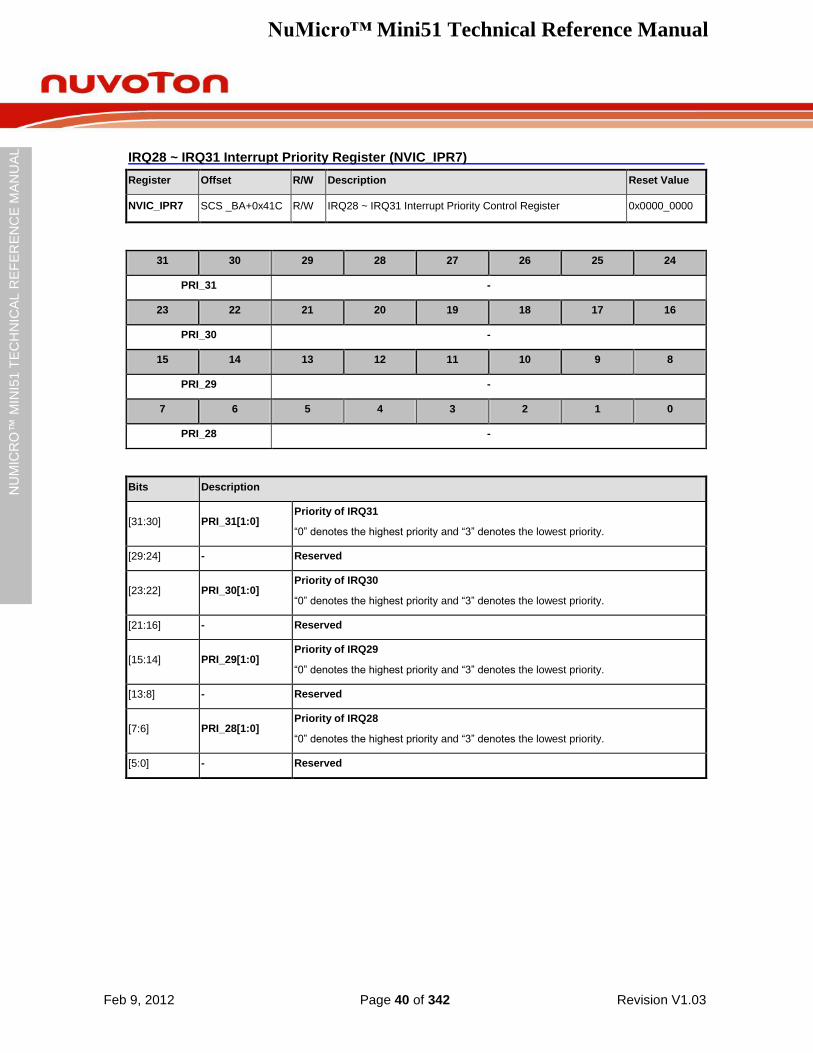
NuMicro™ Mini51 Technical Reference Manual
Feb 9, 2012 Page 40 of 342 Revision V1.03
NU
MIC
RO
™ M
INI5
1 T
EC
HN
ICA
L R
EF
ER
EN
CE
MA
NU
AL
IRQ28 ~ IRQ31 Interrupt Priority Register (NVIC_IPR7)
Register Offset R/W Description Reset Value
NVIC_IPR7 SCS _BA+0x41C R/W IRQ28 ~ IRQ31 Interrupt Priority Control Register 0x0000_0000
31 30 29 28 27 26 25 24
PRI_31 -
23 22 21 20 19 18 17 16
PRI_30 -
15 14 13 12 11 10 9 8
PRI_29 -
7 6 5 4 3 2 1 0
PRI_28 -
Bits Description
[31:30] PRI_31[1:0] Priority of IRQ31
“0” denotes the highest priority and “3” denotes the lowest priority.
[29:24] - Reserved
[23:22] PRI_30[1:0] Priority of IRQ30
“0” denotes the highest priority and “3” denotes the lowest priority.
[21:16] - Reserved
[15:14] PRI_29[1:0] Priority of IRQ29
“0” denotes the highest priority and “3” denotes the lowest priority.
[13:8] - Reserved
[7:6] PRI_28[1:0] Priority of IRQ28
“0” denotes the highest priority and “3” denotes the lowest priority.
[5:0] - Reserved
NuMicro™ Mini51 Technical Reference Manual
Feb 9, 2012 Page 41 of 342 Revision V1.03
NU
MIC
RO
™ M
INI5
1 T
EC
HN
ICA
L R
EF
ER
EN
CE
MA
NU
AL
5.2.7 Interrupt Source Control Registers
Besides the interrupt control registers associated with the NVIC, the NuMicro Mini51 series also implements some specific control registers to facilitate the interrupt functions, including “interrupt source identify”, ”NMI source selection” and “interrupt test mode”, which are described below.
R: read only, W: write only, R/W: both read and write
Register Offset R/W Description Reset Value
INT_BA = 0x5000_0300
IRQ0_SRC INT_BA+0x00 R IRQ0 (Brown-out) Interrupt Source Identity 0xXXXX_XXXX
IRQ1_SRC INT_BA+0x04 R IRQ1 (WDT) Interrupt Source Identity 0xXXXX_XXXX
IRQ2_SRC INT_BA+0x08 R IRQ2 (EINT0) Interrupt Source Identity 0xXXXX_XXXX
IRQ3_SRC INT_BA+0x0C R IRQ3 (EINT1) Interrupt Source Identity 0xXXXX_XXXX
IRQ4_SRC INT_BA+0x10 R IRQ4 (GP0/1) Interrupt Source Identity 0xXXXX_XXXX
IRQ5_SRC INT_BA+0x14 R IRQ5 (GP2/3/4) Interrupt Source Identity 0xXXXX_XXXX
IRQ6_SRC INT_BA+0x18 R IRQ6 (PWM) Interrupt Source Identity 0xXXXX_XXXX
IRQ7_SRC INT_BA+0x1C R IRQ7 (BRAKE) Interrupt Source Identity 0xXXXX_XXXX
IRQ8_SRC INT_BA+0x20 R IRQ8 (TMR0) Interrupt Source Identity 0xXXXX_XXXX
IRQ9_SRC INT_BA+0x24 R IRQ9 (TMR1) Interrupt Source Identity 0xXXXX_XXXX
IRQ10_SRC INT_BA+0x28 - Reserved 0xXXXX_XXXX
IRQ11_SRC INT_BA+0x2C - Reserved 0xXXXX_XXXX
IRQ12_SRC INT_BA+0x30 R IRQ12 (UART) Interrupt Source Identity 0xXXXX_XXXX
IRQ13_SRC INT_BA+0x34 - Reserved 0xXXXX_XXXX
IRQ14_SRC INT_BA+0x38 R IRQ14 (SPI) Interrupt Source Identity 0xXXXX_XXXX
IRQ15_SRC INT_BA+0x3C - Reserved 0xXXXX_XXXX
IRQ16_SRC INT_BA+0x40 R IRQ16 (GP5) Interrupt Source Identity 0xXXXX_XXXX
IRQ17_SRC INT_BA+0x44 R IRQ17 (HFIRC trim) Interrupt Source Identity 0xXXXX_XXXX
IRQ18_SRC INT_BA+0x48 R IRQ18 (I2C) Interrupt Source Identity 0xXXXX_XXXX
IRQ19_SRC INT_BA+0x4C - Reserved 0xXXXX_XXXX
IRQ20_SRC INT_BA+0x50 - Reserved 0xXXXX_XXXX
IRQ21_SRC INT_BA+0x54 - Reserved 0xXXXX_XXXX
IRQ22_SRC INT_BA+0x58 - Reserved 0xXXXX_XXXX
IRQ23_SRC INT_BA+0x5C - Reserved 0xXXXX_XXXX
NuMicro™ Mini51 Technical Reference Manual
Feb 9, 2012 Page 42 of 342 Revision V1.03
NU
MIC
RO
™ M
INI5
1 T
EC
HN
ICA
L R
EF
ER
EN
CE
MA
NU
AL
Register Offset R/W Description Reset Value
INT_BA = 0x5000_0300
IRQ24_SRC INT_BA+0x60 - Reserved 0xXXXX_XXXX
IRQ25_SRC INT_BA+0x64 R IRQ25 (ACMP) Interrupt Source Identity 0xXXXX_XXXX
IRQ26_SRC INT_BA+0x68 - Reserved 0xXXXX_XXXX
IRQ27_SRC INT_BA+0x6C - Reserved 0xXXXX_XXXX
IRQ28_SRC INT_BA+0x70 R IRQ28 (PWRWU) Interrupt Source Identity 0xXXXX_XXXX
IRQ29_SRC INT_BA+0x74 R IRQ29 (ADC) Interrupt Source Identity 0xXXXX_XXXX
IRQ30_SRC INT_BA+0x78 - Reserved 0xXXXX_XXXX
IRQ31_SRC INT_BA+0x7C - Reserved 0xXXXX_XXXX
NMI_CON INT_BA+0x80 R/W NMI Source Interrupt Select Control Register 0x0000_0000
MCU_IRQ INT_BA+0x84 R/W MCU IRQ Number Identity Register 0x0000_0000
NuMicro™ Mini51 Technical Reference Manual
Feb 9, 2012 Page 43 of 342 Revision V1.03
NU
MIC
RO
™ M
INI5
1 T
EC
HN
ICA
L R
EF
ER
EN
CE
MA
NU
AL
Interrupt Source Identify Register (IRQn_SRC)
Register Offset R/W Description Reset Value
IRQn_SRC
INT_BA+0x00
……..
INT_BA+0x7C
R
MCU IRQ0 (BOD) Interrupt Source Identity
:
MCU IRQ31 (Reserved) Interrupt Source Identity
0xXXXX_XXXX
31 30 29 28 27 26 25 24
-
23 22 21 20 19 18 17 16
-
15 14 13 12 11 10 9 8
-
7 6 5 4 3 2 1 0
- INT_SRC
Bits Address IRQ No. Description
[31:3] - - Reserved.
[2:0] INT_BA+0x00 0 Bit1~2: Reserved
Bit0: BOD_INT
[2:0] INT_BA+0x04 1 Bit1~2: Reserved
Bit0: WDT_INT
[2:0] INT_BA+0x08 2 Bit1~2: Reserved
Bit0: EINT0 – external interrupt 0 from P3.2.
[2:0] INT_BA+0x0C 3 Bit1~2: Reserved
Bit0: EINT1 – external interrupt 1 from P5.2.
[2:0] INT_BA+0x10 4
Bit2: Reserved
Bit1: P1_INT
Bit0: P0_INT
[2:0] INT_BA+0x14 5
Bit2: P4_INT
Bit1: P3_INT
Bit0: P2_INT
[2:0] INT_BA+0x18 6 Bit1~2: Reserved
Bit0: PWM_INT
[2:0] INT_BA+0x1C 7 Bit1~2: Reserved
Bit0: BRAKE_INT
NuMicro™ Mini51 Technical Reference Manual
Feb 9, 2012 Page 44 of 342 Revision V1.03
NU
MIC
RO
™ M
INI5
1 T
EC
HN
ICA
L R
EF
ER
EN
CE
MA
NU
AL
Bits Address IRQ No. Description
[2:0] INT_BA+0x20 8 Bit1~2: Reserved
Bit0: TMR0_INT
[2:0] INT_BA+0x24 9 Bit1~2: Reserved
Bit0: TMR1_INT
[2:0] INT_BA+0x28 10 Reserved
[2:0] INT_BA+0x2C 11 Reserved
[2:0] INT_BA+0x30 12 Bit1~2: Reserved
Bit0: UART_INT
[2:0] INT_BA+0x34 13 Reserved
[2:0] INT_BA+0x38 14 Bit1~2: Reserved
Bit0: SPI_INT
[2:0] INT_BA+0x3C 15 Reserved
[2:0] INT_BA+0x40 16 Bit1~2: Reserved
Bit0: P5_INT
[2:0] INT_BA+0x44 17 Bit1~2: Reserved
Bit0: HFIRC_TRIM_INT
[2:0] INT_BA+0x48 18 Bit1~2: Reserved
Bit0: I2C_INT
[2:0] INT_BA+0x4C 19 Reserved.
[2:0] INT_BA+0x50 20 Reserved
[2:0] INT_BA+0x54 21 Reserved
[2:0] INT_BA+0x58 22 Reserved
[2:0] INT_BA+0x5C 23 Reserved
[2:0] INT_BA+0x60 24 Reserved
[2:0] INT_BA+0x64 25 Bit1~2: Reserved
Bit0: ACMP_INT
[2:0] INT_BA+0x68 26 Reserved
[2:0] INT_BA+0x6C 27 Reserved
[2:0] INT_BA+0x70 28 Bit1~2: Reserved
Bit0: PWRWU_INT
[2:0] INT_BA+0x74 29 Bit1~2: Reserved
Bit0: ADC_INT
[2:0] INT_BA+0x78 30 Reserved
[2:0] INT_BA+0x7C 31 Reserved
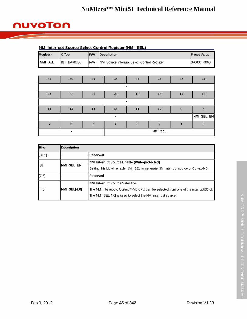
NuMicro™ Mini51 Technical Reference Manual
Feb 9, 2012 Page 45 of 342 Revision V1.03
NU
MIC
RO
™ M
INI5
1 T
EC
HN
ICA
L R
EF
ER
EN
CE
MA
NU
AL
NMI Interrupt Source Select Control Register (NMI_SEL)
Register Offset R/W Description Reset Value
NMI_SEL INT_BA+0x80 R/W NMI Source Interrupt Select Control Register 0x0000_0000
31 30 29 28 27 26 25 24
-
23 22 21 20 19 18 17 16
-
15 14 13 12 11 10 9 8
- NMI_SEL_EN
7 6 5 4 3 2 1 0
- NMI_SEL
Bits Description
[31:9] - Reserved
[8] NMI_SEL_EN NMI Interrupt Source Enable (Write-protected)
Setting this bit will enable NMI_SEL to generate NMI interrupt source of Cortex-M0.
[7:5] - Reserved
[4:0] NMI_SEL[4:0]
NMI Interrupt Source Selection
The NMI interrupt to Cortex™-M0 CPU can be selected from one of the interrupt[31:0].
The NMI_SEL[4:0] is used to select the NMI interrupt source.
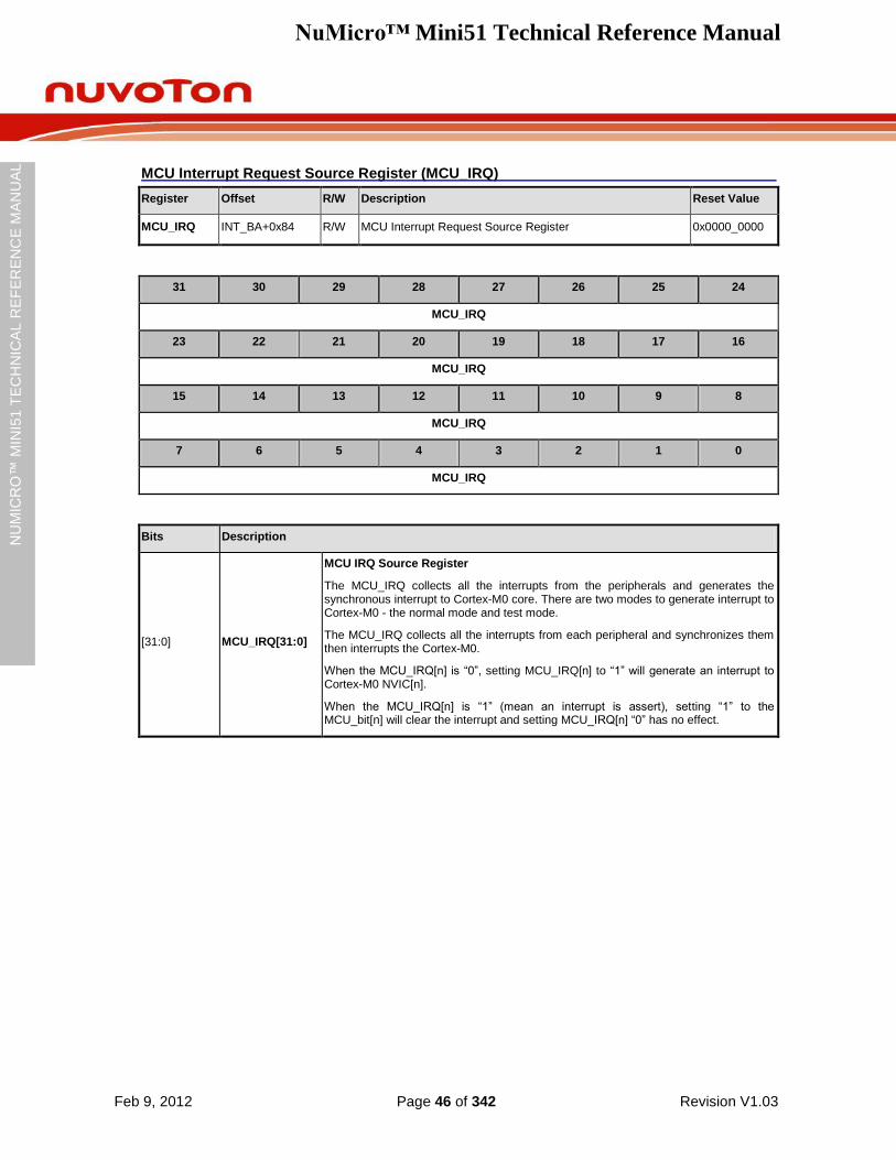
NuMicro™ Mini51 Technical Reference Manual
Feb 9, 2012 Page 46 of 342 Revision V1.03
NU
MIC
RO
™ M
INI5
1 T
EC
HN
ICA
L R
EF
ER
EN
CE
MA
NU
AL
MCU Interrupt Request Source Register (MCU_IRQ)
Register Offset R/W Description Reset Value
MCU_IRQ INT_BA+0x84 R/W MCU Interrupt Request Source Register 0x0000_0000
31 30 29 28 27 26 25 24
MCU_IRQ
23 22 21 20 19 18 17 16
MCU_IRQ
15 14 13 12 11 10 9 8
MCU_IRQ
7 6 5 4 3 2 1 0
MCU_IRQ
Bits Description
[31:0] MCU_IRQ[31:0]
MCU IRQ Source Register
The MCU_IRQ collects all the interrupts from the peripherals and generates the synchronous interrupt to Cortex-M0 core. There are two modes to generate interrupt to Cortex-M0 - the normal mode and test mode.
The MCU_IRQ collects all the interrupts from each peripheral and synchronizes them then interrupts the Cortex-M0.
When the MCU_IRQ[n] is “0”, setting MCU_IRQ[n] to “1” will generate an interrupt to Cortex-M0 NVIC[n].
When the MCU_IRQ[n] is “1” (mean an interrupt is assert), setting “1” to the MCU_bit[n] will clear the interrupt and setting MCU_IRQ[n] “0” has no effect.
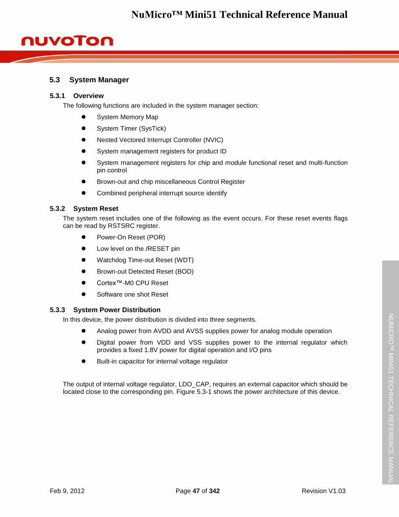
NuMicro™ Mini51 Technical Reference Manual
Feb 9, 2012 Page 47 of 342 Revision V1.03
NU
MIC
RO
™ M
INI5
1 T
EC
HN
ICA
L R
EF
ER
EN
CE
MA
NU
AL
5.3 System Manager
5.3.1 Overview
The following functions are included in the system manager section:
System Memory Map
System Timer (SysTick)
Nested Vectored Interrupt Controller (NVIC)
System management registers for product ID
System management registers for chip and module functional reset and multi-function pin control
Brown-out and chip miscellaneous Control Register
Combined peripheral interrupt source identify
5.3.2 System Reset
The system reset includes one of the following as the event occurs. For these reset events flags can be read by RSTSRC register.
Power-On Reset (POR)
Low level on the /RESET pin
Watchdog Time-out Reset (WDT)
Brown-out Detected Reset (BOD)
Cortex™-M0 CPU Reset
Software one shot Reset
5.3.3 System Power Distribution
In this device, the power distribution is divided into three segments.
Analog power from AVDD and AVSS supplies power for analog module operation
Digital power from VDD and VSS supplies power to the internal regulator which provides a fixed 1.8V power for digital operation and I/O pins
Built-in capacitor for internal voltage regulator
The output of internal voltage regulator, LDO_CAP, requires an external capacitor which should be located close to the corresponding pin. Figure 5.3-1 shows the power architecture of this device.
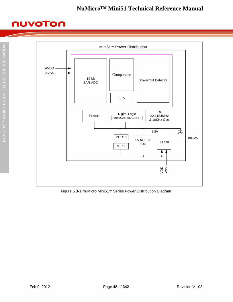
NuMicro™ Mini51 Technical Reference Manual
Feb 9, 2012 Page 48 of 342 Revision V1.03
NU
MIC
RO
™ M
INI5
1 T
EC
HN
ICA
L R
EF
ER
EN
CE
MA
NU
AL
Brown Out Detector
POR50
FLASHDigital Logic
(Timer/UART/I2C/SPI…)
1.8V
IRC
22.1184MHz
& 10KHz Osc.
AVDD
AVSS
VD
D
VS
S
IO cell
P0~P5
10-bit
SAR-ADC
POR185V to 1.8V
LDO
Comparator
CRV
Mini51™ Power Distribution
Figure 5.3-1 NuMicro Mini51 Series Power Distribution Diagram
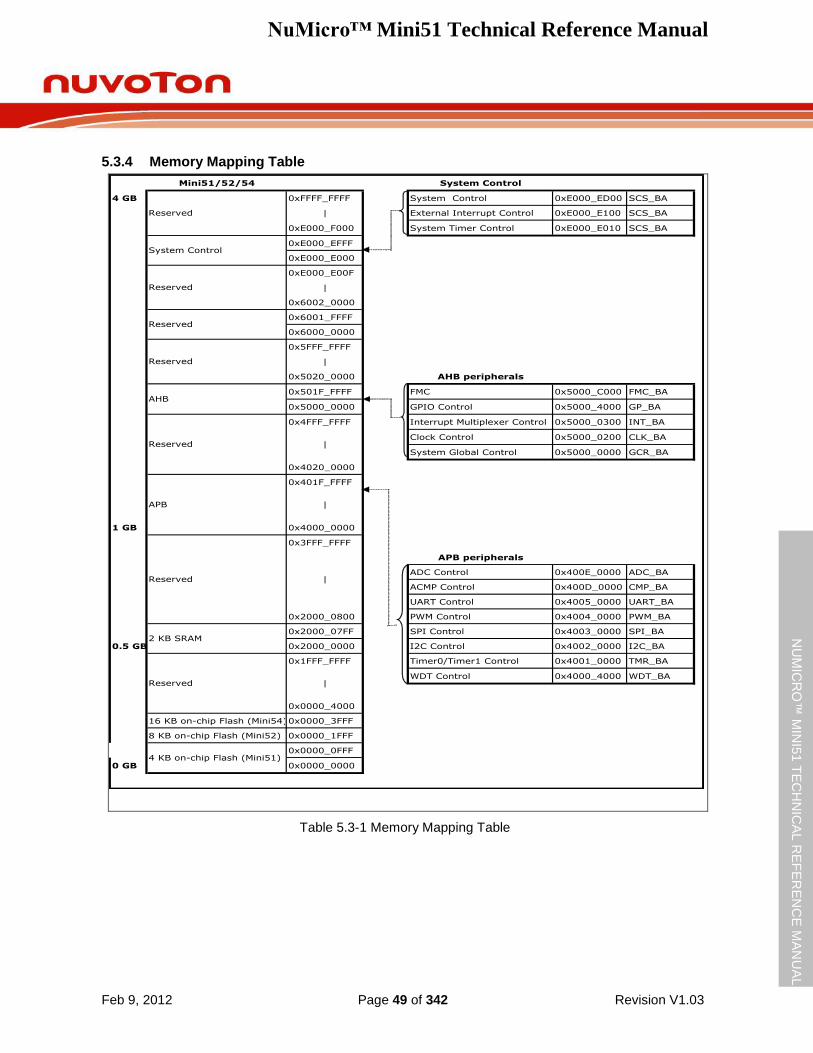
NuMicro™ Mini51 Technical Reference Manual
Feb 9, 2012 Page 49 of 342 Revision V1.03
NU
MIC
RO
™ M
INI5
1 T
EC
HN
ICA
L R
EF
ER
EN
CE
MA
NU
AL
5.3.4 Memory Mapping Table
Table 5.3-1 Memory Mapping Table
Mini51/52/54 System Control
4 GB 0xFFFF_FFFF System Control 0xE000_ED00 SCS_BA
| External Interrupt Control 0xE000_E100 SCS_BA
0xE000_F000 System Timer Control 0xE000_E010 SCS_BA
0xE000_EFFF
0xE000_E000
0xE000_E00F
|
0x6002_0000
0x6001_FFFF
0x6000_0000
0x5FFF_FFFF
|
0x5020_0000 AHB peripherals
0x501F_FFFF FMC 0x5000_C000 FMC_BA
0x5000_0000 GPIO Control 0x5000_4000 GP_BA
0x4FFF_FFFF Interrupt Multiplexer Control 0x5000_0300 INT_BA
Clock Control 0x5000_0200 CLK_BA
System Global Control 0x5000_0000 GCR_BA
0x4020_0000
0x401F_FFFF
1 GB 0x4000_0000
0x3FFF_FFFF
APB peripherals
ADC Control 0x400E_0000 ADC_BA
ACMP Control 0x400D_0000 CMP_BA
UART Control 0x4005_0000 UART_BA
0x2000_0800 PWM Control 0x4004_0000 PWM_BA
0x2000_07FF SPI Control 0x4003_0000 SPI_BA
0.5 GB 0x2000_0000 I2C Control 0x4002_0000 I2C_BA
0x1FFF_FFFF Timer0/Timer1 Control 0x4001_0000 TMR_BA
WDT Control 0x4000_4000 WDT_BA
0x0000_4000
16 KB on-chip Flash (Mini54)0x0000_3FFF
8 KB on-chip Flash (Mini52) 0x0000_1FFF
0x0000_0FFF
0 GB 0x0000_0000
|
|
|
|
System Control
Reserved
4 KB on-chip Flash (Mini51)
2 KB SRAM
Reserved
Reserved
Reserved
Reserved
APB
Reserved
AHB
Reserved
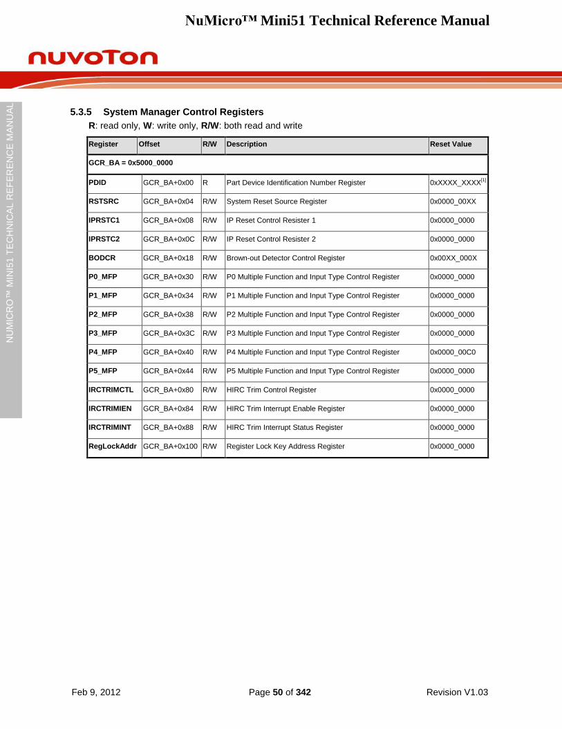
NuMicro™ Mini51 Technical Reference Manual
Feb 9, 2012 Page 50 of 342 Revision V1.03
NU
MIC
RO
™ M
INI5
1 T
EC
HN
ICA
L R
EF
ER
EN
CE
MA
NU
AL
5.3.5 System Manager Control Registers
R: read only, W: write only, R/W: both read and write
Register Offset R/W Description Reset Value
GCR_BA = 0x5000_0000
PDID GCR_BA+0x00 R Part Device Identification Number Register 0xXXXX_XXXX[1]
RSTSRC GCR_BA+0x04 R/W System Reset Source Register 0x0000_00XX
IPRSTC1 GCR_BA+0x08 R/W IP Reset Control Resister 1 0x0000_0000
IPRSTC2 GCR_BA+0x0C R/W IP Reset Control Resister 2 0x0000_0000
BODCR GCR_BA+0x18 R/W Brown-out Detector Control Register 0x00XX_000X
P0_MFP GCR_BA+0x30 R/W P0 Multiple Function and Input Type Control Register 0x0000_0000
P1_MFP GCR_BA+0x34 R/W P1 Multiple Function and Input Type Control Register 0x0000_0000
P2_MFP GCR_BA+0x38 R/W P2 Multiple Function and Input Type Control Register 0x0000_0000
P3_MFP GCR_BA+0x3C R/W P3 Multiple Function and Input Type Control Register 0x0000_0000
P4_MFP GCR_BA+0x40 R/W P4 Multiple Function and Input Type Control Register 0x0000_00C0
P5_MFP GCR_BA+0x44 R/W P5 Multiple Function and Input Type Control Register 0x0000_0000
IRCTRIMCTL GCR_BA+0x80 R/W HIRC Trim Control Register 0x0000_0000
IRCTRIMIEN GCR_BA+0x84 R/W HIRC Trim Interrupt Enable Register 0x0000_0000
IRCTRIMINT GCR_BA+0x88 R/W HIRC Trim Interrupt Status Register 0x0000_0000
RegLockAddr GCR_BA+0x100 R/W Register Lock Key Address Register 0x0000_0000
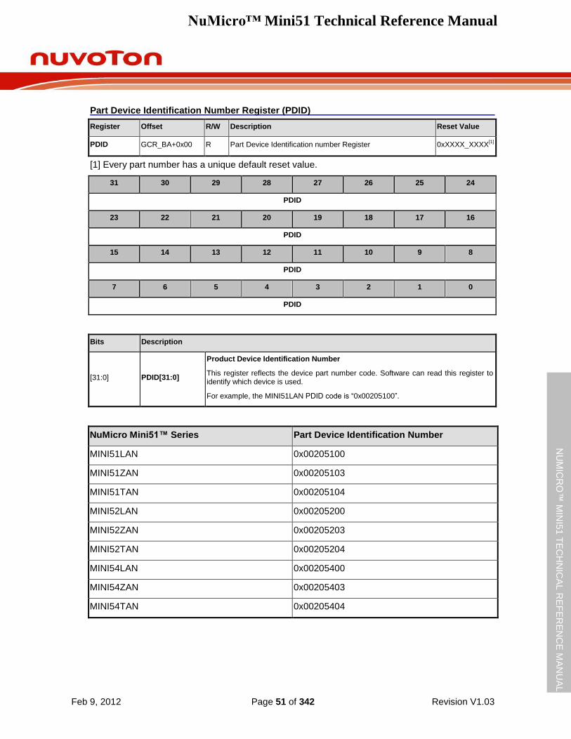
NuMicro™ Mini51 Technical Reference Manual
Feb 9, 2012 Page 51 of 342 Revision V1.03
NU
MIC
RO
™ M
INI5
1 T
EC
HN
ICA
L R
EF
ER
EN
CE
MA
NU
AL
Part Device Identification Number Register (PDID)
Register Offset R/W Description Reset Value
PDID GCR_BA+0x00 R Part Device Identification number Register 0xXXXX_XXXX[1]
[1] Every part number has a unique default reset value.
31 30 29 28 27 26 25 24
PDID
23 22 21 20 19 18 17 16
PDID
15 14 13 12 11 10 9 8
PDID
7 6 5 4 3 2 1 0
PDID
Bits Description
[31:0] PDID[31:0]
Product Device Identification Number
This register reflects the device part number code. Software can read this register to identify which device is used.
For example, the MINI51LAN PDID code is “0x00205100”.
NuMicro Mini51™ Series Part Device Identification Number
MINI51LAN 0x00205100
MINI51ZAN 0x00205103
MINI51TAN 0x00205104
MINI52LAN 0x00205200
MINI52ZAN 0x00205203
MINI52TAN 0x00205204
MINI54LAN 0x00205400
MINI54ZAN 0x00205403
MINI54TAN 0x00205404

NuMicro™ Mini51 Technical Reference Manual
Feb 9, 2012 Page 52 of 342 Revision V1.03
NU
MIC
RO
™ M
INI5
1 T
EC
HN
ICA
L R
EF
ER
EN
CE
MA
NU
AL
System Reset Source Register (RSTSRC)
This register provides specific information for software to identify the chip‟s reset source from the last operation.
Register Offset R/W Description Reset Value
RSTSRC GCR_BA+0x04 R/W System Reset Source Register 0x0000_00XX
31 30 29 28 27 26 25 24
-
23 22 21 20 19 18 17 16
-
15 14 13 12 11 10 9 8
-
7 6 5 4 3 2 1 0
RSTS_CPU - RSTS_MCU RSTS_BOD - RSTS_WDT RSTS_RESET RSTS_POR
Bits Description
[31:8] - Reserved
[7] RSTS_CPU
The RSTS_CPU flag is set by hardware if software writes CPU_RST (IPRSTC1[1]) with ”1” to reset the Cortex™-M0 CPU kernel and Flash Memory Controller (FMC).
1 = The Cortex™-M0 CPU kernel and FMC are reset by setting CPU_RST to “1”.
0 = No reset from CPU.
Software can write “1” to clear this bit to zero.
[6] - Reserved
[5] RSTS_MCU
The RSTS_MCU flag is set by the “reset signal” from the Cortex-M0 kernel to indicate the previous reset source.
1 = The Cortex-M0 had issued the reset signal to reset the system by software writing “1” to bit SYSRESETREQ (AIRCR[2]), Application Interrupt and Reset Control Register, address = 0xE000ED0C) in system control registers of Cortex-M0 kernel.
0 = No reset from the Cortex-M0.
Software can write “1” to clear this bit to zero.
[4] RSTS_BOD
The RSTS_BOD flag is set by the “reset signal” from the Brown-out-Detected module to indicate the previous reset source.
1 = The Brown-out-Detected module had issued the reset signal to reset the system.
0 = No reset from BOD.
Software can write “1” to clear this bit to zero.
[3] - Reserved
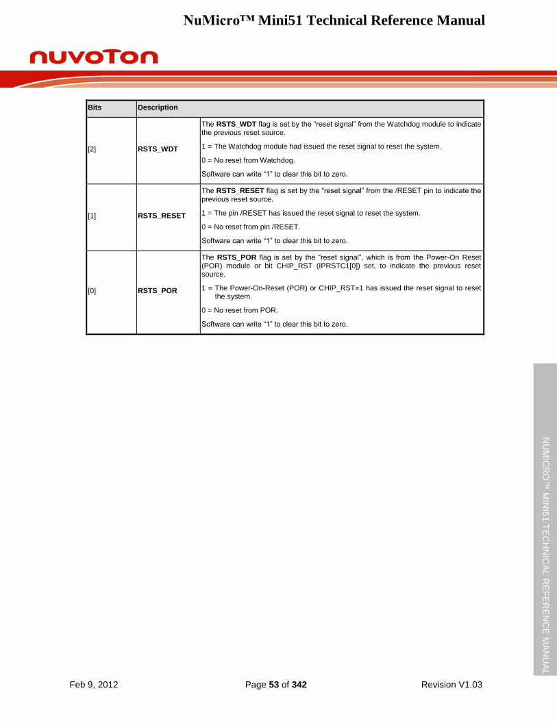
NuMicro™ Mini51 Technical Reference Manual
Feb 9, 2012 Page 53 of 342 Revision V1.03
NU
MIC
RO
™ M
INI5
1 T
EC
HN
ICA
L R
EF
ER
EN
CE
MA
NU
AL
Bits Description
[2] RSTS_WDT
The RSTS_WDT flag is set by the “reset signal” from the Watchdog module to indicate the previous reset source.
1 = The Watchdog module had issued the reset signal to reset the system.
0 = No reset from Watchdog.
Software can write “1” to clear this bit to zero.
[1] RSTS_RESET
The RSTS_RESET flag is set by the “reset signal” from the /RESET pin to indicate the previous reset source.
1 = The pin /RESET has issued the reset signal to reset the system.
0 = No reset from pin /RESET.
Software can write “1” to clear this bit to zero.
[0] RSTS_POR
The RSTS_POR flag is set by the “reset signal”, which is from the Power-On Reset (POR) module or bit CHIP_RST (IPRSTC1[0]) set, to indicate the previous reset source.
1 = The Power-On-Reset (POR) or CHIP_RST=1 has issued the reset signal to reset the system.
0 = No reset from POR.
Software can write “1” to clear this bit to zero.
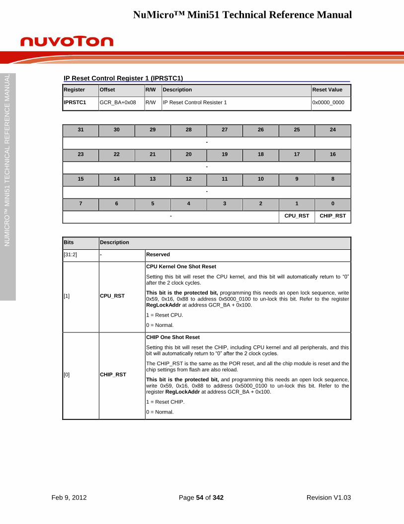
NuMicro™ Mini51 Technical Reference Manual
Feb 9, 2012 Page 54 of 342 Revision V1.03
NU
MIC
RO
™ M
INI5
1 T
EC
HN
ICA
L R
EF
ER
EN
CE
MA
NU
AL
IP Reset Control Register 1 (IPRSTC1)
Register Offset R/W Description Reset Value
IPRSTC1 GCR_BA+0x08 R/W IP Reset Control Resister 1 0x0000_0000
31 30 29 28 27 26 25 24
-
23 22 21 20 19 18 17 16
-
15 14 13 12 11 10 9 8
-
7 6 5 4 3 2 1 0
- CPU_RST CHIP_RST
Bits Description
[31:2] - Reserved
[1] CPU_RST
CPU Kernel One Shot Reset
Setting this bit will reset the CPU kernel, and this bit will automatically return to “0” after the 2 clock cycles.
This bit is the protected bit, programming this needs an open lock sequence, write 0x59, 0x16, 0x88 to address 0x5000_0100 to un-lock this bit. Refer to the register RegLockAddr at address GCR_BA + 0x100.
1 = Reset CPU.
0 = Normal.
[0] CHIP_RST
CHIP One Shot Reset
Setting this bit will reset the CHIP, including CPU kernel and all peripherals, and this bit will automatically return to “0” after the 2 clock cycles.
The CHIP_RST is the same as the POR reset, and all the chip module is reset and the chip settings from flash are also reload.
This bit is the protected bit, and programming this needs an open lock sequence, write 0x59, 0x16, 0x88 to address 0x5000_0100 to un-lock this bit. Refer to the register RegLockAddr at address GCR_BA + 0x100.
1 = Reset CHIP.
0 = Normal.
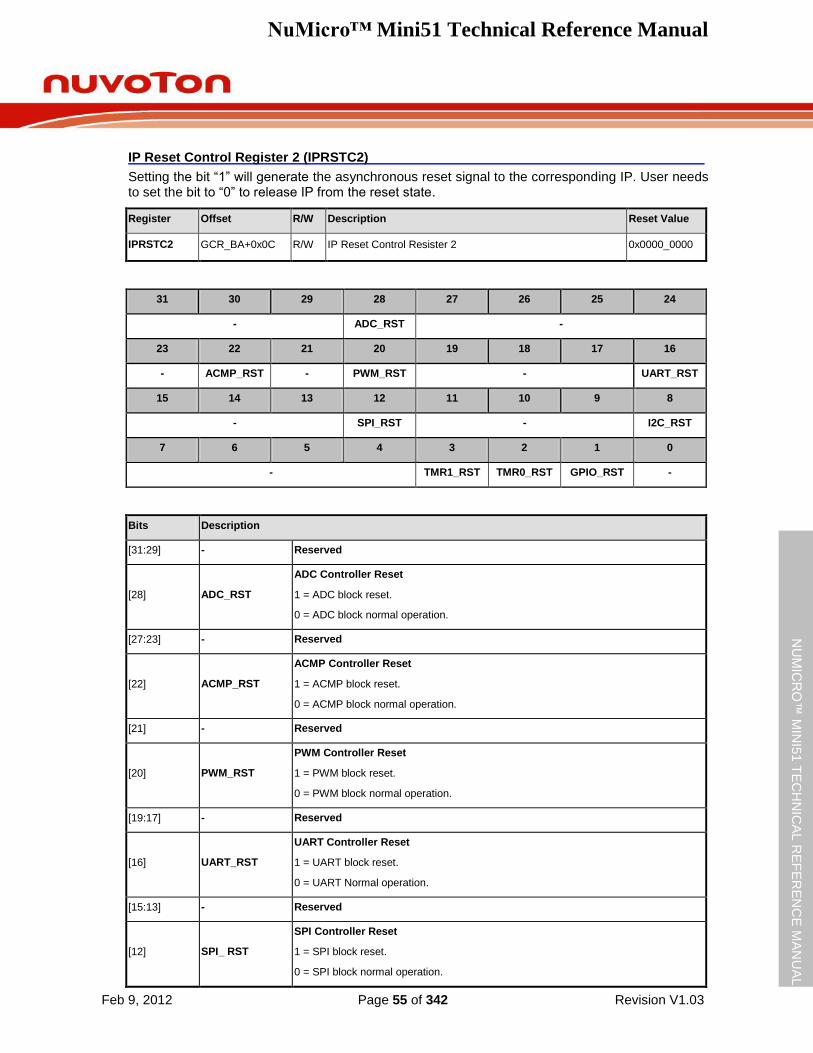
NuMicro™ Mini51 Technical Reference Manual
Feb 9, 2012 Page 55 of 342 Revision V1.03
NU
MIC
RO
™ M
INI5
1 T
EC
HN
ICA
L R
EF
ER
EN
CE
MA
NU
AL
IP Reset Control Register 2 (IPRSTC2)
Setting the bit “1” will generate the asynchronous reset signal to the corresponding IP. User needs to set the bit to “0” to release IP from the reset state.
Register Offset R/W Description Reset Value
IPRSTC2 GCR_BA+0x0C R/W IP Reset Control Resister 2 0x0000_0000
31 30 29 28 27 26 25 24
- ADC_RST -
23 22 21 20 19 18 17 16
- ACMP_RST - PWM_RST - UART_RST
15 14 13 12 11 10 9 8
- SPI_RST - I2C_RST
7 6 5 4 3 2 1 0
- TMR1_RST TMR0_RST GPIO_RST -
Bits Description
[31:29] - Reserved
[28] ADC_RST
ADC Controller Reset
1 = ADC block reset.
0 = ADC block normal operation.
[27:23] - Reserved
[22] ACMP_RST
ACMP Controller Reset
1 = ACMP block reset.
0 = ACMP block normal operation.
[21] - Reserved
[20] PWM_RST
PWM Controller Reset
1 = PWM block reset.
0 = PWM block normal operation.
[19:17] - Reserved
[16] UART_RST
UART Controller Reset
1 = UART block reset.
0 = UART Normal operation.
[15:13] - Reserved
[12] SPI_ RST
SPI Controller Reset
1 = SPI block reset.
0 = SPI block normal operation.
NuMicro™ Mini51 Technical Reference Manual
Feb 9, 2012 Page 56 of 342 Revision V1.03
NU
MIC
RO
™ M
INI5
1 T
EC
HN
ICA
L R
EF
ER
EN
CE
MA
NU
AL
Bits Description
[11:9] - Reserved
[8] I2C _RST
I2C Controller Reset
1 = I2C block reset.
0 = I2C normal operation.
[7:4] - Reserved
[3] TMR1_RST
Timer1 Controller Reset
1 = Timer1 block reset.
0 = Timer1 normal operation.
[2] TMR0_RST
Timer0 Controller Reset
1 = Timer0 block reset.
0 = Timer0 normal operation.
[1] GPIO_RST
GPIO (P0~P5) Controller Reset
1 = GPIO reset.
0 = GPIO normal operation.
[0] - Reserved
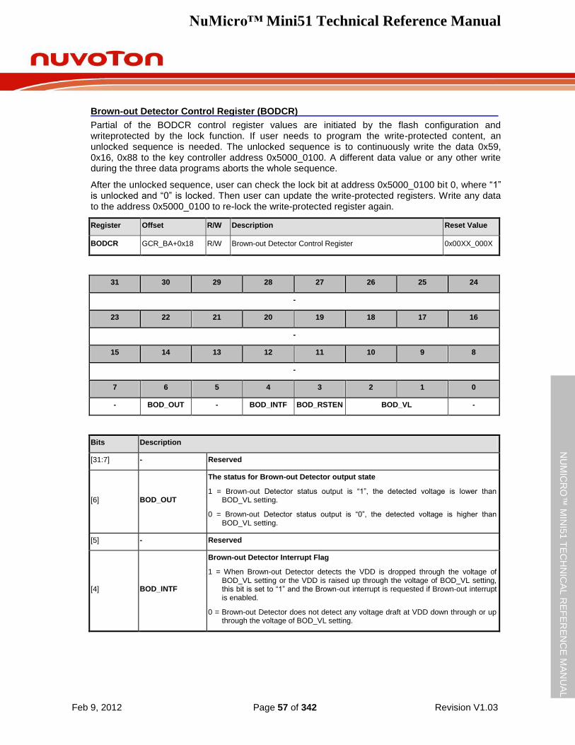
NuMicro™ Mini51 Technical Reference Manual
Feb 9, 2012 Page 57 of 342 Revision V1.03
NU
MIC
RO
™ M
INI5
1 T
EC
HN
ICA
L R
EF
ER
EN
CE
MA
NU
AL
Brown-out Detector Control Register (BODCR)
Partial of the BODCR control register values are initiated by the flash configuration and writeprotected by the lock function. If user needs to program the write-protected content, an unlocked sequence is needed. The unlocked sequence is to continuously write the data 0x59, 0x16, 0x88 to the key controller address 0x5000_0100. A different data value or any other write during the three data programs aborts the whole sequence.
After the unlocked sequence, user can check the lock bit at address 0x5000_0100 bit 0, where “1” is unlocked and “0” is locked. Then user can update the write-protected registers. Write any data to the address 0x5000_0100 to re-lock the write-protected register again.
Register Offset R/W Description Reset Value
BODCR GCR_BA+0x18 R/W Brown-out Detector Control Register 0x00XX_000X
31 30 29 28 27 26 25 24
-
23 22 21 20 19 18 17 16
-
15 14 13 12 11 10 9 8
-
7 6 5 4 3 2 1 0
- BOD_OUT - BOD_INTF BOD_RSTEN BOD_VL -
Bits Description
[31:7] - Reserved
[6] BOD_OUT
The status for Brown-out Detector output state
1 = Brown-out Detector status output is “1”, the detected voltage is lower than BOD_VL setting.
0 = Brown-out Detector status output is “0”, the detected voltage is higher than BOD_VL setting.
[5] - Reserved
[4] BOD_INTF
Brown-out Detector Interrupt Flag
1 = When Brown-out Detector detects the VDD is dropped through the voltage of BOD_VL setting or the VDD is raised up through the voltage of BOD_VL setting, this bit is set to “1” and the Brown-out interrupt is requested if Brown-out interrupt is enabled.
0 = Brown-out Detector does not detect any voltage draft at VDD down through or up through the voltage of BOD_VL setting.
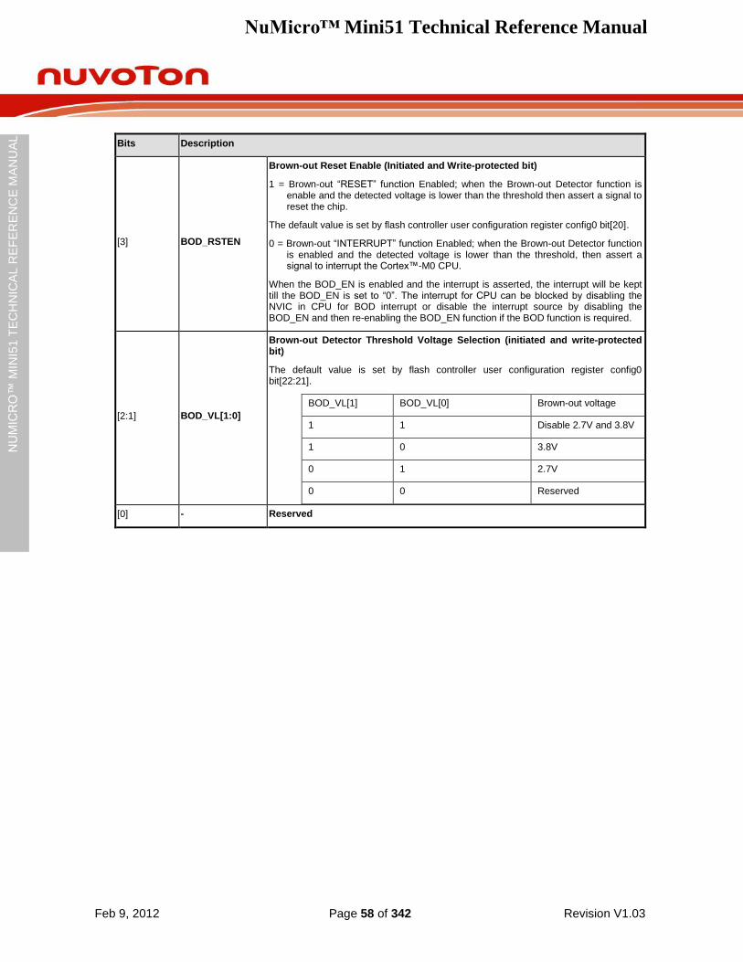
NuMicro™ Mini51 Technical Reference Manual
Feb 9, 2012 Page 58 of 342 Revision V1.03
NU
MIC
RO
™ M
INI5
1 T
EC
HN
ICA
L R
EF
ER
EN
CE
MA
NU
AL
Bits Description
[3] BOD_RSTEN
Brown-out Reset Enable (Initiated and Write-protected bit)
1 = Brown-out “RESET” function Enabled; when the Brown-out Detector function is enable and the detected voltage is lower than the threshold then assert a signal to reset the chip.
The default value is set by flash controller user configuration register config0 bit[20].
0 = Brown-out “INTERRUPT” function Enabled; when the Brown-out Detector function is enabled and the detected voltage is lower than the threshold, then assert a signal to interrupt the Cortex™-M0 CPU.
When the BOD_EN is enabled and the interrupt is asserted, the interrupt will be kept till the BOD_EN is set to “0”. The interrupt for CPU can be blocked by disabling the NVIC in CPU for BOD interrupt or disable the interrupt source by disabling the BOD_EN and then re-enabling the BOD_EN function if the BOD function is required.
[2:1] BOD_VL[1:0]
Brown-out Detector Threshold Voltage Selection (initiated and write-protected bit)
The default value is set by flash controller user configuration register config0 bit[22:21].
BOD_VL[1] BOD_VL[0] Brown-out voltage
1 1 Disable 2.7V and 3.8V
1 0 3.8V
0 1 2.7V
0 0 Reserved
[0] - Reserved

NuMicro™ Mini51 Technical Reference Manual
Feb 9, 2012 Page 59 of 342 Revision V1.03
NU
MIC
RO
™ M
INI5
1 T
EC
HN
ICA
L R
EF
ER
EN
CE
MA
NU
AL
Multiple Function Port0 Control Register (P0_MFP)
Register Offset R/W Description Reset Value
P0_MFP GCR_BA+0x30 R/W P0 Multiple Function and Input Type Control Register 0x0000_0000
31 30 29 28 27 26 25 24
-
23 22 21 20 19 18 17 16
P0_TYPE
15 14 13 12 11 10 9 8
P0_ALT
7 6 5 4 3 2 1 0
P0_MFP
Bits Description
[31:24] - Reserved
[23:16] P0_TYPE[n]
P0[7:0] input Schmitt Trigger function Enable
1 = P0[7:0] I/O input Schmitt Trigger function Enabled.
0 = P0[7:0] I/O input Schmitt Trigger function Disabled.
[15] P0_ ALT[7]
P0.7 Alternate Function Selection
The pin function of P0.7 depends on P0_MFP[7] and P0_ALT[7].
P0_ALT[7] P0_MFP[7] P0.7 function
0 0 P0.7
0 1 Reserved
1 0 SPICLK (SPI)
1 1 Reserved
[14] P0_ ALT[6]
P0.6 Alternate Function Selection
The pin function of P0.6 depends on P0_MFP[6] and P0_ALT[6].
P0_ALT[6] P0_MFP[6] P0.6 function
0 0 P0.6
0 1 Reserved
1 0 MISO (SPI)
1 1 Reserved
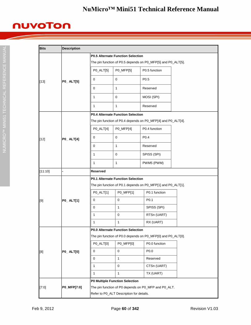
NuMicro™ Mini51 Technical Reference Manual
Feb 9, 2012 Page 60 of 342 Revision V1.03
NU
MIC
RO
™ M
INI5
1 T
EC
HN
ICA
L R
EF
ER
EN
CE
MA
NU
AL
Bits Description
[13] P0_ ALT[5]
P0.5 Alternate Function Selection
The pin function of P0.5 depends on P0_MFP[5] and P0_ALT[5].
P0_ALT[5] P0_MFP[5] P0.5 function
0 0 P0.5
0 1 Reserved
1 0 MOSI (SPI)
1 1 Reserved
[12] P0_ ALT[4]
P0.4 Alternate Function Selection
The pin function of P0.4 depends on P0_MFP[4] and P0_ALT[4].
P0_ALT[4] P0_MFP[4] P0.4 function
0 0 P0.4
0 1 Reserved
1 0 SPISS (SPI)
1 1 PWM5 (PWM)
[11:10] - Reserved
[9] P0_ ALT[1]
P0.1 Alternate Function Selection
The pin function of P0.1 depends on P0_MFP[1] and P0_ALT[1].
P0_ALT[1] P0_MFP[1] P0.1 function
0 0 P0.1
0 1 SPISS (SPI)
1 0 RTSn (UART)
1 1 RX (UART)
[8] P0_ ALT[0]
P0.0 Alternate Function Selection
The pin function of P0.0 depends on P0_MFP[0] and P0_ALT[0].
P0_ALT[0] P0_MFP[0] P0.0 function
0 0 P0.0
0 1 Reserved
1 0 CTSn (UART)
1 1 TX (UART)
[7:0] P0_MFP[7:0]
P0 Multiple Function Selection
The pin function of P0 depends on P0_MFP and P0_ALT.
Refer to P0_ALT Description for details.
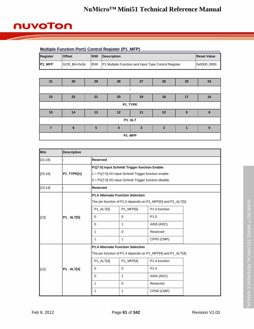
NuMicro™ Mini51 Technical Reference Manual
Feb 9, 2012 Page 61 of 342 Revision V1.03
NU
MIC
RO
™ M
INI5
1 T
EC
HN
ICA
L R
EF
ER
EN
CE
MA
NU
AL
Multiple Function Port1 Control Register (P1_MFP)
Register Offset R/W Description Reset Value
P1_MFP GCR_BA+0x34 R/W P1 Multiple Function and Input Type Control Register 0x0000_0000
31 30 29 28 27 26 25 24
-
23 22 21 20 19 18 17 16
P1_TYPE
15 14 13 12 11 10 9 8
P1_ALT
7 6 5 4 3 2 1 0
P1_MFP
Bits Description
[31:24] - Reserved
[23:16] P1_TYPE[n]
P1[7:0] input Schmitt Trigger function Enable
1 = P1[7:0] I/O input Schmitt Trigger function enable.
0 = P1[7:0] I/O input Schmitt Trigger function disable.
[15:14] - Reserved
[13] P1_ ALT[5]
P1.5 Alternate Function Selection
The pin function of P1.5 depends on P1_MFP[5] and P1_ALT[5].
P1_ALT[5] P1_MFP[5] P1.5 function
0 0 P1.5
0 1 AIN5 (ADC)
1 0 Reserved
1 1 CPP0 (CMP)
[12] P1_ ALT[4]
P1.4 Alternate Function Selection
The pin function of P1.4 depends on P1_MFP[4] and P1_ALT[4].
P1_ALT[4] P1_MFP[4] P1.4 function
0 0 P1.4
0 1 AIN4 (ADC)
1 0 Reserved
1 1 CPN0 (CMP)
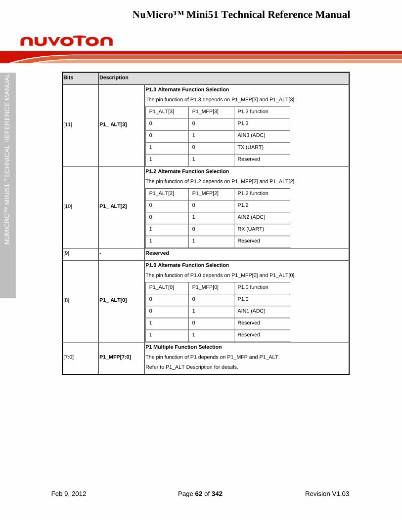
NuMicro™ Mini51 Technical Reference Manual
Feb 9, 2012 Page 62 of 342 Revision V1.03
NU
MIC
RO
™ M
INI5
1 T
EC
HN
ICA
L R
EF
ER
EN
CE
MA
NU
AL
Bits Description
[11] P1_ ALT[3]
P1.3 Alternate Function Selection
The pin function of P1.3 depends on P1_MFP[3] and P1_ALT[3].
P1_ALT[3] P1_MFP[3] P1.3 function
0 0 P1.3
0 1 AIN3 (ADC)
1 0 TX (UART)
1 1 Reserved
[10] P1_ ALT[2]
P1.2 Alternate Function Selection
The pin function of P1.2 depends on P1_MFP[2] and P1_ALT[2].
P1_ALT[2] P1_MFP[2] P1.2 function
0 0 P1.2
0 1 AIN2 (ADC)
1 0 RX (UART)
1 1 Reserved
[9] - Reserved
[8] P1_ ALT[0]
P1.0 Alternate Function Selection
The pin function of P1.0 depends on P1_MFP[0] and P1_ALT[0].
P1_ALT[0] P1_MFP[0] P1.0 function
0 0 P1.0
0 1 AIN1 (ADC)
1 0 Reserved
1 1 Reserved
[7:0] P1_MFP[7:0]
P1 Multiple Function Selection
The pin function of P1 depends on P1_MFP and P1_ALT.
Refer to P1_ALT Description for details.

NuMicro™ Mini51 Technical Reference Manual
Feb 9, 2012 Page 63 of 342 Revision V1.03
NU
MIC
RO
™ M
INI5
1 T
EC
HN
ICA
L R
EF
ER
EN
CE
MA
NU
AL
Multiple Function Port2 Control Register (P2_MFP)
Register Offset R/W Description Reset Value
P2_MFP GCR_BA+0x38 R/W P2 Multiple Function and Input Type Control Register 0x0000_0000
31 30 29 28 27 26 25 24
-
23 22 21 20 19 18 17 16
P2_TYPE
15 14 13 12 11 10 9 8
P2_ALT
7 6 5 4 3 2 1 0
P2_MFP
Bits Description
[31:24] - Reserved
[23:16] P2_TYPE[n]
P2[7:0] input Schmitt Trigger function Enable
1 = P2[7:0] I/O input Schmitt Trigger function Enabled.
0 = P2[7:0] I/O input Schmitt Trigger function Disabled.
[15] - Reserved
[14] P2_ ALT[6]
P2.6 Alternate Function Selection
The pin function of P2.6 depends on P2_MFP[6] and P2_ALT[6].
P2_ALT[6] P2_MFP[6] P2.6 function
0 0 P2.6
0 1 Reserved
1 0 PWM4 (PWM)
1 1 CPO1
[13] P2_ ALT[5]
P2.5 Alternate Function Selection
The pin function of P2.5 depends on P2_MFP[5] and P2_ALT[5].
P2_ALT[5] P2_MFP[5] P2.5 function
0 0 P2.5
0 1 Reserved
1 0 PWM3 (PWM)
1 1 Reserved
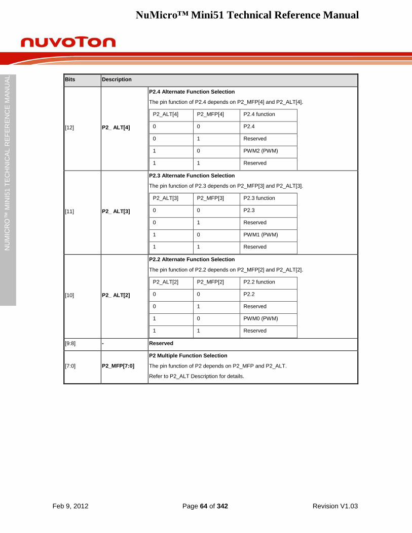
NuMicro™ Mini51 Technical Reference Manual
Feb 9, 2012 Page 64 of 342 Revision V1.03
NU
MIC
RO
™ M
INI5
1 T
EC
HN
ICA
L R
EF
ER
EN
CE
MA
NU
AL
Bits Description
[12] P2_ ALT[4]
P2.4 Alternate Function Selection
The pin function of P2.4 depends on P2_MFP[4] and P2_ALT[4].
P2_ALT[4] P2_MFP[4] P2.4 function
0 0 P2.4
0 1 Reserved
1 0 PWM2 (PWM)
1 1 Reserved
[11] P2_ ALT[3]
P2.3 Alternate Function Selection
The pin function of P2.3 depends on P2_MFP[3] and P2_ALT[3].
P2_ALT[3] P2_MFP[3] P2.3 function
0 0 P2.3
0 1 Reserved
1 0 PWM1 (PWM)
1 1 Reserved
[10] P2_ ALT[2]
P2.2 Alternate Function Selection
The pin function of P2.2 depends on P2_MFP[2] and P2_ALT[2].
P2_ALT[2] P2_MFP[2] P2.2 function
0 0 P2.2
0 1 Reserved
1 0 PWM0 (PWM)
1 1 Reserved
[9:8] - Reserved
[7:0] P2_MFP[7:0]
P2 Multiple Function Selection
The pin function of P2 depends on P2_MFP and P2_ALT.
Refer to P2_ALT Description for details.

NuMicro™ Mini51 Technical Reference Manual
Feb 9, 2012 Page 65 of 342 Revision V1.03
NU
MIC
RO
™ M
INI5
1 T
EC
HN
ICA
L R
EF
ER
EN
CE
MA
NU
AL
Multiple Function Port3 Control Register (P3_MFP)
Register Offset R/W Description Reset Value
P3_MFP GCR_BA+0x3C R/W P3 Multiple Function and Input Type Control Register 0x0000_0000
31 30 29 28 27 26 25 24
-
23 22 21 20 19 18 17 16
P3_TYPE
15 14 13 12 11 10 9 8
P3_ALT
7 6 5 4 3 2 1 0
P3_MFP
Bits Description
[31:24] - Reserved
[23:16] P3_TYPE[n]
P3[7:0] input Schmitt Trigger function Enable
1 = P3[7:0] I/O input Schmitt Trigger function Enabled.
0 = P3[7:0] I/O input Schmitt Trigger function Disabled.
[15] - Reserved
[14] P3_ ALT[6]
P3.6 Alternate Function Selection
The pin function of P3.6 depends on P3_MFP[6] and P3_ALT[6].
P3_ALT[6] P3_MFP[6] P3.6 function
0 0 P3.6
0 1 T1EX
1 0 CKO (Clock Driver output)
1 1 CPO0 (CMP)
[13] P3_ ALT[5]
P3.5 Alternate Function Selection
The pin function of P3.5 depends on P3_MFP[5] and P3_ALT[5].
P3_ALT[5] P3_MFP[5] P3.5 function
0 0 P3.5
0 1 T1 (Timer1)
1 0 SCL (I2C)
1 1 Reserved
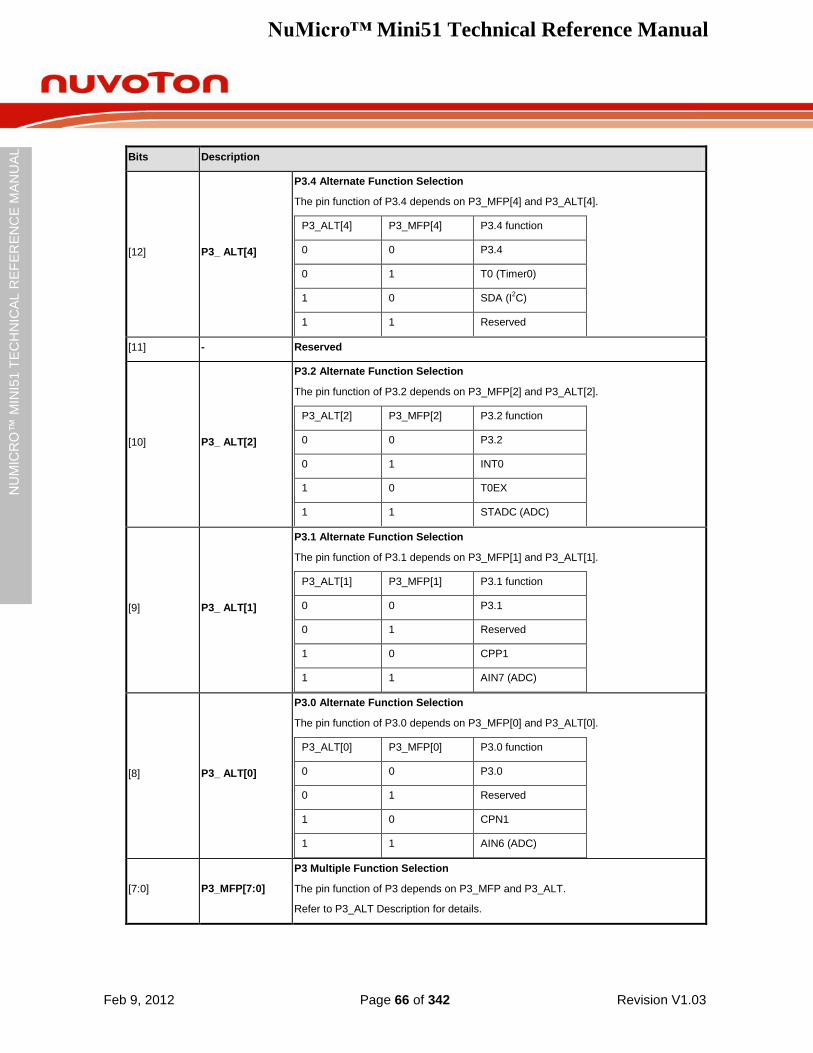
NuMicro™ Mini51 Technical Reference Manual
Feb 9, 2012 Page 66 of 342 Revision V1.03
NU
MIC
RO
™ M
INI5
1 T
EC
HN
ICA
L R
EF
ER
EN
CE
MA
NU
AL
Bits Description
[12] P3_ ALT[4]
P3.4 Alternate Function Selection
The pin function of P3.4 depends on P3_MFP[4] and P3_ALT[4].
P3_ALT[4] P3_MFP[4] P3.4 function
0 0 P3.4
0 1 T0 (Timer0)
1 0 SDA (I2C)
1 1 Reserved
[11] - Reserved
[10] P3_ ALT[2]
P3.2 Alternate Function Selection
The pin function of P3.2 depends on P3_MFP[2] and P3_ALT[2].
P3_ALT[2] P3_MFP[2] P3.2 function
0 0 P3.2
0 1 INT0
1 0 T0EX
1 1 STADC (ADC)
[9] P3_ ALT[1]
P3.1 Alternate Function Selection
The pin function of P3.1 depends on P3_MFP[1] and P3_ALT[1].
P3_ALT[1] P3_MFP[1] P3.1 function
0 0 P3.1
0 1 Reserved
1 0 CPP1
1 1 AIN7 (ADC)
[8] P3_ ALT[0]
P3.0 Alternate Function Selection
The pin function of P3.0 depends on P3_MFP[0] and P3_ALT[0].
P3_ALT[0] P3_MFP[0] P3.0 function
0 0 P3.0
0 1 Reserved
1 0 CPN1
1 1 AIN6 (ADC)
[7:0] P3_MFP[7:0]
P3 Multiple Function Selection
The pin function of P3 depends on P3_MFP and P3_ALT.
Refer to P3_ALT Description for details.
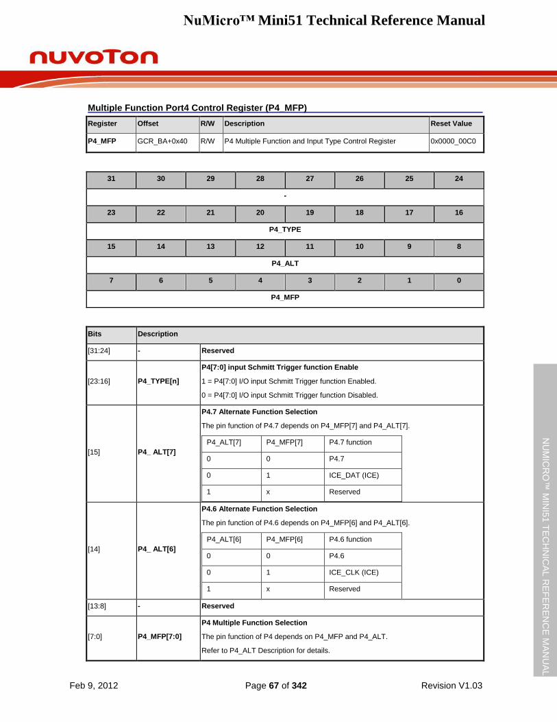
NuMicro™ Mini51 Technical Reference Manual
Feb 9, 2012 Page 67 of 342 Revision V1.03
NU
MIC
RO
™ M
INI5
1 T
EC
HN
ICA
L R
EF
ER
EN
CE
MA
NU
AL
Multiple Function Port4 Control Register (P4_MFP)
Register Offset R/W Description Reset Value
P4_MFP GCR_BA+0x40 R/W P4 Multiple Function and Input Type Control Register 0x0000_00C0
31 30 29 28 27 26 25 24
-
23 22 21 20 19 18 17 16
P4_TYPE
15 14 13 12 11 10 9 8
P4_ALT
7 6 5 4 3 2 1 0
P4_MFP
Bits Description
[31:24] - Reserved
[23:16] P4_TYPE[n]
P4[7:0] input Schmitt Trigger function Enable
1 = P4[7:0] I/O input Schmitt Trigger function Enabled.
0 = P4[7:0] I/O input Schmitt Trigger function Disabled.
[15] P4_ ALT[7]
P4.7 Alternate Function Selection
The pin function of P4.7 depends on P4_MFP[7] and P4_ALT[7].
P4_ALT[7] P4_MFP[7] P4.7 function
0 0 P4.7
0 1 ICE_DAT (ICE)
1 x Reserved
[14] P4_ ALT[6]
P4.6 Alternate Function Selection
The pin function of P4.6 depends on P4_MFP[6] and P4_ALT[6].
P4_ALT[6] P4_MFP[6] P4.6 function
0 0 P4.6
0 1 ICE_CLK (ICE)
1 x Reserved
[13:8] - Reserved
[7:0] P4_MFP[7:0]
P4 Multiple Function Selection
The pin function of P4 depends on P4_MFP and P4_ALT.
Refer to P4_ALT Description for details.
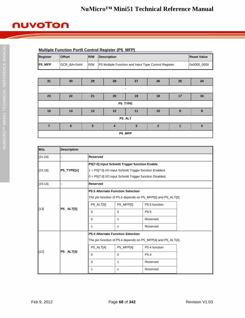
NuMicro™ Mini51 Technical Reference Manual
Feb 9, 2012 Page 68 of 342 Revision V1.03
NU
MIC
RO
™ M
INI5
1 T
EC
HN
ICA
L R
EF
ER
EN
CE
MA
NU
AL
Multiple Function Port5 Control Register (P5_MFP)
Register Offset R/W Description Reset Value
P5_MFP GCR_BA+0x44 R/W P5 Multiple Function and Input Type Control Register 0x0000_0000
31 30 29 28 27 26 25 24
-
23 22 21 20 19 18 17 16
P5_TYPE
15 14 13 12 11 10 9 8
P5_ALT
7 6 5 4 3 2 1 0
P5_MFP
Bits Description
[31:24] - Reserved
[23:16] P5_TYPE[n]
P5[7:0] input Schmitt Trigger function Enable
1 = P5[7:0] I/O input Schmitt Trigger function Enabled.
0 = P5[7:0] I/O input Schmitt Trigger function Disabled.
[15:14] - Reserved
[13] P5_ ALT[5]
P5.5 Alternate Function Selection
The pin function of P5.5 depends on P5_MFP[5] and P5_ALT[5].
P5_ALT[5] P5_MFP[5] P5.5 function
0 0 P5.5
0 1 Reserved
1 x Reserved
[12] P5_ ALT[4]
P5.4 Alternate Function Selection
The pin function of P5.4 depends on P5_MFP[4] and P5_ALT[4].
P5_ALT[4] P5_MFP[4] P5.4 function
0 0 P5.4
0 1 Reserved
1 x Reserved
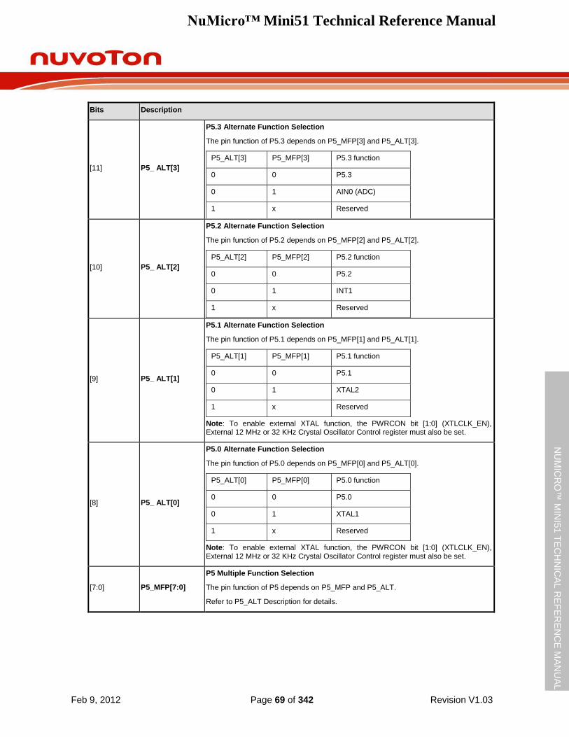
NuMicro™ Mini51 Technical Reference Manual
Feb 9, 2012 Page 69 of 342 Revision V1.03
NU
MIC
RO
™ M
INI5
1 T
EC
HN
ICA
L R
EF
ER
EN
CE
MA
NU
AL
Bits Description
[11] P5_ ALT[3]
P5.3 Alternate Function Selection
The pin function of P5.3 depends on P5_MFP[3] and P5_ALT[3].
P5_ALT[3] P5_MFP[3] P5.3 function
0 0 P5.3
0 1 AIN0 (ADC)
1 x Reserved
[10] P5_ ALT[2]
P5.2 Alternate Function Selection
The pin function of P5.2 depends on P5_MFP[2] and P5_ALT[2].
P5_ALT[2] P5_MFP[2] P5.2 function
0 0 P5.2
0 1 INT1
1 x Reserved
[9] P5_ ALT[1]
P5.1 Alternate Function Selection
The pin function of P5.1 depends on P5_MFP[1] and P5_ALT[1].
P5_ALT[1] P5_MFP[1] P5.1 function
0 0 P5.1
0 1 XTAL2
1 x Reserved
Note: To enable external XTAL function, the PWRCON bit [1:0] (XTLCLK_EN), External 12 MHz or 32 KHz Crystal Oscillator Control register must also be set.
[8] P5_ ALT[0]
P5.0 Alternate Function Selection
The pin function of P5.0 depends on P5_MFP[0] and P5_ALT[0].
P5_ALT[0] P5_MFP[0] P5.0 function
0 0 P5.0
0 1 XTAL1
1 x Reserved
Note: To enable external XTAL function, the PWRCON bit [1:0] (XTLCLK_EN), External 12 MHz or 32 KHz Crystal Oscillator Control register must also be set.
[7:0] P5_MFP[7:0]
P5 Multiple Function Selection
The pin function of P5 depends on P5_MFP and P5_ALT.
Refer to P5_ALT Description for details.
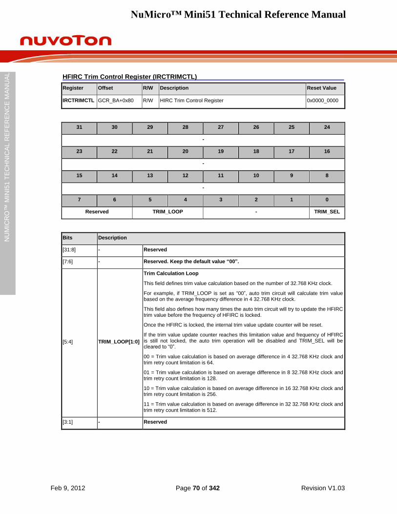
NuMicro™ Mini51 Technical Reference Manual
Feb 9, 2012 Page 70 of 342 Revision V1.03
NU
MIC
RO
™ M
INI5
1 T
EC
HN
ICA
L R
EF
ER
EN
CE
MA
NU
AL
HFIRC Trim Control Register (IRCTRIMCTL)
Register Offset R/W Description Reset Value
IRCTRIMCTL GCR_BA+0x80 R/W HIRC Trim Control Register 0x0000_0000
31 30 29 28 27 26 25 24
-
23 22 21 20 19 18 17 16
-
15 14 13 12 11 10 9 8
-
7 6 5 4 3 2 1 0
Reserved TRIM_LOOP - TRIM_SEL
Bits Description
[31:8] - Reserved
[7:6] - Reserved. Keep the default value “00”.
[5:4] TRIM_LOOP[1:0]
Trim Calculation Loop
This field defines trim value calculation based on the number of 32.768 KHz clock.
For example, if TRIM_LOOP is set as “00”, auto trim circuit will calculate trim value based on the average frequency difference in 4 32.768 KHz clock.
This field also defines how many times the auto trim circuit will try to update the HFIRC trim value before the frequency of HFIRC is locked.
Once the HFIRC is locked, the internal trim value update counter will be reset.
If the trim value update counter reaches this limitation value and frequency of HFIRC is still not locked, the auto trim operation will be disabled and TRIM_SEL will be cleared to “0”.
00 = Trim value calculation is based on average difference in 4 32.768 KHz clock and trim retry count limitation is 64.
01 = Trim value calculation is based on average difference in 8 32.768 KHz clock and trim retry count limitation is 128.
10 = Trim value calculation is based on average difference in 16 32.768 KHz clock and trim retry count limitation is 256.
11 = Trim value calculation is based on average difference in 32 32.768 KHz clock and trim retry count limitation is 512.
[3:1] - Reserved

NuMicro™ Mini51 Technical Reference Manual
Feb 9, 2012 Page 71 of 342 Revision V1.03
NU
MIC
RO
™ M
INI5
1 T
EC
HN
ICA
L R
EF
ER
EN
CE
MA
NU
AL
Bits Description
[0] TRIM_SEL
Trim Frequency Selection
This bit is to enable the HFIRC auto trim.
When setting this bit to “1”, the HFIRC auto trim function will trim HFIRC to 22 MHz automatically based on the 32.768 KHz reference clock.
During auto trim operation, if 32.768 KHz clock error is detected or trim retry limitation count reached, this field will be cleared to “0” automatically.
0 = HFIRC auto trim function Disabled.
1 = HFIRC auto trim function Enabled and HFIRC trimmed to 22 MHz.
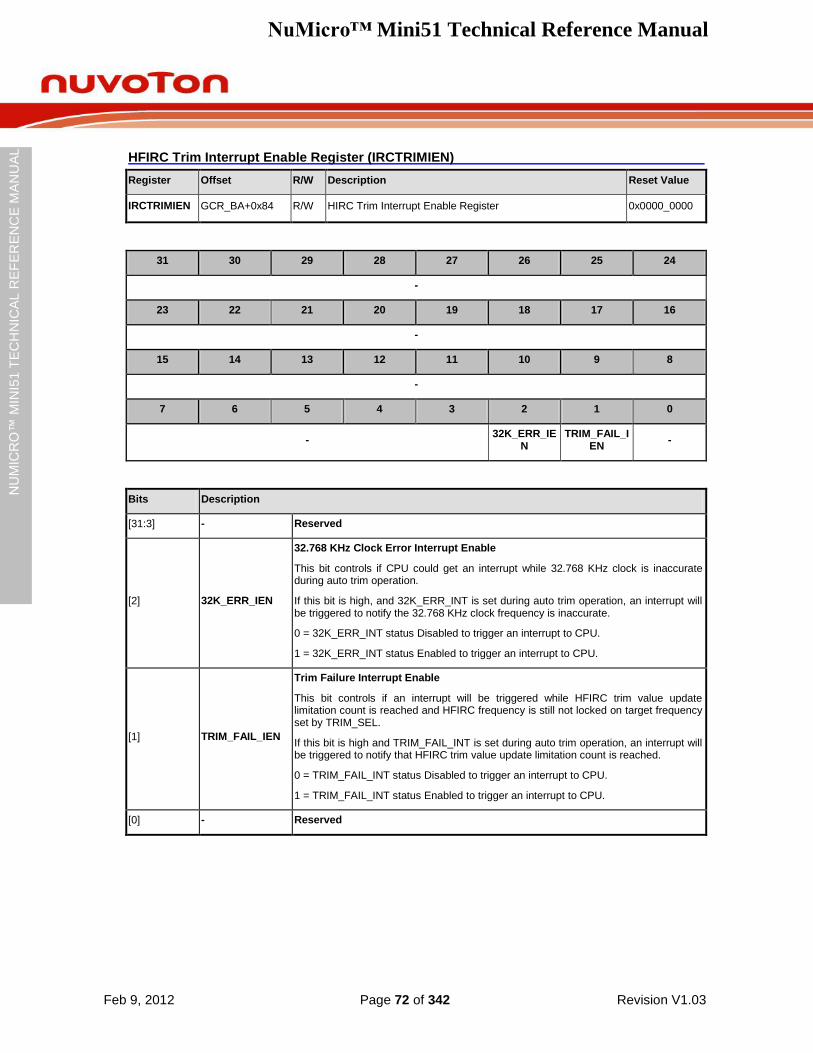
NuMicro™ Mini51 Technical Reference Manual
Feb 9, 2012 Page 72 of 342 Revision V1.03
NU
MIC
RO
™ M
INI5
1 T
EC
HN
ICA
L R
EF
ER
EN
CE
MA
NU
AL
HFIRC Trim Interrupt Enable Register (IRCTRIMIEN)
Register Offset R/W Description Reset Value
IRCTRIMIEN GCR_BA+0x84 R/W HIRC Trim Interrupt Enable Register 0x0000_0000
31 30 29 28 27 26 25 24
-
23 22 21 20 19 18 17 16
-
15 14 13 12 11 10 9 8
-
7 6 5 4 3 2 1 0
- 32K_ERR_IE
N TRIM_FAIL_I
EN -
Bits Description
[31:3] - Reserved
[2] 32K_ERR_IEN
32.768 KHz Clock Error Interrupt Enable
This bit controls if CPU could get an interrupt while 32.768 KHz clock is inaccurate during auto trim operation.
If this bit is high, and 32K_ERR_INT is set during auto trim operation, an interrupt will be triggered to notify the 32.768 KHz clock frequency is inaccurate.
0 = 32K_ERR_INT status Disabled to trigger an interrupt to CPU.
1 = 32K_ERR_INT status Enabled to trigger an interrupt to CPU.
[1] TRIM_FAIL_IEN
Trim Failure Interrupt Enable
This bit controls if an interrupt will be triggered while HFIRC trim value update limitation count is reached and HFIRC frequency is still not locked on target frequency set by TRIM_SEL.
If this bit is high and TRIM_FAIL_INT is set during auto trim operation, an interrupt will be triggered to notify that HFIRC trim value update limitation count is reached.
0 = TRIM_FAIL_INT status Disabled to trigger an interrupt to CPU.
1 = TRIM_FAIL_INT status Enabled to trigger an interrupt to CPU.
[0] - Reserved
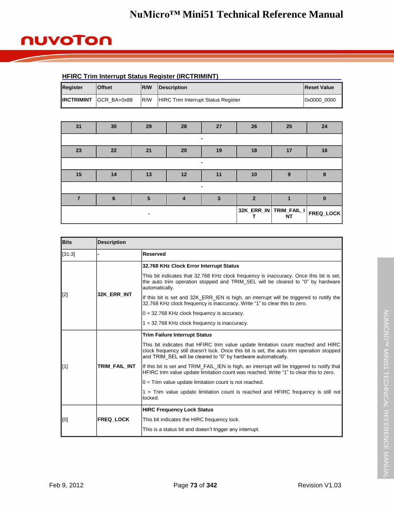
NuMicro™ Mini51 Technical Reference Manual
Feb 9, 2012 Page 73 of 342 Revision V1.03
NU
MIC
RO
™ M
INI5
1 T
EC
HN
ICA
L R
EF
ER
EN
CE
MA
NU
AL
HFIRC Trim Interrupt Status Register (IRCTRIMINT)
Register Offset R/W Description Reset Value
IRCTRIMINT GCR_BA+0x88 R/W HIRC Trim Interrupt Status Register 0x0000_0000
31 30 29 28 27 26 25 24
-
23 22 21 20 19 18 17 16
-
15 14 13 12 11 10 9 8
-
7 6 5 4 3 2 1 0
- 32K_ERR_IN
T TRIM_FAIL_I
NT FREQ_LOCK
Bits Description
[31:3] - Reserved
[2] 32K_ERR_INT
32.768 KHz Clock Error Interrupt Status
This bit indicates that 32.768 KHz clock frequency is inaccuracy. Once this bit is set, the auto trim operation stopped and TRIM_SEL will be cleared to “0” by hardware automatically.
If this bit is set and 32K_ERR_IEN is high, an interrupt will be triggered to notify the 32.768 KHz clock frequency is inaccuracy. Write “1” to clear this to zero.
0 = 32.768 KHz clock frequency is accuracy.
1 = 32.768 KHz clock frequency is inaccuracy.
[1] TRIM_FAIL_INT
Trim Failure Interrupt Status
This bit indicates that HFIRC trim value update limitation count reached and HIRC clock frequency still doesn‟t lock. Once this bit is set, the auto trim operation stopped and TRIM_SEL will be cleared to “0” by hardware automatically.
If this bit is set and TRIM_FAIL_IEN is high, an interrupt will be triggered to notify that HFIRC trim value update limitation count was reached. Write “1” to clear this to zero.
0 = Trim value update limitation count is not reached.
1 = Trim value update limitation count is reached and HFIRC frequency is still not locked.
[0] FREQ_LOCK
HIRC Frequency Lock Status
This bit indicates the HIRC frequency lock.
This is a status bit and doesn‟t trigger any interrupt.
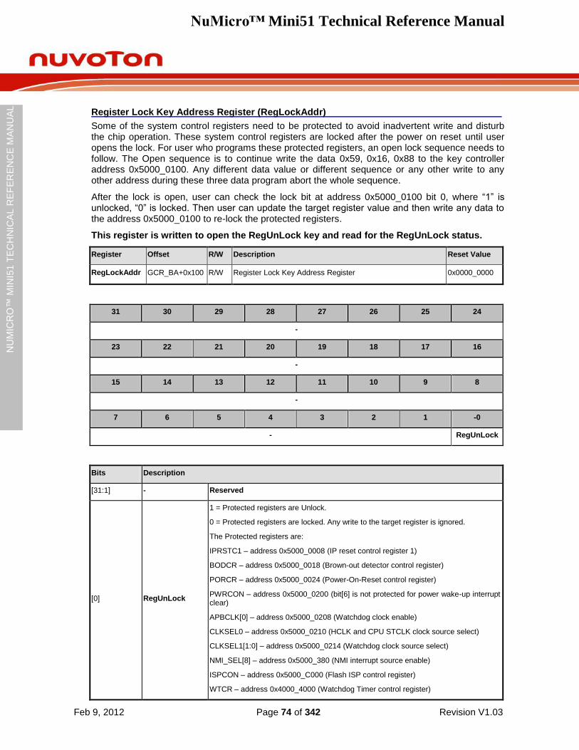
NuMicro™ Mini51 Technical Reference Manual
Feb 9, 2012 Page 74 of 342 Revision V1.03
NU
MIC
RO
™ M
INI5
1 T
EC
HN
ICA
L R
EF
ER
EN
CE
MA
NU
AL
Register Lock Key Address Register (RegLockAddr)
Some of the system control registers need to be protected to avoid inadvertent write and disturb the chip operation. These system control registers are locked after the power on reset until user opens the lock. For user who programs these protected registers, an open lock sequence needs to follow. The Open sequence is to continue write the data 0x59, 0x16, 0x88 to the key controller address 0x5000_0100. Any different data value or different sequence or any other write to any other address during these three data program abort the whole sequence.
After the lock is open, user can check the lock bit at address 0x5000_0100 bit 0, where “1” is unlocked, “0” is locked. Then user can update the target register value and then write any data to the address 0x5000_0100 to re-lock the protected registers.
This register is written to open the RegUnLock key and read for the RegUnLock status.
Register Offset R/W Description Reset Value
RegLockAddr GCR_BA+0x100 R/W Register Lock Key Address Register 0x0000_0000
31 30 29 28 27 26 25 24
-
23 22 21 20 19 18 17 16
-
15 14 13 12 11 10 9 8
-
7 6 5 4 3 2 1 -0
- RegUnLock
Bits Description
[31:1] - Reserved
[0] RegUnLock
1 = Protected registers are Unlock.
0 = Protected registers are locked. Any write to the target register is ignored.
The Protected registers are:
IPRSTC1 – address 0x5000_0008 (IP reset control register 1)
BODCR – address 0x5000_0018 (Brown-out detector control register)
PORCR – address 0x5000_0024 (Power-On-Reset control register)
PWRCON – address 0x5000_0200 (bit[6] is not protected for power wake-up interrupt clear)
APBCLK[0] – address 0x5000_0208 (Watchdog clock enable)
CLKSEL0 – address 0x5000_0210 (HCLK and CPU STCLK clock source select)
CLKSEL1[1:0] – address 0x5000_0214 (Watchdog clock source select)
NMI_SEL[8] – address 0x5000_380 (NMI interrupt source enable)
ISPCON – address 0x5000_C000 (Flash ISP control register)
WTCR – address 0x4000_4000 (Watchdog Timer control register)
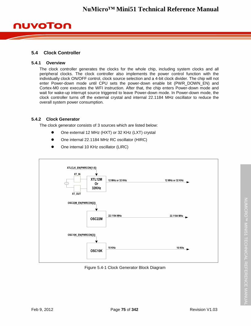
NuMicro™ Mini51 Technical Reference Manual
Feb 9, 2012 Page 75 of 342 Revision V1.03
NU
MIC
RO
™ M
INI5
1 T
EC
HN
ICA
L R
EF
ER
EN
CE
MA
NU
AL
5.4 Clock Controller
5.4.1 Overview
The clock controller generates the clocks for the whole chip, including system clocks and all peripheral clocks. The clock controller also implements the power control function with the individually clock ON/OFF control, clock source selection and a 4-bit clock divider. The chip will not enter Power-down mode until CPU sets the power-down enable bit (PWR_DOWN_EN) and Cortex-M0 core executes the WFI instruction. After that, the chip enters Power-down mode and wait for wake-up interrupt source triggered to leave Power-down mode. In Power-down mode, the clock controller turns off the external crystal and internal 22.1184 MHz oscillator to reduce the overall system power consumption.
5.4.2 Clock Generator
The clock generator consists of 3 sources which are listed below:
One external 12 MHz (HXT) or 32 KHz (LXT) crystal
One internal 22.1184 MHz RC oscillator (HIRC)
One internal 10 KHz oscillator (LIRC)
XT_OUT
XTL12M
Or
32KHz
12 MHz or 32 KHz
XTLCLK_EN(PWRCON[1:0])
XT_IN
OSC22M22.1184 MHz
OSC22M_EN(PWRCON[2])
OSC10K10 KHz
OSC10K_EN(PWRCON[3])
12 MHz or 32 KHz
22.1184 MHz
10 KHz
Figure 5.4-1 Clock Generator Block Diagram
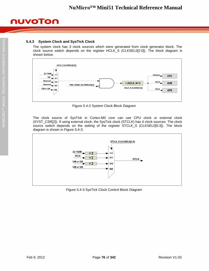
NuMicro™ Mini51 Technical Reference Manual
Feb 9, 2012 Page 76 of 342 Revision V1.03
NU
MIC
RO
™ M
INI5
1 T
EC
HN
ICA
L R
EF
ER
EN
CE
MA
NU
AL
5.4.3 System Clock and SysTick Clock
The system clock has 3 clock sources which were generated from clock generator block. The clock source switch depends on the register HCLK_S (CLKSEL0[2:0]). The block diagram is shown below.
11122.1184M
10K
12M or 32K
011
010
000
HCLK_S (CLKSEL0[2:0])
HCLK
PWD_DOWN_EN (PWRCON[7])÷ (HCLK_N+1)
HCLK_N (CLKDIV[3:0])
CPUCLK
PCLK
CPU
AHB
APB
Reserved
001Reserved
Figure 5.4-2 System Clock Block Diagram
The clock source of SysTick in Cortex-M0 core can use CPU clock or external clock (SYST_CSR[2]). If using external clock, the SysTick clock (STCLK) has 4 clock sources. The clock source switch depends on the setting of the register STCLK_S (CLKSEL0[5:3]). The block diagram is shown in Figure 5.4-3.
22.1184M
12M or 32K
STCLK_S (CLKSEL0[5:3])
STCLK
÷ 2
111
011
010
000
÷ 2
12M or 32K
HCLK÷ 2
Figure 5.4-3 SysTick Clock Control Block Diagram
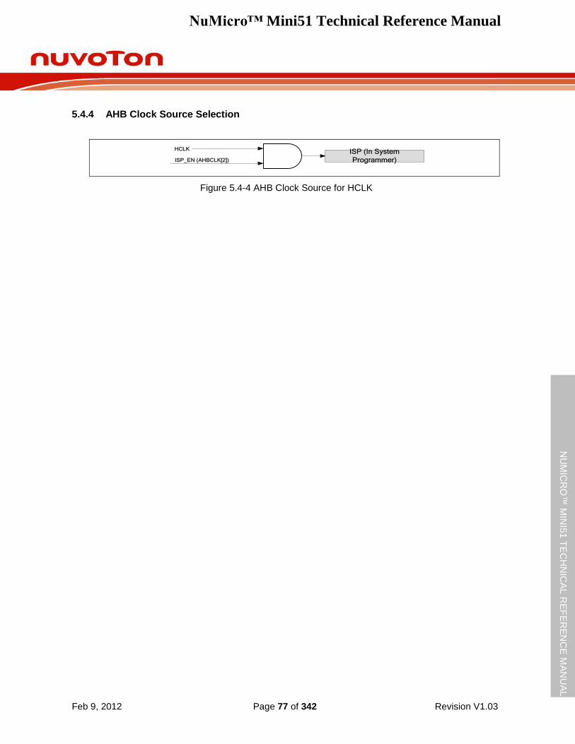
NuMicro™ Mini51 Technical Reference Manual
Feb 9, 2012 Page 77 of 342 Revision V1.03
NU
MIC
RO
™ M
INI5
1 T
EC
HN
ICA
L R
EF
ER
EN
CE
MA
NU
AL
5.4.4 AHB Clock Source Selection
ISP_EN (AHBCLK[2])
HCLK ISP (In System
Programmer)
Figure 5.4-4 AHB Clock Source for HCLK
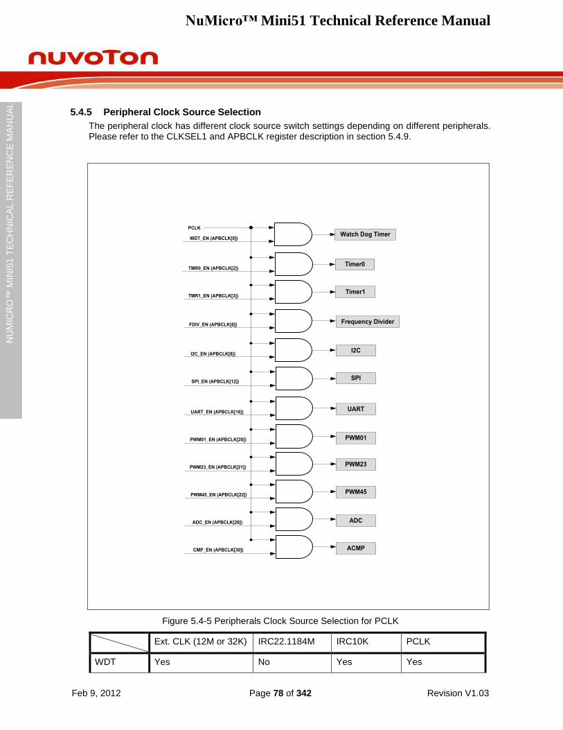
NuMicro™ Mini51 Technical Reference Manual
Feb 9, 2012 Page 78 of 342 Revision V1.03
NU
MIC
RO
™ M
INI5
1 T
EC
HN
ICA
L R
EF
ER
EN
CE
MA
NU
AL
5.4.5 Peripheral Clock Source Selection
The peripheral clock has different clock source switch settings depending on different peripherals. Please refer to the CLKSEL1 and APBCLK register description in section 5.4.9.
WDT_EN (APBCLK[0])
PCLK
Watch Dog Timer
Timer1
Timer0TMR0_EN (APBCLK[2])
TMR1_EN (APBCLK[3])
FDIV_EN (APBCLK[6])
I2C_EN (APBCLK[8])
SPI_EN (APBCLK[12])
UART_EN (APBCLK[16])
PWM01_EN (APBCLK[20])
PWM23_EN (APBCLK[21])
PWM45_EN (APBCLK[22])
CMP_EN (APBCLK[30])
ADC_EN (APBCLK[28])
Frequency Divider
I2C
SPI
UART
PWM01
PWM23
PWM45
ACMP
ADC
Figure 5.4-5 Peripherals Clock Source Selection for PCLK
Ext. CLK (12M or 32K) IRC22.1184M IRC10K PCLK
WDT Yes No Yes Yes
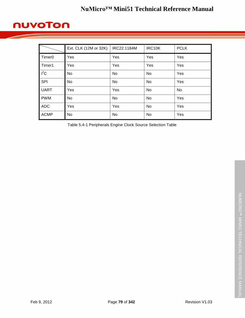
NuMicro™ Mini51 Technical Reference Manual
Feb 9, 2012 Page 79 of 342 Revision V1.03
NU
MIC
RO
™ M
INI5
1 T
EC
HN
ICA
L R
EF
ER
EN
CE
MA
NU
AL
Ext. CLK (12M or 32K) IRC22.1184M IRC10K PCLK
Timer0 Yes Yes Yes Yes
Timer1 Yes Yes Yes Yes
I2C No No No Yes
SPI No No No Yes
UART Yes Yes No No
PWM No No No Yes
ADC Yes Yes No Yes
ACMP No No No Yes
Table 5.4-1 Peripherals Engine Clock Source Selection Table
NuMicro™ Mini51 Technical Reference Manual
Feb 9, 2012 Page 80 of 342 Revision V1.03
NU
MIC
RO
™ M
INI5
1 T
EC
HN
ICA
L R
EF
ER
EN
CE
MA
NU
AL
5.4.6 Power-down Mode Clock
When entering Power-down mode, some clock sources and peripheral clocks and system clocks will be disabled. Some clock sources and peripheral clocks are still active in Power-down mode.
Clocks that still be kept active are listed below.
Clock Generator
Internal 10 KHz RC oscillator (LIRC) clock
External 32.768 KHz crystal oscillator (LXT) clock (If PD_32K = “1” and XTLCLK_EN[1:0] = “10”)
Peripherals Clock (When these IP adopt 10 KHz as clock source)
Watchdog Clock
Timer 0/1 Clock
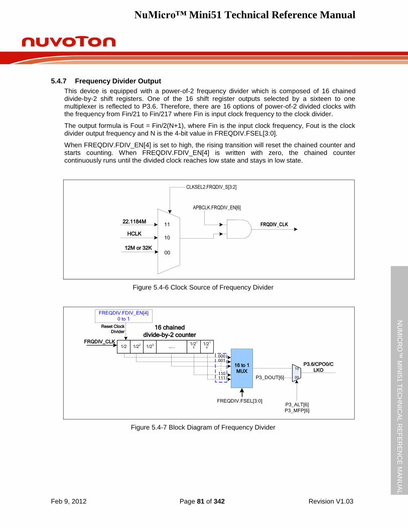
NuMicro™ Mini51 Technical Reference Manual
Feb 9, 2012 Page 81 of 342 Revision V1.03
NU
MIC
RO
™ M
INI5
1 T
EC
HN
ICA
L R
EF
ER
EN
CE
MA
NU
AL
5.4.7 Frequency Divider Output
This device is equipped with a power-of-2 frequency divider which is composed of 16 chained divide-by-2 shift registers. One of the 16 shift register outputs selected by a sixteen to one multiplexer is reflected to P3.6. Therefore, there are 16 options of power-of-2 divided clocks with the frequency from Fin/21 to Fin/217 where Fin is input clock frequency to the clock divider.
The output formula is Fout = Fin/2(N+1), where Fin is the input clock frequency, Fout is the clock divider output frequency and N is the 4-bit value in FREQDIV.FSEL[3:0].
When FREQDIV.FDIV_EN[4] is set to high, the rising transition will reset the chained counter and starts counting. When FREQDIV.FDIV_EN[4] is written with zero, the chained counter continuously runs until the divided clock reaches low state and stays in low state.
11
10
00
HCLK
12M or 32K
22.1184M
CLKSEL2.FRQDIV_S[3:2]
APBCLK.FRQDIV_EN[6]
FRQDIV_CLK
Figure 5.4-6 Clock Source of Frequency Divider
16 chained
divide-by-2 counter
1/2 …...1/22
1/23 1/2
1
51/2
1
6
000001
110111
FREQDIV.FSEL[3:0]
:
:16 to 1
MUX
FREQDIV.FDIV_EN[4]
0 to 1
Reset Clock
Divider
10
00
P3_ALT[6]
P3_MFP[6]
P3.6/CPO0/C
LKO
P3_DOUT[6]
FRQDIV_CLK
Figure 5.4-7 Block Diagram of Frequency Divider
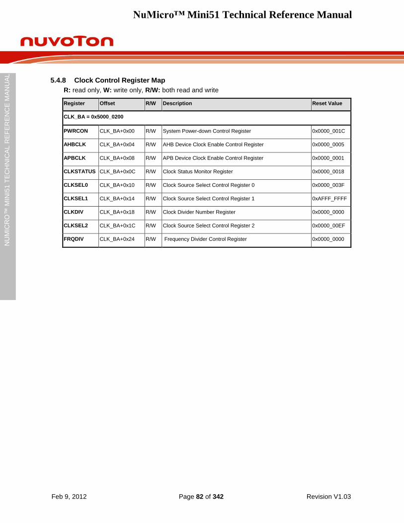
NuMicro™ Mini51 Technical Reference Manual
Feb 9, 2012 Page 82 of 342 Revision V1.03
NU
MIC
RO
™ M
INI5
1 T
EC
HN
ICA
L R
EF
ER
EN
CE
MA
NU
AL
5.4.8 Clock Control Register Map
R: read only, W: write only, R/W: both read and write
Register Offset R/W Description Reset Value
CLK_BA = 0x5000_0200
PWRCON CLK_BA+0x00 R/W System Power-down Control Register 0x0000_001C
AHBCLK CLK_BA+0x04 R/W AHB Device Clock Enable Control Register 0x0000_0005
APBCLK CLK_BA+0x08 R/W APB Device Clock Enable Control Register 0x0000_0001
CLKSTATUS CLK_BA+0x0C R/W Clock Status Monitor Register 0x0000_0018
CLKSEL0 CLK_BA+0x10 R/W Clock Source Select Control Register 0 0x0000_003F
CLKSEL1 CLK_BA+0x14 R/W Clock Source Select Control Register 1 0xAFFF_FFFF
CLKDIV CLK_BA+0x18 R/W Clock Divider Number Register 0x0000_0000
CLKSEL2 CLK_BA+0x1C R/W Clock Source Select Control Register 2 0x0000_00EF
FRQDIV CLK_BA+0x24 R/W Frequency Divider Control Register 0x0000_0000
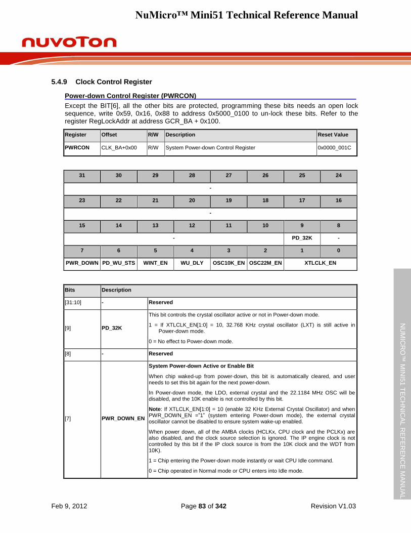
NuMicro™ Mini51 Technical Reference Manual
Feb 9, 2012 Page 83 of 342 Revision V1.03
NU
MIC
RO
™ M
INI5
1 T
EC
HN
ICA
L R
EF
ER
EN
CE
MA
NU
AL
5.4.9 Clock Control Register
Power-down Control Register (PWRCON)
Except the BIT[6], all the other bits are protected, programming these bits needs an open lock sequence, write 0x59, 0x16, 0x88 to address 0x5000_0100 to un-lock these bits. Refer to the register RegLockAddr at address GCR_BA + 0x100.
Register Offset R/W Description Reset Value
PWRCON CLK_BA+0x00 R/W System Power-down Control Register 0x0000_001C
31 30 29 28 27 26 25 24
-
23 22 21 20 19 18 17 16
-
15 14 13 12 11 10 9 8
- PD_32K -
7 6 5 4 3 2 1 0
PWR_DOWN PD_WU_STS WINT_EN WU_DLY OSC10K_EN OSC22M_EN XTLCLK_EN
Bits Description
[31:10] - Reserved
[9] PD_32K
This bit controls the crystal oscillator active or not in Power-down mode.
1 = If XTLCLK_EN[1:0] = 10, 32.768 KHz crystal oscillator (LXT) is still active in Power-down mode.
0 = No effect to Power-down mode.
[8] - Reserved
[7] PWR_DOWN_EN
System Power-down Active or Enable Bit
When chip waked-up from power-down, this bit is automatically cleared, and user needs to set this bit again for the next power-down.
In Power-down mode, the LDO, external crystal and the 22.1184 MHz OSC will be disabled, and the 10K enable is not controlled by this bit.
Note: If XTLCLK_EN[1:0] = 10 (enable 32 KHz External Crystal Oscillator) and when PWR_DOWN_EN =”1” (system entering Power-down mode), the external crystal oscillator cannot be disabled to ensure system wake-up enabled.
When power down, all of the AMBA clocks (HCLKx, CPU clock and the PCLKx) are also disabled, and the clock source selection is ignored. The IP engine clock is not controlled by this bit if the IP clock source is from the 10K clock and the WDT from 10K).
1 = Chip entering the Power-down mode instantly or wait CPU Idle command.
0 = Chip operated in Normal mode or CPU enters into Idle mode.
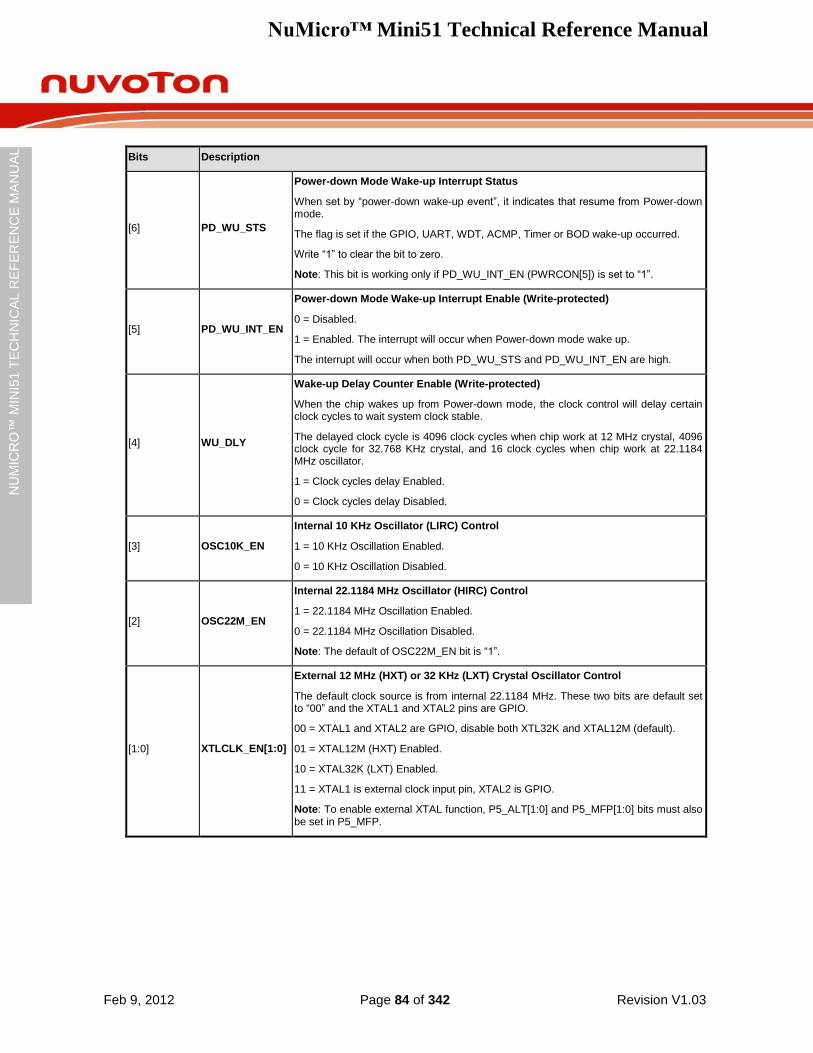
NuMicro™ Mini51 Technical Reference Manual
Feb 9, 2012 Page 84 of 342 Revision V1.03
NU
MIC
RO
™ M
INI5
1 T
EC
HN
ICA
L R
EF
ER
EN
CE
MA
NU
AL
Bits Description
[6] PD_WU_STS
Power-down Mode Wake-up Interrupt Status
When set by “power-down wake-up event”, it indicates that resume from Power-down mode.
The flag is set if the GPIO, UART, WDT, ACMP, Timer or BOD wake-up occurred.
Write “1” to clear the bit to zero.
Note: This bit is working only if PD_WU_INT_EN (PWRCON[5]) is set to “1”.
[5] PD_WU_INT_EN
Power-down Mode Wake-up Interrupt Enable (Write-protected)
0 = Disabled.
1 = Enabled. The interrupt will occur when Power-down mode wake up.
The interrupt will occur when both PD_WU_STS and PD_WU_INT_EN are high.
[4] WU_DLY
Wake-up Delay Counter Enable (Write-protected)
When the chip wakes up from Power-down mode, the clock control will delay certain clock cycles to wait system clock stable.
The delayed clock cycle is 4096 clock cycles when chip work at 12 MHz crystal, 4096 clock cycle for 32.768 KHz crystal, and 16 clock cycles when chip work at 22.1184 MHz oscillator.
1 = Clock cycles delay Enabled.
0 = Clock cycles delay Disabled.
[3] OSC10K_EN
Internal 10 KHz Oscillator (LIRC) Control
1 = 10 KHz Oscillation Enabled.
0 = 10 KHz Oscillation Disabled.
[2] OSC22M_EN
Internal 22.1184 MHz Oscillator (HIRC) Control
1 = 22.1184 MHz Oscillation Enabled.
0 = 22.1184 MHz Oscillation Disabled.
Note: The default of OSC22M_EN bit is “1”.
[1:0] XTLCLK_EN[1:0]
External 12 MHz (HXT) or 32 KHz (LXT) Crystal Oscillator Control
The default clock source is from internal 22.1184 MHz. These two bits are default set to “00” and the XTAL1 and XTAL2 pins are GPIO.
00 = XTAL1 and XTAL2 are GPIO, disable both XTL32K and XTAL12M (default).
01 = XTAL12M (HXT) Enabled.
10 = XTAL32K (LXT) Enabled.
11 = XTAL1 is external clock input pin, XTAL2 is GPIO.
Note: To enable external XTAL function, P5_ALT[1:0] and P5_MFP[1:0] bits must also be set in P5_MFP.
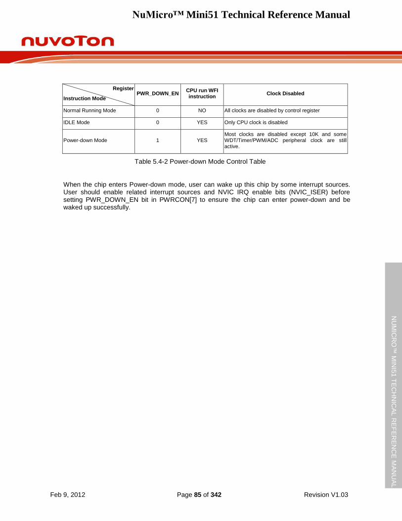
NuMicro™ Mini51 Technical Reference Manual
Feb 9, 2012 Page 85 of 342 Revision V1.03
NU
MIC
RO
™ M
INI5
1 T
EC
HN
ICA
L R
EF
ER
EN
CE
MA
NU
AL
Register
Instruction Mode PWR_DOWN_EN
CPU run WFI instruction
Clock Disabled
Normal Running Mode 0 NO All clocks are disabled by control register
IDLE Mode 0 YES Only CPU clock is disabled
Power-down Mode 1 YES Most clocks are disabled except 10K and some WDT/Timer/PWM/ADC peripheral clock are still active.
Table 5.4-2 Power-down Mode Control Table
When the chip enters Power-down mode, user can wake up this chip by some interrupt sources. User should enable related interrupt sources and NVIC IRQ enable bits (NVIC_ISER) before setting PWR_DOWN_EN bit in PWRCON[7] to ensure the chip can enter power-down and be waked up successfully.
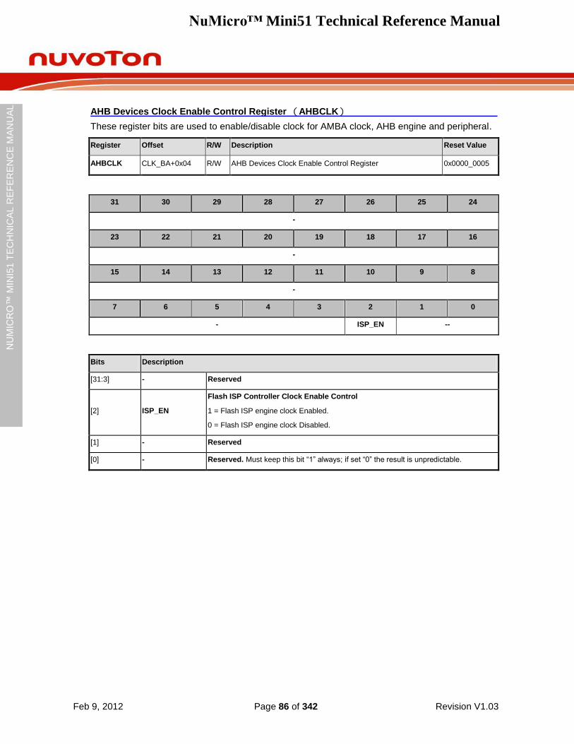
NuMicro™ Mini51 Technical Reference Manual
Feb 9, 2012 Page 86 of 342 Revision V1.03
NU
MIC
RO
™ M
INI5
1 T
EC
HN
ICA
L R
EF
ER
EN
CE
MA
NU
AL
AHB Devices Clock Enable Control Register (AHBCLK)
These register bits are used to enable/disable clock for AMBA clock, AHB engine and peripheral.
Register Offset R/W Description Reset Value
AHBCLK CLK_BA+0x04 R/W AHB Devices Clock Enable Control Register 0x0000_0005
31 30 29 28 27 26 25 24
-
23 22 21 20 19 18 17 16
-
15 14 13 12 11 10 9 8
-
7 6 5 4 3 2 1 0
- ISP_EN --
Bits Description
[31:3] - Reserved
[2] ISP_EN
Flash ISP Controller Clock Enable Control
1 = Flash ISP engine clock Enabled.
0 = Flash ISP engine clock Disabled.
[1] - Reserved
[0] - Reserved. Must keep this bit “1” always; if set “0” the result is unpredictable.
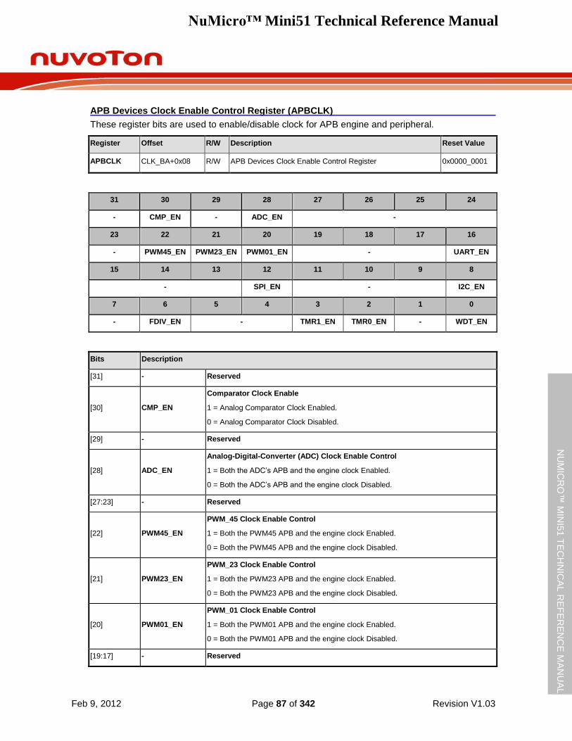
NuMicro™ Mini51 Technical Reference Manual
Feb 9, 2012 Page 87 of 342 Revision V1.03
NU
MIC
RO
™ M
INI5
1 T
EC
HN
ICA
L R
EF
ER
EN
CE
MA
NU
AL
APB Devices Clock Enable Control Register (APBCLK)
These register bits are used to enable/disable clock for APB engine and peripheral.
Register Offset R/W Description Reset Value
APBCLK CLK_BA+0x08 R/W APB Devices Clock Enable Control Register 0x0000_0001
31 30 29 28 27 26 25 24
- CMP_EN - ADC_EN -
23 22 21 20 19 18 17 16
- PWM45_EN PWM23_EN PWM01_EN - UART_EN
15 14 13 12 11 10 9 8
- SPI_EN - I2C_EN
7 6 5 4 3 2 1 0
- FDIV_EN - TMR1_EN TMR0_EN - WDT_EN
Bits Description
[31] - Reserved
[30] CMP_EN
Comparator Clock Enable
1 = Analog Comparator Clock Enabled.
0 = Analog Comparator Clock Disabled.
[29] - Reserved
[28] ADC_EN
Analog-Digital-Converter (ADC) Clock Enable Control
1 = Both the ADC‟s APB and the engine clock Enabled.
0 = Both the ADC‟s APB and the engine clock Disabled.
[27:23] - Reserved
[22] PWM45_EN
PWM_45 Clock Enable Control
1 = Both the PWM45 APB and the engine clock Enabled.
0 = Both the PWM45 APB and the engine clock Disabled.
[21] PWM23_EN
PWM_23 Clock Enable Control
1 = Both the PWM23 APB and the engine clock Enabled.
0 = Both the PWM23 APB and the engine clock Disabled.
[20] PWM01_EN
PWM_01 Clock Enable Control
1 = Both the PWM01 APB and the engine clock Enabled.
0 = Both the PWM01 APB and the engine clock Disabled.
[19:17] - Reserved
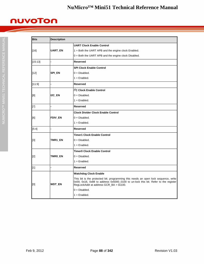
NuMicro™ Mini51 Technical Reference Manual
Feb 9, 2012 Page 88 of 342 Revision V1.03
NU
MIC
RO
™ M
INI5
1 T
EC
HN
ICA
L R
EF
ER
EN
CE
MA
NU
AL
Bits Description
[16] UART_EN
UART Clock Enable Control
1 = Both the UART APB and the engine clock Enabled.
0 = Both the UART APB and the engine clock Disabled.
[15:13] - Reserved
[12] SPI_EN
SPI Clock Enable Control
0 = Disabled.
1 = Enabled.
[11:9] - Reserved
[8] I2C_EN
I2C Clock Enable Control
0 = Disabled.
1 = Enabled.
[7] - Reserved
[6] FDIV_EN
Clock Divider Clock Enable Control
0 = Disabled.
1 = Enabled.
[5:4] - Reserved
[3] TMR1_EN
Timer1 Clock Enable Control
0 = Disabled.
1 = Enabled.
[2] TMR0_EN
Timer0 Clock Enable Control
0 = Disabled.
1 = Enabled.
[1] - Reserved
[0] WDT_EN
Watchdog Clock Enable
This bit is the protected bit; programming this needs an open lock sequence, write 0x59, 0x16, 0x88 to address 0x5000_0100 to un-lock this bit. Refer to the register RegLockAddr at address GCR_BA + 0x100.
0 = Disabled.
1 = Enabled.
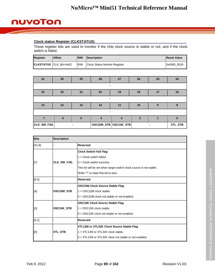
NuMicro™ Mini51 Technical Reference Manual
Feb 9, 2012 Page 89 of 342 Revision V1.03
NU
MIC
RO
™ M
INI5
1 T
EC
HN
ICA
L R
EF
ER
EN
CE
MA
NU
AL
Clock status Register (CLKSTATUS)
These register bits are used to monitor if the chip clock source is stable or not, and if the clock switch is failed.
Register Offset R/W Description Reset Value
CLKSTATUS CLK_BA+0x0C R/W Clock Status Monitor Register 0x0000_0018
31 30 29 28 27 26 25 24
-
23 22 21 20 19 18 17 16
-
15 14 13 12 11 10 9 8
-
7 6 5 4 3 2 1 0
CLK_SW_FAIL - OSC22M_STB OSC10K_STB - XTL_STB
Bits Description
[31:8] - Reserved
[7] CLK_SW_FAIL
Clock Switch Fail Flag
1 = Clock switch failed.
0 = Clock switch success.
This bit will be set when target switch clock source is not stable.
Write “1” to clear this bit to zero.
[6:5] - Reserved
[4] OSC22M_STB
OSC22M Clock Source Stable Flag
1 = OSC22M clock stable.
0 = OSC22M clock not stable or not enabled.
[3] OSC10K_STB
OSC10K Clock Source Stable Flag
1 = OSC10K clock stable.
0 = OSC10K clock not stable or not enabled.
[2:1] - Reserved
[0] XTL_STB
XTL12M or XTL32K Clock Source Stable Flag
1 = XTL12M or XTL32K clock stable.
0 = XTL12M or XTL32K clock not stable or not enabled.
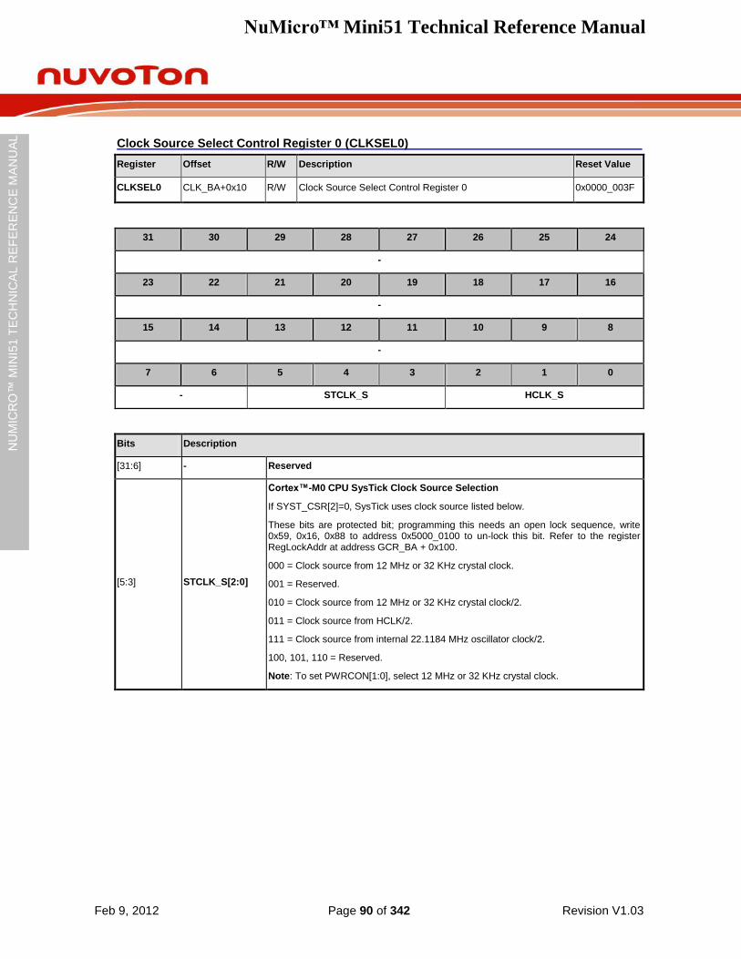
NuMicro™ Mini51 Technical Reference Manual
Feb 9, 2012 Page 90 of 342 Revision V1.03
NU
MIC
RO
™ M
INI5
1 T
EC
HN
ICA
L R
EF
ER
EN
CE
MA
NU
AL
Clock Source Select Control Register 0 (CLKSEL0)
Register Offset R/W Description Reset Value
CLKSEL0 CLK_BA+0x10 R/W Clock Source Select Control Register 0 0x0000_003F
31 30 29 28 27 26 25 24
-
23 22 21 20 19 18 17 16
-
15 14 13 12 11 10 9 8
-
7 6 5 4 3 2 1 0
- STCLK_S HCLK_S
Bits Description
[31:6] - Reserved
[5:3] STCLK_S[2:0]
Cortex™-M0 CPU SysTick Clock Source Selection
If SYST_CSR[2]=0, SysTick uses clock source listed below.
These bits are protected bit; programming this needs an open lock sequence, write 0x59, 0x16, 0x88 to address 0x5000_0100 to un-lock this bit. Refer to the register RegLockAddr at address GCR_BA + 0x100.
000 = Clock source from 12 MHz or 32 KHz crystal clock.
001 = Reserved.
010 = Clock source from 12 MHz or 32 KHz crystal clock/2.
011 = Clock source from HCLK/2.
111 = Clock source from internal 22.1184 MHz oscillator clock/2.
100, 101, 110 = Reserved.
Note: To set PWRCON[1:0], select 12 MHz or 32 KHz crystal clock.
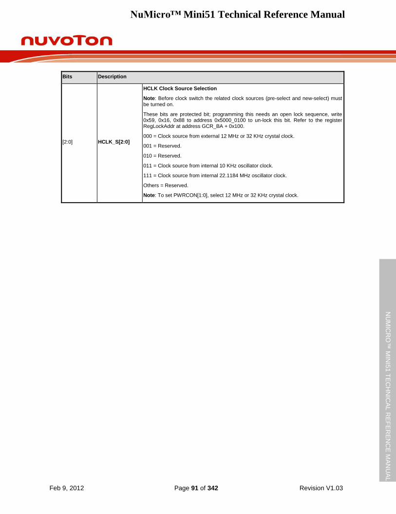
NuMicro™ Mini51 Technical Reference Manual
Feb 9, 2012 Page 91 of 342 Revision V1.03
NU
MIC
RO
™ M
INI5
1 T
EC
HN
ICA
L R
EF
ER
EN
CE
MA
NU
AL
Bits Description
[2:0] HCLK_S[2:0]
HCLK Clock Source Selection
Note: Before clock switch the related clock sources (pre-select and new-select) must be turned on.
These bits are protected bit; programming this needs an open lock sequence, write 0x59, 0x16, 0x88 to address 0x5000_0100 to un-lock this bit. Refer to the register RegLockAddr at address GCR_BA + 0x100.
000 = Clock source from external 12 MHz or 32 KHz crystal clock.
001 = Reserved.
010 = Reserved.
011 = Clock source from internal 10 KHz oscillator clock.
111 = Clock source from internal 22.1184 MHz oscillator clock.
Others = Reserved.
Note: To set PWRCON[1:0], select 12 MHz or 32 KHz crystal clock.
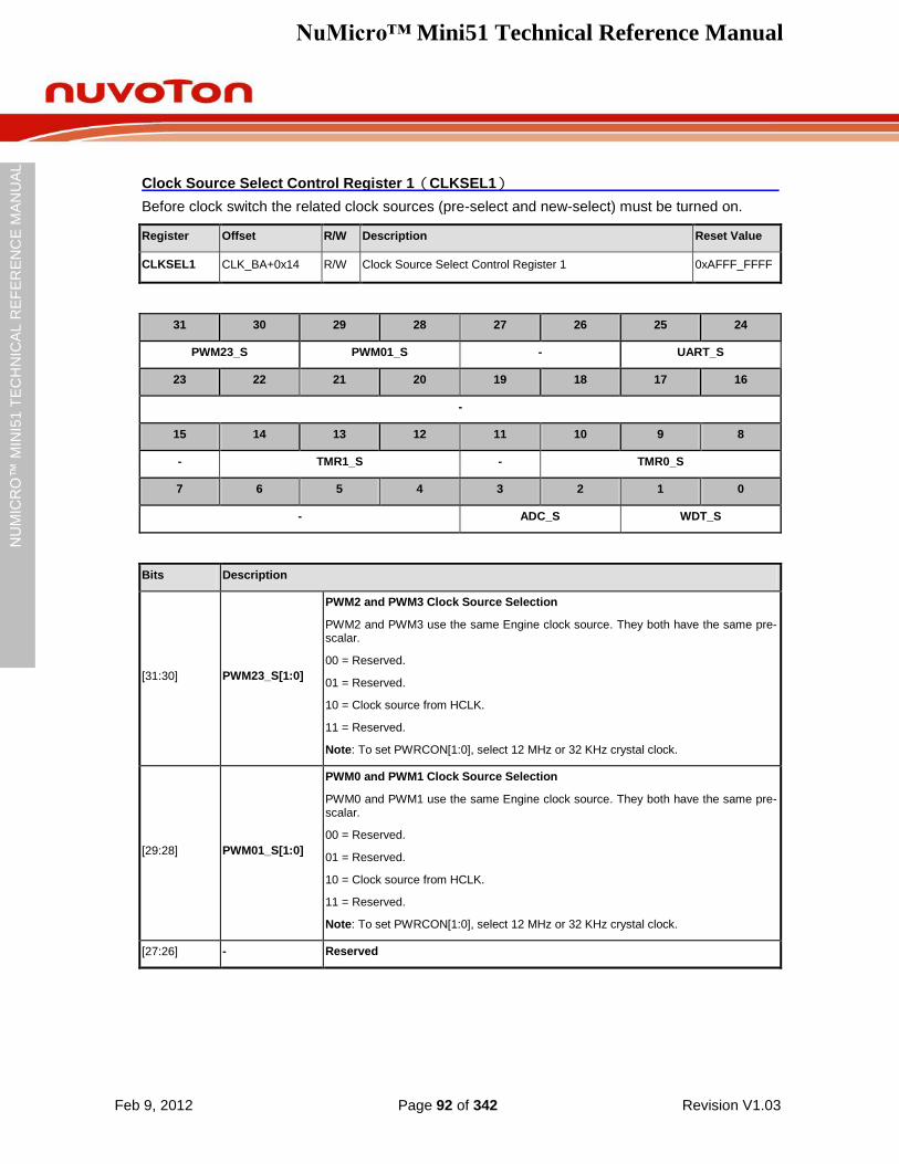
NuMicro™ Mini51 Technical Reference Manual
Feb 9, 2012 Page 92 of 342 Revision V1.03
NU
MIC
RO
™ M
INI5
1 T
EC
HN
ICA
L R
EF
ER
EN
CE
MA
NU
AL
Clock Source Select Control Register 1(CLKSEL1)
Before clock switch the related clock sources (pre-select and new-select) must be turned on.
Register Offset R/W Description Reset Value
CLKSEL1 CLK_BA+0x14 R/W Clock Source Select Control Register 1 0xAFFF_FFFF
31 30 29 28 27 26 25 24
PWM23_S PWM01_S - UART_S
23 22 21 20 19 18 17 16
-
15 14 13 12 11 10 9 8
- TMR1_S - TMR0_S
7 6 5 4 3 2 1 0
- ADC_S WDT_S
Bits Description
[31:30] PWM23_S[1:0]
PWM2 and PWM3 Clock Source Selection
PWM2 and PWM3 use the same Engine clock source. They both have the same pre-scalar.
00 = Reserved.
01 = Reserved.
10 = Clock source from HCLK.
11 = Reserved.
Note: To set PWRCON[1:0], select 12 MHz or 32 KHz crystal clock.
[29:28] PWM01_S[1:0]
PWM0 and PWM1 Clock Source Selection
PWM0 and PWM1 use the same Engine clock source. They both have the same pre-scalar.
00 = Reserved.
01 = Reserved.
10 = Clock source from HCLK.
11 = Reserved.
Note: To set PWRCON[1:0], select 12 MHz or 32 KHz crystal clock.
[27:26] - Reserved
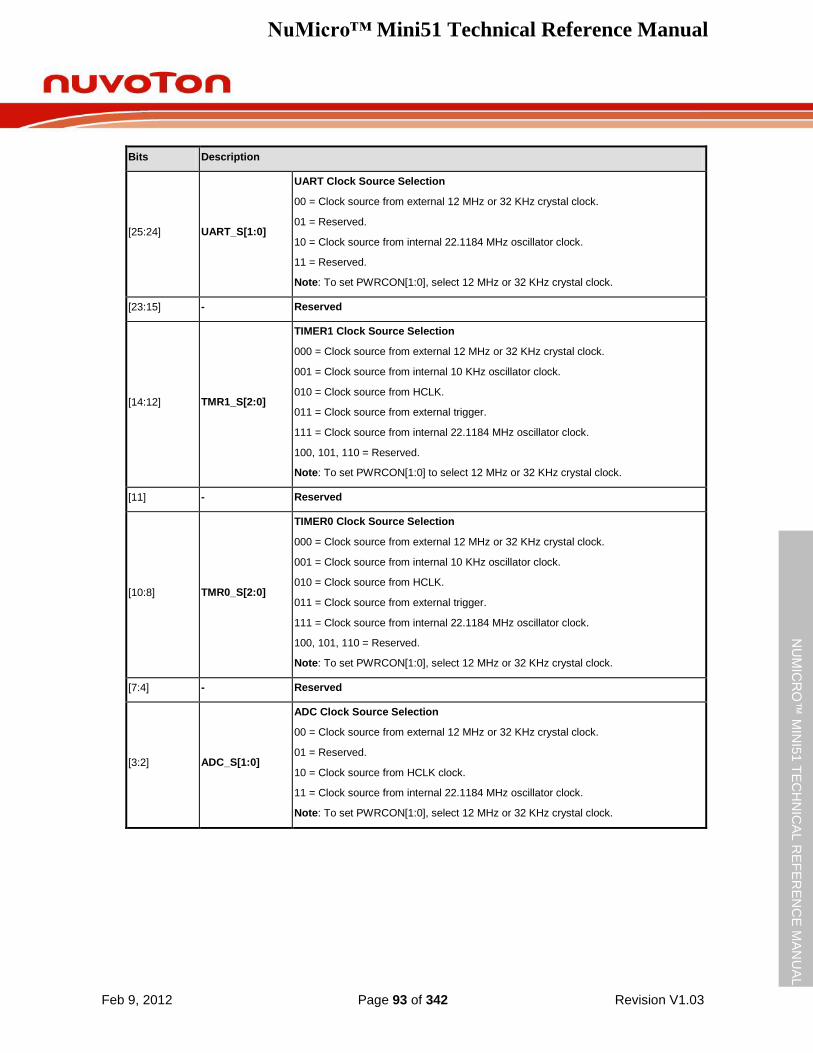
NuMicro™ Mini51 Technical Reference Manual
Feb 9, 2012 Page 93 of 342 Revision V1.03
NU
MIC
RO
™ M
INI5
1 T
EC
HN
ICA
L R
EF
ER
EN
CE
MA
NU
AL
Bits Description
[25:24] UART_S[1:0]
UART Clock Source Selection
00 = Clock source from external 12 MHz or 32 KHz crystal clock.
01 = Reserved.
10 = Clock source from internal 22.1184 MHz oscillator clock.
11 = Reserved.
Note: To set PWRCON[1:0], select 12 MHz or 32 KHz crystal clock.
[23:15] - Reserved
[14:12] TMR1_S[2:0]
TIMER1 Clock Source Selection
000 = Clock source from external 12 MHz or 32 KHz crystal clock.
001 = Clock source from internal 10 KHz oscillator clock.
010 = Clock source from HCLK.
011 = Clock source from external trigger.
111 = Clock source from internal 22.1184 MHz oscillator clock.
100, 101, 110 = Reserved.
Note: To set PWRCON[1:0] to select 12 MHz or 32 KHz crystal clock.
[11] - Reserved
[10:8] TMR0_S[2:0]
TIMER0 Clock Source Selection
000 = Clock source from external 12 MHz or 32 KHz crystal clock.
001 = Clock source from internal 10 KHz oscillator clock.
010 = Clock source from HCLK.
011 = Clock source from external trigger.
111 = Clock source from internal 22.1184 MHz oscillator clock.
100, 101, 110 = Reserved.
Note: To set PWRCON[1:0], select 12 MHz or 32 KHz crystal clock.
[7:4] - Reserved
[3:2] ADC_S[1:0]
ADC Clock Source Selection
00 = Clock source from external 12 MHz or 32 KHz crystal clock.
01 = Reserved.
10 = Clock source from HCLK clock.
11 = Clock source from internal 22.1184 MHz oscillator clock.
Note: To set PWRCON[1:0], select 12 MHz or 32 KHz crystal clock.
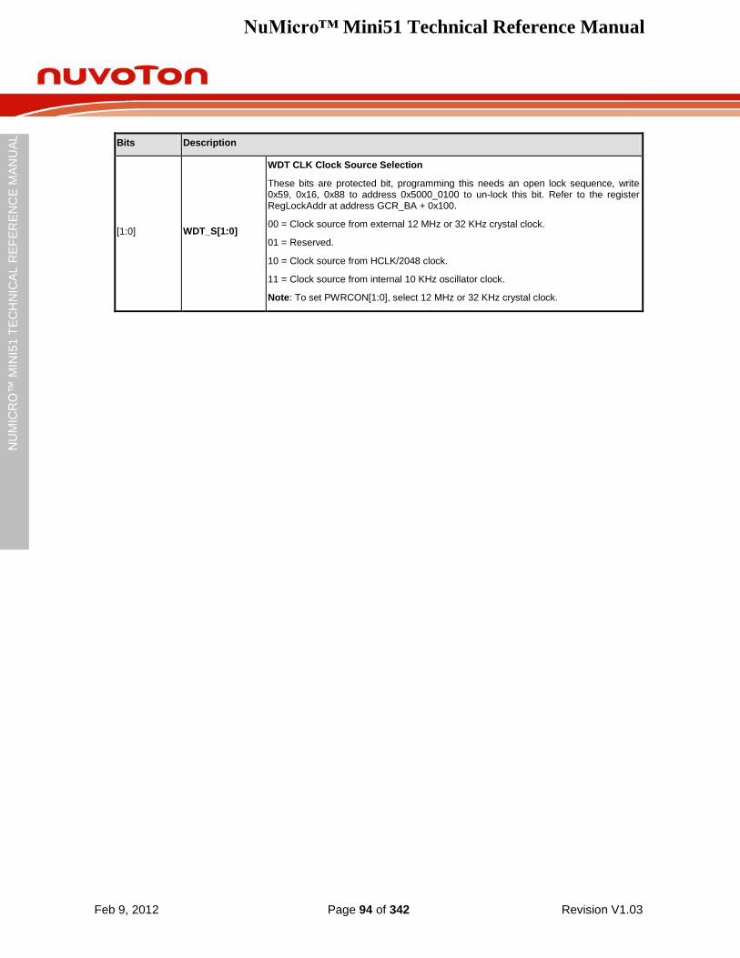
NuMicro™ Mini51 Technical Reference Manual
Feb 9, 2012 Page 94 of 342 Revision V1.03
NU
MIC
RO
™ M
INI5
1 T
EC
HN
ICA
L R
EF
ER
EN
CE
MA
NU
AL
Bits Description
[1:0] WDT_S[1:0]
WDT CLK Clock Source Selection
These bits are protected bit, programming this needs an open lock sequence, write 0x59, 0x16, 0x88 to address 0x5000_0100 to un-lock this bit. Refer to the register RegLockAddr at address GCR_BA + 0x100.
00 = Clock source from external 12 MHz or 32 KHz crystal clock.
01 = Reserved.
10 = Clock source from HCLK/2048 clock.
11 = Clock source from internal 10 KHz oscillator clock.
Note: To set PWRCON[1:0], select 12 MHz or 32 KHz crystal clock.
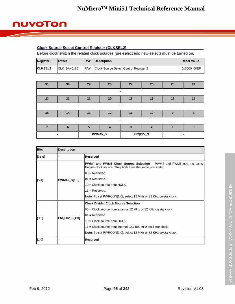
NuMicro™ Mini51 Technical Reference Manual
Feb 9, 2012 Page 95 of 342 Revision V1.03
NU
MIC
RO
™ M
INI5
1 T
EC
HN
ICA
L R
EF
ER
EN
CE
MA
NU
AL
Clock Source Select Control Register (CLKSEL2)
Before clock switch the related clock sources (pre-select and new-select) must be turned on.
Register Offset R/W Description Reset Value
CLKSEL2 CLK_BA+0x1C R/W Clock Source Select Control Register 2 0x0000_00EF
31 30 29 28 27 26 25 24
-
23 22 21 20 19 18 17 16
-
15 14 13 12 11 10 9 8
-
7 6 5 4 3 2 1 0
- PWM45_S FRQDIV_S -
Bits Description
[31:6] - Reserved
[5:4] PWM45_S[1:0]
PWM4 and PWM5 Clock Source Selection – PWM4 and PWM5 use the same Engine clock source. They both have the same pre-scalar.
00 = Reserved.
01 = Reserved.
10 = Clock source from HCLK.
11 = Reserved.
Note: To set PWRCON[1:0], select 12 MHz or 32 KHz crystal clock.
[3:2] FRQDIV_S[1:0]
Clock Divider Clock Source Selection
00 = Clock source from external 12 MHz or 32 KHz crystal clock.
01 = Reserved.
10 = Clock source from HCLK.
11 = Clock source from internal 22.1184 MHz oscillator clock.
Note: To set PWRCON[1:0], select 12 MHz or 32 KHz crystal clock.
[1:0] - Reserved
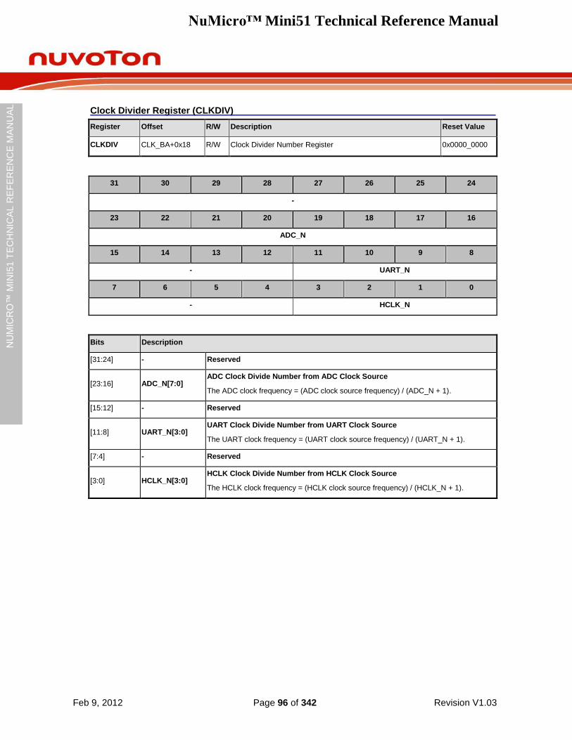
NuMicro™ Mini51 Technical Reference Manual
Feb 9, 2012 Page 96 of 342 Revision V1.03
NU
MIC
RO
™ M
INI5
1 T
EC
HN
ICA
L R
EF
ER
EN
CE
MA
NU
AL
Clock Divider Register (CLKDIV)
Register Offset R/W Description Reset Value
CLKDIV CLK_BA+0x18 R/W Clock Divider Number Register 0x0000_0000
31 30 29 28 27 26 25 24
-
23 22 21 20 19 18 17 16
ADC_N
15 14 13 12 11 10 9 8
- UART_N
7 6 5 4 3 2 1 0
- HCLK_N
Bits Description
[31:24] - Reserved
[23:16] ADC_N[7:0] ADC Clock Divide Number from ADC Clock Source
The ADC clock frequency = (ADC clock source frequency) / (ADC_N + 1).
[15:12] - Reserved
[11:8] UART_N[3:0] UART Clock Divide Number from UART Clock Source
The UART clock frequency = (UART clock source frequency) / (UART_N + 1).
[7:4] - Reserved
[3:0] HCLK_N[3:0] HCLK Clock Divide Number from HCLK Clock Source
The HCLK clock frequency = (HCLK clock source frequency) / (HCLK_N + 1).
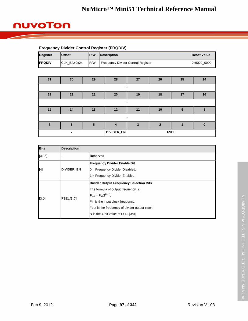
NuMicro™ Mini51 Technical Reference Manual
Feb 9, 2012 Page 97 of 342 Revision V1.03
NU
MIC
RO
™ M
INI5
1 T
EC
HN
ICA
L R
EF
ER
EN
CE
MA
NU
AL
Frequency Divider Control Register (FRQDIV)
Register Offset R/W Description Reset Value
FRQDIV CLK_BA+0x24 R/W Frequency Divider Control Register 0x0000_0000
31 30 29 28 27 26 25 24
-
23 22 21 20 19 18 17 16
-
15 14 13 12 11 10 9 8
-
7 6 5 4 3 2 1 0
- DIVIDER_EN FSEL
Bits Description
[31:5] - Reserved
[4] DIVIDER_EN
Frequency Divider Enable Bit
0 = Frequency Divider Disabled.
1 = Frequency Divider Enabled.
[3:0] FSEL[3:0]
Divider Output Frequency Selection Bits
The formula of output frequency is:
Fout = Fin/2(N+1)
,
Fin is the input clock frequency.
Fout is the frequency of divider output clock.
N is the 4-bit value of FSEL[3:0].
NuMicro™ Mini51 Technical Reference Manual
Feb 9, 2012 Page 98 of 342 Revision V1.03
NU
MIC
RO
™ M
INI5
1 T
EC
HN
ICA
L R
EF
ER
EN
CE
MA
NU
AL
5.5 Comparator Controller (CMPC)
5.5.1 Overview
The NuMicro Mini51 Series contains two comparators which can be used in a number of different configurations. The comparator output is a logical one when positive input is greater than negative input; otherwise, the output is zero. Each comparator can be configured to cause an interrupt when the comparator output value changes. The block diagram is shown in Figure 5.5-1.
Note that the analog input port pins must be configured as the input type before Analog Comparator function is enabled.
5.5.2 Features
Analog input voltage range: 0 ~ 5.0V
Hysteresis function support
Two analog comparators with optional internal reference voltage input at negative end
One comparator interrupt requested by one of the comparators
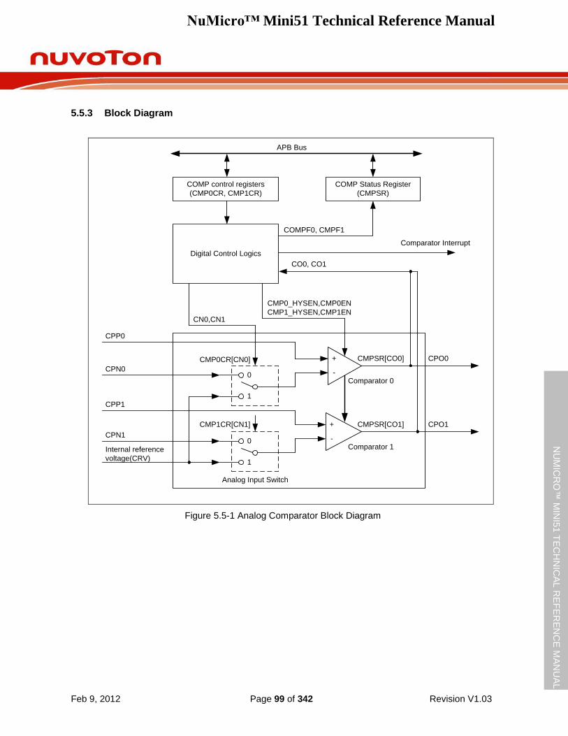
NuMicro™ Mini51 Technical Reference Manual
Feb 9, 2012 Page 99 of 342 Revision V1.03
NU
MIC
RO
™ M
INI5
1 T
EC
HN
ICA
L R
EF
ER
EN
CE
MA
NU
AL
5.5.3 Block Diagram
COMP Status Register
(CMPSR)
+
-
Digital Control Logics
CPN0
Internal reference
voltage(CRV)
Analog Input Switch
Comparator 1
Comparator Interrupt
CPP0
COMPF0, CMPF1
Comparator 0
CMPSR[CO0]
CPP1
CPN1
CN0,CN1
CMP0_HYSEN,CMP0EN
CMP1_HYSEN,CMP1EN
CMP0CR[CN0]
0
1
CMP1CR[CN1] CMPSR[CO1]
COMP control registers
(CMP0CR, CMP1CR)
APB Bus
0
1
+
-
CPO0
CPO1
CO0, CO1
Figure 5.5-1 Analog Comparator Block Diagram
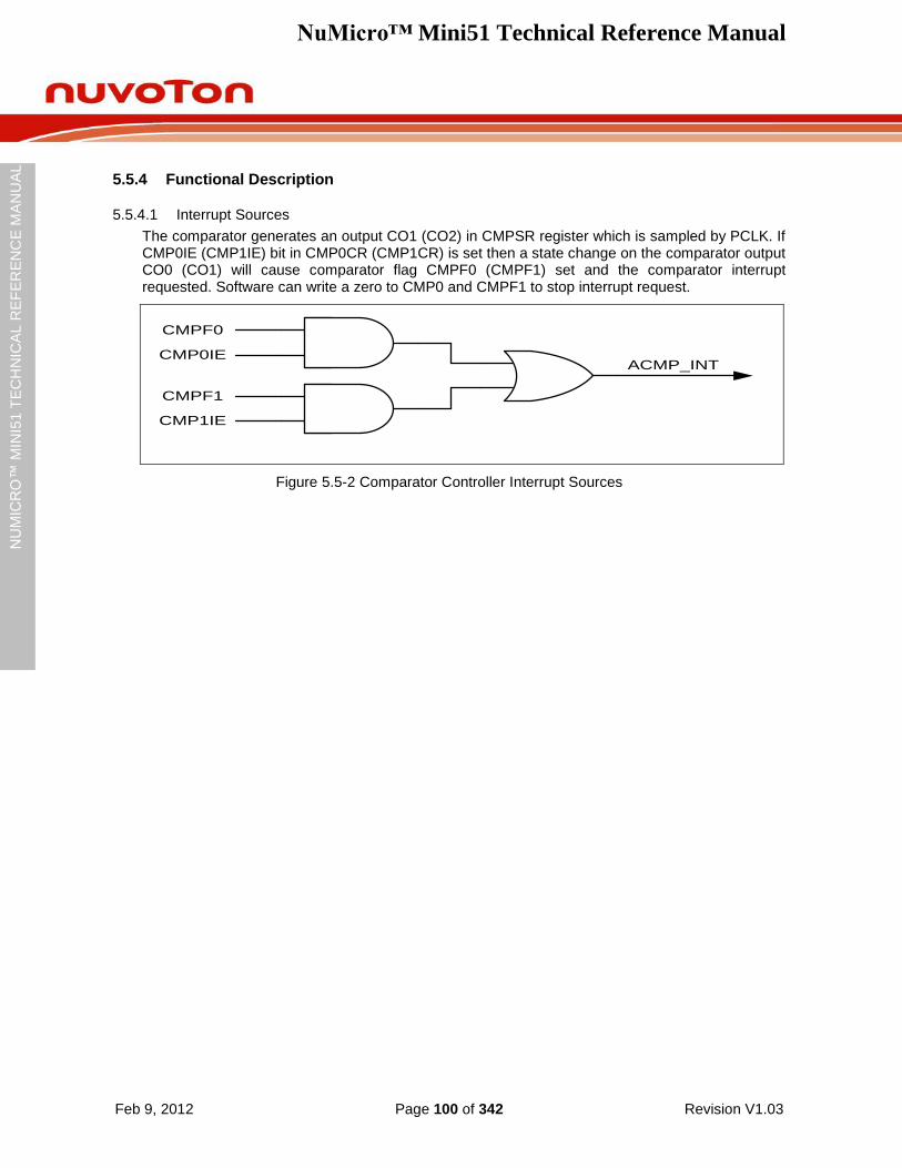
NuMicro™ Mini51 Technical Reference Manual
Feb 9, 2012 Page 100 of 342 Revision V1.03
NU
MIC
RO
™ M
INI5
1 T
EC
HN
ICA
L R
EF
ER
EN
CE
MA
NU
AL
5.5.4 Functional Description
5.5.4.1 Interrupt Sources
The comparator generates an output CO1 (CO2) in CMPSR register which is sampled by PCLK. If CMP0IE (CMP1IE) bit in CMP0CR (CMP1CR) is set then a state change on the comparator output CO0 (CO1) will cause comparator flag CMPF0 (CMPF1) set and the comparator interrupt requested. Software can write a zero to CMP0 and CMPF1 to stop interrupt request.
CMPF0
CMP0IE
CMPF1
CMP1IE
ACMP_INT
Figure 5.5-2 Comparator Controller Interrupt Sources
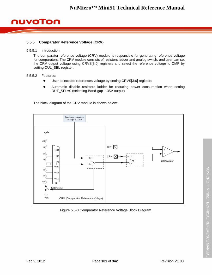
NuMicro™ Mini51 Technical Reference Manual
Feb 9, 2012 Page 101 of 342 Revision V1.03
NU
MIC
RO
™ M
INI5
1 T
EC
HN
ICA
L R
EF
ER
EN
CE
MA
NU
AL
5.5.5 Comparator Reference Voltage (CRV)
5.5.5.1 Introduction
The comparator reference voltage (CRV) module is responsible for generating reference voltage for comparators. The CRV module consists of resisters ladder and analog switch, and user can set the CRV output voltage using CRVS[3:0] registers and select the reference voltage to CMP by setting OUL_SEL register.
5.5.5.2 Features:
User selectable references voltage by setting CRVS[3:0] registers
Automatic disable resisters ladder for reducing power consumption when setting OUT_SEL=0 (selecting Band-gap 1.35V output)
The block diagram of the CRV module is shown below:
VSS
4R
R
R
R
R
4R
...
CRVS[3:0]
......
1111
1110
1101
0000
0001
0010
VDD
R
+
-
Comparator
0
1
CPP
CPN0
1
Band-gap reference
Voltage = 1.35V
CRV (Comparator Reference Volage)
Figure 5.5-3 Comparator Reference Voltage Block Diagram
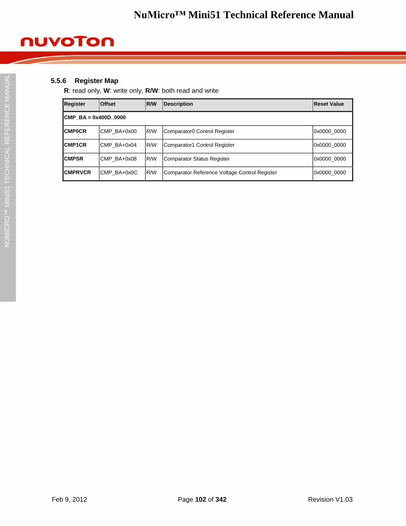
NuMicro™ Mini51 Technical Reference Manual
Feb 9, 2012 Page 102 of 342 Revision V1.03
NU
MIC
RO
™ M
INI5
1 T
EC
HN
ICA
L R
EF
ER
EN
CE
MA
NU
AL
5.5.6 Register Map
R: read only, W: write only, R/W: both read and write
Register Offset R/W Description Reset Value
CMP_BA = 0x400D_0000
CMP0CR CMP_BA+0x00 R/W Comparator0 Control Register 0x0000_0000
CMP1CR CMP_BA+0x04 R/W Comparator1 Control Register 0x0000_0000
CMPSR CMP_BA+0x08 R/W Comparator Status Register 0x0000_0000
CMPRVCR CMP_BA+0x0C R/W Comparator Reference Voltage Control Register 0x0000_0000
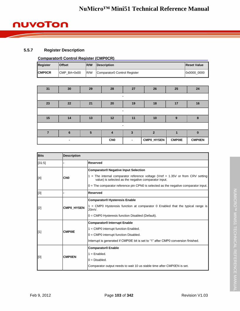
NuMicro™ Mini51 Technical Reference Manual
Feb 9, 2012 Page 103 of 342 Revision V1.03
NU
MIC
RO
™ M
INI5
1 T
EC
HN
ICA
L R
EF
ER
EN
CE
MA
NU
AL
5.5.7 Register Description
Comparator0 Control Register (CMP0CR)
Register Offset R/W Description Reset Value
CMP0CR CMP_BA+0x00 R/W Comparator0 Control Register 0x0000_0000
31 30 29 28 27 26 25 24
-
23 22 21 20 19 18 17 16
-
15 14 13 12 11 10 9 8
-
7 6 5 4 3 2 1 0
- CN0 - CMP0_HYSEN CMP0IE CMP0EN
Bits Description
[31:5] - Reserved
[4] CN0
Comparator0 Negative Input Selection
1 = The internal comparator reference voltage (Vref = 1.35V or from CRV setting value) is selected as the negative comparator input.
0 = The comparator reference pin CPN0 is selected as the negative comparator input.
[3] - Reserved
[2] CMP0_HYSEN
Comparator0 Hysteresis Enable
1 = CMP0 Hysteresis function at comparator 0 Enabled that the typical range is 20mV.
0 = CMP0 Hysteresis function Disabled (Default).
[1] CMP0IE
Comparator0 Interrupt Enable
1 = CMP0 interrupt function Enabled.
0 = CMP0 interrupt function Disabled.
Interrupt is generated if CMP0IE bit is set to “1” after CMP0 conversion finished.
[0] CMP0EN
Comparator0 Enable
1 = Enabled.
0 = Disabled.
Comparator output needs to wait 10 us stable time after CMP0EN is set.
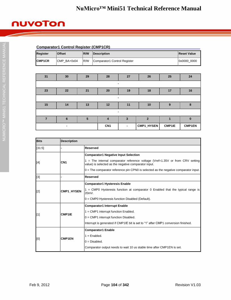
NuMicro™ Mini51 Technical Reference Manual
Feb 9, 2012 Page 104 of 342 Revision V1.03
NU
MIC
RO
™ M
INI5
1 T
EC
HN
ICA
L R
EF
ER
EN
CE
MA
NU
AL
Comparator1 Control Register (CMP1CR)
Register Offset R/W Description Reset Value
CMP1CR CMP_BA+0x04 R/W Comparator1 Control Register 0x0000_0000
31 30 29 28 27 26 25 24
-
23 22 21 20 19 18 17 16
-
15 14 13 12 11 10 9 8
-
7 6 5 4 3 2 1 0
- CN1 - CMP1_HYSEN CMP1IE CMP1EN
Bits Description
[31:5] - Reserved
[4] CN1
Comparator1 Negative Input Selection
1 = The internal comparator reference voltage (Vref=1.35V or from CRV setting value) is selected as the negative comparator input.
0 = The comparator reference pin CPN0 is selected as the negative comparator input.
[3] - Reserved
[2] CMP1_HYSEN
Comparator1 Hysteresis Enable
1 = CMP0 Hysteresis function at comparator 0 Enabled that the typical range is 20mV.
0 = CMP0 Hysteresis function Disabled (Default).
[1] CMP1IE
Comparator1 Interrupt Enable
1 = CMP1 interrupt function Enabled.
0 = CMP1 interrupt function Disabled.
Interrupt is generated if CMP1IE bit is set to “1” after CMP1 conversion finished.
[0] CMP1EN
Comparator1 Enable
1 = Enabled.
0 = Disabled.
Comparator output needs to wait 10 us stable time after CMP1EN is set.
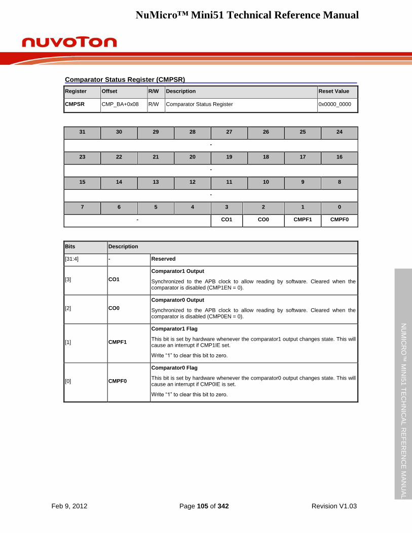
NuMicro™ Mini51 Technical Reference Manual
Feb 9, 2012 Page 105 of 342 Revision V1.03
NU
MIC
RO
™ M
INI5
1 T
EC
HN
ICA
L R
EF
ER
EN
CE
MA
NU
AL
Comparator Status Register (CMPSR)
Register Offset R/W Description Reset Value
CMPSR CMP_BA+0x08 R/W Comparator Status Register 0x0000_0000
31 30 29 28 27 26 25 24
-
23 22 21 20 19 18 17 16
-
15 14 13 12 11 10 9 8
-
7 6 5 4 3 2 1 0
- CO1 CO0 CMPF1 CMPF0
Bits Description
[31:4] - Reserved
[3] CO1
Comparator1 Output
Synchronized to the APB clock to allow reading by software. Cleared when the comparator is disabled (CMP1EN = 0).
[2] CO0
Comparator0 Output
Synchronized to the APB clock to allow reading by software. Cleared when the comparator is disabled (CMP0EN = 0).
[1] CMPF1
Comparator1 Flag
This bit is set by hardware whenever the comparator1 output changes state. This will cause an interrupt if CMP1IE set.
Write “1” to clear this bit to zero.
[0] CMPF0
Comparator0 Flag
This bit is set by hardware whenever the comparator0 output changes state. This will cause an interrupt if CMP0IE is set.
Write “1” to clear this bit to zero.
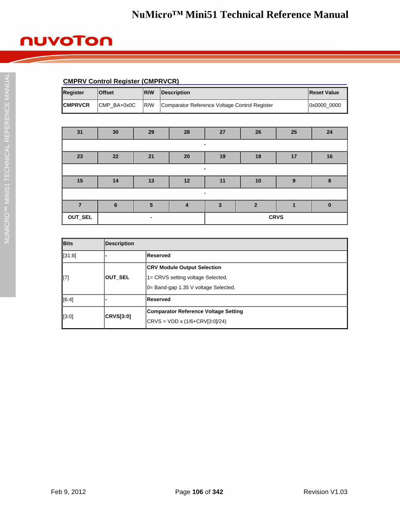
NuMicro™ Mini51 Technical Reference Manual
Feb 9, 2012 Page 106 of 342 Revision V1.03
NU
MIC
RO
™ M
INI5
1 T
EC
HN
ICA
L R
EF
ER
EN
CE
MA
NU
AL
CMPRV Control Register (CMPRVCR)
Register Offset R/W Description Reset Value
CMPRVCR CMP_BA+0x0C R/W Comparator Reference Voltage Control Register 0x0000_0000
31 30 29 28 27 26 25 24
-
23 22 21 20 19 18 17 16
-
15 14 13 12 11 10 9 8
-
7 6 5 4 3 2 1 0
OUT_SEL - CRVS
Bits Description
[31:8] - Reserved
[7] OUT_SEL
CRV Module Output Selection
1= CRVS setting voltage Selected.
0= Band-gap 1.35 V voltage Selected.
[6:4] - Reserved
[3:0] CRVS[3:0] Comparator Reference Voltage Setting
CRVS = VDD x (1/6+CRV[3:0]/24)
NuMicro™ Mini51 Technical Reference Manual
Feb 9, 2012 Page 107 of 342 Revision V1.03
NU
MIC
RO
™ M
INI5
1 T
EC
HN
ICA
L R
EF
ER
EN
CE
MA
NU
AL
5.6 Analog-to-Digital Converter (ADC) Controller
5.6.1 Overview
The NuMicro Mini51 series contains one 10-bit successive approximation analog-to-digital converters (SAR A/D converter) with 8 input channels. The A/D converters can be started by software and external STADC/P3.2 pin.
Note that the analog input pins must be configured as input type before ADC function is enabled.
5.6.2 Features
Analog input voltage range: 0 ~ Vref (Max to 5.0 V)
10-bit resolution and 8-bit accuracy is guaranteed
Up to 8 single-end analog input channels
Maximum ADC clock frequency is 6 MHz
Up to 150K SPS conversion rate
An A/D conversion is performed one time on a specified channel
An A/D conversion can be started by:
Software write “1” to ADST bit
External pin STADC
Conversion results are held in data register with valid and overrun indicators
Conversion results can be compared with specified value and user can select whether to generate an interrupt when conversion results are equal to the compare register settings
Channel 7 supports 2 input sources: External analog voltage and internal fixed band-gap voltage
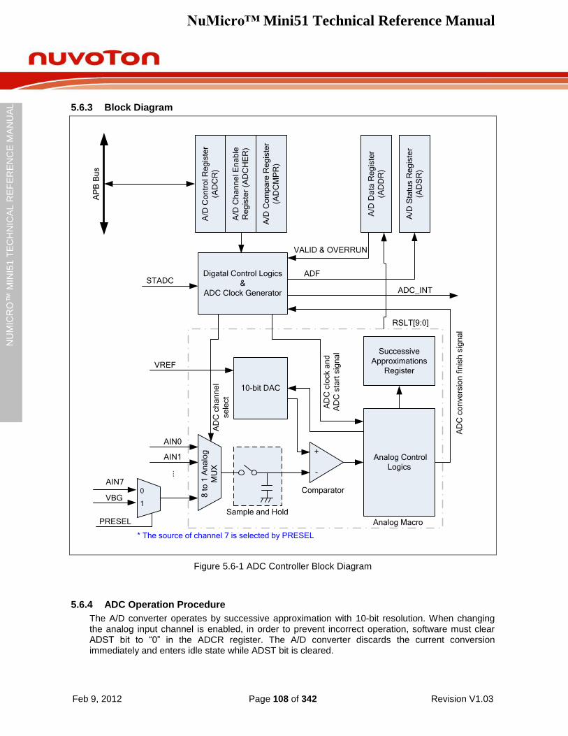
NuMicro™ Mini51 Technical Reference Manual
Feb 9, 2012 Page 108 of 342 Revision V1.03
NU
MIC
RO
™ M
INI5
1 T
EC
HN
ICA
L R
EF
ER
EN
CE
MA
NU
AL
5.6.3 Block Diagram
10-bit DAC
A/D
Sta
tus R
eg
iste
r
(AD
SR
)
Analog Control
Logics
Successive
Approximations
RegisterA
/D D
ata
Re
gis
ter
(AD
DR
)
+
-
Digatal Control Logics
&
ADC Clock Generator
A/D
Co
ntr
ol R
eg
iste
r
(AD
CR
)
A/D
Ch
an
ne
l E
na
ble
Re
gis
ter
(AD
CH
ER
)
A/D
Co
mp
are
Re
gis
ter
(AD
CM
PR
)
...
AIN0
AIN1
AIN7
8 t
o 1
An
alo
g
MU
X
Sample and Hold
Comparator
RSLT[9:0]
STADC
Analog Macro
AD
C c
lock a
nd
AD
C s
tart
sig
na
l
VREF
AD
C c
ha
nn
el
se
lect
AP
B B
us
VALID & OVERRUN
ADF
VBG0
1
PRESEL
AD
C c
on
ve
rsio
n f
inis
h s
ign
al
* The source of channel 7 is selected by PRESEL
ADC_INT
Figure 5.6-1 ADC Controller Block Diagram
5.6.4 ADC Operation Procedure
The A/D converter operates by successive approximation with 10-bit resolution. When changing the analog input channel is enabled, in order to prevent incorrect operation, software must clear ADST bit to “0” in the ADCR register. The A/D converter discards the current conversion immediately and enters idle state while ADST bit is cleared.
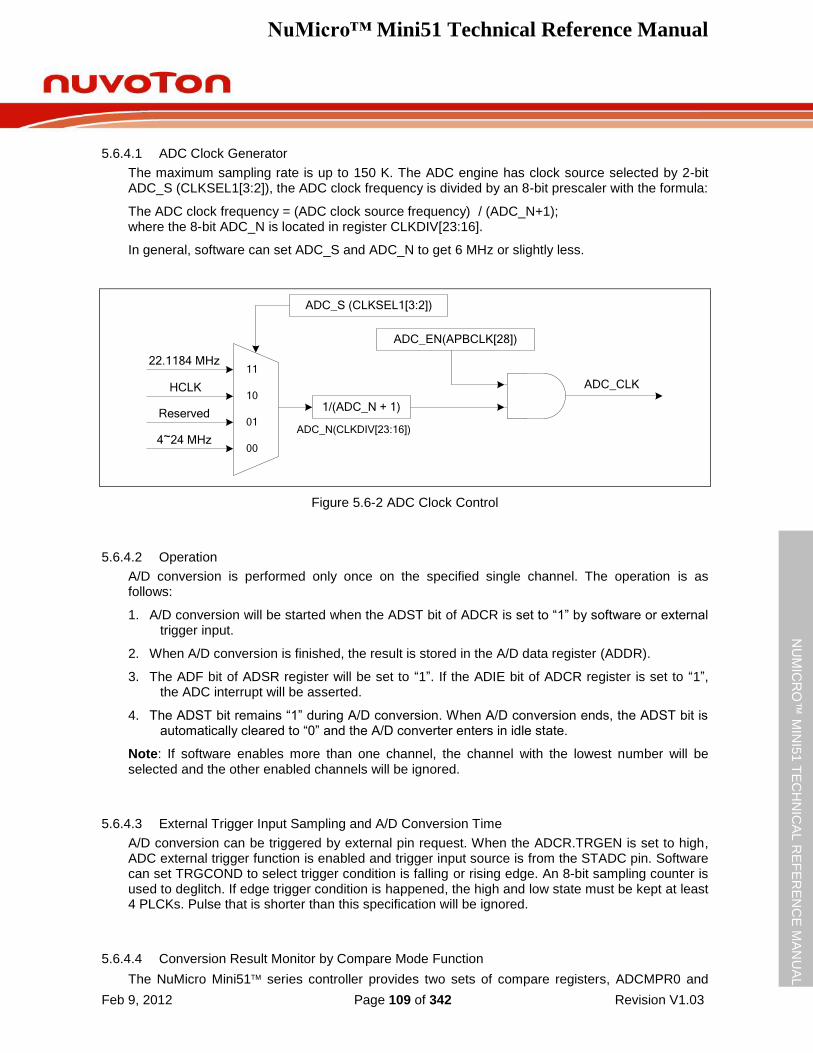
NuMicro™ Mini51 Technical Reference Manual
Feb 9, 2012 Page 109 of 342 Revision V1.03
NU
MIC
RO
™ M
INI5
1 T
EC
HN
ICA
L R
EF
ER
EN
CE
MA
NU
AL
5.6.4.1 ADC Clock Generator
The maximum sampling rate is up to 150 K. The ADC engine has clock source selected by 2-bit ADC_S (CLKSEL1[3:2]), the ADC clock frequency is divided by an 8-bit prescaler with the formula:
The ADC clock frequency = (ADC clock source frequency) / (ADC_N+1); where the 8-bit ADC_N is located in register CLKDIV[23:16].
In general, software can set ADC_S and ADC_N to get 6 MHz or slightly less.
11
10
01
00
Reserved
4~24 MHz
22.1184 MHz
ADC_S (CLKSEL1[3:2])
ADC_EN(APBCLK[28])
ADC_CLK
1/(ADC_N + 1)
ADC_N(CLKDIV[23:16])
HCLK
Figure 5.6-2 ADC Clock Control
5.6.4.2 Operation
A/D conversion is performed only once on the specified single channel. The operation is as follows:
1. A/D conversion will be started when the ADST bit of ADCR is set to “1” by software or external trigger input.
2. When A/D conversion is finished, the result is stored in the A/D data register (ADDR).
3. The ADF bit of ADSR register will be set to “1”. If the ADIE bit of ADCR register is set to “1”, the ADC interrupt will be asserted.
4. The ADST bit remains “1” during A/D conversion. When A/D conversion ends, the ADST bit is automatically cleared to “0” and the A/D converter enters in idle state.
Note: If software enables more than one channel, the channel with the lowest number will be selected and the other enabled channels will be ignored.
5.6.4.3 External Trigger Input Sampling and A/D Conversion Time
A/D conversion can be triggered by external pin request. When the ADCR.TRGEN is set to high, ADC external trigger function is enabled and trigger input source is from the STADC pin. Software can set TRGCOND to select trigger condition is falling or rising edge. An 8-bit sampling counter is used to deglitch. If edge trigger condition is happened, the high and low state must be kept at least 4 PLCKs. Pulse that is shorter than this specification will be ignored.
5.6.4.4 Conversion Result Monitor by Compare Mode Function
The NuMicro Mini51 series controller provides two sets of compare registers, ADCMPR0 and
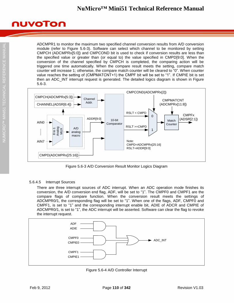
NuMicro™ Mini51 Technical Reference Manual
Feb 9, 2012 Page 110 of 342 Revision V1.03
NU
MIC
RO
™ M
INI5
1 T
EC
HN
ICA
L R
EF
ER
EN
CE
MA
NU
AL
ADCMPR1 to monitor the maximum two specified channel conversion results from A/D conversion module (refer to Figure 5.6-3). Software can select which channel to be monitored by setting CMPCH (ADCMPRx[5:0]) and CMPCOND bit is used to check if conversion results are less than the specified value or greater than (or equal to) the value specified in CMPD[9:0]. When the conversion of the channel specified by CMPCH is completed, the comparing action will be triggered one time automatically. When the compare result meets the setting, compare match counter will increase 1; otherwise, the compare match counter will be cleared to “0”. When counter value reaches the setting of (CMPMATCNT+1) the CMPF bit will be set to “1”. If CMPIE bit is set then an ADC_INT interrupt request is generated. The detailed logics diagram is shown in Figure 5.6-3.
10-bit
ComparatorRSLT >=CMPD
RSLT < CMPD
CMPCOND(ADCMPRx[2])
1
0 CMPFx
(ADSR[2:1])
A/D
analog
macro
Channel
Addr.
8 to
1
An
alo
g
MU
X
Match
Counter
CMPMATCNT
(ADCMPRx[11:8])
AIN0
AIN7
……
CHANNEL(ADSR[6:4])
CMPCH(ADCMPRx[5:3])
ADDR[9:0]
CMPD(ADCMPRx[25:16])
Note:
CMPD=ADCMPRx[25:16]
RSLT=ADDR[9:0]
Figure 5.6-3 A/D Conversion Result Monitor Logics Diagram
5.6.4.5 Interrupt Sources
There are three interrupt sources of ADC interrupt. When an ADC operation mode finishes its conversion, the A/D conversion end flag, ADF, will be set to “1”. The CMPF0 and CMPF1 are the compare flags of compare function. When the conversion result meets the settings of ADCMPR0/1, the corresponding flag will be set to “1”. When one of the flags, ADF, CMPF0 and CMPF1, is set to “1” and the corresponding interrupt enable bit, ADIE of ADCR and CMPIE of ADCMPR0/1, is set to “1”, the ADC interrupt will be asserted. Software can clear the flag to revoke the interrupt request.
ADF
ADIE
CMPF1
CMPIE1
ADC_INTCMPF0
CMPIE0
Figure 5.6-4 A/D Controller Interrupt

NuMicro™ Mini51 Technical Reference Manual
Feb 9, 2012 Page 111 of 342 Revision V1.03
NU
MIC
RO
™ M
INI5
1 T
EC
HN
ICA
L R
EF
ER
EN
CE
MA
NU
AL
5.6.5 ADC Register Map
R: read only, W: write only, R/W: both read and write
Register Offset R/W Description Reset Value
ADC_BA = 0x400E_0000
ADDR ADC_BA+0x00 R A/D Data Register 0x0000_0000
ADCR ADC_BA+0x20 R/W A/D Control Register 0x0000_0000
ADCHER ADC_BA+0x24 R/W A/D Channel Enable Register 0x0000_0000
ADCMPR0 ADC_BA+0x28 R/W A/D Compare Register 0 0x0000_0000
ADCMPR1 ADC_BA+0x2C R/W A/D Compare Register 1 0x0000_0000
ADSR ADC_BA+0x30 R/W A/D Status Register 0x0000_0000
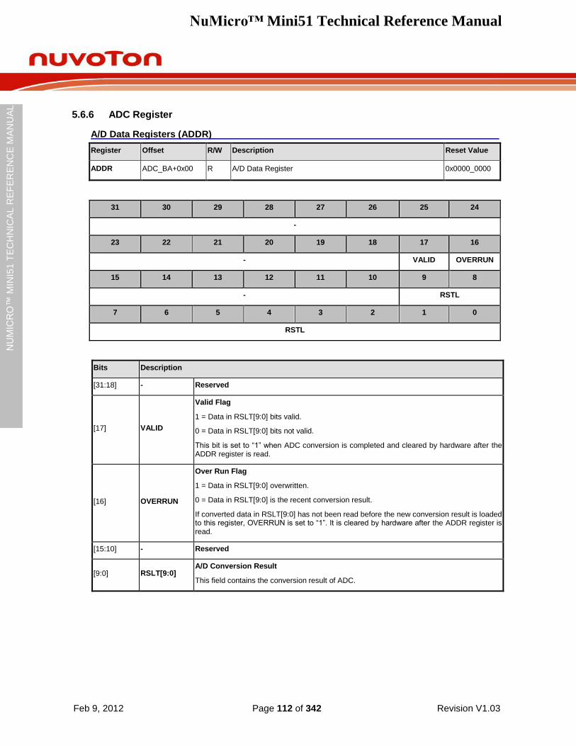
NuMicro™ Mini51 Technical Reference Manual
Feb 9, 2012 Page 112 of 342 Revision V1.03
NU
MIC
RO
™ M
INI5
1 T
EC
HN
ICA
L R
EF
ER
EN
CE
MA
NU
AL
5.6.6 ADC Register
A/D Data Registers (ADDR)
Register Offset R/W Description Reset Value
ADDR ADC_BA+0x00 R A/D Data Register 0x0000_0000
31 30 29 28 27 26 25 24
-
23 22 21 20 19 18 17 16
- VALID OVERRUN
15 14 13 12 11 10 9 8
- RSTL
7 6 5 4 3 2 1 0
RSTL
Bits Description
[31:18] - Reserved
[17] VALID
Valid Flag
1 = Data in RSLT[9:0] bits valid.
0 = Data in RSLT[9:0] bits not valid.
This bit is set to “1” when ADC conversion is completed and cleared by hardware after the ADDR register is read.
[16] OVERRUN
Over Run Flag
1 = Data in RSLT[9:0] overwritten.
0 = Data in RSLT[9:0] is the recent conversion result.
If converted data in RSLT[9:0] has not been read before the new conversion result is loaded to this register, OVERRUN is set to “1”. It is cleared by hardware after the ADDR register is read.
[15:10] - Reserved
[9:0] RSLT[9:0] A/D Conversion Result
This field contains the conversion result of ADC.
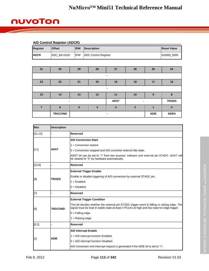
NuMicro™ Mini51 Technical Reference Manual
Feb 9, 2012 Page 113 of 342 Revision V1.03
NU
MIC
RO
™ M
INI5
1 T
EC
HN
ICA
L R
EF
ER
EN
CE
MA
NU
AL
A/D Control Register (ADCR)
Register Offset R/W Description Reset Value
ADCR ADC_BA+0x20 R/W ADC Control Register 0x0000_0000
31 30 29 28 27 26 25 24
-
23 22 21 20 19 18 17 16
-
15 14 13 12 11 10 9 8
- ADST - TRGEN
7 6 5 4 3 2 1 0
TRGCOND - ADIE ADEN
Bits Description
[31:12] - Reserved
[11] ADST
A/D Conversion Start
1 = Conversion started.
0 = Conversion stopped and A/D converter entered idle state.
ADST bit can be set to “1” from two sources: software and external pin STADC. ADST will be cleared to “0” by hardware automatically.
[10:9] - Reserved
[8] TRGEN
External Trigger Enable
Enable or disable triggering of A/D conversion by external STADC pin.
1 = Enabled.
0 = Disabled.
[7] - Reserved
[6] TRGCOND
External Trigger Condition
This bit decides whether the external pin STADC trigger event is falling or raising edge. The signal must be kept in stable state at least 4 PCLKs at high and low state for edge trigger.
0 = Falling edge.
1 = Raising edge.
[5:2] - Reserved
[1] ADIE
A/D Interrupt Enable
1 = A/D interrupt function Enabled.
0 = A/D interrupt function Disabled.
A/D conversion end interrupt request is generated if the ADIE bit is set to “1”.
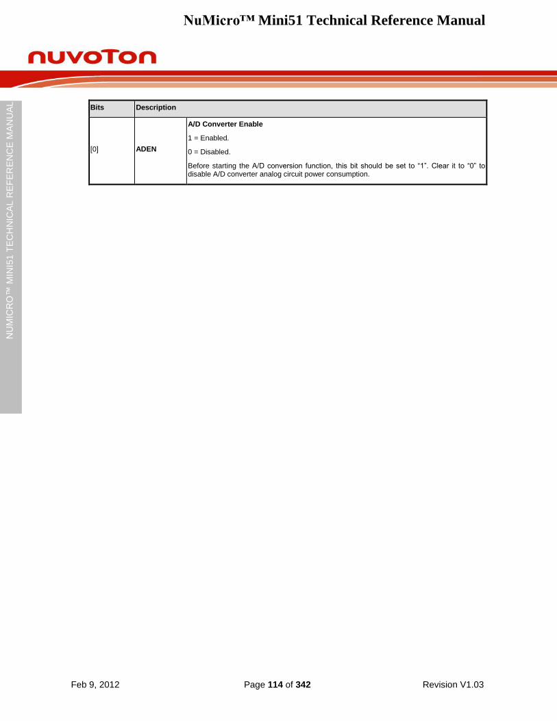
NuMicro™ Mini51 Technical Reference Manual
Feb 9, 2012 Page 114 of 342 Revision V1.03
NU
MIC
RO
™ M
INI5
1 T
EC
HN
ICA
L R
EF
ER
EN
CE
MA
NU
AL
Bits Description
[0] ADEN
A/D Converter Enable
1 = Enabled.
0 = Disabled.
Before starting the A/D conversion function, this bit should be set to “1”. Clear it to “0” to disable A/D converter analog circuit power consumption.
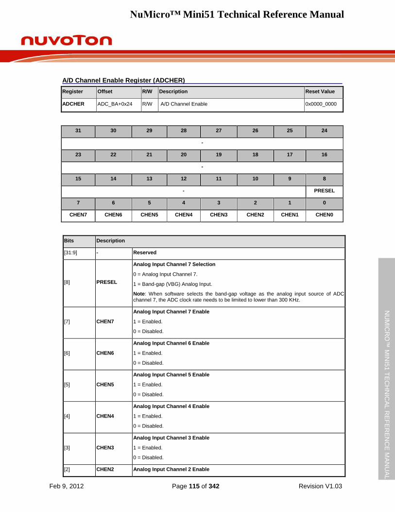
NuMicro™ Mini51 Technical Reference Manual
Feb 9, 2012 Page 115 of 342 Revision V1.03
NU
MIC
RO
™ M
INI5
1 T
EC
HN
ICA
L R
EF
ER
EN
CE
MA
NU
AL
A/D Channel Enable Register (ADCHER)
Register Offset R/W Description Reset Value
ADCHER ADC_BA+0x24 R/W A/D Channel Enable 0x0000_0000
31 30 29 28 27 26 25 24
-
23 22 21 20 19 18 17 16
-
15 14 13 12 11 10 9 8
- PRESEL
7 6 5 4 3 2 1 0
CHEN7 CHEN6 CHEN5 CHEN4 CHEN3 CHEN2 CHEN1 CHEN0
Bits Description
[31:9] - Reserved
[8] PRESEL
Analog Input Channel 7 Selection
0 = Analog Input Channel 7.
1 = Band-gap (VBG) Analog Input.
Note: When software selects the band-gap voltage as the analog input source of ADC channel 7, the ADC clock rate needs to be limited to lower than 300 KHz.
[7] CHEN7
Analog Input Channel 7 Enable
1 = Enabled.
0 = Disabled.
[6] CHEN6
Analog Input Channel 6 Enable
1 = Enabled.
0 = Disabled.
[5] CHEN5
Analog Input Channel 5 Enable
1 = Enabled.
0 = Disabled.
[4] CHEN4
Analog Input Channel 4 Enable
1 = Enabled.
0 = Disabled.
[3] CHEN3
Analog Input Channel 3 Enable
1 = Enabled.
0 = Disabled.
[2] CHEN2 Analog Input Channel 2 Enable
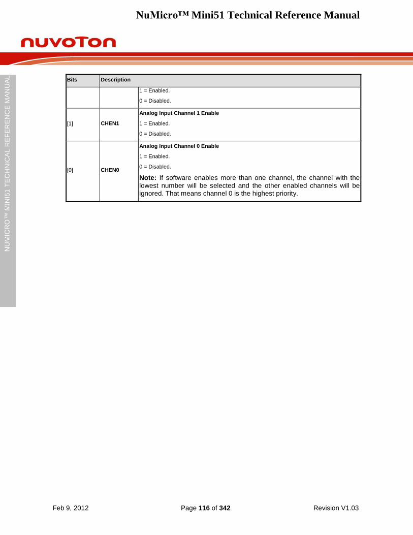
NuMicro™ Mini51 Technical Reference Manual
Feb 9, 2012 Page 116 of 342 Revision V1.03
NU
MIC
RO
™ M
INI5
1 T
EC
HN
ICA
L R
EF
ER
EN
CE
MA
NU
AL
Bits Description
1 = Enabled.
0 = Disabled.
[1] CHEN1
Analog Input Channel 1 Enable
1 = Enabled.
0 = Disabled.
[0] CHEN0
Analog Input Channel 0 Enable
1 = Enabled.
0 = Disabled.
Note: If software enables more than one channel, the channel with the lowest number will be selected and the other enabled channels will be ignored. That means channel 0 is the highest priority.
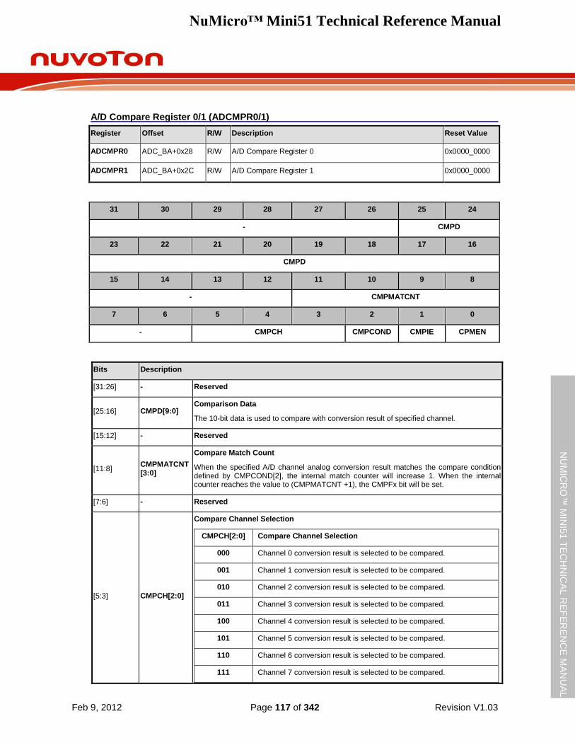
NuMicro™ Mini51 Technical Reference Manual
Feb 9, 2012 Page 117 of 342 Revision V1.03
NU
MIC
RO
™ M
INI5
1 T
EC
HN
ICA
L R
EF
ER
EN
CE
MA
NU
AL
A/D Compare Register 0/1 (ADCMPR0/1)
Register Offset R/W Description Reset Value
ADCMPR0 ADC_BA+0x28 R/W A/D Compare Register 0 0x0000_0000
ADCMPR1 ADC_BA+0x2C R/W A/D Compare Register 1 0x0000_0000
31 30 29 28 27 26 25 24
- CMPD
23 22 21 20 19 18 17 16
CMPD
15 14 13 12 11 10 9 8
- CMPMATCNT
7 6 5 4 3 2 1 0
- CMPCH CMPCOND CMPIE CPMEN
Bits Description
[31:26] - Reserved
[25:16] CMPD[9:0] Comparison Data
The 10-bit data is used to compare with conversion result of specified channel.
[15:12] - Reserved
[11:8] CMPMATCNT [3:0]
Compare Match Count
When the specified A/D channel analog conversion result matches the compare condition defined by CMPCOND[2], the internal match counter will increase 1. When the internal counter reaches the value to (CMPMATCNT +1), the CMPFx bit will be set.
[7:6] - Reserved
[5:3] CMPCH[2:0]
Compare Channel Selection
CMPCH[2:0] Compare Channel Selection
000 Channel 0 conversion result is selected to be compared.
001 Channel 1 conversion result is selected to be compared.
010 Channel 2 conversion result is selected to be compared.
011 Channel 3 conversion result is selected to be compared.
100 Channel 4 conversion result is selected to be compared.
101 Channel 5 conversion result is selected to be compared.
110 Channel 6 conversion result is selected to be compared.
111 Channel 7 conversion result is selected to be compared.
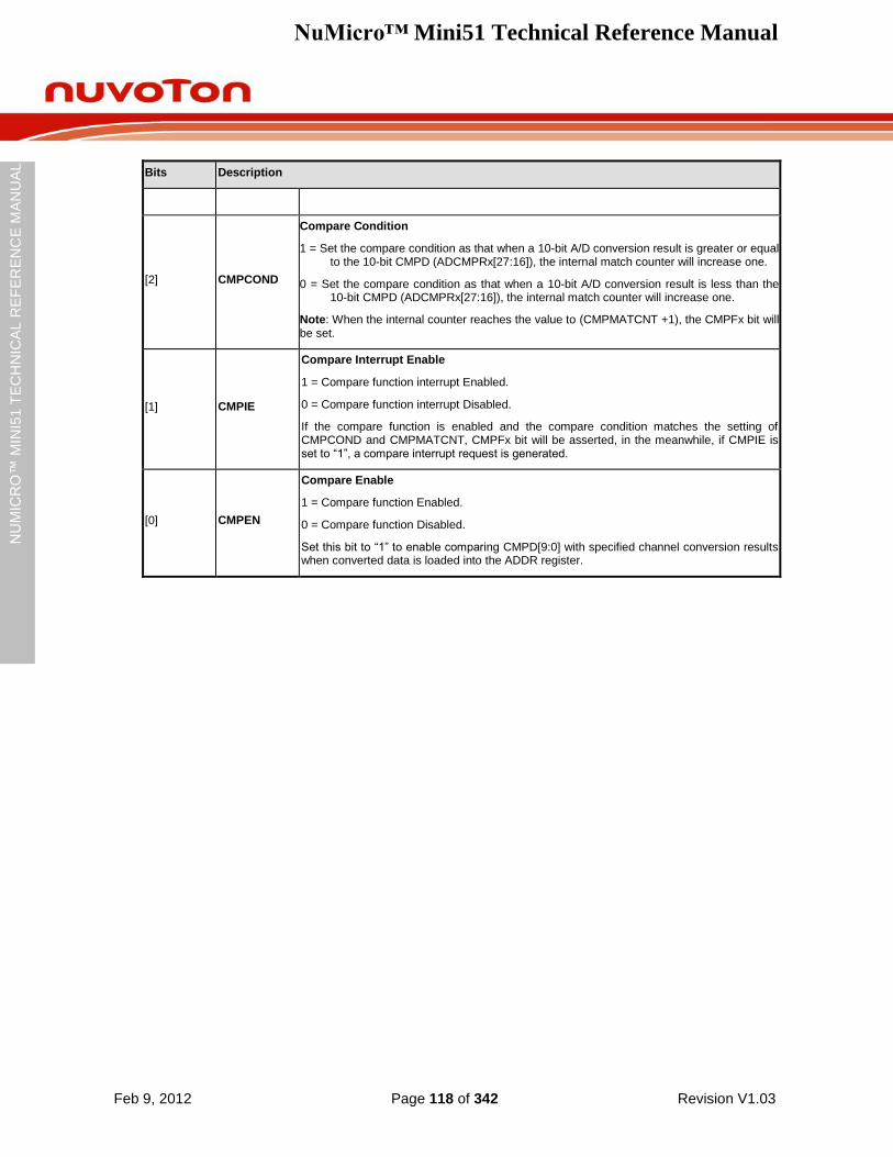
NuMicro™ Mini51 Technical Reference Manual
Feb 9, 2012 Page 118 of 342 Revision V1.03
NU
MIC
RO
™ M
INI5
1 T
EC
HN
ICA
L R
EF
ER
EN
CE
MA
NU
AL
Bits Description
[2] CMPCOND
Compare Condition
1 = Set the compare condition as that when a 10-bit A/D conversion result is greater or equal to the 10-bit CMPD (ADCMPRx[27:16]), the internal match counter will increase one.
0 = Set the compare condition as that when a 10-bit A/D conversion result is less than the 10-bit CMPD (ADCMPRx[27:16]), the internal match counter will increase one.
Note: When the internal counter reaches the value to (CMPMATCNT +1), the CMPFx bit will be set.
[1] CMPIE
Compare Interrupt Enable
1 = Compare function interrupt Enabled.
0 = Compare function interrupt Disabled.
If the compare function is enabled and the compare condition matches the setting of CMPCOND and CMPMATCNT, CMPFx bit will be asserted, in the meanwhile, if CMPIE is set to “1”, a compare interrupt request is generated.
[0] CMPEN
Compare Enable
1 = Compare function Enabled.
0 = Compare function Disabled.
Set this bit to “1” to enable comparing CMPD[9:0] with specified channel conversion results when converted data is loaded into the ADDR register.

NuMicro™ Mini51 Technical Reference Manual
Feb 9, 2012 Page 119 of 342 Revision V1.03
NU
MIC
RO
™ M
INI5
1 T
EC
HN
ICA
L R
EF
ER
EN
CE
MA
NU
AL
A/D Status Register (ADSR)
Register Offset R/W Description Reset Value
ADSR ADC_BA+0x30 R/W ADC Status Register 0x0000_0000
31 30 29 28 27 26 25 24
-
23 22 21 20 19 18 17 16
- OVERRUN
15 14 13 12 11 10 9 8
- VALID
7 6 5 4 3 2 1 0
- CHANNEL BUSY CMPF1 CMPF0 ADF
Bits Description
[31:17] - Reserved
[16] OVERRUN Over Run Flag
It is a mirror to OVERRUN bit in ADDR.
[15:9] - Reserved
[8] VALID Data Valid Flag
It is a mirror of VALID bit in ADDR.
[7] - Reserved
[6:4] CHANNEL [2:0]
Current Conversion Channel
This field reflects the current conversion channel when BUSY=1. When BUSY=0, it shows the number of the next converted channel.
It is read only.
[3] BUSY
BUSY/IDLE
1 = A/D converter is busy at conversion.
0 = A/D converter is in idle state.
This bit is mirror of as ADST bit in ADCR.
It is read only.
[2] CMPF1
Compare Flag #1
When the selected channel A/D conversion result meets the setting condition in ADCMPR1, this bit is set to “1”. Then it is cleared by writing “1” to itself.
1 = Conversion result in ADDR meets the ADCMPR1 setting.
0 = Conversion result in ADDR does not meet the ADCMPR1 setting.
[1] CMPF0 Compare Flag #0
NuMicro™ Mini51 Technical Reference Manual
Feb 9, 2012 Page 120 of 342 Revision V1.03
NU
MIC
RO
™ M
INI5
1 T
EC
HN
ICA
L R
EF
ER
EN
CE
MA
NU
AL
Bits Description
When the selected channel A/D conversion result meets the setting condition in ADCMPR0, this bit is set to “1”. Then it is cleared by writing “1” to itself.
1 = Conversion result in ADDR meets the ADCMPR0 setting.
0 = Conversion result in ADDR does not meet the ADCMPR0 setting.
[0] ADF
A/D Conversion End Flag
A status flag that indicates the end of A/D conversion.
ADF is set to “1” when A/D conversion ends.
This flag can be cleared by writing “1” to itself.

NuMicro™ Mini51 Technical Reference Manual
Feb 9, 2012 Page 121 of 342 Revision V1.03
NU
MIC
RO
™ M
INI5
1 T
EC
HN
ICA
L R
EF
ER
EN
CE
MA
NU
AL
5.7 Flash Memory Controller (FMC)
5.7.1 Overview
The NuMicro Mini51TM
series is equipped with 4K/8K/16K bytes on chip embedded Flash EPROM for application program memory (APROM) that can be updated through ISP procedure. In System Programming (ISP) function enables user to update program memory when chip is soldered on PCB. After chip powered on Cortex-M0 CPU fetches code from APROM or LDROM decided by boot select (CBS) in Config0. By the way, the NuMicro Mini51
TM series also provides DATA Flash
Region, where the data flash is shared with original program memory and its start address is configurable and defined by user in Config1. The data flash size is defined by user depending on the application request.
5.7.2 Features
Compatible with AHB interface
Running up to 24 MHz with zero wait state for discontinuous address read access
4K/8K/16KB application program memory (APROM)
2KB in system programming (ISP) loader program memory (LDROM)
Programmable data flash start address and memory size with 512 bytes page erase unit
In System Program (ISP) to update on chip Flash EPROM
5.7.3 Block Diagram
The flash memory controller consists of AHB slave interface, ISP control logic, writer interface and flash macro interface timing control logic. The block diagram of flash memory controller is shown in the following figure.
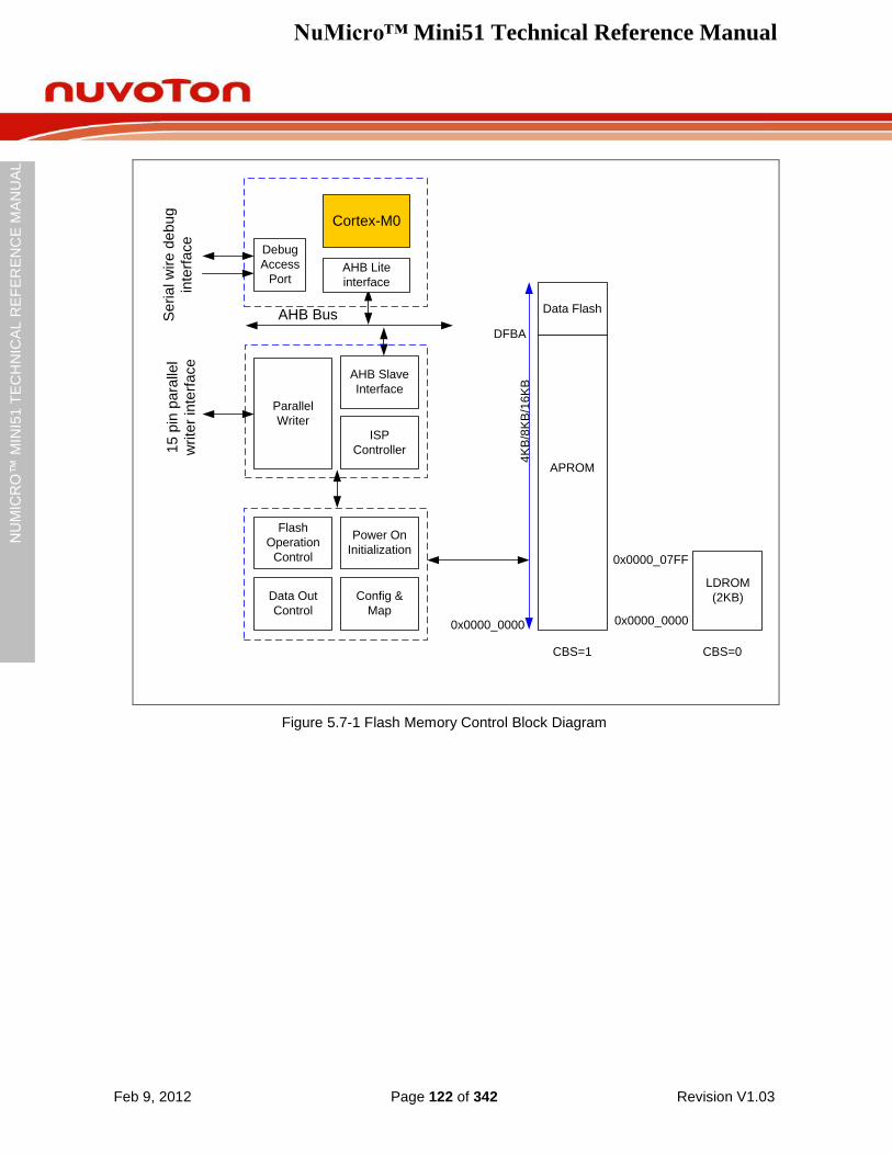
NuMicro™ Mini51 Technical Reference Manual
Feb 9, 2012 Page 122 of 342 Revision V1.03
NU
MIC
RO
™ M
INI5
1 T
EC
HN
ICA
L R
EF
ER
EN
CE
MA
NU
AL
AHB Slave
Interface
ISP
Controller
Parallel
Writer
Data Flash
0x0000_0000
Flash
Operation
Control
Power On
Initialization
Data Out
Control
Config &
Map
LDROM
(2KB)
AHB Bus
4K
B/8
KB
/16
KB
APROM
DFBA
0x0000_0000
0x0000_07FF
Cortex-M0
AHB Lite
interface
Debug
Access
Port
15
pin
pa
ralle
l
write
r in
terf
ace
Se
ria
l w
ire
de
bu
g
inte
rfa
ce
CBS=1 CBS=0
Figure 5.7-1 Flash Memory Control Block Diagram
NuMicro™ Mini51 Technical Reference Manual
Feb 9, 2012 Page 123 of 342 Revision V1.03
NU
MIC
RO
™ M
INI5
1 T
EC
HN
ICA
L R
EF
ER
EN
CE
MA
NU
AL
5.7.4 Functional Description
5.7.4.1 Flash Memory Organization
The NuMicro Mini51TM
flash memory consists of program memory (4K/8K/16KB), data flash, ISP loader program memory, and user configuration. User configuration block provides several bytes to control system logic, such as flash security lock, boot selection, Brown-out voltage level, data flash base address, and so on. It works like a fuse for power on settings. It is loaded from flash memory to its corresponding control registers during chip power on. User can set these bits according to applications requested by writer before chip is mounted on PCB. The data flash start address and its size can be defined by user depending on applications.
Table 5.7-1 Memory Address Map
Block Name Size Start Address End Address
AP-ROM ( 4-0.5*N)KB /
( 8-0.5*N)KB /
(16-0.5*N)KB
0x0000_0000 DFBA-1 (if DFEN=0)
Data Flash 0.5*N KB DFBA 0x0000_0FFF /
0x0000_1FFF /
0x0000_3FFF
Reserved for future use 0x0000_4000 0x000F_FFFF
LD-ROM 2 KB 0x0010_0000 0x0010_07FF
User Configuration 2 words 0x0030_0000 0x0030_0004
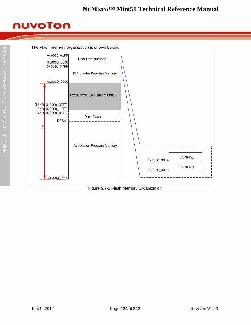
NuMicro™ Mini51 Technical Reference Manual
Feb 9, 2012 Page 124 of 342 Revision V1.03
NU
MIC
RO
™ M
INI5
1 T
EC
HN
ICA
L R
EF
ER
EN
CE
MA
NU
AL
The Flash memory organization is shown below:
User Configuration
Application Program Memory
ISP Loader Program Memory
Data Flash
0x0000_0000
0x0010_0000
Reserved for Future Used
0x0030_0000
0x0030_01FF
CONFIG0
CONFIG1
0x0030_0000
0x0030_0004
0x0010_07FF
1M
B
DFBA
(16KB) 0x0000_3FFF
( 8KB) 0x0000_1FFF
( 4KB) 0x0000_0FFF
Figure 5.7-2 Flash Memory Organization
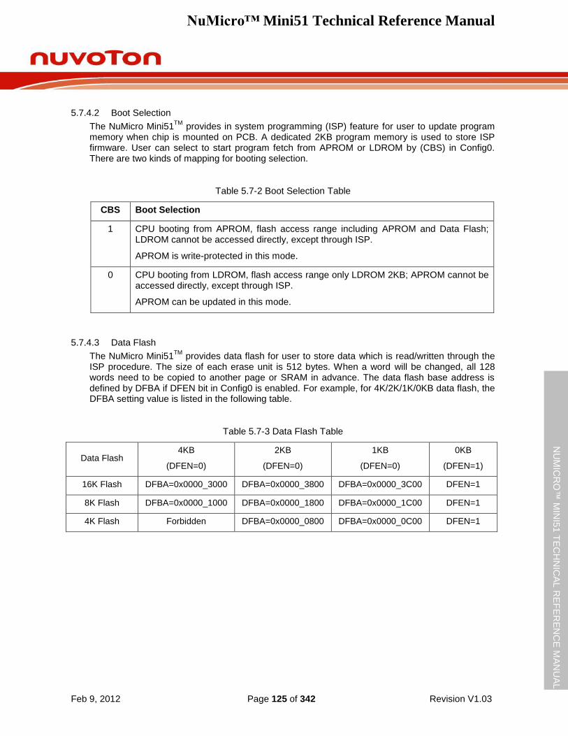
NuMicro™ Mini51 Technical Reference Manual
Feb 9, 2012 Page 125 of 342 Revision V1.03
NU
MIC
RO
™ M
INI5
1 T
EC
HN
ICA
L R
EF
ER
EN
CE
MA
NU
AL
5.7.4.2 Boot Selection
The NuMicro Mini51TM
provides in system programming (ISP) feature for user to update program memory when chip is mounted on PCB. A dedicated 2KB program memory is used to store ISP firmware. User can select to start program fetch from APROM or LDROM by (CBS) in Config0. There are two kinds of mapping for booting selection.
Table 5.7-2 Boot Selection Table
CBS Boot Selection
1 CPU booting from APROM, flash access range including APROM and Data Flash; LDROM cannot be accessed directly, except through ISP.
APROM is write-protected in this mode.
0 CPU booting from LDROM, flash access range only LDROM 2KB; APROM cannot be accessed directly, except through ISP.
APROM can be updated in this mode.
5.7.4.3 Data Flash
The NuMicro Mini51TM
provides data flash for user to store data which is read/written through the ISP procedure. The size of each erase unit is 512 bytes. When a word will be changed, all 128 words need to be copied to another page or SRAM in advance. The data flash base address is defined by DFBA if DFEN bit in Config0 is enabled. For example, for 4K/2K/1K/0KB data flash, the DFBA setting value is listed in the following table.
Table 5.7-3 Data Flash Table
Data Flash 4KB
(DFEN=0)
2KB
(DFEN=0)
1KB
(DFEN=0)
0KB
(DFEN=1)
16K Flash DFBA=0x0000_3000 DFBA=0x0000_3800 DFBA=0x0000_3C00 DFEN=1
8K Flash DFBA=0x0000_1000 DFBA=0x0000_1800 DFBA=0x0000_1C00 DFEN=1
4K Flash Forbidden DFBA=0x0000_0800 DFBA=0x0000_0C00 DFEN=1
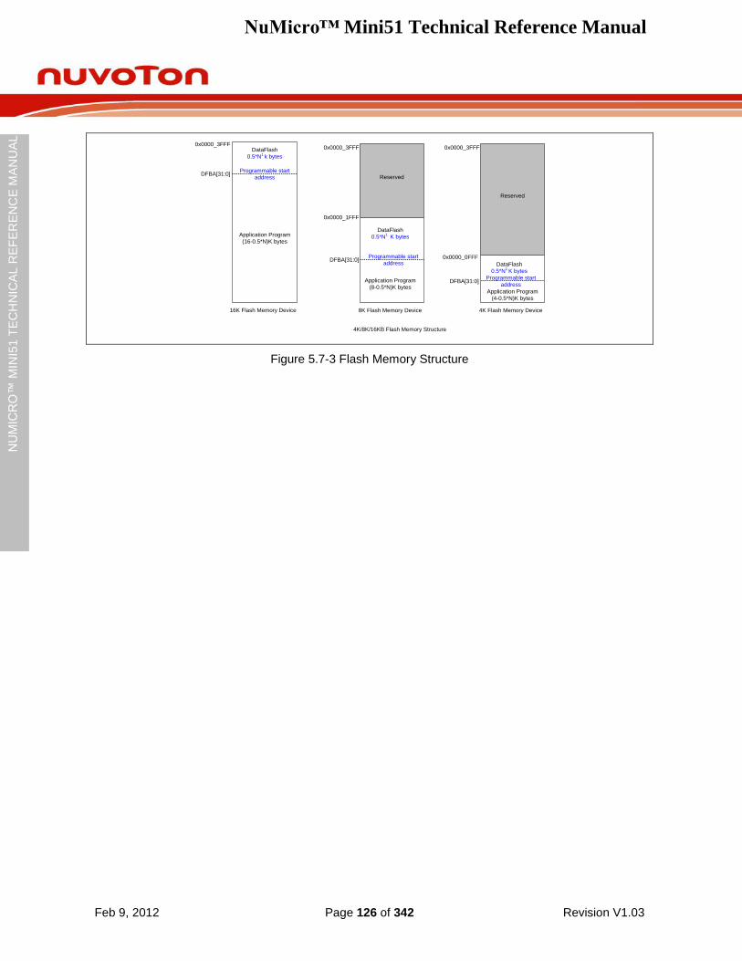
NuMicro™ Mini51 Technical Reference Manual
Feb 9, 2012 Page 126 of 342 Revision V1.03
NU
MIC
RO
™ M
INI5
1 T
EC
HN
ICA
L R
EF
ER
EN
CE
MA
NU
AL
16K Flash Memory Device
Reserved Programmable start
address
Application Program
(16-0.5*N)K bytes
4K/8K/16KB Flash Memory Structure
DFBA[31:0]
0x0000_3FFFDataFlash
0.5*N1 k bytes
8K Flash Memory Device
Programmable start
address
Application Program
(8-0.5*N)K bytes
DFBA[31:0]
0x0000_1FFF
DataFlash
0.5*N1 K bytes
0x0000_3FFF
Reserved
4K Flash Memory Device
Programmable start
address
Application Program
(4-0.5*N)K bytes
DFBA[31:0]
0x0000_0FFF
DataFlash
0.5*N1 K bytes
0x0000_3FFF
Figure 5.7-3 Flash Memory Structure
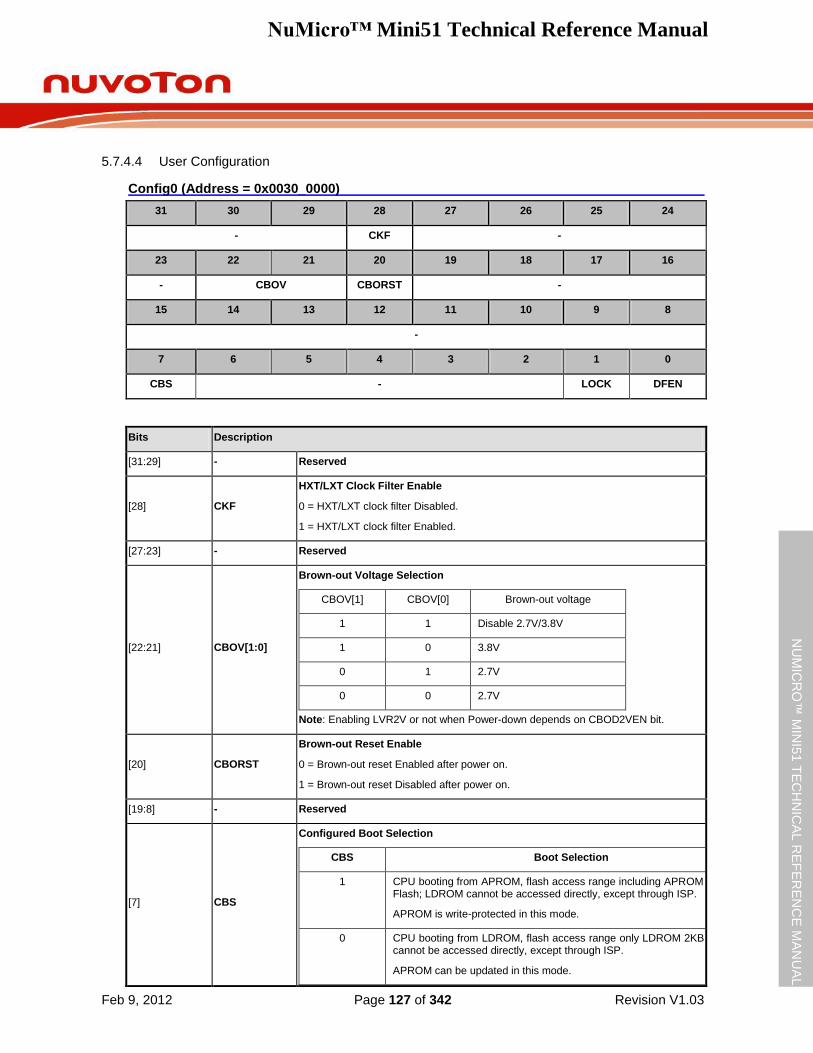
NuMicro™ Mini51 Technical Reference Manual
Feb 9, 2012 Page 127 of 342 Revision V1.03
NU
MIC
RO
™ M
INI5
1 T
EC
HN
ICA
L R
EF
ER
EN
CE
MA
NU
AL
5.7.4.4 User Configuration
Config0 (Address = 0x0030_0000)
31 30 29 28 27 26 25 24
- CKF -
23 22 21 20 19 18 17 16
- CBOV CBORST -
15 14 13 12 11 10 9 8
-
7 6 5 4 3 2 1 0
CBS - LOCK DFEN
Bits Description
[31:29] - Reserved
[28] CKF
HXT/LXT Clock Filter Enable
0 = HXT/LXT clock filter Disabled.
1 = HXT/LXT clock filter Enabled.
[27:23] - Reserved
[22:21] CBOV[1:0]
Brown-out Voltage Selection
CBOV[1] CBOV[0] Brown-out voltage
1 1 Disable 2.7V/3.8V
1 0 3.8V
0 1 2.7V
0 0 2.7V
Note: Enabling LVR2V or not when Power-down depends on CBOD2VEN bit.
[20] CBORST
Brown-out Reset Enable
0 = Brown-out reset Enabled after power on.
1 = Brown-out reset Disabled after power on.
[19:8] - Reserved
[7] CBS
Configured Boot Selection
CBS Boot Selection
1 CPU booting from APROM, flash access range including APROM and Data Flash; LDROM cannot be accessed directly, except through ISP.
APROM is write-protected in this mode.
0 CPU booting from LDROM, flash access range only LDROM 2KB; APROM cannot be accessed directly, except through ISP.
APROM can be updated in this mode.
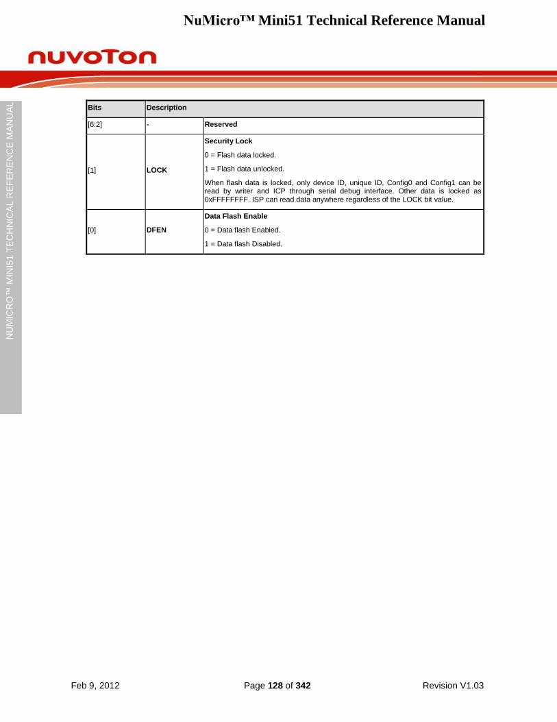
NuMicro™ Mini51 Technical Reference Manual
Feb 9, 2012 Page 128 of 342 Revision V1.03
NU
MIC
RO
™ M
INI5
1 T
EC
HN
ICA
L R
EF
ER
EN
CE
MA
NU
AL
Bits Description
[6:2] - Reserved
[1] LOCK
Security Lock
0 = Flash data locked.
1 = Flash data unlocked.
When flash data is locked, only device ID, unique ID, Config0 and Config1 can be read by writer and ICP through serial debug interface. Other data is locked as 0xFFFFFFFF. ISP can read data anywhere regardless of the LOCK bit value.
[0] DFEN
Data Flash Enable
0 = Data flash Enabled.
1 = Data flash Disabled.
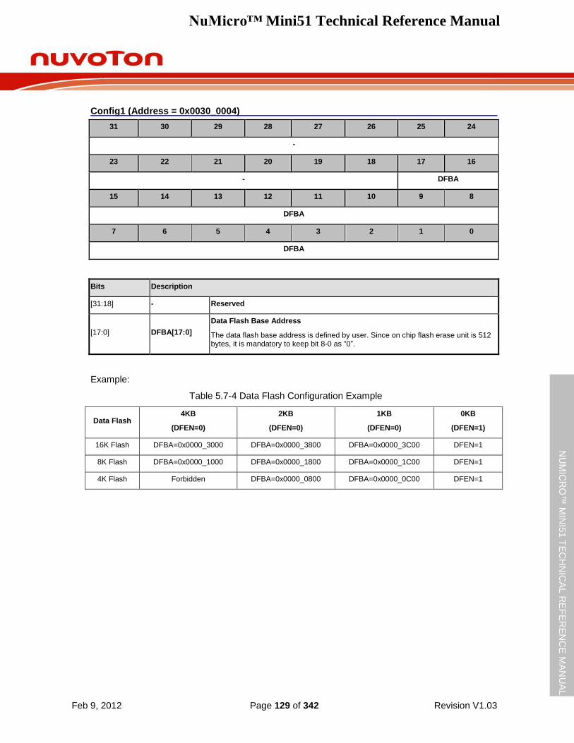
NuMicro™ Mini51 Technical Reference Manual
Feb 9, 2012 Page 129 of 342 Revision V1.03
NU
MIC
RO
™ M
INI5
1 T
EC
HN
ICA
L R
EF
ER
EN
CE
MA
NU
AL
Config1 (Address = 0x0030_0004)
31 30 29 28 27 26 25 24
-
23 22 21 20 19 18 17 16
- DFBA
15 14 13 12 11 10 9 8
DFBA
7 6 5 4 3 2 1 0
DFBA
Bits Description
[31:18] - Reserved
[17:0] DFBA[17:0]
Data Flash Base Address
The data flash base address is defined by user. Since on chip flash erase unit is 512 bytes, it is mandatory to keep bit 8-0 as “0”.
Example:
Table 5.7-4 Data Flash Configuration Example
Data Flash 4KB
(DFEN=0)
2KB
(DFEN=0)
1KB
(DFEN=0)
0KB
(DFEN=1)
16K Flash DFBA=0x0000_3000 DFBA=0x0000_3800 DFBA=0x0000_3C00 DFEN=1
8K Flash DFBA=0x0000_1000 DFBA=0x0000_1800 DFBA=0x0000_1C00 DFEN=1
4K Flash Forbidden DFBA=0x0000_0800 DFBA=0x0000_0C00 DFEN=1
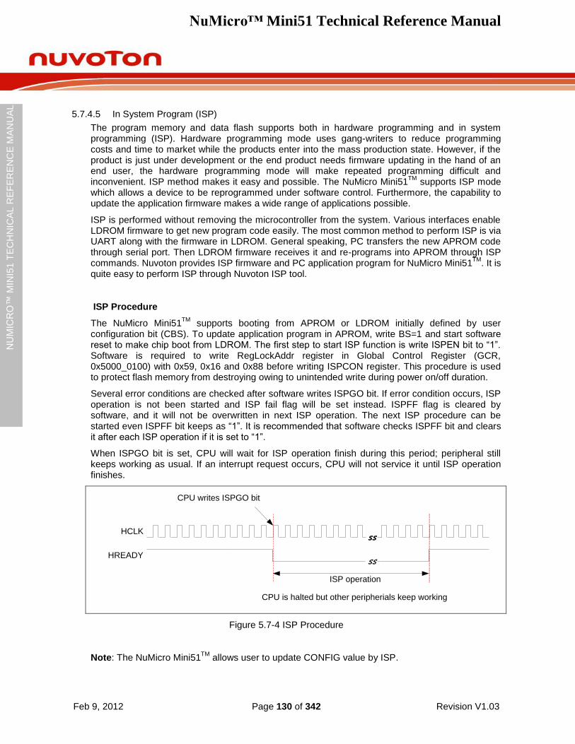
NuMicro™ Mini51 Technical Reference Manual
Feb 9, 2012 Page 130 of 342 Revision V1.03
NU
MIC
RO
™ M
INI5
1 T
EC
HN
ICA
L R
EF
ER
EN
CE
MA
NU
AL
5.7.4.5 In System Program (ISP)
The program memory and data flash supports both in hardware programming and in system programming (ISP). Hardware programming mode uses gang-writers to reduce programming costs and time to market while the products enter into the mass production state. However, if the product is just under development or the end product needs firmware updating in the hand of an end user, the hardware programming mode will make repeated programming difficult and inconvenient. ISP method makes it easy and possible. The NuMicro Mini51
TM supports ISP mode
which allows a device to be reprogrammed under software control. Furthermore, the capability to update the application firmware makes a wide range of applications possible.
ISP is performed without removing the microcontroller from the system. Various interfaces enable LDROM firmware to get new program code easily. The most common method to perform ISP is via UART along with the firmware in LDROM. General speaking, PC transfers the new APROM code through serial port. Then LDROM firmware receives it and re-programs into APROM through ISP commands. Nuvoton provides ISP firmware and PC application program for NuMicro Mini51
TM. It is
quite easy to perform ISP through Nuvoton ISP tool.
ISP Procedure
The NuMicro Mini51TM
supports booting from APROM or LDROM initially defined by user configuration bit (CBS). To update application program in APROM, write BS=1 and start software reset to make chip boot from LDROM. The first step to start ISP function is write ISPEN bit to “1”. Software is required to write RegLockAddr register in Global Control Register (GCR, 0x5000_0100) with 0x59, 0x16 and 0x88 before writing ISPCON register. This procedure is used to protect flash memory from destroying owing to unintended write during power on/off duration.
Several error conditions are checked after software writes ISPGO bit. If error condition occurs, ISP operation is not been started and ISP fail flag will be set instead. ISPFF flag is cleared by software, and it will not be overwritten in next ISP operation. The next ISP procedure can be started even ISPFF bit keeps as “1”. It is recommended that software checks ISPFF bit and clears it after each ISP operation if it is set to “1”.
When ISPGO bit is set, CPU will wait for ISP operation finish during this period; peripheral still keeps working as usual. If an interrupt request occurs, CPU will not service it until ISP operation finishes.
CPU writes ISPGO bit
ISP operation
HCLK
HREADY
CPU is halted but other peripherials keep working
ss
ss
Figure 5.7-4 ISP Procedure
Note: The NuMicro Mini51TM
allows user to update CONFIG value by ISP.
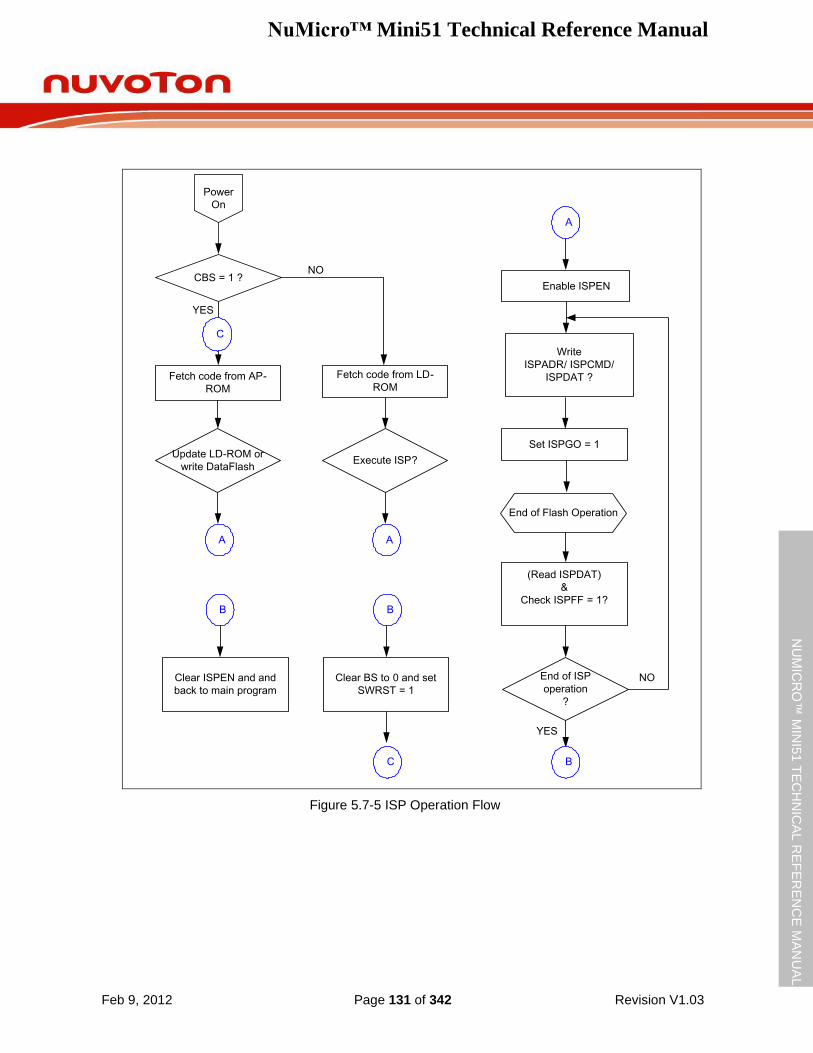
NuMicro™ Mini51 Technical Reference Manual
Feb 9, 2012 Page 131 of 342 Revision V1.03
NU
MIC
RO
™ M
INI5
1 T
EC
HN
ICA
L R
EF
ER
EN
CE
MA
NU
AL
Power
On
CBS = 1 ?
Fetch code from AP-
ROM
Fetch code from LD-
ROM
Execute ISP?
Enable ISPEN
Set ISPGO = 1
End of ISP
operation
?
(Read ISPDAT)
&
Check ISPFF = 1?
YES
YES
NO
B
Update LD-ROM or
write DataFlash
End of Flash Operation
A
A
Clear BS to 0 and set
SWRST = 1
C
C
B
A
B
Clear ISPEN and and
back to main program
NO
Write
ISPADR/ ISPCMD/
ISPDAT ?
Figure 5.7-5 ISP Operation Flow
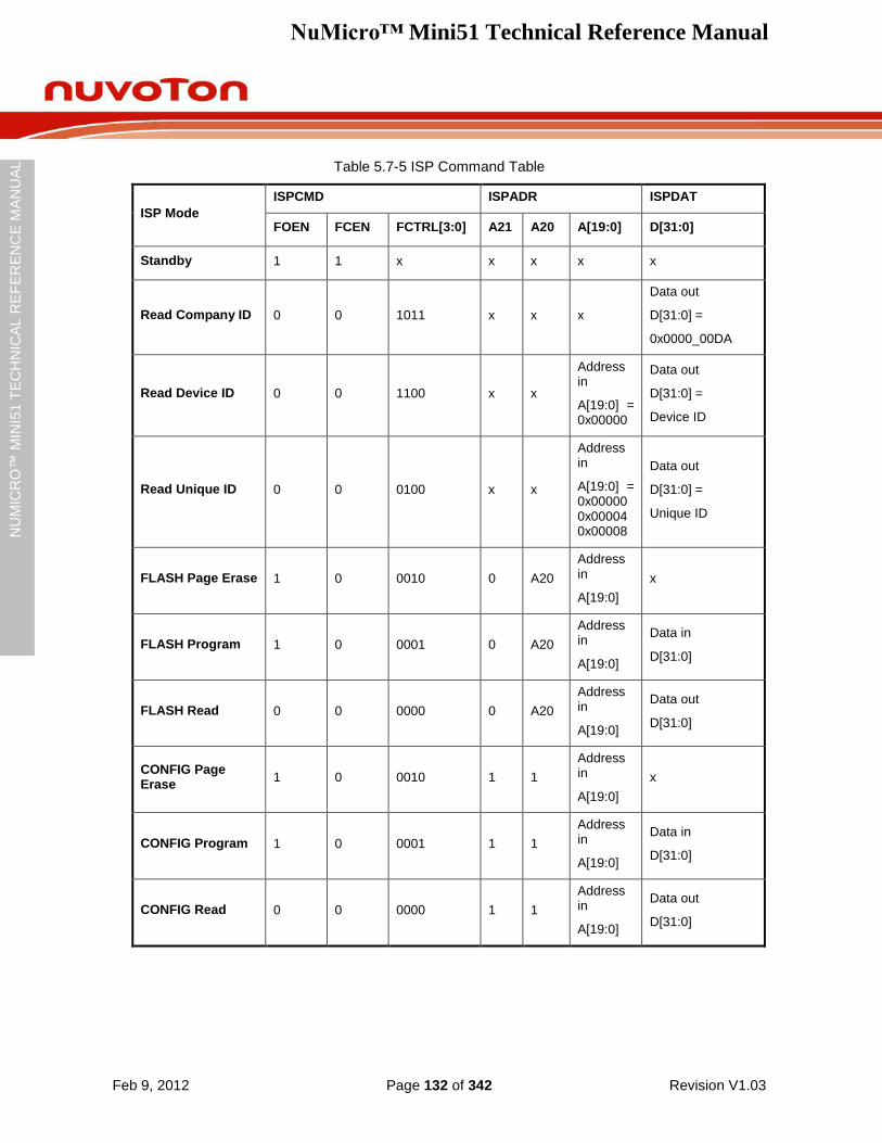
NuMicro™ Mini51 Technical Reference Manual
Feb 9, 2012 Page 132 of 342 Revision V1.03
NU
MIC
RO
™ M
INI5
1 T
EC
HN
ICA
L R
EF
ER
EN
CE
MA
NU
AL
Table 5.7-5 ISP Command Table
ISP Mode
ISPCMD ISPADR ISPDAT
FOEN FCEN FCTRL[3:0] A21 A20 A[19:0] D[31:0]
Standby 1 1 x x x x x
Read Company ID 0 0 1011 x x x
Data out
D[31:0] =
0x0000_00DA
Read Device ID 0 0 1100 x x
Address in
A[19:0] = 0x00000
Data out
D[31:0] =
Device ID
Read Unique ID 0 0 0100 x x
Address in
A[19:0] = 0x00000 0x00004 0x00008
Data out
D[31:0] =
Unique ID
FLASH Page Erase 1 0 0010 0 A20
Address in
A[19:0]
x
FLASH Program 1 0 0001 0 A20
Address in
A[19:0]
Data in
D[31:0]
FLASH Read 0 0 0000 0 A20
Address in
A[19:0]
Data out
D[31:0]
CONFIG Page Erase
1 0 0010 1 1
Address in
A[19:0]
x
CONFIG Program 1 0 0001 1 1
Address in
A[19:0]
Data in
D[31:0]
CONFIG Read 0 0 0000 1 1
Address in
A[19:0]
Data out
D[31:0]
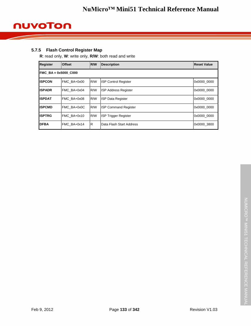
NuMicro™ Mini51 Technical Reference Manual
Feb 9, 2012 Page 133 of 342 Revision V1.03
NU
MIC
RO
™ M
INI5
1 T
EC
HN
ICA
L R
EF
ER
EN
CE
MA
NU
AL
5.7.5 Flash Control Register Map
R: read only, W: write only, R/W: both read and write
Register Offset R/W Description Reset Value
FMC_BA = 0x5000_C000
ISPCON FMC_BA+0x00 R/W ISP Control Register 0x0000_0000
ISPADR FMC_BA+0x04 R/W ISP Address Register 0x0000_0000
ISPDAT FMC_BA+0x08 R/W ISP Data Register 0x0000_0000
ISPCMD FMC_BA+0x0C R/W ISP Command Register 0x0000_0000
ISPTRG FMC_BA+0x10 R/W ISP Trigger Register 0x0000_0000
DFBA FMC_BA+0x14 R Data Flash Start Address 0x0000_3800
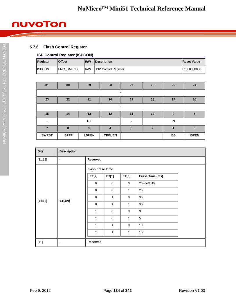
NuMicro™ Mini51 Technical Reference Manual
Feb 9, 2012 Page 134 of 342 Revision V1.03
NU
MIC
RO
™ M
INI5
1 T
EC
HN
ICA
L R
EF
ER
EN
CE
MA
NU
AL
5.7.6 Flash Control Register
ISP Control Register (ISPCON)
Register Offset R/W Description Reset Value
ISPCON FMC_BA+0x00 R/W ISP Control Register 0x0000_0000
31 30 29 28 27 26 25 24
-
23 22 21 20 19 18 17 16
-
15 14 13 12 11 10 9 8
- ET - PT
7 6 5 4 3 2 1 0
SWRST ISPFF LDUEN CFGUEN BS ISPEN
Bits Description
[31:15] - Reserved
[14:12] ET[2:0]
Flash Erase Time
ET[2] ET[1] ET[0] Erase Time (ms)
0 0 0 20 (default)
0 0 1 25
0 1 0 30
0 1 1 35
1 0 0 3
1 0 1 5
1 1 0 10
1 1 1 15
[11] - Reserved
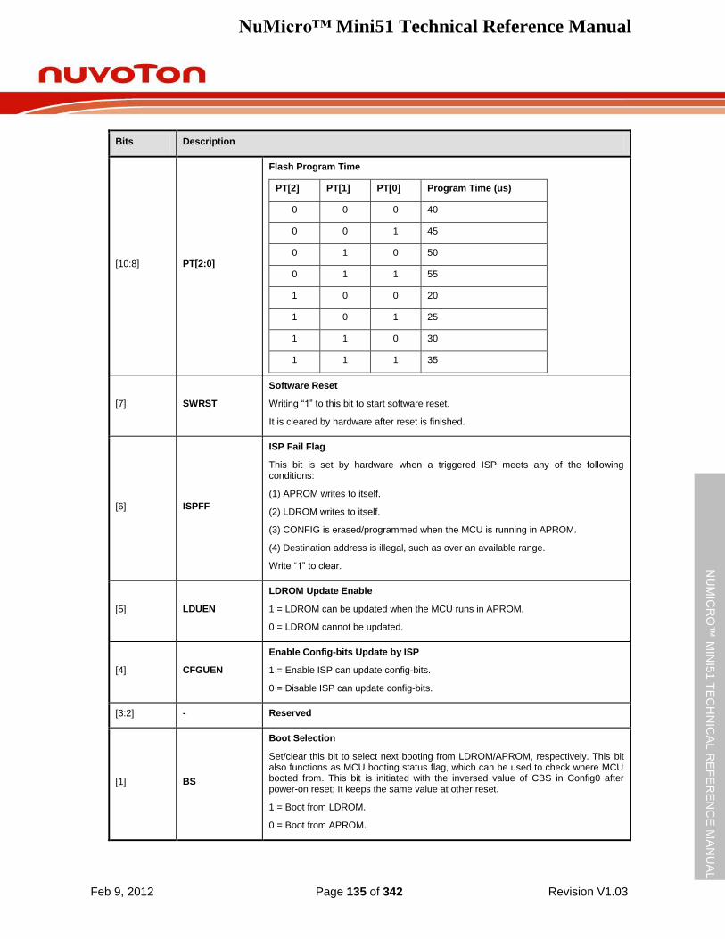
NuMicro™ Mini51 Technical Reference Manual
Feb 9, 2012 Page 135 of 342 Revision V1.03
NU
MIC
RO
™ M
INI5
1 T
EC
HN
ICA
L R
EF
ER
EN
CE
MA
NU
AL
Bits Description
[10:8] PT[2:0]
Flash Program Time
PT[2] PT[1] PT[0] Program Time (us)
0 0 0 40
0 0 1 45
0 1 0 50
0 1 1 55
1 0 0 20
1 0 1 25
1 1 0 30
1 1 1 35
[7] SWRST
Software Reset
Writing “1” to this bit to start software reset.
It is cleared by hardware after reset is finished.
[6] ISPFF
ISP Fail Flag
This bit is set by hardware when a triggered ISP meets any of the following conditions:
(1) APROM writes to itself.
(2) LDROM writes to itself.
(3) CONFIG is erased/programmed when the MCU is running in APROM.
(4) Destination address is illegal, such as over an available range.
Write “1” to clear.
[5] LDUEN
LDROM Update Enable
1 = LDROM can be updated when the MCU runs in APROM.
0 = LDROM cannot be updated.
[4] CFGUEN
Enable Config-bits Update by ISP
1 = Enable ISP can update config-bits.
0 = Disable ISP can update config-bits.
[3:2] - Reserved
[1] BS
Boot Selection
Set/clear this bit to select next booting from LDROM/APROM, respectively. This bit also functions as MCU booting status flag, which can be used to check where MCU booted from. This bit is initiated with the inversed value of CBS in Config0 after power-on reset; It keeps the same value at other reset.
1 = Boot from LDROM.
0 = Boot from APROM.
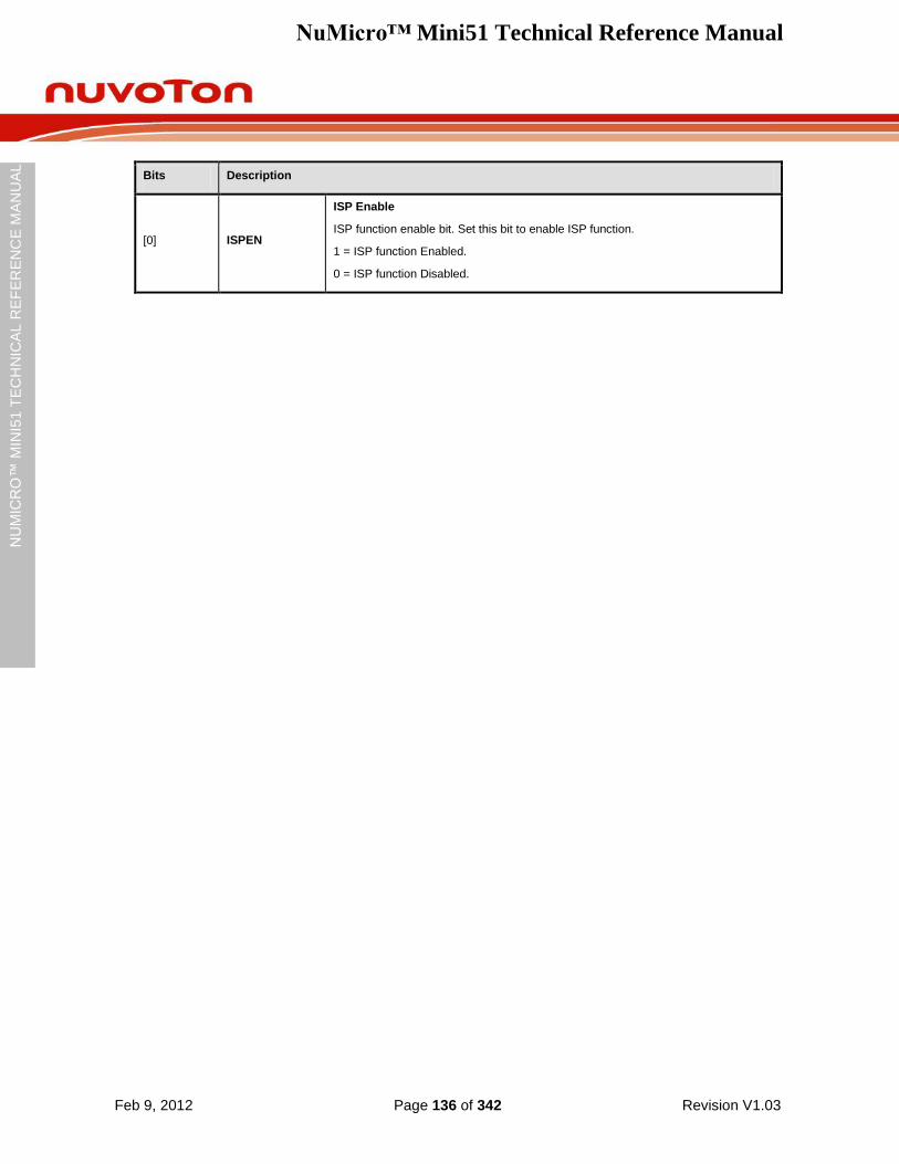
NuMicro™ Mini51 Technical Reference Manual
Feb 9, 2012 Page 136 of 342 Revision V1.03
NU
MIC
RO
™ M
INI5
1 T
EC
HN
ICA
L R
EF
ER
EN
CE
MA
NU
AL
Bits Description
[0] ISPEN
ISP Enable
ISP function enable bit. Set this bit to enable ISP function.
1 = ISP function Enabled.
0 = ISP function Disabled.
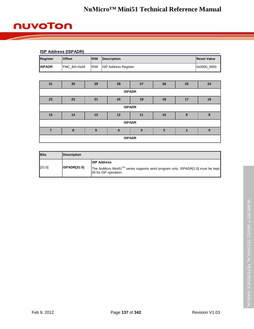
NuMicro™ Mini51 Technical Reference Manual
Feb 9, 2012 Page 137 of 342 Revision V1.03
NU
MIC
RO
™ M
INI5
1 T
EC
HN
ICA
L R
EF
ER
EN
CE
MA
NU
AL
ISP Address (ISPADR)
Register Offset R/W Description Reset Value
ISPADR FMC_BA+0x04 R/W ISP Address Register 0x0000_0000
31 30 29 28 27 26 25 24
ISPADR
23 22 21 20 19 18 17 16
ISPADR
15 14 13 12 11 10 9 8
ISPADR
7 6 5 4 3 2 1 0
ISPADR
Bits Description
[31:0] ISPADR[31:0]
ISP Address
The NuMicro Mini51TM
series supports word program only. ISPADR[1:0] must be kept 00 for ISP operation.
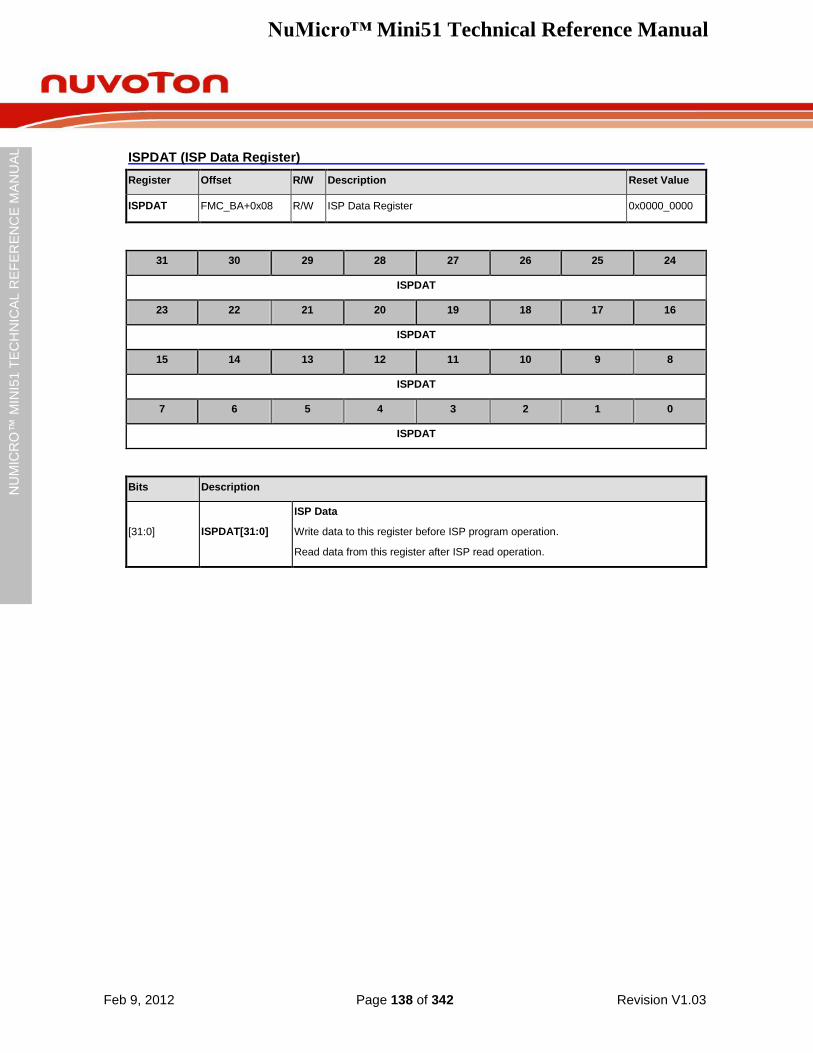
NuMicro™ Mini51 Technical Reference Manual
Feb 9, 2012 Page 138 of 342 Revision V1.03
NU
MIC
RO
™ M
INI5
1 T
EC
HN
ICA
L R
EF
ER
EN
CE
MA
NU
AL
ISPDAT (ISP Data Register)
Register Offset R/W Description Reset Value
ISPDAT FMC_BA+0x08 R/W ISP Data Register 0x0000_0000
31 30 29 28 27 26 25 24
ISPDAT
23 22 21 20 19 18 17 16
ISPDAT
15 14 13 12 11 10 9 8
ISPDAT
7 6 5 4 3 2 1 0
ISPDAT
Bits Description
[31:0] ISPDAT[31:0]
ISP Data
Write data to this register before ISP program operation.
Read data from this register after ISP read operation.
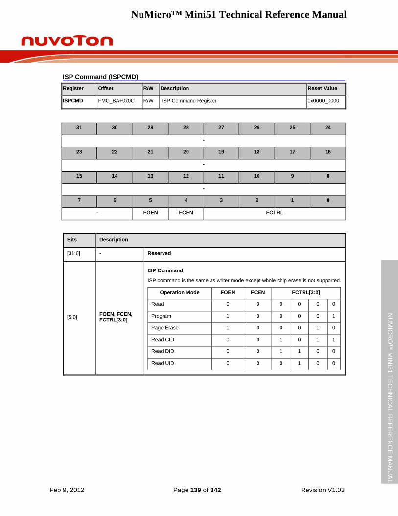
NuMicro™ Mini51 Technical Reference Manual
Feb 9, 2012 Page 139 of 342 Revision V1.03
NU
MIC
RO
™ M
INI5
1 T
EC
HN
ICA
L R
EF
ER
EN
CE
MA
NU
AL
ISP Command (ISPCMD)
Register Offset R/W Description Reset Value
ISPCMD FMC_BA+0x0C R/W ISP Command Register 0x0000_0000
31 30 29 28 27 26 25 24
-
23 22 21 20 19 18 17 16
-
15 14 13 12 11 10 9 8
-
7 6 5 4 3 2 1 0
- FOEN FCEN FCTRL
Bits Description
[31:6] - Reserved
[5:0] FOEN, FCEN, FCTRL[3:0]
ISP Command
ISP command is the same as writer mode except whole chip erase is not supported.
Operation Mode FOEN FCEN FCTRL[3:0]
Read 0 0 0 0 0 0
Program 1 0 0 0 0 1
Page Erase 1 0 0 0 1 0
Read CID 0 0 1 0 1 1
Read DID 0 0 1 1 0 0
Read UID 0 0 0 1 0 0
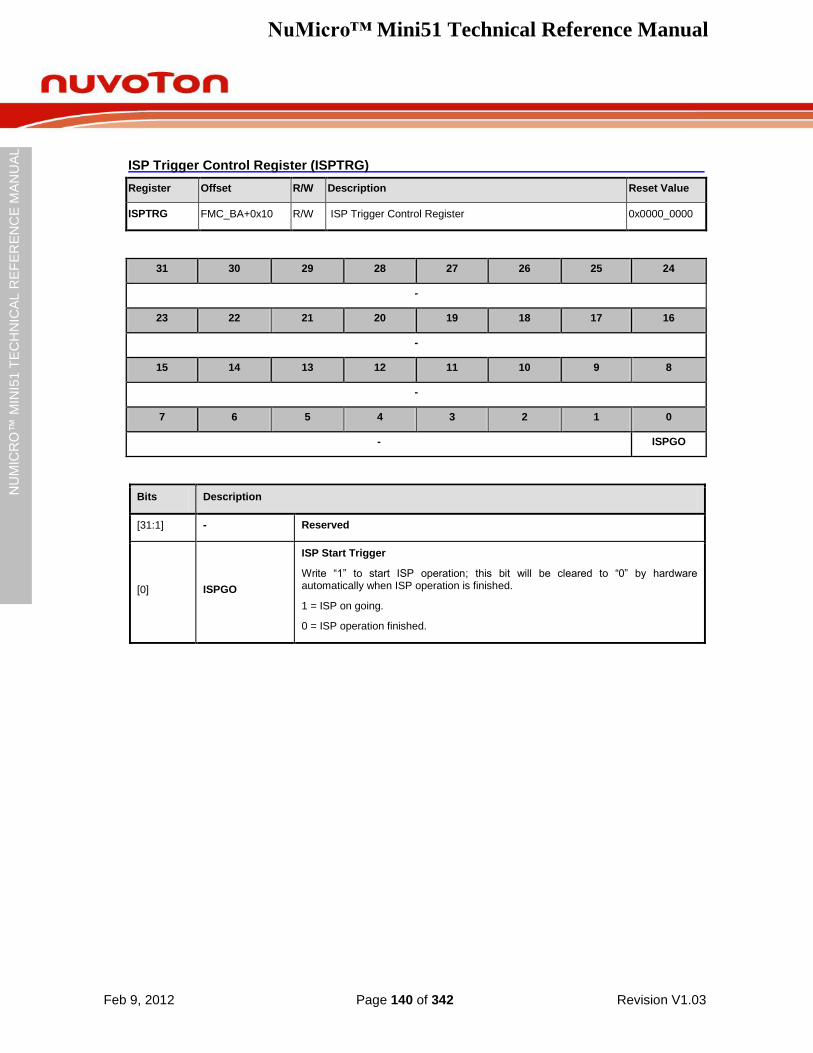
NuMicro™ Mini51 Technical Reference Manual
Feb 9, 2012 Page 140 of 342 Revision V1.03
NU
MIC
RO
™ M
INI5
1 T
EC
HN
ICA
L R
EF
ER
EN
CE
MA
NU
AL
ISP Trigger Control Register (ISPTRG)
Register Offset R/W Description Reset Value
ISPTRG FMC_BA+0x10 R/W ISP Trigger Control Register 0x0000_0000
31 30 29 28 27 26 25 24
-
23 22 21 20 19 18 17 16
-
15 14 13 12 11 10 9 8
-
7 6 5 4 3 2 1 0
- ISPGO
Bits Description
[31:1] - Reserved
[0] ISPGO
ISP Start Trigger
Write “1” to start ISP operation; this bit will be cleared to “0” by hardware automatically when ISP operation is finished.
1 = ISP on going.
0 = ISP operation finished.

NuMicro™ Mini51 Technical Reference Manual
Feb 9, 2012 Page 141 of 342 Revision V1.03
NU
MIC
RO
™ M
INI5
1 T
EC
HN
ICA
L R
EF
ER
EN
CE
MA
NU
AL
Data Flash Base Address Register (DFBA)
Register Offset R/W Description Reset Value
DFBA FMC_BA+0x14 R Data flash Base Address 0x0000_3800
31 30 29 28 27 26 25 24
DFBA
23 22 21 20 19 18 17 16
DFBA
15 14 13 12 11 10 9 8
DFBA
7 6 5 4 3 2 1 0
DFBA
Bits Description
[31:0] DFBA[31:0]
Data Flash Base Address
This register indicates data flash start address. It is a read only register.
The data flash start address is defined by user. Since on chip flash erase unit is 512 bytes, it is mandatory to keep bit 8-0 as “0”.
Example:
Data Flash 4KB (DFEN=0) 2KB (DFEN=0) 1KB (DFEN=0) 0KB (DFEN=1)
16K Flash DFBA=0x0000_3000 DFBA=0x0000_3800 DFBA=0x0000_3C00 DFEN=1
8K Flash DFBA=0x0000_1000 DFBA=0x0000_1800 DFBA=0x0000_1C00 DFEN=1
4K Flash Forbidden DFBA=0x0000_0800 DFBA=0x0000_0C00 DFEN=1
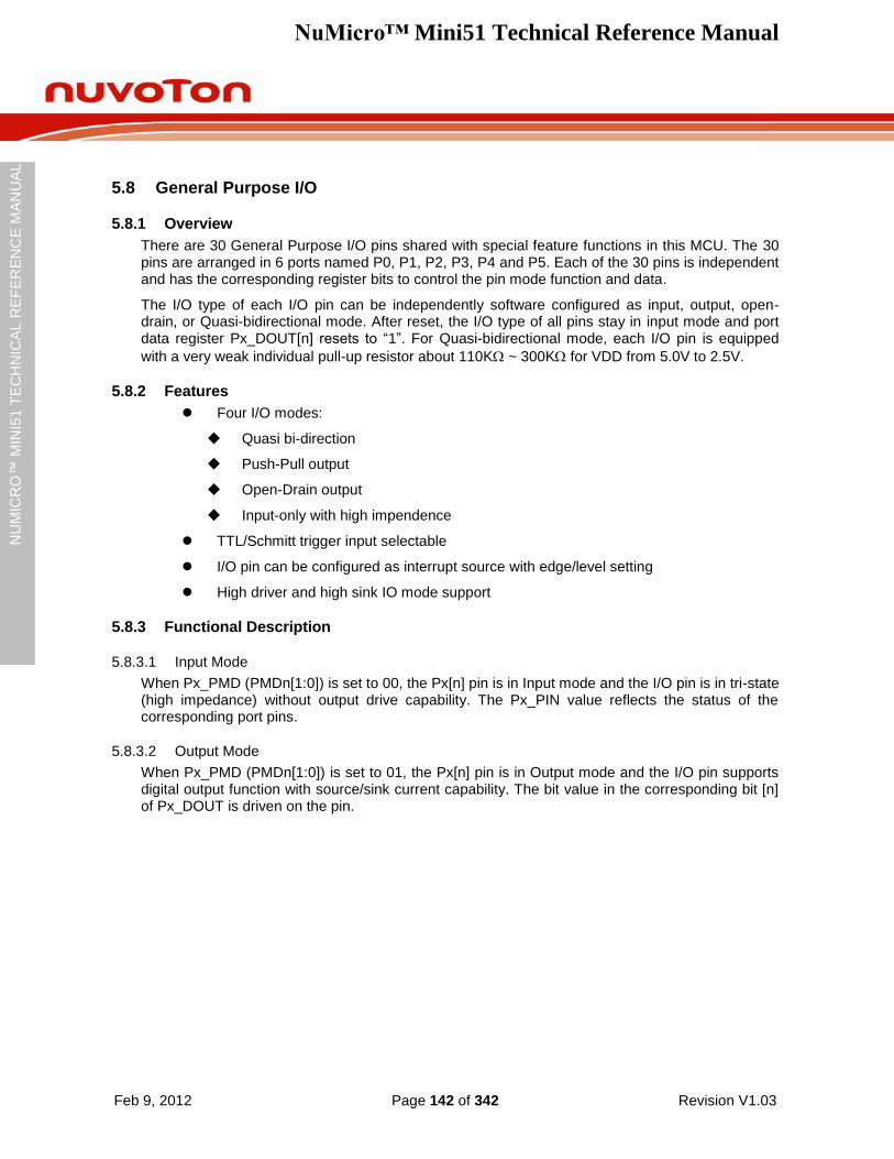
NuMicro™ Mini51 Technical Reference Manual
Feb 9, 2012 Page 142 of 342 Revision V1.03
NU
MIC
RO
™ M
INI5
1 T
EC
HN
ICA
L R
EF
ER
EN
CE
MA
NU
AL
5.8 General Purpose I/O
5.8.1 Overview
There are 30 General Purpose I/O pins shared with special feature functions in this MCU. The 30 pins are arranged in 6 ports named P0, P1, P2, P3, P4 and P5. Each of the 30 pins is independent and has the corresponding register bits to control the pin mode function and data.
The I/O type of each I/O pin can be independently software configured as input, output, open-drain, or Quasi-bidirectional mode. After reset, the I/O type of all pins stay in input mode and port data register Px_DOUT[n] resets to “1”. For Quasi-bidirectional mode, each I/O pin is equipped
with a very weak individual pull-up resistor about 110K ~ 300K for VDD from 5.0V to 2.5V.
5.8.2 Features
Four I/O modes:
Quasi bi-direction
Push-Pull output
Open-Drain output
Input-only with high impendence
TTL/Schmitt trigger input selectable
I/O pin can be configured as interrupt source with edge/level setting
High driver and high sink IO mode support
5.8.3 Functional Description
5.8.3.1 Input Mode
When Px_PMD (PMDn[1:0]) is set to 00, the Px[n] pin is in Input mode and the I/O pin is in tri-state (high impedance) without output drive capability. The Px_PIN value reflects the status of the corresponding port pins.
5.8.3.2 Output Mode
When Px_PMD (PMDn[1:0]) is set to 01, the Px[n] pin is in Output mode and the I/O pin supports digital output function with source/sink current capability. The bit value in the corresponding bit [n] of Px_DOUT is driven on the pin.
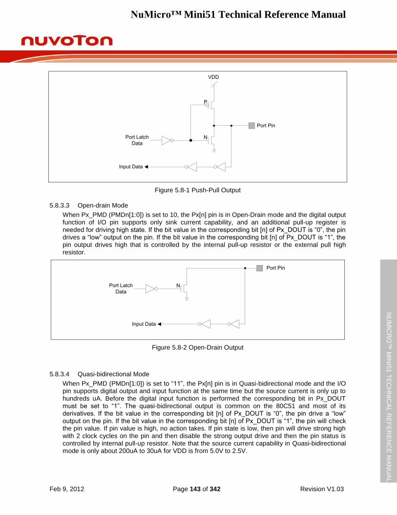
NuMicro™ Mini51 Technical Reference Manual
Feb 9, 2012 Page 143 of 342 Revision V1.03
NU
MIC
RO
™ M
INI5
1 T
EC
HN
ICA
L R
EF
ER
EN
CE
MA
NU
AL
Port Pin
Input Data
Port Latch
Data
P
N
VDD
Figure 5.8-1 Push-Pull Output
5.8.3.3 Open-drain Mode
When Px_PMD (PMDn[1:0]) is set to 10, the Px[n] pin is in Open-Drain mode and the digital output function of I/O pin supports only sink current capability, and an additional pull-up register is needed for driving high state. If the bit value in the corresponding bit [n] of Px_DOUT is “0”, the pin drives a “low” output on the pin. If the bit value in the corresponding bit [n] of Px_DOUT is “1”, the pin output drives high that is controlled by the internal pull-up resistor or the external pull high resistor.
Port Pin
Port Latch
DataN
Input Data
Figure 5.8-2 Open-Drain Output
5.8.3.4 Quasi-bidirectional Mode
When Px_PMD (PMDn[1:0]) is set to “11”, the Px[n] pin is in Quasi-bidirectional mode and the I/O pin supports digital output and input function at the same time but the source current is only up to hundreds uA. Before the digital input function is performed the corresponding bit in Px_DOUT must be set to “1”. The quasi-bidirectional output is common on the 80C51 and most of its derivatives. If the bit value in the corresponding bit [n] of Px_DOUT is “0”, the pin drive a “low” output on the pin. If the bit value in the corresponding bit [n] of Px_DOUT is “1”, the pin will check the pin value. If pin value is high, no action takes. If pin state is low, then pin will drive strong high with 2 clock cycles on the pin and then disable the strong output drive and then the pin status is controlled by internal pull-up resistor. Note that the source current capability in Quasi-bidirectional mode is only about 200uA to 30uA for VDD is from 5.0V to 2.5V.
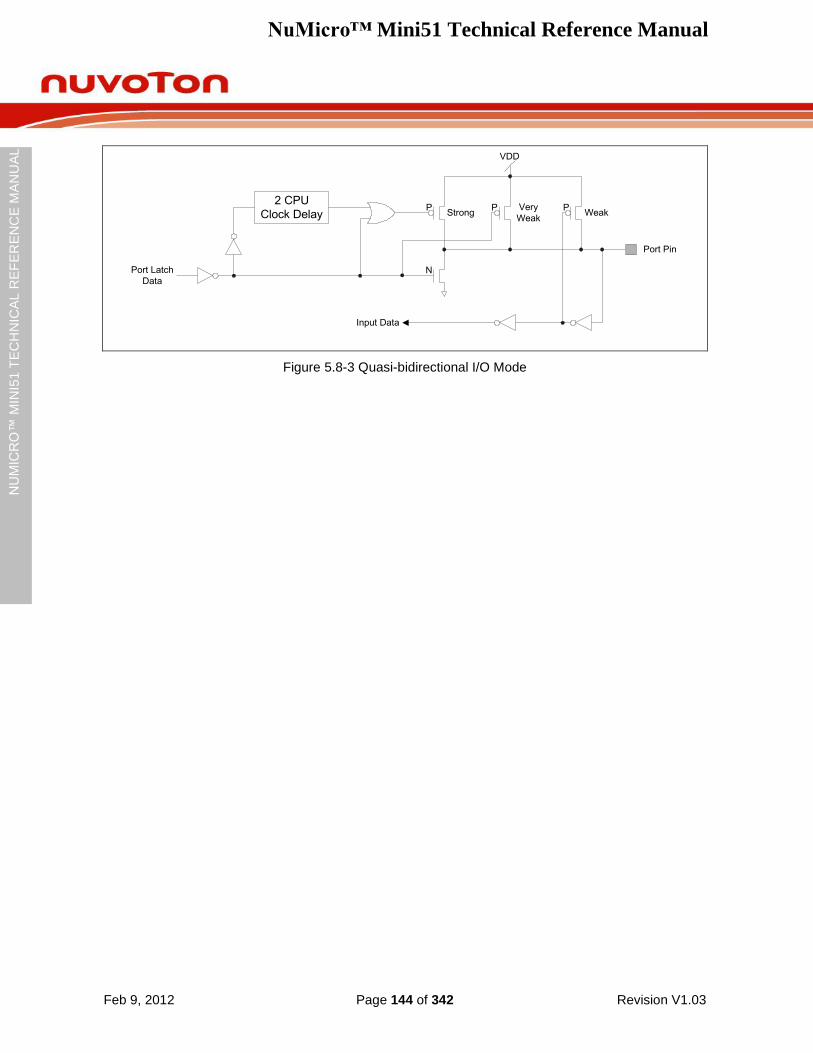
NuMicro™ Mini51 Technical Reference Manual
Feb 9, 2012 Page 144 of 342 Revision V1.03
NU
MIC
RO
™ M
INI5
1 T
EC
HN
ICA
L R
EF
ER
EN
CE
MA
NU
AL
Port Pin
2 CPU
Clock Delay
Input Data
Port Latch
Data
P P P
N
VDD
StrongVery
WeakWeak
Figure 5.8-3 Quasi-bidirectional I/O Mode
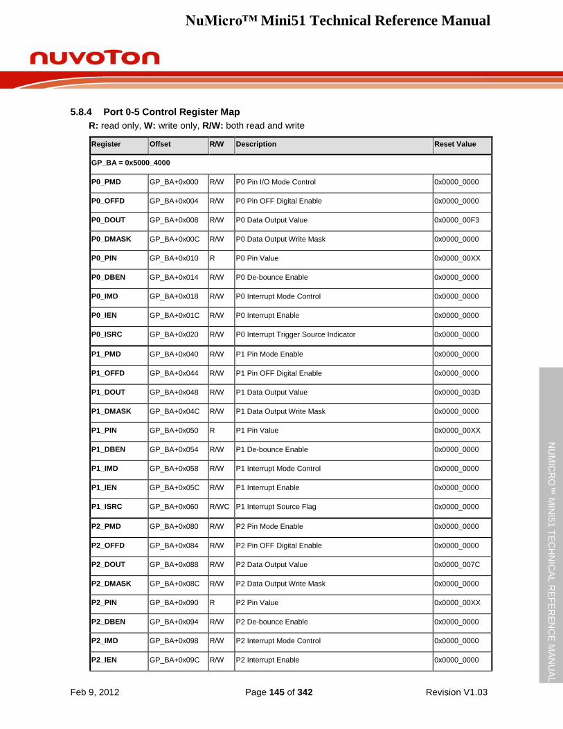
NuMicro™ Mini51 Technical Reference Manual
Feb 9, 2012 Page 145 of 342 Revision V1.03
NU
MIC
RO
™ M
INI5
1 T
EC
HN
ICA
L R
EF
ER
EN
CE
MA
NU
AL
5.8.4 Port 0-5 Control Register Map
R: read only, W: write only, R/W: both read and write
Register Offset R/W Description Reset Value
GP_BA = 0x5000_4000
P0_PMD GP_BA+0x000 R/W P0 Pin I/O Mode Control 0x0000_0000
P0_OFFD GP_BA+0x004 R/W P0 Pin OFF Digital Enable 0x0000_0000
P0_DOUT GP_BA+0x008 R/W P0 Data Output Value 0x0000_00F3
P0_DMASK GP_BA+0x00C R/W P0 Data Output Write Mask 0x0000_0000
P0_PIN GP_BA+0x010 R P0 Pin Value 0x0000_00XX
P0_DBEN GP_BA+0x014 R/W P0 De-bounce Enable 0x0000_0000
P0_IMD GP_BA+0x018 R/W P0 Interrupt Mode Control 0x0000_0000
P0_IEN GP_BA+0x01C R/W P0 Interrupt Enable 0x0000_0000
P0_ISRC GP_BA+0x020 R/W P0 Interrupt Trigger Source Indicator 0x0000_0000
P1_PMD GP_BA+0x040 R/W P1 Pin Mode Enable 0x0000_0000
P1_OFFD GP_BA+0x044 R/W P1 Pin OFF Digital Enable 0x0000_0000
P1_DOUT GP_BA+0x048 R/W P1 Data Output Value 0x0000_003D
P1_DMASK GP_BA+0x04C R/W P1 Data Output Write Mask 0x0000_0000
P1_PIN GP_BA+0x050 R P1 Pin Value 0x0000_00XX
P1_DBEN GP_BA+0x054 R/W P1 De-bounce Enable 0x0000_0000
P1_IMD GP_BA+0x058 R/W P1 Interrupt Mode Control 0x0000_0000
P1_IEN GP_BA+0x05C R/W P1 Interrupt Enable 0x0000_0000
P1_ISRC GP_BA+0x060 R/WC P1 Interrupt Source Flag 0x0000_0000
P2_PMD GP_BA+0x080 R/W P2 Pin Mode Enable 0x0000_0000
P2_OFFD GP_BA+0x084 R/W P2 Pin OFF Digital Enable 0x0000_0000
P2_DOUT GP_BA+0x088 R/W P2 Data Output Value 0x0000_007C
P2_DMASK GP_BA+0x08C R/W P2 Data Output Write Mask 0x0000_0000
P2_PIN GP_BA+0x090 R P2 Pin Value 0x0000_00XX
P2_DBEN GP_BA+0x094 R/W P2 De-bounce Enable 0x0000_0000
P2_IMD GP_BA+0x098 R/W P2 Interrupt Mode Control 0x0000_0000
P2_IEN GP_BA+0x09C R/W P2 Interrupt Enable 0x0000_0000
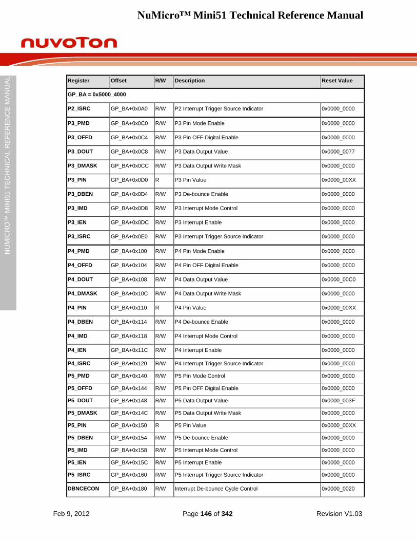
NuMicro™ Mini51 Technical Reference Manual
Feb 9, 2012 Page 146 of 342 Revision V1.03
NU
MIC
RO
™ M
INI5
1 T
EC
HN
ICA
L R
EF
ER
EN
CE
MA
NU
AL
Register Offset R/W Description Reset Value
GP_BA = 0x5000_4000
P2_ISRC GP_BA+0x0A0 R/W P2 Interrupt Trigger Source Indicator 0x0000_0000
P3_PMD GP_BA+0x0C0 R/W P3 Pin Mode Enable 0x0000_0000
P3_OFFD GP_BA+0x0C4 R/W P3 Pin OFF Digital Enable 0x0000_0000
P3_DOUT GP_BA+0x0C8 R/W P3 Data Output Value 0x0000_0077
P3_DMASK GP_BA+0x0CC R/W P3 Data Output Write Mask 0x0000_0000
P3_PIN GP_BA+0x0D0 R P3 Pin Value 0x0000_00XX
P3_DBEN GP_BA+0x0D4 R/W P3 De-bounce Enable 0x0000_0000
P3_IMD GP_BA+0x0D8 R/W P3 Interrupt Mode Control 0x0000_0000
P3_IEN GP_BA+0x0DC R/W P3 Interrupt Enable 0x0000_0000
P3_ISRC GP_BA+0x0E0 R/W P3 Interrupt Trigger Source Indicator 0x0000_0000
P4_PMD GP_BA+0x100 R/W P4 Pin Mode Enable 0x0000_0000
P4_OFFD GP_BA+0x104 R/W P4 Pin OFF Digital Enable 0x0000_0000
P4_DOUT GP_BA+0x108 R/W P4 Data Output Value 0x0000_00C0
P4_DMASK GP_BA+0x10C R/W P4 Data Output Write Mask 0x0000_0000
P4_PIN GP_BA+0x110 R P4 Pin Value 0x0000_00XX
P4_DBEN GP_BA+0x114 R/W P4 De-bounce Enable 0x0000_0000
P4_IMD GP_BA+0x118 R/W P4 Interrupt Mode Control 0x0000_0000
P4_IEN GP_BA+0x11C R/W P4 Interrupt Enable 0x0000_0000
P4_ISRC GP_BA+0x120 R/W P4 Interrupt Trigger Source Indicator 0x0000_0000
P5_PMD GP_BA+0x140 R/W P5 Pin Mode Control 0x0000_0000
P5_OFFD GP_BA+0x144 R/W P5 Pin OFF Digital Enable 0x0000_0000
P5_DOUT GP_BA+0x148 R/W P5 Data Output Value 0x0000_003F
P5_DMASK GP_BA+0x14C R/W P5 Data Output Write Mask 0x0000_0000
P5_PIN GP_BA+0x150 R P5 Pin Value 0x0000_00XX
P5_DBEN GP_BA+0x154 R/W P5 De-bounce Enable 0x0000_0000
P5_IMD GP_BA+0x158 R/W P5 Interrupt Mode Control 0x0000_0000
P5_IEN GP_BA+0x15C R/W P5 Interrupt Enable 0x0000_0000
P5_ISRC GP_BA+0x160 R/W P5 Interrupt Trigger Source Indicator 0x0000_0000
DBNCECON GP_BA+0x180 R/W Interrupt De-bounce Cycle Control 0x0000_0020
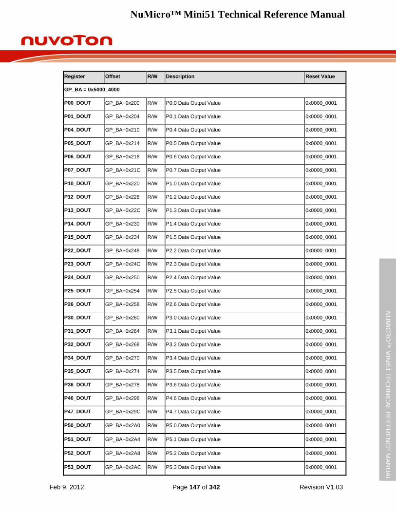
NuMicro™ Mini51 Technical Reference Manual
Feb 9, 2012 Page 147 of 342 Revision V1.03
NU
MIC
RO
™ M
INI5
1 T
EC
HN
ICA
L R
EF
ER
EN
CE
MA
NU
AL
Register Offset R/W Description Reset Value
GP_BA = 0x5000_4000
P00_DOUT GP_BA+0x200 R/W P0.0 Data Output Value 0x0000_0001
P01_DOUT GP_BA+0x204 R/W P0.1 Data Output Value 0x0000_0001
P04_DOUT GP_BA+0x210 R/W P0.4 Data Output Value 0x0000_0001
P05_DOUT GP_BA+0x214 R/W P0.5 Data Output Value 0x0000_0001
P06_DOUT GP_BA+0x218 R/W P0.6 Data Output Value 0x0000_0001
P07_DOUT GP_BA+0x21C R/W P0.7 Data Output Value 0x0000_0001
P10_DOUT GP_BA+0x220 R/W P1.0 Data Output Value 0x0000_0001
P12_DOUT GP_BA+0x228 R/W P1.2 Data Output Value 0x0000_0001
P13_DOUT GP_BA+0x22C R/W P1.3 Data Output Value 0x0000_0001
P14_DOUT GP_BA+0x230 R/W P1.4 Data Output Value 0x0000_0001
P15_DOUT GP_BA+0x234 R/W P1.5 Data Output Value 0x0000_0001
P22_DOUT GP_BA+0x248 R/W P2.2 Data Output Value 0x0000_0001
P23_DOUT GP_BA+0x24C R/W P2.3 Data Output Value 0x0000_0001
P24_DOUT GP_BA+0x250 R/W P2.4 Data Output Value 0x0000_0001
P25_DOUT GP_BA+0x254 R/W P2.5 Data Output Value 0x0000_0001
P26_DOUT GP_BA+0x258 R/W P2.6 Data Output Value 0x0000_0001
P30_DOUT GP_BA+0x260 R/W P3.0 Data Output Value 0x0000_0001
P31_DOUT GP_BA+0x264 R/W P3.1 Data Output Value 0x0000_0001
P32_DOUT GP_BA+0x268 R/W P3.2 Data Output Value 0x0000_0001
P34_DOUT GP_BA+0x270 R/W P3.4 Data Output Value 0x0000_0001
P35_DOUT GP_BA+0x274 R/W P3.5 Data Output Value 0x0000_0001
P36_DOUT GP_BA+0x278 R/W P3.6 Data Output Value 0x0000_0001
P46_DOUT GP_BA+0x298 R/W P4.6 Data Output Value 0x0000_0001
P47_DOUT GP_BA+0x29C R/W P4.7 Data Output Value 0x0000_0001
P50_DOUT GP_BA+0x2A0 R/W P5.0 Data Output Value 0x0000_0001
P51_DOUT GP_BA+0x2A4 R/W P5.1 Data Output Value 0x0000_0001
P52_DOUT GP_BA+0x2A8 R/W P5.2 Data Output Value 0x0000_0001
P53_DOUT GP_BA+0x2AC R/W P5.3 Data Output Value 0x0000_0001
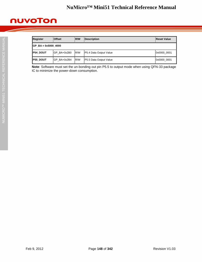
NuMicro™ Mini51 Technical Reference Manual
Feb 9, 2012 Page 148 of 342 Revision V1.03
NU
MIC
RO
™ M
INI5
1 T
EC
HN
ICA
L R
EF
ER
EN
CE
MA
NU
AL
Register Offset R/W Description Reset Value
GP_BA = 0x5000_4000
P54_DOUT GP_BA+0x2B0 R/W P5.4 Data Output Value 0x0000_0001
P55_DOUT GP_BA+0x2B4 R/W P5.5 Data Output Value 0x0000_0001
Note: Software must set the un-bonding out pin P5.5 to output mode when using QFN-33 package IC to minimize the power-down consumption.
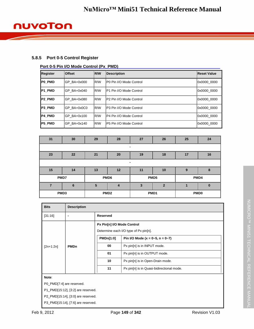
NuMicro™ Mini51 Technical Reference Manual
Feb 9, 2012 Page 149 of 342 Revision V1.03
NU
MIC
RO
™ M
INI5
1 T
EC
HN
ICA
L R
EF
ER
EN
CE
MA
NU
AL
5.8.5 Port 0-5 Control Register
Port 0-5 Pin I/O Mode Control (Px_PMD)
Register Offset R/W Description Reset Value
P0_PMD GP_BA+0x000 R/W P0 Pin I/O Mode Control 0x0000_0000
P1_PMD GP_BA+0x040 R/W P1 Pin I/O Mode Control 0x0000_0000
P2_PMD GP_BA+0x080 R/W P2 Pin I/O Mode Control 0x0000_0000
P3_PMD GP_BA+0x0C0 R/W P3 Pin I/O Mode Control 0x0000_0000
P4_PMD GP_BA+0x100 R/W P4 Pin I/O Mode Control 0x0000_0000
P5_PMD GP_BA+0x140 R/W P5 Pin I/O Mode Control 0x0000_0000
31 30 29 28 27 26 25 24
-
23 22 21 20 19 18 17 16
-
15 14 13 12 11 10 9 8
PMD7 PMD6 PMD5 PMD4
7 6 5 4 3 2 1 0
PMD3 PMD2 PMD1 PMD0
Bits Description
[31:16] - Reserved
[2n+1:2n] PMDn
Px Pin[n] I/O Mode Control
Determine each I/O type of Px pin[n].
PMDn[1:0] Pin I/O Mode (x = 0~5, n = 0~7)
00 Px pin[n] is in INPUT mode.
01 Px pin[n] is in OUTPUT mode.
10 Px pin[n] is in Open-Drain mode.
11 Px pin[n] is in Quasi-bidirectional mode.
Note:
P0_PMD[7:4] are reserved.
P1_PMD[15:12], [3:2] are reserved.
P2_PMD[15:14], [3:0] are reserved.
P3_PMD[15:14], [7:6] are reserved.
NuMicro™ Mini51 Technical Reference Manual
Feb 9, 2012 Page 150 of 342 Revision V1.03
NU
MIC
RO
™ M
INI5
1 T
EC
HN
ICA
L R
EF
ER
EN
CE
MA
NU
AL
Bits Description
P4_PMD[11:0] are reserved.
P5_PMD[15:12] are reserved.
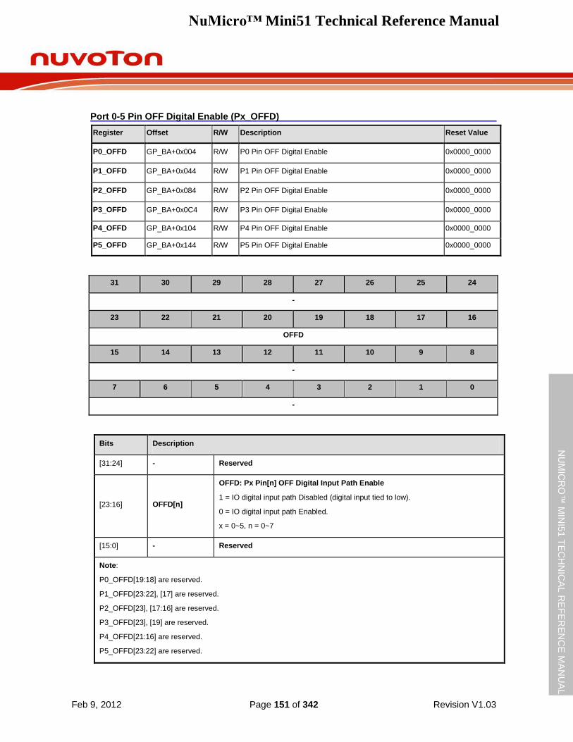
NuMicro™ Mini51 Technical Reference Manual
Feb 9, 2012 Page 151 of 342 Revision V1.03
NU
MIC
RO
™ M
INI5
1 T
EC
HN
ICA
L R
EF
ER
EN
CE
MA
NU
AL
Port 0-5 Pin OFF Digital Enable (Px_OFFD)
Register Offset R/W Description Reset Value
P0_OFFD GP_BA+0x004 R/W P0 Pin OFF Digital Enable 0x0000_0000
P1_OFFD GP_BA+0x044 R/W P1 Pin OFF Digital Enable 0x0000_0000
P2_OFFD GP_BA+0x084 R/W P2 Pin OFF Digital Enable 0x0000_0000
P3_OFFD GP_BA+0x0C4 R/W P3 Pin OFF Digital Enable 0x0000_0000
P4_OFFD GP_BA+0x104 R/W P4 Pin OFF Digital Enable 0x0000_0000
P5_OFFD GP_BA+0x144 R/W P5 Pin OFF Digital Enable 0x0000_0000
31 30 29 28 27 26 25 24
-
23 22 21 20 19 18 17 16
OFFD
15 14 13 12 11 10 9 8
-
7 6 5 4 3 2 1 0
-
Bits Description
[31:24] - Reserved
[23:16] OFFD[n]
OFFD: Px Pin[n] OFF Digital Input Path Enable
1 = IO digital input path Disabled (digital input tied to low).
0 = IO digital input path Enabled.
x = 0~5, n = 0~7
[15:0] - Reserved
Note:
P0_OFFD[19:18] are reserved.
P1_OFFD[23:22], [17] are reserved.
P2_OFFD[23], [17:16] are reserved.
P3_OFFD[23], [19] are reserved.
P4_OFFD[21:16] are reserved.
P5_OFFD[23:22] are reserved.
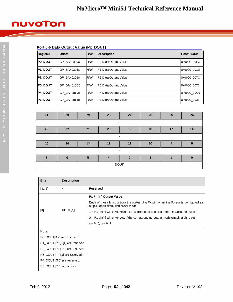
NuMicro™ Mini51 Technical Reference Manual
Feb 9, 2012 Page 152 of 342 Revision V1.03
NU
MIC
RO
™ M
INI5
1 T
EC
HN
ICA
L R
EF
ER
EN
CE
MA
NU
AL
Port 0-5 Data Output Value (Px_DOUT)
Register Offset R/W Description Reset Value
P0_DOUT GP_BA+0x008 R/W P0 Data Output Value 0x0000_00F3
P1_DOUT GP_BA+0x048 R/W P1 Data Output Value 0x0000_003D
P2_DOUT GP_BA+0x088 R/W P2 Data Output Value 0x0000_007C
P3_DOUT GP_BA+0x0C8 R/W P3 Data Output Value 0x0000_0077
P4_DOUT GP_BA+0x108 R/W P4 Data Output Value 0x0000_00C0
P5_DOUT GP_BA+0x148 R/W P5 Data Output Value 0x0000_003F
31 30 29 28 27 26 25 24
-
23 22 21 20 19 18 17 16
-
15 14 13 12 11 10 9 8
-
7 6 5 4 3 2 1 0
DOUT
Bits Description
[31:8] - Reserved
[n] DOUT[n]
Px Pin[n] Output Value
Each of these bits controls the status of a Px pin when the Px pin is configured as output, open-drain and quasi-mode.
1 = Px pin[n] will drive High if the corresponding output mode enabling bit is set.
0 = Px pin[n] will drive Low if the corresponding output mode enabling bit is set.
x = 0~5, n = 0~7
Note:
P0_DOUT[3:2] are reserved.
P1_DOUT [7:6], [1] are reserved.
P2_DOUT [7], [1:0] are reserved.
P3_DOUT [7], [3] are reserved.
P4_DOUT [5:0] are reserved.
P5_DOUT [7:6] are reserved.
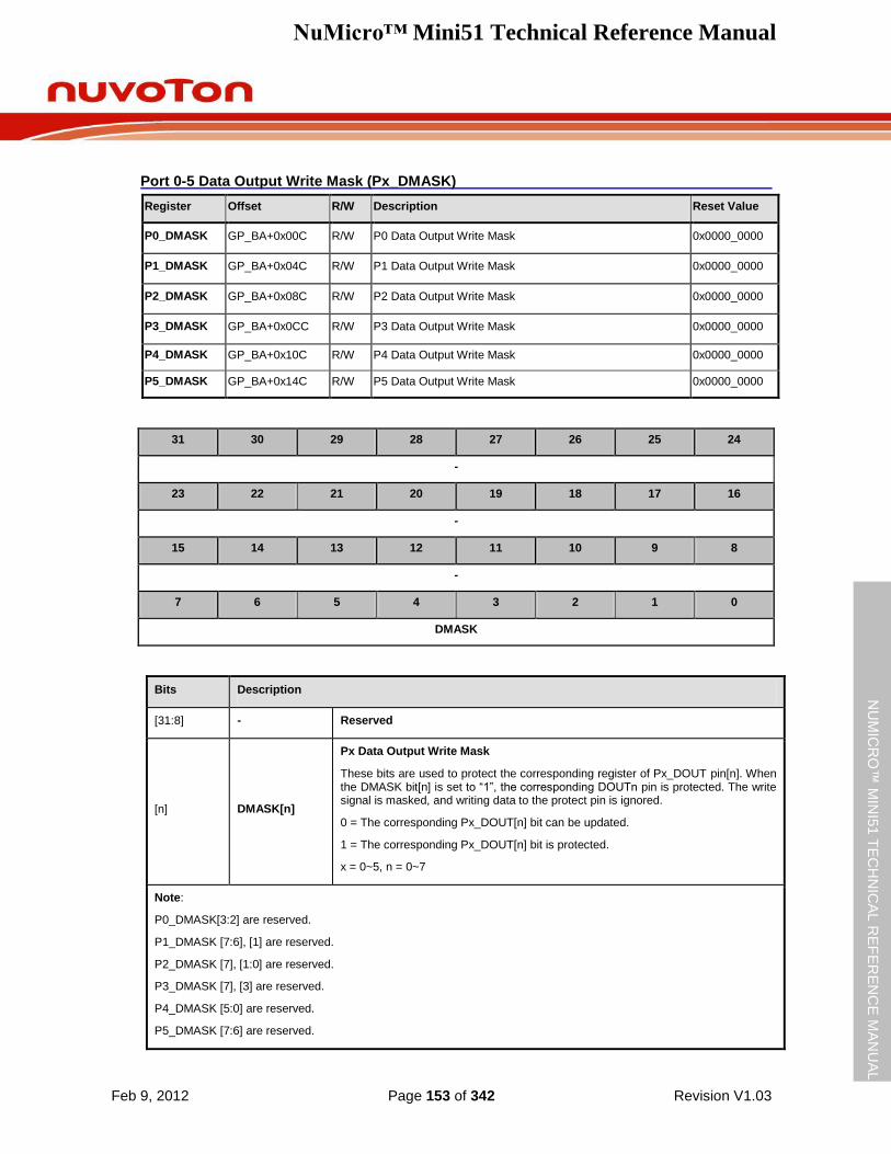
NuMicro™ Mini51 Technical Reference Manual
Feb 9, 2012 Page 153 of 342 Revision V1.03
NU
MIC
RO
™ M
INI5
1 T
EC
HN
ICA
L R
EF
ER
EN
CE
MA
NU
AL
Port 0-5 Data Output Write Mask (Px_DMASK)
Register Offset R/W Description Reset Value
P0_DMASK GP_BA+0x00C R/W P0 Data Output Write Mask 0x0000_0000
P1_DMASK GP_BA+0x04C R/W P1 Data Output Write Mask 0x0000_0000
P2_DMASK GP_BA+0x08C R/W P2 Data Output Write Mask 0x0000_0000
P3_DMASK GP_BA+0x0CC R/W P3 Data Output Write Mask 0x0000_0000
P4_DMASK GP_BA+0x10C R/W P4 Data Output Write Mask 0x0000_0000
P5_DMASK GP_BA+0x14C R/W P5 Data Output Write Mask 0x0000_0000
31 30 29 28 27 26 25 24
-
23 22 21 20 19 18 17 16
-
15 14 13 12 11 10 9 8
-
7 6 5 4 3 2 1 0
DMASK
Bits Description
[31:8] - Reserved
[n] DMASK[n]
Px Data Output Write Mask
These bits are used to protect the corresponding register of Px_DOUT pin[n]. When the DMASK bit[n] is set to “1”, the corresponding DOUTn pin is protected. The write signal is masked, and writing data to the protect pin is ignored.
0 = The corresponding Px_DOUT[n] bit can be updated.
1 = The corresponding Px_DOUT[n] bit is protected.
x = 0~5, n = 0~7
Note:
P0_DMASK[3:2] are reserved.
P1_DMASK [7:6], [1] are reserved.
P2_DMASK [7], [1:0] are reserved.
P3_DMASK [7], [3] are reserved.
P4_DMASK [5:0] are reserved.
P5_DMASK [7:6] are reserved.
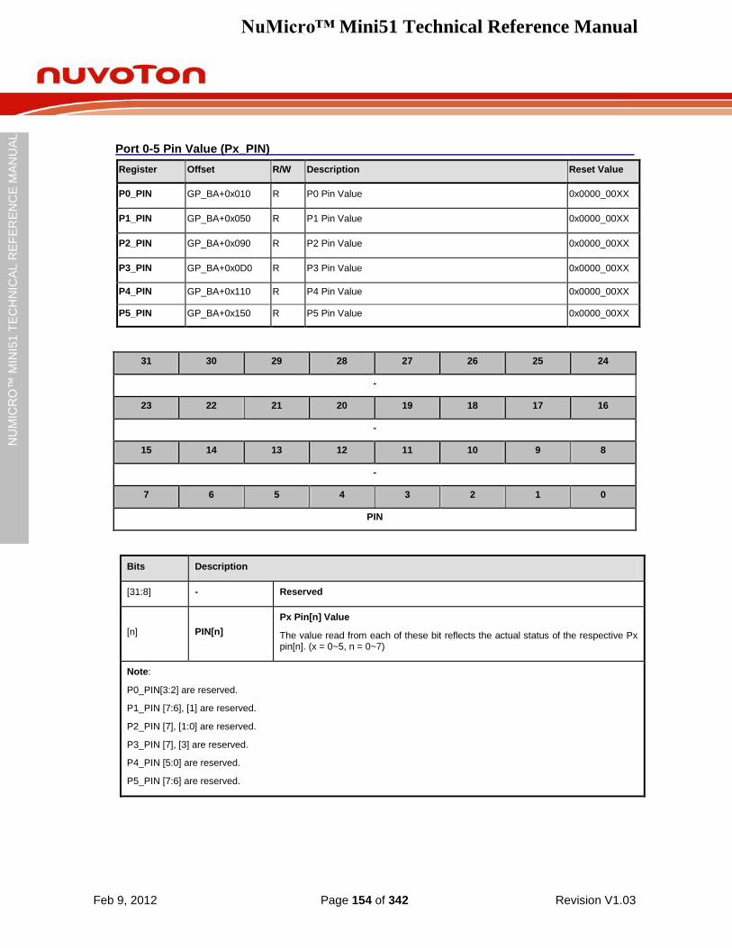
NuMicro™ Mini51 Technical Reference Manual
Feb 9, 2012 Page 154 of 342 Revision V1.03
NU
MIC
RO
™ M
INI5
1 T
EC
HN
ICA
L R
EF
ER
EN
CE
MA
NU
AL
Port 0-5 Pin Value (Px_PIN)
Register Offset R/W Description Reset Value
P0_PIN GP_BA+0x010 R P0 Pin Value 0x0000_00XX
P1_PIN GP_BA+0x050 R P1 Pin Value 0x0000_00XX
P2_PIN GP_BA+0x090 R P2 Pin Value 0x0000_00XX
P3_PIN GP_BA+0x0D0 R P3 Pin Value 0x0000_00XX
P4_PIN GP_BA+0x110 R P4 Pin Value 0x0000_00XX
P5_PIN GP_BA+0x150 R P5 Pin Value 0x0000_00XX
31 30 29 28 27 26 25 24
-
23 22 21 20 19 18 17 16
-
15 14 13 12 11 10 9 8
-
7 6 5 4 3 2 1 0
PIN
Bits Description
[31:8] - Reserved
[n] PIN[n]
Px Pin[n] Value
The value read from each of these bit reflects the actual status of the respective Px pin[n]. (x = 0~5, n = 0~7)
Note:
P0_PIN[3:2] are reserved.
P1_PIN [7:6], [1] are reserved.
P2_PIN [7], [1:0] are reserved.
P3_PIN [7], [3] are reserved.
P4_PIN [5:0] are reserved.
P5_PIN [7:6] are reserved.

NuMicro™ Mini51 Technical Reference Manual
Feb 9, 2012 Page 155 of 342 Revision V1.03
NU
MIC
RO
™ M
INI5
1 T
EC
HN
ICA
L R
EF
ER
EN
CE
MA
NU
AL
Port 0-5 De-bounce Enable (Px_DBEN)
Register Offset R/W Description Reset Value
P0_DBEN GP_BA+0x014 R/W P0 De-bounce Enable 0x0000_0000
P1_DBEN GP_BA+0x054 R/W P1 De-bounce Enable 0x0000_0000
P2_DBEN GP_BA+0x094 R/W P2 De-bounce Enable 0x0000_0000
P3_DBEN GP_BA+0x0D4 R/W P3 De-bounce Enable 0x0000_0000
P4_DBEN GP_BA+0x114 R/W P4 De-bounce Enable 0x0000_0000
P5_DBEN GP_BA+0x154 R/W P5 De-bounce Enable 0x0000_0000
31 30 29 28 27 26 25 24
-
23 22 21 20 19 18 17 16
-
15 14 13 12 11 10 9 8
-
7 6 5 4 3 2 1 0
DBEN
Bits Description
[31:8] - Reserved
[n] DBEN[n]
Px Input Signal De-bounce Enable
DBEN[n] is used to enable the de-bounce function for each corresponding bit. If the input signal pulse width can‟t be sampled by continuous two de-bounce sample cycle, the input signal transition is regarded as the signal bounce and will not trigger the interrupt.
The DBEN[n] is used for “edge-trigger” interrupt only, and is ignored for “level trigger” interrupt.
0 = The pin[n] de-bounce function disabled.
1 = The pin[n] de-bounce function enabled.
The de-bounce function is valid for edge triggered interrupt. If the interrupt mode is level triggered, the de-bounce enable bit is ignored.
x = 0~5, n = 0~7

NuMicro™ Mini51 Technical Reference Manual
Feb 9, 2012 Page 156 of 342 Revision V1.03
NU
MIC
RO
™ M
INI5
1 T
EC
HN
ICA
L R
EF
ER
EN
CE
MA
NU
AL
Bits Description
Note:
P0_DBEN[3:2] are reserved.
P1_DBEN [7:6], [1] are reserved.
P2_DBEN [7], [1:0] are reserved.
P3_DBEN [7], [3] are reserved.
P4_DBEN [5:0] are reserved.
P5_DBEN [7:6] are reserved.

NuMicro™ Mini51 Technical Reference Manual
Feb 9, 2012 Page 157 of 342 Revision V1.03
NU
MIC
RO
™ M
INI5
1 T
EC
HN
ICA
L R
EF
ER
EN
CE
MA
NU
AL
Port 0-5 Interrupt Mode Control (Px_IMD)
Register Offset R/W Description Reset Value
P0_IMD GP_BA+0x018 R/W P0 Interrupt Mode Control 0x0000_0000
P1_IMD GP_BA+0x058 R/W P1 Interrupt Mode Control 0x0000_0000
P2_IMD GP_BA+0x098 R/W P2 Interrupt Mode Control 0x0000_0000
P3_IMD GP_BA+0x0D8 R/W P3 Interrupt Mode Control 0x0000_0000
P4_IMD GP_BA+0x118 R/W P4 Interrupt Mode Control 0x0000_0000
P5_IMD GP_BA+0x158 R/W P5 Interrupt Mode Control 0x0000_0000
31 30 29 28 27 26 25 24
-
23 22 21 20 19 18 17 16
-
15 14 13 12 11 10 9 8
-
7 6 5 4 3 2 1 0
IMD
Bits Description
[31:8] - Reserved
[n] IMD[n]
Port 0-5 Interrupt Mode Control
IMD[n] is used to control the interrupt by level trigger or edge trigger. If the interrupt is by edge trigger, the trigger source is control de-bounced. If the interrupt is by level trigger, the input source is sampled by one clock and then generates the interrupt.
0 = Edge trigger interrupt.
1 = Level trigger interrupt.
If pin is set as the level trigger interrupt, then only one level can be set on the registers Px_IEN. If both the level is set to trigger interrupt, the setting is ignored and no interrupt will occur.
The de-bounce function is valid for edge triggered interrupt. If the interrupt mode is level triggered, the de-bounce enable bit is ignored.
x = 0~5, n = 0~7
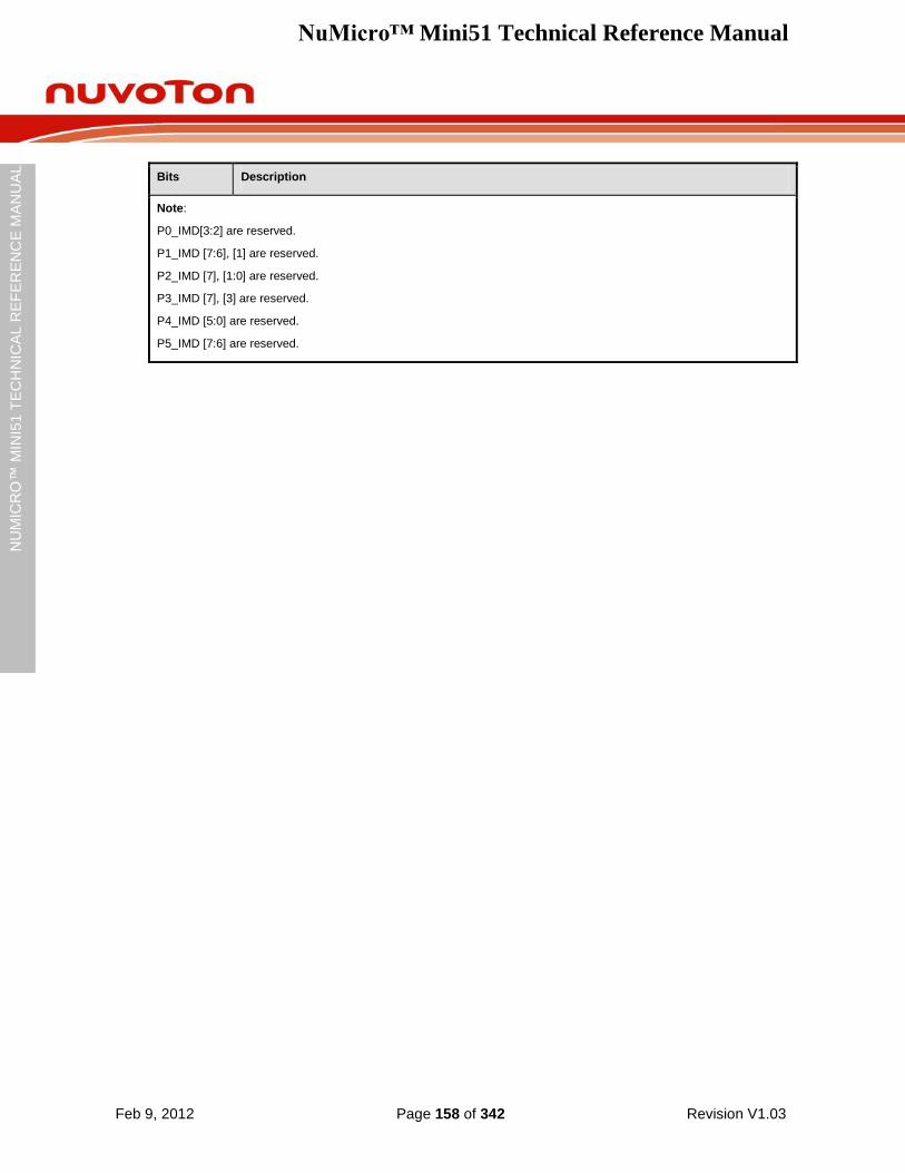
NuMicro™ Mini51 Technical Reference Manual
Feb 9, 2012 Page 158 of 342 Revision V1.03
NU
MIC
RO
™ M
INI5
1 T
EC
HN
ICA
L R
EF
ER
EN
CE
MA
NU
AL
Bits Description
Note:
P0_IMD[3:2] are reserved.
P1_IMD [7:6], [1] are reserved.
P2_IMD [7], [1:0] are reserved.
P3_IMD [7], [3] are reserved.
P4_IMD [5:0] are reserved.
P5_IMD [7:6] are reserved.
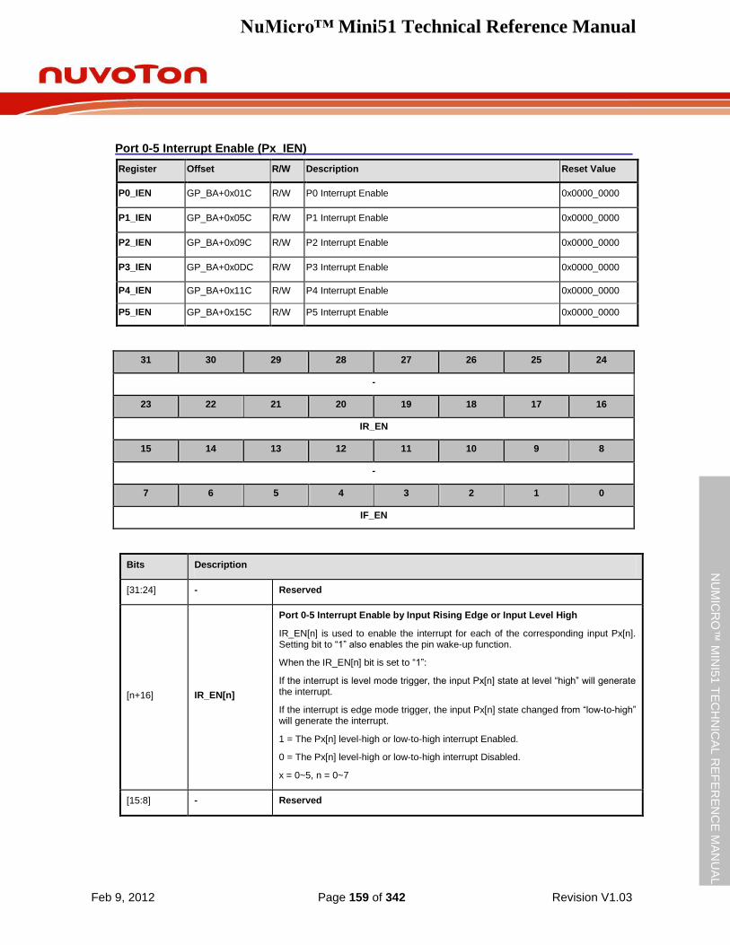
NuMicro™ Mini51 Technical Reference Manual
Feb 9, 2012 Page 159 of 342 Revision V1.03
NU
MIC
RO
™ M
INI5
1 T
EC
HN
ICA
L R
EF
ER
EN
CE
MA
NU
AL
Port 0-5 Interrupt Enable (Px_IEN)
Register Offset R/W Description Reset Value
P0_IEN GP_BA+0x01C R/W P0 Interrupt Enable 0x0000_0000
P1_IEN GP_BA+0x05C R/W P1 Interrupt Enable 0x0000_0000
P2_IEN GP_BA+0x09C R/W P2 Interrupt Enable 0x0000_0000
P3_IEN GP_BA+0x0DC R/W P3 Interrupt Enable 0x0000_0000
P4_IEN GP_BA+0x11C R/W P4 Interrupt Enable 0x0000_0000
P5_IEN GP_BA+0x15C R/W P5 Interrupt Enable 0x0000_0000
31 30 29 28 27 26 25 24
-
23 22 21 20 19 18 17 16
IR_EN
15 14 13 12 11 10 9 8
-
7 6 5 4 3 2 1 0
IF_EN
Bits Description
[31:24] - Reserved
[n+16] IR_EN[n]
Port 0-5 Interrupt Enable by Input Rising Edge or Input Level High
IR_EN[n] is used to enable the interrupt for each of the corresponding input Px[n]. Setting bit to “1” also enables the pin wake-up function.
When the IR_EN[n] bit is set to “1”:
If the interrupt is level mode trigger, the input Px[n] state at level “high” will generate the interrupt.
If the interrupt is edge mode trigger, the input Px[n] state changed from “low-to-high” will generate the interrupt.
1 = The Px[n] level-high or low-to-high interrupt Enabled.
0 = The Px[n] level-high or low-to-high interrupt Disabled.
x = 0~5, n = 0~7
[15:8] - Reserved
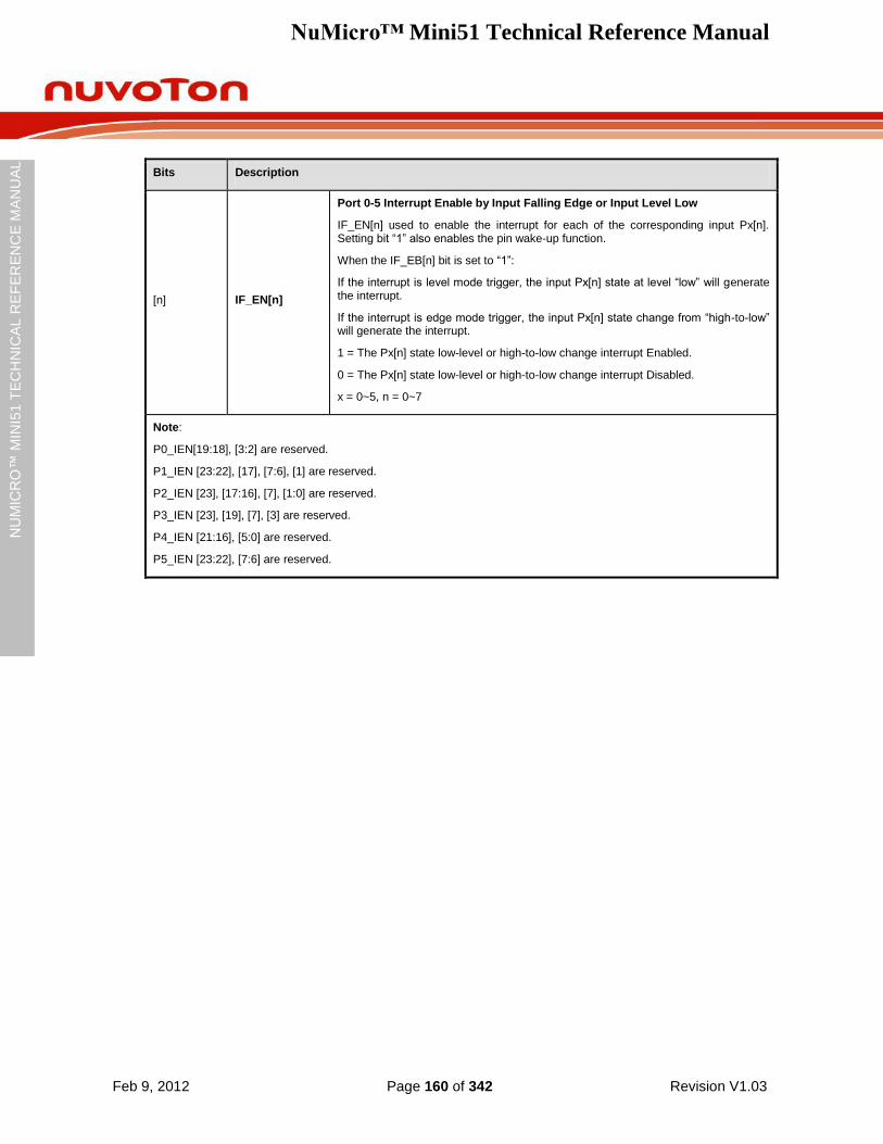
NuMicro™ Mini51 Technical Reference Manual
Feb 9, 2012 Page 160 of 342 Revision V1.03
NU
MIC
RO
™ M
INI5
1 T
EC
HN
ICA
L R
EF
ER
EN
CE
MA
NU
AL
Bits Description
[n] IF_EN[n]
Port 0-5 Interrupt Enable by Input Falling Edge or Input Level Low
IF_EN[n] used to enable the interrupt for each of the corresponding input Px[n]. Setting bit “1” also enables the pin wake-up function.
When the IF_EB[n] bit is set to “1”:
If the interrupt is level mode trigger, the input Px[n] state at level “low” will generate the interrupt.
If the interrupt is edge mode trigger, the input Px[n] state change from “high-to-low” will generate the interrupt.
1 = The Px[n] state low-level or high-to-low change interrupt Enabled.
0 = The Px[n] state low-level or high-to-low change interrupt Disabled.
x = 0~5, n = 0~7
Note:
P0_IEN[19:18], [3:2] are reserved.
P1_IEN [23:22], [17], [7:6], [1] are reserved.
P2_IEN [23], [17:16], [7], [1:0] are reserved.
P3_IEN [23], [19], [7], [3] are reserved.
P4_IEN [21:16], [5:0] are reserved.
P5_IEN [23:22], [7:6] are reserved.
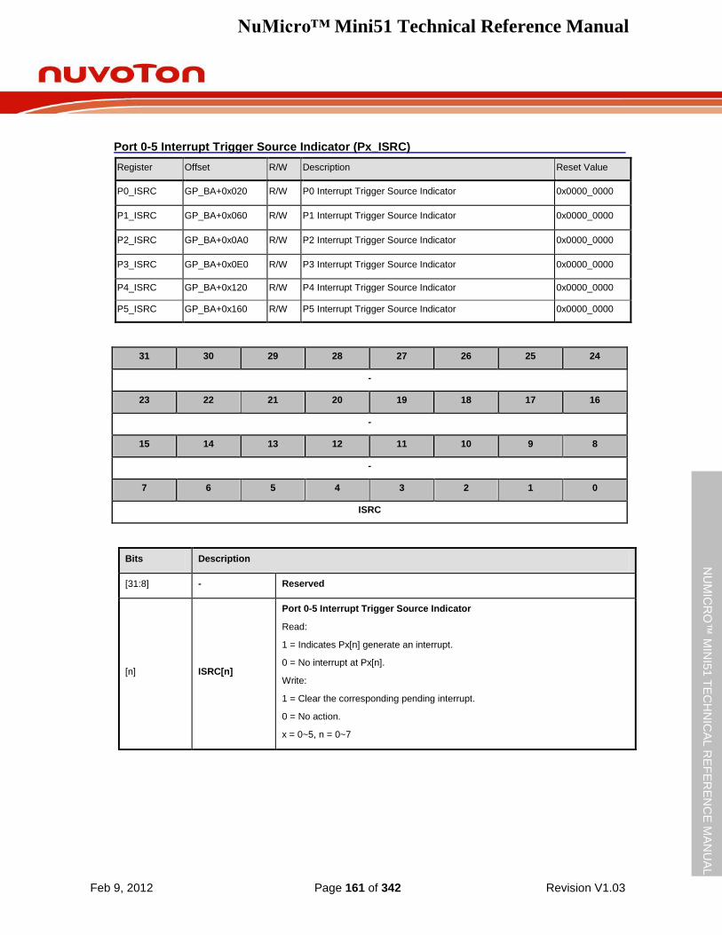
NuMicro™ Mini51 Technical Reference Manual
Feb 9, 2012 Page 161 of 342 Revision V1.03
NU
MIC
RO
™ M
INI5
1 T
EC
HN
ICA
L R
EF
ER
EN
CE
MA
NU
AL
Port 0-5 Interrupt Trigger Source Indicator (Px_ISRC)
Register Offset R/W Description Reset Value
P0_ISRC GP_BA+0x020 R/W P0 Interrupt Trigger Source Indicator 0x0000_0000
P1_ISRC GP_BA+0x060 R/W P1 Interrupt Trigger Source Indicator 0x0000_0000
P2_ISRC GP_BA+0x0A0 R/W P2 Interrupt Trigger Source Indicator 0x0000_0000
P3_ISRC GP_BA+0x0E0 R/W P3 Interrupt Trigger Source Indicator 0x0000_0000
P4_ISRC GP_BA+0x120 R/W P4 Interrupt Trigger Source Indicator 0x0000_0000
P5_ISRC GP_BA+0x160 R/W P5 Interrupt Trigger Source Indicator 0x0000_0000
31 30 29 28 27 26 25 24
-
23 22 21 20 19 18 17 16
-
15 14 13 12 11 10 9 8
-
7 6 5 4 3 2 1 0
ISRC
Bits Description
[31:8] - Reserved
[n] ISRC[n]
Port 0-5 Interrupt Trigger Source Indicator
Read:
1 = Indicates Px[n] generate an interrupt.
0 = No interrupt at Px[n].
Write:
1 = Clear the corresponding pending interrupt.
0 = No action.
x = 0~5, n = 0~7

NuMicro™ Mini51 Technical Reference Manual
Feb 9, 2012 Page 162 of 342 Revision V1.03
NU
MIC
RO
™ M
INI5
1 T
EC
HN
ICA
L R
EF
ER
EN
CE
MA
NU
AL
Bits Description
Note:
P0_ISRC [3:2] are reserved.
P1_ISRC [7:6], [1] are reserved.
P2_ISRC [7], [1:0] are reserved.
P3_ISRC [7], [3] are reserved.
P4_ISRC [5:0] are reserved.
P5_ISRC [7:6] are reserved.
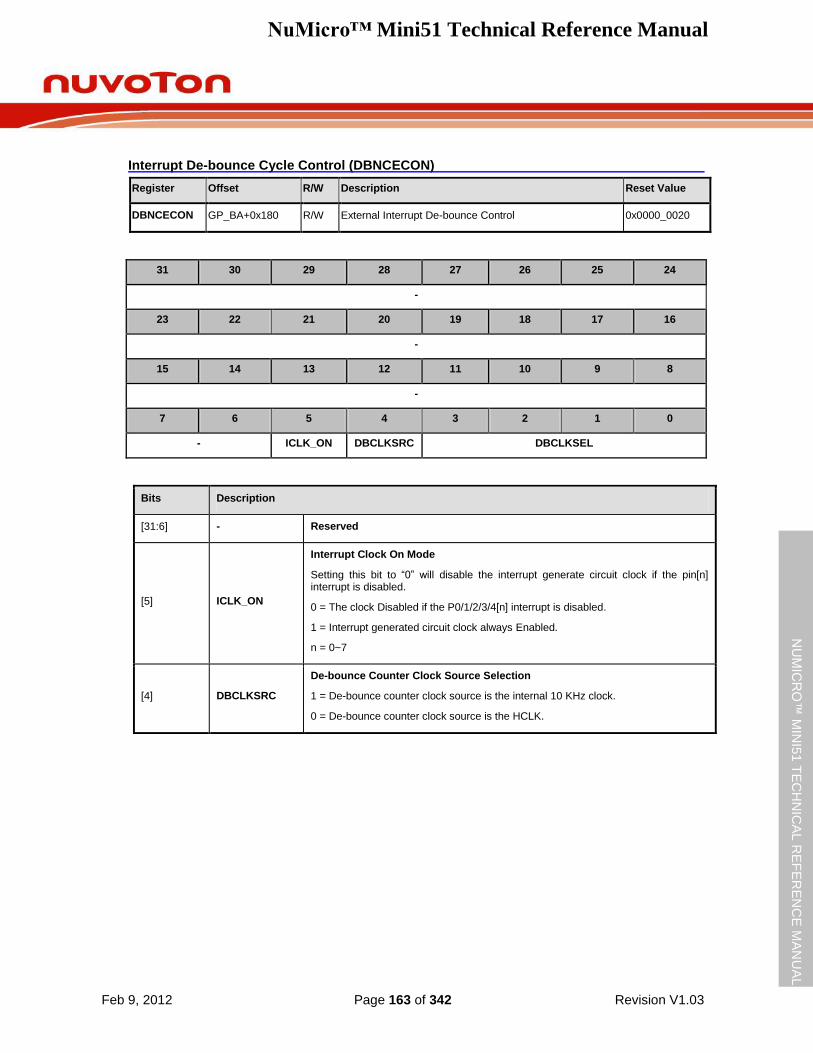
NuMicro™ Mini51 Technical Reference Manual
Feb 9, 2012 Page 163 of 342 Revision V1.03
NU
MIC
RO
™ M
INI5
1 T
EC
HN
ICA
L R
EF
ER
EN
CE
MA
NU
AL
Interrupt De-bounce Cycle Control (DBNCECON)
Register Offset R/W Description Reset Value
DBNCECON GP_BA+0x180 R/W External Interrupt De-bounce Control 0x0000_0020
31 30 29 28 27 26 25 24
-
23 22 21 20 19 18 17 16
-
15 14 13 12 11 10 9 8
-
7 6 5 4 3 2 1 0
- ICLK_ON DBCLKSRC DBCLKSEL
Bits Description
[31:6] - Reserved
[5] ICLK_ON
Interrupt Clock On Mode
Setting this bit to “0” will disable the interrupt generate circuit clock if the pin[n] interrupt is disabled.
0 = The clock Disabled if the P0/1/2/3/4[n] interrupt is disabled.
1 = Interrupt generated circuit clock always Enabled.
n = 0~7
[4] DBCLKSRC
De-bounce Counter Clock Source Selection
1 = De-bounce counter clock source is the internal 10 KHz clock.
0 = De-bounce counter clock source is the HCLK.
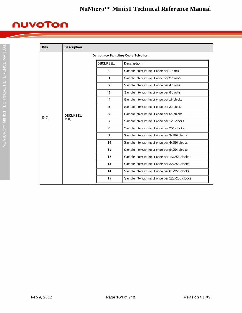
NuMicro™ Mini51 Technical Reference Manual
Feb 9, 2012 Page 164 of 342 Revision V1.03
NU
MIC
RO
™ M
INI5
1 T
EC
HN
ICA
L R
EF
ER
EN
CE
MA
NU
AL
Bits Description
[3:0] DBCLKSEL [3:0]
De-bounce Sampling Cycle Selection
DBCLKSEL Description
0 Sample interrupt input once per 1 clock
1 Sample interrupt input once per 2 clocks
2 Sample interrupt input once per 4 clocks
3 Sample interrupt input once per 8 clocks
4 Sample interrupt input once per 16 clocks
5 Sample interrupt input once per 32 clocks
6 Sample interrupt input once per 64 clocks
7 Sample interrupt input once per 128 clocks
8 Sample interrupt input once per 256 clocks
9 Sample interrupt input once per 2x256 clocks
10 Sample interrupt input once per 4x256 clocks
11 Sample interrupt input once per 8x256 clocks
12 Sample interrupt input once per 16x256 clocks
13 Sample interrupt input once per 32x256 clocks
14 Sample interrupt input once per 64x256 clocks
15 Sample interrupt input once per 128x256 clocks
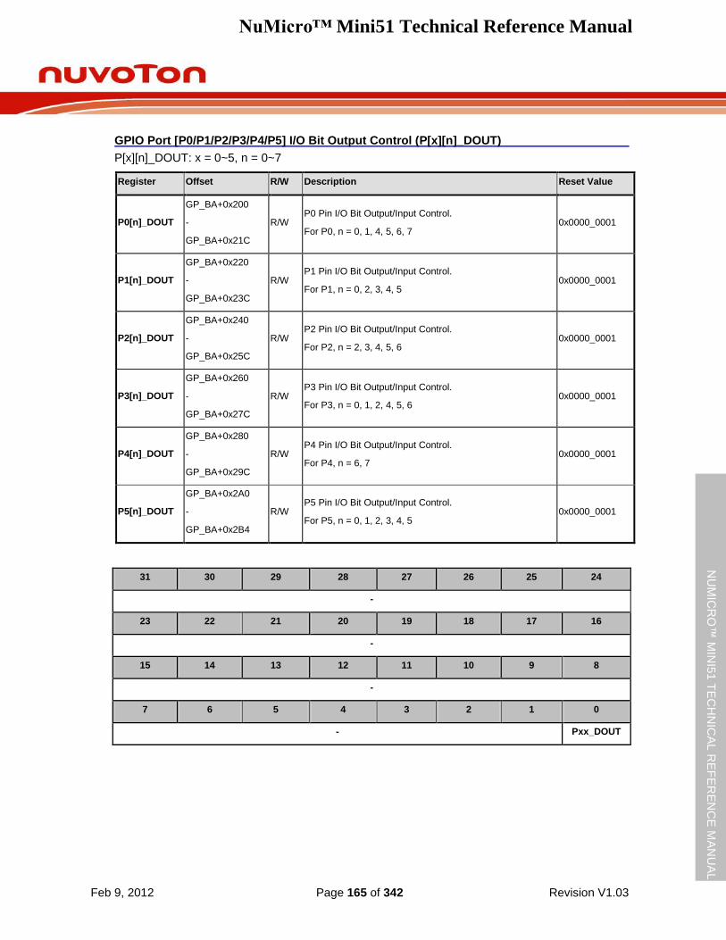
NuMicro™ Mini51 Technical Reference Manual
Feb 9, 2012 Page 165 of 342 Revision V1.03
NU
MIC
RO
™ M
INI5
1 T
EC
HN
ICA
L R
EF
ER
EN
CE
MA
NU
AL
GPIO Port [P0/P1/P2/P3/P4/P5] I/O Bit Output Control (P[x][n]_DOUT)
P[x][n]_DOUT: x = 0~5, n = 0~7
Register Offset R/W Description Reset Value
P0[n]_DOUT
GP_BA+0x200
-
GP_BA+0x21C
R/W P0 Pin I/O Bit Output/Input Control.
For P0, n = 0, 1, 4, 5, 6, 7 0x0000_0001
P1[n]_DOUT
GP_BA+0x220
-
GP_BA+0x23C
R/W P1 Pin I/O Bit Output/Input Control.
For P1, n = 0, 2, 3, 4, 5 0x0000_0001
P2[n]_DOUT
GP_BA+0x240
-
GP_BA+0x25C
R/W P2 Pin I/O Bit Output/Input Control.
For P2, n = 2, 3, 4, 5, 6 0x0000_0001
P3[n]_DOUT
GP_BA+0x260
-
GP_BA+0x27C
R/W P3 Pin I/O Bit Output/Input Control.
For P3, n = 0, 1, 2, 4, 5, 6 0x0000_0001
P4[n]_DOUT
GP_BA+0x280
-
GP_BA+0x29C
R/W P4 Pin I/O Bit Output/Input Control.
For P4, n = 6, 7 0x0000_0001
P5[n]_DOUT
GP_BA+0x2A0
-
GP_BA+0x2B4
R/W P5 Pin I/O Bit Output/Input Control.
For P5, n = 0, 1, 2, 3, 4, 5 0x0000_0001
31 30 29 28 27 26 25 24
-
23 22 21 20 19 18 17 16
-
15 14 13 12 11 10 9 8
-
7 6 5 4 3 2 1 0
- Pxx_DOUT
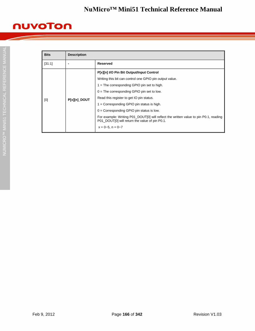
NuMicro™ Mini51 Technical Reference Manual
Feb 9, 2012 Page 166 of 342 Revision V1.03
NU
MIC
RO
™ M
INI5
1 T
EC
HN
ICA
L R
EF
ER
EN
CE
MA
NU
AL
Bits Description
[31:1] - Reserved
[0] P[x][n]_DOUT
P[x][n] I/O Pin Bit Output/Input Control
Writing this bit can control one GPIO pin output value.
1 = The corresponding GPIO pin set to high.
0 = The corresponding GPIO pin set to low.
Read this register to get IO pin status.
1 = Corresponding GPIO pin status is high.
0 = Corresponding GPIO pin status is low.
For example: Writing P01_DOUT[0] will reflect the written value to pin P0.1, reading P01_DOUT[0] will return the value of pin P0.1.
x = 0~5, n = 0~7
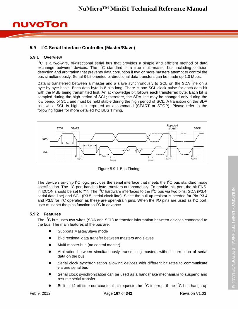
NuMicro™ Mini51 Technical Reference Manual
Feb 9, 2012 Page 167 of 342 Revision V1.03
NU
MIC
RO
™ M
INI5
1 T
EC
HN
ICA
L R
EF
ER
EN
CE
MA
NU
AL
5.9 I2C Serial Interface Controller (Master/Slave)
5.9.1 Overview
I2C is a two-wire, bi-directional serial bus that provides a simple and efficient method of data
exchange between devices. The I2C standard is a true multi-master bus including collision
detection and arbitration that prevents data corruption if two or more masters attempt to control the bus simultaneously. Serial 8-bit oriented bi-directional data transfers can be made up 1.0 Mbps.
Data is transferred between a master and a slave synchronously to SCL on the SDA line on a byte-by-byte basis. Each data byte is 8 bits long. There is one SCL clock pulse for each data bit with the MSB being transmitted first. An acknowledge bit follows each transferred byte. Each bit is sampled during the high period of SCL; therefore, the SDA line may be changed only during the low period of SCL and must be held stable during the high period of SCL. A transition on the SDA line while SCL is high is interpreted as a command (START or STOP). Please refer to the following figure for more detailed I
2C BUS Timing.
tBUF
STOP
SDA
SCL
START
tHD;STA
tLOW
tHD;DAT
tHIGH
tf
tSU;DAT
Repeated
START
tSU;STA tSU;STO
STOP
tr
Figure 5.9-1 Bus Timing
The device‟s on-chip I2C logic provides the serial interface that meets the I
2C bus standard mode
specification. The I2C port handles byte transfers autonomously. To enable this port, the bit ENSI
in I2CON should be set to “1”. The I2C hardware interfaces to the I
2C bus via two pins: SDA (P3.4,
serial data line) and SCL (P3.5, serial clock line). Since the pull-up resistor is needed for Pin P3.4 and P3.5 for I
2C operation as these are open-drain pins. When the I/O pins are used as I
2C port,
user must set the pins function to I2C in advance.
5.9.2 Features
The I2C bus uses two wires (SDA and SCL) to transfer information between devices connected to
the bus. The main features of the bus are:
Supports Master/Slave mode
Bi-directional data transfer between masters and slaves
Multi-master bus (no central master)
Arbitration between simultaneously transmitting masters without corruption of serial data on the bus
Serial clock synchronization allowing devices with different bit rates to communicate via one serial bus
Serial clock synchronization can be used as a handshake mechanism to suspend and resume serial transfer
Built-in 14-bit time-out counter that requests the I2C interrupt if the I
2C bus hangs up
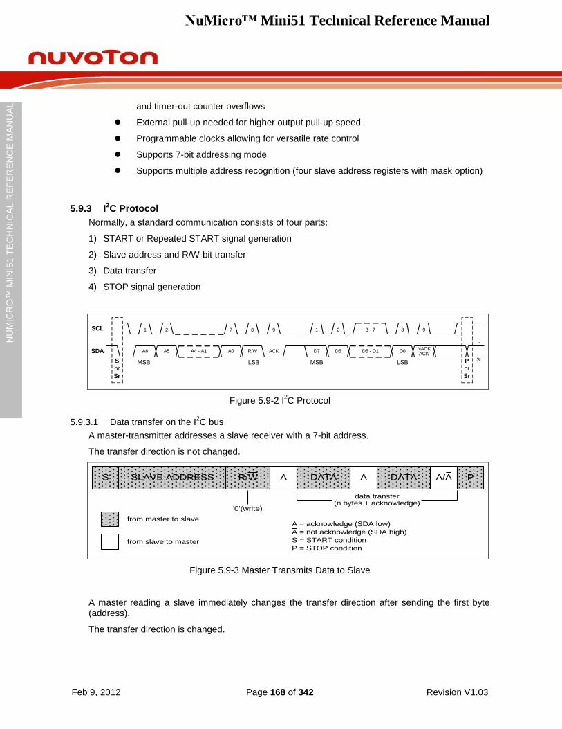
NuMicro™ Mini51 Technical Reference Manual
Feb 9, 2012 Page 168 of 342 Revision V1.03
NU
MIC
RO
™ M
INI5
1 T
EC
HN
ICA
L R
EF
ER
EN
CE
MA
NU
AL
and timer-out counter overflows
External pull-up needed for higher output pull-up speed
Programmable clocks allowing for versatile rate control
Supports 7-bit addressing mode
Supports multiple address recognition (four slave address registers with mask option)
5.9.3 I2C Protocol
Normally, a standard communication consists of four parts:
1) START or Repeated START signal generation
2) Slave address and R/W bit transfer
3) Data transfer
4) STOP signal generation
SCL
SDA
S
or
Sr
MSB
ACK
P
or
Sr
P
SrLSB MSB LSB
1 2 7 8 9 1 2 3 - 7 8 9
A6 A5 A4 - A1 A0 R/W D7 D6 D5 - D1 D0 NACKACK
Figure 5.9-2 I2C Protocol
5.9.3.1 Data transfer on the I2C bus
A master-transmitter addresses a slave receiver with a 7-bit address.
The transfer direction is not changed.
S SLAVE ADDRESS R/W A DATA A DATA A/A P
'0'(write)
data transfer(n bytes + acknowledge)
from master to slave
from slave to master
A = acknowledge (SDA low)
A = not acknowledge (SDA high)
S = START condition
P = STOP condition
Figure 5.9-3 Master Transmits Data to Slave
A master reading a slave immediately changes the transfer direction after sending the first byte (address).
The transfer direction is changed.
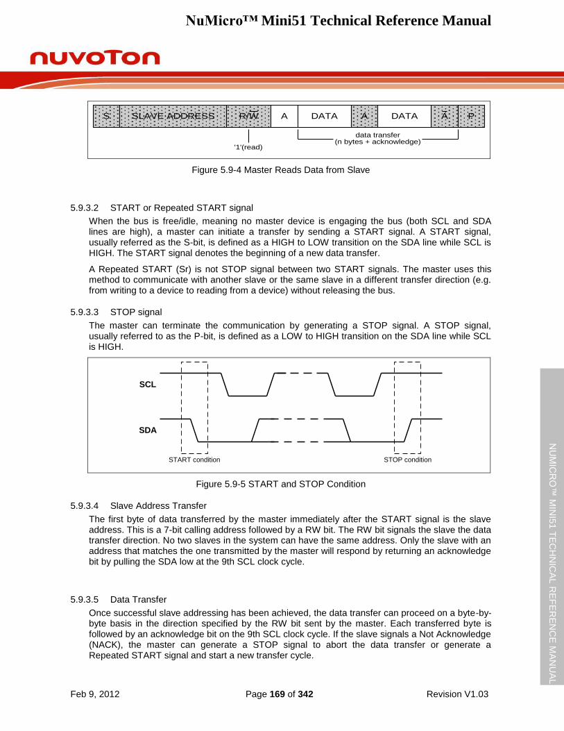
NuMicro™ Mini51 Technical Reference Manual
Feb 9, 2012 Page 169 of 342 Revision V1.03
NU
MIC
RO
™ M
INI5
1 T
EC
HN
ICA
L R
EF
ER
EN
CE
MA
NU
AL
'1'(read)
data transfer(n bytes + acknowledge)
S SLAVE ADDRESS R/W A DATA A DATA A P
Figure 5.9-4 Master Reads Data from Slave
5.9.3.2 START or Repeated START signal
When the bus is free/idle, meaning no master device is engaging the bus (both SCL and SDA lines are high), a master can initiate a transfer by sending a START signal. A START signal, usually referred as the S-bit, is defined as a HIGH to LOW transition on the SDA line while SCL is HIGH. The START signal denotes the beginning of a new data transfer.
A Repeated START (Sr) is not STOP signal between two START signals. The master uses this method to communicate with another slave or the same slave in a different transfer direction (e.g. from writing to a device to reading from a device) without releasing the bus.
5.9.3.3 STOP signal
The master can terminate the communication by generating a STOP signal. A STOP signal, usually referred to as the P-bit, is defined as a LOW to HIGH transition on the SDA line while SCL is HIGH.
START condition STOP condition
SCL
SDA
Figure 5.9-5 START and STOP Condition
5.9.3.4 Slave Address Transfer
The first byte of data transferred by the master immediately after the START signal is the slave address. This is a 7-bit calling address followed by a RW bit. The RW bit signals the slave the data transfer direction. No two slaves in the system can have the same address. Only the slave with an address that matches the one transmitted by the master will respond by returning an acknowledge bit by pulling the SDA low at the 9th SCL clock cycle.
5.9.3.5 Data Transfer
Once successful slave addressing has been achieved, the data transfer can proceed on a byte-by-byte basis in the direction specified by the RW bit sent by the master. Each transferred byte is followed by an acknowledge bit on the 9th SCL clock cycle. If the slave signals a Not Acknowledge (NACK), the master can generate a STOP signal to abort the data transfer or generate a Repeated START signal and start a new transfer cycle.
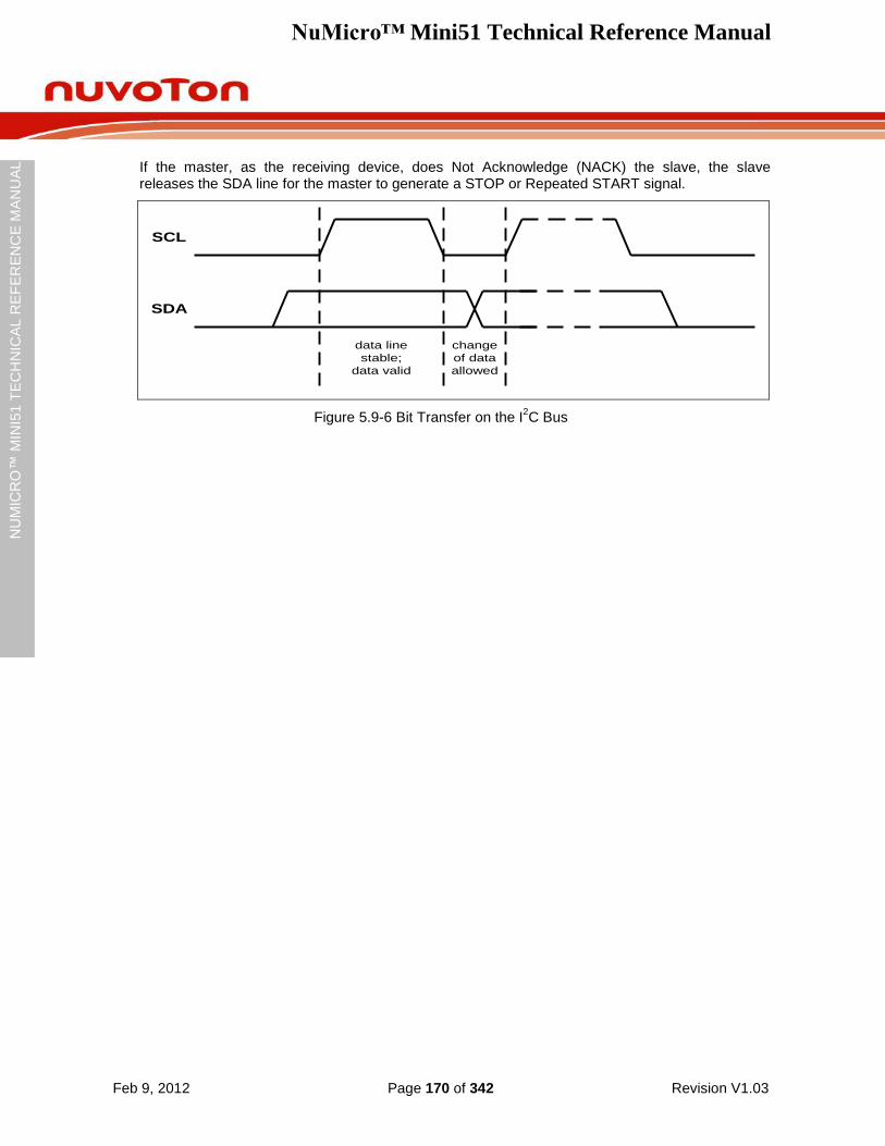
NuMicro™ Mini51 Technical Reference Manual
Feb 9, 2012 Page 170 of 342 Revision V1.03
NU
MIC
RO
™ M
INI5
1 T
EC
HN
ICA
L R
EF
ER
EN
CE
MA
NU
AL
If the master, as the receiving device, does Not Acknowledge (NACK) the slave, the slave releases the SDA line for the master to generate a STOP or Repeated START signal.
data line
stable;
data valid
change
of data
allowed
SCL
SDA
Figure 5.9-6 Bit Transfer on the I2C Bus
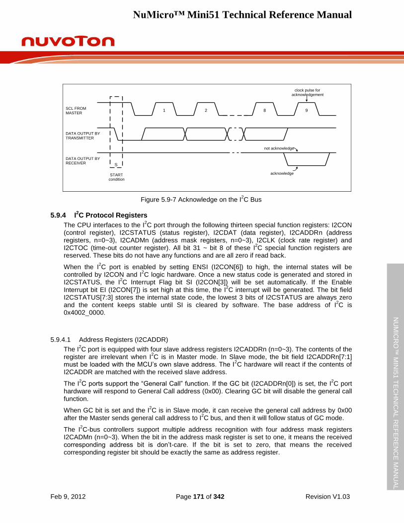
NuMicro™ Mini51 Technical Reference Manual
Feb 9, 2012 Page 171 of 342 Revision V1.03
NU
MIC
RO
™ M
INI5
1 T
EC
HN
ICA
L R
EF
ER
EN
CE
MA
NU
AL
Figure 5.9-7 Acknowledge on the I2C Bus
5.9.4 I2C Protocol Registers
The CPU interfaces to the I2C port through the following thirteen special function registers: I2CON
(control register), I2CSTATUS (status register), I2CDAT (data register), I2CADDRn (address registers, n=0~3), I2CADMn (address mask registers, n=0~3), I2CLK (clock rate register) and I2CTOC (time-out counter register). All bit 31 ~ bit 8 of these I
2C special function registers are
reserved. These bits do not have any functions and are all zero if read back.
When the I2C port is enabled by setting ENSI (I2CON[6]) to high, the internal states will be
controlled by I2CON and I2C logic hardware. Once a new status code is generated and stored in
I2CSTATUS, the I2C Interrupt Flag bit SI (I2CON[3]) will be set automatically. If the Enable
Interrupt bit EI (I2CON[7]) is set high at this time, the I2C interrupt will be generated. The bit field
I2CSTATUS[7:3] stores the internal state code, the lowest 3 bits of I2CSTATUS are always zero and the content keeps stable until SI is cleared by software. The base address of I
2C is
0x4002_0000.
5.9.4.1 Address Registers (I2CADDR)
The I2C port is equipped with four slave address registers I2CADDRn (n=0~3). The contents of the
register are irrelevant when I2C is in Master mode. In Slave mode, the bit field I2CADDRn[7:1]
must be loaded with the MCU‟s own slave address. The I2C hardware will react if the contents of
I2CADDR are matched with the received slave address.
The I2C ports support the “General Call” function. If the GC bit (I2CADDRn[0]) is set, the I
2C port
hardware will respond to General Call address (0x00). Clearing GC bit will disable the general call function.
When GC bit is set and the I2C is in Slave mode, it can receive the general call address by 0x00
after the Master sends general call address to I2C bus, and then it will follow status of GC mode.
The I2C-bus controllers support multiple address recognition with four address mask registers
I2CADMn (n=0~3). When the bit in the address mask register is set to one, it means the received corresponding address bit is don‟t-care. If the bit is set to zero, that means the received corresponding register bit should be exactly the same as address register.
1 2 8 9 SCL FROM MASTER
DATA OUTPUT BY TRANSMITTER
DATA OUTPUT BY RECEIVER S
START condition
clock pulse for acknowledgement
not acknowledge
acknowledge
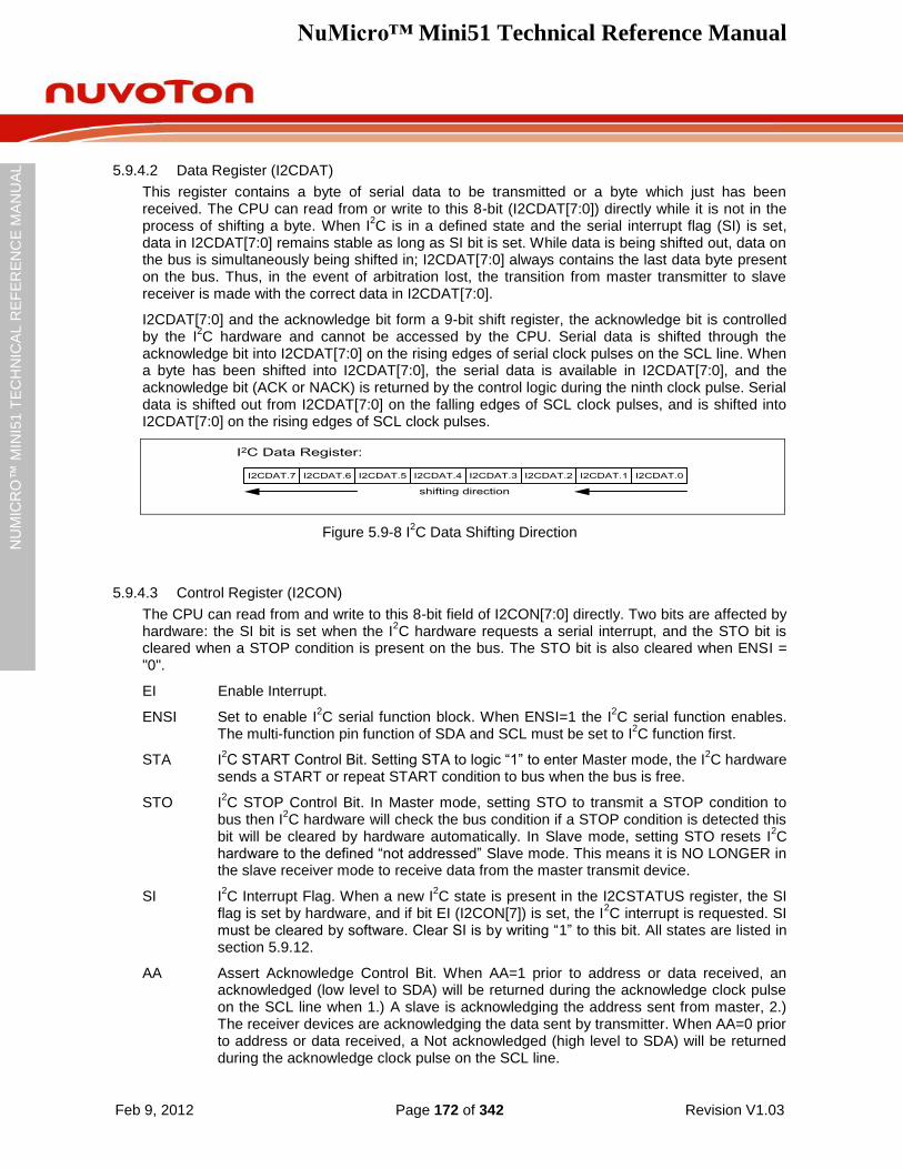
NuMicro™ Mini51 Technical Reference Manual
Feb 9, 2012 Page 172 of 342 Revision V1.03
NU
MIC
RO
™ M
INI5
1 T
EC
HN
ICA
L R
EF
ER
EN
CE
MA
NU
AL
5.9.4.2 Data Register (I2CDAT)
This register contains a byte of serial data to be transmitted or a byte which just has been received. The CPU can read from or write to this 8-bit (I2CDAT[7:0]) directly while it is not in the process of shifting a byte. When I
2C is in a defined state and the serial interrupt flag (SI) is set,
data in I2CDAT[7:0] remains stable as long as SI bit is set. While data is being shifted out, data on the bus is simultaneously being shifted in; I2CDAT[7:0] always contains the last data byte present on the bus. Thus, in the event of arbitration lost, the transition from master transmitter to slave receiver is made with the correct data in I2CDAT[7:0].
I2CDAT[7:0] and the acknowledge bit form a 9-bit shift register, the acknowledge bit is controlled by the I
2C hardware and cannot be accessed by the CPU. Serial data is shifted through the
acknowledge bit into I2CDAT[7:0] on the rising edges of serial clock pulses on the SCL line. When a byte has been shifted into I2CDAT[7:0], the serial data is available in I2CDAT[7:0], and the acknowledge bit (ACK or NACK) is returned by the control logic during the ninth clock pulse. Serial data is shifted out from I2CDAT[7:0] on the falling edges of SCL clock pulses, and is shifted into I2CDAT[7:0] on the rising edges of SCL clock pulses.
I2CDAT.7 I2CDAT.6 I2CDAT.5 I2CDAT.4 I2CDAT.3 I2CDAT.2 I2CDAT.1 I2CDAT.0
I2C Data Register:
shifting direction
Figure 5.9-8 I2C Data Shifting Direction
5.9.4.3 Control Register (I2CON)
The CPU can read from and write to this 8-bit field of I2CON[7:0] directly. Two bits are affected by hardware: the SI bit is set when the I
2C hardware requests a serial interrupt, and the STO bit is
cleared when a STOP condition is present on the bus. The STO bit is also cleared when ENSI = "0".
EI Enable Interrupt.
ENSI Set to enable I2C serial function block. When ENSI=1 the I
2C serial function enables.
The multi-function pin function of SDA and SCL must be set to I2C function first.
STA I2C START Control Bit. Setting STA to logic “1” to enter Master mode, the I
2C hardware
sends a START or repeat START condition to bus when the bus is free.
STO I2C STOP Control Bit. In Master mode, setting STO to transmit a STOP condition to
bus then I2C hardware will check the bus condition if a STOP condition is detected this
bit will be cleared by hardware automatically. In Slave mode, setting STO resets I2C
hardware to the defined “not addressed” Slave mode. This means it is NO LONGER in the slave receiver mode to receive data from the master transmit device.
SI I2C Interrupt Flag. When a new I
2C state is present in the I2CSTATUS register, the SI
flag is set by hardware, and if bit EI (I2CON[7]) is set, the I2C interrupt is requested. SI
must be cleared by software. Clear SI is by writing “1” to this bit. All states are listed in section 5.9.12.
AA Assert Acknowledge Control Bit. When AA=1 prior to address or data received, an acknowledged (low level to SDA) will be returned during the acknowledge clock pulse on the SCL line when 1.) A slave is acknowledging the address sent from master, 2.) The receiver devices are acknowledging the data sent by transmitter. When AA=0 prior to address or data received, a Not acknowledged (high level to SDA) will be returned during the acknowledge clock pulse on the SCL line.
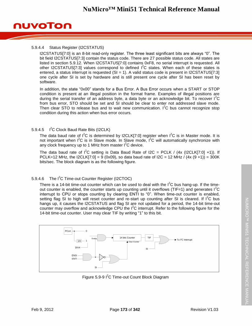
NuMicro™ Mini51 Technical Reference Manual
Feb 9, 2012 Page 173 of 342 Revision V1.03
NU
MIC
RO
™ M
INI5
1 T
EC
HN
ICA
L R
EF
ER
EN
CE
MA
NU
AL
5.9.4.4 Status Register (I2CSTATUS)
I2CSTATUS[7:0] is an 8-bit read-only register. The three least significant bits are always “0”. The bit field I2CSTATUS[7:3] contain the status code. There are 27 possible status code. All states are listed in section 5.9.12. When I2CSTATUS[7:0] contains 0xF8, no serial interrupt is requested. All other I2CSTATUS[7:3] values correspond to defined I
2C states. When each of these states is
entered, a status interrupt is requested (SI = 1). A valid status code is present in I2CSTATUS[7:3] one cycle after SI is set by hardware and is still present one cycle after SI has been reset by software.
In addition, the state “0x00” stands for a Bus Error. A Bus Error occurs when a START or STOP condition is present at an illegal position in the format frame. Examples of illegal positions are during the serial transfer of an address byte, a data byte or an acknowledge bit. To recover I
2C
from bus error, STO should be set and SI should be clear to enter not addressed slave mode. Then clear STO to release bus and to wait new communication. I
2C bus cannot recognize stop
condition during this action when bus error occurs.
5.9.4.5 I2C Clock Baud Rate Bits (I2CLK)
The data baud rate of I2C is determined by I2CLK[7:0] register when I
2C is in Master mode. It is
not important when I2C is in Slave mode. In Slave mode, I
2C will automatically synchronize with
any clock frequency up to 1 MHz from master I2C device.
The data baud rate of I2C setting is Data Baud Rate of I2C = PCLK / (4x (I2CLK[7:0] +1)). If
PCLK=12 MHz, the I2CLK[7:0] = 9 (0x09), so data baud rate of I2C = 12 MHz / (4x (9 +1)) = 300K bits/sec. The block diagram is as the following figure.
5.9.4.6 The I2C Time-out Counter Register (I2CTOC)
There is a 14-bit time-out counter which can be used to deal with the I2C bus hang-up. If the time-
out counter is enabled, the counter starts up counting until it overflows (TIF=1) and generates I2C
interrupt to CPU or stops counting by clearing ENTI to “0”. When time-out counter is enabled, setting flag SI to high will reset counter and re-start up counting after SI is cleared. If I
2C bus
hangs up, it causes the I2CSTATUS and flag SI are not updated for a period, the 14-bit time-out counter may overflow and acknowledge CPU the I
2C interrupt. Refer to the following figure for the
14-bit time-out counter. User may clear TIF by writing “1” to this bit.
1
0PCLK
1/4
14 bits Counter TIF
Clear Counter
ENTI
SIDIV4
ENSI
To I2C InterruptEnable
SI
Figure 5.9-9 I2C Time-out Count Block Diagram
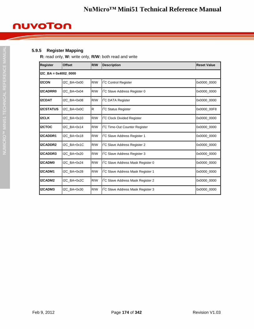
NuMicro™ Mini51 Technical Reference Manual
Feb 9, 2012 Page 174 of 342 Revision V1.03
NU
MIC
RO
™ M
INI5
1 T
EC
HN
ICA
L R
EF
ER
EN
CE
MA
NU
AL
5.9.5 Register Mapping
R: read only, W: write only, R/W: both read and write
Register Offset R/W Description Reset Value
I2C_BA = 0x4002_0000
I2CON I2C_BA+0x00 R/W I2C Control Register 0x0000_0000
I2CADRR0 I2C_BA+0x04 R/W I2C Slave Address Register 0 0x0000_0000
I2CDAT I2C_BA+0x08 R/W I2C DATA Register 0x0000_0000
I2CSTATUS I2C_BA+0x0C R I2C Status Register 0x0000_00F8
I2CLK I2C_BA+0x10 R/W I2C Clock Divided Register 0x0000_0000
I2CTOC I2C_BA+0x14 R/W I2C Time-Out Counter Register 0x0000_0000
I2CADDR1 I2C_BA+0x18 R/W I2C Slave Address Register 1 0x0000_0000
I2CADDR2 I2C_BA+0x1C R/W I2C Slave Address Register 2 0x0000_0000
I2CADDR3 I2C_BA+0x20 R/W I2C Slave Address Register 3 0x0000_0000
I2CADM0 I2C_BA+0x24 R/W I2C Slave Address Mask Register 0 0x0000_0000
I2CADM1 I2C_BA+0x28 R/W I2C Slave Address Mask Register 1 0x0000_0000
I2CADM2 I2C_BA+0x2C R/W I2C Slave Address Mask Register 2 0x0000_0000
I2CADM3 I2C_BA+0x30 R/W I2C Slave Address Mask Register 3 0x0000_0000
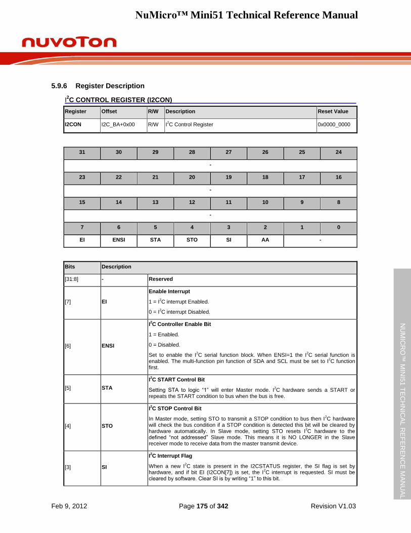
NuMicro™ Mini51 Technical Reference Manual
Feb 9, 2012 Page 175 of 342 Revision V1.03
NU
MIC
RO
™ M
INI5
1 T
EC
HN
ICA
L R
EF
ER
EN
CE
MA
NU
AL
5.9.6 Register Description
I2C CONTROL REGISTER (I2CON)
Register Offset R/W Description Reset Value
I2CON I2C_BA+0x00 R/W I2C Control Register 0x0000_0000
31 30 29 28 27 26 25 24
-
23 22 21 20 19 18 17 16
-
15 14 13 12 11 10 9 8
-
7 6 5 4 3 2 1 0
EI ENSI STA STO SI AA -
Bits Description
[31:8] - Reserved
[7] EI
Enable Interrupt
1 = I2C interrupt Enabled.
0 = I2C interrupt Disabled.
[6] ENSI
I2C Controller Enable Bit
1 = Enabled.
0 = Disabled.
Set to enable the I2C serial function block. When ENSI=1 the I
2C serial function is
enabled. The multi-function pin function of SDA and SCL must be set to I2C function
first.
[5] STA
I2C START Control Bit
Setting STA to logic “1” will enter Master mode. I2C hardware sends a START or
repeats the START condition to bus when the bus is free.
[4] STO
I2C STOP Control Bit
In Master mode, setting STO to transmit a STOP condition to bus then I2C hardware
will check the bus condition if a STOP condition is detected this bit will be cleared by hardware automatically. In Slave mode, setting STO resets I
2C hardware to the
defined “not addressed” Slave mode. This means it is NO LONGER in the Slave receiver mode to receive data from the master transmit device.
[3] SI
I2C Interrupt Flag
When a new I2C state is present in the I2CSTATUS register, the SI flag is set by
hardware, and if bit EI (I2CON[7]) is set, the I2C interrupt is requested. SI must be
cleared by software. Clear SI is by writing “1” to this bit.
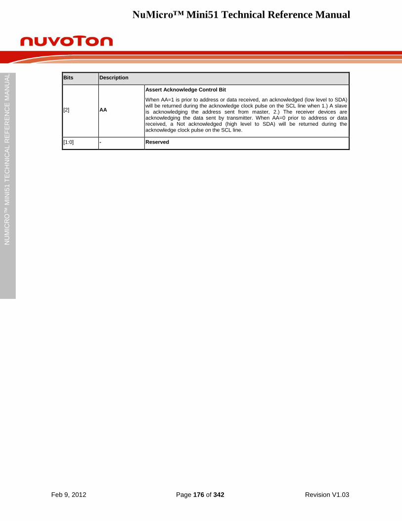
NuMicro™ Mini51 Technical Reference Manual
Feb 9, 2012 Page 176 of 342 Revision V1.03
NU
MIC
RO
™ M
INI5
1 T
EC
HN
ICA
L R
EF
ER
EN
CE
MA
NU
AL
Bits Description
[2] AA
Assert Acknowledge Control Bit
When AA=1 is prior to address or data received, an acknowledged (low level to SDA) will be returned during the acknowledge clock pulse on the SCL line when 1.) A slave is acknowledging the address sent from master, 2.) The receiver devices are acknowledging the data sent by transmitter. When AA=0 prior to address or data received, a Not acknowledged (high level to SDA) will be returned during the acknowledge clock pulse on the SCL line.
[1:0] - Reserved
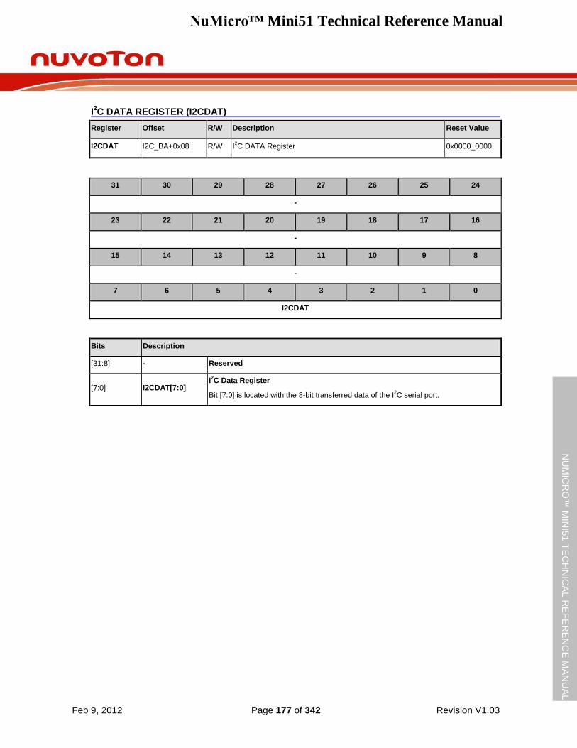
NuMicro™ Mini51 Technical Reference Manual
Feb 9, 2012 Page 177 of 342 Revision V1.03
NU
MIC
RO
™ M
INI5
1 T
EC
HN
ICA
L R
EF
ER
EN
CE
MA
NU
AL
I2C DATA REGISTER (I2CDAT)
Register Offset R/W Description Reset Value
I2CDAT I2C_BA+0x08 R/W I2C DATA Register 0x0000_0000
31 30 29 28 27 26 25 24
-
23 22 21 20 19 18 17 16
-
15 14 13 12 11 10 9 8
-
7 6 5 4 3 2 1 0
I2CDAT
Bits Description
[31:8] - Reserved
[7:0] I2CDAT[7:0] I2C Data Register
Bit [7:0] is located with the 8-bit transferred data of the I2C serial port.
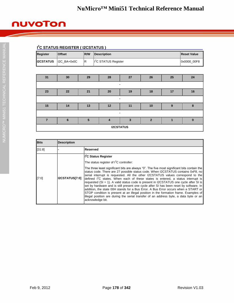
NuMicro™ Mini51 Technical Reference Manual
Feb 9, 2012 Page 178 of 342 Revision V1.03
NU
MIC
RO
™ M
INI5
1 T
EC
HN
ICA
L R
EF
ER
EN
CE
MA
NU
AL
I2C STATUS REGISTER ( I2CSTATUS )
Register Offset R/W Description Reset Value
I2CSTATUS I2C_BA+0x0C R I2C STATUS Register 0x0000_00F8
31 30 29 28 27 26 25 24
-
23 22 21 20 19 18 17 16
-
15 14 13 12 11 10 9 8
-
7 6 5 4 3 2 1 0
I2CSTATUS
Bits Description
[31:8] - Reserved
[7:0] I2CSTATUS[7:0]
I2C Status Register
The status register of I2C controller:
The three least significant bits are always “0”. The five most significant bits contain the status code. There are 27 possible status code. When I2CSTATUS contains 0xF8, no serial interrupt is requested. All the other I2CSTATUS values correspond to the defined I
2C states. When each of these states is entered, a status interrupt is
requested (SI = 1). A valid status code is present in I2CSTATUS one cycle after SI is set by hardware and is still present one cycle after SI has been reset by software. In addition, the state 00H stands for a Bus Error. A Bus Error occurs when a START or STOP condition is present at an illegal position in the formation frame. Examples of illegal position are during the serial transfer of an address byte, a data byte or an acknowledge bit.
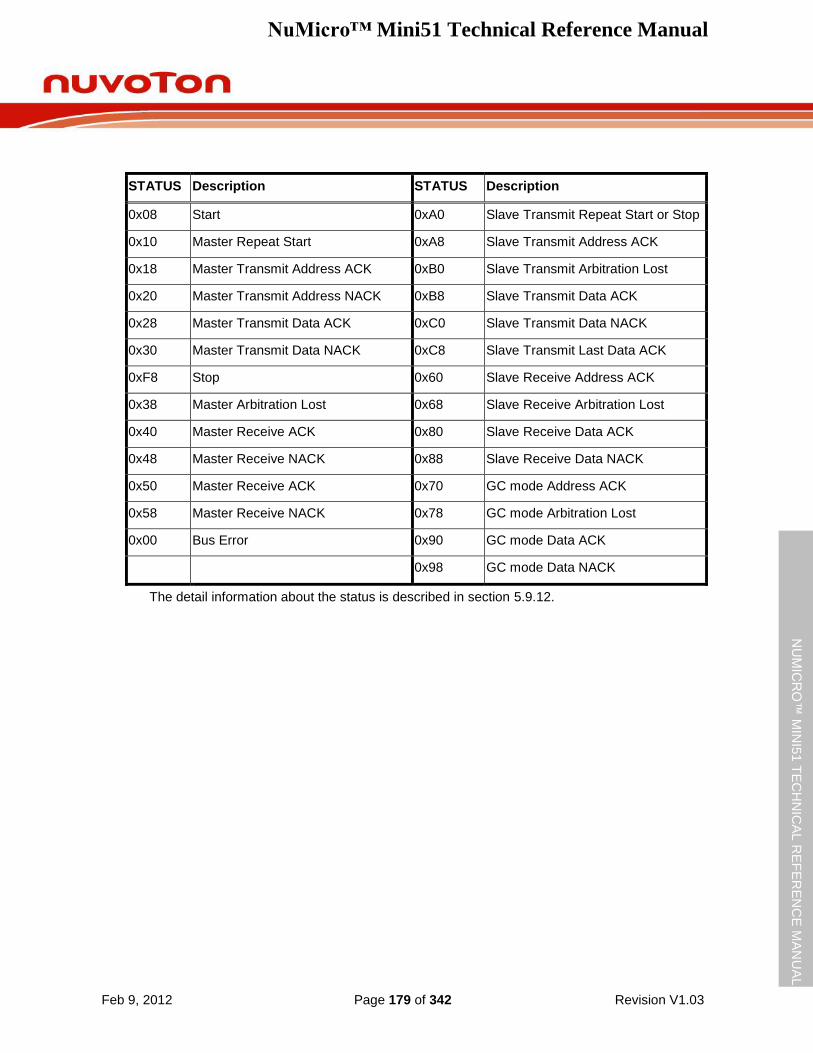
NuMicro™ Mini51 Technical Reference Manual
Feb 9, 2012 Page 179 of 342 Revision V1.03
NU
MIC
RO
™ M
INI5
1 T
EC
HN
ICA
L R
EF
ER
EN
CE
MA
NU
AL
STATUS Description STATUS Description
0x08 Start 0xA0 Slave Transmit Repeat Start or Stop
0x10 Master Repeat Start 0xA8 Slave Transmit Address ACK
0x18 Master Transmit Address ACK 0xB0 Slave Transmit Arbitration Lost
0x20 Master Transmit Address NACK 0xB8 Slave Transmit Data ACK
0x28 Master Transmit Data ACK 0xC0 Slave Transmit Data NACK
0x30 Master Transmit Data NACK 0xC8 Slave Transmit Last Data ACK
0xF8 Stop 0x60 Slave Receive Address ACK
0x38 Master Arbitration Lost 0x68 Slave Receive Arbitration Lost
0x40 Master Receive ACK 0x80 Slave Receive Data ACK
0x48 Master Receive NACK 0x88 Slave Receive Data NACK
0x50 Master Receive ACK 0x70 GC mode Address ACK
0x58 Master Receive NACK 0x78 GC mode Arbitration Lost
0x00 Bus Error 0x90 GC mode Data ACK
0x98 GC mode Data NACK
The detail information about the status is described in section 5.9.12.
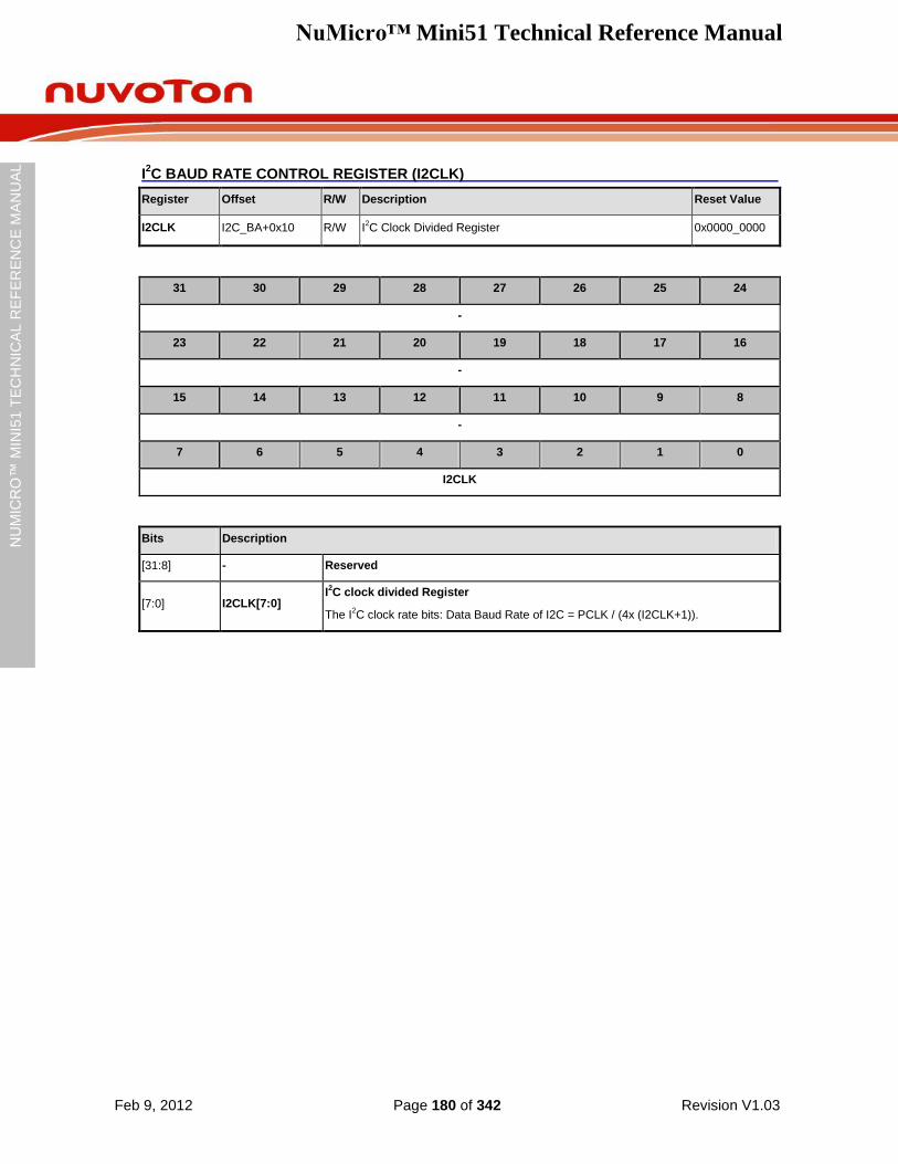
NuMicro™ Mini51 Technical Reference Manual
Feb 9, 2012 Page 180 of 342 Revision V1.03
NU
MIC
RO
™ M
INI5
1 T
EC
HN
ICA
L R
EF
ER
EN
CE
MA
NU
AL
I2C BAUD RATE CONTROL REGISTER (I2CLK)
Register Offset R/W Description Reset Value
I2CLK I2C_BA+0x10 R/W I2C Clock Divided Register 0x0000_0000
31 30 29 28 27 26 25 24
-
23 22 21 20 19 18 17 16
-
15 14 13 12 11 10 9 8
-
7 6 5 4 3 2 1 0
I2CLK
Bits Description
[31:8] - Reserved
[7:0] I2CLK[7:0] I2C clock divided Register
The I2C clock rate bits: Data Baud Rate of I2C = PCLK / (4x (I2CLK+1)).
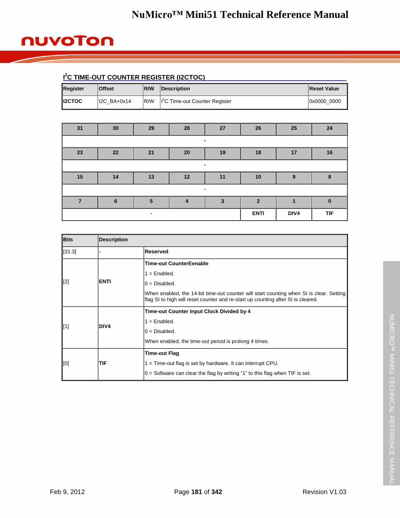
NuMicro™ Mini51 Technical Reference Manual
Feb 9, 2012 Page 181 of 342 Revision V1.03
NU
MIC
RO
™ M
INI5
1 T
EC
HN
ICA
L R
EF
ER
EN
CE
MA
NU
AL
I2C TIME-OUT COUNTER REGISTER (I2CTOC)
Register Offset R/W Description Reset Value
I2CTOC I2C_BA+0x14 R/W I2C Time-out Counter Register 0x0000_0000
31 30 29 28 27 26 25 24
-
23 22 21 20 19 18 17 16
-
15 14 13 12 11 10 9 8
-
7 6 5 4 3 2 1 0
- ENTI DIV4 TIF
Bits Description
[31:3] - Reserved
[2] ENTI
Time-out CounterEenable
1 = Enabled.
0 = Disabled.
When enabled, the 14-bit time-out counter will start counting when SI is clear. Setting flag SI to high will reset counter and re-start up counting after SI is cleared.
[1] DIV4
Time-out Counter Input Clock Divided by 4
1 = Enabled.
0 = Disabled.
When enabled, the time-out period is prolong 4 times.
[0] TIF
Time-out Flag
1 = Time-out flag is set by hardware. It can interrupt CPU.
0 = Software can clear the flag by writing “1” to this flag when TIF is set.
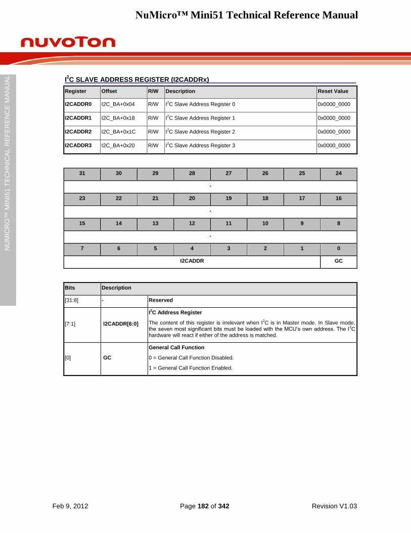
NuMicro™ Mini51 Technical Reference Manual
Feb 9, 2012 Page 182 of 342 Revision V1.03
NU
MIC
RO
™ M
INI5
1 T
EC
HN
ICA
L R
EF
ER
EN
CE
MA
NU
AL
I2C SLAVE ADDRESS REGISTER (I2CADDRx)
Register Offset R/W Description Reset Value
I2CADDR0 I2C_BA+0x04 R/W I2C Slave Address Register 0 0x0000_0000
I2CADDR1 I2C_BA+0x18 R/W I2C Slave Address Register 1 0x0000_0000
I2CADDR2 I2C_BA+0x1C R/W I2C Slave Address Register 2 0x0000_0000
I2CADDR3 I2C_BA+0x20 R/W I2C Slave Address Register 3 0x0000_0000
31 30 29 28 27 26 25 24
-
23 22 21 20 19 18 17 16
-
15 14 13 12 11 10 9 8
-
7 6 5 4 3 2 1 0
I2CADDR GC
Bits Description
[31:8] - Reserved
[7:1] I2CADDR[6:0]
I2C Address Register
The content of this register is irrelevant when I2C is in Master mode. In Slave mode,
the seven most significant bits must be loaded with the MCU‟s own address. The I2C
hardware will react if either of the address is matched.
[0] GC
General Call Function
0 = General Call Function Disabled.
1 = General Call Function Enabled.
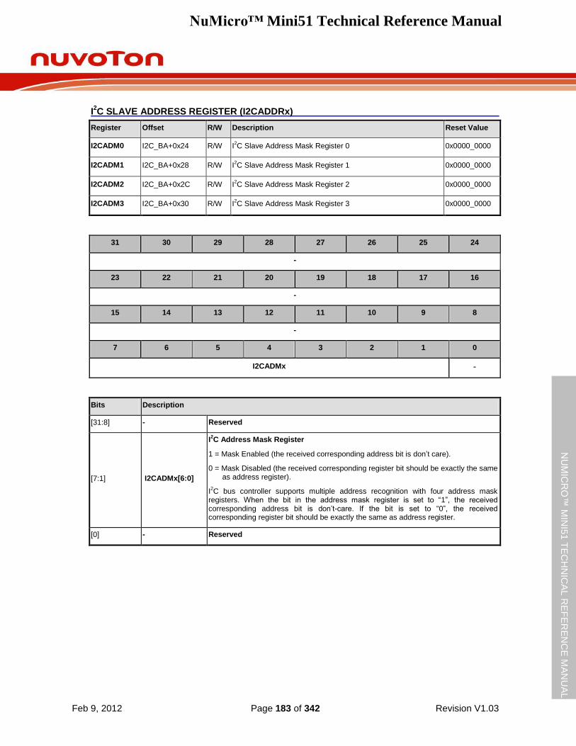
NuMicro™ Mini51 Technical Reference Manual
Feb 9, 2012 Page 183 of 342 Revision V1.03
NU
MIC
RO
™ M
INI5
1 T
EC
HN
ICA
L R
EF
ER
EN
CE
MA
NU
AL
I2C SLAVE ADDRESS REGISTER (I2CADDRx)
Register Offset R/W Description Reset Value
I2CADM0 I2C_BA+0x24 R/W I2C Slave Address Mask Register 0 0x0000_0000
I2CADM1 I2C_BA+0x28 R/W I2C Slave Address Mask Register 1 0x0000_0000
I2CADM2 I2C_BA+0x2C R/W I2C Slave Address Mask Register 2 0x0000_0000
I2CADM3 I2C_BA+0x30 R/W I2C Slave Address Mask Register 3 0x0000_0000
31 30 29 28 27 26 25 24
-
23 22 21 20 19 18 17 16
-
15 14 13 12 11 10 9 8
-
7 6 5 4 3 2 1 0
I2CADMx -
Bits Description
[31:8] - Reserved
[7:1] I2CADMx[6:0]
I2C Address Mask Register
1 = Mask Enabled (the received corresponding address bit is don‟t care).
0 = Mask Disabled (the received corresponding register bit should be exactly the same as address register).
I2C bus controller supports multiple address recognition with four address mask
registers. When the bit in the address mask register is set to “1”, the received corresponding address bit is don‟t-care. If the bit is set to “0”, the received corresponding register bit should be exactly the same as address register.
[0] - Reserved
NuMicro™ Mini51 Technical Reference Manual
Feb 9, 2012 Page 184 of 342 Revision V1.03
NU
MIC
RO
™ M
INI5
1 T
EC
HN
ICA
L R
EF
ER
EN
CE
MA
NU
AL
5.9.7 Operation Modes
The on-chip I2C port supports five operation modes: Master transmitter, Master receiver, Slave
transmitter, Slave receiver, and GC call.
In a given application, I2C port may operate as a master or as a slave. In Slave mode, the I
2C port
hardware looks for its own slave address and the general call address. If one of these addresses is detected, and if the slave is willing to receive or transmit data from/to master (by setting the AA bit), acknowledge pulse will be transmitted out on the 9th clock, hence an interrupt is requested on both master and slave devices if interrupt is enabled. When the microcontroller wishes to become the bus master, the hardware waits until the bus is free before the Master mode is entered so that a possible slave action is not interrupted. If bus arbitration is lost in Master mode, I
2C port switches
to Slave mode immediately and can detect its own slave address in the same serial transfer.
5.9.8 Master Transmitter Mode
Serial data is output through SDA while SCL outputs the serial clock. The first byte transmitted contains the slave address of the receiving device (7 bits) and the data direction bit. In this case the data direction bit (R/W) will be logic “0”, and it is represented by “W” in the flow diagrams. Thus the first byte transmitted is SLA+W. Serial data transmits 8 bits at a time. After each byte is transmitted, an acknowledge bit is received. The START and STOP conditions are output to indicate the beginning and end of a serial transfer.
5.9.9 Master Receiver Mode
In this case the data direction bit (R/W) will be logic “1”, and it is represented by “R” in the flow diagrams. Thus the first byte transmitted is SLA+R. Serial data is received via SDA while SCL outputs the serial clock. Serial data receives 8 bits at a time. After each byte is received, an acknowledge bit is transmitted. The START and STOP conditions are output to indicate the beginning and end of a serial transfer.
5.9.10 Slave Receiver Mode
Serial data and serial clock are received through SDA and SCL. After each byte is received, an acknowledge bit is transmitted. START and STOP conditions are recognized as the beginning and end of a serial transfer. Address recognition is performed by hardware after reception of the slave address and direction bit.
5.9.11 Slave Transmitter Mode
The first byte is received and handled as in the slave receiver mode. However, in this mode, the direction bit will indicate that the transfer direction is reversed. Serial data is transmitted via SDA while the serial clock is input through SCL. START and STOP conditions are recognized as the beginning and end of a serial transfer.
5.9.12 Data Transfer Flow in Five Operation Modes
The five operation modes are: Master transmitter, Master receiver, Slave transmitter, Slave receiver, and GC Call. Bits STA, STO and AA in I2CON register will determine the next state of the I2C hardware after SI flag is cleared. Upon completion of the new action, a new status code will be
updated and the SI flag will be set. If the I2C interrupt control bit EI (I2CON[7]) is set, appropriate
action or software branch of the new status code can be performed in the Interrupt service routine.
Data transfers in each mode are shown in the following figures.
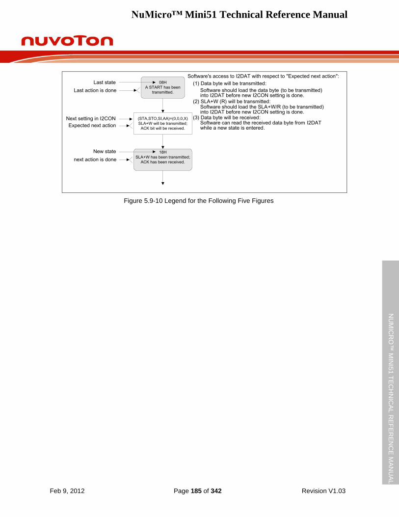
NuMicro™ Mini51 Technical Reference Manual
Feb 9, 2012 Page 185 of 342 Revision V1.03
NU
MIC
RO
™ M
INI5
1 T
EC
HN
ICA
L R
EF
ER
EN
CE
MA
NU
AL
08H
A START has been
transmitted.
(STA,STO,SI,AA)=(0,0,0,X)
SLA+W will be transmitted;
ACK bit will be received.
18H
SLA+W has been transmitted;
ACK has been received.
Last state
Last action is done
Next setting in I2CON
Expected next action
next action is done
New state
Software's access to I2DAT with respect to "Expected next action":
Software should load the data byte (to be transmitted)into I2DAT before new I2CON setting is done.
(1) Data byte will be transmitted:
(2) SLA+W (R) will be transmitted:Software should load the SLA+W/R (to be transmitted)into I2DAT before new I2CON setting is done.
(3) Data byte will be received:Software can read the received data byte from I2DATwhile a new state is entered.
Figure 5.9-10 Legend for the Following Five Figures
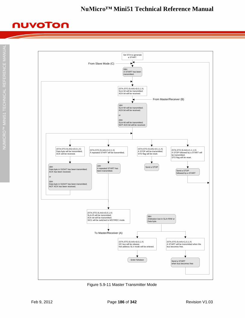
NuMicro™ Mini51 Technical Reference Manual
Feb 9, 2012 Page 186 of 342 Revision V1.03
NU
MIC
RO
™ M
INI5
1 T
EC
HN
ICA
L R
EF
ER
EN
CE
MA
NU
AL
08H
A START has been
transmitted.
(STA,STO,SI,AA)=(0,0,1,X)
SLA+W will be transmitted;
ACK bit will be received.
Set STA to generate
a START.
18H
SLA+W will be transmitted;
ACK bit will be received.
or
20H
SLA+W will be transmitted;
NOT ACK bit will be received.
(STA,STO,SI,AA)=(1,0,1,X)
A repeated START will be transmitted;
(STA,STO,SI,AA)=(0,0,1,X)
Data byte will be transmitted;
ACK will be received.
(STA,STO,SI,AA)=(0,1,1,X)
A STOP will be transmitted;
STO flag will be reset.
Send a STOP
(STA,STO,SI,AA)=(1,1,1,X)
A STOP followed by a START will
be transmitted;
STO flag will be reset.
Send a STOP
followed by a START
28H
Data byte in S1DAT has been transmitted;
ACK has been received.
or
30H
Data byte in S1DAT has been transmitted;
NOT ACK has been received.
10H
A repeated START has
been transmitted.
(STA,STO,SI,AA)=(0,0,1,X)
SLA+R will be transmitted;
ACK bit will be transmitted;
SIO1 will be switched to MST/REC mode.
38H
Arbitration lost in SLA+R/W or
Data byte.
(STA,STO,SI,AA)=(0,0,1,X)
I2C bus will be release;
Not address SLV mode will be entered.
(STA,STO,SI,AA)=(1,0,1,X)
A START will be transmitted when the
bus becomes free.
Send a START
when bus becomes free
Enter NAslave
From Slave Mode (C)
To Master/Receiver (A)
From Master/Receiver (B)
Figure 5.9-11 Master Transmitter Mode
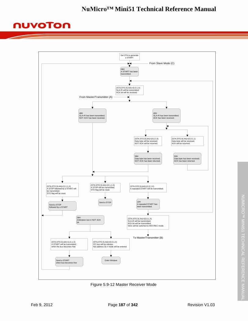
NuMicro™ Mini51 Technical Reference Manual
Feb 9, 2012 Page 187 of 342 Revision V1.03
NU
MIC
RO
™ M
INI5
1 T
EC
HN
ICA
L R
EF
ER
EN
CE
MA
NU
AL
08H
A START has been
transmitted.
(STA,STO,SI,AA)=(0,0,1,X)
SLA+R will be transmitted;
ACK bit will be received.
Set STA to generate
a START.
40H
SLA+R has been transmitted;
ACK has been received.
(STA,STO,SI,AA)=(0,1,1,X)
A STOP will be transmitted;
STO flag will be reset.
(STA,STO,SI,AA)=(1,1,1,X)
A STOP followed by a START will
be transmitted;
STO flag will be reset.
(STA,STO,SI,AA)=(0,0,1,0)
Data byte will be received;
NOT ACK will be returned.
Send a STOP
(STA,STO,SI,AA)=(0,0,1,1)
Data byte will be received;
ACK will be returned.
10H
A repeated START has
been transmitted.
(STA,STO,SI,AA)=(0,0,1,X)
SLA+R will be transmitted;
ACK bit will be transmitted;
SIO1 will be switched to MST/REC mode.
(STA,STO,SI,AA)=(1,0,1,X)
A START will be transmitted;
when the bus becomes free
(STA,STO,SI,AA)=(0,0,1,X)
I2C bus will be release;
Not address SLV mode will be entered.
Enter NAslave
From Master/Transmitter (A)
To Master/Transmitter (B)
From Slave Mode (C)
48H
SLA+R has been transmitted;
NOT ACK has been received.
58H
Data byte has been received;
NOT ACK has been returned.
50H
Data byte has been received;
ACK has been returned.
Send a STOP
followed by a START
38H
Arbitration lost in NOT ACK
bit.
Send a START
when bus becomes free
(STA,STO,SI,AA)=(1,0,1,X)
A repeated START will be transmitted;
Figure 5.9-12 Master Receiver Mode
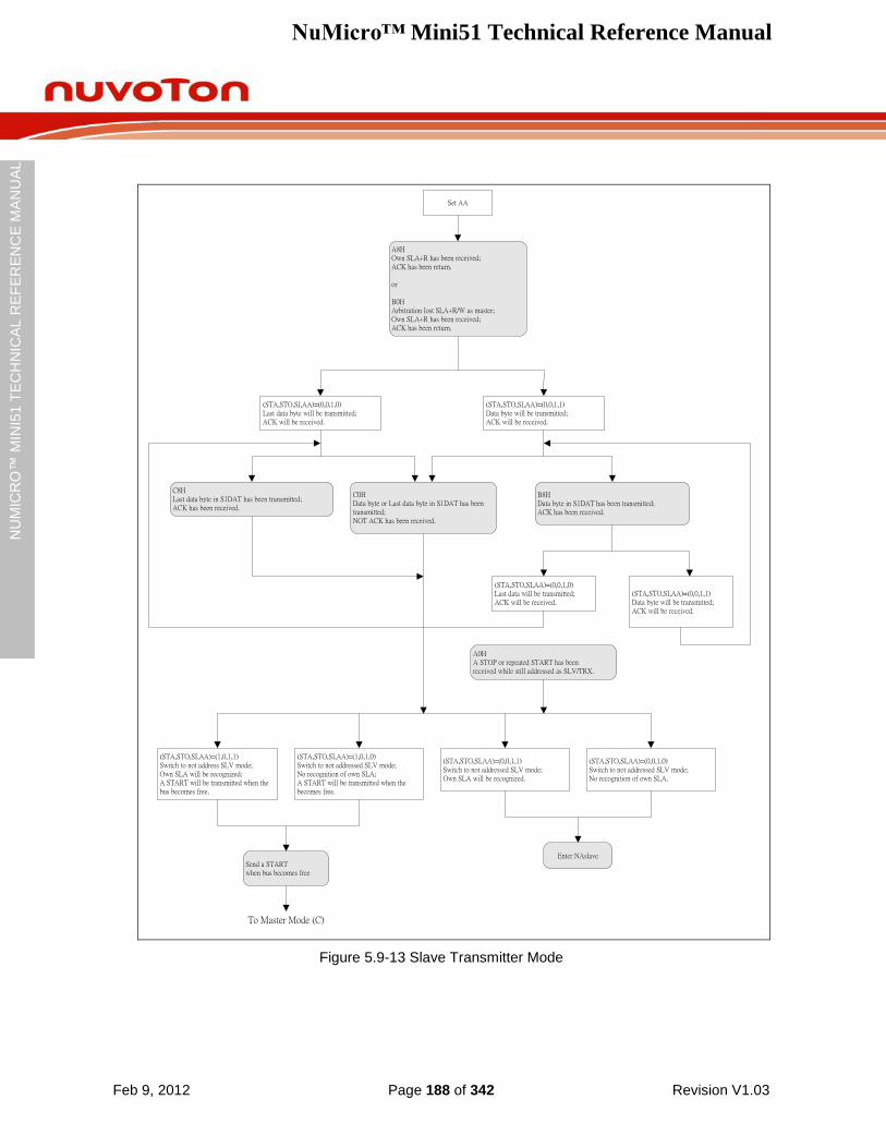
NuMicro™ Mini51 Technical Reference Manual
Feb 9, 2012 Page 188 of 342 Revision V1.03
NU
MIC
RO
™ M
INI5
1 T
EC
HN
ICA
L R
EF
ER
EN
CE
MA
NU
AL
Set AA
A8HOwn SLA+R has been received;ACK has been return.
or
B0HArbitration lost SLA+R/W as master;Own SLA+R has been received;ACK has been return.
(STA,STO,SI,AA)=(1,0,1,1)Switch to not address SLV mode;Own SLA will be recognized;A START will be transmitted when the bus becomes free.
(STA,STO,SI,AA)=(0,0,1,0)Last data will be transmitted;ACK will be received.
(STA,STO,SI,AA)=(0,0,1,1)Data byte will be transmitted;ACK will be received.
Send a STARTwhen bus becomes free
C8HLast data byte in S1DAT has been transmitted;ACK has been received.
(STA,STO,SI,AA)=(1,0,1,0)Switch to not addressed SLV mode;No recognition of own SLA;A START will be transmitted when the becomes free.
(STA,STO,SI,AA)=(0,0,1,1)Switch to not addressed SLV mode;Own SLA will be recognized.
(STA,STO,SI,AA)=(0,0,1,0)Switch to not addressed SLV mode;No recognition of own SLA.
Enter NAslave
To Master Mode (C)
(STA,STO,SI,AA)=(0,0,1,0)Last data byte will be transmitted;ACK will be received.
(STA,STO,SI,AA)=(0,0,1,1)Data byte will be transmitted;ACK will be received.
C0HData byte or Last data byte in S1DAT has been transmitted;NOT ACK has been received.
B8HData byte in S1DAT has been transmitted;ACK has been received.
A0HA STOP or repeated START has beenreceived while still addressed as SLV/TRX.
Figure 5.9-13 Slave Transmitter Mode
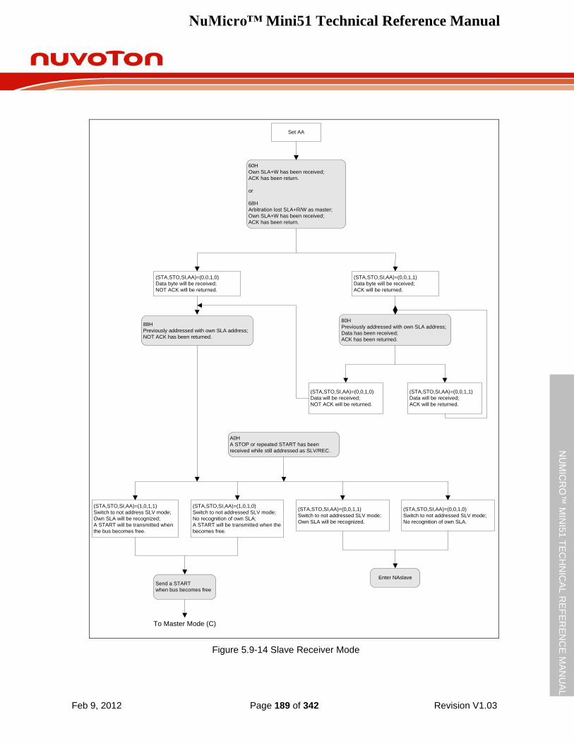
NuMicro™ Mini51 Technical Reference Manual
Feb 9, 2012 Page 189 of 342 Revision V1.03
NU
MIC
RO
™ M
INI5
1 T
EC
HN
ICA
L R
EF
ER
EN
CE
MA
NU
AL
Set AA
60H
Own SLA+W has been received;
ACK has been return.
or
68H
Arbitration lost SLA+R/W as master;
Own SLA+W has been received;
ACK has been return.
(STA,STO,SI,AA)=(1,0,1,1)
Switch to not address SLV mode;
Own SLA will be recognized;
A START will be transmitted when
the bus becomes free.
(STA,STO,SI,AA)=(0,0,1,0)
Data will be received;
NOT ACK will be returned.
(STA,STO,SI,AA)=(0,0,1,1)
Data will be received;
ACK will be returned.
Send a START
when bus becomes free
88H
Previously addressed with own SLA address;
NOT ACK has been returned.
(STA,STO,SI,AA)=(1,0,1,0)
Switch to not addressed SLV mode;
No recognition of own SLA;
A START will be transmitted when the
becomes free.
(STA,STO,SI,AA)=(0,0,1,1)
Switch to not addressed SLV mode;
Own SLA will be recognized.
(STA,STO,SI,AA)=(0,0,1,0)
Switch to not addressed SLV mode;
No recognition of own SLA.
Enter NAslave
To Master Mode (C)
(STA,STO,SI,AA)=(0,0,1,0)
Data byte will be received;
NOT ACK will be returned.
(STA,STO,SI,AA)=(0,0,1,1)
Data byte will be received;
ACK will be returned.
80H
Previously addressed with own SLA address;
Data has been received;
ACK has been returned.
A0H
A STOP or repeated START has been
received while still addressed as SLV/REC.
Figure 5.9-14 Slave Receiver Mode
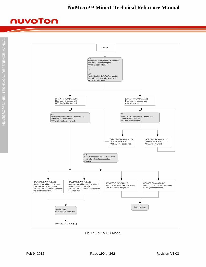
NuMicro™ Mini51 Technical Reference Manual
Feb 9, 2012 Page 190 of 342 Revision V1.03
NU
MIC
RO
™ M
INI5
1 T
EC
HN
ICA
L R
EF
ER
EN
CE
MA
NU
AL
Set AA
70H
Reception of the general call address
and one or more data bytes;
ACK has been return.
or
78H
Arbitration lost SLA+R/W as master;
and address as SLA by general call;
ACK has been return.
(STA,STO,SI,AA)=(1,0,1,1)
Switch to not address SLV mode;
Own SLA will be recognized;
A START will be transmitted when
the bus becomes free.
(STA,STO,SI,AA)=(X,0,1,0)
Data will be received;
NOT ACK will be returned.
(STA,STO,SI,AA)=(X,0,1,1)
Data will be received;
ACK will be returned.
Send a START
when bus becomes free
98H
Previously addressed with General Call;
Data byte has been received;
NOT ACK has been returned.
(STA,STO,SI,AA)=(1,0,1,0)
Switch to not addressed SLV mode;
No recognition of own SLA;
A START will be transmitted when the
becomes free.
(STA,STO,SI,AA)=(0,0,1,1)
Switch to not addressed SLV mode;
Own SLA will be recognized.
(STA,STO,SI,AA)=(0,0,1,0)
Switch to not addressed SLV mode;
No recognition of own SLA.
Enter NAslave
To Master Mode (C)
(STA,STO,SI,AA)=(X,0,1,0)
Data byte will be received;
NOT ACK will be returned.
(STA,STO,SI,AA)=(X,0,1,1)
Data byte will be received;
ACK will be returned.
90H
Previously addressed with General Call;
Data has been received;
ACK has been returned.
A0H
A STOP or repeated START has been
received while still addressed as
SLV/REC.
Figure 5.9-15 GC Mode

NuMicro™ Mini51 Technical Reference Manual
Feb 9, 2012 Page 191 of 342 Revision V1.03
NU
MIC
RO
™ M
INI5
1 T
EC
HN
ICA
L R
EF
ER
EN
CE
MA
NU
AL
5.10 Enhanced PWM Generator
5.10.1 Overview
The NuMicro Mini51 series has built one PWM unit which is specially designed for motor driving control applications. The PWM unit supports 6 PWM generators which can be configured as 6 independent PWM outputs, PWM0~PWM5, or as 3 complementary PWM pairs, (PWM0, PWM1), (PWM2, PWM3) and (PWM4, PWM5) with 3 programmable dead-zone generators.
Each PWM generator shares the 8-bit prescaler, clock divider providing 5 divided frequencies (1, 1/2, 1/4, 1/8, 1/16). Each PWM output has independent 16-bit counter for PWM period control, and 16-bit comparators for PWM duty control. The 6 PWM generators provide six independent PWM interrupt flags which are set by hardware when the corresponding PWM period counter comparison matched. Each PWM interrupt source with its corresponding enable bit can request PWM interrupt. The PWM generators can be configured as One-shot mode to produce only one PWM cycle signal or Auto-reload mode to output PWM waveform continuously.
5.10.2 Features
The PWM unit supports the following features:
Six independent 16-bit PWM duty control units with maximum 6 port pins:
6 independent PWM outputs – PWM0, PWM1, PWM2, PWM3, PWM4, and PWM5
3 complementary PWM pairs, with each pin in a pair mutually complement to each other and capable of programmable dead-zone insertion – (PWM0, PWM1), (PWM2, PWM3) and (PWM4, PWM5)
3 synchronous PWM pairs, with each pin in a pair in-phase – (PWM0, PWM1), (PWM2, PWM3) and (PWM4, PWM5)
Group control bit – PWM2 and PWM4 are synchronized with PWM0
One-shot (only support edge alignment mode) or Auto-reload mode PWM
Up to 16-bit resolution
Supports Edge-aligned and Center-aligned mode
Programmable dead-zone insertion between complementary paired PWMs
Each pin of PWM0 to PWM5 has independent polarity setting control
Hardware fault brake protections
Two Interrupt source types:
Synchronously requested at PWM frequency when down counter comparison matched (edge- and center-aligned mode) or underflow (edge- aligned mode)
Requested when external fault brake asserted
BKP0: EINT0
BKP1: EINT1 or CPO0
The PWM signals before polarity control stage are defined in view of positive logic. Whether the PWM ports are active high or active low is controlled by the polarity control register.
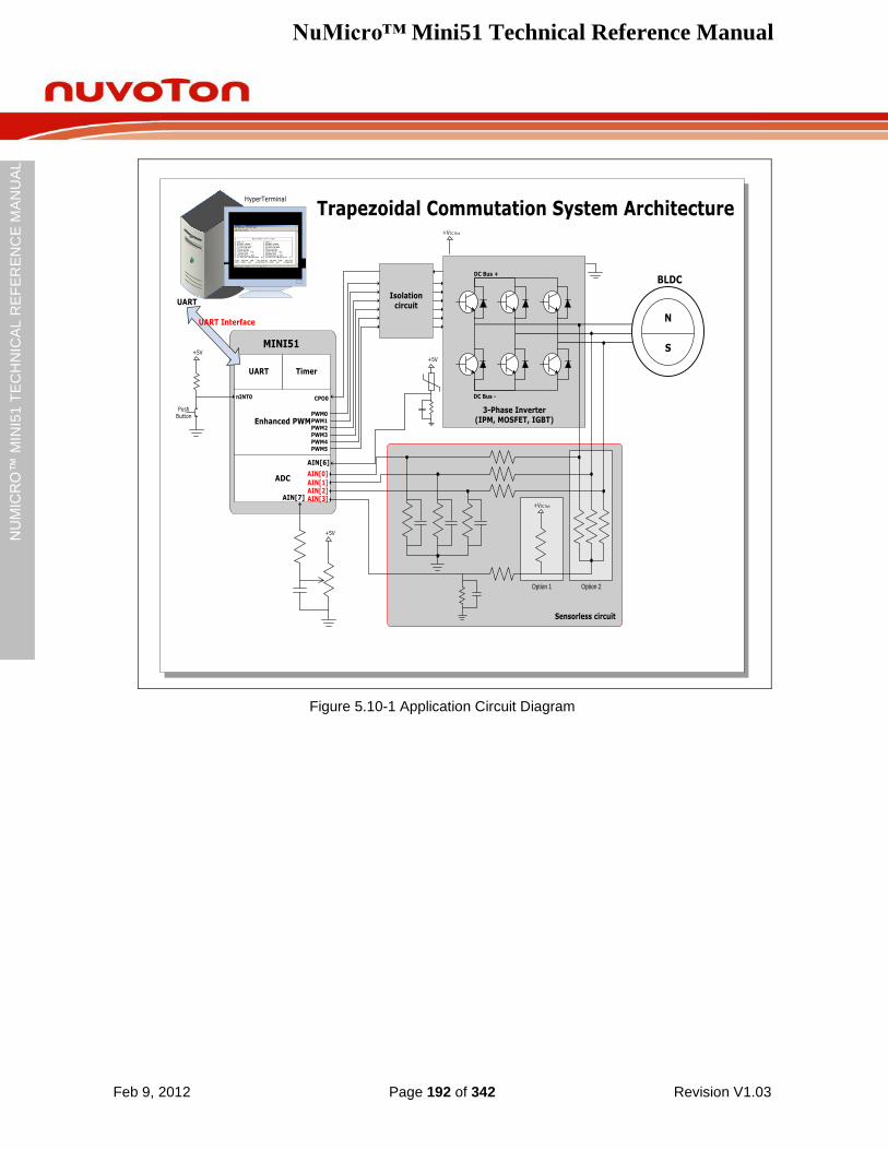
NuMicro™ Mini51 Technical Reference Manual
Feb 9, 2012 Page 192 of 342 Revision V1.03
NU
MIC
RO
™ M
INI5
1 T
EC
HN
ICA
L R
EF
ER
EN
CE
MA
NU
AL
Figure 5.10-1 Application Circuit Diagram
ADC
Enhanced PWM
UART Timer
HyperTerminal
UART
UART Interface
3-Phase Inverter(IPM, MOSFET, IGBT)
Isolation circuit
DC Bus +
DC Bus -
BLDC
S
N
+5V
AIN[7]
+5V
PWM0PWM1PWM2PWM3PWM4PWM5
AIN[6]
nINT0
Push Button
+5V
CPO0
+VDC Bus
MINI51
Trapezoidal Commutation System Architecture
AIN[0]
AIN[1]AIN[2]AIN[3]
+VDC Bus
Option 1 Option 2
Sensorless circuit
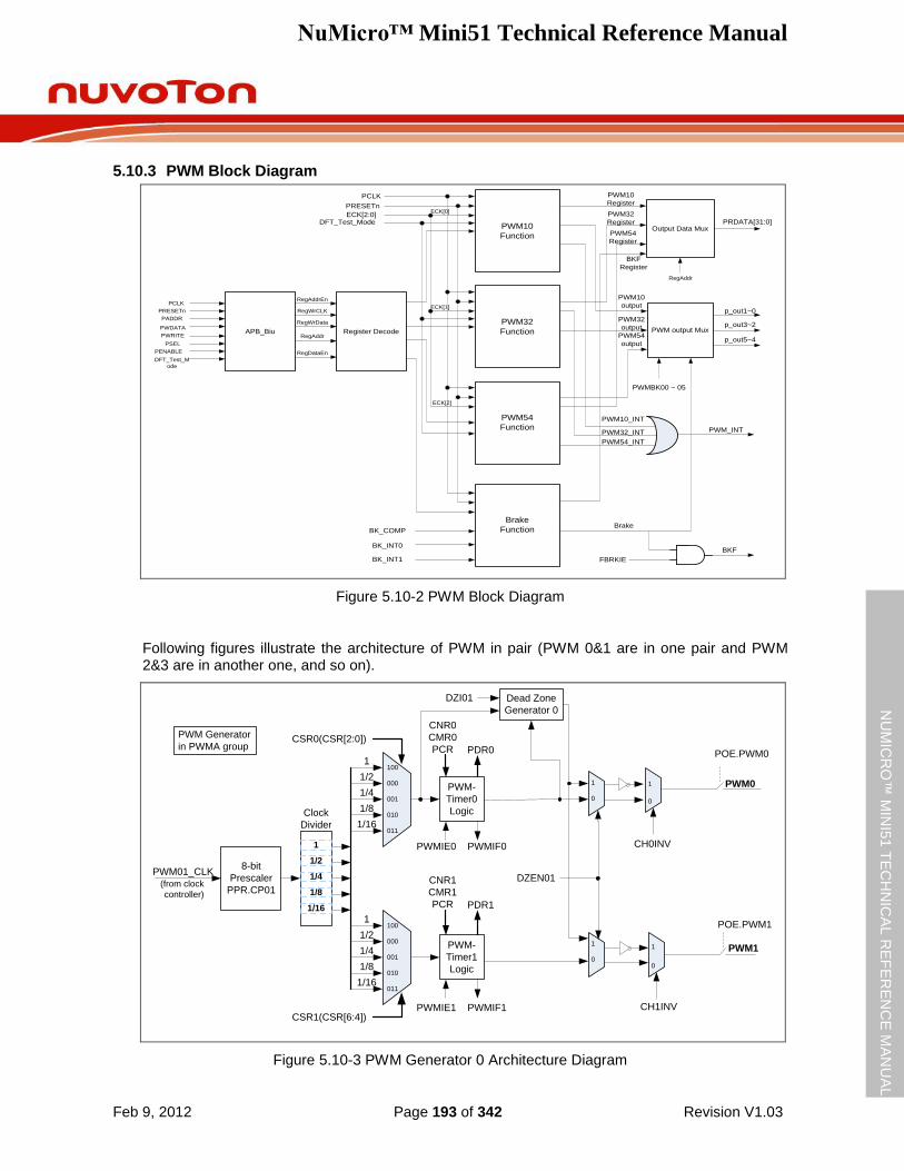
NuMicro™ Mini51 Technical Reference Manual
Feb 9, 2012 Page 193 of 342 Revision V1.03
NU
MIC
RO
™ M
INI5
1 T
EC
HN
ICA
L R
EF
ER
EN
CE
MA
NU
AL
5.10.3 PWM Block Diagram
APB_Biu
PWM10
Function
PWM32
Function
PWM54
Function
Brake
FunctionBK_COMP
BK_INT0
BK_INT1
Output Data Mux
Register Decode
PRDATA[31:0]
PWM output Mux
PWM10
Register
PWM32
Register
PWM54
Register
PWM10
output
PWM32
output
PWM54
output
p_out1~0
p_out3~2
p_out5~4
PWMBK00 ~ 05
PWM_INT
PWM10_INT
PWM32_INT
PWM54_INT
FBRKIE
BKF
BKF
Register
PCLK
PRESETn
ECK[2:0]ECK[0]
ECK[1]
ECK[2]
DFT_Test_Mode
PCLK
PRESETn
PADDR
PWDATA
PWRITE
PSEL
PENABLE
DFT_Test_M
ode
RegAddrEn
RegWrCLK
RegWrData
RegAddr
RegDataEn
Brake
RegAddr
Figure 5.10-2 PWM Block Diagram
Following figures illustrate the architecture of PWM in pair (PWM 0&1 are in one pair and PWM 2&3 are in another one, and so on).
CSR1(CSR[6:4])
100
000
1
1/2
1/4
1/8
1/16
001
010
011
100
000
1
1/2
1/4
1/8
1/16
001
010
011
CSR0(CSR[2:0])
8-bit
Prescaler
PPR.CP01
PWM-
Timer0
Logic
CNR0
CMR0
PCR
PWM-
Timer1
Logic
Dead Zone
Generator 0
DZI01
DZEN01
CH1INV
PWMIE0 PWMIF0
PWMIE1 PWMIF1
CNR1
CMR1
PCR
PWM01_CLK
1
1/2
1/4
1/8
1/16
Clock
Divider
PWM0
PWM1
POE.PWM0
POE.PWM1
(from clock
controller)
PDR0
PDR1
1
0
PWM Generator
in PWMA group
1
0
1
0
1
0
CH0INV
Figure 5.10-3 PWM Generator 0 Architecture Diagram
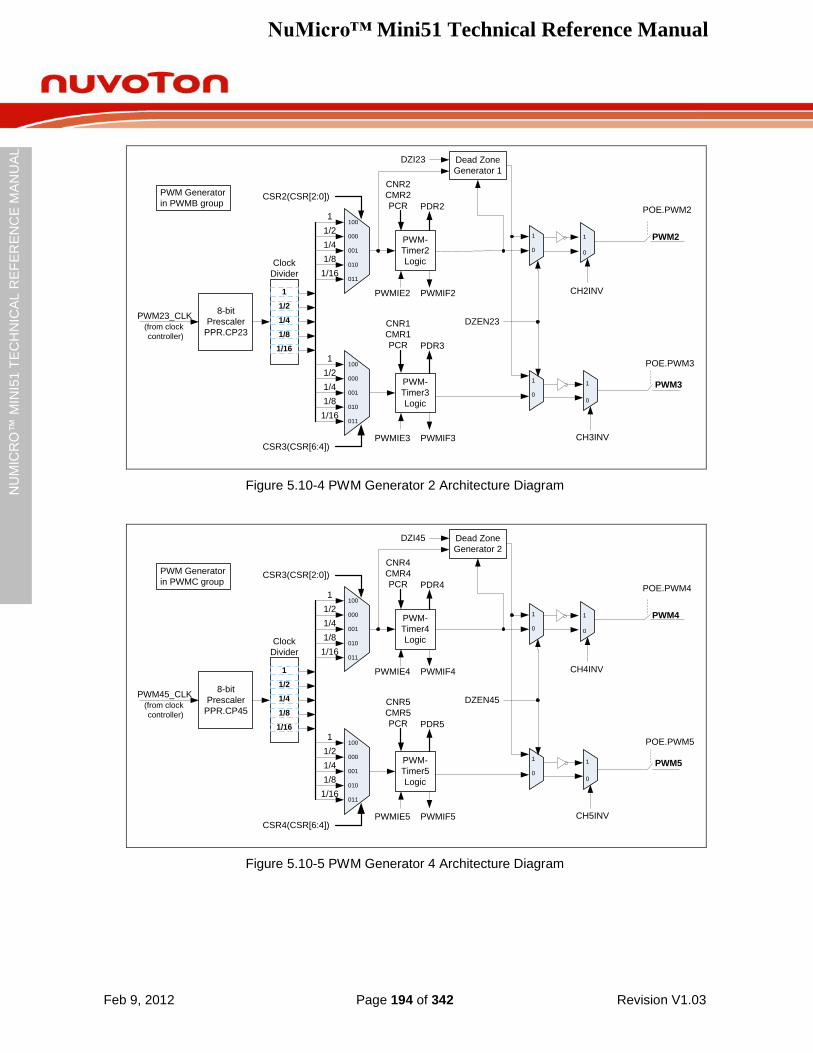
NuMicro™ Mini51 Technical Reference Manual
Feb 9, 2012 Page 194 of 342 Revision V1.03
NU
MIC
RO
™ M
INI5
1 T
EC
HN
ICA
L R
EF
ER
EN
CE
MA
NU
AL
CSR3(CSR[6:4])
100
000
1
1/2
1/4
1/8
1/16
001
010
011
100
000
1
1/2
1/4
1/8
1/16
001
010
011
CSR2(CSR[2:0])
8-bit
Prescaler
PPR.CP23
PWM-
Timer2
Logic
CNR2
CMR2
PCR
PWM-
Timer3
Logic
Dead Zone
Generator 1
DZI23
DZEN23
CH3INV
PWMIE2 PWMIF2
PWMIE3 PWMIF3
CNR1
CMR1
PCR
PWM23_CLK
1
1/2
1/4
1/8
1/16
Clock
Divider
PWM2
PWM3
POE.PWM2
POE.PWM3
(from clock
controller)
PDR2
PDR3
1
0
PWM Generator
in PWMB group
1
0
1
0
1
0
CH2INV
Figure 5.10-4 PWM Generator 2 Architecture Diagram
CSR4(CSR[6:4])
100
000
1
1/2
1/4
1/8
1/16
001
010
011
100
000
1
1/2
1/4
1/8
1/16
001
010
011
CSR3(CSR[2:0])
8-bit
Prescaler
PPR.CP45
PWM-
Timer4
Logic
CNR4
CMR4
PCR
PWM-
Timer5
Logic
Dead Zone
Generator 2
DZI45
DZEN45
CH5INV
PWMIE4 PWMIF4
PWMIE5 PWMIF5
CNR5
CMR5
PCR
PWM45_CLK
1
1/2
1/4
1/8
1/16
Clock
Divider
PWM4
PWM5
POE.PWM4
POE.PWM5
(from clock
controller)
PDR4
PDR5
1
0
PWM Generator
in PWMC group
1
0
1
0
1
0
CH4INV
Figure 5.10-5 PWM Generator 4 Architecture Diagram
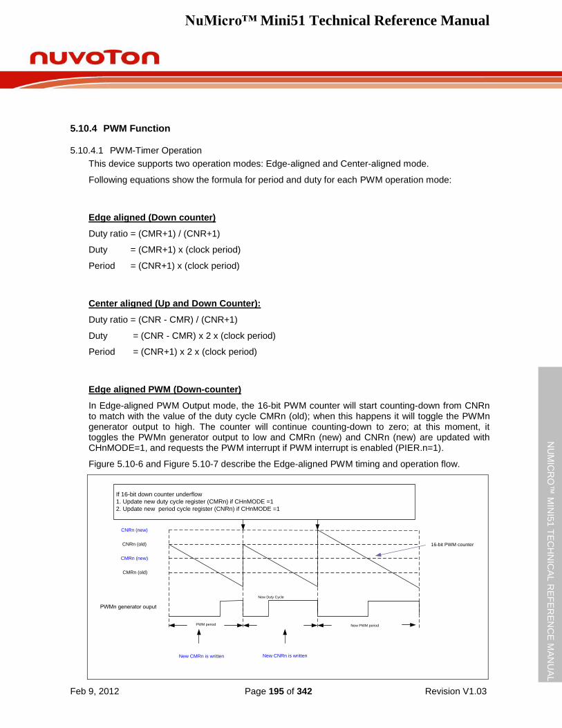
NuMicro™ Mini51 Technical Reference Manual
Feb 9, 2012 Page 195 of 342 Revision V1.03
NU
MIC
RO
™ M
INI5
1 T
EC
HN
ICA
L R
EF
ER
EN
CE
MA
NU
AL
5.10.4 PWM Function
5.10.4.1 PWM-Timer Operation
This device supports two operation modes: Edge-aligned and Center-aligned mode.
Following equations show the formula for period and duty for each PWM operation mode:
Edge aligned (Down counter)
Duty ratio = (CMR+1) / (CNR+1)
Duty = (CMR+1) x (clock period)
Period = (CNR+1) x (clock period)
Center aligned (Up and Down Counter):
Duty ratio = (CNR - CMR) / (CNR+1)
Duty = (CNR - CMR) x 2 x (clock period)
Period = (CNR+1) x 2 x (clock period)
Edge aligned PWM (Down-counter)
In Edge-aligned PWM Output mode, the 16-bit PWM counter will start counting-down from CNRn to match with the value of the duty cycle CMRn (old); when this happens it will toggle the PWMn generator output to high. The counter will continue counting-down to zero; at this moment, it toggles the PWMn generator output to low and CMRn (new) and CNRn (new) are updated with CHnMODE=1, and requests the PWM interrupt if PWM interrupt is enabled (PIER.n=1).
Figure 5.10-6 and Figure 5.10-7 describe the Edge-aligned PWM timing and operation flow.
CNRn (new)
CMRn (old)
CNRn (old)
CMRn (new)
New Duty Cycle
PWM period New PWM period
New CMRn is written New CNRn is written
If 16-bit down counter underflow
1. Update new duty cycle register (CMRn) if CHnMODE =1
2. Update new period cycle register (CNRn) if CHnMODE =1
PWMn generator ouput
16-bit PWM counter
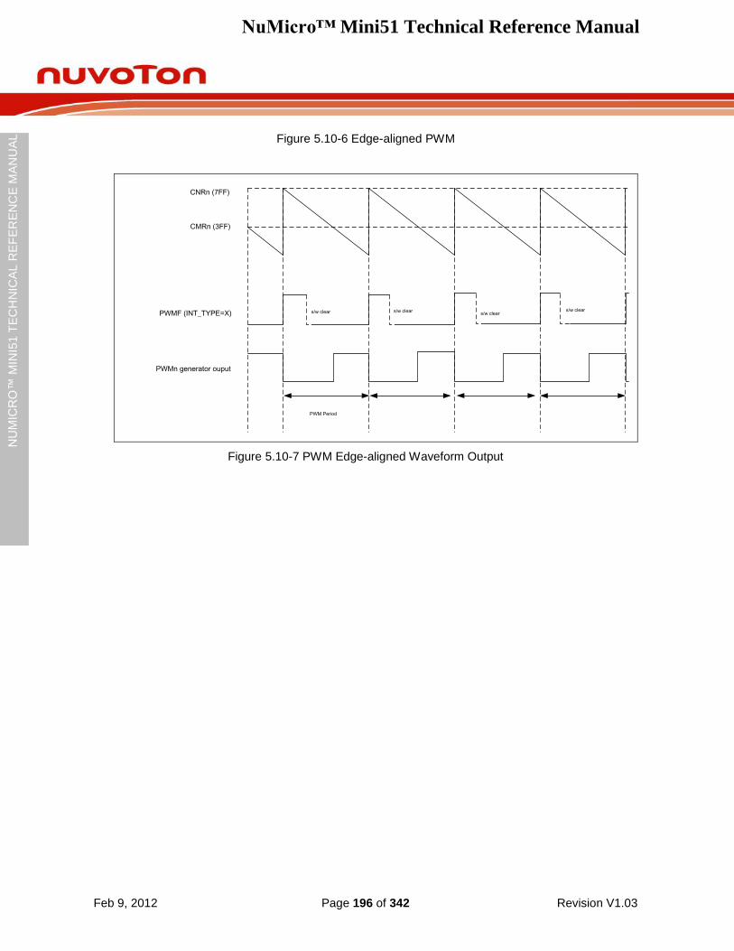
NuMicro™ Mini51 Technical Reference Manual
Feb 9, 2012 Page 196 of 342 Revision V1.03
NU
MIC
RO
™ M
INI5
1 T
EC
HN
ICA
L R
EF
ER
EN
CE
MA
NU
AL
Figure 5.10-6 Edge-aligned PWM
CNRn (7FF)
CMRn (3FF)
PWMn generator ouput
PWM Period
PWMF (INT_TYPE=X) s/w clears/w clear
s/w clears/w clear
Figure 5.10-7 PWM Edge-aligned Waveform Output
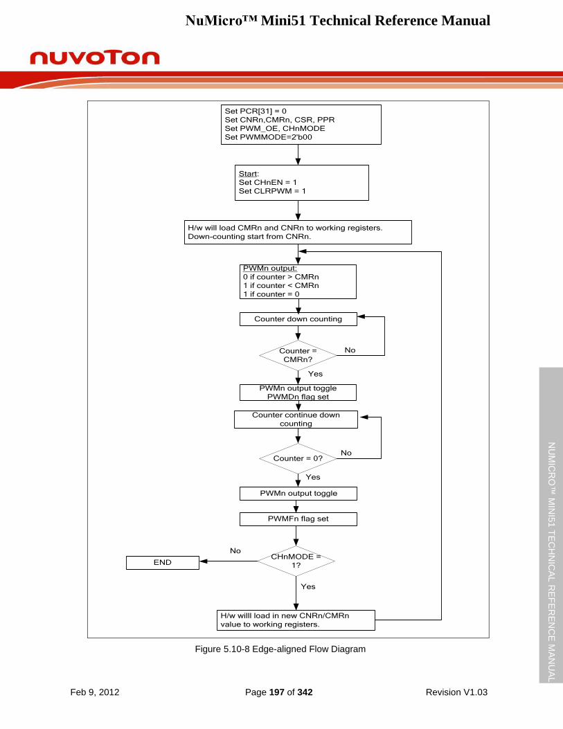
NuMicro™ Mini51 Technical Reference Manual
Feb 9, 2012 Page 197 of 342 Revision V1.03
NU
MIC
RO
™ M
INI5
1 T
EC
HN
ICA
L R
EF
ER
EN
CE
MA
NU
AL
Set PCR[31] = 0
Set CNRn,CMRn, CSR, PPR
Set PWM_OE, CHnMODE
Set PWMMODE=2'b00
Start:
Set CHnEN = 1
Set CLRPWM = 1
H/w will load CMRn and CNRn to working registers.
Down-counting start from CNRn.
PWMn output:
0 if counter > CMRn
1 if counter < CMRn
1 if counter = 0
Counter down counting
Counter =
CMRn?
PWMn output toggle
PWMDn flag set
Counter continue down
counting
Counter = 0?
PWMn output toggle
PWMFn flag set
CHnMODE =
1?
H/w willl load in new CNRn/CMRn
value to working registers.
No
No
No
Yes
END
Yes
Yes
Figure 5.10-8 Edge-aligned Flow Diagram
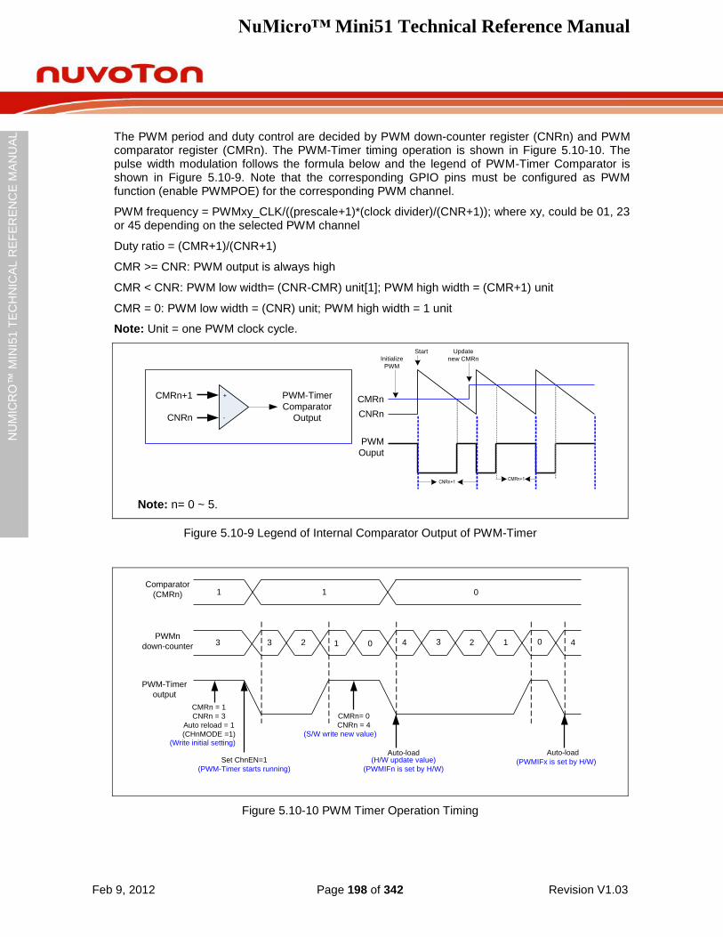
NuMicro™ Mini51 Technical Reference Manual
Feb 9, 2012 Page 198 of 342 Revision V1.03
NU
MIC
RO
™ M
INI5
1 T
EC
HN
ICA
L R
EF
ER
EN
CE
MA
NU
AL
The PWM period and duty control are decided by PWM down-counter register (CNRn) and PWM comparator register (CMRn). The PWM-Timer timing operation is shown in Figure 5.10-10. The pulse width modulation follows the formula below and the legend of PWM-Timer Comparator is shown in Figure 5.10-9. Note that the corresponding GPIO pins must be configured as PWM function (enable PWMPOE) for the corresponding PWM channel.
PWM frequency = PWMxy_CLK/((prescale+1)*(clock divider)/(CNR+1)); where xy, could be 01, 23 or 45 depending on the selected PWM channel
Duty ratio = (CMR+1)/(CNR+1)
CMR >= CNR: PWM output is always high
CMR < CNR: PWM low width= (CNR-CMR) unit[1]; PWM high width = (CMR+1) unit
CMR = 0: PWM low width = (CNR) unit; PWM high width = 1 unit
Note: Unit = one PWM clock cycle.
+
-
CMRn+1
CNRn
PWM-Timer
Comparator
Output CNRn
CMRn
Update
new CMRn
Start
Initialize
PWM
PWM
Ouput
CMRn+1CNRn+1
Note: n= 0 ~ 5.
Figure 5.10-9 Legend of Internal Comparator Output of PWM-Timer
Comparator
(CMRn) 1 0
PWMn
down-counter 3 3 2 1 0 4 3 2 1 0 4
PWM-Timer
output
1
CMRn = 1
CNRn = 3
Auto reload = 1
(CHnMODE =1)
Set ChnEN=1
(PWM-Timer starts running)
CMRn= 0
CNRn = 4
Auto-load
(S/W write new value)
Auto-load
(Write initial setting)
(H/W update value)
(PWMIFn is set by H/W)(PWMIFx is set by H/W)
Figure 5.10-10 PWM Timer Operation Timing
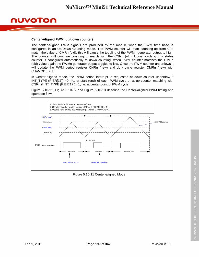
NuMicro™ Mini51 Technical Reference Manual
Feb 9, 2012 Page 199 of 342 Revision V1.03
NU
MIC
RO
™ M
INI5
1 T
EC
HN
ICA
L R
EF
ER
EN
CE
MA
NU
AL
Center-Aligned PWM (up/down counter)
The center-aligned PWM signals are produced by the module when the PWM time base is configured in an Up/Down Counting mode. The PWM counter will start counting-up from 0 to match the value of CMRn (old); this will cause the toggling of the PWMn generator output to high. The counter will continue counting to match with the CNRn (old). Upon reaching this states counter is configured automatically to down counting, when PWM counter matches the CMRn (old) value again the PWMn generator output toggles to low. Once the PWM counter underflows it will update the PWM period register CNRn (new) and duty cycle register CMRn (new) with CHnMODE = 1.
In Center-aligned mode, the PWM period interrupt is requested at down-counter underflow if INT_TYPE (PIER[17]) =0, i.e. at start (end) of each PWM cycle or at up-counter matching with CNRn if INT_TYPE (PIER[17]) =1, i.e. at center point of PWM cycle.
Figure 5.10-11, Figure 5.10-12 and Figure 5.10-13 describe the Center-aligned PWM timing and operation flow.
CNRn (new)
CMRn (old)
CNRn (old)
CMRn (new)
New Duty Cycle
PWM period New PWM period
New CMRn is written New CNRn is written
If 16-bit PWM up/down counter underflows
1. Update new duty cycle register (CMRn) if CHnMODE = 1
2. Update new period cycle register (CNRn) if CHnMODE = 1
PWM period
PWMn generator ouput
16-bit PWM counter
Figure 5.10-11 Center-aligned Mode
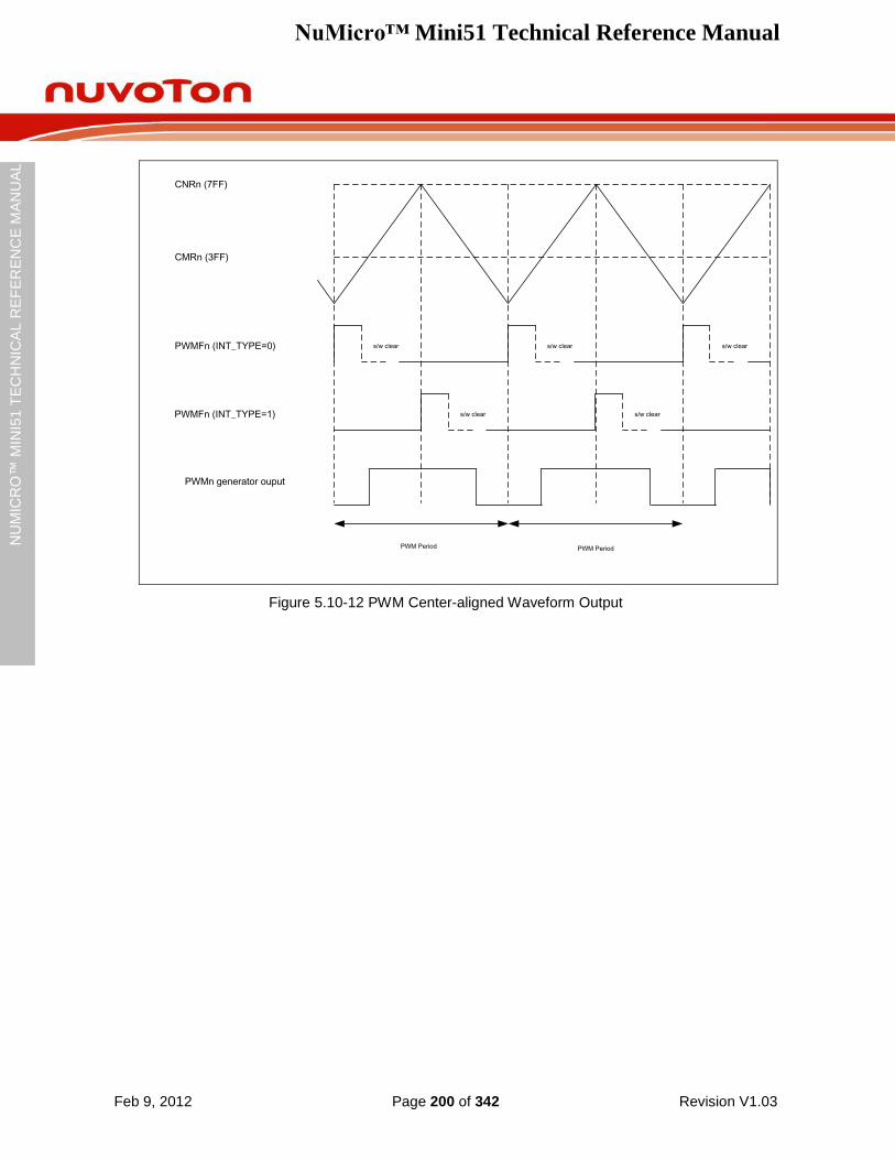
NuMicro™ Mini51 Technical Reference Manual
Feb 9, 2012 Page 200 of 342 Revision V1.03
NU
MIC
RO
™ M
INI5
1 T
EC
HN
ICA
L R
EF
ER
EN
CE
MA
NU
AL
CNRn (7FF)
CMRn (3FF)
PWM Period
PWMFn (INT_TYPE=0) s/w clear s/w clears/w clear
PWMFn (INT_TYPE=1) s/w clear s/w clear
PWM Period
PWMn generator ouput
Figure 5.10-12 PWM Center-aligned Waveform Output
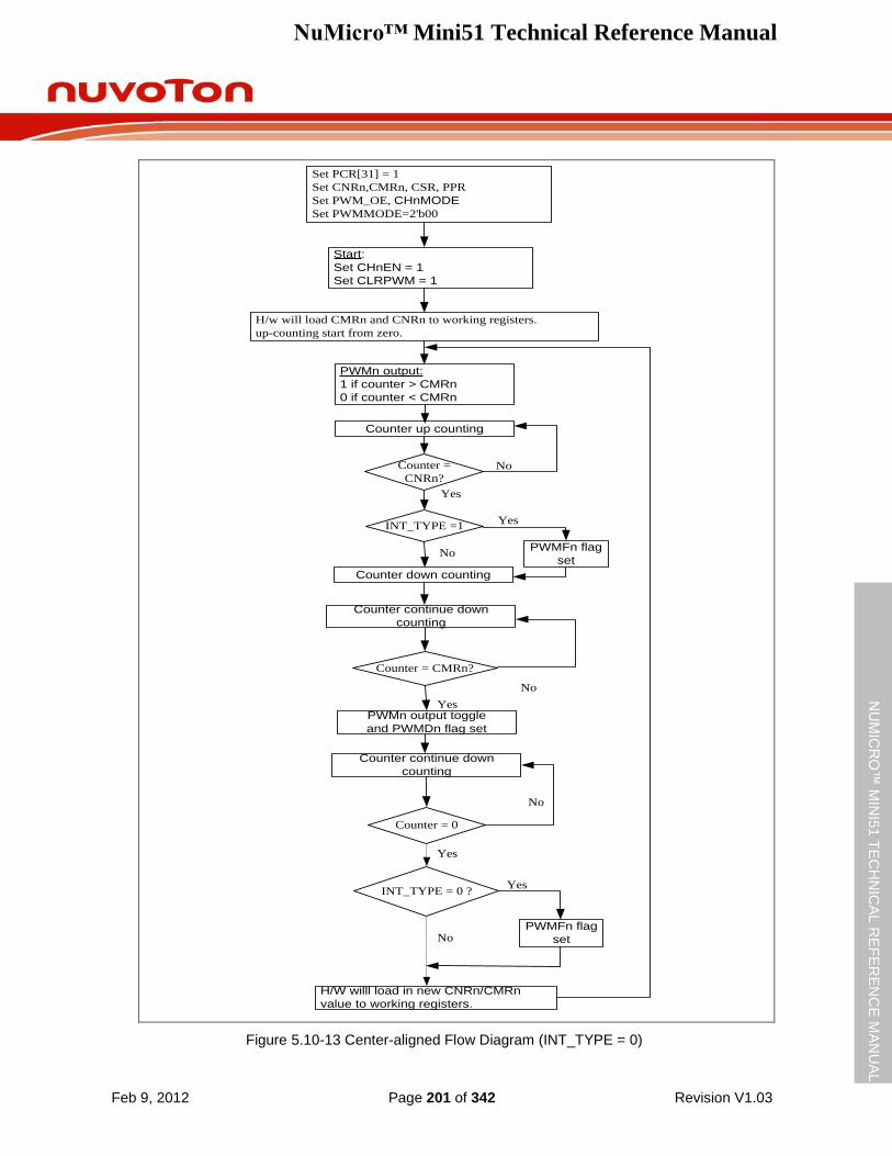
NuMicro™ Mini51 Technical Reference Manual
Feb 9, 2012 Page 201 of 342 Revision V1.03
NU
MIC
RO
™ M
INI5
1 T
EC
HN
ICA
L R
EF
ER
EN
CE
MA
NU
AL
Set PCR[31] = 1
Set CNRn,CMRn, CSR, PPR
Set PWM_OE, CHnMODE
Set PWMMODE=2'b00
Start:
Set CHnEN = 1
Set CLRPWM = 1
H/w will load CMRn and CNRn to working registers.
up-counting start from zero.
PWMn output:
1 if counter > CMRn
0 if counter < CMRn
Counter up counting
Counter =
CNRn?
Counter down counting
Counter continue down
counting
Counter = CMRn?
PWMn output toggle
and PWMDn flag set
H/W willl load in new CNRn/CMRn
value to working registers.
No
No
Yes
Yes
INT_TYPE =1
PWMFn flag
set
Yes
No
Counter = 0
Counter continue down
counting
No
INT_TYPE = 0 ?
PWMFn flag
set
Yes
No
Yes
Figure 5.10-13 Center-aligned Flow Diagram (INT_TYPE = 0)
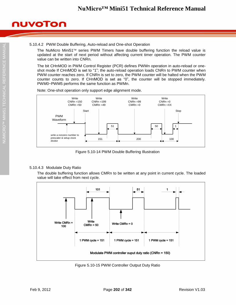
NuMicro™ Mini51 Technical Reference Manual
Feb 9, 2012 Page 202 of 342 Revision V1.03
NU
MIC
RO
™ M
INI5
1 T
EC
HN
ICA
L R
EF
ER
EN
CE
MA
NU
AL
5.10.4.2 PWM Double Buffering, Auto-reload and One-shot Operation
The NuMicro Mini51 series PWM Timers have double buffering function the reload value is updated at the start of next period without affecting current timer operation. The PWM counter value can be written into CNRn.
The bit CHnMOD in PWM Control Register (PCR) defines PWMn operation in auto-reload or one-shot mode If CHnMOD is set to “1”; the auto-reload operation loads CNRn to PWM counter when PWM counter reaches zero. If CNRn is set to zero, the PWM counter will be halted when the PWM counter counts to zero. If CHnMOD is set as “0”, the counter will be stopped immediately. PWM0~PWM5 performs the same function as PWMn.
Note: One-shot operation only support edge alignment mode.
PWM
Waveform
write a nonzero number to
prescaler & setup clock
dividor
Start
Write
CNRn =150
CMRn =50
151
51
200
50
Write
CNRn =199
CMRn =49
Write
CNRn =99
CMRn =0
100
1
Write
CNRn =0
CMRn =XX
Stop
Figure 5.10-14 PWM Double Buffering Illustration
5.10.4.3 Modulate Duty Ratio
The double buffering function allows CMRn to be written at any point in current cycle. The loaded value will take effect from next cycle.
Modulate PWM controller ouput duty ratio (CNRn = 150)
Write CMRn =
100
Write
CMRn = 50 Write CMRn = 0
1 PWM cycle = 151 1 PWM cycle = 151 1 PWM cycle = 151
101 51 1
Figure 5.10-15 PWM Controller Output Duty Ratio
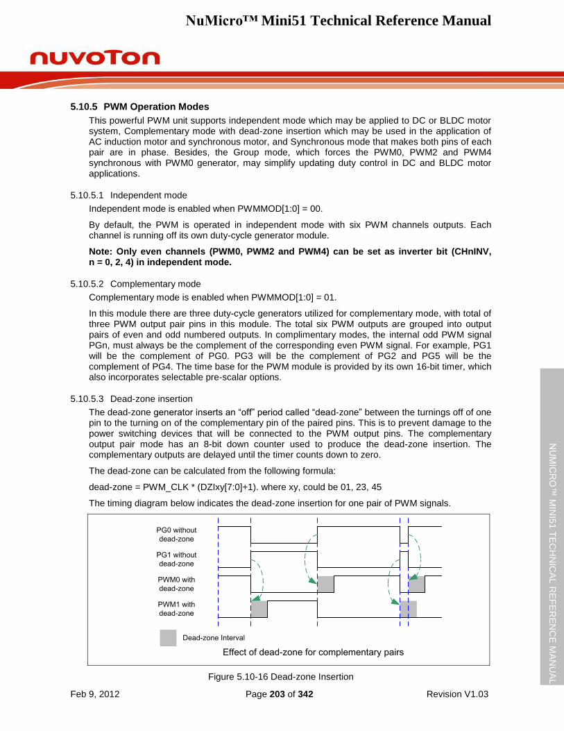
NuMicro™ Mini51 Technical Reference Manual
Feb 9, 2012 Page 203 of 342 Revision V1.03
NU
MIC
RO
™ M
INI5
1 T
EC
HN
ICA
L R
EF
ER
EN
CE
MA
NU
AL
5.10.5 PWM Operation Modes
This powerful PWM unit supports independent mode which may be applied to DC or BLDC motor system, Complementary mode with dead-zone insertion which may be used in the application of AC induction motor and synchronous motor, and Synchronous mode that makes both pins of each pair are in phase. Besides, the Group mode, which forces the PWM0, PWM2 and PWM4 synchronous with PWM0 generator, may simplify updating duty control in DC and BLDC motor applications.
5.10.5.1 Independent mode
Independent mode is enabled when PWMMOD[1:0] = 00.
By default, the PWM is operated in independent mode with six PWM channels outputs. Each channel is running off its own duty-cycle generator module.
Note: Only even channels (PWM0, PWM2 and PWM4) can be set as inverter bit (CHnINV, n = 0, 2, 4) in independent mode.
5.10.5.2 Complementary mode
Complementary mode is enabled when PWMMOD[1:0] = 01.
In this module there are three duty-cycle generators utilized for complementary mode, with total of three PWM output pair pins in this module. The total six PWM outputs are grouped into output pairs of even and odd numbered outputs. In complimentary modes, the internal odd PWM signal PGn, must always be the complement of the corresponding even PWM signal. For example, PG1 will be the complement of PG0. PG3 will be the complement of PG2 and PG5 will be the complement of PG4. The time base for the PWM module is provided by its own 16-bit timer, which also incorporates selectable pre-scalar options.
5.10.5.3 Dead-zone insertion
The dead-zone generator inserts an “off” period called “dead-zone” between the turnings off of one pin to the turning on of the complementary pin of the paired pins. This is to prevent damage to the power switching devices that will be connected to the PWM output pins. The complementary output pair mode has an 8-bit down counter used to produce the dead-zone insertion. The complementary outputs are delayed until the timer counts down to zero.
The dead-zone can be calculated from the following formula:
dead-zone = PWM_CLK * (DZIxy[7:0]+1). where xy, could be 01, 23, 45
The timing diagram below indicates the dead-zone insertion for one pair of PWM signals.
PG0 without
dead-zone
PG1 without
dead-zone
PWM0 with
dead-zone
PWM1 with
dead-zone
Dead-zone Interval
Effect of dead-zone for complementary pairs
Figure 5.10-16 Dead-zone Insertion
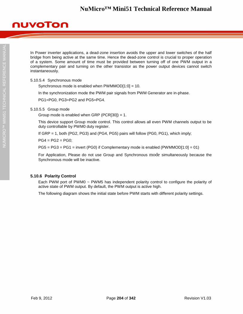
NuMicro™ Mini51 Technical Reference Manual
Feb 9, 2012 Page 204 of 342 Revision V1.03
NU
MIC
RO
™ M
INI5
1 T
EC
HN
ICA
L R
EF
ER
EN
CE
MA
NU
AL
In Power inverter applications, a dead-zone insertion avoids the upper and lower switches of the half bridge from being active at the same time. Hence the dead-zone control is crucial to proper operation of a system. Some amount of time must be provided between turning off of one PWM output in a complementary pair and turning on the other transistor as the power output devices cannot switch instantaneously.
5.10.5.4 Synchronous mode
Synchronous mode is enabled when PWMMOD[1:0] = 10.
In the synchronization mode the PWM pair signals from PWM Generator are in-phase.
PG1=PG0, PG3=PG2 and PG5=PG4.
5.10.5.5 Group mode
Group mode is enabled when GRP (PCR[30]) = 1.
This device support Group mode control. This control allows all even PWM channels output to be duty controllable by PWM0 duty register.
If GRP = 1, both (PG2, PG3) and (PG4, PG5) pairs will follow (PG0, PG1), which imply;
PG4 = PG2 = PG0;
PG5 = PG3 = PG1 = invert (PG0) if Complementary mode is enabled (PWMMOD[1:0] = 01)
For Application, Please do not use Group and Synchronous mode simultaneously because the
Synchronous mode will be inactive.
5.10.6 Polarity Control
Each PWM port of PWM0 ~ PWM5 has independent polarity control to configure the polarity of active state of PWM output. By default, the PWM output is active high.
The following diagram shows the initial state before PWM starts with different polarity settings.
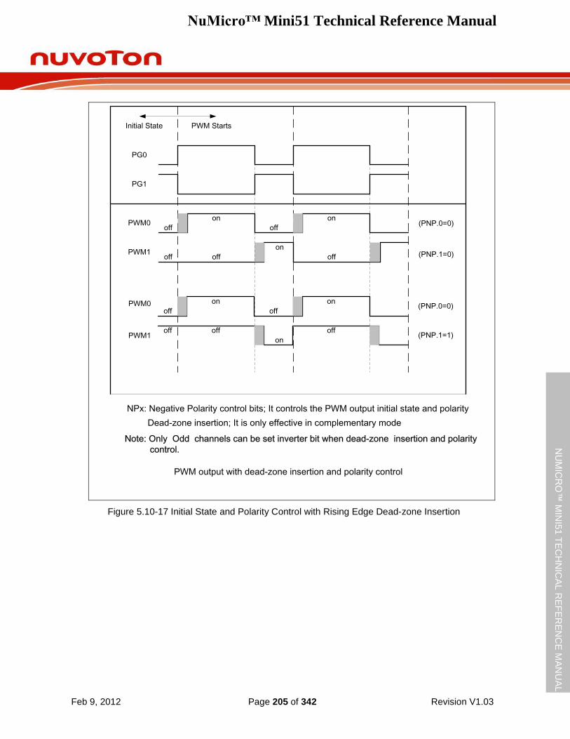
NuMicro™ Mini51 Technical Reference Manual
Feb 9, 2012 Page 205 of 342 Revision V1.03
NU
MIC
RO
™ M
INI5
1 T
EC
HN
ICA
L R
EF
ER
EN
CE
MA
NU
AL
PG0
PG1
PWM0
PWM1
off
on on
off
off
off
on
off
(PNP.0=0)
(PNP.1=0)
Dead-zone insertion; It is only effective in complementary mode
NPx: Negative Polarity control bits; It controls the PWM output initial state and polarity
PWM0
PWM1
(PNP.0=0)
(PNP.1=1)
Initial State PWM Starts
off
on on
off
off off
on
off
PWM output with dead-zone insertion and polarity control
Note: Only Odd channels can be set inverter bit when dead-zone insertion and polarity
control.
Figure 5.10-17 Initial State and Polarity Control with Rising Edge Dead-zone Insertion
NuMicro™ Mini51 Technical Reference Manual
Feb 9, 2012 Page 206 of 342 Revision V1.03
NU
MIC
RO
™ M
INI5
1 T
EC
HN
ICA
L R
EF
ER
EN
CE
MA
NU
AL
5.10.7 PWM for Motor Control Interrupt Architecture
There are 4 interrupt sources for a PWM unit, which are PWM period flag (PWMPIF), PWM duty interrupt(PWMDIF), Brake0 flag (BKF0) and Brake1 flag (BKF1). The bit BRKIE (PIER[16]) controls the brake interrupt enable; the bit PWMPIEn (PIER[0] ~ PIER[5]) controls the PWM periodic interrupt enable; and the bit PWMDIEn (PIER[8] ~ PIER[13]) controls the PWM duty interrupt enable. Note that all the interrupt flags are set by hardware and must be cleared by software.
Figure 5.10-18 demonstrates the architecture of Motor Control PWM interrupts.
BKF0
BKF1
PWMPIFn
Brake_INT
PWM_ INT
BRKIE
PWMDIFn
PWMPIEn
PWMDIEn
Figure 5.10-18 Motor Control PWM Architecture
5.10.8 PWM Brake Function
This device supports two external brake pins: BKP0 and BKP1 pins. The Brake function is controlled by the contents of the PFBCON registers.
Since the both brake conditions being asserted will automatically rise the BKF flag, user program can poll these brake flag bits or enable PWM‟s brake interrupt to determine which condition causes a brake to occur.
Note: When a brake happens, the PWM0 ~ PWM5 enable bits will be disabled by hardware.
User program must write the PWM enable bits again to release PWM Brake state.
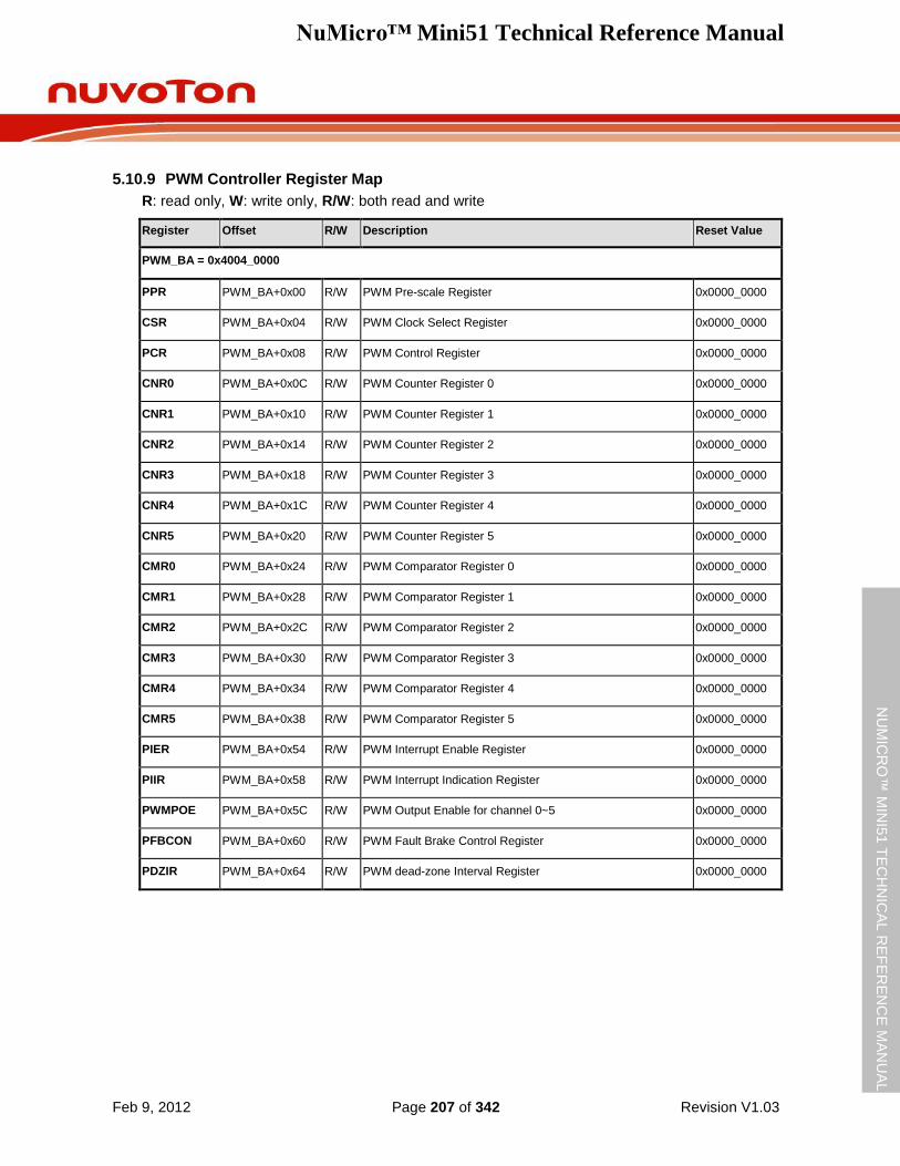
NuMicro™ Mini51 Technical Reference Manual
Feb 9, 2012 Page 207 of 342 Revision V1.03
NU
MIC
RO
™ M
INI5
1 T
EC
HN
ICA
L R
EF
ER
EN
CE
MA
NU
AL
5.10.9 PWM Controller Register Map
R: read only, W: write only, R/W: both read and write
Register Offset R/W Description Reset Value
PWM_BA = 0x4004_0000
PPR PWM_BA+0x00 R/W PWM Pre-scale Register 0x0000_0000
CSR PWM_BA+0x04 R/W PWM Clock Select Register 0x0000_0000
PCR PWM_BA+0x08 R/W PWM Control Register 0x0000_0000
CNR0 PWM_BA+0x0C R/W PWM Counter Register 0 0x0000_0000
CNR1 PWM_BA+0x10 R/W PWM Counter Register 1 0x0000_0000
CNR2 PWM_BA+0x14 R/W PWM Counter Register 2 0x0000_0000
CNR3 PWM_BA+0x18 R/W PWM Counter Register 3 0x0000_0000
CNR4 PWM_BA+0x1C R/W PWM Counter Register 4 0x0000_0000
CNR5 PWM_BA+0x20 R/W PWM Counter Register 5 0x0000_0000
CMR0 PWM_BA+0x24 R/W PWM Comparator Register 0 0x0000_0000
CMR1 PWM_BA+0x28 R/W PWM Comparator Register 1 0x0000_0000
CMR2 PWM_BA+0x2C R/W PWM Comparator Register 2 0x0000_0000
CMR3 PWM_BA+0x30 R/W PWM Comparator Register 3 0x0000_0000
CMR4 PWM_BA+0x34 R/W PWM Comparator Register 4 0x0000_0000
CMR5 PWM_BA+0x38 R/W PWM Comparator Register 5 0x0000_0000
PIER PWM_BA+0x54 R/W PWM Interrupt Enable Register 0x0000_0000
PIIR PWM_BA+0x58 R/W PWM Interrupt Indication Register 0x0000_0000
PWMPOE PWM_BA+0x5C R/W PWM Output Enable for channel 0~5 0x0000_0000
PFBCON PWM_BA+0x60 R/W PWM Fault Brake Control Register 0x0000_0000
PDZIR PWM_BA+0x64 R/W PWM dead-zone Interval Register 0x0000_0000
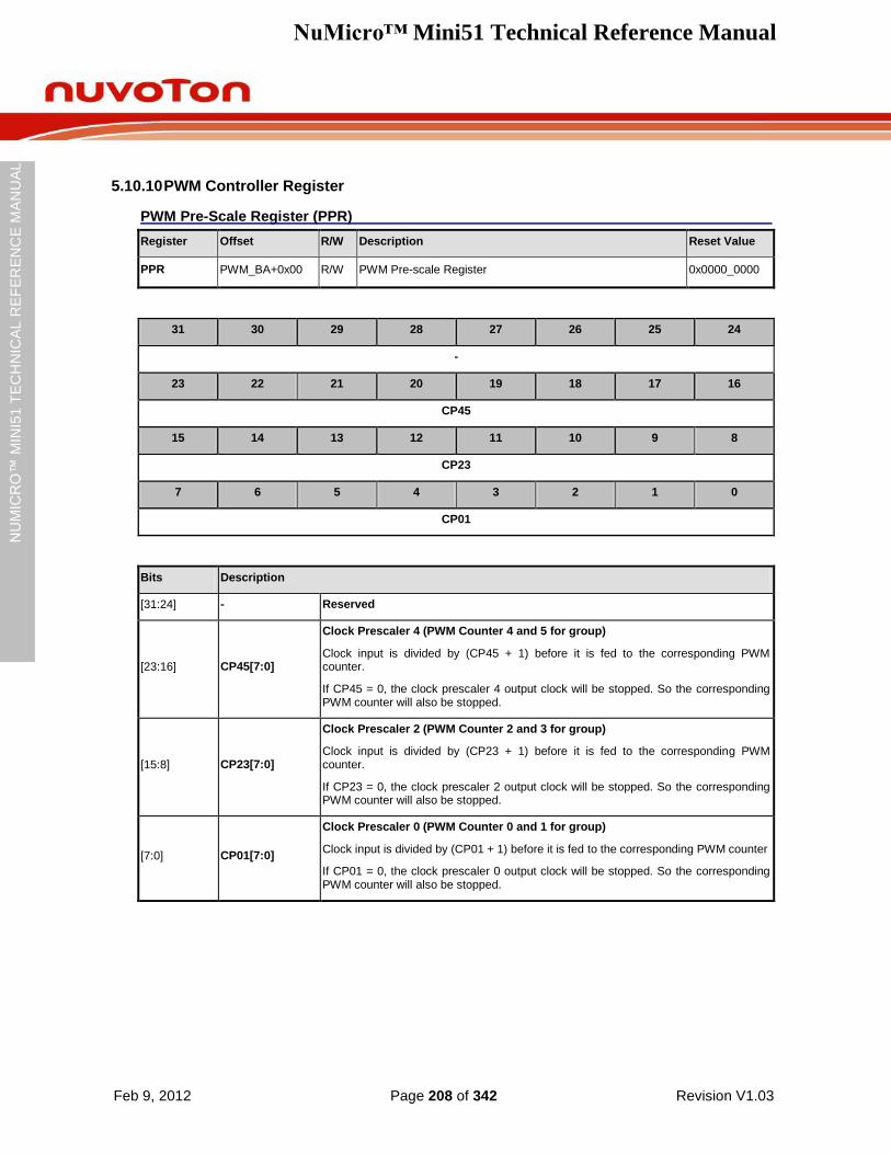
NuMicro™ Mini51 Technical Reference Manual
Feb 9, 2012 Page 208 of 342 Revision V1.03
NU
MIC
RO
™ M
INI5
1 T
EC
HN
ICA
L R
EF
ER
EN
CE
MA
NU
AL
5.10.10 PWM Controller Register
PWM Pre-Scale Register (PPR)
Register Offset R/W Description Reset Value
PPR PWM_BA+0x00 R/W PWM Pre-scale Register 0x0000_0000
31 30 29 28 27 26 25 24
-
23 22 21 20 19 18 17 16
CP45
15 14 13 12 11 10 9 8
CP23
7 6 5 4 3 2 1 0
CP01
Bits Description
[31:24] - Reserved
[23:16] CP45[7:0]
Clock Prescaler 4 (PWM Counter 4 and 5 for group)
Clock input is divided by (CP45 + 1) before it is fed to the corresponding PWM counter.
If CP45 = 0, the clock prescaler 4 output clock will be stopped. So the corresponding PWM counter will also be stopped.
[15:8] CP23[7:0]
Clock Prescaler 2 (PWM Counter 2 and 3 for group)
Clock input is divided by (CP23 + 1) before it is fed to the corresponding PWM counter.
If CP23 = 0, the clock prescaler 2 output clock will be stopped. So the corresponding PWM counter will also be stopped.
[7:0] CP01[7:0]
Clock Prescaler 0 (PWM Counter 0 and 1 for group)
Clock input is divided by (CP01 + 1) before it is fed to the corresponding PWM counter
If CP01 = 0, the clock prescaler 0 output clock will be stopped. So the corresponding PWM counter will also be stopped.
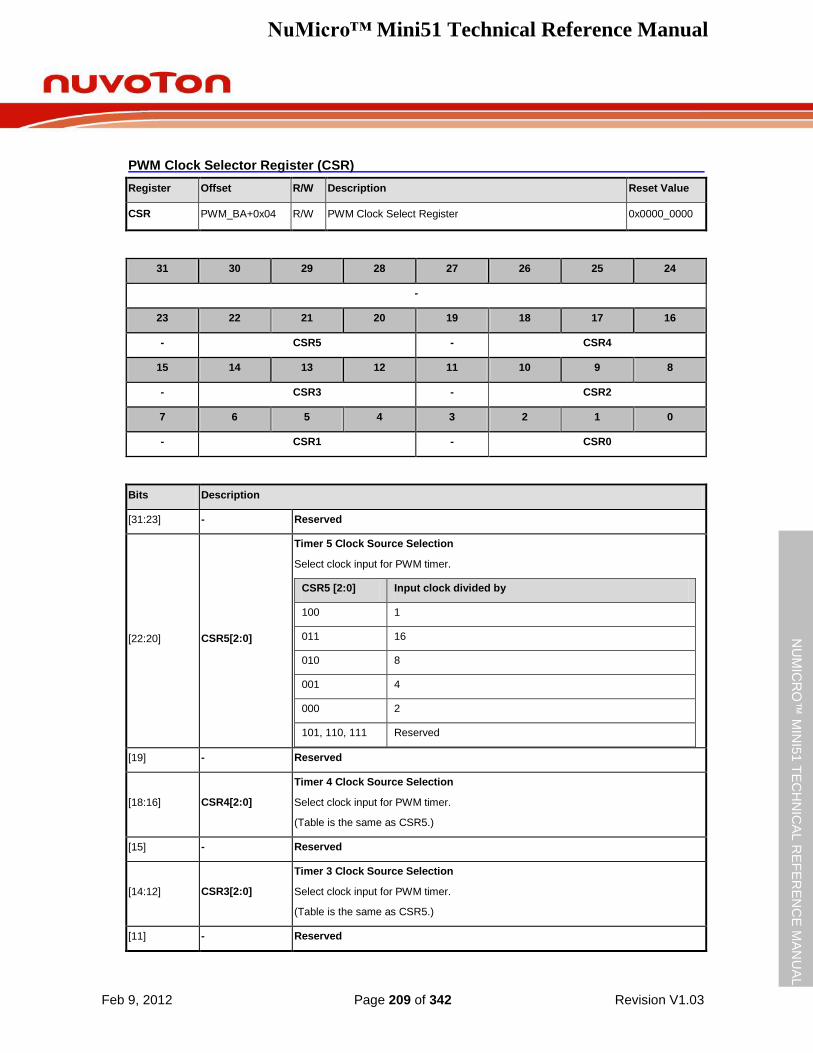
NuMicro™ Mini51 Technical Reference Manual
Feb 9, 2012 Page 209 of 342 Revision V1.03
NU
MIC
RO
™ M
INI5
1 T
EC
HN
ICA
L R
EF
ER
EN
CE
MA
NU
AL
PWM Clock Selector Register (CSR)
Register Offset R/W Description Reset Value
CSR PWM_BA+0x04 R/W PWM Clock Select Register 0x0000_0000
31 30 29 28 27 26 25 24
-
23 22 21 20 19 18 17 16
- CSR5 - CSR4
15 14 13 12 11 10 9 8
- CSR3 - CSR2
7 6 5 4 3 2 1 0
- CSR1 - CSR0
Bits Description
[31:23] - Reserved
[22:20] CSR5[2:0]
Timer 5 Clock Source Selection
Select clock input for PWM timer.
CSR5 [2:0] Input clock divided by
100 1
011 16
010 8
001 4
000 2
101, 110, 111 Reserved
[19] - Reserved
[18:16] CSR4[2:0]
Timer 4 Clock Source Selection
Select clock input for PWM timer.
(Table is the same as CSR5.)
[15] - Reserved
[14:12] CSR3[2:0]
Timer 3 Clock Source Selection
Select clock input for PWM timer.
(Table is the same as CSR5.)
[11] - Reserved
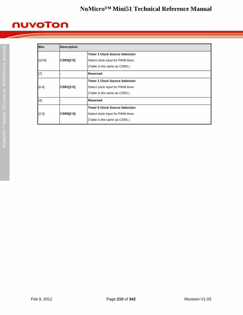
NuMicro™ Mini51 Technical Reference Manual
Feb 9, 2012 Page 210 of 342 Revision V1.03
NU
MIC
RO
™ M
INI5
1 T
EC
HN
ICA
L R
EF
ER
EN
CE
MA
NU
AL
Bits Description
[10:8] CSR2[2:0]
Timer 2 Clock Source Selection
Select clock input for PWM timer.
(Table is the same as CSR5.)
[7] - Reserved
[6:4] CSR1[2:0]
Timer 1 Clock Source Selection
Select clock input for PWM timer.
(Table is the same as CSR5.)
[3] - Reserved
[2:0] CSR0[2:0]
Timer 0 Clock Source Selection
Select clock input for PWM timer.
(Table is the same as CSR5.)
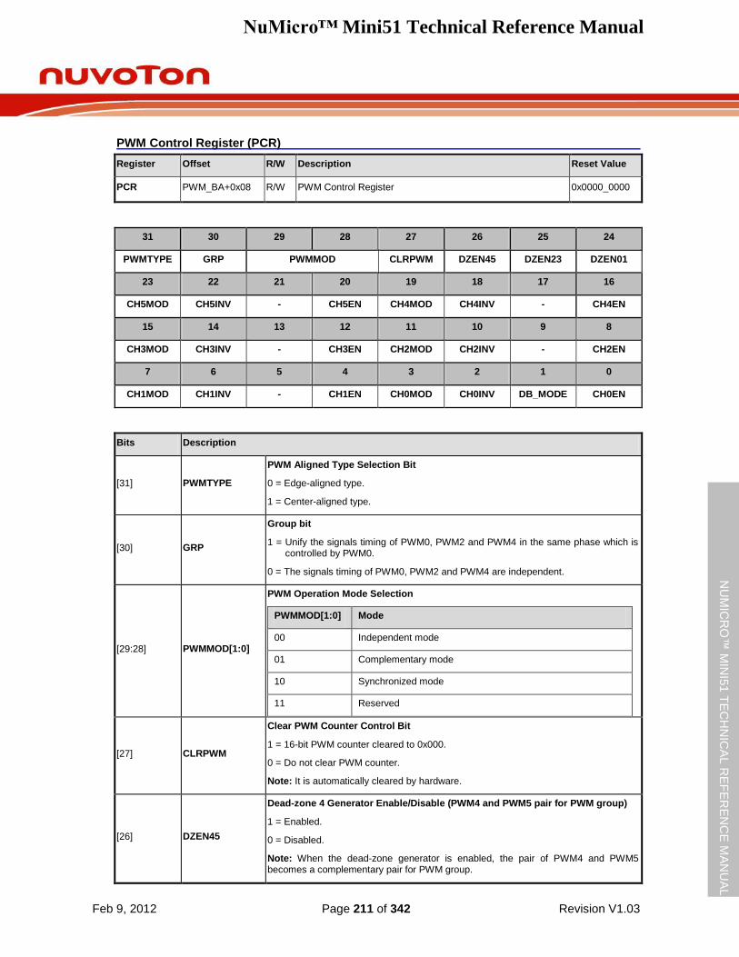
NuMicro™ Mini51 Technical Reference Manual
Feb 9, 2012 Page 211 of 342 Revision V1.03
NU
MIC
RO
™ M
INI5
1 T
EC
HN
ICA
L R
EF
ER
EN
CE
MA
NU
AL
PWM Control Register (PCR)
Register Offset R/W Description Reset Value
PCR PWM_BA+0x08 R/W PWM Control Register 0x0000_0000
31 30 29 28 27 26 25 24
PWMTYPE GRP PWMMOD CLRPWM DZEN45 DZEN23 DZEN01
23 22 21 20 19 18 17 16
CH5MOD CH5INV - CH5EN CH4MOD CH4INV - CH4EN
15 14 13 12 11 10 9 8
CH3MOD CH3INV - CH3EN CH2MOD CH2INV - CH2EN
7 6 5 4 3 2 1 0
CH1MOD CH1INV - CH1EN CH0MOD CH0INV DB_MODE CH0EN
Bits Description
[31] PWMTYPE
PWM Aligned Type Selection Bit
0 = Edge-aligned type.
1 = Center-aligned type.
[30] GRP
Group bit
1 = Unify the signals timing of PWM0, PWM2 and PWM4 in the same phase which is controlled by PWM0.
0 = The signals timing of PWM0, PWM2 and PWM4 are independent.
[29:28] PWMMOD[1:0]
PWM Operation Mode Selection
PWMMOD[1:0] Mode
00 Independent mode
01 Complementary mode
10 Synchronized mode
11 Reserved
[27] CLRPWM
Clear PWM Counter Control Bit
1 = 16-bit PWM counter cleared to 0x000.
0 = Do not clear PWM counter.
Note: It is automatically cleared by hardware.
[26] DZEN45
Dead-zone 4 Generator Enable/Disable (PWM4 and PWM5 pair for PWM group)
1 = Enabled.
0 = Disabled.
Note: When the dead-zone generator is enabled, the pair of PWM4 and PWM5 becomes a complementary pair for PWM group.
NuMicro™ Mini51 Technical Reference Manual
Feb 9, 2012 Page 212 of 342 Revision V1.03
NU
MIC
RO
™ M
INI5
1 T
EC
HN
ICA
L R
EF
ER
EN
CE
MA
NU
AL
Bits Description
[25] DZEN23
Dead-zone 2 Generator Enable/Disable (PWM2 and PWM3 pair for PWM group)
1 = Enabled.
0 = Disabled.
Note: When the dead-zone generator is enabled, the pair of PWM2 and PWM3 becomes a complementary pair for PWM group.
[24] DZEN01
Dead-zone 0 Generator Enable/Disable (PWM0 and PWM1 pair for PWM group)
1 = Enabled.
0 = Disabled.
Note: When the dead-zone generator is enabled, the pair of PWM0 and PWM1 becomes a complementary pair for PWM group.
[23] CH5MOD
PWM-Timer 5 Auto-reload/One-Shot Mode
1 = Auto-reload mode.
0 = One-shot mode.
Note: If there is a rising transition at this bit, it will cause CNR5 and CMR5 cleared.
[22] CH5INV
PWM-Timer 5 Output Inverter ON/OFF
1 = Inverter ON.
0 = Inverter OFF.
Note: Only even channels (PWM0, PWM2 and PWM4) can be set as inverter bit in independent mode
[21] - Reserved
[20] CH5EN
PWM-Timer 5 Enable/Disable Start Run
1 = Corresponding PWM-timer start run Enabled.
0 = Corresponding PWM-timer running Stopped.
[19] CH4MOD
PWM-Timer 4 Auto-reload/One-Shot Mode
1 = Auto-reload mode.
0 = One-shot mode.
Note: If there is a rising transition at this bit, it will cause CNR4 and CMR4 cleared.
[18] CH4INV
PWM-Timer 4 Output Inverter ON/OFF
1 = Inverter ON.
0 = Inverter OFF.
[17] - Reserved
[16] CH4EN
PWM-Timer 4 Enable/Disable Start Run
1 = Corresponding PWM-timer start run Enabled.
0 = Corresponding PWM-timer running Stopped.
[15] CH3MOD
PWM-Timer 3 Auto-reload/One-Shot Mode
1 = Auto-reload mode.
0 = One-shot mode.
Note: If there is a rising transition at this bit, it will cause CNR3 and CMR3 cleared.
NuMicro™ Mini51 Technical Reference Manual
Feb 9, 2012 Page 213 of 342 Revision V1.03
NU
MIC
RO
™ M
INI5
1 T
EC
HN
ICA
L R
EF
ER
EN
CE
MA
NU
AL
Bits Description
[14] CH3INV
PWM-Timer 3 Output Inverter ON/OFF
1 = Inverter ON.
0 = Inverter OFF.
Note: Only even channels (PWM0, PWM2 and PWM4) can be set as inverter bit in independent mode.
[13] - Reserved
[12] CH3EN
PWM-Timer 3 Enable/Disable Start Run
1 = Corresponding PWM-timer start run Enabled.
0 = Corresponding PWM-timer running Stopped.
[11] CH2MOD
PWM-Timer 2 Auto-reload/One-Shot Mode
1 = Auto-reload mode.
0 = One-shot mode.
Note: If there is a rising transition at this bit, it will cause CNR2 and CMR2 cleared.
[10] CH2INV
PWM-Timer 2 Output Inverter ON/OFF
1 = Inverter ON.
0 = Inverter OFF.
[9] - Reserved
[8] CH2EN
PWM-Timer 2 Enable/Disable Start Run
1 = Corresponding PWM-timer start run Enabled.
0 = Corresponding PWM-timer running Stopped.
[7] CH1MOD
PWM-Timer 1 Auto-reload/One-Shot Mode
1 = Auto-reload mode.
0 = One-shot mode.
Note: If there is a rising transition at this bit, it will cause CNR1 and CMR1 cleared.
[6] CH1INV
PWM-Timer 1 Output Inverter ON/OFF
1 = Inverter ON.
0 = Inverter OFF.
Note: Only even channels (PWM0, PWM2 and PWM4) can be set as inverter bit in independent mode
[5] - Reserved
[4] CH1EN
PWM-Timer 1 Enable/Disable Start Run
1 = Corresponding PWM-timer start run Enabled.
0 = Corresponding PWM-timer running Stopped.
[3] CH0MOD
PWM-Timer 0 Auto-reload/One-Shot Mode
1 = Auto-reload mode.
0 = One-shot mode.
Note: If there is a rising transition at this bit, it will cause CNR0 and CMR0 cleared.
NuMicro™ Mini51 Technical Reference Manual
Feb 9, 2012 Page 214 of 342 Revision V1.03
NU
MIC
RO
™ M
INI5
1 T
EC
HN
ICA
L R
EF
ER
EN
CE
MA
NU
AL
Bits Description
[2] CH0INV
PWM-Timer 0 Output Inverter ON/OFF
1 = Inverter ON.
0 = Inverter OFF.
[1] DB_MODE
PWM Debug Mode Configuration Bit (Available in DEBUG mode only)
1 = Normal mode: The timer continues to operate normally May be dangerous in some cases since a constant duty cycle is applied to the inverter (no more interrupts serviced).
0 = Safe mode: The timer is frozen and PWM outputs are shut down Safe state for the inverter. The timer can still be re-started from where it stops.
[0] CH0EN
PWM-Timer 0 Enable/Disable Start Run
1 = Corresponding PWM-timer start run Enabled.
0 = Corresponding PWM-timer running Stopped.
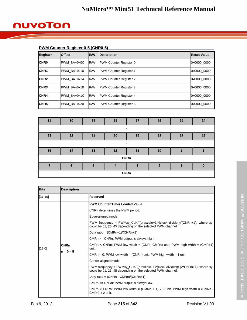
NuMicro™ Mini51 Technical Reference Manual
Feb 9, 2012 Page 215 of 342 Revision V1.03
NU
MIC
RO
™ M
INI5
1 T
EC
HN
ICA
L R
EF
ER
EN
CE
MA
NU
AL
PWM Counter Register 0-5 (CNR0-5)
Register Offset R/W Description Reset Value
CNR0 PWM_BA+0x0C R/W PWM Counter Register 0 0x0000_0000
CNR1 PWM_BA+0x10 R/W PWM Counter Register 1 0x0000_0000
CNR2 PWM_BA+0x14 R/W PWM Counter Register 2 0x0000_0000
CNR3 PWM_BA+0x18 R/W PWM Counter Register 3 0x0000_0000
CNR4 PWM_BA+0x1C R/W PWM Counter Register 4 0x0000_0000
CNR5 PWM_BA+0x20 R/W PWM Counter Register 5 0x0000_0000
31 30 29 28 27 26 25 24
-
23 22 21 20 19 18 17 16
-
15 14 13 12 11 10 9 8
CNRn
7 6 5 4 3 2 1 0
CNRn
Bits Description
[31:16] - Reserved
[15:0] CNRn
n = 0 – 5
PWM Counter/Timer Loaded Value
CNRn determines the PWM period.
Edge-aligned mode:
PWM frequency = PWMxy_CLK/((prescale+1)*(clock divider))/(CNRn+1); where xy, could be 01, 23, 45 depending on the selected PWM channel.
Duty ratio = (CMRn+1)/(CNRn+1).
CMRn >= CNRn: PWM output is always high.
CMRn < CNRn: PWM low width = (CNRn-CMRn) unit; PWM high width = (CMR+1) unit.
CMRn = 0: PWM low width = (CNRn) unit; PWM high width = 1 unit.
Center-aligned mode:
PWM frequency = PWMxy_CLK/((prescale+1)*(clock divider))/ (2*CNRn+1); where xy, could be 01, 23, 45 depending on the selected PWM channel.
Duty ratio = (CNRn - CMRn)/(CNRn+1).
CMRn >= CNRn: PWM output is always low.
CMRn < CNRn: PWM low width = (CMRn + 1) x 2 unit; PWM high width = (CNRn - CMRn) x 2 unit.
NuMicro™ Mini51 Technical Reference Manual
Feb 9, 2012 Page 216 of 342 Revision V1.03
NU
MIC
RO
™ M
INI5
1 T
EC
HN
ICA
L R
EF
ER
EN
CE
MA
NU
AL
Bits Description
CMRn = 0: PWM low width = 2 unit; PWM high width = (CNRn) x 2 unit.
(Unit = one PWM clock cycle)
Note: Any write to CNRn will take effect in next PWM cycle.
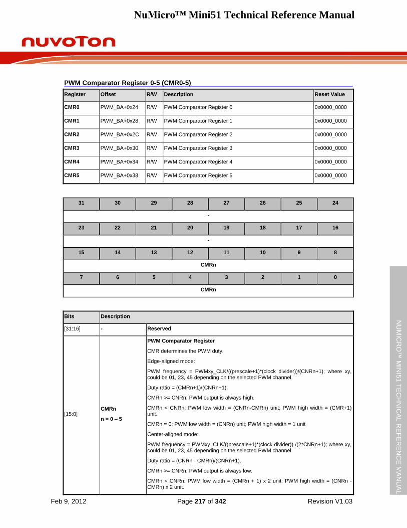
NuMicro™ Mini51 Technical Reference Manual
Feb 9, 2012 Page 217 of 342 Revision V1.03
NU
MIC
RO
™ M
INI5
1 T
EC
HN
ICA
L R
EF
ER
EN
CE
MA
NU
AL
PWM Comparator Register 0-5 (CMR0-5)
Register Offset R/W Description Reset Value
CMR0 PWM_BA+0x24 R/W PWM Comparator Register 0 0x0000_0000
CMR1 PWM_BA+0x28 R/W PWM Comparator Register 1 0x0000_0000
CMR2 PWM_BA+0x2C R/W PWM Comparator Register 2 0x0000_0000
CMR3 PWM_BA+0x30 R/W PWM Comparator Register 3 0x0000_0000
CMR4 PWM_BA+0x34 R/W PWM Comparator Register 4 0x0000_0000
CMR5 PWM_BA+0x38 R/W PWM Comparator Register 5 0x0000_0000
31 30 29 28 27 26 25 24
-
23 22 21 20 19 18 17 16
-
15 14 13 12 11 10 9 8
CMRn
7 6 5 4 3 2 1 0
CMRn
Bits Description
[31:16] - Reserved
[15:0] CMRn
n = 0 – 5
PWM Comparator Register
CMR determines the PWM duty.
Edge-aligned mode:
PWM frequency = PWMxy_CLK/((prescale+1)*(clock divider))/(CNRn+1); where xy, could be 01, 23, 45 depending on the selected PWM channel.
Duty ratio = (CMRn+1)/(CNRn+1).
CMRn >= CNRn: PWM output is always high.
CMRn < CNRn: PWM low width = (CNRn-CMRn) unit; PWM high width = (CMR+1) unit.
CMRn = 0: PWM low width = (CNRn) unit; PWM high width = 1 unit
Center-aligned mode:
PWM frequency = PWMxy_CLK/((prescale+1)*(clock divider)) /(2*CNRn+1); where xy, could be 01, 23, 45 depending on the selected PWM channel.
Duty ratio = (CNRn - CMRn)/(CNRn+1).
CMRn >= CNRn: PWM output is always low.
CMRn < CNRn: PWM low width = (CMRn + 1) x 2 unit; PWM high width = (CNRn - CMRn) x 2 unit.
NuMicro™ Mini51 Technical Reference Manual
Feb 9, 2012 Page 218 of 342 Revision V1.03
NU
MIC
RO
™ M
INI5
1 T
EC
HN
ICA
L R
EF
ER
EN
CE
MA
NU
AL
Bits Description
CMRn = 0: PWM low width = 2 unit; PWM high width = (CNRn) x 2 unit
(Unit = One PWM clock cycle)
Note: Any write to CNRn will take effect in the next PWM cycle.
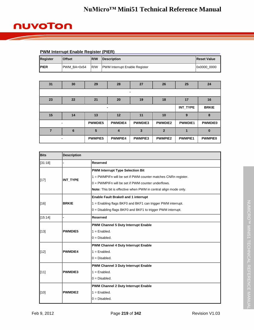
NuMicro™ Mini51 Technical Reference Manual
Feb 9, 2012 Page 219 of 342 Revision V1.03
NU
MIC
RO
™ M
INI5
1 T
EC
HN
ICA
L R
EF
ER
EN
CE
MA
NU
AL
PWM Interrupt Enable Register (PIER)
Register Offset R/W Description Reset Value
PIER PWM_BA+0x54 R/W PWM Interrupt Enable Register 0x0000_0000
31 30 29 28 27 26 25 24
-
23 22 21 20 19 18 17 16
- INT_TYPE BRKIE
15 14 13 12 11 10 9 8
- PWMDIE5 PWMDIE4 PWMDIE3 PWMDIE2 PWMDIE1 PWMDIE0
7 6 5 4 3 2 1 0
- PWMPIE5 PWMPIE4 PWMPIE3 PWMPIE2 PWMPIE1 PWMPIE0
Bits Description
[31:18] - Reserved
[17] INT_TYPE
PWM Interrupt Type Selection Bit
1 = PWMPIFn will be set if PWM counter matches CNRn register.
0 = PWMPIFn will be set if PWM counter underflows.
Note: This bit is effective when PWM in central align mode only.
[16] BRKIE
Enable Fault Brake0 and 1 interrupt
1 = Enabling flags BKF0 and BKF1 can trigger PWM interrupt.
0 = Disabling flags BKF0 and BKF1 to trigger PWM interrupt.
[15:14] - Reserved
[13] PWMDIE5
PWM Channel 5 Duty Interrupt Enable
1 = Enabled.
0 = Disabled.
[12] PWMDIE4
PWM Channel 4 Duty Interrupt Enable
1 = Enabled.
0 = Disabled.
[11] PWMDIE3
PWM Channel 3 Duty Interrupt Enable
1 = Enabled.
0 = Disabled.
[10] PWMDIE2
PWM Channel 2 Duty Interrupt Enable
1 = Enabled.
0 = Disabled.
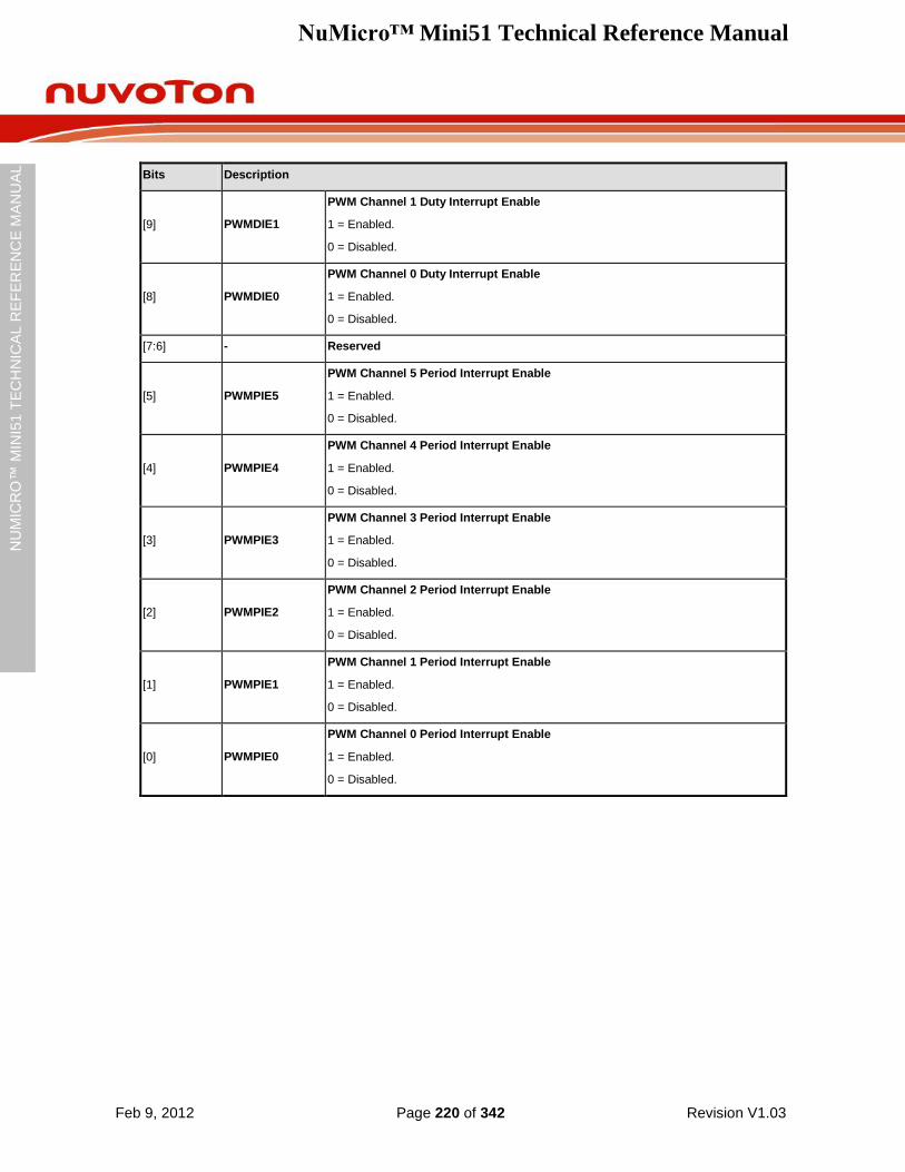
NuMicro™ Mini51 Technical Reference Manual
Feb 9, 2012 Page 220 of 342 Revision V1.03
NU
MIC
RO
™ M
INI5
1 T
EC
HN
ICA
L R
EF
ER
EN
CE
MA
NU
AL
Bits Description
[9] PWMDIE1
PWM Channel 1 Duty Interrupt Enable
1 = Enabled.
0 = Disabled.
[8] PWMDIE0
PWM Channel 0 Duty Interrupt Enable
1 = Enabled.
0 = Disabled.
[7:6] - Reserved
[5] PWMPIE5
PWM Channel 5 Period Interrupt Enable
1 = Enabled.
0 = Disabled.
[4] PWMPIE4
PWM Channel 4 Period Interrupt Enable
1 = Enabled.
0 = Disabled.
[3] PWMPIE3
PWM Channel 3 Period Interrupt Enable
1 = Enabled.
0 = Disabled.
[2] PWMPIE2
PWM Channel 2 Period Interrupt Enable
1 = Enabled.
0 = Disabled.
[1] PWMPIE1
PWM Channel 1 Period Interrupt Enable
1 = Enabled.
0 = Disabled.
[0] PWMPIE0
PWM Channel 0 Period Interrupt Enable
1 = Enabled.
0 = Disabled.
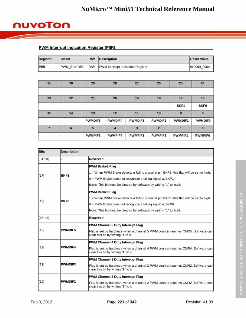
NuMicro™ Mini51 Technical Reference Manual
Feb 9, 2012 Page 221 of 342 Revision V1.03
NU
MIC
RO
™ M
INI5
1 T
EC
HN
ICA
L R
EF
ER
EN
CE
MA
NU
AL
PWM Interrupt Indication Register (PIIR)
Register Offset R/W Description Reset Value
PIIR PWM_BA+0x58 R/W PWM Interrupt Indication Register 0x0000_0000
31 30 29 28 27 26 25 24
-
23 22 21 20 19 18 17 16
- BKF1 BKF0
15 14 13 12 11 10 9 8
- PWMDIF5 PWMDIF4 PWMDIF3 PWMDIF2 PWMDIF1 PWMDIF0
7 6 5 4 3 2 1 0
- PWMPIF5 PWMPIF4 PWMPIF3 PWMPIF2 PWMPIF1 PWMPIF0
Bits Description
[31:18] - Reserved
[17] BKF1
PWM Brake1 Flag
1 = When PWM Brake detects a falling signal at pin BKP1, this flag will be set to high.
0 = PWM Brake does not recognize a falling signal at BKP1.
Note: This bit must be cleared by software by writing “1” to itself.
[16] BKF0
PWM Brake0 Flag
1 = When PWM Brake detects a falling signal at pin BKP0, this flag will be set to high.
0 = PWM Brake does not recognize a falling signal at BKP0.
Note: This bit must be cleared by software by writing “1” to itself.
[15:14] - Reserved
[13] PWMDIF5
PWM Channel 5 Duty Interrupt Flag
Flag is set by hardware when a channel 5 PWM counter reaches CMR5. Software can clear this bit by writing “1”to it.
[12] PWMDIF4
PWM Channel 4 Duty Interrupt Flag
Flag is set by hardware when a channel 4 PWM counter reaches CMR4. Software can clear this bit by writing “1” to it.
[11] PWMDIF3
PWM Channel 3 Duty Interrupt Flag
Flag is set by hardware when a channel 3 PWM counter reaches CMR3. Software can clear this bit by writing “1” to it.
[10] PWMDIF2
PWM Channel 2 Duty Interrupt Flag
Flag is set by hardware when a channel 2 PWM counter reaches CMR2. Software can clear this bit by writing “1” to it.
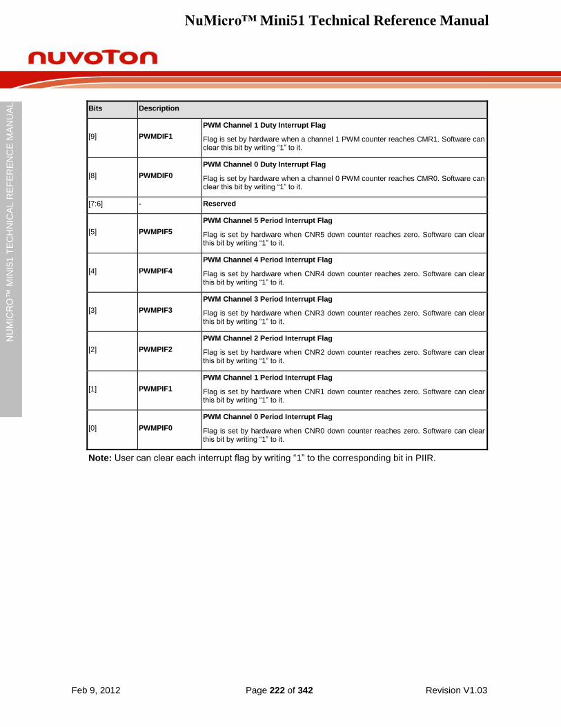
NuMicro™ Mini51 Technical Reference Manual
Feb 9, 2012 Page 222 of 342 Revision V1.03
NU
MIC
RO
™ M
INI5
1 T
EC
HN
ICA
L R
EF
ER
EN
CE
MA
NU
AL
Bits Description
[9] PWMDIF1
PWM Channel 1 Duty Interrupt Flag
Flag is set by hardware when a channel 1 PWM counter reaches CMR1. Software can clear this bit by writing “1” to it.
[8] PWMDIF0
PWM Channel 0 Duty Interrupt Flag
Flag is set by hardware when a channel 0 PWM counter reaches CMR0. Software can clear this bit by writing “1” to it.
[7:6] - Reserved
[5] PWMPIF5
PWM Channel 5 Period Interrupt Flag
Flag is set by hardware when CNR5 down counter reaches zero. Software can clear this bit by writing “1” to it.
[4] PWMPIF4
PWM Channel 4 Period Interrupt Flag
Flag is set by hardware when CNR4 down counter reaches zero. Software can clear this bit by writing “1” to it.
[3] PWMPIF3
PWM Channel 3 Period Interrupt Flag
Flag is set by hardware when CNR3 down counter reaches zero. Software can clear this bit by writing “1” to it.
[2] PWMPIF2
PWM Channel 2 Period Interrupt Flag
Flag is set by hardware when CNR2 down counter reaches zero. Software can clear this bit by writing “1” to it.
[1] PWMPIF1
PWM Channel 1 Period Interrupt Flag
Flag is set by hardware when CNR1 down counter reaches zero. Software can clear this bit by writing “1” to it.
[0] PWMPIF0
PWM Channel 0 Period Interrupt Flag
Flag is set by hardware when CNR0 down counter reaches zero. Software can clear this bit by writing “1” to it.
Note: User can clear each interrupt flag by writing “1” to the corresponding bit in PIIR.
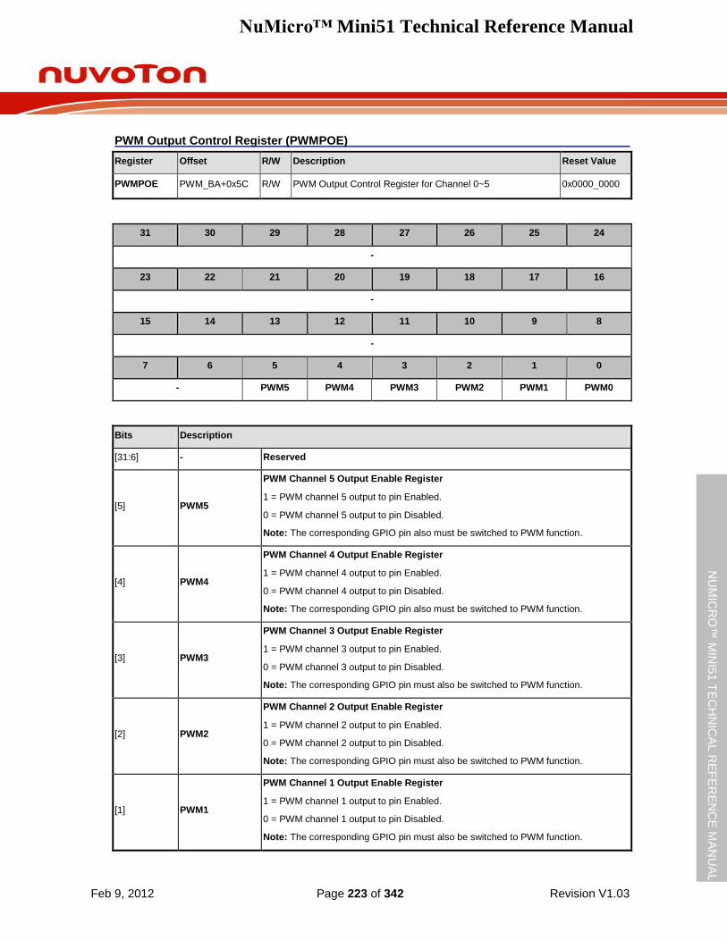
NuMicro™ Mini51 Technical Reference Manual
Feb 9, 2012 Page 223 of 342 Revision V1.03
NU
MIC
RO
™ M
INI5
1 T
EC
HN
ICA
L R
EF
ER
EN
CE
MA
NU
AL
PWM Output Control Register (PWMPOE)
Register Offset R/W Description Reset Value
PWMPOE PWM_BA+0x5C R/W PWM Output Control Register for Channel 0~5 0x0000_0000
31 30 29 28 27 26 25 24
-
23 22 21 20 19 18 17 16
-
15 14 13 12 11 10 9 8
-
7 6 5 4 3 2 1 0
- PWM5 PWM4 PWM3 PWM2 PWM1 PWM0
Bits Description
[31:6] - Reserved
[5] PWM5
PWM Channel 5 Output Enable Register
1 = PWM channel 5 output to pin Enabled.
0 = PWM channel 5 output to pin Disabled.
Note: The corresponding GPIO pin also must be switched to PWM function.
[4] PWM4
PWM Channel 4 Output Enable Register
1 = PWM channel 4 output to pin Enabled.
0 = PWM channel 4 output to pin Disabled.
Note: The corresponding GPIO pin also must be switched to PWM function.
[3] PWM3
PWM Channel 3 Output Enable Register
1 = PWM channel 3 output to pin Enabled.
0 = PWM channel 3 output to pin Disabled.
Note: The corresponding GPIO pin must also be switched to PWM function.
[2] PWM2
PWM Channel 2 Output Enable Register
1 = PWM channel 2 output to pin Enabled.
0 = PWM channel 2 output to pin Disabled.
Note: The corresponding GPIO pin must also be switched to PWM function.
[1] PWM1
PWM Channel 1 Output Enable Register
1 = PWM channel 1 output to pin Enabled.
0 = PWM channel 1 output to pin Disabled.
Note: The corresponding GPIO pin must also be switched to PWM function.
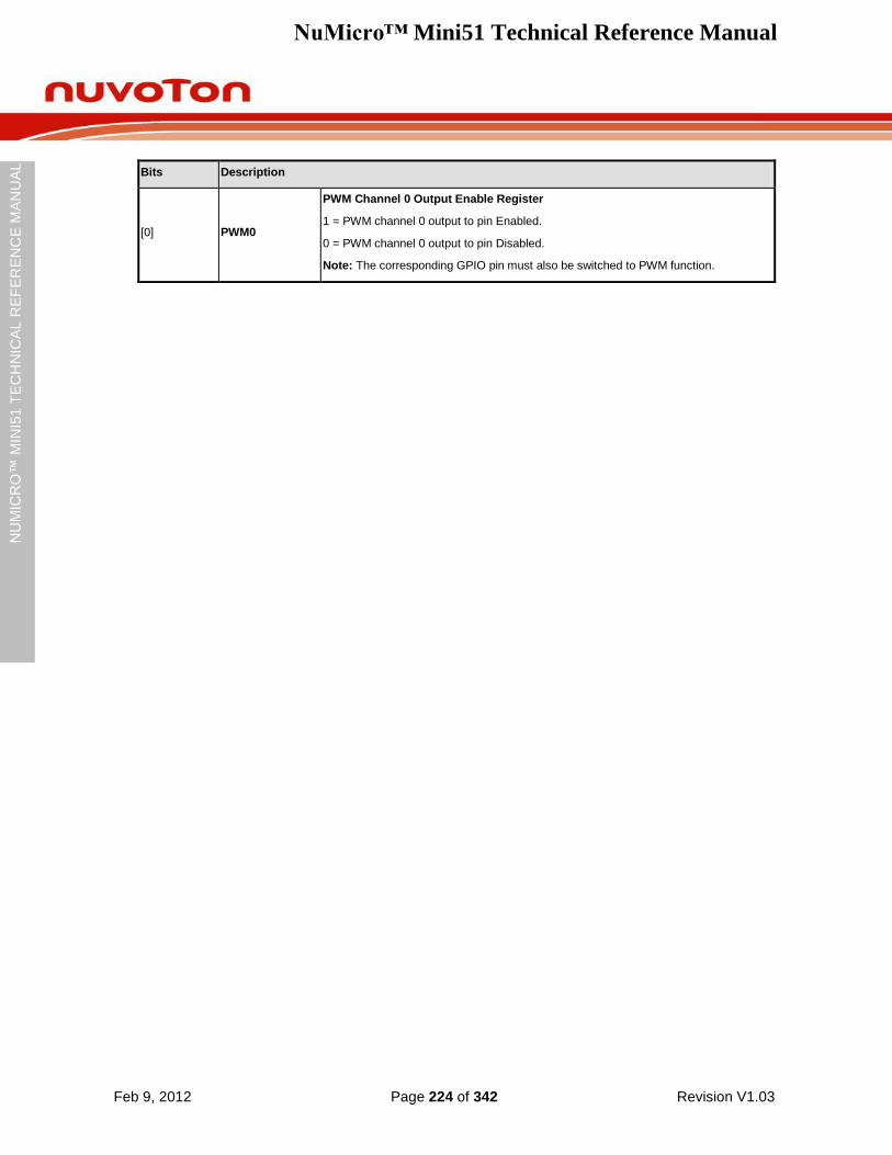
NuMicro™ Mini51 Technical Reference Manual
Feb 9, 2012 Page 224 of 342 Revision V1.03
NU
MIC
RO
™ M
INI5
1 T
EC
HN
ICA
L R
EF
ER
EN
CE
MA
NU
AL
Bits Description
[0] PWM0
PWM Channel 0 Output Enable Register
1 = PWM channel 0 output to pin Enabled.
0 = PWM channel 0 output to pin Disabled.
Note: The corresponding GPIO pin must also be switched to PWM function.
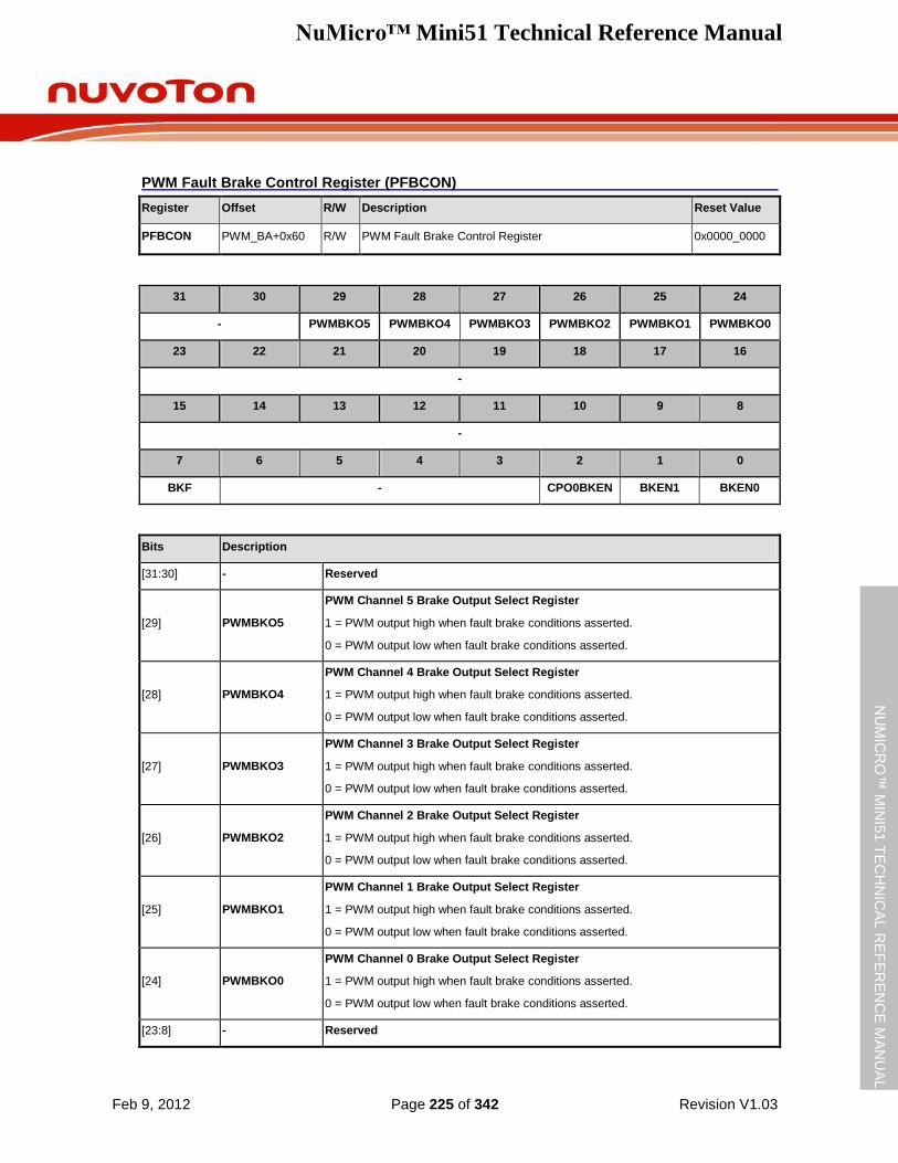
NuMicro™ Mini51 Technical Reference Manual
Feb 9, 2012 Page 225 of 342 Revision V1.03
NU
MIC
RO
™ M
INI5
1 T
EC
HN
ICA
L R
EF
ER
EN
CE
MA
NU
AL
PWM Fault Brake Control Register (PFBCON)
Register Offset R/W Description Reset Value
PFBCON PWM_BA+0x60 R/W PWM Fault Brake Control Register 0x0000_0000
31 30 29 28 27 26 25 24
- PWMBKO5 PWMBKO4 PWMBKO3 PWMBKO2 PWMBKO1 PWMBKO0
23 22 21 20 19 18 17 16
-
15 14 13 12 11 10 9 8
-
7 6 5 4 3 2 1 0
BKF - CPO0BKEN BKEN1 BKEN0
Bits Description
[31:30] - Reserved
[29] PWMBKO5
PWM Channel 5 Brake Output Select Register
1 = PWM output high when fault brake conditions asserted.
0 = PWM output low when fault brake conditions asserted.
[28] PWMBKO4
PWM Channel 4 Brake Output Select Register
1 = PWM output high when fault brake conditions asserted.
0 = PWM output low when fault brake conditions asserted.
[27] PWMBKO3
PWM Channel 3 Brake Output Select Register
1 = PWM output high when fault brake conditions asserted.
0 = PWM output low when fault brake conditions asserted.
[26] PWMBKO2
PWM Channel 2 Brake Output Select Register
1 = PWM output high when fault brake conditions asserted.
0 = PWM output low when fault brake conditions asserted.
[25] PWMBKO1
PWM Channel 1 Brake Output Select Register
1 = PWM output high when fault brake conditions asserted.
0 = PWM output low when fault brake conditions asserted.
[24] PWMBKO0
PWM Channel 0 Brake Output Select Register
1 = PWM output high when fault brake conditions asserted.
0 = PWM output low when fault brake conditions asserted.
[23:8] - Reserved
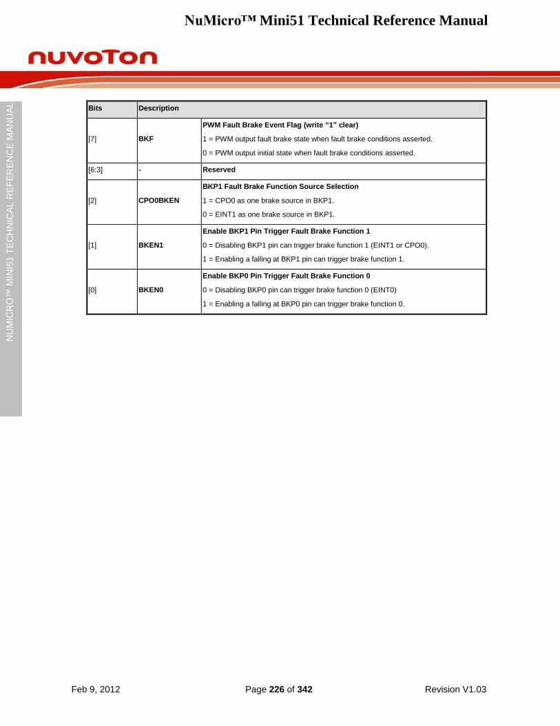
NuMicro™ Mini51 Technical Reference Manual
Feb 9, 2012 Page 226 of 342 Revision V1.03
NU
MIC
RO
™ M
INI5
1 T
EC
HN
ICA
L R
EF
ER
EN
CE
MA
NU
AL
Bits Description
[7] BKF
PWM Fault Brake Event Flag (write “1” clear)
1 = PWM output fault brake state when fault brake conditions asserted.
0 = PWM output initial state when fault brake conditions asserted.
[6:3] - Reserved
[2] CPO0BKEN
BKP1 Fault Brake Function Source Selection
1 = CPO0 as one brake source in BKP1.
0 = EINT1 as one brake source in BKP1.
[1] BKEN1
Enable BKP1 Pin Trigger Fault Brake Function 1
0 = Disabling BKP1 pin can trigger brake function 1 (EINT1 or CPO0).
1 = Enabling a falling at BKP1 pin can trigger brake function 1.
[0] BKEN0
Enable BKP0 Pin Trigger Fault Brake Function 0
0 = Disabling BKP0 pin can trigger brake function 0 (EINT0)
1 = Enabling a falling at BKP0 pin can trigger brake function 0.

NuMicro™ Mini51 Technical Reference Manual
Feb 9, 2012 Page 227 of 342 Revision V1.03
NU
MIC
RO
™ M
INI5
1 T
EC
HN
ICA
L R
EF
ER
EN
CE
MA
NU
AL
PWM Dead-Zone Interval Register (PDZIR)
Register Offset R/W Description Reset Value
PDZIR PWM_BA+0x64 R/W PWM Dead-zone Interval Register 0x0000_0000
31 30 29 28 27 26 25 24
-
23 22 21 20 19 18 17 16
DZI45
15 14 13 12 11 10 9 8
DZI23
7 6 5 4 3 2 1 0
DZI01
Bits Description
[31:24] - Reserved
[23:16] DZI45[7:0]
Dead-zone Interval Register for Pair of channel4 and channel5 (PWM4 and PWM5 pair).
These 8 bits determine the dead-zone length.
The unit time of dead-zone length is received from corresponding CSR bits.
[15:8] DZI23[7:0]
Dead-zone Interval Register for Pair of channel2 and channel3 (PWM2 and PWM3 pair).
These 8 bits determine the dead-zone length.
The unit time of dead-zone length is received from corresponding CSR bits.
[7:0] DZI01[7:0]
Dead-zone Interval Register for Pair of channel0 and channel1 (PWM0 and PWM1 pair).
These 8 bits determine the dead-zone length.
The unit time of dead-zone length is received from corresponding CSR bits.
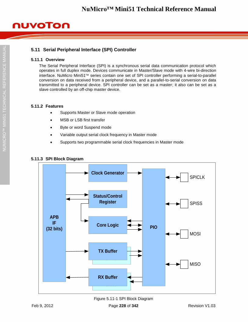
NuMicro™ Mini51 Technical Reference Manual
Feb 9, 2012 Page 228 of 342 Revision V1.03
NU
MIC
RO
™ M
INI5
1 T
EC
HN
ICA
L R
EF
ER
EN
CE
MA
NU
AL
5.11 Serial Peripheral Interface (SPI) Controller
5.11.1 Overview
The Serial Peripheral Interface (SPI) is a synchronous serial data communication protocol which operates in full duplex mode. Devices communicate in Master/Slave mode with 4-wire bi-direction
interface. NuMicro Mini51 series contain one set of SPI controller performing a serial-to-parallel conversion on data received from a peripheral device, and a parallel-to-serial conversion on data transmitted to a peripheral device. SPI controller can be set as a master; it also can be set as a slave controlled by an off-chip master device.
5.11.2 Features
Supports Master or Slave mode operation
MSB or LSB first transfer
Byte or word Suspend mode
Variable output serial clock frequency in Master mode
Supports two programmable serial clock frequencies in Master mode
5.11.3 SPI Block Diagram
APB
IF
(32 bits)
Clock Generator
Status/Control
Register
Core Logic
TX Bufer/
Shifter
RX Bufer/
Shifter
TX Buffer
RX Buffer
PIO
MISO
MOSI
SPICLK
SPISS
Figure 5.11-1 SPI Block Diagram
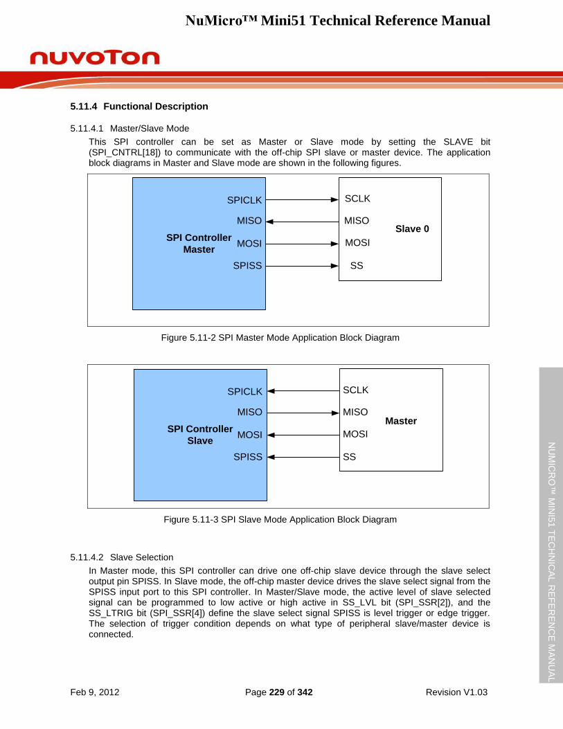
NuMicro™ Mini51 Technical Reference Manual
Feb 9, 2012 Page 229 of 342 Revision V1.03
NU
MIC
RO
™ M
INI5
1 T
EC
HN
ICA
L R
EF
ER
EN
CE
MA
NU
AL
5.11.4 Functional Description
5.11.4.1 Master/Slave Mode
This SPI controller can be set as Master or Slave mode by setting the SLAVE bit (SPI_CNTRL[18]) to communicate with the off-chip SPI slave or master device. The application block diagrams in Master and Slave mode are shown in the following figures.
SPI Controller
Master
SPICLK
MISO
MOSI
SPISS
SCLK
MISO
MOSI
SS
Slave 0
Figure 5.11-2 SPI Master Mode Application Block Diagram
SPI Controller
Slave
SPICLK
MISO
MOSI
SPISS
SCLK
MISO
MOSI
SS
Master
Figure 5.11-3 SPI Slave Mode Application Block Diagram
5.11.4.2 Slave Selection
In Master mode, this SPI controller can drive one off-chip slave device through the slave select output pin SPISS. In Slave mode, the off-chip master device drives the slave select signal from the SPISS input port to this SPI controller. In Master/Slave mode, the active level of slave selected signal can be programmed to low active or high active in SS_LVL bit (SPI_SSR[2]), and the SS_LTRIG bit (SPI_SSR[4]) define the slave select signal SPISS is level trigger or edge trigger. The selection of trigger condition depends on what type of peripheral slave/master device is connected.
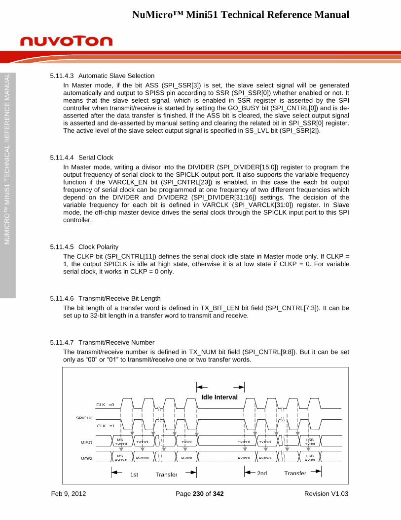
NuMicro™ Mini51 Technical Reference Manual
Feb 9, 2012 Page 230 of 342 Revision V1.03
NU
MIC
RO
™ M
INI5
1 T
EC
HN
ICA
L R
EF
ER
EN
CE
MA
NU
AL
5.11.4.3 Automatic Slave Selection
In Master mode, if the bit ASS (SPI_SSR[3]) is set, the slave select signal will be generated automatically and output to SPISS pin according to SSR (SPI_SSR[0]) whether enabled or not. It means that the slave select signal, which is enabled in SSR register is asserted by the SPI controller when transmit/receive is started by setting the GO_BUSY bit (SPI_CNTRL[0]) and is de-asserted after the data transfer is finished. If the ASS bit is cleared, the slave select output signal is asserted and de-asserted by manual setting and clearing the related bit in SPI_SSR[0] register. The active level of the slave select output signal is specified in SS_LVL bit (SPI_SSR[2]).
5.11.4.4 Serial Clock
In Master mode, writing a divisor into the DIVIDER (SPI_DIVIDER[15:0]) register to program the output frequency of serial clock to the SPICLK output port. It also supports the variable frequency function if the VARCLK_EN bit (SPI_CNTRL[23]) is enabled, in this case the each bit output frequency of serial clock can be programmed at one frequency of two different frequencies which depend on the DIVIDER and DIVIDER2 (SPI_DIVIDER[31:16]) settings. The decision of the variable frequency for each bit is defined in VARCLK (SPI_VARCLK[31:0]) register. In Slave mode, the off-chip master device drives the serial clock through the SPICLK input port to this SPI controller.
5.11.4.5 Clock Polarity
The CLKP bit (SPI_CNTRL[11]) defines the serial clock idle state in Master mode only. If CLKP = 1, the output SPICLK is idle at high state, otherwise it is at low state if CLKP = 0. For variable serial clock, it works in CLKP = 0 only.
5.11.4.6 Transmit/Receive Bit Length
The bit length of a transfer word is defined in TX_BIT_LEN bit field (SPI_CNTRL[7:3]). It can be set up to 32-bit length in a transfer word to transmit and receive.
5.11.4.7 Transmit/Receive Number
The transmit/receive number is defined in TX_NUM bit field (SPI_CNTRL[9:8]). But it can be set only as “00” or “01” to transmit/receive one or two transfer words.
SPICLK
MOSI
MISO Tx 0 [ 30 ] Tx 0 [ 0 ] Tx 1 [ 31 ] Tx 1 [ 30 ] LSB Tx 1 [ 0 ] MS
B Tx 0 [ 31 ]
Rx 0 [ 30 ] Rx 0 [ 0 ] Rx 1 [ 31 ] Rx 1 [ 30 ] LSB Rx 1 [ 0 ] MS
B Rx 0 [ 31 ]
CLKP = 0
CLKP = 1
Idle Interval
1 st Transfer Word
2 nd Transfer Word
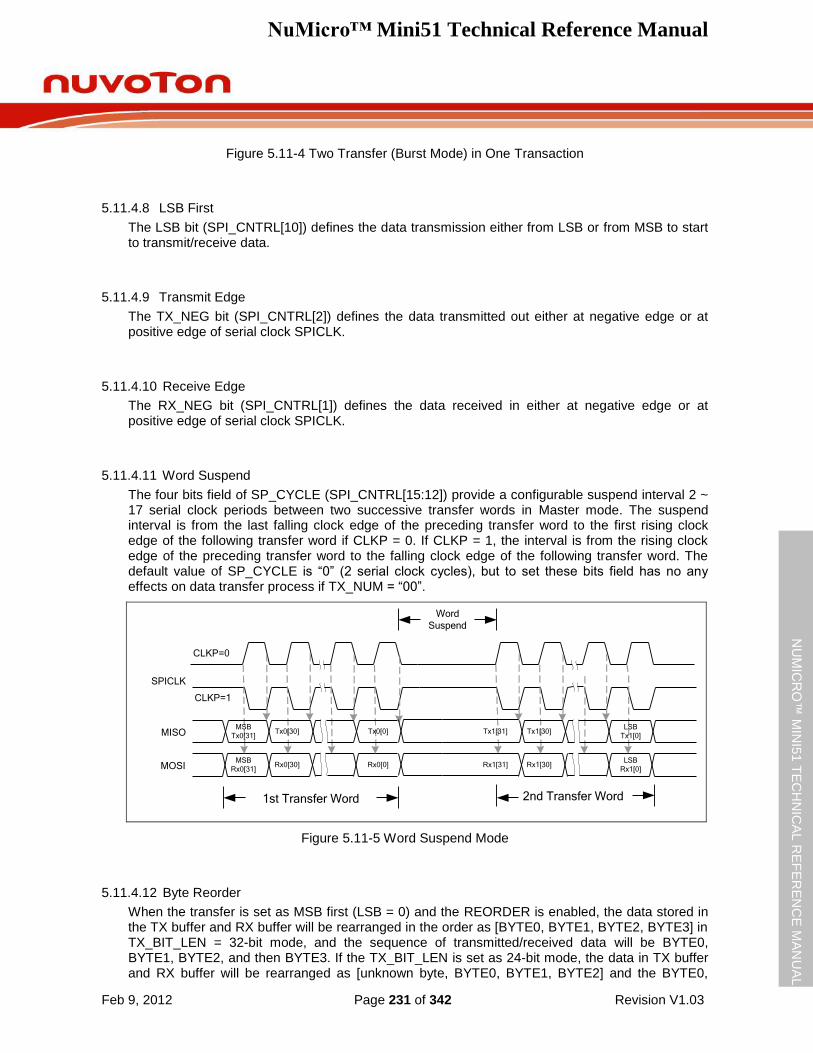
NuMicro™ Mini51 Technical Reference Manual
Feb 9, 2012 Page 231 of 342 Revision V1.03
NU
MIC
RO
™ M
INI5
1 T
EC
HN
ICA
L R
EF
ER
EN
CE
MA
NU
AL
Figure 5.11-4 Two Transfer (Burst Mode) in One Transaction
5.11.4.8 LSB First
The LSB bit (SPI_CNTRL[10]) defines the data transmission either from LSB or from MSB to start to transmit/receive data.
5.11.4.9 Transmit Edge
The TX_NEG bit (SPI_CNTRL[2]) defines the data transmitted out either at negative edge or at positive edge of serial clock SPICLK.
5.11.4.10 Receive Edge
The RX_NEG bit (SPI_CNTRL[1]) defines the data received in either at negative edge or at positive edge of serial clock SPICLK.
5.11.4.11 Word Suspend
The four bits field of SP_CYCLE (SPI_CNTRL[15:12]) provide a configurable suspend interval 2 ~ 17 serial clock periods between two successive transfer words in Master mode. The suspend interval is from the last falling clock edge of the preceding transfer word to the first rising clock edge of the following transfer word if CLKP = 0. If CLKP = 1, the interval is from the rising clock edge of the preceding transfer word to the falling clock edge of the following transfer word. The default value of SP_CYCLE is “0” (2 serial clock cycles), but to set these bits field has no any effects on data transfer process if TX_NUM = “00”.
SPICLK
MOSI
MISO Tx0[30] Tx0[0] Tx1[31] Tx1[30]LSB
Tx1[0]
MSB
Tx0[31]
Rx0[30] Rx0[0] Rx1[31] Rx1[30]LSB
Rx1[0]
MSB
Rx0[31]
CLKP=0
CLKP=1
Word
Suspend
1st Transfer Word 2nd Transfer Word
Figure 5.11-5 Word Suspend Mode
5.11.4.12 Byte Reorder
When the transfer is set as MSB first (LSB = 0) and the REORDER is enabled, the data stored in the TX buffer and RX buffer will be rearranged in the order as [BYTE0, BYTE1, BYTE2, BYTE3] in TX_BIT_LEN = 32-bit mode, and the sequence of transmitted/received data will be BYTE0, BYTE1, BYTE2, and then BYTE3. If the TX_BIT_LEN is set as 24-bit mode, the data in TX buffer and RX buffer will be rearranged as [unknown byte, BYTE0, BYTE1, BYTE2] and the BYTE0,
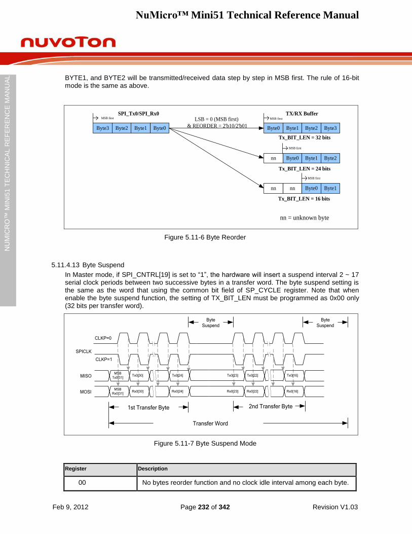
NuMicro™ Mini51 Technical Reference Manual
Feb 9, 2012 Page 232 of 342 Revision V1.03
NU
MIC
RO
™ M
INI5
1 T
EC
HN
ICA
L R
EF
ER
EN
CE
MA
NU
AL
BYTE1, and BYTE2 will be transmitted/received data step by step in MSB first. The rule of 16-bit mode is the same as above.
Byte3 Byte0Byte1Byte2
SPI_Tx0/SPI_Rx0 TX/RX Buffer
Byte3Byte0 Byte1 Byte2
LSB = 0 (MSB first)
& REORDER = 2'b10/2'b01
nn Byte0 Byte1 Byte2
nn Byte0 Byte1nn
Tx_BIT_LEN = 24 bits
Tx_BIT_LEN = 16 bits
Tx_BIT_LEN = 32 bits
MSB first
MSB first
MSB first
MSB first
nn = unknown byte
Figure 5.11-6 Byte Reorder
5.11.4.13 Byte Suspend
In Master mode, if SPI_CNTRL[19] is set to “1”, the hardware will insert a suspend interval 2 ~ 17 serial clock periods between two successive bytes in a transfer word. The byte suspend setting is the same as the word that using the common bit field of SP_CYCLE register. Note that when enable the byte suspend function, the setting of TX_BIT_LEN must be programmed as 0x00 only (32 bits per transfer word).
SPICLK
MOSI
MISO Tx0[30] Tx0[24] Tx0[23] Tx0[22] Tx0[16]MSB
Tx0[31]
Rx0[30] Rx0[24] Rx0[23] Rx0[22] Rx0[16]MSB
Rx0[31]
CLKP=0
CLKP=1
Byte
Suspend
1st Transfer Byte 2nd Transfer Byte
Byte
Suspend
Transfer Word
Figure 5.11-7 Byte Suspend Mode
Register Description
00 No bytes reorder function and no clock idle interval among each byte.
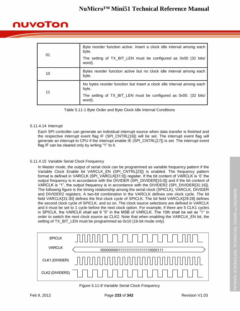
NuMicro™ Mini51 Technical Reference Manual
Feb 9, 2012 Page 233 of 342 Revision V1.03
NU
MIC
RO
™ M
INI5
1 T
EC
HN
ICA
L R
EF
ER
EN
CE
MA
NU
AL
01
Byte reorder function active. Insert a clock idle interval among each byte.
The setting of TX_BIT_LEN must be configured as 0x00 (32 bits/ word).
10 Bytes reorder function active but no clock idle interval among each byte.
11
No bytes reorder function but insert a clock idle interval among each byte.
The setting of TX_BIT_LEN must be configured as 0x00. (32 bits/ word).
Table 5.11-1 Byte Order and Byte Clock Idle Internal Conditions
5.11.4.14 Interrupt
Each SPI controller can generate an individual interrupt source when data transfer is finished and the respective interrupt event flag IF (SPI_CNTRL[16]) will be set. The interrupt event flag will generate an interrupt to CPU if the interrupt enable IE (SPI_CNTRL[17]) is set. The interrupt event flag IF can be cleared only by writing “1” to it.
5.11.4.15 Variable Serial Clock Frequency
In Master mode, the output of serial clock can be programmed as variable frequency pattern if the Variable Clock Enable bit VARCLK_EN (SPI_CNTRL[23]) is enabled. The frequency pattern format is defined in VARCLK (SPI_VARCLK[31:0]) register. If the bit content of VARCLK is „0‟ the output frequency is in accordance with the DIVIDER (SPI_DIVIDER[15:0]) and if the bit content of VARCLK is “1”, the output frequency is in accordance with the DIVIDER2 (SPI_DIVIDER[31:16]). The following figure is the timing relationship among the serial clock (SPICLK), VARCLK, DIVIDER and DIVIDER2 registers. A two-bit combination in the VARCLK defines one clock cycle. The bit field VARCLK[31:30] defines the first clock cycle of SPICLK. The bit field VARCLK[29:28] defines the second clock cycle of SPICLK, and so on. The clock source selections are defined in VARCLK and it must be set to 1 cycle before the next clock option. For example, if there are 5 CLK1 cycles in SPICLK, the VARCLK shall set 9 ”0” in the MSB of VARCLK. The 10th shall be set as ”1" in order to switch the next clock source as CLK2. Note that when enabling the VARCLK_EN bit, the setting of TX_BIT_LEN must be programmed as 0x10 (16-bit mode only).
00000000011111111111111110000111
SPICLK
VARCLK
CLK1 (DIVIDER)
CLK2 (DIVIDER2)
Figure 5.11-8 Variable Serial Clock Frequency
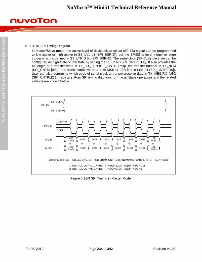
NuMicro™ Mini51 Technical Reference Manual
Feb 9, 2012 Page 234 of 342 Revision V1.03
NU
MIC
RO
™ M
INI5
1 T
EC
HN
ICA
L R
EF
ER
EN
CE
MA
NU
AL
5.11.4.16 SPI Timing Diagram
In Master/Slave mode, the active level of device/slave select (SPISS) signal can be programmed to low active or high active in SS_LVL bit (SPI_SSR[2]), but the SPISS is level trigger or edge trigger which is defined in SS_LTRIG bit (SPI_SSR[4]). The serial clock (SPICLK) idle state can be configured as high state or low state by setting the CLKP bit (SPI_CNTRL[11]). It also provides the bit length of a transfer word in TX_BIT_LEN (SPI_CNTRL[7:3]), the transfer number in TX_NUM (SPI_CNTRL[9:8]), and transmit/receive data from MSB or LSB first in LSB bit (SPI_CNTRL[10]). User can also determine which edge of serial clock to transmit/receive data in TX_NEG/RX_NEG (SPI_CNTRL[2:1]) registers. Four SPI timing diagrams for master/slave operations and the related settings are shown below.
SPICLK
MISO
Master Mode: CNTRL[SLAVE]=0, CNTRL[LSB]=0, CNTRL[Tx_NUM]=0x0, CNTRL[Tx_BIT_LEN]=0x08
MOSI Tx0[6] Tx0[5] Tx0[4] Tx0[3] Tx0[2] Tx0[1]LSB
Tx0[0]
MSB
Tx0[7]
Rx0[6] Rx0[5] Rx0[4] Rx0[3] Rx0[2] Rx0[1]LSB
Rx0[0]
MSB
Rx0[7]
CLKP=0
CLKP=1
SPISS
SS_LVL=1
SS_LVL=0
1. CNTRL[CLKP]=0, CNTRL[Tx_NEG]=1, CNTRL[Rx_NEG]=0 or
2. CNTRL[CLKP]=1, CNTRL[Tx_NEG]=0, CNTRL[Rx_NEG]=1
Figure 5.11-9 SPI Timing in Master Mode
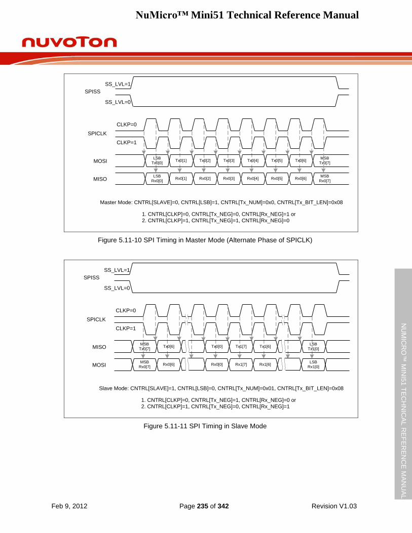
NuMicro™ Mini51 Technical Reference Manual
Feb 9, 2012 Page 235 of 342 Revision V1.03
NU
MIC
RO
™ M
INI5
1 T
EC
HN
ICA
L R
EF
ER
EN
CE
MA
NU
AL
SPICLK
MISO
Master Mode: CNTRL[SLAVE]=0, CNTRL[LSB]=1, CNTRL[Tx_NUM]=0x0, CNTRL[Tx_BIT_LEN]=0x08
MOSI Tx0[1] Tx0[2] Tx0[3] Tx0[4] Tx0[5] Tx0[6]MSB
Tx0[7]
LSB
Tx0[0]
CLKP=0
CLKP=1
SPISS
SS_LVL=1
SS_LVL=0
1. CNTRL[CLKP]=0, CNTRL[Tx_NEG]=0, CNTRL[Rx_NEG]=1 or
2. CNTRL[CLKP]=1, CNTRL[Tx_NEG]=1, CNTRL[Rx_NEG]=0
Rx0[1] Rx0[2] Rx0[3] Rx0[4] Rx0[5] Rx0[6]MSB
Rx0[7]
LSB
Rx0[0]
Figure 5.11-10 SPI Timing in Master Mode (Alternate Phase of SPICLK)
SPICLK
MOSI
Slave Mode: CNTRL[SLAVE]=1, CNTRL[LSB]=0, CNTRL[Tx_NUM]=0x01, CNTRL[Tx_BIT_LEN]=0x08
MISO Tx0[6] Tx0[0] Tx1[7] Tx1[6]LSB
Tx1[0]
MSB
Tx0[7]
Rx0[6] Rx0[0] Rx1[7] Rx1[6]LSB
Rx1[0]
MSB
Rx0[7]
CLKP=0
CLKP=1
SPISS
SS_LVL=1
SS_LVL=0
1. CNTRL[CLKP]=0, CNTRL[Tx_NEG]=1, CNTRL[Rx_NEG]=0 or
2. CNTRL[CLKP]=1, CNTRL[Tx_NEG]=0, CNTRL[Rx_NEG]=1
Figure 5.11-11 SPI Timing in Slave Mode
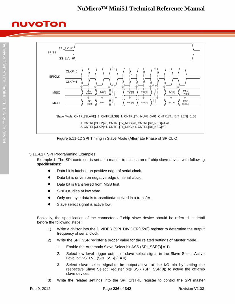
NuMicro™ Mini51 Technical Reference Manual
Feb 9, 2012 Page 236 of 342 Revision V1.03
NU
MIC
RO
™ M
INI5
1 T
EC
HN
ICA
L R
EF
ER
EN
CE
MA
NU
AL
SPICLK
MOSI
Slave Mode: CNTRL[SLAVE]=1, CNTRL[LSB]=1, CNTRL[Tx_NUM]=0x01, CNTRL[Tx_BIT_LEN]=0x08
MISO Tx0[1] Tx0[7] Tx1[0] Tx1[6]MSB
Tx1[7]
LSB
Tx0[0]
CLKP=0
CLKP=1
SPISS
SS_LVL=1
SS_LVL=0
1. CNTRL[CLKP]=0, CNTRL[Tx_NEG]=0, CNTRL[Rx_NEG]=1 or
2. CNTRL[CLKP]=1, CNTRL[Tx_NEG]=1, CNTRL[Rx_NEG]=0
Rx0[1] Rx0[7] Rx1[0] Rx1[6]MSB
Rx1[7]
LSB
Rx0[0]
Figure 5.11-12 SPI Timing in Slave Mode (Alternate Phase of SPICLK)
5.11.4.17 SPI Programming Examples
Example 1: The SPI controller is set as a master to access an off-chip slave device with following specifications:
Data bit is latched on positive edge of serial clock.
Data bit is driven on negative edge of serial clock.
Data bit is transferred from MSB first.
SPICLK idles at low state.
Only one byte data is transmitted/received in a transfer.
Slave select signal is active low.
Basically, the specification of the connected off-chip slave device should be referred in detail before the following steps:
1) Write a divisor into the DIVIDER (SPI_DIVIDER[15:0]) register to determine the output frequency of serial clock.
2) Write the SPI_SSR register a proper value for the related settings of Master mode.
1. Enable the Automatic Slave Select bit ASS (SPI_SSR[3] = 1).
2. Select low level trigger output of slave select signal in the Slave Select Active Level bit SS_LVL (SPI_SSR[2] = 0).
3. Select slave select signal to be output active at the I/O pin by setting the respective Slave Select Register bits SSR (SPI_SSR[0]) to active the off-chip slave devices.
3) Write the related settings into the SPI_CNTRL register to control the SPI master
NuMicro™ Mini51 Technical Reference Manual
Feb 9, 2012 Page 237 of 342 Revision V1.03
NU
MIC
RO
™ M
INI5
1 T
EC
HN
ICA
L R
EF
ER
EN
CE
MA
NU
AL
actions.
1. Set this SPI controller as the master device in SLAVE bit (SPI_CNTRL[18] = 0).
2. Force the serial clock idle state at low in CLKP bit (SPI_CNTRL[11] = 0).
3. Select data transmitted at negative edge of serial clock in TX_NEG bit (SPI_CNTRL[2] = 1).
4. Select data latched at positive edge of serial clock in RX_NEG bit (SPI_CNTRL[1] = 0).
5. Set the bit length of word transfer as 8 bits in TX_BIT_LEN bit field (SPI_CNTRL[7:3] = 0x08).
6. Set word transfer in TX_NUM (SPI_CNTRL[9:8] = 0x0) only once.
7. Set MSB transfer first in LSB bit (SPI_CNTRL[10] = 0), and disregard the SP_CYCLE bit field (SPI_CNTRL[15:12]) due to it‟s not burst mode in this case.
4) If this SPI master will transmit (write) one byte data to the off-chip slave device, write the byte data that will be transmitted into the Tx0 (SPI_TX0[7:0]) register.
5) If this SPI master just only receives (reads) one byte data from the off-chip slave device, disregard what data will be transmitted and just write 0xFF into the SPI_TX0[7:0] register.
6) Enable the GO_BUSY bit (SPI_CNTRL[0] = 1) to start the data transfer at the SPI interface.
Waiting for SPI interrupt occurred (if the Interrupt Enable IE bit is set) or just polling the GO_BUSY bit till it be cleared to “0” by hardware automatically.--
7) Read out the received one byte data from Rx0 (SPI_RX0[7:0]) register.
8) Go to 4) to continue with another data transfer or set SSR to “0” to inactivate the off-chip slave devices.
Example 2: The SPI controller is set as a slave device that is controlled by an off-chip master device, and supposes the off-chip master device to access the on-chip SPI slave controller through the SPI interface with the following specifications:
Data bit is latched on positive edge of serial clock.
Data bit is driven on negative edge of serial clock.
Data bit is transferred from LSB first.
SPICLK idles at high state.
Only one byte data is transmitted/received in a transfer.
Slave select signal is high level trigger.
Basically, the specification of the connected off-chip master device should be referred in detail before the following steps,
1) Write the SPI_SSR register a proper value for the related settings of Slave mode.
Select high level and level trigger for the input of slave select signal by setting the Slave Select Active Level bit SS_LVL (SPI_SSR[2] = 1) and the Slave Select Level Trigger bit SS_LTRIG (SPI_SSR[4] = 1).
NuMicro™ Mini51 Technical Reference Manual
Feb 9, 2012 Page 238 of 342 Revision V1.03
NU
MIC
RO
™ M
INI5
1 T
EC
HN
ICA
L R
EF
ER
EN
CE
MA
NU
AL
2) Write the related settings into the SPI_CNTRL register to control this SPI slave actions.
1. Set this SPI controller as slave device in SLAVE bit (SPI_CNTRL[18] = 1).
2. Select the serial clock idle state at high in CLKP bit (SPI_CNTRL[11] = 1).
3. Select data transmitted at negative edge of serial clock in TX_NEG bit (SPI_CNTRL[2] = 1).
4. Select data latched at positive edge of serial clock in RX_NEG bit (SPI_CNTRL[1] = 0).
5. Set the bit length of word transfer as 8 bits in TX_BIT_LEN bit field (SPI_CNTRL[7:3] = 0x08).
6. Set only one time of word transfer in TX_NUM (SPI_CNTRL[9:8] = 0x0).
7. Set LSB transfer first in LSB bit (SPI_CNTRL[10] = 1), and disregard the SP_CYCLE bit field (SPI_CNTRL[15:12]) due to it‟s not burst mode in this case.
3) If this SPI slave will transmit (be read) one byte data to the off-chip master device, write the byte data that will be transmitted into the Tx0 (SPI_TX0[7:0]) register.
4) If this SPI slave just only receives (be written) one byte data from the off-chip master device, disregard what data will be transmitted and just write 0xFF into the SPI_TX0[7:0] register.
5) Enable the GO_BUSY bit (SPI_CNTRL[0] = 1) to wait for the slave select trigger input and serial clock input from the off-chip master device to start the data transfer at the SPI interface.
Waiting for SPI interrupt to occur (if the Interrupt Enable IE bit is set) or just polling the GO_BUSY bit until it is cleared to “0” by hardware automatically.
6) Read out the received one byte data from Rx (SPI_RX0[7:0]) register.
7) Go to 3) to continue with another data transfer or disable the GO_BUSY bit to stop data transfer.
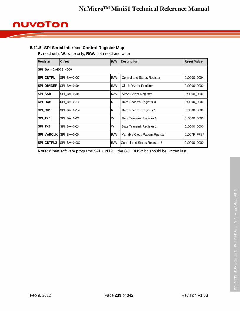
NuMicro™ Mini51 Technical Reference Manual
Feb 9, 2012 Page 239 of 342 Revision V1.03
NU
MIC
RO
™ M
INI5
1 T
EC
HN
ICA
L R
EF
ER
EN
CE
MA
NU
AL
5.11.5 SPI Serial Interface Control Register Map
R: read only, W: write only, R/W: both read and write
Register Offset R/W Description Reset Value
SPI_BA = 0x4003_4000
SPI_CNTRL SPI_BA+0x00 R/W Control and Status Register 0x0000_0004
SPI_DIVIDER SPI_BA+0x04 R/W Clock Divider Register 0x0000_0000
SPI_SSR SPI_BA+0x08 R/W Slave Select Register 0x0000_0000
SPI_RX0 SPI_BA+0x10 R Data Receive Register 0 0x0000_0000
SPI_RX1 SPI_BA+0x14 R Data Receive Register 1 0x0000_0000
SPI_TX0 SPI_BA+0x20 W Data Transmit Register 0 0x0000_0000
SPI_TX1 SPI_BA+0x24 W Data Transmit Register 1 0x0000_0000
SPI_VARCLK SPI_BA+0x34 R/W Variable Clock Pattern Register 0x007F_FF87
SPI_CNTRL2 SPI_BA+0x3C R/W Control and Status Register 2 0x0000_0000
Note: When software programs SPI_CNTRL, the GO_BUSY bit should be written last.
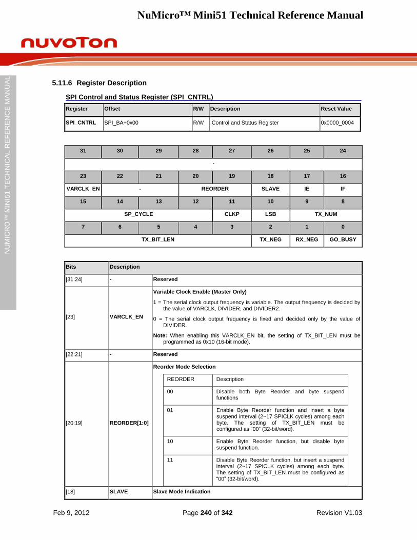
NuMicro™ Mini51 Technical Reference Manual
Feb 9, 2012 Page 240 of 342 Revision V1.03
NU
MIC
RO
™ M
INI5
1 T
EC
HN
ICA
L R
EF
ER
EN
CE
MA
NU
AL
5.11.6 Register Description
SPI Control and Status Register (SPI_CNTRL)
Register Offset R/W Description Reset Value
SPI_CNTRL SPI_BA+0x00 R/W Control and Status Register 0x0000_0004
31 30 29 28 27 26 25 24
-
23 22 21 20 19 18 17 16
VARCLK_EN - REORDER SLAVE IE IF
15 14 13 12 11 10 9 8
SP_CYCLE CLKP LSB TX_NUM
7 6 5 4 3 2 1 0
TX_BIT_LEN TX_NEG RX_NEG GO_BUSY
Bits Description
[31:24] - Reserved
[23] VARCLK_EN
Variable Clock Enable (Master Only)
1 = The serial clock output frequency is variable. The output frequency is decided by the value of VARCLK, DIVIDER, and DIVIDER2.
0 = The serial clock output frequency is fixed and decided only by the value of DIVIDER.
Note: When enabling this VARCLK_EN bit, the setting of TX_BIT_LEN must be programmed as 0x10 (16-bit mode).
[22:21] - Reserved
[20:19] REORDER[1:0]
Reorder Mode Selection
REORDER Description
00 Disable both Byte Reorder and byte suspend functions
01 Enable Byte Reorder function and insert a byte suspend interval (2~17 SPICLK cycles) among each byte. The setting of TX_BIT_LEN must be configured as “00” (32-bit/word).
10 Enable Byte Reorder function, but disable byte suspend function.
11 Disable Byte Reorder function, but insert a suspend interval (2~17 SPICLK cycles) among each byte. The setting of TX_BIT_LEN must be configured as “00” (32-bit/word).
[18] SLAVE Slave Mode Indication
NuMicro™ Mini51 Technical Reference Manual
Feb 9, 2012 Page 241 of 342 Revision V1.03
NU
MIC
RO
™ M
INI5
1 T
EC
HN
ICA
L R
EF
ER
EN
CE
MA
NU
AL
Bits Description
1 = Slave mode.
0 = Master mode.
[17] IE
Interrupt Enable
1 = SPI Interrupt Enabled.
0 = SPI Interrupt Disabled.
[16] IF
Interrupt Flag
1 = The transfer done. The interrupt flag is set if it was enabled.
0 =The transfer does not finish yet.
Note: This bit is cleared by writing “1” to itself.
[15:12] SP_CYCLE[3:0]
Suspend Interval (Master Only)
The four bits provide configurable suspend interval between two successive transmit/receive transaction in a transfer. The suspend interval is from the last falling clock edge of the current transaction to the first rising clock edge of the successive transaction if CLKP = 0. If CLKP = 1, the interval is from the rising clock edge to the falling clock edge. The default value is “0”. When TX_NUM = 00, setting this field has no effect on transfer. The desired suspend interval is obtained according to the following equation:
(SP_CYCLE[3:0] + 2) * period of SPICLK
SP_CYCLE Value The suspend Interval
0000 2 SPICLK clock cycle
0001 3 SPICLK clock cycle
------ ----------
1110 16 SPICLK clock cycle
1111 17 SPICLK clock cycle
[11] CLKP
Clock Polarity
1 = SPICLK idle high.
0 = SPICLK idle low.
[10] LSB
LSB First
1 = The LSB sent first on the line (bit 0 of SPI_TX0/1), and the first bit received from the line will be put in the LSB position in the Rx register (bit 0 of SPI_RX0/1).
0 = The MSB transmitted/received first (which bit in SPI_TX0/1 and SPI_RX0/1 register depends on the TX_BIT_LEN field).
[9:8] TX_NUM[1:0]
Transmit/Receive Word Numbers
This field specifies how many transmit/receive word numbers should be executed in one transfer.
TX_NUM Description
00 Only one transmit/receive transaction will be executed in one transfer.
01 Two successive transmit/receive transactions will be executed in one transfer (burst mode).
10 Reserved
NuMicro™ Mini51 Technical Reference Manual
Feb 9, 2012 Page 242 of 342 Revision V1.03
NU
MIC
RO
™ M
INI5
1 T
EC
HN
ICA
L R
EF
ER
EN
CE
MA
NU
AL
Bits Description
11 Reserved
Note: In Slave mode with level-trigger configuration, the slave select pin must be kept at active state during the successive data transfer.
[7:3] TX_BIT_LEN [4:0]
Transmit Bit Length
This field specifies how many bits are transmitted in one transmit/receive. Up to 32 bits can be transmitted.
TX_BIT_LEN Description
00001 1 bit is transmitted in one transaction
00010 2 bits are transmitted in one transaction
00011 3 bits are transmitted in one transaction
------ ----------
11111 31 bits are transmitted in one transaction
00000 32 bits are transmitted in one transaction
[2] TX_NEG
Transmit At Negative Edge
1 = The transmitted data output signal changed at the falling edge of SPICLK.
0 = The transmitted data output signal changed at the rising edge of SPICLK.
[1] RX_NEG
Receive At Negative Edge
1 = The received data input signal latched at the falling edge of SPICLK.
0 = The received data input signal latched at the rising edge of SPICLK.
[0] GO_BUSY
Go and Busy Status
1= In Master mode, writing “1” to this bit to start the SPI data transfer; in Slave mode, writing “1” to this bit indicates that the slave is ready to communicate with a master. During the data transfer, this bit keeps the value of “1”. As the transfer is finished, this bit will be cleared automatically.
0 = Data transfer stopped if SPI is transferring.
Note: All registers should be set before writing “1” to the GO_BUSY bit.
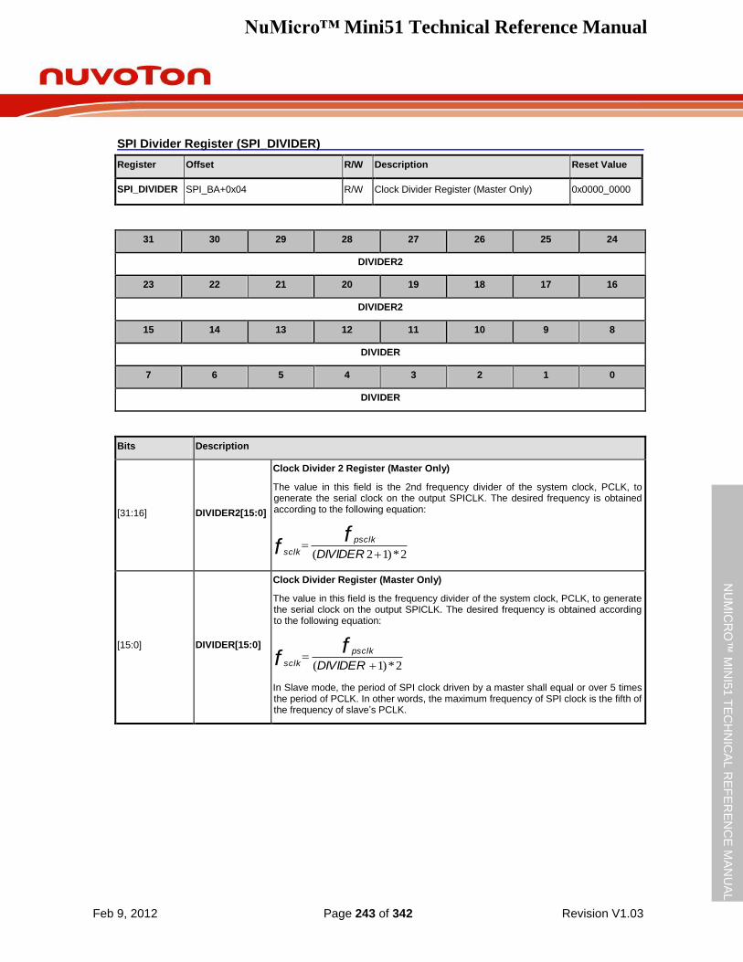
NuMicro™ Mini51 Technical Reference Manual
Feb 9, 2012 Page 243 of 342 Revision V1.03
NU
MIC
RO
™ M
INI5
1 T
EC
HN
ICA
L R
EF
ER
EN
CE
MA
NU
AL
SPI Divider Register (SPI_DIVIDER)
Register Offset R/W Description Reset Value
SPI_DIVIDER SPI_BA+0x04 R/W Clock Divider Register (Master Only) 0x0000_0000
31 30 29 28 27 26 25 24
DIVIDER2
23 22 21 20 19 18 17 16
DIVIDER2
15 14 13 12 11 10 9 8
DIVIDER
7 6 5 4 3 2 1 0
DIVIDER
Bits Description
[31:16] DIVIDER2[15:0]
Clock Divider 2 Register (Master Only)
The value in this field is the 2nd frequency divider of the system clock, PCLK, to generate the serial clock on the output SPICLK. The desired frequency is obtained according to the following equation:
2*)12(
DIVIDER
ff
psclk
sclk
[15:0] DIVIDER[15:0]
Clock Divider Register (Master Only)
The value in this field is the frequency divider of the system clock, PCLK, to generate the serial clock on the output SPICLK. The desired frequency is obtained according to the following equation:
2*)1(
DIVIDER
ff
psclk
sclk
In Slave mode, the period of SPI clock driven by a master shall equal or over 5 times the period of PCLK. In other words, the maximum frequency of SPI clock is the fifth of the frequency of slave‟s PCLK.
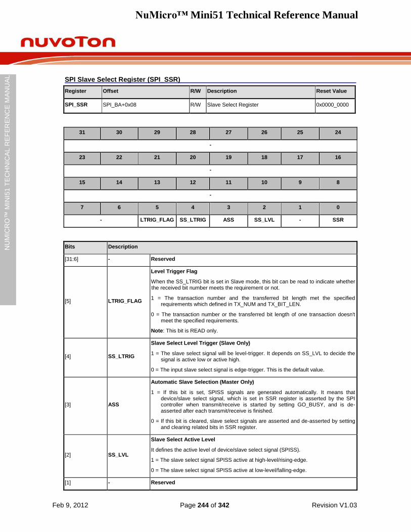
NuMicro™ Mini51 Technical Reference Manual
Feb 9, 2012 Page 244 of 342 Revision V1.03
NU
MIC
RO
™ M
INI5
1 T
EC
HN
ICA
L R
EF
ER
EN
CE
MA
NU
AL
SPI Slave Select Register (SPI_SSR)
Register Offset R/W Description Reset Value
SPI_SSR SPI_BA+0x08 R/W Slave Select Register 0x0000_0000
31 30 29 28 27 26 25 24
-
23 22 21 20 19 18 17 16
-
15 14 13 12 11 10 9 8
-
7 6 5 4 3 2 1 0
- LTRIG_FLAG SS_LTRIG ASS SS_LVL - SSR
Bits Description
[31:6] - Reserved
[5] LTRIG_FLAG
Level Trigger Flag
When the SS_LTRIG bit is set in Slave mode, this bit can be read to indicate whether the received bit number meets the requirement or not.
1 = The transaction number and the transferred bit length met the specified requirements which defined in TX_NUM and TX_BIT_LEN.
0 = The transaction number or the transferred bit length of one transaction doesn't meet the specified requirements.
Note: This bit is READ only.
[4] SS_LTRIG
Slave Select Level Trigger (Slave Only)
1 = The slave select signal will be level-trigger. It depends on SS_LVL to decide the signal is active low or active high.
0 = The input slave select signal is edge-trigger. This is the default value.
[3] ASS
Automatic Slave Selection (Master Only)
1 = If this bit is set, SPISS signals are generated automatically. It means that device/slave select signal, which is set in SSR register is asserted by the SPI controller when transmit/receive is started by setting GO_BUSY, and is de-asserted after each transmit/receive is finished.
0 = If this bit is cleared, slave select signals are asserted and de-asserted by setting and clearing related bits in SSR register.
[2] SS_LVL
Slave Select Active Level
It defines the active level of device/slave select signal (SPISS).
1 = The slave select signal SPISS active at high-level/rising-edge.
0 = The slave select signal SPISS active at low-level/falling-edge.
[1] - Reserved
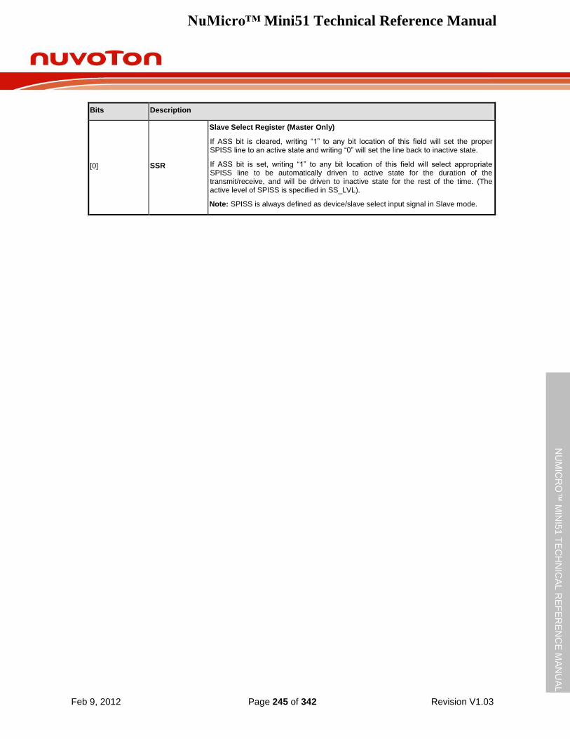
NuMicro™ Mini51 Technical Reference Manual
Feb 9, 2012 Page 245 of 342 Revision V1.03
NU
MIC
RO
™ M
INI5
1 T
EC
HN
ICA
L R
EF
ER
EN
CE
MA
NU
AL
Bits Description
[0] SSR
Slave Select Register (Master Only)
If ASS bit is cleared, writing “1” to any bit location of this field will set the proper SPISS line to an active state and writing “0” will set the line back to inactive state.
If ASS bit is set, writing “1” to any bit location of this field will select appropriate SPISS line to be automatically driven to active state for the duration of the transmit/receive, and will be driven to inactive state for the rest of the time. (The active level of SPISS is specified in SS_LVL).
Note: SPISS is always defined as device/slave select input signal in Slave mode.
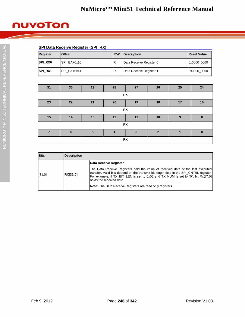
NuMicro™ Mini51 Technical Reference Manual
Feb 9, 2012 Page 246 of 342 Revision V1.03
NU
MIC
RO
™ M
INI5
1 T
EC
HN
ICA
L R
EF
ER
EN
CE
MA
NU
AL
SPI Data Receive Register (SPI_RX)
Register Offset R/W Description Reset Value
SPI_RX0 SPI_BA+0x10 R Data Receive Register 0 0x0000_0000
SPI_RX1 SPI_BA+0x14 R Data Receive Register 1 0x0000_0000
31 30 29 28 27 26 25 24
RX
23 22 21 20 19 18 17 16
RX
15 14 13 12 11 10 9 8
RX
7 6 5 4 3 2 1 0
RX
Bits Description
[31:0] RX[31:0]
Data Receive Register
The Data Receive Registers hold the value of received data of the last executed transfer. Valid bits depend on the transmit bit length field in the SPI_CNTRL register. For example, if TX_BIT_LEN is set to 0x08 and TX_NUM is set to “0”, bit Rx0[7:0] holds the received data.
Note: The Data Receive Registers are read only registers.
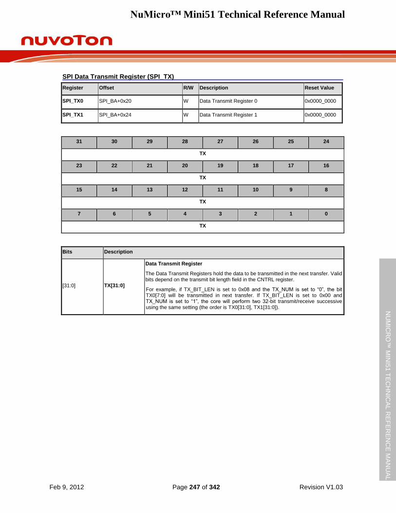
NuMicro™ Mini51 Technical Reference Manual
Feb 9, 2012 Page 247 of 342 Revision V1.03
NU
MIC
RO
™ M
INI5
1 T
EC
HN
ICA
L R
EF
ER
EN
CE
MA
NU
AL
SPI Data Transmit Register (SPI_TX)
Register Offset R/W Description Reset Value
SPI_TX0 SPI_BA+0x20 W Data Transmit Register 0 0x0000_0000
SPI_TX1 SPI_BA+0x24 W Data Transmit Register 1 0x0000_0000
31 30 29 28 27 26 25 24
TX
23 22 21 20 19 18 17 16
TX
15 14 13 12 11 10 9 8
TX
7 6 5 4 3 2 1 0
TX
Bits Description
[31:0] TX[31:0]
Data Transmit Register
The Data Transmit Registers hold the data to be transmitted in the next transfer. Valid bits depend on the transmit bit length field in the CNTRL register.
For example, if TX_BIT_LEN is set to 0x08 and the TX_NUM is set to “0”, the bit TX0[7:0] will be transmitted in next transfer. If TX_BIT_LEN is set to 0x00 and TX_NUM is set to “1”, the core will perform two 32-bit transmit/receive successive using the same setting (the order is TX0[31:0], TX1[31:0]).
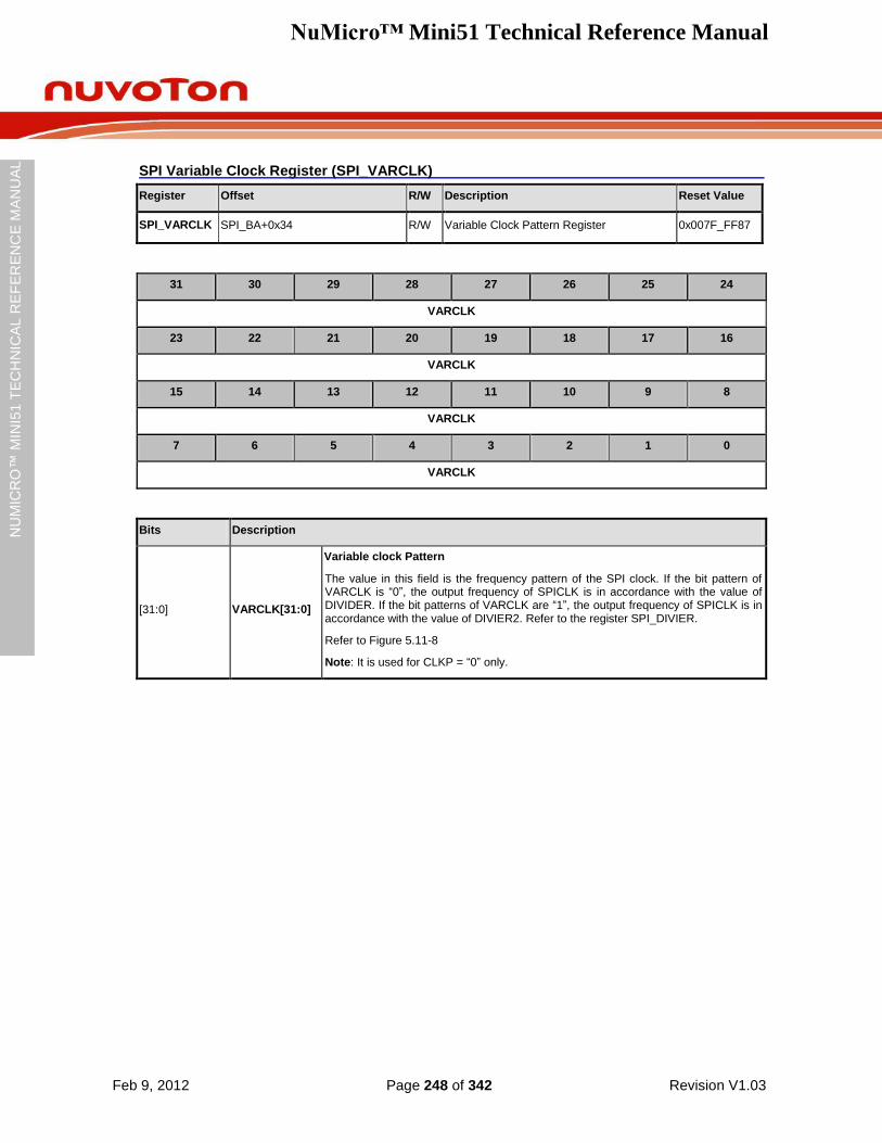
NuMicro™ Mini51 Technical Reference Manual
Feb 9, 2012 Page 248 of 342 Revision V1.03
NU
MIC
RO
™ M
INI5
1 T
EC
HN
ICA
L R
EF
ER
EN
CE
MA
NU
AL
SPI Variable Clock Register (SPI_VARCLK)
Register Offset R/W Description Reset Value
SPI_VARCLK SPI_BA+0x34 R/W Variable Clock Pattern Register 0x007F_FF87
31 30 29 28 27 26 25 24
VARCLK
23 22 21 20 19 18 17 16
VARCLK
15 14 13 12 11 10 9 8
VARCLK
7 6 5 4 3 2 1 0
VARCLK
Bits Description
[31:0] VARCLK[31:0]
Variable clock Pattern
The value in this field is the frequency pattern of the SPI clock. If the bit pattern of VARCLK is “0”, the output frequency of SPICLK is in accordance with the value of DIVIDER. If the bit patterns of VARCLK are “1”, the output frequency of SPICLK is in accordance with the value of DIVIER2. Refer to the register SPI_DIVIER.
Refer to Figure 5.11-8
Note: It is used for CLKP = “0” only.
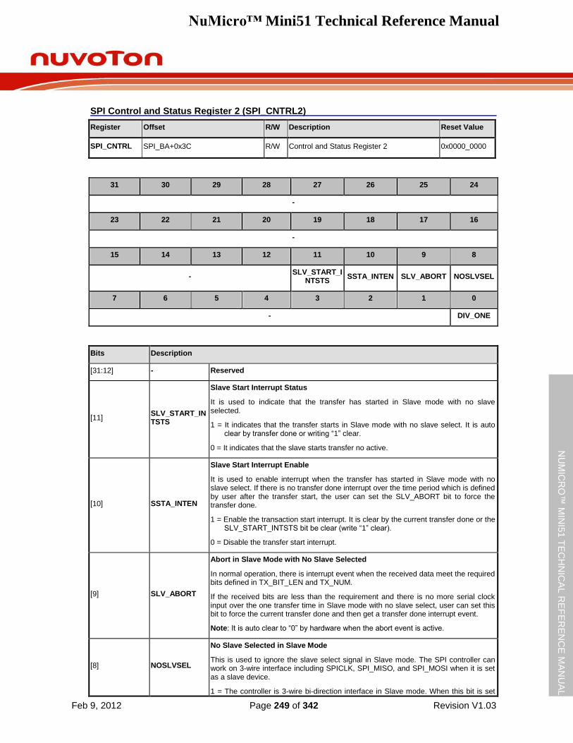
NuMicro™ Mini51 Technical Reference Manual
Feb 9, 2012 Page 249 of 342 Revision V1.03
NU
MIC
RO
™ M
INI5
1 T
EC
HN
ICA
L R
EF
ER
EN
CE
MA
NU
AL
SPI Control and Status Register 2 (SPI_CNTRL2)
Register Offset R/W Description Reset Value
SPI_CNTRL SPI_BA+0x3C R/W Control and Status Register 2 0x0000_0000
31 30 29 28 27 26 25 24
-
23 22 21 20 19 18 17 16
-
15 14 13 12 11 10 9 8
- SLV_START_I
NTSTS SSTA_INTEN SLV_ABORT NOSLVSEL
7 6 5 4 3 2 1 0
- DIV_ONE
Bits Description
[31:12] - Reserved
[11] SLV_START_INTSTS
Slave Start Interrupt Status
It is used to indicate that the transfer has started in Slave mode with no slave selected.
1 = It indicates that the transfer starts in Slave mode with no slave select. It is auto clear by transfer done or writing “1” clear.
0 = It indicates that the slave starts transfer no active.
[10] SSTA_INTEN
Slave Start Interrupt Enable
It is used to enable interrupt when the transfer has started in Slave mode with no slave select. If there is no transfer done interrupt over the time period which is defined by user after the transfer start, the user can set the SLV_ABORT bit to force the transfer done.
1 = Enable the transaction start interrupt. It is clear by the current transfer done or the SLV_START_INTSTS bit be clear (write “1” clear).
0 = Disable the transfer start interrupt.
[9] SLV_ABORT
Abort in Slave Mode with No Slave Selected
In normal operation, there is interrupt event when the received data meet the required bits defined in TX_BIT_LEN and TX_NUM.
If the received bits are less than the requirement and there is no more serial clock input over the one transfer time in Slave mode with no slave select, user can set this bit to force the current transfer done and then get a transfer done interrupt event.
Note: It is auto clear to “0” by hardware when the abort event is active.
[8] NOSLVSEL
No Slave Selected in Slave Mode
This is used to ignore the slave select signal in Slave mode. The SPI controller can work on 3-wire interface including SPICLK, SPI_MISO, and SPI_MOSI when it is set as a slave device.
1 = The controller is 3-wire bi-direction interface in Slave mode. When this bit is set
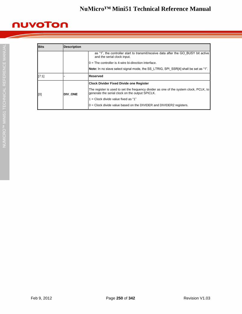
NuMicro™ Mini51 Technical Reference Manual
Feb 9, 2012 Page 250 of 342 Revision V1.03
NU
MIC
RO
™ M
INI5
1 T
EC
HN
ICA
L R
EF
ER
EN
CE
MA
NU
AL
Bits Description
as “1”, the controller start to transmit/receive data after the GO_BUSY bit active and the serial clock input.
0 = The controller is 4-wire bi-direction interface.
Note: In no slave select signal mode, the SS_LTRIG, SPI_SSR[4] shall be set as “1”.
[7:1] - Reserved
[0] DIV_ONE
Clock Divider Fixed Divide one Register
The register is used to set the frequency divider as one of the system clock, PCLK, to generate the serial clock on the output SPICLK.
1 = Clock divide value fixed as “1”
0 = Clock divide value based on the DIVIDER and DIVIDER2 registers.

NuMicro™ Mini51 Technical Reference Manual
Feb 9, 2012 Page 251 of 342 Revision V1.03
NU
MIC
RO
™ M
INI5
1 T
EC
HN
ICA
L R
EF
ER
EN
CE
MA
NU
AL
5.12 Timer Controller
5.12.1 Overview
The timer module includes two channels, TIMER0~TIMER1, which allow user to easily implement a timer control for applications. The timer can perform functions like frequency measurement, interval measurement, clock generation, delay timing, and so on. The timer can generate an interrupt signal upon time-out, or provide the current value of count during operation.
5.12.2 Features
Two sets of 32-bit timers with 24-bit up-timer and one 8-bit pre-scale counter
Independent clock source for each channel (TMR0_CLK, TMR1_CLK)
Provides one-shot, periodic, toggle and continuous counting operation modes
Time-out period = (period of timer clock input) * (8-bit pre-scale counter + 1) * (24-bit TCMP)
Maximum counting cycle time = (1 / T MHz) * (28) * (2
24); T is the period of timer clock
Internal 24-bit up timer is readable through TDR (Timer Data Register)
Supports event counting function to count the event from external pin
Supports input capture function to capture or reset counter value
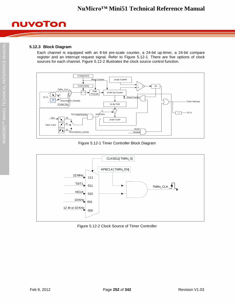
NuMicro™ Mini51 Technical Reference Manual
Feb 9, 2012 Page 252 of 342 Revision V1.03
NU
MIC
RO
™ M
INI5
1 T
EC
HN
ICA
L R
EF
ER
EN
CE
MA
NU
AL
5.12.3 Block Diagram
Each channel is equipped with an 8-bit pre-scale counter, a 24-bit up-timer, a 24-bit compare register and an interrupt request signal. Refer to Figure 5.12-1. There are five options of clock sources for each channel. Figure 5.12-2 illustrates the clock source control function.
Reset Counter
+-
= TIF
Timer Interrupt
0
1
TCSR[CRST]
TCSR [CEN]
24-Bit TCMPR
8-Bit
Prescale24-Bit Up-Counter
Reset Counter
24-Bit TDR
24-Bit TCAP
TEXIF
TEXIEN
TMRx_CLK
T0-T1
TEX
T0EX-T1EX
00
01
10
TEXCON[TEX_EDGE]
TEXCON[TEXEN]
0
1
RSTCAPn
0
1
TCSR[CTB]
TEXCON[TX_PHASE]
÷ 2 T0-T1
Figure 5.12-1 Timer Controller Block Diagram
22 MHz
T0/T1
HCLK
10 KHz
12 M or 32 KHz
111
011
010
001
000
TMRx_CLK
CLKSEL1[ TMRx_S]
APBCLK[ TMRx_EN]
Figure 5.12-2 Clock Source of Timer Controller
NuMicro™ Mini51 Technical Reference Manual
Feb 9, 2012 Page 253 of 342 Revision V1.03
NU
MIC
RO
™ M
INI5
1 T
EC
HN
ICA
L R
EF
ER
EN
CE
MA
NU
AL
5.12.4 Functional Description
A Timer controller provides one-shot, periodic, toggle and continuous counting operation modes. It also provides the event counting function to count the event from the external pin and input capture function to capture or reset timer counter value. Each operating function mode is shown as follows:
5.12.4.1 One-Shot Mode
If the timer is operated at one-shot mode and CEN (TCSR[30] timer enable bit) is set to “1”, the timer counter starts up counting. Once the timer counter value reaches timer compare register (TCMPR) value, if IE (TCSR[29] interrupt enable bit) is set to “1”, then the timer interrupt flag is set and the interrupt signal is generated and sent to NVIC to inform CPU. It indicates that the timer counting overflow happens. If IE is set to “0”, no interrupt signal is generated. In this operation mode, once the timer counter value reaches timer compare register (TCMPR) value, the timer counter value goes back to counting initial value and CEN is cleared to “0” by timer controller. Timer counting operation stops, once the timer counter value reaches timer compare register (TCMPR) value. That is to say, timer operates timer counting and compares with TCMPR value function only one time after programming the timer compare register (TCMPR) value and CEN is set to “1”. So, this operation mode is called One-Shot mode.
5.12.4.2 Periodic Mode
If the timer is operated at period mode and CEN is set to “1”, the timer counter starts up counting. Once the timer counter value reaches timer compare register (TCMPR) value, if IE is set to “1”, then the timer interrupt flag is set and the interrupt signal is generated and sent to NVIC to inform CPU. It indicates that the timer counting overflow happens. If IE is set to “0”, no interrupt signal is generated. In this operation mode, once the timer counter value reaches timer compare register (TCMPR) value, the timer counter value goes back to counting initial value and CEN is kept at “1” (counting enable continuously). The timer counter operates up counting again. If the interrupt flag is cleared by software, once the timer counter value reaches timer compare register (TCMPR) value and IE is set to “1”, then the timer interrupt flag is set and the interrupt signal is generated and sent to NVIC to inform CPU again. That is to say, timer operates timer counting and compares with TCMPR value function periodically. The timer counting operation doesn‟t stop until the CEN is set to “0”. The interrupt signal is also generated periodically. So, this operation mode is called Periodic mode.
5.12.4.3 Toggle Mode
If the timer is operated at toggle mode and CEN is set to “1”, the timer counter starts up counting. Once the timer counter value reaches timer compare register (TCMPR) value, if IE is set to “1”, then the timer interrupt flag is set and the interrupt signal is generated and sent to NVIC to inform CPU. It indicates that the timer counting overflow happens. The associated toggle output (tout) signal is set to “1”. In this operation mode, once the timer counter value reaches timer compare register (TCMPR) value, the timer counter value goes back to counting initial value and CEN is kept at “1” (counting enable continuously). The timer counter operates up counting again. If the interrupt flag is cleared by software, once the timer counter value reaches timer compare register (TCMPR) value and IE is set to “1”, then the timer interrupt flag is set and the interrupt signal is generated and sent to NVIC to inform CPU again. The associated toggle output (tout) signal is set to “0”. The timer counting operation doesn‟t stop until the CEN is set to “0”. Thus, the toggle output (tout) signal is changing back and force with 50% duty cycle. So, this operation mode is called Toggle mode.
5.12.4.4 Continuous Counting Mode
If the timer is operated at continuous counting mode and CEN is set to “1”, the associated interrupt
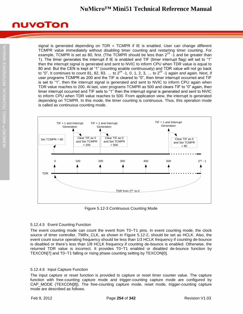
NuMicro™ Mini51 Technical Reference Manual
Feb 9, 2012 Page 254 of 342 Revision V1.03
NU
MIC
RO
™ M
INI5
1 T
EC
HN
ICA
L R
EF
ER
EN
CE
MA
NU
AL
signal is generated depending on TDR = TCMPR if IE is enabled. User can change different TCMPR value immediately without disabling timer counting and restarting timer counting. For example, TCMPR is set as 80, first. (The TCMPR should be less than 2
24 -1 and be greater than
1). The timer generates the interrupt if IE is enabled and TIF (timer interrupt flag) will set to “1” then the interrupt signal is generated and sent to NVIC to inform CPU when TDR value is equal to 80 and. But the CEN is kept at “1” (counting enable continuously) and TDR value will not go back to “0”, It continues to count 81, 82, 83, … to 2
24 -1, 0, 1, 2, 3, … to 2
24 -1 again and again. Next, if
user programs TCMPR as 200 and the TIF is cleared to “0”, then timer interrupt occurred and TIF is set to “1”, then the interrupt signal is generated and sent to NVIC to inform CPU again when TDR value reaches to 200. At last, user programs TCMPR as 500 and clears TIF to “0” again, then timer interrupt occurred and TIF sets to “1” then the interrupt signal is generated and sent to NVIC to inform CPU when TDR value reaches to 500. From application view, the interrupt is generated depending on TCMPR. In this mode, the timer counting is continuous. Thus, this operation mode is called as continuous counting mode.
0
TIF = 1 and Interrupt
Generation
TIF = 1 and Interrupt
Generation
TIF = 1 and Interrupt
Generation
Set TCMPR = 80
TDR
100 200 300 400 500 224 - 1
TDR from 224 to 0
Clear TIF as 0
and Set TCMPR
= 200
Clear TIF as 0
and Set TCMPR
= 500
Clear TIF as 0
and Set TCMPR
= 80
Figure 5.12-3 Continuous Counting Mode
5.12.4.5 Event Counting Function
The event counting mode can count the event from T0~T1 pins. In event counting mode, the clock source of timer controller, TMRx_CLK, as shown in Figure 5.12-2, should be set as HCLK. Also, the event count source operating frequency should be less than 1/3 HCLK frequency if counting de-bounce is disabled or there‟s less than 1/8 HCLK frequency if counting de-bounce is enabled. Otherwise, the returned TDR value is incorrect. It provides T0~T1 enabled or disabled de-bounce function by TEXCON[7] and T0~T1 falling or rising phase counting setting by TEXCON[0].
5.12.4.6 Input Capture Function
The input capture or reset function is provided to capture or reset timer counter value. The capture function with free-counting capture mode and trigger-counting capture mode are configured by CAP_MODE (TEXCON[8]). The free-counting capture mode, reset mode, trigger-counting capture mode are described as follows.
NuMicro™ Mini51 Technical Reference Manual
Feb 9, 2012 Page 255 of 342 Revision V1.03
NU
MIC
RO
™ M
INI5
1 T
EC
HN
ICA
L R
EF
ER
EN
CE
MA
NU
AL
5.12.4.7 Free-Counting Capture Mode
If CAP_MODE is cleared to “0”, TEXEN (TEXCON[3]) is set to “1” and RSTCAPN is set to “0”, the TDR will be captured into TCAP register when TEX (Timer External Pin) pin trigger condition occurred. The TEX trigger edge can be chosen by TEX_EDGE. The detail operation method is described in.
5.12.4.8 Reset Mode
If CAP_MODE is cleared to “0”, TEXEN (TEXCON[3]) is set to “1” and RSTCAPN is set to “1”, the TDR will be reset to “0” when TEX pin trigger condition happened. The TEX trigger edge can be chosen by TEX_EDGE. The detail operation method is described in.
5.12.4.9 Trigger-Counting Capture Mode
If CAP_MODE is set to “1”, TEXEN (TEXCON[3]) is set to “1” and RSTCAPN is set to “0”, the TDR will be reset to “0” then captured into TCAP register when TEX (Timer External Pin) pin trigger condition occurred. The TEX trigger edge can be chosen by TEX_EDGE. The detailed operation method is described.
When TEX trigger occurred, TEXIF (Timer External Interrupt Flag) is set to “1”, and the interrupt signal is generated, then, sent to NVIC to inform CPU if TEXIEN (Timer External Interrupt Enable Bit) is “1”. Also, the TEX source operating frequency should be less than 1/3 HCLK frequency if disable TEX de-bounce or less than 1/8 HCLK frequency if enabling TEX de-bounce. It also provides T0EX~T1EX enabled or disabled capture de-bounce function by TEXCON[6].
Table 5.12-1 Input Capture Mode Operation
Function CAP_MODE
(TEXCON[8])
RSTCAPN
(TEXCON[4])
TEX_EDGE
(TEXCON[2:1]) Operation Description
Free-counting Capture Mode
0 0 00 The high to zero transition on Timer External Input Pin is detected. TDR is captured to TCAP.
0 0 01 The zero to high transition on Timer External Input Pin is detected. TDR is captured to TCAP.
0 0 10 Either high to zero or zero to high transition on Timer External Input Pin is detected. TDR is captured to TCAP.
0 0 11 Reserved
Reset Mode
0 1 00 The high to zero transition on Timer External Input Pin is detected. TDR is reset to “0”.
0 1 01 The zero to high transition on Timer External Input Pin is detected. TDR is reset to “0”.
0 1 10 Either high to zero or zero to high transition on Timer External Input Pin is detected. TDR is reset to “0”.
0 1 11 Reserved
Trigger-Counting
1 0 00 Falling Edge Trigger:
The 1st high to zero transition on Timer
NuMicro™ Mini51 Technical Reference Manual
Feb 9, 2012 Page 256 of 342 Revision V1.03
NU
MIC
RO
™ M
INI5
1 T
EC
HN
ICA
L R
EF
ER
EN
CE
MA
NU
AL
Capture Mode External Input Pin is detected to reset TDR as “0” and then starts counting, while the 2nd high to zero transition stops counting
1 0 01
Rising Edge Trigger:
The 1st zero to high transition on Timer External Input Pin is detected to reset TDR as “0” and then starts counting, while the 2nd zero to high transition stops counting.
1 0 10
Level Change Trigger:
The high to zero transition on Timer External Input Pin is detected to reset TDR as “0” and then starts counting, while zero to high transition stops counting.
1 0 11
Level Change Trigger:
The zero to high transition on Timer External Input Pin is detected to reset TDR as “0” and then starts counting, while high to zero transition stops counting.
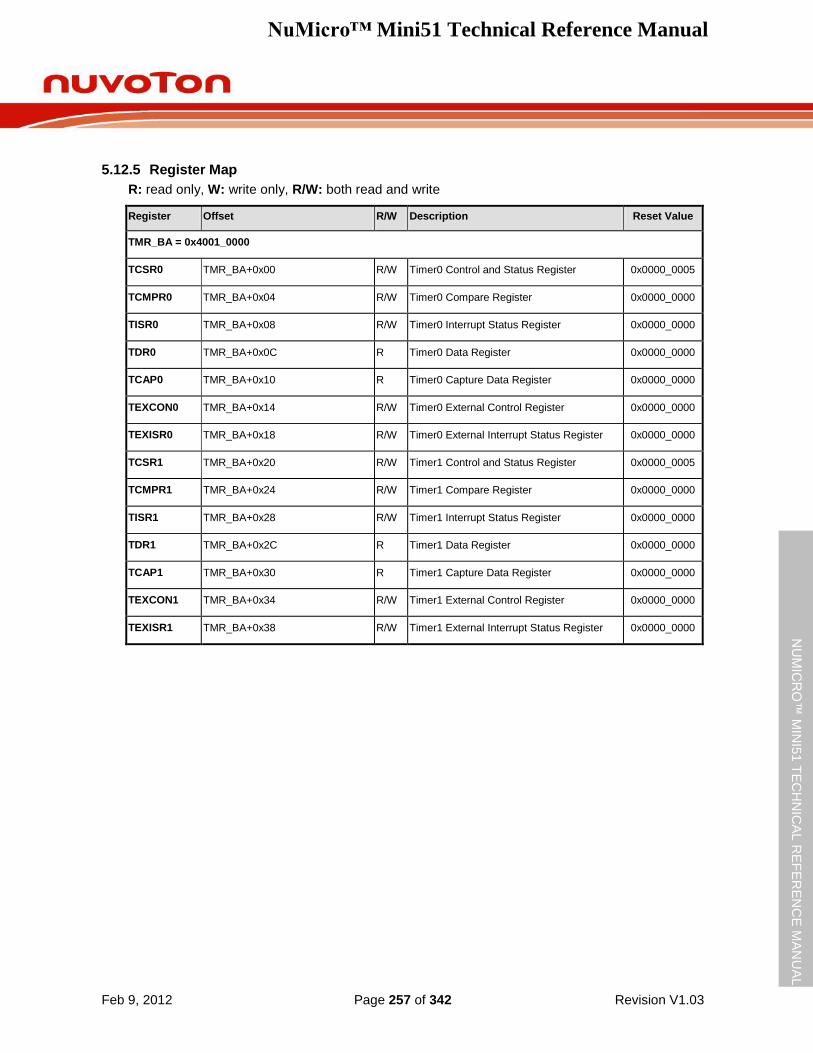
NuMicro™ Mini51 Technical Reference Manual
Feb 9, 2012 Page 257 of 342 Revision V1.03
NU
MIC
RO
™ M
INI5
1 T
EC
HN
ICA
L R
EF
ER
EN
CE
MA
NU
AL
5.12.5 Register Map
R: read only, W: write only, R/W: both read and write
Register Offset R/W Description Reset Value
TMR_BA = 0x4001_0000
TCSR0 TMR_BA+0x00 R/W Timer0 Control and Status Register 0x0000_0005
TCMPR0 TMR_BA+0x04 R/W Timer0 Compare Register 0x0000_0000
TISR0 TMR_BA+0x08 R/W Timer0 Interrupt Status Register 0x0000_0000
TDR0 TMR_BA+0x0C R Timer0 Data Register 0x0000_0000
TCAP0 TMR_BA+0x10 R Timer0 Capture Data Register 0x0000_0000
TEXCON0 TMR_BA+0x14 R/W Timer0 External Control Register 0x0000_0000
TEXISR0 TMR_BA+0x18 R/W Timer0 External Interrupt Status Register 0x0000_0000
TCSR1 TMR_BA+0x20 R/W Timer1 Control and Status Register 0x0000_0005
TCMPR1 TMR_BA+0x24 R/W Timer1 Compare Register 0x0000_0000
TISR1 TMR_BA+0x28 R/W Timer1 Interrupt Status Register 0x0000_0000
TDR1 TMR_BA+0x2C R Timer1 Data Register 0x0000_0000
TCAP1 TMR_BA+0x30 R Timer1 Capture Data Register 0x0000_0000
TEXCON1 TMR_BA+0x34 R/W Timer1 External Control Register 0x0000_0000
TEXISR1 TMR_BA+0x38 R/W Timer1 External Interrupt Status Register 0x0000_0000
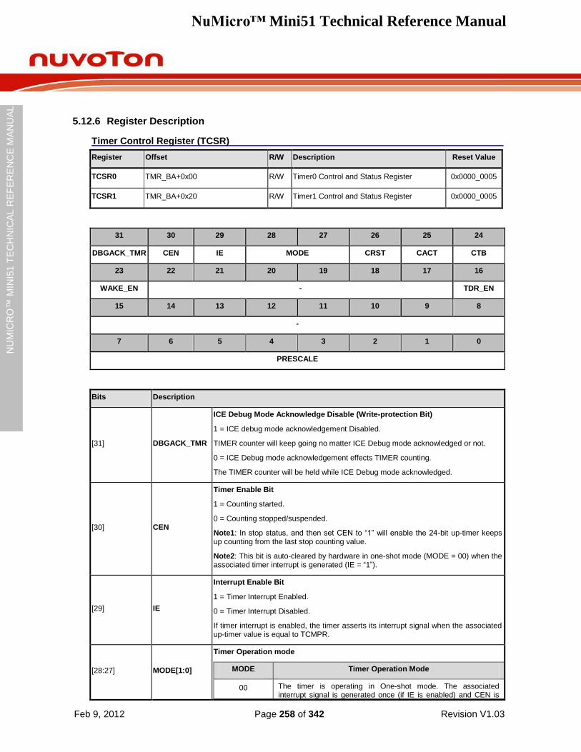
NuMicro™ Mini51 Technical Reference Manual
Feb 9, 2012 Page 258 of 342 Revision V1.03
NU
MIC
RO
™ M
INI5
1 T
EC
HN
ICA
L R
EF
ER
EN
CE
MA
NU
AL
5.12.6 Register Description
Timer Control Register (TCSR)
Register Offset R/W Description Reset Value
TCSR0 TMR_BA+0x00 R/W Timer0 Control and Status Register 0x0000_0005
TCSR1 TMR_BA+0x20 R/W Timer1 Control and Status Register 0x0000_0005
31 30 29 28 27 26 25 24
DBGACK_TMR CEN IE MODE CRST CACT CTB
23 22 21 20 19 18 17 16
WAKE_EN - TDR_EN
15 14 13 12 11 10 9 8
-
7 6 5 4 3 2 1 0
PRESCALE
Bits Description
[31] DBGACK_TMR
ICE Debug Mode Acknowledge Disable (Write-protection Bit)
1 = ICE debug mode acknowledgement Disabled.
TIMER counter will keep going no matter ICE Debug mode acknowledged or not.
0 = ICE Debug mode acknowledgement effects TIMER counting.
The TIMER counter will be held while ICE Debug mode acknowledged.
[30] CEN
Timer Enable Bit
1 = Counting started.
0 = Counting stopped/suspended.
Note1: In stop status, and then set CEN to “1” will enable the 24-bit up-timer keeps up counting from the last stop counting value.
Note2: This bit is auto-cleared by hardware in one-shot mode (MODE = 00) when the associated timer interrupt is generated (IE = “1”).
[29] IE
Interrupt Enable Bit
1 = Timer Interrupt Enabled.
0 = Timer Interrupt Disabled.
If timer interrupt is enabled, the timer asserts its interrupt signal when the associated up-timer value is equal to TCMPR.
[28:27] MODE[1:0]
Timer Operation mode
MODE Timer Operation Mode
00 The timer is operating in One-shot mode. The associated interrupt signal is generated once (if IE is enabled) and CEN is
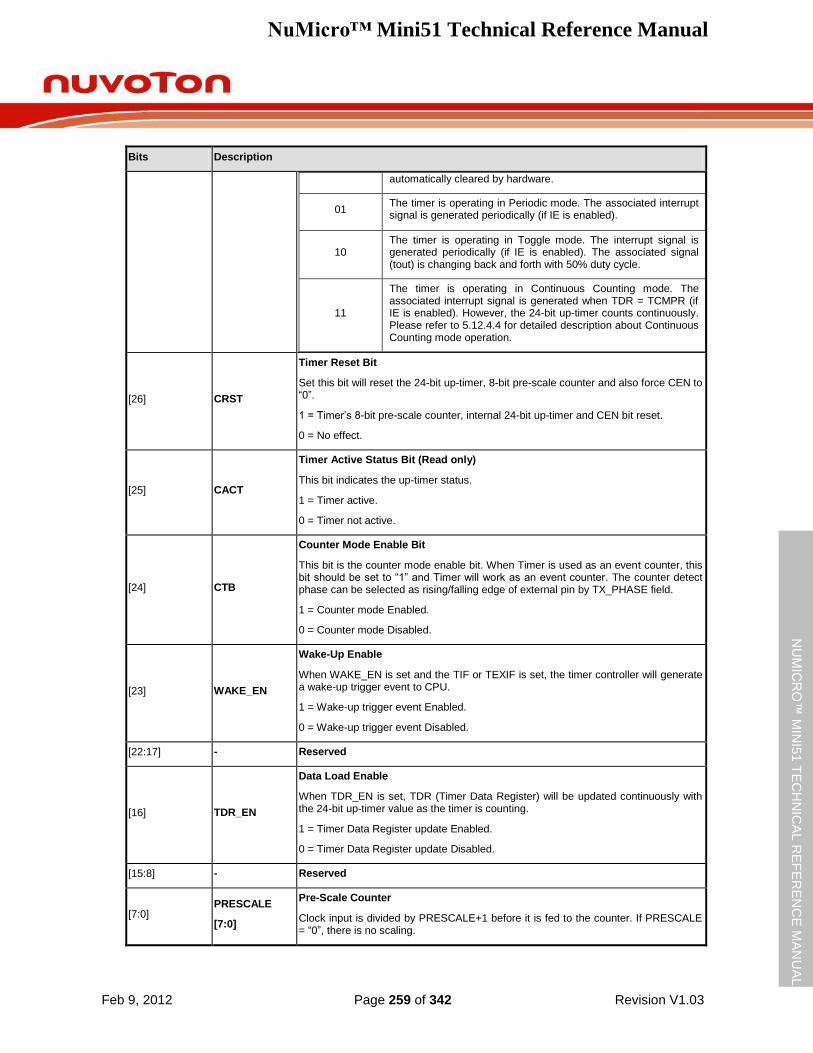
NuMicro™ Mini51 Technical Reference Manual
Feb 9, 2012 Page 259 of 342 Revision V1.03
NU
MIC
RO
™ M
INI5
1 T
EC
HN
ICA
L R
EF
ER
EN
CE
MA
NU
AL
Bits Description
automatically cleared by hardware.
01 The timer is operating in Periodic mode. The associated interrupt signal is generated periodically (if IE is enabled).
10 The timer is operating in Toggle mode. The interrupt signal is generated periodically (if IE is enabled). The associated signal (tout) is changing back and forth with 50% duty cycle.
11
The timer is operating in Continuous Counting mode. The associated interrupt signal is generated when TDR = TCMPR (if IE is enabled). However, the 24-bit up-timer counts continuously. Please refer to 5.12.4.4 for detailed description about Continuous Counting mode operation.
[26] CRST
Timer Reset Bit
Set this bit will reset the 24-bit up-timer, 8-bit pre-scale counter and also force CEN to “0”.
1 = Timer‟s 8-bit pre-scale counter, internal 24-bit up-timer and CEN bit reset.
0 = No effect.
[25] CACT
Timer Active Status Bit (Read only)
This bit indicates the up-timer status.
1 = Timer active.
0 = Timer not active.
[24] CTB
Counter Mode Enable Bit
This bit is the counter mode enable bit. When Timer is used as an event counter, this bit should be set to “1” and Timer will work as an event counter. The counter detect phase can be selected as rising/falling edge of external pin by TX_PHASE field.
1 = Counter mode Enabled.
0 = Counter mode Disabled.
[23] WAKE_EN
Wake-Up Enable
When WAKE_EN is set and the TIF or TEXIF is set, the timer controller will generate a wake-up trigger event to CPU.
1 = Wake-up trigger event Enabled.
0 = Wake-up trigger event Disabled.
[22:17] - Reserved
[16] TDR_EN
Data Load Enable
When TDR_EN is set, TDR (Timer Data Register) will be updated continuously with the 24-bit up-timer value as the timer is counting.
1 = Timer Data Register update Enabled.
0 = Timer Data Register update Disabled.
[15:8] - Reserved
[7:0] PRESCALE
[7:0]
Pre-Scale Counter
Clock input is divided by PRESCALE+1 before it is fed to the counter. If PRESCALE = “0”, there is no scaling.
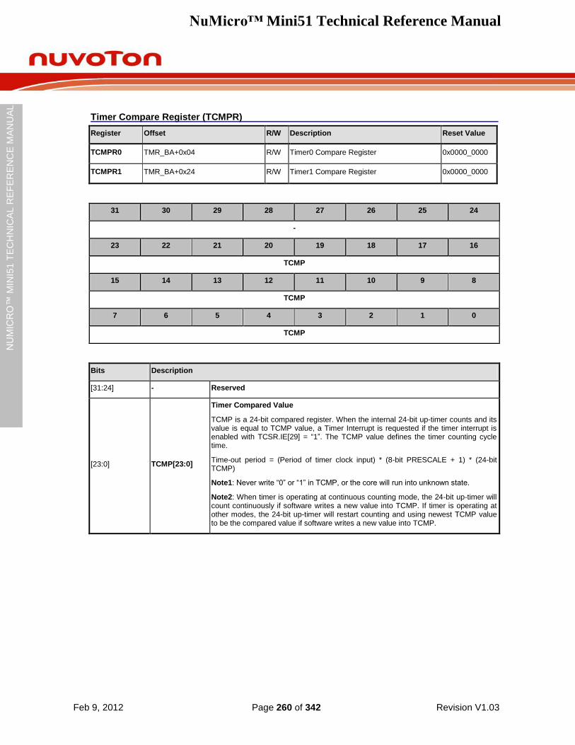
NuMicro™ Mini51 Technical Reference Manual
Feb 9, 2012 Page 260 of 342 Revision V1.03
NU
MIC
RO
™ M
INI5
1 T
EC
HN
ICA
L R
EF
ER
EN
CE
MA
NU
AL
Timer Compare Register (TCMPR)
Register Offset R/W Description Reset Value
TCMPR0 TMR_BA+0x04 R/W Timer0 Compare Register 0x0000_0000
TCMPR1 TMR_BA+0x24 R/W Timer1 Compare Register 0x0000_0000
31 30 29 28 27 26 25 24
-
23 22 21 20 19 18 17 16
TCMP
15 14 13 12 11 10 9 8
TCMP
7 6 5 4 3 2 1 0
TCMP
Bits Description
[31:24] - Reserved
[23:0] TCMP[23:0]
Timer Compared Value
TCMP is a 24-bit compared register. When the internal 24-bit up-timer counts and its value is equal to TCMP value, a Timer Interrupt is requested if the timer interrupt is enabled with TCSR.IE[29] = “1”. The TCMP value defines the timer counting cycle time.
Time-out period = (Period of timer clock input) * (8-bit PRESCALE + 1) * (24-bit TCMP)
Note1: Never write “0” or “1” in TCMP, or the core will run into unknown state.
Note2: When timer is operating at continuous counting mode, the 24-bit up-timer will count continuously if software writes a new value into TCMP. If timer is operating at other modes, the 24-bit up-timer will restart counting and using newest TCMP value to be the compared value if software writes a new value into TCMP.
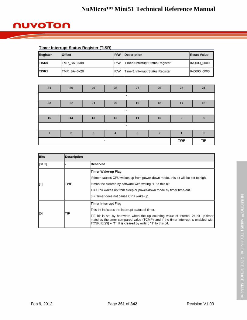
NuMicro™ Mini51 Technical Reference Manual
Feb 9, 2012 Page 261 of 342 Revision V1.03
NU
MIC
RO
™ M
INI5
1 T
EC
HN
ICA
L R
EF
ER
EN
CE
MA
NU
AL
Timer Interrupt Status Register (TISR)
Register Offset R/W Description Reset Value
TISR0 TMR_BA+0x08 R/W Timer0 Interrupt Status Register 0x0000_0000
TISR1 TMR_BA+0x28 R/W Timer1 Interrupt Status Register 0x0000_0000
31 30 29 28 27 26 25 24
-
23 22 21 20 19 18 17 16
-
15 14 13 12 11 10 9 8
-
7 6 5 4 3 2 1 0
- TWF TIF
Bits Description
[31:2] - Reserved
[1] TWF
Timer Wake-up Flag
If timer causes CPU wakes up from power-down mode, this bit will be set to high.
It must be cleared by software with writing “1” to this bit.
1 = CPU wakes up from sleep or power-down mode by timer time-out.
0 = Timer does not cause CPU wake-up.
[0] TIF
Timer Interrupt Flag
This bit indicates the interrupt status of timer.
TIF bit is set by hardware when the up counting value of internal 24-bit up-timer matches the timer compared value (TCMP) and if the timer interrupt is enabled with TCSR.IE[29] = “1”. It is cleared by writing “1” to this bit.
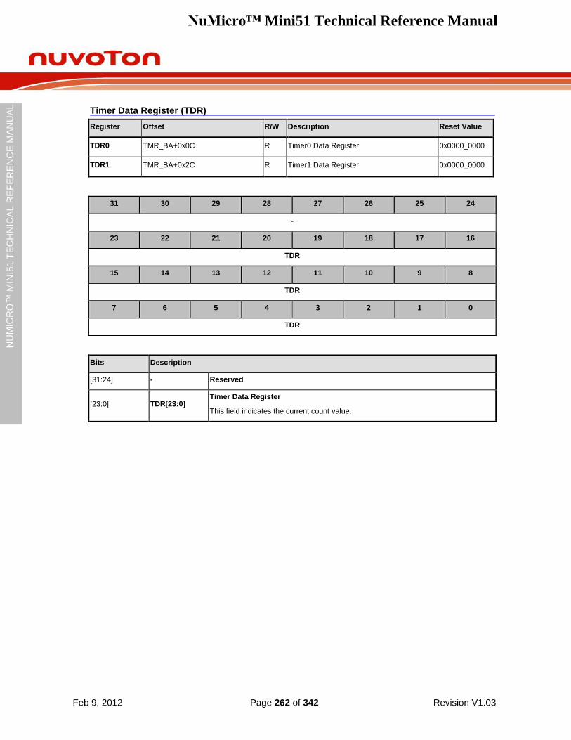
NuMicro™ Mini51 Technical Reference Manual
Feb 9, 2012 Page 262 of 342 Revision V1.03
NU
MIC
RO
™ M
INI5
1 T
EC
HN
ICA
L R
EF
ER
EN
CE
MA
NU
AL
Timer Data Register (TDR)
Register Offset R/W Description Reset Value
TDR0 TMR_BA+0x0C R Timer0 Data Register 0x0000_0000
TDR1 TMR_BA+0x2C R Timer1 Data Register 0x0000_0000
31 30 29 28 27 26 25 24
-
23 22 21 20 19 18 17 16
TDR
15 14 13 12 11 10 9 8
TDR
7 6 5 4 3 2 1 0
TDR
Bits Description
[31:24] - Reserved
[23:0] TDR[23:0] Timer Data Register
This field indicates the current count value.
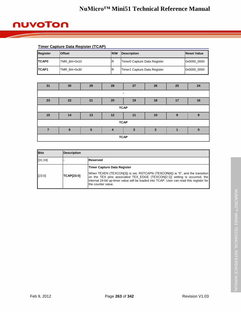
NuMicro™ Mini51 Technical Reference Manual
Feb 9, 2012 Page 263 of 342 Revision V1.03
NU
MIC
RO
™ M
INI5
1 T
EC
HN
ICA
L R
EF
ER
EN
CE
MA
NU
AL
Timer Capture Data Register (TCAP)
Register Offset R/W Description Reset Value
TCAP0 TMR_BA+0x10 R Timer0 Capture Data Register 0x0000_0000
TCAP1 TMR_BA+0x30 R Timer1 Capture Data Register 0x0000_0000
31 30 29 28 27 26 25 24
-
23 22 21 20 19 18 17 16
TCAP
15 14 13 12 11 10 9 8
TCAP
7 6 5 4 3 2 1 0
TCAP
Bits Description
[31:24] - Reserved
[23:0] TCAP[23:0]
Timer Capture Data Register
When TEXEN (TEXCON[3]) is set, RSTCAPN (TEXCON[4]) is “0”, and the transition on the TEX pins associated TEX_EDGE (TEXCON[2:1]) setting is occurred, the internal 24-bit up-timer value will be loaded into TCAP. User can read this register for the counter value.
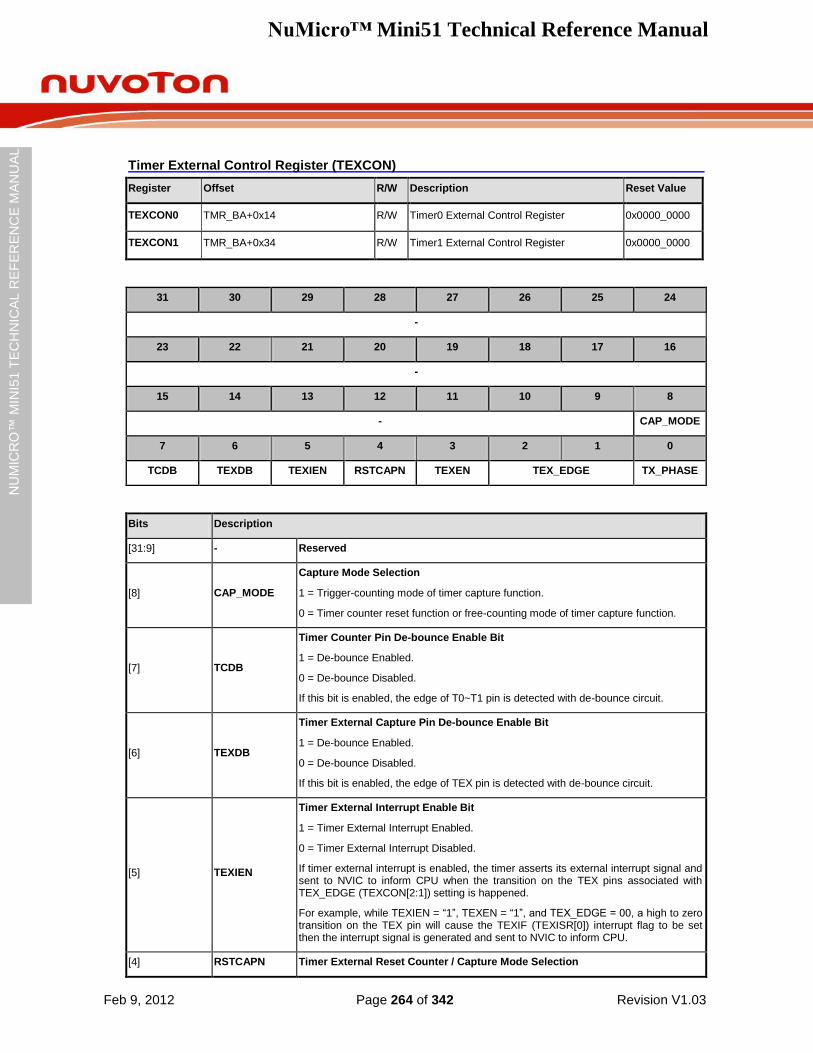
NuMicro™ Mini51 Technical Reference Manual
Feb 9, 2012 Page 264 of 342 Revision V1.03
NU
MIC
RO
™ M
INI5
1 T
EC
HN
ICA
L R
EF
ER
EN
CE
MA
NU
AL
Timer External Control Register (TEXCON)
Register Offset R/W Description Reset Value
TEXCON0 TMR_BA+0x14 R/W Timer0 External Control Register 0x0000_0000
TEXCON1 TMR_BA+0x34 R/W Timer1 External Control Register 0x0000_0000
31 30 29 28 27 26 25 24
-
23 22 21 20 19 18 17 16
-
15 14 13 12 11 10 9 8
- CAP_MODE
7 6 5 4 3 2 1 0
TCDB TEXDB TEXIEN RSTCAPN TEXEN TEX_EDGE TX_PHASE
Bits Description
[31:9] - Reserved
[8] CAP_MODE
Capture Mode Selection
1 = Trigger-counting mode of timer capture function.
0 = Timer counter reset function or free-counting mode of timer capture function.
[7] TCDB
Timer Counter Pin De-bounce Enable Bit
1 = De-bounce Enabled.
0 = De-bounce Disabled.
If this bit is enabled, the edge of T0~T1 pin is detected with de-bounce circuit.
[6] TEXDB
Timer External Capture Pin De-bounce Enable Bit
1 = De-bounce Enabled.
0 = De-bounce Disabled.
If this bit is enabled, the edge of TEX pin is detected with de-bounce circuit.
[5] TEXIEN
Timer External Interrupt Enable Bit
1 = Timer External Interrupt Enabled.
0 = Timer External Interrupt Disabled.
If timer external interrupt is enabled, the timer asserts its external interrupt signal and sent to NVIC to inform CPU when the transition on the TEX pins associated with TEX_EDGE (TEXCON[2:1]) setting is happened.
For example, while TEXIEN = “1”, TEXEN = “1”, and TEX_EDGE = 00, a high to zero transition on the TEX pin will cause the TEXIF (TEXISR[0]) interrupt flag to be set then the interrupt signal is generated and sent to NVIC to inform CPU.
[4] RSTCAPN Timer External Reset Counter / Capture Mode Selection
NuMicro™ Mini51 Technical Reference Manual
Feb 9, 2012 Page 265 of 342 Revision V1.03
NU
MIC
RO
™ M
INI5
1 T
EC
HN
ICA
L R
EF
ER
EN
CE
MA
NU
AL
Bits Description
1 = TEX transition is used as the timer counter reset function.
0 = TEX transition is used as the timer capture function.
[3] TEXEN
Timer External Pin Enable
This bit enables the reset/capture function on the TEX pin.
1 = The transition detected on the TEX pin will result in capture or reset of timer counter.
0 = The TEX pin will be ignored.
[2:1] TEX_EDGE
[1:0]
Timer External Pin Edge Detection
TEX_EDGE Description
00 A high to zero transition on TEX will be detected.
01 A zero to high transition on TEX will be detected.
10 Either high to zero or zero to high transition on TEX will be detected.
11 Reserved.
[0] TX_PHASE
Timer External Count Phase
This bit indicates the external count pin phase.
1 = A rising edge of external count pin will be counted.
0 = A falling edge of external count pin will be counted.
NuMicro™ Mini51 Technical Reference Manual
Feb 9, 2012 Page 266 of 342 Revision V1.03
NU
MIC
RO
™ M
INI5
1 T
EC
HN
ICA
L R
EF
ER
EN
CE
MA
NU
AL
Timer External Interrupt Status Register (TEXISR)
Register Offset R/W Description Reset Value
TEXISR0 TMR_BA+0x18 R/W Timer0 External Interrupt Status Register 0x0000_0000
TEXISR1 TMR_BA+0x38 R/W Timer1 External Interrupt Status Register 0x0000_0000
31 30 29 28 27 26 25 24
-
23 22 21 20 19 18 17 16
-
15 14 13 12 11 10 9 8
-
7 6 5 4 3 2 1 0
- TEXIF
Bits Description
[31:1] - Reserved
[0] TEXIF
Timer External Interrupt Flag
This bit indicates the external interrupt status of the timer.
This bit is set by hardware when TEXEN (TEXCON[3]) is set “1”, and the transition on the TEX pins associated with TEX_EDGE (TEXCON[2:1]) setting occurred. It is cleared by writing “1” to this bit.
For example, while TEXEN = “1”, and TEX_EDGE = 00, a high to zero transition on the TEX pin causes the TEXIF to be set.

NuMicro™ Mini51 Technical Reference Manual
Feb 9, 2012 Page 267 of 342 Revision V1.03
NU
MIC
RO
™ M
INI5
1 T
EC
HN
ICA
L R
EF
ER
EN
CE
MA
NU
AL
5.13 UART Interface Controller
The NuMicro Mini51 series provides one channel of Universal Asynchronous Receiver/Transmitters (UART). UART performs Normal Speed UART, and support flow control function.
5.13.1 Overview
The Universal Asynchronous Receiver/Transmitter (UART) performs a serial-to-parallel conversion on data received from the peripheral, and a parallel-to-serial conversion on data transmitted from the CPU. The UART controller also supports IrDA SIR function, and RS-485 mode functions. Each UART channel supports six types of interrupts, including transmitter FIFO empty interrupt (INT_THRE), receiver threshold level reaching interrupt (INT_RDA), line status interrupt (parity error or framing error or break interrupt) (INT_RLS), receiver buffer time-out interrupt (INT_TOUT), MODEM/Wake-up status interrupt (INT_MODEM), and Buffer error interrupt (INT_BUF_ERR). Interrupt number 12 (vector number is 28) supports UART interrupt. Refer to Nested Vectored Interrupt Controller chapter for System Interrupt Map.
The UART is built-in with a 16-byte transmitter FIFO (TX_FIFO) and a 16-byte receiver FIFO (RX_FIFO) that reduces the number of interrupts presented to the CPU and the CPU can read the status of the UART at any time during the operation. The reported status information includes the type and condition of the transfer operations being performed by the UART, as well as 4 error conditions (parity error, framing error, break interrupt and buffer error) probably occur while receiving data. The UART includes a programmable baud rate generator that is capable of dividing crystal clock input by divisors to produce the clock that transmitter and receiver need. The baud rate equation is Baud Rate = UART_CLK / M * [BRD + 2], where M and BRD are defined in Baud Rate Divider Register (UA_BAUD). The following table lists the equations in the various conditions and the UART baud rate setting table.
Table 5.13-1 UART Baud Rate Setting Table
Mode DIV_X_EN DIV_X_ONE Divider X BRD Baud Rate Equation
0 0 0 B A UART_CLK / [16 * (A+2)]
1 1 0 B A UART_CLK / [(B+1) * (A+2)] , B must >= 8
2 1 1 Don‟t care A UART_CLK / (A+2), A must >=3
Table 5.13-2 UART Baud Rate Setting Table
System clock = 22.1184 MHz
Baud rate Mode0 Mode1 Mode2
921600 Not Support A=0, B=11 A=22
460800 A=1 A=1, B=15 A=2, B=11
A=46
230400 A=4 A=4, B=15 A=6, B=11
A=94
115200 A=10 A=10, B=15 A=190

NuMicro™ Mini51 Technical Reference Manual
Feb 9, 2012 Page 268 of 342 Revision V1.03
NU
MIC
RO
™ M
INI5
1 T
EC
HN
ICA
L R
EF
ER
EN
CE
MA
NU
AL
A=14, B=11
57600 A=22 A=22, B=15 A=30, B=11
A=382
38400 A=34 A=62, B=8 A=46, B=11 A=34, B=15
A=574
19200 A=70 A=126, B=8 A=94, B=11 A=70, B=15
A=1150
9600 A=142 A=254, B=8 A=190, B=11 A=142, B=15
A=2302
4800 A=286 A=510, B=8 A=382, B=11 A=286, B=15
A=4606
5.13.1.1 Auto-Flow Control
The UART controller supports auto-flow control function that uses two low-level signals, CTSn (clear-to-send) and RTSn (request-to-send), to control the flow of data transfer between the UART and external devices (ex: Modem). When auto-flow is enabled, the UART is not allowed to receive data until the UART asserts RTSn to external device. When the number of bytes in the RX FIFO equals the value of RTS_TRI_LEV (UA_FCR[19:16]), the RTSn is de-asserted. The UART sends data out when UART controller detects CTSn is asserted from external device. If a validly asserted CTSn is not detected the UART controller will not send data out.
5.13.1.2 IrDA Function Mode
The UART controllers also provides Serial IrDA (SIR, Serial Infrared) function (user must set IrDA_EN (UA_FUN_SEL[1:0]) to enable IrDA function). The SIR specification defines a short-range infrared asynchronous serial transmission mode with one start bit, 8 data bits, and 1 stop bit. The maximum data rate is 115.2 Kbps (half duplex). The IrDA SIR block contains an IrDA SIR Protocol encoder/decoder. The IrDA SIR protocol is half-duplex only. Thus it cannot transmit and receive data at the same time. The IrDA SIR physical layer specifies a minimum 10ms transfer delay between transmission and reception. This delay feature must be implemented by software.
5.13.1.3 RS-485 Function Mode
Alternate function of UART controllers is RS-485 9 bit mode function, direction control provided by RTSn pin or can program GPIO (P0.1 for RTSn) to implement the function by software. The RS-485 mode is selected by setting the UA_FUN_SEL register to select RS-485 function. The RS-485 driver control is implemented using the RTSn control signal from an asynchronous serial port to enable the RS-485 driver. In RS-485 mode, many characteristics of the RX and TX are the same as UART.
NuMicro™ Mini51 Technical Reference Manual
Feb 9, 2012 Page 269 of 342 Revision V1.03
NU
MIC
RO
™ M
INI5
1 T
EC
HN
ICA
L R
EF
ER
EN
CE
MA
NU
AL
5.13.2 Features
Full duplex, asynchronous communications
Separates receive/transmit 16 bytes entry FIFO for data payloads
Supports hardware auto flow control/flow control function (CTSn, RTSn) and programmable RTSn flow control trigger level
Programmable receiver buffer trigger level
Supports programmable baud-rate generator for each channel individually
Supports CTSn wake-up function
Supports 7-bit receiver buffer time-out detection function
Programmable transmitting data delay time between the last stop and the next start bit by setting UA_TOR[DLY] register
Supports break error, frame error, parity error and receive/transmit buffer overflow detection function
Fully programmable serial-interface characteristics
Programmable number of data bit, 5, 6, 7, 8 character
Programmable parity bit, even, odd, no parity or stick parity bit generation and detection
Programmable stop bit, 1, 1.5, or 2 stop bit generation
Supports IrDA SIR function mode
Supports 3/16-bit duration for normal mode
Supports RS-485 function mode
Supports RS-485 9-bit mode
Supports hardware or software RTSn control or software GPIO control to control transfer direction
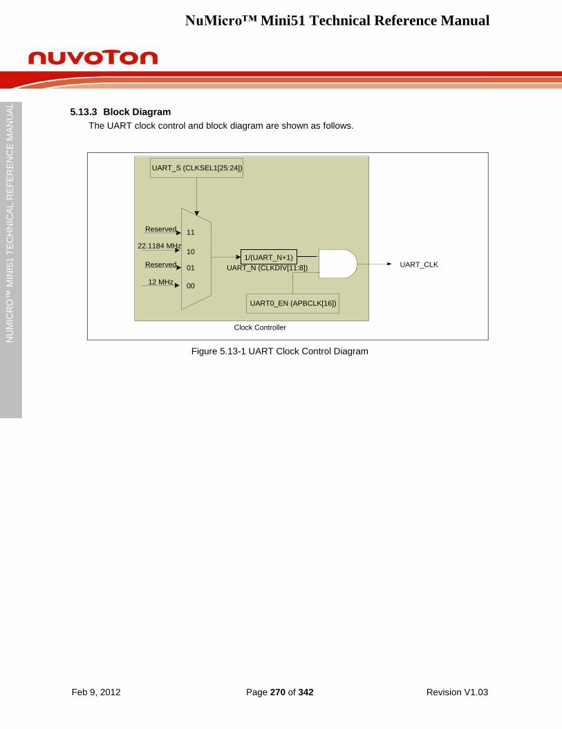
NuMicro™ Mini51 Technical Reference Manual
Feb 9, 2012 Page 270 of 342 Revision V1.03
NU
MIC
RO
™ M
INI5
1 T
EC
HN
ICA
L R
EF
ER
EN
CE
MA
NU
AL
5.13.3 Block Diagram
The UART clock control and block diagram are shown as follows.
UART0_EN (APBCLK[16])
Clock Controller
UART_CLK
UART_S (CLKSEL1[25:24])
00
01
10
11
12 MHz
Reserved
22.1184 MHz
Reserved
UART_N (CLKDIV[11:8])
1/(UART_N+1)
Figure 5.13-1 UART Clock Control Diagram
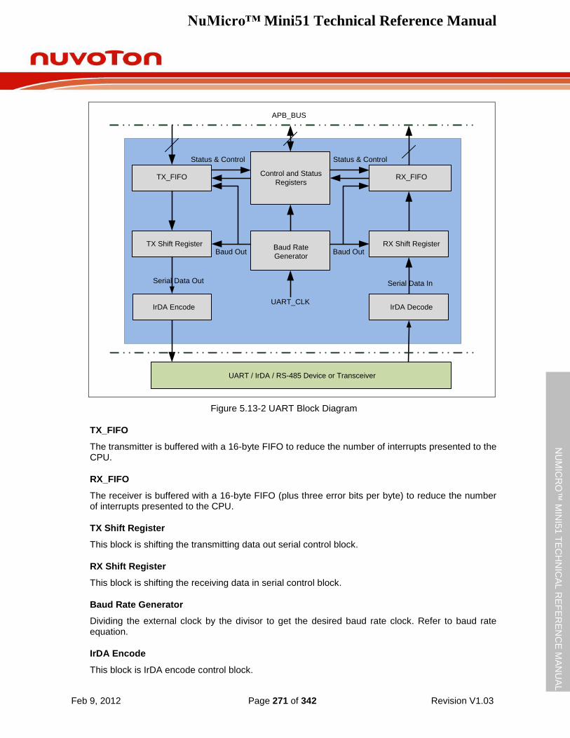
NuMicro™ Mini51 Technical Reference Manual
Feb 9, 2012 Page 271 of 342 Revision V1.03
NU
MIC
RO
™ M
INI5
1 T
EC
HN
ICA
L R
EF
ER
EN
CE
MA
NU
AL
APB_BUS
UART / IrDA / RS-485 Device or Transceiver
UART_CLKIrDA Decode
RX Shift Register
RX_FIFOTX_FIFO
TX Shift Register
IrDA Encode
Baud Rate
Generator
Control and Status
Registers
Serial Data InSerial Data Out
Baud OutBaud Out
Status & Control Status & Control
Figure 5.13-2 UART Block Diagram
TX_FIFO
The transmitter is buffered with a 16-byte FIFO to reduce the number of interrupts presented to the CPU.
RX_FIFO
The receiver is buffered with a 16-byte FIFO (plus three error bits per byte) to reduce the number of interrupts presented to the CPU.
TX Shift Register
This block is shifting the transmitting data out serial control block.
RX Shift Register
This block is shifting the receiving data in serial control block.
Baud Rate Generator
Dividing the external clock by the divisor to get the desired baud rate clock. Refer to baud rate equation.
IrDA Encode
This block is IrDA encode control block.
NuMicro™ Mini51 Technical Reference Manual
Feb 9, 2012 Page 272 of 342 Revision V1.03
NU
MIC
RO
™ M
INI5
1 T
EC
HN
ICA
L R
EF
ER
EN
CE
MA
NU
AL
IrDA Decode
This block is IrDA decode control block.
Control and Status Register
This field is a register set which includes the FIFO control registers (UA_FCR), FIFO status registers (UA_FSR), and line control register (UA_LCR) for transmitter and receiver. The time-out control register (UA_TOR) identifies the condition of time-out interrupt. This register set also includes the interrupt enable register (UA_IER) and interrupt status register (UA_ISR) to enable or disable the responding interrupt and to identify the occurrence of the responding interrupt. There are six types of interrupts, including transmitter FIFO empty interrupt (INT_THRE), receiver threshold level reaching interrupt (INT_RDA), line status interrupt (parity error or framing error or break interrupt) (INT_RLS) , time-out interrupt (INT_TOUT), MODEM/Wake-up status interrupt (INT_MODEM), and Buffer error interrupt (INT_BUF_ERR).
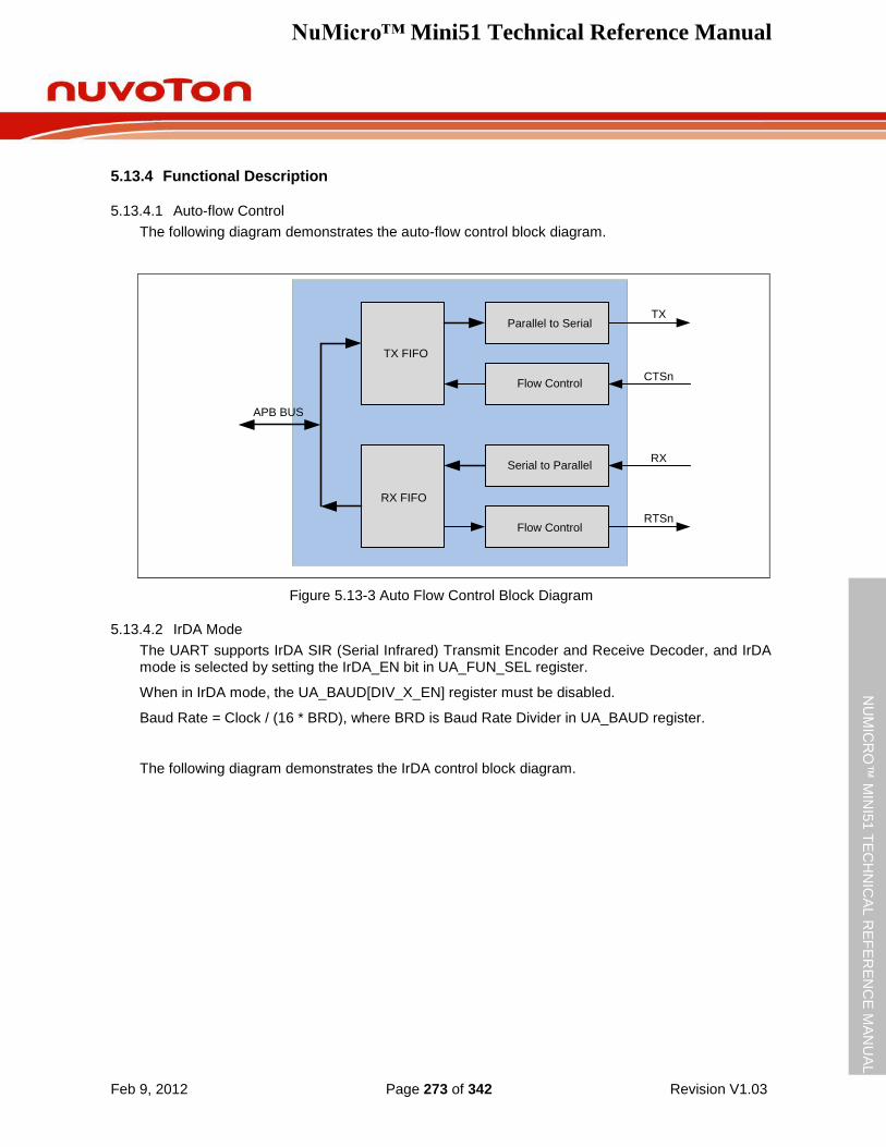
NuMicro™ Mini51 Technical Reference Manual
Feb 9, 2012 Page 273 of 342 Revision V1.03
NU
MIC
RO
™ M
INI5
1 T
EC
HN
ICA
L R
EF
ER
EN
CE
MA
NU
AL
5.13.4 Functional Description
5.13.4.1 Auto-flow Control
The following diagram demonstrates the auto-flow control block diagram.
APB BUS
TX
CTSn
RX
RTSn
Parallel to Serial
Flow Control
Serial to Parallel
Flow Control
TX FIFO
RX FIFO
Figure 5.13-3 Auto Flow Control Block Diagram
5.13.4.2 IrDA Mode
The UART supports IrDA SIR (Serial Infrared) Transmit Encoder and Receive Decoder, and IrDA mode is selected by setting the IrDA_EN bit in UA_FUN_SEL register.
When in IrDA mode, the UA_BAUD[DIV_X_EN] register must be disabled.
Baud Rate = Clock / (16 * BRD), where BRD is Baud Rate Divider in UA_BAUD register.
The following diagram demonstrates the IrDA control block diagram.
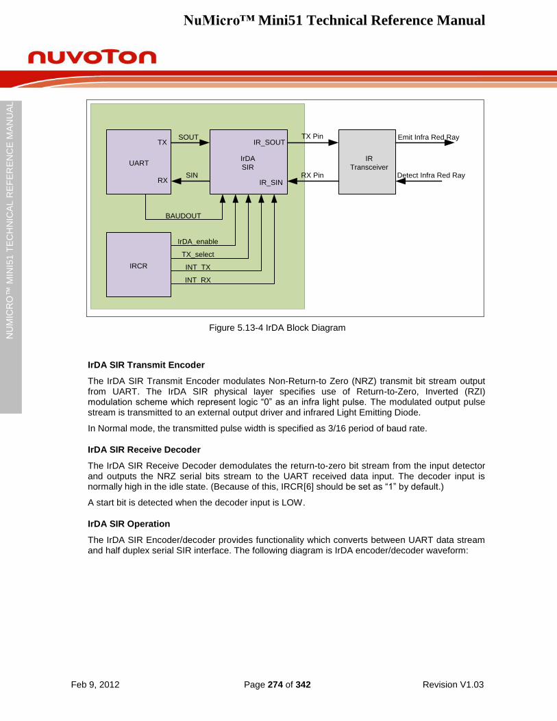
NuMicro™ Mini51 Technical Reference Manual
Feb 9, 2012 Page 274 of 342 Revision V1.03
NU
MIC
RO
™ M
INI5
1 T
EC
HN
ICA
L R
EF
ER
EN
CE
MA
NU
AL
Emit Infra Red Ray
Detect Infra Red Ray
IR
Transceiver
IrDA
SIR
IRCR
UART
TX Pin
RX Pin
IrDA_enable
TX_select
INT_TX
INT_RX
BAUDOUT
IR_SOUT
IR_SIN
SOUT
SIN
TX
RX
Figure 5.13-4 IrDA Block Diagram
IrDA SIR Transmit Encoder
The IrDA SIR Transmit Encoder modulates Non-Return-to Zero (NRZ) transmit bit stream output from UART. The IrDA SIR physical layer specifies use of Return-to-Zero, Inverted (RZI) modulation scheme which represent logic “0” as an infra light pulse. The modulated output pulse stream is transmitted to an external output driver and infrared Light Emitting Diode.
In Normal mode, the transmitted pulse width is specified as 3/16 period of baud rate.
IrDA SIR Receive Decoder
The IrDA SIR Receive Decoder demodulates the return-to-zero bit stream from the input detector and outputs the NRZ serial bits stream to the UART received data input. The decoder input is normally high in the idle state. (Because of this, IRCR[6] should be set as “1” by default.)
A start bit is detected when the decoder input is LOW.
IrDA SIR Operation
The IrDA SIR Encoder/decoder provides functionality which converts between UART data stream and half duplex serial SIR interface. The following diagram is IrDA encoder/decoder waveform:
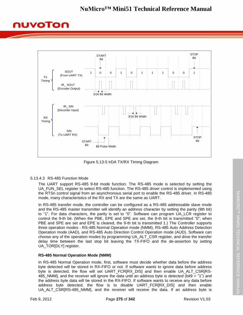
NuMicro™ Mini51 Technical Reference Manual
Feb 9, 2012 Page 275 of 342 Revision V1.03
NU
MIC
RO
™ M
INI5
1 T
EC
HN
ICA
L R
EF
ER
EN
CE
MA
NU
AL
SOUT
(From UART TX)
IR_ SOUT
(Encoder Output)
IR_ SIN
(Decorder Input)
SIN
(To UART RX)
01
Bit Pulse Width
STOP
BitSTART
Bit
START
Bit
TX
Timing
RX
Timing
3/16 Bit Width
0 1 0 1 1 1 0 0 1
3/16 Bit Width
STOP
Bit
Figure 5.13-5 IrDA TX/RX Timing Diagram
5.13.4.3 RS-485 Function Mode
The UART support RS-485 9-bit mode function. The RS-485 mode is selected by setting the UA_FUN_SEL register to select RS-485 function. The RS-485 driver control is implemented using the RTSn control signal from an asynchronous serial port to enable the RS-485 driver. In RS-485 mode, many characteristics of the RX and TX are the same as UART.
In RS-485 transfer mode, the controller can be configured as a RS-485 addressable slave mode and the RS-485 master transmitter will identify an address character by setting the parity (9th bit) to “1”. For data characters, the parity is set to “0”. Software can program UA_LCR register to control the 9-th bit. (When the PBE, EPE and SPE are set, the 9-th bit is transmitted “0”; when PBE and SPE are set and EPE is cleared, the 9-th bit is transmitted 1.) The Controller supports three operation modes - RS-485 Normal Operation mode (NMM), RS-485 Auto Address Detection Operation mode (AAD), and RS-485 Auto Direction Control Operation mode (AUD). Software can choose any of the operation modes by programming UA_ALT_CSR register, and drive the transfer delay time between the last stop bit leaving the TX-FIFO and the de-assertion by setting UA_TOR[DLY] register.
RS-485 Normal Operation Mode (NMM)
In RS-485 Normal Operation mode, first, software must decide whether data before the address byte detected will be stored in RX-FIFO or not. If software wants to ignore data before address byte is detected, the flow will set UART_FCR[RX_DIS] and then enable UA_ALT_CSR[RS-485_NMM], and the receiver will ignore the data until an address byte is detected (bit9 = ”1”) and the address byte data will be stored in the RX-FIFO. If software wants to receive any data before address byte detected, the flow is to disable UART_FCR[RX_DIS] and then enable UA_ALT_CSR[RS-485_NMM], and the receiver will receive the data. If an address byte is
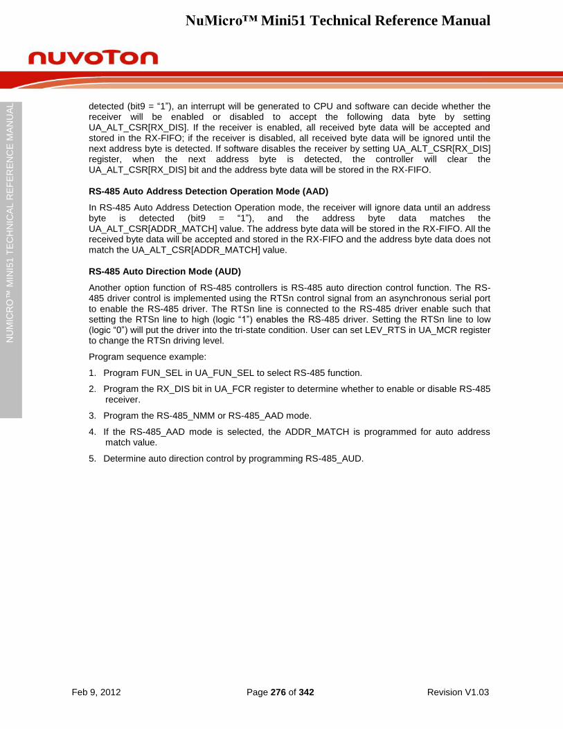
NuMicro™ Mini51 Technical Reference Manual
Feb 9, 2012 Page 276 of 342 Revision V1.03
NU
MIC
RO
™ M
INI5
1 T
EC
HN
ICA
L R
EF
ER
EN
CE
MA
NU
AL
detected (bit9 = “1”), an interrupt will be generated to CPU and software can decide whether the receiver will be enabled or disabled to accept the following data byte by setting UA_ALT_CSR[RX_DIS]. If the receiver is enabled, all received byte data will be accepted and stored in the RX-FIFO; if the receiver is disabled, all received byte data will be ignored until the next address byte is detected. If software disables the receiver by setting UA_ALT_CSR[RX_DIS] register, when the next address byte is detected, the controller will clear the UA_ALT_CSR[RX_DIS] bit and the address byte data will be stored in the RX-FIFO.
RS-485 Auto Address Detection Operation Mode (AAD)
In RS-485 Auto Address Detection Operation mode, the receiver will ignore data until an address byte is detected (bit9 = “1”), and the address byte data matches the UA_ALT_CSR[ADDR_MATCH] value. The address byte data will be stored in the RX-FIFO. All the received byte data will be accepted and stored in the RX-FIFO and the address byte data does not match the UA_ALT_CSR[ADDR_MATCH] value.
RS-485 Auto Direction Mode (AUD)
Another option function of RS-485 controllers is RS-485 auto direction control function. The RS-485 driver control is implemented using the RTSn control signal from an asynchronous serial port to enable the RS-485 driver. The RTSn line is connected to the RS-485 driver enable such that setting the RTSn line to high (logic “1”) enables the RS-485 driver. Setting the RTSn line to low (logic “0”) will put the driver into the tri-state condition. User can set LEV_RTS in UA_MCR register to change the RTSn driving level.
Program sequence example:
1. Program FUN_SEL in UA_FUN_SEL to select RS-485 function.
2. Program the RX_DIS bit in UA_FCR register to determine whether to enable or disable RS-485 receiver.
3. Program the RS-485_NMM or RS-485_AAD mode.
4. If the RS-485_AAD mode is selected, the ADDR_MATCH is programmed for auto address match value.
5. Determine auto direction control by programming RS-485_AUD.
NuMicro™ Mini51 Technical Reference Manual
Feb 9, 2012 Page 277 of 342 Revision V1.03
NU
MIC
RO
™ M
INI5
1 T
EC
HN
ICA
L R
EF
ER
EN
CE
MA
NU
AL
RX
TX
RTS
Drive Enable
UART/RS-485
Controller
RS-485 Transceiver
Differenitial Bus
STOP
TX
RTS Drive Enable
S D0 D1 D2 D3 D4 D5 D6 D7 P
Figure 5.13-6 Structure of RS-485 Frame
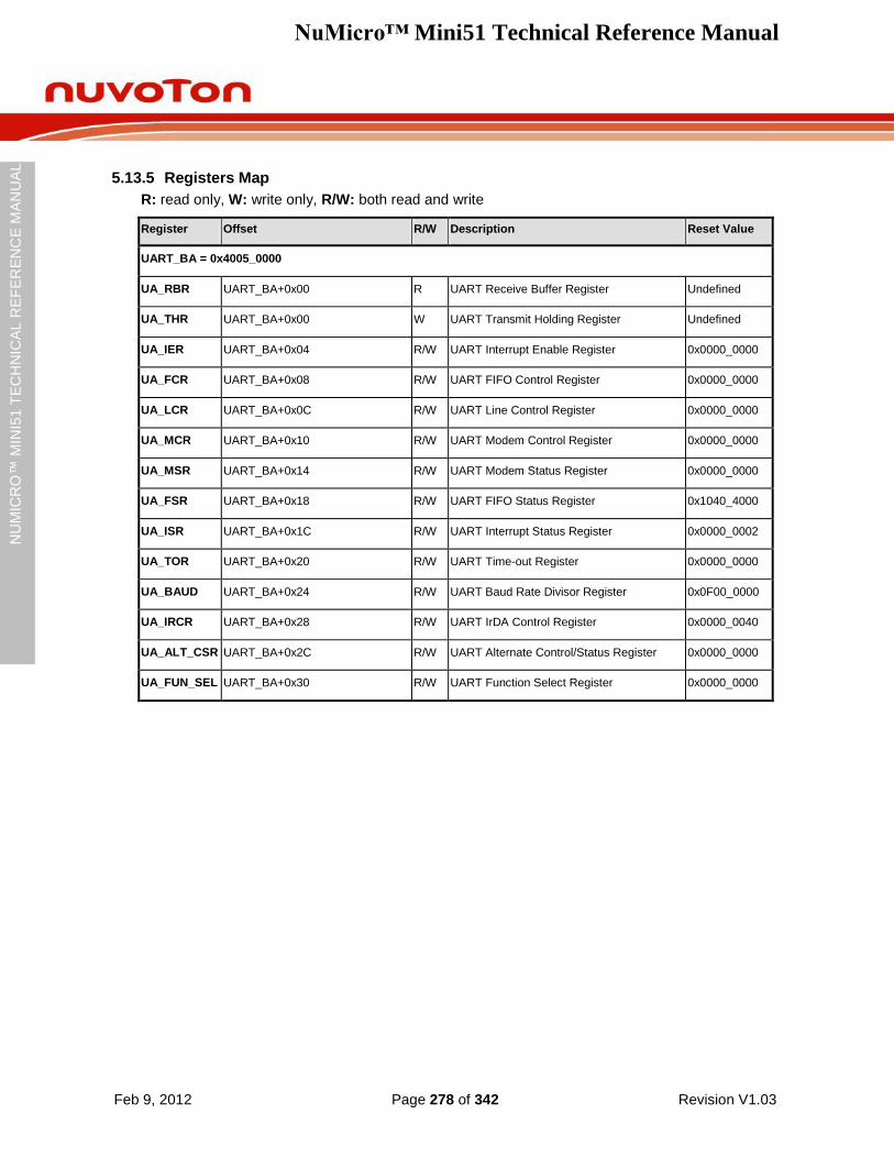
NuMicro™ Mini51 Technical Reference Manual
Feb 9, 2012 Page 278 of 342 Revision V1.03
NU
MIC
RO
™ M
INI5
1 T
EC
HN
ICA
L R
EF
ER
EN
CE
MA
NU
AL
5.13.5 Registers Map
R: read only, W: write only, R/W: both read and write
Register Offset R/W Description Reset Value
UART_BA = 0x4005_0000
UA_RBR UART_BA+0x00 R UART Receive Buffer Register Undefined
UA_THR UART_BA+0x00 W UART Transmit Holding Register Undefined
UA_IER UART_BA+0x04 R/W UART Interrupt Enable Register 0x0000_0000
UA_FCR UART_BA+0x08 R/W UART FIFO Control Register 0x0000_0000
UA_LCR UART_BA+0x0C R/W UART Line Control Register 0x0000_0000
UA_MCR UART_BA+0x10 R/W UART Modem Control Register 0x0000_0000
UA_MSR UART_BA+0x14 R/W UART Modem Status Register 0x0000_0000
UA_FSR UART_BA+0x18 R/W UART FIFO Status Register 0x1040_4000
UA_ISR UART_BA+0x1C R/W UART Interrupt Status Register 0x0000_0002
UA_TOR UART_BA+0x20 R/W UART Time-out Register 0x0000_0000
UA_BAUD UART_BA+0x24 R/W UART Baud Rate Divisor Register 0x0F00_0000
UA_IRCR UART_BA+0x28 R/W UART IrDA Control Register 0x0000_0040
UA_ALT_CSR UART_BA+0x2C R/W UART Alternate Control/Status Register 0x0000_0000
UA_FUN_SEL UART_BA+0x30 R/W UART Function Select Register 0x0000_0000
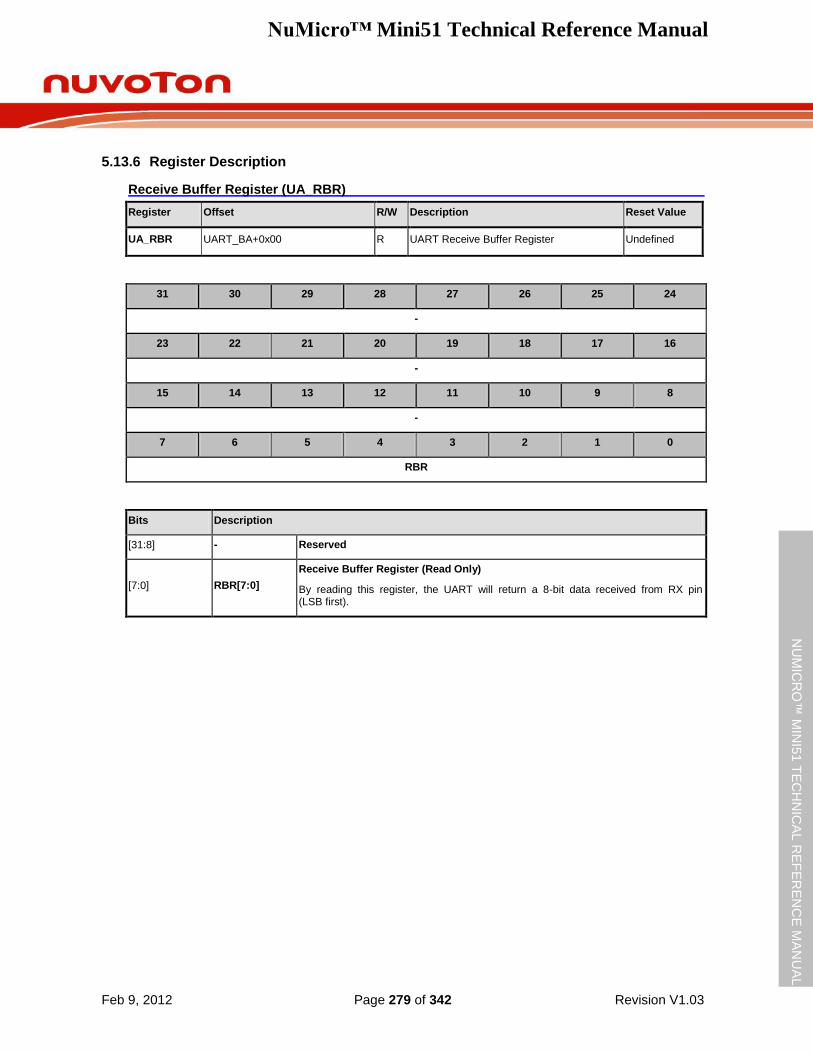
NuMicro™ Mini51 Technical Reference Manual
Feb 9, 2012 Page 279 of 342 Revision V1.03
NU
MIC
RO
™ M
INI5
1 T
EC
HN
ICA
L R
EF
ER
EN
CE
MA
NU
AL
5.13.6 Register Description
Receive Buffer Register (UA_RBR)
Register Offset R/W Description Reset Value
UA_RBR UART_BA+0x00 R UART Receive Buffer Register Undefined
31 30 29 28 27 26 25 24
-
23 22 21 20 19 18 17 16
-
15 14 13 12 11 10 9 8
-
7 6 5 4 3 2 1 0
RBR
Bits Description
[31:8] - Reserved
[7:0] RBR[7:0]
Receive Buffer Register (Read Only)
By reading this register, the UART will return a 8-bit data received from RX pin (LSB first).
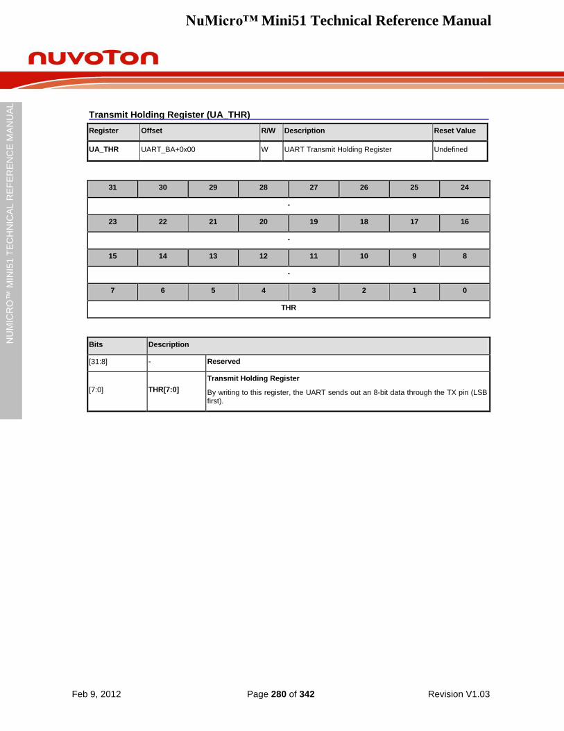
NuMicro™ Mini51 Technical Reference Manual
Feb 9, 2012 Page 280 of 342 Revision V1.03
NU
MIC
RO
™ M
INI5
1 T
EC
HN
ICA
L R
EF
ER
EN
CE
MA
NU
AL
Transmit Holding Register (UA_THR)
Register Offset R/W Description Reset Value
UA_THR UART_BA+0x00 W UART Transmit Holding Register Undefined
31 30 29 28 27 26 25 24
-
23 22 21 20 19 18 17 16
-
15 14 13 12 11 10 9 8
-
7 6 5 4 3 2 1 0
THR
Bits Description
[31:8] - Reserved
[7:0] THR[7:0]
Transmit Holding Register
By writing to this register, the UART sends out an 8-bit data through the TX pin (LSB first).
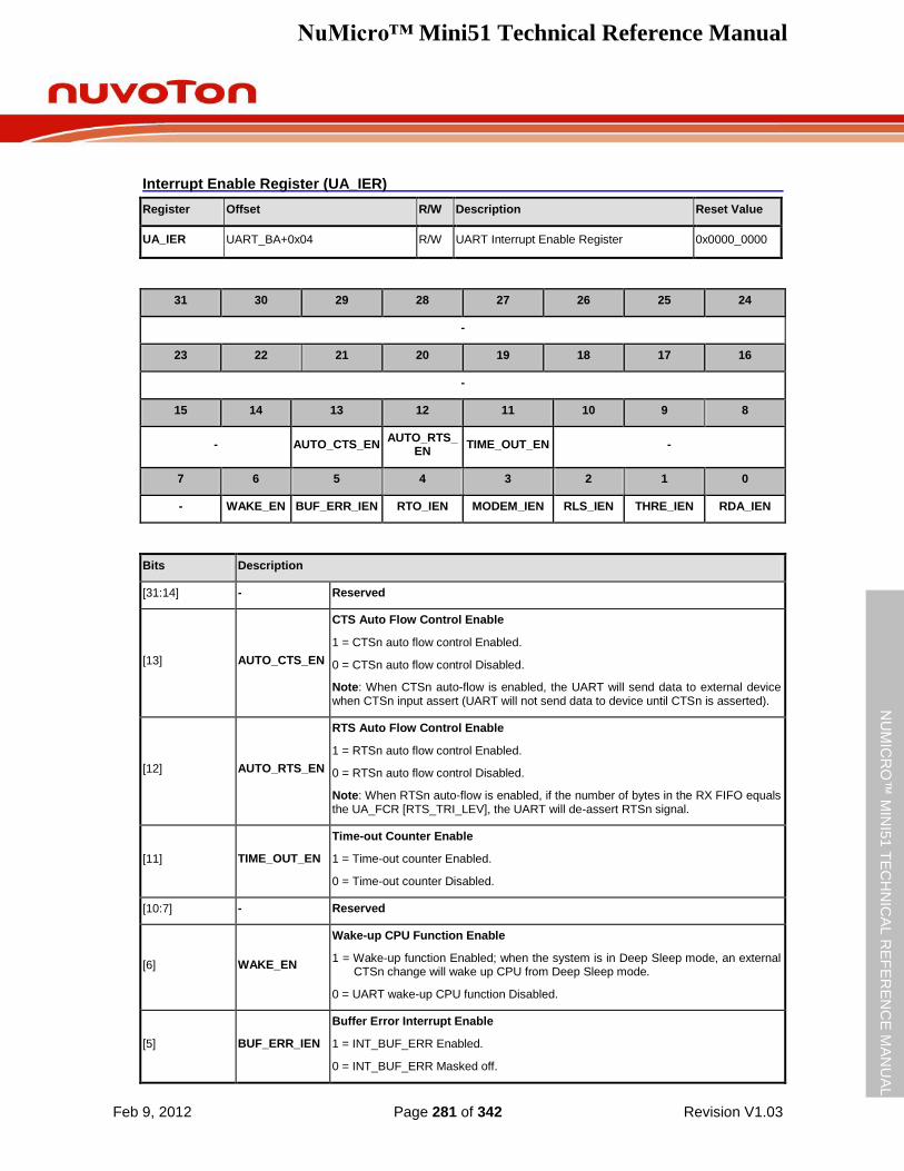
NuMicro™ Mini51 Technical Reference Manual
Feb 9, 2012 Page 281 of 342 Revision V1.03
NU
MIC
RO
™ M
INI5
1 T
EC
HN
ICA
L R
EF
ER
EN
CE
MA
NU
AL
Interrupt Enable Register (UA_IER)
Register Offset R/W Description Reset Value
UA_IER UART_BA+0x04 R/W UART Interrupt Enable Register 0x0000_0000
31 30 29 28 27 26 25 24
-
23 22 21 20 19 18 17 16
-
15 14 13 12 11 10 9 8
- AUTO_CTS_EN AUTO_RTS_
EN TIME_OUT_EN -
7 6 5 4 3 2 1 0
- WAKE_EN BUF_ERR_IEN RTO_IEN MODEM_IEN RLS_IEN THRE_IEN RDA_IEN
Bits Description
[31:14] - Reserved
[13] AUTO_CTS_EN
CTS Auto Flow Control Enable
1 = CTSn auto flow control Enabled.
0 = CTSn auto flow control Disabled.
Note: When CTSn auto-flow is enabled, the UART will send data to external device when CTSn input assert (UART will not send data to device until CTSn is asserted).
[12] AUTO_RTS_EN
RTS Auto Flow Control Enable
1 = RTSn auto flow control Enabled.
0 = RTSn auto flow control Disabled.
Note: When RTSn auto-flow is enabled, if the number of bytes in the RX FIFO equals the UA_FCR [RTS_TRI_LEV], the UART will de-assert RTSn signal.
[11] TIME_OUT_EN
Time-out Counter Enable
1 = Time-out counter Enabled.
0 = Time-out counter Disabled.
[10:7] - Reserved
[6] WAKE_EN
Wake-up CPU Function Enable
1 = Wake-up function Enabled; when the system is in Deep Sleep mode, an external CTSn change will wake up CPU from Deep Sleep mode.
0 = UART wake-up CPU function Disabled.
[5] BUF_ERR_IEN
Buffer Error Interrupt Enable
1 = INT_BUF_ERR Enabled.
0 = INT_BUF_ERR Masked off.
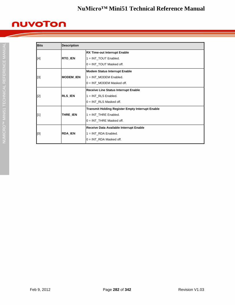
NuMicro™ Mini51 Technical Reference Manual
Feb 9, 2012 Page 282 of 342 Revision V1.03
NU
MIC
RO
™ M
INI5
1 T
EC
HN
ICA
L R
EF
ER
EN
CE
MA
NU
AL
Bits Description
[4] RTO_IEN
RX Time-out Interrupt Enable
1 = INT_TOUT Enabled.
0 = INT_TOUT Masked off.
[3] MODEM_IEN
Modem Status Interrupt Enable
1 = INT_MODEM Enabled.
0 = INT_MODEM Masked off.
[2] RLS_IEN
Receive Line Status Interrupt Enable
1 = INT_RLS Enabled.
0 = INT_RLS Masked off.
[1] THRE_IEN
Transmit Holding Register Empty Interrupt Enable
1 = INT_THRE Enabled.
0 = INT_THRE Masked off.
[0] RDA_IEN
Receive Data Available Interrupt Enable
1 = INT_RDA Enabled.
0 = INT_RDA Masked off.
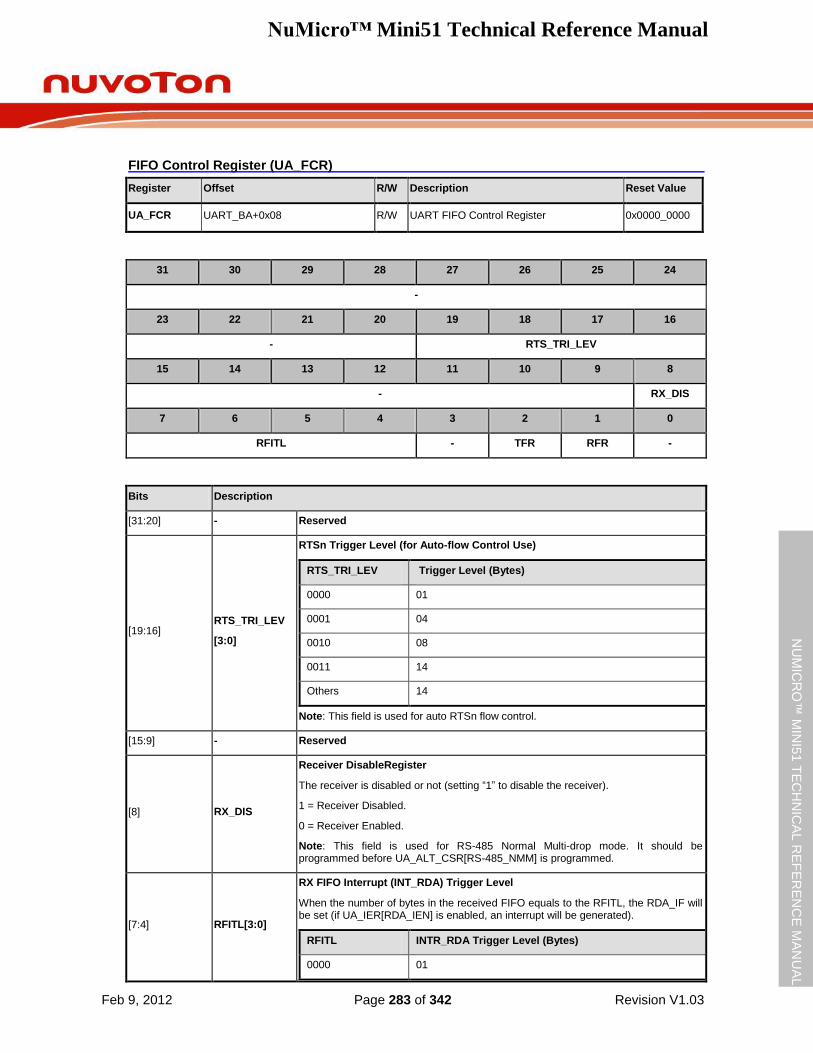
NuMicro™ Mini51 Technical Reference Manual
Feb 9, 2012 Page 283 of 342 Revision V1.03
NU
MIC
RO
™ M
INI5
1 T
EC
HN
ICA
L R
EF
ER
EN
CE
MA
NU
AL
FIFO Control Register (UA_FCR)
Register Offset R/W Description Reset Value
UA_FCR UART_BA+0x08 R/W UART FIFO Control Register 0x0000_0000
31 30 29 28 27 26 25 24
-
23 22 21 20 19 18 17 16
- RTS_TRI_LEV
15 14 13 12 11 10 9 8
- RX_DIS
7 6 5 4 3 2 1 0
RFITL - TFR RFR -
Bits Description
[31:20] - Reserved
[19:16] RTS_TRI_LEV
[3:0]
RTSn Trigger Level (for Auto-flow Control Use)
RTS_TRI_LEV Trigger Level (Bytes)
0000 01
0001 04
0010 08
0011 14
Others 14
Note: This field is used for auto RTSn flow control.
[15:9] - Reserved
[8] RX_DIS
Receiver DisableRegister
The receiver is disabled or not (setting “1” to disable the receiver).
1 = Receiver Disabled.
0 = Receiver Enabled.
Note: This field is used for RS-485 Normal Multi-drop mode. It should be programmed before UA_ALT_CSR[RS-485_NMM] is programmed.
[7:4] RFITL[3:0]
RX FIFO Interrupt (INT_RDA) Trigger Level
When the number of bytes in the received FIFO equals to the RFITL, the RDA_IF will be set (if UA_IER[RDA_IEN] is enabled, an interrupt will be generated).
RFITL INTR_RDA Trigger Level (Bytes)
0000 01

NuMicro™ Mini51 Technical Reference Manual
Feb 9, 2012 Page 284 of 342 Revision V1.03
NU
MIC
RO
™ M
INI5
1 T
EC
HN
ICA
L R
EF
ER
EN
CE
MA
NU
AL
Bits Description
0001 04
0010 08
0011 14
Others 14
[3] - Reserved
[2] TFR
TX Field Software Reset
When TX_RST is set, all the byte in the transmit FIFO and TX internal state machine are cleared.
1 = The TX internal state machine and pointers reset.
0 = No effect.
Note: This bit will auto clear needs at least 3 UART engine clock cycles.
[1] RFR
RX Field Software Reset
When RX_RST is set, all the byte in the receiver FIFO and RX internal state machine are cleared.
1 = The RX internal state machine and pointers reset.
0 = No effect.
Note: This bit will auto clear needs at least 3 UART engine clock cycles.
[0] - Reserved
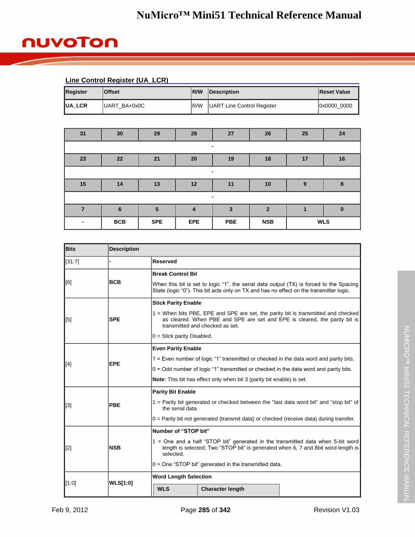
NuMicro™ Mini51 Technical Reference Manual
Feb 9, 2012 Page 285 of 342 Revision V1.03
NU
MIC
RO
™ M
INI5
1 T
EC
HN
ICA
L R
EF
ER
EN
CE
MA
NU
AL
Line Control Register (UA_LCR)
Register Offset R/W Description Reset Value
UA_LCR UART_BA+0x0C R/W UART Line Control Register 0x0000_0000
31 30 29 28 27 26 25 24
-
23 22 21 20 19 18 17 16
-
15 14 13 12 11 10 9 8
-
7 6 5 4 3 2 1 0
- BCB SPE EPE PBE NSB WLS
Bits Description
[31:7] - Reserved
[6] BCB
Break Control Bit
When this bit is set to logic “1”, the serial data output (TX) is forced to the Spacing State (logic “0”). This bit acts only on TX and has no effect on the transmitter logic.
[5] SPE
Stick Parity Enable
1 = When bits PBE, EPE and SPE are set, the parity bit is transmitted and checked as cleared. When PBE and SPE are set and EPE is cleared, the parity bit is transmitted and checked as set.
0 = Stick parity Disabled.
[4] EPE
Even Parity Enable
1 = Even number of logic “1” transmitted or checked in the data word and parity bits.
0 = Odd number of logic “1” transmitted or checked in the data word and parity bits.
Note: This bit has effect only when bit 3 (parity bit enable) is set.
[3] PBE
Parity Bit Enable
1 = Parity bit generated or checked between the "last data word bit" and "stop bit" of the serial data.
0 = Parity bit not generated (transmit data) or checked (receive data) during transfer.
[2] NSB
Number of “STOP bit”
1 = One and a half “STOP bit” generated in the transmitted data when 5-bit word length is selected; Two “STOP bit” is generated when 6, 7 and 8bit word length is selected.
0 = One “STOP bit” generated in the transmitted data.
[1:0] WLS[1:0] Word Length Selection
WLS Character length
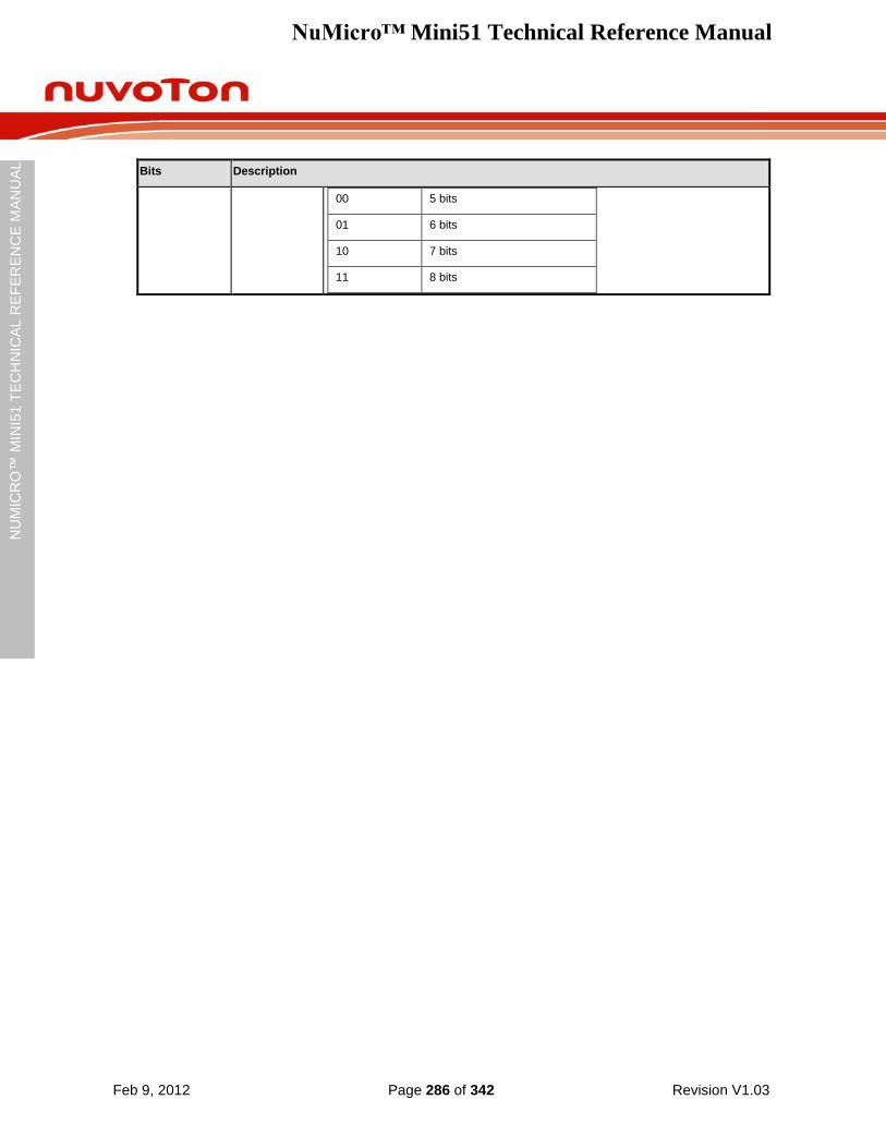
NuMicro™ Mini51 Technical Reference Manual
Feb 9, 2012 Page 286 of 342 Revision V1.03
NU
MIC
RO
™ M
INI5
1 T
EC
HN
ICA
L R
EF
ER
EN
CE
MA
NU
AL
Bits Description
00 5 bits
01 6 bits
10 7 bits
11 8 bits
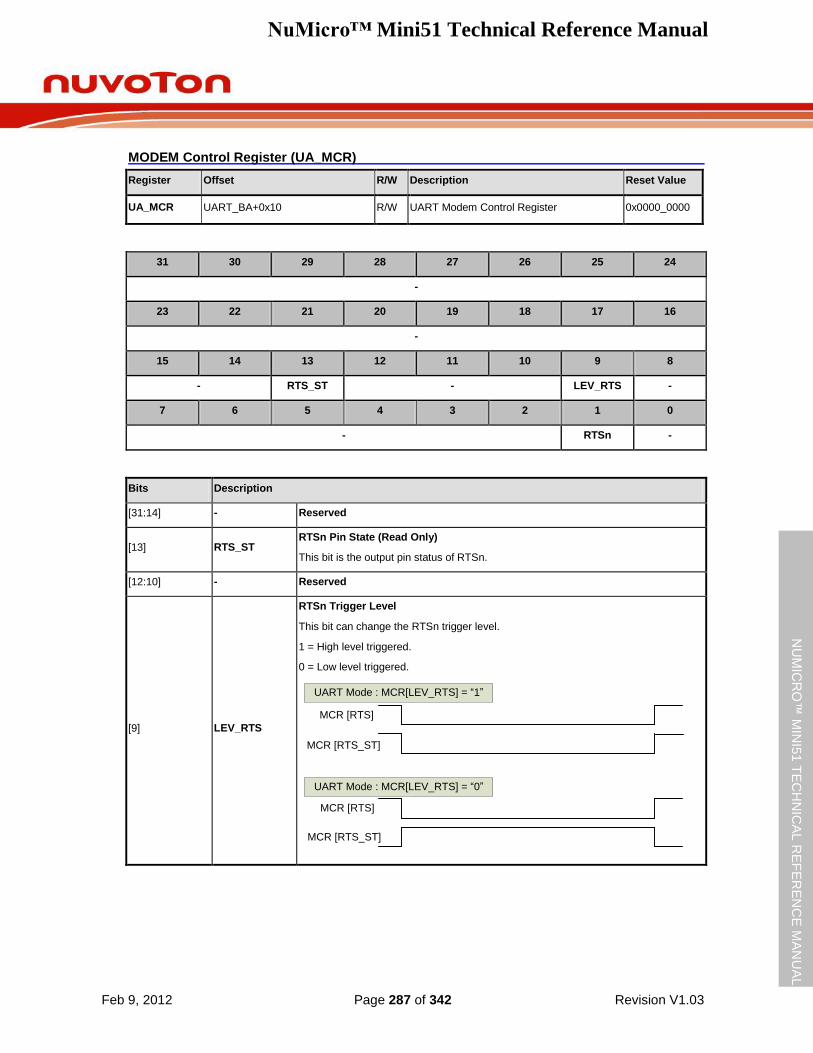
NuMicro™ Mini51 Technical Reference Manual
Feb 9, 2012 Page 287 of 342 Revision V1.03
NU
MIC
RO
™ M
INI5
1 T
EC
HN
ICA
L R
EF
ER
EN
CE
MA
NU
AL
MODEM Control Register (UA_MCR)
Register Offset R/W Description Reset Value
UA_MCR UART_BA+0x10 R/W UART Modem Control Register 0x0000_0000
31 30 29 28 27 26 25 24
-
23 22 21 20 19 18 17 16
-
15 14 13 12 11 10 9 8
- RTS_ST - LEV_RTS -
7 6 5 4 3 2 1 0
- RTSn -
Bits Description
[31:14] - Reserved
[13] RTS_ST RTSn Pin State (Read Only)
This bit is the output pin status of RTSn.
[12:10] - Reserved
[9] LEV_RTS
RTSn Trigger Level
This bit can change the RTSn trigger level.
1 = High level triggered.
0 = Low level triggered.
MCR [RTS_ST]
MCR [RTS]
UART Mode : MCR[LEV_RTS] = “1”
UART Mode : MCR[LEV_RTS] = “0”
MCR [RTS_ST]
MCR [RTS]
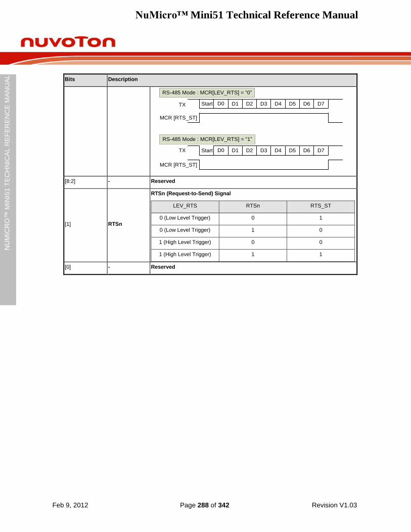
NuMicro™ Mini51 Technical Reference Manual
Feb 9, 2012 Page 288 of 342 Revision V1.03
NU
MIC
RO
™ M
INI5
1 T
EC
HN
ICA
L R
EF
ER
EN
CE
MA
NU
AL
Bits Description
TX
MCR [RTS_ST]
D0TX
MCR [RTS_ST]
RS-485 Mode : MCR[LEV_RTS] = “0”
Start D1 D2 D3 D4 D5 D6 D7
RS-485 Mode : MCR[LEV_RTS] = “1”
D0Start D1 D2 D3 D4 D5 D6 D7
[8:2] - Reserved
[1] RTSn
RTSn (Request-to-Send) Signal
LEV_RTS RTSn RTS_ST
0 (Low Level Trigger) 0 1
0 (Low Level Trigger) 1 0
1 (High Level Trigger) 0 0
1 (High Level Trigger) 1 1
[0] - Reserved
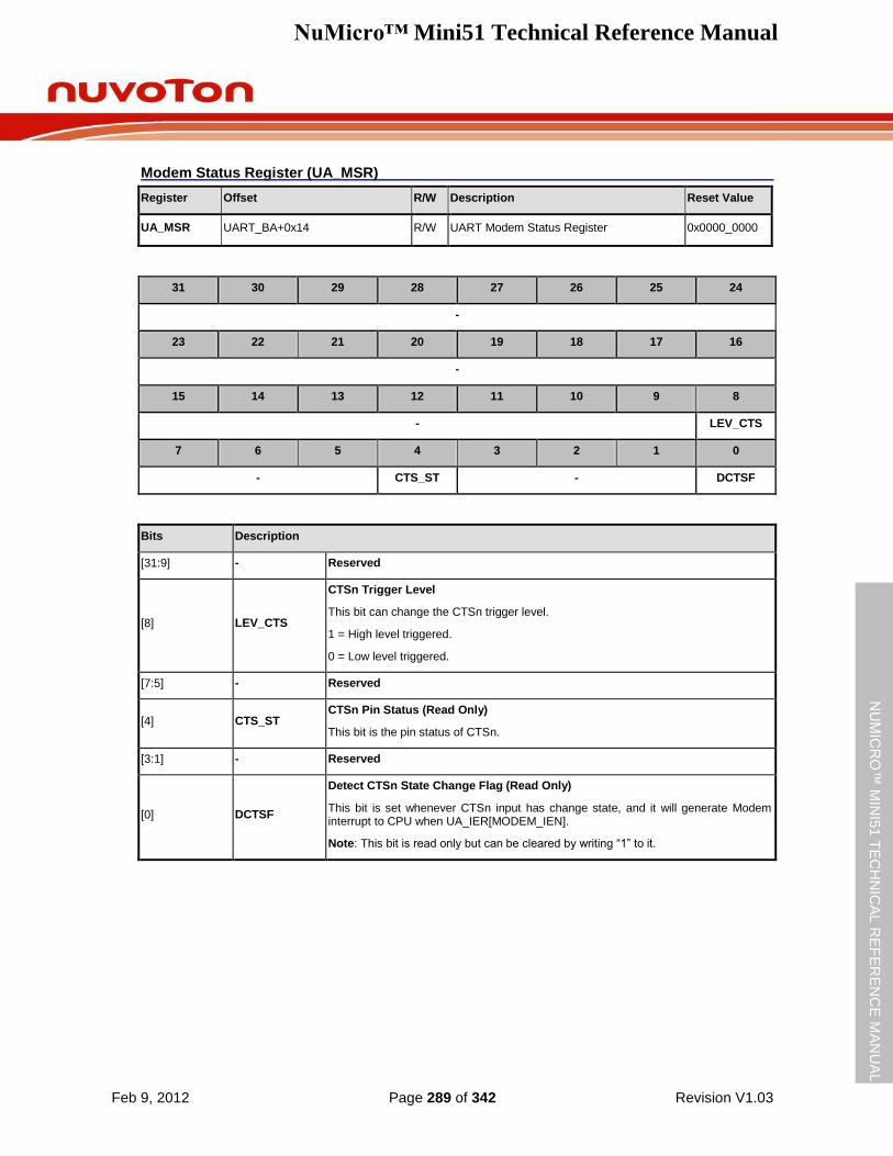
NuMicro™ Mini51 Technical Reference Manual
Feb 9, 2012 Page 289 of 342 Revision V1.03
NU
MIC
RO
™ M
INI5
1 T
EC
HN
ICA
L R
EF
ER
EN
CE
MA
NU
AL
Modem Status Register (UA_MSR)
Register Offset R/W Description Reset Value
UA_MSR UART_BA+0x14 R/W UART Modem Status Register 0x0000_0000
31 30 29 28 27 26 25 24
-
23 22 21 20 19 18 17 16
-
15 14 13 12 11 10 9 8
- LEV_CTS
7 6 5 4 3 2 1 0
- CTS_ST - DCTSF
Bits Description
[31:9] - Reserved
[8] LEV_CTS
CTSn Trigger Level
This bit can change the CTSn trigger level.
1 = High level triggered.
0 = Low level triggered.
[7:5] - Reserved
[4] CTS_ST CTSn Pin Status (Read Only)
This bit is the pin status of CTSn.
[3:1] - Reserved
[0] DCTSF
Detect CTSn State Change Flag (Read Only)
This bit is set whenever CTSn input has change state, and it will generate Modem interrupt to CPU when UA_IER[MODEM_IEN].
Note: This bit is read only but can be cleared by writing “1” to it.
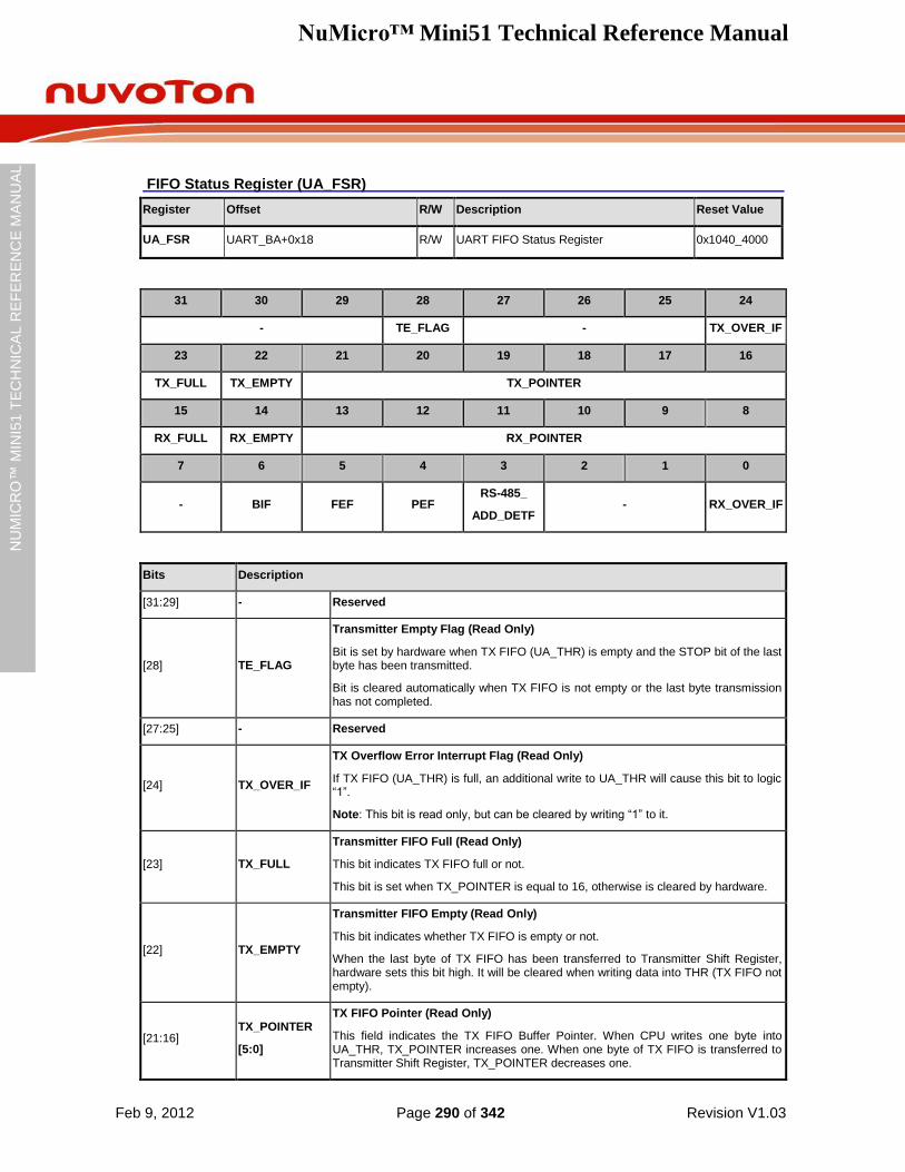
NuMicro™ Mini51 Technical Reference Manual
Feb 9, 2012 Page 290 of 342 Revision V1.03
NU
MIC
RO
™ M
INI5
1 T
EC
HN
ICA
L R
EF
ER
EN
CE
MA
NU
AL
FIFO Status Register (UA_FSR)
Register Offset R/W Description Reset Value
UA_FSR UART_BA+0x18 R/W UART FIFO Status Register 0x1040_4000
31 30 29 28 27 26 25 24
- TE_FLAG - TX_OVER_IF
23 22 21 20 19 18 17 16
TX_FULL TX_EMPTY TX_POINTER
15 14 13 12 11 10 9 8
RX_FULL RX_EMPTY RX_POINTER
7 6 5 4 3 2 1 0
- BIF FEF PEF RS-485_
ADD_DETF - RX_OVER_IF
Bits Description
[31:29] - Reserved
[28] TE_FLAG
Transmitter Empty Flag (Read Only)
Bit is set by hardware when TX FIFO (UA_THR) is empty and the STOP bit of the last byte has been transmitted.
Bit is cleared automatically when TX FIFO is not empty or the last byte transmission has not completed.
[27:25] - Reserved
[24] TX_OVER_IF
TX Overflow Error Interrupt Flag (Read Only)
If TX FIFO (UA_THR) is full, an additional write to UA_THR will cause this bit to logic “1”.
Note: This bit is read only, but can be cleared by writing “1” to it.
[23] TX_FULL
Transmitter FIFO Full (Read Only)
This bit indicates TX FIFO full or not.
This bit is set when TX_POINTER is equal to 16, otherwise is cleared by hardware.
[22] TX_EMPTY
Transmitter FIFO Empty (Read Only)
This bit indicates whether TX FIFO is empty or not.
When the last byte of TX FIFO has been transferred to Transmitter Shift Register, hardware sets this bit high. It will be cleared when writing data into THR (TX FIFO not empty).
[21:16] TX_POINTER
[5:0]
TX FIFO Pointer (Read Only)
This field indicates the TX FIFO Buffer Pointer. When CPU writes one byte into UA_THR, TX_POINTER increases one. When one byte of TX FIFO is transferred to Transmitter Shift Register, TX_POINTER decreases one.
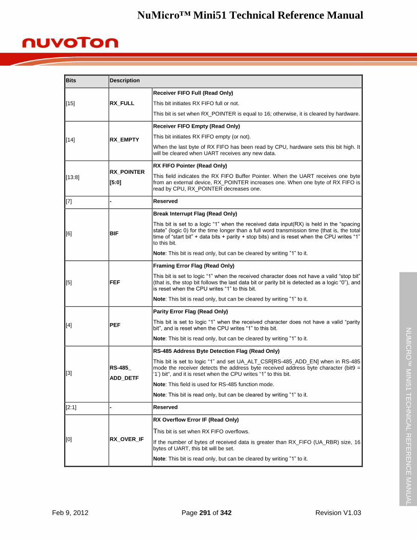
NuMicro™ Mini51 Technical Reference Manual
Feb 9, 2012 Page 291 of 342 Revision V1.03
NU
MIC
RO
™ M
INI5
1 T
EC
HN
ICA
L R
EF
ER
EN
CE
MA
NU
AL
Bits Description
[15] RX_FULL
Receiver FIFO Full (Read Only)
This bit initiates RX FIFO full or not.
This bit is set when RX_POINTER is equal to 16; otherwise, it is cleared by hardware.
[14] RX_EMPTY
Receiver FIFO Empty (Read Only)
This bit initiates RX FIFO empty (or not).
When the last byte of RX FIFO has been read by CPU, hardware sets this bit high. It will be cleared when UART receives any new data.
[13:8] RX_POINTER
[5:0]
RX FIFO Pointer (Read Only)
This field indicates the RX FIFO Buffer Pointer. When the UART receives one byte from an external device, RX_POINTER increases one. When one byte of RX FIFO is read by CPU, RX_POINTER decreases one.
[7] - Reserved
[6] BIF
Break Interrupt Flag (Read Only)
This bit is set to a logic “1” when the received data input(RX) is held in the “spacing state” (logic 0) for the time longer than a full word transmission time (that is, the total time of “start bit” + data bits + parity + stop bits) and is reset when the CPU writes “1” to this bit.
Note: This bit is read only, but can be cleared by writing ”1” to it.
[5] FEF
Framing Error Flag (Read Only)
This bit is set to logic “1” when the received character does not have a valid “stop bit” (that is, the stop bit follows the last data bit or parity bit is detected as a logic “0”), and is reset when the CPU writes “1” to this bit.
Note: This bit is read only, but can be cleared by writing ”1” to it.
[4] PEF
Parity Error Flag (Read Only)
This bit is set to logic “1” when the received character does not have a valid “parity bit”, and is reset when the CPU writes “1” to this bit.
Note: This bit is read only, but can be cleared by writing ”1” to it.
[3] RS-485_
ADD_DETF
RS-485 Address Byte Detection Flag (Read Only)
This bit is set to logic “1” and set UA_ALT_CSR[RS-485_ADD_EN] when in RS-485 mode the receiver detects the address byte received address byte character (bit9 = „1‟) bit", and it is reset when the CPU writes “1” to this bit.
Note: This field is used for RS-485 function mode.
Note: This bit is read only, but can be cleared by writing ”1” to it.
[2:1] - Reserved
[0] RX_OVER_IF
RX Overflow Error IF (Read Only)
This bit is set when RX FIFO overflows.
If the number of bytes of received data is greater than RX_FIFO (UA_RBR) size, 16 bytes of UART, this bit will be set.
Note: This bit is read only, but can be cleared by writing ”1” to it.
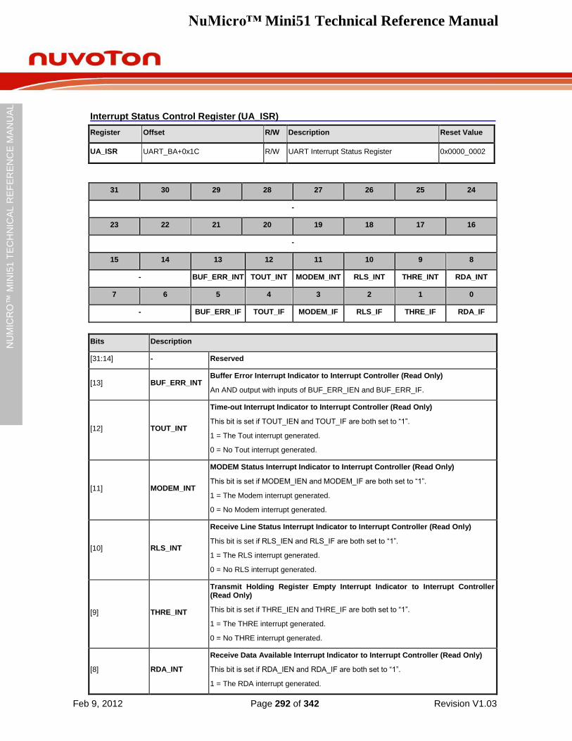
NuMicro™ Mini51 Technical Reference Manual
Feb 9, 2012 Page 292 of 342 Revision V1.03
NU
MIC
RO
™ M
INI5
1 T
EC
HN
ICA
L R
EF
ER
EN
CE
MA
NU
AL
Interrupt Status Control Register (UA_ISR)
Register Offset R/W Description Reset Value
UA_ISR UART_BA+0x1C R/W UART Interrupt Status Register 0x0000_0002
31 30 29 28 27 26 25 24
-
23 22 21 20 19 18 17 16
-
15 14 13 12 11 10 9 8
- BUF_ERR_INT TOUT_INT MODEM_INT RLS_INT THRE_INT RDA_INT
7 6 5 4 3 2 1 0
- BUF_ERR_IF TOUT_IF MODEM_IF RLS_IF THRE_IF RDA_IF
Bits Description
[31:14] - Reserved
[13] BUF_ERR_INT Buffer Error Interrupt Indicator to Interrupt Controller (Read Only)
An AND output with inputs of BUF_ERR_IEN and BUF_ERR_IF.
[12] TOUT_INT
Time-out Interrupt Indicator to Interrupt Controller (Read Only)
This bit is set if TOUT_IEN and TOUT_IF are both set to “1”.
1 = The Tout interrupt generated.
0 = No Tout interrupt generated.
[11] MODEM_INT
MODEM Status Interrupt Indicator to Interrupt Controller (Read Only)
This bit is set if MODEM_IEN and MODEM_IF are both set to “1”.
1 = The Modem interrupt generated.
0 = No Modem interrupt generated.
[10] RLS_INT
Receive Line Status Interrupt Indicator to Interrupt Controller (Read Only)
This bit is set if RLS_IEN and RLS_IF are both set to “1”.
1 = The RLS interrupt generated.
0 = No RLS interrupt generated.
[9] THRE_INT
Transmit Holding Register Empty Interrupt Indicator to Interrupt Controller (Read Only)
This bit is set if THRE_IEN and THRE_IF are both set to “1”.
1 = The THRE interrupt generated.
0 = No THRE interrupt generated.
[8] RDA_INT
Receive Data Available Interrupt Indicator to Interrupt Controller (Read Only)
This bit is set if RDA_IEN and RDA_IF are both set to “1”.
1 = The RDA interrupt generated.
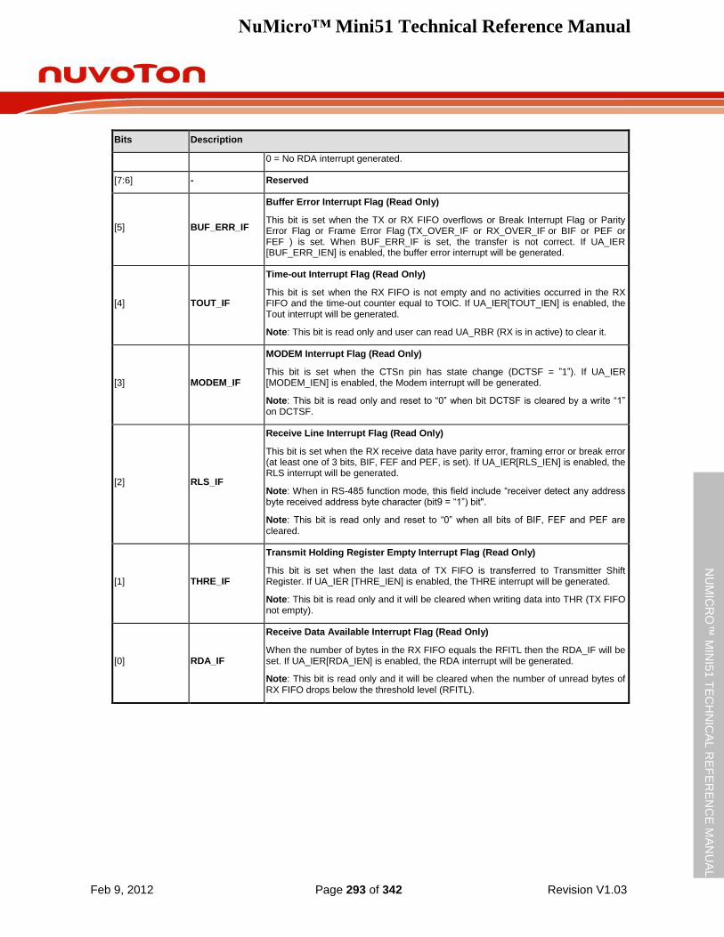
NuMicro™ Mini51 Technical Reference Manual
Feb 9, 2012 Page 293 of 342 Revision V1.03
NU
MIC
RO
™ M
INI5
1 T
EC
HN
ICA
L R
EF
ER
EN
CE
MA
NU
AL
Bits Description
0 = No RDA interrupt generated.
[7:6] - Reserved
[5] BUF_ERR_IF
Buffer Error Interrupt Flag (Read Only)
This bit is set when the TX or RX FIFO overflows or Break Interrupt Flag or Parity Error Flag or Frame Error Flag (TX_OVER_IF or RX_OVER_IF or BIF or PEF or FEF ) is set. When BUF_ERR_IF is set, the transfer is not correct. If UA_IER [BUF_ERR_IEN] is enabled, the buffer error interrupt will be generated.
[4] TOUT_IF
Time-out Interrupt Flag (Read Only)
This bit is set when the RX FIFO is not empty and no activities occurred in the RX FIFO and the time-out counter equal to TOIC. If UA_IER[TOUT_IEN] is enabled, the Tout interrupt will be generated.
Note: This bit is read only and user can read UA_RBR (RX is in active) to clear it.
[3] MODEM_IF
MODEM Interrupt Flag (Read Only)
This bit is set when the CTSn pin has state change (DCTSF = ”1”). If UA_IER [MODEM_IEN] is enabled, the Modem interrupt will be generated.
Note: This bit is read only and reset to “0” when bit DCTSF is cleared by a write “1” on DCTSF.
[2] RLS_IF
Receive Line Interrupt Flag (Read Only)
This bit is set when the RX receive data have parity error, framing error or break error (at least one of 3 bits, BIF, FEF and PEF, is set). If UA_IER[RLS_IEN] is enabled, the RLS interrupt will be generated.
Note: When in RS-485 function mode, this field include “receiver detect any address byte received address byte character (bit9 = “1”) bit".
Note: This bit is read only and reset to “0” when all bits of BIF, FEF and PEF are cleared.
[1] THRE_IF
Transmit Holding Register Empty Interrupt Flag (Read Only)
This bit is set when the last data of TX FIFO is transferred to Transmitter Shift Register. If UA_IER [THRE_IEN] is enabled, the THRE interrupt will be generated.
Note: This bit is read only and it will be cleared when writing data into THR (TX FIFO not empty).
[0] RDA_IF
Receive Data Available Interrupt Flag (Read Only)
When the number of bytes in the RX FIFO equals the RFITL then the RDA_IF will be set. If UA_IER[RDA_IEN] is enabled, the RDA interrupt will be generated.
Note: This bit is read only and it will be cleared when the number of unread bytes of RX FIFO drops below the threshold level (RFITL).
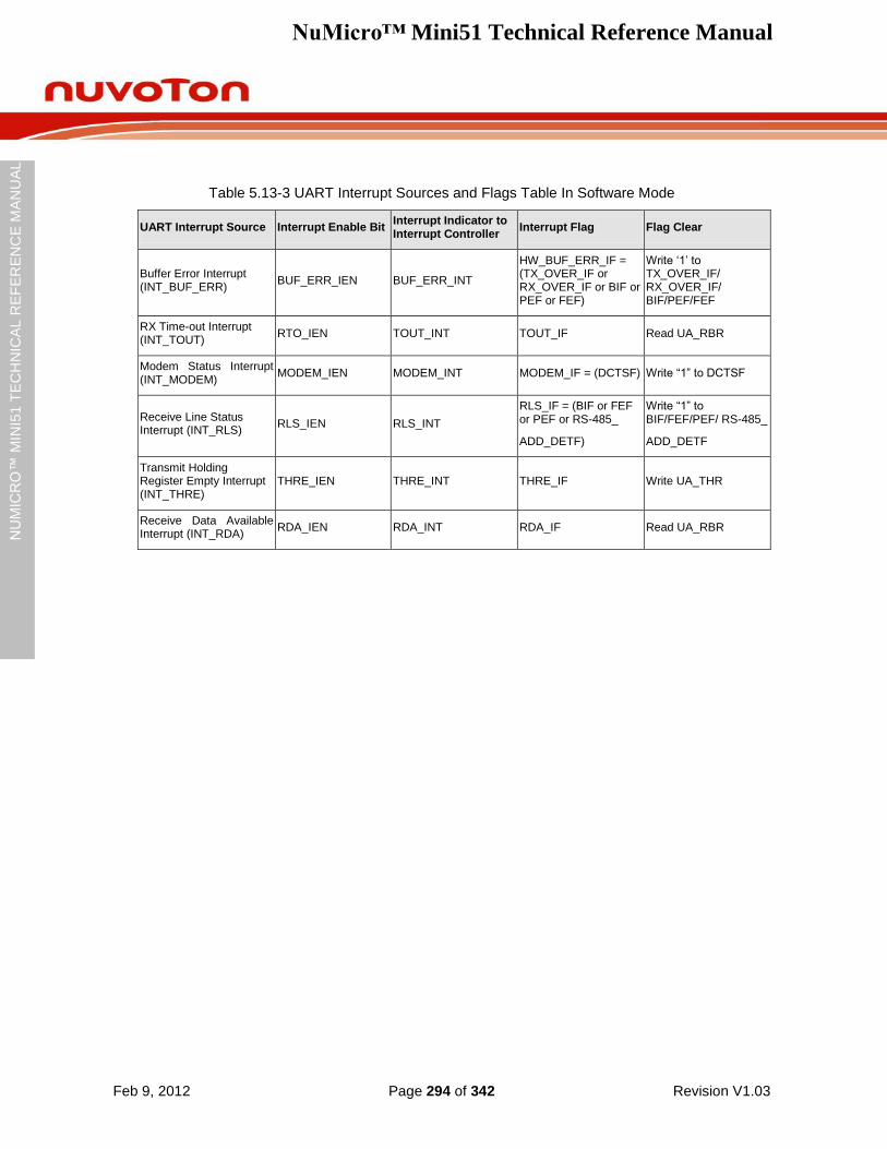
NuMicro™ Mini51 Technical Reference Manual
Feb 9, 2012 Page 294 of 342 Revision V1.03
NU
MIC
RO
™ M
INI5
1 T
EC
HN
ICA
L R
EF
ER
EN
CE
MA
NU
AL
Table 5.13-3 UART Interrupt Sources and Flags Table In Software Mode
UART Interrupt Source Interrupt Enable Bit Interrupt Indicator to Interrupt Controller
Interrupt Flag Flag Clear
Buffer Error Interrupt (INT_BUF_ERR)
BUF_ERR_IEN BUF_ERR_INT
HW_BUF_ERR_IF = (TX_OVER_IF or RX_OVER_IF or BIF or PEF or FEF)
Write „1‟ to TX_OVER_IF/ RX_OVER_IF/ BIF/PEF/FEF
RX Time-out Interrupt (INT_TOUT)
RTO_IEN TOUT_INT TOUT_IF Read UA_RBR
Modem Status Interrupt (INT_MODEM)
MODEM_IEN MODEM_INT MODEM_IF = (DCTSF) Write “1” to DCTSF
Receive Line Status Interrupt (INT_RLS)
RLS_IEN RLS_INT
RLS_IF = (BIF or FEF or PEF or RS-485_
ADD_DETF)
Write “1” to BIF/FEF/PEF/ RS-485_
ADD_DETF
Transmit Holding Register Empty Interrupt (INT_THRE)
THRE_IEN THRE_INT THRE_IF Write UA_THR
Receive Data Available Interrupt (INT_RDA)
RDA_IEN RDA_INT RDA_IF Read UA_RBR
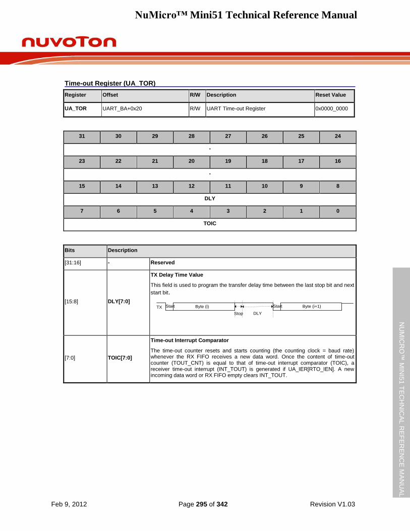
NuMicro™ Mini51 Technical Reference Manual
Feb 9, 2012 Page 295 of 342 Revision V1.03
NU
MIC
RO
™ M
INI5
1 T
EC
HN
ICA
L R
EF
ER
EN
CE
MA
NU
AL
Time-out Register (UA_TOR)
Register Offset R/W Description Reset Value
UA_TOR UART_BA+0x20 R/W UART Time-out Register 0x0000_0000
31 30 29 28 27 26 25 24
-
23 22 21 20 19 18 17 16
-
15 14 13 12 11 10 9 8
DLY
7 6 5 4 3 2 1 0
TOIC
Bits Description
[31:16] - Reserved
[15:8] DLY[7:0]
TX Delay Time Value
This field is used to program the transfer delay time between the last stop bit and next
start bit.
StartTX Byte (i) Byte (i+1)
Stop DLY
Start
[7:0] TOIC[7:0]
Time-out Interrupt Comparator
The time-out counter resets and starts counting (the counting clock = baud rate) whenever the RX FIFO receives a new data word. Once the content of time-out counter (TOUT_CNT) is equal to that of time-out interrupt comparator (TOIC), a receiver time-out interrupt (INT_TOUT) is generated if UA_IER[RTO_IEN]. A new incoming data word or RX FIFO empty clears INT_TOUT.
NuMicro™ Mini51 Technical Reference Manual
Feb 9, 2012 Page 296 of 342 Revision V1.03
NU
MIC
RO
™ M
INI5
1 T
EC
HN
ICA
L R
EF
ER
EN
CE
MA
NU
AL
Baud Rate Divider Register (UA_BAUD)
Register Offset R/W Description Reset Value
UA_BAUD UART_BA+0x24 R/W UART Baud Rate Divisor Register 0x0F00_0000
31 30 29 28 27 26 25 24
- DIV_X_EN DIV_X_ONE DIVIDER_X
23 22 21 20 19 18 17 16
-
15 14 13 12 11 10 9 8
BRD
7 6 5 4 3 2 1 0
BRD
Bits Description
[31:30] - Reserved
[29] DIV_X_EN
Divider X Enable
The BRD = baud rate divider, and the baud rate equation is:Baud Rate = Clock / [M * (BRD + 2)], The default value of M is 16.
1 = The divider X Enabled (the equation of M = X+1, but DIVIDER_X [27:24] must >= 8).
0 = The divider X Disabled (the equation of M = 16).
Refer to the table below for more information.
Note: When in IrDA mode, this bit must be disabled.
[28] DIV_X_ONE
Divider X Equal 1
1 = Divider M = “1” (the equation of M = “1”, but BRD [15:0] must >= 3).
0 = Divider M = “any value” (the equation of M = X+1, but DIVIDER_X[27:24] must >= 8).
Refer to the table below for more information.
[27:24] DIVIDER_X[3:0] Divider X
The baud rate divider M = X+1.
[23:16] - Reserved
[15:0] BRD[15:0] Baud Rate Divider
The field indicates the baud rate divider.
NuMicro™ Mini51 Technical Reference Manual
Feb 9, 2012 Page 297 of 342 Revision V1.03
NU
MIC
RO
™ M
INI5
1 T
EC
HN
ICA
L R
EF
ER
EN
CE
MA
NU
AL
Table 5.13-4 UART Baud Rate Setting Table
Mode DIV_X_EN DIV_X_ONE Divider X BRD Baud Rate Equation
0 0 0 B A UART_CLK / [16 * (A+2)]
1 1 0 B A UART_CLK / [(B+1) * (A+2)] , B must >= 8
2 1 1 Don‟t care A UART_CLK / (A+2), A must >=3
NuMicro™ Mini51 Technical Reference Manual
Feb 9, 2012 Page 298 of 342 Revision V1.03
NU
MIC
RO
™ M
INI5
1 T
EC
HN
ICA
L R
EF
ER
EN
CE
MA
NU
AL
IrDA Control Register (IRCR)
Register Offset R/W Description Reset Value
UA_IRCR UART_BA+0x28 R/W UART IrDA Control Register 0x0000_0040
31 30 29 28 27 26 25 24
-
23 22 21 20 19 18 17 16
-
15 14 13 12 11 10 9 8
-
7 6 5 4 3 2 1 0
- INV_RX INV_TX - TX_SELECT -
Bits Description
[31:7] - Reserved
[6] INV_RX
INV_RX
1 = RX input signal inversed.
0 = No inversion.
[5] INV_TX
INV_TX
1 = TX output signal inversed.
0 = No inversion.
[4:2] - Reserved
[1] TX_SELECT
TX_SELECT
1 = IrDA transmitter Enabled.
0 = IrDA receiver Enabled.
Note: When in IrDA mode, the UA_BAUD[DIV_X_EN] register must be disabled (the baud equation must be Clock / 16 * (BRD).
[0] - Reserved
NuMicro™ Mini51 Technical Reference Manual
Feb 9, 2012 Page 299 of 342 Revision V1.03
NU
MIC
RO
™ M
INI5
1 T
EC
HN
ICA
L R
EF
ER
EN
CE
MA
NU
AL
UART Alternate Control/Status Register (UA_ALT_CSR)
Register Offset R/W Description Reset Value
UA_ALT_CSR UART_BA+0x2C R/W UART Alternate Control/Status Register 0x0000_0000
31 30 29 28 27 26 25 24
ADDR_MATCH
23 22 21 20 19 18 17 16
-
15 14 13 12 11 10 9 8
RS485_ADD_EN
- RS485_AUD RS485_AAD RS485_NMM
7 6 5 4 3 2 1 0
-
Bits Description
[31:24] ADDR_MATCH
[7:0]
Address Match Value Register
This field contains the RS-485 address match values.
Note: This field is used for Auto RS-485 Address Detection mode.
[23:16] - Reserved
[15] RS485_ADD_EN
RS-485 Address Detection Enable
This bit is use to enable RS-485 Address Detection mode.
1 = Address Detection mode Enabled.
0 = Address Detection mode Disabled.
Note: This field is used for any RS-485 Operation mode.
[14:11] - Reserved
[10] RS485_AUD
RS-485 Auto Direction Mode (AUD)
1 = RS-485 Auto Direction Operation mode (AUD) Enabled.
0 = RS-485 Auto Direction Operation mode (AUD) Disabled.
Note: It is able to be active in RS-485_AAD or RS-485_NMM Operation mode.
[9] RS485_AAD
RS-485 Auto Address Detection Operation Mode (AAD)
1 = RS-485 Auto Address Detection Operation mode (AAD) Enabled.
0 = RS-485 Auto Address Detection Operation mode (AAD) Disabled.
Note: It is unable to be active in RS-485_NMM Operation mode.
[8] RS485_NMM
RS-485 Normal Multi-drop Operation Mode (NMM)
1 = RS-485 Normal Multi-drop Operation mode (NMM) Enabled.
0 = RS-485 Normal Multi-drop Operation mode (NMM) Disabled.
Note: It is unable to be active in RS-485_AAD Operation mode.
NuMicro™ Mini51 Technical Reference Manual
Feb 9, 2012 Page 300 of 342 Revision V1.03
NU
MIC
RO
™ M
INI5
1 T
EC
HN
ICA
L R
EF
ER
EN
CE
MA
NU
AL
Bits Description
[7:0] - Reserved
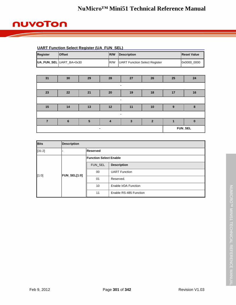
NuMicro™ Mini51 Technical Reference Manual
Feb 9, 2012 Page 301 of 342 Revision V1.03
NU
MIC
RO
™ M
INI5
1 T
EC
HN
ICA
L R
EF
ER
EN
CE
MA
NU
AL
UART Function Select Register (UA_FUN_SEL)
Register Offset R/W Description Reset Value
UA_FUN_SEL UART_BA+0x30 R/W UART Function Select Register 0x0000_0000
31 30 29 28 27 26 25 24
-
23 22 21 20 19 18 17 16
-
15 14 13 12 11 10 9 8
-
7 6 5 4 3 2 1 0
- FUN_SEL
Bits Description
[31:2] - Reserved
[1:0] FUN_SEL[1:0]
Function Select Enable
FUN_SEL Description
00 UART Function
01 Reserved.
10 Enable IrDA Function
11 Enable RS-485 Function
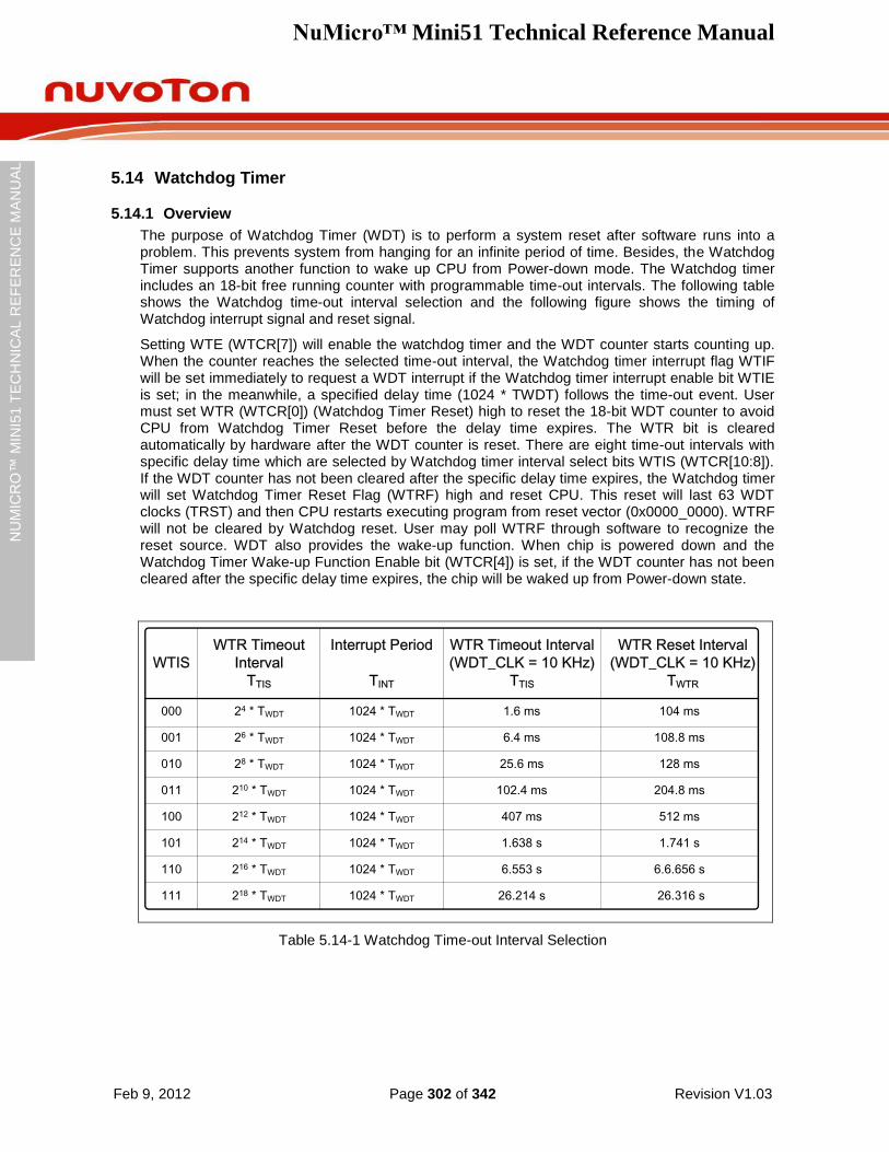
NuMicro™ Mini51 Technical Reference Manual
Feb 9, 2012 Page 302 of 342 Revision V1.03
NU
MIC
RO
™ M
INI5
1 T
EC
HN
ICA
L R
EF
ER
EN
CE
MA
NU
AL
5.14 Watchdog Timer
5.14.1 Overview
The purpose of Watchdog Timer (WDT) is to perform a system reset after software runs into a problem. This prevents system from hanging for an infinite period of time. Besides, the Watchdog Timer supports another function to wake up CPU from Power-down mode. The Watchdog timer includes an 18-bit free running counter with programmable time-out intervals. The following table shows the Watchdog time-out interval selection and the following figure shows the timing of Watchdog interrupt signal and reset signal.
Setting WTE (WTCR[7]) will enable the watchdog timer and the WDT counter starts counting up. When the counter reaches the selected time-out interval, the Watchdog timer interrupt flag WTIF will be set immediately to request a WDT interrupt if the Watchdog timer interrupt enable bit WTIE is set; in the meanwhile, a specified delay time (1024 * TWDT) follows the time-out event. User must set WTR (WTCR[0]) (Watchdog Timer Reset) high to reset the 18-bit WDT counter to avoid CPU from Watchdog Timer Reset before the delay time expires. The WTR bit is cleared automatically by hardware after the WDT counter is reset. There are eight time-out intervals with specific delay time which are selected by Watchdog timer interval select bits WTIS (WTCR[10:8]). If the WDT counter has not been cleared after the specific delay time expires, the Watchdog timer will set Watchdog Timer Reset Flag (WTRF) high and reset CPU. This reset will last 63 WDT clocks (TRST) and then CPU restarts executing program from reset vector (0x0000_0000). WTRF will not be cleared by Watchdog reset. User may poll WTRF through software to recognize the reset source. WDT also provides the wake-up function. When chip is powered down and the Watchdog Timer Wake-up Function Enable bit (WTCR[4]) is set, if the WDT counter has not been cleared after the specific delay time expires, the chip will be waked up from Power-down state.
WTR Timeout
Interval
TTIS
WTIS
WTR Timeout Interval
(WDT_CLK = 10 KHz)
TTIS
000
216 * TWDT
218 * TWDT 1024 * TWDT
Interrupt Period
TINT
26.214 s
6.553 s
1.638 s
407 ms
102.4 ms
25.6 ms
6.4 ms
1.6 ms
1024 * TWDT
1024 * TWDT
1024 * TWDT
1024 * TWDT
1024 * TWDT
1024 * TWDT
1024 * TWDT
214 * TWDT
212 * TWDT
210 * TWDT
28 * TWDT
26 * TWDT
24 * TWDT
001
010
011
100
101
110
111
WTR Reset Interval
(WDT_CLK = 10 KHz)
TWTR
26.316 s
6.6.656 s
1.741 s
512 ms
204.8 ms
128 ms
108.8 ms
104 ms
Table 5.14-1 Watchdog Time-out Interval Selection
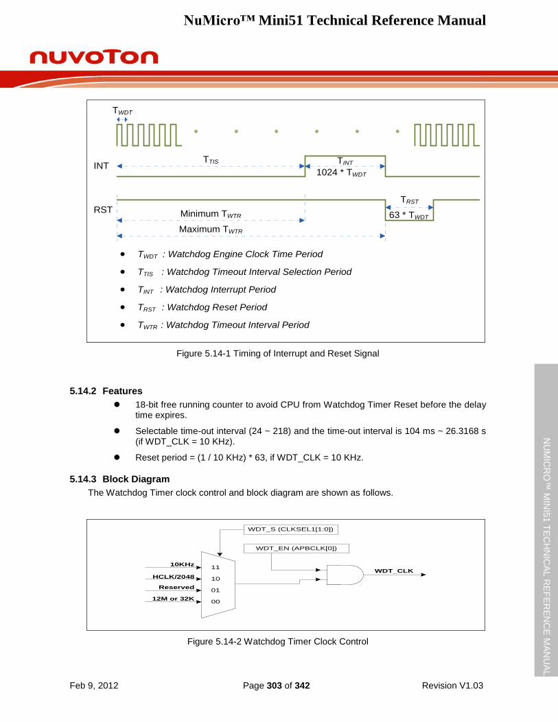
NuMicro™ Mini51 Technical Reference Manual
Feb 9, 2012 Page 303 of 342 Revision V1.03
NU
MIC
RO
™ M
INI5
1 T
EC
HN
ICA
L R
EF
ER
EN
CE
MA
NU
AL
TTIS
RST
INT 1024 * TWDT
63 * TWDTMinimum TWTR
TINT
TRST
Maximum TWTR
TWDT
TWDT : Watchdog Engine Clock Time Period
TTIS : Watchdog Timeout Interval Selection Period
TINT : Watchdog Interrupt Period
TRST : Watchdog Reset Period
TWTR : Watchdog Timeout Interval Period
Figure 5.14-1 Timing of Interrupt and Reset Signal
5.14.2 Features
18-bit free running counter to avoid CPU from Watchdog Timer Reset before the delay time expires.
Selectable time-out interval (24 ~ 218) and the time-out interval is 104 ms ~ 26.3168 s (if WDT_CLK = 10 KHz).
Reset period = (1 / 10 KHz) * 63, if WDT_CLK = 10 KHz.
5.14.3 Block Diagram
The Watchdog Timer clock control and block diagram are shown as follows.
11
10
01
00
HCLK/2048
Reserved
12M or 32K
10KHz
WDT_S (CLKSEL1[1:0])
WDT_EN (APBCLK[0])
WDT_CLK
Figure 5.14-2 Watchdog Timer Clock Control
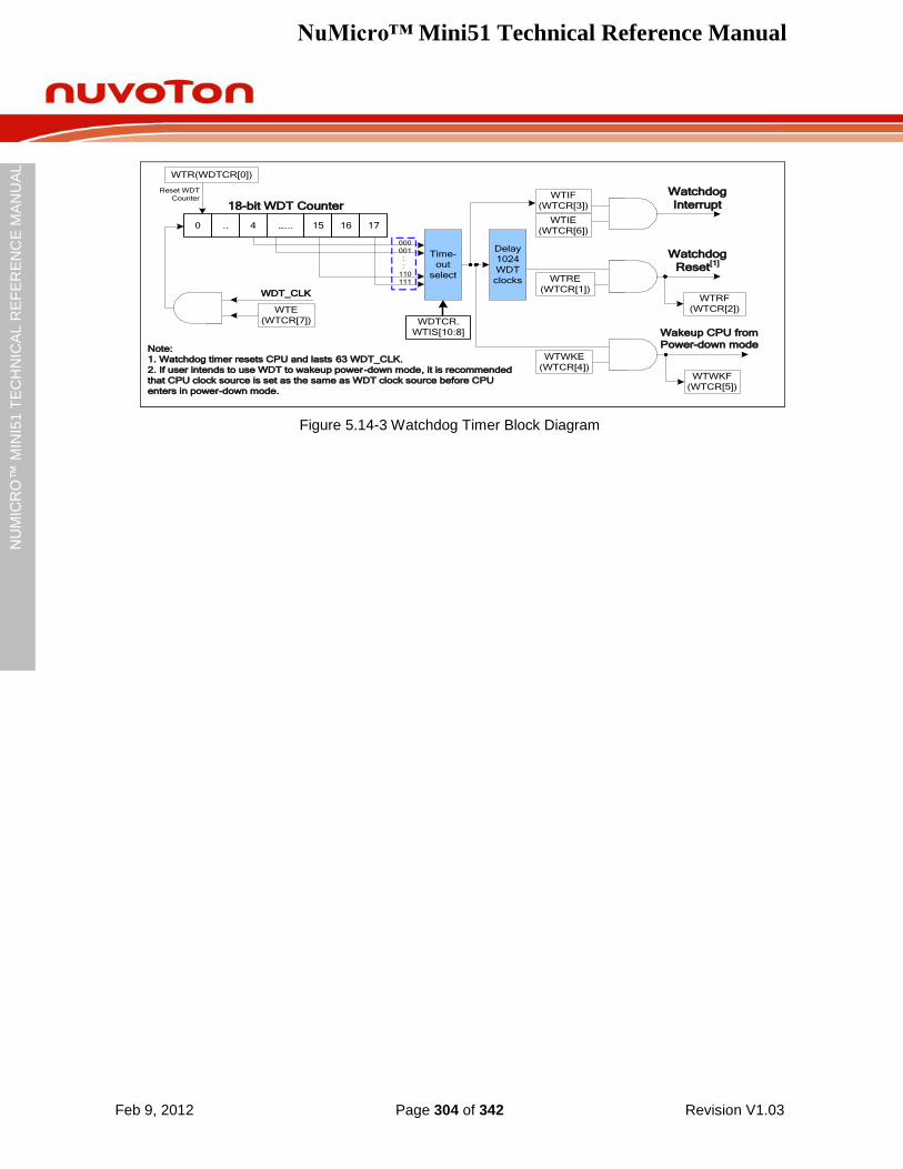
NuMicro™ Mini51 Technical Reference Manual
Feb 9, 2012 Page 304 of 342 Revision V1.03
NU
MIC
RO
™ M
INI5
1 T
EC
HN
ICA
L R
EF
ER
EN
CE
MA
NU
AL
18-bit WDT Counter
0 …... 15.. 4 16 17
000
001
110
111
:
:
WDT_CLK
Time-
out
select
Delay
1024
WDT
clocks
Watchdog
Interrupt
WTRE
(WTCR[1])
Watchdog
Reset[1]
WTR(WDTCR[0])
Reset WDT
Counter
Note:
1. Watchdog timer resets CPU and lasts 63 WDT_CLK.
2. If user intends to use WDT to wakeup power-down mode, it is recommended
that CPU clock source is set as the same as WDT clock source before CPU
enters in power-down mode.
WTIE
(WTCR[6])
WTE
(WTCR[7])
WTIF
(WTCR[3])
WTRF
(WTCR[2])
WDTCR.
WTIS[10:8] Wakeup CPU from
Power-down mode
WTWKE
(WTCR[4])WTWKF
(WTCR[5])
Figure 5.14-3 Watchdog Timer Block Diagram
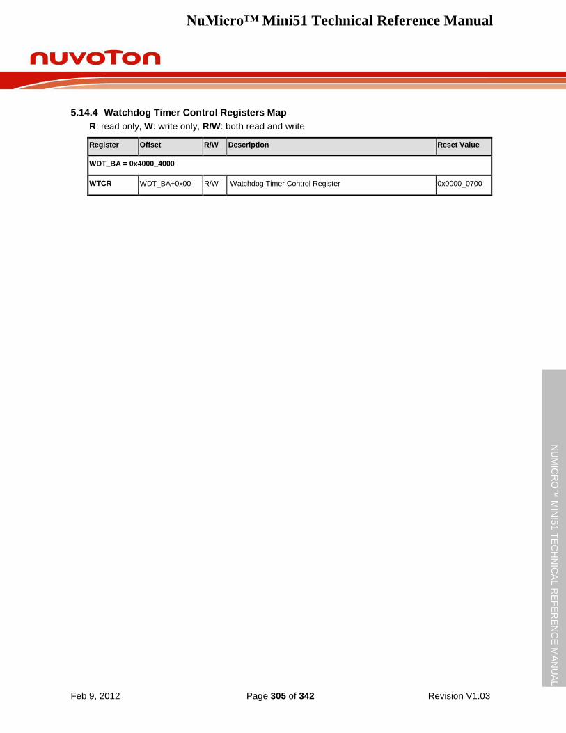
NuMicro™ Mini51 Technical Reference Manual
Feb 9, 2012 Page 305 of 342 Revision V1.03
NU
MIC
RO
™ M
INI5
1 T
EC
HN
ICA
L R
EF
ER
EN
CE
MA
NU
AL
5.14.4 Watchdog Timer Control Registers Map
R: read only, W: write only, R/W: both read and write
Register Offset R/W Description Reset Value
WDT_BA = 0x4000_4000
WTCR WDT_BA+0x00 R/W Watchdog Timer Control Register 0x0000_0700
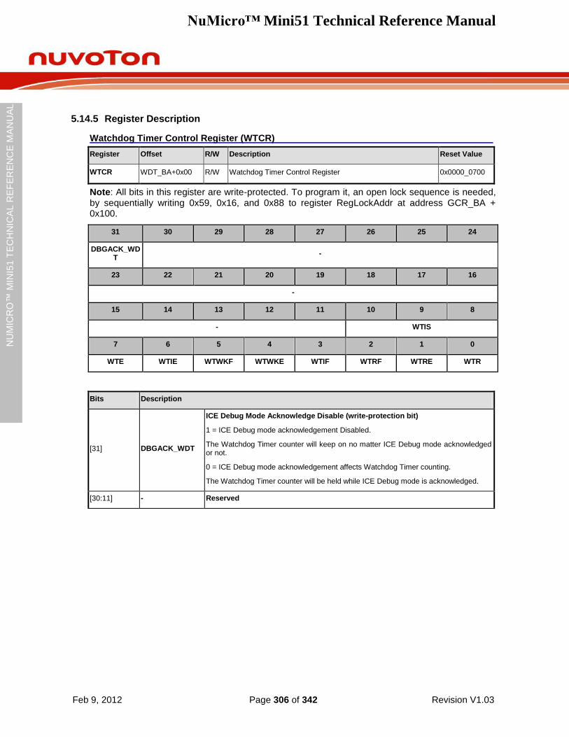
NuMicro™ Mini51 Technical Reference Manual
Feb 9, 2012 Page 306 of 342 Revision V1.03
NU
MIC
RO
™ M
INI5
1 T
EC
HN
ICA
L R
EF
ER
EN
CE
MA
NU
AL
5.14.5 Register Description
Watchdog Timer Control Register (WTCR)
Register Offset R/W Description Reset Value
WTCR WDT_BA+0x00 R/W Watchdog Timer Control Register 0x0000_0700
Note: All bits in this register are write-protected. To program it, an open lock sequence is needed, by sequentially writing 0x59, 0x16, and 0x88 to register RegLockAddr at address GCR_BA + 0x100.
31 30 29 28 27 26 25 24
DBGACK_WDT
-
23 22 21 20 19 18 17 16
-
15 14 13 12 11 10 9 8
- WTIS
7 6 5 4 3 2 1 0
WTE WTIE WTWKF WTWKE WTIF WTRF WTRE WTR
Bits Description
[31] DBGACK_WDT
ICE Debug Mode Acknowledge Disable (write-protection bit)
1 = ICE Debug mode acknowledgement Disabled.
The Watchdog Timer counter will keep on no matter ICE Debug mode acknowledged or not.
0 = ICE Debug mode acknowledgement affects Watchdog Timer counting.
The Watchdog Timer counter will be held while ICE Debug mode is acknowledged.
[30:11] - Reserved
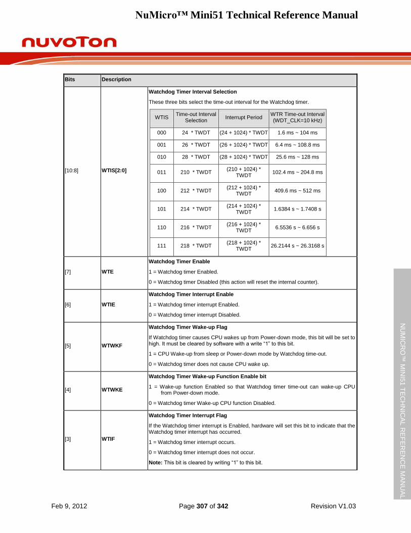
NuMicro™ Mini51 Technical Reference Manual
Feb 9, 2012 Page 307 of 342 Revision V1.03
NU
MIC
RO
™ M
INI5
1 T
EC
HN
ICA
L R
EF
ER
EN
CE
MA
NU
AL
Bits Description
[10:8] WTIS[2:0]
Watchdog Timer Interval Selection
These three bits select the time-out interval for the Watchdog timer.
WTIS Time-out Interval
Selection Interrupt Period
WTR Time-out Interval (WDT_CLK=10 kHz)
000 24 * TWDT (24 + 1024) * TWDT 1.6 ms ~ 104 ms
001 26 * TWDT (26 + 1024) * TWDT 6.4 ms ~ 108.8 ms
010 28 * TWDT (28 + 1024) * TWDT 25.6 ms ~ 128 ms
011 210 * TWDT (210 + 1024) *
TWDT 102.4 ms ~ 204.8 ms
100 212 * TWDT (212 + 1024) *
TWDT 409.6 ms ~ 512 ms
101 214 * TWDT (214 + 1024) *
TWDT 1.6384 s ~ 1.7408 s
110 216 * TWDT (216 + 1024) *
TWDT 6.5536 s ~ 6.656 s
111 218 * TWDT (218 + 1024) *
TWDT 26.2144 s ~ 26.3168 s
[7] WTE
Watchdog Timer Enable
1 = Watchdog timer Enabled.
0 = Watchdog timer Disabled (this action will reset the internal counter).
[6] WTIE
Watchdog Timer Interrupt Enable
1 = Watchdog timer interrupt Enabled.
0 = Watchdog timer interrupt Disabled.
[5] WTWKF
Watchdog Timer Wake-up Flag
If Watchdog timer causes CPU wakes up from Power-down mode, this bit will be set to high. It must be cleared by software with a write “1” to this bit.
1 = CPU Wake-up from sleep or Power-down mode by Watchdog time-out.
0 = Watchdog timer does not cause CPU wake up.
[4] WTWKE
Watchdog Timer Wake-up Function Enable bit
1 = Wake-up function Enabled so that Watchdog timer time-out can wake-up CPU from Power-down mode.
0 = Watchdog timer Wake-up CPU function Disabled.
[3] WTIF
Watchdog Timer Interrupt Flag
If the Watchdog timer interrupt is Enabled, hardware will set this bit to indicate that the Watchdog timer interrupt has occurred.
1 = Watchdog timer interrupt occurs.
0 = Watchdog timer interrupt does not occur.
Note: This bit is cleared by writing “1” to this bit.
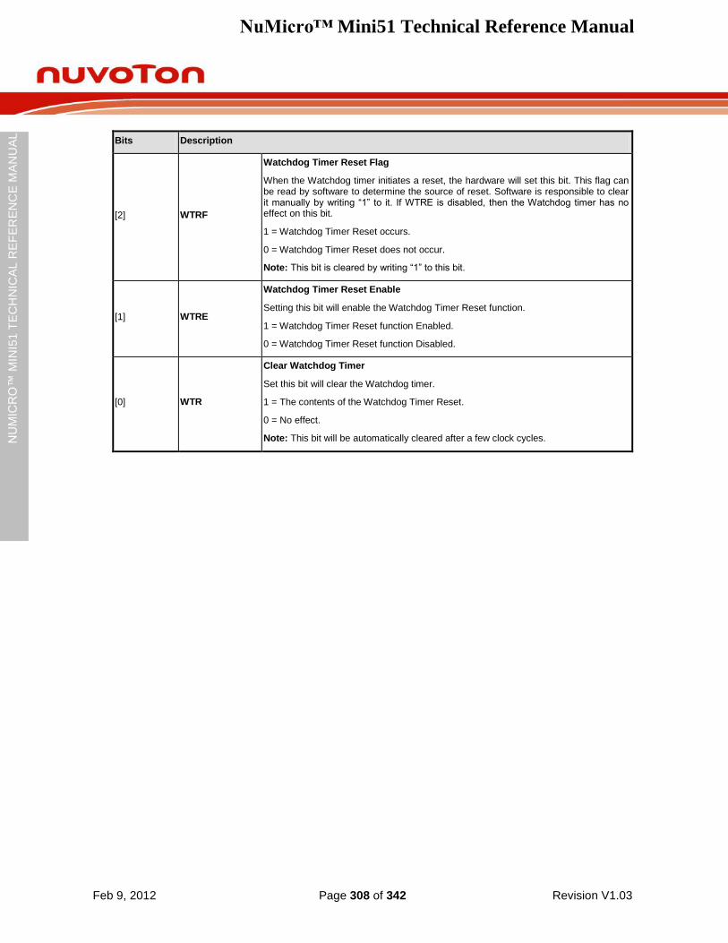
NuMicro™ Mini51 Technical Reference Manual
Feb 9, 2012 Page 308 of 342 Revision V1.03
NU
MIC
RO
™ M
INI5
1 T
EC
HN
ICA
L R
EF
ER
EN
CE
MA
NU
AL
Bits Description
[2] WTRF
Watchdog Timer Reset Flag
When the Watchdog timer initiates a reset, the hardware will set this bit. This flag can be read by software to determine the source of reset. Software is responsible to clear it manually by writing “1” to it. If WTRE is disabled, then the Watchdog timer has no effect on this bit.
1 = Watchdog Timer Reset occurs.
0 = Watchdog Timer Reset does not occur.
Note: This bit is cleared by writing “1” to this bit.
[1] WTRE
Watchdog Timer Reset Enable
Setting this bit will enable the Watchdog Timer Reset function.
1 = Watchdog Timer Reset function Enabled.
0 = Watchdog Timer Reset function Disabled.
[0] WTR
Clear Watchdog Timer
Set this bit will clear the Watchdog timer.
1 = The contents of the Watchdog Timer Reset.
0 = No effect.
Note: This bit will be automatically cleared after a few clock cycles.
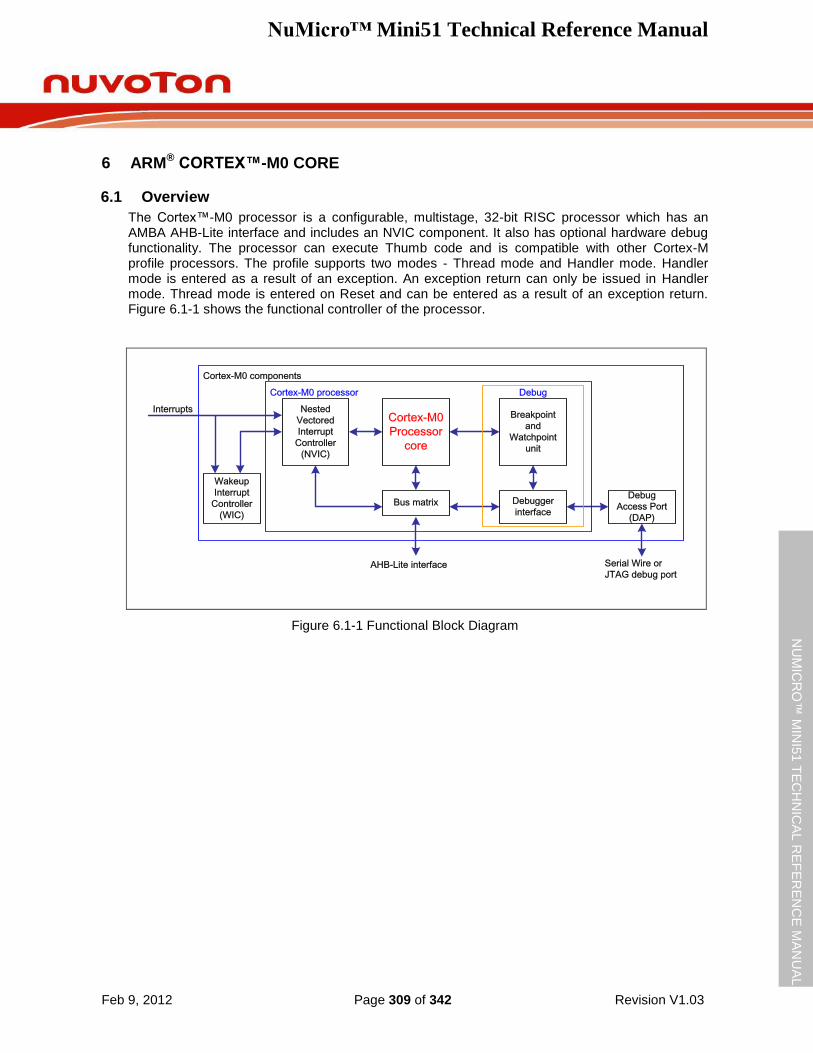
NuMicro™ Mini51 Technical Reference Manual
Feb 9, 2012 Page 309 of 342 Revision V1.03
NU
MIC
RO
™ M
INI5
1 T
EC
HN
ICA
L R
EF
ER
EN
CE
MA
NU
AL
6 ARM® CORTEX™-M0 CORE
6.1 Overview
The Cortex™-M0 processor is a configurable, multistage, 32-bit RISC processor which has an AMBA AHB-Lite interface and includes an NVIC component. It also has optional hardware debug functionality. The processor can execute Thumb code and is compatible with other Cortex-M profile processors. The profile supports two modes - Thread mode and Handler mode. Handler mode is entered as a result of an exception. An exception return can only be issued in Handler mode. Thread mode is entered on Reset and can be entered as a result of an exception return. Figure 6.1-1 shows the functional controller of the processor.
Cortex-M0
Processor
core
Nested
Vectored
Interrupt
Controller
(NVIC)
Breakpoint
and
Watchpoint
unit
Debugger
interfaceBus matrix
Debug
Access Port
(DAP)
DebugCortex-M0 processor
Cortex-M0 components
Wakeup
Interrupt
Controller
(WIC)
Interrupts
Serial Wire or
JTAG debug portAHB-Lite interface
Figure 6.1-1 Functional Block Diagram

NuMicro™ Mini51 Technical Reference Manual
Feb 9, 2012 Page 310 of 342 Revision V1.03
NU
MIC
RO
™ M
INI5
1 T
EC
HN
ICA
L R
EF
ER
EN
CE
MA
NU
AL
6.2 Features
A low gate count processor
ARMv6-M Thumb® instruction set
Thumb-2 technology
ARMv6-M compliant 24-bit SysTick timer
A 32-bit hardware multiplier
Supports little-endian data accesses
Deterministic, fixed-latency, interrupt handling
Load/store-multiples and multicycle-multiplies that can be abandoned and restarted to facilitate rapid interrupt handling
C Application Binary Interface compliant exception model:
ARMv6-M, C Application Binary Interface (C-ABI) compliant exception model that enables the use of pure C functions as interrupt handlers
Low power Idle mode entry using Wait For Interrupt (WFI), Wait For Event (WFE) instructions, or the return from interrupt sleep-on-exit feature
NVIC
32 external interrupt inputs, each with four levels of priority
Dedicated Non-Maskable Interrupt (NMI) input
Supports both level-sensitive and pulse-sensitive interrupt lines
Wake-up Interrupt Controller (WIC) with ultra-low power Idle mode support
Debug support
Four hardware breakpoints
Two watchpoints
Program Counter Sampling Register (PCSR) for non-intrusive code profiling
Single step and vector catch capabilities
Bus interfaces
Single 32-bit AMBA-3 AHB-Lite system interface that provides simple integration to all system peripherals and memory
Single 32-bit slave port that supports the Debug Access Port DAP (DAP)
NuMicro™ Mini51 Technical Reference Manual
Feb 9, 2012 Page 311 of 342 Revision V1.03
NU
MIC
RO
™ M
INI5
1 T
EC
HN
ICA
L R
EF
ER
EN
CE
MA
NU
AL
6.3 System Timer (SysTick)
The Cortex-M0 includes an integrated system timer, SysTick, which provides a simple, 24-bit clear-on-write, decrementing, wrap-on-zero counter with a flexible control mechanism. The counter can be used as a Real Time Operating System (RTOS) tick timer or as a simple counter.
When system timer is enabled, it will count down from the value in the SysTick Current Value Register (SYST_CVR) to zero, and reload (wrap) to the value in the SysTick Reload Value Register (SYST_RVR) on the next clock edge, and then decrement on subsequent clocks. When the counter transitions to zero, the COUNTFLAG status bit is set. The COUNTFLAG bit clears on read.
The SYST_CVR value is UNKNOWN on reset. Software should write to the register to clear it to zero before enabling the feature. This ensures the timer to count from the SYST_RVR value rather than an arbitrary value when it is enabled.
If the SYST_RVR is zero, the timer will be maintained with a current value of zero after it is reloaded with this value. This mechanism can be used to disable the feature independently from the timer enable bit.
For more detailed information, please refer to the “ARM® Cortex™-M0 Technical Reference
Manual” and “ARM® v6-M Architecture Reference Manual”.
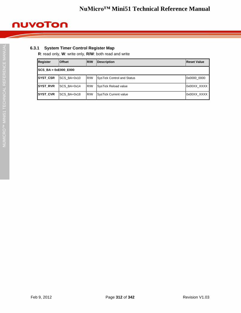
NuMicro™ Mini51 Technical Reference Manual
Feb 9, 2012 Page 312 of 342 Revision V1.03
NU
MIC
RO
™ M
INI5
1 T
EC
HN
ICA
L R
EF
ER
EN
CE
MA
NU
AL
6.3.1 System Timer Control Register Map
R: read only, W: write only, R/W: both read and write
Register Offset R/W Description Reset Value
SCS_BA = 0xE000_E000
SYST_CSR SCS_BA+0x10 R/W SysTick Control and Status 0x0000_0000
SYST_RVR SCS_BA+0x14 R/W SysTick Reload value 0x00XX_XXXX
SYST_CVR SCS_BA+0x18 R/W SysTick Current value 0x00XX_XXXX
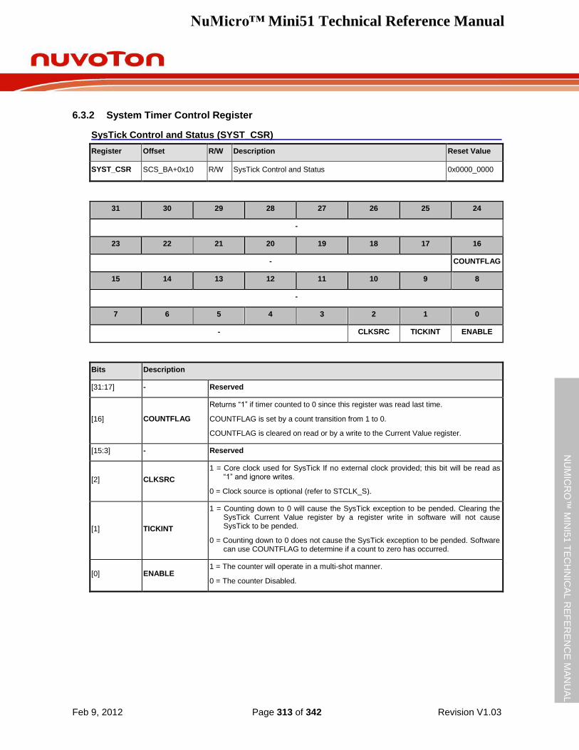
NuMicro™ Mini51 Technical Reference Manual
Feb 9, 2012 Page 313 of 342 Revision V1.03
NU
MIC
RO
™ M
INI5
1 T
EC
HN
ICA
L R
EF
ER
EN
CE
MA
NU
AL
6.3.2 System Timer Control Register
SysTick Control and Status (SYST_CSR)
Register Offset R/W Description Reset Value
SYST_CSR SCS_BA+0x10 R/W SysTick Control and Status 0x0000_0000
31 30 29 28 27 26 25 24
-
23 22 21 20 19 18 17 16
- COUNTFLAG
15 14 13 12 11 10 9 8
-
7 6 5 4 3 2 1 0
- CLKSRC TICKINT ENABLE
Bits Description
[31:17] - Reserved
[16] COUNTFLAG
Returns “1” if timer counted to 0 since this register was read last time.
COUNTFLAG is set by a count transition from 1 to 0.
COUNTFLAG is cleared on read or by a write to the Current Value register.
[15:3] - Reserved
[2] CLKSRC
1 = Core clock used for SysTick If no external clock provided; this bit will be read as “1” and ignore writes.
0 = Clock source is optional (refer to STCLK_S).
[1] TICKINT
1 = Counting down to 0 will cause the SysTick exception to be pended. Clearing the SysTick Current Value register by a register write in software will not cause SysTick to be pended.
0 = Counting down to 0 does not cause the SysTick exception to be pended. Software can use COUNTFLAG to determine if a count to zero has occurred.
[0] ENABLE 1 = The counter will operate in a multi-shot manner.
0 = The counter Disabled.
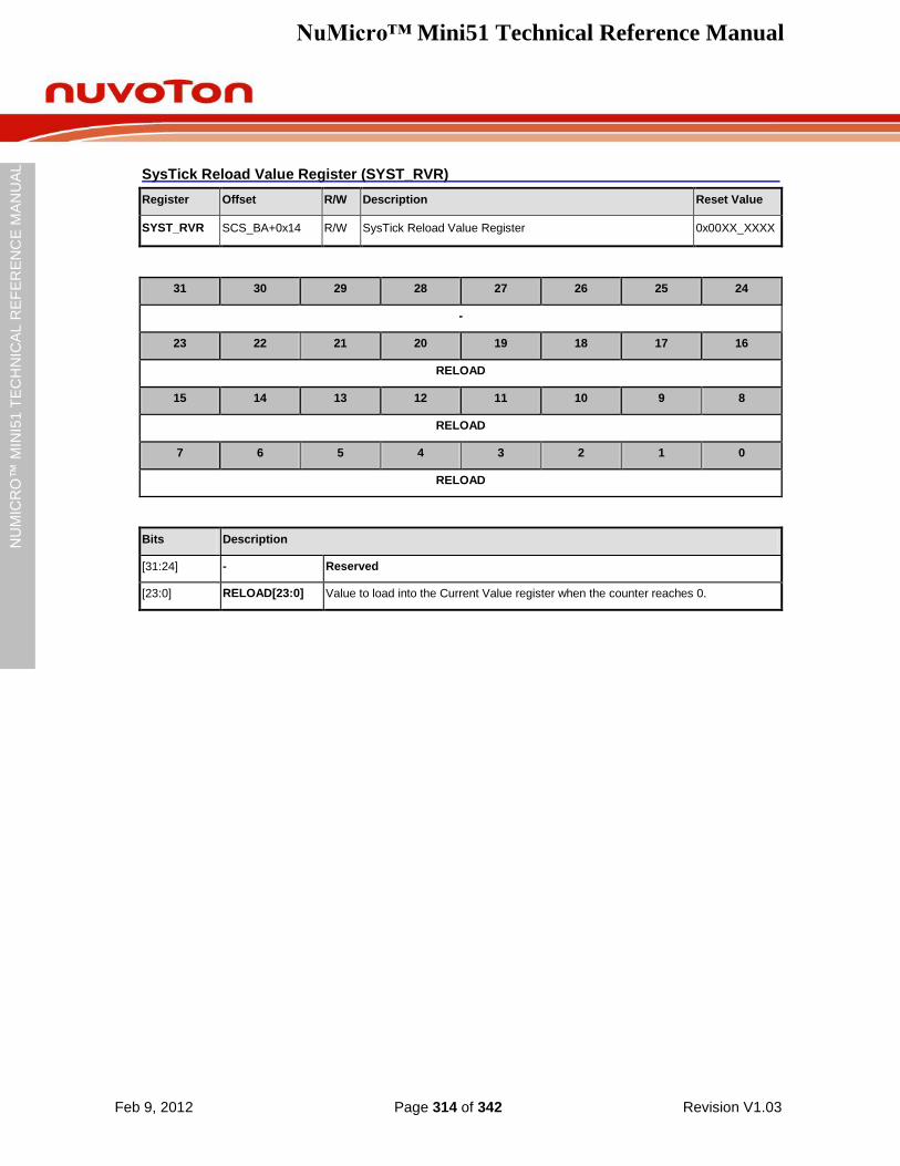
NuMicro™ Mini51 Technical Reference Manual
Feb 9, 2012 Page 314 of 342 Revision V1.03
NU
MIC
RO
™ M
INI5
1 T
EC
HN
ICA
L R
EF
ER
EN
CE
MA
NU
AL
SysTick Reload Value Register (SYST_RVR)
Register Offset R/W Description Reset Value
SYST_RVR SCS_BA+0x14 R/W SysTick Reload Value Register 0x00XX_XXXX
31 30 29 28 27 26 25 24
-
23 22 21 20 19 18 17 16
RELOAD
15 14 13 12 11 10 9 8
RELOAD
7 6 5 4 3 2 1 0
RELOAD
Bits Description
[31:24] - Reserved
[23:0] RELOAD[23:0] Value to load into the Current Value register when the counter reaches 0.
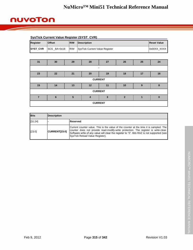
NuMicro™ Mini51 Technical Reference Manual
Feb 9, 2012 Page 315 of 342 Revision V1.03
NU
MIC
RO
™ M
INI5
1 T
EC
HN
ICA
L R
EF
ER
EN
CE
MA
NU
AL
SysTick Current Value Register (SYST_CVR)
Register Offset R/W Description Reset Value
SYST_CVR SCS _BA+0x18 R/W SysTick Current Value Register 0x00XX_XXXX
31 30 29 28 27 26 25 24
-
23 22 21 20 19 18 17 16
CURRENT
15 14 13 12 11 10 9 8
CURRENT
7 6 5 4 3 2 1 0
CURRENT
Bits Description
[31:24] - Reserved
[23:0] CURRENT[23:0]
Current counter value. This is the value of the counter at the time it is sampled. The counter does not provide read-modify-write protection. The register is write-clear. Software write of any value will clear the register to “0”. Bits RAZ is not supported (see SysTick Reload Value Register).
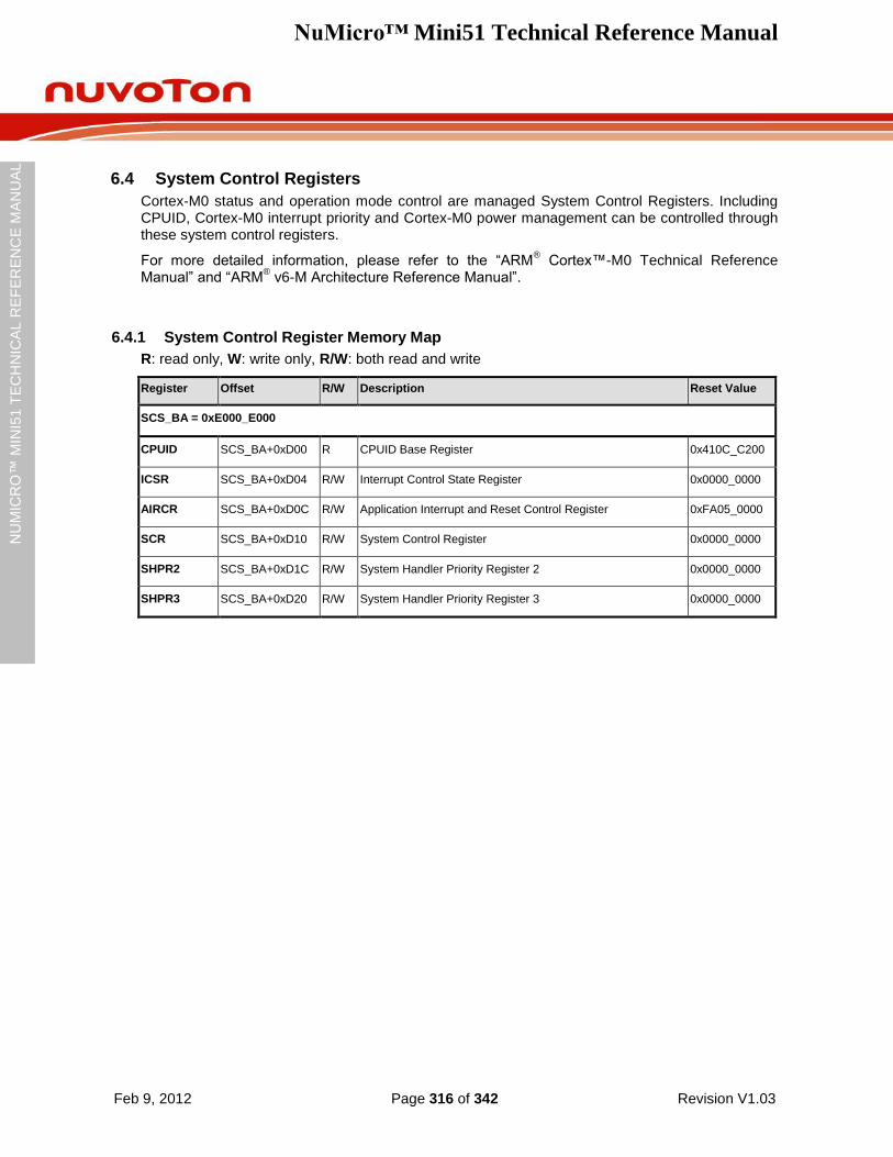
NuMicro™ Mini51 Technical Reference Manual
Feb 9, 2012 Page 316 of 342 Revision V1.03
NU
MIC
RO
™ M
INI5
1 T
EC
HN
ICA
L R
EF
ER
EN
CE
MA
NU
AL
6.4 System Control Registers
Cortex-M0 status and operation mode control are managed System Control Registers. Including CPUID, Cortex-M0 interrupt priority and Cortex-M0 power management can be controlled through these system control registers.
For more detailed information, please refer to the “ARM® Cortex™-M0 Technical Reference
Manual” and “ARM® v6-M Architecture Reference Manual”.
6.4.1 System Control Register Memory Map
R: read only, W: write only, R/W: both read and write
Register Offset R/W Description Reset Value
SCS_BA = 0xE000_E000
CPUID SCS_BA+0xD00 R CPUID Base Register 0x410C_C200
ICSR SCS_BA+0xD04 R/W Interrupt Control State Register 0x0000_0000
AIRCR SCS_BA+0xD0C R/W Application Interrupt and Reset Control Register 0xFA05_0000
SCR SCS_BA+0xD10 R/W System Control Register 0x0000_0000
SHPR2 SCS_BA+0xD1C R/W System Handler Priority Register 2 0x0000_0000
SHPR3 SCS_BA+0xD20 R/W System Handler Priority Register 3 0x0000_0000
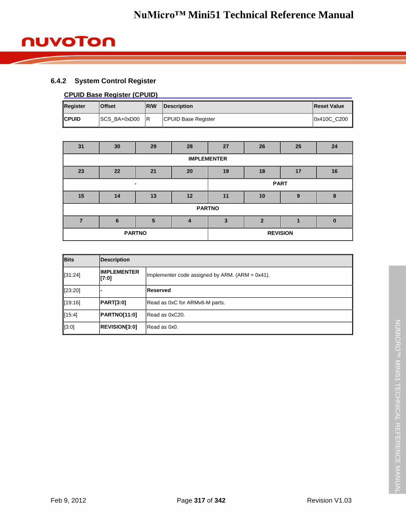
NuMicro™ Mini51 Technical Reference Manual
Feb 9, 2012 Page 317 of 342 Revision V1.03
NU
MIC
RO
™ M
INI5
1 T
EC
HN
ICA
L R
EF
ER
EN
CE
MA
NU
AL
6.4.2 System Control Register
CPUID Base Register (CPUID)
Register Offset R/W Description Reset Value
CPUID SCS_BA+0xD00 R CPUID Base Register 0x410C_C200
31 30 29 28 27 26 25 24
IMPLEMENTER
23 22 21 20 19 18 17 16
- PART
15 14 13 12 11 10 9 8
PARTNO
7 6 5 4 3 2 1 0
PARTNO REVISION
Bits Description
[31:24] IMPLEMENTER [7:0]
Implementer code assigned by ARM. (ARM = 0x41).
[23:20] - Reserved
[19:16] PART[3:0] Read as 0xC for ARMv6-M parts.
[15:4] PARTNO[11:0] Read as 0xC20.
[3:0] REVISION[3:0] Read as 0x0.
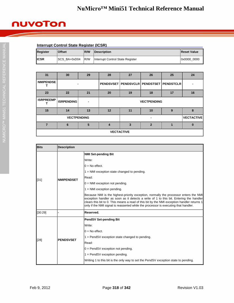
NuMicro™ Mini51 Technical Reference Manual
Feb 9, 2012 Page 318 of 342 Revision V1.03
NU
MIC
RO
™ M
INI5
1 T
EC
HN
ICA
L R
EF
ER
EN
CE
MA
NU
AL
Interrupt Control State Register (ICSR)
Register Offset R/W Description Reset Value
ICSR SCS_BA+0xD04 R/W Interrupt Control State Register 0x0000_0000
31 30 29 28 27 26 25 24
NMIPENDSET
- PENDSVSET PENDSVCLR PENDSTSET PENDSTCLR -
23 22 21 20 19 18 17 16
ISRPREEMPT
ISRPENDING - VECTPENDING
15 14 13 12 11 10 9 8
VECTPENDING - VECTACTIVE
7 6 5 4 3 2 1 0
VECTACTIVE
Bits Description
[31] NMIPENDSET
NMI Set-pending Bit
Write:
0 = No effect.
1 = NMI exception state changed to pending.
Read:
0 = NMI exception not pending.
1 = NMI exception pending.
Because NMI is the highest-priority exception, normally the processor enters the NMI exception handler as soon as it detects a write of 1 to this bit. Entering the handler clears this bit to 0. This means a read of this bit by the NMI exception handler returns 1 only if the NMI signal is reasserted while the processor is executing that handler.
[30:29] - Reserved.
[28] PENDSVSET
PendSV Set-pending Bit
Write:
0 = No effect.
1 = PendSV exception state changed to pending.
Read:
0 = PendSV exception not pending.
1 = PendSV exception pending.
Writing 1 to this bit is the only way to set the PendSV exception state to pending.
NuMicro™ Mini51 Technical Reference Manual
Feb 9, 2012 Page 319 of 342 Revision V1.03
NU
MIC
RO
™ M
INI5
1 T
EC
HN
ICA
L R
EF
ER
EN
CE
MA
NU
AL
Bits Description
[27] PENDSVCLR
PendSV Clear-pending Bit (Write Only)
Write:
0 = No effect.
1 = The pending state removed from the PendSV exception.
[26] PENDSTSET
SysTick Exception Set-pending Bit
Write:
0 = No effect.
1 = SysTick exception state changed to pending.
Read:
0 = SysTick exception not pending.
1 = SysTick exception pending.
[25] PENDSTCLR
SysTick Exception Clear-pending Bit (Write Only)
Write:
0 = No effect.
1 = The pending state removed from the SysTick exception.
[24] - Reserved.
[23] ISRPREEMPT Interrupt Preemption (Read Only)
If set, a pending exception will be serviced on exit from the debug halt state.
[22] ISRPENDING
Interrupt Pending Flag (Read Only)
Excluding NMI and Faults.
0 = Interrupt not pending.
1 = Interrupt pending.
[21] - Reserved.
[20:12] VECTPENDING [8:0]
Vector Pending Indicator (Read Only)
This field indicates the exception number of the highest priority pending enabled exception:
0 = No pending exceptions.
Non-zero = The exception number of the highest priority pending enabled exception.
[11:9] - Reserved.
[8:0] VECTACTIVE [8:0]
Vector Active Indicator (Read Only)
This field contains the active exception number:
0 = Thread mode.
Non-zero = The exception number of the currently active exception.
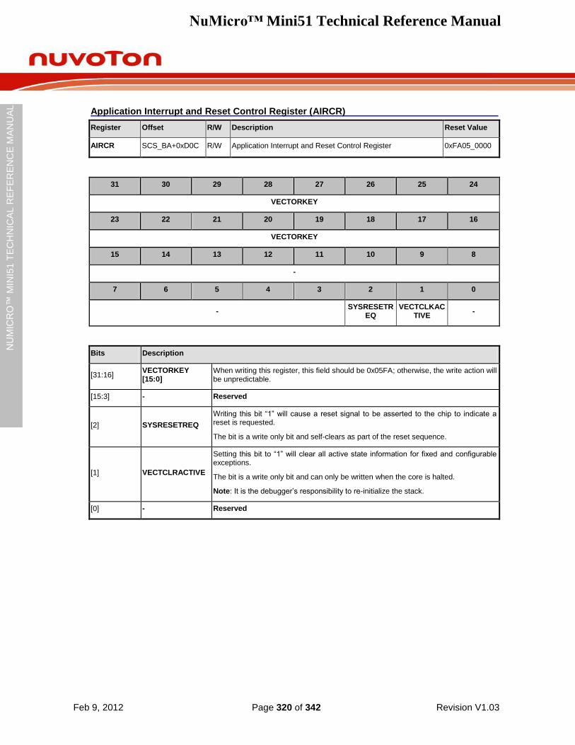
NuMicro™ Mini51 Technical Reference Manual
Feb 9, 2012 Page 320 of 342 Revision V1.03
NU
MIC
RO
™ M
INI5
1 T
EC
HN
ICA
L R
EF
ER
EN
CE
MA
NU
AL
Application Interrupt and Reset Control Register (AIRCR)
Register Offset R/W Description Reset Value
AIRCR SCS_BA+0xD0C R/W Application Interrupt and Reset Control Register 0xFA05_0000
31 30 29 28 27 26 25 24
VECTORKEY
23 22 21 20 19 18 17 16
VECTORKEY
15 14 13 12 11 10 9 8
-
7 6 5 4 3 2 1 0
- SYSRESETR
EQ VECTCLKAC
TIVE -
Bits Description
[31:16] VECTORKEY [15:0]
When writing this register, this field should be 0x05FA; otherwise, the write action will be unpredictable.
[15:3] - Reserved
[2] SYSRESETREQ
Writing this bit “1” will cause a reset signal to be asserted to the chip to indicate a reset is requested.
The bit is a write only bit and self-clears as part of the reset sequence.
[1] VECTCLRACTIVE
Setting this bit to “1” will clear all active state information for fixed and configurable exceptions.
The bit is a write only bit and can only be written when the core is halted.
Note: It is the debugger‟s responsibility to re-initialize the stack.
[0] - Reserved
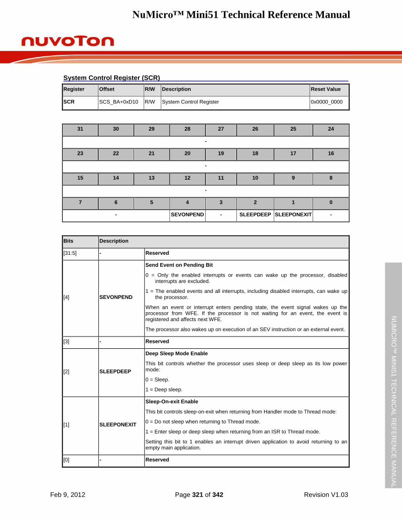
NuMicro™ Mini51 Technical Reference Manual
Feb 9, 2012 Page 321 of 342 Revision V1.03
NU
MIC
RO
™ M
INI5
1 T
EC
HN
ICA
L R
EF
ER
EN
CE
MA
NU
AL
System Control Register (SCR)
Register Offset R/W Description Reset Value
SCR SCS_BA+0xD10 R/W System Control Register 0x0000_0000
31 30 29 28 27 26 25 24
-
23 22 21 20 19 18 17 16
-
15 14 13 12 11 10 9 8
-
7 6 5 4 3 2 1 0
- SEVONPEND - SLEEPDEEP SLEEPONEXIT -
Bits Description
[31:5] - Reserved
[4] SEVONPEND
Send Event on Pending Bit
0 = Only the enabled interrupts or events can wake up the processor, disabled interrupts are excluded.
1 = The enabled events and all interrupts, including disabled interrupts, can wake up the processor.
When an event or interrupt enters pending state, the event signal wakes up the processor from WFE. If the processor is not waiting for an event, the event is registered and affects next WFE.
The processor also wakes up on execution of an SEV instruction or an external event.
[3] - Reserved
[2] SLEEPDEEP
Deep Sleep Mode Enable
This bit controls whether the processor uses sleep or deep sleep as its low power mode:
0 = Sleep.
1 = Deep sleep.
[1] SLEEPONEXIT
Sleep-On-exit Enable
This bit controls sleep-on-exit when returning from Handler mode to Thread mode:
0 = Do not sleep when returning to Thread mode.
1 = Enter sleep or deep sleep when returning from an ISR to Thread mode.
Setting this bit to 1 enables an interrupt driven application to avoid returning to an empty main application.
[0] - Reserved

NuMicro™ Mini51 Technical Reference Manual
Feb 9, 2012 Page 322 of 342 Revision V1.03
NU
MIC
RO
™ M
INI5
1 T
EC
HN
ICA
L R
EF
ER
EN
CE
MA
NU
AL
System Handler Priority Register 2 (SHPR2)
Register Offset R/W Description Reset Value
SHPR2 SCS_BA+0xD1C R/W System Handler Priority Register 2 0x0000_0000
31 30 29 28 27 26 25 24
PRI_11 -
23 22 21 20 19 18 17 16
-
15 14 13 12 11 10 9 8
-
7 6 5 4 3 2 1 0
-
Bits Description
[31:30] PRI_11[1:0] Priority of System Handler 11 – SVCall
“0” denotes the highest priority and “3” denotes the lowest priority.
[29:0] - Reserved
NuMicro™ Mini51 Technical Reference Manual
Feb 9, 2012 Page 323 of 342 Revision V1.03
NU
MIC
RO
™ M
INI5
1 T
EC
HN
ICA
L R
EF
ER
EN
CE
MA
NU
AL
System Handler Priority Register 3 (SHPR3)
Register Offset R/W Description Reset Value
SHPR3 SCS_BA+0xD20 R/W System Handler Priority Register 3 0x0000_0000
31 30 29 28 27 26 25 24
PRI_15 -
23 22 21 20 19 18 17 16
PRI_14 -
15 14 13 12 11 10 9 8
-
7 6 5 4 3 2 1 0
-
Bits Description
[31:30] PRI_15[1:0] Priority of System Handler 15 – SysTick
“0” denotes the highest priority and “3” denotes the lowest priority.
[29:24] - Reserved
[23:22] PRI_14[1:0] Priority of System Handler 14 – PendSV
“0” denotes the highest priority and “3” denotes the lowest priority.
[21:0] - Reserved
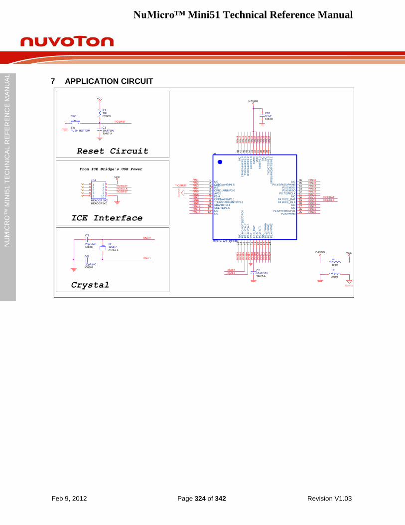
NuMicro™ Mini51 Technical Reference Manual
Feb 9, 2012 Page 324 of 342 Revision V1.03
NU
MIC
RO
™ M
INI5
1 T
EC
HN
ICA
L R
EF
ER
EN
CE
MA
NU
AL
7 APPLICATION CIRCUIT
TICEDAT
PIN3
X212MHzXTAL3-1
PIN
46
PIN30
SW1
PUSH BOTTOMSW
TICERST
PIN
45
PIN27PIN10
C110uF/10VTANT-A
PIN
42
PIN34
PIN
15 VCC
PIN9
U1
MINI54LAN LQFP48
44
45
46
47
48
21
6
17
18
19
20
21
22
23
24
26
2930
3233343536
37
38
39
345
9
78
101112
13
31
28
41
43
42
40
14
16
15
25
27
AIN
1/P
1.0
RX
D/A
IN2/P
1.2
TX
D/A
IN3/P
1.3
CP
N0/A
IN4/P
1.4
NC
CPP0/AIN5/P1.5NC
P5.4
VS
SLD
O_C
AP
P5.5
P5.2
/IN
T1
NC
P2.2
/PW
M0
P2.3
/PW
M1
P2.4
/PW
M2
P2.6/PWM4/CPO1
P4.6/ICE_CLKP4.7/ICE_DAT
P0.7/SPICLKP0.6/MISOP0.5/MOSI
P0.4/SPISS/PWM5NCS
PIS
S/R
XD
/RT
S/P
0.1
TX
D/C
TS
/P0.0
NC
RSTCPN1/AIN6/P3.0AVSS
SDA/T0/P3.4
CPP1/AIN7/P3.1T0EX/STADC/INT0/P3.2
SCL/T1/P3.5NCNC
NC
NC
NC
AIN
0/P
5.3
AV
DD
VD
D
NC
P3.6
/CK
O/T
1E
X/C
PO
0
P5.0
/XT
AL1
P5.1
/XT
AL2
P2.5/PWM3
NC
TICECLK
PIN
40
C210uF/10VTANT-A
PIN
16
PIN
18
TICERST
XTAL2
PIN26
C3
20pF/NCC0603
PIN
19
PIN
39
TICEDAT
PIN
47
ICE Interface
C5
20pF/NCC0603
PIN
20
PIN
37
PIN11
Crystal
DAVDD
PIN25
PIN
38
PIN
23
PIN1
From ICE Bridge's USB Power
PIN28
PIN
48
XTAL2
PIN
24
PIN6
L1
L0603
XTAL1
Reset Circuit
TICECLK
DAVDD
PIN
21
PIN12
JP4
HEADER 5X2HEADER5x2
1 23 45 67 89 10
PIN29
PIN36
PIN4
PIN
13
PIN31
R110KR0603
PIN35
PIN7
PIN
44
PIN
17
PIN32
ADAVSS
XTAL1
PIN8
ADAVSS
PIN
41
VCC
PIN
22
PIN33
CB10.1uFC0603
PIN2
TICERST
VCC
PIN
14
PIN5
PIN
43
L2
L0603
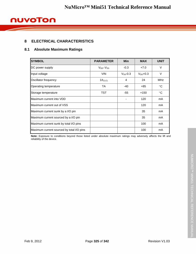
NuMicro™ Mini51 Technical Reference Manual
Feb 9, 2012 Page 325 of 342 Revision V1.03
NU
MIC
RO
™ M
INI5
1 T
EC
HN
ICA
L R
EF
ER
EN
CE
MA
NU
AL
8 ELECTRICAL CHARACTERISTICS
8.1 Absolute Maximum Ratings
SYMBOL PARAMETER Min MAX UNIT
DC power supply VDDVSS -0.3 +7.0 V
Input voltage VIN VSS-0.3 VDD+0.3 V
Oscillator frequency 1/tCLCL 4 24 MHz
Operating temperature TA -40 +85 C
Storage temperature TST -55 +150 C
Maximum current into VDD - 120 mA
Maximum current out of VSS 120 mA
Maximum current sunk by a I/O pin 35 mA
Maximum current sourced by a I/O pin 35 mA
Maximum current sunk by total I/O pins 100 mA
Maximum current sourced by total I/O pins 100 mA
Note: Exposure to conditions beyond those listed under absolute maximum ratings may adversely affects the lift and reliability of the device.
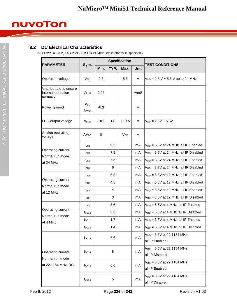
NuMicro™ Mini51 Technical Reference Manual
Feb 9, 2012 Page 326 of 342 Revision V1.03
NU
MIC
RO
™ M
INI5
1 T
EC
HN
ICA
L R
EF
ER
EN
CE
MA
NU
AL
8.2 DC Electrical Characteristics
(VDD-VSS = 5.0 V, TA = 25C, FOSC = 24 MHz unless otherwise specified.)
PARAMETER Sym. Specification
TEST CONDITIONS Min. TYP. Max. Unit
Operation voltage VDD 2.5 5.5 V VDD = 2.5 V ~ 5.5 V up to 24 MHz
VDD rise rate to ensure internal operation correctly
VRISE 0.05 V/mS
Power ground VSS
AVSS -0.3 V
LDO output voltage VLDO -10% 1.8 +10% V VDD = 2.5V ~ 5.5V
Analog operating voltage
AVDD 0 VDD V
Operating current
Normal run mode
at 24 MHz
IDD1 9.5 mA VDD = 5.5V at 24 MHz, all IP Enabled
IDD2 7.5 mA VDD = 5.5V at 24 MHz, all IP Disabled
IDD3 7.5 mA VDD = 3.3V at 24 MHz, all IP Enabled
IDD4 6 mA VDD = 3.3V at 24 MHz, all IP Disabled
Operating current
Normal run mode
at 12 MHz
IDD5 5.5 mA VDD = 5.5V at 12 MHz, all IP Enabled
IDD6 4.5 mA VDD = 5.5V at 12 MHz, all IP Disabled
IDD7 4 mA VDD = 3.3V at 12 MHz, all IP Enabled
IDD8 3 mA VDD = 3.3V at 12 MHz, all IP Disabled
Operating current
Normal run mode
at 4 MHz
IDD9 3.6 mA VDD = 5.5V at 4 MHz, all IP Enabled
IDD10 3.3 mA VDD = 5.5V at 4 MHz, all IP Disabled
IDD11 1.7 mA VDD = 3.3V at 4 MHz, all IP Enabled
IDD12 1.4 mA VDD = 3.3V at 4 MHz, all IP Disabled
Operating current
Normal run mode
at 22.1184 MHz IRC
IDD13
6.6 mA VDD = 5.5V at 22.1184 MHz,
all IP Enabled
IDD14
5 mA VDD = 5.5V at 22.1184 MHz,
all IP Disabled
IDD15
6.6 mA VDD = 3.3V at 22.1184 MHz,
all IP Enabled
IDD16
5 mA VDD = 3.3V at 22.1184 MHz,
all IP Disabled
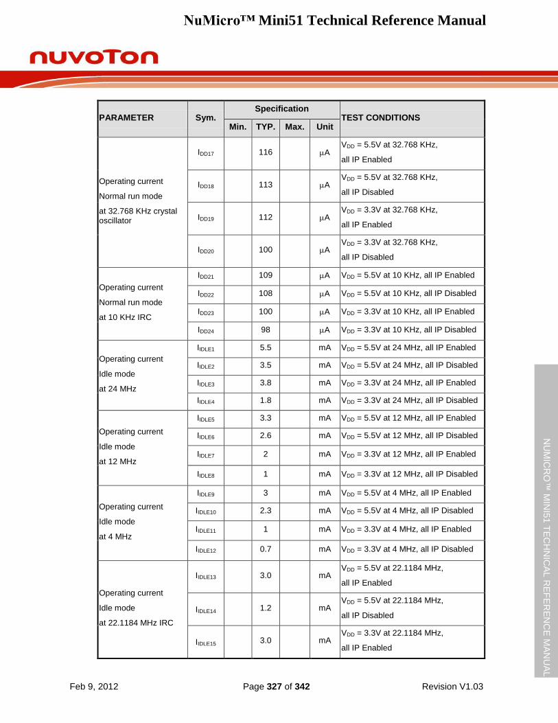
NuMicro™ Mini51 Technical Reference Manual
Feb 9, 2012 Page 327 of 342 Revision V1.03
NU
MIC
RO
™ M
INI5
1 T
EC
HN
ICA
L R
EF
ER
EN
CE
MA
NU
AL
PARAMETER Sym. Specification
TEST CONDITIONS Min. TYP. Max. Unit
Operating current
Normal run mode
at 32.768 KHz crystal oscillator
IDD17 116 A VDD = 5.5V at 32.768 KHz,
all IP Enabled
IDD18 113 A VDD = 5.5V at 32.768 KHz,
all IP Disabled
IDD19 112 A VDD = 3.3V at 32.768 KHz,
all IP Enabled
IDD20 100 A VDD = 3.3V at 32.768 KHz,
all IP Disabled
Operating current
Normal run mode
at 10 KHz IRC
IDD21 109 A VDD = 5.5V at 10 KHz, all IP Enabled
IDD22 108 A VDD = 5.5V at 10 KHz, all IP Disabled
IDD23 100 A VDD = 3.3V at 10 KHz, all IP Enabled
IDD24 98 A VDD = 3.3V at 10 KHz, all IP Disabled
Operating current
Idle mode
at 24 MHz
IIDLE1 5.5 mA VDD = 5.5V at 24 MHz, all IP Enabled
IIDLE2 3.5 mA VDD = 5.5V at 24 MHz, all IP Disabled
IIDLE3 3.8 mA VDD = 3.3V at 24 MHz, all IP Enabled
IIDLE4 1.8 mA VDD = 3.3V at 24 MHz, all IP Disabled
Operating current
Idle mode
at 12 MHz
IIDLE5 3.3 mA VDD = 5.5V at 12 MHz, all IP Enabled
IIDLE6 2.6 mA VDD = 5.5V at 12 MHz, all IP Disabled
IIDLE7 2 mA VDD = 3.3V at 12 MHz, all IP Enabled
IIDLE8 1 mA VDD = 3.3V at 12 MHz, all IP Disabled
Operating current
Idle mode
at 4 MHz
IIDLE9 3 mA VDD = 5.5V at 4 MHz, all IP Enabled
IIDLE10 2.3 mA VDD = 5.5V at 4 MHz, all IP Disabled
IIDLE11 1 mA VDD = 3.3V at 4 MHz, all IP Enabled
IIDLE12 0.7 mA VDD = 3.3V at 4 MHz, all IP Disabled
Operating current
Idle mode
at 22.1184 MHz IRC
IIDLE13 3.0 mA VDD = 5.5V at 22.1184 MHz,
all IP Enabled
IIDLE14 1.2 mA VDD = 5.5V at 22.1184 MHz,
all IP Disabled
IIDLE15 3.0 mA VDD = 3.3V at 22.1184 MHz,
all IP Enabled
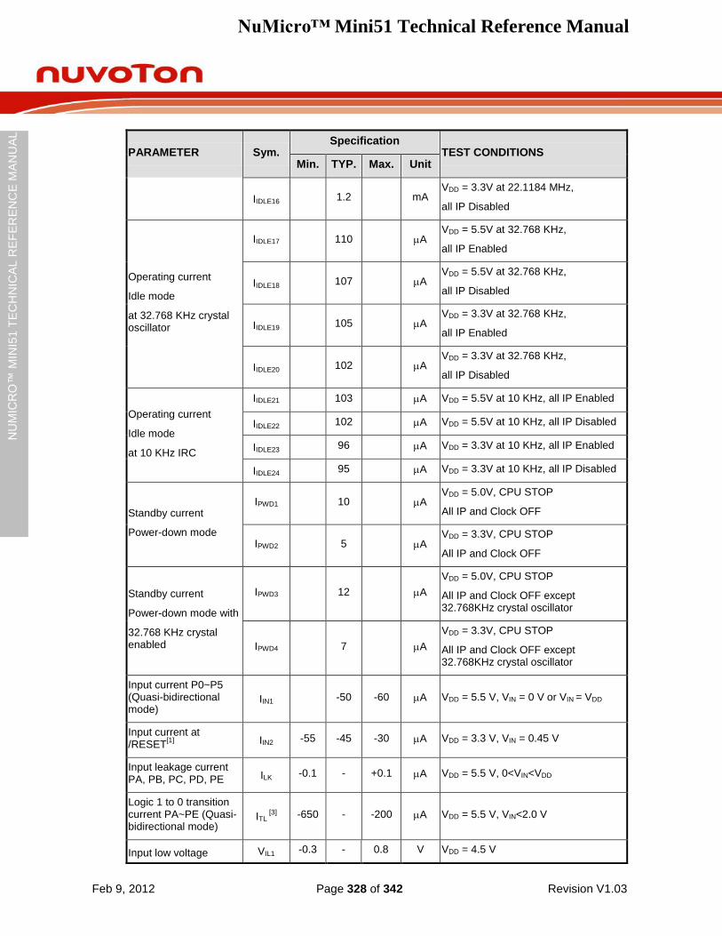
NuMicro™ Mini51 Technical Reference Manual
Feb 9, 2012 Page 328 of 342 Revision V1.03
NU
MIC
RO
™ M
INI5
1 T
EC
HN
ICA
L R
EF
ER
EN
CE
MA
NU
AL
PARAMETER Sym. Specification
TEST CONDITIONS Min. TYP. Max. Unit
IIDLE16 1.2 mA VDD = 3.3V at 22.1184 MHz,
all IP Disabled
Operating current
Idle mode
at 32.768 KHz crystal oscillator
IIDLE17 110 A VDD = 5.5V at 32.768 KHz,
all IP Enabled
IIDLE18 107 A VDD = 5.5V at 32.768 KHz,
all IP Disabled
IIDLE19 105 A VDD = 3.3V at 32.768 KHz,
all IP Enabled
IIDLE20 102 A VDD = 3.3V at 32.768 KHz,
all IP Disabled
Operating current
Idle mode
at 10 KHz IRC
IIDLE21 103 A VDD = 5.5V at 10 KHz, all IP Enabled
IIDLE22 102 A VDD = 5.5V at 10 KHz, all IP Disabled
IIDLE23 96 A VDD = 3.3V at 10 KHz, all IP Enabled
IIDLE24 95 A VDD = 3.3V at 10 KHz, all IP Disabled
Standby current
Power-down mode
IPWD1 10 A VDD = 5.0V, CPU STOP
All IP and Clock OFF
IPWD2 5 A VDD = 3.3V, CPU STOP
All IP and Clock OFF
Standby current
Power-down mode with
32.768 KHz crystal enabled
IPWD3 12 A
VDD = 5.0V, CPU STOP
All IP and Clock OFF except 32.768KHz crystal oscillator
IPWD4 7 A
VDD = 3.3V, CPU STOP
All IP and Clock OFF except 32.768KHz crystal oscillator
Input current P0~P5 (Quasi-bidirectional mode)
IIN1 -50 -60 A VDD = 5.5 V, VIN = 0 V or VIN = VDD
Input current at /RESET
[1] IIN2 -55 -45 -30 A VDD = 3.3 V, VIN = 0.45 V
Input leakage current PA, PB, PC, PD, PE ILK -0.1 - +0.1 A VDD = 5.5 V, 0<VIN<VDD
Logic 1 to 0 transition current PA~PE (Quasi-bidirectional mode)
ITL [3]
-650 - -200 A VDD = 5.5 V, VIN<2.0 V
Input low voltage VIL1 -0.3 - 0.8 V VDD = 4.5 V
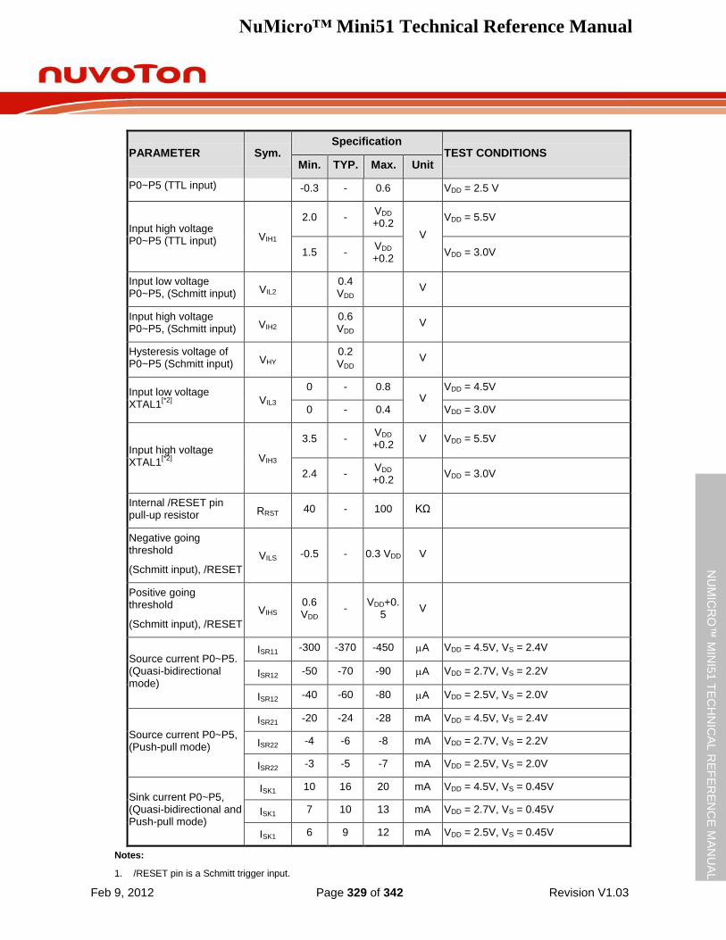
NuMicro™ Mini51 Technical Reference Manual
Feb 9, 2012 Page 329 of 342 Revision V1.03
NU
MIC
RO
™ M
INI5
1 T
EC
HN
ICA
L R
EF
ER
EN
CE
MA
NU
AL
PARAMETER Sym. Specification
TEST CONDITIONS Min. TYP. Max. Unit
P0~P5 (TTL input) -0.3 - 0.6 VDD = 2.5 V
Input high voltage P0~P5 (TTL input) VIH1
2.0 - VDD +0.2
V
VDD = 5.5V
1.5 - VDD +0.2
VDD = 3.0V
Input low voltage P0~P5, (Schmitt input) VIL2
0.4 VDD
V
Input high voltage P0~P5, (Schmitt input) VIH2
0.6 VDD
V
Hysteresis voltage of P0~P5 (Schmitt input) VHY
0.2 VDD
V
Input low voltage XTAL1
[*2] VIL3
0 - 0.8 V
VDD = 4.5V
0 - 0.4 VDD = 3.0V
Input high voltage XTAL1
[*2] VIH3
3.5 - VDD +0.2
V VDD = 5.5V
2.4 - VDD +0.2
VDD = 3.0V
Internal /RESET pin pull-up resistor RRST 40 - 100 KΩ
Negative going threshold
(Schmitt input), /RESET
VILS -0.5 - 0.3 VDD V
Positive going threshold
(Schmitt input), /RESET
VIHS 0.6 VDD
- VDD+0.
5 V
Source current P0~P5. (Quasi-bidirectional mode)
ISR11 -300 -370 -450 A VDD = 4.5V, VS = 2.4V
ISR12 -50 -70 -90 A VDD = 2.7V, VS = 2.2V
ISR12 -40 -60 -80 A VDD = 2.5V, VS = 2.0V
Source current P0~P5, (Push-pull mode)
ISR21 -20 -24 -28 mA VDD = 4.5V, VS = 2.4V
ISR22 -4 -6 -8 mA VDD = 2.7V, VS = 2.2V
ISR22 -3 -5 -7 mA VDD = 2.5V, VS = 2.0V
Sink current P0~P5, (Quasi-bidirectional and Push-pull mode)
ISK1 10 16 20 mA VDD = 4.5V, VS = 0.45V
ISK1 7 10 13 mA VDD = 2.7V, VS = 0.45V
ISK1 6 9 12 mA VDD = 2.5V, VS = 0.45V
Notes:
1. /RESET pin is a Schmitt trigger input.

NuMicro™ Mini51 Technical Reference Manual
Feb 9, 2012 Page 330 of 342 Revision V1.03
NU
MIC
RO
™ M
INI5
1 T
EC
HN
ICA
L R
EF
ER
EN
CE
MA
NU
AL
2. Crystal Input is a CMOS input.
3. Pins of P0~P5 can source a transition current when they are being externally driven from 1 to 0. In the condition of VDD=5.5V, the transition current reaches its maximum value when VIN approximates to 2V.
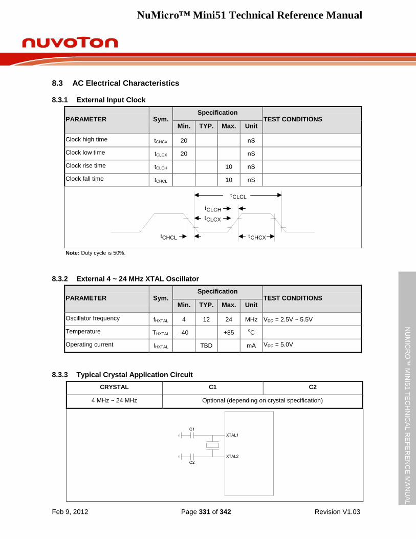
NuMicro™ Mini51 Technical Reference Manual
Feb 9, 2012 Page 331 of 342 Revision V1.03
NU
MIC
RO
™ M
INI5
1 T
EC
HN
ICA
L R
EF
ER
EN
CE
MA
NU
AL
8.3 AC Electrical Characteristics
8.3.1 External Input Clock
PARAMETER Sym. Specification
TEST CONDITIONS Min. TYP. Max. Unit
Clock high time tCHCX 20 nS
Clock low time tCLCX 20 nS
Clock rise time tCLCH 10 nS
Clock fall time tCHCL 10 nS
tCLCL
tCLCX
tCHCX
tCLCH
tCHCL
Note: Duty cycle is 50%.
8.3.2 External 4 ~ 24 MHz XTAL Oscillator
PARAMETER Sym. Specification
TEST CONDITIONS Min. TYP. Max. Unit
Oscillator frequency fHXTAL 4 12 24 MHz VDD = 2.5V ~ 5.5V
Temperature THXTAL -40 +85 oC
Operating current IHXTAL TBD mA VDD = 5.0V
8.3.3 Typical Crystal Application Circuit
CRYSTAL C1 C2
4 MHz ~ 24 MHz Optional (depending on crystal specification)
XTAL2
XTAL1
C1
C2
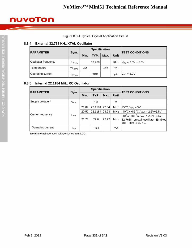
NuMicro™ Mini51 Technical Reference Manual
Feb 9, 2012 Page 332 of 342 Revision V1.03
NU
MIC
RO
™ M
INI5
1 T
EC
HN
ICA
L R
EF
ER
EN
CE
MA
NU
AL
Figure 8.3-1 Typical Crystal Application Circuit
8.3.4 External 32.768 KHz XTAL Oscillator
PARAMETER Sym. Specification
TEST CONDITIONS Min. TYP. Max. Unit
Oscillator frequency fLXTAL 32.768 KHz VDD = 2.5V ~ 5.5V
Temperature TLXTAL -40 +85 oC
Operating current IHXTAL TBD A VDD = 5.0V
8.3.5 Internal 22.1184 MHz RC Oscillator
PARAMETER Sym. Specification
TEST CONDITIONS Min. TYP. Max. Unit
Supply voltage[1]
VHRC 1.8 V
Center frequency FHRC
21.89 22.1184 22.34 MHz 25oC, VDD = 5V
20.57 22.1184 23.23 MHz -40oC~+85
oC, VDD = 2.5V~5.5V
21.78 22.0 22.22 MHz
-40oC~+85
oC, VDD = 2.5V~5.5V
32.768K crystal oscillator Enabled and TRIM_SEL = 1
Operating current IHRC TBD mA
Note: Internal operation voltage comes from LDO.
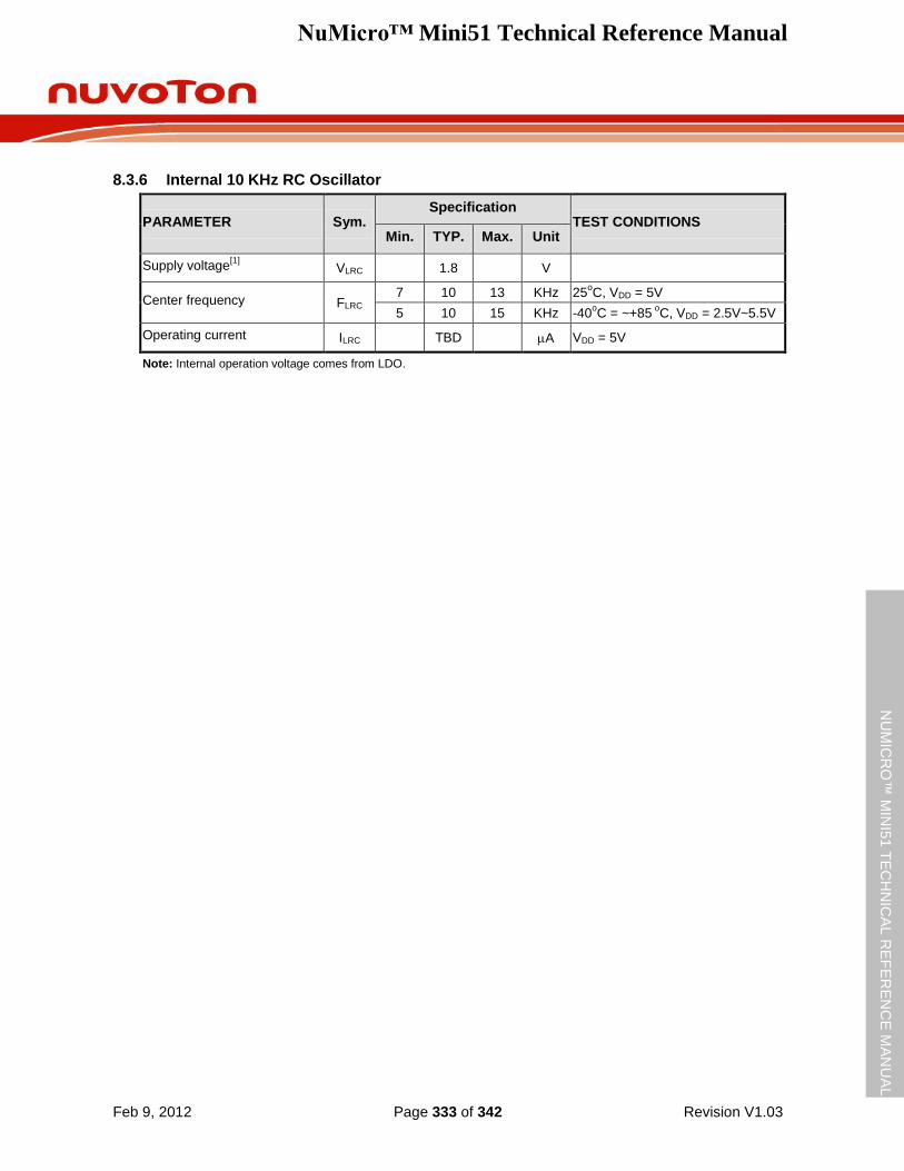
NuMicro™ Mini51 Technical Reference Manual
Feb 9, 2012 Page 333 of 342 Revision V1.03
NU
MIC
RO
™ M
INI5
1 T
EC
HN
ICA
L R
EF
ER
EN
CE
MA
NU
AL
8.3.6 Internal 10 KHz RC Oscillator
PARAMETER Sym. Specification
TEST CONDITIONS Min. TYP. Max. Unit
Supply voltage[1]
VLRC 1.8 V
Center frequency FLRC 7 10 13 KHz 25
oC, VDD = 5V
5 10 15 KHz -40oC = ~+85
oC, VDD = 2.5V~5.5V
Operating current ILRC TBD A VDD = 5V
Note: Internal operation voltage comes from LDO.
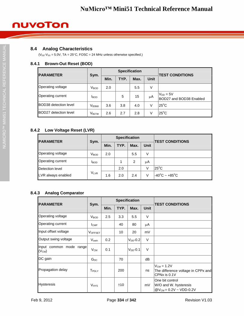
NuMicro™ Mini51 Technical Reference Manual
Feb 9, 2012 Page 334 of 342 Revision V1.03
NU
MIC
RO
™ M
INI5
1 T
EC
HN
ICA
L R
EF
ER
EN
CE
MA
NU
AL
8.4 Analog Characteristics
(VDD-VSS = 5.0V, TA = 25C, FOSC = 24 MHz unless otherwise specified.)
8.4.1 Brown-Out Reset (BOD)
PARAMETER Sym. Specification
TEST CONDITIONS Min. TYP. Max. Unit
Operating voltage VBOD 2.0 5.5 V
Operating current IBOD 5 15 A VDD = 5V
BOD27 and BOD38 Enabled
BOD38 detection level VB38dt 3.6 3.8 4.0 V 25oC
BOD27 detection level VB27dt 2.6 2.7 2.8 V 25oC
8.4.2 Low Voltage Reset (LVR)
PARAMETER Sym. Specification
TEST CONDITIONS Min. TYP. Max. Unit
Operating voltage VBOD 2.0 5.5 V
Operating current IBOD 1 2 A
Detection level
LVR always enabled VLVR
2.0 V 25oC
1.6 2.0 2.4 V -40oC ~ +85
oC
8.4.3 Analog Comparator
PARAMETER Sym. Specification
TEST CONDITIONS Min. TYP. Max. Unit
Operating voltage VBOD 2.5 3.3 5.5 V
Operating current ICMP 40 80 A
Input offset voltage VOFFSET 10 20 mV
Output swing voltage Vswin 0.2 VDD-0.2 V
Input common mode range (VCM) VCM 0.1 VDD-0.1 V
DC gain GDC 70 dB
Propagation delay TPDLY 200 ns
VCM = 1.2V
The difference voltage in CPPx and CPNx is 0.1V
Hysteresis VHYS ±10 mV
One bit control
W/O and W. hysteresis
@VCM = 0.2V ~ VDD-0.2V
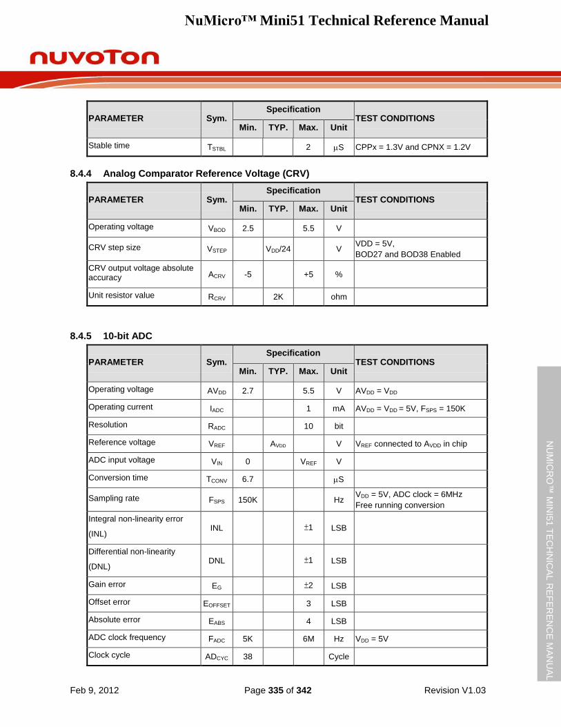
NuMicro™ Mini51 Technical Reference Manual
Feb 9, 2012 Page 335 of 342 Revision V1.03
NU
MIC
RO
™ M
INI5
1 T
EC
HN
ICA
L R
EF
ER
EN
CE
MA
NU
AL
PARAMETER Sym. Specification
TEST CONDITIONS Min. TYP. Max. Unit
Stable time TSTBL 2 S CPPx = 1.3V and CPNX = 1.2V
8.4.4 Analog Comparator Reference Voltage (CRV)
PARAMETER Sym. Specification
TEST CONDITIONS Min. TYP. Max. Unit
Operating voltage VBOD 2.5 5.5 V
CRV step size VSTEP VDD/24 V VDD = 5V,
BOD27 and BOD38 Enabled
CRV output voltage absolute accuracy ACRV -5 +5 %
Unit resistor value RCRV 2K ohm
8.4.5 10-bit ADC
PARAMETER Sym. Specification
TEST CONDITIONS Min. TYP. Max. Unit
Operating voltage AVDD 2.7 5.5 V AVDD = VDD
Operating current IADC 1 mA AVDD = VDD = 5V, FSPS = 150K
Resolution RADC 10 bit
Reference voltage VREF AVDD V VREF connected to AVDD in chip
ADC input voltage VIN 0 VREF V
Conversion time TCONV 6.7 S
Sampling rate FSPS 150K Hz VDD = 5V, ADC clock = 6MHz
Free running conversion
Integral non-linearity error
(INL) INL ±1 LSB
Differential non-linearity
(DNL) DNL ±1 LSB
Gain error EG ±2 LSB
Offset error EOFFSET 3 LSB
Absolute error EABS 4 LSB
ADC clock frequency FADC 5K 6M Hz VDD = 5V
Clock cycle ADCYC 38 Cycle
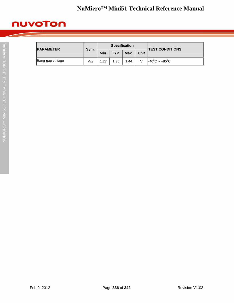
NuMicro™ Mini51 Technical Reference Manual
Feb 9, 2012 Page 336 of 342 Revision V1.03
NU
MIC
RO
™ M
INI5
1 T
EC
HN
ICA
L R
EF
ER
EN
CE
MA
NU
AL
PARAMETER Sym. Specification
TEST CONDITIONS Min. TYP. Max. Unit
Bang-gap voltage VBG 1.27 1.35 1.44 V -40oC ~ +85
oC
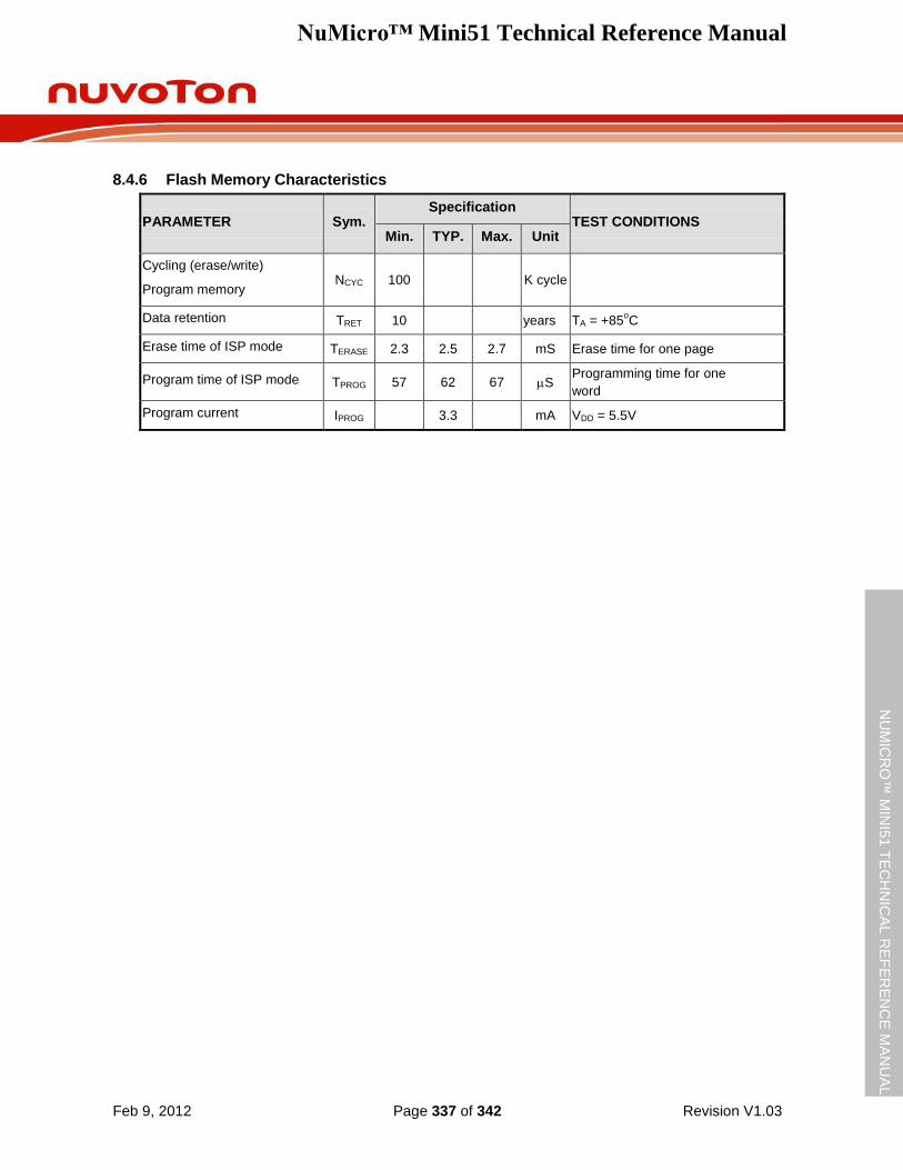
NuMicro™ Mini51 Technical Reference Manual
Feb 9, 2012 Page 337 of 342 Revision V1.03
NU
MIC
RO
™ M
INI5
1 T
EC
HN
ICA
L R
EF
ER
EN
CE
MA
NU
AL
8.4.6 Flash Memory Characteristics
PARAMETER Sym. Specification
TEST CONDITIONS Min. TYP. Max. Unit
Cycling (erase/write)
Program memory NCYC 100 K cycle
Data retention TRET 10 years TA = +85oC
Erase time of ISP mode TERASE 2.3 2.5 2.7 mS Erase time for one page
Program time of ISP mode TPROG 57 62 67 S Programming time for one
word
Program current IPROG 3.3 mA VDD = 5.5V
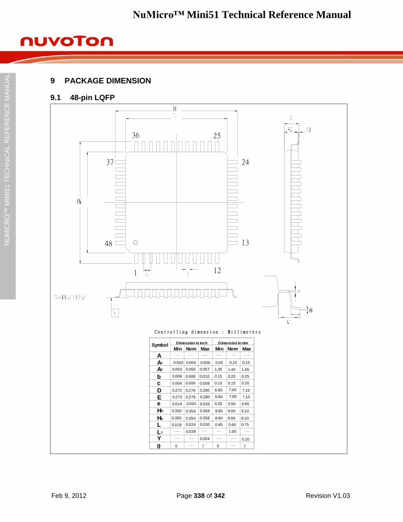
NuMicro™ Mini51 Technical Reference Manual
Feb 9, 2012 Page 338 of 342 Revision V1.03
NU
MIC
RO
™ M
INI5
1 T
EC
HN
ICA
L R
EF
ER
EN
CE
MA
NU
AL
9 PACKAGE DIMENSION
9.1 48-pin LQFP
1 12
48
H
H
C o n t r o l l i n g d i me n s i o n : M i l l i m e t e r s
0.10
070
0.004
1.00
0.750.600.45
0.039
0.0300.0240.018
9.109.008.900.3580.3540.350
0.50
0.20
0.25
1.451.40
0.10
0.15
1.35
0.008
0.010
0.0570.055
0.026
7.107.006.900.2800.2760.272
0.004
0.006
0.053
SymbolMin Nom Max MaxNomMin
Dimension in inch Dimension in mm
A
bc
D
e
HD
HE
L
Y
0
AA
L1
1
2
E
0.008
0.006 0.15
0.20
7
0.020 0.35 0.65
0.100.050.002 0.004 0.006 0.15
9.109.008.900.3580.3540.350
7.107.006.900.2800.2760.272
0.014
37
36 25
24
13
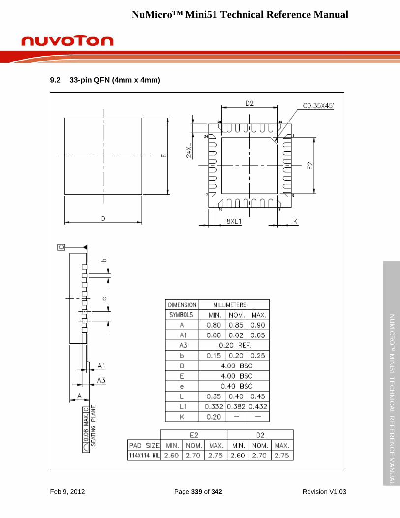
NuMicro™ Mini51 Technical Reference Manual
Feb 9, 2012 Page 339 of 342 Revision V1.03
NU
MIC
RO
™ M
INI5
1 T
EC
HN
ICA
L R
EF
ER
EN
CE
MA
NU
AL
9.2 33-pin QFN (4mm x 4mm)
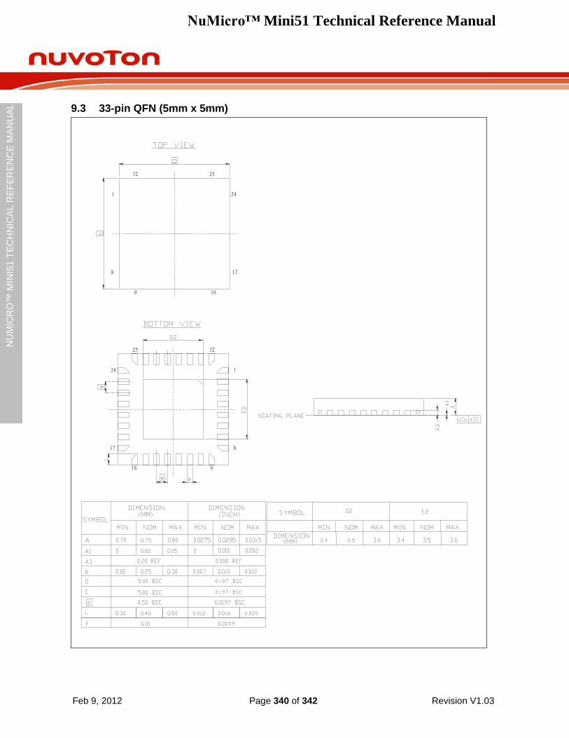
NuMicro™ Mini51 Technical Reference Manual
Feb 9, 2012 Page 340 of 342 Revision V1.03
NU
MIC
RO
™ M
INI5
1 T
EC
HN
ICA
L R
EF
ER
EN
CE
MA
NU
AL
9.3 33-pin QFN (5mm x 5mm)
1
8
8
9 16
1
16
17
17
9
24
24
32 25
25 32
NuMicro™ Mini51 Technical Reference Manual
Feb 9, 2012 Page 341 of 342 Revision V1.03
NU
MIC
RO
™ M
INI5
1 T
EC
HN
ICA
L R
EF
ER
EN
CE
MA
NU
AL
10 REVISION HISTORY
Date Revision Changes
Sep 6, 2011 1.00 Initial release
Oct 20, 2011 1.01
1. Changed electrical characteristics of comparator, 22 MHz RC oscillator, ADC and band-gap.
2. Added electrical characteristics of Flash memory.
3. Changed maximum SPI frequency as 12MHz.
4. Added more description about ADC channel enable register (ADCHER).
5. Modified the block diagram of timer controller.
6. Modified the description of timer capture mode.
7. Fixed some typos.
Dec 1, 2011 1.02
1. Fixed electrical characteristics of 22 MHz RC oscillator.
2. Modified all “1XX” description in registers and related figures.
3. Updated “Figure 5.10-18: Motor Control PWM Architecture”.
4. Updated “Figure 5.10-17: Initial State and Polarity Control with Rising Edge Dead-zone Insertion”.
5. Revised the TIF (bit 0 TISR register) description.
6. Changed the SYST_CSR reset value from “0x0000_0004” to “0x0000_0000”.
7. Modified 33-pin QFN 5mm x 5mm package outline specification.
8. Fixed some typos.
Feb 9, 2012 1.03
1. Added the VDD rise rate specification.
2. Revised the minimum ADC clock frequency specification.
3. Revised the minimum and maximum specification of band-gap voltage.
4. Added a note about only even channels (PWM0, PWM2 and PWM4) can be set as inverter bit (CHnINV, n = 0, 2, 4) in independent mode.
5. Modified the diagram in the LEV_RTS (bit 9 of UA_MCR register) description.
6. Added the CFGUEN and LDUEN bit description in the ISP Control Register (ISPCON) section.
NuMicro™ Mini51 Technical Reference Manual
Feb 9, 2012 Page 342 of 342 Revision V1.03
NU
MIC
RO
™ M
INI5
1 T
EC
HN
ICA
L R
EF
ER
EN
CE
MA
NU
AL
Important Notice
Nuvoton Products are neither intended nor warranted for usage in systems or equipment, any malfunction or failure of which may cause loss of human life, bodily injury or severe property damage. Such applications are deemed, “Insecure Usage”.
Insecure usage includes, but is not limited to: equipment for surgical implementation, atomic energy control instruments, airplane or spaceship instruments, the control or operation of dynamic, brake or safety systems designed for vehicular use, traffic signal instruments, all types of safety devices, and other applications intended to support or sustain life.
All Insecure Usage shall be made at customer’s risk, and in the event that third parties lay claims to Nuvoton as a result of customer’s Insecure Usage, customer shall indemnify the damages and liabilities thus incurred by Nuvoton.