Embed Size (px)
Citation preview

Numerical Simulation of a Dipole Antenna Coupling to a Thin Wire in the Near Field
Yaping Zhang, John Paul, C Christopoulos
George Green Institute for Electromagnetics Research
University of Nottingham, Nottingham NG7 2RD, UK
www.nottingham.ac.uk/ggiemr/
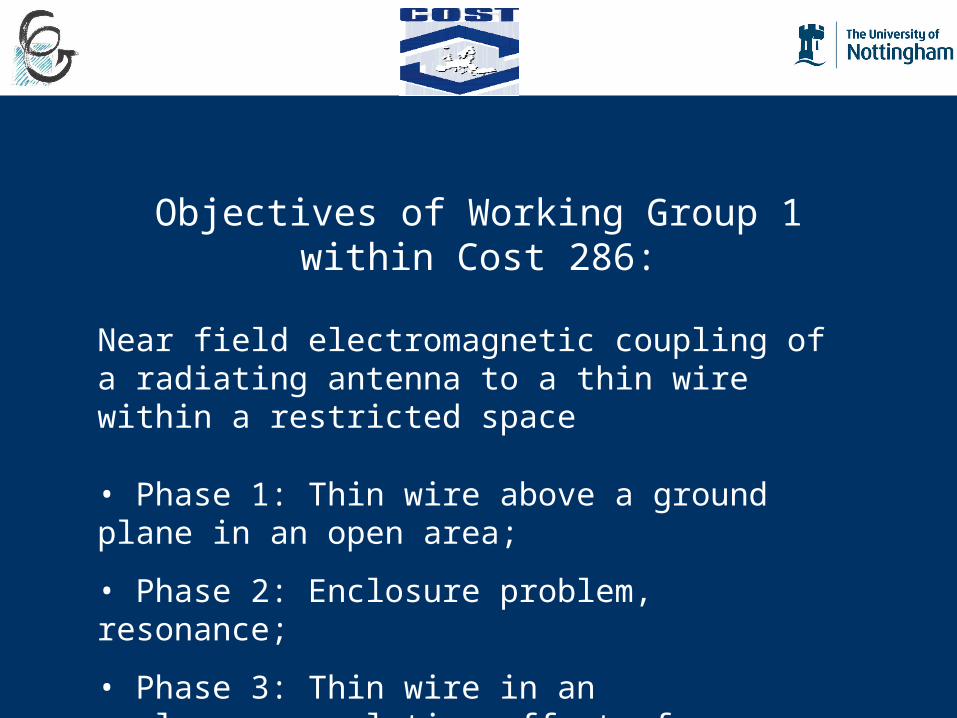
Objectives of Working Group 1 within Cost 286:
Near field electromagnetic coupling of a radiating antenna to a thin wire within a restricted space
• Phase 1: Thin wire above a ground plane in an open area;
• Phase 2: Enclosure problem, resonance;
• Phase 3: Thin wire in an enclosure,cumulative effect of
more sources.

Configurations of the Simulation Models
Phase 1: Thin wire above a ground plane in an open area
Two configurations are simulated using the Transmission Line Modelling (TLM) method. The dipole antenna is parallel or perpendicular to the thin wire, as shown in Fig.1 (a)-(b).
3 m
half wave dipole antenna
1.5 m
h1=0.1 mh2=0.3 m
aligned
1m
V
100
V
100
50
6 m 6 m
half wave dipole antenna
1.5 m
h1=0.1 mh2=0.3 m
0.3m
1m
VV
100
50
0
y
xz
3 m
(a) (b)
Fig.1 Configurations of the simulation models:
(a) a dipole antenna parallel to a thin wire above a ground plane;
(b) a dipole antenna perpendicular to a thin wire above a ground plane.

The problem is considered taking into account the final configuration that needs to be tackled namely the case of coupling inside an imperfect cavity (vehicle with windows, non-metallic walls) and in the presence of people (very complex EM properties).
Under these circumstances the advantages of MoM models in describing wires are no longer decisive and differential time-domain models such as TLM and FDTD appear to be advantageous!
However, special techniques are required to describe thin wires (electrically small dimensions) inside cabinets (electrically large). We describe here efficient thin-wire formulations in connection with TLM.
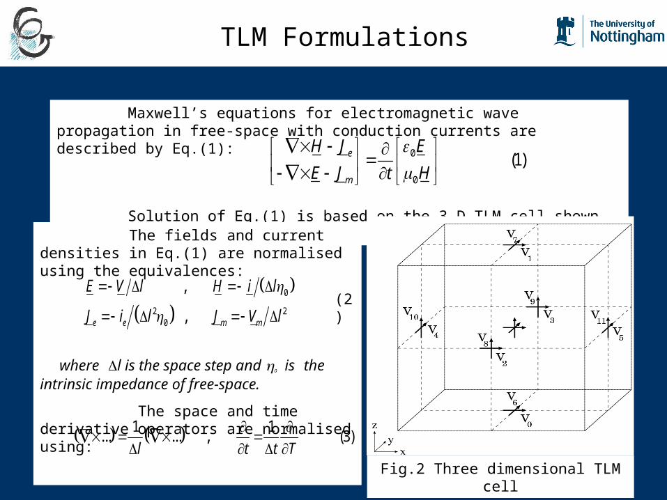
TLM Formulations
Maxwell’s equations for electromagnetic wave propagation in free-space with conduction currents are described by Eq.(1):
Solution of Eq.(1) is based on the 3-D TLM cell shown in Fig.2.
0
0
(1)e
m
H J E
E J Ht
Fig.2 Three dimensional TLM cell
The fields and current densities in Eq.(1) are normalised using the equivalences:
where l is the space step and 0 is the intrinsic impedance of free-space.
The space and time derivative operators are normalised using:
0
2 20
,
,e e m m
E V l H i l
J i l J V l
(2)
1 1... ... , (3)
l t t T

TLM Formulations (continued)
The maximum time-step in the three-dimensional TLM algorithm is t=l/(2c), where c is the speed of light in free-space. If the simulation is iterated at the maximum time-step, in terms of the normalisations Eqs.(2)-(3), Maxwell’s Equations Eq.(1) in free-space could be reduced to,
This set of equations is then mapped into the cell in Fig.2. For free-space modelling with current densities, the calculation of the total fields at the centre of the cell can be expressed as,
where the incident pulses are denoted by the superscript i. The normalised electric conduction currents {iex,iey,iez} are used to describe currents in wires.
2 (4)e
m
i i V
iTV V
0 1 2 3
4 5 6 7
8 9 10 11
6 7 8 9
10 11 0 1
2 3 4 5
1 1(5)
2 4
i i i i
exx i i i i
eyyi i i i
ezz
i i i imxx
i i i i myy
mzzi i i i
V V V ViV
V V V ViV
V V V V iV
Vi V V V VVi
V V V VVi
V V V V

The reflected pulses are obtained from Eq. (6), where superscript r indicating reflection.
TLM Formulations (continued)
10
01
32
23
54
45
76
67
98
89
1110
1011
irx y
irx y
irx z
irx z
iry z
iry z
iry x
iry x
irz x
irz x
irz y
irz y
V i VV
V i VV
V i VV
V i VV
V i VV
V i VV
V i VV
V i VV
V i VV
V i VV
V i VV
V i VV
(6)
At external boundaries of a mesh (for example port 6 at Zmin), a reflection coefficient Rb is specified as,
where, Rb =-1: a perfect electric conductor, Rb=1: a perfect magnetic conductor; Rb=0: a matched boundary, respectively.
For description of frequency-dependent boundaries, Rb may be specified as a frequency-dependent function.
1 6 min 6 min (8)i rk b kV Z R V Z
The incident voltages at the next time-step k+1 are founf by swapping with the reflected voltages at time step k. For example, the swap between ports 0 and 1 of the nodes located at cell indicates Z and Z-1 is,
1 1 0 1 0 11 , 1 (7)i r i rk k k kV Z V Z V Z V Z
For a free-space simulations with current densities, equations (5)-(8) would apply to all nodes and ports in the mesh for the software implementation.

3-D TLM Implementation
To aid the development of the model of field-wire coupling involving an x-directed straight wire, consider the shunt node associated with Vx derided from the 3-D node. Fig.3
shows this node and Fig. 4 shows the equivalent circuit.
Fig.3 Shunt node for evaluation of Vx
The voltage Vx is obtained as,
0 1 2 3 2 4 (9)i i i ix exV V V V V i
Fig.4 Equivalent circuit of a shunt
node describing Vx .

Formulations for Field-Wire Coupling
For straight wires, the telegrapher’s equations describing an x-directed wire may be expressed as Eqs(10)-(11), where Vw is the wire potential, Iwx is the wire current and Lw /l, Rw /l and Cw /l are the wire inductance, resistance and capacitance per unit length respectively. The field-to-wire coupling is in the last terms of Eq.(10).
10
11
w w wx w xwx
wx w w
V L I R VI
x l t l l
I C V
x l t
A 3-D cell containing an x-directed wire is shown in Fig.5, which indicates the voltage pulses {V0, V1, V2 ,V3} interacting with the x-directed wire.
Fig. 5 3-D TLM cell containing an x-directed wire
The wire inductance Lw /l=0kw and wire capacitance Cw /l =0/kw ,where kw is a frequency-independent dimensionless geometrical factor.

Formulations for Field-Wire Coupling (continued)
The velocity of propagation of charge variations along the wire is the speed of light, i.e.
. The characteristic impedance of the wire is . The wire current is normalised using , where iwx has the dimension of volts. The time and space derivative operators are normalised using .
Using the notations given above, Eqs.(10)-(11) may be rewritten as equations (12), where the normalised wire resistance rw=Rw/Zw . Equations (12) may be converted to the travelling wave format equations (13) by using the equivalences Eq.(9),
The TLM equivalent circuit for the discrete-time solution of the equations (10)-(11) can therefore be written as,
w wc l L C 0w w w wZ L C k
wx wx wI i Z1 1
,x l X t t T
2
2 12
w wxw wx x
wx w
V ir i V
X Ti V
X T
4 5
4 5
2 2 2
2 2 2 13
i iw wxw w wx
i iwx ww w w
V iV V i
X Ti V
V V VX T
4 5
4 5
1
0
2 2 2 2
2 2 4 4 14
4 4
i i i xw w w w wLx r
i i iw w w wC
w w w
i T V V V V
V V V V
where T r y

Equivalent Circuit for Field-Wire Coupling
Equivalent circuit for field-wire coupling for an x-directed wire is shown in Fig.6, and the normalised equivalent circuit for field-wire coupling for an x-directed wire is shown in Fig.7.
Fig. 6 Equivalent circuit for field-wire
coupling for an x-directed wire.
Fig. 7 Normalised equivalent circuit for
field-wire coupling for an x-directed wire.

Simulation Results of a Dipole Antenna Coupling to a Thin Wire
The configurations of the simulation models are shown in Fig.1 (a)-(b). The currents on the thin wire at points 25 cm, 50 cm and 75 cm from the junction of the wire, and the feed current at the gap of the dipole antenna excited by a sinusoid of 900 MHz or a Gaussian pulse with a halfwidth of 0.8 nm are calculated in both the parallel and perpendicular cases respectively by TLM method. The simulation results of the current transfer ratio (Iw/I_feed) for both configurations, excited by a sinusoid or a Gaussian function, are listed in Table 1.
Configuration Position to the wire junction (cm)
Sinusoid
Iw /I_feed
Gaussian
Iw/I_feed
Parallel
25
50
75
0.050
0.056
0.056
0.052
0.056
0.056
Perpendicular
25
50
75
0.011
0.0126
0.00467
0.011
0.0128
0.00431
Table1 : Simulation Results of a Dipole Antenna Coupling to a Thin Wire
Table 1 shows the current transfer ratios obtained from the steady-state and pulse excitations are in good agreement. The electromagnetic coupling is greater when a dipole is parallel to a thin wire.

Sinusoid Dipole Coupling to a Thin Wire (Parallel Configuration)
The currents on the thin wire at points 25 cm, 50 cm and 75 cm to the wire junction and the feed current at the gap of the dipole antenna, excited by sinusoid source in a parallel configuration, are calculated and the results are shown in Figs.8(a)-(d). The current transfer ratios at points 25 cm, 50 cm and 75 cm may be obtained from these graphs and listed in Table 1.
Fig.8 Currents excited by a sinusoid dipole parallel to a thin wire:
(a) feed current at the gap of the sinusoid dipole; (b) current on the thin wire at a point 25 cm from the junction ;
(c) current on the thin wire at a point 50 cm from the junction; (d) current on the thin wire at a point 75 cm from the junction
(a) (b)
(c) (d)

The currents on the thin wire at points 25 cm, 50 cm and 75 cm to the wire junction and the feed current at the gap of the dipole antenna, excited by sinusoid source in a perpendicular configuration, are calculated and the results are shown in Figs.9(a)-(d). The current transfer ratios at points 25 cm, 50 cm and 75 cm may be obtained from these graphs and listed in Table 1.
Fig.9 Currents excited by a sinusoid dipole perpendicular to a thin wire:
(a) feed current at the gap of the sinusoid dipole; (b) current on the thin wire at a point 25 cm from the junction ;
(c) current on the thin wire at a point 50 cm from the junction; (d) current on the thin wire at a point 75 cm from the junction.
Sinusoid Dipole Coupling to a Thin Wire (Perpendicular Configuration)
(a) (b)
(c) (d)

Hz Field Distribution in the Dipole-Thin Wire Plane

Fast Fourier Transform Analyses Results
The current transfer ratios at points 25cm, 50cm and 75cm on the thin wire excited by a Gaussian function are obtained for both the parallel and perpendicular configurations respectively. Results obtained over the frequency range 600-1200 MHz are shown in Figs.10 (a)-(f).
(a) (b) (c)
(d) (e) (f)
Fig.10 FFT analyses of the thin wire coupling to a dipole antenna excited by a Gaussian function in both parallel and perpendicular cases:
Parallel case: (a) Current transfer ratio at 25cm; (b) Current transfer ratio at 50cm; (c) Current transfer ratio at 75cm;
Perpendicular case: (a) Current transfer ratio at 25cm; (b) Current transfer ratio at 50cm; (c) Current transfer ratio at 75cm.
The thin-wire formulation technique employed here to simulate this problem is based on a quasi-static solution for the field around the wire. This is a symmetrical solution and therefore can only be used to place the wire centrally in the a computational cell. In cases where an offset wire description is required a more complete solution may be used which takes account of more modes (not just the quasi-static term included by Holland and Simpson) in the wire solution. The total field at the sampling points of the computational cell is decomposed into its modal components, these are then reflected by the correct modal impedance (see next slide) and then re-combined to obtain the reflected total field for transmission to the rest of the numerical solution.

T h e r e a s o n t h a t t h e H o l l a n d a n d S i m p s o n t y p e o f a p p r o a c h i s i n a c c u r a t e i s t h a t t h e r e i s i n s u f f i c i e n t i n f o r m a t i o n c o n t a i n e d i n t h e q u a s i - s t a t i c s o l u t i o n f o r a w i r e . T h e g e n e r a l r e s p o n s e o f a w i r e t o a n i n c i d e n t f i e l d i s t o g e n e r a t e a s c a t t e r e d f i e l d w h i c h i n c o m b i n a t i o n w i t h t h e i n c i d e n t f i e l d i s r i c h i n m o d a l i n f o r m a t i o n :
00 0
0
0
( )( , ) ( ) ( ) ( 1 5 )
( )
1( , ) ( 1 6 )
j nz n n n
n n
z
J k aE r B e J k r N k r
N k a
EH r
j r
T h e s t a t i c s o l u t i o n i s b u t t h e f i r s t t e r m i n t h i s e x p a n s i o n - b u t t h e r e i s m u c h m o r e i n f o r m a t i o n
a v a i l a b l e ! T h e i m p e d a n c e s e e n b y e a c h m o d e m a y b e o b t a i n e d f r o m t h e e x p r e s s i o n a b o v e E / H .
““An accurate thin-wire model for 3D TLM An accurate thin-wire model for 3D TLM simulation”, P Sewell, Y K Choong, C simulation”, P Sewell, Y K Choong, C Christopoulos, TEMC Trans on EMC, Christopoulos, TEMC Trans on EMC, 45(2), 2003, pp 207-21745(2), 2003, pp 207-217

Magnitude of the electric field observed 2 and 8 nodes in front of the node containing three dielectric coated wires when excited by a plane wave.

Conclusions
The electromagnetic coupling of a half wave dipole antenna to a thin wire is simulated using the TLM method. Two configurations of the dipole positions are considered, in which the antenna is positioned either parallel to, or perpendicular to, the thin wire. Results obtained by using the steady-state and pulse excitations agree closely.
Results are obtained by combining the versatility of the TLM with the efficiency of powerful thin-wire formulations.


![- [Book] the TLM Method in Electromagnetics (C. Christopoulos 2006)](https://img.pdfslide.us/doc/110x75/577d1f1c1a28ab4e1e8fe5a0/-book-the-tlm-method-in-electromagnetics-c-christopoulos-2006.jpg)