Embed Size (px)
Citation preview
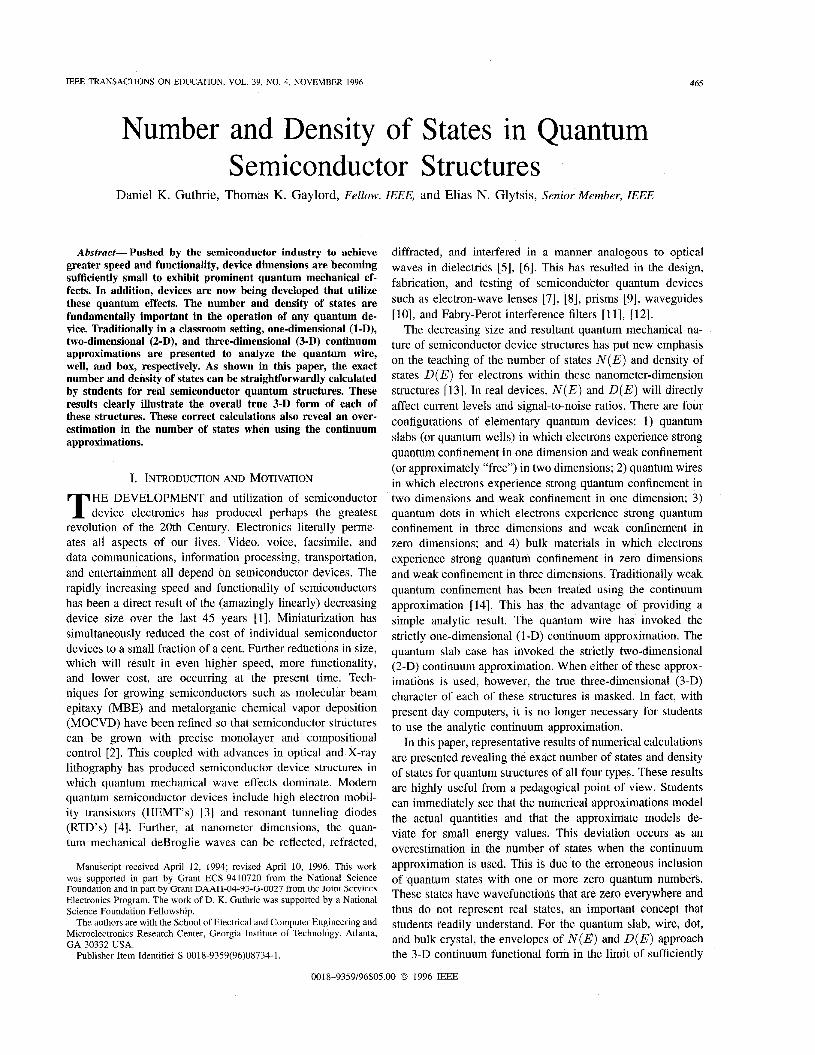
IEEE TRANSACTIONS ON EDUCATION, VOL. 39, NO. 4, NOVEMBER 1996 465
Number and Density of States in Quantum - * Semiconductor Structures Daniel K. Guthrie, Thomas K. Gaylord, Fellow, ZEEE, and Elias N. Glytsis, Senior Member, ZEEE
Abstract- Pushed by the semiconductor industry to achieve greater speed and functionality, device dimensions are becoming sufficiently small to exhibit prominent quantum mechanical ef- fects. In addition, devices are now being developed that utilize these quantum effects. The number and density of states are fundamentally important in the operation of any quantum de- vice. Traditionally in a classroom setting, one-dimensional (1-D), two-dimensional (2-D), and three-dimensional (3-D) continuum approximations are presented to analyze the quantum wire, well, and box, respectively. As shown in this paper, the exact number and density of states can be straightforwardly calculated by students for real semiconductor quantum structures. These results clearly illustrate the overall true 3-D form of each of these structures. These correct calculations also reveal an over- estimation in the number of states when using the continuum approximations.
I. INTRODUCTION AND MOTIVATION
HE DEVELOPMENT and utilization of semiconductor T device electronics has produced perhaps the greatest revolution of the 20th Century. Electronics literally perme- ates all aspects of our lives. Video, voice, facsimile, and data communications, information processing, transportation, and entertainment all depend on semiconductor devices. The rapidly increasing speed and functionality of semiconductors has been a direct result of the (amazingly linearly) decreasing device size over the last 45 years [l]. Miniaturization has simultaneously reduced the cost of individual semiconductor devices to a small fraction of a cent. Further reductions in size, which will result in even higher speed, more functionality, and lower cost, are occurring at the present time. Tech- niques for growing semiconductors such as molecular beam epitaxy (MBE) and metalorganic chemical vapor deposition (MOCVD) have been refined so that semiconductor structures can be grown with precise monolayer and compositional control [2]. This coupled with advances in optical and X-ray lithography has produced semiconductor device structures in which quantum mechanical wave effects dominate. Modern quantum semiconductor devices include high electron mobil- ity transistors (HEMT’s) 131 and resonant tunneling diodes (RTD’s) [4]. Further, at nanometer dimensions, the quan- tum mechanical deBroglie waves can be reflected, refracted,
Manuscript received April 12, 1994; revised April 10, 1996. This work was supported in part by Grant ECS-9410720 from the National Science Foundation and in pdrt by Grdnt DAAH-04-93-G-0027 from the Joint Services Electronics Program. The work of D K Guthrie was supported by a National Science Foundation Fellowship.
The authors are with the School of Electrical and Computer Engineering and Microelectronics Research Center, Georgia Institute of Technology, Atlanta, GA 30332 USA
Publisher Item Identifier S 0018-9359(96)08734-1
0018-9359/96$05
diffracted, and interfered in a manner analogous to optical waves in dielectrics 151, [6]. This has resulted in the design, fabrication, and testing of semiconductor quantum devices such as electron-wave lenses [7], [8], prisms [9], waveguides [lo], and Fabry-Perot interference filters [ 111, [ 121.
The decreasing size and resultant quantum mechanical na- ture of semiconductor device structures has put new emphasis on the teaching of the number of states N ( E ) and density of states D( E ) for electrons within these nanometer-dimension structures [13]. In real devices, N ( E ) and D ( E ) will directly affect current levels and signal-to-noise ratios. There are four configurations of elementary quantum devices: 1) quantum slabs (or quantum wells) in which electrons experience strong quantum confinement in one dimension and weak confinement (or approximately “free”) in two dimensions; 2) quantum wires in which electrons experience strong quantum confinement in two dimensions and weak confinement in one dimension; 3) quantum dots in which electrons experience strong quantum confinement in three dimensions and weak confinement in zero dimensions; and 4) bulk materials in which electrons experience strong quantum confinement in zero dimensions and weak confinement in three dimensions. Traditionally weak quantum confinement has been treated using the continuum approximation 1141. This has the advantage of providing a simple analytic result. The quantum wire has invoked the strictly one-dimensional (1 -D) continuum approximation. The quantum slab case has invoked the strictly two-dimensional (2-D) continuum approximation. When either of these approx- imations is used, however, the true three-dimensional (3-D) character of each of these structures is masked. In fact, with present-day computers, it is no longer necessary for students to use the analytic continuum approximation.
In this paper, representative results of numerical calculations are presented revealing the exact number of states and density of states for quantum structures of all four types. These results are highly useful from a pedagogical point of view. Students can immediately see that the numerical approximations model the actual quantities and that the approximate models de- viate for small energy values. This deviation occurs as an overestimation in the number of states when the continuum approximation is used. This is due to the erroneous inclusion of quantum states with one or more zero quantum numbers. These states have wavefunctions that are zero everywhere and thus do not represent real states, an important concept that students readily understand. For the quantum slab, wire, dot, and bulk crystal, the envelopes of N ( E ) and D ( E ) approach the 3-D continuum functional form in the limit of sufficiently
.OO 0 1996 IEEE
466 IEEE TRANSACTIONS ON EDUCATION, VOL. 39, NO. 4, NOVEMBER 1996
/ 4-
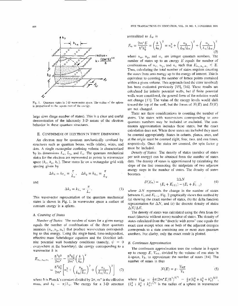
Fig. 1. is proportional to the square root of the energy.
Quantum states in 3-D wavevector space. The radius of the sphere
large sizes (large number of states). This is a clear and useful demonstration of the inherently 3-D nature of the electron behavior in these quantum structures.
11. CONFINEMENT OF ELECTRON IN THREE DIMENSIONS
An electron may be quantum mechanically confined by structures such as quantum boxes, wells (slabs), wires, and dots. A single rectangular confining volume is characterized by its dimensions Lz , Ly, and L,. The quantum mechanical states for the electron are represented as points in wavevector space ( k, , k,, k,). These states lie on a rectangular grid with spacing given by
n ?T Ak, = IcL, = -, Ak, = kL,, = - L X LY
and
Ak, = kLz = L. (1) L, This wavevector representation of the quantum mechanical states is shown in Fig. 1. In wavevector space a surface of constant energy is a sphere.
A. Counting of States Number of States: The number of states for a given energy
equals the number of combinations of the three quantum numbers (n,, n, , n,) that produce wavevectors correspond- ing to that energy. Using the single-band, time-independent, effective-mass Schrodinger equation and the Dirichlet infi- nite potential wall boundary conditions (namely, $I = 0 everywhere at the boundary), the energy corresponding to a wavevector k is
normalized to L, is
where nz, nu, and n, are integer quantum numbers. The number of states up to an energy E equals the number of combinations of n,, ny, and n, such that Enz,ny,nz 5 E. Thus, calculating the total number of states requires counting the states from zero energy up to the energy of interest. This is equivalent to counting the number of lattice points contained within a given volume. This approach (and the error involved) has been evaluated previously [15], [16]. These results are calculated for infinite potential walls, but if finite potential walls were considered, the general form of the solution would not change [17]. The value of the energy levels would shift toward the top of the well, but the forms of N ( E ) and D ( E ) are not changed.
There are three considerations in counting the number of states. The states with wavevectors corresponding to zero quantum numbers may be included or excluded. The con- tinuum approximation includes these states, but the exact calculation does not. When these states are included they must be counted appropriately. States in octants, planes, axes, and at the origin must be counted eight, four, two, and one times, respectively. Once the states are counted, the spin factor g must be included.
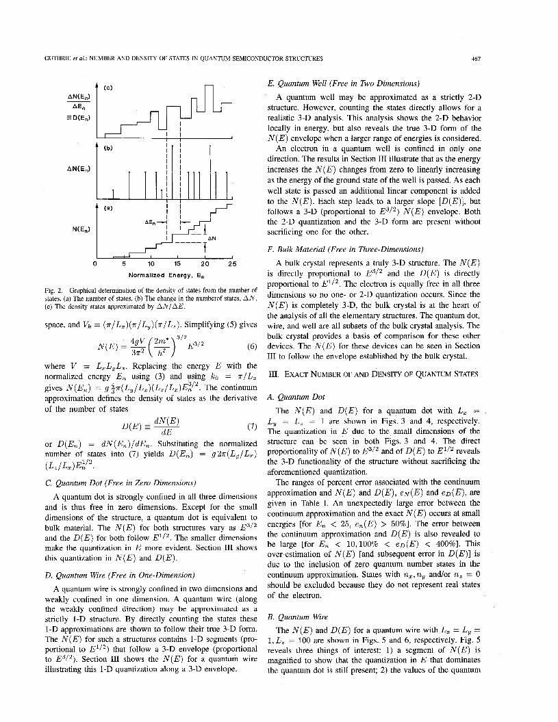
Density of States: The density of states (number of states per unit energy) can be obtained from the number of states data. The density of states is approximated by calculating the slope of the line connecting the midpoints of two adjacent energy steps in the number of states. The density of states becomes
where A N represents the change in the number of states between E, and E,+1. Fig. 2 graphically shows this method by (a) showing the exact number of states, (b) the delta function representation for AN, and (c) the discrete density of states ANlAE.
The density of states was calculated using the data from the exact (discrete without zeros) number of states. The density of states calculated from the “discrete with zeros” case equals the exact case except when one or both of the adjacent energies corresponds to a state containing one or more zero quantum numbers. For clarity, only the exact result is plotted.
B. Continuum Approximation The continuum approximation uses the volume in k-space
up to energy E , V ~ E , divided by the volume of one state in Ic-space, V k , to approximate the number of states [14]. The number of states is thus
where TL is Planck’s constant divided by 2n, m* is the effective mass, and ko = TIL,. The energy for a 3-D structure
where V ~ E = $ ~ ( 2 m * E / f L ~ ) ~ / ’ = $n(kz + k i + Ic22)3’2 , ( I c ; + k i + k2)1/2 is the radius of a sphere in wavevector
GUTHRIE et al.: NUMBER AND DENSITY OF STATES IN QUANTUM SEMICONDUCTOR STRUCTURES 461
/ I ----- I T I I
0 5 10 15 20 25
Normalized Energy, E,
Fig. 2. Graphical determination of the density of states from the number of states. (a) The number of states. (b) The change in the numberof states, AN. (c) The density states approximated by AN/AE.
space, and V k = (r/Lx)(7r/Ly)(7r/Lz). Simplifying (5) gives
where V = L,L,L,. Replacing the energy E with the normalized energy E, using (3) and using IC0 = r / L , gives N(E,) = g $T(L,/L,)(L,/L,)E~/'. The continuum approximation defines the density of states as the derivative of the number of states
(7)
or D(E,) = dN(E,)/dE,. Substituting the normalized number of states into (7) yields D(E,) = g2r(L,/LX) (L,/L,)EA/'. C. Quantum Dot {Free in Zero Dimensions)
A quantum dot is strongly confined in all three dimensions and is thus free in zero dimensions. Except for the small dimensions of the structure, a quantum dot is equivalent to bulk material. The N ( E ) for both structures vary as E3l2 and the D ( E ) for both follow The smaller dimensions make the quantization in E more evident. Section I11 shows this quantization in N ( E ) and D ( E ) .
D. Quantum Wire (Free in One-Dimension)
A quantum wire is strongly confined in two dimensions and weakly confined in one dimension. A quantum wire (along the weakly confined direction) may be approximated as a strictly 1-D structure. By directly counting the states these 1-D approximations are shown to follow their true 3-D form. The N ( E ) for such a structures contains 1-D segments (pro- portional to @/') that follow a 3-D envelope (proportional to E3/'). Section I11 shows the N ( E ) for a quantum wire illustrating this 1-D quantization along a 3-D envelope.
E. Quantum Well {Free in Two Dimensions)
A quantum well may be approximated as a strictly 2-D structure. However, counting the states directly allows for a realistic 3-D analysis. This analysis shows the 2-D behavior locally in energy, but also reveals the true 3-D form of the N ( E ) envelope when a larger range of energies is considered.
An electron in a quantum well is confined in only one direction. The results in Section I11 illustrate that as the energy increases the N ( E ) changes from zero to linearly increasing as the energy of the ground state of the well is passed. As each well state is passed an additional linear component is added to the N ( E ) . Each step leads to a larger slope [D(E)] , but follows a 3-D (proportional to E3l2 ) N ( E ) envelope. Both the 2-D quantization and the 3-D form are present without sacrificing one for the other.
F. Bulk Material (Free in Three-Dimensions)
A bulk crystal represents a truly 3-D structure. The N ( E ) is directly proportional to E3I2 and the D ( E ) is directly proportional to The electron is equally free in all three dimensions so no one- or 2-D quantization occurs. Since the N ( E ) is completely 3-D, the bulk crystal is at the heart of the analysis of all the elementary structures. The quantum dot, wire, and well are all subsets of the bulk crystal analysis. The bulk crystal provides a basis of comparison for these other devices. The N ( E ) for these devices can be seen in Section I11 to follow the envelope established by the bulk crystal.
111. EXACT NUMBER OF AND DENSITY OF QUANTUM STATES
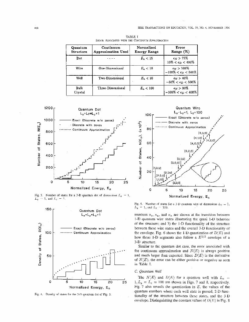
A. Quantum Dot The N ( E ) and D ( E ) for a quantum dot with L, =
L, = L, = 1 are shown in Figs. 3 and 4, respectively. The quantization in E due to the small dimensions of the structure can be seen in both Figs. 3 and 4. The direct proportionality of N ( E ) to E3/' and of D ( E ) to El/' reveals the 3-D functionality of the structure without sacrificing the aforementioned quantization.
The ranges of percent error associated with the continuum approximation and N ( E ) and D( E ) , e N ( E ) and e o ( E ) , are given in Table I. An unexpectedly large error between the continuum approximation and the exact N ( E ) occurs at small energies [for E, < 25, e,(E) > 50%]. The error between the continuum approximation and D ( E ) is also revealed to be large [for E, < 10,100% < e o ( E ) < 400%]. This over-estimation of N ( E ) [and subsequent error in D ( E ) ] is due to the inclusion of zero quantum number states in the continuum approximation. States with n,, ny and/or n, = 0 should be excluded because they do not represent real states of the electron.
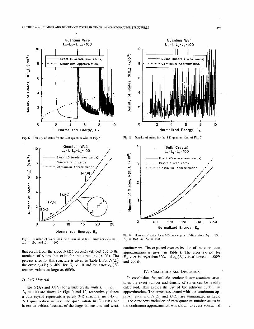
B. Quantum Wire The N ( E ) and D ( E ) for a quantum wire with L, = L, =
1, L, = 100 are shown in Figs. 5 and 6, respectively. Fig. 5 reveals three things of interest: 1) a segment of N ( E ) is magnified to show that the quantization in E that dominates the quantum dot is still present; 2) the values of the quantum
468
Quantum Structure
Dot
Wire
IEEE TRANSACTIONS ON EDUCATION, VOL. 39, NO. 4, NOVEMBER 1996
Continuum Normalized Error Approximation Used Energy Range Range (%)
_ _ - _ E,, < 15 e N > 75%
One-Dimensional E,, < 10 e N > 100% 10% < eo < 400%
-100% < e g < 500%
TABLE I ERROR ASSOCIATED WT'H THE CONTINUUM APPROXIMATION
Well
Bulk Crystal
1200
Two-Dimensional E,, < 10 e N > 40%
Three-Dimensional E, < 100 e N > 30%
-50% < eg < 500%
-100% < e g < 400%
1000 CI c
w Y
800 CO (U
Q CI
fj 600 'c 0
400 n
z f 200
0
Q u a n t u m Dot Lx= LY L, = 1
Exact (Discrete w /o zeros) '
Discrete with zeros -_ * * * * . * * * * Continuum Approximation
. f '
5 10 15 20 25 Normalized Energy, E,
Fig. 3 L, = 1, and L, = 1.
Number of states for a 3-D quantum dot of dimensions L , r 1,
h I C
v W 0 100 d
5 j
a, m c
Q u a n t u m Dot Lx= L, = L, = 1
Exact (Discrete w /o zeros) . . . . . . . . . Continuum Approximation
0 x
I I I I
0 5 10 15 20 25 Normalized Energy, E,
Fig. 4. Density of states for the 3-D quantum dot of Fig. 3.
Q u a n t u m Wire
Exact (Discrete w /o zeros)
L x = L y = I r L z = l O O
_ _ Discrete with zeros . . . . . . 1 . . Continuum Approximation
0 5 10 15 20 25
Normalized Energy, E,
Fig. 5. Number of states for a 3-D quantum wire of dimensions L, = 1, L , = 1, and L, = 100.
numbers n,, ny, and n, are shown at the transition between 1-D quantum wire states illustrating the quasi 1-D behavior of the structure; and 3) the 1-D functionality of the structure between these wire states and the overall 3-D functionality of the envelope. Fig. 6 shows the 1-D quantization of D ( E ) and how these 1-D segments also follow a Ell2 envelope of a 3-D structure.
Similar to the quantum dot case, the error associated with the continuum approximation and N ( E ) is always positive and much larger than expected. Since D ( E ) is the derivative of N ( E ) , the error can be either positive or negative as seen in Table I.
C. Quantum Well
The N ( E ) and D ( E ) for a quantum well with L, = 1, L, = L, = 100 are shown in Figs. 7 and 8, respectively. Fig. 7 also reveals the quantization in E , the values of the quantum numbers where each well state is passed, 2-D func- tionality of the structure between these states, and the 3-D envelope. Distinguishing the constant values of D ( E ) in Fig. 8
GUTHRIE et al.: NUMBER AND DENSITY OF STATES IN QUANTUM SEMICONDUCTOR STRUCTURES 469
n m e X
n c
Y
Y
w d i a (d c.
I5 IC 0
r. U) C a L3
c .-
Fig. 6.
h W
X Y
n C
w v z
Q m i c.
z r 0
a L
n 5 z
10
8
6
4
2
0
Quantum Wire L x = L y = l , L z . 1 0 0
I YI Exact (Discrete w/o zeros)
I ..-.*..-. Continuum Approximation I I
2 4 6 8 10 Normalized E n e r g y , E n
Density of states for the 3-D quantum wire of Fig. 5.
10
8
6
4
2
0
Quantum Well Lx=l , L y = L , = I 0 O
Exact (Discrete w l o zeros)
Discrete with zeros _ _ ..*-...-- Continuum Approximation
5 10 15 20 25
Normalized Energy, En
Fig. 7. L, = 100, and L, = 100.
Number of states for a 3-D quantum slab of dimensions L , = 1,
that result from the slope N ( E ) becomes difficult due to the numbers of states that exist for this structure (>lo7). The percent error for this structure is given in Table I. For N ( E ) the error e N ( E ) > 40% for E, < 10 and the error eo(E) reaches values as large as 600%.
D. Bulk Material
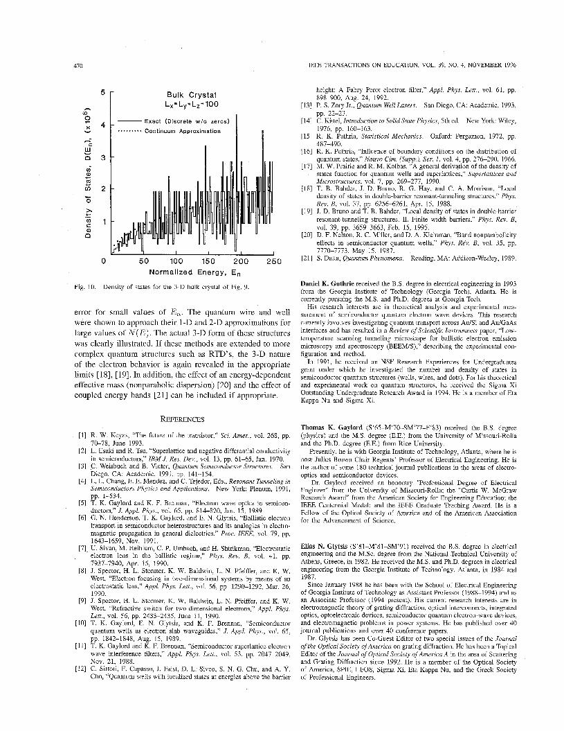
The N ( E ) and D ( E ) for a bulk crystal with L, = L, = L, = 100 are shown in Figs. 9 and 10, respectively. Since a bulk crystal represents a purely 3-D structure, no 1-D or 2-D quantization occurs. The quantization in E exists but is not as evident because of the large dimensions and weak
n v)
s X Y
c5 C
W Y n U) a m +
z c 0 x U) C 0
c .-
n
Fig. 8.
n b) :
X v
n C
v w z U) a m c G .+ 0
Q) L
n f z
10
8
6
4
2
0
Q u a n t u m Well L x = l , Ly=L,= lOO
Exact (Discrete w l o zeros)
*.....**. Continuum Approximation
2 4 6 8 10 Normalized E n e r g y , E n
Density of states for the 3-D quantum slab of Fig. 7.
Bulk C r y s t a l Lx= Ly = L,= 100
Exact (Discrete w / o zeros) .- Discrete with zeros ___
50 100 150 200 250 Normalized E n e r g y , E n
Fig. 9. L, = 100, and L , = 100.
Number of states for a 3-D bulk crystal of dimensions L , = 100,
confinement. The expected over-estimation of the continuum approximation is given in Table I. The error eN(E) for E, < 50 is larger than 50% and e o ( E ) varies between - 100% and 200%.
Iv. CONCLUSION AND DISCUSSION
In conclusion, for realistic semiconductor quantum struc- tures the exact number and density of states can be readily calculated. This avoids the use of the artificial continuum approximation. The errors associated with the continuum ap- proximation and N ( E ) and D ( E ) are summarized in Table I. The erroneous inclusion of zero quantum number states in the continuum approximation was shown to cause substantial
470 IEEE TRANSACTIONS ON EDUCATION, VOL. 39, NO. 4, NOVEMBER 1996
Bulk Crystal Lx= L,=L,= 100
00 Exact (Discrete w / o zeros)
. . . . . . . . . Continuum Approximation Y
C
v w 0 3 v) W c
z 2 c 0 2. c .- * l
n C a
0 50 100 150 200 250 Normalized Energy , En
Fig. 10. Density of states for the 3-D bulk crystal of Fig. 9.
error for small values of E,. The quantum wire and well were shown to approach their 1-D and 2-D approximations for large values of N ( E ) . The actual 3-D form of these structures was clearly illustrated. If these methods are extended to more complex quantum structures such as RTD’s, the 3-D nature of the electron behavior is again revealed in the appropriate limits [ 181, [ 191. In addition, the effect of an energy-dependent effective mass (nonparabolic dispersion) [20] and the effect of coupled energy bands [21] can be included if appropriate.
REFERENCES
111 R. W. Keyes, “The future of the transistor,” Sci. Amer., vol. 268, DD. . .
70-78, June 1993. 121 L. Esaki and R. Tsu. “Suoerlattice and negative differential conductivitv _ _
in s e m i c o n d u c t o r s , ~ ~ ’ l ~ ~ J. Res. Dev., v;. 13, pp. 61-65, Jan. 1970. ‘ [3] C. Weisbuch and B. Vinter, Quantum Semiconductor Structures. San
Diego, CA: Academic, 1991, pp. 141-154. [4] L. L. Chang, E. E. Mendez, and C. Tejedor, Eds., Resonant Tunneling in
Semiconductors Physics and Applications. New York: Plenum, 199 1, pp. 1-534.
[5] T. K. Gaylord and K. F. Brennan, “Electron wave optics in semicon- ductors,” J. Appl. Phys., vol. 65, pp. 814-820, Jan. 15, 1989.
[6] G. N. Henderson, T. K. Gaylord, and E. N. Glytsis, “Ballistic electron transport in semiconductor heterostructures and its analogies in electro- magnetic propagation in general dielectrics,” Proc. IEEE, vol. 79, pp.
[7] U. Sivan, M. Heiblum, C. P. Umbach, and H. Shtrikman, “Electrostatic electron lens in the ballistic regime,” Phys. Rev. B, vol. 41, pp. 7937-7940, Apr. 15, 1990.
[8] J. Spector, H. L. Stormer, K. W. Baldwin, L. N. Pfeiffer, and K. W. West, “Electron focusing in two-dimensional systems by means of an electrostatic lens,” Appl. Phys. Lett., vol. 56, pp. 1290-1292, Mar. 26, 1990.
[9] J. Spector, H. L. Stormer, K. W. Baldwin, L. N. Pfeiffer, and K. W. West, “Refractive switch for two-dimensional electrons,” Appl. Phys. Lett., vol. 56, pp. 2433-2435, June 11, 1990.
[lo] T. K. Gaylord, E. N. Glytsis, and K. F. Brennan, “Semiconductor quantum wells as electron slab waveguides,” J. Appl. Phys., vol. 65,
[11] T. K. Gaylord and K. F. Brennan, “Semiconductor superlattice electron wave interference filters,” Appl. Phys. Lett., vol. 53, pp. 2047-2049, Nov. 21, 1988.
1121 C. Sirtori, F. Capasso, J. Faist, D. L. Sivco, S. N. G. Chu, and A. Y. Cho, “Quantum wells with localized states at energies above the barrier
1643-1659, NOV. 1991.
pp. 1842-1848, Aug. 15, 1989.
height: A Fabry Perot electron filter,” Appl. Phys. Len., vol. 61, pp. 898-900, Aug. 24, 1992.
[13] P. S. Zory Jr., Quantum Well Lasers. San Diego, CA: Academic, 1993, pp. 22-23.
1141 C. Kittel, Introduction to Solid State Physics, 5th ed. New York: Wiley, . .
1976, pp. 160-163. [15] R. K. Pathria, Statistical Mechanics. Oxford: Pergamon, 1972, pp.
487490. [ 161 R. K. Pathria, “Influence of boundary conditions on the distribution of
quantum states,” Nouvo Cim. (Supp.), Ser. 1, vol. 4, pp. 276-290, 1966. [17] M. W. Prairie and R. M. Kolbas, “A general derivation of the density of
states function for quantum wells and superlattices,” Superlattices and Microstructures, vol. 7, pp. 269-217, 1990.
[18] T. B. Bahder, J. D. Bruno, R. G. Hay, and C. A. Morrison, “Local density of states in double-barrier resonant-tunneling structures,” Phys. Rev. B , vol. 37, pp. 6256-6261, Apr. 15, 1988.
[19] J. D. Bruno and T. B. Bahder, “Local density of states in donble-barrier resonant-tunneling structures. 11. Finite width barriers,” Phys. Rev. B , vol. 39, pp. 3659-3663, Feb. 15, 1995.
[20] D. F. Nelson, R. C. Miller, and D. A. Kleinman, “Band nonparabolicity effects in semiconductor quantum wells,” Phys. Rev. B, vol. 35, pp. 7770-7773, May 15, 1987.
[21] S. Datta, Quantum Phenomena. Reading, MA: Addison-Wesley, 1989.
Daniel K. Guthrie received the B.S. degree in electrical engineering in 1993 from the Georgia Institute of Technology (Georgia Tech), Atlanta. He is currently pursuing the M.S. and Ph.D. degrees at Georgia Tech.
His research interests are in theoretical analysis and experimental mea- surement of semiconductor quantum electron wave devices. This research currently involves investigating quantum transport across Au/Si and Au/GaAs interfaces and has resulted in a Review ofScient$c Znstruments paper, “Low- temperature scanning tunneling microscope for ballistic electron emission microscopy and spectroscopy (BEEMIS),” describing the experimental con- figuration and method.
In 1991, he received an NSF Research Experiences for Undergraduates grant under which he investigated the number and density of states in semiconductor quantum structures (wells, wires, and dots). For his theoretical and experimental work on quantum structures, he received the Sigma Xi Outstanding Undergraduate Research Award in 1994. He is a member of Eta Kappa Nu and Sigma Xi.
Thomas K. Gaylord (S‘65-M‘7O-SM‘77-Fi83) received the B.S. degree (physics) and the M.S. degree (E.E.) from the University of Missouri-Rolla and the Ph.D. degree (E.E.) from Rice University.
Presently, he is with Georgia Institute of Technology, Atlanta, where he is now Julius Brown Chair Regents’ Professor of Electrical Engineering. He is the author of some 180 technical journal publications in the areas of electro- optics and semiconductor devices.
Dr. Gaylord received an honorary “Professional Degree of Electrical Engineer” from the University of Missouri-Rolla; the “Curtis W. McGraw Research Award” from the American Society for Engineering Education; the IEEE Centennial Medal; and the IEEE Graduate Teaching Award. He is a Fellow of the Optical Society of America and of the American Association for the Advancement of Science.
Elias N. Glytsis (S’81-M’8l-SM’91) received the B.S. degree in electrical engineering and the M.Sc. degree from the National Technical University of Athens, Greece, in 1982. He received the M.S. and Ph.D. degrees in electrical engineering from the Georgia Institute of Technology, Atlanta, in 1984 and 1987.
Since January 1988 he has been with the School of Electrical Engineering of Georgia Institute of Technology as Assistant Professor (1988-1994) and as an Associate Professor (1994-present). His current research interests are in electromagnetic theory of grating diffraction, optical interconnects, integrated optics, optoelectronic devices, semiconductor quantum electron-wave devices, and electromagnetic problems in power systems. He has published over 40 journal publications and over 40 conference papers.
Dr. Glytsis has been Co-Guest Editor of two special issues of the Joumal of the Optical Society ofAmerica on grating diffraction. He has been a Topical Editor of the Journal of Optical Society of America A in the area of Scattering and Grating Diffraction since 1992. He is a member of the Optical Society of America, SPIE, LEOS, Sigma Xi, Eta Kappa Nu, and the Greek Society of Professional Engineers.


![[Quantum Electronics] Ch-9 Semiconductor Laser-1](https://img.pdfslide.us/doc/110x75/577ce3fe1a28abf1038d78ba/quantum-electronics-ch-9-semiconductor-laser-1.jpg)

![[Quantum Electronics] Ch-9 Semiconductor Laser-2](https://img.pdfslide.us/doc/110x75/577ce3fe1a28abf1038d78e8/quantum-electronics-ch-9-semiconductor-laser-2.jpg)