Embed Size (px)
Citation preview

Prof. dr. ing. D.H.A. Blank Dr. ing. A.J.H.M. Rijnders Dr. H. Schönherr ir. J.J. Broekmaat ir. D.B. Bijl
Nucleation and growth on SrTiO3 substrates characterize
by ex-situ AFM
A.H.G. Prinsen At the Inorganic Materials Science Group
January 2007
9 January 2007


Abstract Nucleation and growth on SrTiO3 substrates characterized by ex-situ AFM
By Bart Prinsen (s0001465)
Since the dimensions of electronic devices are shrinking constantly, approaching the nanometer scale, detailed knowledge of the fundamental growth processes is desirable. Therefore nucleation and growth studies are needed.
In this thesis the parameters for TiO2 island formation on SrTiO3 (STO) substrates using Pulsed Laser Deposition (PLD) are described. Ex-situ AFM was used to study the TiO2 nucleation and growth on STO. Previous experiments showed dentricic shaped island growth of TiO2 on TiO2-terminated STO, which is caused by the non-wetting behavior of B-material on B-sites. Studying TiO2 is interesting, also because of its catalytic properties. These are optimal when the TiO2 has the anatase phase.
Since the substrate surface structure effects the initial growth and nucleation the standard surface treatment for STO has been expanded, tested and adapted for low miscut substrates. To obtain single terminated STO substrates, an etch procedure using a buffered NH4F-HF (BHF) solution is performed. This treatment is successful for high miscut STO substrates, but turns out to be inadequate for low miscut samples. Unit-cell deep holes and mixed termination are encountered problems. The addition of a pre-annealing step at 950 °C improves the substrate quality, resulting in reproducible results and substrates suitable for TiO2 nucleation and growth studies.
To study nucleation and growth it is preferably to do this with real-space imaging techniques, in-situ and at deposition conditions. For this purpose an experimental setup is build. A low thermal mass heater is used in this setup, making AFM imaging at high temperatures and sample quenching possible. The heated filament is a Pt200 and this gives the possibility to read out the temperature while heating. To verify the resistance versus temperature curve and compare this heater with other hot stages in the AFM-field the resistive heater has been calibrated using a pyrometer.
The problems, mentioned above, for the surface treatment hampered the study on the nucleation and growth of TiO2; since single terminated STO substrates with low step density are needed for this. Still optimal parameters have been identified: a) deposition temperatures in the range 700-900 °C, In this temperature range diffusion starts to play a profound role b) at the deposition conditions used deposition of 0 to <40 pulses of material, in this range individual clusters can be observed, after this clusters start to coalesce.
In conclusion: the surface treatment for STO has been adapted for low miscut substrates, providing substrates with single-termination and hole-free areas suitable for TiO2 non-closed monolayer deposition. Interesting parameters have been identified for the TiO2 deposition for further nucleation and growth studies. And finally the low thermal mass heaters have been calibrated, making the PLD-in-situ AFM setup more suitable for future nucleation and growth studies.

Table of Contents
Abstract 1
Table of Contents 2
1 Introduction 5
2 Theoretical Background 8 2.1 Nucleation and Growth of Clusters 8
2.1.1 Crystal Growth 8 2.1.2 Atomic Force Microscopy 10 2.1.3 Quasi Real-time AFM During Pulsed Laser Deposition 10
2.2 Radiation Pyrometry 12 2.3 The Surface Treatment of SrTiO3 13 2.4 Titanium Dioxide, TiO2 14
3 Experimental 17 3.1 Substrate Cutting 17 3.2 Etching and Annealing of Substrates 17 3.3 Pulsed Laser Deposition 18
3.3.1 Principles 18 3.3.2 Setup 19 3.3.3 Depositions in the PLD-RHEED System 19
3.4 Heater Calibration 20
4 Results 21 4.1 Surface Treatment 21
4.1.1 30 Seconds Etching, Annealing at 900 °C 24 4.1.2 Changing the Annealing Temperature, 900 950 °C 25 4.1.3 Increasing Etch Time; 60, 90, 120 sec 26 4.1.4 Pre-annealing 26
4.2 Radiation Pyrometry 27 4.2.1 Determination of ε 27 4.2.2 Heater Calibration 28

1 Introduction 3
4.3 Nucleation and Growth of TiO2 on SrTiO3 30
5 Discussion 35 5.1 Surface Treatment 35 5.2 Radiation Pyrometry 36 5.3 Nucleation and Growth 37
6 Summary and Recommendations 40 6.1 Surface Treatment 40 6.2 Heater Calibration 40 6.3 Nucleation and Growth 41
Acknowledgements 42
References 43
A Original Assignment 44
B Substrate Treatment 45
C AFM Images After Deposition 49
D Hystograms Cluster Height and Area 51
Symbols 55
Distribution List 56


1 Introduction Physical properties of nanoclusters can differ from bulk properties giving rice to interesting properties for catalytic, electrical and magnetic applications, e.g. where bulk gold has no catalytic properties, nanocrystals of gold on oxide surfaces present high reactivity with various gases [1,2,3]. To apply nanocrystals in devices a fundamental understanding of the nucleation and growth of nanoclusters is necessary. Several experimental parameters can be used to control and influence the surface structure. To create nanoclusters different deposition techniques can be used e.g. like molecular beam epitaxy, e-beam evaporation, chemical vapor deposition, ion implantation and pulsed laser deposition. Most important experimental parameters which influence the nucleation and growth of nanoclusters are the deposition rate, R, substrate temperature, Ts, and the deposition time, t.
To study the growth, experimental observation of the nucleation densities, island sizes, island diffusion, and growth modes as a function of the deposition parameters and coverage is crucial. To obtain in-situ real-time growth information in the form of a growth fingerprint diffraction methods like spot-profile analysis Reflection High Energy Electron Diffraction (RHEED) [4], Surface X-Ray Diffraction (SXRD) [5] and Low Energy Electron Diffraction (LEED) [6] can be used. Since diffraction methods are non-invasive and compatible with most deposition techniques they are often used in optimizing, monitoring and controlling the growth. Different growth modes like, stepflow and layer by layer growth of either homo or hetero epitaxial growth can be monitored with these time-resolved surface sensitive techniques. In general, RHEED, SXRD and LEED, being a reciprocal space analysis technique, are used to study crystalline surfaces since it utilizes diffraction by surface atoms.
To study nucleation densities and island sizes different analysis techniques can be applied like, Transmission Electron Microscopy (TEM), Scanning Tunneling Electron Microscopy (STEM), Scanning Electron Microscopy (SEM), Scanning Tunneling Microscopy (STM) and Atomic Force Microscopy (AFM). However these techniques are mostly used ex-situ so a sample is cooled down and removed from the deposition chamber. With TEM the topography and cross section of a sample can be obtained. This high resolution technique is however time consuming, not always successful and ex-situ. SEM can be used during growth however it does not have sufficient resolution to study nanoclusters. To measure surface characteristics such as island density and island sizes, real-space techniques are required, such as Scanning Probe Microscopy (SPM). Scanning Probe Microscopy techniques, like STM and AFM, are powerful tools to study nucleation and growth. Atomic step resolution can be easily obtained with AFM and STM. With AFM and STM even atomic resolution is feasible. Since in STM it is easier to obtain atomic resolution it has been used widely to study surfaces and growth behavior. A STM can operate in many environments ranging from UHV to liquid at low and high temperatures. STM apparatus is even being combined with MBE. In an in-vivo STM scanning can be
Nucleation and growth on SrTiO3 substrates characterized by ex-situ AFM 6
performed even during deposition at deposition conditions. The disadvantage of an STM is that only conducting samples can be measured. Another scanning probe technique is AFM, which is not limited to conducting surfaces. AFM analysis can also be performed in-situ, but the temperature scan range is limited up to 500°C in UHV, and scanning during deposition has not yet been realized. Although AFM is more limited by tip convolution it can reach (sub)atomic resolution under certain circumstances.
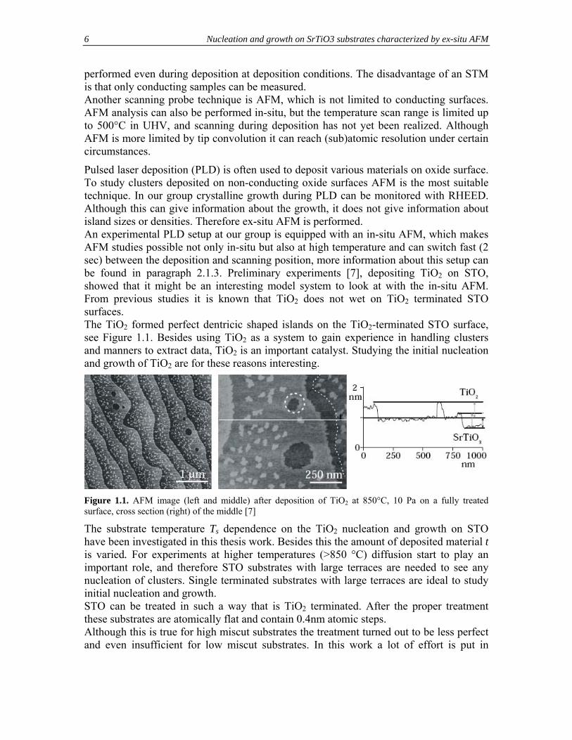
Pulsed laser deposition (PLD) is often used to deposit various materials on oxide surface. To study clusters deposited on non-conducting oxide surfaces AFM is the most suitable technique. In our group crystalline growth during PLD can be monitored with RHEED. Although this can give information about the growth, it does not give information about island sizes or densities. Therefore ex-situ AFM is performed. An experimental PLD setup at our group is equipped with an in-situ AFM, which makes AFM studies possible not only in-situ but also at high temperature and can switch fast (2 sec) between the deposition and scanning position, more information about this setup can be found in paragraph 2.1.3. Preliminary experiments [7], depositing TiO2 on STO, showed that it might be an interesting model system to look at with the in-situ AFM. From previous studies it is known that TiO2 does not wet on TiO2 terminated STO surfaces. The TiO2 formed perfect dentricic shaped islands on the TiO2-terminated STO surface, see Figure 1.1. Besides using TiO2 as a system to gain experience in handling clusters and manners to extract data, TiO2 is an important catalyst. Studying the initial nucleation and growth of TiO2 are for these reasons interesting.
Figure 1.1. AFM image (left and middle) after deposition of TiO2 at 850°C, 10 Pa on a fully treated surface, cross section (right) of the middle [7]
The substrate temperature Ts dependence on the TiO2 nucleation and growth on STO have been investigated in this thesis work. Besides this the amount of deposited material t is varied. For experiments at higher temperatures (>850 °C) diffusion start to play an important role, and therefore STO substrates with large terraces are needed to see any nucleation of clusters. Single terminated substrates with large terraces are ideal to study initial nucleation and growth. STO can be treated in such a way that is TiO2 terminated. After the proper treatment these substrates are atomically flat and contain 0.4nm atomic steps. Although this is true for high miscut substrates the treatment turned out to be less perfect and even insufficient for low miscut substrates. In this work a lot of effort is put in

1 Introduction 7
obtaining perfect low miscut STO substrates. Due to this fewer experiments have been performed on cluster deposition.
The rest of the report is divided as such: Chapter 2 will start with a theoretical background on the growth modes and the atomistic model used for describing nucleation and growth, paragraph 2.1. Next to that the analysis techniques to characterize the deposited TiO2 are presented. A special paragraph is devoted to the experimental setup that is being developed in our group, enabling quasi real-time in-situ AFM. For the experimental work performed with a pyrometer, the underlying theory is given in paragraph 2.2. The surface treatment for high miscut STO substrates is summarized in paragraph 2.3. Paragraph 2.4 summarizes properties of TiO2, techniques used to deposit TiO2 films and the different parameters influencing the phase of the resulting film. Chapter 3 gives on overview of the experimental work: substrate treatment, deposition method and the heater calibration experiments. Chapter 4 presents the results of the experiments. First dealing with the surface treatment, 4.1, accordingly the results for the heater calibration, 4.2, and finally the results for the nucleation and growth, or deposition experiments, 4.3. In the same order as in Chapter 4, the results are discussed in Chapter 5; notes will be placed at the results and suggestions for improvement will be given. Chapter 6 will summarize the conclusions made in previous chapters together with the suggestions for future research.
In the back of the report the Acknowledgements, the Appendices, a Symbol and a distribution list can be found.

Nucleation and growth on SrTiO3 substrates characterized by ex-situ AFM 8
2 Theoretical Background This chapter starts with describing the initial growth of crystals, 2.1, dealing with growth modes and the atomistic model, 2.1.1, and the techniques, RHEED and (quasi real-time) AFM, making visualization of these processes possible, 2.1.2 and 2.1.3. Paragraph 2.2 explains the theory behind radiation pyrometry. Information about the STO substrate treatment is summarized in paragraph 2.3. At the end of the chapter the TiO2 properties and techniques to deposit TiO2 are described, 2.4.
2.1 Nucleation and Growth of Clusters Since the dimensions of devices are shrinking constantly, approaching the nanometer scale, detailed knowledge of the fundamental growth processes is desirable. In paragraph 2.1.1 four crystal growth modes are introduced, describing the growth of thin films. Also the atomistic model describing the different processes responsible for the crystal growth is summarized. In order to understand these processes growth monitoring is important. With this information improving thin film properties is one step closer. In paragraph 2.1.2 and 2.1.3 the used monitoring techniques to measure these processes are described.
2.1.1 Crystal Growth In Figure 2.1 four generally accepted growth modes are depicted. Figure 2.1(a) is the layer-by-layer, or Frank-Van der Merwe, growth mode. This mode is observed when atoms are more strongly bound to the substrate than to each other. When there is no (strong) bonding between the substrate and the arriving particles, three dimensional island growth can be observed, Figure 2.1(b). The layer plus island growth, or Stranski-Krastanov, growth mode is an intermediate case. After the first or a few monolayers subsequent layer growth is unfavorable and islands are formed on top of this ‘intermediate’ layer. If the diffusion length, ld of adatoms is longer than the terrace width, lT, step flow growth mode is observed.
Figure 2.1. Film growth modes: layer-by-layer; Frank-Van der Merwe (a), island; Volmer-Weber (b), Stranski-Krastanov (c) and step flow (d) [4]

2 Theoretical Background 9
The growth modes are a thermodynamic approach to crystal growth, however in many vapor-phase depositions techniques, e.g. PLD, kinetic effects have to be considered. The individual atomic processes responsible for adsorption and crystal growth on the surface are illustrated in Figure 2.2. A source supplies single atoms (number density n1 (t)) on a substrate with N0 sites per unit area, making the single-atom concentration n1/N0. These atoms may then diffuse over the surface until they nucleate or re-evaporate. Atoms or clusters can be captured at (defect) sites such as steps or nucleate in new 2D or 3D clusters. Each of these processes will be governed by characteristic times, dependent on the single-atom concentration and/or coverage. If such processes are thermally activated, activation energies and frequency factors also play a role [8].
Figure 2.2. Schematic diagram of processes and characteristic energies in nucleation and growth on surfaces [8]
The nucleation density, Nx, of clusters is determined by the amount of particles arriving on the surface, R (deposition rate) and the distance an atom can travel on a flat surface, the diffusion length.
τ⋅= Sd Dl
Equation 1
τ is the residence time before re-evaporation or incorporation. DS is the diffusion coefficient defined as:
)exp(2
TkEaD
b
AS −=ν
Equation 2
EA being the activation energy for diffusion, ν the attempt frequency and the characteristic jump distance. From
aEquation 1 it is clear that the deposition temperature
(substrate temperature) is important, influencing the ld, and with that the nucleation density. Nucleation density experiments can therefore be used to extract EA. Rijnders used RHEED intensity, I, variations to extract EA [4]. RHEED intensity is coupled to the step density, S, which is related to the Nx and the coverage, θ(t). Summarizing:
),,()))(),,((( tTRItTRNSI x →θ

Nucleation and growth on SrTiO3 substrates characterized by ex-situ AFM 10
Although RHEED provides a growth fingerprint, the actual clusters can not be observed. To observe clusters, real space imaging like AFM, is needed. SPM measurements will not only give information about cluster densities, but also about cluster size distribution, lateral distribution, cluster heights, cluster shapes, and nucleation densities around special site (steps, defects). With this data besides EA more can be extracted. In literature various models are described to extract different activation energies from real space imaging data. A review by Venables et al. explains how real-space imaging provides data to test quantitative nucleation theories [8].
2.1.2 Atomic Force Microscopy AFM [9] is a real-space imaging method that enables one to characterize and manipulate surfaces, nanostructures and molecules at the nanometer length scale, and in some cases down to the atomic scale. Depending on the type of probe used, next to topography, other specimen characteristics can be mapped.. AFM can be performed in either Contact Mode (CM) or Tapping Mode (TM) [10,11]. Different AFM imaging modes rely on the interaction of a tip located at the end of a cantilever with the surface. This interaction influences the cantilever properties which can be detected with a motion sensor. A simplistic view of different AFM modes is displayed in Figure 2.3. A standard AFM image consists of a raster scan of n lines with on each line n measurement points. In constant force mode, the force applied by the tip on the sample is kept constant, this is done by adjusting the distance between the tip and sample surface in a feedback loop. This signal is also used to image the surface topography. In tapping mode the tip is oscillating in vertical direction at its resonance frequency. Tip–surface interactions will result in a change of the oscillation amplitude and resonance frequency. These signals or the adjustments of the tip-sample distance can again be used to image the surface.
In our group the Nanoscope IV (Di, Santa Barbara, CA), capable of contact and tapping mode imaging, is used. To measure the topography CM and TM has been used. Friction contrast has been used to check the STO surface termination.
Figure 2.3. Schematic representation of the different AFM imaging modes[12]
2.1.3 Quasi Real-time AFM During Pulsed Laser Deposition For more than a decade STM has been a powerful method to study surface structures down to the atomic level. Initially, STM snapshot images of a layer, grown at elevated temperature, were obtained at room temperature after the growth had been terminated. These studies already provided valuable information on the surface morphology of thin

2 Theoretical Background 11
films. However, these measurements are done after cooling the sample and exposure to the ambient, the influence of this is often unknown. Beside this in-situ and ex- situ measurements are time consuming and measuring the exact same surface as function of coverage is hardly possible. Voightländer demonstrated scanning with STM during MBE-deposition, which is quite an improvement [13].
A disadvantage of STM imaging is that it is limited to conducting surface and materials. To extend the number of materials that can be studied during deposition, AFM can be used. With AFM metal oxide surfaces, like STO, could be investigated for example. Metal oxides are often deposited by Pulsed Laser Deposition, see chapter 3.3. A PLD equipped with an in-situ AFM is under development in our group. Several major challenges have to be overcome in combining PLD with AFM: the presence of the plasma plume (I), operation at deposition conditions usually used for oxide pulsed laser deposition; temperatures between 20-750°C in a background gas of O2, Ar of N2 with a pressure ranging from 10-5-10-1 (II), and sufficient resolution to observe atomic steps and features at deposition conditions (III). To tackle these challenges the following requirements have been considered:
1. Prevent material deposition on the AFM-head parts like, piezo-elements, tip and cantilever (I)
2. Minimize heating of AFM-head parts, like piezo-elements and electrodes (II) 3. Minimize the lateral thermal drift coefficient between the tip and sample
(<100nm/K) (II) 4. Minimize thermal equilibrium time of the heater-sample-AFM configuration
(<90min at 700ºC ) (II) 5. Measure in different gas environments(like: O2, N2, Ar) and pressures (10-6-
103mbar) (II) 6. Vibration isolation for AFM and RHEED (III)
Combining AFM and PLD is not straightforward because both occupy the same space. To cope with this challenge (1), the position for deposition and AFM imaging is separated. The sample is kept at deposition conditions during transfer from one to the other position. In this way there is no shielding effect of the AFM, blocking material in the plume. To make snapshots of the surface in between pulses high speed AFM (one frame per second) has to be implemented. This is particularly interesting if the transfer- and approach mechanism is fast. High speed AFM is being developed by others and we expect it to be available soon. A fast transfer- & approach is realized with a new approach mechanism called “the side approach” (European patent
1
2
35
4
6
7
9
5
38
10
1111
1
2
35
4
6
7
9
1
2
35
4
6
7
9
5
38
10
11
5
38
10
1111
Figure 2.4. Schematic representation of the PLD/in-situ AFM setup; alumina frame with on it the AFM, target and sample. 1: Clamping mechanism (1) 2: AFM 3: Sample holder slide Part 4:Attocube Part 5: Target 6: Steppermotor 7: Adjustment spring,8 plasma plume, 9 alumina frame, 10 Laser beam, 11 alumina plate

Nucleation and growth on SrTiO3 substrates characterized by ex-situ AFM 12
nr. 06076925.4). It takes about 2 seconds to start scanning again after a deposition pulse with a separation between deposition and AFM position of 60 mm. Fast approaching is done by approaching only ones; by putting the sample surface under a small angle the movement between the deposition and AFM position can be used to retract and approach. With this setup quasi real-time imaging of the surface after a deposition pulse can be realized.
To measure samples at temperatures above 500 °C the piezo-scanner in the AFM head is thermally shielded from the hot sample surface, challenge 2. To minimize the thermal mass of the heating stage a low thermal mass heating stage has been developed in our group. The low thermal mass and the shielding minimize the thermal drift, challenge 3, and the thermal response time, challenge 4. Calibration of these low thermal mass heaters can be found in paragraph 4.2.2.
Challenge 5, measuring in different gases, was proven to be possible, simply by doing so. Challenge 6, vibration isolation is done in several ways. The vacuum chamber and turbo pump are separated by a flexible connection and electrical and optical cables are fed out through the AFM-PLD support-tube. To reduce noise even further the cables of the AFM, motors and heater are fixed to the AFM-PLD support and stepper motors are switched off during measurement. Teflon coated UHV sliders with dovetail connection on which AFM and sample stage are mounted are used to damp external vibrations. Passive damping is used by placing the total vacuum system on four air-damped pods. Additionally the stiff AFM-PLD support tube mounted in the vacuum chamber is actively damped.
The performance of the hotstage is obtained by minimizing the heat loss through conduction. This loss is limited by hanging the heated filament (2x2x1 mm3) almost freely in air or vacuum instead of using some other insulating material. On top of the heated stage (4x2x1 mm3) a (non)conducting sample 2x2xh mm3 can be mounted. Compared to direct current heating this heater can support any kind of substrate in different environments form UHV to ambient. Besides a small thermal mass the heater configuration is mechanical and chemical stable and convenient for sample mounting. The temperature of the heater is calibrated in the following chapters. Up to 800ºC in 10-2
mbar O2 and till 500 °C in ambient scanning with atomic step resolution has been realized.
2.2 Radiation Pyrometry To scan at elevated temperatures with the in situ AFM small thermal heaters have been developed and tested. Since TiO2 is a model system for the in-situ AFM and the formation of nano-islands is temperature depended accurate temperature calibration is required.
All substances at temperatures above absolute zero emit radiant energy as the result of the atomic and molecular agitation that is associated with the temperature of the substance [14]. The rate of emission per unit area increases with increasing temperature. The radiant energy is distributed over the wavelengths it radiates.
A radiation pyrometer can be used to determine the temperature of an object. The blackbody is a theoretical object, which is a complete absorber. This means that it absorbs all the energy that incident upon it. Therefore all the energy this object emits, W, is

2 Theoretical Background 13
determined by the temperature of the object. It is a perfect radiator. A substance that does not absorb all the radiation that falls upon it from an external source radiates its own energy at a rate less that the rate of emission of a blackbody at the same temperature. This is known as a non-blackbody. Such an object partly reflects (R) the incoming energy and partly passes entirely through (T) (for non-opaque non-blackbodies). Summarizing:
− Blackbody: R=0; T=0 − Opaque non-blackbody: T=0 − Non-opaque non-blackbody: -
The radiation emitted by a non-blackbody may be expressed as a fraction of the radiation that would be emitted by an otherwise comparable blackbody at the same temperature. This fraction is termed the emittance or emissivity, ε, of the non-blackbody. The radiant energy of the object can be described by the Stefan-Boltzmann law: Blackbody:
4TW ⋅= σ Non-blackbody:
4TW ⋅⋅= σε with ε between 0 and 1. If the emissivity of an object under investigation is know, the energy it radiates can be used to determine the temperature of the object. To calibrate the low power heaters a Heat Spy DHS54 (Palmer Wahl, Cincinnati, OH) was used, an instruments that determines the temperature with the principle described above.
2.3 The Surface Treatment of SrTiO3 STO has a ABO3 perovskite structure, having either A (SrO) or B (TiO2) terminating planes in the (001) direction, see Figure 2.5. A material wets B, and B material wet A planes, but A on A or B on B has a non-wetting behavior resulting in island growth [7,15]. TiO2 in the anatase phase is expected to grow epitaxial on STO due to the small lattice mismatch. As-received STO(001) substrates are flat, but far from perfect. Due to the substrate cutting and mechanical polishing processes afterwards the atomic steps on the surface are hardly visible and the surface is double terminated. By annealing an as-received STO(001) substrate, large terraces can form with the average width determined only by the miscut angle. However, it typically has both SrO-terminated and TiO2-terminated terraces with more or less equal proportions. A SrO-terminated terrace is chemically different from a TiO2-terminated terrace, therefore selective chemical etching can be used to remove the AO plane.

Nucleation and growth on SrTiO3 substrates characterized by ex-situ AFM 14
Kawasaki et al. proposed a chemical route to TiO2-single terminated STO [16]. They used a Buffered NH4F-HF (BHF) solution with pH=4.5. They immersed the STO in the BHF solution for 10 min, rinsed them with pure water and ethanol, and dried them in a nitrogen stream. In a later publication, Kawasaki et al. added an annealing step around 600°C in Ultra High Vacuum to obtain a well-defined STO surface [17]. Kawasaki et al. procedure is based on the selective etching of the more basic oxide SrO and thus the pH value of the solution is claimed to be crucial. Koster et al. however found the reproducibility to be severely dependent on the different polishing and annealing procedures prior to the BHF treatment [18]. This often leads to uncontrolled etching and introduced unit cell deep holes in the terraces and deep etchpits. They improved the procedure by separating the main reaction step, hydroxylation of SrO by immersion in water, and the dissolving in BHF. Due to the enhancement of the selectivity in solubility by the formation of a Sr-hydroxide complex, confined to the topmost SrO layer, the pH value of the BHF solution and etch time become less critical. The current procedure consists of ultrasonically soaking an as-received substrate in analytical grade and demineralized water for 10 min, followed by a short (~30 s.) dip in standard, commercially available BHF solution for the etching [18,15]. In another writing Koster et al. report that the etching results in smoother terraces if performed ultrasonically [19]. To remove remnants of the previous treatments and facilitate recrystallization, a final annealing step is performed at 950 °C for 1 hr. Fei et al. report that they also obtained nearly perfect TiO2-terminated STO(001) by using a combination of chemical etching and thermal annealing, as suggested by Koster et al [20].
Figure 2.5. ABO3 crystal structure and possible terminating planes of a (001) surface
STO substrates can also be SrO-terminated, e.g. using Molecular Beam Epitaxy (MBE) [16], PLD [21], reactive ion etching [22]. No such experiments are in this thesis.
2.4 Titanium Dioxide, TiO2 Titanium dioxide, TiO2, is the most investigated single-crystalline system in the surface science of metal oxides [13]. TiO2 is applied in heterogeneous catalysis, as a photocatalyst, in solar cells for the production of hydrogen and electric energy, as gas sensor, as white pigment, as a corrosion-protective coating, as an optical coating, in ceramics, and in electrical devices such as varistors.
TiO2 crystallizes in three major different structures: rutile (tetragonal, a = b = 4.584 Å, c = 2.953 Å), anatase (tetragonal, a = b = 3.782 Å, c = 9.502 Å) and brookite (rhombohedrical, a = 5.436 Å, b = 9.166 Å, c= 5.135 Å) [13]. Rutile is the most stable phase. Anatase is metastable, and is only synthesized at relatively low temperatures. Brookite is formed only in extreme conditions. However, only rutile and anatase play any

2 Theoretical Background 15
role in the applications of TiO2. For photocatalytic applications the anatase phase exhibits better activity than rutile. The Chemical Vapor Transport (CVT) is frequently used for preparation of anatase [23]. Crystallization of the amorphous titanium oxide synthesized by the hydrolysis method also results in the anatase phase [24,25]. More recently epitaxial anatase films were prepared by dissolving perovskite (CaTiO3, STO, and BaTiO3) in an aqueous environment; the substrate being the source of the film material [26]. Chemical vapor deposition has also been used to grow epitaxial TiO2 films, Blanton et al. showed depending on the substrate used, they could either grow rutile of anatase films [27].
Pulsed laser deposition can also be used to grow thin films of TiO2. Which phase forms depends on the deposition conditions. Kitazawa et al. report on the formation of TiO2 thin films (>200 nm) using a α-Al2O3 substrate and a Ti-target. Depending on the substrate temperature and the pressure of the O2 gas either anatase or rutile films are formed (anatase at high pressure, 80 Pa, and high temperature, 500 °C) [28,29]. The laser repetition rate also influenced which phase was formed. Where anatase films (1.4 μm) are formed at any frequency at 150 °C (substrate temperature) on a Si(110) substrate, it forms rutile at higher frequencies when the experiment is performed at 300 °C, according to Inoue et al. [30]. Also laser energy, influencing the excitation temperature of the plasma [31], and the distance between target and substrate [32] can play a role weather one phase or another is formed. The phase of the growing film can also be determined by the crystal structure of the substrate. As mentioned above, on α-Al2O3 both rutile and anatase films can be grown, depending on the settings of the deposition. On Si(100) and Si(111) substrates different settings also result in the growth of either anatase or rutile, even brookite is observed [33,31,32]. The underlying layer, where the TiO2 is deposited on can also influence the catalytic activity as is demonstrated by Frey et al. [34].
For epitaxial growth, the lattice parameters of the substrate should more or less match the lattice parameters of the, desired, anatase phase. LaAlO3 (001) would be a good candidate having a lattice mismatch of -0.2 % with anatase. Articles describing the growth of the anatase phase thin films (50 – 2500 nm) on LaAlO3 using PLD or (laser) MBE [35,36,37] can be found. In these articles LaAlO3 is often compared with STO, having a lattice mismatch of -3.1 %, another suitable substrate for growing anatase films. Due to the induced strain by the higher lattice mismatch, anatase films grown on STO are often of lower quality, but this increases with increasing film thickness. [36] Hsieh et al. report that TiO2 films were found in the anatase phase over a wide range of deposition parameters; a temperature range of 200-1000 °C and PO2 ranging from 5·10-6 to 0.1 Torr (1 Torr = 1.33mbar) [38]. Rutile films were made by deposition of a TiN layer, which was subsequently oxidized.
Summarizing, thin films of TiO2 can be prepared using different techniques. One of these techniques suitable for this is PLD. Also post-deposition treatments like annealing can determine the final phase of the thin layer. To form anatase TiO2 on STO is a suitable substrate and PLD can be used.
Articles in literature use terms like nanocluster and nanoparticles, to describe the morphology of the upper layer of the thin film. These layers are usually 50 up to 2500 nm

Nucleation and growth on SrTiO3 substrates characterized by ex-situ AFM 16
thick. In this thesis however we want to look at independent nanocluster or islands, which means that we will deposit less than one monolayer, non-closed monolayers.

3 Experimental In this Chapter the experimental equipment and performed procedures are described. Paragraph 3.1 deals with the substrate cutting followed by the substrate treatment in 3.2 . The pulsed laser deposition principles, setup and experimental work is outlined in 3.3. Paragraph 3.4 deals with the AFM and heater calibration experiments.
3.1 Substrate Cutting As-received substrates were either 10x10x1 mm3, or 5x5x1 mm3. The substrates are cut in to smaller, but still manageable, 2x2x1 mm3 pieces, from now on referred to as 2x2 substrates. To prevent the pieces from turning over in the storebox, silica gel and double-sided-tape was used. The silica gel works, but double-side-tape was the best solution to store these small samples safely.
The cutting procedure: A piece of glass is heated on a plate till around 200 °C; resin is placed on the heated glass to melt it. The substrate is, polished side down, placed in the melted resin, after which it is cooled and aligned in the cutting machine (11-1180 low speed saw, Buehler Ltd, Illinois, USA). After aligning the substrate, it is cut using a, water cooled, diamond saw. After being cut, the resin is heated again to remove the 2x2 substrate pieces. They are subsequently placed in several Acetone baths and are ultrasonically treated in a Branson 2200 (Branson, Connecticut, USA) for at least 10 minutes to remove the resin. This is repeated for another 5 minutes in a new Acetone bath and finally 10 minutes in ethanol. After this the substrates are blown dry with N2-gas. Before further use, they are checked with an optical microscope and further cleaned if necessary.
3.2 Etching and Annealing of Substrates Etching of the substrates is necessary to obtain single-terminated STO surfaces. Since the HF-buffer is dangerous direct contact with the skin and or eyes has to be prevented. Therefore these experiments are performed with a special lab coat, special gloves and glasses.
The etch process: The substrates are placed on a substrate holder and ultrasonically soaked* in Demi-water for at least 20 minutes. After this water treatment the substrates are placed on another substrate holder†. The substrates are subsequently ultrasonically treated with a commercially available buffer HF solution (BHF. MERCK) for x seconds. Coming chapters will show that the treatment is not as successful for low miscut substrates as for high miscut substrates. To optimize low miscut STO surfaces, experiments are done varying x between 30‡ and 120 seconds. After the BHF treatment the substrates are four times rinsed with water and once with ethanol to facilitate the drying with N2-gas.
Annealing: * All cubs used for experiments are made from plastic instead of glass, to prevent any damage to the substrates. † See discussion for this step in the treatment ‡ 30 seconds is the length of etching found to be adequate in literature

Nucleation and growth on SrTiO3 substrates characterized by ex-situ AFM 18
To obtain the desired crystalline perfection of the substrate surface a heat treatment at 900-950 °C is performed. Since the overall etch and anneal treatment turned out to be insufficient for low miscut substrates the annealing time is varied between 1 and several hours. The heating is done in a tube oven, which reaches 950 °C in less than 30 minutes and cools down in about 2 hr with an oxygen flow of 200 ml/min. Annealing times mentioned in this thesis are exclusive the 30 minutes to reach the annealing temperature and the cooling down to room temperature.
Due to unexpected results of the surface treatment experiments have been done to determine the mechanism behind the treatment in order to optimize it. For this reason the hydrolysis, the etching and the annealing step have been investigated.
3.3 Pulsed Laser Deposition Pulsed Laser Deposition (PLD) [39] is used to deposit thin films, but is also suitable for sub-monolayer deposition. PLD has several advantages such as the possibility to deposit virtually any material, from pure elements to compounds. PLD is a simple and flexible technique in which many deposition conditions can be varied like, temperature, gas atmosphere, fluency, laser repetition rate etc.
3.3.1 Principles In PLD a highly energetic laser beam is focused on a target using lenses. This laser ablates the target creating a dense layer of vapor in front of the target. In the remaining duration of the laser pulse the energy is absorpted by this layer Expansion of this vapor forms the so-called ‘plasma-plume’. If a substrate is place in or near to the plume, part of the ablated material will condensate and form a thin film. The kinetic energy of the particles arriving at the substrate is determined by the background gas, the fluency, the repetition rate and the pulse duration.
Figure 3.1. Picture of the Pulsed laser Deposition system with RHEED monitoring at the Thin Film Laboratory (Twente University, The Netherlands)

3 Experimental 19
3.3.2 Setup All depositions described in this thesis were done at the Thin Film Laboratory with PLD, see Figure 3.1, using a KrF excimer laser (λ=248m) (Lambda Physic LPX 210 , Göttingen, Germany). The laser has a maximum pulse energy of 1000 mJ, a pulse width of 25ns and a repetition rate between 0 and 100Hz. In Figure 3.2 we see a schematic picture of the deposition chamber. In the chamber is a target holder, which can hold up to 5 targets. In front of the target holder is the heater, on which the substrate can be mounted. The deposition chamber is pressurized using a turbo-molecular drag pump. For background gas, there is an inlet for Ar and O2 and the pressure range is 1x10⁻⁶mbar. This setup is also equipped with high-pressure RHEED.
Figure 3.2. schematic view of the pulsed laser deposition process/setup
3.3.3 Depositions in the PLD-RHEED System In this section TiO2 deposition settings are given, see Table 3-1. Also the substrate handling steps are briefly given for loading and unloading in the PLD system.
Parameter value Pback ~10-7 mbar Pdeposition 1.3 10-1 mbar O2- flow 28 mbar·l/min Tdeposition 750-900 °C Repetition rate 0.25 Hz Target TiO2Pulses 5-320 spotsize 2.15 mm2
Steps involved in performing a deposition: Before gluing the sample to the heater, it has to be cleaned, to remove any residues from previous depositions. This is done with sandpaper and a subsequent cleaning step with ethanol. The substrate is accordingly glued at the centre of the heater using a silver-paste. The heater is heated, ~150 °C, to remove the solvents from the silver-paste. Table 3-1. Deposition Parameters used for the
deposition of TiO2 on STO (001)

Nucleation and growth on SrTiO3 substrates characterized by ex-situ AFM 20
The heater is loaded on the loading-stick in the loadlock chamber, from now on referred to as loadlock, which is at atmospheric pressure during loading. Next the loadlock is pressurized to match the pressure in the deposition chamber. The heater can now be loaded onto the heater holder, equipped with a thermocouple. At this point the pressure is ~10-7 mbar, Pback. The oxygen flow is set at 28 ml/min, and the pressure in the chamber is set at 1.3·10-1 mbar (13 Pa). The heater is set at the desired temperature (700 – 900 °C). During heating, the laser, the mask and target are aligned and laser energy is set at 28 mJ behind the mask (2x15 mm mask), which equals 1.3 J/cm2 on the target. The target is scanning from left to right over 4 mm distance, and is pre-ablated at 5 Hz. Once the heater has reached its temperature, the RHEED can be aligned, See Figure 3.3.
Figure 3.3. A typical RHEED. The spot below is the unreflected RHEED bundle. The other spots are from the substrate
3.4 Heater Calibration The resistance of the low thermal mass heaters (≈0.8 Ω/K) can act as a temperature sensor. However, we want to check if the heaters calibrated resistance versus temperature data is correct and compare them with other SPM hot stages.
To determine several characteristics of the low power heaters a thermocouple or a pyrometer can be used. However with a thermocouple a good thermal contact is necessary especially in vacuum. This contact would act as a heat sink and influence the temperature. Besides this a thermocouple would influence the required power drastically. To compare these heaters with others used in the SPM-field the power versus temperature curves is necessary. For these reasons not a thermocouple but a non-contact pyrometer, Heat Spy DHS54 (Palmer Wahl, Cincinnati, OH), is used. The Heat Spy has a temperature range of 500 to 3200 °C and is focused on the 2x2 mm substrates mounted on the heater.
During the experiments the voltage across and the current through the heater resistance was measured to calculate the resistance and power. Besides this the pyrometer is used to record the temperature. However measurement errors with a pyrometer occur due to an uncertainty and errors of the surface emissivity. To calibrate the temperature of this substrate surface the emissivity of the chemical ant thermal treated STO is required. Literature reports emissivity values for treated STO ranging from 0.8-0.3 [40,41]. Therefore experiments have been performed to determine the emissivity of treated STO.
4 Results This chapter can be divided in three main paragraphs: the surface treatment, 4.1, the heater calibration, 4.2, and the nucleation and growth of TiO2, 4.3. In Chapter 5 the presented results will be discussed.
This paragraph contains many AFM images. For sake of overview, most of them can be found in Appendix B. If one is directed to an image, it can be found in the appendix, sometimes the image is also displayed in the chapter. In the Appendix underneath the images dimensions of the image and a summary of the treatment of the substrate till the point of imaging are given. The height bars of these images are for topography images 1.5-2 nm and for friction images 500 mV.
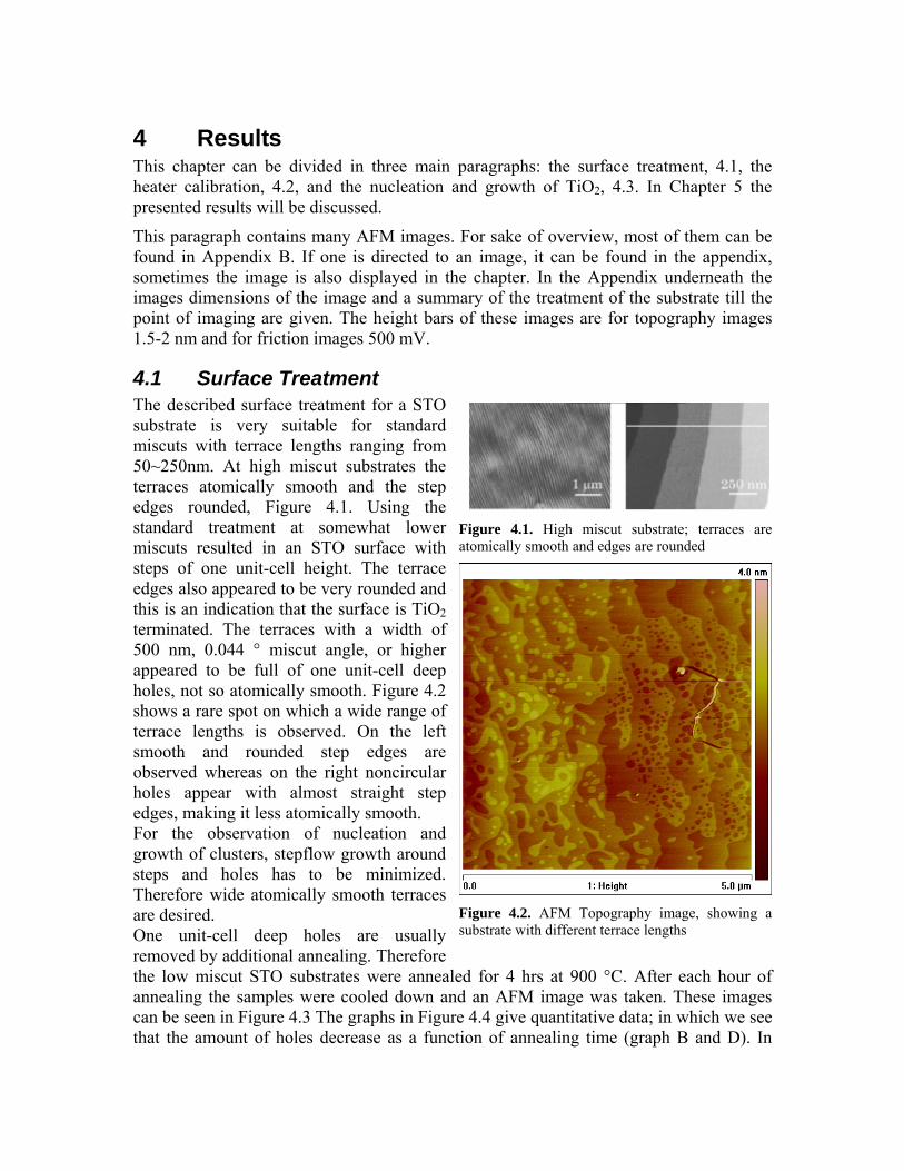
4.1 Surface Treatment The described surface treatment for a STO substrate is very suitable for standard miscuts with terrace lengths ranging from 50~250nm. At high miscut substrates the terraces atomically smooth and the step edges rounded, Figure 4.1. Using the standard treatment at somewhat lower miscuts resulted in an STO surface with steps of one unit-cell height. The terrace edges also appeared to be very rounded and this is an indication that the surface is TiO2 terminated. The terraces with a width of 500 nm, 0.044 ° miscut angle, or higher appeared to be full of one unit-cell deep holes, not so atomically smooth. Figure 4.2 shows a rare spot on which a wide range of terrace lengths is observed. On the left smooth and rounded step edges are observed whereas on the right noncircular holes appear with almost straight step edges, making it less atomically smooth.
Figure 4.1. High miscut substrate; terraces are atomically smooth and edges are rounded
For the observation of nucleation and growth of clusters, stepflow growth around steps and holes has to be minimized. Therefore wide atomically smooth terraces are desired.
One unit-cell deep holes are usually removed by additional annealing. Therefore the low miscut STO substrates were annealed for 4 hrs at 900 °C. After each hour of annealing the samples were cooled down and an AFM image was taken. These images can be seen in Figure 4.3 The graphs in Figure 4.4 give quantitative data; in which we see that the amount of holes decrease as a function of annealing time (graph B and D). In
Figure 4.2. AFM Topography image, showing a substrate with different terrace lengths

Nucleation and growth on SrTiO3 substrates characterized by ex-situ AFM 22
graph A an increasing distance between a step-up and the holes is observed, the holes seem to move toward the step edge. The mean area of the holes stays constant, graph C; the exception is after 4 hours annealing, but that can be subscribed to the low amount of holes detected. This would mean that the holes move toward a step down and do not merge with each other during the diffusion process. Annealing the substrate at 900 °C seems to be a suitable treatment to remove the holes from the terraces, the movement of the holes is contributed to diffusion, they diffuse to the edge of the terrace on step down [7]. Merging of the holes might be happening, but is not favorable, since no increase of the holes is observed.
Figure 4.3. AFM topography images having 3x3 micron dimensions. A after 1 hr, B after 2 hrs, C after 3 hrs, D after 4 hrs annealing at 900 °C
Figure 4.4. Graphs with data extracted from Figure4.2. a) Dependency of diffusion length, b) holes density, c) average size of holes and d) coverage of holes on annealing time at 900 °C
To study the TiO2 nucleation as a function of coverage it is important to have similar starting surfaces. The surface treatment experiments were performed with substrates (5x5 mm2) cut from the same main substrate (10x10 mm2). Since they were treated simultaneously and variations during the treatment are minimal, the same results are expected for each substrate. However, as can be seen from Figure 4.5 this is not the case.
4 Results 23
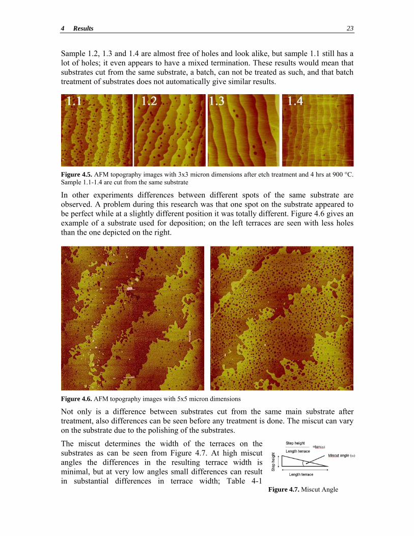
Sample 1.2, 1.3 and 1.4 are almost free of holes and look alike, but sample 1.1 still has a lot of holes; it even appears to have a mixed termination. These results would mean that substrates cut from the same substrate, a batch, can not be treated as such, and that batch treatment of substrates does not automatically give similar results.
Figure 4.5. AFM topography images with 3x3 micron dimensions after etch treatment and 4 hrs at 900 °C. Sample 1.1-1.4 are cut from the same substrate
In other experiments differences between different spots of the same substrate are observed. A problem during this research was that one spot on the substrate appeared to be perfect while at a slightly different position it was totally different. Figure 4.6 gives an example of a substrate used for deposition; on the left terraces are seen with less holes than the one depicted on the right.
Figure 4.6. AFM topography images with 5x5 micron dimensions
Not only is a difference between substrates cut from the same main substrate after treatment, also differences can be seen before any treatment is done. The miscut can vary on the substrate due to the polishing of the substrates.
The miscut determines the width of the terraces on the substrates as can be seen from Figure 4.7. At high miscut angles the differences in the resulting terrace width is minimal, but at very low angles small differences can result in substantial differences in terrace width; Table 4-1
Figure 4.7. Miscut Angle

Nucleation and growth on SrTiO3 substrates characterized by ex-situ AFM 24
illustrates this. Sample 1.1 and 1.4, are cut from the same main substrate just as sample 10 and 17.
terrace width
(nm) miscut angle
(°) Sample 1.1 500 0,045 Sample 1.4 300 0,075 Sample 10 ~ 500 0,045 Sample 17 > 2000 0,011
Table 4-1. Effect of miscut angle on terrace width
For our experiments the large terraces (>500 nm) provide room for nucleation and formation of clusters. For experiments at high temperatures, >850 °C, wide terraces are desired, as will be explained in paragraph 4.3 Next to that, substrates are bought in a miscut range, and also therefore proper treatment of substrates with wider than 500 nm terraces, miscut angle < 0.044°, is desired. Step by step the procedure is changed, in order to find the optimal treatment for low miscut substrates.
The experiments to obtain single terminated STO with large terraces will be shown below. The order in which they are presented is more or less also the order in which they were performed.
4.1.1 30 Seconds Etching, Annealing at 900 °C The initial treatment resulted in images as depicted in Appendix B A-H, for substrates with <500 nm terrace width this results in single-terminated substrates. Although, above there was already some doubt about the quality of the substrates, Figure 4.5-1.1. J and K, close-ups from Figure 4.6, not only illustrated a surface difference between slightly different positions, but also the abundance of holes on low miscut substrates treated with the standard procedure. L, Figure 4.8 also illustrates this abundance; it is almost completely covered with holes. These holes did not get out at all after hours and hours of annealing. It was already mentioned that batch treatment does not necessarily guarantees the same results. This is strengthened by the observations in M, N. These 2 samples are treated simultaneously. Another problem in comparing results is that we are unable to image the same area before and after treatment. This in combination with the observed differences between spots on a substrate makes drawing conclusions after initial growth observations and surface treatments difficult. O, P illustrate sample 33 before and after a heat treatment at 900 °C. Two complete different pictures arise, if this is due to the heat treatment, or the difference between the spots imaged cannot be determined.
In M and O for the first time straight eedges and holes arise on the images. These straight edges Figure 4.8. AFM topography image. L: sample 17,
5x5 micron

4 Results 25
are associated with a double termination. Also part of the holes of O are more than one unit cell deep, and at every step ledge there is a deep hole, etch pit observed. These can be up to 1 nm, see Figure 4.9.
Figure 4.9. AFM topography image. Substrate after 30 sec etching and 1hr annealing at 900 °C. Right a cross-section is given, observed is an etchpit at the ledge.
4.1.2 Changing the Annealing Temperature, 900 950 °C Because of unexpected results, the treatment was changed to an annealing step at 950 °C, instead of 900 °C. This temperature is usually used to obtain the desired crystalline perfection of the substrate surface [4]. In Q-β some results are displayed, with S, U, W, Y and α being the AFM friction images of R, T, V, X and Z respectively. All the images show a double terminated surface. This can be seen on the friction images and the straight step edges. In image β the surface of a substrate is shown, which was annealed for 12 hrs after a 30 second etch treatment. The height differences seen in this image are ½ unit cell, making it an almost 50:50 ration of SrO:TiO2 at the surface. Increasing the temperature to 950 °C has resulted in fewer holes in the terraces, but also seems to result in a mixed surface termination. To find out whether the exposure of the substrate to air between the hydrolysis and etch step has any influence on the appearance of mixed terminated surfaces, one experiment was done. One sample (X, Y) was kept in water in between the steps and the other (Z, α) was blown dry. The result of the one kept in the water, is a result never seen before. It seems like the surface is divided into domains although height differences between domains cannot be observed. Besides this friction contrast indicates that the surface is double terminated. This is probably a bad substrate. However XRD measurements do not provide evidence for this. The sample blown dry has terraces widths of 1000 nm which are almost free of holes and is slightly double terminated. The double termination and the strange results can not be explained by the dry surfaces just before etching.

Nucleation and growth on SrTiO3 substrates characterized by ex-situ AFM 26
Also there was looked at the pH of the BHF, which was determined to be pH=~4.5. This pH is in accordance with values found in literature.
4.1.3 Increasing Etch Time; 60, 90, 120 sec The AFM images γ−ς are the substrates etched for either 60, 90 or 120 seconds and annealed at 950 °C for 2 hours. For 60 seconds etching, compared to 30 seconds, an increased mixed termination can be seen in γ, η and ν. The surprising result of ν is that before annealing the surface seems to be single terminated. Single terminated surfaces seem to be obtained in ε, ι, λ and ξ. For ε and ι this might be attributed to the high miscut angle. This would mean that for low miscut angle substrates 60 as well as 30 seconds etching might be used, with the risk that with 60 seconds etch pits might emerge, see ε. For λ and ξ there can be noticed that they were both etched for the first time, while others were etched before. The results of the 90 seconds etching experiments are shown in ο to ρ. The terraces look single terminated, but straight ledges dominate the image. Image π and ρ are from the same substrate but taken at a different spot on the substrate, one showing one unit-cell high islands the other one unit-cell deep holes. One extreme low miscut angle substrate was etched for 120 seconds, ς. Holes dominate the surface, but at the same time large areas are available for deposition. These areas are single terminated. Notice that there are no etch pits observed, although the etch time is 120 seconds. Therefore etching does not seem the origin of the etchpits.
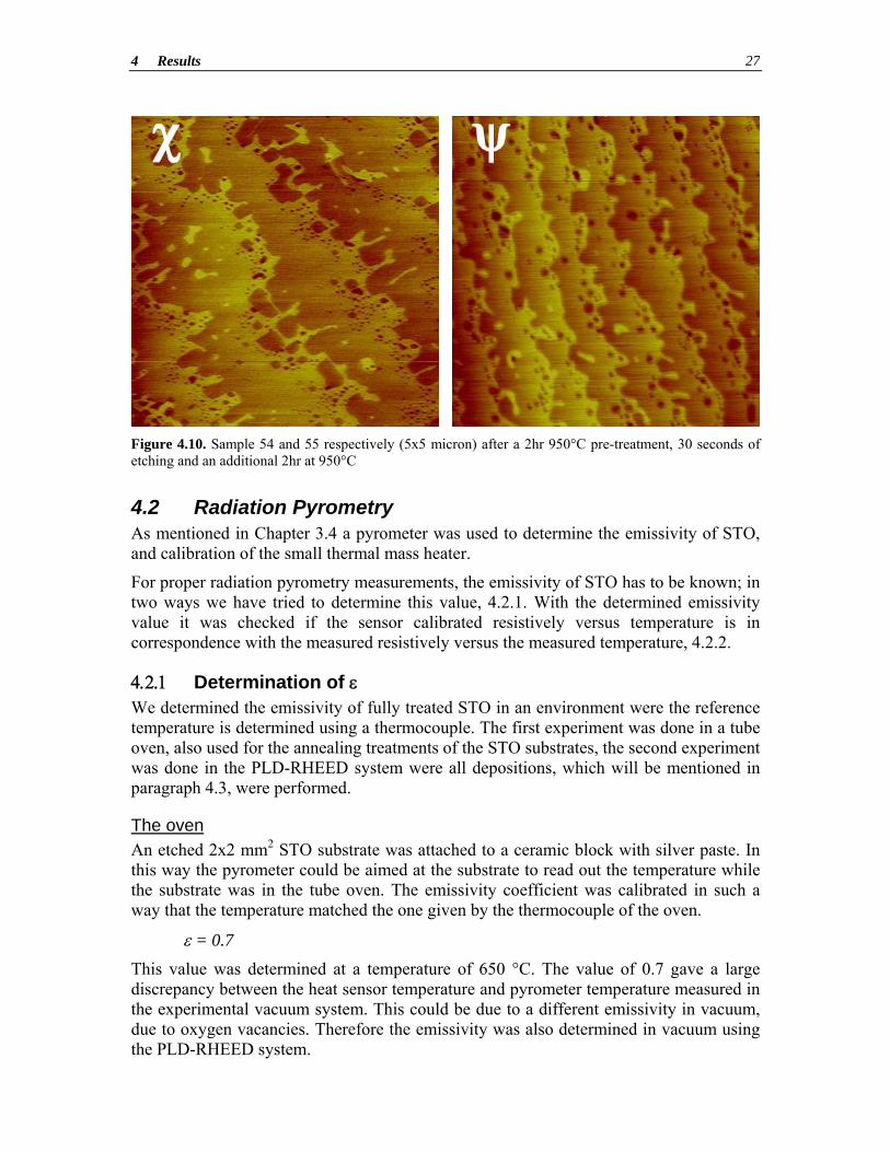
4.1.4 Pre-annealing Finally the process was changed by adding an additional step to the treatment. Before ultrasonically soaking the substrates they were annealed for 2 hours at 950 °C, giving the surface the opportunity to arrange itself. Hopefully separating the TiO2, and SrO terminating areas and decrease the amount of local defects. This step could improve the etch process. For one sample all the in between AFM images are shown, σ−φ. For 2 others the resulting surfaces are shown below, χ−ψ. As can be seen the holes in the low miscut substrate are all located close to the step edge. The terrace lengths range from 500nm to 2000nm. The lengths are large than 500nm and therefore suitable for deposition. The samples χ and ψ were not treated simultaneously with φ and also originate from another batch of substrates, indicating that this process gives reproducible results, unlike previous treatments.
4 Results 27
Figure 4.10. Sample 54 and 55 respectively (5x5 micron) after a 2hr 950°C pre-treatment, 30 seconds of etching and an additional 2hr at 950°C
4.2 Radiation Pyrometry As mentioned in Chapter 3.4 a pyrometer was used to determine the emissivity of STO, and calibration of the small thermal mass heater.
For proper radiation pyrometry measurements, the emissivity of STO has to be known; in two ways we have tried to determine this value, 4.2.1. With the determined emissivity value it was checked if the sensor calibrated resistively versus temperature is in correspondence with the measured resistively versus the measured temperature, 4.2.2.
4.2.1 Determination of ε We determined the emissivity of fully treated STO in an environment were the reference temperature is determined using a thermocouple. The first experiment was done in a tube oven, also used for the annealing treatments of the STO substrates, the second experiment was done in the PLD-RHEED system were all depositions, which will be mentioned in paragraph 4.3, were performed.
The oven An etched 2x2 mm2 STO substrate was attached to a ceramic block with silver paste. In this way the pyrometer could be aimed at the substrate to read out the temperature while the substrate was in the tube oven. The emissivity coefficient was calibrated in such a way that the temperature matched the one given by the thermocouple of the oven.
ε = 0.7 This value was determined at a temperature of 650 °C. The value of 0.7 gave a large discrepancy between the heat sensor temperature and pyrometer temperature measured in the experimental vacuum system. This could be due to a different emissivity in vacuum, due to oxygen vacancies. Therefore the emissivity was also determined in vacuum using the PLD-RHEED system.

Nucleation and growth on SrTiO3 substrates characterized by ex-situ AFM 28
PLD-RHEED system The same 2x2 mm STO substrate was pasted to the heater with silver paste and placed in the system. The heater was heated to 650 °C, using a thermocouple:
ε = 0.35 An emissivity of 0.35 was determined. Previous vacuum experiments in this system led to an emissivity of 0.3. This was caused be the fact that transmission loss through the window was not taken into account (~20 °C). Determining the emissivity appeared to be easy, but turned out to be quite complex.
4.2.2 Heater Calibration Temperature vs. resistance and temperature vs. power experiments were performed in the PLD-in-situ AFM setup. An STO substrate was pasted on the heater with silver paste and placed and wired in the system. The heat spy was used to determine the temperature (ε = 0.3) through a window in the system (transmission loss ~9 °C). At different pressures temperature vs. resistance and power were made. Resistance and power were determined by calculations with V and I. In the curves the 9 °C window loss are not taken into account.
VIWIVR == ,
R = resistance, V = potential, I = current
To verify that the sensor calibrated resistively versus temperature is in correspondence with the measured resistively versus the measured temperature both curves are given in Figure 4.11. Besides measurement points from 500 to 1000º the resistance (218Ω ±2) at room temperature is determined before and after a heat treatment. As can be seen the measured and calculated curves have the same slope in the temperature 500 to 800ºC range. The measured resistances at room temperature of both graphs are identical. If we extrapolate the measured data it can be concluded that the offset occurs due to a measurement error in the emissivity. Errors in the resistance read-out could have been introduced by severe connection wire heating. However the resistance versus temperature slope is as expected so this is not the case.

4 Results 29
0 200 400 600 800 1000
200
400
600
800
R293K
Rpyrometer
RPt-200
Res
ista
nce
[ohm
]
Temperature [ºC]
550 600 650 700 750 800 850
0.8
1.0
1.2
1.4
1.6
Pow
er[W
]
Temperature [degC]
10-1mbar 10-2mbar 10-3mbar
0 200 400 600 800 1000
200
400
600
800
R293K
Rpyrometer
RPt-200
Res
ista
nce
[ohm
]
Temperature [ºC]
550 600 650 700 750 800 850
0.8
1.0
1.2
1.4
1.6
Pow
er[W
]
Temperature [degC]
10-1mbar 10-2mbar 10-3mbar
Figure 4.11. Temperature measured and read-out of the sensor as a function of the measured resistance. The measured resistance at room temperature was the same as the value of the sensor. These values are measured at different pressures the offset of 30ºC can be due a wrong emissivity. In the inset the power versus temperature is displayed at different pressures
The low thermal mass of the heaters is also illustrated in Figure 4.11. Temperatures up to 800 °C are reached with less than 2 watt of power consumption, making these heaters suitable for AFM imaging. Rapid thermal annealing (90 400 °C in 90 seconds) with a stable final temperature and quenching (cooling with a rate of 200 °C/min) is also possible. Further, because of the small dimensions of the heater, combinatorial research can be done. Figure 4.12 depict a deposition experiments, depositing 5 pulses of TiO2 on three different substrates at different temperatures at the same time. The heaters are located in an area of 10x10 mm, which is close enough for homogeneous deposition. This makes this heater suitable to do in one experiment depositions on various substrates or at different temperatures.

Nucleation and growth on SrTiO3 substrates characterized by ex-situ AFM 30
Figure 4.12. Three low thermal mass heater, at different temperatures. 5 pulses of material is deposited using PLD. From left to right the temperature is ~750, ~910, ~850 °C (dimensions 2x2 micron)
4.3 Nucleation and Growth of TiO2 on SrTiO3 In total 12 depositions have been performed, resulting in a (partially) TiO2 covered STO surfaces. AFM images, mostly imaged in tapping mode using Super Sharp Tips (radius <2nm, 330kHz, 43Nm-1), have been collected and are displayed in Appendix C. Since no information is available on the deposition rate of TiO2 at these deposition conditions, a wide range of experiments have been done. The amount of pulses was varied from 5 to 320 pulses and deposition temperature between 750 and 900°C. The deposition pressure was kept at 1.3·10-1 mbar, the laser repetition rate at 0.25 Hz and the laser energy was set at 1.3 J/cm2.
Since the research is focused on the nucleation and growth of clusters the parameter ranges in which clusters can still be distinguished is first examined. At 800 °C, this would mean depositing less than 40 pulses, see Figure 4.13. At 40 pulses and more clusters start to coalesce.
For nucleation and growth experiments usually continuous deposition techniques are. In our case the deposition is pulsed and for convenience the amount of pulses will be used as a unit to signify the amount of material deposited, instead of the deposition time.
Nucleation density, cluster area and cluster height were determined using Scanning Probe Image Processor (SPIP™, Image Metrology, Denmark). Nucleation density, nx, can be found in Appendix C; cluster area and cluster height distributions can be found in Appendix D.

4 Results 31
The coverage, fraction of the surface covered by TiO2 clusters, is determined in the middle of a step, away from substrate steps. The measured coverage is taken as an average of the whole surface and is expected to increase with an increased amount of pulses. In Figure 4.14 and Figure 4.16 5, 10 and 20 pulses of deposited material is compared at 800 and 850 °C respectively. For each deposited amount the nucleation density (nx, cluster/μm2) and the average area for a cluster are compared in Figure 4.15 and Figure 4.17 for 800 and 850 °C respectively. In Figure 4.18 the depositions with 20 pulses at 750, 800 and 850 °C are compared with similar characteristics. Lines are added to the graphs for convenience of the reader. The values for average cluster area are extracted from the histograms from Appendix D. In Appendix D also histograms for the maximum height of the clusters are illustrated.
Figure 4.13. AFM topography image after deposition at 800 °C and 40 pulses. No individual clusters can be distinguished
For the 5, 10 and 20 pulses at 800 °C an increase in the nucleation density is observed in line with the increased amount of deposited material. For cluster area first an increase in size is observer, a subsequently a decrease. An increased cluster density with an increased cluster area should result in an increase of the coverage, however this is not observed.
For the 5, 10 and 20 pulses at 850 °C a decrease in cluster density with an increased amount of deposited material. The opposite of what is observed at 800 °C. The cluster area in this case increases with increasing deposited material. Again no substantial increase in coverage is observed, 10 pulses even has a lower coverage. This is unexpected since an increase in coverage is expected with an increase of deposited material.
For the 750, 800 and 850 °C with 20 pulses a decrease in cluster density is observed with increasing temperature. This is as expected, since nucleation density is related to the mobility of the clusters on the surface, which is less at lower temperatures. Since the same amount of deposited material at each temperature, a larger cluster area is expected and observed at higher temperatures. However, the coverage increases with increasing temperature.

Nucleation and growth on SrTiO3 substrates characterized by ex-situ AFM 32
Figure 4.14. Overview of deposition experiments done at 800 °C
5 10 15 200
100
200
300
400
500
0
100
200
300
400
500
Cluster area [nm
2]C
lust
er d
ensi
ty n
x [µm
-2]
Number of deposition pulses
Cluster density
Deposition at 800ºC
Figure 4.15. Cluster density & cluster area for 5, 10 and 20 pulses at 800 °C
Figure 4.16. Overview of deposition experiments done at 850 °C
5 10 15 200
350700
10501400175021002450
0
500
1000
1500
Clu
ster
den
sity
[µm
-2]
Cluster area [nm
2]
Number of deposition pulses
Cluster density
Deposition at 850ºC
Figure 4.17. Cluster density & cluster area for 5, 10 and 20 pulses at 850 °C

4 Results 33
700 750 800 8500
400
800
1200
1600
0
400
800
1200Cluster area [nm
2]
Clu
ster
den
sity
nx [
µm-2]
Substrate temperature TS
Cluster density
Deposition of 20 pulses
Figure 4.18. Left: Overview of deposition experiments done with 20 pulses at 750, 800 and 850 °C. Right: Cluster density & cluster area graph
The nucleation density as a function of temperature can be used to extract the activation energy for nucleation for TiO2 on STO. To do this reliably one would need enough experimental data. Since not many depositions have been done it is not possible to do this here. However we could do an estimation, and with this show how such data could be extracted. For the case of 20 pulses three depositions have been done (at 750, 800 and 850 °C). In Figure 4.19 an Arrhenius diagram is plotted with the data from Figure 4.18. The equation for the trend line drawn in the diagram is can be used to determine the activation energy for nucleation, by estimation, 2.97 eV. The order of magnitude of this value falls in the order of magnitude for values for example found for Pd on MgO(001) [42] and the values found for the activation energy for diffusion for homoepitaxial growth of STO [4].

Nucleation and growth on SrTiO3 substrates characterized by ex-situ AFM 34
Diffusion lengths can be hard to extract. In some cases diffusion is evident, like in the case of 20 pulses at 850 °C, see Appendix C, areas are free of cluster. In other case there is a depletion of large clusters close to special sites (steps, holes, defect), only small clusters are observed near them, example 5 pulses, see Appendix C. In both cases diffusion is observed but for the latter determining the length is less straight forward. It is a temperature dependent process, and therefore at higher temperature larger diffusion lengths are observed; ranging from less than 30 nm at 750 °C up to 180 nm at 850 °C. For 180 nm of diffusion one would need terraces with at least twice this length in width to observe any clusters at all.
Ln(n) vs 1/T
1818,5
1919,5
2020,5
2121,5
8,8E
-04
8,9E
-04
9,0E
-04
9,1E
-04
9,2E
-04
9,3E
-04
9,4E
-04
9,5E
-04
9,6E
-04
9,7E
-04
9,8E
-04
9,9E
-04
1/T (1/K)
ln(n
)
Figure 4.19. Arrhenius representation of TiO2 cluster at 20 pulses
In Figure 4.20 these distances are schematically drawn for the ’20 pulses, 850 °C’ case. In the lower part the area is drawn where clusters can be observed. The distance to a step down (interlayer diffusion) is on average, in this case, 180 nm, the distance to a step up (intralayer diffusion) is 140 nm. This difference in distance might be attributed to the growth of the step by 20 nm. The diffusion length around holes is the same as a step down, 180 nm. This is as expected, since a hole is one step down. From the 10 pulses at 850 °C from Figure 4.16 it can be observed that the diffusion around etchpits is different than the diffusion around one unit-cell deep holes. Around the etchpits there is no diffusion; apparently material can have interlayer diffusion only when the height difference is one unit-cell or less.
Figure 4.20. AFM topography image after a 20 pulses deposition at 850 °C with schematically the diffusion distances

5 Discussion In this chapter the results will be discussed and suggestions will be given. In 5.1 this is done for the surface treatment, in 5.2 for the emissivity determination of STO and the heater calibration and at last in 5.3 for the nucleation and growth of TiO2 on STO.
5.1 Surface Treatment For the surface treatment of low miscut substrates we have observed:
− Samples from the same batch do not results in similar surfaces − Batch treatment does not result in similar results − The standard treatment used for low miscut STO results in terraces with lots of
holes − Annealing at 950 °C gives less holes in the terraces but gives double terminated
surfaces − Increasing etch time does not result in better substrates − Increasing the etch time does not result in more etchpits − Addition of a pre-annealing step resulted in single terminated substrates with open
areas suitable for deposition − Sometimes as-received substrates are full of defects and therefore unusable
At low miscut angles the start and end of the terraces are not so evident, large ‘arm’ and islands stretching onto the terrace below; Figure 5.1 illustrates this. The addition of the pre-annealing is believed to give the surface the opportunity to rearrange itself. SrO and TiO2 terminating planes arise in the images, see Figure 5.1. In Figure 5.2 all steps in the treatment with the pre-annealing step before etching are shown. Images of as-received substrates show rough atomic steps, see A. No evidence is found in the doubling of the terrace length after the surface treatment. This means that there are not n terraces of TiO2 and SrO. In B the surface is depicted after the annealing step before etching, distinct SrO and TiO2 areas can be detected. Because of the annealing holes and SrO terminating areas and defects diffused in the step down direction. Friction images (not shown here) confirm the presence of the different areas.
Figure 5.1. AFM topography image after 2hr pre-annealing at 950 °C. Start and ending of terraces is not abrupt; SrO areas can be seen at step edges and in holes
The etching process is anisotropic and etches SrO faster compared to TiO2. The small holes in image B are practically all half a unit-cell deep. The average hole size increases from 40 to 80 nm in diameter. This would mean that besides the SrO exposed to the

Nucleation and growth on SrTiO3 substrates characterized by ex-situ AFM 36
surface, also ‘under etching’ takes place, etching away the SrO underneath the TiO2-terminated surface. To find out if this is the case, more experiments should be performed. Along the edges also etch pits are observed, an additional annealing step is responsible for the diffusion of holes out of the terraces and the rearrangement of the step edges. This results in open planes suitable for deposition, image D. This treatment is reproducible (3 times consecutively), giving similar results for different substrates.
Figure 5.2. AFM topography images A after no treatment, B after 2hr annealing at 950 °C, C 60 seconds etching, D 2 hr annealing at 950 °C
What is the origin of holes and etchpits? The origin of unit-cell deep holes seems to come from places where before etching SrO was the terminating plane. The etch procedure etches away the SrO layer, leaving behind a TiO2 terminating surface one unit-cell deeper than the surrounding material. Subsequent annealing merges the holes into bigger holes up to a certain critical size. Often the holes are observed in a certain diameter range (50 to 110 nm, with an average around 60 nm). Very large or very small holes are usually not observed much. Depending on how single terminated the surface is, these holes are round (single termination) or square (double termination). Subsequent annealing can diffuse these holes over a certain distance before they are annealed out of the step edge. Depending on the length of terrace the edge can be reached. Etch pits is often suggested to come from the etching process. Although they are more often observed at longer etching times there is no real trend to be found (not yet at least). At 120 seconds of etching no etch pits at all are observed. It seems to me that etch pits are just defects in the substrate. I don’t expect etching to deepen them, but probably widening them by underetching, as proposed above. This would make them bigger and therefore observable.
Surface unevenness’s seem to be mainly responsible for the bad reproducibility of the surface treatment experiments. The exact mechanisms behind the etch process is unknown, and the effect of unevenness’s (defects, small or large SrO areas, pollution etc.) on this process. Also the exact influence of temperature and annealing time are not known. By pre-annealing the surface before etching the surface has the opportunity to rearrange itself into a more thermodynamically stable situation. No experiments have been performed with longer pre-annealing times, maybe even better results are obtained.
5.2 Radiation Pyrometry The emissivity determined in chapter 4, 0.3-0.35, is in correspondence with the extensive work done by lipmaa et al. [40]. However, determining the precise value is difficult. STO is to a degree transparent for the wavelengths (0.8 – 1.1 micron) used by the pyrometer.

5 Discussion 37
The transparency depends on the pre-treatment, the measurement temperature and the background pressure. Values up to 90 % have been reported. This makes it questionable what it is that you determine the temperature of, the substrate or the material behind it.
The calibration curves for the heaters can be used to determine the temperature of the heater, the offset between the measured and calibrated curve occurs due to a measurement error in the emissivity. Errors in the resistance read-out could have been introduced by severe connection wire heating. However the resistance versus temperature slope is as expected so this is not the case.
If one assumes that the calibration curves for the heater are correct. The resistance vs temperature curve could be used to determine a more precise value of the emissivity. A simple relation would enable us to do so:
422
411 TT εε =
This would give ε = 0.28. However, this is a very simple relation. Palmer Wahl was not willing to supply the relation used by them.
5.3 Nucleation and Growth For the analysis of the nucleation and growth the characteristics nucleation density, cluster area, maximum height value and coverage were selected. All the parameters will be discussed in the following. Next to that the prerequisites for nucleation and growth research will be outlined.
Observations for the nucleation and growth experiments: − Different nucleation density trends for different temperatures − Cluster height variations − Constant coverage for different amount of deposited material − Varying cluster area
The nucleation density can be extracted from AFM images using SPIP™. For 800 and 850 °C, the nucleation densities were compared for 5, 10 and 20 pulses of deposited material. For 800 °C an increasing nucleation density was observed, while for 850 °C the opposite was observed. This could indicate that different processes dominate the growth at these two temperatures. For the three experiments at 20 pulses with different temperatures a decrease is observed. This is, as explained in paragraph 4.3, as expected. For this range the nucleation activation energy was determined, being 2.97 eV. The determination of this value is meant to illustrate the opportunities in doing such research. To determine the actual value more experiments should be performed. Since different processes seem to dominate the nucleation at different temperatures, it is questionable if the data can be used at all for this determination.
Cluster area and coverage are expected to increase with increased deposited material. However this is not observed in the 800 °C series. Cluster area, and coverage are related to the maximum height. So the not observed increase could be explained by variation in cluster height; however the values determined, which can be found in Appendix D, do not explain this. The maximum height does not provide enough information about the cluster

Nucleation and growth on SrTiO3 substrates characterized by ex-situ AFM 38
height, and therefore the average cluster height is probably a better characteristic. To extract more information about the growth of the clusters it is probably even better to take characteristics like shape into account. The varying cluster height raises questions about the structure of the clusters. Literature predicts, as mentioned in chapter 2, that the TiO2 will grow in the anatase phase on STO at the used deposition conditions. Taking this into account one should expect clusters with a height of 0.95 nm. Both lower and higher values have been measured. Higher values could indicate an island growth mode, instead of a layer by layer growth. But if more material is deposited these islands could flip over by 90° which could explain the observed lower cluster heights. Another explanation of cluster height variation as a function of the amount of deposited material is that the TiO2 phase changes from anatase to rutile. Also it might be the case that at such low amounts of material the materials has not decided yet in which form it will to grow.
From the varying cluster height can be concluded that cluster area is only a valuable characteristic when the average value of the cluster height is independent of the deposited amount of material. The characteristic coverage provides better information if it is defined as a volume fraction and not an area fraction, since then the coverage is independent of the cluster height.
For drawing any hard conclusions about the nucleation and growth more experiments should be performed. Next to that the substrate quality used for the deposition varied, since depositions were done while the surface treatment for the STO was in development.
For nucleation and growth studies some prerequisites can be noted: − Substrates, before deposition, should have similar properties
For STO: o Single terminated o Same pre-treatment
− A low step density large terraces, minimal holes density
To draw conclusions from the nucleation and growth experiments at least the substrates before deposition should have similar properties. Since the surface treatment of STO turned out to be not so straight forward and resulted in not reproducible results question marks can be set at the conclusions In Figure 5.3 an extreme example is given of the differences of the same deposition on a (almost completely) single terminated and mixed terminated surface. In the left image small TiO2 islands (size) are formed. In the right image as can be seen TiO2 material clusters nucleate on SrO rich areas. This results in larger islands and even nice nanowires at the step ledges.

5 Discussion 39
Figure 5.3. AFM topography image of a deposition of 10 pulses on a (left) single terminated surface (2x2 micron) and (right) mixed terminated surface (3x3 micron)
The second important prerequisite is the low step density. Particles arriving on the surface and diffusing clusters will attach to steps. These steps can either be steps of the terrace or one unit-cell holes in the terrace. Only when these steps are absent or at least the distance between them is larger than the diffusion length nucleation and growth of clusters can be observed. Terraces should therefore be at least 2 times the diffusion length to observe any clusters, and much higher if any relevant information is to be extracted from them. For example at 850 °C, see Figure 4.20, clusters are only observed in a restricted area in the middle of a terrace, therefore extraction of information is difficult.
Still the experiments illustrate that nucleation and growth experiments can be performed and successfully analyzed using (ex-situ) AFM. The experiments also gave an indication for the deposition parameters; the amount of pulses to observe separate clusters (less than 40 pulses) and the temperature range in which diffusion start to play a significant role (around 850 °C).

Nucleation and growth on SrTiO3 substrates characterized by ex-situ AFM 40
6 Summary and Recommendations The last chapter will summarize the conclusions and will give recommendations for further research. First the conclusions and recommendations for the surface treatment will be presented, 6.1, accordingly the same for the heater calibration, 6.2, and finally for nucleation and growth, 6.3.
6.1 Surface Treatment The standard surface treatment for high miscut substrates is not suitable for low-miscut substrates:
− Unit-cell deep holes dominate in the terraces − Increasing temperature, to anneal them out, results in double terminated
surfaces − Increasing the etch time does not result in better results
Adding a pre-annealing step, 2 hrs at 950 °C results in substrates with fewer holes, open areas and almost single terminated. This result is subscribed to the fact that the surface has the opportunity to rearrange itself, annealing out defects and smoothening the etch process.
Future research to optimize the surface treatment should focus on: − The mechanism behind the etching − The effect of heat treatments, both before and after the etch process
To be able to draw conclusions about the effect of the different steps the same spot on the substrate should be imaged before and after (preferably even during). In-situ analysis of the heat treatment is possible with the experimental PLD setup with the low thermal mass heater and in-situ AFM.
6.2 Heater Calibration For the calibration of the heater a non contact radiation pyrometer was used; Heat Spy DHS54. This pyrometer was easy to operate, and in-situ AFM measurements in the PLD system could be done.
The emissivity of STO was determined to be in the range of 0.3 to 0.35, is in correspondence with the extensive work done by Lipmaa et al. [40]. However transparency of the substrate for the wavelengths used for this determination was not taken into account.
The calibration curves for the heaters can be used to determine the temperature of the heater, the offset between the measured and calibrated curve occurs due to a measurement error in the emissivity.
Further research for determining the emissivity of STO, melting points deposited metals, for example gold, on STO can be used as a reference temperature.

6 Summary and Recommendations 41
6.3 Nucleation and Growth This study showed how ex-situ AFM analysis can contribute to the study of nucleation and growth. AFM opens the possibility to study nucleation and growth on surface, which cannot be analyzed by STM.
For the study of TiO2 nucleation and growth on STO parameter settings for interesting research have been identified:
Temperature range: 700-900 °C; in this temperature range diffusion of the deposited material starts to play a significant role (at 750 °C ~30 nm, at 850 °C ~180 nm). Pulses range: 0 to 40 pulses; in this range individual clusters can be observed up to the point that they start to coalesce.
The need for large terraces or low miscut substrate with a low step density has been pointed out together with the need for single termination.
Perfect substrates are not identified by the absence of defects. Beside steps being treated as defects, etchpits also give information about diffusion of material on substrates. No interlayer diffusion has been observed at etchpits.
The nucleation activation energy is determined to be 2.97 eV, by estimation. The determination of this value is meant to illustrate the opportunities in doing such research.
Scanning Probe Image Processor SPIP™ proved to be a valuable tool in analyzing data obtained from the AFM images.
Further research: − Quasi real-time in-situ AFM imaging of nucleation and growth
o Comparing in-situ and ex-situ experiments can give information on the effect of exposure to the ambient
o Cooling effects can be studied o Nucleation and growth can be observed at deposition conditions
− For nucleation and growth other parameters like repetition rate of the laser, laser intensity, and deposition pressure can be varied. They come down to varying the main parameters: rate of arrival of the atoms, the temperature and the deposition time
− Although interesting parameters settings for deposition have been identified, doing research with other settings might proof interesting too
− Determination of the deposition rate − Determination of other characteristics like volume fraction and average cluster
height
Acknowledgements Het einde van de studie is nabij. Aangekomen bij de laatste zware loodjes. Vrijdag 12 januari is het dan zover, de studie chemische technologie zal afgesloten worden met het behalen van het laatste vak, de afstudeeropdracht. Tijdens de studie sta je er uiteraard niet alleen voor. Hierbij wil ik van de gelegenheid gebruik maken om een aantal personen te bedanken.
Op de eerste plaats Joska, mijn directe begeleider tijdens het afstuderen. Verantwoordelijk voor de dagelijkse begeleiding, samen hebben we heel wat uren door gebracht in lab, op kantoor of in de koffieruimte. Resultaten op het lab hebben geleid tot levendige discussies, die niet op de minste plaats ook gezellig waren. Guus wil ik vooral bedanken voor de input tijdens de 2 wekelijkse bijeenkomsten. Dave, als prof van de groep, is er medeverantwoordelijk voor dat ik überhaupt bij IMS ben gaan afstuderen. Zijn enthousiasme voor het vakgebied is besmettelijk. Voor de aanvulling van mijn afstudeercommissie heb ik Daan en Holger gevraagd. Hun waarde oordeel over mijn afstudeerwerk waardeer ik ten zeerste. Bedankt voor het plaats nemen in mijn commissie!
Een belangrijke component voor het kunnen voltooien van 9 maanden afstuderen is het hebben van gezellige kantoorgenoten. Lodewijk en Wouter, Bedank! En natuurlijk gedurende de 6,5 jaar studie alle vrienden die je krijgt. In het bijzonder Ivo, Martin, Lodewijk, Jasper, Sander, Jolanda, Bas, Eddy en Raymon bedankt.
Ouders zijn onmisbaar, niet alleen vanwege hun financiele steun, maar vooral vanwege alle overige steun die zei kunnen bieden. Zeker als het afstuderen in zo’n raar jaar als het afgelopen jaar valt. Ook overige familie en kennissen kunnen onverwacht veel steun bieden.
Last but not least, moet ik natuurlijk mijn Schat, Mariëlle bedanken, voor alle steun die gegeven is, de tijd die er in mij gestoken is, en het engelen geduld tijdens de laatste weken van het afstuderen. Samen op naar de toekomst!
Als laatste rest mij nog dit verslag op te dragen aan mijn zus:
Dedicated to my sister
Marleen Prinsen (1979-2005)
‘We live to love you more each day’

References [1] M. Haruta; Catalysis Today, 36 [1] 153-166 (1997) [2] M. Valden, X. Lai, D. W. Goodman; Science, 281 [5383] 1647-1650 (1998) [3] A. Sanchez, S. Abbet, U.Heiz, et al.; J. Phys. Chem. A, 103 [48] 9573-9578 (1999) [4] A. J. H. M. Rijnders (2001). The Initial Growth of Complex Oxides: Study and Manipulation.
Enschede, University of Twente. [5] V. Vonk (2006). Growth and Structure of Complexe Oxide Thin Films. Enschede, University of
Twente. [6] M. H.-v. Hoegen; Z. Kristall., 214 [11] 684-721 (1999) [7] G. Koster (1999). Artificially Layered Oxides by Pulsed Laser Deposition. Inorganic Materials
Science. Enschde, University of Twente: 112. [8] J. A. Venables, G. D. T. Spiller, M. Hanbucken; Rep. Prog. Phys., 47 [4] 399-459 (1984) [9] N. J. Dinardo (1994). Nanoscale Characterization of Surfaces and Interfaces. Weinheim, VCH
Verlagsgesellschaft. [10] S. N. Magonov, M. Whangbo (1996). Surface Analysis with STM and AFM. Weinheim, VCH. [11] S. Morita, R. Wiesendanger, E. Meyer (2002). Noncontact atomic force microscopy. Berlin,
Springer-Verlag. [12] A. Engel, Y. Lyubchenko; Trends in Cell Biology, 9 [2] 77-80 (1999) [13] B. Voightländer; Surface Sci. Reports, 48 [5-8] 127-254 (2001) [14] T. R. Harrison (1960). Radiation Pyrometry and Its Underlying Principles of Radiant Heat
Transfer. New York, John Wiley & Sons, Inc. [15] G. Koster, G. Rijnders, D. H. A. Blank, et al.; Physica C, 339 [4] 215-230 (2000) [16] M. Kawasaki, K. Takahashi, T. Maeda, et al.; Science, 226 [5190] 1540-1542 (1994) [17] M. Kawasaki, A. Ohtomo, T. Arakane, et al.; Appl. Surface Sci., 107 [-] 102-106 (1996) [18] G. Koster, B. L. Kropman, G. J. H. M. Rijnders, et al.; Appl. Phys. Lett., 73 [20] 2920-2922
(1998) [19] G. Koster, B. L. Kropman, G. J. H. M. Rijnders, et al.; Mater. Sci. Eng. B., 56 [2-3] 209-212
(1998) [20] Y. Fei, X. Wang, H. Lu, et al.; Chin. Phys. Lett, 22 [4] 1002-1005 (2005) [21] R. Tsuchiya, M. Kawasaki, H. Kubota, et al.; Appl. Phys. Lett., 71 [11] 1570-1572 (1997) [22] A. G. Schrott, J. A. Misewich, M. Copel, et al.; Appl. Phys. Lett., 79 [12] 1786-1788 (2001) [23] H. Berger, H. Tang, F. Levy; J. Cryst. Growth, 130 [1-2] 108-112 (1993) [24] B. D. Stojanovic, Z. V. Marinkovic, G. O. Brankovic, et al.; J. Therm. Anal. and Cal., 60 [2] 595-
604 (2000) [25] D. Svadlak, J. Shanelova, J. Malek, et al.; Thermochim. Acta., 414 [2] 137-143 (2004) [26] Z. Zhang; J. Mater. Res., 20 [2] 292-294 (2005) [27] S. Chen, M. G. Mason, H. J. Gysling, et al.; J. Vac. Sci. Tech. A., 11 [5] 2419-2429 (1993) [28] S. Kitazawa; Jap. J. Appl. Phys., 43 [9A] 6335-6341 (2004) [29] S. Kitazawa, Y. Choi, S. Yamamoto; Vacuum, 74 [3-4] 637-642 (2004) [30] N. Inoue, H. Yuasa, M. Okoshi; Appl. Surface Sci., 197-198 [-] 393-397 (2002) [31] A. K. Sharma, R. K. Thareja, U. Willer, et al.; Appl. Surface Sci., 206 [1-4] 137-148 (2003) [32] T. Yoshida, Y. Fukami, M. Okoshi, et al.; Jap. J. Appl. Phys., 44 [5A] 3059-3062 (2005) [33] J. Kim, S. Lee, H. Im; Appl. Surface Sci., 151 [1-2] 6-16 (1999) [34] K. Frey, A. Beck, G. Peto, et al.; Catal. Comm., 7 [2] 64-67 (2006) [35] M. Murakami, Y. Matsumoto, K. Nakajima, et al.; Appl. Phys. Lett., 78 [12] 2664-2666 (2001) [36] R. J. Kennedy, P. A. Stampe; J. Cryst. Growth, 252 [1-3] 333-342 (2003) [37] A. Sasahara, T. C. Droubay, S. A. Chambers, et al.; Nanotechnology, 16 [3] S18-S21 (2005) [38] C. C. Hsieh, K. H. Wu, J. Y. Juang, et al.; J. Appl. Phys., 92 [5] 2518-2523 (2002) [39] D. B. Chrisey, G. K. Hubler (1994). Pulsed Laser Deposition of Thin Films. New York, Wiley. [40] S. Ohashi, M. Lippmaa, N. Nakagawa, et al.; Rev. Sci. Instruments, 70 [1] 178-183 (1999) [41] A. Ohtomo, H. Y. Hwang; Nature, 427 [-] 423-426 (2004) [42] G. Haas, A. Menck, H. Brune, et al.; Physical Rev. B, 61 [16] 105-108 (2000)

A Original Assignment For catalysis and self-assembled monolayers surface control is essential. Whereas bulk gold is an “inert” material, nanoparticles (< 5nm) have unique catalytic properties. TiO2 islands play an important role in catalytic processes. As a starting substrate STO will be used, from literature and first experiments Au and TiO2 will both form nanoparticles on this surface. The STO (100) surface can be treated to obtain a SrO or TiO2-terminated STO surface. TiO2 deposited on either surface will result in a different wetting behavior. On TiO2-terminated STO homogenous distributed TiO2 islands will form on the terraces. Besides islands on the terraces, along the step ledges a decreased island density is observed. Deposited TiO2 in this region traveled to the ledges and formed TiO2-nanowires. The width of this region is a measure of the mobility. TiO2 island size, density, distribution and mobility are strongly correlated to the deposition conditions and termination. To study the influence of these conditions Pulsed Laser Deposition (PLD) is a suitable technique. With Atomic Force Microscopy (AFM) the island size and density can be measured. Recently in-situ AFM during PLD has been developed; with this prototype the surface morphology at deposition conditions can be measured. It is expected that more growth information can be extracted by measuring the surface morphology at deposition conditions. Is it possible to directly observe Au and TiO2 diffusion? Is scanning at deposition conditions affecting the growth behavior? To answer these questions, in this work both ex-situ and in-situ AFM-measurements will be compared.

B Substrate Treatment
Sample 1 30 sec etch 1hr 900 °C 3x3 micron
Sample 1 30 sec etch 2hr 900 °C 3x3 micron
Sample 1 30 sec etch 3hr 900 °C 3x3 micron
Sample 1 30 sec etch 4hr 900 °C 3x3 micron
Sample 2 (with deposition) 30 sec etch 1hr 900 °C 2x2 micron
Sample 4 (with deposition) 30 sec etch 1hr 900 °C 2x2 micron
Sample 10 30 sec etch 1hr 900 °C 2x2 micron
Sample 11 30 sec etch 1hr 900 °C 5x5 micron
Sample 13 (with deposition) 30 sec etch 1hr 900 °C 3x3 micron
Sample 14 (with deposition) 30 sec etch 1hr 900 °C 2x2 micron
Sample 14, different spot 30 sec etch 1hr 900 °C 2x2 micron
Sample 17 30 sec etch 1hr 900 °C 5x5 micron
Sample 31 30 sec etch (2nd etch) 1hr 900 °C 3x3 micron
Sample 32 30 sec etch (2nd etch) 1hr 900 °C 2x2 micron
Sample 33 30 sec etch 1hr 900 °C 2x2 micron
Sample 33 Image O + 1hr at 900 °C 2x2 micron

Nucleation and growth on SrTiO3 substrates characterized by ex-situ AFM 46
Sample 30 30 sec etch 2hr 950 °C 2x2 micron
Sample 33 30 sec etch (2nd etch) 2hr 950 °C 2x2 micron
Sample 33 Friction image of R 2x2 micron
Sample 34 30 sec etch 2hr 950 °C 2x2 micron
Sample 34 Friction image of T 2x2 micron
Sample 35 30 sec etch (2nd etch) 2hr 950 °C 2x2 micron
Sample 35 Friction image of V 2x2 micron
Sample 52 30 sec etch 2hr 950 °C 2x2 micron
Sample 52 Friction image of X 2x2 micron
Sample 53 30 sec etch (blown dry) 2hr 950 °C 2x2 micron
Sample 53 Friction image of Z 2x2 micron
Sample 52 30 sec etch (2nd etch) 12hr 950 °C 2x2 micron
Sample 31 60 sec etch (5th etch) 2hr 950 °C 2x2 micron
Sample 31 Friction image of γ 2x2 micron
Sample 32 60 sec etch (3rd etch) 2hr 950 °C 5x5 micron
Sample 52 Friction image of ε 5x5 micron

References 47
Sample 34 60 sec etch (3rd etch) 2hr 950 °C 5x5 micron
Sample 34 Friction image of η 5x5 micron
Sample 36 60 sec etch (3rd etch) 2hr 950 °C 5x5 micron
Sample 36 Friction image of ι 5x5 micron
Sample 37 60 sec etch 2hr 950 °C 5x5 micron
Sample 40 60 sec etch (3rd etch) No annealing 2x2 micron
Sample 40 Same as μ with annealing 2hr 950 °C 2x2 micron
Sample 45 60 sec etch 2hr 950 °C 5x5 micron
Sample 39 90 sec etch 2hr 950 °C 5x5 micron
Sample 40, spot a 90 sec etch (3rd etch) 2hr 950 °C 5x5 micron
Sample 40, spot b 90 sec etch (3rd etch) 2hr 950 °C 5x5 micron
Sample 38 120 sec etch 2hr 950 °C 13.5x13.5 micron
Sample 47 As-received 5x5 micron
Sample 47 2hr 950 °C 5x5 micron
Sample 47 60 sec etch 3x3 micron
Sample 47 2hr 950 °C 5x5 micron

Nucleation and growth on SrTiO3 substrates characterized by ex-situ AFM 48
Sample 54 2hr 950 °C 30 sec etch 2hr 950 °C 5x5 micron
Sample 55 2hr 950 °C 30 sec etch 2hr 950 °C 5x5 micron
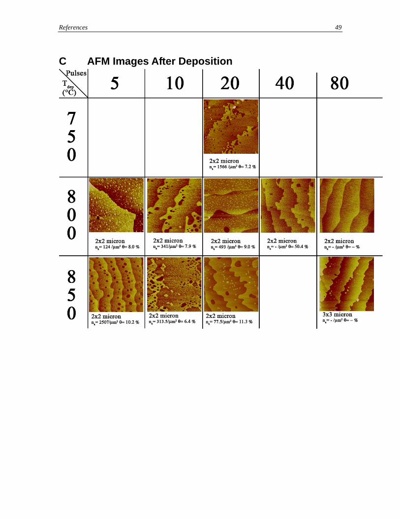
References 49
C AFM Images After Deposition

Nucleation and growth on SrTiO3 substrates characterized by ex-situ AFM 50

References 51
D Hystograms Cluster Height and Area Deposition at 750 °C, 20 pulses
Deposition at 800 °C, 5 pulses
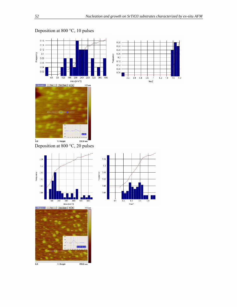
Nucleation and growth on SrTiO3 substrates characterized by ex-situ AFM 52
Deposition at 800 °C, 10 pulses
Deposition at 800 °C, 20 pulses
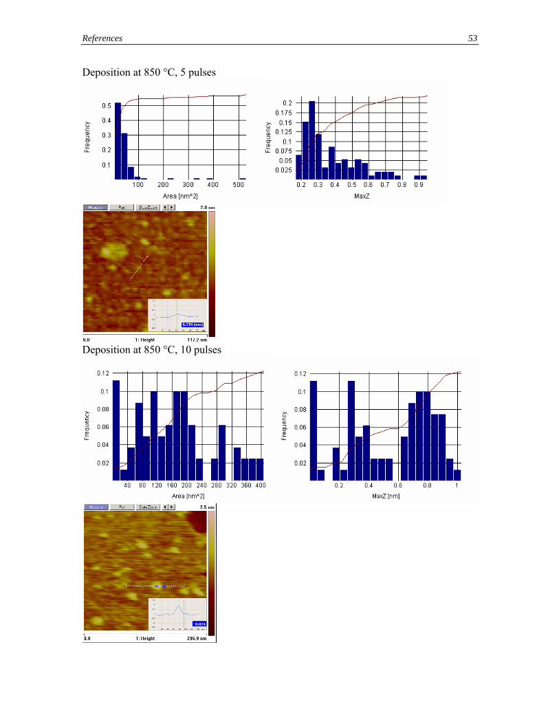
References 53
Deposition at 850 °C, 5 pulses
Deposition at 850 °C, 10 pulses

Nucleation and growth on SrTiO3 substrates characterized by ex-situ AFM 54
Deposition at 850 °C, 20 pulses
Symbols SrTiO3 Strontium Titanate, STO TiO2 Titanium dioxide AFM Atomic Force Microscopy BHF Buffer HF solution CM Contact Mode CVT Chemical Vapor Transport IMS Inorganic Materials Science LEED Low Energy Electron Diffraction PLD Pulsed Laser Deposition RHEED Reflection High-Energy Electron Diffraction SEM Scanning Electron Microscopy SPM Scanning Probe Microscopy STEM Scanning Tunneling Electron Microscopy STM Scanning Tunneling Microscopy STO Strontium Titanate, SrTiO3 SXRD Surface X-ray Diffraction TEM Tunneling Electron Microscopy TM Tapping Mode XRD X-ray Diffraction W Emitted energy by an object with Temperature T. R Deposition rate R Reflected energy on object t deposition time T Transmitted energy through object Ts Substrate temperature

Distribution List Prof. D.H.A. Blank, Dr. A.J.H.M. Rijnders, ir. J.J. Broekmaat Inorganic Materials Science Group Faculty of Science & Technology University of Twente P.O. Box 217 7500 AE Enschede The Netherlands
Dr. H. Schönherr University of Twente MTP LA 1360 PO Box 217 7500AE Enschede The Netherlands
ir, D.B. Bijl SmartTip B.V. PO Box 347 7500 AH, Enschede The Netherlands
A.H.G. Prinsen Kuipersdijk 101-A 7512 CC Enschede The Netherlands