Embed Size (px)
Citation preview

NSREC 2013 Summary
Radiation 2 Electronics (R2E) LHC Activities
NSREC 2013 Summary
Rubén García Alía, Giovanni Spiezia, Slawosz Uznanski

NSREC 2013 Summary2
Useful links
• Online brochure NSREC 2013: • http://www.nsrec.com/brochure2013.pdf
• Pre-print collection (not exhaustive and with non-uniform naming):• \\cern.ch\dfs\Departments\AB\Groups\ATB\LP\Equipment
Controls\Radmon and Radiation test facility\Conference_WS_scg\NSREC-13\pre-prints
• http://radwg.web.cern.ch/RadWG/Pages/Literature.htm• Online preprint request:
• http://www.nsrec.com/preprints2013.htm• Online data workshop record:
• http://nsrec.com/redw/

NSREC 2013 Summary3
Summary overview
• Dosimetry (optical fibers)• Destructive SEE events (Schottky diodes)• Test approach (high-speed SRAMs)• Component scaling (sensitivity to secondary protons +
electrons)• Laser testing (transistor analysis for deep sub-micron)• Moore’s law (FinFETs)
NSREC 2013 Summary4
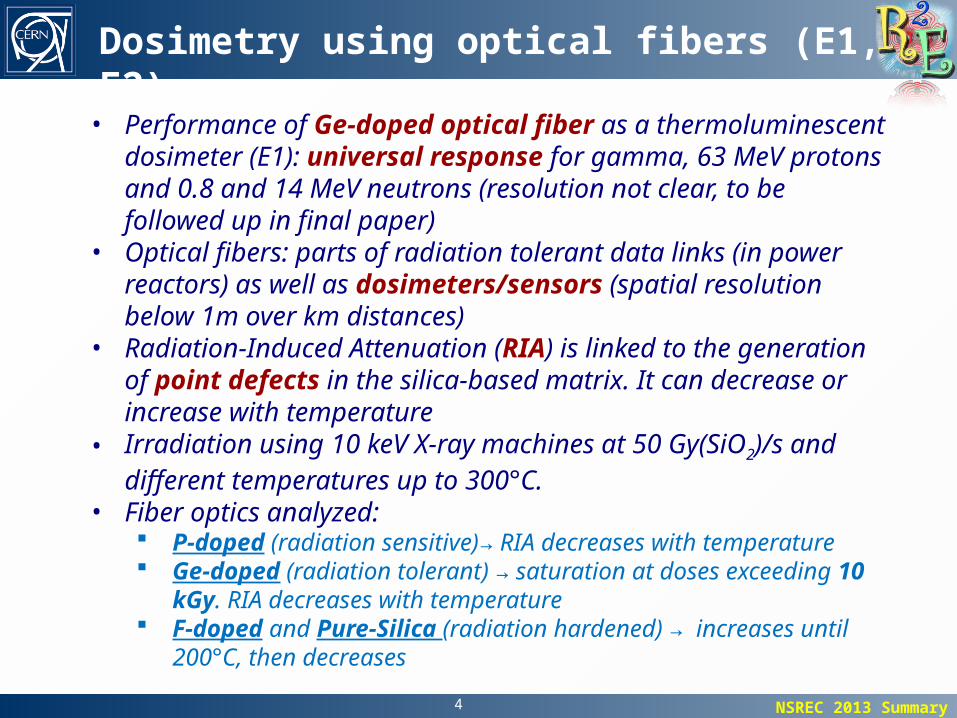
Dosimetry using optical fibers (E1, F2)
• Performance of Ge-doped optical fiber as a thermoluminescent dosimeter (E1): universal response for gamma, 63 MeV protons and 0.8 and 14 MeV neutrons (resolution not clear, to be followed up in final paper)
• Optical fibers: parts of radiation tolerant data links (in power reactors) as well as dosimeters/sensors (spatial resolution below 1m over km distances)
• Radiation-Induced Attenuation (RIA) is linked to the generation of point defects in the silica-based matrix. It can decrease or increase with temperature
• Irradiation using 10 keV X-ray machines at 50 Gy(SiO2)/s and different temperatures up to 300°C.
• Fiber optics analyzed: P-doped (radiation sensitive)→ RIA decreases with temperature Ge-doped (radiation tolerant) → saturation at doses exceeding 10 kGy.
RIA decreases with temperature F-doped and Pure-Silica (radiation hardened) → increases until 200°C,
then decreases

NSREC 2013 Summary5
Dosimetry using optical fibers (E1, F2)
Dosimetry with P-doped fibers: linear response for space and medical, and possible calibration for larger doses
Spectra domains where RIA is only very slightly affected by temperature can be exploited for dosimetry applications
S. Girard et al. “Combined High Dose and Temperature Radiation Effects on Multimode Silica-based Optical Fibers”, NSREC 2013 preprint

NSREC 2013 Summary6
Destructive events in Schottky diodes (W-35, I-1)
• Diodes used in hybrid DC-DC converters• Test performed on commercial parts SD090SC200A (Sensitron) and
MBRC20200CT (On Semiconductors) for heavy ions (both) and protons (the second)
• Failures occur in reverse voltage and cross sections are strongly dependent on voltage bias
• LET threshold at ~ 10-20 MeVcm2/mg for both devices, and proton cross section of 10-12 – 10-10 cm2/device depending on bias voltage (180-200V)
• Direct ionization from a charged particle is thought to be insufficient to cause a failure. Nuclear interactions are needed to trigger the event
• Tungsten used as contact metal. Cross section similar from back side than front side, therefore fragments from tungsten are ruled out as the cause (note: fission products are isotropic)

NSREC 2013 Summary7
Single Event Burnout
Destructive events in Schottky diodes (W-35, I-1)
Heavy Ion cross section
200 MeV proton cross section
J. George et al. “Single Event Burnout Observed in Schottky Diodes”, NSREC 2013 preprint

NSREC 2013 Summary8
At-Speed SEE SRAM testing (D-6)
• Advanced process technologies (sub-100 nm process) can operate at frequencies from several hundred MHz until greater than one GHz
• High performance SRAMs have low critical charge and often use EDAC codes that can reduce the number of events by 4 orders of magnitude
• Uncorrectable events (MBUs) can dominate the corrected error rate• Testing modes: W/RUF (Write/Read Until Failure) yields equivalent
results to Static, while W/R (Write/Read) provides a cross section ~1/2 that of Static (half the error are over-written)
• The nearly uninterrupted at-speed operation during the test can only be achieved with the data analyzed on-chip
• This test procedure allows for MCU and MBU detection, as well as transient (frequency dependent) and persistent error identification
• Dependence of the event multiplicity with the rotation angle (and large tilt angle) as more cells are

NSREC 2013 Summary9
At-Speed SEE SRAM testing (D-6)
SEU and MBU cross section for 32 nm tech. MBU dependence with rotation angle
0°
90°
E. Cannon et al. “At-Speed SEE Testing of RHBD Embedded SRAMs”, NSREC 2013 preprint
2x2 cell array for 90 nm SRAM

NSREC 2013 Summary10
Impact of secondary protons in terrestrial environments (PD-5)
• Tests performed on a 90 nm Fujitsu technology down to a supply voltage of 0.2V (nominal is 1.1V)
• Increase of a factor ~500 in the SER, however only a factor ~4 is expected from simulations shown in the work
• No pre-print of the paper available, but similar work can be found:
Kobayashi, H. et al. "Alpha particle and neutron-induced soft error rates and scaling trends in SRAM“, Reliability Physics Symposium, 2009 IEEE International , vol., no., pp.206,211, 26-30 April 2009
In an accelerator environment, the impact could be even stronger (direct ionization from environment particles, higher proton and alpha production due to larger energies…)

NSREC 2013 Summary11
Sub-micrometer laser spot size (D-3)
• Laser spot-size of 0.3 um (FWHM) for the analysis of single transistors in deep sub-micron technologies
• 90 nm SRAM studied, with a cell surface of 0.7 x 1.6 um2 and a transistor size in the order of 0.2 um
• Analysis of individual transistor sensitivity yields a very large intra-cell spread with a regular pattern, and is therefore attributed to the masking used to produce the chip
45 nm memory cell covered by a 1 um spot-size
Schwank, J. et al. “Estimation of Heavy-Ion LET Threshold in Advanced SOI IC Technologies From Two-Photon Absorption Laser Measurements“ Nuclear Science, IEEE Transactions on , vol.57, no.4, pp.1827,1834, Aug. 2010

NSREC 2013 Summary12
Electron induced SEUs (C-1)
• First experimental evidence of SEU induction by a single electron• 45 nm technology used: Qcrit is estimated to be 0.38 fC for 1.1V
(nominal) operation and 0.19 fC for 0.55V (corresponding to 8.6 and 4.3 keV respectively)
• Upsets only measured in the Vsupply=Vnominal/2, consistent with simulations
• Physical process: X-ray beam (10 keV photons) which can undergo photoabsorption,
transmitting almost all their kinetic energy to electrons Auger decay chain (internal absorption) can also deposit enough
energy to cause an SEU• Cell size simulated as 0.16 um2 x 300 nm• Note: the SEU cannot in principle be induced through direct ionization
as the range in silicon of a 10 keV electron is 1.5 um (too large in relation to the deep sub-micron transistor size)

NSREC 2013 Summary13
Technology scaling: FinFETs (H2, J2, J3)
• FinFETs are the trend solution for component scaling below 28 nm thanks to their low leakage characteristics (Samsung, IBM, Global Foundries, Intel…)
• High-K gate oxide materials (HfO2) needed as leakage currents increase dramatically for SiO2 with thicknesses below 2 nm
• Gate breakdown in SRAM memory transistors• operation voltages could go down to 0.4-0.6V (for power efficiency,
exascale computing being the driving application)
• Two main FinFET types:• bulk (SEU prone, minor TID
effects but still there due to the oxides in the STI)
• SOI (no charge sharing, less prone to SEU, TID effects in buried oxide)


![mapa [re]activo issuu€¦ · compite o se alía con la presencia construida para conjuntamente definir la arquitectura de la ciudad. No es un añadido o una condición, es una parte](https://img.pdfslide.us/doc/110x75/5eb9959967437f79cb381bd0/mapa-reactivo-issuu-compite-o-se-ala-con-la-presencia-construida-para-conjuntamente.jpg)