Embed Size (px)
Citation preview
NS9775 Hardware Reference
90000524_E

Part number/version: 90000524_ERelease date: March 2008www.digi.com
NS9775 Hardware Reference

Digi International11001 Bren Road EastMinnetonka, MN 55343 U.S.A.United States: +1 877 912-3444Other locations: +1 952 912-3444
www.digi.com/support/www.digi.com
©2008 Digi International Inc.Printed in the United States of America. All rights reserved.
Digi, Digi International, the Digi logo, the Making Device Networking Easy logo, NetSilicon, a Digi International Company, NET+, NET+OS and NET+Works are trademarks or registered trademarks of Digi International, Inc. in the United States and other countries worldwide. All other trademarks are the property of their respective owners.
Information in this document is subject to change without notice and does not represent a committment on the part of Digi International.
Digi provides this document “as is,” without warranty of any kind, either expressed or implied, including, but not limited to, the implied warranties of, fitness or merchantability for a particular purpose. Digi may make improvements and/or changes in this manual or in the product(s) and/or the program(s) described in this manual at any time.
This product could include technical inaccuracies or typographical errors. Changes are made periodically to the information herein; these changes may be incorporated in new editions of the publication.
Contents
i i i
Documentation updates ............................................................. xxiv
C h a p t e r 1 : A b o u t N S 9 7 7 5 .................................................................. 1
NS9775 Features ......................................................................... 2System-level interfaces................................................................. 9System boot ............................................................................. 11Reset...................................................................................... 11
RESET_DONE as an input........................................................ 12RESET_DONE as an output ...................................................... 12
System clock............................................................................. 14Printer video clock ..................................................................... 16USB clock................................................................................. 18
C h a p t e r 2 : N S 9 7 7 5 P i n o u t ................................................................ 21
Pinout and signal descriptions ........................................................ 22System Memory interface ...................................................... 22System Memory interface signals.............................................. 26Ethernet interface............................................................... 29Clock generation/system pins ................................................. 30bist_en_n, pll_test_n, and scan_en_n........................................ 31PCI interface...................................................................... 32GPIO MUX ......................................................................... 38LCD module signals .............................................................. 45Printer engine interface ........................................................ 45I2C interface...................................................................... 47
iv
USB interface..................................................................... 47JTAG interface for ARM core/boundary scan................................ 47Reserved .......................................................................... 49Power ground..................................................................... 49
C h a p t e r 3 : W o r k i n g w i t h t h e C P U ............................................... 51
About the processor.................................................................... 52Instruction sets.......................................................................... 53
ARM instruction set.............................................................. 54Thumb instruction set........................................................... 54Java instruction set ............................................................. 54
System control processor (CP15) registers.......................................... 55ARM926EJ-S system addresses ................................................. 55Accessing CP15 registers........................................................ 56Terms and abbreviations ....................................................... 56Register summary................................................................ 57R0: ID code and cache type status registers................................. 59R1: Control register ............................................................. 62R2: Translation Table Base register........................................... 65R3: Domain Access Control register........................................... 65R4 register ........................................................................ 66R5: Fault Status registers....................................................... 66R6: Fault Address register ...................................................... 68R7: Cache Operations register ................................................. 68R8:TLB Operations register..................................................... 72R9: Cache Lockdown register .................................................. 74R10: TLB Lockdown register.................................................... 77R11 and R12 registers ........................................................... 78R13: Process ID register......................................................... 79R14 register....................................................................... 81R15: Test and debug register .................................................. 81
Jazelle (Java) ........................................................................... 81DSP........................................................................................ 82Memory Management Unit (MMU) .................................................... 82
MMU Features .................................................................... 82Address translation .............................................................. 85MMU faults and CPU aborts..................................................... 99
v
Domain access control .........................................................102Fault checking sequence ......................................................103External aborts..................................................................106Enabling the MMU...............................................................107Disabling the MMU ..............................................................108TLB structure ....................................................................108
Caches and write buffer ..............................................................109Cache features ..................................................................109Write buffer .....................................................................110Enabling the caches ............................................................111Cache MVA and Set/Way formats ............................................113
Noncachable instruction fetches ....................................................115Self-modifying code ............................................................116AHB behavior ....................................................................116
Instruction Memory Barrier...........................................................117IMB operation....................................................................117Sample IMB sequences .........................................................118
C h a p t e r 4 : S y s t e m C o n t r o l M o d u l e ........................................... 119
System Control Module features ....................................................120Bus interconnection ...................................................................120System bus arbiter.....................................................................120
Arbiter configuration examples ..............................................124AHB bus error monitoring......................................................127
Address decoding ......................................................................128Programmable timers .................................................................130
Software watchdog timer......................................................130General purpose timers/counters ............................................130
Interrupt controller ...................................................................134Vectored interrupt controller (VIC) flow....................................137
System attributes......................................................................137PLL configuration ...............................................................138Bootstrap initialization ........................................................139
System configuration registers ......................................................143AHB Arbiter Gen Configuration register .....................................149BRC0, BRC1, BRC2, and BRC3 registers......................................150
vi
AHB Bus Arbiter Timeout Period/AHB Bus Monitor Timeout Period register151AHB Error Status 1 ..............................................................152AHB Error Status 2 ..............................................................153AHB Error Monitoring Configuration register ...............................155Timer 0–15 Reload Count registers...........................................156Timer 0–15 Read register ......................................................157Interrupt Vector Address Register Level 0–31 ..............................157Int (Interrupt) Config (Configuration) registers (0–31) ....................158ISRADDR register ................................................................160Interrupt Status Active.........................................................161Interrupt Status Raw ...........................................................162Timer Interrupt Status register ...............................................163Software Watchdog Configuration register .................................163Software Watchdog Timer register ..........................................165Clock Configuration register ..................................................165Reset and Sleep Control register .............................................167Miscellaneous System Configuration and Status register .................169PLL Configuration register.....................................................171Active Interrupt Level Status register .......................................173Timer 0–15 Control registers ..................................................174System Memory Chip Select 0 Dynamic Memory Base and Mask registers..176System Memory Chip Select 1 Dynamic Memory Base and Mask registers..177System Memory Chip Select 2 Dynamic Memory Base and Mask registers..178System Memory Chip Select 3 Dynamic Memory Base and Mask registers..179System Memory Chip Select 0 Static Memory Base and Mask registers.180System Memory Chip Select 1 Static Memory Base and Mask registers.181System Memory Chip Select 2 Static Memory Base and Mask registers.182System Memory Chip Select 3 Static Memory Base and Mask registers.183Gen ID register ..................................................................184External Interrupt 0–3 Control register......................................185
C h a p t e r 5 : M e m o r y C o n t r o l l e r ..................................................... 187
Features.................................................................................188
v i i
System overview ................................................................189Low-power operation ..........................................................190Memory map.....................................................................190
Static memory controller.............................................................192Write protection ................................................................193Extended wait transfers .......................................................194Memory mapped peripherals..................................................194Static memory initialization ..................................................194Byte lane control ...............................................................221Address connectivity ...........................................................222Byte lane control and databus steering .....................................227
Dynamic memory controller .........................................................235Write protection ................................................................235Access sequencing and memory width ......................................235Address mapping................................................................236
Registers ................................................................................275Register map ....................................................................275Reset values .....................................................................277Control register .................................................................278Status register...................................................................280Configuration register..........................................................281Dynamic Memory Control register............................................282Dynamic Memory Refresh Timer register ...................................283Dynamic Memory Read Configuration register .............................285Dynamic Memory Precharge Command Period register ...................286Dynamic Memory Active to Precharge Command Period register .......287Dynamic Memory Self-refresh Exit Time register ..........................288Dynamic Memory Last Data Out to Active Time register .................289Dynamic Memory Data-in to Active Command Time register ............290Dynamic Memory Write Recovery Time register ...........................291Dynamic Memory Active to Active Command Period register............292Dynamic Memory Auto Refresh Period register ............................293Dynamic Memory Exit Self-refresh register .................................294Dynamic Memory Active Bank A to Active Bank B Time register ........295Dynamic Memory Load Mode register to Active Command Time register..296Static Memory Extended Wait register ......................................297Dynamic Memory Configuration 0–3 registers ..............................298
viii
Dynamic Memory RAS and CAS Delay 0–3 registers ........................302Static Memory Configuration 0–3 registers..................................303Static Memory Write Enable Delay 0–3 registers ...........................307Static Memory Output Enable Delay 0–3 registers .........................308Static Memory Read Delay 0–3 registers.....................................309Static Memory Page Mode Read Delay 0–3 registers.......................310Static Memory Write Delay 0–3 registers ....................................311Static Memory Turn Round Delay 0–3 registers.............................312
C h a p t e r 6 : E t h e r n e t C o m m u n i c a t i o n M o d u l e ....................... 325
Overview ................................................................................326Ethernet MAC...........................................................................327
Station address logic (SAL) ....................................................331Statistics module ...............................................................331
Ethernet front-end module ..........................................................333Receive packet processor .....................................................334Transmit packet processor ....................................................337Ethernet Slave Interface.......................................................341Interrupts ........................................................................341Resets.............................................................................342
External CAM filtering ................................................................343Ethernet Control and Status registers ..............................................346
Ethernet General Control Register #1 .......................................348Ethernet General Control Register #2 .......................................352Ethernet General Status register.............................................354Ethernet Transmit Status register............................................354Ethernet Receive Status register .............................................358MAC Configuration Register #1 ...............................................360MAC Configuration Register #2 ...............................................361Back-to-Back Inter-Packet-Gap register.....................................364Non Back-to-Back Inter-Packet-Gap register ...............................365Collision Window/Retry register .............................................366Maximum Frame register ......................................................367PHY Support register ...........................................................368MII Management Configuration register .....................................369MII Management Command register..........................................371MII Management Address register ............................................372
i x
MII Management Write Data register ........................................372MII Management Read Data register .........................................373MII Management Indicators register..........................................374Station Address registers ......................................................375Station Address Filter register ................................................377Register Hash Tables ...........................................................377Statistics registers ..............................................................379RX_A Buffer Descriptor Pointer register.....................................394RX_B Buffer Descriptor Pointer register.....................................394RX_C Buffer Descriptor Pointer register.....................................395RX_D Buffer Descriptor Pointer register ....................................395Ethernet Interrupt Status register ...........................................396Ethernet Interrupt Enable register...........................................398TX Buffer Descriptor Pointer register........................................400Transmit Recover Buffer Descriptor Pointer register .....................400TX Error Buffer Descriptor Pointer register.................................401TX Stall Buffer Descriptor Pointer register .................................402RX_A Buffer Descriptor Pointer Offset register ............................403RX_B Buffer Descriptor Pointer Offset register ............................404RX_C Buffer Descriptor Pointer Offset register ............................405RX_D Buffer Descriptor Pointer Offset register ............................405Transmit Buffer Descriptor Pointer Offset register........................406RX Free Buffer register ........................................................407TX buffer descriptor RAM......................................................408
Sample hash table code ..............................................................409
C h a p t e r 7 : P C I - t o - A H B B r i d g e ...................................................... 415
About the PCI-to-AHB Bridge ........................................................416PCI-to-AHB bridge functionality ..............................................417Cross-bridge transaction error handling.....................................419AHB address decoding and translation ......................................420PCI address decoding and mapping ..........................................421Interrupts ........................................................................421Transaction ordering ...........................................................423Endian configuration ...........................................................423Configuration registers.........................................................423Bridge Configuration registers ................................................425
x
PCI bus arbiter .........................................................................431PCI arbiter functional description............................................431Slave interface ..................................................................433PCI Arbiter Configuration registers ..........................................433
PCI system configurations ............................................................469Device selection for configuration ...........................................471PCI interrupts....................................................................472PCI central resource functions................................................472
CardBus Support .......................................................................474Configuring NS9775 for CardBus support ....................................476CardBus adapter requirements ...............................................478CardBus interrupts..............................................................478
C h a p t e r 8 : B B u s B r i d g e .................................................................... 479
BBus bridge functions .................................................................480Bridge control logic ...................................................................481
DMA accesses ....................................................................483BBus control logic .....................................................................484
BBus bridge masters and slaves...............................................484Cycles and BBus arbitration ...................................................485BBus peripheral address map (decoding) ...................................485
Two-channel AHB DMA controller (AHB bus) ......................................486DMA buffer descriptor..........................................................486Descriptor list processing......................................................488Peripheral DMA read access...................................................489Peripheral DMA write access ..................................................490Peripheral REQ signaling.......................................................491Design Limitations ..............................................................492Calculating AHB DMA response latency......................................492Static RAM chip select configuration ........................................494
Interrupt aggregation .................................................................495Bandwidth requirements .............................................................495SPI-EEPROM boot logic ................................................................496
Serial Channel B configuration ...............................................496Memory Controller configuration.............................................497SDRAM boot algorithm .........................................................500
x i
BBus Bridge Control and Status registers ..........................................501Buffer Descriptor Pointer register............................................502DMA Channel 1/2 Control register ...........................................503DMA Status and Interrupt Enable register...................................506DMA Peripheral Chip Select register .........................................508BBus Bridge Interrupt Status register........................................509BBus Bridge Interrupt Enable register .......................................510
C h a p t e r 9 : B B u s D M A C o n t r o l l e r ................................................ 513
About the BBus DMA controllers.....................................................514DMA context memory .................................................................515DMA buffer descriptor ................................................................516DMA channel assignments ............................................................521DMA Control and Status registers ...................................................523
DMA Buffer Descriptor Pointer................................................525DMA Control register ...........................................................526DMA Status/Interrupt Enable register .......................................528
C h a p t e r 1 0 : B B u s U t i l i t y ................................................................. 533
BBus Utility Control and Status registers ..........................................534Master Reset register...........................................................535GPIO Configuration registers..................................................535GPIO Control registers .........................................................541GPIO Status registers...........................................................544BBus Monitor register ..........................................................547BBus DMA Interrupt Status register ..........................................548BBus DMA Interrupt Enable register..........................................549USB Configuration register ....................................................550Endian Configuration register.................................................551ARM Wake-up register..........................................................553
C h a p t e r 1 1 : I 2 C M a s t e r / S l a v e I n t e r f a c e ................................ 555
Overview ................................................................................556Physical I2C bus .................................................................556
I2C external addresses................................................................557I2C command interface ...............................................................557
xii
Locked interrupt driven mode ................................................558Master module and slave module commands...............................558Bus arbitration ..................................................................559
I2C registers ............................................................................559Command Transmit Data register ............................................560Status Receive Data register ..................................................561Master Address register ........................................................562Slave Address register..........................................................563Configuration register..........................................................564
Interrupt Codes ........................................................................565Software driver ........................................................................567Flow charts .............................................................................568
Master module (normal mode, 16-bit).......................................568Slave module (normal mode, 16-bit) ........................................569
C h a p t e r 1 2 : L C D C o n t r o l l e r ........................................................... 571
LCD features............................................................................572Programmable parameters ....................................................572LCD panel resolution ...........................................................573LCD panel support ..............................................................573Number of colors ...............................................................574LCD power up and power down sequence support ........................575
LCD controller functional overview.................................................576Clocks.............................................................................577Signals and interrupts ..........................................................578
AHB interface ..........................................................................580AHB master and slave interfaces .............................................580Dual DMA FIFOs and associated control logic...............................580Pixel serializer ..................................................................581RAM palette......................................................................585Grayscaler .......................................................................586Upper and lower panel formatters...........................................586Panel clock generator..........................................................586Timing controller ...............................................................586Generating interrupts ..........................................................587External pad interface signals ................................................587LCD panel signal multiplexing details .......................................587
x i i i
Registers ................................................................................591LCDTiming0 ......................................................................591LCDTiming1 ......................................................................594LCDTiming2 register............................................................596LCDTiming3 ......................................................................599LCDUPBASE and LCDLPBASE ...................................................599LCDINTRENABLE .................................................................601LCDControl register.............................................................602LCDStatus register ..............................................................605LCDInterrupt register ..........................................................606LCDUPCURR and LCDLPCURR..................................................607LCDPalette register.............................................................608
Interrupts ...............................................................................611MBERRORINTR — Master bus error interrupt................................611VCOMPINTR — Vertical compare interrupt..................................611LBUINTR — Next base address update interrupt ...........................612
C h a p t e r 1 3 : S e r i a l C o n t r o l M o d u l e : U A R T ............................ 613
Features.................................................................................614Bit-rate generator ..............................................................615
UART mode .............................................................................616 FIFO management ....................................................................617
Transmit FIFO interface .......................................................617Receive FIFO interface.........................................................618
Serial port performance ..............................................................620Serial port control and status registers ............................................620
Serial Channel B/A/C/D Control Register A ................................623Serial Channel B/A/C/D Control Register B ................................627Serial Channel B/A/C/D Status Register A ..................................630Serial Channel B/A/C/D Bit-rate register ...................................637Serial Channel B/A/C/D FIFO Data register ................................644Serial Channel B/A/C/D Receive Buffer GAP Timer .......................645Serial Channel B/A/C/D Receive Character GAP Timer ..................646Serial Channel B/A/C/D Receive Match register...........................648Serial Channel B/A/C/D Receive Match MASK register ...................649Serial Channel B/A/C/D Flow Control register.............................650Serial Channel B/A/C/D Flow Control Force register .....................652
xiv
C h a p t e r 1 4 : S e r i a l C o n t r o l M o d u l e : S P I ................................ 655
Features.................................................................................656Bit-rate generator ..............................................................657
SPI mode ................................................................................658SPI modes ........................................................................658
FIFO management .....................................................................659Transmit FIFO interface .......................................................659Receive FIFO interface.........................................................660
Serial port performance ..............................................................662Serial port control and status registers ............................................662
Serial Channel B/A/C/D Control Register A ................................664Serial Channel B/A/C/D Control Register B ................................667Serial Channel B/A/C/D Status Register A ..................................669Serial Channel B/A/C/D Bit-rate register ...................................674Serial Channel B/A/C/D FIFO Data register ................................679Serial Channel B/A/C/D Receive Buffer GAP Timer.......................680Serial Channel B/A/C/D Receive Character GAP Timer ..................681Serial Channel B/A/C/D Receive Match register...........................683Serial Channel B/A/C/D Receive Match MASK register ...................684
C h a p t e r 1 5 : I E E E 1 2 8 4 P e r i p h e r a l C o n t r o l l e r ..................... 685
Requirements ..........................................................................686Overview ................................................................................686
Compatibility mode ............................................................687Nibble mode .....................................................................688Byte mode .......................................................................688ECP mode ........................................................................689Data and command FIFOs......................................................691IEEE 1284 negotiation ..........................................................692
BBus slave and DMA interface .......................................................693BBus slave and DMA interface register map ................................693IEEE 1284 General Configuration register...................................695Interrupt Status and Control register........................................697FIFO Status register ............................................................700Forward Command FIFO Read register ......................................702Forward Data FIFO Read register.............................................703
xv
Reverse FIFO Write register/Reverse FIFO Write Register — Last.......703Forward Command DMA Control register ...................................705Forward Data DMA Control register ..........................................706Printer Data Pins register......................................................707Port Status register, host......................................................708Port Control register ...........................................................709Port Status register, peripheral ..............................................710Feature Control Register A ....................................................710Feature Control Register B ....................................................711Interrupt Enable register ......................................................711Master Enable register .........................................................713Extensibility Byte Requested by Host........................................714Extended Control register .....................................................714Interrupt Status register .......................................................715Pin Interrupt Mask register ....................................................716Pin Interrupt Control register.................................................717Granularity Count register ....................................................718Forward Address register ......................................................719Core Phase (IEEE1284) register ...............................................720
C h a p t e r 1 6 : U S B C o n t r o l l e r M o d u l e .......................................... 723
Overview ................................................................................724USB module architecture .............................................................724USB device block.......................................................................726
Control and status ..............................................................726Packet and data flow...........................................................727Logical and physical endpoints ...............................................728Slew rates........................................................................728
Host block...............................................................................728Control and status ..............................................................728Packet data flow................................................................729
USB device endpoint ..................................................................730Transmission error handling..........................................................730
Handling USB-IN packet errors................................................731Handling USB-OUT packet errors .............................................731
USB block registers ....................................................................732USB Global registers...................................................................732
xvi
Global Control and Status register ...........................................733Device Control and Status register...........................................734Global Interrupt Enable register .............................................736Global Interrupt Status register ..............................................738Device IP Programming Control/Status register ...........................740
USB host block registers ..............................................................741Reserved bits ....................................................................741USB host block register address map ........................................742HCRevision register.............................................................743HcControl register ..............................................................743HcCommandStatus register ...................................................747HcInterruptStatus register.....................................................750HcInterruptEnable register ....................................................752HcInterruptDisable register ...................................................754HcHCCA register ................................................................756HcPeriodCurrentED register...................................................757HcControlHeadED register.....................................................758HcControlCurrentED register..................................................759HcBulkHeadED register ........................................................760HcBulkCurrentED register .....................................................761HcDoneHead register...........................................................763HcFmInterval register ..........................................................764HcFmRemaining register.......................................................765HcFmNumber register..........................................................766HcPeriodicStart register .......................................................767HcLsThreshold register.........................................................768Root hub partition registers...................................................769HcRhDescriptorA register......................................................770HcRhStatus register ............................................................773HcRhPortStatus[1] register ....................................................776
USB Device Block registers ...........................................................782Device Descriptor/Setup Command register................................782Endpoint Descriptor #0–#11 registers ........................................783
USB Device Endpoint FIFO Control and Data registers ...........................784FIFO Interrupt Status registers ...............................................786FIFO Interrupt Enable registers...............................................793FIFO Packet Control registers.................................................798
xv i i
FIFO Status and Control registers ............................................799
C h a p t e r 1 7 : T i m i n g ............................................................................. 803
Electrical characteristics .............................................................804Absolute maximum ratings ....................................................804Recommended operating conditions.........................................804Maximum power dissipation...................................................805Typical power dissipation .....................................................805
DC electrical characteristics.........................................................806Inputs .............................................................................806Outputs...........................................................................807
Power sequencing .....................................................................808Memory timing .........................................................................809
SDRAM burst read (16-bit) .....................................................810SDRAM burst read (16-bit), CAS latency = 3 ................................811SDRAM burst write (16-bit) ....................................................812SDRAM burst read (32-bit) .....................................................813SDRAM burst read (32-bit), CAS latency = 3 ................................814SDRAM burst write (32-bit) ....................................................815SDRAM load mode...............................................................816SDRAM refresh mode ...........................................................817Clock enable timing ............................................................817Static RAM read cycles with 0 wait states ..................................819Static RAM asynchronous page mode read, WTPG = 1 ....................820Static RAM read cycle with configurable wait states .....................821Static RAM sequential write cycles ..........................................822Static RAM write cycle .........................................................823Static write cycle with configurable wait states...........................824
Ethernet timing ........................................................................825Ethernet MII timing .............................................................826Ethernet RMII timing ...........................................................827
PCI timing...............................................................................828Internal PCI arbiter timing ....................................................830PCI burst write from NS9775 timing .........................................830PCI burst read from NS9775 timing ..........................................831PCI burst write to NS9775 timing.............................................831PCI burst read to NS9775 timing..............................................832
xviii
PCI clock timing.................................................................832I2C timing ...............................................................................833LCD timing ..............................................................................834
Horizontal timing for STN displays ...........................................836Vertical timing for STN displays ..............................................837Horizontal timing for TFT displays ...........................................837Vertical timing for TFT displays ..............................................837HSYNC vs VSYNC timing for STN displays....................................838HSYNC vs VSYNC timing for TFT displays....................................838LCD output timing ..............................................................838
SPI timing ...............................................................................839SPI master mode 0 and 1: 2-byte transfer ..................................841SPI master mode 2 and 3: 2-byte transfer ..................................841SPI slave mode 0 and 1: 2-byte transfer ....................................842SPI slave mode 2 and 3: 2-byte transfer ....................................842
IEEE 1284 timing .......................................................................843IEEE 1284 timing example .....................................................843
USB timing ..............................................................................844USB differential data timing ..................................................845USB full speed load timing ....................................................845USB low speed load.............................................................846
Reset and hardware strapping timing ..............................................847JTAG timing ............................................................................848Clock timing ............................................................................849
USB crystal/external oscillator timing ......................................849LCD input clock timing.........................................................850System PLL bypass mode timing..............................................851
C h a p t e r 1 8 : P a c k a g i n g ..................................................................... 853
Product specifications .........................................................857

x i x

Using This Guide
xx i
Review this section for basic information about the guide you are using, as well as general support and contact information.
About this guide
This guide provides information about the Digi NS9775, a single chip 0.13μm CMOS network-attached processor. The NS9775 is part of the Digi NET+ARM family of devices.
The NET+ARM family is part of the NET+Works integrated product family, which includes the NET+OS network software suite.
Who should read this guide
This guide is for hardware developers, system software developers, and applications programmers who want to use the NS9775 for development.
To complete the tasks described in this guide, you must:
Understand the basics of hardware and software design, operating systems, and microprocessor design.
Understand the NS9775 architecture.
Using This Guide
x x i i NS9775 Ha r dwa r e Re f e r ence
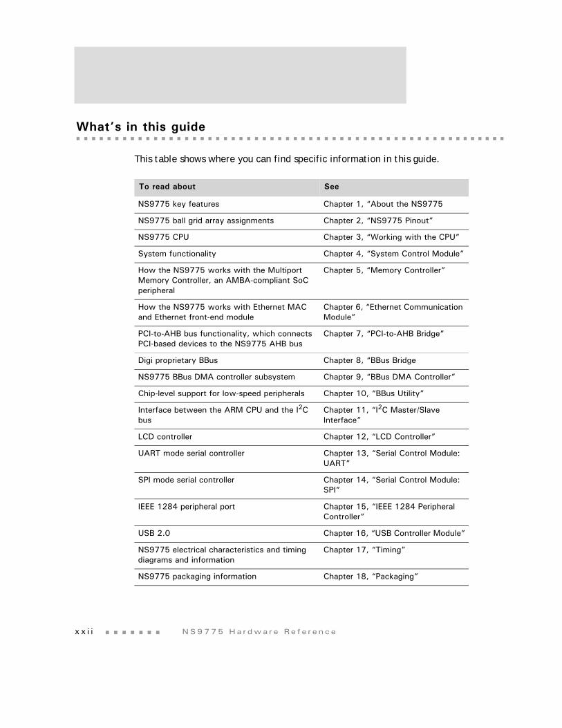
What’s in this guide
This table shows where you can find specific information in this guide.
To read about See
NS9775 key features Chapter 1, “About the NS9775
NS9775 ball grid array assignments Chapter 2, “NS9775 Pinout”
NS9775 CPU Chapter 3, “Working with the CPU”
System functionality Chapter 4, “System Control Module”
How the NS9775 works with the Multiport Memory Controller, an AMBA-compliant SoC peripheral
Chapter 5, “Memory Controller”
How the NS9775 works with Ethernet MAC and Ethernet front-end module
Chapter 6, “Ethernet Communication Module”
PCI-to-AHB bus functionality, which connects PCI-based devices to the NS9775 AHB bus
Chapter 7, “PCI-to-AHB Bridge”
Digi proprietary BBus Chapter 8, “BBus Bridge
NS9775 BBus DMA controller subsystem Chapter 9, “BBus DMA Controller”
Chip-level support for low-speed peripherals Chapter 10, “BBus Utility”
Interface between the ARM CPU and the I2C bus
Chapter 11, “I2C Master/Slave Interface”
LCD controller Chapter 12, “LCD Controller”
UART mode serial controller Chapter 13, “Serial Control Module: UART”
SPI mode serial controller Chapter 14, “Serial Control Module: SPI”
IEEE 1284 peripheral port Chapter 15, “IEEE 1284 Peripheral Controller”
USB 2.0 Chapter 16, “USB Controller Module”
NS9775 electrical characteristics and timing diagrams and information
Chapter 17, “Timing”
NS9775 packaging information Chapter 18, “Packaging”
www.d i g i . com xx i i i
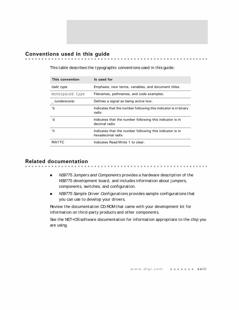
Conventions used in this guide
This table describes the typographic conventions used in this guide:
Related documentation
NS9775 Jumpers and Components provides a hardware description of the NS9775 development board, and includes information about jumpers, components, switches, and configuration.
NS9775 Sample Driver Configurations provides sample configurations that you can use to develop your drivers.
Review the documentation CD-ROM that came with your development kit for information on third-party products and other components.
See the NET+OS software documentation for information appropriate to the chip you are using.
This convention Is used for
italic type Emphasis, new terms, variables, and document titles.
monospaced type Filenames, pathnames, and code examples.
_ (underscore) Defines a signal as being active low.
‘b Indicates that the number following this indicator is in binary radix
‘d Indicates that the number following this indicator is in decimal radix
‘h Indicates that the number following this indicator is in hexadecimal radix
RW1TC Indicates Read/Write 1 to clear.
Documen t a t i on upda t e s
x x i v NS9775 Ha r dwa r e Re f e r ence
Documentation updates
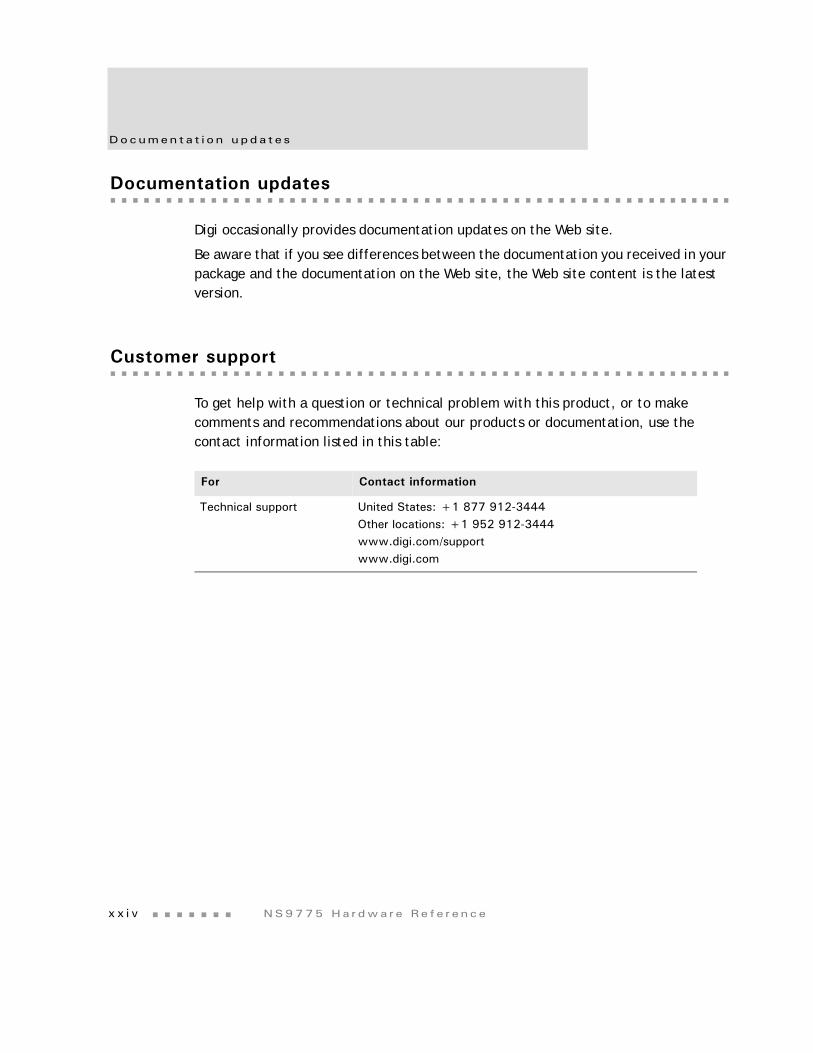
Digi occasionally provides documentation updates on the Web site.
Be aware that if you see differences between the documentation you received in your package and the documentation on the Web site, the Web site content is the latest version.
Customer support
To get help with a question or technical problem with this product, or to make comments and recommendations about our products or documentation, use the contact information listed in this table:
For Contact information
Technical support United States: +1 877 912-3444Other locations: +1 952 912-3444www.digi.com/supportwww.digi.com
1
About NS9775C H A P T E R 1
The Digi NS9775 is a high-performance, 32-bit microprocessor for color network printers and multi-function devices. This chapter provides an overview of the NS9775, which is based on the standard architecture in the NET+ARM family of devices.
NS9775 Fea t u r e s
2 NS9775 Ha r dwa r e Re f e r ence
NS9775 Features
The NS9775 integrates an ARM926EJ-S processor core with 10/100BaseT Ethernet, USB, IEEE 1284 interfaces, a 4-channel video interface with four inline JBIG decompressors, LCD controller, serial ports, memory controller, and a PCI/CardBus interface. The NS9775 ARM926EJ-S 32-bit RISC processor core runs at 200 MHz, with 8 kB of instruction cache and 4 kB of data cache.
One of the NS9775’s unique features is its four-channel video interface, which supports monochrome, 4-color, and tandem color laser print engines. The video interface is connected directly to four JBIG decompressors that allow simultaneous decompression of four color planes in parallel.
32-bit ARM926EJ-S RISC processor200 MHz
5-stage pipeline with interlocking
Harvard architecture
8 kB instruction cache and 4 kB data cache
32-bit ARM and 16-bit Thumb instruction sets. Can be mixed for performance/code density tradeoffs.
MMU to support virtual memory-based OSs, such as Linux, WinCE/Pocket PC, VxWorks, others
DSP instruction extensions, improved divide, single cycle MAC
ARM Jazelle, 1200CM (coffee marks) Java accelerator
EmbeddedICE-RT debug unit
JTAG boundary scan, BSDL support
Print engine controllerFour parallel JBIG decoders
– Internal bypass for uncompressed data
– Automatic and manual header processing modes
Glueless interface to most print engines
– 4 data ports for color tandem printers
– Single port for 4-pass color printers
– Single port for monochrome printers
www.d i g i . com 3
Abou t NS9775
Up to 13” lines at 2400 dpi
High print speed:
– Tandem: 90 ppm
– 4-pass color: 22 ppm
– Monochrome: 90 ppm
These conditions yield the above performance:
– Page size: 8.5” x 11”
– Resolution: 600 x 600 dpi
– Video clock: 100 MHz
– Horizontal correction factor: 0.7
– Vertical correction factor: 0.7
Synchronous print mode with internal PLL
– Clock rates up to 100 MHz
Asynchronous print mode with 1or 4 external clocks
– Clock rates up to 200 MHz
Bus Master on the system bus and a dedicated 4-channel DMA engine, one per colorplane
On-chip input and output FIFOs, one pair per color plane
General communication through serial and GPIO ports
External system bus interface32-bit data, 32-bit internal address bus, 28-bit external address bus
Glueless interface to SDRAM, SRAM, EEPROM, buffered DIMM, Flash
4 static and 4 dynamic memory chip selects
0–63 wait states per chip select
Self-refresh during system sleep mode
Automatic dynamic bus sizing to 8 bits, 16 bits, 32 bits
Burst mode support with automatic data width adjustment
Two external DMA channels for external peripheral support
NS9775 Fea t u r e s
4 NS9775 Ha r dwa r e Re f e r ence
System BootHigh-speed boot from 8-bit, 16-bit, or 32-bit ROM or Flash
Hardware-supported low cost boot from serial EEPROM through SPI port (patent pending)
High performance 10/100 Ethernet MAC10/100 Mbps MII/RMII PHY interfaces
Full-duplex or half-duplex
Station, broadcast, or multicast address filtering
2 kB RX FIFO
256-byte TX FIFO with on-chip buffer descriptor ring
– Eliminates underruns and decreases bus traffic
Separate TX and RX DMA channels
Intelligent receive-side buffer size selection
Full statistics gathering support
External CAM filtering support
PCI/CardBus portPCI v2.2, 32-bit bus, up to 33 MHz bus speed
Programmable to:
– PCI device mode
– PCI host mode:
Supports up to 3 external PCI devices
Embedded PCI arbiter or external arbiter
CardBus host mode
www.d i g i . com 5
Abou t NS9775
Flexible LCD controllerSupports most commercially available displays:
– Active Matrix color TFT displays:
Up to 24bpp direct 8:8:8 RGB; 16 colors
– Single and dual panel color STN displays:
Up to 16bpp 4:4:4 RGB; 3375 colors
– Single and dual panel monochrome STN displays:
1, 2, 4bpp palettized gray scale
Formats image data and generates timing control signals
Internal programmable palette LUT and grayscaler support different color techniques
Programmable panel-clock frequency
USB portsUSB v.2.0 full speed (12 Mbps) and low speed (1.5 Mbps)
Configurable to device or OHCI host
– USB host is bus master
– USB device supports one bidirectional control endpoint and 11 unidirectional endpoints
All endpoints supported by a dedicated DMA channel; 13 channels total
20 byte RX FIFO and 20 byte TX FIFO
Serial ports4 serial modules, each independently configurable to UART mode, SPI master mode, or SPI slave mode
Bit rates from 75 bps to 921.6 kbps: asynchronous x16 mode
Bit rates from 1.2 kbps to 6.25 Mbps: synchronous mode
UART provides:
– High-performance hardware and software flow control
– Odd, even, or no parity
– 5, 6, 7, or 8 bits
– 1 or 2 stop bits
– Receive-side character and buffer gap timers
Internal or external clock support, digital PLL for RX clock extraction
NS9775 Fea t u r e s
6 NS9775 Ha r dwa r e Re f e r ence
4 receive-side data match detectors
2 dedicated DMA channels per module, 8 channels total
32 byte TX FIFO and 32 byte RX FIFO per module
I2C portI2C v.1.0 configurable to master or slave mode
Bit rates: fast (400 kHz) or normal (100 kHz) with clock stretching
7-bit and 10-bit address modes
Supports I2C bus arbitration
1284 parallel peripheral portAll standard modes: ECP, byte, nibble, compatibility (also known as SPP or “Centronix”)
RLE (run length encoding) decoding of compressed data in ECP mode
Operating clock from 100 kHz to 2 MHz
High performance multiple-master/distributed DMA systemIntelligent bus bandwidth allocation (patent pending)
System bus and peripheral bus
System busEvery system bus peripheral is a bus master with a dedicated DMA engine
Peripheral busOne 13-channel DMA engine supports USB device
– 2 DMA channels support control endpoint
– 11 DMA channels support 11 endpoints
One 12-channel DMA engine supports:
– 4 serial modules (8 DMA channels)
– 1284 parallel port (4 DMA channels)
All DMA channels support fly-by mode
External peripheralOne 2-channel DMA engine supports external peripheral connected to memory bus
Each DMA channel supports memory-to-memory transfers
www.d i g i . com 7
Abou t NS9775
Power management (patent pending)Power save during normal operation
– Disables unused modules
Power save during sleep mode
– Sets memory controller to refresh
– Disables all modules except selected wakeup modules
– Wakeup on valid packets or characters
Vector interrupt controllerDecreased bus traffic and rapid interrupt service
Hardware interrupt prioritization
General purpose timers/counters16 independent 16-bit or 32-bit programmable timers or counters
– Each with an I/O pin
Mode selectable into:
– Internal timer mode
– External gated timer mode
– External event counter
Can be concatenated
Resolution to measure minute-range events
Source clock selectable: internal clock or external pulse event
Each can be individually enabled/disabled
System timersWatchdog timer
System bus monitor timer
System bus arbiter timer
Peripheral bus monitor timer
General purpose I/O50 programmable GPIO pins (muxed with other functions)
Software-readable powerup status registers for every pin for customer-defined bootstrapping
NS9775 Fea t u r e s
8 NS9775 Ha r dwa r e Re f e r ence
External interrupts4 external programmable interrupts
– Rising or falling edge-sensitive
– Low level- or high level-sensitive
Clock generatorLow cost external crystal
On-chip phase locked loop (PLL)
Software programmable PLL parameters
Optional external oscillator
Separate PLL for USB
Operating grades/Ambient temperatures200 MHz: 0 – 70o C
www.d i g i . com 9
Abou t NS9775
System-level interfaces
Figure 1 shows the NS9775 system-level interfaces.
Figure 1: System-level hardware interfaces
Printer video interface to print engine
Ethernet MII/RMII interface to external PHY
System memory interface
– Glueless connection to SDRAM
– Glueless connection to buffered PC100 DIMM
– Glueless connection to SRAM
– Glueless connection to Flash memory or ROM
PCI muxed with CardBus interface
USB host or device interface
I2C interface
NS9775
I2C
Serial
1284
USB Host control
LCD
Ext. DMA
Ext. IRQ
Timers/Counters
Clocks & Reset
JTAG
Ethernet
Controls
Data
Address
PCI/CardBus
Power & Ground
GPIO Sy stemMemory
USB Host or Dev ice Printer Video
Sys t em - l e ve l i n t e r f a c e s
1 0 NS9775 Ha r dwa r e Re f e r ence
50 GPIO pins muxed with:
– Four 8-pin-each serial ports, each programmable to UART or SPI
– 1284 port
– Up to 24-bit TFT or STN color and monochrome LCD controller
– Two external DMA channels
– Four external interrupt pins programmed to rising or falling edge, or to high or low level
– Sixteen 16-bit or 32-bit programmable timers or counters
– Two control signals to support USB host
JTAG development interface
Clock interfaces for crystal or external oscillator
– System clock
– USB clock
– Printer video clock (used only in asynchronous mode)
Printer video clock interface for optional print engine clock (used only in synchronous print mode)
Clock interface for optional LCD external oscillator
Power and ground
www.d i g i . com 11
Abou t NS9775
System boot
There are two ways to boot the NS9775 system (see Figure 2):
From a fast Flash over the system memory bus
From an inexpensive, but slower, serial EEPROM through SPI port B.
Both boot methods are glueless. The bootstrap pin, RESET_DONE, indicates where to boot on a system powerup. Flash boot can be done from 8-bit, 16-bit, or 32-bit ROM or Flash.
Serial EEPROM boot is supported by NS9775 hardware. A configuration header in the EEPROM specifies total number of words to be fetched from EEPROM, as well as a system memory configuration and a memory controller configuration. The boot engine configures the memory controller and system memory, fetches data from low-cost serial EEPROM, and writes the data to external system memory, holding the CPU in reset.
Figure 2: Two methods of booting NS9775 system
Reset
Master reset using an external reset pin resets NS9775. Only the AHB bus error status registers retain their values; software read resets these error status registers. The input reset pin can be driven by a system reset circuit or a simple power-on reset circuit.
NS9775
MemoryCTL
ExternalSystemMemory
Flash orROM
Memory Bus
Pe
rip
hera
l B
us
to A
HB
Bu
sB
rid
ge
AHB
SerialEEPROM
SPI
Rese t
1 2 NS9775 Ha r dwa r e Re f e r ence
RESET_DONE as an input
Used at bootup only:
When set to 0, the system boots from SDRAM through the serial SPI EEPROM.
When set to 1, the system boots from Flash/ROM. This is the default.
RESET_DONE as an output
Sets to 1, per Step 6 in the boot sequence.
If the system is booting from serial EEPROM through the SPI port, the boot program must be loaded into the SDRAM before the CPU is released from reset. The memory controller is powered up with dy_cs_n[0] enabled with a default set of SDRAM configurations. The default address range for dy_cs_n[0] is from 0x0000 0000. The other chip selects are disabled.
Boot sequence
1 When the system reset turns to inactive, the reset signal to the CPU is still held active.
2 An I/O module on the peripheral bus (BBus) reads from a serial ROM device that contains the memory controller settings and the boot program.
3 The BBus-to-AHB bridge requests and gets the system bus.
4 The memory controller settings are read from the serial EEPROM and used to initialize the memory controller.
5 The BBus-to-AHB bridge loads the boot program into the SDRAM, starting at address 0.
6 The reset signal going to the CPU is released once the boot program is loaded. RESET_DONE is now set to 1.
7 The CPU begins to execute code from address 0x0000 0000.
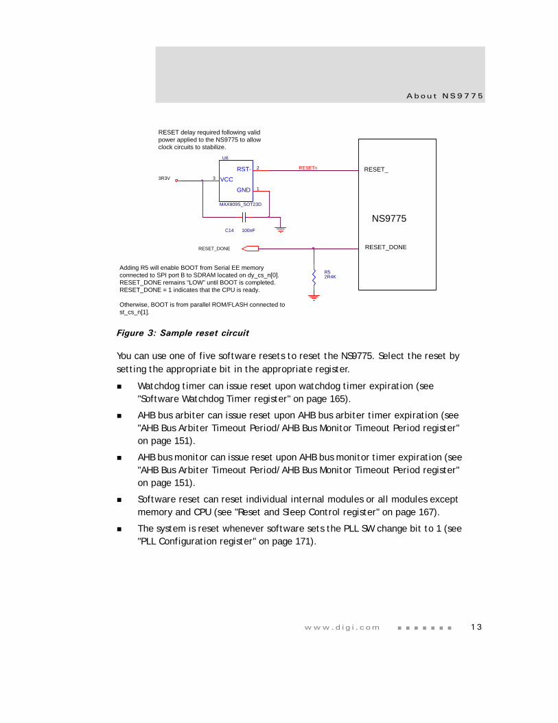
Figure 3 shows a sample reset circuit.
www.d i g i . com 13
Abou t NS9775
Figure 3: Sample reset circuit
You can use one of five software resets to reset the NS9775. Select the reset by setting the appropriate bit in the appropriate register.
Watchdog timer can issue reset upon watchdog timer expiration (see "Software Watchdog Timer register" on page 165).
AHB bus arbiter can issue reset upon AHB bus arbiter timer expiration (see "AHB Bus Arbiter Timeout Period/AHB Bus Monitor Timeout Period register" on page 151).
AHB bus monitor can issue reset upon AHB bus monitor timer expiration (see "AHB Bus Arbiter Timeout Period/AHB Bus Monitor Timeout Period register" on page 151).
Software reset can reset individual internal modules or all modules except memory and CPU (see "Reset and Sleep Control register" on page 167).
The system is reset whenever software sets the PLL SW change bit to 1 (see "PLL Configuration register" on page 171).
C14 100nF
Adding R5 will enable BOOT from Serial EE memoryconnected to SPI port B to SDRAM located on dy_cs_n[0].RESET_DONE remains “LOW” until BOOT is completed.RESET_DONE = 1 indicates that the CPU is ready.
Otherwise, BOOT is from parallel ROM/FLASH connected tost_cs_n[1].
RESET_
NS9775
RESET_DONE
RESETnRST-
VCC
GND
U6
MAX809S_SOT23D
2
3
1
R52R4K
3R3V
RESET_DONE
RESET delay required following validpower applied to the NS9775 to allowclock circuits to stabilize.
Sys t em c l o c k
1 4 NS9775 Ha r dwa r e Re f e r ence
Hardware reset duration is 4 ms for PLL to stabilize. Software duration depends on speed grade, as shown in Table 1.
The minimum reset pulse width is 10 crystal clocks.
System clock
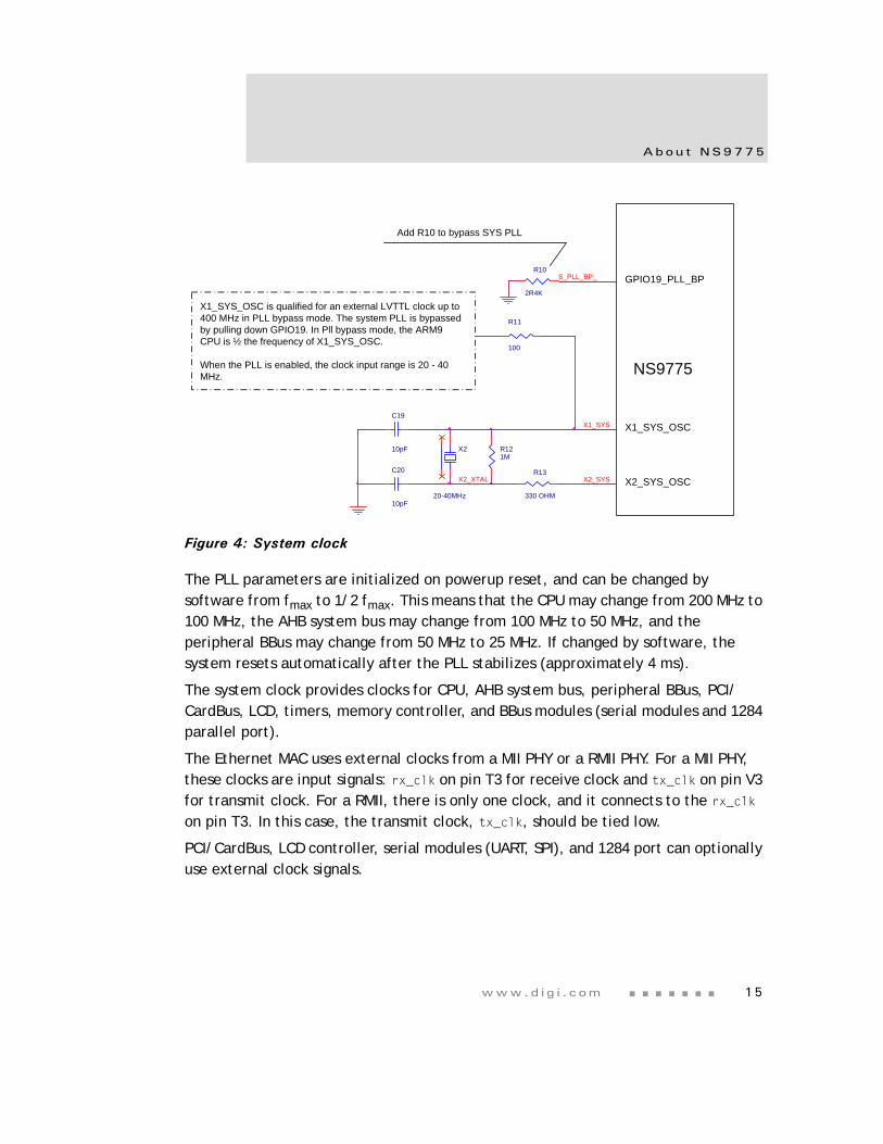
The system clock is provided to the NS9775 by either a crystal or an external oscillator. Table 2 shows sample clock frequency settings for each chip speed grade.
If an oscillator is used, it must be connected to the x1_sys_osc input (C8 pin) on the NS9775. If a crystal is used, it must be connected with a circuit such as the one shown in Figure 4.
Speed grade CPU clock cycles Duration
200 MHz 128 640 ns
Table 1: Software reset duration
Speed cpu_clk hclk (main bus) bbus_clk
200 MHz 200 (199.0656) 99.5328 49.7664
Table 2: Sample clock frequency settings with 29.4912 MHz crystal
www.d i g i . com 15
Abou t NS9775
Figure 4: System clock
The PLL parameters are initialized on powerup reset, and can be changed by software from fmax to 1/2 fmax. This means that the CPU may change from 200 MHz to 100 MHz, the AHB system bus may change from 100 MHz to 50 MHz, and the peripheral BBus may change from 50 MHz to 25 MHz. If changed by software, the system resets automatically after the PLL stabilizes (approximately 4 ms).
The system clock provides clocks for CPU, AHB system bus, peripheral BBus, PCI/CardBus, LCD, timers, memory controller, and BBus modules (serial modules and 1284 parallel port).
The Ethernet MAC uses external clocks from a MII PHY or a RMII PHY. For a MII PHY, these clocks are input signals: rx_clk on pin T3 for receive clock and tx_clk on pin V3 for transmit clock. For a RMII, there is only one clock, and it connects to the rx_clk on pin T3. In this case, the transmit clock, tx_clk, should be tied low.
PCI/CardBus, LCD controller, serial modules (UART, SPI), and 1284 port can optionally use external clock signals.
X1_SYS
GPIO19_PLL_BP
R121M
S_PLL_BP_
X2_SYS_OSC
X1_SYS_OSC is qualified for an external LVTTL clock up to400 MHz in PLL bypass mode. The system PLL is bypassedby pulling down GPIO19. In Pll bypass mode, the ARM9CPU is ½ the frequency of X1_SYS_OSC.
When the PLL is enabled, the clock input range is 20 - 40MHz.
Add R10 to bypass SYS PLL
X1_SYS_OSC
R10
2R4K
X2_XTAL
X2
20-40MHz
C19
10pF
R11
100
NS9775
R13
330 OHM
X2_SYSC20
10pF
P r i n t e r v i d eo c l o c k
1 6 NS9775 Ha r dwa r e Re f e r ence
Printer video clock
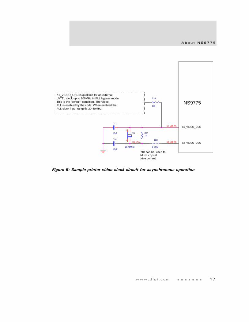
The printer video module allows the NS9775 to connect to several print engines, including monochrome, four-pass color, and one-pass tandem color print engines. The module can operate in synchronous and asynchronous modes.
The maximum clock rate for synchronous mode is 200 MHz. The maximum clock rate for asynchronous mode is 100 MHz.
In synchronous mode, the external system clock provides the clock that transmits the video bit stream to the print engine. There are four input video clock signals, with programmable active edges. Monochrome and four-pass color print engines use only one clock signal provided by the print engine. The default is the vclk_0 signal on pin R1. The tandem engines provide either all four clock signals (one per color plane) or one common video clock signal. When using only the single video clock signal from the print engine, the signal must be connected to all four NS9775 input video clock signals.
In asynchronous mode, the NS9775 provides the clock that transmits the video bit stream to the print engine. This clock can be generated by a dedicated internal video PLL and an external crystal, or by an external oscillator. In external oscillator mode, the PLL is bypassed (the default mode). The external oscillator provides the actual video clocks up to 200 MHz when using LV-PECL/LDVS logic. With the PLL enabled, the crystal oscillator range must be between 20 and 440 MHz. The appropriate frequency is selected by using the proper multiplier and divider factors in the PLL.
Figure 5 shows an example of a printer video clock circuit for asynchronous mode of operation. Figure 6 shows the print engine clock generator and the PLL setup table. All multiply and divide factors are programmable.
www.d i g i . com 17
Abou t NS9775
Figure 5: Sample printer video clock circuit for asynchronous operation
C28
10pF
NS9775R14
100
R171M
X1_VIDEO
X2_VIDEOX3_XTAL
X3
20-40MHz
X2_VIDEO_OSC
X1_VIDEO_OSC is qualified for an externalLVTTL clock up to 200MHz in PLL bypass mode.This is the "default" condition. The VideoPLL is enabled by the code. When enabled thePLL clock input range is 20-40MHz.
C27
10pF
R18
0 OHM
R18 can be used toadjust crystaldrive current
X1_VIDEO_OSC
USB c l o c k
1 8 NS9775 Ha r dwa r e Re f e r ence
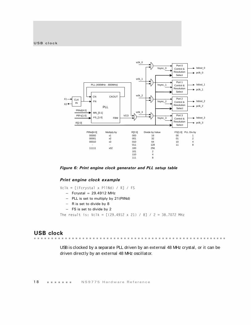
Figure 6: Print engine clock generator and PLL setup table
Print engine clock example
Vclk = [(Fcrystal x PllNd) / R] / FS
– Fcrystal = 29.4912 MHz – PLL is set to multiply by 21(PllNd)– R is set to divide by 8– FS is set to divide by 2
The result is: Vclk = [(29.4912 x 21) / 8] / 2 = 38.7072 MHz
USB clock
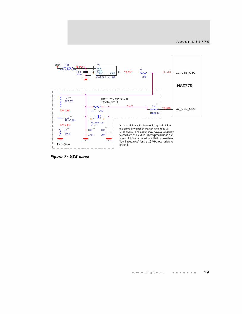
USB is clocked by a separate PLL driven by an external 48 MHz crystal, or it can be driven directly by an external 48 MHz oscillator.
Port 0Control &Resolution
Selectpclk_0
bdout_0hsync_0
Port 1Control &Resolution
Selectpclk_1
bdout_1hsync_1
Port 2Control &Resolution
Selectpclk_2
bdout_2hsync_2
Port 3Control &Resolution
Selectpclk_3
bdout_3hsync_3
R[2:0]
PllNd[4:0]
VCO
PllNd[4:0] Multiply by 00000 x1
00001 x2 00010 x3
- - 11111 x32
R[2:0] Divide by Value 000 16 001 32 010 64 011 128 100 256 101 2 110 4 111 8
vclk_0
vclk_1
vclk_3
vclk_2X1
X2
CLKIN
PllFs[1:0]
PLL
FBM
CKOUT
MN_[5:1]
FS_[1:0]
CN
FN
PLL (400MHz - 800MHz)
FS[1:0] PLL Div by 00 1 01 2 10 4 11 8
www.d i g i . com 19
Abou t NS9775
Figure 7: USB clock
Y1_PWR
**
**
Y1_OUT
**
TANK_LC
3R3V
C17
10pF
**
341
2
X148.0000MHz
C16100pF_5%
NS9775
L41uH_5%
TANK_RC
X2_USB_OSC
Y1
EC2600_TTS_48M
421 3
VCCGNDTEST OUT
R7
68R1
NOTE: ** = OPTIONAL Crystal circuit
C15
10pF
X1_IN
X1_USB_OSC
R8 1.5M
Tank Circuit
X1_USB
**
**
C9100nF
R9
100 OHM
**
X2_USB
R6
100
TB1
BEAD_0805_601
**X1 is a 48-MHz 3rd harmonic crystal. It hasthe same physical characteristics as a 16MHz crystal. The circuit may have a tendencyto oscillate at 16 MHz unless precautions aretaken. A LC-tank circuit is added to provide a“low impedance” for the 16 MHz oscillation toground.

21
NS9775 PinoutC H A P T E R 2
The NS9775 contains most of the major functional components for developing color printer or MFP controllers. All of the major I/Os required in a printer or MFP — Ethernet, USB (host and device), and IEEE 1284 — are provided on-chip. In addition, there are four serial interfaces, and a PCI interface that can be configured for CardBus compatibility. The NS9775 provides up to 50 general purpose I/O (GPIO) pins and configurable power management with sleep mode.
P i nou t a nd s i g na l d e s c r i p t i o n s
2 2 NS9775 Ha r dwa r e Re f e r ence
Pinout and signal descriptions
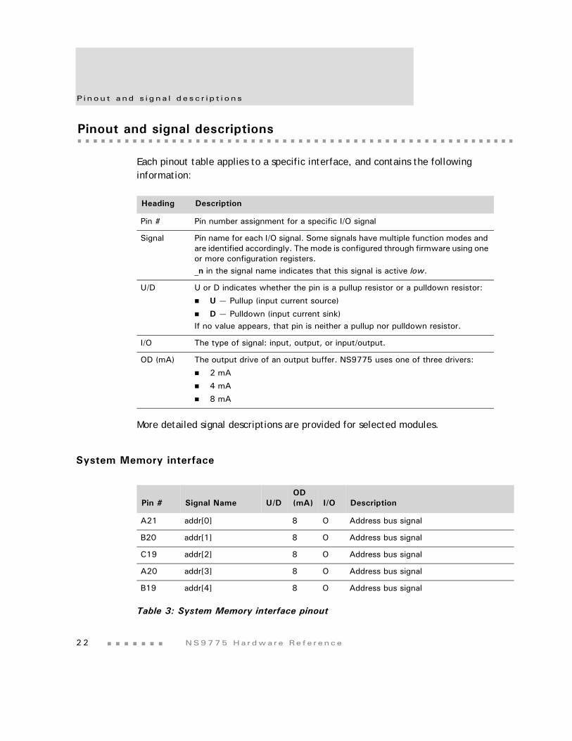
Each pinout table applies to a specific interface, and contains the following information:
More detailed signal descriptions are provided for selected modules.
System Memory interface
Heading Description
Pin # Pin number assignment for a specific I/O signal
Signal Pin name for each I/O signal. Some signals have multiple function modes and are identified accordingly. The mode is configured through firmware using one or more configuration registers. _n in the signal name indicates that this signal is active low.
U/D U or D indicates whether the pin is a pullup resistor or a pulldown resistor:
U — Pullup (input current source)
D — Pulldown (input current sink)If no value appears, that pin is neither a pullup nor pulldown resistor.
I/O The type of signal: input, output, or input/output.
OD (mA) The output drive of an output buffer. NS9775 uses one of three drivers:
2 mA
4 mA
8 mA
Pin # Signal Name U/DOD (mA) I/O Description
A21 addr[0] 8 O Address bus signal
B20 addr[1] 8 O Address bus signal
C19 addr[2] 8 O Address bus signal
A20 addr[3] 8 O Address bus signal
B19 addr[4] 8 O Address bus signal
Table 3: System Memory interface pinout
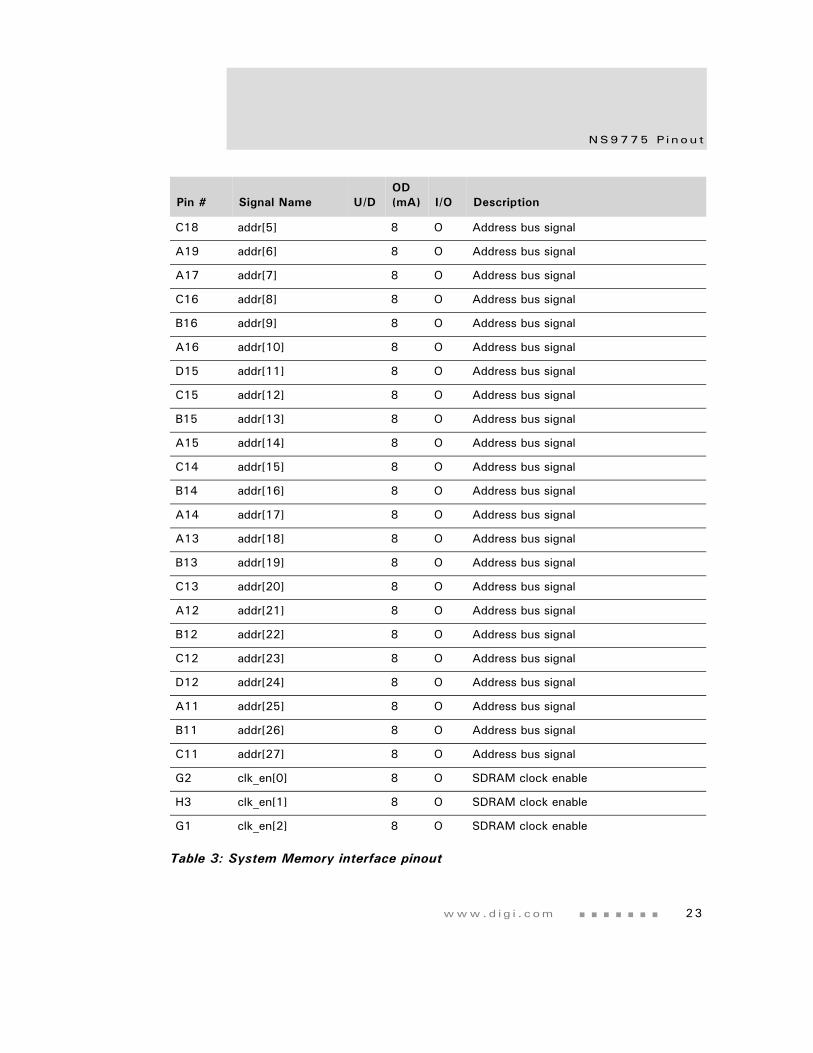
www.d i g i . com 23
NS9775 P i nou t
C18 addr[5] 8 O Address bus signal
A19 addr[6] 8 O Address bus signal
A17 addr[7] 8 O Address bus signal
C16 addr[8] 8 O Address bus signal
B16 addr[9] 8 O Address bus signal
A16 addr[10] 8 O Address bus signal
D15 addr[11] 8 O Address bus signal
C15 addr[12] 8 O Address bus signal
B15 addr[13] 8 O Address bus signal
A15 addr[14] 8 O Address bus signal
C14 addr[15] 8 O Address bus signal
B14 addr[16] 8 O Address bus signal
A14 addr[17] 8 O Address bus signal
A13 addr[18] 8 O Address bus signal
B13 addr[19] 8 O Address bus signal
C13 addr[20] 8 O Address bus signal
A12 addr[21] 8 O Address bus signal
B12 addr[22] 8 O Address bus signal
C12 addr[23] 8 O Address bus signal
D12 addr[24] 8 O Address bus signal
A11 addr[25] 8 O Address bus signal
B11 addr[26] 8 O Address bus signal
C11 addr[27] 8 O Address bus signal
G2 clk_en[0] 8 O SDRAM clock enable
H3 clk_en[1] 8 O SDRAM clock enable
G1 clk_en[2] 8 O SDRAM clock enable
Pin # Signal Name U/DOD (mA) I/O Description
Table 3: System Memory interface pinout
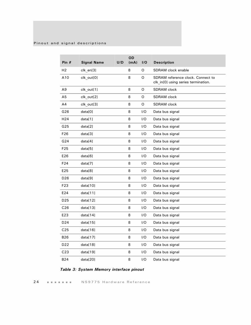
P i nou t a nd s i g na l d e s c r i p t i o n s
2 4 NS9775 Ha r dwa r e Re f e r ence
H2 clk_en[3] 8 O SDRAM clock enable
A10 clk_out[0] 8 O SDRAM reference clock. Connect to clk_in[0] using series termination.
A9 clk_out[1] 8 O SDRAM clock
A5 clk_out[2] 8 O SDRAM clock
A4 clk_out[3] 8 O SDRAM clock
G26 data[0] 8 I/O Data bus signal
H24 data[1] 8 I/O Data bus signal
G25 data[2] 8 I/O Data bus signal
F26 data[3] 8 I/O Data bus signal
G24 data[4] 8 I/O Data bus signal
F25 data[5] 8 I/O Data bus signal
E26 data[6] 8 I/O Data bus signal
F24 data[7] 8 I/O Data bus signal
E25 data[8] 8 I/O Data bus signal
D26 data[9] 8 I/O Data bus signal
F23 data[10] 8 I/O Data bus signal
E24 data[11] 8 I/O Data bus signal
D25 data[12] 8 I/O Data bus signal
C26 data[13] 8 I/O Data bus signal
E23 data[14] 8 I/O Data bus signal
D24 data[15] 8 I/O Data bus signal
C25 data[16] 8 I/O Data bus signal
B26 data[17] 8 I/O Data bus signal
D22 data[18] 8 I/O Data bus signal
C23 data[19] 8 I/O Data bus signal
B24 data[20] 8 I/O Data bus signal
Pin # Signal Name U/DOD (mA) I/O Description
Table 3: System Memory interface pinout
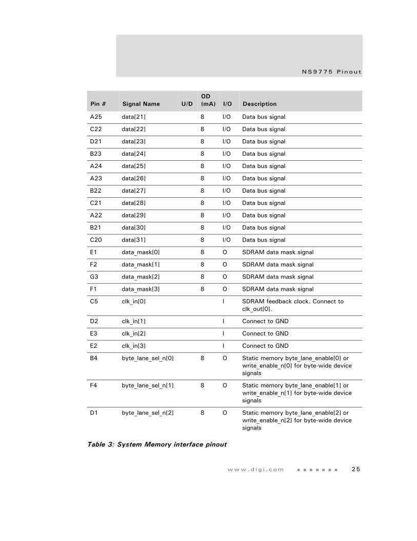
www.d i g i . com 25
NS9775 P i nou t
A25 data[21] 8 I/O Data bus signal
C22 data[22] 8 I/O Data bus signal
D21 data[23] 8 I/O Data bus signal
B23 data[24] 8 I/O Data bus signal
A24 data[25] 8 I/O Data bus signal
A23 data[26] 8 I/O Data bus signal
B22 data[27] 8 I/O Data bus signal
C21 data[28] 8 I/O Data bus signal
A22 data[29] 8 I/O Data bus signal
B21 data[30] 8 I/O Data bus signal
C20 data[31] 8 I/O Data bus signal
E1 data_mask[0] 8 O SDRAM data mask signal
F2 data_mask[1] 8 O SDRAM data mask signal
G3 data_mask[2] 8 O SDRAM data mask signal
F1 data_mask[3] 8 O SDRAM data mask signal
C5 clk_in[0] I SDRAM feedback clock. Connect to clk_out[0].
D2 clk_in[1] I Connect to GND
E3 clk_in[2] I Connect to GND
E2 clk_in[3] I Connect to GND
B4 byte_lane_sel_n[0] 8 O Static memory byte_lane_enable[0] or write_enable_n[0] for byte-wide device signals
F4 byte_lane_sel_n[1] 8 O Static memory byte_lane_enable[1] or write_enable_n[1] for byte-wide device signals
D1 byte_lane_sel_n[2] 8 O Static memory byte_lane_enable[2] or write_enable_n[2] for byte-wide device signals
Pin # Signal Name U/DOD (mA) I/O Description
Table 3: System Memory interface pinout
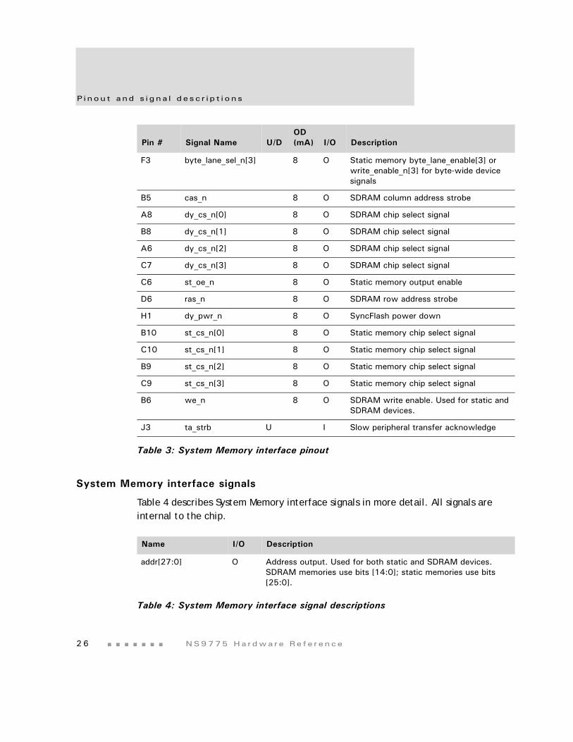
P i nou t a nd s i g na l d e s c r i p t i o n s
2 6 NS9775 Ha r dwa r e Re f e r ence
System Memory interface signals
Table 4 describes System Memory interface signals in more detail. All signals are internal to the chip.
F3 byte_lane_sel_n[3] 8 O Static memory byte_lane_enable[3] or write_enable_n[3] for byte-wide device signals
B5 cas_n 8 O SDRAM column address strobe
A8 dy_cs_n[0] 8 O SDRAM chip select signal
B8 dy_cs_n[1] 8 O SDRAM chip select signal
A6 dy_cs_n[2] 8 O SDRAM chip select signal
C7 dy_cs_n[3] 8 O SDRAM chip select signal
C6 st_oe_n 8 O Static memory output enable
D6 ras_n 8 O SDRAM row address strobe
H1 dy_pwr_n 8 O SyncFlash power down
B10 st_cs_n[0] 8 O Static memory chip select signal
C10 st_cs_n[1] 8 O Static memory chip select signal
B9 st_cs_n[2] 8 O Static memory chip select signal
C9 st_cs_n[3] 8 O Static memory chip select signal
B6 we_n 8 O SDRAM write enable. Used for static and SDRAM devices.
J3 ta_strb U I Slow peripheral transfer acknowledge
Pin # Signal Name U/DOD (mA) I/O Description
Table 3: System Memory interface pinout
Name I/O Description
addr[27:0] O Address output. Used for both static and SDRAM devices. SDRAM memories use bits [14:0]; static memories use bits [25:0].
Table 4: System Memory interface signal descriptions
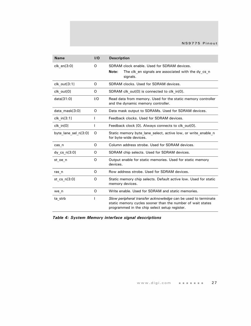
www.d i g i . com 27
NS9775 P i nou t
clk_en[3:0] O SDRAM clock enable. Used for SDRAM devices.
Note: The clk_en signals are associated with the dy_cs_n signals.
clk_out[3:1] O SDRAM clocks. Used for SDRAM devices.
clk_out[0] O SDRAM clk_out[0] is connected to clk_in[0].
data[31:0] I/O Read data from memory. Used for the static memory controller and the dynamic memory controller.
data_mask[3:0] O Data mask output to SDRAMs. Used for SDRAM devices.
clk_in[3:1] I Feedback clocks. Used for SDRAM devices.
clk_in[0] I Feedback clock [0]. Always connects to clk_out[0].
byte_lane_sel_n[3:0] O Static memory byte_lane_select, active low, or write_enable_n for byte-wide devices.
cas_n O Column address strobe. Used for SDRAM devices.
dy_cs_n[3:0] O SDRAM chip selects. Used for SDRAM devices.
st_oe_n O Output enable for static memories. Used for static memory devices.
ras_n O Row address strobe. Used for SDRAM devices.
st_cs_n[3:0] O Static memory chip selects. Default active low. Used for static memory devices.
we_n O Write enable. Used for SDRAM and static memories.
ta_strb I Slow peripheral transfer acknowledge can be used to terminate static memory cycles sooner than the number of wait states programmed in the chip select setup register.
Name I/O Description
Table 4: System Memory interface signal descriptions
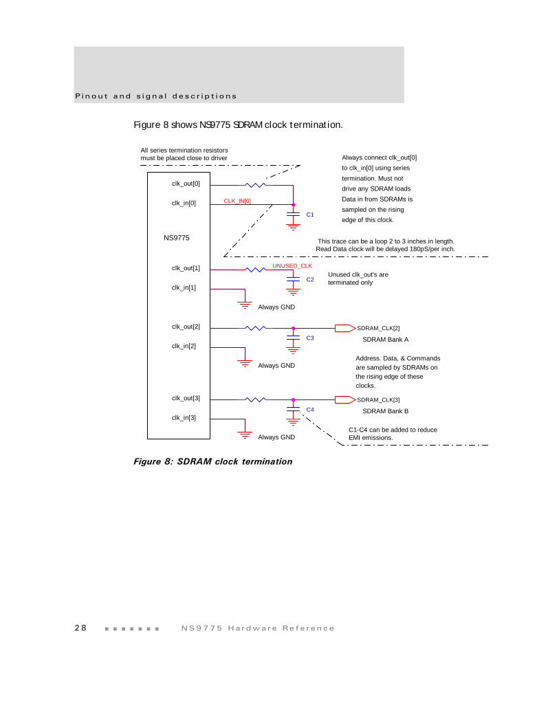
P i nou t a nd s i g na l d e s c r i p t i o n s
2 8 NS9775 Ha r dwa r e Re f e r ence
Figure 8 shows NS9775 SDRAM clock termination.
Figure 8: SDRAM clock termination
C1-C4 can be added to reduceEMI emissions.
SDRAM_CLK[2]
This trace can be a loop 2 to 3 inches in length.Read Data clock will be delayed 180pS/per inch.
clk_out[2]
C4
Always GND
SDRAM Bank B
C2
clk_in[0]
Address. Data, & Commandsare sampled by SDRAMs onthe rising edge of theseclocks.
clk_in[1]
SDRAM Bank AC3clk_in[2]
clk_in[3]
Always GND
clk_out[3]
NS9775
Unused clk_out's areterminated only
UNUSED_CLK
Always connect clk_out[0]to clk_in[0] using seriestermination. Must notdrive any SDRAM loadsData in from SDRAMs issampled on the risingedge of this clock.
CLK_IN[0]
clk_out[0]
All series termination resistorsmust be placed close to driver
clk_out[1]
SDRAM_CLK[3]
C1
Always GND
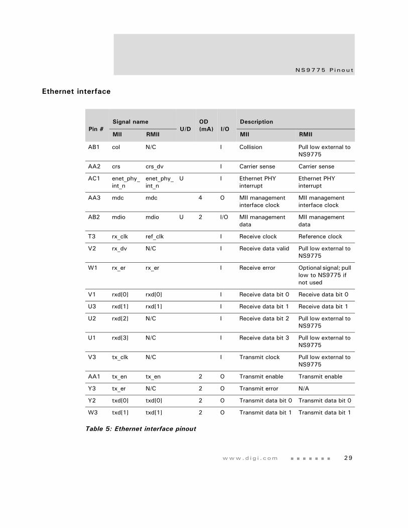
www.d i g i . com 29
NS9775 P i nou t
Ethernet interface
Pin #Signal name
U/DOD (mA) I/O
Description
MII RMII MII RMII
AB1 col N/C I Collision Pull low external to NS9775
AA2 crs crs_dv I Carrier sense Carrier sense
AC1 enet_phy_int_n
enet_phy_int_n
U I Ethernet PHY interrupt
Ethernet PHY interrupt
AA3 mdc mdc 4 O MII management interface clock
MII management interface clock
AB2 mdio mdio U 2 I/O MII management data
MII management data
T3 rx_clk ref_clk I Receive clock Reference clock
V2 rx_dv N/C I Receive data valid Pull low external to NS9775
W1 rx_er rx_er I Receive error Optional signal; pull low to NS9775 if not used
V1 rxd[0] rxd[0] I Receive data bit 0 Receive data bit 0
U3 rxd[1] rxd[1] I Receive data bit 1 Receive data bit 1
U2 rxd[2] N/C I Receive data bit 2 Pull low external to NS9775
U1 rxd[3] N/C I Receive data bit 3 Pull low external to NS9775
V3 tx_clk N/C I Transmit clock Pull low external to NS9775
AA1 tx_en tx_en 2 O Transmit enable Transmit enable
Y3 tx_er N/C 2 O Transmit error N/A
Y2 txd[0] txd[0] 2 O Transmit data bit 0 Transmit data bit 0
W3 txd[1] txd[1] 2 O Transmit data bit 1 Transmit data bit 1
Table 5: Ethernet interface pinout
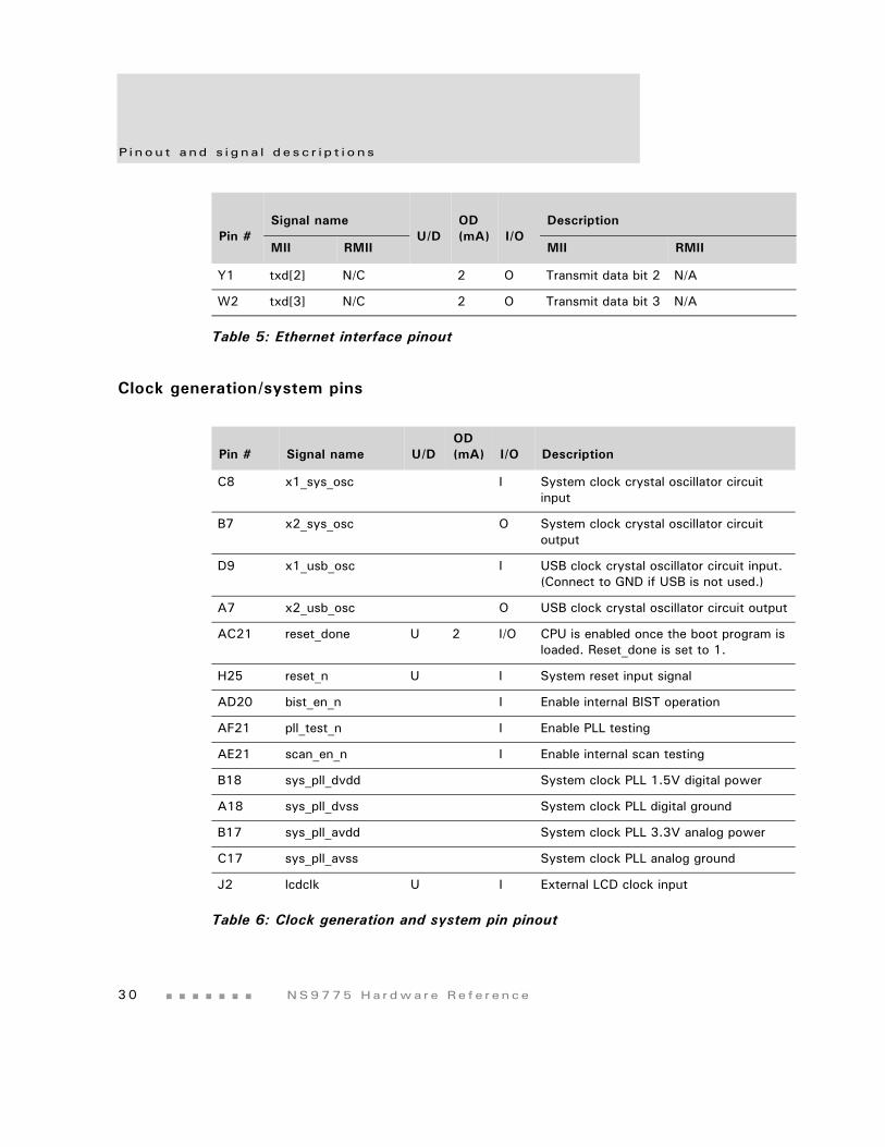
P i nou t a nd s i g na l d e s c r i p t i o n s
3 0 NS9775 Ha r dwa r e Re f e r ence
Clock generation/system pins
Y1 txd[2] N/C 2 O Transmit data bit 2 N/A
W2 txd[3] N/C 2 O Transmit data bit 3 N/A
Pin #Signal name
U/DOD (mA) I/O
Description
MII RMII MII RMII
Table 5: Ethernet interface pinout
Pin # Signal name U/DOD (mA) I/O Description
C8 x1_sys_osc I System clock crystal oscillator circuit input
B7 x2_sys_osc O System clock crystal oscillator circuit output
D9 x1_usb_osc I USB clock crystal oscillator circuit input. (Connect to GND if USB is not used.)
A7 x2_usb_osc O USB clock crystal oscillator circuit output
AC21 reset_done U 2 I/O CPU is enabled once the boot program is loaded. Reset_done is set to 1.
H25 reset_n U I System reset input signal
AD20 bist_en_n I Enable internal BIST operation
AF21 pll_test_n I Enable PLL testing
AE21 scan_en_n I Enable internal scan testing
B18 sys_pll_dvdd System clock PLL 1.5V digital power
A18 sys_pll_dvss System clock PLL digital ground
B17 sys_pll_avdd System clock PLL 3.3V analog power
C17 sys_pll_avss System clock PLL analog ground
J2 lcdclk U I External LCD clock input
Table 6: Clock generation and system pin pinout
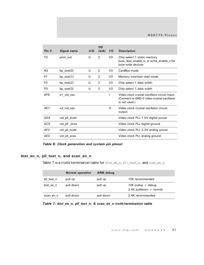
www.d i g i . com 31
NS9775 P i nou t
bist_en_n, pll_test_n, and scan_en_n
Table 7 is a truth/termination table for bist_en_n, pll_test_n, and scan_en_n.
T2 print_out U 2 I/O Chip select 1 static memory byte_lane_enable_n, or write_enable_n for byte-wide devices
N3 bp_stat[0] U 2 I/O CardBus mode
P1 bp_stat[1] U 2 I/O Memory interface read mode
P2 bp_stat[2] U 2 I/O Chip select 1 data width
P3 bp_stat[3] U 2 I/O Chip select 1 data width
AF6 x1_vid_osc I Video clock crystal oscillator circuit input. (Connect to GND if video crystal oscillator is not used.)
AE7 x2_vid_osc O Video clock crystal oscillator circuit output
AD4 vid_pll_dvdd Video clock PLL 1.5V digital power
AC5 vid_pll _dvss Video clock PLL digital ground
AF2 vid_pll_avdd Video clock PLL 3.3V analog power
AE3 vid_pll_avss Video clock PLL analog ground
Pin # Signal name U/DOD (mA) I/O Description
Table 6: Clock generation and system pin pinout
Normal operation ARM debug
pll_test_n pull up pull up 10K recommended
bist_en_n pull down pull up 10K pullup = debug2.4K pulldown = normal
scan_en_n pull down pull down 2.4K recommended
Table 7: bist_en_n, pll_test_n, & scan_en_n truth/termination table
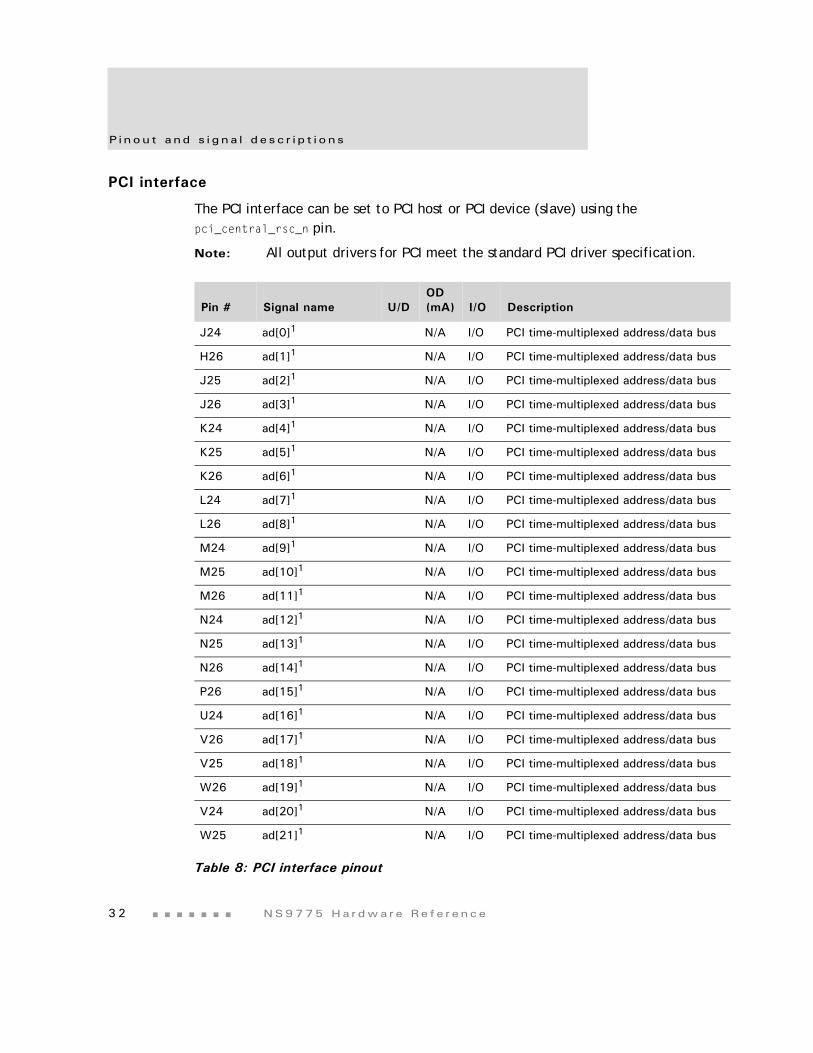
P i nou t a nd s i g na l d e s c r i p t i o n s
3 2 NS9775 Ha r dwa r e Re f e r ence
PCI interface
The PCI interface can be set to PCI host or PCI device (slave) using the pci_central_rsc_n pin.
Note: All output drivers for PCI meet the standard PCI driver specification.
Pin # Signal name U/DOD (mA) I/O Description
J24 ad[0]1 N/A I/O PCI time-multiplexed address/data bus
H26 ad[1]1 N/A I/O PCI time-multiplexed address/data bus
J25 ad[2]1 N/A I/O PCI time-multiplexed address/data bus
J26 ad[3]1 N/A I/O PCI time-multiplexed address/data bus
K24 ad[4]1 N/A I/O PCI time-multiplexed address/data bus
K25 ad[5]1 N/A I/O PCI time-multiplexed address/data bus
K26 ad[6]1 N/A I/O PCI time-multiplexed address/data bus
L24 ad[7]1 N/A I/O PCI time-multiplexed address/data bus
L26 ad[8]1 N/A I/O PCI time-multiplexed address/data bus
M24 ad[9]1 N/A I/O PCI time-multiplexed address/data bus
M25 ad[10]1 N/A I/O PCI time-multiplexed address/data bus
M26 ad[11]1 N/A I/O PCI time-multiplexed address/data bus
N24 ad[12]1 N/A I/O PCI time-multiplexed address/data bus
N25 ad[13]1 N/A I/O PCI time-multiplexed address/data bus
N26 ad[14]1 N/A I/O PCI time-multiplexed address/data bus
P26 ad[15]1 N/A I/O PCI time-multiplexed address/data bus
U24 ad[16]1 N/A I/O PCI time-multiplexed address/data bus
V26 ad[17]1 N/A I/O PCI time-multiplexed address/data bus
V25 ad[18]1 N/A I/O PCI time-multiplexed address/data bus
W26 ad[19]1 N/A I/O PCI time-multiplexed address/data bus
V24 ad[20]1 N/A I/O PCI time-multiplexed address/data bus
W25 ad[21]1 N/A I/O PCI time-multiplexed address/data bus
Table 8: PCI interface pinout
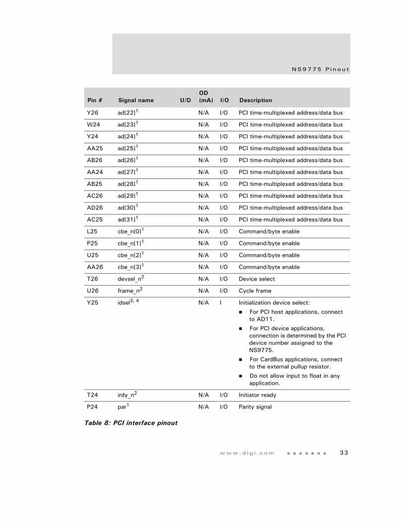
www.d i g i . com 33
NS9775 P i nou t
Y26 ad[22]1 N/A I/O PCI time-multiplexed address/data bus
W24 ad[23]1 N/A I/O PCI time-multiplexed address/data bus
Y24 ad[24]1 N/A I/O PCI time-multiplexed address/data bus
AA25 ad[25]1 N/A I/O PCI time-multiplexed address/data bus
AB26 ad[26]1 N/A I/O PCI time-multiplexed address/data bus
AA24 ad[27]1 N/A I/O PCI time-multiplexed address/data bus
AB25 ad[28]1 N/A I/O PCI time-multiplexed address/data bus
AC26 ad[29]1 N/A I/O PCI time-multiplexed address/data bus
AD26 ad[30]1 N/A I/O PCI time-multiplexed address/data bus
AC25 ad[31]1 N/A I/O PCI time-multiplexed address/data bus
L25 cbe_n[0]1 N/A I/O Command/byte enable
P25 cbe_n[1]1 N/A I/O Command/byte enable
U25 cbe_n[2]1 N/A I/O Command/byte enable
AA26 cbe_n[3]1 N/A I/O Command/byte enable
T26 devsel_n2 N/A I/O Device select
U26 frame_n2 N/A I/O Cycle frame
Y25 idsel3, 4 N/A I Initialization device select:
For PCI host applications, connect to AD11.
For PCI device applications, connection is determined by the PCI device number assigned to the NS9775.
For CardBus applications, connect to the external pullup resistor.
Do not allow input to float in any application.
T24 irdy_n2 N/A I/O Initiator ready
P24 par1 N/A I/O Parity signal
Pin # Signal name U/DOD (mA) I/O Description
Table 8: PCI interface pinout
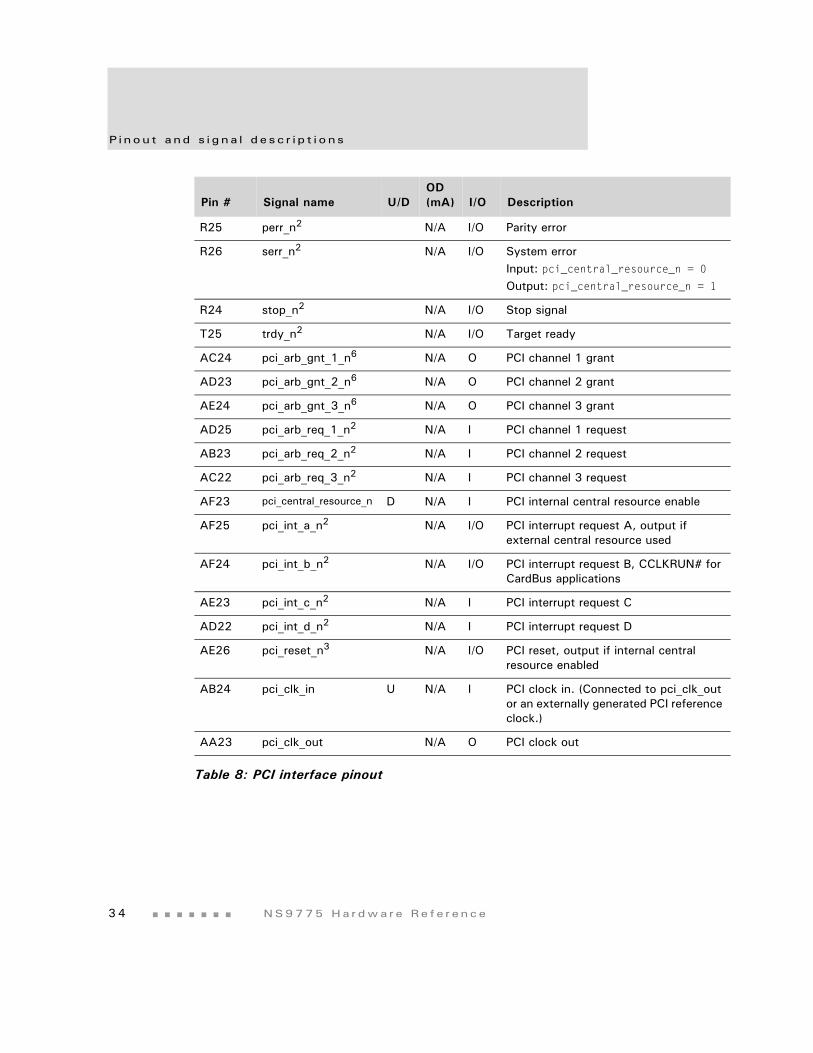
P i nou t a nd s i g na l d e s c r i p t i o n s
3 4 NS9775 Ha r dwa r e Re f e r ence
R25 perr_n2 N/A I/O Parity error
R26 serr_n2 N/A I/O System errorInput: pci_central_resource_n = 0Output: pci_central_resource_n = 1
R24 stop_n2 N/A I/O Stop signal
T25 trdy_n2 N/A I/O Target ready
AC24 pci_arb_gnt_1_n6 N/A O PCI channel 1 grant
AD23 pci_arb_gnt_2_n6 N/A O PCI channel 2 grant
AE24 pci_arb_gnt_3_n6 N/A O PCI channel 3 grant
AD25 pci_arb_req_1_n2 N/A I PCI channel 1 request
AB23 pci_arb_req_2_n2 N/A I PCI channel 2 request
AC22 pci_arb_req_3_n2 N/A I PCI channel 3 request
AF23 pci_central_resource_n D N/A I PCI internal central resource enable
AF25 pci_int_a_n2 N/A I/O PCI interrupt request A, output if external central resource used
AF24 pci_int_b_n2 N/A I/O PCI interrupt request B, CCLKRUN# for CardBus applications
AE23 pci_int_c_n2 N/A I PCI interrupt request C
AD22 pci_int_d_n2 N/A I PCI interrupt request D
AE26 pci_reset_n3 N/A I/O PCI reset, output if internal central resource enabled
AB24 pci_clk_in U N/A I PCI clock in. (Connected to pci_clk_out or an externally generated PCI reference clock.)
AA23 pci_clk_out N/A O PCI clock out
Pin # Signal name U/DOD (mA) I/O Description
Table 8: PCI interface pinout
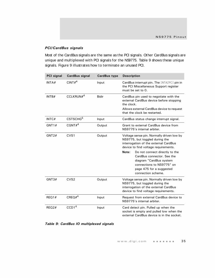
www.d i g i . com 35
NS9775 P i nou t
PCI/CardBus signals
Most of the CardBus signals are the same as the PCI signals. Other CardBus signals are unique and multiplexed with PCI signals for the NS9775. Table 9 shows these unique signals. Figure 9 illustrates how to terminate an unused PCI.
PCI signal CardBus signal CardBus type Description
INTA# CINT#4 Input CardBus interrupt pin. The INTA2PCI pin in the PCI Miscellaneous Support register must be set to 0.
INTB# CCLKRUN#4 Bidir CardBus pin used to negotiate with the external CardBus device before stopping the clock.Allows external CardBus device to request that the clock be restarted.
INTC# CSTSCHG5 Input CardBus status change interrupt signal.
GNT1# CGNT#4 Output Grant to external CardBus device from NS9775’s internal arbiter.
GNT2# CVS1 Output Voltage sense pin. Normally driven low by NS9775, but toggled during the interrogation of the external CardBus device to find voltage requirements.
Note: Do not connect directly to the CardBus connector. See the diagram "CardBus system connections to NS9775" on page 475 for a suggested connection scheme.
GNT3# CVS2 Output Voltage sense pin. Normally driven low by NS9775, but toggled during the interrogation of the external CardBus device to find voltage requirements.
REQ1# CREQ#4 Input Request from external CardBus device to NS9775’s internal arbiter.
REQ2# CCD14 Input Card detect pin. Pulled up when the socket is empty and pulled low when the external CardBus device is in the socket.
Table 9: CardBus IO multiplexed signals
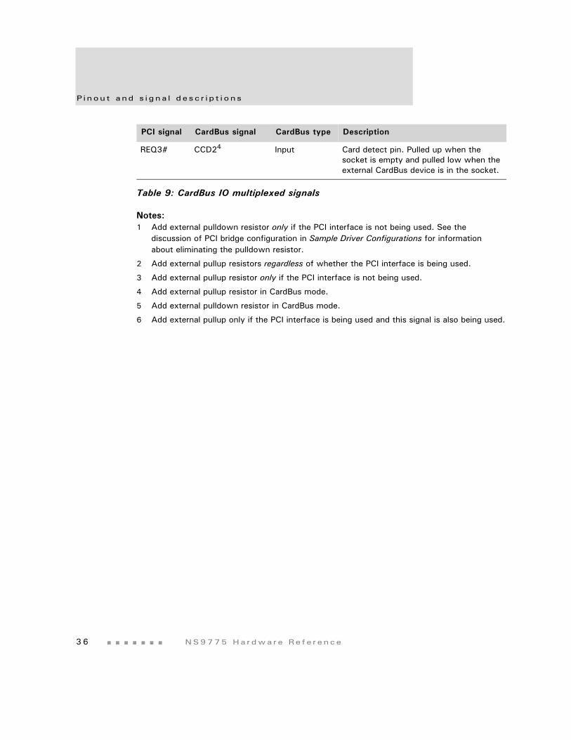
P i nou t a nd s i g na l d e s c r i p t i o n s
3 6 NS9775 Ha r dwa r e Re f e r ence
Notes:1 Add external pulldown resistor only if the PCI interface is not being used. See the
discussion of PCI bridge configuration in Sample Driver Configurations for information about eliminating the pulldown resistor.
2 Add external pullup resistors regardless of whether the PCI interface is being used.
3 Add external pullup resistor only if the PCI interface is not being used.
4 Add external pullup resistor in CardBus mode.
5 Add external pulldown resistor in CardBus mode.
6 Add external pullup only if the PCI interface is being used and this signal is also being used.
REQ3# CCD24 Input Card detect pin. Pulled up when the socket is empty and pulled low when the external CardBus device is in the socket.
PCI signal CardBus signal CardBus type Description
Table 9: CardBus IO multiplexed signals
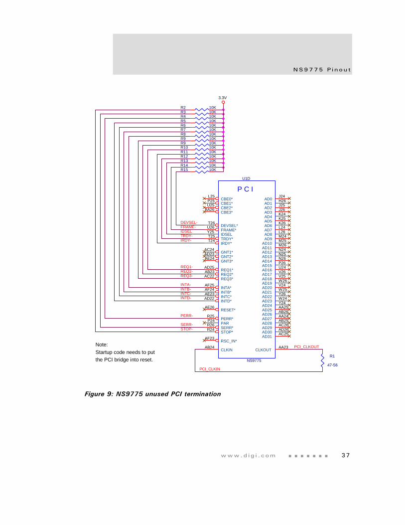
www.d i g i . com 37
NS9775 P i nou t
Figure 9: NS9775 unused PCI termination
INTA-
R3 10K
PCI_CLKIN
R2 10K
REQ3-
PERR-
FRAME-
INTC-
R1
47-56
R7 10K
IDSEL
REQ1-
R4 10K
R9 10K
STOP-
P C IU1D
NS9775
J24H26J25J26K24K25K26L24L26M24M25M26N24N25N26P26U24V26V25W26V24W25Y26W24Y24AA25AB26AA24AB25AC26AD26AC25
L25P25U25
AA26
T26U26Y25T25T24
AC24AD23AE24
AD25AB23AC22
AF25AF24AE23AD22
AE26
AB24 AA23
R25P24R26R24
AF23
AD0AD1AD2AD3AD4AD5AD6AD7AD8AD9
AD10AD11AD12AD13AD14AD15AD16AD17AD18AD19AD20AD21AD22AD23AD24AD25AD26AD27AD28AD29AD30AD31
CBE0*CBE1*CBE2*CBE3*
DEVSEL*FRAME*IDSELTRDY*IRDY*
GNT1*GNT2*GNT3*
REQ1*REQ2*REQ3*
INTA*INTB*INTC*INTD*
RESET*
CLKIN CLKOUT
PERR*PARSERR*STOP*
RSC_IN*Note:Startup code needs to putthe PCI bridge into reset.
R14 10K
R11 10K
R15 10K
INTB-
INTD-
3.3V
R12 10K
DEVSEL-
R6 10K
R13 10K
R5 10K
IRDY-
REQ2-
PCI_CLKOUT
TRDY-
SERR-
R10 10K
R8 10KR9 10K
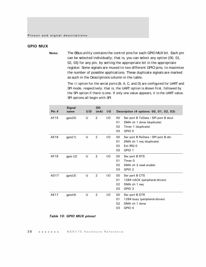
P i nou t a nd s i g na l d e s c r i p t i o n s
3 8 NS9775 Ha r dwa r e Re f e r ence
GPIO MUX
Note: The BBus utility contains the control pins for each GPIO MUX bit. Each pin can be selected individually; that is, you can select any option (00, 01, 02, 03) for any pin, by setting the appropriate bit in the appropriate register. Some signals are muxed to two different GPIO pins, to maximize the number of possible applications. These duplicate signals are marked as such in the Descriptions column in the table.
The 00 option for the serial ports (B, A, C, and D) are configured for UART and SPI mode, respectively; that is, the UART option is shown first, followed by the SPI option if there is one. If only one value appears, it is the UART value. SPI options all begin with SPI.
Pin #Signal name U/D
OD (mA) I/O Description (4 options: 00, 01, 02, 03)
AF19 gpio[0] U 2 I/O 00 Ser port B TxData / SPI port B dout01 DMA ch 1 done (duplicate)02 Timer 1 (duplicate)03 GPIO 0
AE18 gpio[1] U 2 I/O 00 Ser port B RxData / SPI port B din01 DMA ch 1 req (duplicate)02 Ext IRQ 003 GPIO 1
AF18 gpio [2] U 2 I/O 00 Ser port B RTS01 Timer 002 DMA ch 2 read enable03 GPIO 2
AD17 gpio[3] U 2 I/O 00 Ser port B CTS01 1284 nACK (peripheral-driven)02 DMA ch 1 req03 GPIO 3
AE17 gpio[4] U 2 I/O 00 Ser port B DTR01 1284 busy (peripheral-driven)02 DMA ch 1 done03 GPIO 4
Table 10: GPIO MUX pinout
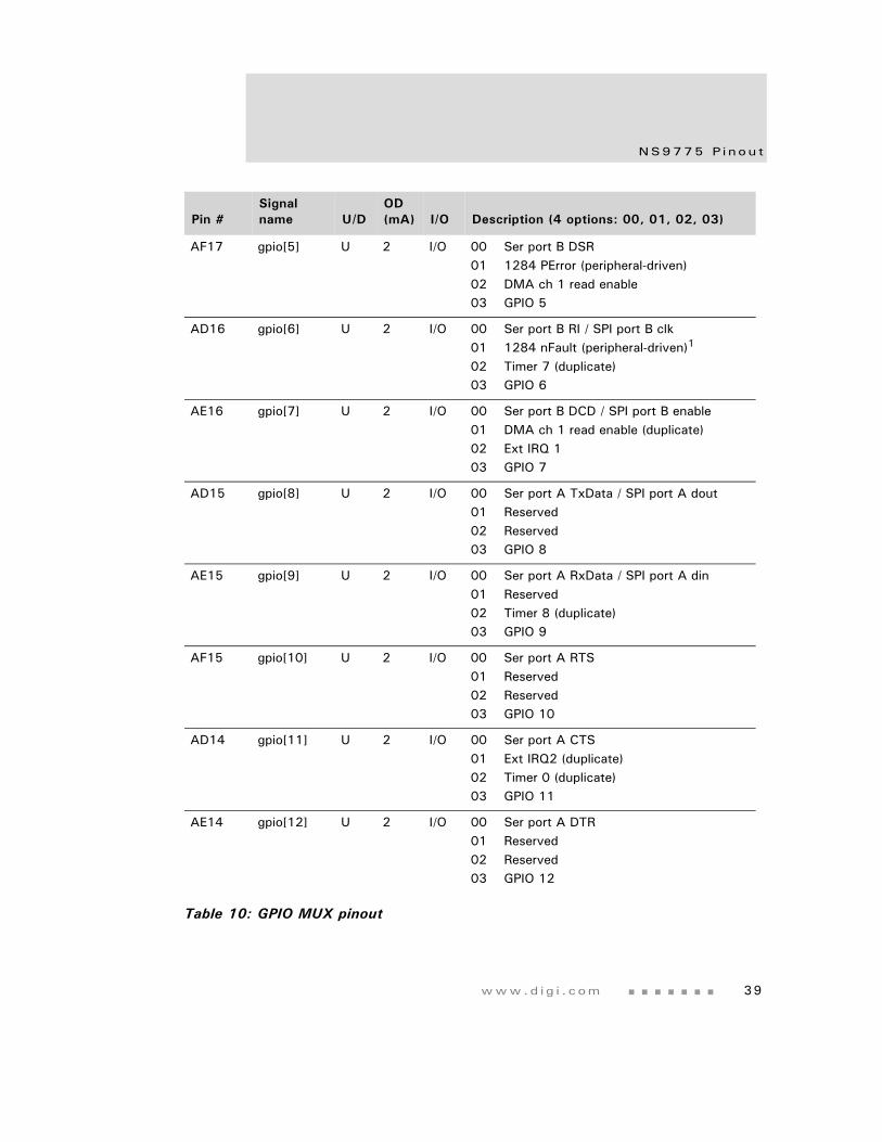
www.d i g i . com 39
NS9775 P i nou t
AF17 gpio[5] U 2 I/O 00 Ser port B DSR01 1284 PError (peripheral-driven)02 DMA ch 1 read enable03 GPIO 5
AD16 gpio[6] U 2 I/O 00 Ser port B RI / SPI port B clk01 1284 nFault (peripheral-driven)1
02 Timer 7 (duplicate)03 GPIO 6
AE16 gpio[7] U 2 I/O 00 Ser port B DCD / SPI port B enable01 DMA ch 1 read enable (duplicate)02 Ext IRQ 103 GPIO 7
AD15 gpio[8] U 2 I/O 00 Ser port A TxData / SPI port A dout01 Reserved02 Reserved03 GPIO 8
AE15 gpio[9] U 2 I/O 00 Ser port A RxData / SPI port A din01 Reserved02 Timer 8 (duplicate)03 GPIO 9
AF15 gpio[10] U 2 I/O 00 Ser port A RTS01 Reserved02 Reserved03 GPIO 10
AD14 gpio[11] U 2 I/O 00 Ser port A CTS01 Ext IRQ2 (duplicate)02 Timer 0 (duplicate)03 GPIO 11
AE14 gpio[12] U 2 I/O 00 Ser port A DTR01 Reserved02 Reserved03 GPIO 12
Pin #Signal name U/D
OD (mA) I/O Description (4 options: 00, 01, 02, 03)
Table 10: GPIO MUX pinout
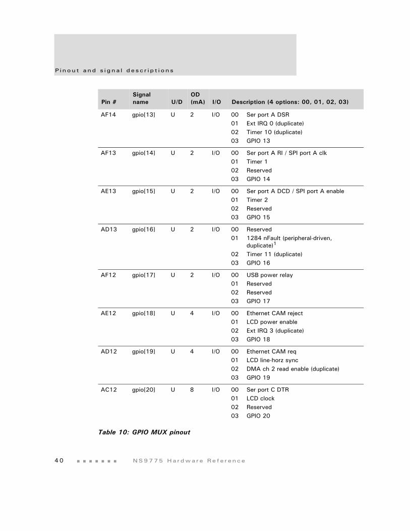
P i nou t a nd s i g na l d e s c r i p t i o n s
4 0 NS9775 Ha r dwa r e Re f e r ence
AF14 gpio[13] U 2 I/O 00 Ser port A DSR01 Ext IRQ 0 (duplicate)02 Timer 10 (duplicate)03 GPIO 13
AF13 gpio[14] U 2 I/O 00 Ser port A RI / SPI port A clk01 Timer 102 Reserved03 GPIO 14
AE13 gpio[15] U 2 I/O 00 Ser port A DCD / SPI port A enable01 Timer 202 Reserved03 GPIO 15
AD13 gpio[16] U 2 I/O 00 Reserved01 1284 nFault (peripheral-driven,
duplicate)1
02 Timer 11 (duplicate)03 GPIO 16
AF12 gpio[17] U 2 I/O 00 USB power relay01 Reserved02 Reserved03 GPIO 17
AE12 gpio[18] U 4 I/O 00 Ethernet CAM reject01 LCD power enable02 Ext IRQ 3 (duplicate)03 GPIO 18
AD12 gpio[19] U 4 I/O 00 Ethernet CAM req01 LCD line-horz sync02 DMA ch 2 read enable (duplicate)03 GPIO 19
AC12 gpio[20] U 8 I/O 00 Ser port C DTR01 LCD clock02 Reserved03 GPIO 20
Pin #Signal name U/D
OD (mA) I/O Description (4 options: 00, 01, 02, 03)
Table 10: GPIO MUX pinout
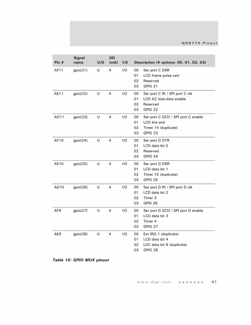
www.d i g i . com 41
NS9775 P i nou t
AF11 gpio[21] U 4 I/O 00 Ser port C DSR01 LCD frame pulse-vert02 Reserved03 GPIO 21
AE11 gpio[22] U 4 I/O 00 Ser port C RI / SPI port C clk01 LCD AC bias-data enable02 Reserved03 GPIO 22
AD11 gpio[23] U 4 I/O 00 Ser port C DCD / SPI port C enable01 LCD line end02 Timer 14 (duplicate)03 GPIO 23
AF10 gpio[24] U 4 I/O 00 Ser port D DTR01 LCD data bit 002 Reserved03 GPIO 24
AE10 gpio[25] U 4 I/O 00 Ser port D DSR01 LCD data bit 102 Timer 15 (duplicate)03 GPIO 25
AD10 gpio[26] U 4 I/O 00 Ser port D RI / SPI port D clk01 LCD data bit 202 Timer 303 GPI0 26
AF9 gpio[27] U 4 I/O 00 Ser port D DCD / SPI port D enable01 LCD data bit 302 Timer 403 GPIO 27
AE9 gpio[28] U 4 I/O 00 Ext IRQ 1 (duplicate)01 LCD data bit 402 LDC data bit 8 (duplicate)03 GPIO 28
Pin #Signal name U/D
OD (mA) I/O Description (4 options: 00, 01, 02, 03)
Table 10: GPIO MUX pinout
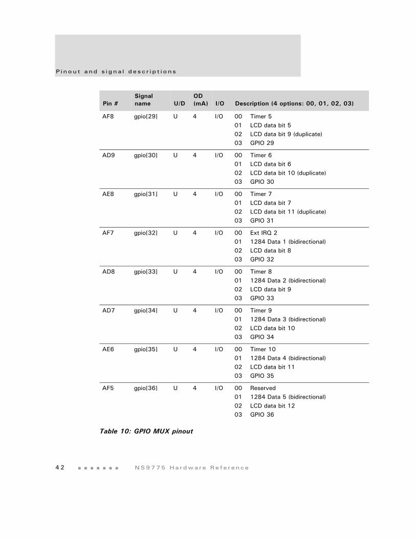
P i nou t a nd s i g na l d e s c r i p t i o n s
4 2 NS9775 Ha r dwa r e Re f e r ence
AF8 gpio[29] U 4 I/O 00 Timer 501 LCD data bit 502 LCD data bit 9 (duplicate)03 GPIO 29
AD9 gpio[30] U 4 I/O 00 Timer 601 LCD data bit 602 LCD data bit 10 (duplicate)03 GPIO 30
AE8 gpio[31] U 4 I/O 00 Timer 701 LCD data bit 702 LCD data bit 11 (duplicate)03 GPIO 31
AF7 gpio[32] U 4 I/O 00 Ext IRQ 201 1284 Data 1 (bidirectional)02 LCD data bit 803 GPIO 32
AD8 gpio[33] U 4 I/O 00 Timer 801 1284 Data 2 (bidirectional)02 LCD data bit 903 GPIO 33
AD7 gpio[34] U 4 I/O 00 Timer 901 1284 Data 3 (bidirectional)02 LCD data bit 1003 GPIO 34
AE6 gpio[35] U 4 I/O 00 Timer 1001 1284 Data 4 (bidirectional)02 LCD data bit 1103 GPIO 35
AF5 gpio[36] U 4 I/O 00 Reserved01 1284 Data 5 (bidirectional)02 LCD data bit 1203 GPIO 36
Pin #Signal name U/D
OD (mA) I/O Description (4 options: 00, 01, 02, 03)
Table 10: GPIO MUX pinout
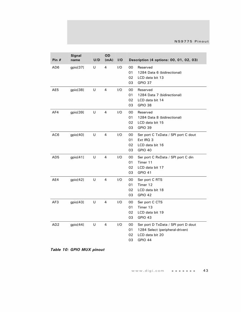
www.d i g i . com 43
NS9775 P i nou t
AD6 gpio[37] U 4 I/O 00 Reserved01 1284 Data 6 (bidirectional)02 LCD data bit 1303 GPIO 37
AE5 gpio[38] U 4 I/O 00 Reserved01 1284 Data 7 (bidirectional)02 LCD data bit 1403 GPIO 38
AF4 gpio[39] U 4 I/O 00 Reserved01 1284 Data 8 (bidirectional)02 LCD data bit 1503 GPIO 39
AC6 gpio[40] U 4 I/O 00 Ser port C TxData / SPI port C dout01 Ext IRQ 302 LCD data bit 1603 GPIO 40
AD5 gpio[41] U 4 I/O 00 Ser port C RxData / SPI port C din01 Timer 1102 LCD data bit 1703 GPIO 41
AE4 gpio[42] U 4 I/O 00 Ser port C RTS01 Timer 1202 LCD data bit 1803 GPIO 42
AF3 gpio[43] U 4 I/O 00 Ser port C CTS01 Timer 1302 LCD data bit 1903 GPIO 43
AD2 gpio[44] U 4 I/O 00 Ser port D TxData / SPI port D dout01 1284 Select (peripheral-driven)02 LCD data bit 2003 GPIO 44
Pin #Signal name U/D
OD (mA) I/O Description (4 options: 00, 01, 02, 03)
Table 10: GPIO MUX pinout
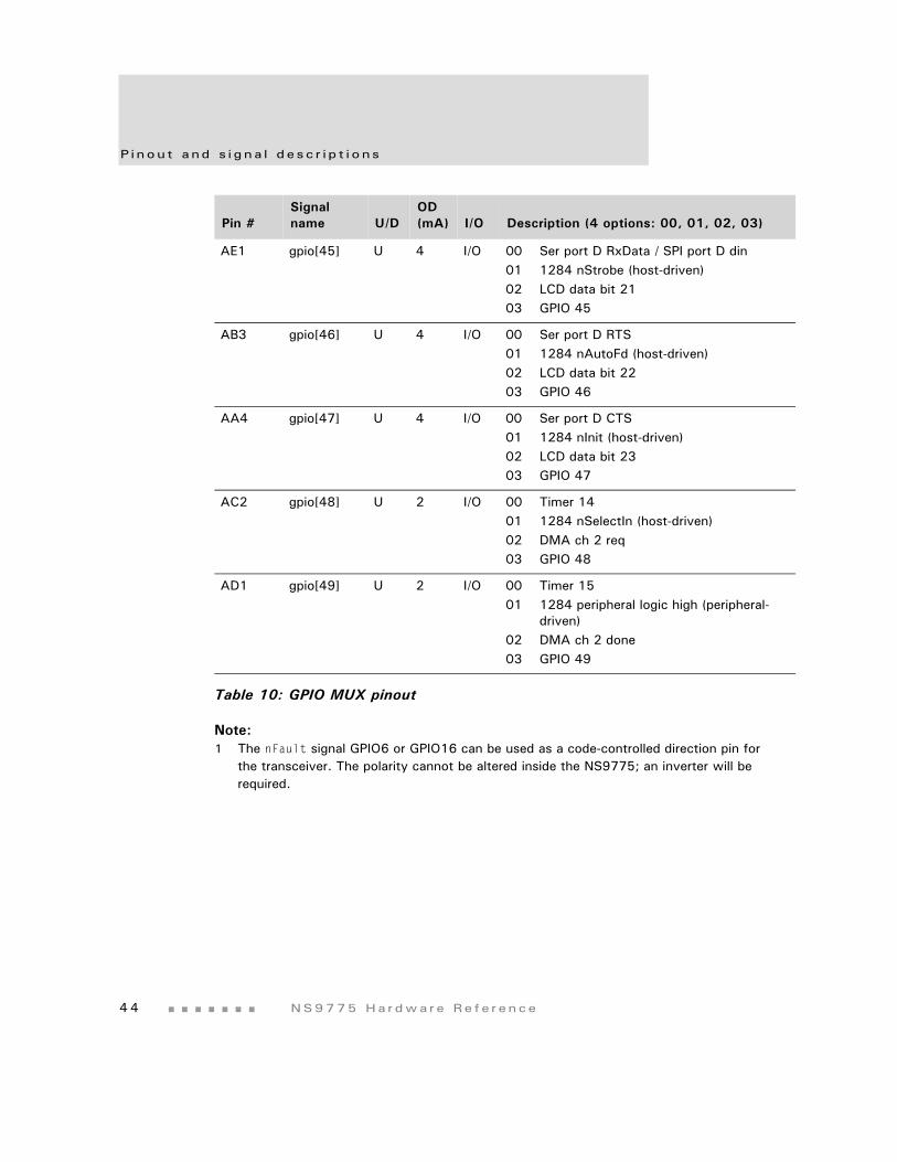
P i nou t a nd s i g na l d e s c r i p t i o n s
4 4 NS9775 Ha r dwa r e Re f e r ence
Note:1 The nFault signal GPIO6 or GPIO16 can be used as a code-controlled direction pin for
the transceiver. The polarity cannot be altered inside the NS9775; an inverter will be required.
AE1 gpio[45] U 4 I/O 00 Ser port D RxData / SPI port D din01 1284 nStrobe (host-driven)02 LCD data bit 2103 GPIO 45
AB3 gpio[46] U 4 I/O 00 Ser port D RTS01 1284 nAutoFd (host-driven)02 LCD data bit 2203 GPIO 46
AA4 gpio[47] U 4 I/O 00 Ser port D CTS01 1284 nInit (host-driven)02 LCD data bit 2303 GPIO 47
AC2 gpio[48] U 2 I/O 00 Timer 1401 1284 nSelectIn (host-driven)02 DMA ch 2 req03 GPIO 48
AD1 gpio[49] U 2 I/O 00 Timer 1501 1284 peripheral logic high (peripheral-
driven)02 DMA ch 2 done03 GPIO 49
Pin #Signal name U/D
OD (mA) I/O Description (4 options: 00, 01, 02, 03)
Table 10: GPIO MUX pinout
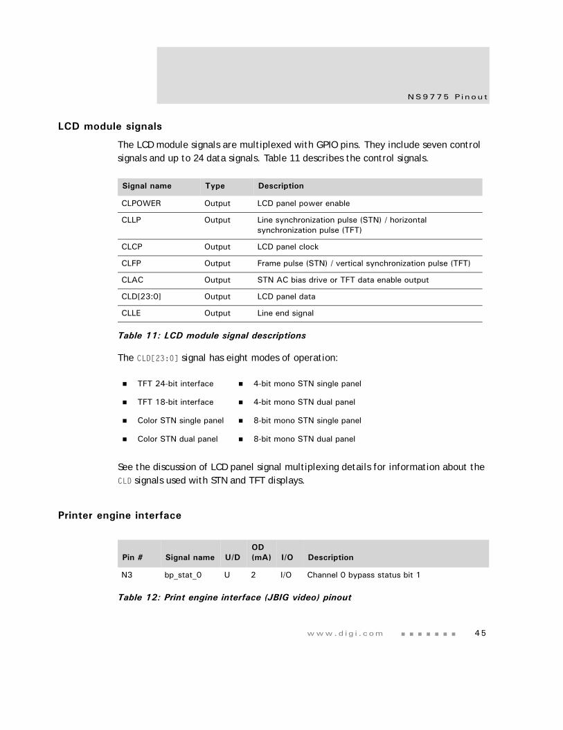
www.d i g i . com 45
NS9775 P i nou t
LCD module signals
The LCD module signals are multiplexed with GPIO pins. They include seven control signals and up to 24 data signals. Table 11 describes the control signals.
The CLD[23:0] signal has eight modes of operation:
See the discussion of LCD panel signal multiplexing details for information about the CLD signals used with STN and TFT displays.
Printer engine interface
Signal name Type Description
CLPOWER Output LCD panel power enable
CLLP Output Line synchronization pulse (STN) / horizontal synchronization pulse (TFT)
CLCP Output LCD panel clock
CLFP Output Frame pulse (STN) / vertical synchronization pulse (TFT)
CLAC Output STN AC bias drive or TFT data enable output
CLD[23:0] Output LCD panel data
CLLE Output Line end signal
Table 11: LCD module signal descriptions
TFT 24-bit interface 4-bit mono STN single panel
TFT 18-bit interface 4-bit mono STN dual panel
Color STN single panel 8-bit mono STN single panel
Color STN dual panel 8-bit mono STN dual panel
Pin # Signal name U/DOD (mA) I/O Description
N3 bp_stat_0 U 2 I/O Channel 0 bypass status bit 1
Table 12: Print engine interface (JBIG video) pinout
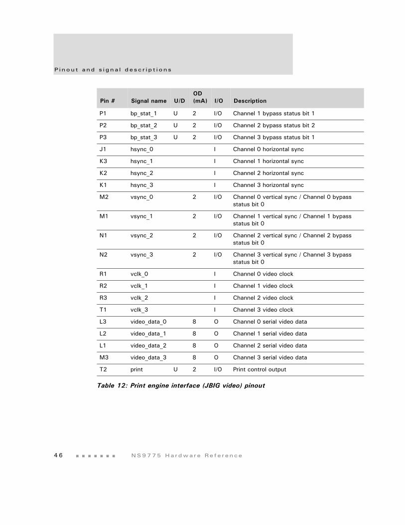
P i nou t a nd s i g na l d e s c r i p t i o n s
4 6 NS9775 Ha r dwa r e Re f e r ence
P1 bp_stat_1 U 2 I/O Channel 1 bypass status bit 1
P2 bp_stat_2 U 2 I/O Channel 2 bypass status bit 2
P3 bp_stat_3 U 2 I/O Channel 3 bypass status bit 1
J1 hsync_0 I Channel 0 horizontal sync
K3 hsync_1 I Channel 1 horizontal sync
K2 hsync_2 I Channel 2 horizontal sync
K1 hsync_3 I Channel 3 horizontal sync
M2 vsync_0 2 I/O Channel 0 vertical sync / Channel 0 bypass status bit 0
M1 vsync_1 2 I/O Channel 1 vertical sync / Channel 1 bypass status bit 0
N1 vsync_2 2 I/O Channel 2 vertical sync / Channel 2 bypass status bit 0
N2 vsync_3 2 I/O Channel 3 vertical sync / Channel 3 bypass status bit 0
R1 vclk_0 I Channel 0 video clock
R2 vclk_1 I Channel 1 video clock
R3 vclk_2 I Channel 2 video clock
T1 vclk_3 I Channel 3 video clock
L3 video_data_0 8 O Channel 0 serial video data
L2 video_data_1 8 O Channel 1 serial video data
L1 video_data_2 8 O Channel 2 serial video data
M3 video_data_3 8 O Channel 3 serial video data
T2 print U 2 I/O Print control output
Pin # Signal name U/DOD (mA) I/O Description
Table 12: Print engine interface (JBIG video) pinout
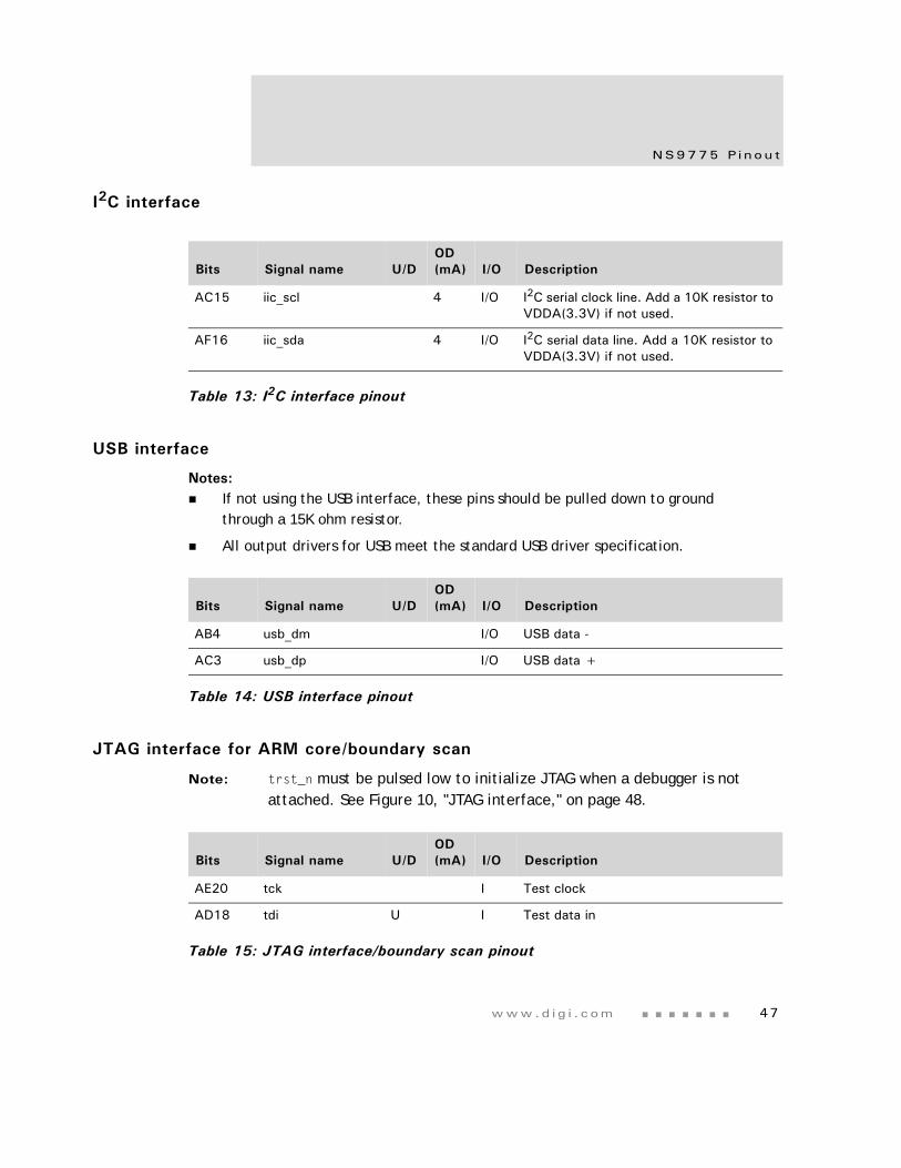
www.d i g i . com 47
NS9775 P i nou t
I2C interface
USB interface
Notes:If not using the USB interface, these pins should be pulled down to ground through a 15K ohm resistor.
All output drivers for USB meet the standard USB driver specification.
JTAG interface for ARM core/boundary scan
Note: trst_n must be pulsed low to initialize JTAG when a debugger is not attached. See Figure 10, "JTAG interface," on page 48.
Bits Signal name U/DOD (mA) I/O Description
AC15 iic_scl 4 I/O I2C serial clock line. Add a 10K resistor to VDDA(3.3V) if not used.
AF16 iic_sda 4 I/O I2C serial data line. Add a 10K resistor to VDDA(3.3V) if not used.
Table 13: I2C interface pinout
Bits Signal name U/DOD (mA) I/O Description
AB4 usb_dm I/O USB data -
AC3 usb_dp I/O USB data +
Table 14: USB interface pinout
Bits Signal name U/DOD (mA) I/O Description
AE20 tck I Test clock
AD18 tdi U I Test data in
Table 15: JTAG interface/boundary scan pinout
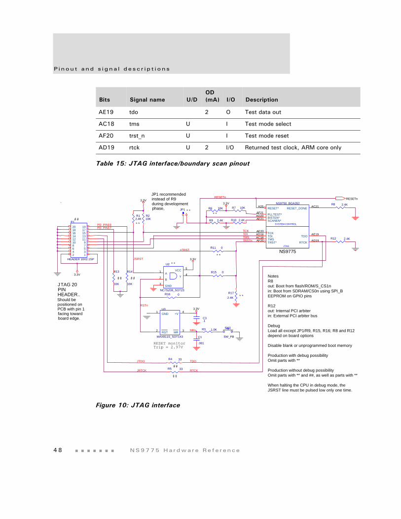
P i nou t a nd s i g na l d e s c r i p t i o n s
4 8 NS9775 Ha r dwa r e Re f e r ence
Figure 10: JTAG interface
AE19 tdo 2 O Test data out
AC18 tms U I Test mode select
AF20 trst_n U I Test mode reset
AD19 rtck U 2 I/O Returned test clock, ARM core only
Bits Signal name U/DOD (mA) I/O Description
Table 15: JTAG interface/boundary scan pinout
TRSTn
R15 0
****
R4 33
R13
10K
PD_PIN19
TCK
**3.3V
3.3V
RTCK
##
TDI
U2
NC7SZ08_SOT23
1
2
3
5
4A
B
GND
VCC
Y
RSTn
JSRST
R9 2.4K
##
R7 10K
RESET monitorTrip = 2.97V
R14
10K
JP1
R10 2.4K
R3 1.0K
##JTDO
C3.1
R210K
R16 0
R12 2.4K
JTAG 20PINHEADER..
##
R5 33
TMS
3.3V
PD_PIN17
P1
HEADER 10X2.1SP12345678910
11121314151617181920
R172.4K
SW1
SW_PB
SYSTEM CONTROL
JTAG
NS9750_BGA352H25 AC21
AE20AD18AC18
AE19
AF20 AD19
AF21AD20AE21
RESET* RESET_DONE
TCKTDITMS
TDO
TRST* RTCK
PLLTEST*BISTEN*SCANEN*
R6 10K
Should bepositioned onPCB with pin 1facing towardboard edge.
R8 2.4K
3.3V
RESETn RESETn
JRTCK
U3
MAX811S_SOT143
1
2
4
3
GND
RST
+V
MR
**
R11 0
##
MRn
**
nTRST
TDO
**
C1
.001
R12.4K
JP1 recommendedinstead of R9during development 3.3V
phase,
NS9775
NotesR8out: Boot from flash/ROM/S_CS1nin: Boot from SDRAM/CS0n using SPI_BEEPROM on GPIO pins
R12out: Internal PCI arbiterin: External PCI arbiter bus
DebugLoad all except JP1/R9, R15, R16; R8 and R12depend on board options
Disable blank or unprogrammed boot memory
Production with debug possibilityOmit parts with **
Production without debug possibilityOmit parts with ** and ##, as well as parts with **
When halting the CPU in debug mode, theJSRST line must be pulsed low only one time.
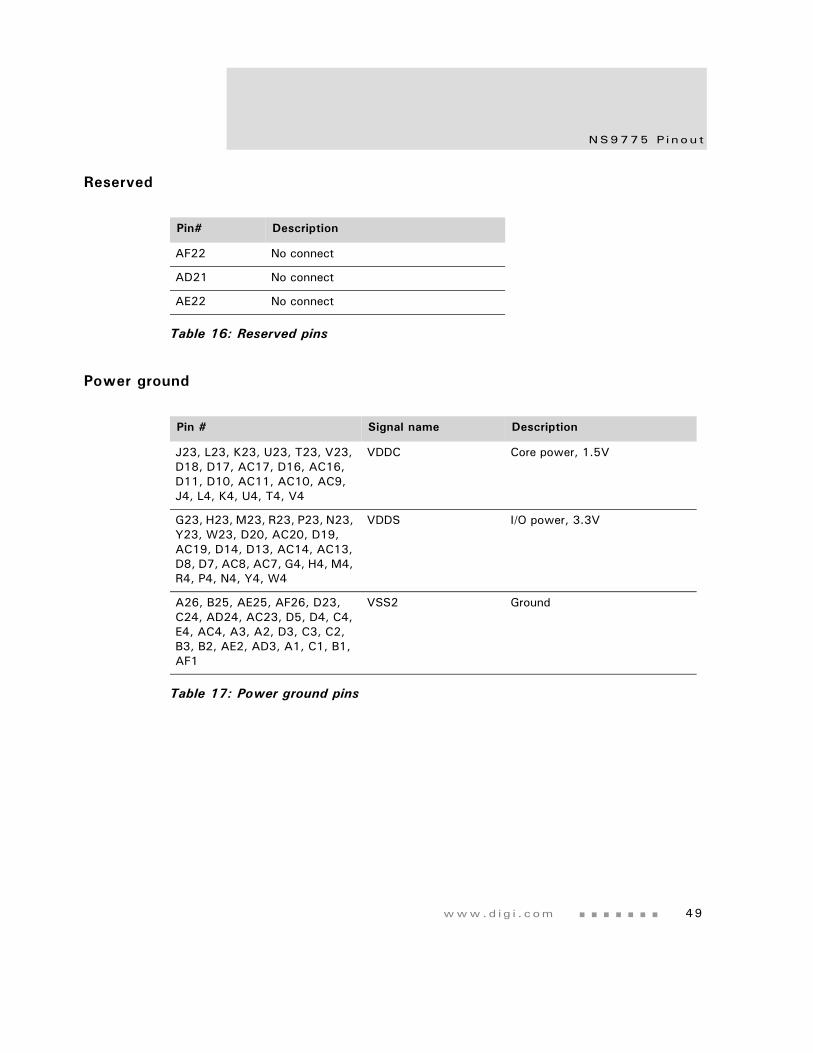
www.d i g i . com 49
NS9775 P i nou t
Reserved
Power ground
Pin# Description
AF22 No connect
AD21 No connect
AE22 No connect
Table 16: Reserved pins
Pin # Signal name Description
J23, L23, K23, U23, T23, V23, D18, D17, AC17, D16, AC16, D11, D10, AC11, AC10, AC9, J4, L4, K4, U4, T4, V4
VDDC Core power, 1.5V
G23, H23, M23, R23, P23, N23, Y23, W23, D20, AC20, D19, AC19, D14, D13, AC14, AC13, D8, D7, AC8, AC7, G4, H4, M4, R4, P4, N4, Y4, W4
VDDS I/O power, 3.3V
A26, B25, AE25, AF26, D23, C24, AD24, AC23, D5, D4, C4, E4, AC4, A3, A2, D3, C3, C2, B3, B2, AE2, AD3, A1, C1, B1, AF1
VSS2 Ground
Table 17: Power ground pins

51
Working with the CPUC H A P T E R 3
The NS9775 core is based on the ARM926EJ-S processor. The ARM926EJ-S processor belongs to the ARM9 family of general-purpose microprocessors. The ARM926EJ-S processor is targeted at multi-tasking applications in which full memory management, high performance, low die size, and low power are important.
Abou t t h e p r o c es so r
5 2 NS9775 Ha r dwa r e Re f e r ence
About the processor
The ARM926EJ-S processor supports the 32-bit ARM and 16-bit Thumb instructions sets, allowing you to trade off between high performance and high code density. The processor includes features for efficient execution of Java byte codes, providing Java performance similar to JIT but without the associated overhead.
The ARM926EJ-S supports the ARM debug architecture, and includes logic to assist in both hardware and software debug. The processor has a Harvard-cached architecture and provides a complete high-performance processor subsystem, including:
ARM926EJ-S integer core
Memory Management Unit (MMU) (see "Memory Management Unit (MMU)," beginning on page 82, for information)
Separate instruction and data AMBA AHB bus interfaces
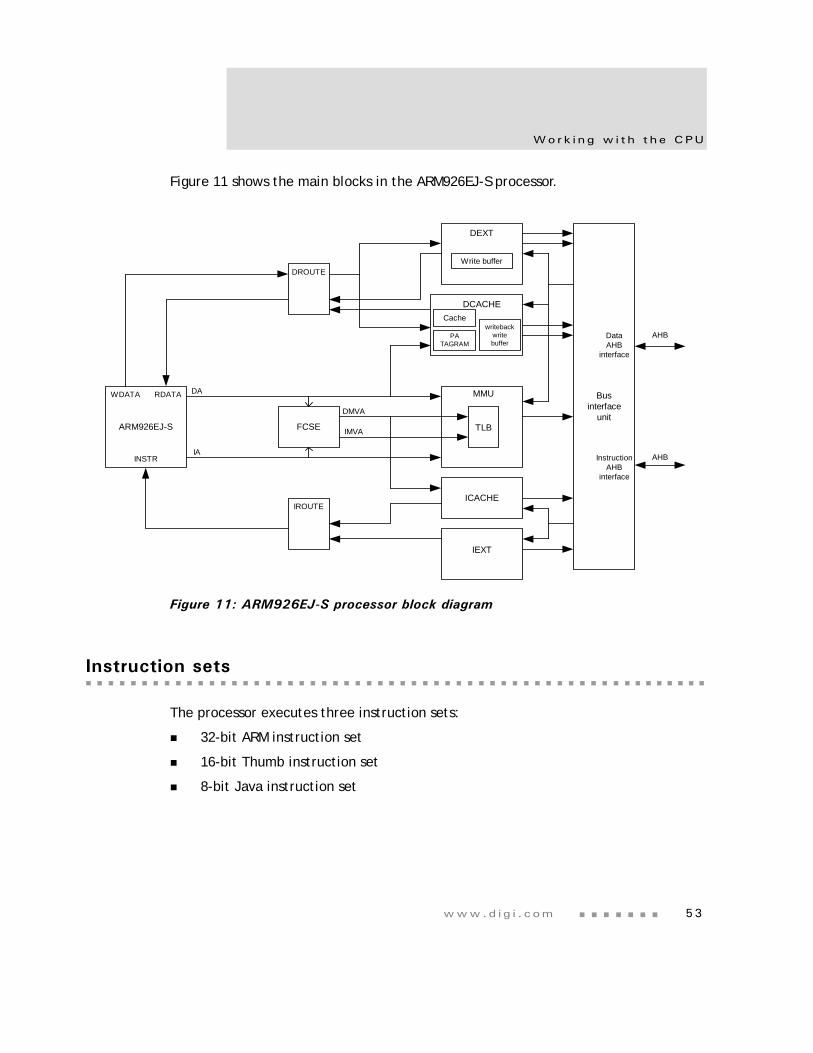
www.d i g i . com 53
Wo rk i ng w i t h t h e CPU
Figure 11 shows the main blocks in the ARM926EJ-S processor.
Figure 11: ARM926EJ-S processor block diagram
Instruction sets
The processor executes three instruction sets:
32-bit ARM instruction set
16-bit Thumb instruction set
8-bit Java instruction set
DEXT
Write buffer
DCACHECache
PATAGRAM
writebackwritebuffer
MMU
TLBARM926EJ-S
IROUTE
DROUTE
FCSE
WDATA RDATA
INSTR
ICACHE
IEXT
Businterface
unit
DataAHB
interface
InstructionAHB
interface
AHB
AHB
DA
IA
DMVA
IMVA
I n s t r u c t i o n s e t s
5 4 NS9775 Ha r dwa r e Re f e r ence
ARM instruction set
The ARM instruction set allows a program to achieve maximum performance with the minimum number of instructions. The majority of instructions are executed in a single cycle.
Thumb instruction set
The Thumb instruction set is simpler than the ARM instruction set, and offers increased code density for code that does not require maximum performance. Code can switch between ARM and Thumb instruction sets on any procedure call.
Java instruction set
In Java state, the processor core executes a majority of Java bytecodes naturally. Bytecodes are decoded in two states, compared to a single decode stage when in ARM/Thumb mode. See "Jazelle (Java)" on page 81 for more information about Java.
www.d i g i . com 55
Wo rk i ng w i t h t h e CPU
System control processor (CP15) registers
The system control processor (CP15) registers configure and control most of the options in the ARM926EJ-S processor. Access the CP15 registers using only the MRC and MCR instructions in a privileged mode; the instructions are provided in the explanation of each applicable register. Using other instructions, or MRC and MCR in unprivileged mode, results in an UNDEFINED instruction exception.
ARM926EJ-S system addresses
The ARM926EJ-S has three distinct types of addresses:
In the ARM926EJ-S domain: Virtual address (VA)
In the Cache and MMU domain: Modified virtual address (MVA)
In the AMBA domain: Physical address (PA)
Example
This is an example of the address manipulation that occurs when the ARM926EJ-S core requests an instruction:
1 The ARM926EJ-S core issues the virtual address of the instruction.
2 The virtual address is translated using the FCSE PID (fast context switch extension process ID) value to the modified virtual address. The instruction cache (ICache) and memory management unit (MMU) find the modified virtual address (see "R13: Process ID register" on page 79).
3 If the protection check carried out by the MMU on the modified virtual address does not abort and the modified virtual address tag is in the ICache, the instruction data is returned to the ARM926EJ-S core.
If the protection check carried out by the MMU on the modified virtual address does not abort but the cache misses (the MVA tag is not in the cache), the MMU translates the modified virtual address to produce the physical address. This address is given to the AMBA bus interface to perform an external access.
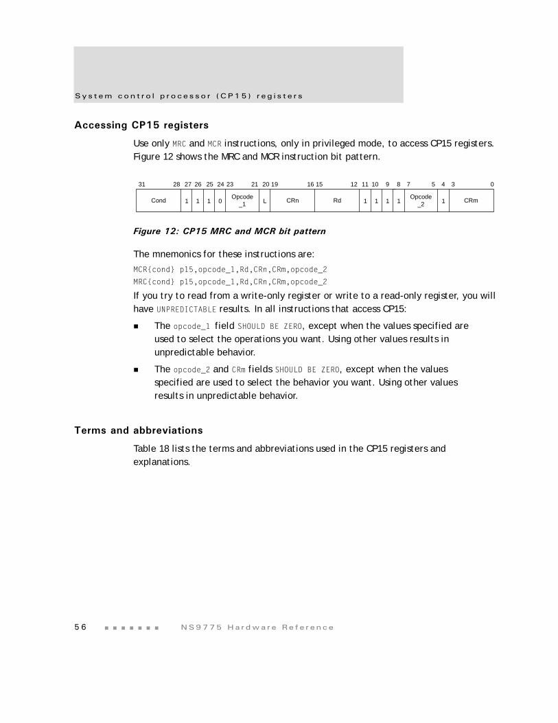
Sys t em con t r o l p r o ce s so r (CP15 ) r eg i s t e r s
5 6 NS9775 Ha r dwa r e Re f e r ence
Accessing CP15 registers
Use only MRC and MCR instructions, only in privileged mode, to access CP15 registers. Figure 12 shows the MRC and MCR instruction bit pattern.
Figure 12: CP15 MRC and MCR bit pattern
The mnemonics for these instructions are:
MCR{cond} p15,opcode_1,Rd,CRn,CRm,opcode_2
MRC{cond} p15,opcode_1,Rd,CRn,CRm,opcode_2
If you try to read from a write-only register or write to a read-only register, you will have UNPREDICTABLE results. In all instructions that access CP15:
The opcode_1 field SHOULD BE ZERO, except when the values specified are used to select the operations you want. Using other values results in unpredictable behavior.
The opcode_2 and CRm fields SHOULD BE ZERO, except when the values specified are used to select the behavior you want. Using other values results in unpredictable behavior.
Terms and abbreviations
Table 18 lists the terms and abbreviations used in the CP15 registers and explanations.
Cond 1 1 1 0 1 1 1 1 1LOpcode
_1Opcode
_2CRn CRmRd
31 28 27 26 25 24 23 21 20 19 16 15 12 11 10 9 8 7 5 4 3 0
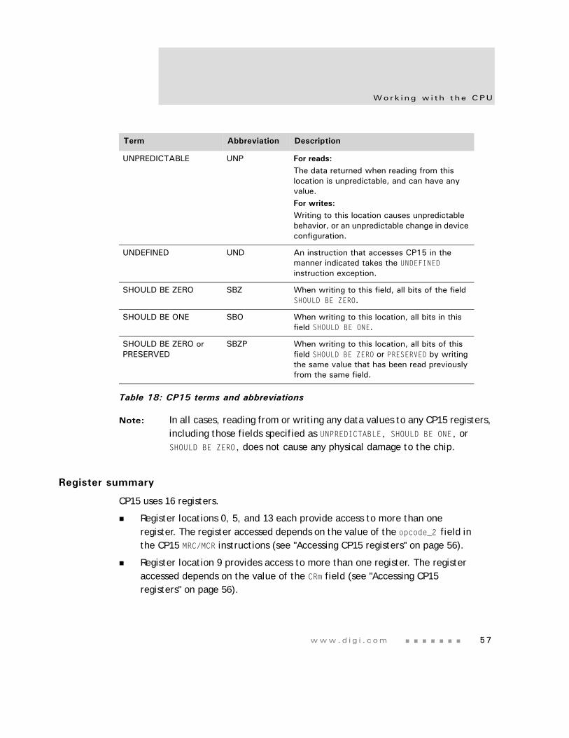
www.d i g i . com 57
Wo rk i ng w i t h t h e CPU
Note: In all cases, reading from or writing any data values to any CP15 registers, including those fields specified as UNPREDICTABLE, SHOULD BE ONE, or SHOULD BE ZERO, does not cause any physical damage to the chip.
Register summary
CP15 uses 16 registers.
Register locations 0, 5, and 13 each provide access to more than one register. The register accessed depends on the value of the opcode_2 field in the CP15 MRC/MCR instructions (see "Accessing CP15 registers" on page 56).
Register location 9 provides access to more than one register. The register accessed depends on the value of the CRm field (see "Accessing CP15 registers" on page 56).
Term Abbreviation Description
UNPREDICTABLE UNP For reads:The data returned when reading from this location is unpredictable, and can have any value.For writes:Writing to this location causes unpredictable behavior, or an unpredictable change in device configuration.
UNDEFINED UND An instruction that accesses CP15 in the manner indicated takes the UNDEFINED instruction exception.
SHOULD BE ZERO SBZ When writing to this field, all bits of the field SHOULD BE ZERO.
SHOULD BE ONE SBO When writing to this location, all bits in this field SHOULD BE ONE.
SHOULD BE ZERO or PRESERVED
SBZP When writing to this location, all bits of this field SHOULD BE ZERO or PRESERVED by writing the same value that has been read previously from the same field.
Table 18: CP15 terms and abbreviations
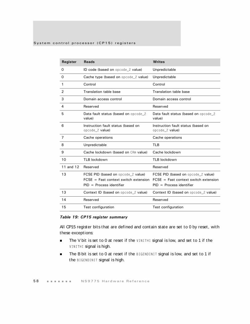
Sys t em con t r o l p r o ce s so r (CP15 ) r eg i s t e r s
5 8 NS9775 Ha r dwa r e Re f e r ence
All CP15 register bits that are defined and contain state are set to 0 by reset, with these exceptions:
The V bit is set to 0 at reset if the VINITHI signal is low, and set to 1 if the VINITHI signal is high.
The B bit is set to 0 at reset if the BIGENDINIT signal is low, and set to 1 if the BIGENDINIT signal is high.
Register Reads Writes
0 ID code (based on opcode_2 value) Unpredictable
0 Cache type (based on opcode_2 value) Unpredictable
1 Control Control
2 Translation table base Translation table base
3 Domain access control Domain access control
4 Reserved Reserved
5 Data fault status (based on opcode_2 value)
Data fault status (based on opcode_2 value)
6 Instruction fault status (based on opcode_2 value)
Instruction fault status (based on opcode_2 value)
7 Cache operations Cache operations
8 Unpredictable TLB
9 Cache lockdown (based on CRm value) Cache lockdown
10 TLB lockdown TLB lockdown
11 and 12 Reserved Reserved
13 FCSE PID (based on opcode_2 value)FCSE = Fast context switch extensionPID = Process identifier
FCSE PID (based on opcode_2 value)FCSE = Fast context switch extensionPID = Process identifier
13 Context ID (based on opcode_2 value) Context ID (based on opcode_2 value)
14 Reserved Reserved
15 Test configuration Test configuration
Table 19: CP15 register summary
www.d i g i . com 59
Wo rk i ng w i t h t h e CPU
R0: ID code and cache type status registers
Register R0 access the ID register, and cache type register. Reading from R0 returns the device ID, and the cache type, depending on the opcode_2 value:
The CRm field SHOULD BE ZERO when reading from these registers. Table 20 shows the instructions you can use to read register R0.
Writing to register R0 is UNPREDICTABLE.
R0: ID code
R0: ID code is a read-only register that returns the 32-bit device ID code. You can access the ID code register by reading CP15 register R0 with the opcode_2 field set to any value other than 1 or 2. Note this example:
MRC p15, 0, Rd, c0, c0, {0, 3-7}; returns ID
Table 21 shows the contents of the ID code register.
opcode_2=0 ID value
opcode_2=1 instruction and data cache type
Function Instruction
Read ID code MRC p15,0,Rd,c0,c0,{0, 3-7}
Read cache type MRC p15,0,Rd,c0,c0,1
Table 20: Reading from register R0
Bits Function Value
[31:24] ASCII code of implementer trademark 0x41
[23:20] Specification revision 0x0
[19:16] Architecture (ARMv5TEJ) 0x6
[15:4] Part number 0x926
[3:0] Layout revision 0x0
Table 21: R0: ID code
Sys t em con t r o l p r o ce s so r (CP15 ) r eg i s t e r s
6 0 NS9775 Ha r dwa r e Re f e r ence
R0: Cache type register
R0: Cache type is a read-only register that contains information about the size and architecture of the instruction cache (ICache) and data cache (DCache) enabling operating systems to establish how to perform operations such as cache cleaning and lockdown. See "Cache features" on page 109 for more information about cache.
You can access the cache type register by reading CP15 register R0 with the opcode_2 field set to 1. Note this example:
MRC p15, 0, Rd, c0, c0, 1; returns cache details
Figure 13 shows the format of the cache type register. Table 22 describes the fields in the register.
Figure 13: Cache type register format
Field Description
Ctype Determines the cache type, and specifies whether the cache supports lockdown and how it is cleaned. Ctype encoding is shown below; all unused values are reserved.Value: 0b1110Method: WritebackCache cleaning: Register 7 operations (see "R7: Cache Operations register" on page 68)Cache lockdown: Format C (see "R9: Cache Lockdown register" on page 74)
S bit Specifies whether the cache is a unified cache (S=0) or separate ICache and DCache (S=1). Will always report separate ICache and DCache for NS9775.
Dsize Specifies the size, line length, and associativity of the DCache.
Isize Species the size, length and associativity of the ICache.
Table 22: Cache type register field definition
Ctype0 S Dsize
31 28 25 24 23 12
0 0 Isize
www.d i g i . com 61
Wo rk i ng w i t h t h e CPU
Dsize and Isize fieldsThe Dsize and Isize fields in the cache type register have the same format, as shown:
The field contains these bits:
Field Description
Size Determines the cache size in conjunction with the M bit.
The M bit is 0 for DCache and ICache.
The size field is bits [21:18] for the DCache and bits [9:6] for the ICache.
The minimum size of each cache is 4 KB; the maximum size is 128 KB.
Cache size encoding with M=0:Size field Cache size0b0011 4 KB0b0100 8 KB
Note: The NS9775 always reports 4KB for DCache and 8KB for ICache.
Assoc Determines the cache associativity in conjunction with the M bit.
The M bit is 0 for both DCache and ICache.
The assoc field is bits [17:15 for the DCache and bits [5:3] for the ICache.
Cache associativity with encoding:Assoc field Associativity0b010 4-wayOther values Reserved
M bit Multiplier bit. Determines the cache size and cache associativity values in conjunction with the size and assoc fields.
Note: This field must be set to 0 for the ARM926EJ-S processor.
Len Determines the line length of the cache.
The len field is bits [13:12] for the DCache and bits [1:0] for the ICache.
Line length encoding:Len field Cache line length10 8 words (32 bytes)Other values Reserved
11 10 9 6 5 3 2 1 0
0 0 Size MAssoc Len
Sys t em con t r o l p r o ce s so r (CP15 ) r eg i s t e r s
6 2 NS9775 Ha r dwa r e Re f e r ence
R1: Control register
Register R1 is the control register for the ARM926EJ-S processor. This register specifies the configuration used to enable and disable the caches and MMU (memory management unit). It is recommended that you access this register using a read-modify-write sequence.
For both reading and writing, the CRm and opcode_2 fields SHOULD BE ZERO. Use these instructions to read and write this register:
MRC p15, 0, Rd, c1, c0, 0 ; read control registerMCR p15, Rd, c1, c0, 0 ; write control register
All defined control bits are set to zero on reset except the V bit and B bit.
The V bit is set to zero at reset if the VINITHI signal is low.
The B bit is set to zero at reset if the BIGENDINIT signal is low, and set to one if the BIGENDINIT signal is high.
Figure 14 shows the Control register format. Table 23 describes the Control register bit functionality.
Figure 14: Control register format
Bits Name Function
[31:19] N/A Reserved:
When read, returns an UNPREDICTABLE value.
When written, SHOULD BE ZERO, or a value read from bits [31:19] on the same processor.
Use a read-modify-write sequence when modifying this register to provide the greatest future compatibility.
[18] N/A Reserved, SBO. Read = 1, write =1.
[17] N/A Reserved, SBZ. read = 0, write = 0.
[16] N/A Reserved, SBO. Read = 1, write = 1.
Table 23: R1: Control register bit definition
131 19 16 15 12 11 10 9 8 7 3 0218 17 14 13 6SBZ
SBZSBO
SBO
L4
RR V I SBZ R S B SBO C A M
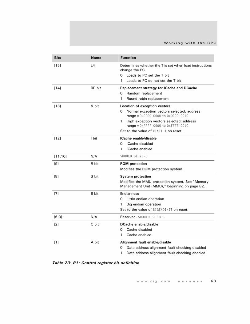
www.d i g i . com 63
Wo rk i ng w i t h t h e CPU
[15] L4 Determines whether the T is set when load instructions change the PC.0 Loads to PC set the T bit1 Loads to PC do not set the T bit
[14] RR bit Replacement strategy for ICache and DCache0 Random replacement1 Round-robin replacement
[13] V bit Location of exception vectors0 Normal exception vectors selected; address
range=0x0000 0000 to 0x0000 001C1 High exception vectors selected; address
range=0xFFFF 0000 to 0xFFFF 001CSet to the value of VINITHI on reset.
[12] I bit ICache enable/disable0 ICache disabled1 ICache enabled
[11:10] N/A SHOULD BE ZERO
[9] R bit ROM protectionModifies the ROM protection system.
[8] S bit System protectionModifies the MMU protection system. See "Memory Management Unit (MMU)," beginning on page 82.
[7] B bit Endianness0 Little endian operation1 Big endian operationSet to the value of BIGENDINIT on reset.
[6:3] N/A Reserved. SHOULD BE ONE.
[2] C bit DCache enable/disable0 Cache disabled1 Cache enabled
[1] A bit Alignment fault enable/disable0 Data address alignment fault checking disabled1 Data address alignment fault checking enabled
Bits Name Function
Table 23: R1: Control register bit definition
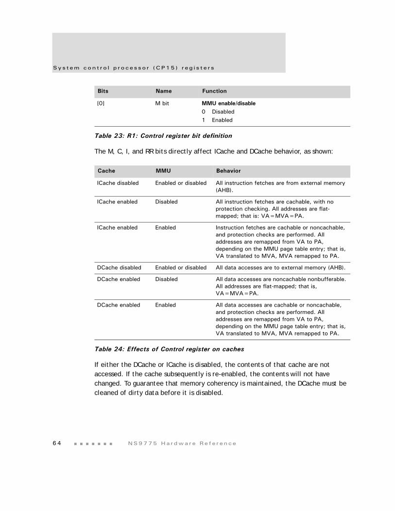
Sys t em con t r o l p r o ce s so r (CP15 ) r eg i s t e r s
6 4 NS9775 Ha r dwa r e Re f e r ence
The M, C, I, and RR bits directly affect ICache and DCache behavior, as shown:
If either the DCache or ICache is disabled, the contents of that cache are not accessed. If the cache subsequently is re-enabled, the contents will not have changed. To guarantee that memory coherency is maintained, the DCache must be cleaned of dirty data before it is disabled.
[0] M bit MMU enable/disable0 Disabled1 Enabled
Cache MMU Behavior
ICache disabled Enabled or disabled All instruction fetches are from external memory (AHB).
ICache enabled Disabled All instruction fetches are cachable, with no protection checking. All addresses are flat-mapped; that is: VA=MVA=PA.
ICache enabled Enabled Instruction fetches are cachable or noncachable, and protection checks are performed. All addresses are remapped from VA to PA, depending on the MMU page table entry; that is, VA translated to MVA, MVA remapped to PA.
DCache disabled Enabled or disabled All data accesses are to external memory (AHB).
DCache enabled Disabled All data accesses are noncachable nonbufferable. All addresses are flat-mapped; that is, VA=MVA=PA.
DCache enabled Enabled All data accesses are cachable or noncachable, and protection checks are performed. All addresses are remapped from VA to PA, depending on the MMU page table entry; that is, VA translated to MVA, MVA remapped to PA.
Table 24: Effects of Control register on caches
Bits Name Function
Table 23: R1: Control register bit definition
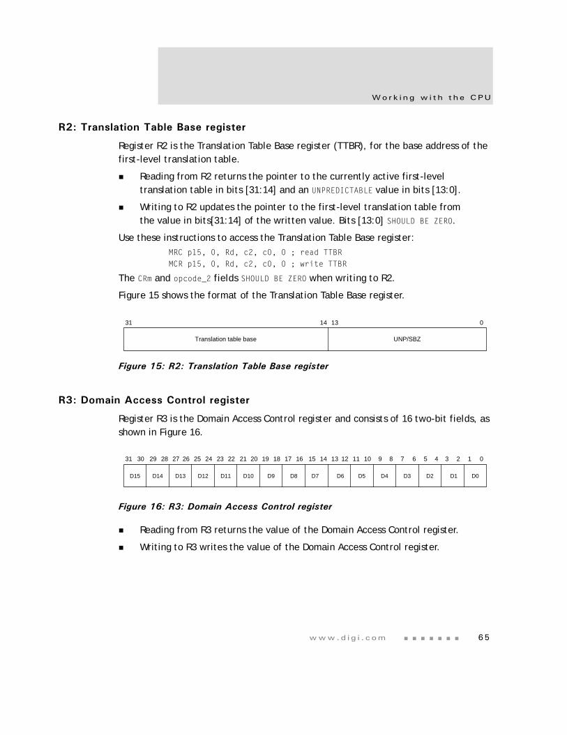
www.d i g i . com 65
Wo rk i ng w i t h t h e CPU
R2: Translation Table Base register
Register R2 is the Translation Table Base register (TTBR), for the base address of the first-level translation table.
Reading from R2 returns the pointer to the currently active first-level translation table in bits [31:14] and an UNPREDICTABLE value in bits [13:0].
Writing to R2 updates the pointer to the first-level translation table from the value in bits[31:14] of the written value. Bits [13:0] SHOULD BE ZERO.
Use these instructions to access the Translation Table Base register:MRC p15, 0, Rd, c2, c0, 0 ; read TTBRMCR p15, 0, Rd, c2, c0, 0 ; write TTBR
The CRm and opcode_2 fields SHOULD BE ZERO when writing to R2.
Figure 15 shows the format of the Translation Table Base register.
Figure 15: R2: Translation Table Base register
R3: Domain Access Control register
Register R3 is the Domain Access Control register and consists of 16 two-bit fields, as shown in Figure 16.
Figure 16: R3: Domain Access Control register
Reading from R3 returns the value of the Domain Access Control register.
Writing to R3 writes the value of the Domain Access Control register.
31 014 13
Translation table base UNP/SBZ
31 014 13 12 11 10 9 8 7 6 5 4 3 2 115161718192021222324252627282930
D0D1D2D3D4D5D6D7D8D9D10D11D12D13D14D15
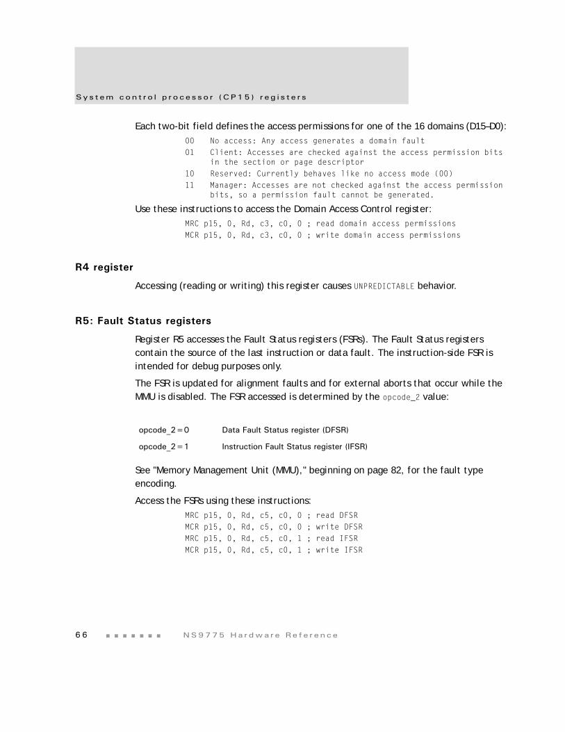
Sys t em con t r o l p r o ce s so r (CP15 ) r eg i s t e r s
6 6 NS9775 Ha r dwa r e Re f e r ence
Each two-bit field defines the access permissions for one of the 16 domains (D15–D0):00 No access: Any access generates a domain fault
01 Client: Accesses are checked against the access permission bits in the section or page descriptor
10 Reserved: Currently behaves like no access mode (00)11 Manager: Accesses are not checked against the access permission
bits, so a permission fault cannot be generated.
Use these instructions to access the Domain Access Control register:MRC p15, 0, Rd, c3, c0, 0 ; read domain access permissionsMCR p15, 0, Rd, c3, c0, 0 ; write domain access permissions
R4 register
Accessing (reading or writing) this register causes UNPREDICTABLE behavior.
R5: Fault Status registers
Register R5 accesses the Fault Status registers (FSRs). The Fault Status registers contain the source of the last instruction or data fault. The instruction-side FSR is intended for debug purposes only.
The FSR is updated for alignment faults and for external aborts that occur while the MMU is disabled. The FSR accessed is determined by the opcode_2 value:
See "Memory Management Unit (MMU)," beginning on page 82, for the fault type encoding.
Access the FSRs using these instructions:MRC p15, 0, Rd, c5, c0, 0 ; read DFSRMCR p15, 0, Rd, c5, c0, 0 ; write DFSRMRC p15, 0, Rd, c5, c0, 1 ; read IFSR
MCR p15, 0, Rd, c5, c0, 1 ; write IFSR
opcode_2=0 Data Fault Status register (DFSR)
opcode_2=1 Instruction Fault Status register (IFSR)
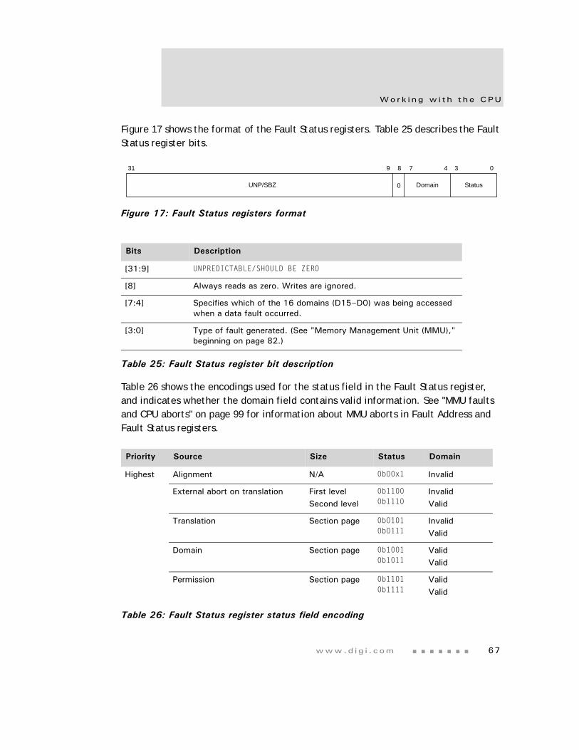
www.d i g i . com 67
Wo rk i ng w i t h t h e CPU
Figure 17 shows the format of the Fault Status registers. Table 25 describes the Fault Status register bits.
Figure 17: Fault Status registers format
Table 26 shows the encodings used for the status field in the Fault Status register, and indicates whether the domain field contains valid information. See "MMU faults and CPU aborts" on page 99 for information about MMU aborts in Fault Address and Fault Status registers.
Bits Description
[31:9] UNPREDICTABLE/SHOULD BE ZERO
[8] Always reads as zero. Writes are ignored.
[7:4] Specifies which of the 16 domains (D15–D0) was being accessed when a data fault occurred.
[3:0] Type of fault generated. (See "Memory Management Unit (MMU)," beginning on page 82.)
Table 25: Fault Status register bit description
Priority Source Size Status Domain
Highest Alignment N/A 0b00x1 Invalid
External abort on translation First levelSecond level
0b11000b1110
InvalidValid
Translation Section page 0b01010b0111
InvalidValid
Domain Section page 0b10010b1011
ValidValid
Permission Section page 0b11010b1111
ValidValid
Table 26: Fault Status register status field encoding
31 09 8 7 4 3
0UNP/SBZ Domain Status
Sys t em con t r o l p r o ce s so r (CP15 ) r eg i s t e r s
6 8 NS9775 Ha r dwa r e Re f e r ence
R6: Fault Address register
Register R6 accesses the Fault Address register (FAR). The Fault Address register contains the modified virtual address of the access attempted when a data abort occurred. This register is updated only for data aborts, not for prefetch aborts; it is updated also for alignment faults and external aborts that occur while the MMU is disabled.
Use these instructions to access the Fault Address register:MRC p15, 0, Rd, c6, c0, 0 ; read FARMCR p15, 0, Rd, c6, c0, 0 ; write FAR
Writing R6 sets the Fault Address register to the value of the data written. This is useful for debugging, to restore the value of a Fault Address register to a previous state.
The CRm and opcode_2 fields SHOULD BE ZERO when reading or writing R6.
R7: Cache Operations register
Register R7 controls the caches and write buffer. The function of each cache operation is selected by the opcode_2 and CRm fields in the MCR instruction that writes to CP15 R7. Writing other opcode_2 or CRm values is UNPREDICTABLE.
Reading from R7 is UNPREDICTABLE, with the exception of the two test and clean operations (see Table 28, “R7: Cache operations,” on page 70 and "Test and clean operations" on page 72).
Use this instruction to write to the Cache Operations register:MCR p15, opcode_1, Rd, CRn, CRm, opcode_2
Table 27 describes the cache functions provided by register R7. Table 28 lists the cache operation functions and associated data and instruction formats for R7.
Lowest External abort Section page 0b10000b1010
ValidValid
Priority Source Size Status Domain
Table 26: Fault Status register status field encoding
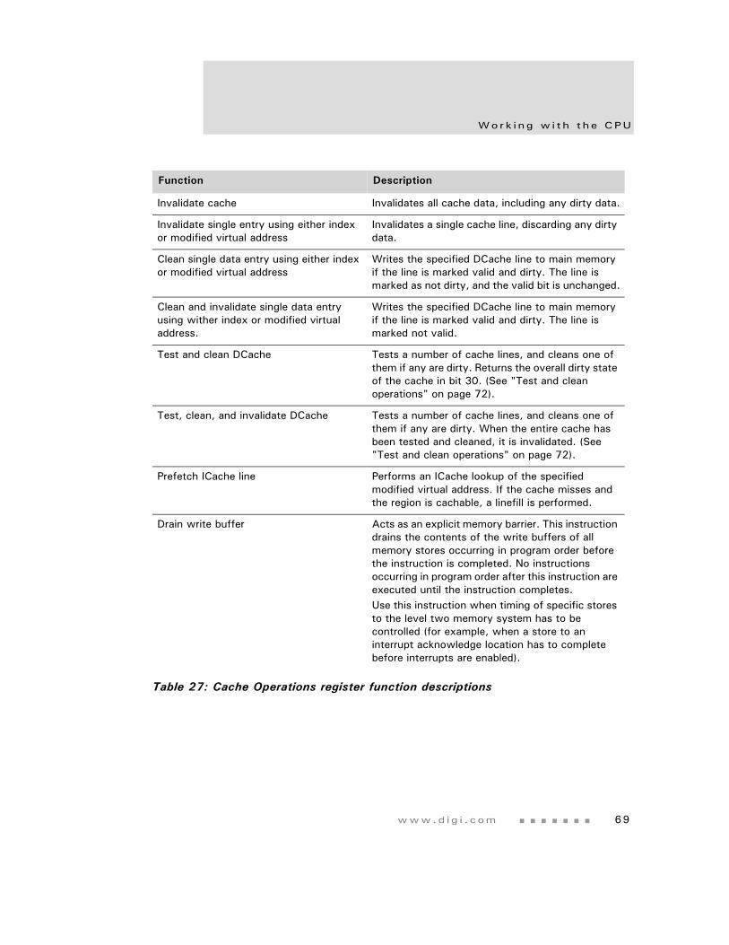
www.d i g i . com 69
Wo rk i ng w i t h t h e CPU
Function Description
Invalidate cache Invalidates all cache data, including any dirty data.
Invalidate single entry using either index or modified virtual address
Invalidates a single cache line, discarding any dirty data.
Clean single data entry using either index or modified virtual address
Writes the specified DCache line to main memory if the line is marked valid and dirty. The line is marked as not dirty, and the valid bit is unchanged.
Clean and invalidate single data entry using wither index or modified virtual address.
Writes the specified DCache line to main memory if the line is marked valid and dirty. The line is marked not valid.
Test and clean DCache Tests a number of cache lines, and cleans one of them if any are dirty. Returns the overall dirty state of the cache in bit 30. (See "Test and clean operations" on page 72).
Test, clean, and invalidate DCache Tests a number of cache lines, and cleans one of them if any are dirty. When the entire cache has been tested and cleaned, it is invalidated. (See "Test and clean operations" on page 72).
Prefetch ICache line Performs an ICache lookup of the specified modified virtual address. If the cache misses and the region is cachable, a linefill is performed.
Drain write buffer Acts as an explicit memory barrier. This instruction drains the contents of the write buffers of all memory stores occurring in program order before the instruction is completed. No instructions occurring in program order after this instruction are executed until the instruction completes. Use this instruction when timing of specific stores to the level two memory system has to be controlled (for example, when a store to an interrupt acknowledge location has to complete before interrupts are enabled).
Table 27: Cache Operations register function descriptions
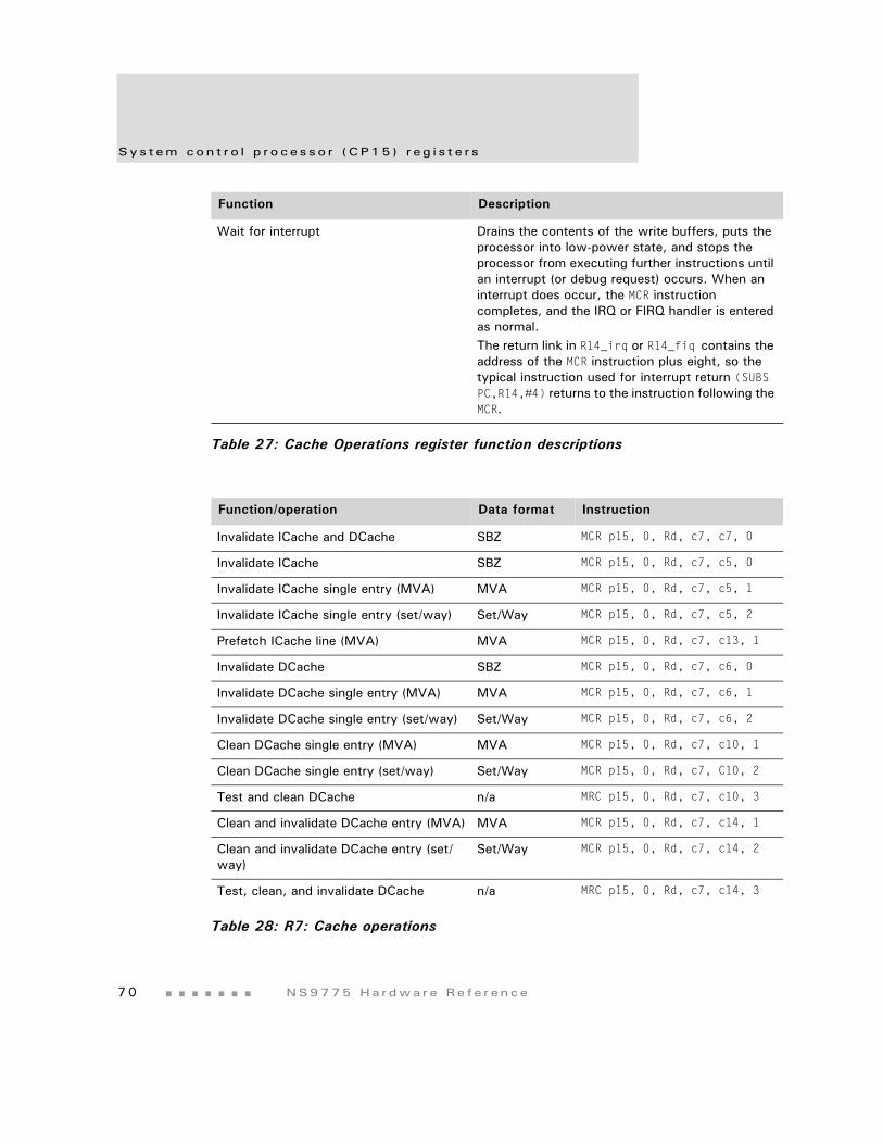
Sys t em con t r o l p r o ce s so r (CP15 ) r eg i s t e r s
7 0 NS9775 Ha r dwa r e Re f e r ence
Wait for interrupt Drains the contents of the write buffers, puts the processor into low-power state, and stops the processor from executing further instructions until an interrupt (or debug request) occurs. When an interrupt does occur, the MCR instruction completes, and the IRQ or FIRQ handler is entered as normal. The return link in R14_irq or R14_fiq contains the address of the MCR instruction plus eight, so the typical instruction used for interrupt return (SUBS PC,R14,#4) returns to the instruction following the MCR.
Function/operation Data format Instruction
Invalidate ICache and DCache SBZ MCR p15, 0, Rd, c7, c7, 0
Invalidate ICache SBZ MCR p15, 0, Rd, c7, c5, 0
Invalidate ICache single entry (MVA) MVA MCR p15, 0, Rd, c7, c5, 1
Invalidate ICache single entry (set/way) Set/Way MCR p15, 0, Rd, c7, c5, 2
Prefetch ICache line (MVA) MVA MCR p15, 0, Rd, c7, c13, 1
Invalidate DCache SBZ MCR p15, 0, Rd, c7, c6, 0
Invalidate DCache single entry (MVA) MVA MCR p15, 0, Rd, c7, c6, 1
Invalidate DCache single entry (set/way) Set/Way MCR p15, 0, Rd, c7, c6, 2
Clean DCache single entry (MVA) MVA MCR p15, 0, Rd, c7, c10, 1
Clean DCache single entry (set/way) Set/Way MCR p15, 0, Rd, c7, C10, 2
Test and clean DCache n/a MRC p15, 0, Rd, c7, c10, 3
Clean and invalidate DCache entry (MVA) MVA MCR p15, 0, Rd, c7, c14, 1
Clean and invalidate DCache entry (set/way)
Set/Way MCR p15, 0, Rd, c7, c14, 2
Test, clean, and invalidate DCache n/a MRC p15, 0, Rd, c7, c14, 3
Table 28: R7: Cache operations
Function Description
Table 27: Cache Operations register function descriptions
www.d i g i . com 71
Wo rk i ng w i t h t h e CPU
Figure 18 shows the modified virtual address format for Rd for the CP15 R7 MCR operations.
The tag, set, and word fields define the MVA.
For all cache operations, the word field SHOULD BE ZERO.
Figure 18: R7: MVA format
Figure 19 shows the Set/Way format for Rd for the CP15 R7 MCR operations.
A and S are the base-two logarithms of the associativity and the number of sets.
The set, way, and word files define the format.
For all of the cache operations, word SHOULD BE ZERO.
For example, a 16 KB cache, 4-way set associative, 8-word line results in the following:
A = log2 associativity = log24 = 2
S = log2 NSETS where
NSETS = cache size in bytes/associativity/line length in bytes:
NSETS = 16384/4/32 = 128
Result: S = log2 128 = 7
Figure 19: R7: Set/Way format
Drain write buffer SBZ MCR p15, 0, Rd, c7, c10, 4
Wait for interrupt SBZ MCR p15, 0, Rd, c7, c0, 4
Function/operation Data format Instruction
Table 28: R7: Cache operations
31 0S+4 4
SBZSet(=index) WordTag
2 15S+5
31 0S+4 4
SBZSet(=index) WordSBZ
2 15S+5
Way
32-A 31-A
Sys t em con t r o l p r o ce s so r (CP15 ) r eg i s t e r s
7 2 NS9775 Ha r dwa r e Re f e r ence
Test and clean operations
Test and clean DCache instructionThe test and clean DCache instruction provides an efficient way to clean the entire DCache, using a simple loop. The test and clean DCache instruction tests a number of lines in the DCache to determine whether any of them are dirty. If any dirty lines are found, one of those lines is cleaned. The test and clean DCache instruction also returns the status of the entire DCache in bit 30.
Note: The test and clean DCache instruction MRC p15, 0, r15, c7, c10, 3 is a special encoding that uses r15 as a destination operand. The PC is not changed by using this instruction, however. This MRC instruction also sets the condition code flags.
If the cache contains any dirty lines, bit 30 is set to 0. If the cache contains no dirty lines, bit 30 is set to 1. Use the following loop to clean the entire cache:
tc_loop: MRC p15, 0, r15, c7, c10, 3 ; test and cleanBNE tc_loop
Test, clean, and invalidate DCache instructionThe test, clean, and invalidate DCache instruction is the same as the test and clean DCache instruction except that when the entire cache has been cleaned, it is invalidated. Use the following loop to test, clean, and invalidate the entire DCache:
tci_loop: MRC p15, 0, r15, c7, c14, 3 ; test clean and invalidateBNE tci_loop
R8:TLB Operations register
Register R8 is a write-only register that controls the translation lookaside buffer (TLB). There is a single TLB used to hold entries for both data and instructions. The TLB is divided into two parts:
Set-associative
Fully-associative
The fully-associative part (also referred to as the lockdown part of the TLB) stores entries to be locked down. Entries held in the lockdown part of the register are preserved during an invalidate-TLB operation. Entries can be removed from the lockdown TLB using an invalidate TLB single entry operation.
www.d i g i . com 73
Wo rk i ng w i t h t h e CPU
There are six TLB operations; the function to be performed is selected by the opcode_2 and CRm fields in the MCR instruction used to write register R8. Writing other opcode_2 or CRm values is UNPREDICTABLE. Reading from this register is UNPREDICTABLE.
Use the instruction shown in Table 29 to perform TLB operations.
The invalidate TLB operations invalidate all the unpreserved entries in the TLB.
The invalidate TLB single entry operations invalidate any TLB entry corresponding to the modified virtual address given in Rd, regardless of its preserved state. See "R10: TLB Lockdown register," beginning on page 77, for an explanation of how to preserve TLB entries.
Figure 20 shows the modified virtual address format used for invalid TLB single entry operations.
Figure 20: R8: TLB Operations, MVA format
Note: If either small or large pages are used, and these pages contain subpage access permissions that are different, you must use four invalidate TLB single entry operations, with the MVA set to each subpage, to invalidate all information related to that page held in a TLB.
Operation Data Instruction
Invalidate set-associative TLB SBZ MCR p15, 0, Rd, c8, c7, 0
Invalidate single entry SBZ MCR p15, 0, Rd, c8, c7. 1
Invalidate set-associative TLB SBZ MCR p15, 0, Rd, c8, c5, 0
Invalidate single entry MVA MCR p15, 0, Rd, c8, c5, 1
Invalidate set-associative TLB SBZ MCR p15, 0, Rd, c8, c6, 0
Invalidate single entry MVA MCR p15, 0, Rd, c8, c6, 1
Table 29: R8: Translation Lookaside Buffer operations
31 09
SBZModified virtual address
10
Sys t em con t r o l p r o ce s so r (CP15 ) r eg i s t e r s
7 4 NS9775 Ha r dwa r e Re f e r ence
R9: Cache Lockdown register
Register R9 access the cache lockdown registers. Access this register using CRm = 0.
The Cache Lockdown register uses a cache-way-based locking scheme (format C) that allows you to control each cache way independently.
These registers allow you to control which cache-ways of the four-way cache are used for the allocation on a linefill. When the registers are defined, subsequent linefills are placed only in the specified target cache way. This gives you some control over the cache pollution cause by particular applications, and provides a traditional lockdown operation for locking critical code into the cache.
A locking bit for each cache way determines whether the normal cache allocation is allowed to access that cache way (see Table 31, “Cache Lockdown register L bits,” on page 75). A maximum of three cache ways of the four-way associative cache can be locked, ensuring that normal cache line replacement is performed.
Note: If no cache ways have the L bit set to 0, cache way 3 is used for all linefills.
The first four bits of this register determine the L bit for the associated cache way. The opcode_2 field of the MRC or MCR instruction determines whether the instruction or data lockdown register is accessed:
Use the instructions shown in Table 30 to access the CacheLockdown register.
opcode_2=0 Selects the DCache Lockdown register, or the Unified Cache Lockdown register if a unified cache is implemented. The ARM926EJ-S processor has separate DCache and ICache.
opcode_2=1 Selects the ICache Lockdown register.
Function Data Instruction
Read DCache Lockdown register L bits MRC p15, 0, Rd, c9, c0, 0
Write DCache Lockdown register L bits MCR p15, 0, Rd, c9, c0, 0
Read ICache Lockdown register L bits MRC p15, 0, Rd, c9, c0, 1
Write ICache Lockdown register L bits MCR p15, 0, Rd, c9, c0, 1
Table 30: Cache Lockdown register instructions
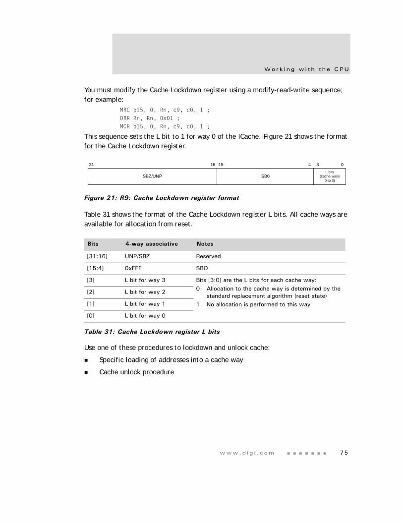
www.d i g i . com 75
Wo rk i ng w i t h t h e CPU
You must modify the Cache Lockdown register using a modify-read-write sequence; for example:
MRC p15, 0, Rn, c9, c0, 1 ;ORR Rn, Rn, 0x01 ;
MCR p15, 0, Rn, c9, c0, 1 ;
This sequence sets the L bit to 1 for way 0 of the ICache. Figure 21 shows the format for the Cache Lockdown register.
Figure 21: R9: Cache Lockdown register format
Table 31 shows the format of the Cache Lockdown register L bits. All cache ways are available for allocation from reset.
Use one of these procedures to lockdown and unlock cache:
Specific loading of addresses into a cache way
Cache unlock procedure
Bits 4-way associative Notes
[31:16] UNP/SBZ Reserved
[15:4] 0xFFF SBO
[3] L bit for way 3 Bits [3:0] are the L bits for each cache way:0 Allocation to the cache way is determined by the
standard replacement algorithm (reset state)1 No allocation is performed to this way
[2] L bit for way 2
[1] L bit for way 1
[0] L bit for way 0
Table 31: Cache Lockdown register L bits
31 03
SBZ/UNP
15 416
SB0L bits
(cache ways0 to 3)
Sys t em con t r o l p r o ce s so r (CP15 ) r eg i s t e r s
7 6 NS9775 Ha r dwa r e Re f e r ence
Specific loading of addresses into a cache-way
The procedure to lock down code and data into way i of cache, with N ways, using format C, makes it impossible to allocate to any cache way other than the target cache way:
1 Ensure that no processor exceptions can occur during the execution of this procedure; for example, disable interrupts. If this is not possible, all code and data used by any exception handlers must be treated as code and data as in Steps 2 and 3.
2 If an ICache way is being locked down, be sure that all the code executed by the lockdown procedure is in an uncachable area of memory or in an already locked cache way.
3 If a DCache way is being locked down, be sure that all data used by the lockdown procedure is in an uncachable area of memory or is in an already locked cache way.
4 Ensure that the data/instructions that are to be locked down are in a cachable area of memory.
5 Be sure that the data/instructions that are to be locked down are not already in the cache. Use the Cache Operations register (R7) clean and/or invalidate functions to ensure this.
6 Write these settings to the Cache Lockdown register (R9), to enable allocation to the target cache way:
CRm = 0
Set L == 0 for bit i
Set L == 1 for all other bits
7 For each of the cache lines to be locked down in cache way i:
– If a DCache is being locked down, use an LDR instruction to load a word from the memory cache line to ensure that the memory cache line is loaded into the cache.
– If an ICache is being locked down, use the Cache Operations register (R7) MCR prefetch ICache line (<CRm>==c13, <opcode2>==1) to fetch the memory cache line into the cache.
8 Write <CRm>==0 to Cache Lockdown register (R9), setting L==1 for bit i and restoring all other bits to the values they had before the lockdown routine was started.
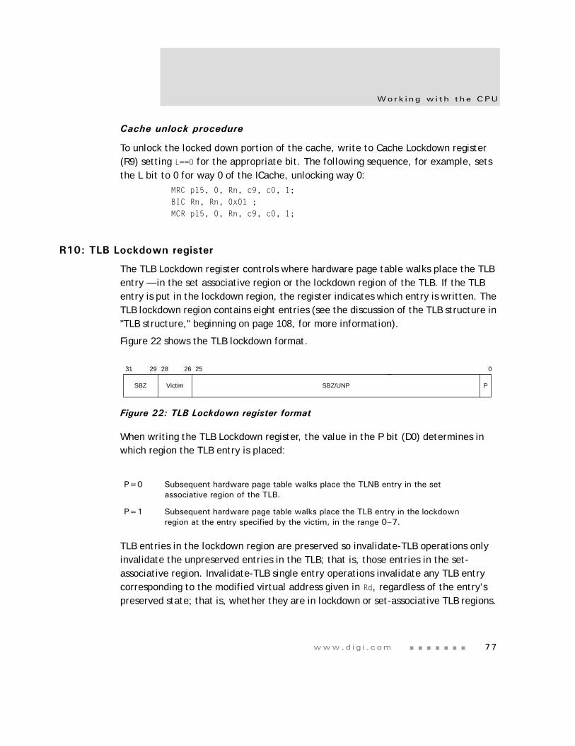
www.d i g i . com 77
Wo rk i ng w i t h t h e CPU
Cache unlock procedure
To unlock the locked down portion of the cache, write to Cache Lockdown register (R9) setting L==0 for the appropriate bit. The following sequence, for example, sets the L bit to 0 for way 0 of the ICache, unlocking way 0:
MRC p15, 0, Rn, c9, c0, 1;
BIC Rn, Rn, 0x01 ;MCR p15, 0, Rn, c9, c0, 1;
R10: TLB Lockdown register
The TLB Lockdown register controls where hardware page table walks place the TLB entry — in the set associative region or the lockdown region of the TLB. If the TLB entry is put in the lockdown region, the register indicates which entry is written. The TLB lockdown region contains eight entries (see the discussion of the TLB structure in "TLB structure," beginning on page 108, for more information).
Figure 22 shows the TLB lockdown format.
Figure 22: TLB Lockdown register format
When writing the TLB Lockdown register, the value in the P bit (D0) determines in which region the TLB entry is placed:
TLB entries in the lockdown region are preserved so invalidate-TLB operations only invalidate the unpreserved entries in the TLB; that is, those entries in the set-associative region. Invalidate-TLB single entry operations invalidate any TLB entry corresponding to the modified virtual address given in Rd, regardless of the entry’s preserved state; that is, whether they are in lockdown or set-associative TLB regions.
P=0 Subsequent hardware page table walks place the TLNB entry in the set associative region of the TLB.
P=1 Subsequent hardware page table walks place the TLB entry in the lockdown region at the entry specified by the victim, in the range 0–7.
Victim SBZ/UNP
31 28 2529 26 0
SBZ P
Sys t em con t r o l p r o ce s so r (CP15 ) r eg i s t e r s
7 8 NS9775 Ha r dwa r e Re f e r ence
See "R8:TLB Operations register" on page 72 for a description of the TLB-invalidate operations.
Use these instructions to program the TLB Lockdown register:
The victim automatically increments after any table walk that results in an entry being written into the lockdown part of the TLB.
Note: It is not possible for a lockdown entry to map entirely either small or large pages, unless all subpage access permissions are the same. Entries can still be written into the lockdown region, but the address range that is mapped covers only the subpage corresponding to the address that was used to perform the page table walk.
Sample code sequenceThis example shows the code sequence that locks down an entry to the current victim.
ADR r1,LockAddr ; set R1 to the value of the address to be locked
down
MCR p15,0,r1,c8,c7,1 ; invalidate TLB single entry to ensure that
LockAddr is not already in the TLB
MRC p15,0,r0,c10,c0,0 ; read the lockdown register
ORR r0,r0,#1 ; set the preserve bit
MCR p15,0,r0,c10,c0,0 ; write to the lockdown register
LDR r1,[r1] ; TLB will miss, and entry will be loaded
MRC p15,0,r0,c10,c0,0 ; read the lockdown register (victim will have
; incremented
BIC r0,r0,#1 ; clear preserve bit
MCR p15,0,r0,c10,c0,0 ; write to the lockdown register
R11 and R12 registers
Accessing (reading or writing) these registers causes UNPREDICTABLE behavior.
Function Instruction
Read data TLB lockdown victim MRC p15, 0, Rd, c10, c0, 0
Write data TLB lockdown victim MCR p15, 0, Rd, c10, c0, 0
www.d i g i . com 79
Wo rk i ng w i t h t h e CPU
R13: Process ID register
The Process ID register accesses the process identifier registers. The register accessed depends on the value on the opcode_2 field:
Use the Process ID register to determine the process that is currently running. The process identifier is set to 0 at reset.
FCSE PID register
Addresses issued by the ARM926EJ-S core, in the range 0 to 32 MB, are translated according to the value contained in the FCSE PID register. Address A becomes A + (FCSE PID x 32 MB); it is this modified address that the MMU and caches see. Addresses above 32 MB are not modified. The FCSE PID is a 7-bit field, which allows 128 x 32 MB processes to be mapped.
If the FCSE PID is 0, there is a flat mapping between the virtual addresses output by the ARM926EJ-S core and the modified virtual addresses used by the caches and MMU. The FCSE PID is set to 0 at system reset.
If the MMU is disabled, there is no FCSE address translation.
FCSE translation is not applied for addresses used for entry-based cache or TLB maintenance operations. For these operations, VA=MVA.
Use these instructions to access the FCSE PID register:
opcode_2=0 Selects the Fast Context Switch Extension (FCSE) Process Identifier (PID) register.
opcode_2=1 Selects the context ID register.
Function Data ARM instruction
Read FCSE PID FCSE PID MRC p15,0,Rd,c13,c0,0
Write FCSE PID FCSE PID MCR p15,0,Rd,c13,c0,0
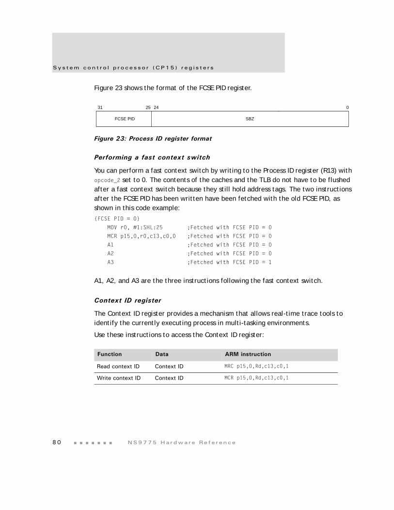
Sys t em con t r o l p r o ce s so r (CP15 ) r eg i s t e r s
8 0 NS9775 Ha r dwa r e Re f e r ence
Figure 23 shows the format of the FCSE PID register.
Figure 23: Process ID register format
Performing a fast context switch
You can perform a fast context switch by writing to the Process ID register (R13) with opcode_2 set to 0. The contents of the caches and the TLB do not have to be flushed after a fast context switch because they still hold address tags. The two instructions after the FCSE PID has been written have been fetched with the old FCSE PID, as shown in this code example:
{FCSE PID = 0}
MOV r0, #1:SHL:25 ;Fetched with FCSE PID = 0
MCR p15,0,r0,c13,c0,0 ;Fetched with FCSE PID = 0
A1 ;Fetched with FCSE PID = 0
A2 ;Fetched with FCSE PID = 0
A3 ;Fetched with FCSE PID = 1
A1, A2, and A3 are the three instructions following the fast context switch.
Context ID register
The Context ID register provides a mechanism that allows real-time trace tools to identify the currently executing process in multi-tasking environments.
Use these instructions to access the Context ID register:
Function Data ARM instruction
Read context ID Context ID MRC p15,0,Rd,c13,c0,1
Write context ID Context ID MCR p15,0,Rd,c13,c0,1
31 25 24 0
SBZFCSE PID
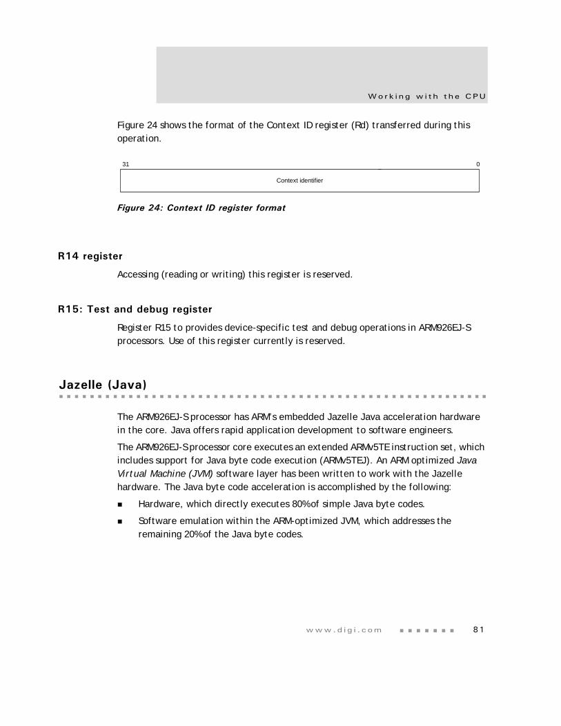
www.d i g i . com 81
Wo rk i ng w i t h t h e CPU
Figure 24 shows the format of the Context ID register (Rd) transferred during this operation.
Figure 24: Context ID register format
R14 register
Accessing (reading or writing) this register is reserved.
R15: Test and debug register
Register R15 to provides device-specific test and debug operations in ARM926EJ-S processors. Use of this register currently is reserved.
Jazelle (Java)
The ARM926EJ-S processor has ARM’s embedded Jazelle Java acceleration hardware in the core. Java offers rapid application development to software engineers.
The ARM926EJ-S processor core executes an extended ARMv5TE instruction set, which includes support for Java byte code execution (ARMv5TEJ). An ARM optimized Java Virtual Machine (JVM) software layer has been written to work with the Jazelle hardware. The Java byte code acceleration is accomplished by the following:
Hardware, which directly executes 80% of simple Java byte codes.
Software emulation within the ARM-optimized JVM, which addresses the remaining 20% of the Java byte codes.
31 0
Context identifier
DSP
8 2 NS9775 Ha r dwa r e Re f e r ence
DSP
The ARM926EJ-S processor core provides enhanced DSP capability. Multiply instructions are processed using a single cycle 32x16 implementation. There are 32x32, 32x16, and 16x16 multiply instructions, or Multiply Accumulate (MAC), and the pipeline allows one multiply to start each cycle. Saturating arithmetic improves efficiency by automatically selecting saturating behavior during execution, and is used to set limits on signal processing calculations to minimize the effect of noise or signal errors. All of these instructions are beneficial for algorithms that implement the following:
GSM protocols
FFT
State space servo control
Memory Management Unit (MMU)
The MMU provides virtual memory features required by systems operating on platforms such as WindowsCE or Linux. A single set of two-level page tables stored in main memory control the address translation, permission checks, and memory region attributes for both data and instruction accesses. The MMU uses a single, unified Translation Lookaside Buffer (TLB) to cache the information held in the page tables. TLB entries can be locked down to ensure that a memory access to a given region never incurs the penalty of a page table walk.
MMU Features
Standard ARM926EJ-S architecture MMU mapping sizes, domains, and access protection scheme.
Mapping sizes, as follows:
– 1 MB for sections
– 64 KB for large pages
– 4 KB for small pages
www.d i g i . com 83
Wo rk i ng w i t h t h e CPU
– 1 KB for tiny pages
Access permissions for large pages and small pages can be specified separately for each quarter of the page (subpage permissions).
Hardware page table walks.
Invalidate entire TLB using R8: TLB Operations register (see "R8:TLB Operations register" on page 72).
Invalidate TLB entry selected by MVA, using R8: TLB Operations register (see "R8:TLB Operations register" on page 72).
Lockdown of TLB entries using R10: TLB Lockdown register (see "R10: TLB Lockdown register" on page 77).
Access permissions and domains
For large and small pages, access permissions are defined for each subpage (1 KB for small pages, 16 KB for large pages). Sections and tiny pages have a single set of access permissions.
All regions of memory have an associated domain. A domain is the primary access control mechanism for a region of memory. It defines the conditions necessary for an access to proceed. The domain determines whether:
Access permissions are used to qualify the access.
The access is unconditionally allowed to proceed.
The access is unconditionally aborted.
In the latter two cases, the access permission attributes are ignored.
There are 16 domains, which are configured using R3: Domain Access Control register (see "R3: Domain Access Control register" on page 65).
Translated entries
The TLB caches translated entries. During CPU memory accesses, the TLB provides the protection information to the access control logic.
When the TLB contains a translated entry for the modified virtual address (MVA), the access control logic determines whether:
Access is permitted and an off-chip access is required — the MMU outputs the appropriate physical address corresponding to the MVA.
Memo ry Managemen t Un i t (MMU)
8 4 NS9775 Ha r dwa r e Re f e r ence
Access is permitted and an off-chip access is not required — the cache services the access.
Access is not permitted — the MMU signals the CPU core to abort.
If the TLB misses (it does not contain an entry for the MVA), the translation table walk hardware is invoked to retrieve the translation information from a translation table in physical memory. When retrieved, the translation information is written into the TLB, possible overwriting an existing value.
At reset, the MMU is turned off, no address mapping occurs, and all regions are marked as noncachable and nonbufferable.
MMU program accessible registers
Table 32 shows the CP15 registers that are used in conjunction with page table descriptors stored in memory to determine MMU operation.
Register Bits Description
R1: Control register M, A, S, R Contains bits to enable the MMU (M bit), enable data address alignment checks (A bit), and to control the access protection scheme (S bit and R bit).
R2: Translation Table Base register
[31:14] Holds the physical address of the base of the translation table maintained in main memory. This base address must be on a 16 KB boundary.
R3: Domain Access Control register
[31:0] Comprises 16 two-bit fields. Each field defines the access control attributes for one of 16 domains (D15 to D00).
R5: Fault Status registers, IFSR and DFSR
[7:0] Indicates the cause of a data or prefetch abort, and the domain number of the aborted access when an abort occurs. Bits [7:4] specify which of the 16 domains (D15 to D00) was being accessed when a fault occurred. Bits [3:0] indicate the type of access being attempted. The value of all other bits is UNPREDICTABLE. The encoding of these bits is shown in Table 33, “Priority encoding of fault status,” on page 89).
Table 32: MMU program-accessible CP15 registers
www.d i g i . com 85
Wo rk i ng w i t h t h e CPU
All CP15 MMU registers, except R8: TLB Operations, contain state that can be read using MRC instructions, and can be written using MCR instructions. Registers R5 (Fault Status) and R6 (Fault Address) are also written by the MMU during an abort.
Writing to R8: TLB Operations causes the MMU to perform a TLB operation, to manipulate TLB entries. This register is write-only.
Address translation
The virtual address (VA) generated by the CPU core is converted to a modified virtual address (MVA) by the FCSE (fast context switch extension) using the value held in CP15 R13: Process ID register. The MMU translates MVAs into physical addresses to access external memory, and also performs access permission checking.
The MMU table-walking hardware adds entries to the TLB. The translation information that comprises both the address translation data and the access permission data resides in a translation table located in physical memory. The MMU provides the logic for automatically traversing this translation table and loading entries into the TLB.
The number of stages in the hardware table walking and permission checking process is one or two. depending on whether the address is marked as a section-mapped access or a page-mapped access.
R6: Fault Address register
[31:0] Holds the MVA associated with the access that caused the data abort. See Table 33, “Priority encoding of fault status,” on page 89 for details of the address stored for each type of fault.
R8: TLB Operations register
[31:0] Performs TLB maintenance operations. These are either invalidating all the (unpreserved) entries in the TLB, or invalidating a specific entry.
R10: TLB Lockdown register
[28:26] and 0
Enables specific page table entries to be locked into the TLB. Locking entries in the TLB guarantees that accesses to the locked page or section can proceed without incurring the time penalty of a TLB miss. This enables the execution latency for time-critical pieces of code, such as interrupt handlers, to be minimized.
Register Bits Description
Table 32: MMU program-accessible CP15 registers
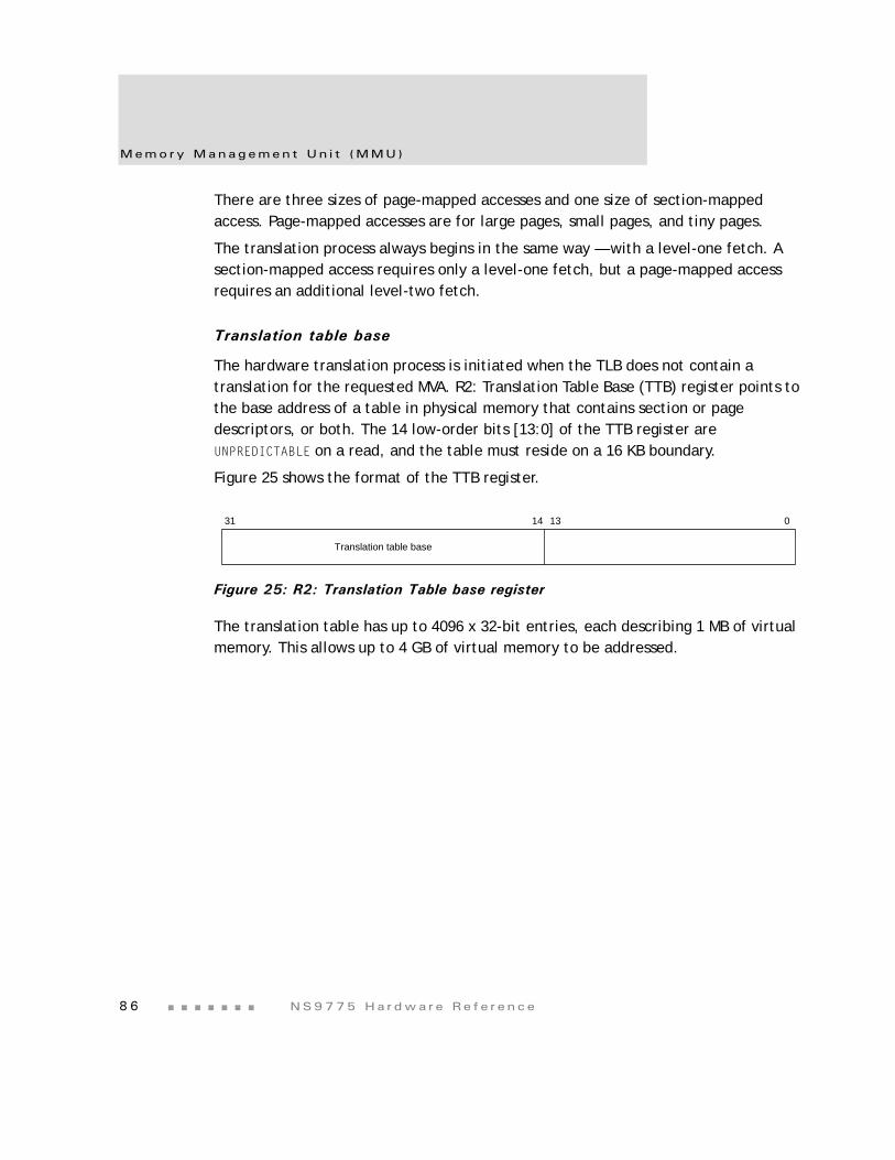
Memo ry Managemen t Un i t (MMU)
8 6 NS9775 Ha r dwa r e Re f e r ence
There are three sizes of page-mapped accesses and one size of section-mapped access. Page-mapped accesses are for large pages, small pages, and tiny pages.
The translation process always begins in the same way — with a level-one fetch. A section-mapped access requires only a level-one fetch, but a page-mapped access requires an additional level-two fetch.
Translation table base
The hardware translation process is initiated when the TLB does not contain a translation for the requested MVA. R2: Translation Table Base (TTB) register points to the base address of a table in physical memory that contains section or page descriptors, or both. The 14 low-order bits [13:0] of the TTB register are UNPREDICTABLE on a read, and the table must reside on a 16 KB boundary.
Figure 25 shows the format of the TTB register.
Figure 25: R2: Translation Table base register
The translation table has up to 4096 x 32-bit entries, each describing 1 MB of virtual memory. This allows up to 4 GB of virtual memory to be addressed.
31 014 13
Translation table base
www.d i g i . com 87
Wo rk i ng w i t h t h e CPU
Figure 26 shows the table walk process.
Figure 26: Translating page tables
Indexed bymodifiedvirtualaddressbits [31:20]
TTB baseTranslation
table Section base
Indexed bymodifiedvirtualaddressbits [19:0]
4096 entries 1 MB
Section
Large page
Indexed bymodifiedvirtualaddressbits [15:0]
Large pagebase
Coarse pagetableCoarse page
table base
Fine pagetable base
Fine pagetable
Indexed bymodifiedvirtualaddressbits [19:10]
256 entries
Indexed bymodifiedvirtualaddressbits [19:12]
1024 entries
Indexed bymodifiedvirtualaddressbits [11:0]
Indexed bymodifiedvirtualaddressbits [9:0]
64 KB
4 KB
1 KB
Tiny page
Small page
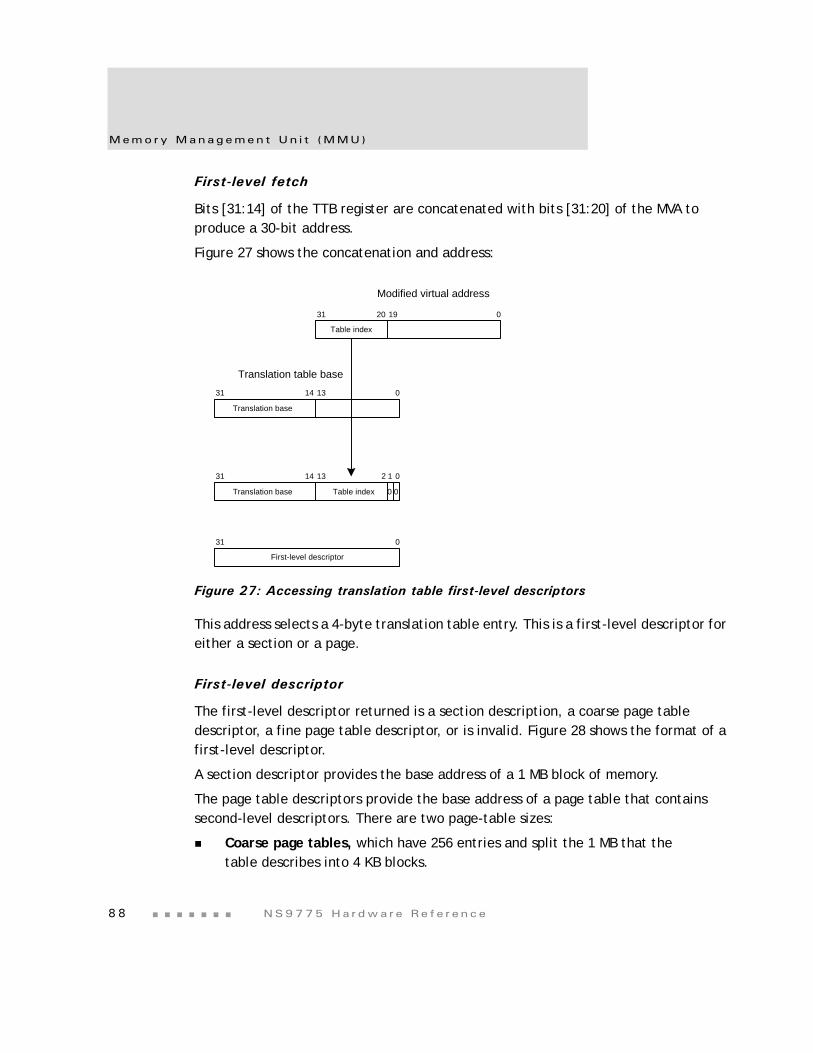
Memo ry Managemen t Un i t (MMU)
8 8 NS9775 Ha r dwa r e Re f e r ence
First-level fetch
Bits [31:14] of the TTB register are concatenated with bits [31:20] of the MVA to produce a 30-bit address.
Figure 27 shows the concatenation and address:
Figure 27: Accessing translation table first-level descriptors
This address selects a 4-byte translation table entry. This is a first-level descriptor for either a section or a page.
First-level descriptor
The first-level descriptor returned is a section description, a coarse page table descriptor, a fine page table descriptor, or is invalid. Figure 28 shows the format of a first-level descriptor.
A section descriptor provides the base address of a 1 MB block of memory.
The page table descriptors provide the base address of a page table that contains second-level descriptors. There are two page-table sizes:
Coarse page tables, which have 256 entries and split the 1 MB that the table describes into 4 KB blocks.
Modified virtual address
31 20 19 0
Table index
Translation table base31 14 13 0
Translation base
31 14 13 0
Translation base Table index 00
12
31 0
First-level descriptor
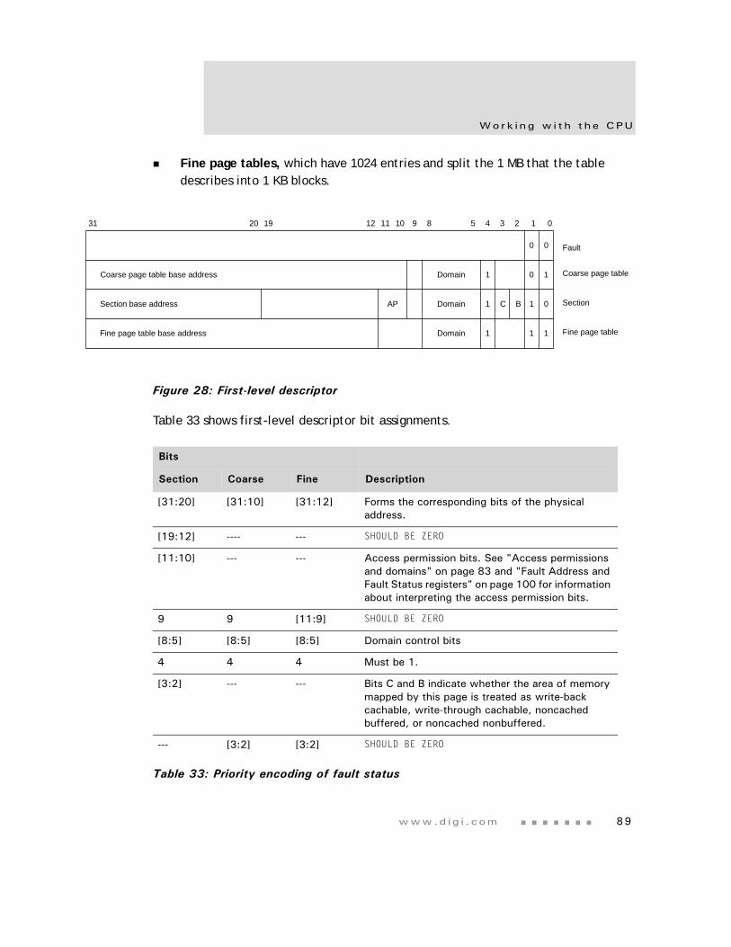
www.d i g i . com 89
Wo rk i ng w i t h t h e CPU
Fine page tables, which have 1024 entries and split the 1 MB that the table describes into 1 KB blocks.
Figure 28: First-level descriptor
Table 33 shows first-level descriptor bit assignments.
31 20 19 12 11 10 9 8 012345
0 0
0
0
1
1
1 1
1
1
1
C B
Domain
Domain
Domain
AP
Coarse page table base address
Section base address
Fine page table base address
Fault
Coarse page table
Section
Fine page table
Bits
Section Coarse Fine Description
[31:20] [31:10] [31:12] Forms the corresponding bits of the physical address.
[19:12] ---- --- SHOULD BE ZERO
[11:10] --- --- Access permission bits. See "Access permissions and domains" on page 83 and "Fault Address and Fault Status registers" on page 100 for information about interpreting the access permission bits.
9 9 [11:9] SHOULD BE ZERO
[8:5] [8:5] [8:5] Domain control bits
4 4 4 Must be 1.
[3:2] --- --- Bits C and B indicate whether the area of memory mapped by this page is treated as write-back cachable, write-through cachable, noncached buffered, or noncached nonbuffered.
--- [3:2] [3:2] SHOULD BE ZERO
Table 33: Priority encoding of fault status
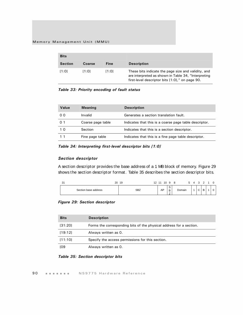
Memo ry Managemen t Un i t (MMU)
9 0 NS9775 Ha r dwa r e Re f e r ence
Section descriptor
A section descriptor provides the base address of a 1 MB block of memory. Figure 29 shows the section descriptor format. Table 35 describes the section descriptor bits.
Figure 29: Section descriptor
[1:0] [1:0] [1:0] These bits indicate the page size and validity, and are interpreted as shown in Table 34, “Interpreting first-level descriptor bits [1:0],” on page 90.
Value Meaning Description
0 0 Invalid Generates a section translation fault.
0 1 Coarse page table Indicates that this is a coarse page table descriptor.
1 0 Section Indicates that this is a section descriptor.
1 1 Fine page table Indicates that this is a fine page table descriptor.
Table 34: Interpreting first-level descriptor bits [1:0]
Bits Description
[31:20] Forms the corresponding bits of the physical address for a section.
[19:12] Always written as 0.
[11:10] Specify the access permissions for this section.
[09 Always written as 0.
Table 35: Section descriptor bits
Bits
Section Coarse Fine Description
Table 33: Priority encoding of fault status
Section base address SBZSBZ
AP Domain 1 1 0C B
1 0234589101112192031
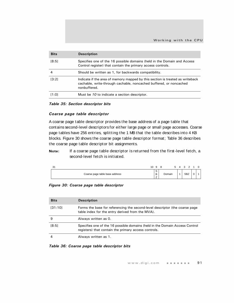
www.d i g i . com 91
Wo rk i ng w i t h t h e CPU
Coarse page table descriptor
A coarse page table descriptor provides the base address of a page table that contains second-level descriptors for either large page or small page accesses. Coarse page tables have 256 entries, splitting the 1 MB that the table describes into 4 KB blocks. Figure 30 shows the coarse page table descriptor format; Table 36 describes the coarse page table descriptor bit assignments.
Note: If a coarse page table descriptor is returned from the first-level fetch, a second-level fetch is initiated.
Figure 30: Coarse page table descriptor
[8:5] Specifies one of the 16 possible domains (held in the Domain and Access Control register) that contain the primary access controls.
4 Should be written as 1, for backwards compatibility.
[3:2] Indicate if the area of memory mapped by this section is treated as writeback cachable, write-through cachable, noncached buffered, or noncached nonbuffered.
[1:0] Must be 10 to indicate a section descriptor.
Bits Description
[31:10] Forms the base for referencing the second-level descriptor (the coarse page table index for the entry derived from the MVA).
9 Always written as 0.
[8:5] Specifies one of the 16 possible domains (held in the Domain Access Control registers) that contain the primary access controls.
4 Always written as 1.
Table 36: Coarse page table descriptor bits
Bits Description
Table 35: Section descriptor bits
Coarse page table base addressSBZ
1 0 1
1 023458931
SBZ
10
Domain
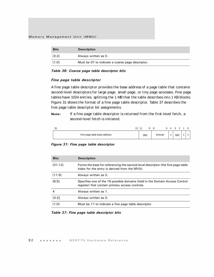
Memo ry Managemen t Un i t (MMU)
9 2 NS9775 Ha r dwa r e Re f e r ence
Fine page table descriptor
A fine page table descriptor provides the base address of a page table that contains second-level descriptors for large page, small page, or tiny page accesses. Fine page tables have 1024 entries, splitting the 1 MB that the table describes into 1 KB blocks. Figure 31 shows the format of a fine page table descriptor. Table 37 describes the fine page table descriptor bit assignments.
Note: If a fine page table descriptor is returned from the first-level fetch, a second-level fetch is initiated.
Figure 31: Fine page table descriptor
[3:2] Always written as 0.
[1:0] Must be 01 to indicate a coarse page descriptor.
Bits Description
[31:12] Forms the base for referencing the second-level descriptor (the fine page table index for the entry is derived from the MVA).
[11:9] Always written as 0.
[8:5] Specifies one of the 16 possible domains (held in the Domain Access Control register) that contain primary access controls.
4 Always written as 1.
[3:2} Always written as 0.
[1:0] Must be 11 to indicate a fine page table descriptor.
Table 37: Fine page table descriptor bits
Bits Description
Table 36: Coarse page table descriptor bits
Fine page table base address SBZ Domain 1 1 1
1 0234589111231
SBZ
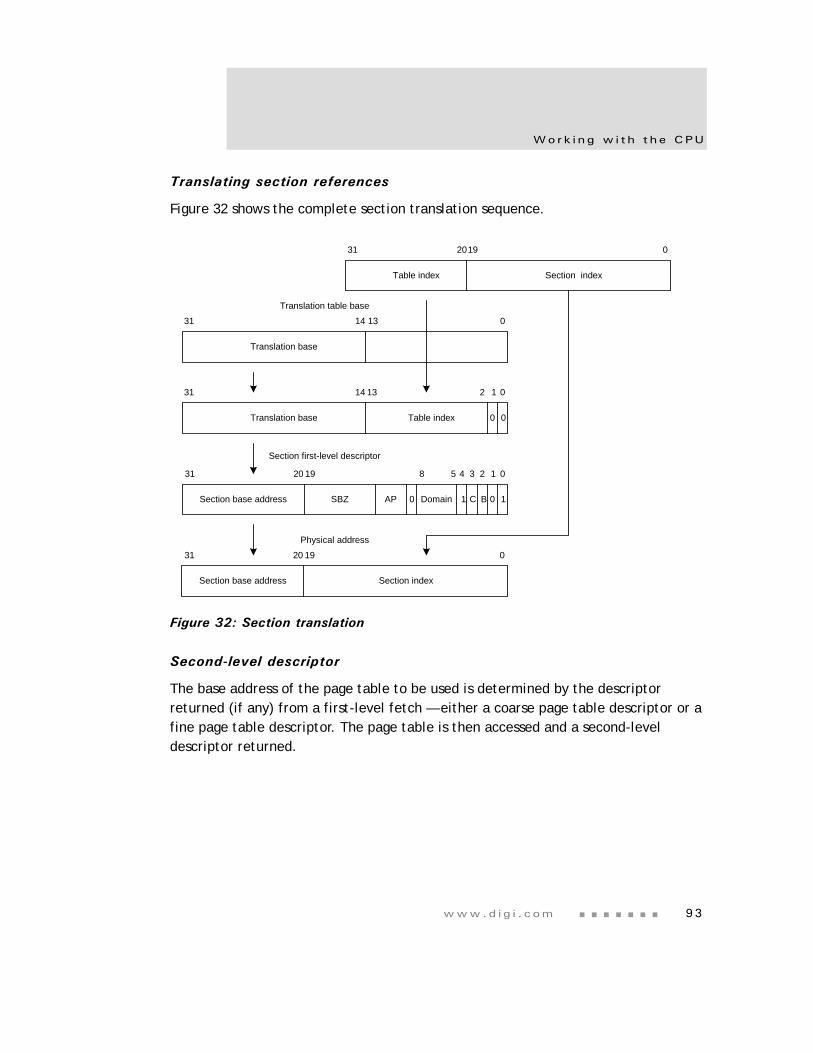
www.d i g i . com 93
Wo rk i ng w i t h t h e CPU
Translating section references
Figure 32 shows the complete section translation sequence.
Figure 32: Section translation
Second-level descriptor
The base address of the page table to be used is determined by the descriptor returned (if any) from a first-level fetch — either a coarse page table descriptor or a fine page table descriptor. The page table is then accessed and a second-level descriptor returned.
31 14 13 0
Translation base
1
Translation table base
31 14 13 0
Translation base
2
Table index 0 0
31 2019 0
Table index Section index
Section first-level descriptor
31 20 19 0
Section base address
2
0 1
1345
SBZ DomainAP 1 C B0
31 20 19 0
Section base address
Physical address
Section index
8
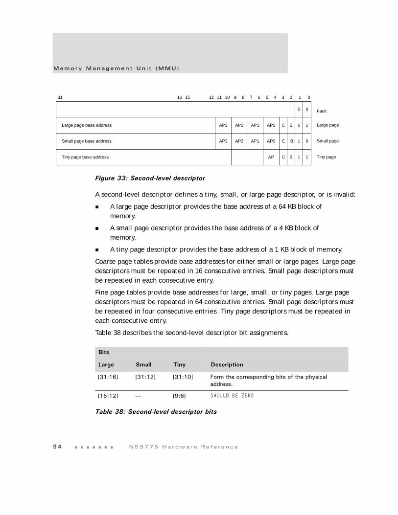
Memo ry Managemen t Un i t (MMU)
9 4 NS9775 Ha r dwa r e Re f e r ence
Figure 33: Second-level descriptor
A second-level descriptor defines a tiny, small, or large page descriptor, or is invalid:
A large page descriptor provides the base address of a 64 KB block of memory.
A small page descriptor provides the base address of a 4 KB block of memory.
A tiny page descriptor provides the base address of a 1 KB block of memory.
Coarse page tables provide base addresses for either small or large pages. Large page descriptors must be repeated in 16 consecutive entries. Small page descriptors must be repeated in each consecutive entry.
Fine page tables provide base addresses for large, small, or tiny pages. Large page descriptors must be repeated in 64 consecutive entries. Small page descriptors must be repeated in four consecutive entries. Tiny page descriptors must be repeated in each consecutive entry.
Table 38 describes the second-level descriptor bit assignments.
31 16 15 12 11 10 9 8 012345
0 0
0
0
1
1
1 1
C B
AP0Large page base address
Small page base address
Tiny page base address
7 6
C
C
B
B
AP0
AP
AP1
AP1
AP2
AP2
AP3
AP3
Fault
Large page
Small page
Tiny page
Bits
Large Small Tiny Description
[31:16] [31:12] [31:10] Form the corresponding bits of the physical address.
[15:12] --- [9:6] SHOULD BE ZERO
Table 38: Second-level descriptor bits
www.d i g i . com 95
Wo rk i ng w i t h t h e CPU
The two least significant bits of the second-level descriptor indicate the descriptor type; see Table 39.
Note: Tiny pages do not support subpage permissions and therefore have only one set of access permission bits.
Translating large page references
Figure 34 shows the complete translation sequence for a 64 KB large page.
[11:4] [11:4] [5:4] Access permission bits. See "Domain access control" on page 102 and "Fault checking sequence" on page 103 for information about interpreting the access permission bits.
[3:2] [3:2] [3:2] Indicate whether the area of memory mapped by this page is treated as write-back cachable, write-through cachable, noncached buffered, and noncached nonbuffered.
[1:0] [1:0] [1:0] Indicate the page size and validity, and are interpreted as shown in Table 39, “Interpreting page table entry bits [1:0],” on page 95.
Value Meaning Description
0 0 Invalid Generates a page translation fault.
0 1 Large page Indicates that this is a 64 KB page.
1 0 Small page Indicates that this is a 4 KB page.
1 1 Tiny page Indicates that this is a 1 KB page.
Table 39: Interpreting page table entry bits [1:0]
Bits
Large Small Tiny Description
Table 38: Second-level descriptor bits
Memo ry Managemen t Un i t (MMU)
9 6 NS9775 Ha r dwa r e Re f e r ence
Figure 34: Large page translation from a coarse page table
Because the upper four bits of the page index and low-order four bits of the coarse page table index overlap, each coarse page table entry for a large page must be duplicated 16 times (in consecutive memory locations) in the coarse page table.
31 14 13 0
Translation base
1
Translation table base
31 14 13 0
Translation base
2
Table index 0 0
31 2019 0
Table index Page index
First-level descriptor
31 0
Coarse page table base address
2
0 1
1345
Domain 1
31 0
Coarse page table base address
table index
1615 12 11
Modified virtual address
8910
12910
31 1615 121110 9 8 7 6 5 4 3 2 1 0
00L2 table index
0 1BCAP0AP1AP2AP3Page base address
Page base address
31 01615
Page index
Physical address
Second-level descriptor
www.d i g i . com 97
Wo rk i ng w i t h t h e CPU
If the large page descriptor is included in a fine page table, the high-order six bits of the page index and low-order six bits of the fine page table overlap. Each fine page table entry for a large page must be duplicated 64 times.
Translating small page references
Figure 35: Small page translation from a coarse page table
31 14 13 0
Translation base
1
Translation table base
31 14 13 0
Translation base
2
Table index 0 0
31 2019 0
Table index Page index
First-level descriptor
31 0
Coarse page table base address
2
0 1
1345
Domain 1
31 0
Coarse page table base address
Level twotable index
1211
Modified virtual address
8910
12910
31 121110 9 8 7 6 5 4 3 2 1 0
00L2 table index
01BCAP0AP1AP2AP3Page base address
Page base address
31 01211
Page index
Physical address
Second-level descriptor
Memo ry Managemen t Un i t (MMU)
9 8 NS9775 Ha r dwa r e Re f e r ence
If a small page descriptor is included in a fine page table, the upper two bits of the page index and low-order two bits of the fine page table index overlap. Each fine page table entry for a small page must be duplicated four times.
Translating tiny page references
Figure 36: Tiny page translation from a fine page table
31 14 13 0
Translation base
1
Translation table base
31 14 13 0
Translation base
2
Table index 0 0
31 2019 0
Table index Page index
First-level descriptor
31 0
Fine page table base address
2
1 1
1345
Domain 1
31 0
Fine page table base address
Level twotable index
10 9
Modified virtual address
81112
121112
31 10 9 6 5 4 3 2 1 0
00L2 table index
11BCAPPage base address
Page base address
31 010 9
Page index
Physical address
Second-level descriptor
www.d i g i . com 99
Wo rk i ng w i t h t h e CPU
Page translation involves one additional step beyond that of a section translation. The first-level descriptor is the fine page table descriptor; this points to the first-level descriptor.
Note: The domain specified in the first-level description and access permissions specified in the first-level description together determine whether the access has permissions to proceed. See "Domain access control" on page 102 for more information.
Subpages
You can define access permissions for subpages of small and large pages. If, during a page table walk, a small or large page has a different subpage permission, only the subpage being accessed is written into the TLB. For example, a 16 KB (large page) subpage entry is written into the TLB if the subpage permission differs, and a 64 KB entry is put in the TLB if the subpage permissions are identical.
When you use subpage permissions and the page entry has to be invalidated, you must invalidate all four subpages separately.
MMU faults and CPU aborts
The MMU generates an abort on these types of faults:
Alignment faults (data accesses only)
Translation faults
Domain faults
Permission faults
In addition, an external abort can be raised by the external system. This can happen only for access types that have the core synchronized to the external system:
Page walks
Noncached reads
Nonbuffered writes
Noncached read-lock-write sequence (SWP)
Alignment fault checking is enabled by the A bit in the R1: Control register. Alignment fault checking is not affected by whether the MMU is enabled. Translation, domain, and permission faults are generated only when the MMU is enabled.
Memo ry Managemen t Un i t (MMU)
1 0 0 NS9775 Ha r dwa r e Re f e r ence
The access control mechanisms of the MMU detect the conditions that produce these faults. If a fault is detected as a result of a memory access, the MMU aborts the access and signals the fault condition to the CPU core. The MMU retains status and address information about faults generated by the data accesses in the Data Fault Status register and Fault Address register (see "Fault Address and Fault Status registers" on page 100).
The MMU also retains status about faults generated by instruction fetches in the Instruction Fault Status register.
An access violation for a given memory access inhibits any corresponding external access to the AHB interface, with an abort returned to the CPU core.
Fault Address and Fault Status registers
On a data abort, the MMU places an encoded four-bit value — the fault status — along with the four-bit encoded domain number in the Data Fault Status register. Similarly, on a prefetch abort, the MMU places an encoded four-bit value along with the four-bit encoded domain number in the Instruction Fault Status register. In addition, the MVA associated with the data abort is latched into the Fault Address register. If an access violation simultaneously generates more than one source of abort, the aborts are encoded in the priority stated in Table 40. The Fault Address register is not updated by faults caused by instruction prefetches.
Priority Source Size Status Domain
Highest Alignment --- 0b00x1 Invalid
External abort on transmission First levelSecond level
0b1100
0b1110
InvalidValid
Translation Section page 0b0101
0b0111
InvalidValid
Domain Section page 0b1001
0b1011
ValidValid
Permission Section page 0b1101
0b1111
ValidValid
Lowest External abort Section page 0b1000
0b1010
ValidValid
Table 40: Priority encoding of fault status
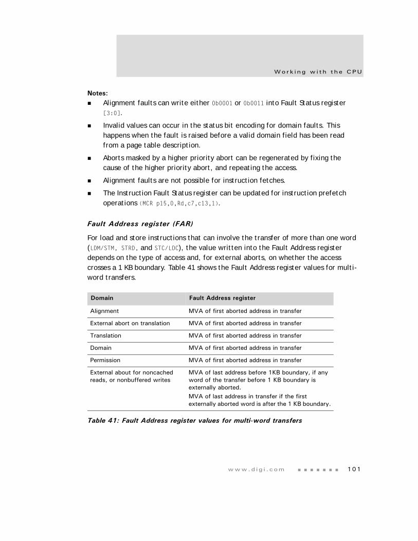
www.d i g i . com 101
Wo rk i ng w i t h t h e CPU
Notes:Alignment faults can write either 0b0001 or 0b0011 into Fault Status register [3:0].
Invalid values can occur in the status bit encoding for domain faults. This happens when the fault is raised before a valid domain field has been read from a page table description.
Aborts masked by a higher priority abort can be regenerated by fixing the cause of the higher priority abort, and repeating the access.
Alignment faults are not possible for instruction fetches.
The Instruction Fault Status register can be updated for instruction prefetch operations (MCR p15,0,Rd,c7,c13,1).
Fault Address register (FAR)
For load and store instructions that can involve the transfer of more than one word (LDM/STM, STRD, and STC/LDC), the value written into the Fault Address register depends on the type of access and, for external aborts, on whether the access crosses a 1 KB boundary. Table 41 shows the Fault Address register values for multi-word transfers.
Domain Fault Address register
Alignment MVA of first aborted address in transfer
External abort on translation MVA of first aborted address in transfer
Translation MVA of first aborted address in transfer
Domain MVA of first aborted address in transfer
Permission MVA of first aborted address in transfer
External about for noncached reads, or nonbuffered writes
MVA of last address before 1KB boundary, if any word of the transfer before 1 KB boundary is externally aborted.MVA of last address in transfer if the first externally aborted word is after the 1 KB boundary.
Table 41: Fault Address register values for multi-word transfers
Memo ry Managemen t Un i t (MMU)
1 0 2 NS9775 Ha r dwa r e Re f e r ence
Compatibility issues
To enable code to be ported easily to future architectures, it is recommended that no reliance is made on external abort behavior.
The Instruction Fault Status register is intended for debugging purposes only.
Domain access control
MMU accesses are controlled primarily through the use of domains. There are 16 domains, and each has a two-bit field to define access to it. Client users and Manager users are supported.
The domains are defined in the R3: Domain Access Control register. Figure 16, "R3: Domain Access Control register," on page 65 shows how the 32 bits of the register are allocated to define the 16 two-bit domains.
Table 42 shows how the bits within each domain are defined to specify access permissions.
Table 43 shows how to interpret the access permission (AP) bits, and how the interpretation depends on the R and S bits in the R1: Control register (see "R1: Control register," beginning on page 62).
Value Meaning Description
0 0 No access Any access generates a domain fault.
0 1 Client Accesses are checked against the access permission bits in the section or page descriptor.
1 0 Reserved Reserved. Currently behaves like no access mode.
1 1 Manager Accesses are not checked against the access permission bits, so a permission fault cannot be generated.
Table 42: Domain Access Control register, access control bits
AP S R Privileged permissions User permissions
0 0 0 0 No access No access
Table 43: Interpreting access permission (AP) bits
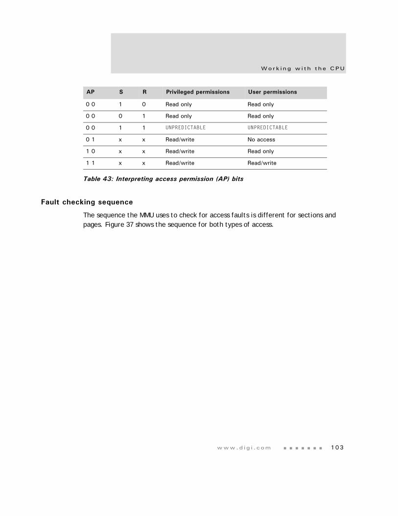
www.d i g i . com 103
Wo rk i ng w i t h t h e CPU
Fault checking sequence
The sequence the MMU uses to check for access faults is different for sections and pages. Figure 37 shows the sequence for both types of access.
0 0 1 0 Read only Read only
0 0 0 1 Read only Read only
0 0 1 1 UNPREDICTABLE UNPREDICTABLE
0 1 x x Read/write No access
1 0 x x Read/write Read only
1 1 x x Read/write Read/write
AP S R Privileged permissions User permissions
Table 43: Interpreting access permission (AP) bits
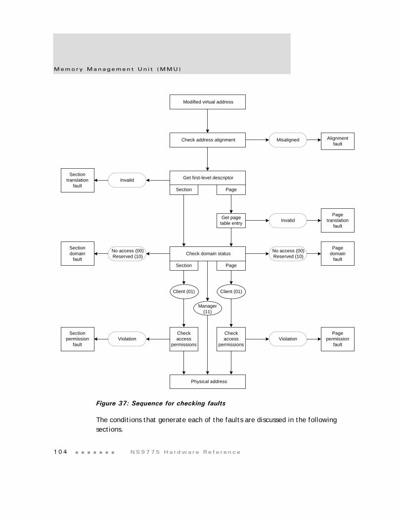
Memo ry Managemen t Un i t (MMU)
1 0 4 NS9775 Ha r dwa r e Re f e r ence
Figure 37: Sequence for checking faults
The conditions that generate each of the faults are discussed in the following sections.
Modified virtual address
Check address alignment
Get pagetable entry
Get first-level descriptor
Section Page
Check domain status
Section Page
Client (01) Client (01)
Checkaccess
permissions
Checkaccess
permissions
Physical address
Manager(11)
Misaligned Alignmentfault
Violation
Pagetranslation
fault
Pagedomain
fault
Pagepermission
fault
Invalid
No access (00)Reserved (10)
Invalid
No access (00)Reserved (10)
Sectiondomain
fault
Sectionpermission
faultViolation
Sectiontranslation
fault
www.d i g i . com 105
Wo rk i ng w i t h t h e CPU
Alignment faults
If alignment fault checking is enabled (the A bit in the R1: Control register is set; see "R1: Control register," beginning on page 62), the MMU generates an alignment fault on any data word access if the address is not word-aligned, or on any halfword access if the address is not halfword-aligned — irrespective of whether the MMU is enabled. An alignment fault is not generated on any instruction fetch or byte access.
Note: If an access generates an alignment fault, the access sequence aborts without reference to other permission checks.
Translation faults
There are two types of translation fault: section and page.
A section translation fault is generated if the level one descriptor is marked as invalid. This happens if bits [1:0] of the descriptor are both 0.
A page translation fault is generated if the level one descriptor is marked as invalid. This happens if bits [1:0] of the descriptor are both 0.
Domain faults
There are two types of domain faults: section and page.
Section: The level one descriptor holds the four-bit domain field, which selects one of the 16 two-bit domains in the Domain Access Control register. The two bits of the specified domain are then checked for access permissions as described in Table 43: "Interpreting access permission (AP) bits" on page 102. The domain is checked when the level one descriptor is returned.
Page: The level one descriptor holds the four-bit domain field, which selects one of the 16 two-bit domains in the Domain Access Control register. The two bits of the specified domain are then checked for access permissions as described in Table 43: "Interpreting access permission (AP) bits" on page 102. The domain is checked when the level one descriptor is returned.
If the specified access is either no access (00) or reserved (10), either a section domain fault or a page domain fault occurs.
Memo ry Managemen t Un i t (MMU)
1 0 6 NS9775 Ha r dwa r e Re f e r ence
Permission faults
If the two-bit domain field returns client (01), access permissions are checked as follows:
Section: If the level one descriptor defines a section-mapped access, the AP bits of the descriptor define whether the access is allowed, per Table 43: "Interpreting access permission (AP) bits" on page 102. The interpretation depends on the setting of the S and R bits (see "R1: Control register," beginning on page 62). If the access is not allowed, a section permission fault is generated.
Large page or small page: If the level one descriptor defines a page-mapped access and the level two descriptor is for a large or small page, four access permission fields (AP3 to AP0) are specified, each corresponding to one quarter of the page.
For small pages, AP3 is selected by the top 1 KB of the page and AP0 is selected by the bottom 1 KB of the page.
For large pages, AP3 is selected by the top 16 KB of the page and AP0 is selected by the bottom 16 KB of the page. The selected AP bits are then interpreted in the same way as for a section (see Table 43: "Interpreting access permission (AP) bits" on page 102).
The only difference is that the fault generated is a page permission fault.
Tiny page: If the level one descriptor defines a page-mapped access and the level two descriptor is for a tiny page, the AP bits of the level one descriptor define whether the access is allowed in the same way as for a section. The fault generated is a page permission fault.
External aborts
In addition to MMU-generated aborts, external aborts cam be generated for certain types of access that involve transfers over the AHB bus. These aborts can be used to flag errors on external memory accesses. Not all accesses can be aborted in this way, however.
These accesses can be aborted externally:
Page walks
Noncached reads
www.d i g i . com 107
Wo rk i ng w i t h t h e CPU
Nonbuffered writes
Noncached read-lock-write (SWP) sequence
For a read-lock-write (SWP) sequence, the write is always attempted if the read externally aborts.
A swap to an NCB region is forced to have precisely the same behavior as a swap to an NCNB region. This means that the write part of a swap to an NCB region can be aborted externally.
Enabling the MMU
Before enabling the MMU using the R1: Control register (see page 62), you must perform these steps:
1 Program the R2: Translation Table Base register (see page 65) and the R3: Domain Access Control register (see page 65).
2 Program first-level and second-level page tables as required, ensuring that a valid translation table is placed in memory at the location specified by the Translation Table Base register.
When these steps have been performed, you can enable the MMU by setting R1: Control register bit 0 (the M bit) to high.
Care must be taken if the translated address differs from the untranslated address, because several instructions following the enabling of the MMU might have been prefetched with MMU off (VA=MVA=PA). If this happens, enabling the MMU can be considered as a branch with delayed execution. A similar situation occurs when the MMU is disabled. Consider this code sequence:
MRC p15, 0, R1, c1, C0, 0 ; Read control register
ORR R1, #0x1 ; Set M bit
MCR p15, 0,R1,C1, C0,0 ; Write control register and enable MMU
Fetch Flat
Fetch Flat
Fetch Translated
Note: Because the same register (R1: Control register) controls the enabling of ICache, DCache, and the MMU, all three can be enabled using a single MCR instruction.
Memo ry Managemen t Un i t (MMU)
1 0 8 NS9775 Ha r dwa r e Re f e r ence
Disabling the MMU
Clear bit 0 (the M bit) in the R1: Control register to disable the MMU.
Note: If the MMU is enabled, then disabled, then subsequently re-enabled, the contents of the TLB are preserved. If these are now invalid, the TLB must be invalidated before re-enabling the MMU (see "R8:TLB Operations register" on page 72).
TLB structure
The MMU runs a single unified TLB used for both data accesses and instruction fetches. The TLB is divided into two parts:
An eight-entry fully-associative part used exclusively for holding locked down TLB entries.
A set-associative part for all other entries.
Whether an entry is placed in the set-associative part or lockdown part of the TLB depends on the state of the TLB Lockdown register when the entry is written into the TLB (see "R10: TLB Lockdown register" on page 77).
When an entry has been written into the lockdown part of the TLB, it can be removed only by being overwritten explicitly or, when the MVA matches the locked down entry, by an MVA-based TLB invalidate operation.
The structure of the set-associative part of the TLB does not form part of the programmer’s model for the ARM926EJ-S processor. No assumptions must be made about the structure, replacement algorithm, or persistence of entries in the set-associative part — specifically:
Any entry written into the set-associative part of the TLB can be removed at any time. The set-associative part of the TLB must be considered as a temporary cache of translation/page table information. No reliance must be placed on an entry residing or not residing in the set-associative TLB unless that entry already exists in the lockdown TLB. The set-associative part of the TLB can contain entries that are defined in the page tables but do not correspond to address values that have been accessed since the TLB was invalidated.
The set-associative part of the TLB must be considered as a cache of the underlying page table, where memory coherency must be maintained at all
www.d i g i . com 109
Wo rk i ng w i t h t h e CPU
times. To guarantee coherency if a level one descriptor is modified in main memory, either an invalidate-TLB or Invalidate-TLB-by-entry operation must be used to remove any cached copies of the level one descriptor. This is required regardless of the type of level one descriptor (section, level two page reference, or fault).
If any of the subpage permissions for a given page are different, each of the subpages are treated separately. To invalidate all entries associated with a page with subpage permissions, four MVA-based invalidate operations are required — one for each subpage.
Caches and write buffer
The ARM926EJ-S processor includes an instruction cache (ICache), data cache (DCache), and write buffer. The size of the caches can be from 4 KB to 128 KB, in power of two increments.
Cache features
The caches are virtual index, virtual tag, addressed using the modified virtual address (MVA). This avoids cache cleaning and/or invalidating on context switch.
The caches are four-way set associative, with a cache line length of eight words per line (32 bytes per line), and with two dirty bits in the DCache.
The DCache supports write-through and write-back (copyback) cache operations, selected by memory region using the C and B bits in the MMU translation tables.
The caches support allocate on read-miss. The caches perform critical-word first cache refilling.
The caches use pseudo-random or round-robin replacement, selected by the RR bit in R1: Control register.
Cache lockdown registers enable control over which cache ways are used for allocation on a linefill, providing a mechanism for both lockdown and controlling cache pollution.
Caches and w r i t e bu f f e r
1 1 0 NS9775 Ha r dwa r e Re f e r ence
The DCache stores the Physical Address Tag (PA tag) corresponding to each DCache entry in the tag RAM for use during cache line write-backs, in addition to the virtual address tag stored in the tag RAM. This means that the MMU is not involved in DCache write-back operations, which removes the possibility of TLB misses to the write-back address.
Cache maintenance operations provide efficient invalidation of:
– The entire DCache or ICache
– Regions of the DCache or ICache
– Regions of virtual memory
Cache maintenance operations also provide for efficient cleaning and invalidation of:
– The entire DCache
– Regions of the DCache
– Regions of virtual memory
The latter allows DCache coherency to be efficiently maintained when small code changes occur; for example, for self-modifying code and changes to exception vectors.
Write buffer
The write buffer is used for all writes to a noncachable bufferable region, write-through region, and write misses to a write-back region. A separate buffer is incorporated in the DCache for holding write-back data for cache line evictions or cleaning of dirty cache lines.
The main write buffer has a 16-word data buffer and a four-address buffer.
The DCache write-back buffer has eight data word entries and a single address entry.
The MCR drain write buffer instruction enables both write buffers to be drained under software control.
The MCR wait -for-interrupt causes both write buffers to be drained, and the ARM926EJ-S processor to be put into low-power state until an interrupt occurs.
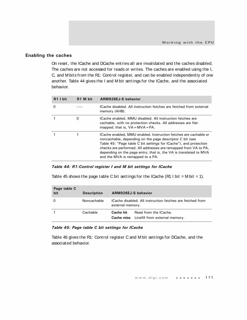
www.d i g i . com 111
Wo rk i ng w i t h t h e CPU
Enabling the caches
On reset, the ICache and DCache entries all are invalidated and the caches disabled. The caches are not accessed for reads or writes. The caches are enabled using the I, C, and M bits from the R1: Control register, and can be enabled independently of one another. Table 44 gives the I and M bit settings for the ICache, and the associated behavior.
Table 45 shows the page table C bit settings for the ICache (R1 I bit = M bit = 1).
Table 46 gives the R1: Control register C and M bit settings for DCache, and the associated behavior.
R1 I bit R1 M bit ARM926EJ-S behavior
0 ----- ICache disabled. All instruction fetches are fetched from external memory (AHB).
1 0 ICache enabled, MMU disabled. All instruction fetches are cachable, with no protection checks. All addresses are flat-mapped; that is, VA=MVA=PA.
1 1 ICache enabled, MMU enabled. Instruction fetches are cachable or noncachable, depending on the page descriptor C bit (see Table 45: "Page table C bit settings for ICache"), and protection checks are performed. All addresses are remapped from VA to PA, depending on the page entry; that is, the VA is translated to MVA and the MVA is remapped to a PA.
Table 44: R1:Control register I and M bit settings for ICache
Page table C bit Description ARM926EJ-S behavior
0 Noncachable ICache disabled. All instruction fetches are fetched from external memory.
1 Cachable Cache hit Read from the ICache.Cache miss Linefill from external memory.
Table 45: Page table C bit settings for ICache
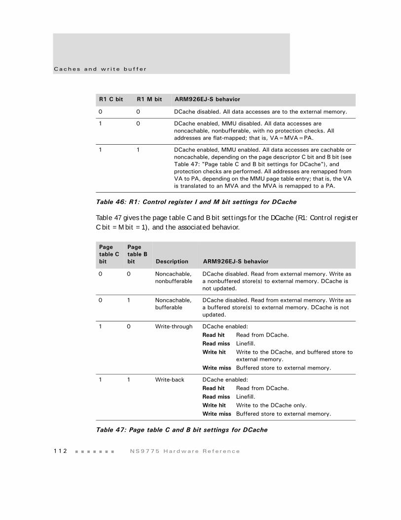
Caches and w r i t e bu f f e r
1 1 2 NS9775 Ha r dwa r e Re f e r ence
Table 47 gives the page table C and B bit settings for the DCache (R1: Control register C bit = M bit = 1), and the associated behavior.
R1 C bit R1 M bit ARM926EJ-S behavior
0 0 DCache disabled. All data accesses are to the external memory.
1 0 DCache enabled, MMU disabled. All data accesses are noncachable, nonbufferable, with no protection checks. All addresses are flat-mapped; that is, VA=MVA=PA.
1 1 DCache enabled, MMU enabled. All data accesses are cachable or noncachable, depending on the page descriptor C bit and B bit (see Table 47: "Page table C and B bit settings for DCache"), and protection checks are performed. All addresses are remapped from VA to PA, depending on the MMU page table entry; that is, the VA is translated to an MVA and the MVA is remapped to a PA.
Table 46: R1: Control register I and M bit settings for DCache
Page table C bit
Page table B bit Description ARM926EJ-S behavior
0 0 Noncachable, nonbufferable
DCache disabled. Read from external memory. Write as a nonbuffered store(s) to external memory. DCache is not updated.
0 1 Noncachable, bufferable
DCache disabled. Read from external memory. Write as a buffered store(s) to external memory. DCache is not updated.
1 0 Write-through DCache enabled:Read hit Read from DCache.Read miss Linefill.Write hit Write to the DCache, and buffered store to
external memory.Write miss Buffered store to external memory.
1 1 Write-back DCache enabled:Read hit Read from DCache.Read miss Linefill.Write hit Write to the DCache only.Write miss Buffered store to external memory.
Table 47: Page table C and B bit settings for DCache
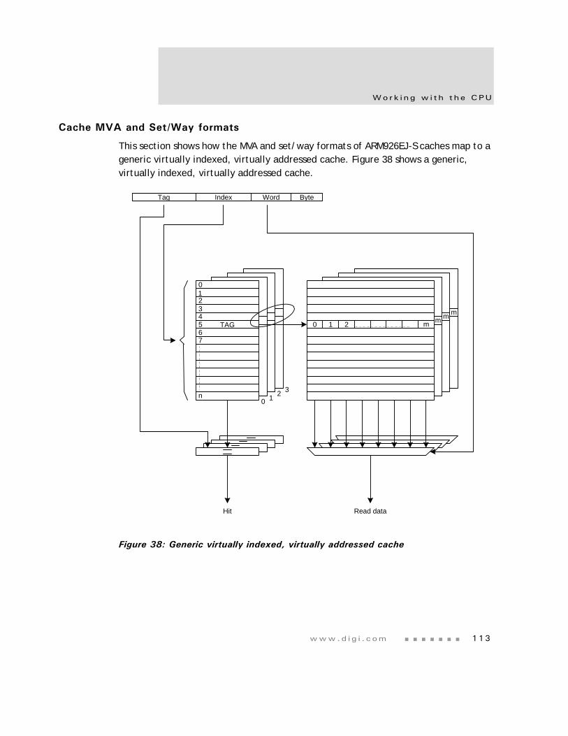
www.d i g i . com 113
Wo rk i ng w i t h t h e CPU
Cache MVA and Set/Way formats
This section shows how the MVA and set/way formats of ARM926EJ-S caches map to a generic virtually indexed, virtually addressed cache. Figure 38 shows a generic, virtually indexed, virtually addressed cache.
Figure 38: Generic virtually indexed, virtually addressed cache
0
01234567
n
TAG
1 2 3
0 1 2 m m m m
Hit Read data
Tag Index Word Byte
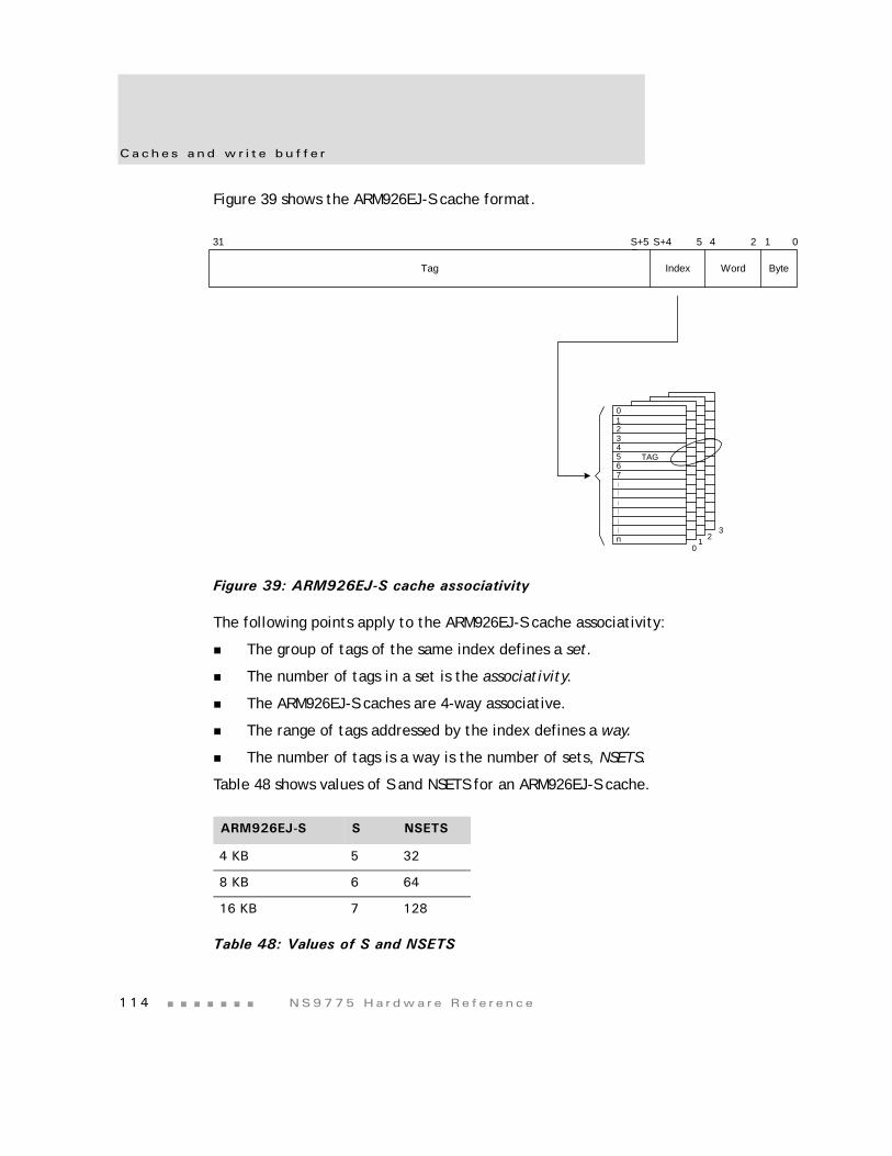
Caches and w r i t e bu f f e r
1 1 4 NS9775 Ha r dwa r e Re f e r ence
Figure 39 shows the ARM926EJ-S cache format.
Figure 39: ARM926EJ-S cache associativity
The following points apply to the ARM926EJ-S cache associativity:
The group of tags of the same index defines a set.
The number of tags in a set is the associativity.
The ARM926EJ-S caches are 4-way associative.
The range of tags addressed by the index defines a way.
The number of tags is a way is the number of sets, NSETS.
Table 48 shows values of S and NSETS for an ARM926EJ-S cache.
ARM926EJ-S S NSETS
4 KB 5 32
8 KB 6 64
16 KB 7 128
Table 48: Values of S and NSETS
01234567
n
TAG
1 2
31 0
Tag Index Word Byte
S+5 1S+4 245
0
3
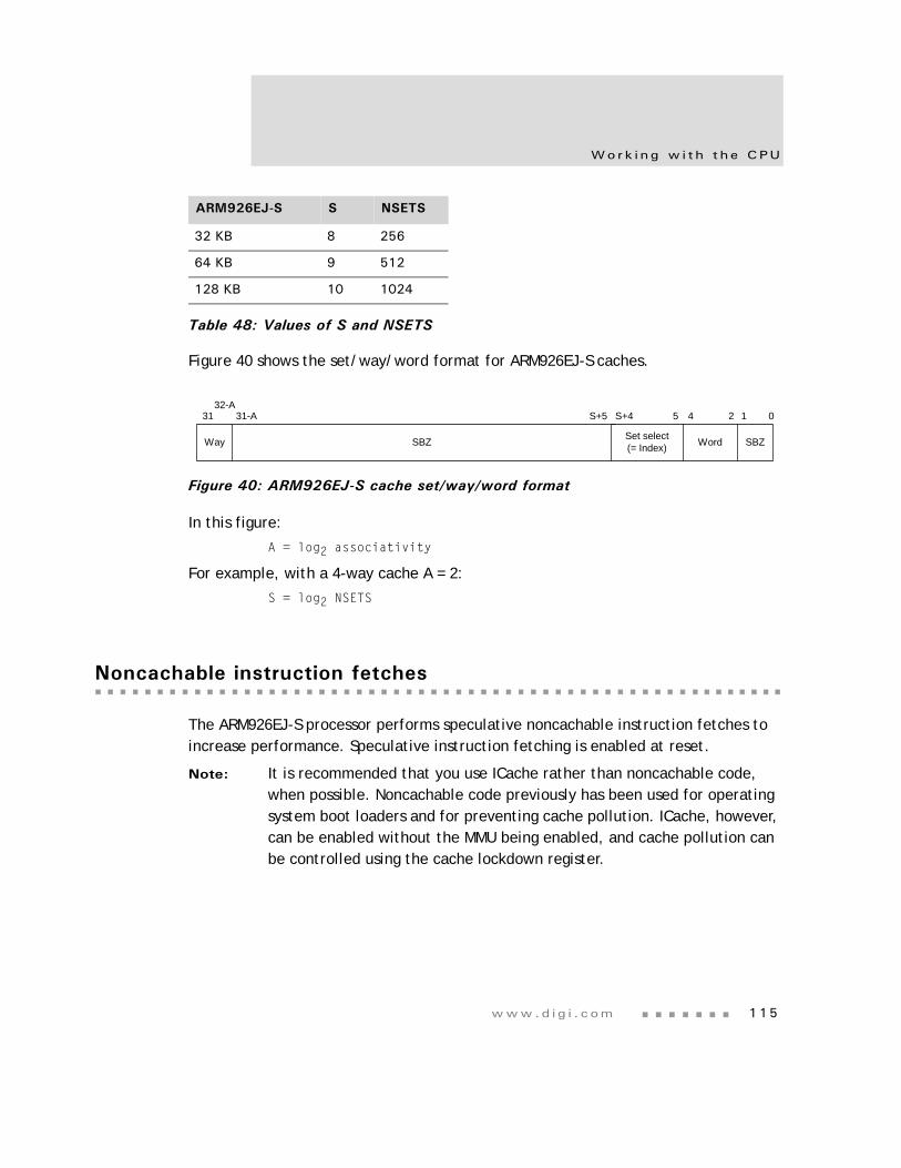
www.d i g i . com 115
Wo rk i ng w i t h t h e CPU
Figure 40 shows the set/way/word format for ARM926EJ-S caches.
Figure 40: ARM926EJ-S cache set/way/word format
In this figure:
A = log2 associativity
For example, with a 4-way cache A = 2:
S = log2 NSETS
Noncachable instruction fetches
The ARM926EJ-S processor performs speculative noncachable instruction fetches to increase performance. Speculative instruction fetching is enabled at reset.
Note: It is recommended that you use ICache rather than noncachable code, when possible. Noncachable code previously has been used for operating system boot loaders and for preventing cache pollution. ICache, however, can be enabled without the MMU being enabled, and cache pollution can be controlled using the cache lockdown register.
32 KB 8 256
64 KB 9 512
128 KB 10 1024
ARM926EJ-S S NSETS
Table 48: Values of S and NSETS
31 0
Way
31-A32-A
S+5 S+4 5 4 2 1
SBZ SBZWordSet select(= Index)
Noncachab l e i n s t r u c t i o n f e t c he s
1 1 6 NS9775 Ha r dwa r e Re f e r ence
Self-modifying code
A four-word buffer holds speculatively fetched instructions. Only sequential instructions are fetched speculatively; if the ARM926EJ-S issues a nonsequential instruction fetch, the contents of the buffer are discarded (flushed). In situations on which the contents of the prefetch buffer might become invalid during a sequence of sequential instruction fetches by the processor core (for example, turning the MMU on or off, or turning on the ICache), the prefetch buffer also is flushed. This avoids the necessity of performing an explicit Instruction Memory Barrier (IMB) operation, except when self-modifying code is used. Because the prefetch buffer is flushed when the ARM926EJ-S core issues a nonsequential instruction fetch, a branch instruction (or equivalent) can be used to implement the required IMB behavior, as shown in this code sequence:
LDMIA R0,{R1-R5} ; load code sequence into R1-R5
ADR R0,self_mod_code
STMIA R0,{R1-R5} ; store code sequence (nonbuffered region)
B self_mod_code ; branch to modified code
self_mod_code:
This IMB application applies only to the ARM926EJ-S processor running code from a noncachable region of memory. If code is run from a cachable region of memory, or a different device is used, a different IMB implementation is required. IMBs are discussed in "Instruction Memory Barrier," beginning on page 117.
AHB behavior
If instruction prefetching is disabled, all instruction fetches appear on the AHB interface as single, nonsequential fetches.
If prefetching is enabled, instruction fetches appear either as bursts of four instructions or as single, nonsequential fetches. No speculative instruction fetching is done across a 1 KB boundary.
All instruction fetches, including those made in Thumb state, are word transfers (32 bits). In Thumb state, a single-word instruction fetch reads two Thumb instructions and a four-word burst reads eight instructions.
www.d i g i . com 117
Wo rk i ng w i t h t h e CPU
Instruction Memory Barrier
Whenever code is treated as data — for example, self-modifying code or loading code into memory — a sequence of instructions called an instruction memory barrier (IMB) operation must be used to ensure consistency between the data and instruction streams processed by the ARM926EJ-S processor.
Usually the instruction and data streams are considered to be completely independent by the ARM926EJ-S processor memory system, and any changes in the data side are not automatically reflected in the instruction side. For example, if code is modified in main memory, ICache may contain stale entries. To remove these stale entries, part of all of the ICache must be invalidated.
IMB operation
Use this procedure to ensure consistency between data and instruction sides:
1 Clean the DCache. If the cache contains cache lines corresponding to write-back regions of memory, it might contain dirty entries. These entries must be cleaned to make external memory consistent with the DCache. If only a small part of the cache has to be cleaned, it can be done by using a sequence of clean DCache single entry instructions. If the entire cache has to be cleaned, you can use the test and clean operation (see "R7: Cache Operations register," beginning on page 68).
2 Drain the write buffer. Executing a drain write buffer causes the ARM926EJ-S core to wait until outstanding buffered writes have completed on the AHB interface. This includes writes that occur as a result of data being written back to main memory because of clean operations, and data for store instructions.
3 Synchronize data and instruction streams in level two AHB systems. The level two AHB subsystem might require synchronization between data and instruction sides. It is possible for the data and instruction AHB masters to be attached to different AHB subsystems. Even if both masters are present on the same bus, some form of separate ICache might exist for performance reasons; this must be invalidated to ensure consistency.
The process of synchronizing instructions and data in level two memory must be invoked using some form of fully blocking operation, to ensure that the end of the operation can be determined using software. It is
I n s t r u c t i o n Memo ry Ba r r i e r
1 1 8 NS9775 Ha r dwa r e Re f e r ence
recommended that either a nonbuffered store (STR) or a noncached load (LDR) be used to trigger external synchronization.
4 Invalidate the cache. The ICache must be invalidated to remove any stale copies of instructions that are no longer valid. If the ICache is not being used, or the modified regions are not in cachable areas of memory, this step might not be required.
5 Flush the prefetch buffer. To ensure consistency, the prefetch buffer should be flushed before self-modifying code is executed (see "Self-modifying code" on page 116).
Sample IMB sequences
These sequences correspond to steps 1–4 in "IMB operation."
clean loop
MRC p15, 0, r15, c7, c10, 3; clean entire dcache using test and clean
BNE clean_loop
MRC p15, 0, r0, c7, c10, 4 ; drain write buffer
STR rx,[ry] ; nonbuffered store to signal L2 world to
; synchronize
MCR p15, 0, r0, c7, c5, 0 ; invalidate icache
This next sequence illustrates an IMB sequence used after modifying a single instruction (for example, setting a software breakpoint), with no external synchronization required:
STR rx,[ry] ; store that modifies instruction at address ry
MCR p15, 0, ry, c7, c10, 1 ; clean dcache single entry (MVA)
MCR p15, 0, r0, c7, c10, 4 ; drain write buffer
MCR p15, 0, ry, c7, c5, 1 ; invalidate icache single entry (MVA)
119
System Control ModuleC H A P T E R 4
The System Control Module configures and oversees system operations for the NS9775, and defines both the NS9775 AHB arbiter system and system memory address space.
Sys t em Con t r o l Modu l e f e a t u r e s
1 2 0 NS9775 Ha r dwa r e Re f e r ence
System Control Module features
The System Control Module uses the following to configure and maintain NS9775 system operations:
AHB arbiter system
System-level address decoding
18 programmable timers
– Watchdog timer
– Bus monitor timer for the system bus (a second bus monitor timer, for peripheral devices, is discussed in the BBus Bridge chapter)
– 16 general purpose timers/counters
Interrupt controller
Multiple configuration and status registers
System Sleep/Wake-up processor
Bus interconnection
The AMBA AHB bus protocol uses a central multiplexor interconnection scheme. All bus masters generate the address and control signals that indicate the transfer that the bus masters want to perform. The arbiter determines which master has its address and control signals routed to all slaves. A central decoder is required to control the read data and response multiplexor, which selects the appropriate signals from the slave that is involved in the transfer.
System bus arbiter
The bus arbitration mechanism ensures that only one bus master has access to the system bus at any time. If you are using a system in which bus bandwidth allocation is critical, you must be sure that your worst-case bus bandwidth allocation goals can be
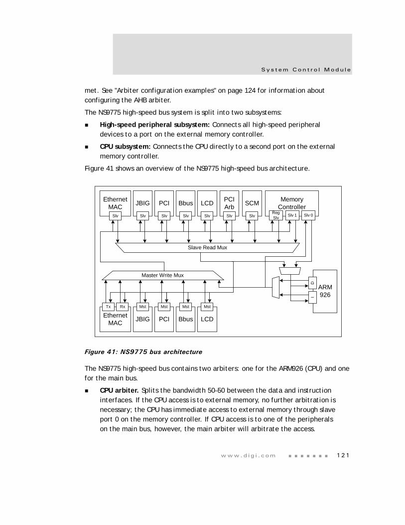
www.d i g i . com 121
Sys t em Con t r o l Modu l e
met. See "Arbiter configuration examples" on page 124 for information about configuring the AHB arbiter.
The NS9775 high-speed bus system is split into two subsystems:
High-speed peripheral subsystem: Connects all high-speed peripheral devices to a port on the external memory controller.
CPU subsystem: Connects the CPU directly to a second port on the external memory controller.
Figure 41 shows an overview of the NS9775 high-speed bus architecture.
Figure 41: NS9775 bus architecture
The NS9775 high-speed bus contains two arbiters: one for the ARM926 (CPU) and one for the main bus.
CPU arbiter. Splits the bandwidth 50–50 between the data and instruction interfaces. If the CPU access is to external memory, no further arbitration is necessary; the CPU has immediate access to external memory through slave port 0 on the memory controller. If CPU access is to one of the peripherals on the main bus, however, the main arbiter will arbitrate the access.
ARM926I
D
EthernetMAC
Slv
JBIG
Slv
PCI
Slv
Bbus
Slv
LCD
Slv
MemoryController
RegSlv Slv 1
EthernetMAC
Tx Rx
JBIG
Mst
PCI
Mst
Bbus
Mst
LCD
Mst
Master Write Mux
Slave Read Mux
PCIArbSlv
SCM
Slv Slv 0
Sys t em bus a r b i t e r
1 2 2 NS9775 Ha r dwa r e Re f e r ence
Main arbiter. Contains a 16-entry Bus Request Configuration (BRC) register. Each BRC entry represents a bus request and grant channel. Each request/grant channel can be assigned to only one bus master at a time. Each bus master can be connected to multiple request/grant channels simultaneously, however, depending on the bus bandwidth requirement of that master.
Each request/grant channel has a two-bit Bandwidth Reduction Field (BRF) to determine how often each channel can arbitrate for the system bus — 100%, 75%, 50%, or 25%. A BRF value of 25%, for example, causes a channel to be skipped every 3 or 4 cycles. The BRC gates the bus requesting signals going into a 16-entry Bus Request register (BRR). As a default, unassigned channels in the BRC block the corresponding BRR entries from being set by any bus request signals. On powerup, only the CPU is assigned to one of the channels with 100% bandwidth strength as the default setting.
How the bus arbiter works
1 The arbiter evaluates the Bus Request register at every bus clock until one or more bus requests are registered.
2 The arbiter stops evaluating the Bus Request register until a bus grant is issued for the previous evaluation cycle.
3 The arbiter grants the bus to requesting channels, in a round-robin manner, at the rising clock edge of the last address issued for the current transaction (note that each transaction may have multiple transfers), when a SPLIT response is sampled by the arbiter, or when the bus is idling.
4 Each master samples the bus grant signal (hgrant_x) at the end of the current transfer, as indicated by the hready signal. The bus master takes ownership of the bus at this time.
5 The arbiter updates the hmaster [3:0] signals at the same time to indicate the current bus master and to enable the new master’s address and control signals to the system bus.
See your AMBA standards documentation for detailed information and illustrations of AMBA AHB transactions.
www.d i g i . com 123
Sys t em Con t r o l Modu l e
Ownership
Ownership of the data bus is delayed from ownership of the address/control bus. When hready indicates that a transfer is complete, the master that owns the address/control bus can use the data bus — and continues to own that data bus — until the transaction completes.
Note: If a master is assigned more than one request/grant channel, these channels need to be set and reset simultaneously to guarantee that a non-requesting master will not occupy the system bus.
Locked bus sequence
The arbiter observes the hlock_x signal from each master to allow guaranteed back-to-back cycles, such as read-modified-write cycles. The arbiter ensures that no other bus masters are granted the bus until the locked sequence has completed. To support SPLIT or RETRY transfers in a locked sequence, the arbiter retains the bus master as granted for an additional transfer to ensure that the last transfer in the locked sequence completed successfully.
If the master is performing a locked transfer and the slave issues a split response, the master continues to be granted the bus until the slave finishes the SPLIT response. (This situation degrades AHB performance.)
Relinquishing the bus
When the current bus master relinquishes the bus, ownership is granted to the next requester.
If there are no new requesters, ownership is granted to a dummy default master. The default master must perform IDLE transfers to keep the arbiter alive.
Bus parking must be maintained if other masters are waiting for SPLIT transfers to complete.
If the bus is granted to a default master and continues to be in the IDLE state longer than a specified period of time, an AHB bus arbiter timeout is generated (see "AHB bus error monitoring" on page 127). An AHB bus arbiter timeout can be configured to interrupt the CPU or to reset the chip.
Sys t em bus a r b i t e r
1 2 4 NS9775 Ha r dwa r e Re f e r ence
SPLIT transfers
A SPLIT transfer occurs when a slave is not ready to perform the transfer. The slave splits, or masks, its master, taking away the master’s bus ownership and allowing other masters to perform transactions until the slave has the appropriate resources to perform its master’s transaction.
The bus arbiter supports SPLIT transfers. When a SPLIT response is issued by a slave, the current master is masked for further bus requesting until a corresponding hsplit_x[15:0] signal is issued by the slave indicating that the slave is ready to complete the transfer. The arbiter uses the hsplit_x[15:0] signals to unmask the corresponding master, and treats the master as the highest-priority requester for the immediate next round of arbitration. The master eventually is granted access to the bus to try the transfer again.
Note: The arbiter automatically blocks bus requests with addresses directed at a “SPLITting” slave until that SPLIT transaction is completed.
Arbiter configuration examples
These examples show how to configure the AHB arbiter to guarantee bandwidth to a given master. These are the conditions in this example:
5 AHB masters — Ethernet Rx, Ethernet Tx, PCI, BBus, and LCD.
Memory clock frequency — 100 MHz (this is the AHB clock frequency).
Average access time per 32-byte memory access — 16 clock cycles.
The ARM926EJ-S is guaranteed one-half the total memory bandwidth.
In these examples, the bandwidth for each master can be calculated using this formula:
Bandwidth per master:
= [(100MHz/2) / (16 clock cycles per access x 5 masters)] x 32 bytes
= 20 Mbytes/master
The factor 100MHz/2 is given due to the ARM926EJ-S guarantee of one-half the total memory bandwidth. If the ARM926EJ-S consumes less than the guaranteed memory bandwidth, however, the unused bandwidth will be shared by the other masters.
Note: The worst case scenario is that there are 100 Mbytes total to be split by all 5 masters.
www.d i g i . com 125
Sys t em Con t r o l Modu l e
Example 1
Since the 20 Mbyte per master guarantee meets the requirements of all masters, the AHB arbiter will be programmed as follows:
BRC0[31:24] = 8’b1_0_00_0000 channel enabled, 100%, ARM926EJ-S
BRC0[23:16] = 8’b1_0_00_0001 channel enabled, 100%, Ethernet Rx
BRC0[15:8] = 8’b1_0_00_0000 channel enabled, 100%, ARM926EJ-S
BRC0[7:0] = 8’b1_0_00_0010 channel enabled, 100%, Ethernet Tx
BRC1[31:24] = 8’b1_0_00_0000 channel enabled, 100%, ARM926EJ-S
BRC1[23:16] = 8’b1_0_00_0100 channel enabled, 100%, PCI
BRC1[15:8] = 8’b1_0_00_0000 channel enabled, 100%, ARM926EJ-S
BRC1[7:0] = 8’b1_0_00_0101 channel enabled, 100%, BBus
BRC2[31:24] = 8’b1_0_00_0000 channel enabled, 100%, ARM926EJ-S
BRC2[23:16] = 8’b1_0_00_0100 channel enabled, 100%, LCD
BRC2[15:8] = 8’b0_0_00_0000 channel disabled
BRC2[7:0] = 8’b0_0_00_0000 channel disabled
BRC3[31:24] = 8’b0_0_00_0000 channel disabled
BRC3[23:16] = 8’b0_0_00_0000 channel disabled
BRC3[15:8] = 8’b0_0_00_0000 channel disabled
BRC[7:0] = 8’b0_0_00_0000 channel disabled
Example 2
In this example, the LCD master needs more than 20 Mbytes and the other masters need less than 20 Mbytes. These are the new requirements:
Ethernet Rx — 12.5 Mbytes
Ethernet Tx — 12.5 Mbytes
PCI — 16 Mbytes
BBus — 4 Mbytes
LCD — 25 Mbytes
Total — 70 Mbytes
This configuration is possible because the total bandwidth is less than the 100 Mbytes available. The LCD master will be configured to have two arbiter slots, resulting in a total of 6 masters.
Sys t em bus a r b i t e r
1 2 6 NS9775 Ha r dwa r e Re f e r ence
The available bandwidth per master is calculated using this formula:
Bandwidth per master:
= [(100MHz/2) / (16 clock cycles per access x 6 masters)] x 32 bytes
= 16.667 Mbytes/master
If the LCD is configured for two arbiter channel slots, then, there are 33.334 Mbytes available, which is greater than the 25 Mbytes required. Each of the other masters have 16.667 Mbytes available, which is more than enough to meet their requirements.
Note: When assigning two arbiter channel slots to a master, the slot assignments should be spaced equally.
The AHB arbiter will be programmed as follows:
BRC0[31:24] = 8’b1_0_00_0000 channel enabled, 100%, ARM926EJ-S
BRC0[23:16] = 8’b1_0_00_0001 channel enabled, 100%, Ethernet Rx
BRC0[15:8] = 8’b1_0_00_0000 channel enabled, 100%, ARM926EJ-S
BRC0[7:0] = 8’b1_0_00_0010 channel enabled, 100% Ethernet Tx
BRC1[31:24] = 8’b1_0_00_0000 channel enabled, 100%, ARM926EJ-S
BRC1[23:16] = 8’b1_0_00_0110 channel enabled, 100%, LCD first slot
BRC1[15:8] = 8’b1_0_00_0000 channel enabled, 100%, ARM926EJ-S
BRC1[7:0] = 8’b1_0_00_0100 channel enabled, 100%, PCI
BRC2[31:24] = 8’b1_0_00_0000 channel enabled, 100%, ARM926EJ-S
BRC2[23:16] = 8’b1_0_00_0101 channel enabled, 100%, BBus
BRC2[15:8] = 8’b1_0_00_0000 channel enabled, 100%, ARM926EJ-S
BRC2[7:0] = 8’b1_0_00_0110 channel enabled, 100%, LCD second slot
BRC3[31:24] = 8’b0_0_00_0000 channel disabled
BRC3[23:16] = 8’b0_0_00_0000 channel disabled
BRC3[15:8] = 8’b0_0_00_0000 channel disabled
BRC[7:0] = 8’b0_0_00_0000 channel disabled
Note that the BBus requires 4 Mbytes but has been allocated 16.667 Mbytes. The BBus bandwidth can be reduced using the bandwidth reduction field (in the "AHB Bus Arbiter Timeout Period/AHB Bus Monitor Timeout Period register," beginning on page 151). To reduce the available bandwidth by 25% to 4.167 Mbytes, for example, the 2-bit field can be set to 2’b11. This restricts the BBus master when the system is fully loaded. The new configuration for BBus is:
BRC2[23:16] = 8’b1_0_11_0101 channel enabled, 25%, BBus
www.d i g i . com 127
Sys t em Con t r o l Modu l e
AHB bus error monitoring
The AHB arbiter monitors for several gross system error conditions:
AHB bus arbiter timeout. Triggers when the AHB bus is granted to a new master and the bus continues to be in the IDLE state longer than the time specified in the AHB Bus Arbiter Timeout Period register (see "AHB Bus Arbiter Timeout Period/AHB Bus Monitor Timeout Period register" on page 151). When the AHB bus arbiter timeout is triggered, the response can be set to one of these options:
– An interrupt
– A chip reset
– “Save the status only; no interrupt or chip reset”
AHB bus monitor timeout. Triggers when a bus master starts a slave access and no slave acknowledges the bus access within the time programmed in the AHB Bus Monitor Timeout Period register (see "AHB Bus Arbiter Timeout Period/AHB Bus Monitor Timeout Period register" on page 151). When the AHB bus monitor timeout is triggered, the response can be set to one of these options:
– An IRQ interrupt
– An FIQ interrupt
– A chip reset
– “Save the status only; no interrupt or chip reset”
AHB slave error response detect. Monitors for slave ERROR response types. The response can be set to one of these options:
– An interrupt
– “Save the status only; no interrupt or chip reset”
AHB max burst detect. Detects burst transfers greater than the value set in the AHB Max Burst Length Detect Configuration field (see "AHB Error Monitoring Configuration register" on page 155). The response can be set to one of these options:
– An interrupt
– “Save the status only; no interrupt or chip reset”
Add r e s s d ecod i ng
1 2 8 NS9775 Ha r dwa r e Re f e r ence
Address decoding
A central address decoder provides a select signal — hsel_x — for each slave on the bus.
Table 49 shows how the system memory address is set up to allow access to the internal and external resources on the system bus. Note that the external memory chip select ranges can be reset after powerup. The table shows the default powerup values; you can change the ranges by writing to the BASE and MASK registers (see "System Memory Chip Select 0 Dynamic Memory Base and Mask registers" on page 176 through "System Memory Chip Select 3 Dynamic Memory Base and Mask registers" on page 179 for more information).
See the BBus bridge chapter for information about BBus peripheral address decoding.
Address range Size System functions
0x0000 0000 – 0x0FFF FFFF 256 MB System memory chip select 4Dynamic memory (default)
0x1000 0000 – 0x1FFF FFFF 256 MB System memory chip select 5Dynamic memory (default)
0x2000 0000 – 0x2FFF FFFF 256 MB System memory chip select 6Dynamic memory (default)
0x3000 0000 – 0x3FFF FFFF 256 MB System memory chip select 7Dynamic memory (default)
0x4000 0000 – 0x4FFF FFFF 256 MB System memory chip select 0Static memory (default)
0x5000 0000 – 0x5FFF FFFF 256 MB System memory chip select 1Static memory (default)
0x6000 0000 – 0x6FFF FFFF 256 MB System memory chip select 2Static memory (default)
0x7000 0000 – 0x7FFF FFFF 256 MB System memory chip select 3Static memory (default)
0x8000 0000 – 0x8FFF FFFF 256 MB PCI memory
0x9000 0000 – 0x9FFF FFFF 256 MB BBus memory
Table 49: System address map
www.d i g i . com 129
Sys t em Con t r o l Modu l e
The internal registers, unlike system memory, can be accessed only in privileged access mode. Privileged access mode is indicated when HPROT[1] is active high.
Table 50 shows the hmaster[3:0] assignments for NS9775.
0xA000 0000 – 0xA00F FFFF 1 MB PCI IO
0xA010 0000 – 0xA01F FFFF 1 MB PCI CONFIG_ADDR
0xA020 0000 – 0xA02F FFFF 1 MB PCI CONFIG_DATA
0xA030 0000 – 0xA03F FFFF 1 MB PCI arbiter
0xA040 0000 – 0xA04F FFFF 1 MB BBUS-to-AHB bridge
0xA050 0000 – 0xA05F FFFF 1 MB JBIG
0xA060 0000 – 0xA06F FFFF 1 MB Ethernet Communication Module
0xA070 0000 – 0xA07F FFFF 1 MB Memory controller
0xA080 0000 – 0xA08F FFFF 1 MB LCD controller
0xA090 0000 – 0xA09F FFFF 1 MB System Control Module
0xA0A0 0000 – 0xFFFF FFFF 1526 Reserved
Master Name hmaster[3:0] assignment
ARM926 I/D 0000
Ethernet Rx 0001
Ethernet Tx 0010
JBIG 0011
PCI 0100
BBus 0101
LCD 0110
Table 50: Hmaster encoding
Address range Size System functions
Table 49: System address map
P r og r ammab l e t ime r s
1 3 0 NS9775 Ha r dwa r e Re f e r ence
Programmable timers
NS9775 provides 18 programmable timers:
Software watchdog timer
Bus monitor for system bus (see "AHB bus error monitoring" on page 127 and "AHB Bus Arbiter Timeout Period/AHB Bus Monitor Timeout Period register" on page 151)
16 general purpose timers
Software watchdog timer
The software watchdog timer, set to specific time intervals, handles gross system misbehaviors. The watchdog timer can be set to timeout in longer ranges of time intervals, typically in seconds.
The software watchdog timer can be enabled or disabled, depending on the operating condition. When enabled, system software must write to the Software Watchdog Timer register before it expires. When the timer does timeout, the system is preconfigured to generate an IRQ, an FIQ, or a RESET to restart the entire system.
General purpose timers/counters
Sixteen general purpose timers/counters (GPTCs), which can be concatenated, provide programmable time intervals to the CPU when used as one or multiple timers. There is one I/O pin associated with each timer.
When used as a gated timer, the GPTC I/O pin is an input qualifier (high/low programmable).
When used as a regular timer (enabled by software) the GPTC I/O pin serves as a terminal count indicator output.
The timers also can be used independently, as up/down counters that monitor the frequency of certain events (events capturing). In these situations, the GPTC I/O pin becomes the clock source of the counter. See "GPIO MUX" on page 38 for information about GPIO pin-to-timer assignments.
Depending on the application, the source clock frequency of the timers/counters can be selected as the CPU clock, the CPU clock with multiple divisor options, or an
www.d i g i . com 131
Sys t em Con t r o l Modu l e
external pulse event. The source frequency is indicated in the timer clock select field in the appropriate Timer Control register (see "Timer 0–15 Control registers" on page 174).
With a 16-bit counter and a 16-bit prescaler, each GPTC can measure external event length up to minutes in range, and can be individually enabled or disabled. GPTCs can be configured to reload, with the value defined in the appropriate Timer Reload Count register (see page 156), and generates an interrupt upon terminal count. Each GPTC has an interrupt request connected to the IRQ vector interrupt controller (VIC). The priority level and enable/disable of each interrupt can be programmed in the VIC, and the contents of the timer/counter can be read by the CPU.
The GPTCs can be concatenated to form counters for longer time scales.
These control fields should be in the control register of each GPTC:
Clock frequency selection
Mode of operation:
– Internal timer, with or without external terminal count indicator
– External gated timer with gate active low
– External gated timer with gate active high
– External event counter; frequency must be less than one half the CPU clock frequency
Timer/counter enable
Count up or down
Interrupt enable
Concatenate to upstream timer/counter. That is, use upstream timer/counter’s overflow/underflow output as clock input (16- or 32-bit timer/counter).
Reload enable
Debug mode
The 16 timers/counters continue to run when the debugger halts the CPU in debug mode. This is not a problem in normal operation.
There is a script available that causes the debugger to continually reset one or more timers while the CPU is halted. Use this debugger script to work around this issue.
P r og r ammab l e t ime r s
1 3 2 NS9775 Ha r dwa r e Re f e r ence
// This command file initializes the debugger local variables that are
// used by the user defined On-Stop and Idle-Mode command descriptors.
//
// NOTE: DO NOT CHANGE THIS FILE. This file configures the resources
// needed to use this feature. To specify an On-Stop or Idle-Mode
// command for your target, add an EW command to your board init
// file using the syntax shown below to define the sequence of
// operations, enable or disable them, and set the Idle-Mode timer
// interval.
//
// ..........................................................................
//
// The On-Stop command descriptor performs a user defined sequence of
// memory operations whenever program execution stops. This may be
// used, for example, to disable a watchdog timer or other peripheral.
// The On-Stop command descriptor is a 16 word (max) buffer in the
// following format:
//
// ew MAJIC_ON_STOP_CMD = en, { @op, addr [ , data [ , mask ] ] }...
//
// The Idle-Mode command descriptor performs a user defined sequence of
// memory operations periodically while the program is stopped. This
// may be used, for example, to periodically access a watchdog timer
// or another peripheral. The Idle-Mode command descriptor is a 16 word
// (max) buffer in the following format:
//
// ew MAJIC_IDLE_MODE_CMD = int, { @op, addr [ , data [ , mask ] ] }...
//
// Parameters:
//
// en enable: 0 to disable, 1 to enable
// int interval:0 to disable, non-0 for interval in milliseconds
// op opcode: Any of the $ucd_xxxx aliases below
// addr Address of the access (must be properly aligned for op size)
// data Data value for $ucd_wr and $ucd_rmw (omit for $ucd_rd)
// mask Data maskfor $ucd_rmw (1’s are bits to replace with data)
//
// ............................................................................
//
www.d i g i . com 133
Sys t em Con t r o l Modu l e
// Examples:
//
// ew MAJIC_ON_STOP_CMD = 1, @$ucd_rd8, FFF00003
//
// Defines an On-Stop command that reads the byte at 0xFFF00003 upon
// stopping.
//
// ew MAJIC_ON_STOP_CMD = 1, @$ucd_rmw16, 80000000, C00, F00
//
// Defines an On-Stop command that reads a 16-bit value from 80000000,
// masks off bits 11..8, sets those bits to 1100, and writes the result
// back to 80000000.
//
// ew MAJIC_IDLE_MODE_CMD = 0n250, @$ucd_wr32, 0x40000000, 0n5000
//
// Defines the Idle-Mode command that writes the 32-bit value 5000 (decimal)
// to the register at 0x40000000 every 250 milliseconds.
//
// ew MAJIC_ON_STOP_CMD= 0
// ew MAJIC_IDLE_MODE_CMD= 0
//
// Disables the On-Stop and Idle-Mode command descriptors.
//
// ..........................................................................
//
ew $ucd_rd8 = 101 // 8-bit read operation
ew $ucd_rd16 = 102 // 16-bit read operation
ew $ucd_rd32 = 104 // 32-bit read operation
ew $ucd_wr8 = 201 // 8-bit write operation
ew $ucd_wr16 = 202 // 16-bit write operation
ew $ucd_wr32 = 204 // 32-bit write operation
ew $ucd_rmw8 = 301 // 8-bit RdModWr operation
ew $ucd_rmw16 = 302 // 16-bit RdModWr operation
ew $ucd_rmw32 = 304 // 32-bit RdModWr operation
//
// <eof>
I n t e r r u p t c on t r o l l e r
1 3 4 NS9775 Ha r dwa r e Re f e r ence
Interrupt controller
The interrupt system is a simple two-tier priority scheme. Two lines access the CPU core and can interrupt the processor: IRQ (normal interrupt) and FIQ (fast interrupt). FIQ has a higher priority than IRQ.
FIQ interrupts
Most sources of interrupts on NS9775 are from the IRQ line. There is only one FIQ source for timing-critical applications. The FIQ interrupt generally is reserved for timing-critical applications for these reasons:
The interrupt service routine is executed directly without determining the source of the interrupt.
Interrupt latency is reduced. The banked registers available for FIQ interrupts are more efficient because a context save is not required.
Note: The interrupt source assigned to the FIQ must be assigned to the highest priority, which is 0.
IRQ interrupts
IRQ interrupts come from several different sources in NS9775, and are managed using the Interrupt Config registers (see "Int (Interrupt) Config (Configuration) registers (0–31)" on page 158). IRQ interrupts can be enabled or disabled on a per-level basis using the Interrupt Enable registers. These registers serve as masks for the different interrupt levels. Each interrupt level has two registers:
Interrupt Configuration register. Use this register to assign the source for each interrupt level, invert the source polarity, select IRQ or FIQ, and enable the level.
Interrupt Vector Address register. Contains the address of the interrupt service routine.
Figure 42 illustrates a 32-vector interrupt controller.
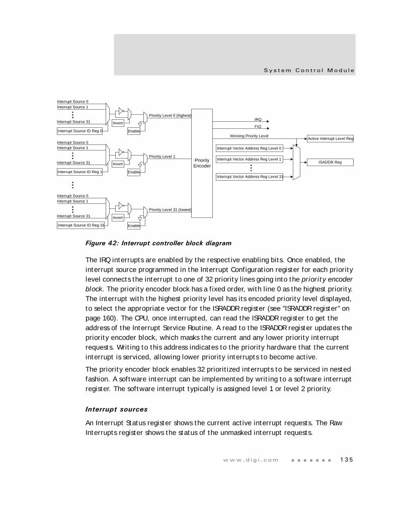
www.d i g i . com 135
Sys t em Con t r o l Modu l e
Figure 42: Interrupt controller block diagram
The IRQ interrupts are enabled by the respective enabling bits. Once enabled, the interrupt source programmed in the Interrupt Configuration register for each priority level connects the interrupt to one of 32 priority lines going into the priority encoder block. The priority encoder block has a fixed order, with line 0 as the highest priority. The interrupt with the highest priority level has its encoded priority level displayed, to select the appropriate vector for the ISRADDR register (see "ISRADDR register" on page 160). The CPU, once interrupted, can read the ISRADDR register to get the address of the Interrupt Service Routine. A read to the ISRADDR register updates the priority encoder block, which masks the current and any lower priority interrupt requests. Writing to this address indicates to the priority hardware that the current interrupt is serviced, allowing lower priority interrupts to become active.
The priority encoder block enables 32 prioritized interrupts to be serviced in nested fashion. A software interrupt can be implemented by writing to a software interrupt register. The software interrupt typically is assigned level 1 or level 2 priority.
Interrupt sources
An Interrupt Status register shows the current active interrupt requests. The Raw Interrupts register shows the status of the unmasked interrupt requests.
Interrupt Source 0Interrupt Source 1
Interrupt Source 31Priority Level 1
Interrupt Source ID Reg 1
Interrupt Source 0Interrupt Source 1
Interrupt Source 31Priority Level 0 (highest)
Interrupt Source ID Reg 0
Interrupt Source 0Interrupt Source 1
Interrupt Source 31Priority Level 31 (lowest)
Interrupt Source ID Reg 31
PriorityEncoder
IRQ
FIQ
Interrupt Vector Address Reg Level 1
Interrupt Vector Address Reg Level 31
Interrupt Vector Address Reg Level 0
Winning Priority Level
ISADDR Reg
Active Interrupt Level Reg
Enable
Invert
Enable
Invert
Enable
Invert
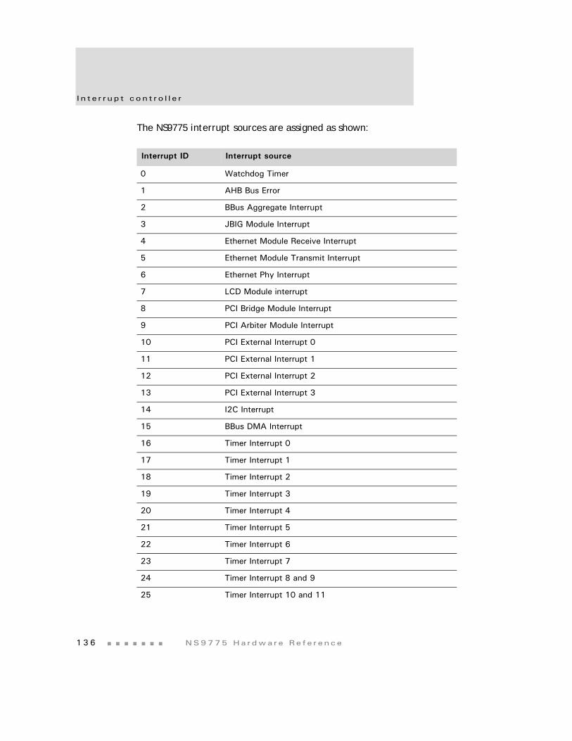
I n t e r r u p t c on t r o l l e r
1 3 6 NS9775 Ha r dwa r e Re f e r ence
The NS9775 interrupt sources are assigned as shown:
Interrupt ID Interrupt source
0 Watchdog Timer
1 AHB Bus Error
2 BBus Aggregate Interrupt
3 JBIG Module Interrupt
4 Ethernet Module Receive Interrupt
5 Ethernet Module Transmit Interrupt
6 Ethernet Phy Interrupt
7 LCD Module interrupt
8 PCI Bridge Module Interrupt
9 PCI Arbiter Module Interrupt
10 PCI External Interrupt 0
11 PCI External Interrupt 1
12 PCI External Interrupt 2
13 PCI External Interrupt 3
14 I2C Interrupt
15 BBus DMA Interrupt
16 Timer Interrupt 0
17 Timer Interrupt 1
18 Timer Interrupt 2
19 Timer Interrupt 3
20 Timer Interrupt 4
21 Timer Interrupt 5
22 Timer Interrupt 6
23 Timer Interrupt 7
24 Timer Interrupt 8 and 9
25 Timer Interrupt 10 and 11
www.d i g i . com 137
Sys t em Con t r o l Modu l e
Vectored interrupt controller (VIC) flow
A vectored interrupt controller allows a reasonable interrupt latency for IRQ-line interrupts. When an interrupt occurs, the CPU processor determines whether the interrupt is from a FIQ or IRQ line. If the interrupt comes from the FIQ vector, the interrupt service routine can be executed without knowing the interrupt source.
If the interrupt comes from the IRQ vector, the CPU performs these steps:
1 Reads the service routine address from the VIC’s ISRADDR register. The read updates the VIC’s priority hardware to prevent current or any lower priority interrupts from interrupting until the higher priority interrupt has occurred.
2 Branches to the interrupt service routine and stacks the workspace so the IRQ can be enabled.
3 Executes the interrupt service routine.
4 Clears the current interrupt from the source.
5 Disables the IRQ and restores the workplace.
6 Writes to the ISRADDR register to clear the current interrupt path in the VIC’s priority hardware. Any value can be written.
7 Returns from the interrupt service routine.
System attributes
System software can configure these NS9775 system attributes:
Little endian/big endian mode
26 Timer Interrupt 12 and 13
27 Timer Interrupt 14 and 15
28 External Interrupt 0
29 External Interrupt 1
30 External Interrupt 2
31 External Interrupt 3
Interrupt ID Interrupt source
Sys t em a t t r i b u t e s
1 3 8 NS9775 Ha r dwa r e Re f e r ence
Watchdog timer enable
Watchdog timeout generates IRQ/FIQ/RESET
Watchdog timeout interval
Enable/disable ERROR response for misaligned data access
System module clock enables
Enable access to internal registers in USER mode
Bus monitor enable
Bus monitor timeout interval
Bus arbiter timer enable
Bus arbiter timeout period
Bus arbiter timeout response (IRQ/FIQ/RESET)
Bus bandwidth configuration
Wake-up processor enable
PLL configuration
PLL operating parameters are initialized on a powerup hardware reset. Software reads the powerup hardware settings by reading the status fields in the PLL Configuration register (see "PLL Configuration register" on page 171). Software can change the PLL configuration after a powerup reset by writing to the appropriate SW field in the PLL Configuration register (see "PLL Configuration register," beginning on page 171). Once the new settings have been written, the PLL SW change bit must be set (see page 172). The PLL settings then are written to the PLL, and the system is reset.
The PLL can be configured at powerup by placing pulldowns on the external memory address pins. NS9775 provides internal pullups to produce a default configuration; see "Bootstrap initialization" on page 139 for information about the powerup configuration.
Figure 43 shows how the PLL clock is used to provide the NS9775 system clocks.
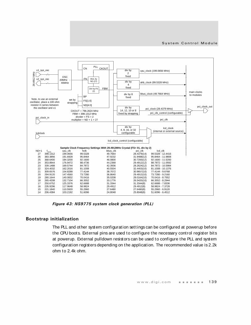
www.d i g i . com 139
Sys t em Con t r o l Modu l e
Figure 43: NS9775 system clock generation (PLL)
Bootstrap initialization
The PLL and other system configuration settings can be configured at powerup before the CPU boots. External pins are used to configure the necessary control register bits at powerup. External pulldown resistors can be used to configure the PLL and system configuration registers depending on the application. The recommended value is 2.2k ohm to 2.4k ohm.
PLL
FN
FBM
FS[1:0]
ND[4:0]
CKOUT = 796.2624 MHzFBM = 398.1312 MHz
divider = FS = 2multiplier = ND + 1 = 27
CN
set bystrapping
OSC20MHz -
40MHz
BPNote, to use an external
oscillator, place a 100 ohmresistor in series between
the oscillator and x1
29.4
912
MH
z
x1_sys_osc
x2_sys_osc
div by2
fixed
div by4
fixed
div by 8fixed
cpu_clock (199.0656 MHz)
ahb_clock (99.5328 MHz)
bbus_clock (49.7664 MHz)
div by14, 12, 10 or 8
fixed by strapping
div by4, 8, 16, or 32configurable
lcd_clock(internal or external source)
lcd_clock_control (configurable)
pci_clk_control (configurable)
pci_clock_out
main clocksto modules
pci_clock (28.4379 MHz)
lcdclock
pci_clock_inpci_clk
CKOUT
MUL byND (27)
DIV by FS(2)
Sample Clock Frequency Settings With 29.4912MHz Crystal (FS= 01, div by 2)ND+1 fVCO cpu_clk hclk bbus_clk pci_clk lcd_clk 27 398.1312 199.0656 99.5328 49.7664 28.4379(14) 99.5328 - 12.4416 26 383.3856 191.6928 95.8464 47.9232 31.9488(12) 95.8464 - 11.9808 25 368.6400 184.3200 92.1600 46.0800 30.7200(12) 92.1600 - 11.5200 24 353.8944 176.9472 88.4736 44.2368 29.4912(12) 88.7872 - 11.0592 23 339.1488 169.5744 84.7872 42.3936 28.2624(12) 84.7872 - 10.5984 22 324.4032 162.2016 81.1008 40.5504 32.4403(10) 81.1008 - 10.1376 21 309.6576 154.8288 77.4144 38.7072 30.9657(10) 77.4144 - 9.6768 20 294.9120 147.4560 73.7280 36.8640 29.4912(10) 73.7280 - 9.2160 19 280.1644 140.0832 70.0416 35.0208 28.0164(10) 70.0416 - 8.7552 18 265.4208 132.7104 66.3552 33.1776 26.5420(10) 66.3552 - 8.2944 17 250.6752 125.3376 62.6688 31.3344 31.3344(8) 62.6688 - 7.8336 16 235.9296 117.9648 58.9824 29.4912 29.4912(8) 58.9824 - 7.3728 15 221.1840 110.5920 55.2960 27.6480 27.6480(8) 55.2960 - 6.9120 14 206.4384 103.2192 51.6096 24.8048 25.8048(8) 51.6096 - 6.4512
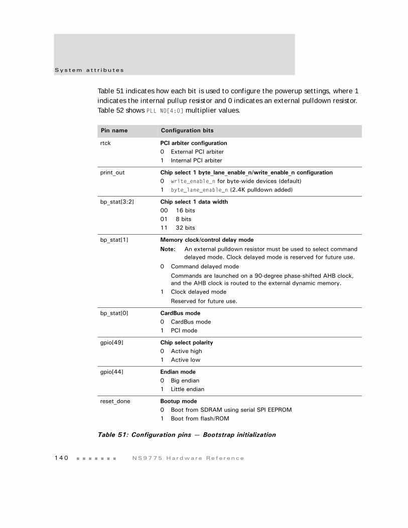
Sys t em a t t r i b u t e s
1 4 0 NS9775 Ha r dwa r e Re f e r ence
Table 51 indicates how each bit is used to configure the powerup settings, where 1 indicates the internal pullup resistor and 0 indicates an external pulldown resistor. Table 52 shows PLL ND[4:0] multiplier values.
Pin name Configuration bits
rtck PCI arbiter configuration0 External PCI arbiter1 Internal PCI arbiter
print_out Chip select 1 byte_lane_enable_n/write_enable_n configuration 0 write_enable_n for byte-wide devices (default)1 byte_lane_enable_n (2.4K pulldown added)
bp_stat[3:2] Chip select 1 data width 00 16 bits01 8 bits11 32 bits
bp_stat[1] Memory clock/control delay mode
Note: An external pulldown resistor must be used to select command delayed mode. Clock delayed mode is reserved for future use.
0 Command delayed mode
Commands are launched on a 90-degree phase-shifted AHB clock, and the AHB clock is routed to the external dynamic memory.
1 Clock delayed mode
Reserved for future use.
bp_stat[0] CardBus mode 0 CardBus mode1 PCI mode
gpio[49] Chip select polarity0 Active high1 Active low
gpio[44] Endian mode0 Big endian1 Little endian
reset_done Bootup mode0 Boot from SDRAM using serial SPI EEPROM1 Boot from flash/ROM
Table 51: Configuration pins — Bootstrap initialization
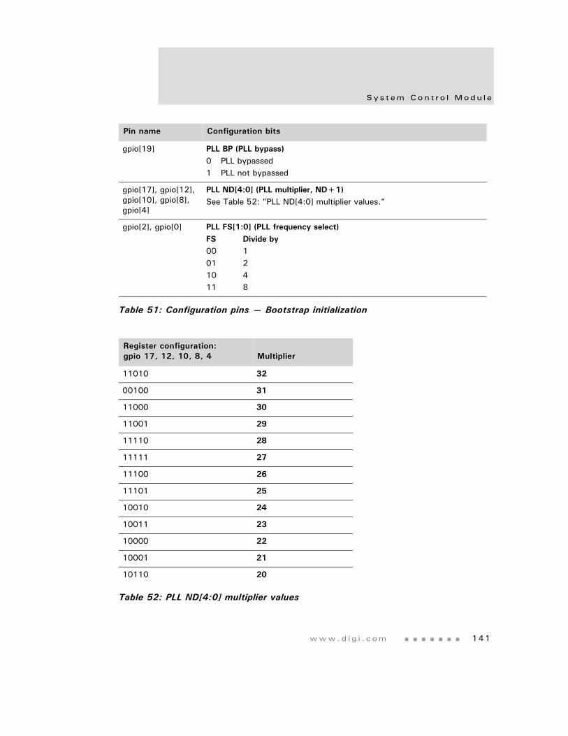
www.d i g i . com 141
Sys t em Con t r o l Modu l e
gpio[19] PLL BP (PLL bypass)0 PLL bypassed1 PLL not bypassed
gpio[17], gpio[12], gpio[10], gpio[8], gpio[4]
PLL ND[4:0] (PLL multiplier, ND+1)See Table 52: "PLL ND[4:0] multiplier values."
gpio[2], gpio[0] PLL FS[1:0] (PLL frequency select)FS Divide by00 101 210 411 8
Register configuration:gpio 17, 12, 10, 8, 4 Multiplier
11010 32
00100 31
11000 30
11001 29
11110 28
11111 27
11100 26
11101 25
10010 24
10011 23
10000 22
10001 21
10110 20
Table 52: PLL ND[4:0] multiplier values
Pin name Configuration bits
Table 51: Configuration pins — Bootstrap initialization
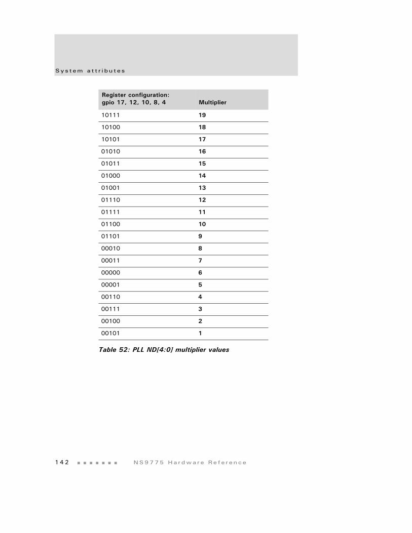
Sys t em a t t r i b u t e s
1 4 2 NS9775 Ha r dwa r e Re f e r ence
10111 19
10100 18
10101 17
01010 16
01011 15
01000 14
01001 13
01110 12
01111 11
01100 10
01101 9
00010 8
00011 7
00000 6
00001 5
00110 4
00111 3
00100 2
00101 1
Register configuration:gpio 17, 12, 10, 8, 4 Multiplier
Table 52: PLL ND[4:0] multiplier values
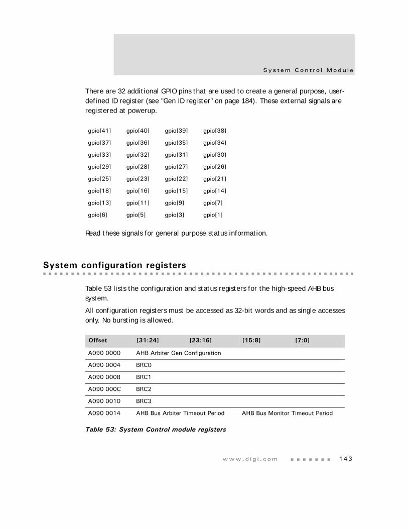
www.d i g i . com 143
Sys t em Con t r o l Modu l e
There are 32 additional GPIO pins that are used to create a general purpose, user-defined ID register (see "Gen ID register" on page 184). These external signals are registered at powerup.
Read these signals for general purpose status information.
System configuration registers
Table 53 lists the configuration and status registers for the high-speed AHB bus system.
All configuration registers must be accessed as 32-bit words and as single accesses only. No bursting is allowed.
gpio[41] gpio[40] gpio[39] gpio[38]
gpio[37] gpio[36] gpio[35] gpio[34]
gpio[33] gpio[32] gpio[31] gpio[30]
gpio[29] gpio[28] gpio[27] gpio[26]
gpio[25] gpio[23] gpio[22] gpio[21]
gpio[18] gpio[16] gpio[15] gpio[14]
gpio[13] gpio[11] gpio[9] gpio[7]
gpio[6] gpio[5] gpio[3] gpio[1]
Offset [31:24] [23:16] [15:8] [7:0]
A090 0000 AHB Arbiter Gen Configuration
A090 0004 BRC0
A090 0008 BRC1
A090 000C BRC2
A090 0010 BRC3
A090 0014 AHB Bus Arbiter Timeout Period AHB Bus Monitor Timeout Period
Table 53: System Control module registers
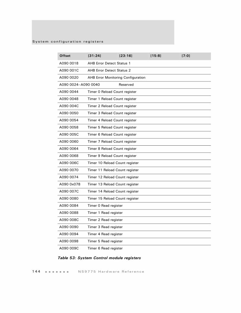
Sys t em con f i g u r a t i o n r e g i s t e r s
1 4 4 NS9775 Ha r dwa r e Re f e r ence
A090 0018 AHB Error Detect Status 1
A090 001C AHB Error Detect Status 2
A090 0020 AHB Error Monitoring Configuration
A090 0024–A090 0040 Reserved
A090 0044 Timer 0 Reload Count register
A090 0048 Timer 1 Reload Count register
A090 004C Timer 2 Reload Count register
A090 0050 Timer 3 Reload Count register
A090 0054 Timer 4 Reload Count register
A090 0058 Timer 5 Reload Count register
A090 005C Timer 6 Reload Count register
A090 0060 Timer 7 Reload Count register
A090 0064 Timer 8 Reload Count register
A090 0068 Timer 9 Reload Count register
A090 006C Timer 10 Reload Count register
A090 0070 Timer 11 Reload Count register
A090 0074 Timer 12 Reload Count register
A090 0x078 Timer 13 Reload Count register
A090 007C Timer 14 Reload Count register
A090 0080 Timer 15 Reload Count register
A090 0084 Timer 0 Read register
A090 0088 Timer 1 Read register
A090 008C Timer 2 Read register
A090 0090 Timer 3 Read register
A090 0094 Timer 4 Read register
A090 0098 Timer 5 Read register
A090 009C Timer 6 Read register
Offset [31:24] [23:16] [15:8] [7:0]
Table 53: System Control module registers
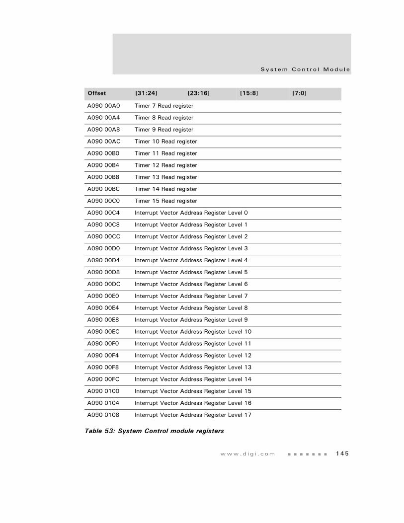
www.d i g i . com 145
Sys t em Con t r o l Modu l e
A090 00A0 Timer 7 Read register
A090 00A4 Timer 8 Read register
A090 00A8 Timer 9 Read register
A090 00AC Timer 10 Read register
A090 00B0 Timer 11 Read register
A090 00B4 Timer 12 Read register
A090 00B8 Timer 13 Read register
A090 00BC Timer 14 Read register
A090 00C0 Timer 15 Read register
A090 00C4 Interrupt Vector Address Register Level 0
A090 00C8 Interrupt Vector Address Register Level 1
A090 00CC Interrupt Vector Address Register Level 2
A090 00D0 Interrupt Vector Address Register Level 3
A090 00D4 Interrupt Vector Address Register Level 4
A090 00D8 Interrupt Vector Address Register Level 5
A090 00DC Interrupt Vector Address Register Level 6
A090 00E0 Interrupt Vector Address Register Level 7
A090 00E4 Interrupt Vector Address Register Level 8
A090 00E8 Interrupt Vector Address Register Level 9
A090 00EC Interrupt Vector Address Register Level 10
A090 00F0 Interrupt Vector Address Register Level 11
A090 00F4 Interrupt Vector Address Register Level 12
A090 00F8 Interrupt Vector Address Register Level 13
A090 00FC Interrupt Vector Address Register Level 14
A090 0100 Interrupt Vector Address Register Level 15
A090 0104 Interrupt Vector Address Register Level 16
A090 0108 Interrupt Vector Address Register Level 17
Offset [31:24] [23:16] [15:8] [7:0]
Table 53: System Control module registers
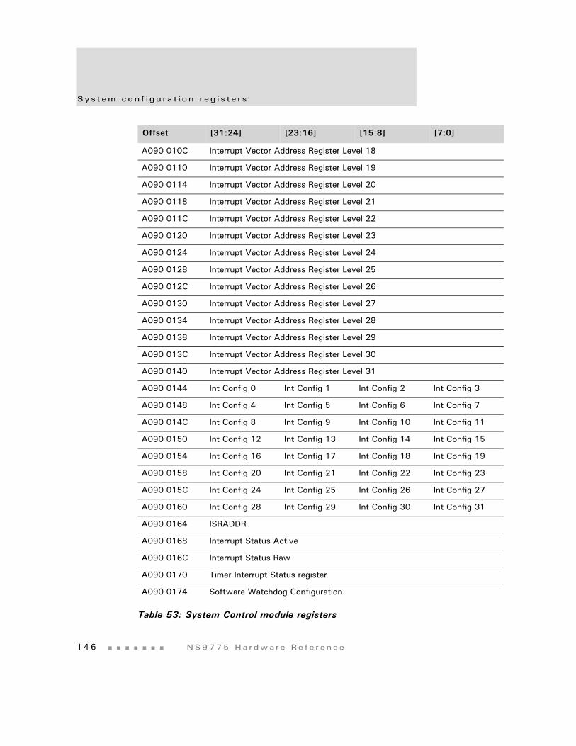
Sys t em con f i g u r a t i o n r e g i s t e r s
1 4 6 NS9775 Ha r dwa r e Re f e r ence
A090 010C Interrupt Vector Address Register Level 18
A090 0110 Interrupt Vector Address Register Level 19
A090 0114 Interrupt Vector Address Register Level 20
A090 0118 Interrupt Vector Address Register Level 21
A090 011C Interrupt Vector Address Register Level 22
A090 0120 Interrupt Vector Address Register Level 23
A090 0124 Interrupt Vector Address Register Level 24
A090 0128 Interrupt Vector Address Register Level 25
A090 012C Interrupt Vector Address Register Level 26
A090 0130 Interrupt Vector Address Register Level 27
A090 0134 Interrupt Vector Address Register Level 28
A090 0138 Interrupt Vector Address Register Level 29
A090 013C Interrupt Vector Address Register Level 30
A090 0140 Interrupt Vector Address Register Level 31
A090 0144 Int Config 0 Int Config 1 Int Config 2 Int Config 3
A090 0148 Int Config 4 Int Config 5 Int Config 6 Int Config 7
A090 014C Int Config 8 Int Config 9 Int Config 10 Int Config 11
A090 0150 Int Config 12 Int Config 13 Int Config 14 Int Config 15
A090 0154 Int Config 16 Int Config 17 Int Config 18 Int Config 19
A090 0158 Int Config 20 Int Config 21 Int Config 22 Int Config 23
A090 015C Int Config 24 Int Config 25 Int Config 26 Int Config 27
A090 0160 Int Config 28 Int Config 29 Int Config 30 Int Config 31
A090 0164 ISRADDR
A090 0168 Interrupt Status Active
A090 016C Interrupt Status Raw
A090 0170 Timer Interrupt Status register
A090 0174 Software Watchdog Configuration
Offset [31:24] [23:16] [15:8] [7:0]
Table 53: System Control module registers
www.d i g i . com 147
Sys t em Con t r o l Modu l e
A090 0178 Software Watchdog Timer
A090 017C Clock Configuration register
A090 0180 Reset and Sleep Control register
A090 0184 Miscellaneous System Configuration register
A090 0188 PLL Configuration register
A090 018C Active Interrupt Level register
A090 0190 Timer 0 Control register
A090 0194 Timer 1 Control register
A090 0198 Timer 2 Control register
A090 019C Timer 3 Control register
A090 01A0 Timer 4 Control register
A090 01A4 Timer 5 Control register
A090 01A8 Timer 6 Control register
A090 01AC Timer 7 Control register
A090 01B0 Timer 8 Control register
A090 01B4 Timer 9 Control register
A090 01B8 Timer 10 Control register
A090 01BC Timer 11 Control register
A090 01C0 Timer 12 Control register
A090 01C4 Timer 13 Control register
A090 01C8 Timer 14 Control register
A090 01CC Timer 15 Control register
A090 01D0 System Memory Chip Select 0 Dynamic Memory Base
A090 01D4 System Memory Chip Select 0 Dynamic Memory Mask
A090 01D8 System Memory Chip Select 1 Dynamic Memory Base
A090 01DC System Memory Chip Select 1 Dynamic Memory Mask
A090 01E0 System Memory Chip Select 2 Dynamic Memory Base
Offset [31:24] [23:16] [15:8] [7:0]
Table 53: System Control module registers
Sys t em con f i g u r a t i o n r e g i s t e r s
1 4 8 NS9775 Ha r dwa r e Re f e r ence
A090 01E4 System Memory Chip Select 2 Dynamic Memory Mask
A090 01E8 System Memory Chip Select 3 Dynamic Memory Base
A090 01EC System Memory Chip Select 3 Dynamic Memory Mask
A090 01F0 System Memory Chip Select 0 Static Memory Base
A090 01F4 System Memory Chip Select 0 Static Memory Mask
A090 01F8 System Memory Chip Select 1 Static Memory Base
A090 01FC System Memory Chip Select 1 Static Memory Mask
A090 0200 System Memory Chip Select 2 Static Memory Base
A090 0204 System Memory Chip Select 2 Static Memory Mask
A090 0208 System Memory Chip Select 3 Static Memory Base
A090 020C System Memory Chip Select 3 Static Memory Mask
A090 0210 GenID— General purpose, user-defined ID register
A090 0214 External Interrupt 0 Control register
A090 0218 External Interrupt 1 Control register
A090 021C External Interrupt 2 Control register
A090 0220 External Interrupt 3 Control register
Offset [31:24] [23:16] [15:8] [7:0]
Table 53: System Control module registers
www.d i g i . com 149
Sys t em Con t r o l Modu l e
AHB Arbiter Gen Configuration register
Address: A090 0000The AHB Arbiter Gen Configuration register contains miscellaneous control settings for the AHB bus arbiter.
Register bit assignment
Bits Access Mnemonic Reset Description
D31:01 N/A Reserved N/A N/A
D00 R/W EXMA 0x0 CPU external memory access mode0 Enable direct access to external memory
through Slv11 Disable direct access to external memory,
arbitrate with other masters through Slv0
Table 54: AHB Arbiter Gen Configuration register
EXMA
13 12 11 10 9 8 7 6 5 4 3 2 1 015 14
31 29 28 27 26 25 24 23 22 21 20 19 18 17 1630
Reserved
Reserved
Sys t em con f i g u r a t i o n r e g i s t e r s
1 5 0 NS9775 Ha r dwa r e Re f e r ence
BRC0, BRC1, BRC2, and BRC3 registers
Address: A090 0004 / 0008 / 000C / 0010The BRC[0:3] registers control the AHB arbiter bandwidth allocation scheme. Table 55 shows how the channels are assigned in the four registers. Table 56 shows the bit definition, or format, for each channel, using data bits [07:00] as the example.
Register bit assignment
Register name [31:24] [23:16] [15:08] [07:00]
BRC0 Channel 0 Channel 1 Channel 2 Channel 3
BRC1 Channel 4 Channel 5 Channel 6 Channel 7
BRC2 Channel 8 Channel 9 Channel 10 Channel 11
BRC3 Channel 12 Channel 13 Channel 14 Channel 15
Table 55: BRC channel assignment
Bits Access Mnemonic Reset Description
D07 R/W CEB 0x0 Channel enable bit0 Disable1 Enable
D06 N/A Reserved N/A N/A
Table 56: BRC0, BRC1, BRC2, BRC3 register
HMSTR
13 12 11 10 9 8 7 6 5 4 3 2 1 015 14
31 29 28 27 26 25 24 23 22 21 20 19 18 17 1630
Channel 0, 4, 8, or 12 Channel 1, 5, 9, or 13
Channel 2, 6, 10, or 14Channel 3, 7, 11, or 15
CEB Rsvd BRF
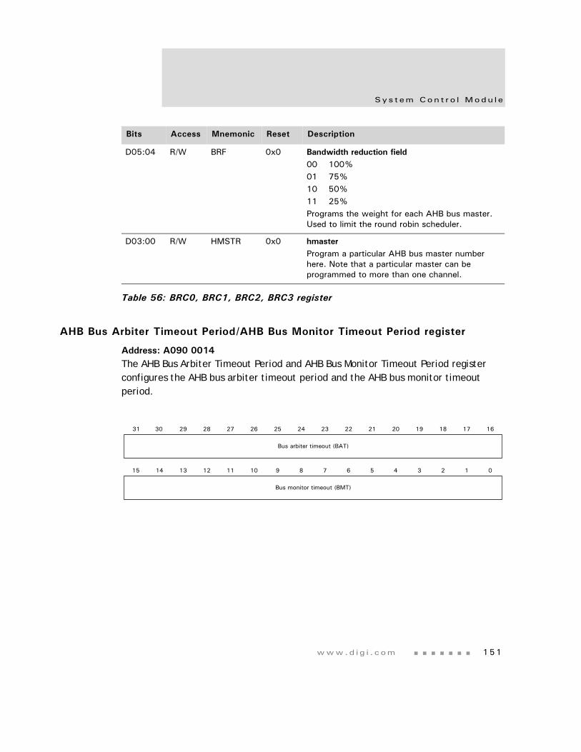
www.d i g i . com 151
Sys t em Con t r o l Modu l e
AHB Bus Arbiter Timeout Period/AHB Bus Monitor Timeout Period register
Address: A090 0014The AHB Bus Arbiter Timeout Period and AHB Bus Monitor Timeout Period register configures the AHB bus arbiter timeout period and the AHB bus monitor timeout period.
D05:04 R/W BRF 0x0 Bandwidth reduction field00 100%01 75%10 50%11 25%Programs the weight for each AHB bus master. Used to limit the round robin scheduler.
D03:00 R/W HMSTR 0x0 hmasterProgram a particular AHB bus master number here. Note that a particular master can be programmed to more than one channel.
Bits Access Mnemonic Reset Description
Table 56: BRC0, BRC1, BRC2, BRC3 register
13 12 11 10 9 8 7 6 5 4 3 2 1 015 14
31 29 28 27 26 25 24 23 22 21 20 19 18 17 1630
Bus arbiter timeout (BAT)
Bus monitor timeout (BMT)
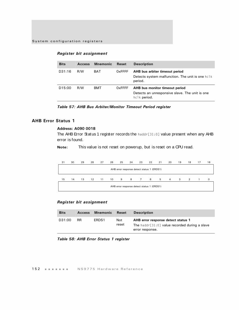
Sys t em con f i g u r a t i o n r e g i s t e r s
1 5 2 NS9775 Ha r dwa r e Re f e r ence
Register bit assignment
AHB Error Status 1
Address: A090 0018The AHB Error Status 1 register records the haddr[31:0] value present when any AHB error is found.
Note: This value is not reset on powerup, but is reset on a CPU read.
Register bit assignment
Bits Access Mnemonic Reset Description
D31:16 R/W BAT 0xFFFF AHB bus arbiter timeout periodDetects system malfunction. The unit is one hclk period.
D15:00 R/W BMT 0xFFFF AHB bus monitor timeout periodDetects an unresponsive slave. The unit is one hclk period.
Table 57: AHB Bus Arbiter/Monitor Timeout Period register
Bits Access Mnemonic Reset Description
D31:00 RR ERDS1 Not reset
AHB error response detect status 1The haddr[31:0] value recorded during a slave error response.
Table 58: AHB Error Status 1 register
13 12 11 10 9 8 7 6 5 4 3 2 1 015 14
31 29 28 27 26 25 24 23 22 21 20 19 18 17 1630
AHB error response detect status 1 (ERDS1)
AHB error response detect status 1 (ERDS1)
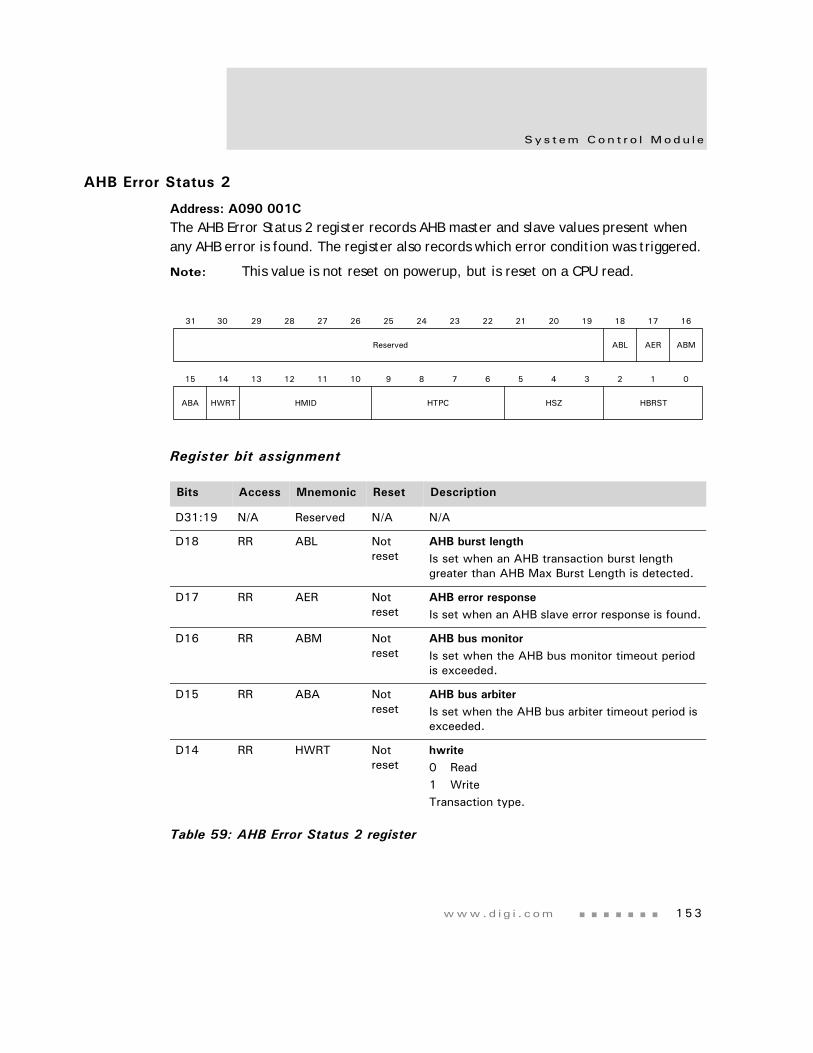
www.d i g i . com 153
Sys t em Con t r o l Modu l e
AHB Error Status 2
Address: A090 001CThe AHB Error Status 2 register records AHB master and slave values present when any AHB error is found. The register also records which error condition was triggered.
Note: This value is not reset on powerup, but is reset on a CPU read.
Register bit assignment
Bits Access Mnemonic Reset Description
D31:19 N/A Reserved N/A N/A
D18 RR ABL Not reset
AHB burst lengthIs set when an AHB transaction burst length greater than AHB Max Burst Length is detected.
D17 RR AER Not reset
AHB error responseIs set when an AHB slave error response is found.
D16 RR ABM Not reset
AHB bus monitorIs set when the AHB bus monitor timeout period is exceeded.
D15 RR ABA Not reset
AHB bus arbiterIs set when the AHB bus arbiter timeout period is exceeded.
D14 RR HWRT Not reset
hwrite0 Read1 WriteTransaction type.
Table 59: AHB Error Status 2 register
ABL
13 12 11 10 9 8 7 6 5 4 3 2 1 015 14
31 29 28 27 26 25 24 23 22 21 20 19 18 17 1630
Reserved AER ABM
ABA HWRT HMID HTPC HSZ HBRST
Sys t em con f i g u r a t i o n r e g i s t e r s
1 5 4 NS9775 Ha r dwa r e Re f e r ence
D13:10 RR HMID Not reset
hmaster [3:0]Initiating master identifier. SeeTable 50 on page 129.
D09:06 RR HTPC Not reset
hprot[3:0]Transaction protection code:hprot[3]0 Not cacheable1 Cacheablehprot[2]0 Not bufferable1 Bufferablehprot[1]0 User access1 Privileged accesshprot[0]0 Opcode fetch1 Data access
D05:03 RR HSZ Not reset
hsize[2:0]Transaction size:000 8 bits001 16 bits010 32 bits
D02:00 RR HBRST Not reset
hburst[2:0]Transaction burst type:000 Single transfer001 Incrementing transfer of unspecified length010 4-beat wrapping burst011 4-beat incrementing burst100 8-beat wrapping burst101 8-beat incrementing burst110 16-beat wrapping burst111 16-beat incrementing burst
Bits Access Mnemonic Reset Description
Table 59: AHB Error Status 2 register
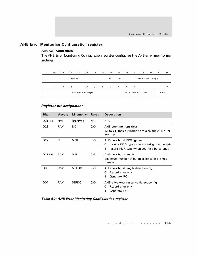
www.d i g i . com 155
Sys t em Con t r o l Modu l e
AHB Error Monitoring Configuration register
Address: A090 0020The AHB Error Monitoring Configuration register configures the AHB error monitoring settings.
Register bit assignment
Bits Access Mnemonic Reset Description
D31:24 N/A Reserved N/A N/A
D23 R/W EIC 0x0 AHB error interrupt clearWrite a 1, then a 0 in this bit to clear the AHB error interrupt.
D22 R MBII 0x0 AHB max burst INCR ignore0 Include INCR type when counting burst length1 Ignore INCR type when counting burst length
D21:06 R/W MBL 0x8 AHB max burst lengthMaximum number of bursts allowed in a single transfer.
D05 R/W MBLDC 0x0 AHB max burst length detect config0 Record error only1 Generate IRQ
D04 R/W SERDC 0x0 AHB slave error response detect config0 Record error only1 Generate IRQ
Table 60: AHB Error Monitoring Configuration register
MBLDC
13 12 11 10 9 8 7 6 5 4 3 2 1 015 14
31 29 28 27 26 25 24 23 22 21 20 19 18 17 1630
Reserved EIC MBII AHB max burst length
AHB max burst length SERDC BMTC BATC
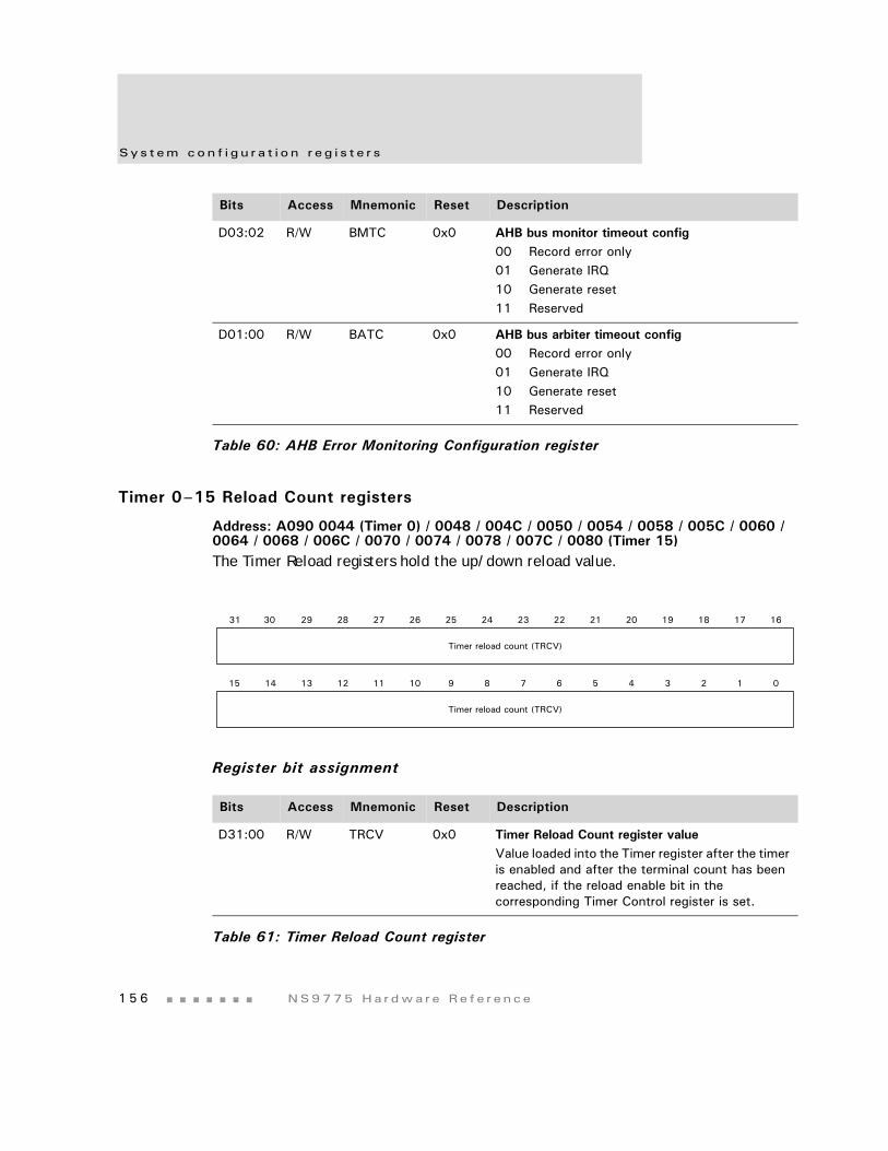
Sys t em con f i g u r a t i o n r e g i s t e r s
1 5 6 NS9775 Ha r dwa r e Re f e r ence
Timer 0–15 Reload Count registers
Address: A090 0044 (Timer 0) / 0048 / 004C / 0050 / 0054 / 0058 / 005C / 0060 / 0064 / 0068 / 006C / 0070 / 0074 / 0078 / 007C / 0080 (Timer 15)The Timer Reload registers hold the up/down reload value.
Register bit assignment
D03:02 R/W BMTC 0x0 AHB bus monitor timeout config00 Record error only01 Generate IRQ10 Generate reset11 Reserved
D01:00 R/W BATC 0x0 AHB bus arbiter timeout config00 Record error only01 Generate IRQ10 Generate reset11 Reserved
Bits Access Mnemonic Reset Description
Table 60: AHB Error Monitoring Configuration register
Bits Access Mnemonic Reset Description
D31:00 R/W TRCV 0x0 Timer Reload Count register valueValue loaded into the Timer register after the timer is enabled and after the terminal count has been reached, if the reload enable bit in the corresponding Timer Control register is set.
Table 61: Timer Reload Count register
13 12 11 10 9 8 7 6 5 4 3 2 1 015 14
31 29 28 27 26 25 24 23 22 21 20 19 18 17 1630
Timer reload count (TRCV)
Timer reload count (TRCV)
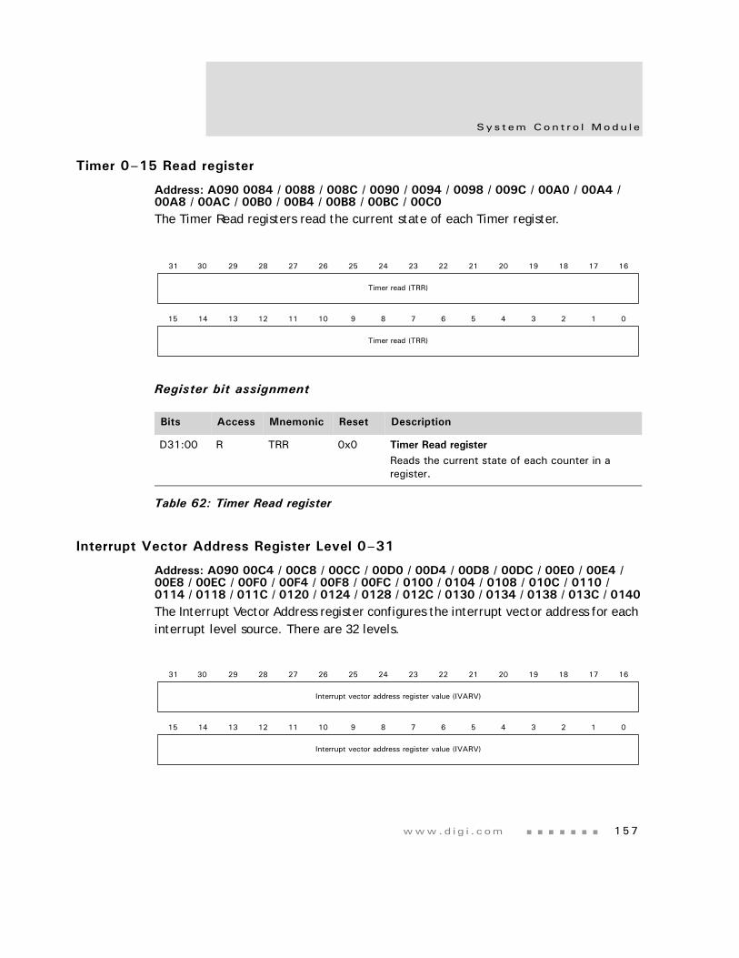
www.d i g i . com 157
Sys t em Con t r o l Modu l e
Timer 0–15 Read register
Address: A090 0084 / 0088 / 008C / 0090 / 0094 / 0098 / 009C / 00A0 / 00A4 / 00A8 / 00AC / 00B0 / 00B4 / 00B8 / 00BC / 00C0 The Timer Read registers read the current state of each Timer register.
Register bit assignment
Interrupt Vector Address Register Level 0–31
Address: A090 00C4 / 00C8 / 00CC / 00D0 / 00D4 / 00D8 / 00DC / 00E0 / 00E4 / 00E8 / 00EC / 00F0 / 00F4 / 00F8 / 00FC / 0100 / 0104 / 0108 / 010C / 0110 / 0114 / 0118 / 011C / 0120 / 0124 / 0128 / 012C / 0130 / 0134 / 0138 / 013C / 0140The Interrupt Vector Address register configures the interrupt vector address for each interrupt level source. There are 32 levels.
Bits Access Mnemonic Reset Description
D31:00 R TRR 0x0 Timer Read registerReads the current state of each counter in a register.
Table 62: Timer Read register
13 12 11 10 9 8 7 6 5 4 3 2 1 015 14
31 29 28 27 26 25 24 23 22 21 20 19 18 17 1630
Timer read (TRR)
Timer read (TRR)
13 12 11 10 9 8 7 6 5 4 3 2 1 015 14
31 29 28 27 26 25 24 23 22 21 20 19 18 17 1630
Interrupt vector address register value (IVARV)
Interrupt vector address register value (IVARV)
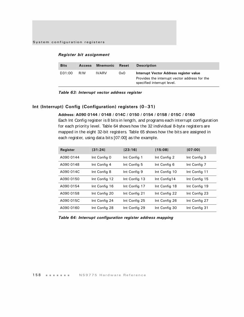
Sys t em con f i g u r a t i o n r e g i s t e r s
1 5 8 NS9775 Ha r dwa r e Re f e r ence
Register bit assignment
Int (Interrupt) Config (Configuration) registers (0–31)
Address: A090 0144 / 0148 / 014C / 0150 / 0154 / 0158 / 015C / 0160Each Int Config register is 8 bits in length, and programs each interrupt configuration for each priority level. Table 64 shows how the 32 individual 8-byte registers are mapped in the eight 32-bit registers. Table 65 shows how the bits are assigned in each register, using data bits [07:00] as the example.
Bits Access Mnemonic Reset Description
D31:00 R/W IVARV 0x0 Interrupt Vector Address register valueProvides the interrupt vector address for the specified interrupt level.
Table 63: Interrupt vector address register
Register [31:24] [23:16] [15:08] [07:00]
A090 0144 Int Config 0 Int Config 1 Int Config 2 Int Config 3
A090 0148 Int Config 4 Int Config 5 Int Config 6 Int Config 7
A090 014C Int Config 8 Int Config 9 Int Config 10 Int Config 11
A090 0150 Int Config 12 Int Config 13 Int Config14 Int Config 15
A090 0154 Int Config 16 Int Config 17 Int Config 18 Int Config 19
A090 0158 Int Config 20 Int Config 21 Int Config 22 Int Config 23
A090 015C Int Config 24 Int Config 25 Int Config 26 Int Config 27
A090 0160 Int Config 28 Int Config 29 Int Config 30 Int Config 31
Table 64: Interrupt configuration register address mapping
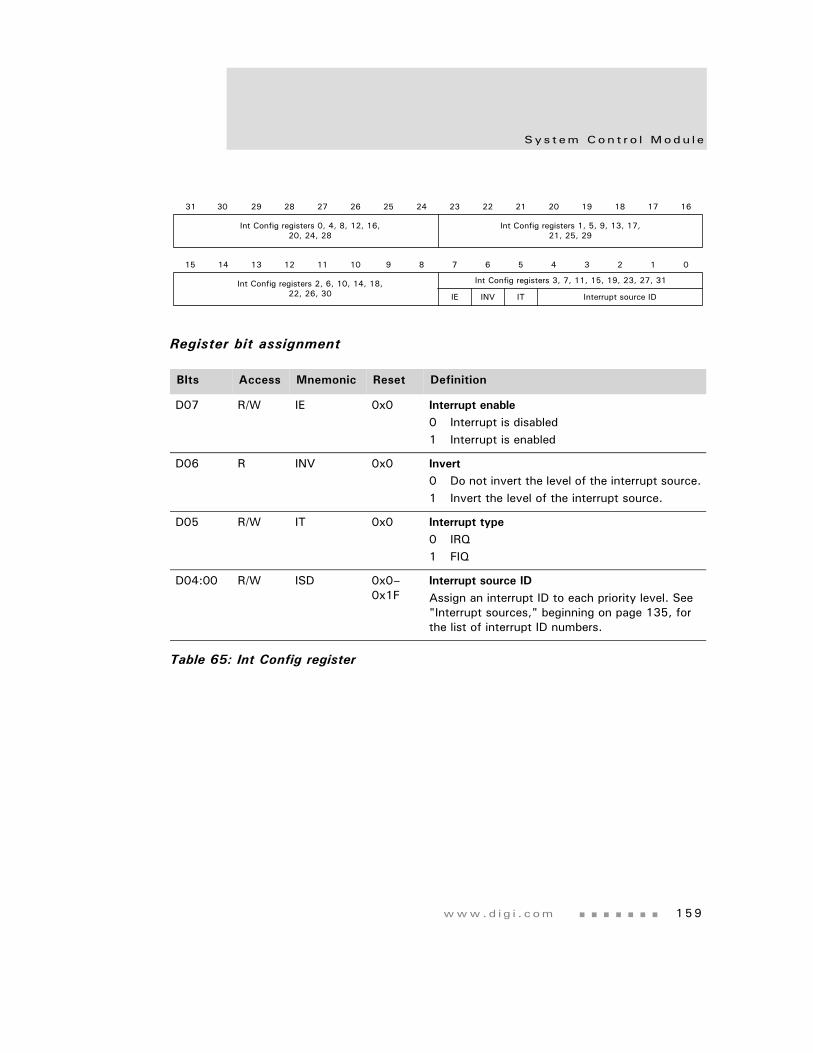
www.d i g i . com 159
Sys t em Con t r o l Modu l e
Register bit assignment
BIts Access Mnemonic Reset Definition
D07 R/W IE 0x0 Interrupt enable0 Interrupt is disabled1 Interrupt is enabled
D06 R INV 0x0 Invert0 Do not invert the level of the interrupt source.1 Invert the level of the interrupt source.
D05 R/W IT 0x0 Interrupt type0 IRQ1 FIQ
D04:00 R/W ISD 0x0–0x1F
Interrupt source IDAssign an interrupt ID to each priority level. See "Interrupt sources," beginning on page 135, for the list of interrupt ID numbers.
Table 65: Int Config register
Interrupt source ID
13 12 11 10 9 8 7 6 5 4 3 2 1 015 14
31 29 28 27 26 25 24 23 22 21 20 19 18 17 1630
IE INV IT
Int Config registers 0, 4, 8, 12, 16,20, 24, 28
Int Config registers 1, 5, 9, 13, 17,21, 25, 29
Int Config registers 2, 6, 10, 14, 18,22, 26, 30
Int Config registers 3, 7, 11, 15, 19, 23, 27, 31
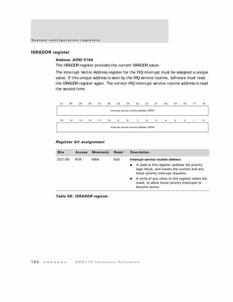
Sys t em con f i g u r a t i o n r e g i s t e r s
1 6 0 NS9775 Ha r dwa r e Re f e r ence
ISRADDR register
Address: A090 0164The ISRADDR register provides the current ISRADDR value.
The Interrupt Vector Address register for the FIQ interrupt must be assigned a unique value. If this unique address is seen by the IRQ service routine, software must read the ISRADDR register again. The correct IRQ interrupt service routine address is read the second time.
Register bit assignment
Bits Access Mnemonic Reset Description
D31:00 R/W ISRA 0x0 Interrupt service routine address
A read to this register updates the priority logic block, and masks the current and any lower priority interrupt requests.
A write of any value to this register clears the mask, to allow lower priority interrupts to become active.
Table 66: ISRADDR register
13 12 11 10 9 8 7 6 5 4 3 2 1 015 14
31 29 28 27 26 25 24 23 22 21 20 19 18 17 1630
Interrupt service routine address (ISRA)
Interrupt service routine address (ISRA)
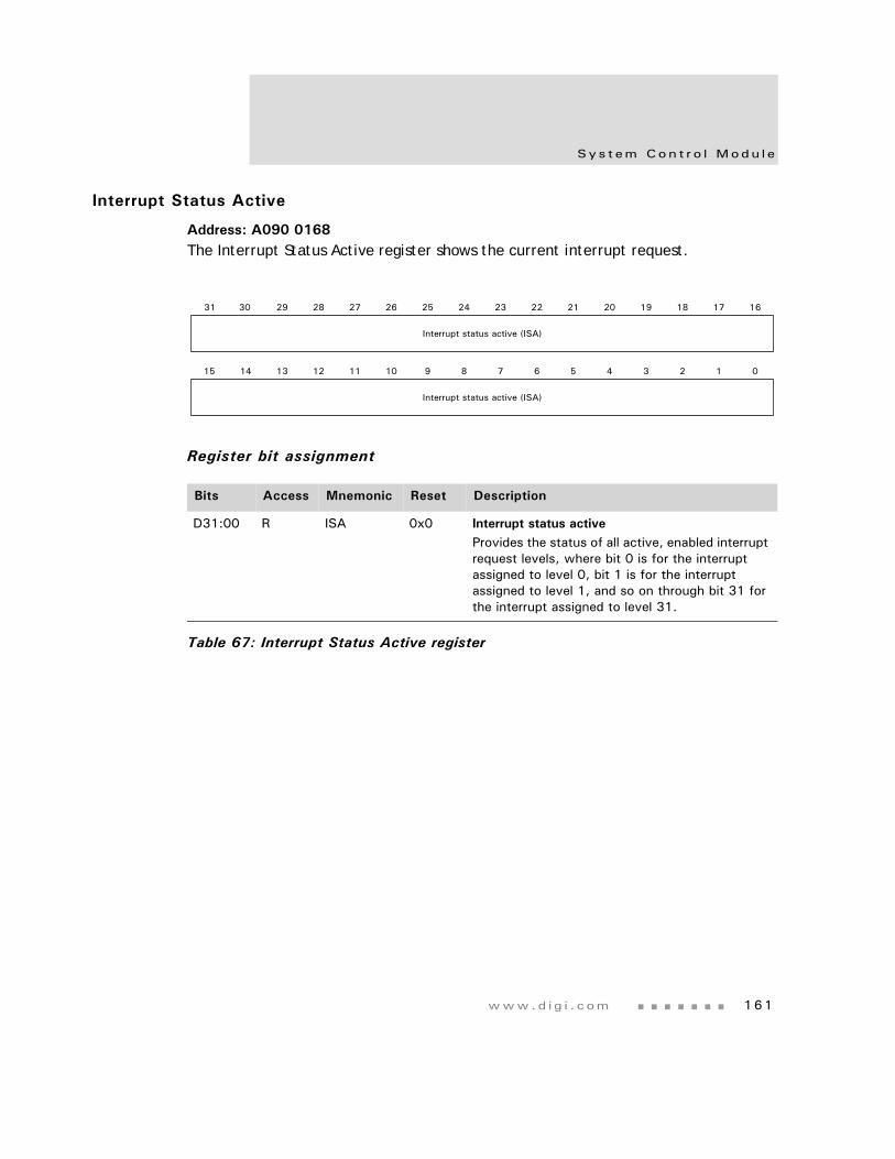
www.d i g i . com 161
Sys t em Con t r o l Modu l e
Interrupt Status Active
Address: A090 0168The Interrupt Status Active register shows the current interrupt request.
Register bit assignment
Bits Access Mnemonic Reset Description
D31:00 R ISA 0x0 Interrupt status activeProvides the status of all active, enabled interrupt request levels, where bit 0 is for the interrupt assigned to level 0, bit 1 is for the interrupt assigned to level 1, and so on through bit 31 for the interrupt assigned to level 31.
Table 67: Interrupt Status Active register
13 12 11 10 9 8 7 6 5 4 3 2 1 015 14
31 29 28 27 26 25 24 23 22 21 20 19 18 17 1630
Interrupt status active (ISA)
Interrupt status active (ISA)
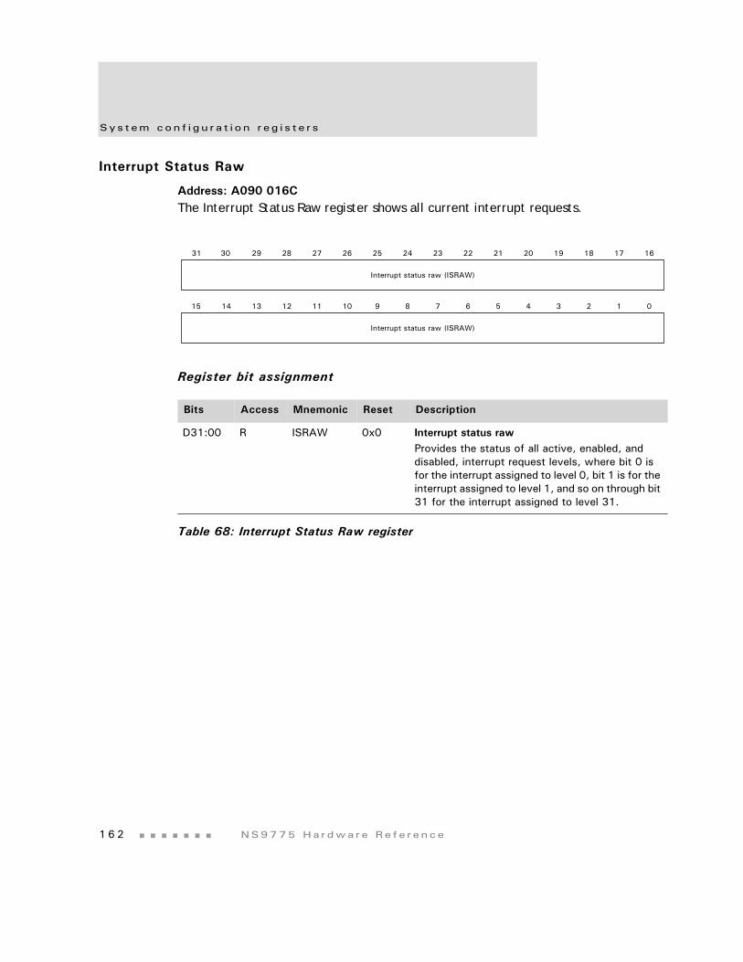
Sys t em con f i g u r a t i o n r e g i s t e r s
1 6 2 NS9775 Ha r dwa r e Re f e r ence
Interrupt Status Raw
Address: A090 016CThe Interrupt Status Raw register shows all current interrupt requests.
Register bit assignment
Bits Access Mnemonic Reset Description
D31:00 R ISRAW 0x0 Interrupt status rawProvides the status of all active, enabled, and disabled, interrupt request levels, where bit 0 is for the interrupt assigned to level 0, bit 1 is for the interrupt assigned to level 1, and so on through bit 31 for the interrupt assigned to level 31.
Table 68: Interrupt Status Raw register
13 12 11 10 9 8 7 6 5 4 3 2 1 015 14
31 29 28 27 26 25 24 23 22 21 20 19 18 17 1630
Interrupt status raw (ISRAW)
Interrupt status raw (ISRAW)
www.d i g i . com 163
Sys t em Con t r o l Modu l e
Timer Interrupt Status register
Address: A090 0170The Timer Interrupt Status register shows all current timer interrupt requests.
Register bit assignment
Software Watchdog Configuration register
Address: A090 0174The Software Watchdog Configuration register configures the software watchdog timer operation.
Bits Access Mnemonic Reset Description
D31:16 N/A Reserved N/A N/A
D15:00 R TIS 0x0 Timer interrupt requests, timer 15–timer 00 Inactive1 Active
Table 69: Timer Interrupt Status register
13 12 11 10 9 8 7 6 5 4 3 2 1 015 14
31 29 28 27 26 25 24 23 22 21 20 19 18 17 1630
Reserved
Timer interrupt requests (TIS)
13 12 11 10 9 8 7 6 5 4 3 2 1 015 14
31 29 28 27 26 25 24 23 22 21 20 19 18 17 1630
Reserved
Reserved SWWE SWWI SWWIC RsvdRsvd SWTCS
Sys t em con f i g u r a t i o n r e g i s t e r s
1 6 4 NS9775 Ha r dwa r e Re f e r ence
Register bit assignment
Bits Access Mnemonic Reset Description
D31:08 N/A Reserved N/A N/A
D07 R/W SWWE 0x0 Software watchdog enable0 Software watchdog disabled1 Software watchdog enabled. Once this is set,
it cannot be cleared.
D06 N/A Reserved N/A N/A
D05 R/W SWWI 0x0 Software watchdog interrupt clearWrite a 1, then a 0 to this bit to clear the software watchdog interrupt.
D04 R/W SWWIC 0x0 Software watchdog interrupt response0 Generate an interrupt1 Generate the reset
D03 N/A Reserved N/A N/A
D02:00 R/W SWTCS 0x0 Software watchdog timer clock select000 CPU clock / 2001 CPU clock / 4010 CPU clock / 8011 CPU clock / 16100 CPU clock / 32101 CPU clock / 64110 Reserved111 Reserved
Table 70: Software Watchdog Configuration register
www.d i g i . com 165
Sys t em Con t r o l Modu l e
Software Watchdog Timer register
Address: A090 0178The Software Watchdog Timer register services the watchdog timer.
Register bit assignment
Clock Configuration register
Address: A090 017CThe Clock Configuration register enables and disables clocks to each module on the AHB bus.
Bits Access Mnemonic Reset Description
D31:00 R/W WT 0x0 Watchdog timer
A read to this register gives the current value of the watchdog timer, but will not change the contents.
A write to the register changes the contents based on the write data value.
Table 71: Software Watchdog Timer register
13 12 11 10 9 8 7 6 5 4 3 2 1 015 14
31 29 28 27 26 25 24 23 22 21 20 19 18 17 1630
Watchdog timer
Watchdog timer
13 12 11 10 9 8 7 6 5 4 3 2 1 015 14
31 29 28 27 26 25 24 23 22 21 20 19 18 17 1630
Reserved
Reserved LPCS LCC MCC PARBCBBC PC MCCJBIG
Sys t em con f i g u r a t i o n r e g i s t e r s
1 6 6 NS9775 Ha r dwa r e Re f e r ence
Register bit assignment
Bits Access Mnemonic Reset Description
D31:10 N/A Reserved N/A N/A
D09:07 R/W LPCS 0x0 LCD panel clock select000 AHB clock001 AHB clock / 2010 AHB clock / 4011 AHB clock / 81xx LCD clock provided by external clock
D06 R/W BBC 0x1 BBus0 Clock disabled1 Clock enabled
D05 R/W LCC 0x1 LCD controller0 Clock disabled1 Clock enabled
D04 R/W MCC 0x1 Memory controller0 Clock disabled1 Clock enabled
D03 R/W PARBC 0x1 PCI arbiter0 Clock disabled1 Clock enabled
D02 R/W PC 0x1 PCI0 Clock disabled1 Clock enabled
D01 R/W JBIGC 0x1 JBIG0 Clock disabled1 Clock enabled
D00 R/W MACC 0x1 Ethernet MAC0 Clock disabled1 Clock enabled
Table 72: Clock Configuration register
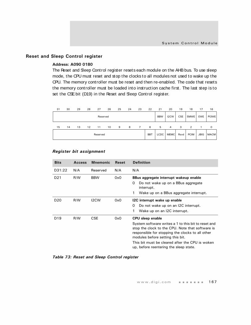
www.d i g i . com 167
Sys t em Con t r o l Modu l e
Reset and Sleep Control register
Address: A090 0180The Reset and Sleep Control register resets each module on the AHB bus. To use sleep mode, the CPU must reset and stop the clocks to all modules not used to wake up the CPU. The memory controller must be reset and then re-enabled. The code that resets the memory controller must be loaded into instruction cache first. The last step is to set the CSE bit (D19) in the Reset and Sleep Control register.
Register bit assignment
Bits Access Mnemonic Reset Definition
D31:22 N/A Reserved N/A N/A
D21 R/W BBW 0x0 BBus aggregate interrupt wakeup enable0 Do not wake up on a BBus aggregate
interrupt.1 Wake up on a BBus aggregate interrupt.
D20 R/W I2CW 0x0 I2C interrupt wake up enable0 Do not wake up on an I2C interrupt.1 Wake up on an I2C interrupt.
D19 R/W CSE 0x0 CPU sleep enableSystem software writes a 1 to this bit to reset and stop the clock to the CPU. Note that software is responsible for stopping the clocks to all other modules before setting this bit. This bit must be cleared after the CPU is woken up, before reentering the sleep state.
Table 73: Reset and Sleep Control register
13 12 11 10 9 8 7 6 5 4 3 2 1 015 14
31 29 28 27 26 25 24 23 22 21 20 19 18 17 1630
Reserved
Reserved LCDC MEMC RsvdBBT PCIM MACMJBIG
I2CW CSE SMWE EWE PI3WEBBW
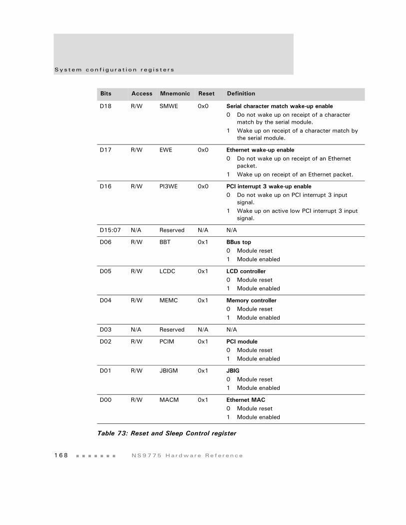
Sys t em con f i g u r a t i o n r e g i s t e r s
1 6 8 NS9775 Ha r dwa r e Re f e r ence
D18 R/W SMWE 0x0 Serial character match wake-up enable0 Do not wake up on receipt of a character
match by the serial module.1 Wake up on receipt of a character match by
the serial module.
D17 R/W EWE 0x0 Ethernet wake-up enable0 Do not wake up on receipt of an Ethernet
packet.1 Wake up on receipt of an Ethernet packet.
D16 R/W PI3WE 0x0 PCI interrupt 3 wake-up enable0 Do not wake up on PCI interrupt 3 input
signal.1 Wake up on active low PCI interrupt 3 input
signal.
D15:07 N/A Reserved N/A N/A
D06 R/W BBT 0x1 BBus top0 Module reset1 Module enabled
D05 R/W LCDC 0x1 LCD controller0 Module reset1 Module enabled
D04 R/W MEMC 0x1 Memory controller0 Module reset1 Module enabled
D03 N/A Reserved N/A N/A
D02 R/W PCIM 0x1 PCI module0 Module reset1 Module enabled
D01 R/W JBIGM 0x1 JBIG0 Module reset1 Module enabled
D00 R/W MACM 0x1 Ethernet MAC0 Module reset1 Module enabled
Bits Access Mnemonic Reset Definition
Table 73: Reset and Sleep Control register
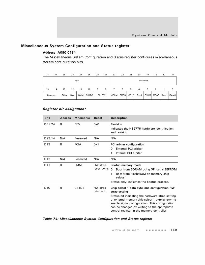
www.d i g i . com 169
Sys t em Con t r o l Modu l e
Miscellaneous System Configuration and Status register
Address: A090 0184The Miscellaneous System Configuration and Status register configures miscellaneous system configuration bits.
Register bit assignment
Bits Access Mnemonic Reset Description
D31:24 R REV 0x0 RevisionIndicates the NS9775 hardware identification and revision.
D23:14 N/A Reserved N/A N/A
D13 R PCIA 0x1 PCI arbiter configuration0 External PCI arbiter1 Internal PCI arbiter
D12 N/A Reserved N/A N/A
D11 R BMM HW strap reset_done
Bootup memory mode0 Boot from SDRAM using SPI serial EEPROM1 Boot from Flash/ROM on memory chip
select 1Status only; indicates the bootup process.
D10 R CS1DB HW strap print_out
Chip select 1 data byte lane configuration HW strap settingStatus bit indicating the hardware strap setting of external memory chip select 1 byte lane/write enable signal configuration. This configuration can be changed by writing to the appropriate control register in the memory controller.
Table 74: Miscellaneous System Configuration and Status register
PCIA Rsvd CS1DBBMM CS1DW MCCM PMSS CS1P Rsvd ENDM MBAR Rsvd IRAM0
13 12 11 10 9 8 7 6 5 4 3 2 1 015 14
31 29 28 27 26 25 24 23 22 21 20 19 18 17 1630
REV Reserved
Reserved
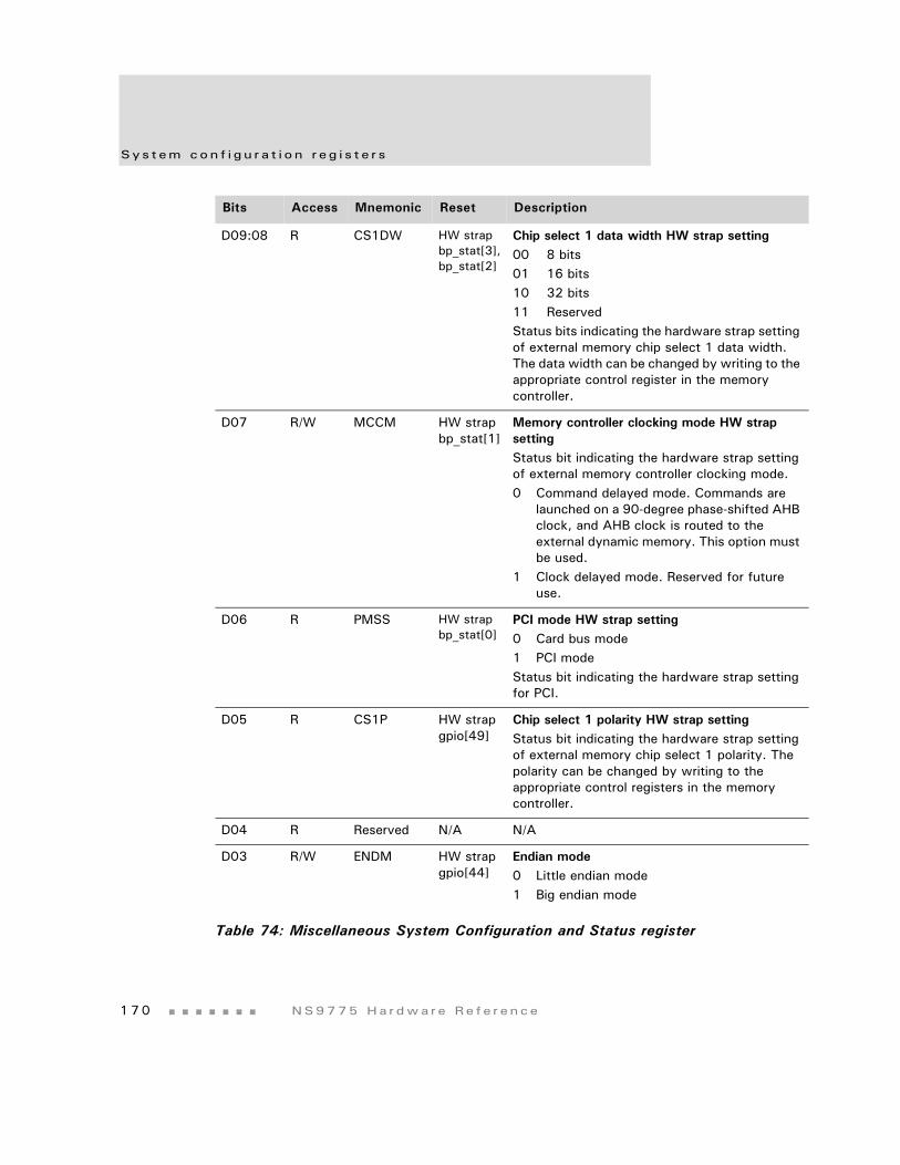
Sys t em con f i g u r a t i o n r e g i s t e r s
1 7 0 NS9775 Ha r dwa r e Re f e r ence
D09:08 R CS1DW HW strap bp_stat[3], bp_stat[2]
Chip select 1 data width HW strap setting00 8 bits01 16 bits10 32 bits11 ReservedStatus bits indicating the hardware strap setting of external memory chip select 1 data width. The data width can be changed by writing to the appropriate control register in the memory controller.
D07 R/W MCCM HW strap bp_stat[1]
Memory controller clocking mode HW strap settingStatus bit indicating the hardware strap setting of external memory controller clocking mode.0 Command delayed mode. Commands are
launched on a 90-degree phase-shifted AHB clock, and AHB clock is routed to the external dynamic memory. This option must be used.
1 Clock delayed mode. Reserved for future use.
D06 R PMSS HW strap bp_stat[0]
PCI mode HW strap setting0 Card bus mode1 PCI modeStatus bit indicating the hardware strap setting for PCI.
D05 R CS1P HW strap gpio[49]
Chip select 1 polarity HW strap settingStatus bit indicating the hardware strap setting of external memory chip select 1 polarity. The polarity can be changed by writing to the appropriate control registers in the memory controller.
D04 R Reserved N/A N/A
D03 R/W ENDM HW strap gpio[44]
Endian mode0 Little endian mode1 Big endian mode
Bits Access Mnemonic Reset Description
Table 74: Miscellaneous System Configuration and Status register
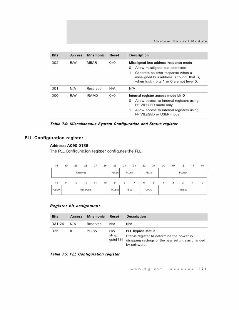
www.d i g i . com 171
Sys t em Con t r o l Modu l e
PLL Configuration register
Address: A090 0188The PLL Configuration register configures the PLL.
Register bit assignment
D02 R/W MBAR 0x0 Misaligned bus address response mode0 Allow misaligned bus addresses1 Generate an error response when a
misaligned bus address is found; that is, when haddr bits 1 or 0 are not level 0.
D01 N/A Reserved N/A N/A
D00 R/W IRAM0 0x0 Internal register access mode bit 00 Allow access to internal registers using
PRIVILEGED mode only1 Allow access to internal registers using
PRIVILEGED or USER mode.
Bits Access Mnemonic Reset Description
Table 74: Miscellaneous System Configuration and Status register
Bits Access Mnemonic Reset Description
D31:26 N/A Reserved N/A N/A
D25 R PLLBS HW strap gpio[19]
PLL bypass statusStatus register to determine the powerup strapping settings or the new settings as changed by software.
Table 75: PLL Configuration register
PLLBW FSEL CPCC NDSW
13 12 11 10 9 8 7 6 5 4 3 2 1 015 14
PLLSW
31 29 28 27 26 25 24 23 22 21 20 19 18 17 1630
PLLBS PLLFS PLLIS PLLNDReserved
Reserved
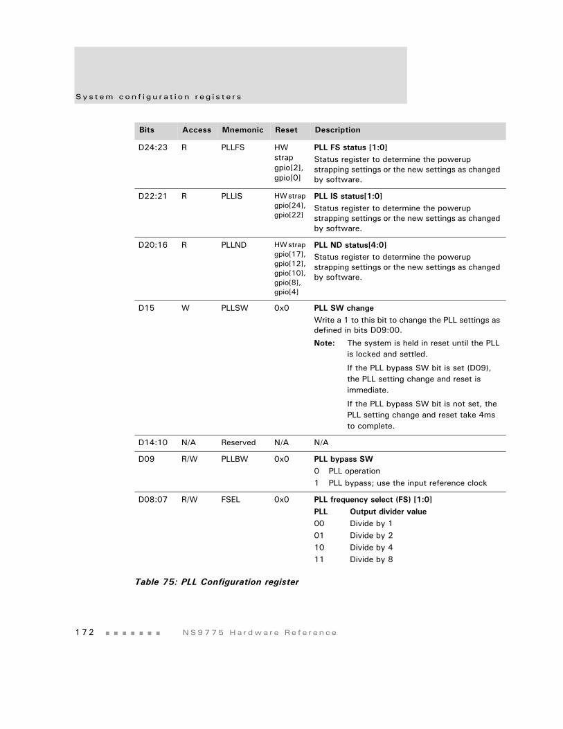
Sys t em con f i g u r a t i o n r e g i s t e r s
1 7 2 NS9775 Ha r dwa r e Re f e r ence
D24:23 R PLLFS HW strap gpio[2], gpio[0]
PLL FS status [1:0]Status register to determine the powerup strapping settings or the new settings as changed by software.
D22:21 R PLLIS HW strap gpio[24], gpio[22]
PLL IS status[1:0]Status register to determine the powerup strapping settings or the new settings as changed by software.
D20:16 R PLLND HW strap gpio[17], gpio[12], gpio[10], gpio[8], gpio[4]
PLL ND status[4:0]Status register to determine the powerup strapping settings or the new settings as changed by software.
D15 W PLLSW 0x0 PLL SW changeWrite a 1 to this bit to change the PLL settings as defined in bits D09:00.
Note: The system is held in reset until the PLL is locked and settled.
If the PLL bypass SW bit is set (D09), the PLL setting change and reset is immediate.
If the PLL bypass SW bit is not set, the PLL setting change and reset take 4ms to complete.
D14:10 N/A Reserved N/A N/A
D09 R/W PLLBW 0x0 PLL bypass SW0 PLL operation1 PLL bypass; use the input reference clock
D08:07 R/W FSEL 0x0 PLL frequency select (FS) [1:0]PLL Output divider value00 Divide by 101 Divide by 210 Divide by 411 Divide by 8
Bits Access Mnemonic Reset Description
Table 75: PLL Configuration register
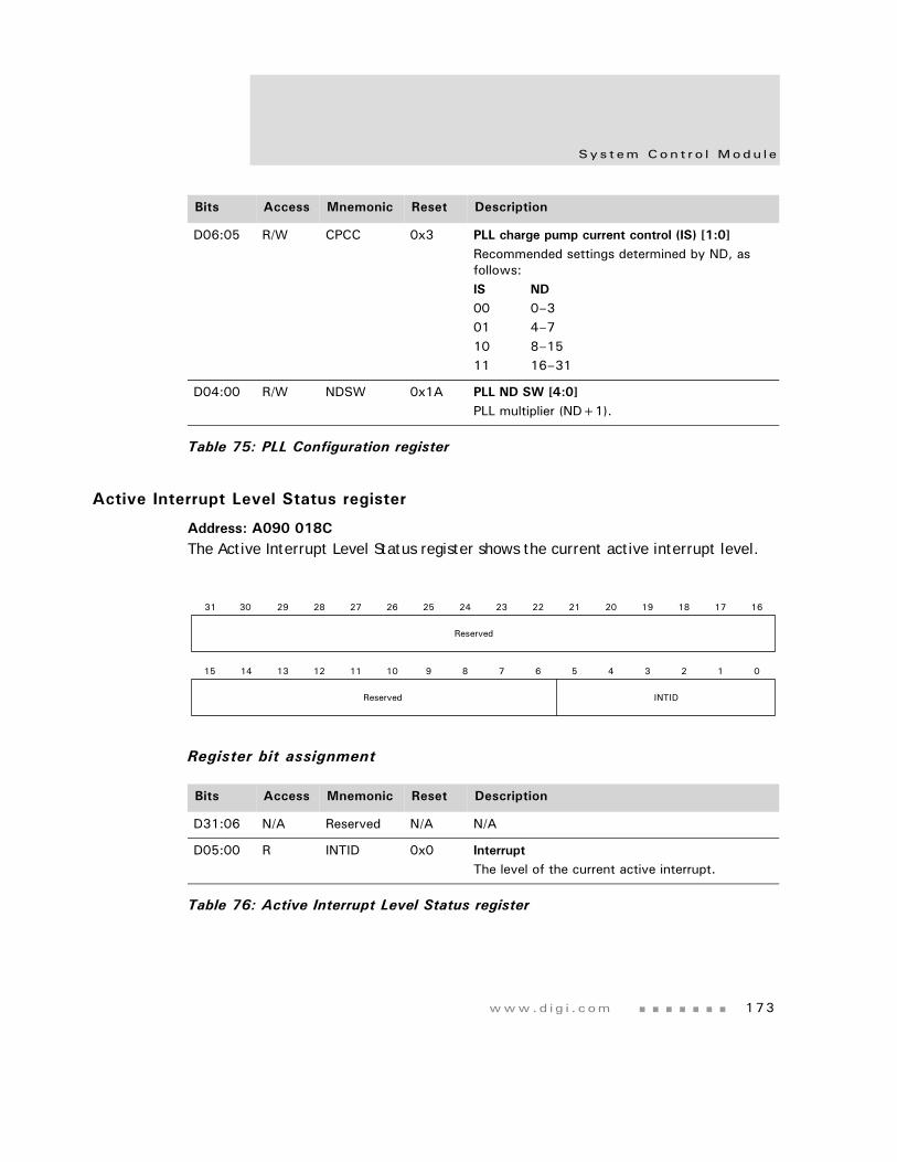
www.d i g i . com 173
Sys t em Con t r o l Modu l e
Active Interrupt Level Status register
Address: A090 018CThe Active Interrupt Level Status register shows the current active interrupt level.
Register bit assignment
D06:05 R/W CPCC 0x3 PLL charge pump current control (IS) [1:0]Recommended settings determined by ND, as follows:IS ND00 0–301 4–710 8–1511 16–31
D04:00 R/W NDSW 0x1A PLL ND SW [4:0]PLL multiplier (ND+1).
Bits Access Mnemonic Reset Description
Table 75: PLL Configuration register
Bits Access Mnemonic Reset Description
D31:06 N/A Reserved N/A N/A
D05:00 R INTID 0x0 InterruptThe level of the current active interrupt.
Table 76: Active Interrupt Level Status register
13 12 11 10 9 8 7 6 5 4 3 2 1 015 14
31 29 28 27 26 25 24 23 22 21 20 19 18 17 1630
Reserved
Reserved INTID
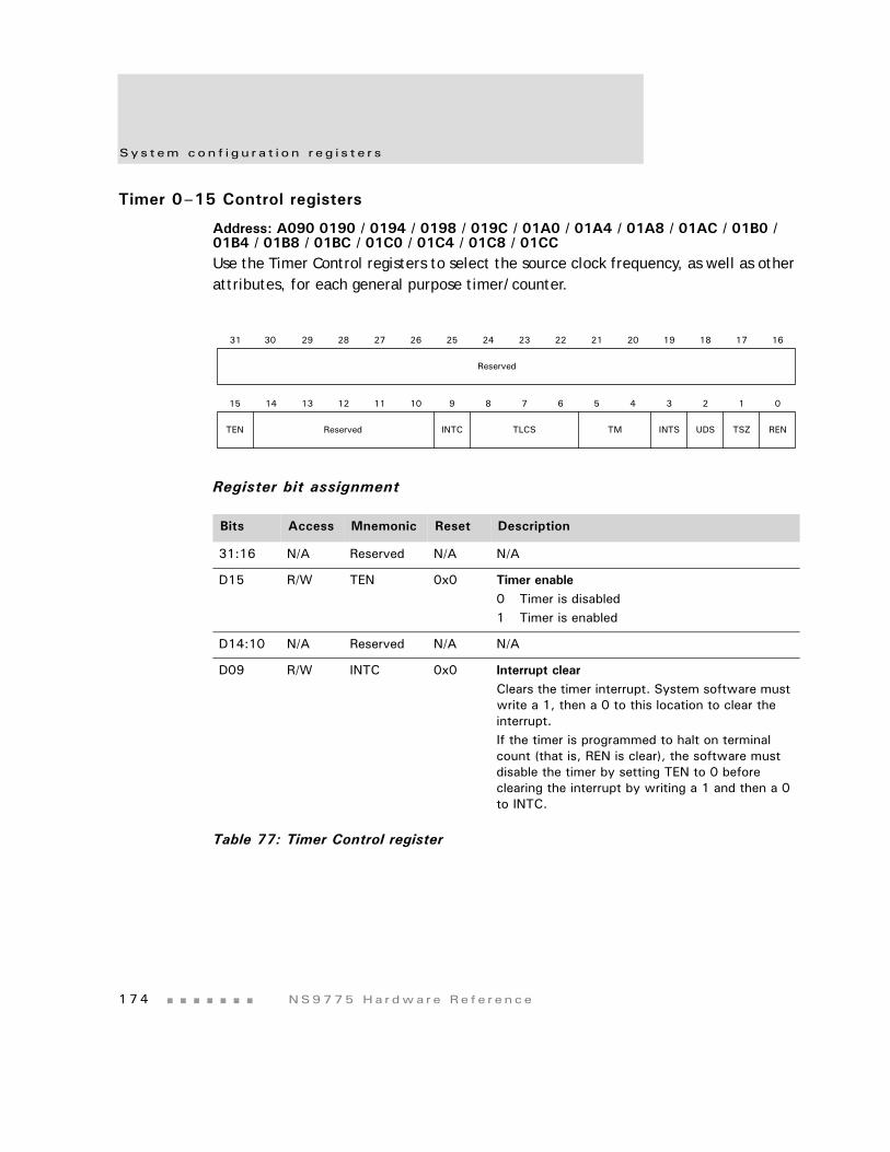
Sys t em con f i g u r a t i o n r e g i s t e r s
1 7 4 NS9775 Ha r dwa r e Re f e r ence
Timer 0–15 Control registers
Address: A090 0190 / 0194 / 0198 / 019C / 01A0 / 01A4 / 01A8 / 01AC / 01B0 / 01B4 / 01B8 / 01BC / 01C0 / 01C4 / 01C8 / 01CCUse the Timer Control registers to select the source clock frequency, as well as other attributes, for each general purpose timer/counter.
Register bit assignment
Bits Access Mnemonic Reset Description
31:16 N/A Reserved N/A N/A
D15 R/W TEN 0x0 Timer enable0 Timer is disabled1 Timer is enabled
D14:10 N/A Reserved N/A N/A
D09 R/W INTC 0x0 Interrupt clearClears the timer interrupt. System software must write a 1, then a 0 to this location to clear the interrupt.If the timer is programmed to halt on terminal count (that is, REN is clear), the software must disable the timer by setting TEN to 0 before clearing the interrupt by writing a 1 and then a 0 to INTC.
Table 77: Timer Control register
13 12 11 10 9 8 7 6 5 4 3 2 1 015 14
31 29 28 27 26 25 24 23 22 21 20 19 18 17 1630
Reserved
ReservedTEN INTC TLCS TM INTS UDS TSZ REN
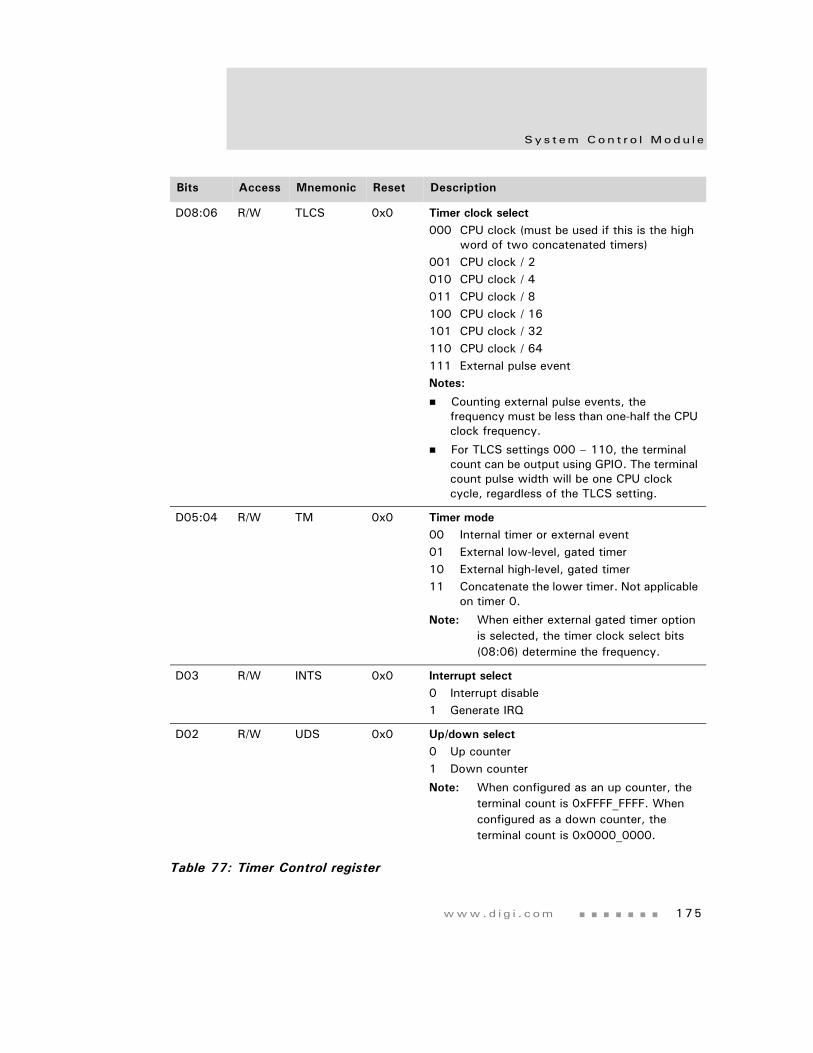
www.d i g i . com 175
Sys t em Con t r o l Modu l e
D08:06 R/W TLCS 0x0 Timer clock select000 CPU clock (must be used if this is the high
word of two concatenated timers)001 CPU clock / 2010 CPU clock / 4011 CPU clock / 8100 CPU clock / 16101 CPU clock / 32110 CPU clock / 64111 External pulse eventNotes:
Counting external pulse events, the frequency must be less than one-half the CPU clock frequency.
For TLCS settings 000 – 110, the terminal count can be output using GPIO. The terminal count pulse width will be one CPU clock cycle, regardless of the TLCS setting.
D05:04 R/W TM 0x0 Timer mode00 Internal timer or external event01 External low-level, gated timer10 External high-level, gated timer11 Concatenate the lower timer. Not applicable
on timer 0.
Note: When either external gated timer option is selected, the timer clock select bits (08:06) determine the frequency.
D03 R/W INTS 0x0 Interrupt select0 Interrupt disable1 Generate IRQ
D02 R/W UDS 0x0 Up/down select0 Up counter1 Down counter
Note: When configured as an up counter, the terminal count is 0xFFFF_FFFF. When configured as a down counter, the terminal count is 0x0000_0000.
Bits Access Mnemonic Reset Description
Table 77: Timer Control register
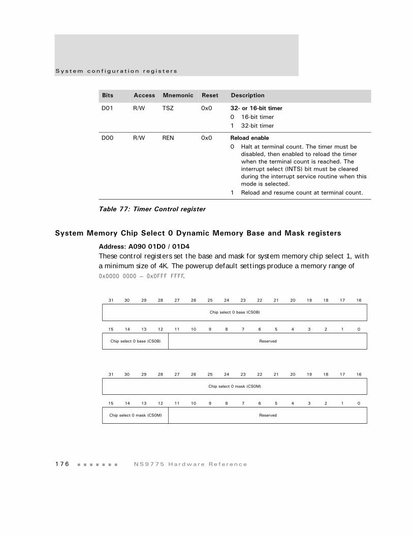
Sys t em con f i g u r a t i o n r e g i s t e r s
1 7 6 NS9775 Ha r dwa r e Re f e r ence
System Memory Chip Select 0 Dynamic Memory Base and Mask registers
Address: A090 01D0 / 01D4These control registers set the base and mask for system memory chip select 1, with a minimum size of 4K. The powerup default settings produce a memory range of0x0000 0000 — 0x0FFF FFFF.
D01 R/W TSZ 0x0 32- or 16-bit timer0 16-bit timer1 32-bit timer
D00 R/W REN 0x0 Reload enable0 Halt at terminal count. The timer must be
disabled, then enabled to reload the timer when the terminal count is reached. The interrupt select (INTS) bit must be cleared during the interrupt service routine when this mode is selected.
1 Reload and resume count at terminal count.
Bits Access Mnemonic Reset Description
Table 77: Timer Control register
13 12 11 10 9 8 7 6 5 4 3 2 1 015 14
31 29 28 27 26 25 24 23 22 21 20 19 18 17 1630
Chip select 0 base (CS0B)
ReservedChip select 0 base (CS0B)
13 12 11 10 9 8 7 6 5 4 3 2 1 015 14
31 29 28 27 26 25 24 23 22 21 20 19 18 17 1630
Chip select 0 mask (CS0M)
ReservedChip select 0 mask (CS0M)

www.d i g i . com 177
Sys t em Con t r o l Modu l e
Register bit assignment
System Memory Chip Select 1 Dynamic Memory Base and Mask registers
Address: A090 01D8 / 01DCThese control registers set the base and mask for system memory chip select 1, with a minimum size of 4K. The powerup default settings produce a memory range of0x1000 0000 — 0x1FFF FFFF.
Bits Access Mnemonic Reset Description
D31:12 R/W CS0B 0x00000 Chip select 0 baseBase address for chip select 0 (dynamic).
D11:00 N/A Reserved N/A N/A
D31:12 R/W CS0M 0xF0000 Chip select 0 maskMask or size for chip select 0 (dynamic).
D11:00 N/A Reserved N/A N/A
Table 78: System Memory Chip Select 0 Dynamic Memory Base & Mask registers
13 12 11 10 9 8 7 6 5 4 3 2 1 015 14
31 29 28 27 26 25 24 23 22 21 20 19 18 17 1630
Chip select 1 base (CS1B)
ReservedChip select 1 base (CS1B)
13 12 11 10 9 8 7 6 5 4 3 2 1 015 14
31 29 28 27 26 25 24 23 22 21 20 19 18 17 1630
Chip select 1 mask (CS1M)
ReservedChip select 1 mask (CS1M)
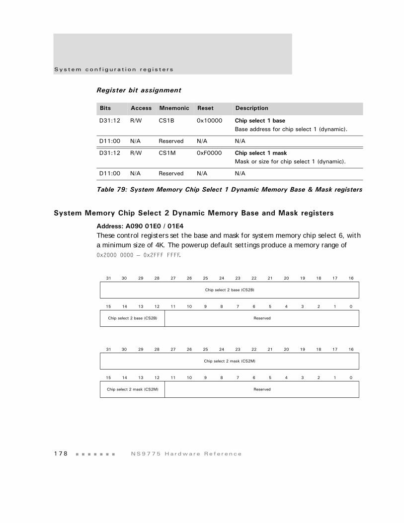
Sys t em con f i g u r a t i o n r e g i s t e r s
1 7 8 NS9775 Ha r dwa r e Re f e r ence
Register bit assignment
System Memory Chip Select 2 Dynamic Memory Base and Mask registers
Address: A090 01E0 / 01E4These control registers set the base and mask for system memory chip select 6, with a minimum size of 4K. The powerup default settings produce a memory range of0x2000 0000 — 0x2FFF FFFF.
Bits Access Mnemonic Reset Description
D31:12 R/W CS1B 0x10000 Chip select 1 baseBase address for chip select 1 (dynamic).
D11:00 N/A Reserved N/A N/A
D31:12 R/W CS1M 0xF0000 Chip select 1 maskMask or size for chip select 1 (dynamic).
D11:00 N/A Reserved N/A N/A
Table 79: System Memory Chip Select 1 Dynamic Memory Base & Mask registers
13 12 11 10 9 8 7 6 5 4 3 2 1 015 14
31 29 28 27 26 25 24 23 22 21 20 19 18 17 1630
Chip select 2 base (CS2B)
ReservedChip select 2 base (CS2B)
13 12 11 10 9 8 7 6 5 4 3 2 1 015 14
31 29 28 27 26 25 24 23 22 21 20 19 18 17 1630
Chip select 2 mask (CS2M)
ReservedChip select 2 mask (CS2M)
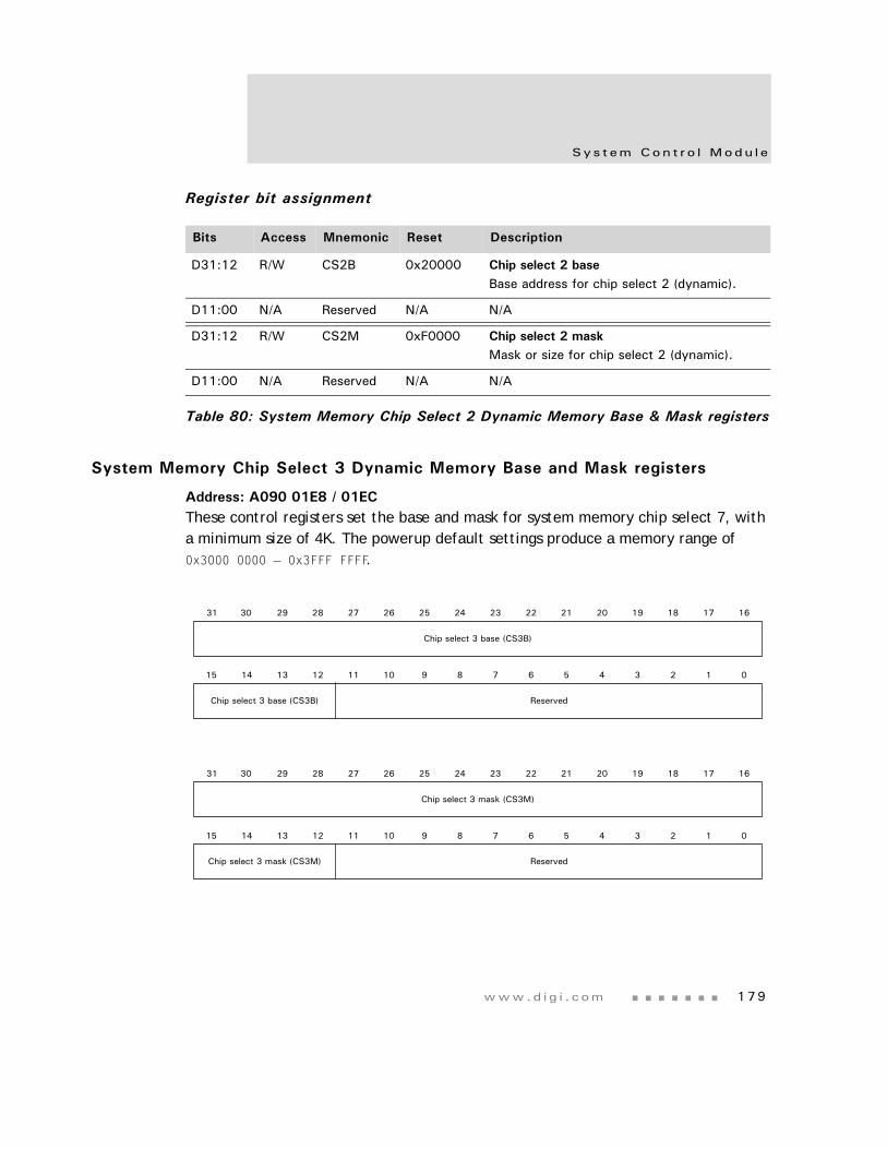
www.d i g i . com 179
Sys t em Con t r o l Modu l e
Register bit assignment
System Memory Chip Select 3 Dynamic Memory Base and Mask registers
Address: A090 01E8 / 01ECThese control registers set the base and mask for system memory chip select 7, with a minimum size of 4K. The powerup default settings produce a memory range of 0x3000 0000 — 0x3FFF FFFF.
Bits Access Mnemonic Reset Description
D31:12 R/W CS2B 0x20000 Chip select 2 baseBase address for chip select 2 (dynamic).
D11:00 N/A Reserved N/A N/A
D31:12 R/W CS2M 0xF0000 Chip select 2 maskMask or size for chip select 2 (dynamic).
D11:00 N/A Reserved N/A N/A
Table 80: System Memory Chip Select 2 Dynamic Memory Base & Mask registers
13 12 11 10 9 8 7 6 5 4 3 2 1 015 14
31 29 28 27 26 25 24 23 22 21 20 19 18 17 1630
Chip select 3 base (CS3B)
ReservedChip select 3 base (CS3B)
13 12 11 10 9 8 7 6 5 4 3 2 1 015 14
31 29 28 27 26 25 24 23 22 21 20 19 18 17 1630
Chip select 3 mask (CS3M)
ReservedChip select 3 mask (CS3M)

Sys t em con f i g u r a t i o n r e g i s t e r s
1 8 0 NS9775 Ha r dwa r e Re f e r ence
Register bit assignment
System Memory Chip Select 0 Static Memory Base and Mask registers
Address: A090 01F0 / 01F4These control registers set the base and mask for system memory chip select 0, with a minimum size of 4K. The powerup default settings produce a memory range of0x4000 0000 — 0x4FFF FFFF.
Bits Access Mnemonic Reset Description
D31:12 R/W CS3B 0x30000 Chip select 3 baseBase address for chip select 3 (dynamic).
D11:00 N/A Reserved N/A N/A
D31:12 R/W CS3M 0xF0000 Chip select 3 maskMask or size for chip select 3 (dynamic).
D11:00 N/A Reserved N/A N/A
Table 81: System Memory Chip Select 3 Dynamic Memory Base & Mask registers
13 12 11 10 9 8 7 6 5 4 3 2 1 015 14
31 29 28 27 26 25 24 23 22 21 20 19 18 17 1630
Chip select 0 base (CS0B)
ReservedChip select 0 base (CS0B)
13 12 11 10 9 8 7 6 5 4 3 2 1 015 14
31 29 28 27 26 25 24 23 22 21 20 19 18 17 1630
Chip select 0 mask (CS0M)
ReservedChip select 0 mask (CS0M)

www.d i g i . com 181
Sys t em Con t r o l Modu l e
Register bit assignment
System Memory Chip Select 1 Static Memory Base and Mask registers
Address: A09001F8 / 01FCThese control registers set the base and mask for system memory chip select 1, with a minimum size of 4K. The powerup default settings produce a memory range of0x5000 0000 — 0x5FFF FFFF.
Bits Access Mnemonic Reset Description
D31:12 R/W CS0B 0x40000 Chip select 0 baseBase address for chip select 0 (static).
D11:00 N/A Reserved N/A N/A
D31:12 R/W CS0M 0xF0000 Chip select 0 maskMask or size for chip select 0 (static).
D11:00 N/A Reserved N/A N/A
Table 82: System Memory Chip Select 0 Static Memory Base & Mask registers
13 12 11 10 9 8 7 6 5 4 3 2 1 015 14
31 29 28 27 26 25 24 23 22 21 20 19 18 17 1630
Chip select 1 base (CS1B)
ReservedChip select 1 base (CS1B)
13 12 11 10 9 8 7 6 5 4 3 2 1 015 14
31 29 28 27 26 25 24 23 22 21 20 19 18 17 1630
Chip select 1 mask (CS1M)
ReservedChip select 1 mask (CS1M)
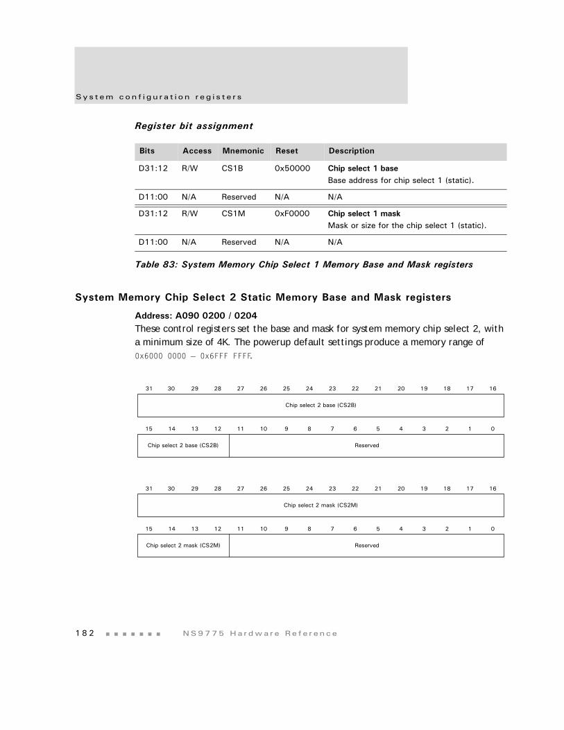
Sys t em con f i g u r a t i o n r e g i s t e r s
1 8 2 NS9775 Ha r dwa r e Re f e r ence
Register bit assignment
System Memory Chip Select 2 Static Memory Base and Mask registers
Address: A090 0200 / 0204These control registers set the base and mask for system memory chip select 2, with a minimum size of 4K. The powerup default settings produce a memory range of0x6000 0000 — 0x6FFF FFFF.
Bits Access Mnemonic Reset Description
D31:12 R/W CS1B 0x50000 Chip select 1 baseBase address for chip select 1 (static).
D11:00 N/A Reserved N/A N/A
D31:12 R/W CS1M 0xF0000 Chip select 1 maskMask or size for the chip select 1 (static).
D11:00 N/A Reserved N/A N/A
Table 83: System Memory Chip Select 1 Memory Base and Mask registers
13 12 11 10 9 8 7 6 5 4 3 2 1 015 14
31 29 28 27 26 25 24 23 22 21 20 19 18 17 1630
Chip select 2 base (CS2B)
ReservedChip select 2 base (CS2B)
13 12 11 10 9 8 7 6 5 4 3 2 1 015 14
31 29 28 27 26 25 24 23 22 21 20 19 18 17 1630
Chip select 2 mask (CS2M)
ReservedChip select 2 mask (CS2M)
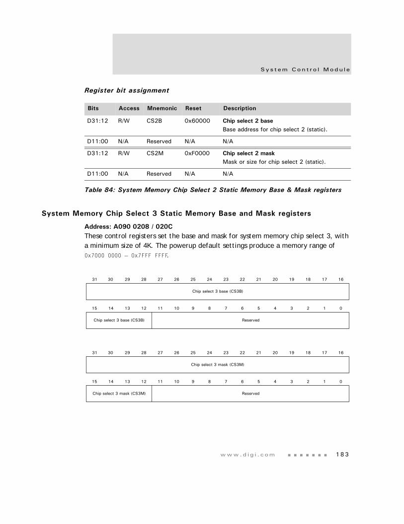
www.d i g i . com 183
Sys t em Con t r o l Modu l e
Register bit assignment
System Memory Chip Select 3 Static Memory Base and Mask registers
Address: A090 0208 / 020CThese control registers set the base and mask for system memory chip select 3, with a minimum size of 4K. The powerup default settings produce a memory range of0x7000 0000 — 0x7FFF FFFF.
Bits Access Mnemonic Reset Description
D31:12 R/W CS2B 0x60000 Chip select 2 baseBase address for chip select 2 (static).
D11:00 N/A Reserved N/A N/A
D31:12 R/W CS2M 0xF0000 Chip select 2 maskMask or size for chip select 2 (static).
D11:00 N/A Reserved N/A N/A
Table 84: System Memory Chip Select 2 Static Memory Base & Mask registers
13 12 11 10 9 8 7 6 5 4 3 2 1 015 14
31 29 28 27 26 25 24 23 22 21 20 19 18 17 1630
Chip select 3 base (CS3B)
ReservedChip select 3 base (CS3B)
13 12 11 10 9 8 7 6 5 4 3 2 1 015 14
31 29 28 27 26 25 24 23 22 21 20 19 18 17 1630
Chip select 3 mask (CS3M)
ReservedChip select 3 mask (CS3M)
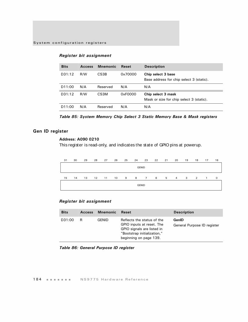
Sys t em con f i g u r a t i o n r e g i s t e r s
1 8 4 NS9775 Ha r dwa r e Re f e r ence
Register bit assignment
Gen ID register
Address: A090 0210This register is read-only, and indicates the state of GPIO pins at powerup.
Register bit assignment
Bits Access Mnemonic Reset Description
D31:12 R/W CS3B 0x70000 Chip select 3 baseBase address for chip select 3 (static).
D11:00 N/A Reserved N/A N/A
D31:12 R/W CS3M 0xF0000 Chip select 3 maskMask or size for chip select 3 (static).
D11:00 N/A Reserved N/A N/A
Table 85: System Memory Chip Select 3 Static Memory Base & Mask registers
Bits Access Mnemonic Reset Description
D31:00 R GENID Reflects the status of the GPIO inputs at reset. The GPIO signals are listed in "Bootstrap initialization," beginning on page 139.
GenIDGeneral Purpose ID register
Table 86: General Purpose ID register
13 12 11 10 9 8 7 6 5 4 3 2 1 015 14
31 29 28 27 26 25 24 23 22 21 20 19 18 17 1630
GENID
GENID
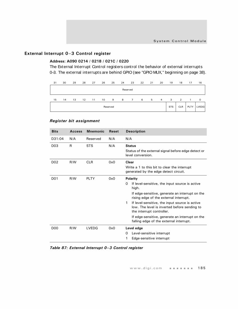
www.d i g i . com 185
Sys t em Con t r o l Modu l e
External Interrupt 0–3 Control register
Address: A090 0214 / 0218 / 021C / 0220The External Interrupt Control registers control the behavior of external interrupts0–3. The external interrupts are behind GPIO (see "GPIO MUX," beginning on page 38).
Register bit assignment
Bits Access Mnemonic Reset Description
D31:04 N/A Reserved N/A N/A
D03 R STS N/A StatusStatus of the external signal before edge detect or level conversion.
D02 R/W CLR 0x0 ClearWrite a 1 to this bit to clear the interrupt generated by the edge detect circuit.
D01 R/W PLTY 0x0 Polarity0 If level-sensitive, the input source is active
high.
If edge-sensitive, generate an interrupt on the rising edge of the external interrupt.
1 If level-sensitive, the input source is active low. The level is inverted before sending to the interrupt controller.
If edge-sensitive, generate an interrupt on the falling edge of the external interrupt.
D00 R/W LVEDG 0x0 Level edge0 Level-sensitive interrupt1 Edge-sensitive interrupt
Table 87: External Interrupt 0–3 Control register
13 12 11 10 9 8 7 6 5 4 3 2 1 015 14
31 29 28 27 26 25 24 23 22 21 20 19 18 17 1630
Reserved
Reserved STS CLR PLTY LVEDG

187
Memory ControllerC H A P T E R 5
The Multiport Memory Controller is an AMBA-compliant system-on-chip (SoC) peripheral that connects to the Advanced High-performance Bus (AHB). The remainder of this chapter refers to this controller as the memory controller.
Fea t u r e s
1 8 8 NS9775 Ha r dwa r e Re f e r ence
Features
The memory controller provides these features:
AMBA 32-bit AHB compliancy.
Dynamic memory interface support including SDRAM and JEDEC low-power SDRAM.
Asynchronous static memory device support including RAM, ROM, and Flash, with and without asynchronous page mode.
Can operate with cached processors with copyback caches.
Can operate with uncached processors.
Low transaction latency.
Read and write buffers to reduce latency and improve performance, particularly for uncached processors.
8-bit, 16-bit, and 32-bit wide static memory support.
16-bit and 32-bit wide chip select SDRAM memory support.
Static memory features, such as:
– Asynchronous page mode read
– Programmable wait states
– Bus turnaround delay
– Output enable and write enable delays
– Extended wait
Power-saving modes that dynamically control SDRAM clk_en.
Dynamic memory self-refresh mode supported by a power management unit (PMU) interface or by software.
Controller supports 2K, 4K, and 8K row address synchronous memory parts; that is, typical 512 MB, 256 MB, and 16 Mb parts with 8, 16, or 32 DQ bits per device.
A separate AHB interface to program the memory controller. This enables the memory controller registers to be situated in memory with other system peripheral registers.
Locked AHB transaction support.
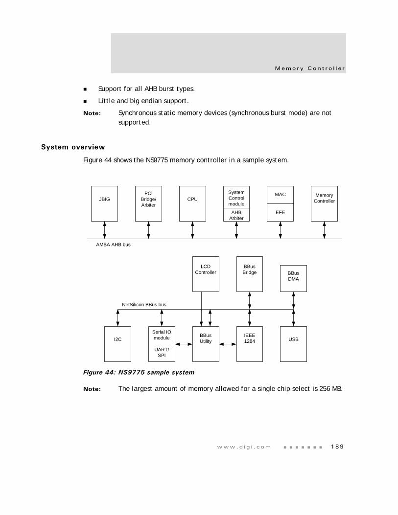
www.d i g i . com 189
Memo ry Con t r o l l e r
Support for all AHB burst types.
Little and big endian support.
Note: Synchronous static memory devices (synchronous burst mode) are not supported.
System overview
Figure 44 shows the NS9775 memory controller in a sample system.
Figure 44: NS9775 sample system
Note: The largest amount of memory allowed for a single chip select is 256 MB.
LCD Controller
BBus Bridge BBus
DMA
I2CSerial IO module
UART/SPI
BBus Utility
IEEE 1284 USB
AMBA AHB bus
NetSilicon BBus bus
PCI Bridge/Arbiter
CPUSystem Control module
AHB Arbiter
MAC
EFE
Memory ControllerJBIG
Fea t u r e s
1 9 0 NS9775 Ha r dwa r e Re f e r ence
Low-power operation
In many systems, the contents of the memory system have to be maintained during low-power sleep modes. NS9775 provides two features to enable this:
Dynamic memory refresh over soft reset
A mechanism to place the dynamic memories into self-refresh mode
Self-refresh mode can be entered as follows:
1 Set the SREFREQ bit in the Dynamic Memory Control register (see page 282).
2 Poll the SREFACK bit in the Status register (see page 280).
Note: Static memory can be accessed as normal when the SDRAM memory is in self-refresh mode.
Low-power SDRAM partial array refresh
The memory controller supports JEDEC low-power SDRAM partial array refresh. Partial array refresh can be programmed by initializing the SDRAM memory device appropriately. When the memory device is put into self-refresh mode, only the memory banks specified are refreshed. The memory banks that are not refreshed lose their data contents.
Memory map
The memory controller provides hardware support for booting from external nonvolatile memory. During booting, the nonvolatile memory must be located at address 0x00000000 in memory. When the system is booted, the SRAM or SDRAM memory can be remapped to address 0x00000000 by modifying the address map in the AHB decoder.
Power-on reset memory map
On power-on reset, memory chip select 1 is mirrored onto memory chip select 0 and chip select 4. Any transactions to memory chip select 0 or chip select 4 (or chip select 1), then, access memory chip select 1. Clearing the address mirror bit (M) in the Control register (see page 278) disables address mirroring, and memory chip select 0, chip select 4, and memory chip select 1 can be accessed as normal.
www.d i g i . com 191
Memo ry Con t r o l l e r
Chip select 1 memory configuration
You can configure the memory width and chip select polarity of static memory chip select 1 by using selected input signals. This allows you to boot from chip select 1.
These are the bootstrap signals:
boot_strap[4:3]: Memory width select
gpio[49]: Chip select polarity
boot_strap[0]: Byte lane enable_n/write_enable_n for byte-wide devices
Example: Boot from flash, SRAM mapped after boot
The system is set up as:
Chip select 1 is connected to the boot flash device.
Chip select 0 is connected to the SRAM to be remapped to 0x00000000 after boot.
The boot sequence is as follows:
1 At power-on, the reset chip select 1 is mirrored into chip select 0 (and chip select 4). The following signals are configured so the nonvolatile memory device can be accessed:– boot_strap[4:3]
– gpio[49]
2 When the power-on reset (reset_n) and AHB reset (HRESETn) go inactive, the processor starts booting from 0x00000000 in memory.
3 The software programs the optimum delay values in the flash memory so the boot code can run at full speed.
4 The code branches to chip select 1 so the code can continue executing from the non-remapped memory location.
5 The appropriate values are programmed into the memory controller to configure chip select 0.
6 The address mirroring is disabled by clearing the address mirror (M) field in the Control register (see page 278).
7 The ARM reset and interrupt vectors are copied from flash memory to SRAM that can then be accessed at address 0x00000000.
8 More boot, initialization, or application code is executed.
S t a t i c memo ry con t r o l l e r
1 9 2 NS9775 Ha r dwa r e Re f e r ence
Example: Boot from flash, SDRAM remapped after boot
The system is set up as:
Chip select 1 is connected to the boot flash device.
Chip select 4 is connected to the SDRAM to be remapped to 0x00000000 after boot.
The boot sequence is as follows:
1 At power-on, the reset chip select 1 is mirrored into chip select 4 (and chip select 0). The following signals are configured so the nonvolatile memory device can be accessed:– boot_strap[4:3]
– gpio[49]
2 When the power-on reset (reset_n) and AHB reset (HRESETn) go inactive, the processor starts booting from 0x00000000 in memory.
3 The software programs the optimum delay values in flash memory so the boot code can run at full speed.
4 The code branches to chip select 1 so the code can continue executing from the non-remapped memory location.
5 The appropriate values are programmed into the memory controller to configure chip select 4, and the memory device is initialized.
6 The address mirroring is disabled by clearing the address mirror (M) field in the Control register (see page 278).
7 The ARM reset and interrupt vectors are copied from flash memory to SDRAM that can then be accessed at address 0x00000000.
8 More boot, initialization, or application code is executed.
Static memory controller
Table 88 shows configurations for the static memory controller with different types of memory devices. See "Static Memory Configuration 0–3 registers" on page 303 for more information.
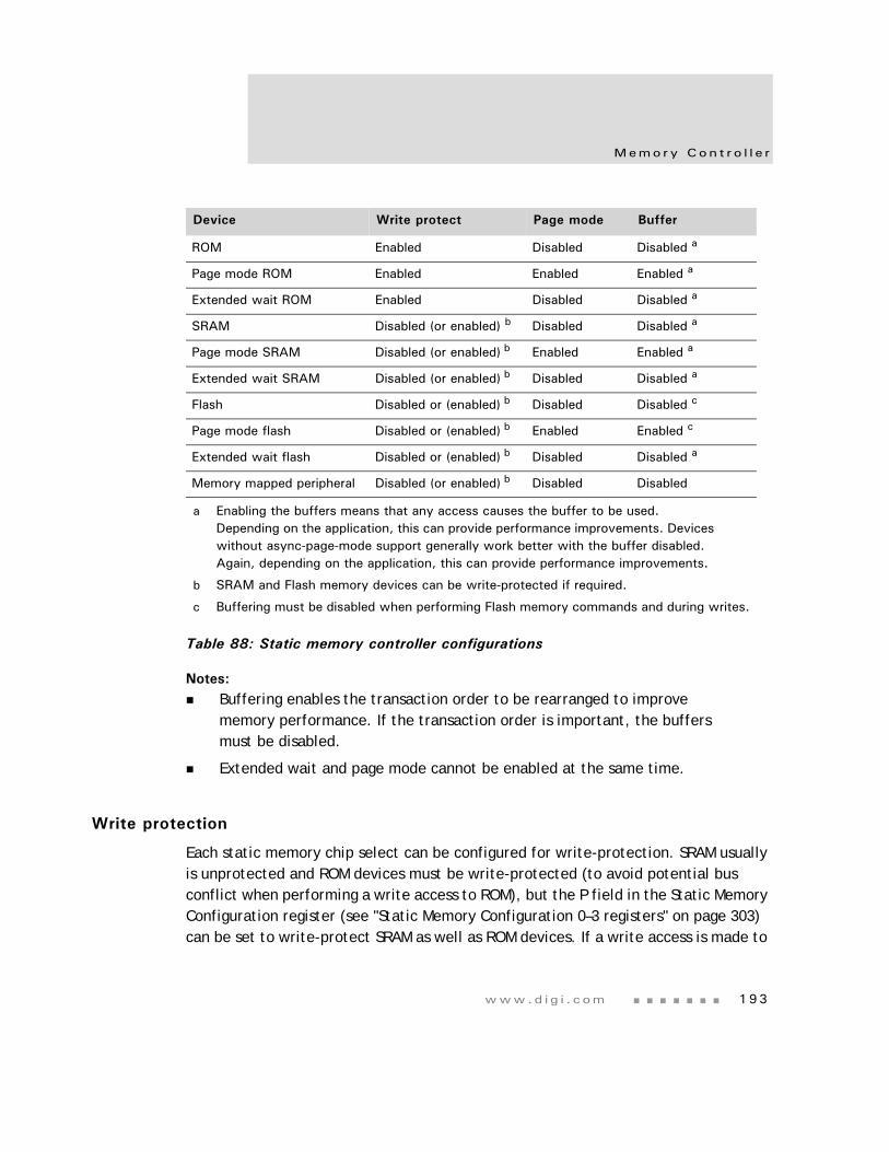
www.d i g i . com 193
Memo ry Con t r o l l e r
Notes:Buffering enables the transaction order to be rearranged to improve memory performance. If the transaction order is important, the buffers must be disabled.
Extended wait and page mode cannot be enabled at the same time.
Write protection
Each static memory chip select can be configured for write-protection. SRAM usually is unprotected and ROM devices must be write-protected (to avoid potential bus conflict when performing a write access to ROM), but the P field in the Static Memory Configuration register (see "Static Memory Configuration 0–3 registers" on page 303) can be set to write-protect SRAM as well as ROM devices. If a write access is made to
Device Write protect Page mode Buffer
ROM Enabled Disabled Disabled a
Page mode ROM Enabled Enabled Enabled a
Extended wait ROM Enabled Disabled Disabled a
SRAM Disabled (or enabled) b Disabled Disabled a
Page mode SRAM Disabled (or enabled) b Enabled Enabled a
Extended wait SRAM Disabled (or enabled) b Disabled Disabled a
Flash Disabled or (enabled) b Disabled Disabled c
Page mode flash Disabled or (enabled) b Enabled Enabled c
Extended wait flash Disabled or (enabled) b Disabled Disabled a
Memory mapped peripheral Disabled (or enabled) b Disabled Disabled
a Enabling the buffers means that any access causes the buffer to be used. Depending on the application, this can provide performance improvements. Devices without async-page-mode support generally work better with the buffer disabled. Again, depending on the application, this can provide performance improvements.
b SRAM and Flash memory devices can be write-protected if required.
c Buffering must be disabled when performing Flash memory commands and during writes.
Table 88: Static memory controller configurations
S t a t i c memo ry con t r o l l e r
1 9 4 NS9775 Ha r dwa r e Re f e r ence
a write-protected memory bank, an error is indicated by the HRESP[1:0] signal. If a write access is made to a memory bank containing ROM devices and the chip select is not write-protected. An error is not returned and the write access proceeds as normal. Note that this might lead to a bus conflict.
Extended wait transfers
The static memory controller supports extremely long transfer times. In normal use, the memory transfers are timed using the Static Memory Read Delay register (StaticWaitRd, see "Static Memory Read Delay 0–3 registers" on page 309) and Static Memory Wait Delay register (StaticWaitWr, see "Static Memory Write Delay 0–3 registers" on page 311). These registers allow transfers with up to 32 wait states. If a very slow static memory device has to be accessed, however, you can enable the static configuration extended wait (EW) bit. When EW is enabled, the Static Extended Wait register ("Static Memory Extended Wait register" on page 297) is used to time both the read and write transfers. The Static Extended Wait register allows transfers to have up to 16368 wait states.
Notes:Using extremely long transfer times might mean that SDRAM devices are not refreshed correctly.
Very slow transfers can degrade system performance, as the external memory interface is tied up for long periods of time. This has detrimental effects on time critical services, such as interrupt latency and low latency devices; for example, video controllers.
Memory mapped peripherals
Some systems use external peripherals that can be accessed using the static memory interface. Because of the way many of these peripherals function, the read and write transfers to them must not be buffered. The buffer must therefore be disabled.
Static memory initialization
Static memory must be initialized as required after poweron reset (reset_n) by programming the relevant registers in the memory controller as well as the configuration registers in the external static memory device.
www.d i g i . com 195
Memo ry Con t r o l l e r
Access sequencing and memory width
The data width of each external memory bank must be configured by programming the appropriate bank configuration register (Static Memory Configuration 0–3). When the external memory bus is narrower that the transfer initiated from the current main bus master, the internal bus transfer takes several external bus transfers to complete.
For example, if bank 0 is configured as 8-bit wide memory and a 32-bit read is initiated, the AHB bus stalls while the memory controller reads four consecutive bytes from the memory. During these accesses, the static memory controller block demultiplexes the four bytes into one 32-bit word on the AHB bus.
Wait state generation
Each bank of the memory controller must be configured for external transfer wait states in read and write accesses. Configure the banks by programming the appropriate bank control registers:
"Static Memory Configuration 0–3 registers" on page 303 (StaticConfig[n])
"Static Memory Write Enable Delay 0–3 registers" on page 307 (StaticWaitWen[n])
"Static Memory Output Enable Delay 0–3 registers" on page 308 (StaticWaitOen[n])
"Static Memory Read Delay 0–3 registers" on page 309 (StaticWaitRd[n])
"Static Memory Write Delay 0–3 registers" on page 311 (StaticWaitWr[n])
"Static Memory Page Mode Read Delay 0–3 registers" on page 310 (StaticWaitPage[n])
"Static Memory Turn Round Delay 0–3 registers" on page 312 (StaticWaitTurn[n])
"Static Memory Extended Wait register" on page 297 (StaticExtendedWait)
The number of cycles in which an AMBA transfer completes is controlled by two additional factors:
Access width
External memory width
S t a t i c memo ry con t r o l l e r
1 9 6 NS9775 Ha r dwa r e Re f e r ence
Each bank of the memory controller has a programmable enable for the extended wait (EW). The WAITRD wait state field in the Static Memory Read Delay register can be programmed to select from 1–32 wait states for read memory accesses to SRAM and ROM, or the initial read access to page mode devices. The WAITWR wait state field in the Static Memory Write Delay register can be programmed to select from 1–32 wait states for access to SRAM. The Static Memory Page Mode Read Delay register can be programmed to select from 1–32 wait states for page mode accesses.
Static memory read control
There are three types of static memory read controls:
Output enable programmable delay
ROM, SRAM, and flash
Asynchronous page mode read
Output enable programmable delayThe delay between the assertion of the chip select and the output enable is programmable from 0 to 15 cycles using the wait output enable bits (WAITOEN) in the Static Memory Output Enable Delay registers (see "Static Memory Output Enable Delay 0–3 registers" on page 308). The delay is used to reduce power consumption for memories that cannot provide valid output data immediately after the chip select has been asserted. The output enable is always deasserted at the same time as the chip select. at the end of the transfer.
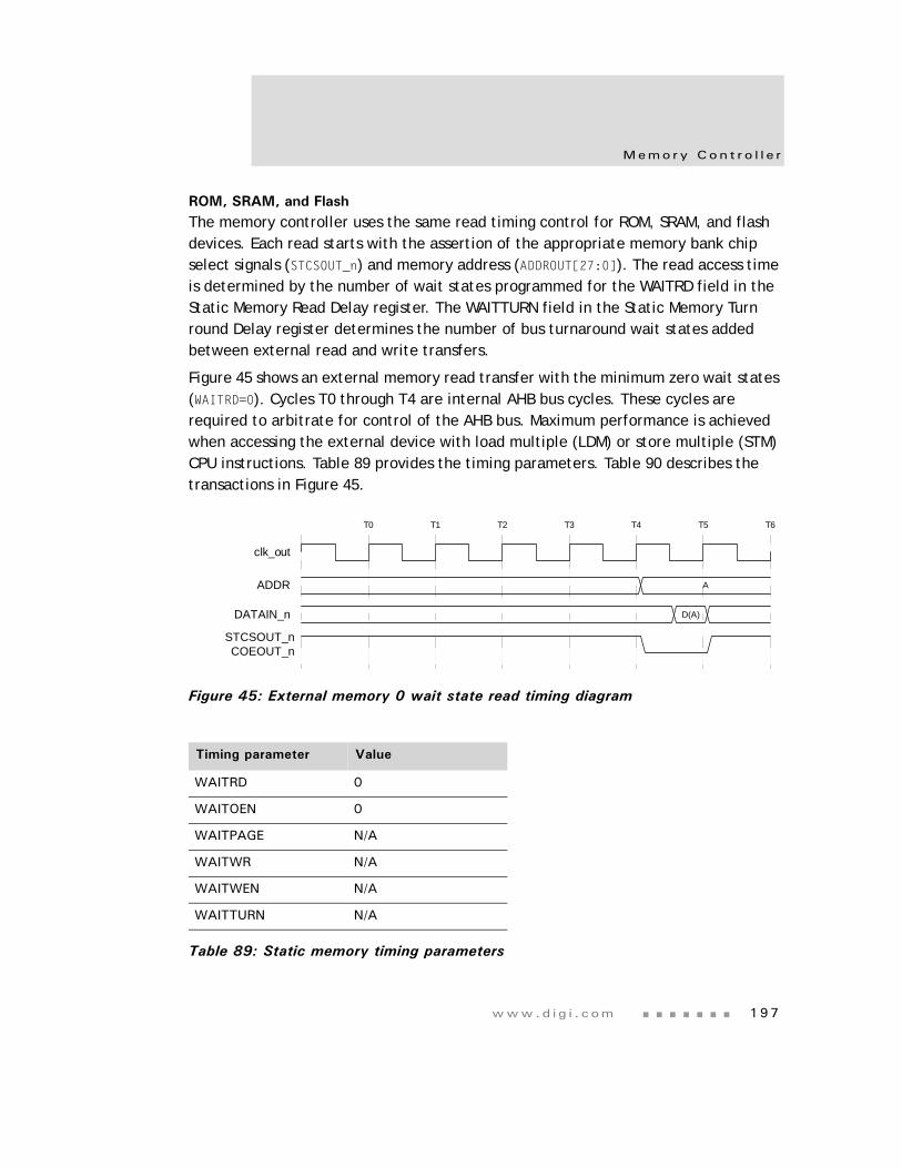
www.d i g i . com 197
Memo ry Con t r o l l e r
ROM, SRAM, and FlashThe memory controller uses the same read timing control for ROM, SRAM, and flash devices. Each read starts with the assertion of the appropriate memory bank chip select signals (STCSOUT_n) and memory address (ADDROUT[27:0]). The read access time is determined by the number of wait states programmed for the WAITRD field in the Static Memory Read Delay register. The WAITTURN field in the Static Memory Turn round Delay register determines the number of bus turnaround wait states added between external read and write transfers.
Figure 45 shows an external memory read transfer with the minimum zero wait states (WAITRD=0). Cycles T0 through T4 are internal AHB bus cycles. These cycles are required to arbitrate for control of the AHB bus. Maximum performance is achieved when accessing the external device with load multiple (LDM) or store multiple (STM) CPU instructions. Table 89 provides the timing parameters. Table 90 describes the transactions in Figure 45.
Figure 45: External memory 0 wait state read timing diagram
Timing parameter Value
WAITRD 0
WAITOEN 0
WAITPAGE N/A
WAITWR N/A
WAITWEN N/A
WAITTURN N/A
Table 89: Static memory timing parameters
clk_out
ADDR
DATAIN_n
STCSOUT_nCOEOUT_n
A
D(A)
T0 T1 T2 T3 T4 T5 T6
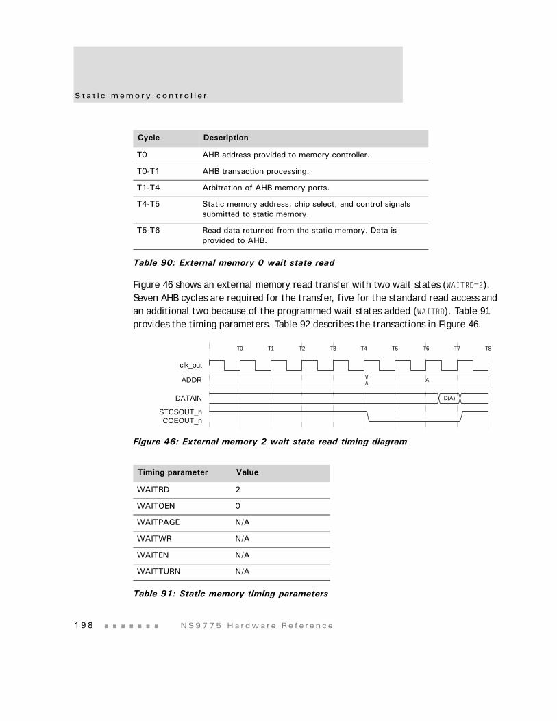
S t a t i c memo ry con t r o l l e r
1 9 8 NS9775 Ha r dwa r e Re f e r ence
Figure 46 shows an external memory read transfer with two wait states (WAITRD=2). Seven AHB cycles are required for the transfer, five for the standard read access and an additional two because of the programmed wait states added (WAITRD). Table 91 provides the timing parameters. Table 92 describes the transactions in Figure 46.
Figure 46: External memory 2 wait state read timing diagram
Cycle Description
T0 AHB address provided to memory controller.
T0-T1 AHB transaction processing.
T1-T4 Arbitration of AHB memory ports.
T4-T5 Static memory address, chip select, and control signals submitted to static memory.
T5-T6 Read data returned from the static memory. Data is provided to AHB.
Table 90: External memory 0 wait state read
Timing parameter Value
WAITRD 2
WAITOEN 0
WAITPAGE N/A
WAITWR N/A
WAITEN N/A
WAITTURN N/A
Table 91: Static memory timing parameters
STCSOUT_nCOEOUT_n
clk_out
ADDR
DATAIN
A
D(A)
T0 T1 T2 T3 T4 T5 T6 T7 T8
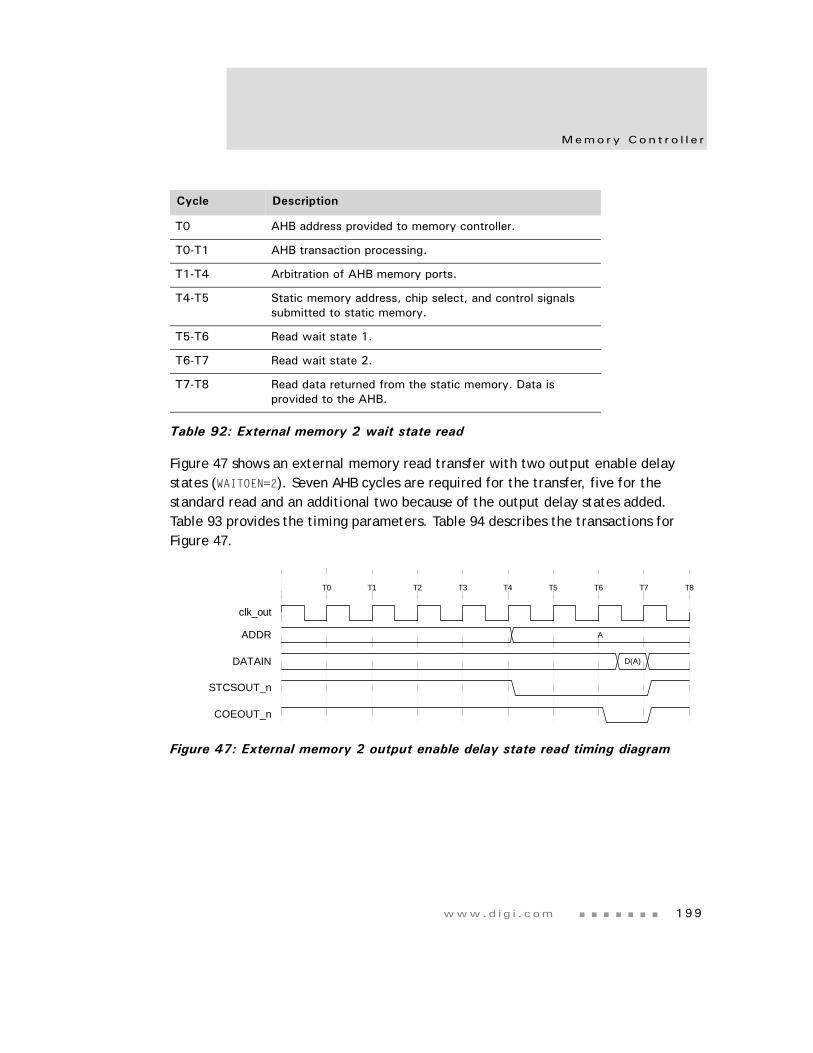
www.d i g i . com 199
Memo ry Con t r o l l e r
Figure 47 shows an external memory read transfer with two output enable delay states (WAITOEN=2). Seven AHB cycles are required for the transfer, five for the standard read and an additional two because of the output delay states added. Table 93 provides the timing parameters. Table 94 describes the transactions for Figure 47.
Figure 47: External memory 2 output enable delay state read timing diagram
Cycle Description
T0 AHB address provided to memory controller.
T0-T1 AHB transaction processing.
T1-T4 Arbitration of AHB memory ports.
T4-T5 Static memory address, chip select, and control signals submitted to static memory.
T5-T6 Read wait state 1.
T6-T7 Read wait state 2.
T7-T8 Read data returned from the static memory. Data is provided to the AHB.
Table 92: External memory 2 wait state read
ADDR
DATAIN
STCSOUT_n
A
D(A)
COEOUT_n
clk_out
T0 T1 T2 T3 T4 T5 T6 T7 T8
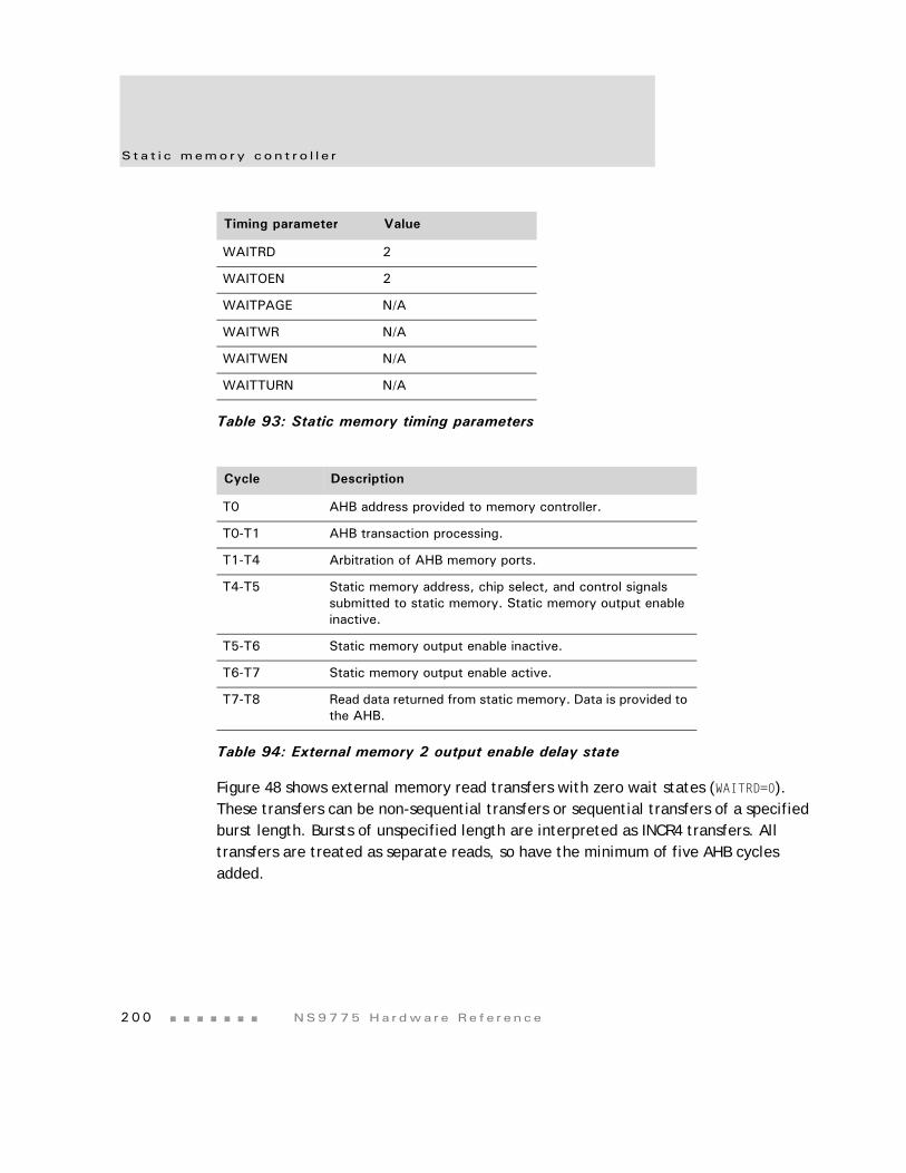
S t a t i c memo ry con t r o l l e r
2 0 0 NS9775 Ha r dwa r e Re f e r ence
Figure 48 shows external memory read transfers with zero wait states (WAITRD=0). These transfers can be non-sequential transfers or sequential transfers of a specified burst length. Bursts of unspecified length are interpreted as INCR4 transfers. All transfers are treated as separate reads, so have the minimum of five AHB cycles added.
Timing parameter Value
WAITRD 2
WAITOEN 2
WAITPAGE N/A
WAITWR N/A
WAITWEN N/A
WAITTURN N/A
Table 93: Static memory timing parameters
Cycle Description
T0 AHB address provided to memory controller.
T0-T1 AHB transaction processing.
T1-T4 Arbitration of AHB memory ports.
T4-T5 Static memory address, chip select, and control signals submitted to static memory. Static memory output enable inactive.
T5-T6 Static memory output enable inactive.
T6-T7 Static memory output enable active.
T7-T8 Read data returned from static memory. Data is provided to the AHB.
Table 94: External memory 2 output enable delay state
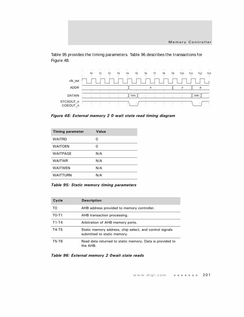
www.d i g i . com 201
Memo ry Con t r o l l e r
Table 95 provides the timing parameters. Table 96 describes the transactions for Figure 48.
Figure 48: External memory 2 0 wait state read timing diagram
Timing parameter Value
WAITRD 0
WAITOEN 0
WAITPAGE N/A
WAITWR N/A
WAITWEN N/A
WAITTURN N/A
Table 95: Static memory timing parameters
Cycle Description
T0 AHB address provided to memory controller.
T0-T1 AHB transaction processing.
T1-T4 Arbitration of AHB memory ports.
T4-T5 Static memory address, chip select, and control signals submitted to static memory.
T5-T6 Read data returned to static memory. Data is provided to the AHB.
Table 96: External memory 2 0wait state reads
ADDR
DATAIN
STCSOUT_nCOEOUT_n
B
D(B)
A 0
D(A)
clk_out
T0 T1 T2 T3 T4 T5 T6 T7 T8 T9 T10 T11 T12 T13
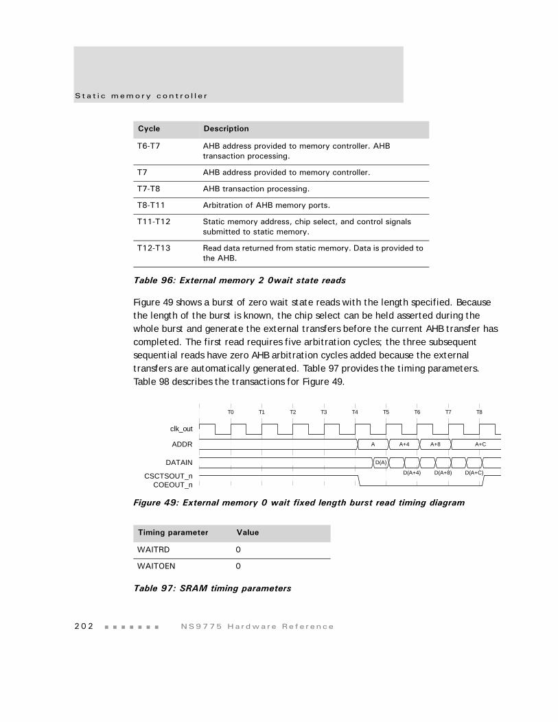
S t a t i c memo ry con t r o l l e r
2 0 2 NS9775 Ha r dwa r e Re f e r ence
Figure 49 shows a burst of zero wait state reads with the length specified. Because the length of the burst is known, the chip select can be held asserted during the whole burst and generate the external transfers before the current AHB transfer has completed. The first read requires five arbitration cycles; the three subsequent sequential reads have zero AHB arbitration cycles added because the external transfers are automatically generated. Table 97 provides the timing parameters. Table 98 describes the transactions for Figure 49.
Figure 49: External memory 0 wait fixed length burst read timing diagram
T6-T7 AHB address provided to memory controller. AHB transaction processing.
T7 AHB address provided to memory controller.
T7-T8 AHB transaction processing.
T8-T11 Arbitration of AHB memory ports.
T11-T12 Static memory address, chip select, and control signals submitted to static memory.
T12-T13 Read data returned from static memory. Data is provided to the AHB.
Timing parameter Value
WAITRD 0
WAITOEN 0
Table 97: SRAM timing parameters
Cycle Description
Table 96: External memory 2 0wait state reads
ADDR
DATAIN
A+C
CSCTSOUT_nCOEOUT_n
A A+4 A+8
D(A)
D(A+4) D(A+8) D(A+C)
clk_out
T0 T1 T2 T3 T4 T5 T6 T7 T8
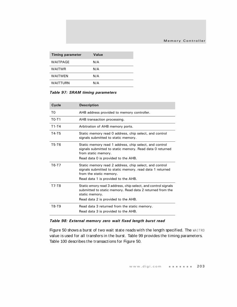
www.d i g i . com 203
Memo ry Con t r o l l e r
Figure 50 shows a burst of two wait state reads with the length specified. The WAITRD value is used for all transfers in the burst. Table 99 provides the timing parameters. Table 100 describes the transactions for Figure 50.
WAITPAGE N/A
WAITWR N/A
WAITWEN N/A
WAITTURN N/A
Cycle Description
T0 AHB address provided to memory controller.
T0-T1 AHB transaction processing.
T1-T4 Arbitration of AHB memory ports.
T4-T5 Static memory read 0 address, chip select, and control signals submitted to static memory.
T5-T6 Static memory read 1 address, chip select, and control signals submitted to static memory. Read data 0 returned from static memory. Read data 0 is provided to the AHB.
T6-T7 Static memory read 2 address, chip select, and control signals submitted to static memory. read data 1 returned from the static memory. Read data 1 is provided to the AHB.
T7-T8 Static emory read 3 address, chip select, and control signals submitted to static memory. Read data 2 returned from the static memory.Read data 2 is provided to the AHB.
T8-T9 Read data 3 returned from the static memory. Read data 3 is provided to the AHB.
Table 98: External memory zero wait fixed length burst read
Timing parameter Value
Table 97: SRAM timing parameters
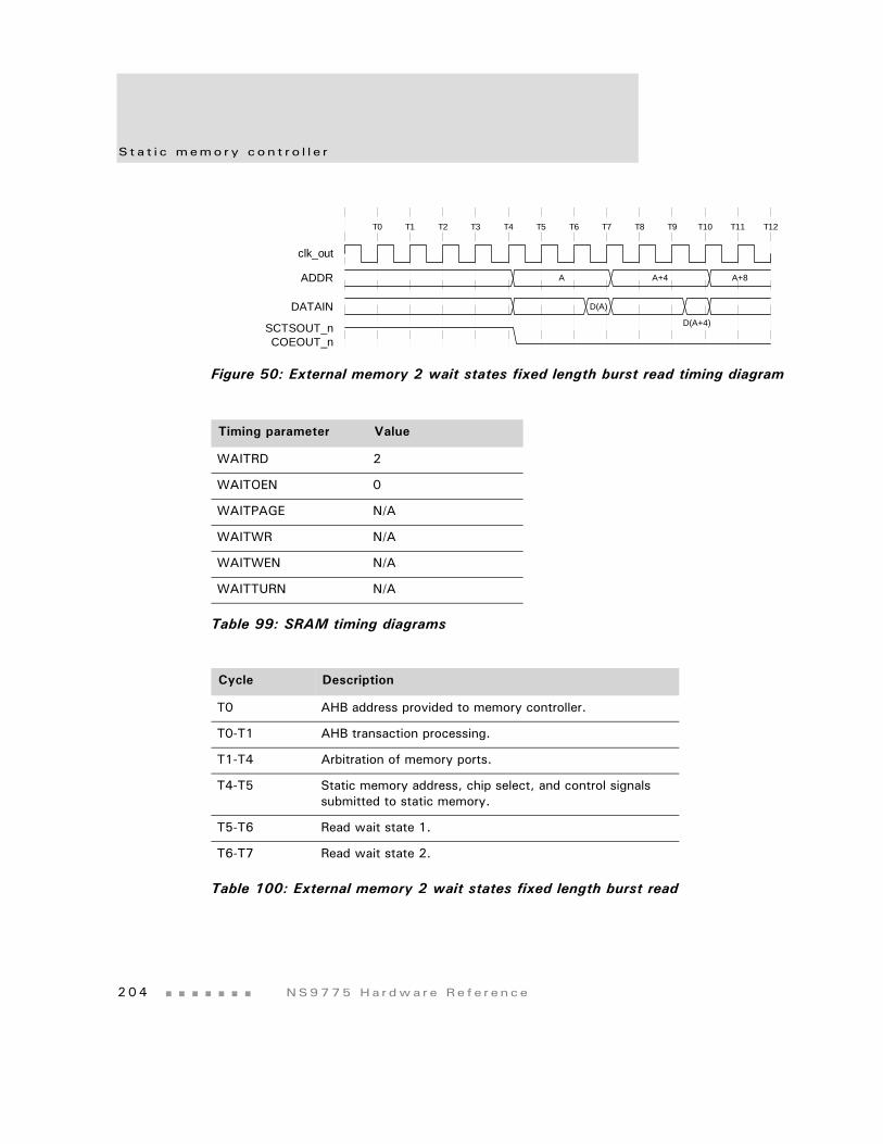
S t a t i c memo ry con t r o l l e r
2 0 4 NS9775 Ha r dwa r e Re f e r ence
Figure 50: External memory 2 wait states fixed length burst read timing diagram
Timing parameter Value
WAITRD 2
WAITOEN 0
WAITPAGE N/A
WAITWR N/A
WAITWEN N/A
WAITTURN N/A
Table 99: SRAM timing diagrams
Cycle Description
T0 AHB address provided to memory controller.
T0-T1 AHB transaction processing.
T1-T4 Arbitration of memory ports.
T4-T5 Static memory address, chip select, and control signals submitted to static memory.
T5-T6 Read wait state 1.
T6-T7 Read wait state 2.
Table 100: External memory 2 wait states fixed length burst read
ADDR
DATAIN
A+8
SCTSOUT_nCOEOUT_n
A A+4
D(A)
D(A+4)
clk_out
T0 T1 T2 T3 T4 T5 T6 T7 T12T10 T11T8 T9
www.d i g i . com 205
Memo ry Con t r o l l e r
Asynchronous page mode readThe memory controller supports asynchronous page mode read of up to four memory transfers by updating address bits A[1] and A[0]. This feature increases the bandwidth by using a reduced access time for the read accesses that are in page mode. The first read access takes static wait read and WAITRD cycles. Subsequent read accesses that are in page mode take static wait page and WAITPAGE cycles. The chip select and output enable lines are held during the burst, and only the lower two address bits change between subsequent accesses. At the end of the burst, the chip select and output enable lines are deasserted together.
Figure 51 shows an external memory page mode read transfer with two initial wait states and one sequential wait state. The first read requires five AHB arbitration cycles (plus three wait states); the following (up to 3) sequential transfers have only one AHB wait state. This gives increased performance over the equivalent nonpage mode ROM timing (see Figure 50, "External memory 2 wait states fixed length burst read timing diagram," on page 204). Table 101 provides the timing parameters. Table 102 describes the transactions for Figure 51.
T7-T8 Read data 0 returned from the static memory. Read data 0 is provided to the AHB. Static memory transfer 1, address, chip select, and control signals submitted to static memory.
T8-T9 Read wait state 1.
T9-T10 Read wait state 2.
T10-T11 Read data 1 returned from the static memory. Read data 1 is provided to the AHB. Static memory transfer 2, address, chip select, and control signals submitted to static memory.
T11-T12 Read wait state 1.
Cycle Description
Table 100: External memory 2 wait states fixed length burst read
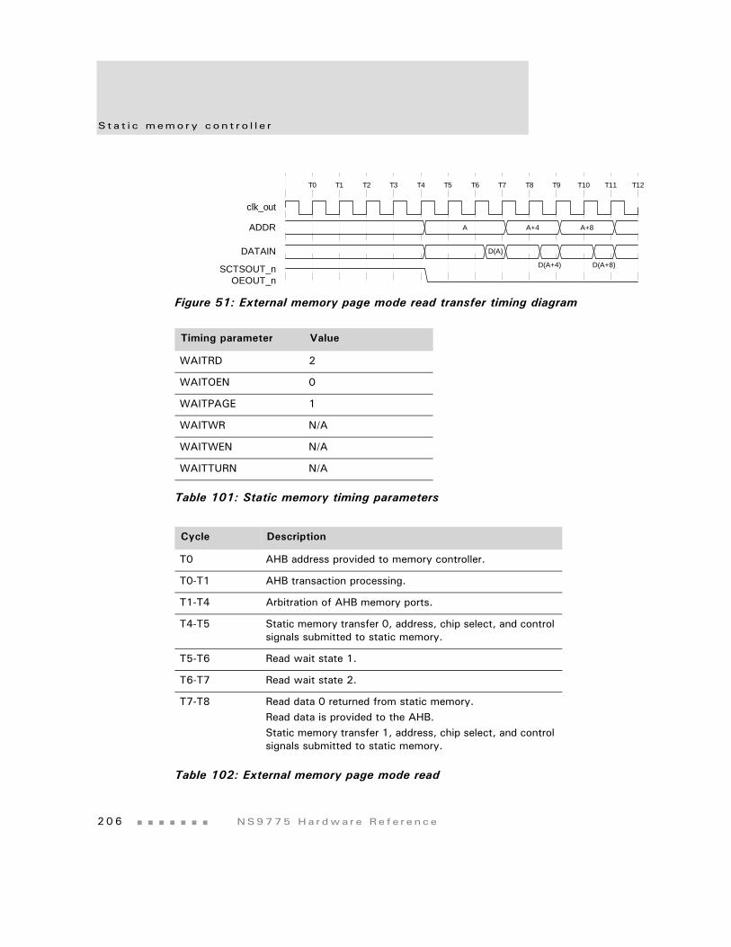
S t a t i c memo ry con t r o l l e r
2 0 6 NS9775 Ha r dwa r e Re f e r ence
Figure 51: External memory page mode read transfer timing diagram
Timing parameter Value
WAITRD 2
WAITOEN 0
WAITPAGE 1
WAITWR N/A
WAITWEN N/A
WAITTURN N/A
Table 101: Static memory timing parameters
Cycle Description
T0 AHB address provided to memory controller.
T0-T1 AHB transaction processing.
T1-T4 Arbitration of AHB memory ports.
T4-T5 Static memory transfer 0, address, chip select, and control signals submitted to static memory.
T5-T6 Read wait state 1.
T6-T7 Read wait state 2.
T7-T8 Read data 0 returned from static memory. Read data is provided to the AHB. Static memory transfer 1, address, chip select, and control signals submitted to static memory.
Table 102: External memory page mode read
ADDR
DATAIN
SCTSOUT_nOEOUT_n
A A+4
D(A)
D(A+4) D(A+8)
A+8
clk_out
T0 T1 T2 T3 T4 T5 T6 T7 T12T10 T11T8 T9
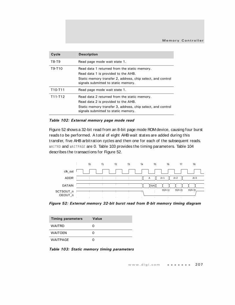
www.d i g i . com 207
Memo ry Con t r o l l e r
Figure 52 shows a 32-bit read from an 8-bit page mode ROM device, causing four burst reads to be performed. A total of eight AHB wait states are added during this transfer, five AHB arbitration cycles and then one for each of the subsequent reads. WAITRD and WAITPAGE are 0. Table 103 provides the timing parameters. Table 104 describes the transactions for Figure 52.
Figure 52: External memory 32-bit burst read from 8-bit memory timing diagram
T8-T9 Read page mode wait state 1.
T9-T10 Read data 1 returned from the static memory. Read data 1 is provided to the AHB. Static memory transfer 2, address, chip select, and control signals submitted to static memory.
T10-T11 Read page mode wait state 1.
T11-T12 Read data 2 returned from the static memory. Read data 2 is provided to the AHB. Static memory transfer 3, address, chip select, and control signals submitted to static memory.
Timing parameters Value
WAITRD 0
WAITOEN 0
WAITPAGE 0
Table 103: Static memory timing parameters
Cycle Description
Table 102: External memory page mode read
ADDR
DATAIN
A+3
SCTSOUT_nOEOUT_n
A A+1 A+2
D(A)
D(A+1) D(A+2) D(A+3)
clk_out
T0 T1 T2 T3 T4 T5 T6 T7 T8
S t a t i c memo ry con t r o l l e r
2 0 8 NS9775 Ha r dwa r e Re f e r ence
Static memory write control
Write enable programming delayThe delay between the assertion of the chip select and the write enable is programmable from 0 to 15 cycles using the WAITWEN bits of the Static Memory Write Enable Delay (StaticWaitWen[3:0]) registers. The delay reduces the power consumption for memories. The write enable is asserted on the rising edge of HCLK after the assertion of the chip select for zero wait states. The write enable is always
WAITWR N/A
WAITWEN N/A
WAITTURN N/A
Cycle Description
T0 AHB address provided to memory controller.
T0-T1 AHB transaction processing.
T1-T4 Arbitration of AHB memory ports.
T4-T5 Static memory transfer m0, address, chip select, and control signals submitted to static memory.
T5-T6 Static memory transfer 1, address, chip select, and control signals submitted to static memory. Read data byte 0 returned from static memory.
T6-T7 Static memory transfer 2, address, chip select, and control signals submitted to static memory. Read data byte 1 returned from the static memory.
T7-T8 Static memory transfer 3, address chip select, and control signals submitted to static memory. Read data byte 2 returned from the static memory.
T8-T9 Read data byte 3 returned from the static memory. Read data 32-bit word is provided to the AHB.
Table 104: External memory 32-bit burst read from 8-bit memory
Timing parameters Value
Table 103: Static memory timing parameters
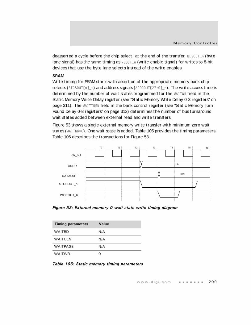
www.d i g i . com 209
Memo ry Con t r o l l e r
deasserted a cycle before the chip select, at the end of the transfer. BLSOUT_n (byte lane signal) has the same timing as WEOUT_n (write enable signal) for writes to 8-bit devices that use the byte lane selects instead of the write enables.
SRAMWrite timing for SRAM starts with assertion of the appropriate memory bank chip selects (STCSOUT[n]_n) and address signals (ADDROUT[27:0]_n). The write access time is determined by the number of wait states programmed for the WAITWR field in the Static Memory Write Delay register (see "Static Memory Write Delay 0–3 registers" on page 311). The WAITTURN field in the bank control register (see "Static Memory Turn Round Delay 0–3 registers" on page 312) determines the number of bus turnaround wait states added between external read and write transfers.
Figure 53 shows a single external memory write transfer with minimum zero wait states (WAITWR=0). One wait state is added. Table 105 provides the timing parameters. Table 106 describes the transactions for Figure 53.
Figure 53: External memory 0 wait state write timing diagram
Timing parameters Value
WAITRD N/A
WAITOEN N/A
WAITPAGE N/A
WAITWR 0
Table 105: Static memory timing parameters
ADDR
DATAOUT
STCSOUT_n
WOEOUT_n
A
D(A)
clk_out
T0 T1 T2 T3 T4 T5 T6
S t a t i c memo ry con t r o l l e r
2 1 0 NS9775 Ha r dwa r e Re f e r ence
Figure 54 shows a single external memory write transfer with two wait states (WAITWR=2). One AHB wait state is added. Table 107 provides the timing parameters. Table 108 describes the transactions for Figure 54.
WAITWEN 0
WAITTURN N/A
Cycle Description
T0 AHB address provided to memory controller.
T0-T1 AHB transaction processing.
T1-T4 Arbitration of AHB memory ports.
T4-T5 Static memory transfer 0, address, chip select, and control signals submitted to static memory.Write data is read from the AHB memory port.Write enable inactive.
T5-T6 Write enable taken active.Write data submitted to static memory.Static memory writes the data.
T6-T7 Static memory writes the data.Write enable taken inactive.
T7-T8 Static memory control signals taken inactive.
Table 106: External memory 0 wait state write
Timing parameters Value
Table 105: Static memory timing parameters
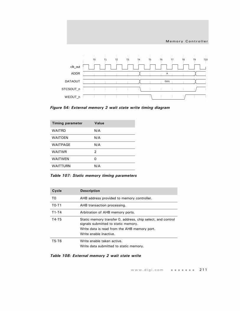
www.d i g i . com 211
Memo ry Con t r o l l e r
Figure 54: External memory 2 wait state write timing diagram
Timing parameter Value
WAITRD N/A
WAITOEN N/A
WAITPAGE N/A
WAITWR 2
WAITWEN 0
WAITTURN N/A
Table 107: Static memory timing parameters
Cycle Description
T0 AHB address provided to memory controller.
T0-T1 AHB transaction processing.
T1-T4 Arbitration of AHB memory ports.
T4-T5 Static memory transfer 0, address, chip select, and control signals submitted to static memory.Write data is read from the AHB memory port.Write enable inactive.
T5-T6 Write enable taken active.Write data submitted to static memory.
Table 108: External memory 2 wait state write
ADDR
DATAOUT
A
STCSOUT_n
D(A)
WEOUT_n
clk_out
T0 T1 T2 T3 T4 T5 T6 T7 T8 T9 T10
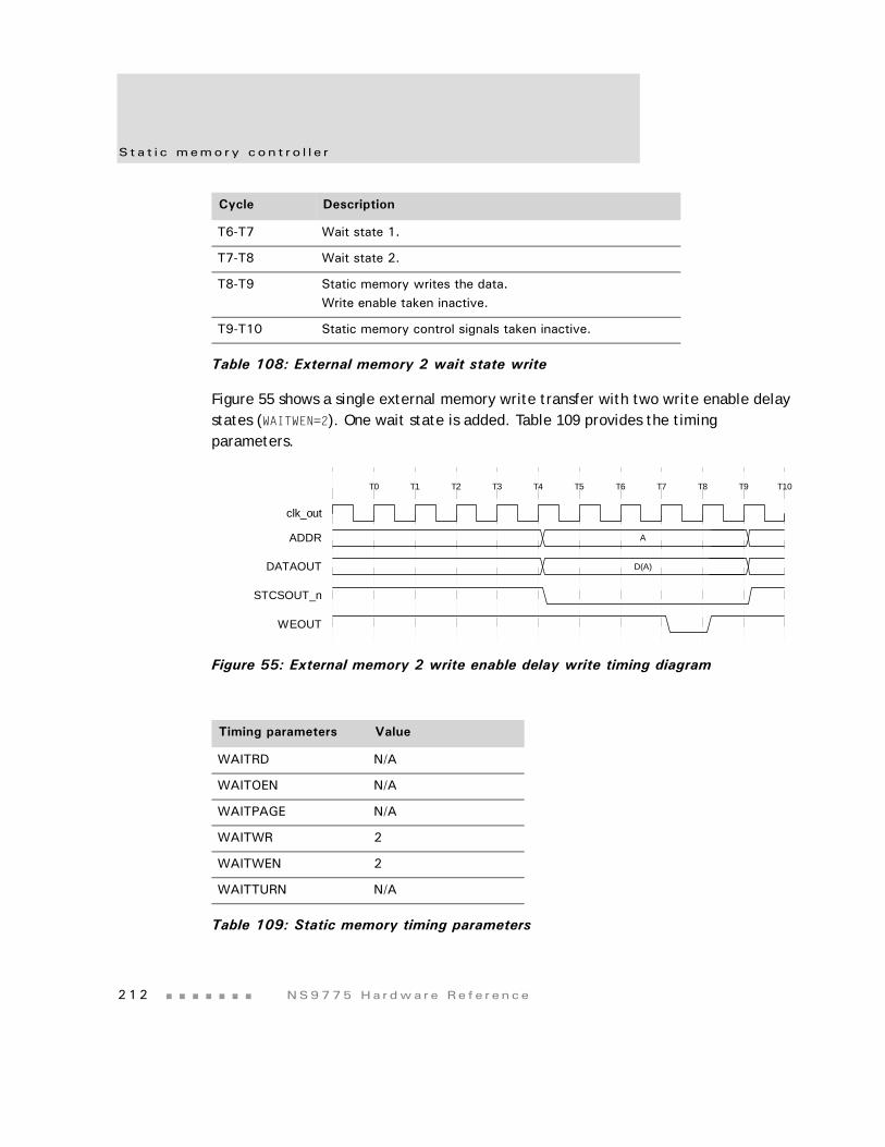
S t a t i c memo ry con t r o l l e r
2 1 2 NS9775 Ha r dwa r e Re f e r ence
Figure 55 shows a single external memory write transfer with two write enable delay states (WAITWEN=2). One wait state is added. Table 109 provides the timing parameters.
Figure 55: External memory 2 write enable delay write timing diagram
T6-T7 Wait state 1.
T7-T8 Wait state 2.
T8-T9 Static memory writes the data.Write enable taken inactive.
T9-T10 Static memory control signals taken inactive.
Timing parameters Value
WAITRD N/A
WAITOEN N/A
WAITPAGE N/A
WAITWR 2
WAITWEN 2
WAITTURN N/A
Table 109: Static memory timing parameters
Cycle Description
Table 108: External memory 2 wait state write
ADDR
DATAOUT
A
STCSOUT_n
D(A)
WEOUT
clk_out
T0 T1 T2 T3 T4 T5 T6 T7 T8 T9 T10
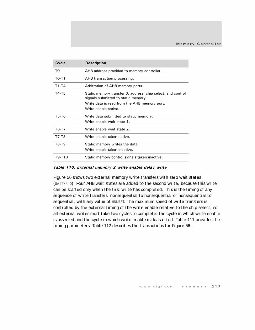
www.d i g i . com 213
Memo ry Con t r o l l e r
Figure 56 shows two external memory write transfers with zero wait states (WAITWR=0). Four AHB wait states are added to the second write, because this write can be started only when the first write has completed. This is the timing of any sequence of write transfers, nonsequential to nonsequential or nonsequential to sequential, with any value of HBURST. The maximum speed of write transfers is controlled by the external timing of the write enable relative to the chip select, so all external writes must take two cycles to complete: the cycle in which write enable is asserted and the cycle in which write enable is deasserted. Table 111 provides the timing parameters. Table 112 describes the transactions for Figure 56.
Cycle Description
T0 AHB address provided to memory controller.
T0-T1 AHB transaction processing.
T1-T4 Arbitration of AHB memory ports.
T4-T5 Static memory transfer 0, address, chip select, and control signals submitted to static memory.Write data is read from the AHB memory port.Write enable active.
T5-T6 Write data submitted to static memory.Write enable wait state 1.
T6-T7 Write enable wait state 2.
T7-T8 Write enable taken active.
T8-T9 Static memory writes the data.Write enable taken inactive.
T9-T10 Static memory control signals taken inactive.
Table 110: External memory 2 write enable delay write
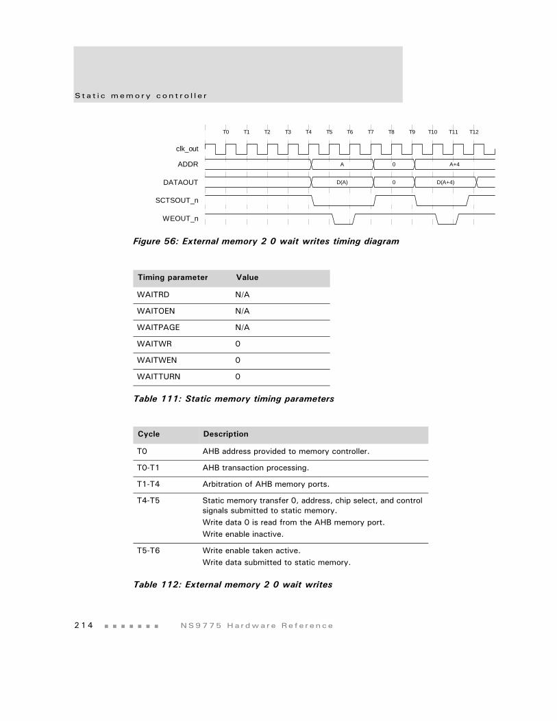
S t a t i c memo ry con t r o l l e r
2 1 4 NS9775 Ha r dwa r e Re f e r ence
Figure 56: External memory 2 0 wait writes timing diagram
Timing parameter Value
WAITRD N/A
WAITOEN N/A
WAITPAGE N/A
WAITWR 0
WAITWEN 0
WAITTURN 0
Table 111: Static memory timing parameters
Cycle Description
T0 AHB address provided to memory controller.
T0-T1 AHB transaction processing.
T1-T4 Arbitration of AHB memory ports.
T4-T5 Static memory transfer 0, address, chip select, and control signals submitted to static memory.Write data 0 is read from the AHB memory port.Write enable inactive.
T5-T6 Write enable taken active.Write data submitted to static memory.
Table 112: External memory 2 0 wait writes
ADDR
DATAOUT
A+4
SCTSOUT_n
A 0
D(A) 0
WEOUT_n
D(A+4)
clk_out
T0 T1 T2 T3 T4 T5 T6 T7 T10 T11T8 T9 T12
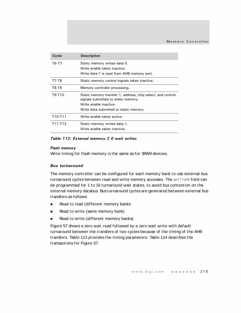
www.d i g i . com 215
Memo ry Con t r o l l e r
Flash memoryWrite timing for flash memory is the same as for SRAM devices.
Bus turnaround
The memory controller can be configured for each memory bank to use external bus turnaround cycles between read and write memory accesses. The WAITTURN field can be programmed for 1 to 16 turnaround wait states, to avoid bus contention on the external memory databus. Bus turnaround cycles are generated between external bus transfers as follows:
Read to read (different memory banks
Read to write (same memory bank)
Read to write (different memory banks)
Figure 57 shows a zero wait read followed by a zero wait write with default turnaround between the transfers of two cycles because of the timing of the AHB transfers. Table 113 provides the timing parameters. Table 114 describes the transactions for Figure 57.
T6-T7 Static memory writes data 0.Write enable taken inactive.Write data 1 is read from AHB memory port.
T7-T8 Static memory control signals taken inactive.
T8-T9 Memory controller processing.
T9-T10 Static memory transfer 1, address, chip select, and control signals submitted to static memory.Write enable inactive.Write data submitted to static memory.
T10-T11 Write enable taken active.
T11-T12 Static memory writes data 1.Write enable taken inactive.
Cycle Description
Table 112: External memory 2 0 wait writes
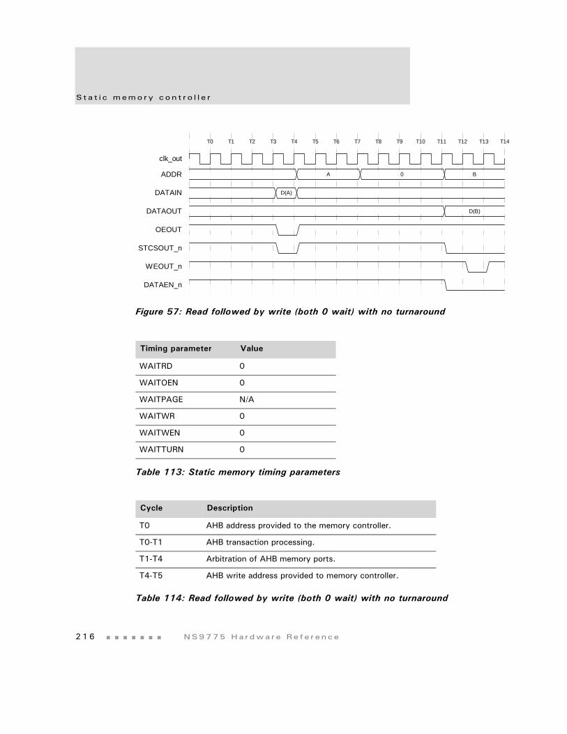
S t a t i c memo ry con t r o l l e r
2 1 6 NS9775 Ha r dwa r e Re f e r ence
Figure 57: Read followed by write (both 0 wait) with no turnaround
Timing parameter Value
WAITRD 0
WAITOEN 0
WAITPAGE N/A
WAITWR 0
WAITWEN 0
WAITTURN 0
Table 113: Static memory timing parameters
Cycle Description
T0 AHB address provided to the memory controller.
T0-T1 AHB transaction processing.
T1-T4 Arbitration of AHB memory ports.
T4-T5 AHB write address provided to memory controller.
Table 114: Read followed by write (both 0 wait) with no turnaround
ADDR
DATAIN
B
OEOUT
A 0
D(A)
STCSOUT_n
DATAOUT D(B)
WEOUT_n
DATAEN_n
clk_out
T0 T1 T2 T3 T4 T5 T6 T7 T10 T11T8 T9 T12 T13 T14
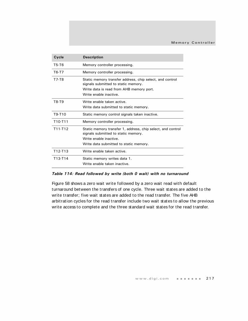
www.d i g i . com 217
Memo ry Con t r o l l e r
Figure 58 shows a zero wait write followed by a zero wait read with default turnaround between the transfers of one cycle. Three wait states are added to the write transfer; five wait states are added to the read transfer. The five AHB arbitration cycles for the read transfer include two wait states to allow the previous write access to complete and the three standard wait states for the read transfer.
T5-T6 Memory controller processing.
T6-T7 Memory controller processing.
T7-T8 Static memory transfer address, chip select, and control signals submitted to static memory.Write data is read from AHB memory port.Write enable inactive.
T8-T9 Write enable taken active.Write data submitted to static memory.
T9-T10 Static memory control signals taken inactive.
T10-T11 Memory controller processing.
T11-T12 Static memory transfer 1, address, chip select, and control signals submitted to static memory.Write enable inactive.Write data submitted to static memory.
T12-T13 Write enable taken active.
T13-T14 Static memory writes data 1.Write enable taken inactive.
Cycle Description
Table 114: Read followed by write (both 0 wait) with no turnaround
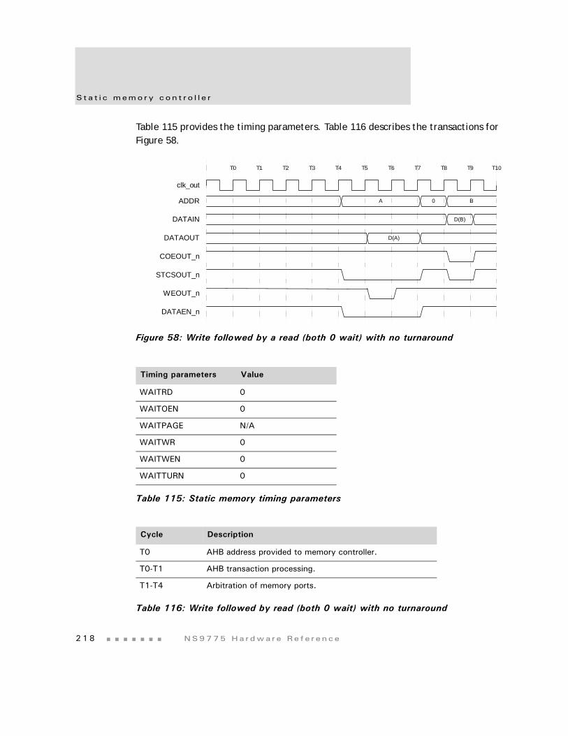
S t a t i c memo ry con t r o l l e r
2 1 8 NS9775 Ha r dwa r e Re f e r ence
Table 115 provides the timing parameters. Table 116 describes the transactions for Figure 58.
Figure 58: Write followed by a read (both 0 wait) with no turnaround
Timing parameters Value
WAITRD 0
WAITOEN 0
WAITPAGE N/A
WAITWR 0
WAITWEN 0
WAITTURN 0
Table 115: Static memory timing parameters
Cycle Description
T0 AHB address provided to memory controller.
T0-T1 AHB transaction processing.
T1-T4 Arbitration of memory ports.
Table 116: Write followed by read (both 0 wait) with no turnaround
ADDR
DATAIN
B
STCSOUT_n
WEOUT_n
DATAOUT
COEOUT_n
DATAEN_n
0A
D(B)
D(A)
clk_out
T0 T1 T2 T3 T4 T5 T6 T7 T8 T9 T10
www.d i g i . com 219
Memo ry Con t r o l l e r
Figure 59 shows a zero wait read followed by a zero wait write with two turnaround cycles added. The standard minimum of three AHB arbitration cycles are added to the read transfer and two wait states are added to the write transfer (as for any read-write transfer sequence).
T4-T5 Static memory address, chip select, and control signals submitted to static memory.Write data is read from AHB memory port.Write enable inactive.AHB read address provided to memory controller.
T5-T6 Write enable taken active.Write data submitted to static memory.
T6-T7 Static memory writes the data.Write enable taken inactive.
T7-T8 Static memory control signals taken inactive.
T8-T9 Static memory address, chip select, and control signals submitted to static memory.
T9-T10 Read data returned from the static memory. Data is provided to the AHB.
Cycle Description
Table 116: Write followed by read (both 0 wait) with no turnaround
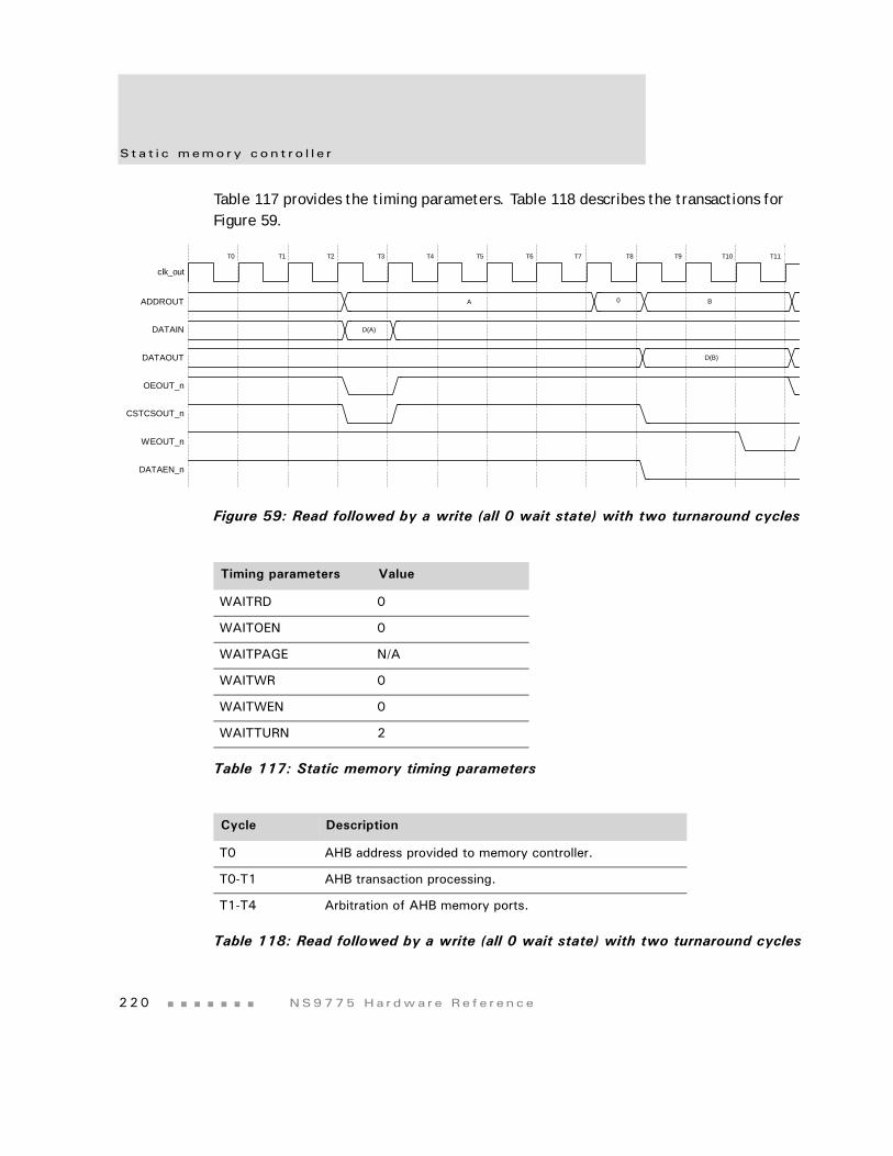
S t a t i c memo ry con t r o l l e r
2 2 0 NS9775 Ha r dwa r e Re f e r ence
Table 117 provides the timing parameters. Table 118 describes the transactions for Figure 59.
Figure 59: Read followed by a write (all 0 wait state) with two turnaround cycles
ADDROUT
DATAIN
OEOUT_n
D(A)
DATAOUT D(B)
WEOUT_n
DATAEN_n
CSTCSOUT_n
BA 0
clk_out
T0 T1 T2 T3 T4 T5 T6 T7 T8 T9 T10 T11
Timing parameters Value
WAITRD 0
WAITOEN 0
WAITPAGE N/A
WAITWR 0
WAITWEN 0
WAITTURN 2
Table 117: Static memory timing parameters
Cycle Description
T0 AHB address provided to memory controller.
T0-T1 AHB transaction processing.
T1-T4 Arbitration of AHB memory ports.
Table 118: Read followed by a write (all 0 wait state) with two turnaround cycles
www.d i g i . com 221
Memo ry Con t r o l l e r
Byte lane control
The memory controller generates the byte lane control signals BLSOUT[3:0]_n according to these attributes:
Little or big endian operation
AMBA transfer width, indicated by HSIZE[2:0]
External memory bank databus width, defined within each control register
The decoded HADDR[1:0] value for write accesses only
Word transfers are the largest size transfers supported by the memory controller. Any access tried with a size greater that a word causes an error response. Each memory chip select can be 8, 16, or 32 bits wide. The memory type used determines how the WEOUT_n and BLSOUT_n signals are connected to provide byte, halfword, and word access.
For read accesses, you must control the BLSOUT_n signals by driving them all high or all low. Do this by programming the byte lane state (PB) bit in the Static
T4-T5 Static memory address, chip select, and control signals submitted to static memory.
T5-T6 Read data returned from static memory. Data is provided to the AHB.AHB write address provided to memory controller.
T6-T7 Turn around cycle 1.
T7-T8 Turn around cycle 2.
T8-T9 Static memory transfer address, chip select, and control signals submitted to static memory.Write enable inactive.
T9-T10 Memory controller processing.
T10-T11 Write enable taken active. Write data submitted to static memory.
T11-T12 Static memory writes the data.Write enable taken inactive.
Cycle Description
Table 118: Read followed by a write (all 0 wait state) with two turnaround cycles
S t a t i c memo ry con t r o l l e r
2 2 2 NS9775 Ha r dwa r e Re f e r ence
Configuration [3:0] register. "Memory banks constructed from 8-bit or non-byte-partitioned memory devices" on page 222 and "Memory banks constructed from 8-bit or non-byte-partitioned memory devices" on page 222 explain why different connections, with respect to WEOUT_n and BLSOUT[3:0]_n, for different memory configurations.
Address connectivity
The static memory address output signal ADDROUT[27:0] must be right-justified.
Memory banks constructed from 8-bit or non-byte-partitioned memory devices
For memory banks constructed from 8-bit or non-byte-partitioned memory devices, it is important that the byte lane state (PB) bit is cleared to 0 within the respective memory bank control register. This forces all BLSOUT[3:0]_n lines high during a read access, as the byte lane selects are connected to the device write enables.
www.d i g i . com 223
Memo ry Con t r o l l e r
Figure 60: Memory banks constructed from 8-bit memory
Figure 60 shows 8-bit memory configuring memory banks that are 8-, 16-, and 32-bits wide. In each of these configurations, the BLSOUT[3:0]_n signals are connected to write enable (WE_n) inputs of each 8-bit memory. The WEOUT signal from the memory controller is not used.
For write transfers, the appropriate BLSOUT[3:0]_n byte lane signals are asserted low, and direct the data to the addressed bytes.
For read transfers, all BLSOUT[3:0]_n signals are deasserted high, enabling the external bus to be defined for at least the width of the accessed memory.
A[20:0]
CE_n
OE_n
WE_n
IO[7:0]
BLSOUT[3]_n
DATA[31:24]
A[20:0]
CE_n
OE_n
WE_n
IO[7:0]
BLSOUT[2]_n
DATA[23:16]
A[20:0]
CE_n
OE_n
WE_n
IO[7:0]
BLSOUT[1]_n
DATA[15:8]
A[20:0]
CE_n
OE_n
WE_n
IO[7:0]
BLSOUT[0]_n
DATA[7:0]
32-bit bank consisting of four 8-bit devices
A[20:0]
CE_n
OE_n
WE_n
IO[7:0]
BLSOUT[1]_n
DATA[15:8]
A[20:0]
CE_n
OE_n
WE_n
IO[7:0]
BLSOUT[0]_n
DATA[7:0]
16-bit bank consisting of two 8-bit devices
A[20:0]
CE_n
OE_n
WE_n
IO[7:0]
BLSOUT[0]_n
DATA[7:0]
OEOUT_n
ADDROUT[20:0]_n
STCSOUT_n
8-bit bank consisting of one 8-bit device
ADDROUT[20:0]
STCSOUT_n
OEOUT_n
ADDROUT[20:0]
STCSOUT_n
OEOUT_n
S t a t i c memo ry con t r o l l e r
2 2 4 NS9775 Ha r dwa r e Re f e r ence
Memory banks constructed from 16-or 32-bit memory devices
For memory banks constructed from 16- or 32-bit memory devices, it is important that the byte lane select (PB) bit is set to 1 within the respective memory bank control register. This asserts all BLSOUT[3:0]_n lines low during a read access as, during a read, all device bytes must be selected to avoid undriven byte lanes on the read data value. With 16- and 32-bit wide memory devices, byte select signals exist and must be appropriately controlled; see Figure 61, "Memory banks constructed from 16-bit memory," on page 224 and Figure 62, "Memory banks constructed from 32-bit memory," on page 225.
Figure 61: Memory banks constructed from 16-bit memory
32-bit bank consisting of two 16-bit devices 16-bit bank consisting of one 16-bit device
A[20:0]
CE_n
OE_n
WE_n
IO[15:0]
BLSOUT[0]_n
DATA[15:0]
OEOUT_n
ADDROUT[20:0]
STCSOUT_n
LB_n
UB_n
WEOUT_n
BLSOUT[1]_n
A[20:0]
CE_n
OE_n
WE_n
IO[15:0]
BLSOUT[2]_n
DATA[31:16]
LB_n
UB_nBLSOUT[3]_n
OEOUT_n
ADDROUT[20:0]STCSOUT_n
WEOUT_n
A[20:0]
CE_n
OE_n
WE_n
IO[15:0]
BLSOUT[0]_n
DATA[15:0]
LB_n
UB_nBLSOUT[1]_n
www.d i g i . com 225
Memo ry Con t r o l l e r
Figure 62: Memory banks constructed from 32-bit memory
Figure 63 shows connections for a typical memory system with different data width memory devices.
32-bit bank consisting of one 32-bit device
BLSOUT[2]_n
DATA[31:0]
OEOUT_n
ADDROUT[20:0]
STCSOUT_n
WEOUT_n
BLSOUT[3]_n
A[20:0]
CE_n
OE_n
WE_n
IO[31:0]
B[3]_n
B[2]_n
B[1]_n
B[0]_n
BLSOUT[1]_n
BLSOUT[0]_n
S t a t i c memo ry con t r o l l e r
2 2 6 NS9775 Ha r dwa r e Re f e r ence
Figure 63: Typical memory connection diagram (1)
DATAOUT[31:0] DATAOUT[31:0]
DATAOUT[31:16]
DATAOUT[15:0]
DATAOUT[31:24]
DATAOUT[23:16]
DATAOUT[15:8]
DATAOUT[7:0]
Q[31:0]
2Mx32 burst mask ROM
64Kx16 SRAM, two off
128Kx8 SRAM, four off
A[15:0]
CE_n
OE_n
WE_n
UB_n
LB_n
IO[15:0]
A[15:0]
CE_n
OE_n
WE_n
UB_n
LB_n
IO[15:0]
A[16:0]
CE_n
OE_n
WE_n
IO[7:0]
A[16:0]
CE_n
OE_n
WE_n
IO[7:0]
A[16:0]
CE_n
OE_n
WE_n
IO[7:0]
A[16:0]
CE_n
OE_n
WE_n
IO[7:0]
ADDROUT[20:0]
ADDROUT[15:0]
ADDROUT[15:0]
ADDROUT[16:0]
ADDROUT[16:0]
ADDROUT[16:0]
ADDROUT[16:0]
A[20:0]
CE_n
OE_n
ADDROUT[20:0]
STCSOUT[0]_n
OEOUT_n
STCSOUT[1]_n
WEOUT_n
STCSOUT[2]_n
BLSOUT[3]_n
BLSOUT[2]_n
BLSOUT[1]_n
BLSOUT[0]_n
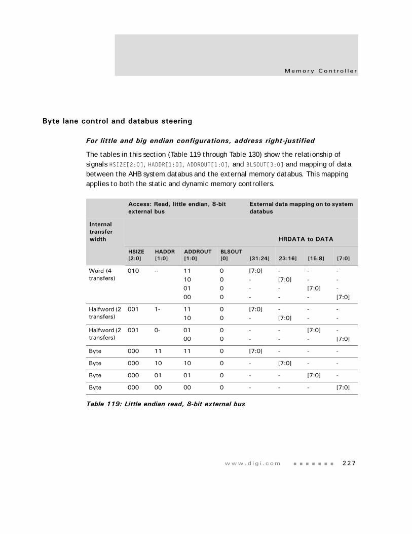
www.d i g i . com 227
Memo ry Con t r o l l e r
Byte lane control and databus steering
For little and big endian configurations, address right-justified
The tables in this section (Table 119 through Table 130) show the relationship of signals HSIZE[2:0], HADDR[1:0], ADDROUT[1:0], and BLSOUT[3:0] and mapping of data between the AHB system databus and the external memory databus. This mapping applies to both the static and dynamic memory controllers.
Access: Read, little endian, 8-bit external bus
External data mapping on to system databus
Internal transfer width HRDATA to DATA
HSIZE [2:0]
HADDR [1:0]
ADDROUT [1:0]
BLSOUT [0] [31:24] 23:16] [15:8] [7:0]
Word (4 transfers)
010 -- 11100100
0000
[7:0]---
-[7:0]--
--[7:0]-
---[7:0]
Halfword (2 transfers)
001 1- 1110
00
[7:0]-
-[7:0]
--
--
Halfword (2 transfers)
001 0- 0100
00
--
--
[7:0]-
-[7:0]
Byte 000 11 11 0 [7:0] - - -
Byte 000 10 10 0 - [7:0] - -
Byte 000 01 01 0 - - [7:0] -
Byte 000 00 00 0 - - - [7:0]
Table 119: Little endian read, 8-bit external bus
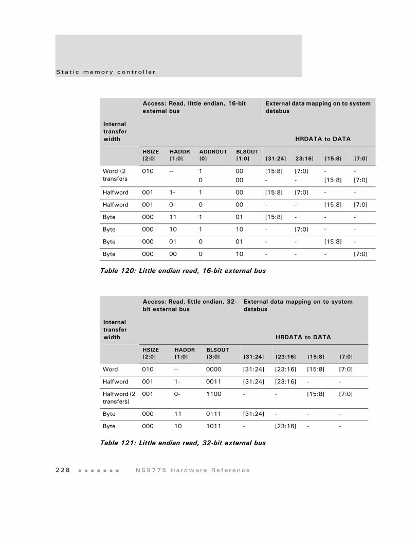
S t a t i c memo ry con t r o l l e r
2 2 8 NS9775 Ha r dwa r e Re f e r ence
Access: Read, little endian, 16-bit external bus
External data mapping on to system databus
Internal transfer width HRDATA to DATA
HSIZE [2:0]
HADDR [1:0]
ADDROUT [0]
BLSOUT [1:0] [31:24] 23:16] [15:8] [7:0]
Word (2 transfers
010 -- 10
0000
[15:8]-
[7:0]-
-[15:8]
-[7:0]
Halfword 001 1- 1 00 [15:8] [7:0] - -
Halfword 001 0- 0 00 - - [15:8] [7:0]
Byte 000 11 1 01 [15:8] - - -
Byte 000 10 1 10 - [7:0] - -
Byte 000 01 0 01 - - [15:8] -
Byte 000 00 0 10 - - - [7:0]
Table 120: Little endian read, 16-bit external bus
Access: Read, little endian, 32-bit external bus
External data mapping on to system databus
Internal transfer width HRDATA to DATA
HSIZE [2:0]
HADDR [1:0]
BLSOUT [3:0] [31:24] [23:16] [15:8] [7:0]
Word 010 -- 0000 [31:24] [23:16] [15:8] [7:0]
Halfword 001 1- 0011 [31:24] [23:16] - -
Halfword (2 transfers)
001 0- 1100 - - [15:8] [7:0]
Byte 000 11 0111 [31:24] - - -
Byte 000 10 1011 - [23:16] - -
Table 121: Little endian read, 32-bit external bus
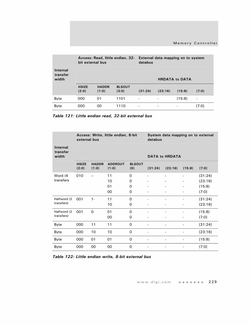
www.d i g i . com 229
Memo ry Con t r o l l e r
Byte 000 01 1101 - - [15:8] -
Byte 000 00 1110 - - - [7:0]
Access: Write, little endian, 8-bit external bus
System data mapping on to external databus
Internal transfer width DATA to HRDATA
HSIZE [2:0]
HADDR [1:0]
ADDROUT [1:0]
BLSOUT [0] [31:24] [23:16] [15:8] [7:0]
Word (4 transfers
010 -- 11100100
0000
----
----
----
[31:24][23:16][15:8][7:0]
Halfword (2 transfers)
001 1- 1110
00
--
--
--
[31:24][23:16]
Halfword (2 transfers)
001 0- 0100
00
--
--
--
[15:8][7:0]
Byte 000 11 11 0 - - - [31:24]
Byte 000 10 10 0 - - - [23:16]
Byte 000 01 01 0 - - - [15:8]
Byte 000 00 00 0 - - - [7:0]
Table 122: Little endian write, 8-bit external bus
Access: Read, little endian, 32-bit external bus
External data mapping on to system databus
Internal transfer width HRDATA to DATA
HSIZE [2:0]
HADDR [1:0]
BLSOUT [3:0] [31:24] [23:16] [15:8] [7:0]
Table 121: Little endian read, 32-bit external bus
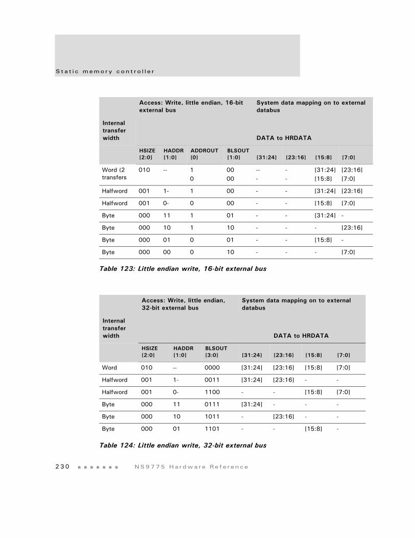
S t a t i c memo ry con t r o l l e r
2 3 0 NS9775 Ha r dwa r e Re f e r ence
Access: Write, little endian, 16-bit external bus
System data mapping on to external databus
Internal transfer width DATA to HRDATA
HSIZE [2:0]
HADDR [1:0]
ADDROUT [0]
BLSOUT [1:0] [31:24] [23:16] [15:8] [7:0]
Word (2 transfers
010 -- 10
0000
---
--
[31:24][15:8]
[23:16][7:0]
Halfword 001 1- 1 00 - - [31:24] [23:16]
Halfword 001 0- 0 00 - - [15:8] [7:0]
Byte 000 11 1 01 - - [31:24] -
Byte 000 10 1 10 - - - [23:16]
Byte 000 01 0 01 - - [15:8] -
Byte 000 00 0 10 - - - [7:0]
Table 123: Little endian write, 16-bit external bus
Access: Write, little endian, 32-bit external bus
System data mapping on to external databus
Internal transfer width DATA to HRDATA
HSIZE [2:0]
HADDR [1:0]
BLSOUT [3:0] [31:24] [23:16] [15:8] [7:0]
Word 010 -- 0000 [31:24] [23:16] [15:8] [7:0]
Halfword 001 1- 0011 [31:24] [23:16] - -
Halfword 001 0- 1100 - - [15:8] [7:0]
Byte 000 11 0111 [31:24] - - -
Byte 000 10 1011 - [23:16] - -
Byte 000 01 1101 - - [15:8] -
Table 124: Little endian write, 32-bit external bus
www.d i g i . com 231
Memo ry Con t r o l l e r
Byte 000 00 1110 - - - [7:0]
Access: Read, big endian, 8-bit external bus
External data mapping on to system databus
Internal transfer width HRDATA to DATA
HSIZE [2:0]
HADDR [1:0]
ADDROUT [1:0]
BLSOUT [0] [31:24] 23:16] [15:8] [7:0]
Word (4 transfers
010 -- 11100100
0000
---[7:0]
--[7:0]-
-[7:0]-
[7:0]---
Halfword (2 transfers)
001 1- 1110
00
--
--
-[7:0]
[7:0]-
Halfword (2 transfers)
001 0- 0100
00
-[7:0]
[7:0]-
--
--
Byte 000 11 11 0 - - - [7:0]
Byte 000 10 10 0 - - [7:0] -
Byte 000 01 01 0 - [7:0] - -
Byte 000 00 00 0 [7:0] - - -
Table 125: Big endian read, 8-bit external bus
Access: Write, little endian, 32-bit external bus
System data mapping on to external databus
Internal transfer width DATA to HRDATA
HSIZE [2:0]
HADDR [1:0]
BLSOUT [3:0] [31:24] [23:16] [15:8] [7:0]
Table 124: Little endian write, 32-bit external bus
S t a t i c memo ry con t r o l l e r
2 3 2 NS9775 Ha r dwa r e Re f e r ence
Access: Read, big endian, 16-bit external bus
External data mapping on to system databus
Internal transfer width HRDATA to DATA
HSIZE [2:0]
HADDR [1:0]
ADDROUT [0]
BLSOUT [1:0] [31:24] 23:16] [15:8] [7:0]
Word (2 transfers
010 -- 10
0000
-[15:8]
-[7:0]
[15:8]-
[7:0]-
Halfword 001 1- 1 00 - - [15:8] [7:0]
Halfword 001 0- 0 00 [15:8] [7:0] - -
Byte 000 11 1 10 - - - [7:0]
Byte 000 10 1 01 - - [15:8] -
Byte 000 01 0 10 - [7:0] - -
Byte 000 00 0 01 [15:8] - - -
Table 126: Big endian read, 16-bit external bus
Access: Read, big endian, 32-bit external bus
External data mapping on to system databus
Internal transfer width HRDATA to DATA
HSIZE [2:0]
HADDR [1:0]
BLSOUT [3:0] [31:24] [23:16] [15:8] [7:0]
Word 010 -- 0000 [31:24] [23:16] [15:8] [7:0]
Halfword 001 1- 1100 - - [15:8] [7:0]
Halfword (2 transfers)
001 0- 0011 [31:24] [23:16] - -
Byte 000 11 1110 - - - [7:0]
Table 127: Big endian read, 32-bit external bus
www.d i g i . com 233
Memo ry Con t r o l l e r
Byte 000 10 1101 - - [15:8] -
Byte 000 01 1011 - [23:16] - -
Byte 000 00 0111 [31:24] - - -
Access: Write, big endian, 8-bit external bus
System data mapping on to external databus
Internal transfer width DATA to HRDATA
HSIZE [2:0]
HADDR [1:0]
ADDROUT [1:0]
BLSOUT [0] [31:24] [23:16] [15:8] [7:0]
Word (4 transfers
010 -- 11100100
0000
----
----
----
[7:0][15:8][23:16][31:24]
Halfword (2 transfers)
001 1- 1110
00
--
--
--
[7:0][15:8]
Halfword (2 transfers)
001 0- 0100
00
--
--
--
[23:16][31:24]
Byte 000 11 11 0 - - - [7:0]
Byte 000 10 10 0 - - - [15:8]
Byte 000 01 01 0 - - - [23:16]
Byte 000 00 00 0 - - - [31:24]
Table 128: Big endian write, 8-bit external bus
Access: Read, big endian, 32-bit external bus
External data mapping on to system databus
Internal transfer width HRDATA to DATA
HSIZE [2:0]
HADDR [1:0]
BLSOUT [3:0] [31:24] [23:16] [15:8] [7:0]
Table 127: Big endian read, 32-bit external bus
S t a t i c memo ry con t r o l l e r
2 3 4 NS9775 Ha r dwa r e Re f e r ence
Access: Write, big endian, 16-bit external bus
System data mapping on to external databus
Internal transfer width DATA to HRDATA
HSIZE [2:0]
HADDR [1:0]
ADDROUT [0]
BLSOUT [1:0] [31:24] [23:16] [15:8] [7:0]
Word (2 transfers
010 -- 10
0000
---
--
[15:8][31:24]
[7:0][23:16]
Halfword 001 1- 1 00 - - [15:8] [7:0]
Halfword 001 0- 0 00 - - [31:24] [23:16]
Byte 000 11 1 10 - - - [7:0]
Byte 000 10 1 01 - - [15:8] -
Byte 000 01 0 10 - - - [23:16]
Byte 000 00 0 01 - - [31:24] -
Table 129: Big endian write, 16-bit external bus
Access: Write, big endian, 32-bit external bus
System data mapping on to external databus
Internal transfer width DATA
HSIZE [2:0]
HADDR [1:0]
BLSOUT [3:0] [31:24] [23:16] [15:8] [7:0]
Word 010 -- 0000 [31:24] [23:16] [15:8] [7:0]
Halfword 001 1- 1100 - - [15:8] [7:0]
Halfword 001 0- 0011 [31:24] [23:16] - -
Byte 000 11 1110 - - - [7:0]
Byte 000 10 1101 - - [15:8] -
Byte 000 01 1011 - [23:16] - -
Table 130: Big endian write, 32-bit external bus
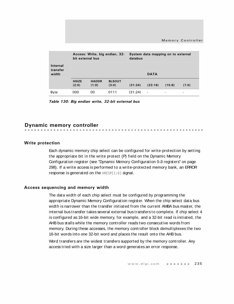
www.d i g i . com 235
Memo ry Con t r o l l e r
Dynamic memory controller
Write protection
Each dynamic memory chip select can be configured for write-protection by setting the appropriate bit in the write protect (P) field on the Dynamic Memory Configuration register (see "Dynamic Memory Configuration 0–3 registers" on page 298). If a write access is performed to a write-protected memory bank, an ERROR response is generated on the HRESP[1:0] signal.
Access sequencing and memory width
The data width of each chip select must be configured by programming the appropriate Dynamic Memory Configuration register. When the chip select data bus width is narrower than the transfer initiated from the current AMBA bus master, the internal bus transfer takes several external bus transfers to complete. If chip select 4 is configured as 16-bit wide memory, for example, and a 32-bit read is initiated, the AHB bus stalls while the memory controller reads two consecutive words from memory. During these accesses, the memory controller block demultiplexes the two 16-bit words into one 32-bit word and places the result onto the AHB bus.
Word transfers are the widest transfers supported by the memory controller. Any access tried with a size larger than a word generates an error response.
Byte 000 00 0111 [31:24] - - -
Access: Write, big endian, 32-bit external bus
System data mapping on to external databus
Internal transfer width DATA
HSIZE [2:0]
HADDR [1:0]
BLSOUT [3:0] [31:24] [23:16] [15:8] [7:0]
Table 130: Big endian write, 32-bit external bus
Dynam i c memo ry con t r o l l e r
2 3 6 NS9775 Ha r dwa r e Re f e r ence
Address mapping
This section provides tables that show how AHB address bus addresses map to the external dynamic memory address ADDROUT[14:0] for different memory configurations and bus widths. The address mapping is selected by programming the address mapping bits in the Dynamic Memory Configuration registers (see "Dynamic Memory Configuration 0–3 registers" on page 298).
The information provided includes:
Memory controller output address (ADDROUT). Indicates the address lines output from the memory controller.
Memory device connections. Indicate the device signals that must be connected to the memory controller AddrOut lines.
AHB addresses to row address. Indicates the input HADDR address bits used from the AHB transfer for the row access.
AHB address to column address. Indicates the input HADDR address bits used from the AHB transfer for the column access.
Notes:For all tables in this section:
– ** indicates that the bit is controlled by the SDRAM controller. The SDRAM controller always transfers 32-bits of data at a time. For chip selects with a 16-bit wide databus, the SDRAM controller performs two transfers: a column transfer with the lowest bit set to 0 and a column transfer with the lowest bit set to 1.
– BA, BA0, and BA1 indicate the bank address signals. AP indicates the auto precharge signal (usually, address bit 10).
Separate tables are provided for two different address mapping schemes: row, bank, column (RBC) or bank, row, column (BRC), and for 32-bit and 16-bit wide buses:
– 32-bit wide databus address mappings, SDRAM (RBC) (see "32-bit wide databus address mappings, SDRAM (RBC)" on page 237). These address mappings are used for 32-bit data bus chip select with SDR-SDRAM memory devices. The row-bank-column address mapping scheme allows memory accesses to be performed efficiently to nearby memory regions.
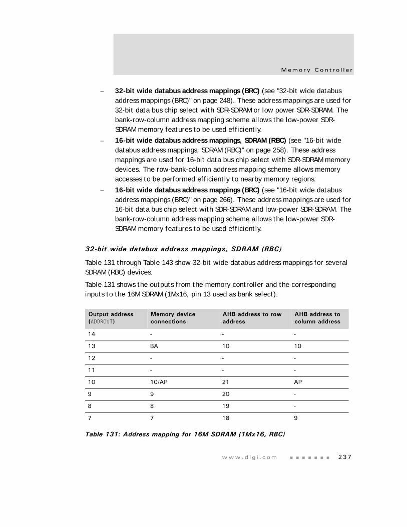
www.d i g i . com 237
Memo ry Con t r o l l e r
– 32-bit wide databus address mappings (BRC) (see "32-bit wide databus address mappings (BRC)" on page 248). These address mappings are used for 32-bit data bus chip select with SDR-SDRAM or low power SDR-SDRAM. The bank-row-column address mapping scheme allows the low-power SDR-SDRAM memory features to be used efficiently.
– 16-bit wide databus address mappings, SDRAM (RBC) (see "16-bit wide databus address mappings, SDRAM (RBC)" on page 258). These address mappings are used for 16-bit data bus chip select with SDR-SDRAM memory devices. The row-bank-column address mapping scheme allows memory accesses to be performed efficiently to nearby memory regions.
– 16-bit wide databus address mappings (BRC) (see "16-bit wide databus address mappings (BRC)" on page 266). These address mappings are used for 16-bit data bus chip select with SDR-SDRAM and low-power SDR-SDRAM. The bank-row-column address mapping scheme allows the low-power SDR-SDRAM memory features to be used efficiently.
32-bit wide databus address mappings, SDRAM (RBC)
Table 131 through Table 143 show 32-bit wide databus address mappings for several SDRAM (RBC) devices.
Table 131 shows the outputs from the memory controller and the corresponding inputs to the 16M SDRAM (1Mx16, pin 13 used as bank select).
Output address (ADDROUT)
Memory device connections
AHB address to row address
AHB address to column address
14 - - -
13 BA 10 10
12 - - -
11 - - -
10 10/AP 21 AP
9 9 20 -
8 8 19 -
7 7 18 9
Table 131: Address mapping for 16M SDRAM (1Mx16, RBC)
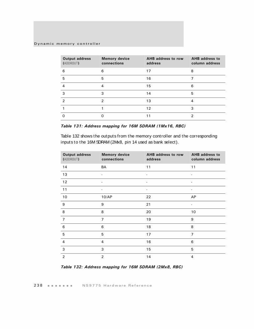
Dynam i c memo ry con t r o l l e r
2 3 8 NS9775 Ha r dwa r e Re f e r ence
Table 132 shows the outputs from the memory controller and the corresponding inputs to the 16M SDRAM (2Mx8, pin 14 used as bank select).
6 6 17 8
5 5 16 7
4 4 15 6
3 3 14 5
2 2 13 4
1 1 12 3
0 0 11 2
Output address (ADDROUT)
Memory device connections
AHB address to row address
AHB address to column address
14 BA 11 11
13 - - -
12 - - -
11 - - -
10 10/AP 22 AP
9 9 21 -
8 8 20 10
7 7 19 9
6 6 18 8
5 5 17 7
4 4 16 6
3 3 15 5
2 2 14 4
Table 132: Address mapping for 16M SDRAM (2Mx8, RBC)
Output address (ADDROUT)
Memory device connections
AHB address to row address
AHB address to column address
Table 131: Address mapping for 16M SDRAM (1Mx16, RBC)
www.d i g i . com 239
Memo ry Con t r o l l e r
Table 133 shows the outputs from the memory controller and the corresponding inputs to the 64M SDRAM (2Mx32, pins 13 and 14 used as bank selects).
Table 134 shows the outputs from the memory controller and the corresponding inputs to the 64M SDRAM (4Mx16, pins 13 and 14 used as bank selects).
1 1 13 3
0 0 12 2
Output address (ADDROUT)
Memory device connections
AHB address to row address
AHB address to column address
14 BA1 11 11
13 BA0 10 10
12 - - -
11 - - -
10 10/AP 22 AP
9 9 21 -
8 8 20 -
7 7 19 9
6 6 18 8
5 5 17 7
4 4 16 6
3 3 15 5
2 2 14 4
1 1 13 3
0 0 12 2
Table 133: Address mapping for 64M SDRAM (2Mx32, RBC)
Output address (ADDROUT)
Memory device connections
AHB address to row address
AHB address to column address
Table 132: Address mapping for 16M SDRAM (2Mx8, RBC)
Dynam i c memo ry con t r o l l e r
2 4 0 NS9775 Ha r dwa r e Re f e r ence
Output address (ADDROUT)
Memory device connections
AHB address to row address
AHB address to column address
14 BA1 11 11
13 BA0 10 10
12 - - -
11 11 23 -
10 10/AP 22 AP
9 9 21 -
8 8 20 -
7 7 199 9
6 6 18 8
5 5 17 7
4 4 16 6
3 3 15 5
2 2 14 4
1 1 13 3
0 0 12 2
Table 134: Address mapping for 64M SDRAM (4Mx16, RBC)

www.d i g i . com 241
Memo ry Con t r o l l e r
Table 135 shows the outputs from the memory controller and the corresponding inputs to the 64 M SDRAM (8Mx8, pins 13 and 14 used as bank selects).
Table 136 shows the outputs from the memory controller and the corresponding inputs to the 128M SDRAM (4Mx32, pins 13 and 14 used as bank selects).
Output address (ADDROUT)
Memory device connections
AHB address to row address
AHB address to column address
14 BA1 11 11
13 BA0 12 12
12 - - -
11 11 24 -
10 10/AP 23 AP
9 9 22 -
8 8 21 10
7 7 20 9
6 6 19 8
5 5 18 7
4 4 17 6
3 3 16 5
2 2 15 4
1 1 14 3
0 0 13 2
Table 135: Address mapping for 64M SDRAM (8Mx8, RBC)
Output address (ADDROUT)
Memory device connections
AHB address to row address
AHB address to column address
14 BA1 11 11
13 BA0 10 10
12 - - -
Table 136: Address mapping for 128M SDRAM (4Mx32, RBC)

Dynam i c memo ry con t r o l l e r
2 4 2 NS9775 Ha r dwa r e Re f e r ence
Table 137 shows the outputs from the memory controller and the corresponding inputs to the 64M SDRAM (8Mx16, pins 13 and 14 used as bank selects).
11 11 23 -
10 10/AP 22 AP
9 9 21 -
8 8 20 -
7 7 19 9
6 6 18 8
5 5 17 7
4 4 16 6
3 3 15 5
2 2 14 4
1 1 13 3
0 0 12 2
Output address (ADDROUT)
Memory device connections
AHB address to row address
AHB address to column address
14 BA1 11 11
13 BA0 12 12
12 - - -
11 11 24 -
10 10/AP 23 AP
9 9 22 -
8 8 21 10
7 7 20 9
Table 137: Address mapping for 128 SDRAM (8Mx16, RBC)
Output address (ADDROUT)
Memory device connections
AHB address to row address
AHB address to column address
Table 136: Address mapping for 128M SDRAM (4Mx32, RBC)
www.d i g i . com 243
Memo ry Con t r o l l e r
Table 138 shows the outputs from the memory controller and the corresponding inputs to the 128M SDRAM (16Mx8, pins 13 and 14 used as bank selects).
6 6 19 8
5 5 18 7
4 4 17 6
3 3 16 5
2 2 15 4
1 1 14 3
0 0 13 2
Output address (ADDROUT)
Memory device connections
AHB address to row address
AHB address to column address
14 BA1 13 13
13 BA0 12 12
12 12 - -
11 11 25 -
10 10/AP 24 AP
9 9 23 11
8 8 22 10
7 7 21 9
6 6 20 8
5 5 19 7
4 4 18 6
3 3 17 5
2 2 16 4
Table 138: Address mapping for 128 SDRAM (16Mx8, RBC)
Output address (ADDROUT)
Memory device connections
AHB address to row address
AHB address to column address
Table 137: Address mapping for 128 SDRAM (8Mx16, RBC)
Dynam i c memo ry con t r o l l e r
2 4 4 NS9775 Ha r dwa r e Re f e r ence
Table 139 shows the outputs from the memory controller and the corresponding inputs to the 256M SDRAM (8Mx32, pins 13 and 14 used as bank selects).
1 1 15 3
0 0 14 2
Output address (ADDROUT)
Memory device connections
AHB address to row address
AHB address to column address
14 BA1 11 11
13 BA0 10 10
12 12 24 -
11 11 23 -
10 10/AP 22 AP
9 9 21 -
8 8 20 -
7 7 19 9
6 6 18 8
5 5 17 7
4 4 16 6
3 3 15 5
2 2 14 4
1 1 13 3
0 0 12 2
Table 139: Address mapping for 256 SDRAM (8Mx32, RBC)
Output address (ADDROUT)
Memory device connections
AHB address to row address
AHB address to column address
Table 138: Address mapping for 128 SDRAM (16Mx8, RBC)
www.d i g i . com 245
Memo ry Con t r o l l e r
Table 140 shows the outputs from the memory controller and the corresponding inputs to the 256M SDRAM (16Mx16, pins 13 and 14 used as bank selects).
Table 141 shows the outputs from the memory controller and the corresponding inputs to the 256M SDRAM (32Mx8, pins 13 and 14 used as bank selects).
Output address (ADDROUT)
Memory device connections
AHB address to row address
AHB address to column address
14 BA1 11 11
13 BA0 12 12
12 12 25 -
11 11 24 -
10 10/AP 23 AP
9 9 22 -
8 8 21 10
7 7 20 9
6 6 19 8
5 5 18 7
4 4 17 6
3 3 16 5
2 2 15 4
1 1 14 3
0 0 13 2
Table 140: Address mapping for 256M SDRAM (16Mx16, RBC)
Output address (ADDROUT)
Memory device connections
AHB address to row address
AHB address to column address
14 BA1 13 13
13 BA0 12 12
12 12 26 -
Table 141: Address mapping for 256M SDRAM (32Mx8, RBC)
Dynam i c memo ry con t r o l l e r
2 4 6 NS9775 Ha r dwa r e Re f e r ence
Table 142 shows the outputs from the memory controller and the corresponding inputs to the 512M SDRAM (32Mx16, pins 13 and 14 used as bank selects).
11 11 25 -
10 10/AP 24 AP
9 9 23 11
8 8 22 10
7 7 21 9
6 6 20 8
5 5 19 7
4 4 18 6
3 3 17 5
2 2 16 4
1 1 15 3
0 0 14 2
Output address (ADDROUT)
Memory device connections
AHB address to row address
AHB address to column address
14 BA1 13 13
13 BA0 12 12
12 12 26 -
11 11 25 -
10 10/AP 24 AP
9 9 23 11
8 8 22 10
7 7 21 9
Table 142: Address mapping for 512M SDRAM (32Mx16, RBC)
Output address (ADDROUT)
Memory device connections
AHB address to row address
AHB address to column address
Table 141: Address mapping for 256M SDRAM (32Mx8, RBC)
www.d i g i . com 247
Memo ry Con t r o l l e r
Table 143 shows the outputs from the memory controller and the corresponding inputs to the 512M SDRAM (64Mx8, pins 13 and 14 used as bank selects).
6 6 20 8
5 5 19 7
4 4 18 6
3 3 17 5
2 2 16 4
1 1 15 3
0 0 14 2
Output address (ADDROUT)
Memory device connections
AHB address to row address
AHB address to column address
14 BA1 13 13
13 BA0 14 14
12 12 27 -
11 11 26 12
10 10/AP 25 AP
9 9 24 11
8 8 23 10
7 7 22 9
6 6 21 8
5 5 20 7
4 4 19 6
3 3 18 5
2 2 17 4
Table 143: Address mapping for 512M SDRAM (64Mx8, RBC)
Output address (ADDROUT)
Memory device connections
AHB address to row address
AHB address to column address
Table 142: Address mapping for 512M SDRAM (32Mx16, RBC)
Dynam i c memo ry con t r o l l e r
2 4 8 NS9775 Ha r dwa r e Re f e r ence
32-bit wide databus address mappings (BRC)
Table 144 through Table 156 show 32-bit wide databus address mappings for several SDRAM (BRC) devices.
Table 144 shows the outputs from the memory controller and the corresponding inputs to the 16M SDRAM (1x16, pin 14 used as bank select).
1 1 16 3
0 0 15 2
Output address (ADDROUT)
Memory device connections
AHB address to row address
AHB address to column address
14 BA 21 21
13 - - -
12 - - -
11 - - -
10 10/AP 20 AP
9 9 19 -
8 8 18 -
7 7 17 9
6 6 16 8
5 5 15 7
4 4 14 6
3 3 13 5
2 2 12 4
1 1 11 3
0 0 10 2
Table 144: Address mapping for 16M SDRAM (1Mx16, BRC)
Output address (ADDROUT)
Memory device connections
AHB address to row address
AHB address to column address
Table 143: Address mapping for 512M SDRAM (64Mx8, RBC)

www.d i g i . com 249
Memo ry Con t r o l l e r
Table 145 shows the outputs from the memory controller and the corresponding inputs to the 16M SDRAM (2Mx8, pin 13 used as bank select).
Table 146 shows the outputs from the memory controller and the corresponding inputs to the 64M SDRAM (2Mx32, pins 13 and 14 used as bank selects).
Output address (ADDROUT)
Memory device connections
AHB address to row address
AHB address to column address
14 - - -
13 BA 22 22
12 - - -
11 - - -
10 10/AP 21 AP
9 9 20 -
8 8 19 10
7 7 18 9
6 6 17 8
5 5 16 7
4 4 15 6
3 3 14 5
2 2 13 4
1 1 12 3
0 0 11 2
Table 145: Address mapping for 16M SDRAM (2Mx8, BRC)
Output address (ADDROUT)
Memory device connections
AHB address to row address
AHB address to column address
14 BA1 21 21
13 BA0 22 22
12 - - -
Table 146: Address mapping for 64M SDRAM (2Mx32, BRC)

Dynam i c memo ry con t r o l l e r
2 5 0 NS9775 Ha r dwa r e Re f e r ence
Table 147 shows the outputs from the memory controller and the corresponding inputs to the 64M SDRAM (4Mx16, pins 13 and 14 used as bank selects).
11 - - -
10 10/AP 20 AP
9 9 19 -
8 8 18 -
7 7 17 9
6 6 16 8
5 5 15 7
4 4 14 6
3 3 13 5
2 2 12 4
1 1 11 3
0 0 10 2
Output address (ADDROUT)
Memory device connections
AHB address to row address
AHB address to column address
14 BA1 23 23
13 BA0 22 22
12 - - -
11 11 21 -
10 10/AP 20 AP
9 9 19 -
8 8 18 -
7 7 17 9
Table 147: Address mapping for 64M SDRAM (4Mx16, BRC)
Output address (ADDROUT)
Memory device connections
AHB address to row address
AHB address to column address
Table 146: Address mapping for 64M SDRAM (2Mx32, BRC)

www.d i g i . com 251
Memo ry Con t r o l l e r
Table 148 shows the outputs from the memory controller and the corresponding inputs to the 64M SDRAM (8Mx8, pins 13 and 14 used as bank selects).
6 6 16 8
5 5 15 7
4 4 14 6
3 3 13 5
2 2 12 4
1 1 11 3
0 0 10 2
Output address (ADDROUT)
Memory device connections
AHB address to row address
AHB address to column address
14 BA1 23 23
13 BA0 24 24
12 - - -
11 11 22 -
10 10/AP 21 AP
9 9 20 -
8 8 19 10
7 7 18 9
6 6 17 8
5 5 16 7
4 4 15 6
3 3 14 5
2 2 13 4
Table 148: Address mapping for 64M SDRAM (8Mx8, BRC)
Output address (ADDROUT)
Memory device connections
AHB address to row address
AHB address to column address
Table 147: Address mapping for 64M SDRAM (4Mx16, BRC)

Dynam i c memo ry con t r o l l e r
2 5 2 NS9775 Ha r dwa r e Re f e r ence
Table 149 shows the outputs from the memory controller and the corresponding inputs to the 128M SDSRAM (4Mx32, pins 13 and 14 used as bank selects).
1 1 12 3
0 0 11 2
Output address (ADDROUT)
Memory device connections
AHB address to row address
AHB address to column address
14 BA1 23 23
13 BA0 22 22
12 - - -
11 11 21 -
10 10/AP 20 AP
9 9 19 -
8 8 18 -
7 7 17 9
6 6 16 8
5 5 15 7
4 4 14 6
3 3 13 5
2 2 12 4
1 1 11 3
0 0 10 2
Table 149: Address mapping for 128M SDRAM (4Mx32, BRC)
Output address (ADDROUT)
Memory device connections
AHB address to row address
AHB address to column address
Table 148: Address mapping for 64M SDRAM (8Mx8, BRC)
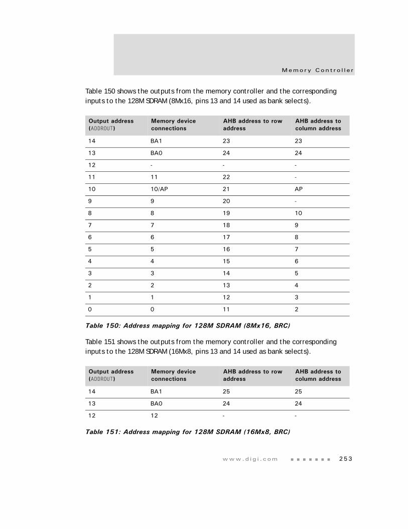
www.d i g i . com 253
Memo ry Con t r o l l e r
Table 150 shows the outputs from the memory controller and the corresponding inputs to the 128M SDRAM (8Mx16, pins 13 and 14 used as bank selects).
Table 151 shows the outputs from the memory controller and the corresponding inputs to the 128M SDRAM (16Mx8, pins 13 and 14 used as bank selects).
Output address (ADDROUT)
Memory device connections
AHB address to row address
AHB address to column address
14 BA1 23 23
13 BA0 24 24
12 - - -
11 11 22 -
10 10/AP 21 AP
9 9 20 -
8 8 19 10
7 7 18 9
6 6 17 8
5 5 16 7
4 4 15 6
3 3 14 5
2 2 13 4
1 1 12 3
0 0 11 2
Table 150: Address mapping for 128M SDRAM (8Mx16, BRC)
Output address (ADDROUT)
Memory device connections
AHB address to row address
AHB address to column address
14 BA1 25 25
13 BA0 24 24
12 12 - -
Table 151: Address mapping for 128M SDRAM (16Mx8, BRC)
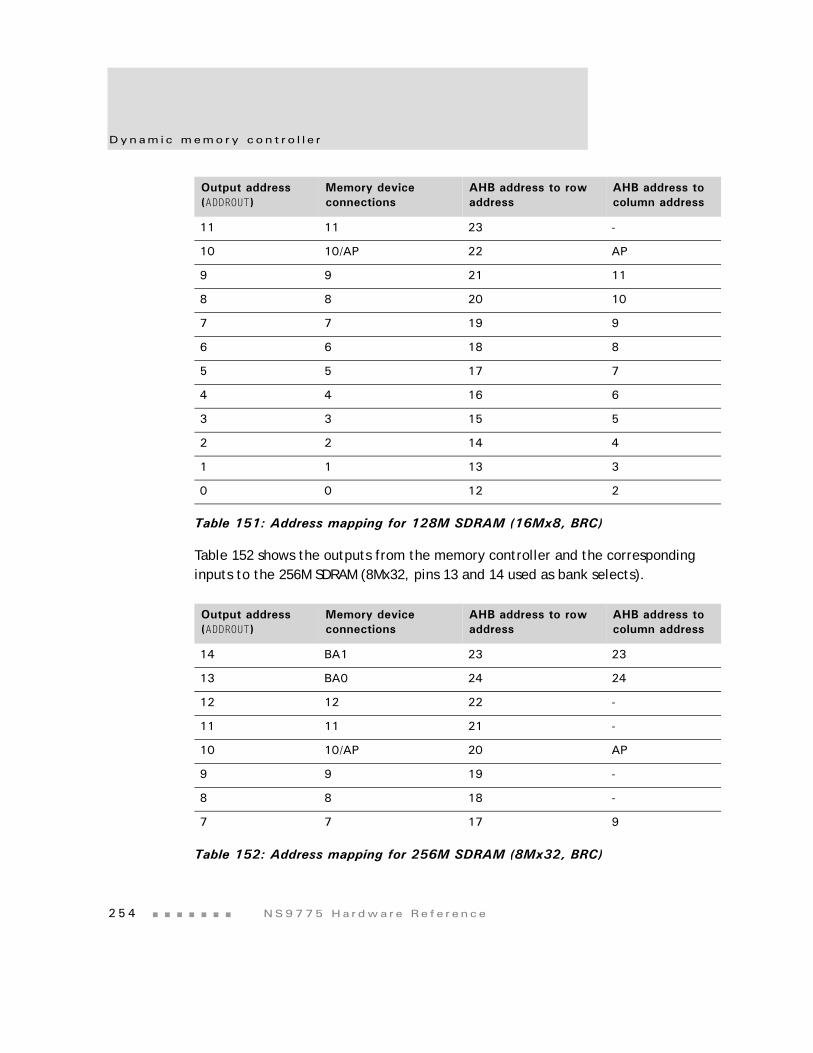
Dynam i c memo ry con t r o l l e r
2 5 4 NS9775 Ha r dwa r e Re f e r ence
Table 152 shows the outputs from the memory controller and the corresponding inputs to the 256M SDRAM (8Mx32, pins 13 and 14 used as bank selects).
11 11 23 -
10 10/AP 22 AP
9 9 21 11
8 8 20 10
7 7 19 9
6 6 18 8
5 5 17 7
4 4 16 6
3 3 15 5
2 2 14 4
1 1 13 3
0 0 12 2
Output address (ADDROUT)
Memory device connections
AHB address to row address
AHB address to column address
14 BA1 23 23
13 BA0 24 24
12 12 22 -
11 11 21 -
10 10/AP 20 AP
9 9 19 -
8 8 18 -
7 7 17 9
Table 152: Address mapping for 256M SDRAM (8Mx32, BRC)
Output address (ADDROUT)
Memory device connections
AHB address to row address
AHB address to column address
Table 151: Address mapping for 128M SDRAM (16Mx8, BRC)
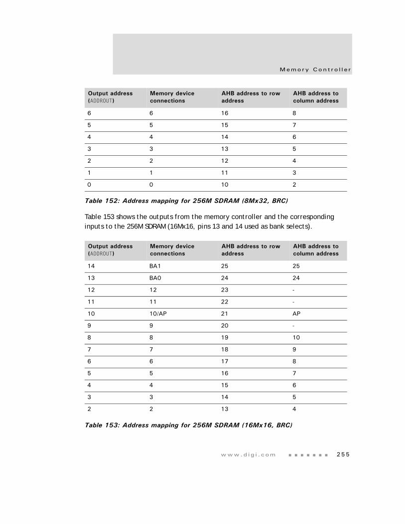
www.d i g i . com 255
Memo ry Con t r o l l e r
Table 153 shows the outputs from the memory controller and the corresponding inputs to the 256M SDRAM (16Mx16, pins 13 and 14 used as bank selects).
6 6 16 8
5 5 15 7
4 4 14 6
3 3 13 5
2 2 12 4
1 1 11 3
0 0 10 2
Output address (ADDROUT)
Memory device connections
AHB address to row address
AHB address to column address
14 BA1 25 25
13 BA0 24 24
12 12 23 -
11 11 22 -
10 10/AP 21 AP
9 9 20 -
8 8 19 10
7 7 18 9
6 6 17 8
5 5 16 7
4 4 15 6
3 3 14 5
2 2 13 4
Table 153: Address mapping for 256M SDRAM (16Mx16, BRC)
Output address (ADDROUT)
Memory device connections
AHB address to row address
AHB address to column address
Table 152: Address mapping for 256M SDRAM (8Mx32, BRC)
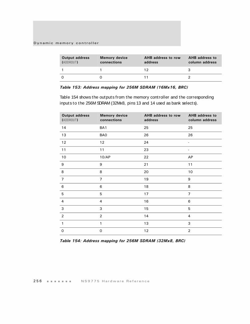
Dynam i c memo ry con t r o l l e r
2 5 6 NS9775 Ha r dwa r e Re f e r ence
Table 154 shows the outputs from the memory controller and the corresponding inputs to the 256M SDRAM (32Mx8, pins 13 and 14 used as bank selects).
1 1 12 3
0 0 11 2
Output address (ADDROUT)
Memory device connections
AHB address to row address
AHB address to column address
14 BA1 25 25
13 BA0 26 26
12 12 24 -
11 11 23 -
10 10/AP 22 AP
9 9 21 11
8 8 20 10
7 7 19 9
6 6 18 8
5 5 17 7
4 4 16 6
3 3 15 5
2 2 14 4
1 1 13 3
0 0 12 2
Table 154: Address mapping for 256M SDRAM (32Mx8, BRC)
Output address (ADDROUT)
Memory device connections
AHB address to row address
AHB address to column address
Table 153: Address mapping for 256M SDRAM (16Mx16, BRC)
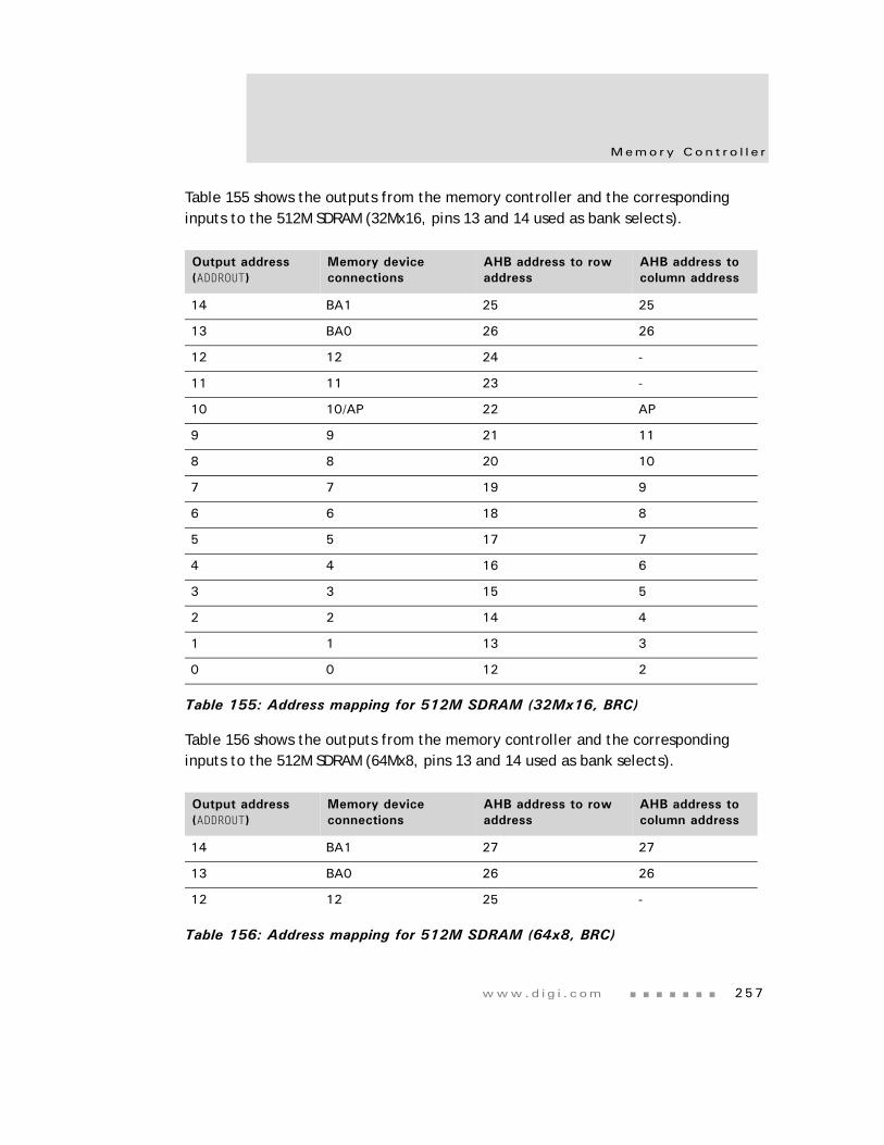
www.d i g i . com 257
Memo ry Con t r o l l e r
Table 155 shows the outputs from the memory controller and the corresponding inputs to the 512M SDRAM (32Mx16, pins 13 and 14 used as bank selects).
Table 156 shows the outputs from the memory controller and the corresponding inputs to the 512M SDRAM (64Mx8, pins 13 and 14 used as bank selects).
Output address (ADDROUT)
Memory device connections
AHB address to row address
AHB address to column address
14 BA1 25 25
13 BA0 26 26
12 12 24 -
11 11 23 -
10 10/AP 22 AP
9 9 21 11
8 8 20 10
7 7 19 9
6 6 18 8
5 5 17 7
4 4 16 6
3 3 15 5
2 2 14 4
1 1 13 3
0 0 12 2
Table 155: Address mapping for 512M SDRAM (32Mx16, BRC)
Output address (ADDROUT)
Memory device connections
AHB address to row address
AHB address to column address
14 BA1 27 27
13 BA0 26 26
12 12 25 -
Table 156: Address mapping for 512M SDRAM (64x8, BRC)
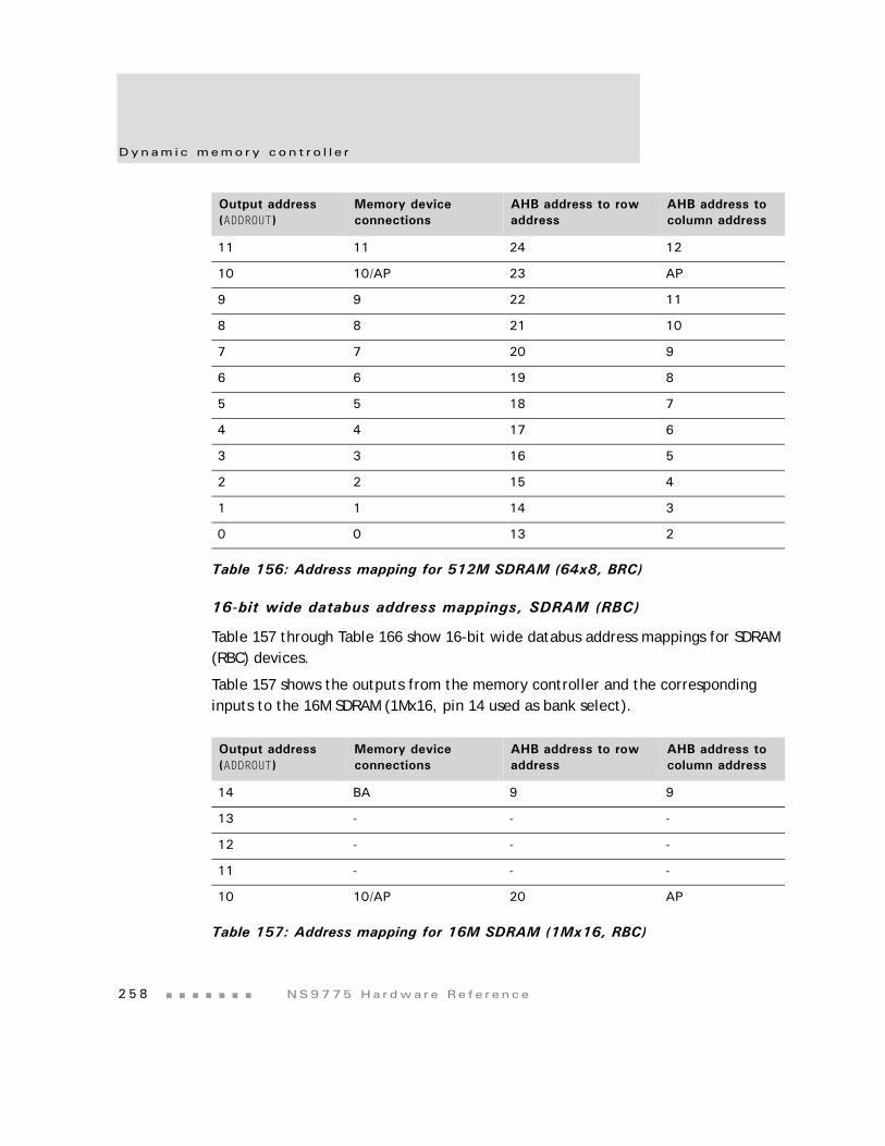
Dynam i c memo ry con t r o l l e r
2 5 8 NS9775 Ha r dwa r e Re f e r ence
16-bit wide databus address mappings, SDRAM (RBC)
Table 157 through Table 166 show 16-bit wide databus address mappings for SDRAM (RBC) devices.
Table 157 shows the outputs from the memory controller and the corresponding inputs to the 16M SDRAM (1Mx16, pin 14 used as bank select).
11 11 24 12
10 10/AP 23 AP
9 9 22 11
8 8 21 10
7 7 20 9
6 6 19 8
5 5 18 7
4 4 17 6
3 3 16 5
2 2 15 4
1 1 14 3
0 0 13 2
Output address (ADDROUT)
Memory device connections
AHB address to row address
AHB address to column address
14 BA 9 9
13 - - -
12 - - -
11 - - -
10 10/AP 20 AP
Table 157: Address mapping for 16M SDRAM (1Mx16, RBC)
Output address (ADDROUT)
Memory device connections
AHB address to row address
AHB address to column address
Table 156: Address mapping for 512M SDRAM (64x8, BRC)
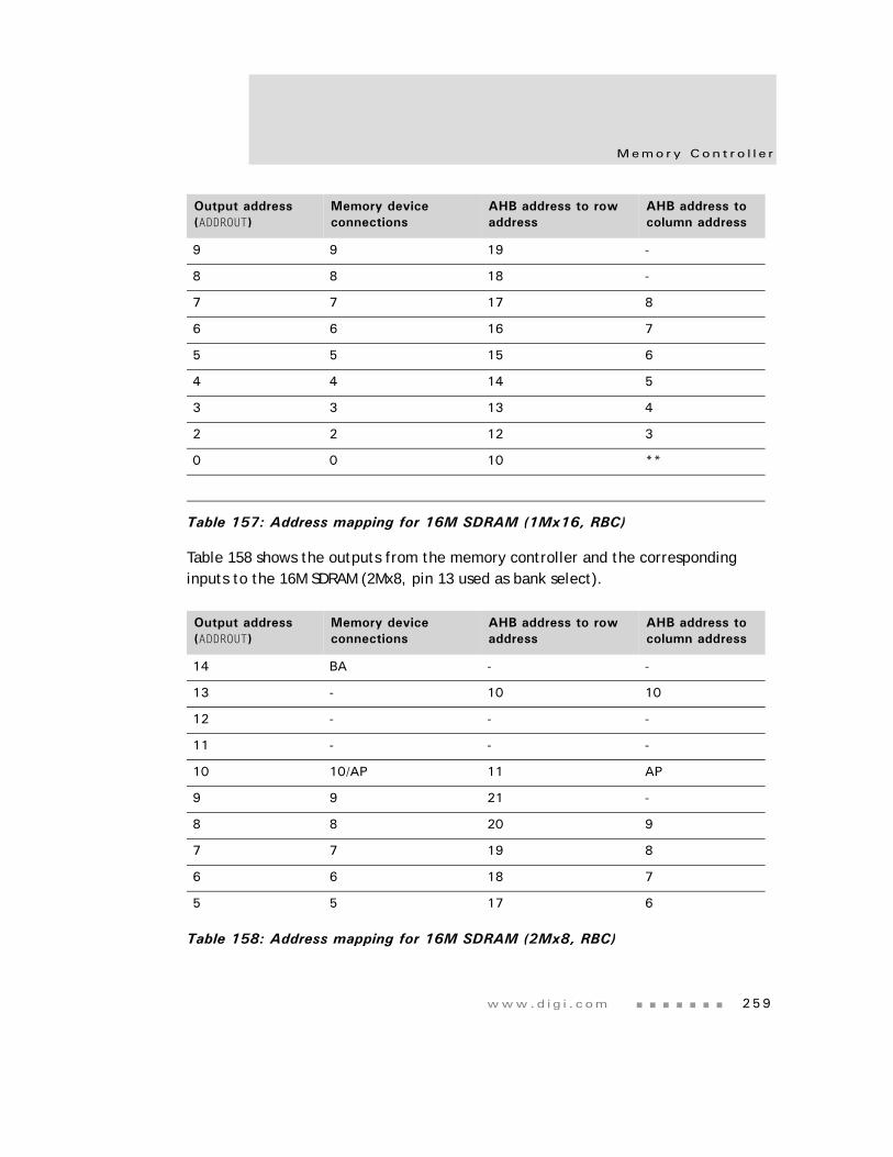
www.d i g i . com 259
Memo ry Con t r o l l e r
Table 158 shows the outputs from the memory controller and the corresponding inputs to the 16M SDRAM (2Mx8, pin 13 used as bank select).
9 9 19 -
8 8 18 -
7 7 17 8
6 6 16 7
5 5 15 6
4 4 14 5
3 3 13 4
2 2 12 3
0 0 10 **
Output address (ADDROUT)
Memory device connections
AHB address to row address
AHB address to column address
14 BA - -
13 - 10 10
12 - - -
11 - - -
10 10/AP 11 AP
9 9 21 -
8 8 20 9
7 7 19 8
6 6 18 7
5 5 17 6
Table 158: Address mapping for 16M SDRAM (2Mx8, RBC)
Output address (ADDROUT)
Memory device connections
AHB address to row address
AHB address to column address
Table 157: Address mapping for 16M SDRAM (1Mx16, RBC)
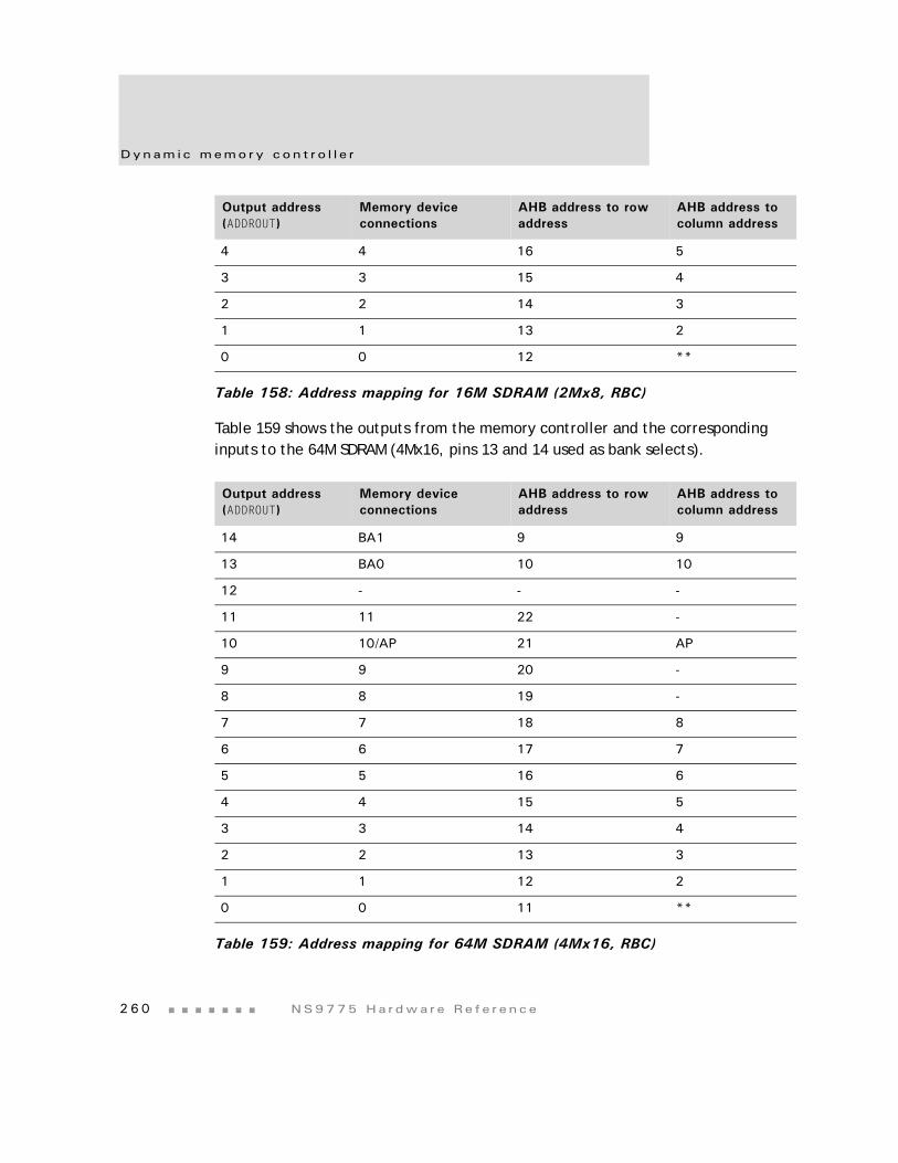
Dynam i c memo ry con t r o l l e r
2 6 0 NS9775 Ha r dwa r e Re f e r ence
Table 159 shows the outputs from the memory controller and the corresponding inputs to the 64M SDRAM (4Mx16, pins 13 and 14 used as bank selects).
4 4 16 5
3 3 15 4
2 2 14 3
1 1 13 2
0 0 12 **
Output address (ADDROUT)
Memory device connections
AHB address to row address
AHB address to column address
14 BA1 9 9
13 BA0 10 10
12 - - -
11 11 22 -
10 10/AP 21 AP
9 9 20 -
8 8 19 -
7 7 18 8
6 6 17 7
5 5 16 6
4 4 15 5
3 3 14 4
2 2 13 3
1 1 12 2
0 0 11 **
Table 159: Address mapping for 64M SDRAM (4Mx16, RBC)
Output address (ADDROUT)
Memory device connections
AHB address to row address
AHB address to column address
Table 158: Address mapping for 16M SDRAM (2Mx8, RBC)
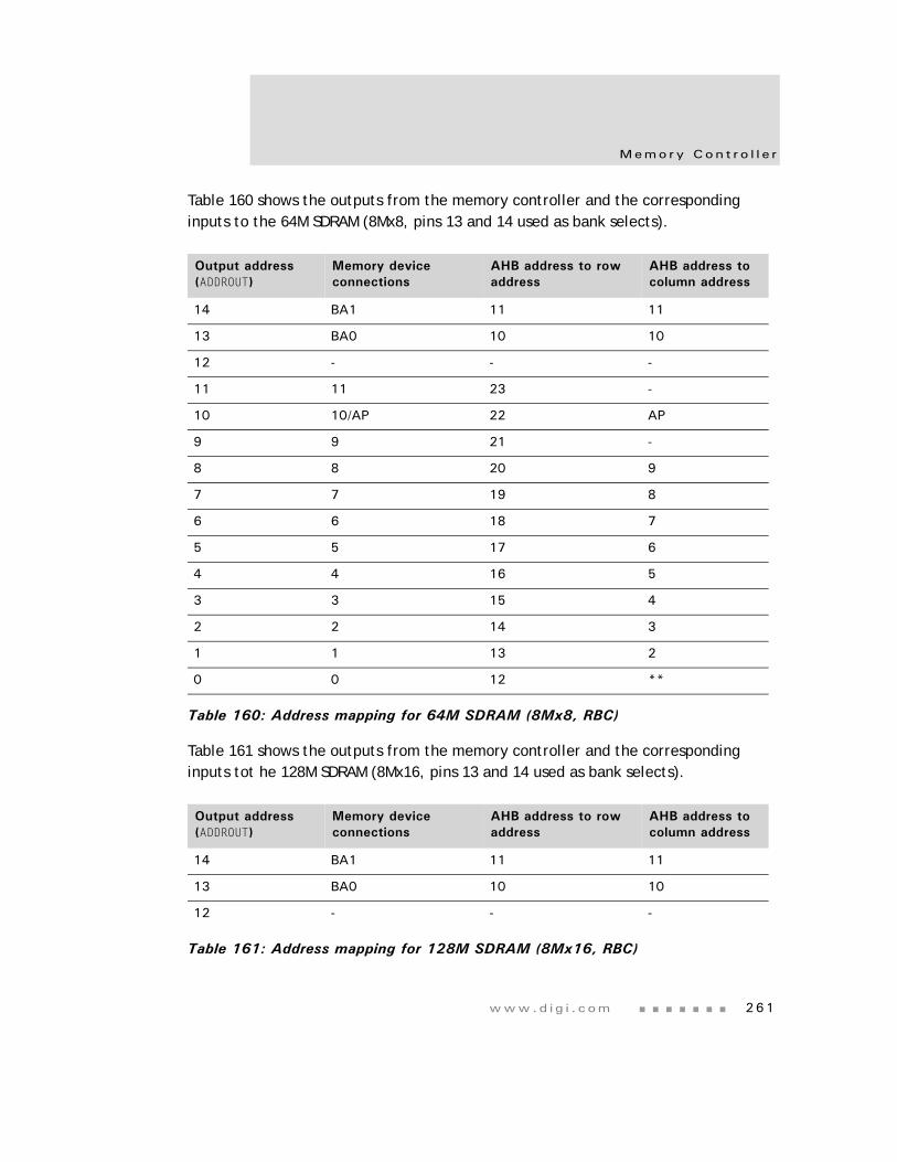
www.d i g i . com 261
Memo ry Con t r o l l e r
Table 160 shows the outputs from the memory controller and the corresponding inputs to the 64M SDRAM (8Mx8, pins 13 and 14 used as bank selects).
Table 161 shows the outputs from the memory controller and the corresponding inputs tot he 128M SDRAM (8Mx16, pins 13 and 14 used as bank selects).
Output address (ADDROUT)
Memory device connections
AHB address to row address
AHB address to column address
14 BA1 11 11
13 BA0 10 10
12 - - -
11 11 23 -
10 10/AP 22 AP
9 9 21 -
8 8 20 9
7 7 19 8
6 6 18 7
5 5 17 6
4 4 16 5
3 3 15 4
2 2 14 3
1 1 13 2
0 0 12 **
Table 160: Address mapping for 64M SDRAM (8Mx8, RBC)
Output address (ADDROUT)
Memory device connections
AHB address to row address
AHB address to column address
14 BA1 11 11
13 BA0 10 10
12 - - -
Table 161: Address mapping for 128M SDRAM (8Mx16, RBC)
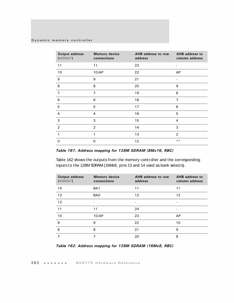
Dynam i c memo ry con t r o l l e r
2 6 2 NS9775 Ha r dwa r e Re f e r ence
Table 162 shows the outputs from the memory controller and the corresponding inputs to the 128M SDRAM (16Mx8, pins 13 and 14 used as bank selects).
11 11 23 -
10 10/AP 22 AP
9 9 21 -
8 8 20 9
7 7 19 8
6 6 18 7
5 5 17 6
4 4 16 5
3 3 15 4
2 2 14 3
1 1 13 2
0 0 12 **
Output address (ADDROUT)
Memory device connections
AHB address to row address
AHB address to column address
14 BA1 11 11
13 BA0 12 12
12 - - -
11 11 24 -
10 10/AP 23 AP
9 9 22 10
8 8 21 9
7 7 20 8
Table 162: Address mapping for 128M SDRAM (16Mx8, RBC)
Output address (ADDROUT)
Memory device connections
AHB address to row address
AHB address to column address
Table 161: Address mapping for 128M SDRAM (8Mx16, RBC)
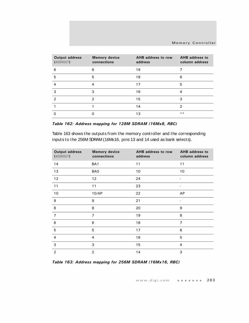
www.d i g i . com 263
Memo ry Con t r o l l e r
Table 163 shows the outputs from the memory controller and the corresponding inputs to the 256M SDRAM (16Mx16, pins 13 and 14 used as bank selects).
6 6 19 7
5 5 18 6
4 4 17 5
3 3 16 4
2 2 15 3
1 1 14 2
0 0 13 **
Output address (ADDROUT)
Memory device connections
AHB address to row address
AHB address to column address
14 BA1 11 11
13 BA0 10 10
12 12 24 -
11 11 23 -
10 10/AP 22 AP
9 9 21 -
8 8 20 9
7 7 19 8
6 6 18 7
5 5 17 6
4 4 16 5
3 3 15 4
2 2 14 3
Table 163: Address mapping for 256M SDRAM (16Mx16, RBC)
Output address (ADDROUT)
Memory device connections
AHB address to row address
AHB address to column address
Table 162: Address mapping for 128M SDRAM (16Mx8, RBC)

Dynam i c memo ry con t r o l l e r
2 6 4 NS9775 Ha r dwa r e Re f e r ence
Table 164 shows the outputs from the memory controller and the corresponding inputs to the 256M SDRAM (32Mx8, pins 13 and 14 used as bank selects).
1 1 13 2
0 0 12 **
Output address (ADDROUT)
Memory device connections
AHB address to row address
AHB address to column address
14 BA1 11 11
13 BA0 12 12
12 12 25 -
11 11 24 -
10 10/AP 23 AP
9 9 22 10
8 8 21 9
7 7 20 8
6 6 19 7
5 5 18 6
4 4 17 5
3 3 16 4
2 2 15 3
1 1 14 2
0 0 13 **
Table 164: Address mapping for 256M SDRAM (32Mx8, RBC)
Output address (ADDROUT)
Memory device connections
AHB address to row address
AHB address to column address
Table 163: Address mapping for 256M SDRAM (16Mx16, RBC)
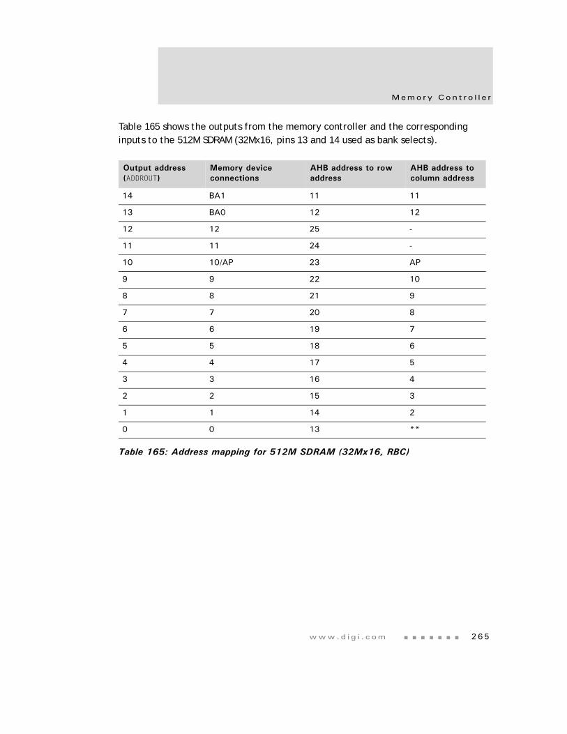
www.d i g i . com 265
Memo ry Con t r o l l e r
Table 165 shows the outputs from the memory controller and the corresponding inputs to the 512M SDRAM (32Mx16, pins 13 and 14 used as bank selects).
Output address (ADDROUT)
Memory device connections
AHB address to row address
AHB address to column address
14 BA1 11 11
13 BA0 12 12
12 12 25 -
11 11 24 -
10 10/AP 23 AP
9 9 22 10
8 8 21 9
7 7 20 8
6 6 19 7
5 5 18 6
4 4 17 5
3 3 16 4
2 2 15 3
1 1 14 2
0 0 13 **
Table 165: Address mapping for 512M SDRAM (32Mx16, RBC)
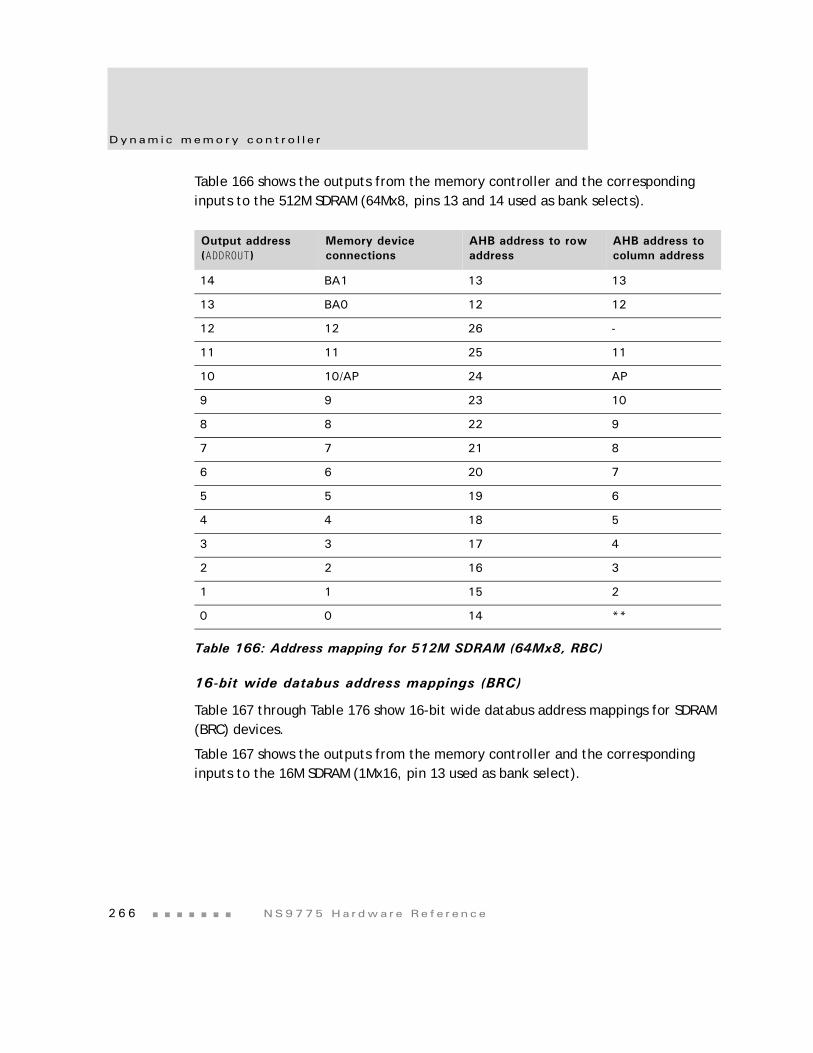
Dynam i c memo ry con t r o l l e r
2 6 6 NS9775 Ha r dwa r e Re f e r ence
Table 166 shows the outputs from the memory controller and the corresponding inputs to the 512M SDRAM (64Mx8, pins 13 and 14 used as bank selects).
16-bit wide databus address mappings (BRC)
Table 167 through Table 176 show 16-bit wide databus address mappings for SDRAM (BRC) devices.
Table 167 shows the outputs from the memory controller and the corresponding inputs to the 16M SDRAM (1Mx16, pin 13 used as bank select).
Output address (ADDROUT)
Memory device connections
AHB address to row address
AHB address to column address
14 BA1 13 13
13 BA0 12 12
12 12 26 -
11 11 25 11
10 10/AP 24 AP
9 9 23 10
8 8 22 9
7 7 21 8
6 6 20 7
5 5 19 6
4 4 18 5
3 3 17 4
2 2 16 3
1 1 15 2
0 0 14 **
Table 166: Address mapping for 512M SDRAM (64Mx8, RBC)
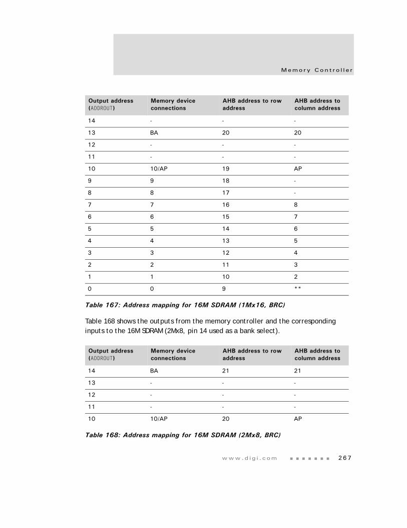
www.d i g i . com 267
Memo ry Con t r o l l e r
Table 168 shows the outputs from the memory controller and the corresponding inputs to the 16M SDRAM (2Mx8, pin 14 used as a bank select).
Output address (ADDROUT)
Memory device connections
AHB address to row address
AHB address to column address
14 - - -
13 BA 20 20
12 - - -
11 - - -
10 10/AP 19 AP
9 9 18 -
8 8 17 -
7 7 16 8
6 6 15 7
5 5 14 6
4 4 13 5
3 3 12 4
2 2 11 3
1 1 10 2
0 0 9 **
Table 167: Address mapping for 16M SDRAM (1Mx16, BRC)
Output address (ADDROUT)
Memory device connections
AHB address to row address
AHB address to column address
14 BA 21 21
13 - - -
12 - - -
11 - - -
10 10/AP 20 AP
Table 168: Address mapping for 16M SDRAM (2Mx8, BRC)
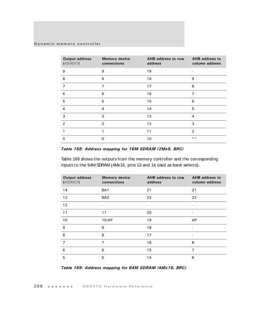
Dynam i c memo ry con t r o l l e r
2 6 8 NS9775 Ha r dwa r e Re f e r ence
Table 169 shows the outputs from the memory controller and the corresponding inputs to the 64M SDRAM (4Mx16, pins 13 and 14 used as bank selects).
9 9 19 -
8 8 18 9
7 7 17 8
6 6 16 7
5 5 15 6
4 4 14 5
3 3 13 4
2 2 12 3
1 1 11 2
0 0 10 **
Output address (ADDROUT)
Memory device connections
AHB address to row address
AHB address to column address
14 BA1 21 21
13 BA0 22 22
12 - - -
11 11 20 -
10 10/AP 19 AP
9 9 18 -
8 8 17 -
7 7 16 8
6 6 15 7
5 5 14 6
Table 169: Address mapping for 64M SDRAM (4Mx16, BRC)
Output address (ADDROUT)
Memory device connections
AHB address to row address
AHB address to column address
Table 168: Address mapping for 16M SDRAM (2Mx8, BRC)
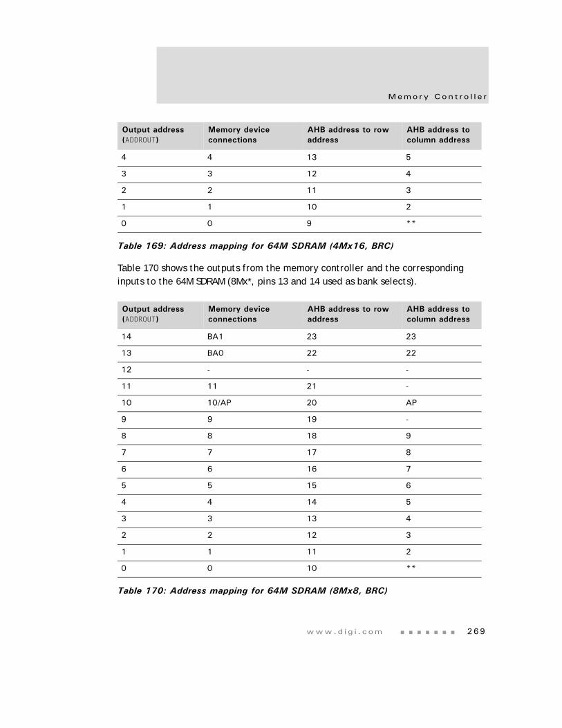
www.d i g i . com 269
Memo ry Con t r o l l e r
Table 170 shows the outputs from the memory controller and the corresponding inputs to the 64M SDRAM (8Mx*, pins 13 and 14 used as bank selects).
4 4 13 5
3 3 12 4
2 2 11 3
1 1 10 2
0 0 9 **
Output address (ADDROUT)
Memory device connections
AHB address to row address
AHB address to column address
14 BA1 23 23
13 BA0 22 22
12 - - -
11 11 21 -
10 10/AP 20 AP
9 9 19 -
8 8 18 9
7 7 17 8
6 6 16 7
5 5 15 6
4 4 14 5
3 3 13 4
2 2 12 3
1 1 11 2
0 0 10 **
Table 170: Address mapping for 64M SDRAM (8Mx8, BRC)
Output address (ADDROUT)
Memory device connections
AHB address to row address
AHB address to column address
Table 169: Address mapping for 64M SDRAM (4Mx16, BRC)
Dynam i c memo ry con t r o l l e r
2 7 0 NS9775 Ha r dwa r e Re f e r ence
Table 171 shows the outputs from the memory controller and the corresponding inputs to the 128M SDRAM (8Mx16, pins 13 and 14 used as bank selects).
Table 172 shows the outputs from the memory controller and the corresponding inputs to the 128 SDRAM (16Mx8, pins 13 and 14 used as bank selects).
Output address (ADDROUT)
Memory device connections
AHB address to row address
AHB address to column address
14 BA1 23 23
13 BA0 22 22
12 - - -
11 11 21 -
10 10/AP 20 AP
9 9 19 -
8 8 18 9
7 7 17 8
6 6 16 7
5 5 15 6
4 4 14 5
3 3 13 4
2 2 12 3
1 1 11 2
0 0 10 **
Table 171: Address mapping for 128M SDRAM (8Mx16, BRC)
Output address (ADDROUT)
Memory device connections
AHB address to row address
AHB address to column address
14 BA1 23 23
13 BA0 24 24
12 - - -
Table 172: Address mapping for 128M SDRAM (16Mx8, BRC)
www.d i g i . com 271
Memo ry Con t r o l l e r
Table 173 shows the outputs for the memory controller and the corresponding inputs to the 256M SDRAM (16Mx16, pins 13 and 14 used as bank selects).
11 11 22 -
10 10/AP 21 AP
9 9 20 10
8 8 19 9
7 7 18 8
6 6 17 7
5 5 16 6
4 4 15 5
3 3 14 4
2 2 13 3
1 1 12 2
0 0 11 **
Output address (ADDROUT)
Memory device connections
AHB address to row address
AHB address to column address
14 BA1 23 23
13 BA0 24 24
12 12 22 -
11 11 21 -
10 10/AP 20 AP
9 9 19 -
8 8 18 9
7 7 17 8
Table 173: Address mapping for 256M SDRAM (16Mx16, BRC)
Output address (ADDROUT)
Memory device connections
AHB address to row address
AHB address to column address
Table 172: Address mapping for 128M SDRAM (16Mx8, BRC)
Dynam i c memo ry con t r o l l e r
2 7 2 NS9775 Ha r dwa r e Re f e r ence
Table 174 shows the outputs for the memory controller and the corresponding inputs to the 256M SDRAM (32Mx8, pins 13 and 14 used as bank selects).
6 6 16 7
5 5 15 6
4 4 14 5
3 3 13 4
2 2 12 3
1 1 11 2
0 0 10 **
Output address (ADDROUT)
Memory device connections
AHB address to row address
AHB address to column address
14 BA1 25 25
13 BA0 24 24
12 12 23 -
11 11 22 -
10 10/AP 21 AP
9 9 20 10
8 8 19 9
7 7 18 8
6 6 17 7
5 5 16 6
4 4 15 5
3 3 14 4
2 2 13 3
Table 174: Address mapping for 256M SDRAM (32Mx8, BRC)
Output address (ADDROUT)
Memory device connections
AHB address to row address
AHB address to column address
Table 173: Address mapping for 256M SDRAM (16Mx16, BRC)
www.d i g i . com 273
Memo ry Con t r o l l e r
Table 175 shows the outputs from the memory controller and the corresponding inputs to the 512M SDRAM (32Mx16, pins 13 and 14 used as bank selects).
1 1 12 2
0 0 11 **
Output address (ADDROUT)
Memory device connections
AHB address to row address
AHB address to column address
14 BA1 25 25
13 BA0 24 24
12 12 23 -
11 11 22 -
10 10/AP 21 AP
9 9 20 10
8 8 19 9
7 7 18 8
6 6 17 7
5 5 16 6
4 4 15 5
3 3 14 4
2 2 13 3
1 1 12 2
0 0 11 **
Table 175: Address mapping for 512M SDRAM (32Mx16, BRC)
Output address (ADDROUT)
Memory device connections
AHB address to row address
AHB address to column address
Table 174: Address mapping for 256M SDRAM (32Mx8, BRC)
Dynam i c memo ry con t r o l l e r
2 7 4 NS9775 Ha r dwa r e Re f e r ence
Table 176 shows the outputs from the memory controller and the corresponding inputs to the 512M SDRAM (64Mx8, pins 13 and 14 used as bank selects).
Output address (ADDROUT)
Memory device connections
AHB address to row address
AHB address to column address
14 BA1 26 26
13 BA0 25 25
12 12 24 -
11 11 23 11
10 10/AP 22 AP
9 9 21 10
8 8 20 9
7 7 19 8
6 6 18 7
5 5 17 6
4 4 16 5
3 3 15 4
2 2 14 3
1 1 13 2
0 0 12 **
Table 176: Address mapping for 512M SDRAM (64Mx8, BRC)
www.d i g i . com 275
Memo ry Con t r o l l e r
Registers
The external memory is accessed using the AHB memory interface ports. Addresses are not fixed, but are determined by the AHB decoder and can be different for any particular system implementation. Transfers to the external memory controller memories are selected by the HSELMPMC[3:0]CS[7:0] signals (where [3:0] indicates the AHB port number and [7:0] indicates the chip select to be accessed.)
Register map
Table 177 lists the registers in the Memory Controller register map. All configuration registers must be accessed as 32-bit words and as single accesses only. No bursting is allowed.
Address Register Description
A070 0000 Control register Control register
A070 0004 Status register Status register
A070 0008 Config register Configuration register
A070 0020 DynamicControl Dynamic Memory Control register
A070 0024 DynamicRefresh Dynamic Memory Refresh Timer
A070 0028 DynamicReadConfig Dynamic Memory Read Configuration register
A070 0030 DynamictRP Dynamic Memory Precharge Command Period (tRP)
A070 0034 DynamictRAS Dynamic Memory Active to Precharge Command Period (tRAS)
A070 0038 DynamictSREX Dynamic Memory Self-Refresh Exit Time (tSREX)
A070 003C DynamictAPR Dynamic Memory Last Data Out to Active Time (tAPR)
A070 0040 DynamictDAL Dynamic Memory Data-in to Active Command Time (tDAL or TAPW)
A070 0044 DynamictWR Dynamic Memory Write Recovery Time (tWR, tDPL, tRWL, tRDL)
Table 177: Memory Controller register map
Reg i s t e r s
2 7 6 NS9775 Ha r dwa r e Re f e r ence
A070 0048 DynamictRC Dynamic Memory Active to Active Command Period (tRC)
A070 004C DynamictRFC Dynamic Memory Auto Refresh Period, and Auto Refresh to Active Command Period (tRFC)
A070 0050 DynamictXSR Dynamic Memory Exit Self-Refresh to Active Command (tXSR)
A070 0054 DynamictRRD Dynamic Memory Active Bank A to Active B Time (tRRD)
A070 0058 DynamictMRD Dynamic Memory Load Mode register to Active Command Time (tMRD)
A070 0080 StaticExtendedWait Static Memory Extended Wait
A070 0100 DynamicConfig0 Dynamic Memory Configuration Register 0
A070 0104 DynamicRasCas0 Dynamic Memory RAS and CAS Delay 0
A070 0120 DynamicConfig1 Dynamic Memory Configuration Register 1
A070 0124 DynamicRasCas1 Dynamic Memory RAS and CAS Delay 1
A070 0140 DynamicConfig2 Dynamic Memory Configuration Register 2
A070 0144 DynamicRasCas2 Dynamic Memory RAS and CAS Delay 2
A070 0160 DynamicConfig3 Dynamic Memory Configuration Register 3
A070 0164 DynamicRasCas3 Dynamic Memory RAS and CAS Delay 3
A070 0200 StaticConfig0 Static Memory Configuration Register 0
A070 0204 StaticWaitWen0 Static Memory Write Enable Delay 0
A070 0208 StaticWaitOen0 Static Memory Output Enable Delay 0
A070 020C StaticWaitRd0 Static Memory Read Delay 0
A070 0210 StaticWaitPage0 Static Memory Page Mode Read Delay 0
A070 0214 StaticWaitWr0 Static Memory Write Delay 0
A070 0218 StaticWaitTurn0 Static Memory Turn Round Delay 0
A070 0220 StaticConfig1 Static Memory Configuration Register 1
A070 0224 StaticWaitWen1 Static Memory Write Enable Delay 1
A070 0228 StaticWaitOen1 Static Memory Output Enable Delay 1
Address Register Description
Table 177: Memory Controller register map
www.d i g i . com 277
Memo ry Con t r o l l e r
Reset values
Reset values will be noted as appropriate in the Description column of each register table, rather than as a separate column.
A070 022C StaticWaitRd1 Static Memory Read Delay 1
A070 0230 StaticWaitPage1 Static Memory Page Mode Read Delay 1
A070 0234 StaticWaitWr1 Static Memory Write Delay 1
A070 0238 StaticWaitTurn1 Static Memory Turn Round Delay 1
A070 0240 StaticConfig2 Static Memory Configuration Register 2
A070 0244 StaticWaitWen2 Static Memory Write Enable Delay 2
A070 0248 StaticWaitOen2 Static Memory Output Enable Delay 2
A070 024C StaticWaitRd2 Static Memory Read Delay 2
A070 0250 StaticWaitPage2 Static Memory Page Mode Read Delay 2
A070 0254 StaticWaitWr2 Static Memory Write Delay 2
A070 0258 StaticWaitTurn2 Static Memory Turn Round Delay 2
A070 0260 StaticConfig3 Static Memory Configuration Register 3
A070 0264 StaticWaitWen3 Static Memory Write Enable Delay 3
A070 0268 StaticWaitOen3 Static Memory Output Enable Delay 3
A070 026C StaticWaitRd3 Static memory Read Delay 3
A070 0270 StaticWaitPage3 Static Memory Page Mode Read Delay 3
A070 0274 StaticWaitWr3 Static Memory Write Delay 3
A070 0278 StaticWaitTurn3 Static Memory Turn Round Delay 3
Address Register Description
Table 177: Memory Controller register map
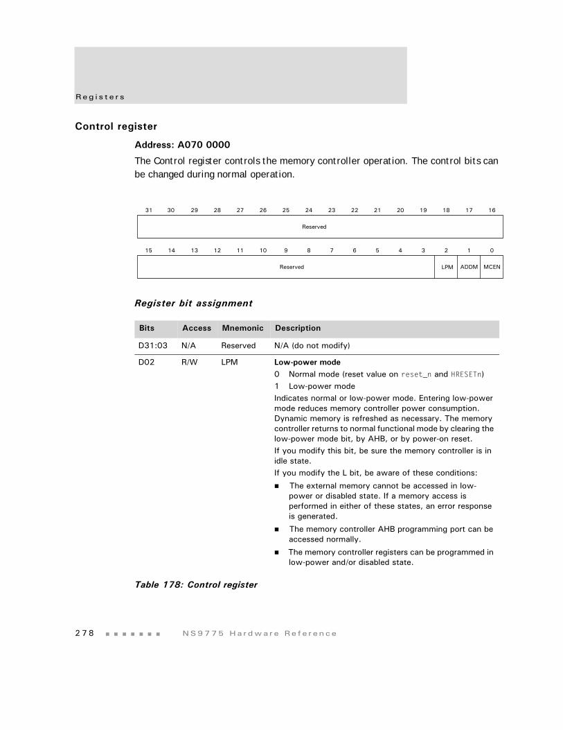
Reg i s t e r s
2 7 8 NS9775 Ha r dwa r e Re f e r ence
Control register
Address: A070 0000
The Control register controls the memory controller operation. The control bits can be changed during normal operation.
Register bit assignment
Bits Access Mnemonic Description
D31:03 N/A Reserved N/A (do not modify)
D02 R/W LPM Low-power mode0 Normal mode (reset value on reset_n and HRESETn)1 Low-power modeIndicates normal or low-power mode. Entering low-power mode reduces memory controller power consumption. Dynamic memory is refreshed as necessary. The memory controller returns to normal functional mode by clearing the low-power mode bit, by AHB, or by power-on reset.If you modify this bit, be sure the memory controller is in idle state. If you modify the L bit, be aware of these conditions:
The external memory cannot be accessed in low-power or disabled state. If a memory access is performed in either of these states, an error response is generated.
The memory controller AHB programming port can be accessed normally.
The memory controller registers can be programmed in low-power and/or disabled state.
Table 178: Control register
MCEN
13 12 11 10 9 8 7 6 5 4 3 2 1 015 14
31 29 28 27 26 25 24 23 22 21 20 19 18 17 1630
Reserved
Reserved LPM ADDM
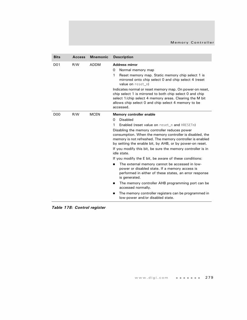
www.d i g i . com 279
Memo ry Con t r o l l e r
D01 R/W ADDM Address mirror0 Normal memory map1 Reset memory map. Static memory chip select 1 is
mirrored onto chip select 0 and chip select 4 (reset value on reset_n)
Indicates normal or reset memory map. On power-on reset, chip select 1 is mirrored to both chip select 0 and chip select 1/chip select 4 memory areas. Clearing the M bit allows chip select 0 and chip select 4 memory to be accessed.
D00 R/W MCEN Memory controller enable0 Disabled1 Enabled (reset value on reset_n and HRESETn)Disabling the memory controller reduces power consumption. When the memory controller is disabled, the memory is not refreshed. The memory controller is enabled by setting the enable bit, by AHB, or by power-on reset.If you modify this bit, be sure the memory controller is in idle state. If you modify the E bit, be aware of these conditions:
The external memory cannot be accessed in low-power or disabled state. If a memory access is performed in either of these states, an error response is generated.
The memory controller AHB programming port can be accessed normally.
The memory controller registers can be programmed in low-power and/or disabled state.
Bits Access Mnemonic Description
Table 178: Control register
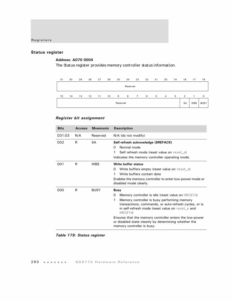
Reg i s t e r s
2 8 0 NS9775 Ha r dwa r e Re f e r ence
Status register
Address: A070 0004The Status register provides memory controller status information.
Register bit assignment
Bits Access Mnemonic Description
D31:03 N/A Reserved N/A (do not modify)
D02 R SA Self-refresh acknowledge (SREFACK)0 Normal mode1 Self refresh mode (reset value on reset_n)Indicates the memory controller operating mode.
D01 R WBS Write buffer status0 Write buffers empty (reset value on reset_n)1 Write buffers contain dataEnables the memory controller to enter low-power mode or disabled mode clearly.
D00 R BUSY Busy0 Memory controller is idle (reset value on HRESETn)1 Memory controller is busy performing memory
transactions, commands, or auto-refresh cycles, or is in self-refresh mode (reset value on reset_n and HRESETn)
Ensures that the memory controller enters the low-power or disabled state cleanly by determining whether the memory controller is busy.
Table 179: Status register
BUSY
13 12 11 10 9 8 7 6 5 4 3 2 1 015 14
31 29 28 27 26 25 24 23 22 21 20 19 18 17 1630
Reserved
Reserved SA WBS
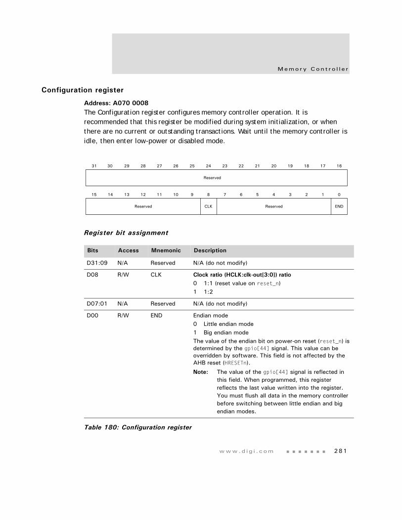
www.d i g i . com 281
Memo ry Con t r o l l e r
Configuration register
Address: A070 0008The Configuration register configures memory controller operation. It is recommended that this register be modified during system initialization, or when there are no current or outstanding transactions. Wait until the memory controller is idle, then enter low-power or disabled mode.
Register bit assignment
Bits Access Mnemonic Description
D31:09 N/A Reserved N/A (do not modify)
D08 R/W CLK Clock ratio (HCLK:clk-out[3:0]) ratio0 1:1 (reset value on reset_n)1 1:2
D07:01 N/A Reserved N/A (do not modify)
D00 R/W END Endian mode0 Little endian mode1 Big endian modeThe value of the endian bit on power-on reset (reset_n) is determined by the gpio[44] signal. This value can be overridden by software. This field is not affected by the AHB reset (HRESETn).
Note: The value of the gpio[44] signal is reflected in this field. When programmed, this register reflects the last value written into the register. You must flush all data in the memory controller before switching between little endian and big endian modes.
Table 180: Configuration register
END
13 12 11 10 9 8 7 6 5 4 3 2 1 015 14
31 29 28 27 26 25 24 23 22 21 20 19 18 17 1630
Reserved
Reserved CLK Reserved
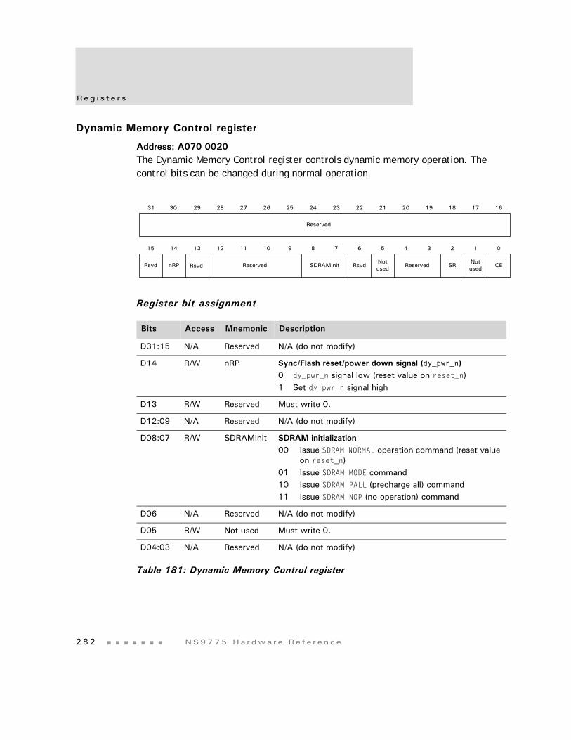
Reg i s t e r s
2 8 2 NS9775 Ha r dwa r e Re f e r ence
Dynamic Memory Control register
Address: A070 0020The Dynamic Memory Control register controls dynamic memory operation. The control bits can be changed during normal operation.
Register bit assignment
Bits Access Mnemonic Description
D31:15 N/A Reserved N/A (do not modify)
D14 R/W nRP Sync/Flash reset/power down signal (dy_pwr_n)0 dy_pwr_n signal low (reset value on reset_n)1 Set dy_pwr_n signal high
D13 R/W Reserved Must write 0.
D12:09 N/A Reserved N/A (do not modify)
D08:07 R/W SDRAMInit SDRAM initialization00 Issue SDRAM NORMAL operation command (reset value
on reset_n)01 Issue SDRAM MODE command10 Issue SDRAM PALL (precharge all) command11 Issue SDRAM NOP (no operation) command
D06 N/A Reserved N/A (do not modify)
D05 R/W Not used Must write 0.
D04:03 N/A Reserved N/A (do not modify)
Table 181: Dynamic Memory Control register
CE
13 12 11 10 9 8 7 6 5 4 3 2 1 015 14
31 29 28 27 26 25 24 23 22 21 20 19 18 17 1630
Reserved
SDRAMInit ReservedRsvd nRP Reserved SR Not usedRsvd Not
usedRsvd
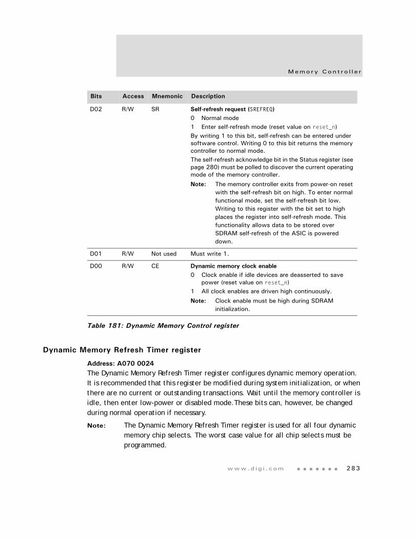
www.d i g i . com 283
Memo ry Con t r o l l e r
Dynamic Memory Refresh Timer register
Address: A070 0024The Dynamic Memory Refresh Timer register configures dynamic memory operation. It is recommended that this register be modified during system initialization, or when there are no current or outstanding transactions. Wait until the memory controller is idle, then enter low-power or disabled mode.These bits can, however, be changed during normal operation if necessary.
Note: The Dynamic Memory Refresh Timer register is used for all four dynamic memory chip selects. The worst case value for all chip selects must be programmed.
D02 R/W SR Self-refresh request (SREFREQ)0 Normal mode1 Enter self-refresh mode (reset value on reset_n)By writing 1 to this bit, self-refresh can be entered under software control. Writing 0 to this bit returns the memory controller to normal mode.The self-refresh acknowledge bit in the Status register (see page 280) must be polled to discover the current operating mode of the memory controller.
Note: The memory controller exits from power-on reset with the self-refresh bit on high. To enter normal functional mode, set the self-refresh bit low. Writing to this register with the bit set to high places the register into self-refresh mode. This functionality allows data to be stored over SDRAM self-refresh of the ASIC is powered down.
D01 R/W Not used Must write 1.
D00 R/W CE Dynamic memory clock enable0 Clock enable if idle devices are deasserted to save
power (reset value on reset_n)1 All clock enables are driven high continuously.
Note: Clock enable must be high during SDRAM initialization.
Bits Access Mnemonic Description
Table 181: Dynamic Memory Control register
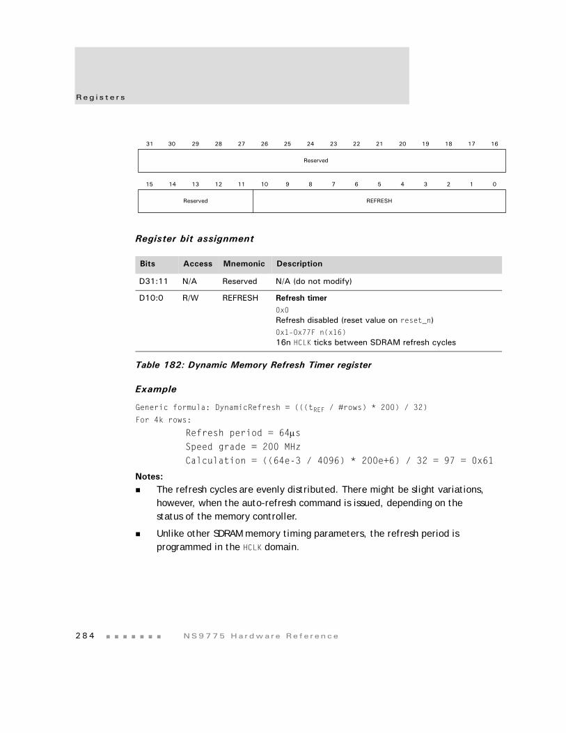
Reg i s t e r s
2 8 4 NS9775 Ha r dwa r e Re f e r ence
Register bit assignment
Example
Generic formula: DynamicRefresh = (((tREF / #rows) * 200) / 32)
For 4k rows:
Refresh period = 64μsSpeed grade = 200 MHz
Calculation = ((64e-3 / 4096) * 200e+6) / 32 = 97 = 0x61
Notes:The refresh cycles are evenly distributed. There might be slight variations, however, when the auto-refresh command is issued, depending on the status of the memory controller.
Unlike other SDRAM memory timing parameters, the refresh period is programmed in the HCLK domain.
Bits Access Mnemonic Description
D31:11 N/A Reserved N/A (do not modify)
D10:0 R/W REFRESH Refresh timer0x0Refresh disabled (reset value on reset_n)0x1–0x77F n(x16)16n HCLK ticks between SDRAM refresh cycles
Table 182: Dynamic Memory Refresh Timer register
13 12 11 10 9 8 7 6 5 4 3 2 1 015 14
31 29 28 27 26 25 24 23 22 21 20 19 18 17 1630
Reserved
REFRESHReserved
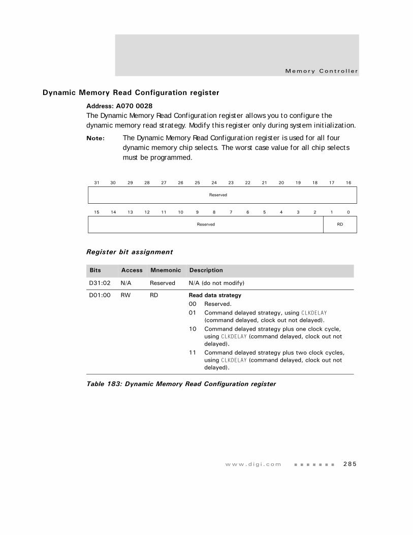
www.d i g i . com 285
Memo ry Con t r o l l e r
Dynamic Memory Read Configuration register
Address: A070 0028The Dynamic Memory Read Configuration register allows you to configure the dynamic memory read strategy. Modify this register only during system initialization.
Note: The Dynamic Memory Read Configuration register is used for all four dynamic memory chip selects. The worst case value for all chip selects must be programmed.
Register bit assignment
Bits Access Mnemonic Description
D31:02 N/A Reserved N/A (do not modify)
D01:00 RW RD Read data strategy00 Reserved.01 Command delayed strategy, using CLKDELAY
(command delayed, clock out not delayed).10 Command delayed strategy plus one clock cycle,
using CLKDELAY (command delayed, clock out not delayed).
11 Command delayed strategy plus two clock cycles, using CLKDELAY (command delayed, clock out not delayed).
Table 183: Dynamic Memory Read Configuration register
13 12 11 10 9 8 7 6 5 4 3 2 1 015 14
31 29 28 27 26 25 24 23 22 21 20 19 18 17 1630
Reserved
Reserved RD
Reg i s t e r s
2 8 6 NS9775 Ha r dwa r e Re f e r ence
Dynamic Memory Precharge Command Period register
Address: A070 0030The Dynamic Memory Precharge Command Period register allows you to program the precharge command period, tRP. Modify this register only during system initialization. This value normally is found in SDRAM datasheets as tRP.
Note: The Dynamic Memory Precharge Command Period register is used for all four dynamic memory chip selects. The worst case value for all chip selects must be programmed.
Register bit assignment
Bits Access Mnemonic Description
D31:04 N/A Reserved N/A (do not modify)
D03:00 R/W RP Precharge command period (tRP)0x0–0xEn+1 clock cycles, where the delay is in CLK cycles.0xF16 clock cycles (reset value on reset_n)
Table 184: Dynamic Memory Precharge Command Period register
13 12 11 10 9 8 7 6 5 4 3 2 1 015 14
31 29 28 27 26 25 24 23 22 21 20 19 18 17 1630
Reserved
Reserved RP
www.d i g i . com 287
Memo ry Con t r o l l e r
Dynamic Memory Active to Precharge Command Period register
Address: A070 0034The Dynamic Memory Active to Precharge Command Period register allows you to program the active to precharge command period, tRAS. It is recommended that this register be modified during system initialization, or when there are no current or outstanding transactions. Wait until the memory controller is idle, then enter low-power or disabled mode. This value normally is found in SDRAM datasheets as tRAS.
Note: The Dynamic Memory Active to Precharge Command Period register is used for all four dynamic memory chip selects. The worst case value for all chip selects must be programmed.
Register bit assignment
Bits Access Mnemonic Description
D31:04 N/A Reserved N/A (do not modify)
D03:00 R/W RAS Active to precharge command period (tRAS)0x0–0xEn+1 clock cycles, where the delay is in CLK cycles.0xF16 clock cycles (reset value on reset_n)
Table 185: Dynamic Memory Active to Precharge Command Period register
13 12 11 10 9 8 7 6 5 4 3 2 1 015 14
31 29 28 27 26 25 24 23 22 21 20 19 18 17 1630
Reserved
Reserved RAS
Reg i s t e r s
2 8 8 NS9775 Ha r dwa r e Re f e r ence
Dynamic Memory Self-refresh Exit Time register
Address: A070 0038The Dynamic Memory Self-refresh Exit Time register allows you to program the self-refresh exit time, tSREX. It is recommended that this register be modified during system initialization, or when there are no current or outstanding transactions. Wait until the memory controller is idle, then enter low-power or disabled mode. This value normally is found in SDRAM data sheets as tSREX.
Note: The Dynamic Memory Self-refresh Exit Time register is used for all four dynamic memory chip selects. The worst case value for all chip selects must be programmed.
Register bit assignment
Bits Access Mnemonic Description
D31:04 N/A Reserved N/A (do not modify)
D03:00 R/W SREX Self-refresh exit time (tSREX)0x0–0xEn+1 clock cycles, where the delay is in CLK cycles.0xF16 clock cycles (reset value on reset_n)
Table 186: Dynamic Memory Self-refresh Exit Time register
13 12 11 10 9 8 7 6 5 4 3 2 1 015 14
31 29 28 27 26 25 24 23 22 21 20 19 18 17 1630
Reserved
Reserved SREX
www.d i g i . com 289
Memo ry Con t r o l l e r
Dynamic Memory Last Data Out to Active Time register
Address: A070 003CThe Dynamic Memory Last Data Out to Active Time register allows you to program the last-data-out to active command time, tAPR. It is recommended that this register be modified during system initialization, or when there are no current or outstanding transactions. Wait until the memory controller is idle, then enter low-power or disabled mode. This value normally is found in SDRAM datasheets as tAPR.
Note: The Dynamic Memory Last Data Out to Active Time register is used for all four dynamic memory chip selects. The worst case value for all chip selects must be programmed.
Register bit assignment
Bits Access Mnemonic Description
D31:04 N/A Reserved N/A (do not modify)
D03:00 R/W APR Last-data-out to active command time (tAPR)0x0–0xEn+1 clock cycles, where the delay is in CLK cycles.0xF16 clock cycles (reset value on reset_n)
Table 187: Dynamic Memory Last Data Out to Active Time register
13 12 11 10 9 8 7 6 5 4 3 2 1 015 14
31 29 28 27 26 25 24 23 22 21 20 19 18 17 1630
Reserved
Reserved APR
Reg i s t e r s
2 9 0 NS9775 Ha r dwa r e Re f e r ence
Dynamic Memory Data-in to Active Command Time register
Address: A070 0040The Dynamic Memory Data-in to Active Command Time register allows you to program the data-in to active command time, tDAL. It is recommended that this register be modified during system initialization, or when there are no current or outstanding transactions. Wait until the memory controller is idle, then enter low-power or disabled mode. This value normally is found in SDRAM data sheets as tDAL or tAPW.
Note: The Dynamic Memory Data-in Active Command Time register is used for all four dynamic memory chip selects. The worst case value for all chip selects must be programmed.
Register bit assignment
Bits Access Mnemonic Description
D31:04 N/A Reserved N/A (do not modify)
D03:00 R/W DAL Data-in to active command (tDAL or tAPW)0x0–0xEn+1 clock cycles, where the delay is in CLK cycles.0xF15 clock cycles (reset value on reset_n)
Table 188: Dynamic Memory Data-in Active Command Time register
13 12 11 10 9 8 7 6 5 4 3 2 1 015 14
31 29 28 27 26 25 24 23 22 21 20 19 18 17 1630
Reserved
Reserved DAL
www.d i g i . com 291
Memo ry Con t r o l l e r
Dynamic Memory Write Recovery Time register
Address: A070 0044The Dynamic Memory Write Recovery Time register allows you to program the write recovery time, tWR. It is recommended that this register be modified during system initialization, or when there are no current or outstanding transactions. Wait until the memory controller is idle, then enter low-power or disabled mode. This value normally is found in SDRAM datasheets as tWR, tDPL, tRWL, or tRDL.
Note: The Dynamic Memory Write Recovery Time register is used for all four dynamic memory chip selects. The worst case value for all chip selects must be programmed.
Register bit assignment
Bits Access Mnemonic Description
D31:04 N/A Reserved N/A (do not modify)
D03:00 R/W WR Write recovery time (tWR, tDPL, tRWL, or tRDL)0x0–0xEn+1 clock cycles, where the delay is in CLK cycles.0xF16 clock cycles (reset value on reset_n)
Table 189: Dynamic Memory Write Recovery TIme register
13 12 11 10 9 8 7 6 5 4 3 2 1 015 14
31 29 28 27 26 25 24 23 22 21 20 19 18 17 1630
Reserved
Reserved WR
Reg i s t e r s
2 9 2 NS9775 Ha r dwa r e Re f e r ence
Dynamic Memory Active to Active Command Period register
Address: A070 0048The Dynamic Memory Active to Active Command Period register allows you to program the active to active command period, tRC. It is recommended that this register be modified during system initialization, or when there are no current or outstanding transactions. Wait until the memory controller is idle, then enter low-power or disabled mode. This value normally is found in SDRAM datasheets as tRC.
Note: The Dynamic Memory Active to Active Command period register is used for all four dynamic memory chip selects. The worst case value for all chip selects must be programmed.
Register bit assignment
Bits Access Mnemonic Description
D31:05 N/A Reserved N/A (do not modify)
D04:00 R/W RC Active to active command period (tRC)0x0–0x1En+1 clock cycles, where the delay is in CLK cycles.0x1F32 clock cycles (reset value on reset_n)
Table 190: Dynamic Memory Active to Active Command Period register
13 12 11 10 9 8 7 6 5 4 3 2 1 015 14
31 29 28 27 26 25 24 23 22 21 20 19 18 17 1630
Reserved
Reserved RC
www.d i g i . com 293
Memo ry Con t r o l l e r
Dynamic Memory Auto Refresh Period register
Address: A070 004CThe Dynamic Memory Auto Refresh Period register allows you to program the auto-refresh period and the auto-refresh to active command period, tRFC. It is recommended that this register be modified during initialization, or when there are no current or outstanding transactions. Wait until the memory controller is idle, then enter low-power or disabled mode. This value normally is found in SDRAM datasheets as tRFC or tRC.
Note: The Dynamic Memory Auto Refresh Period register is used for all four dynamic memory chip selects. The worst case value for all chip selects must be programmed.
Register bit assignment
Bits Access Mnemonic Description
D31:05 N/A Reserved N/A (do not modify)
D04:00 R/W RFC Auto-refresh period and auto-refresh to active command period0x0–0x1En+1 clock cycles, where the delay is in CLK cycles.0x1F32 clock cycles (reset value on reset_n)
Table 191: Dynamic Memory Auto Refresh Period register
13 12 11 10 9 8 7 6 5 4 3 2 1 015 14
31 29 28 27 26 25 24 23 22 21 20 19 18 17 1630
Reserved
Reserved RFC
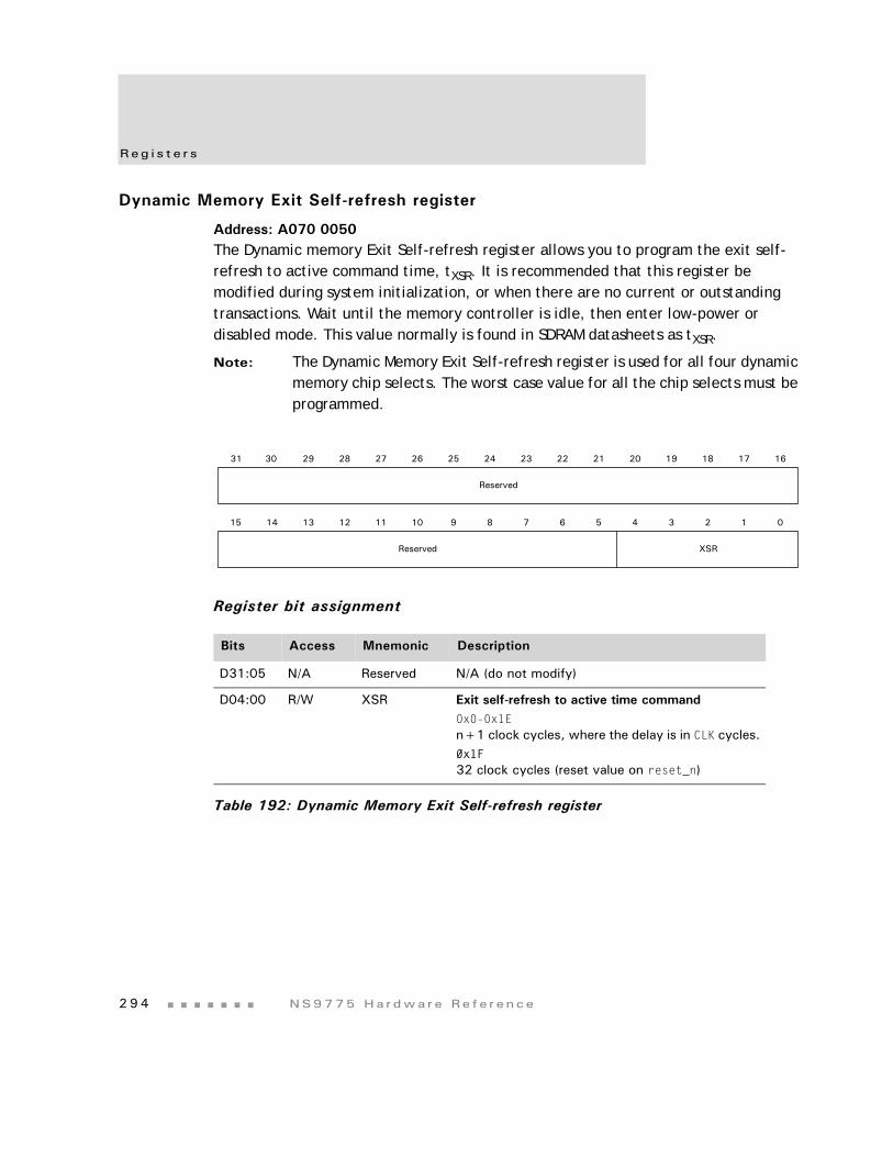
Reg i s t e r s
2 9 4 NS9775 Ha r dwa r e Re f e r ence
Dynamic Memory Exit Self-refresh register
Address: A070 0050The Dynamic memory Exit Self-refresh register allows you to program the exit self-refresh to active command time, tXSR. It is recommended that this register be modified during system initialization, or when there are no current or outstanding transactions. Wait until the memory controller is idle, then enter low-power or disabled mode. This value normally is found in SDRAM datasheets as tXSR.
Note: The Dynamic Memory Exit Self-refresh register is used for all four dynamic memory chip selects. The worst case value for all the chip selects must be programmed.
Register bit assignment
Bits Access Mnemonic Description
D31:05 N/A Reserved N/A (do not modify)
D04:00 R/W XSR Exit self-refresh to active time command0x0–0x1En+1 clock cycles, where the delay is in CLK cycles.0x1F32 clock cycles (reset value on reset_n)
Table 192: Dynamic Memory Exit Self-refresh register
13 12 11 10 9 8 7 6 5 4 3 2 1 015 14
31 29 28 27 26 25 24 23 22 21 20 19 18 17 1630
Reserved
Reserved XSR
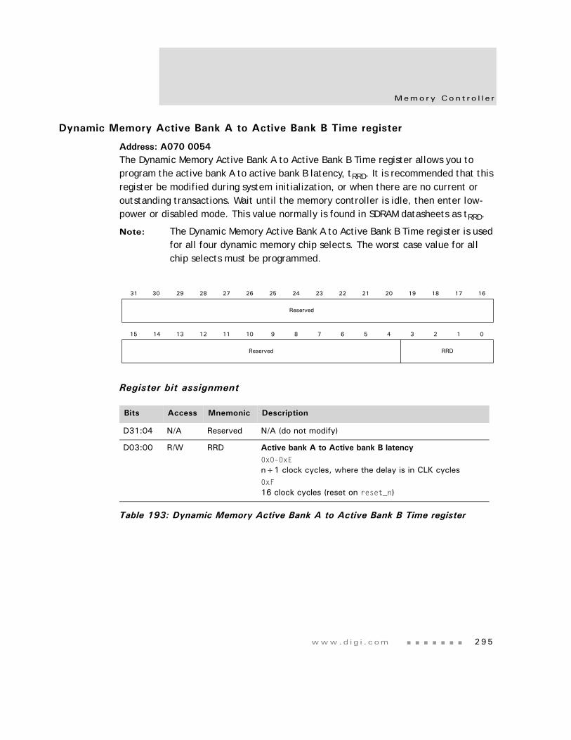
www.d i g i . com 295
Memo ry Con t r o l l e r
Dynamic Memory Active Bank A to Active Bank B Time register
Address: A070 0054The Dynamic Memory Active Bank A to Active Bank B Time register allows you to program the active bank A to active bank B latency, tRRD. It is recommended that this register be modified during system initialization, or when there are no current or outstanding transactions. Wait until the memory controller is idle, then enter low-power or disabled mode. This value normally is found in SDRAM datasheets as tRRD.
Note: The Dynamic Memory Active Bank A to Active Bank B Time register is used for all four dynamic memory chip selects. The worst case value for all chip selects must be programmed.
Register bit assignment
Bits Access Mnemonic Description
D31:04 N/A Reserved N/A (do not modify)
D03:00 R/W RRD Active bank A to Active bank B latency0x0–0xEn+1 clock cycles, where the delay is in CLK cycles0xF16 clock cycles (reset on reset_n)
Table 193: Dynamic Memory Active Bank A to Active Bank B Time register
13 12 11 10 9 8 7 6 5 4 3 2 1 015 14
31 29 28 27 26 25 24 23 22 21 20 19 18 17 1630
Reserved
Reserved RRD
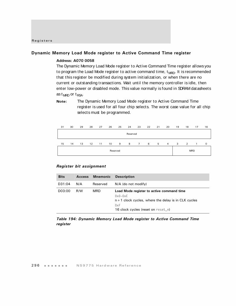
Reg i s t e r s
2 9 6 NS9775 Ha r dwa r e Re f e r ence
Dynamic Memory Load Mode register to Active Command Time register
Address: A070 0058The Dynamic Memory Load Mode register to Active Command Time register allows you to program the Load Mode register to active command time, tMRD. It is recommended that this register be modified during system initialization, or when there are no current or outstanding transactions. Wait until the memory controller is idle, then enter low-power or disabled mode. This value normally is found in SDRAM datasheets as tMRD or tRSA.
Note: The Dynamic Memory Load Mode register to Active Command Time register is used for all four chip selects. The worst case value for all chip selects must be programmed.
Register bit assignment
Bits Access Mnemonic Description
D31:04 N/A Reserved N/A (do not modify)
D03:00 R/W MRD Load Mode register to active command time0x0–0xEn+1 clock cycles, where the delay is in CLK cycles0xF16 clock cycles (reset on reset_n)
Table 194: Dynamic Memory Load Mode register to Active Command Time register
13 12 11 10 9 8 7 6 5 4 3 2 1 015 14
31 29 28 27 26 25 24 23 22 21 20 19 18 17 1630
Reserved
Reserved MRD
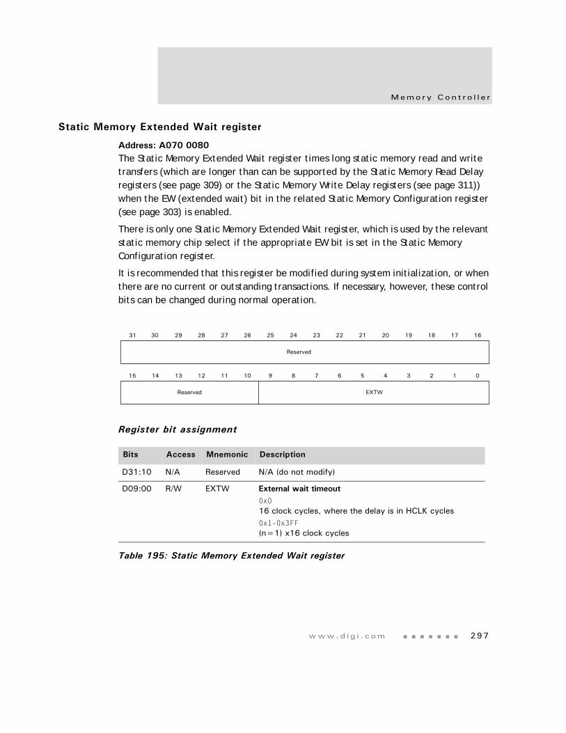
www.d i g i . com 297
Memo ry Con t r o l l e r
Static Memory Extended Wait register
Address: A070 0080The Static Memory Extended Wait register times long static memory read and write transfers (which are longer than can be supported by the Static Memory Read Delay registers (see page 309) or the Static Memory Write Delay registers (see page 311)) when the EW (extended wait) bit in the related Static Memory Configuration register (see page 303) is enabled.
There is only one Static Memory Extended Wait register, which is used by the relevant static memory chip select if the appropriate EW bit is set in the Static Memory Configuration register.
It is recommended that this register be modified during system initialization, or when there are no current or outstanding transactions. If necessary, however, these control bits can be changed during normal operation.
Register bit assignment
Bits Access Mnemonic Description
D31:10 N/A Reserved N/A (do not modify)
D09:00 R/W EXTW External wait timeout0x016 clock cycles, where the delay is in HCLK cycles0x1–0x3FF(n=1) x16 clock cycles
Table 195: Static Memory Extended Wait register
13 12 11 10 9 8 7 6 5 4 3 2 1 015 14
31 29 28 27 26 25 24 23 22 21 20 19 18 17 1630
Reserved
Reserved EXTW
Reg i s t e r s
2 9 8 NS9775 Ha r dwa r e Re f e r ence
ExampleStatic memory read/write time = 16 ms
CLK frequency = 50 MHz
This value must be programmed into the Static Memory Extended Wait register:
(16 x 10-6 x 50 x 106 / 16) - 1 = 49
Dynamic Memory Configuration 0–3 registers
Address: A070 0100 / 0120 / 0140 / 0160The Dynamic Memory Configuration 0–3 registers allow you to program the configuration information for the relevant dynamic memory chip select. These registers are usually modified only during system initialization.
Register bit assignment
Bits Access Mnemonic Description
D31:21 N/A Reserved N/A (do not modify)
D20 R/W Protect Write protect0 Writes not protected (reset value on reset_n)1 Write protected
D19 R/W BDMC Buffer enable0 Buffer disabled for accesses to this chip select (reset
value on reset_n)1 Buffer enabled for accesses to this chip select. The
buffers must be disabled during SDRAM initialization. The buffers must be enabled during normal operation.
D18:15 N/A Reserved N/A (do not modify)
Table 196: Dynamic Memory Configuration 0–3 registers
Rsvd
13 12 11 10 9 8 7 6 5 4 3 2 1 015 14
Rsvd AM
31 29 28 27 26 25 24 23 22 21 20 19 18 17 1630
Reserved Protect BDMC Reserved
AM1 Reserved MD Reserved
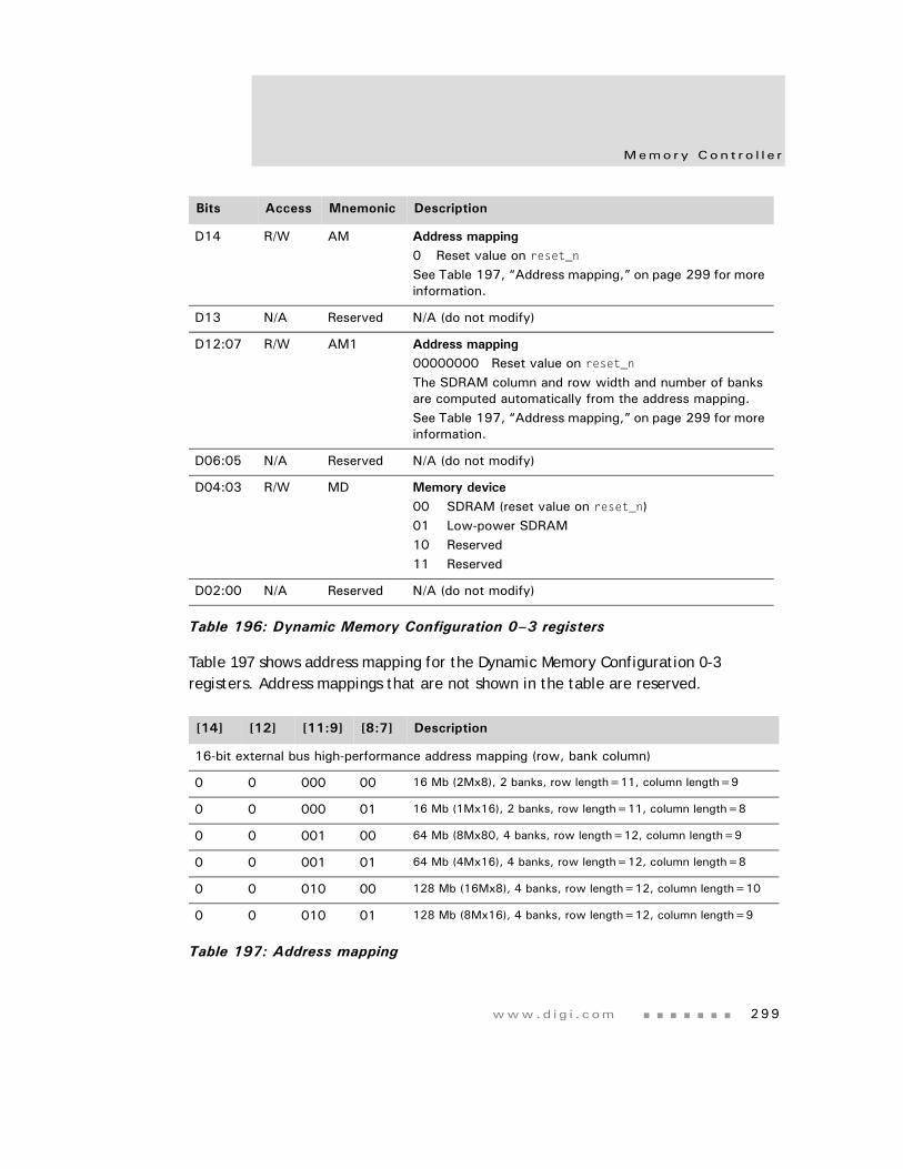
www.d i g i . com 299
Memo ry Con t r o l l e r
Table 197 shows address mapping for the Dynamic Memory Configuration 0-3 registers. Address mappings that are not shown in the table are reserved.
D14 R/W AM Address mapping0 Reset value on reset_nSee Table 197, “Address mapping,” on page 299 for more information.
D13 N/A Reserved N/A (do not modify)
D12:07 R/W AM1 Address mapping00000000 Reset value on reset_nThe SDRAM column and row width and number of banks are computed automatically from the address mapping.See Table 197, “Address mapping,” on page 299 for more information.
D06:05 N/A Reserved N/A (do not modify)
D04:03 R/W MD Memory device00 SDRAM (reset value on reset_n)01 Low-power SDRAM10 Reserved11 Reserved
D02:00 N/A Reserved N/A (do not modify)
[14] [12] [11:9] [8:7] Description
16-bit external bus high-performance address mapping (row, bank column)
0 0 000 00 16 Mb (2Mx8), 2 banks, row length=11, column length=9
0 0 000 01 16 Mb (1Mx16), 2 banks, row length=11, column length=8
0 0 001 00 64 Mb (8Mx80, 4 banks, row length=12, column length=9
0 0 001 01 64 Mb (4Mx16), 4 banks, row length=12, column length=8
0 0 010 00 128 Mb (16Mx8), 4 banks, row length=12, column length=10
0 0 010 01 128 Mb (8Mx16), 4 banks, row length=12, column length=9
Table 197: Address mapping
Bits Access Mnemonic Description
Table 196: Dynamic Memory Configuration 0–3 registers
Reg i s t e r s
3 0 0 NS9775 Ha r dwa r e Re f e r ence
0 0 011 00 256 Mb (32Mx8), 4 banks, row length=13, column length=10
0 0 011 01 256 Mb (16Mx16), 4 banks, row length=13, column length=9
0 0 100 00 512 Mb (64Mx8), 4 banks, row length=13, column length=11
0 0 100 01 512 Mb (32Mx16), 4 banks, row length=13, column length=10
16-bit external bus low-power SDRAM address mapping (bank, row, column)
0 1 000 00 16 Mb (2Mx8), 2 banks, row length=11, column length=9
0 1 000 01 16 Mb (1Mx16), 2 banks, row length=11, column length=8
0 1 001 00 64 Mb (8Mx8), 4 banks, row length 12, column length=9
0 1 001 01 64 Mb (4Mx16), 4 banks, row length=12, column length=8
0 1 010 00 128 Mb (16Mx8), 4 banks, row length=12, column length=10
0 1 010 01 128 Mb (8Mx16), 4 banks, row length=12, column length=9
0 1 011 00 256 Mb (32Mx8), 4 banks, row length=13, column length=10
0 1 011 01 256 Mb (16Mx16), 4 banks, row length=13, column length=9
0 1 100 00 512 Mb (64Mx8), 4 banks, row length=13, column length=11
0 1 100 01 512 Mb (32Mx16, 4 banks, row length=13, column length=10
32-bit extended bus high-performance address mapping (row, bank, column)
1 0 000 00 16 Mb (2Mx8), 2 banks, row length=11, column length=9
1 0 000 01 16 Mb (1Mx16), 2 banks, row length=11, column length=8
1 0 001 00 64 Mb (8Mx8), 4 banks, row length=12, column length=9
1 0 001 01 64 Mb (4Mx16), 4 banks, row length=12, column length=8
1 0 001 10 64 Mb (2Mx32), 4 banks, row length=11, column length=8
1 0 010 00 128 Mb (16Mx8), 4 banks, row length=12, column length=10
1 0 010 01 128 Mb (8Mx16), 4 banks, row length=12, column length=9
1 0 010 10 128 Mb (4Mx32), 4 banks, row length=12, column length=8
1 0 011 00 256 Mb (32Mx8), 4 banks, row length=13, column length=10
1 0 011 01 256 Mb (16Mx16), 4 banks, row length=13, column length=9
1 0 011 10 256 Mb (8Mx32), 4 banks, row length=13, column length=8
[14] [12] [11:9] [8:7] Description
Table 197: Address mapping
www.d i g i . com 301
Memo ry Con t r o l l e r
A chip select can be connected to a single memory device; in this situation, the chip select data bus width is the same as the device width. As an alternative, the chip select can be connected to a number of external devices. In this situation, the chip select data bus width is the sum of the memory device databus widths.
Examples
1 0 100 00 512 Mb (64Mx8), 4 banks, row length=13, column length=11
1 0 100 01 512 Mb (32Mx16), 4 banks, row length=13, column length=10
32-bit extended bus low-power SDRAM address mapping (bank, row, column)
1 1 000 00 16 Mb (2Mx8), 2 banks, row length=11, column length=9
1 1 000 01 16 Mb (1Mx16), 2 banks, row length=11, column length=8
1 1 001 00 64 Mb (8Mx8), 4 banks, row length=12, column length=9
1 1 001 01 64 MB (4Mx16), 4 banks, row length=12, column length=8
1 1 001 10 64 Mb (2Mx32), 4 banks, row length=11, column length=8
1 1 010 00 128 Mb (16Mx8), 4 banks, row length=12, column length=10
1 1 010 01 128 Mb (8Mx16), 4 banks, row length=12, column length=9
1 1 010 10 128 Mb (4Mx32), 4 banks, row length=12, column length=8
1 1 011 00 256 Mb (32Mx8), 4 banks, row length=13, column length=10
1 1 011 01 256 Mb (16Mx16), 4 banks, row length=13, column length=9
1 1 011 10 256 Mb (8Mx32), 4 banks, row length=13, column length=8
1 1 100 00 512 Mb (64Mx8), 4 banks, row length=13, column length=11
1 1 100 01 512 Mb (32Mx16), 4 banks, row length=13, column length=10
For a chip select connected to Select this mapping
32-bit wide memory device 32-bit wide address mapping
16-bit wide memory device 16-bit wide address mapping
4 x 8-bit wide memory devices 32-bit wide address mapping
2 x 8-bit memory devices 16-bit wide address mapping
[14] [12] [11:9] [8:7] Description
Table 197: Address mapping
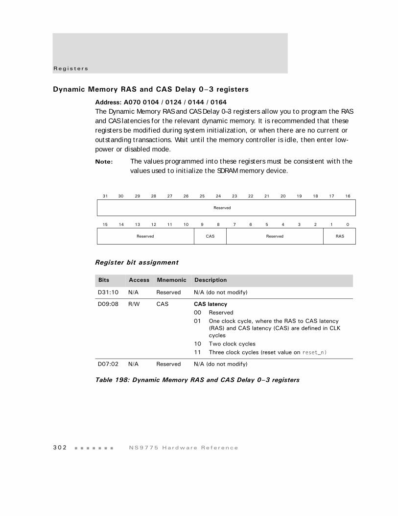
Reg i s t e r s
3 0 2 NS9775 Ha r dwa r e Re f e r ence
Dynamic Memory RAS and CAS Delay 0–3 registers
Address: A070 0104 / 0124 / 0144 / 0164The Dynamic Memory RAS and CAS Delay 0–3 registers allow you to program the RAS and CAS latencies for the relevant dynamic memory. It is recommended that these registers be modified during system initialization, or when there are no current or outstanding transactions. Wait until the memory controller is idle, then enter low-power or disabled mode.
Note: The values programmed into these registers must be consistent with the values used to initialize the SDRAM memory device.
Register bit assignment
Bits Access Mnemonic Description
D31:10 N/A Reserved N/A (do not modify)
D09:08 R/W CAS CAS latency00 Reserved01 One clock cycle, where the RAS to CAS latency
(RAS) and CAS latency (CAS) are defined in CLK cycles
10 Two clock cycles11 Three clock cycles (reset value on reset_n)
D07:02 N/A Reserved N/A (do not modify)
Table 198: Dynamic Memory RAS and CAS Delay 0–3 registers
13 12 11 10 9 8 7 6 5 4 3 2 1 015 14
31 29 28 27 26 25 24 23 22 21 20 19 18 17 1630
Reserved
Reserved CAS Reserved RAS
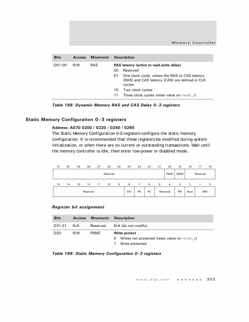
www.d i g i . com 303
Memo ry Con t r o l l e r
Static Memory Configuration 0–3 registers
Address: A070 0200 / 0220 / 0240 / 0260The Static Memory Configuration 0–3 registers configure the static memory configuration. It is recommended that these registers be modified during system initialization, or when there are no current or outstanding transactions. Wait until the memory controller is idle, then enter low-power or disabled mode.
Register bit assignment
D01:00 R/W RAS RAS latency (active to read.write delay)00 Reserved01 One clock cycle, where the RAS to CAS latency
(RAS) and CAS latency (CAS) are defined in CLK cycles
10 Two clock cycles11 Three clock cycles (reset value on reset_n)
Bits Access Mnemonic Description
Table 198: Dynamic Memory RAS and CAS Delay 0–3 registers
Bits Access Mnemonic Description
D31:21 N/A Reserved N/A (do not modify)
D20 R/W PSMC Write protect0 Writes not protected (reset value on reset_n)1 Write protected
Table 199: Static Memory Configuration 0–3 registers
13 12 11 10 9 8 7 6 5 4 3 2 1 015 14
31 29 28 27 26 25 24 23 22 21 20 19 18 17 1630
Reserved PSMC BSMC Reserved
Reserved EW PB PC Reserved PM Rsvd MW
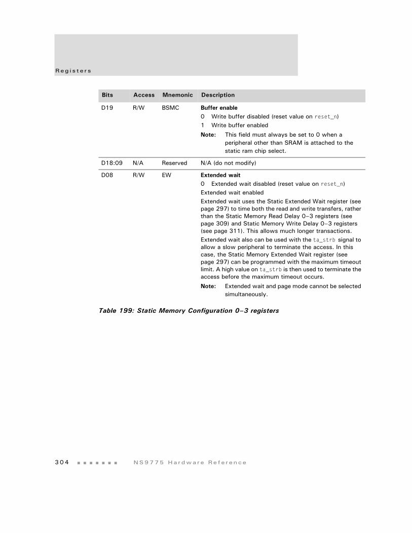
Reg i s t e r s
3 0 4 NS9775 Ha r dwa r e Re f e r ence
D19 R/W BSMC Buffer enable0 Write buffer disabled (reset value on reset_n)1 Write buffer enabled
Note: This field must always be set to 0 when a peripheral other than SRAM is attached to the static ram chip select.
D18:09 N/A Reserved N/A (do not modify)
D08 R/W EW Extended wait0 Extended wait disabled (reset value on reset_n)Extended wait enabledExtended wait uses the Static Extended Wait register (see page 297) to time both the read and write transfers, rather than the Static Memory Read Delay 0–3 registers (see page 309) and Static Memory Write Delay 0–3 registers (see page 311). This allows much longer transactions.Extended wait also can be used with the ta_strb signal to allow a slow peripheral to terminate the access. In this case, the Static Memory Extended Wait register (see page 297) can be programmed with the maximum timeout limit. A high value on ta_strb is then used to terminate the access before the maximum timeout occurs.
Note: Extended wait and page mode cannot be selected simultaneously.
Bits Access Mnemonic Description
Table 199: Static Memory Configuration 0–3 registers
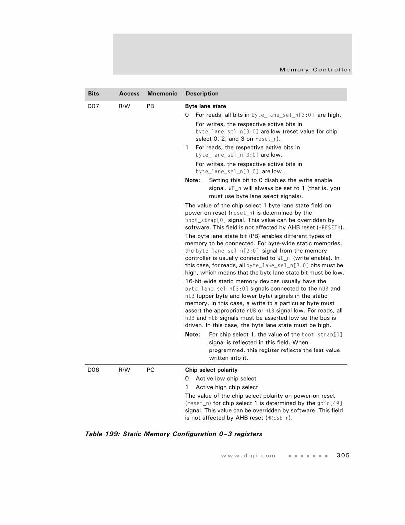
www.d i g i . com 305
Memo ry Con t r o l l e r
D07 R/W PB Byte lane state0 For reads, all bits in byte_lane_sel_n[3:0] are high.
For writes, the respective active bits in byte_lane_sel_n[3:0] are low (reset value for chip select 0, 2, and 3 on reset_n).
1 For reads, the respective active bits in byte_lane_sel_n[3:0] are low.
For writes, the respective active bits in byte_lane_sel_n[3:0] are low.
Note: Setting this bit to 0 disables the write enable signal. WE_n will always be set to 1 (that is, you must use byte lane select signals).
The value of the chip select 1 byte lane state field on power-on reset (reset_n) is determined by the boot_strap[0] signal. This value can be overridden by software. This field is not affected by AHB reset (HRESETn).The byte lane state bit (PB) enables different types of memory to be connected. For byte-wide static memories, the byte_lane_sel_n[3:0] signal from the memory controller is usually connected to WE_n (write enable). In this case, for reads, all byte_lane_sel_n[3:0] bits must be high, which means that the byte lane state bit must be low.16-bit wide static memory devices usually have the byte_lane_sel_n[3:0] signals connected to the nUB and nLB (upper byte and lower byte) signals in the static memory. In this case, a write to a particular byte must assert the appropriate nUB or nLB signal low. For reads, all nUB and nLB signals must be asserted low so the bus is driven. In this case, the byte lane state must be high.
Note: For chip select 1, the value of the boot-strap[0] signal is reflected in this field. When programmed, this register reflects the last value written into it.
D06 R/W PC Chip select polarity0 Active low chip select1 Active high chip selectThe value of the chip select polarity on power-on reset (reset_n) for chip select 1 is determined by the gpio[49] signal. This value can be overridden by software. This field is not affected by AHB reset (HRESETn).
Bits Access Mnemonic Description
Table 199: Static Memory Configuration 0–3 registers
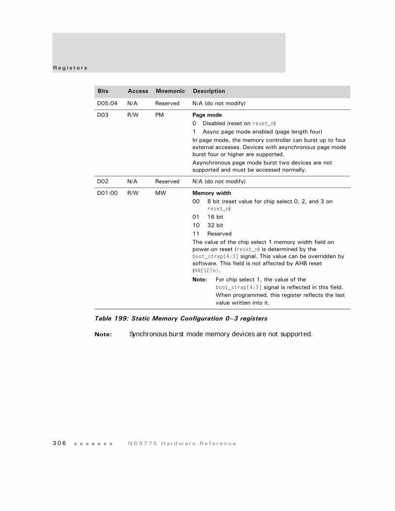
Reg i s t e r s
3 0 6 NS9775 Ha r dwa r e Re f e r ence
Note: Synchronous burst mode memory devices are not supported.
D05:04 N/A Reserved N/A (do not modify)
D03 R/W PM Page mode0 Disabled (reset on reset_n)1 Async page mode enabled (page length four)In page mode, the memory controller can burst up to four external accesses. Devices with asynchronous page mode burst four or higher are supported. Asynchronous page mode burst two devices are not supported and must be accessed normally.
D02 N/A Reserved N/A (do not modify)
D01:00 R/W MW Memory width00 8 bit (reset value for chip select 0, 2, and 3 on
reset_n)01 16 bit10 32 bit11 ReservedThe value of the chip select 1 memory width field on power-on reset (reset_n) is determined by the boot_strap[4:3] signal. This value can be overridden by software. This field is not affected by AHB reset (HRESETn).
Note: For chip select 1, the value of the boot_strap[4:3] signal is reflected in this field. When programmed, this register reflects the last value written into it.
Bits Access Mnemonic Description
Table 199: Static Memory Configuration 0–3 registers
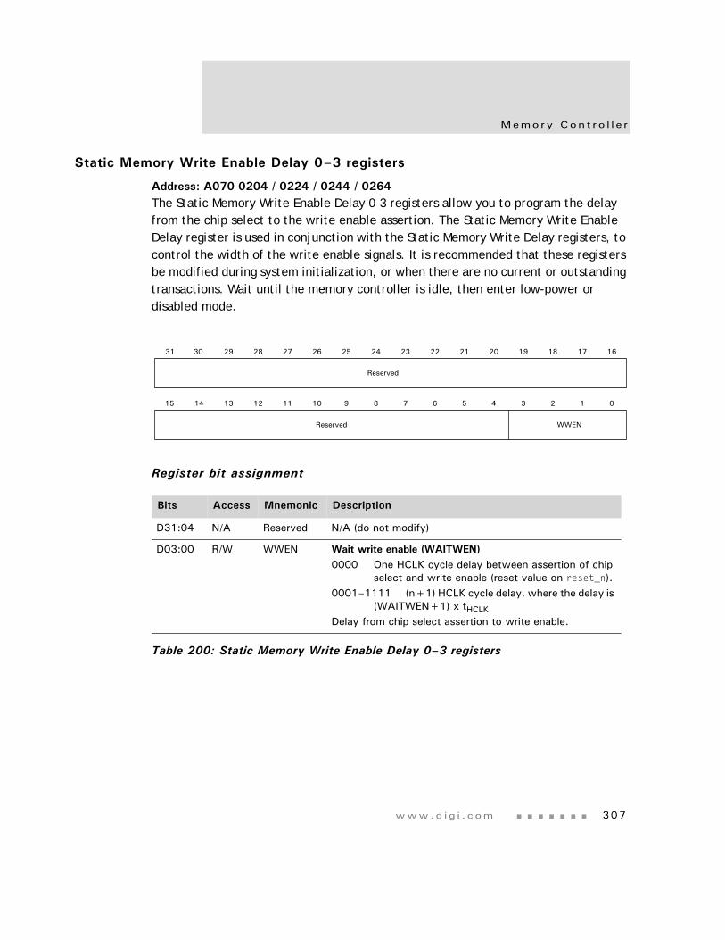
www.d i g i . com 307
Memo ry Con t r o l l e r
Static Memory Write Enable Delay 0–3 registers
Address: A070 0204 / 0224 / 0244 / 0264The Static Memory Write Enable Delay 0–3 registers allow you to program the delay from the chip select to the write enable assertion. The Static Memory Write Enable Delay register is used in conjunction with the Static Memory Write Delay registers, to control the width of the write enable signals. It is recommended that these registers be modified during system initialization, or when there are no current or outstanding transactions. Wait until the memory controller is idle, then enter low-power or disabled mode.
Register bit assignment
Bits Access Mnemonic Description
D31:04 N/A Reserved N/A (do not modify)
D03:00 R/W WWEN Wait write enable (WAITWEN)0000 One HCLK cycle delay between assertion of chip
select and write enable (reset value on reset_n).0001–1111 (n+1) HCLK cycle delay, where the delay is
(WAITWEN+1) x tHCLKDelay from chip select assertion to write enable.
Table 200: Static Memory Write Enable Delay 0–3 registers
13 12 11 10 9 8 7 6 5 4 3 2 1 015 14
31 29 28 27 26 25 24 23 22 21 20 19 18 17 1630
Reserved
Reserved WWEN
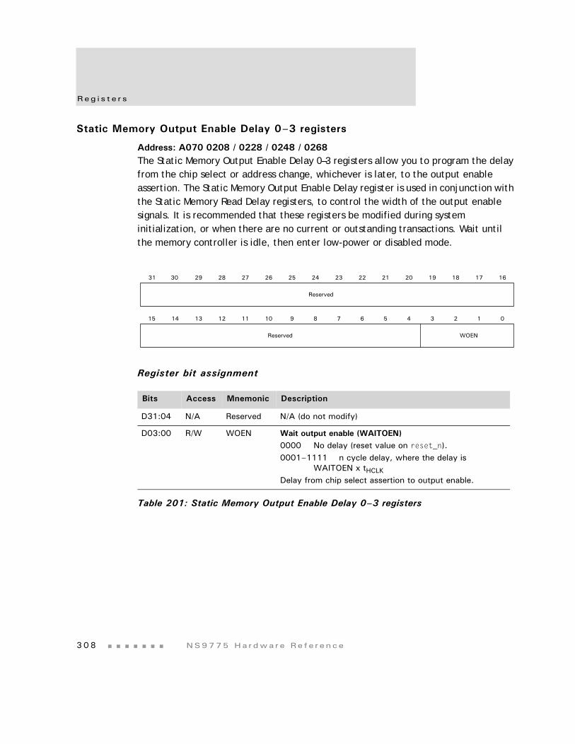
Reg i s t e r s
3 0 8 NS9775 Ha r dwa r e Re f e r ence
Static Memory Output Enable Delay 0–3 registers
Address: A070 0208 / 0228 / 0248 / 0268The Static Memory Output Enable Delay 0–3 registers allow you to program the delay from the chip select or address change, whichever is later, to the output enable assertion. The Static Memory Output Enable Delay register is used in conjunction with the Static Memory Read Delay registers, to control the width of the output enable signals. It is recommended that these registers be modified during system initialization, or when there are no current or outstanding transactions. Wait until the memory controller is idle, then enter low-power or disabled mode.
Register bit assignment
Bits Access Mnemonic Description
D31:04 N/A Reserved N/A (do not modify)
D03:00 R/W WOEN Wait output enable (WAITOEN)0000 No delay (reset value on reset_n).0001–1111 n cycle delay, where the delay is
WAITOEN x tHCLKDelay from chip select assertion to output enable.
Table 201: Static Memory Output Enable Delay 0–3 registers
13 12 11 10 9 8 7 6 5 4 3 2 1 015 14
31 29 28 27 26 25 24 23 22 21 20 19 18 17 1630
Reserved
Reserved WOEN
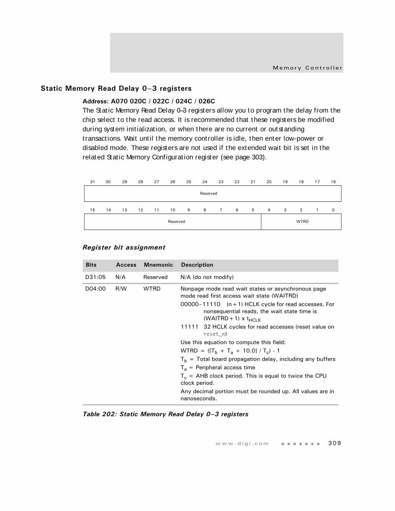
www.d i g i . com 309
Memo ry Con t r o l l e r
Static Memory Read Delay 0–3 registers
Address: A070 020C / 022C / 024C / 026CThe Static Memory Read Delay 0–3 registers allow you to program the delay from the chip select to the read access. It is recommended that these registers be modified during system initialization, or when there are no current or outstanding transactions. Wait until the memory controller is idle, then enter low-power or disabled mode. These registers are not used if the extended wait bit is set in the related Static Memory Configuration register (see page 303).
Register bit assignment
Bits Access Mnemonic Description
D31:05 N/A Reserved N/A (do not modify)
D04:00 R/W WTRD Nonpage mode read wait states or asynchronous page mode read first access wait state (WAITRD)00000–11110 (n+1) HCLK cycle for read accesses. For
nonsequential reads, the wait state time is (WAITRD+1) x tHCLK
11111 32 HCLK cycles for read accesses (reset value on reset_n)
Use this equation to compute this field:WTRD = ([Tb + Ta + 10.0] / Tc) - 1Tb = Total board propagation delay, including any buffersTa = Peripheral access timeTc = AHB clock period. This is equal to twice the CPU clock period.Any decimal portion must be rounded up. All values are in nanoseconds.
Table 202: Static Memory Read Delay 0–3 registers
13 12 11 10 9 8 7 6 5 4 3 2 1 015 14
31 29 28 27 26 25 24 23 22 21 20 19 18 17 1630
Reserved
Reserved WTRD
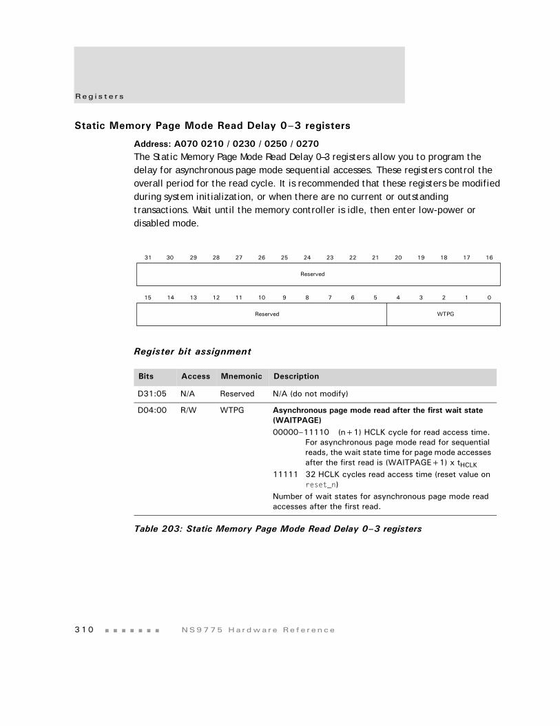
Reg i s t e r s
3 1 0 NS9775 Ha r dwa r e Re f e r ence
Static Memory Page Mode Read Delay 0–3 registers
Address: A070 0210 / 0230 / 0250 / 0270The Static Memory Page Mode Read Delay 0–3 registers allow you to program the delay for asynchronous page mode sequential accesses. These registers control the overall period for the read cycle. It is recommended that these registers be modified during system initialization, or when there are no current or outstanding transactions. Wait until the memory controller is idle, then enter low-power or disabled mode.
Register bit assignment
Bits Access Mnemonic Description
D31:05 N/A Reserved N/A (do not modify)
D04:00 R/W WTPG Asynchronous page mode read after the first wait state (WAITPAGE)00000–11110 (n+1) HCLK cycle for read access time.
For asynchronous page mode read for sequential reads, the wait state time for page mode accesses after the first read is (WAITPAGE+1) x tHCLK
11111 32 HCLK cycles read access time (reset value on reset_n)
Number of wait states for asynchronous page mode read accesses after the first read.
Table 203: Static Memory Page Mode Read Delay 0–3 registers
13 12 11 10 9 8 7 6 5 4 3 2 1 015 14
31 29 28 27 26 25 24 23 22 21 20 19 18 17 1630
Reserved
Reserved WTPG
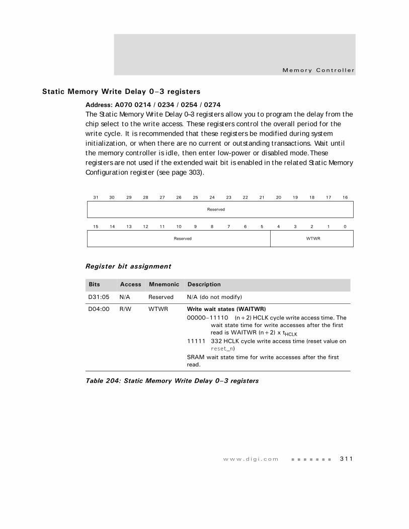
www.d i g i . com 311
Memo ry Con t r o l l e r
Static Memory Write Delay 0–3 registers
Address: A070 0214 / 0234 / 0254 / 0274The Static Memory Write Delay 0–3 registers allow you to program the delay from the chip select to the write access. These registers control the overall period for the write cycle. It is recommended that these registers be modified during system initialization, or when there are no current or outstanding transactions. Wait until the memory controller is idle, then enter low-power or disabled mode.These registers are not used if the extended wait bit is enabled in the related Static Memory Configuration register (see page 303).
Register bit assignment
Bits Access Mnemonic Description
D31:05 N/A Reserved N/A (do not modify)
D04:00 R/W WTWR Write wait states (WAITWR)00000–11110 (n+2) HCLK cycle write access time. The
wait state time for write accesses after the first read is WAITWR (n+2) x tHCLK
11111 332 HCLK cycle write access time (reset value on reset_n)
SRAM wait state time for write accesses after the first read.
Table 204: Static Memory Write Delay 0–3 registers
13 12 11 10 9 8 7 6 5 4 3 2 1 015 14
31 29 28 27 26 25 24 23 22 21 20 19 18 17 1630
Reserved
Reserved WTWR
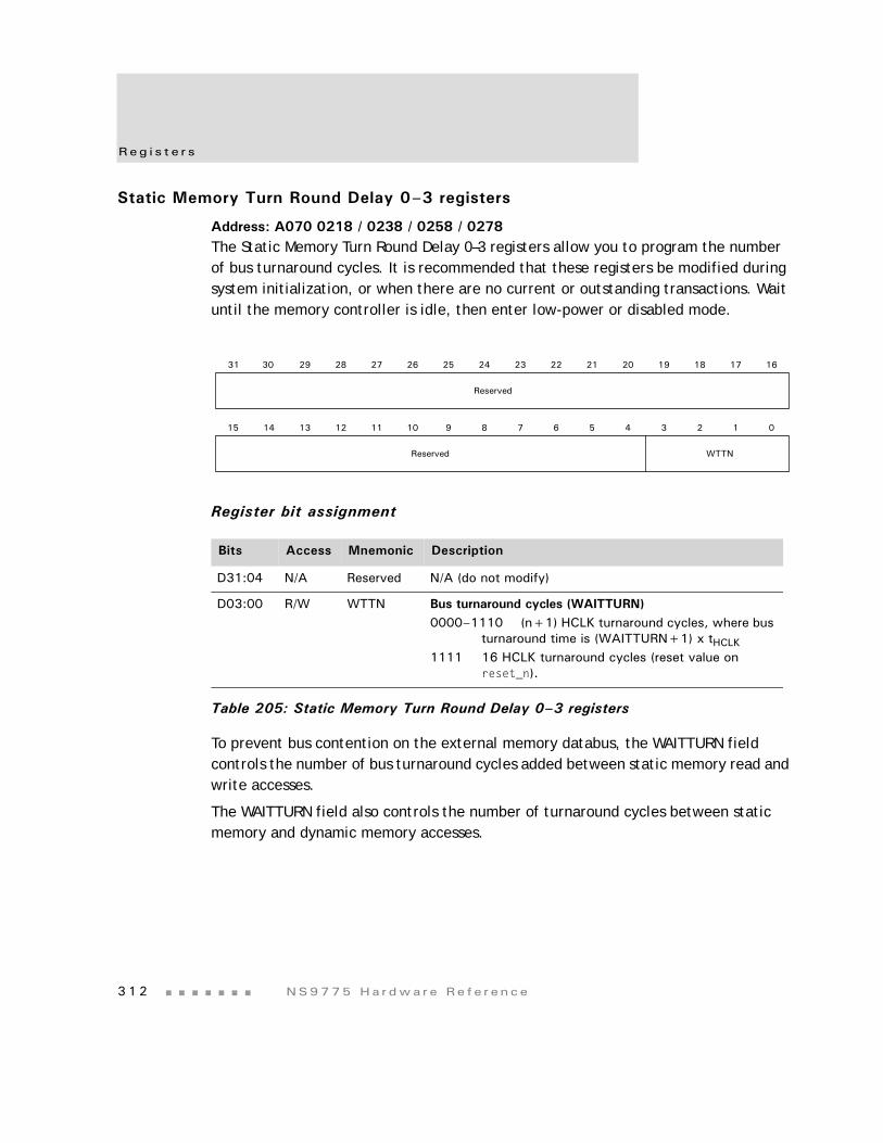
Reg i s t e r s
3 1 2 NS9775 Ha r dwa r e Re f e r ence
Static Memory Turn Round Delay 0–3 registers
Address: A070 0218 / 0238 / 0258 / 0278The Static Memory Turn Round Delay 0–3 registers allow you to program the number of bus turnaround cycles. It is recommended that these registers be modified during system initialization, or when there are no current or outstanding transactions. Wait until the memory controller is idle, then enter low-power or disabled mode.
Register bit assignment
To prevent bus contention on the external memory databus, the WAITTURN field controls the number of bus turnaround cycles added between static memory read and write accesses.
The WAITTURN field also controls the number of turnaround cycles between static memory and dynamic memory accesses.
Bits Access Mnemonic Description
D31:04 N/A Reserved N/A (do not modify)
D03:00 R/W WTTN Bus turnaround cycles (WAITTURN)0000–1110 (n+1) HCLK turnaround cycles, where bus
turnaround time is (WAITTURN+1) x tHCLK1111 16 HCLK turnaround cycles (reset value on
reset_n).
Table 205: Static Memory Turn Round Delay 0–3 registers
13 12 11 10 9 8 7 6 5 4 3 2 1 015 14
31 29 28 27 26 25 24 23 22 21 20 19 18 17 1630
Reserved
Reserved WTTN

www.d i g i . com 313
Memo ry Con t r o l l e r

Reg i s t e r s
3 1 4 NS9775 Ha r dwa r e Re f e r ence

www.d i g i . com 315
Memo ry Con t r o l l e r

Reg i s t e r s
3 1 6 NS9775 Ha r dwa r e Re f e r ence

www.d i g i . com 317
Memo ry Con t r o l l e r

Reg i s t e r s
3 1 8 NS9775 Ha r dwa r e Re f e r ence

www.d i g i . com 319
Memo ry Con t r o l l e r

Reg i s t e r s
3 2 0 NS9775 Ha r dwa r e Re f e r ence

www.d i g i . com 321
Memo ry Con t r o l l e r

Reg i s t e r s
3 2 2 NS9775 Ha r dwa r e Re f e r ence

www.d i g i . com 323
Memo ry Con t r o l l e r

325
Ethernet Communication ModuleC H A P T E R 6
The Ethernet Communication module consists of an Ethernet Media Access Controller (MAC) and Ethernet front-end module. The Ethernet MAC interfaces to an external PHY through one of two industry-standard interfaces: MII and RMII. The Ethernet front-end module provides all of the control functions to the MAC.
Ove r v i ew
3 2 6 NS9775 Ha r dwa r e Re f e r ence
Overview
The Ethernet MAC module provides the following:
Station address logic (SAL)
Statistics module
Interface to MII (Media Independent Interface) PHY
Interface to RMII (Reduced Media Independent Interface) PHY
The Ethernet front-end module does the following:
Provides control functions to the MAC
Buffers and filters the frames received from the MAC
Pumps transmit data into the MAC
Moves frames between the MAC and the system memory
Reports transmit and receive status to the host
“Legend”RX_RD = Receive read
RX_WR = Receive write
TX_RD = Transmit read
TX_WR = Transmit write
Figure 64 shows the Ethernet Communications module.
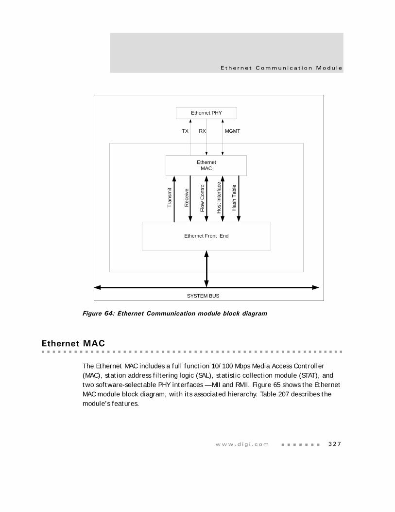
www.d i g i . com 327
E t he r n e t Commun i c a t i o n Modu l e
Figure 64: Ethernet Communication module block diagram
Ethernet MAC
The Ethernet MAC includes a full function 10/100 Mbps Media Access Controller (MAC), station address filtering logic (SAL), statistic collection module (STAT), and two software-selectable PHY interfaces — MII and RMII. Figure 65 shows the Ethernet MAC module block diagram, with its associated hierarchy. Table 207 describes the module’s features.
EthernetMAC
Ethernet Front End
Ethernet PHY
TX RX
Tran
smit
Rec
eive
Flow
Con
trol
Hos
t Int
erfa
ce
Has
h Ta
ble
SYSTEM BUS
MGMT
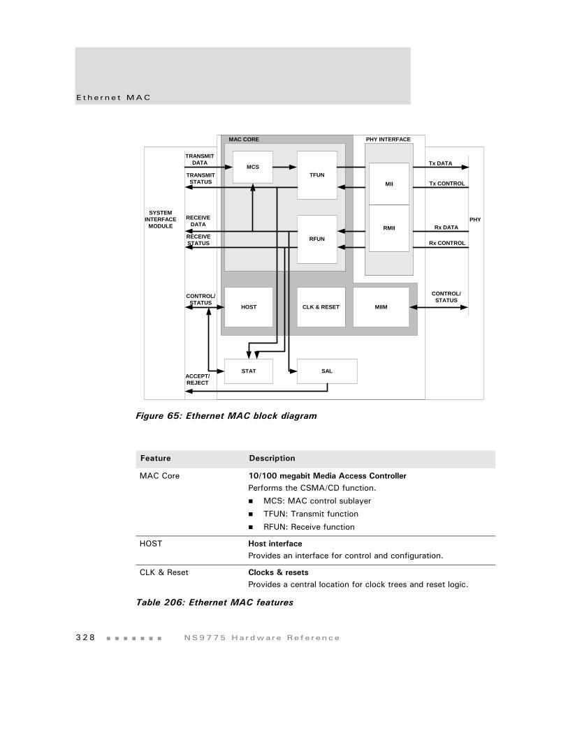
E t he r n e t MAC
3 2 8 NS9775 Ha r dwa r e Re f e r ence
Figure 65: Ethernet MAC block diagram
Feature Description
MAC Core 10/100 megabit Media Access ControllerPerforms the CSMA/CD function.
MCS: MAC control sublayer
TFUN: Transmit function
RFUN: Receive function
HOST Host interfaceProvides an interface for control and configuration.
CLK & Reset Clocks & resetsProvides a central location for clock trees and reset logic.
Table 206: Ethernet MAC features
TFUN
RFUN
MCS
CLK & RESET MIIMHOST
MAC CORE PHY INTERFACE
PHYSYSTEM
INTERFACEMODULE
Tx DATA
Tx CONTROL
Rx DATA
Rx CONTROL
CONTROL/STATUS
CONTROL/STATUS
TRANSMITDATA
TRANSMITSTATUS
RECEIVEDATA
RECEIVESTATUS
STAT SALACCEPT/REJECT
MII
RMII
www.d i g i . com 329
E t he r n e t Commun i c a t i o n Modu l e
MIIM MII managementProvides control/status path to MII and RMII PHYs.
STAT Statistics moduleCounts and saves Ethernet statistics.
SAL Station address logicPerforms destination address filtering.
MII Media Independent InterfaceProvides the interface from the MAC core to a PHY that supports the MII (as described in the IEEE 802.3 standard).
RMII Reduced Media Independent InterfaceProvides the interface from the MAC core to a PHY that supports RMII.Advisory: Note that the NS9775 RMII interface incorrectly
handles packets with dribble. (Dribble occurs when extra data is detected on the end of a packet, but there is insufficient data to form a new byte.)
In some cases, packets with dribble will be passed through with the extra data truncated; this is the correct handling, and the packet is treated as a normal packet without error.
In other cases, packets with dribble will be passed through with an extra byte at the end. In these situations, the packet is rejected correctly because it appears to have an invalid FCS.
In addition, the dribble bit (RXDR) in the status field of RX Ethernet packets and in the Ethernet Receive Status register (see "Ethernet Receive Status register" on page 358) may be falsely set for packets that do not have any dribble bits. For RMII, the dribble bit should be ignored.
For RMII, ignore the Receive Alignment Error Counter and the Receive FCS Error Counter. Set the M1RFC and M1RAL bits in the Carry Register 1 Mask register to 1 so no interrupts will be caused when these counters overflow.
Feature Description
Table 206: Ethernet MAC features
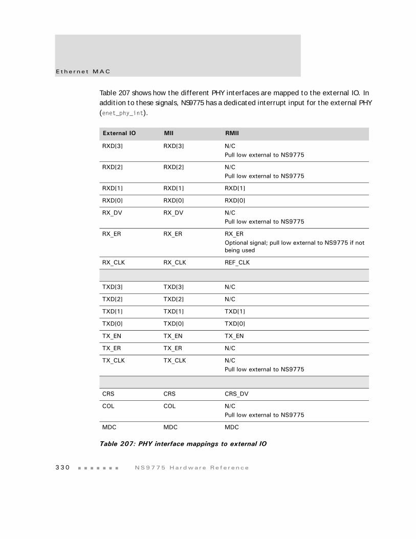
E t he r n e t MAC
3 3 0 NS9775 Ha r dwa r e Re f e r ence
Table 207 shows how the different PHY interfaces are mapped to the external IO. In addition to these signals, NS9775 has a dedicated interrupt input for the external PHY (enet_phy_int).
External IO MII RMII
RXD[3] RXD[3] N/CPull low external to NS9775
RXD[2] RXD[2] N/CPull low external to NS9775
RXD[1] RXD[1] RXD[1]
RXD[0] RXD[0] RXD[0]
RX_DV RX_DV N/CPull low external to NS9775
RX_ER RX_ER RX_EROptional signal; pull low external to NS9775 if not being used
RX_CLK RX_CLK REF_CLK
TXD[3] TXD[3] N/C
TXD[2] TXD[2] N/C
TXD[1] TXD[1] TXD[1]
TXD[0] TXD[0] TXD[0]
TX_EN TX_EN TX_EN
TX_ER TX_ER N/C
TX_CLK TX_CLK N/CPull low external to NS9775
CRS CRS CRS_DV
COL COL N/CPull low external to NS9775
MDC MDC MDC
Table 207: PHY interface mappings to external IO
www.d i g i . com 331
E t he r n e t Commun i c a t i o n Modu l e
Station address logic (SAL)
The station address logic module examines the destination address field of incoming frames, and filters the frames before they are stored in the Ethernet front-end module. The filtering options, listed next, are programmed in the Station Address Filter register (see page 377).
Accept frames to destination address programmed in the SA1, SA2, and SA3 registers (Station Address registers, beginning on page 375)
Accept all frames
Accept all multicast frames
Accept all multicast frames using HT1 and HT2 registers (Hash Table registers, beginning on page 377)
Accept all broadcast frames
The filtering conditions are independent of each other; for example, the Station Address Logic register can be configured to accept all broadcast frames, and frames to the programmed destination address.
The MAC receiver provides the station address logic with a 6-bit CRC value that is the upper 6 bits of a 32-bit CRC calculation performed on the 48-bit multicast destination address. This 6-bit value addresses the 64-bit multicast hash table created in the HT1 and HT2 registers (see "Register Hash Tables" on page 377). If the current receive frame is a multicast frame and the 6-bit CRC addresses a bit in the hash table that is set to 1, the receive frame is accepted; otherwise, the frame is rejected. See "Sample hash table code," beginning on page 409, for sample C code to calculate hash table entries.
Statistics module
The Statistics module counts and saves Ethernet statistics in several counters (see "Statistics registers" on page 379).
MDIO MDIO MDIO
External IO MII RMII
Table 207: PHY interface mappings to external IO
E t he r n e t MAC
3 3 2 NS9775 Ha r dwa r e Re f e r ence
The Ethernet General Control Register #2 contains three statistics module configuration bits:
AUTOZ. Enable statistics counter clear on read.
CLRCNT. Clear statistics counters.
STEN. Enable statistics counters.
If any of the counters roll over, an associated carry bit is set in the Carry 1 (CAR1) or Carry 2 (CAR2) registers (see "General Statistics registers," beginning on page 388). Any statistics counter overflow can cause the STOVFL bit in the Ethernet Interrupt Status register (see page 396) to be set if its associated mask bit is not set in Carry Mask Register 1 or Carry Mask Register 2 (see "General Statistics registers," beginning on page 388).
The counters support a clear on read capability that is enabled when AUTOZ is set to 1 in the Ethernet General Control Register #2.
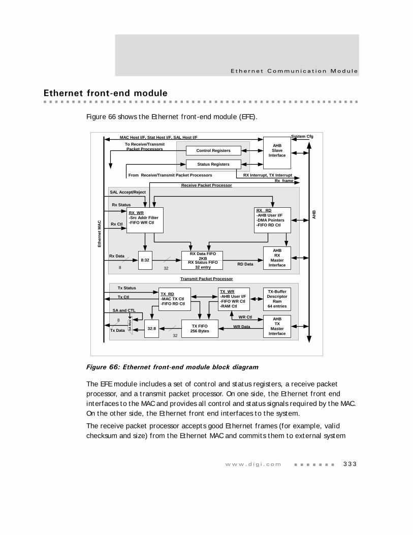
www.d i g i . com 333
E t he r n e t Commun i c a t i o n Modu l e
Ethernet front-end module
Figure 66 shows the Ethernet front-end module (EFE).
Figure 66: Ethernet front-end module block diagram
The EFE module includes a set of control and status registers, a receive packet processor, and a transmit packet processor. On one side, the Ethernet front end interfaces to the MAC and provides all control and status signals required by the MAC. On the other side, the Ethernet front end interfaces to the system.
The receive packet processor accepts good Ethernet frames (for example, valid checksum and size) from the Ethernet MAC and commits them to external system
TX FIFO256 Bytes
AHBTX
MasterInterface
Control Registers
Ethe
rnet
MA
C
Tx Data
RD Data
WR Data
AH
B
AHBSlave
Interface
TX_WR-AHB User I/F-FIFO WR Ctl-RAM Ctl
TX_RD-MAC TX Ctl-FIFO RD Ctl
TX-BufferDescriptor
Ram64 entries
32:8
8
32
Tx Ctl
Tx Status
WR Ctl
RX _RD-AHB User I/F-DMA Pointers-FIFO RD Ctl
8:32
RX_WR-Src Addr Filter-FIFO WR Ctl
AHBRX
MasterInterface
Rx Data
Rx Status
Rx Ctl
SAL Accept/Reject
Status Registers
MAC Host I/F, Stat Host I/F, SAL Host I/F
RX Interrupt, TX Interrupt
To Receive/TransmitPacket Processors
8 32
Receive Packet Processor
Transmit Packet Processor
System Cfg
Rx_frame
SA and CTL
SA M
ux
From Receive/Transmit Packet Processors
RX Data FIFO2KB
RX Status FIFO32 entry
E t he r n e t f r on t - end modu l e
3 3 4 NS9775 Ha r dwa r e Re f e r ence
memory. Bad frames (for example, invalid checksum or code violation) and frames with unacceptable destination addresses are discarded.
The 2K byte RX_FIFO allows the entire Ethernet frame to be buffered while the receive byte count is analyzed. The receive byte count is analyzed by the receive packet processor to select the optimum-sized buffer for transferring the received frame to system memory. The processor can use one of four different-sized receive buffers in system memory.
The transmit packet processor transfers frames constructed in system memory to the Ethernet MAC. The software initializes a buffer descriptor table in a local RAM that points the transmit packet processor to the various frame segments in system memory. The 256-byte TX_FIFO decouples the data transfer to the Ethernet MAC from the AHB bus fill rate.
Receive packet processor
As a frame is received from the Ethernet MAC, it is stored in the receive data FIFO. At the end of the frame, an accept/reject decision is made based on several conditions. If the packet is rejected, it is essentially flushed from the receive data FIFO.
If a frame is accepted, status signals from the MAC, including the receive size of the frame, are stored in a separate 32-entry receive status FIFO; the RX_RD logic is notified that a good frame is in the FIFO.
If the RX_WR logic tries to write a full receive data FIFO anytime during the frame, it flushes the frame from the receive data FIFO and sets RXOVFL_DATA (RX data FIFO overflowed) in the Ethernet Interrupt Status register. For proper operation, reset the receive packet processor using the ERX bit in the Ethernet General Control Register #1 when this condition occurs. If the RX_WR logic tries to write a full receive status FIFO at the end of the frame, the RX_WR logic flushes the frame from the receive data FIFO and sets RXOVFL_STAT (RX status FIFO overflowed) in the Ethernet Interrupt Status register.
Power down mode
The RX_WR logic supports the NS9775’s system power down and recovery functionality. In this mode, the RX clock to the MAC and the RX_WR logic are still active, but the clock to the RX_RD and AHB interface is disabled. This allows frames to be received
www.d i g i . com 335
E t he r n e t Commun i c a t i o n Modu l e
and written into the receive FIFO, but the frame remains in the FIFO until the system wakes up. Normal frame filtering is still performed.
When a qualified frame is inserted into the receive FIFO, the receive packet processor notifies the system power controller, which performs the wake up sequence. The frame remains in the receive FIFO until the system wakes up.
Transferring a frame to system memory
The RX_RD logic manages the transfer of a frame in the RX_FIFO to system memory. The transfer is enabled by setting the ERXDMA (enable receive DMA) bit in Ethernet General Control Register #1.
Transferring a frame in the receive FIFO to system memory begins when the RX_WR logic notifies the RX_RD logic that a good frame is in the receive FIFO. Frames are transferred to system memory using up to four rings (that is, 1, 2, or 3 rings can also be used) of buffer descriptors that point to buffers in system memory. The maximum frame size that each ring can accept is programmable. The first thing the RX_RD logic does, then, is analyze the frame length in the receive status FIFO to determine which buffer descriptor to use.
The RX_RD logic goes through the four buffer descriptors looking for the optimum buffer size. It searches the enabled descriptors starting with A, then B, C, and finally D; any pools that are full (that is, the F bit is set in the buffer descriptor) are skipped. The search stops as soon as the logic encounters an available buffer that is large enough to hold the entire receive frame.
The pointers to the first buffer descriptor in each of the four pools are found in the related Buffer Descriptor Pointer register (RXAPTR, RXBPTR, RXCPTR, RXDPTR). Pointers to subsequent buffer descriptors are generated by adding an offset of 0x10 from this pointer for each additional buffer used.
Figure 67 shows the format of the buffer descriptors. The current buffer descriptor for each pool is kept in local registers. The current buffer descriptor registers are initialized to the buffer descriptors pointed to by the Buffer Descriptor Pointer registers, by setting the ERXINIT (enable initialization of RX buffer descriptor registers) bit in Ethernet General Control Register #1. The initialization process is complete when RXINIT (RX initialization complete) is set in the Ethernet General Status register. At the end of a frame, the next buffer descriptor for the ring just
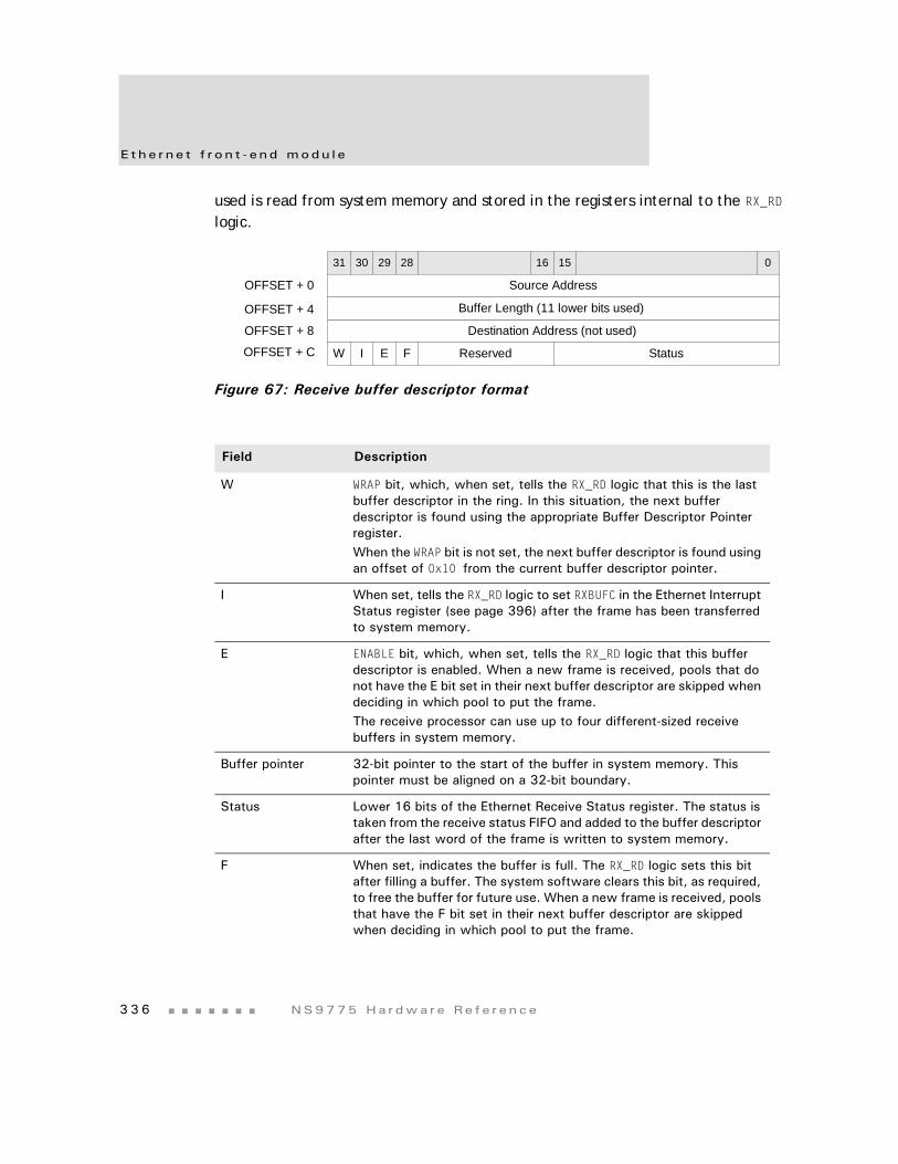
E t he r n e t f r on t - end modu l e
3 3 6 NS9775 Ha r dwa r e Re f e r ence
used is read from system memory and stored in the registers internal to the RX_RD logic.
Figure 67: Receive buffer descriptor format
Field Description
W WRAP bit, which, when set, tells the RX_RD logic that this is the last buffer descriptor in the ring. In this situation, the next buffer descriptor is found using the appropriate Buffer Descriptor Pointer register. When the WRAP bit is not set, the next buffer descriptor is found using an offset of 0x10 from the current buffer descriptor pointer.
I When set, tells the RX_RD logic to set RXBUFC in the Ethernet Interrupt Status register (see page 396) after the frame has been transferred to system memory.
E ENABLE bit, which, when set, tells the RX_RD logic that this buffer descriptor is enabled. When a new frame is received, pools that do not have the E bit set in their next buffer descriptor are skipped when deciding in which pool to put the frame.The receive processor can use up to four different-sized receive buffers in system memory.
Buffer pointer 32-bit pointer to the start of the buffer in system memory. This pointer must be aligned on a 32-bit boundary.
Status Lower 16 bits of the Ethernet Receive Status register. The status is taken from the receive status FIFO and added to the buffer descriptor after the last word of the frame is written to system memory.
F When set, indicates the buffer is full. The RX_RD logic sets this bit after filling a buffer. The system software clears this bit, as required, to free the buffer for future use. When a new frame is received, pools that have the F bit set in their next buffer descriptor are skipped when deciding in which pool to put the frame.
Destination Address (not used)
Buffer Length (11 lower bits used)
Status
Source Address
0
OFFSET + 0
OFFSET + 4
OFFSET + 8
OFFSET + C FI EW Reserved
31 151630 29 28
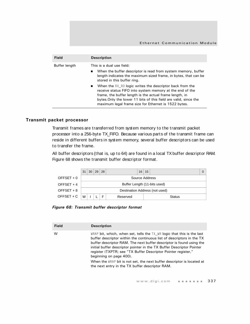
www.d i g i . com 337
E t he r n e t Commun i c a t i o n Modu l e
Transmit packet processor
Transmit frames are transferred from system memory to the transmit packet processor into a 256-byte TX_FIFO. Because various parts of the transmit frame can reside in different buffers in system memory, several buffer descriptors can be used to transfer the frame.
All buffer descriptors (that is, up to 64) are found in a local TX buffer descriptor RAM. Figure 68 shows the transmit buffer descriptor format.
Figure 68: Transmit buffer descriptor format
Buffer length This is a dual use field:
When the buffer descriptor is read from system memory, buffer length indicates the maximum sized frame, in bytes, that can be stored in this buffer ring.
When the RX_RD logic writes the descriptor back from the receive status FIFO into system memory at the end of the frame, the buffer length is the actual frame length, in bytes.Only the lower 11 bits of this field are valid, since the maximum legal frame size for Ethernet is 1522 bytes.
Field Description
Field Description
W WRAP bit, which, when set, tells the TX_WR logic that this is the last buffer descriptor within the continuous list of descriptors in the TX buffer descriptor RAM. The next buffer descriptor is found using the initial buffer descriptor pointer in the TX Buffer Descriptor Pointer register (TXPTR; see "TX Buffer Descriptor Pointer register," beginning on page 400).When the WRAP bit is not set, the next buffer descriptor is located at the next entry in the TX buffer descriptor RAM.
Destination Address (not used)
Buffer Length (11-bits used)
Status
Source Address
0
OFFSET + 0
OFFSET + 4
OFFSET + 8
OFFSET + C FI LW Reserved
31 151630 29 28
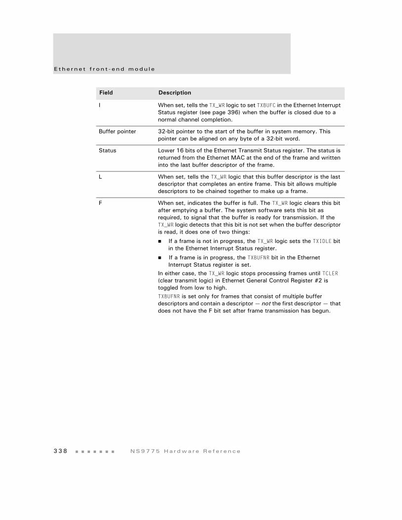
E t he r n e t f r on t - end modu l e
3 3 8 NS9775 Ha r dwa r e Re f e r ence
I When set, tells the TX_WR logic to set TXBUFC in the Ethernet Interrupt Status register (see page 396) when the buffer is closed due to a normal channel completion.
Buffer pointer 32-bit pointer to the start of the buffer in system memory. This pointer can be aligned on any byte of a 32-bit word.
Status Lower 16 bits of the Ethernet Transmit Status register. The status is returned from the Ethernet MAC at the end of the frame and written into the last buffer descriptor of the frame.
L When set, tells the TX_WR logic that this buffer descriptor is the last descriptor that completes an entire frame. This bit allows multiple descriptors to be chained together to make up a frame.
F When set, indicates the buffer is full. The TX_WR logic clears this bit after emptying a buffer. The system software sets this bit as required, to signal that the buffer is ready for transmission. If the TX_WR logic detects that this bit is not set when the buffer descriptor is read, it does one of two things:
If a frame is not in progress, the TX_WR logic sets the TXIDLE bit in the Ethernet Interrupt Status register.
If a frame is in progress, the TXBUFNR bit in the Ethernet Interrupt Status register is set.
In either case, the TX_WR logic stops processing frames until TCLER (clear transmit logic) in Ethernet General Control Register #2 is toggled from low to high.TXBUFNR is set only for frames that consist of multiple buffer descriptors and contain a descriptor — not the first descriptor — that does not have the F bit set after frame transmission has begun.
Field Description
www.d i g i . com 339
E t he r n e t Commun i c a t i o n Modu l e
Setting the EXTDMA (enable transmit DMA) bit in Ethernet General Control Register #1 starts the transfer of transmit frames from the system memory to the TX_FIFO. The TX_WR logic reads the first buffer descriptor in the TX buffer descriptor RAM.
If the F bit is set, it transfers data from system memory to the TX_FIFO using the buffer pointer as the starting point. This process continues until the end of the buffer is reached. The address for each subsequent read of the buffer is incremented by 32 bytes (that is, 0x20). The buffer length field in the buffer descriptor is decremented by this same value, each transfer, to identify when the end of the buffer is reached.
If the L field in the buffer descriptor is 0, the next buffer descriptor in the RAM continues the frame transfer until the L field in the current buffer descriptor is 1. This identifies the current buffer as the last buffer of a transmit frame.
After the entire frame has been written to the TX_FIFO, the TX_WR logic waits for a signal from the TX_RD logic indicating that frame transmission has completed at the MAC. The TX_WR logic updates the buffer length, status, and F fields of the current buffer descriptor (that is, the last buffer descriptor for the frame) in the TX buffer descriptor RAM when the signal is received.
The TX_WR logic examines the status received from the MAC after it has transmitted the frame.
Buffer length This is a dual use field:
When the buffer descriptor is read from the TX buffer descriptor RAM, buffer length indicates the length of the buffer, in bytes. The TX_WR logic uses this information to identify the end of the buffer. For proper operation of the TX_WR logic, all transmit frames must be at least 34 bytes in length.
When the TX_WR logic updates the buffer descriptor at the end of the frame, it writes the length of the frame, in bytes, into this field for the last buffer descriptor of the frame.
If the MAC is configured to add the CRC to the frame (that is, CRCEN in MAC Configuration Register #2 is set to 1), this field will include the four bytes of CRC. This field is set to 0x000 for jumbo frames that are aborted (see "TXAJ" on page 356)
Only the lower 11 bits of this field are valid, since the maximum legal frame size for Ethernet is 1522 bytes.
Field Description
E t he r n e t f r on t - end modu l e
3 4 0 NS9775 Ha r dwa r e Re f e r ence
If the frame was transmitted successfully, the TX_WR logic sets TXDONE (frame transmission complete) in the Ethernet Interrupt Status register and reads the next buffer descriptor. If a new frame is available (that is, the F bit is set), the TX_WR starts transferring the frame. If a new frame is not available, the TX_WR logic sets the TXIDLE (TX_WR logic has no frame to transmit) bit in the Ethernet Interrupt Status register and waits for the software to toggle TCLER (clear transmit logic), in Ethernet General Control Register #2, from low to high to resume processing. The TX_WR logic also loads the 8-bit TX buffer descriptor RAM address of the buffer descriptor that did not have the F bit set in the TX Stall Buffer Descriptor Pointer register (see page 402). This allows identification of the buffer descriptor that caused this condition. As part of the recovery procedure, software must read the TX Stall Buffer Descriptor Pointer register and then write the 8-bit address of the buffer descriptor to resume transmission into the TX Recover Buffer Descriptor Pointer register.
If the TX_WR logic detects that the frame was aborted or had an error, the logic updates the current buffer descriptor as described in the previous paragraph. If the frame was aborted before the last buffer descriptor of the frame was accessed, the result is a situation in which the status field of a buffer descriptor, which is not the last buffer descriptor in a frame, has a non-zero value. The TX_WR logic stops processing frames until TCLER (clear transmit logic) in Ethernet General Control Register #2 is toggled from low to high to resume processing. The TX_WR logic also sets TXERR (last frame not transmitted successfully) in the Ethernet Interrupt Status register and loads the TX buffer descriptor RAM address of the current buffer descriptor in the TX Error Buffer Descriptor Pointer register (see page 401). This allows identification of the frame that was not transmitted successfully. As part of the recovery procedure, software must read the TX Error Buffer Descriptor Pointer register and then write the 8-bit address of the buffer descriptor to resume transmission into the TX Recover Buffer Descriptor Pointer register.
Transmitting a frame to the Ethernet MAC
The TX_RD logic is responsible for reading data from the TX_FIFO and sending it to the Ethernet MAC. The logic does not begin reading a new frame until the TX_FIFO is full. This scheme decouples the data transfer to the Ethernet MAC from the fill rate from
www.d i g i . com 341
E t he r n e t Commun i c a t i o n Modu l e
the AHB bus. For short frames that are less than 256 bytes, the transmit process begins when the end-of-frame signal is received from the TX_WR logic.
When the MAC completes a frame transmission, it returns status bits that are stored in the Ethernet Transmit Status register (see page 354) and written into the status field of the current buffer descriptor.
Ethernet Slave Interface
The AHB slave interface supports only single 32-bit transfers. The slave interface also supports limiting CSR and RAM accesses to CPU “privileged mode” accesses. Use the internal register access mode bit 0 in the Miscellaneous System Configuration register to set access accordingly (see "Miscellaneous System Configuration and Status register," beginning on page 169).
The slave also generates an AHB ERROR if the address is not aligned on a 32-bit boundary, and the misaligned bus address response mode is set in the Miscellaneous System Configuration register (see "Miscellaneous System Configuration and Status register," beginning on page 169). In addition, accesses to non-existent addresses result in an AHB ERROR response.
Interrupts
Separate RX and TX interrupts are provided back to the system. Table 208 shows all interrupt sources and the interrupts to which they are assigned.
Interrupt condition Description Interrupt
RX data FIFO overflow RX data FIFO overflowed. For proper operation, reset the receive packet processor using the ERX bit in the Ethernet General Control Register #1 when this condition occurs.
RX
RX status FIFO overflow
RX status overflowed. RX
Receive buffer closed I bit set in receive buffer descriptor and buffer closed. RX
Receive complete (Pool A)
Complete receive frame stored in pool A of system memory.
RX
Table 208: Ethernet interrupt conditions
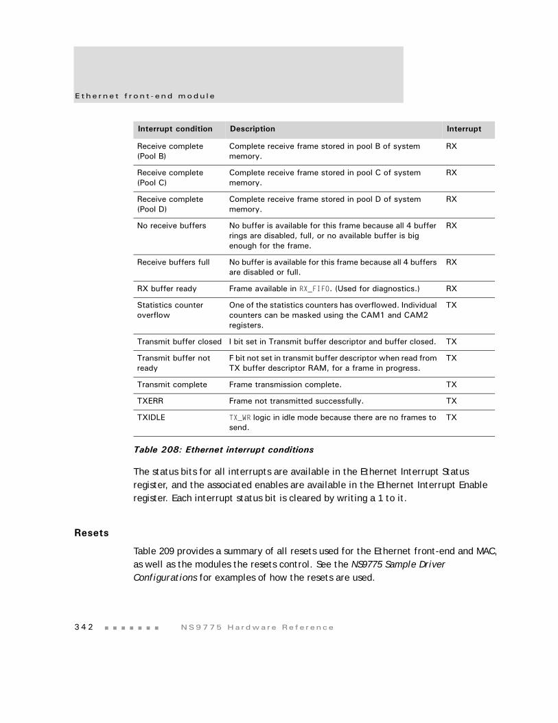
E t he r n e t f r on t - end modu l e
3 4 2 NS9775 Ha r dwa r e Re f e r ence
The status bits for all interrupts are available in the Ethernet Interrupt Status register, and the associated enables are available in the Ethernet Interrupt Enable register. Each interrupt status bit is cleared by writing a 1 to it.
Resets
Table 209 provides a summary of all resets used for the Ethernet front-end and MAC, as well as the modules the resets control. See the NS9775 Sample Driver Configurations for examples of how the resets are used.
Receive complete (Pool B)
Complete receive frame stored in pool B of system memory.
RX
Receive complete (Pool C)
Complete receive frame stored in pool C of system memory.
RX
Receive complete (Pool D)
Complete receive frame stored in pool D of system memory.
RX
No receive buffers No buffer is available for this frame because all 4 buffer rings are disabled, full, or no available buffer is big enough for the frame.
RX
Receive buffers full No buffer is available for this frame because all 4 buffers are disabled or full.
RX
RX buffer ready Frame available in RX_FIFO. (Used for diagnostics.) RX
Statistics counter overflow
One of the statistics counters has overflowed. Individual counters can be masked using the CAM1 and CAM2 registers.
TX
Transmit buffer closed I bit set in Transmit buffer descriptor and buffer closed. TX
Transmit buffer not ready
F bit not set in transmit buffer descriptor when read from TX buffer descriptor RAM, for a frame in progress.
TX
Transmit complete Frame transmission complete. TX
TXERR Frame not transmitted successfully. TX
TXIDLE TX_WR logic in idle mode because there are no frames to send.
TX
Interrupt condition Description Interrupt
Table 208: Ethernet interrupt conditions
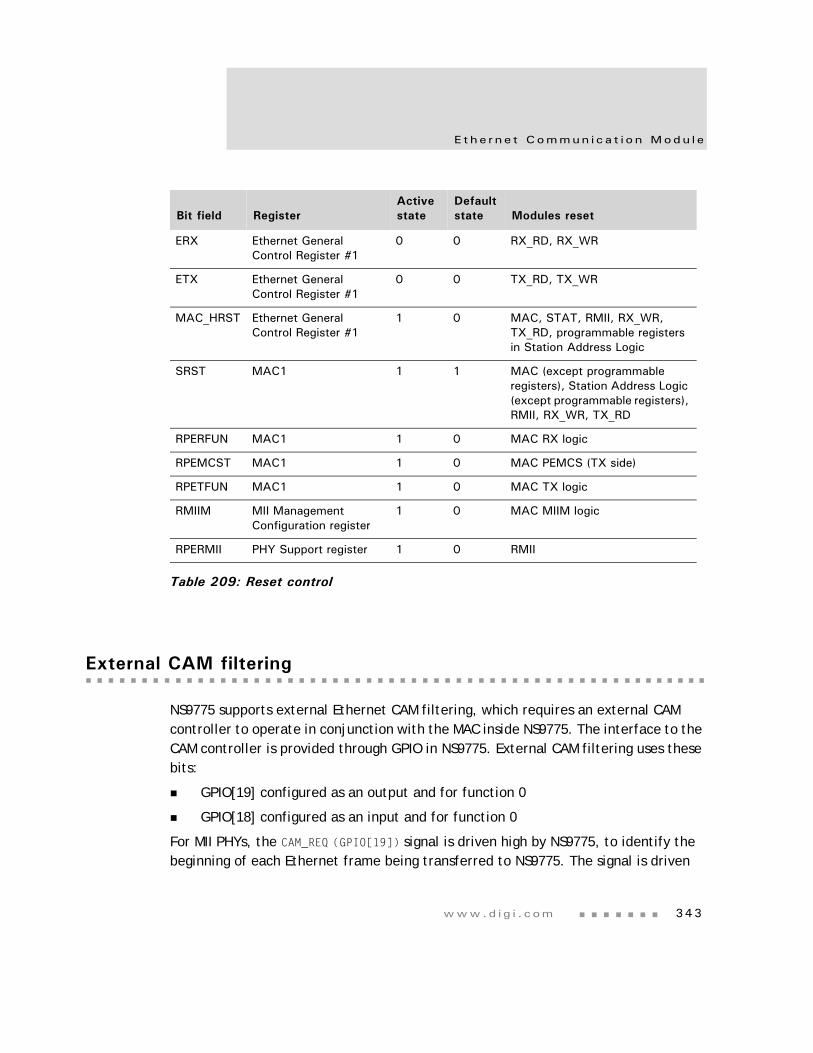
www.d i g i . com 343
E t he r n e t Commun i c a t i o n Modu l e
External CAM filtering
NS9775 supports external Ethernet CAM filtering, which requires an external CAM controller to operate in conjunction with the MAC inside NS9775. The interface to the CAM controller is provided through GPIO in NS9775. External CAM filtering uses these bits:
GPIO[19] configured as an output and for function 0
GPIO[18] configured as an input and for function 0
For MII PHYs, the CAM_REQ (GPIO[19]) signal is driven high by NS9775, to identify the beginning of each Ethernet frame being transferred to NS9775. The signal is driven
Bit field RegisterActive state
Default state Modules reset
ERX Ethernet General Control Register #1
0 0 RX_RD, RX_WR
ETX Ethernet General Control Register #1
0 0 TX_RD, TX_WR
MAC_HRST Ethernet General Control Register #1
1 0 MAC, STAT, RMII, RX_WR, TX_RD, programmable registers in Station Address Logic
SRST MAC1 1 1 MAC (except programmable registers), Station Address Logic (except programmable registers), RMII, RX_WR, TX_RD
RPERFUN MAC1 1 0 MAC RX logic
RPEMCST MAC1 1 0 MAC PEMCS (TX side)
RPETFUN MAC1 1 0 MAC TX logic
RMIIM MII Management Configuration register
1 0 MAC MIIM logic
RPERMII PHY Support register 1 0 RMII
Table 209: Reset control
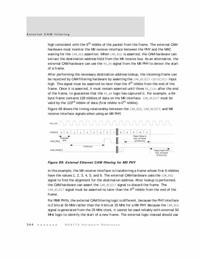
Ex t e r n a l CAM f i l t e r i n g
3 4 4 NS9775 Ha r dwa r e Re f e r ence
high coincident with the 6th nibble of the packet from the frame. The external CAM hardware must monitor the MII receive interface between the PHY and the MAC waiting for the CAM_REQ assertion. When CAM_REQ is asserted, the CAM hardware can extract the destination address field from the MII receive bus. As an alternative, the external CAM hardware can use the RX_DV signal from the MII PHY to detect the start of a frame.
After performing the necessary destination address lookup, the incoming frame can be rejected by CAM filtering hardware by asserting the CAM_REJECT (GPIO[20]) input high. This signal must be asserted no later than the 4th nibble from the end of the frame. Once it is asserted, it must remain asserted until three RX_CLKs after the end of the frame, to guarantee that the RX_WR logic has captured it. For example, a 64-byte frame contains 128 nibbles of data on the MII interface. CAM_REJECT must be valid by the 123rd nibble of data (first nibble is 0th nibble).
Figure 69 shows the timing relationship between the CAM_REQ, CAM_REJECT, and MII receive interface signals when using an MII PHY.
Figure 69: External Ethernet CAM filtering for MII PHY
In this example, the MII receive interface is transferring a frame whose first 6 nibbles have the values 1, 2, 3, 4, 5, and 6. The external CAM hardware uses the CAM_REQ signal to find the alignment for the destination address. After lookup is performed, the CAM hardware can assert the CAM_REJECT signal to discard the frame. The CAM_REJECT signal must be asserted no later than the 4th nibble from the end of the frame.
For RMII PHYs, the external CAM filtering logic is different, because the PHY interface is 2 bits at 50 MHz rather than the 4 bits at 25 MHz for a MII PHY. Because the CAM_REQ signal is generated from the 25 MHz clock, it cannot be used reliably with external 50 MHz logic to identify the start of a new frame. The external logic instead should use
5 D 2 1 4 3 6 5 7 8 9 A B C
Preamble/SFD
Reject Setup toEnd of Packet(4 RXCLKs)
Reject Hold FromEnd of Packet(3 RXCLKs)
5 RXCLKs
RX_CLK
RXD[3:0]
CAM_REQ
CAM_REJECT
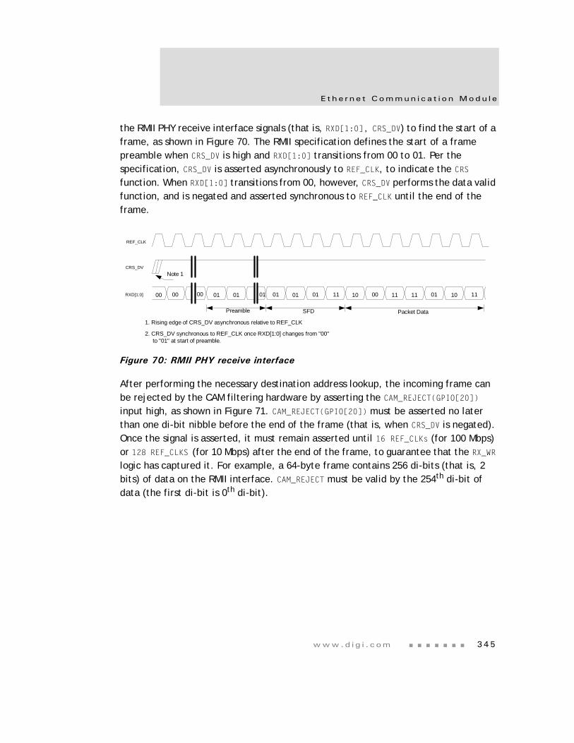
www.d i g i . com 345
E t he r n e t Commun i c a t i o n Modu l e
the RMII PHY receive interface signals (that is, RXD[1:0], CRS_DV) to find the start of a frame, as shown in Figure 70. The RMII specification defines the start of a frame preamble when CRS_DV is high and RXD[1:0] transitions from 00 to 01. Per the specification, CRS_DV is asserted asynchronously to REF_CLK, to indicate the CRS function. When RXD[1:0] transitions from 00, however, CRS_DV performs the data valid function, and is negated and asserted synchronous to REF_CLK until the end of the frame.
Figure 70: RMII PHY receive interface
After performing the necessary destination address lookup, the incoming frame can be rejected by the CAM filtering hardware by asserting the CAM_REJECT(GPIO[20]) input high, as shown in Figure 71. CAM_REJECT(GPIO[20]) must be asserted no later than one di-bit nibble before the end of the frame (that is, when CRS_DV is negated). Once the signal is asserted, it must remain asserted until 16 REF_CLKs (for 100 Mbps) or 128 REF_CLKS (for 10 Mbps) after the end of the frame, to guarantee that the RX_WR logic has captured it. For example, a 64-byte frame contains 256 di-bits (that is, 2 bits) of data on the RMII interface. CAM_REJECT must be valid by the 254th di-bit of data (the first di-bit is 0th di-bit).
00 01 01 01 01 11 10 00 11 11
Preamble
REF_CLK
RXD[1:0] 00 00 01 01 01 10 11
CRS_DV
SFD Packet Data
Note 1
1. Rising edge of CRS_DV asynchronous relative to REF_CLK
2. CRS_DV synchronous to REF_CLK once RXD[1:0] changes from "00"to "01" at start of preamble.
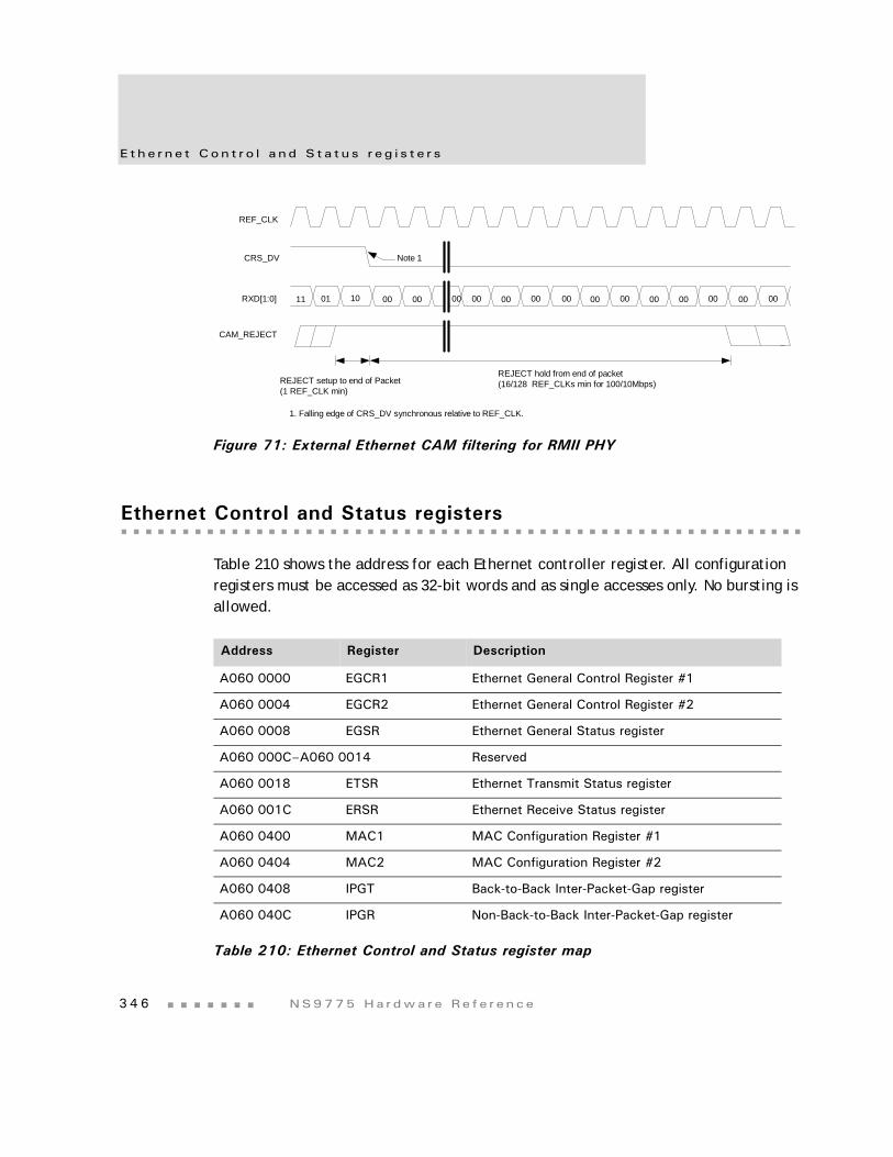
E t he r n e t Con t r o l a nd S t a t u s r eg i s t e r s
3 4 6 NS9775 Ha r dwa r e Re f e r ence
Figure 71: External Ethernet CAM filtering for RMII PHY
Ethernet Control and Status registers
Table 210 shows the address for each Ethernet controller register. All configuration registers must be accessed as 32-bit words and as single accesses only. No bursting is allowed.
11 00 00 00 00 00 00 00 00 00
REF_CLK
RXD[1:0] 01 10 00 00 00 00 00
CRS_DV Note 1
1. Falling edge of CRS_DV synchronous relative to REF_CLK.
CAM_REJECT
REJECT setup to end of Packet(1 REF_CLK min)
REJECT hold from end of packet(16/128 REF_CLKs min for 100/10Mbps)
Address Register Description
A060 0000 EGCR1 Ethernet General Control Register #1
A060 0004 EGCR2 Ethernet General Control Register #2
A060 0008 EGSR Ethernet General Status register
A060 000C–A060 0014 Reserved
A060 0018 ETSR Ethernet Transmit Status register
A060 001C ERSR Ethernet Receive Status register
A060 0400 MAC1 MAC Configuration Register #1
A060 0404 MAC2 MAC Configuration Register #2
A060 0408 IPGT Back-to-Back Inter-Packet-Gap register
A060 040C IPGR Non-Back-to-Back Inter-Packet-Gap register
Table 210: Ethernet Control and Status register map
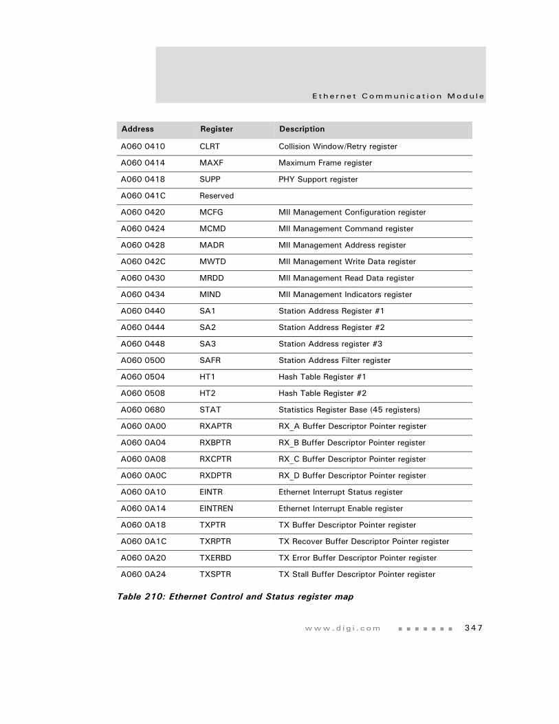
www.d i g i . com 347
E t he r n e t Commun i c a t i o n Modu l e
A060 0410 CLRT Collision Window/Retry register
A060 0414 MAXF Maximum Frame register
A060 0418 SUPP PHY Support register
A060 041C Reserved
A060 0420 MCFG MII Management Configuration register
A060 0424 MCMD MII Management Command register
A060 0428 MADR MII Management Address register
A060 042C MWTD MII Management Write Data register
A060 0430 MRDD MII Management Read Data register
A060 0434 MIND MII Management Indicators register
A060 0440 SA1 Station Address Register #1
A060 0444 SA2 Station Address Register #2
A060 0448 SA3 Station Address register #3
A060 0500 SAFR Station Address Filter register
A060 0504 HT1 Hash Table Register #1
A060 0508 HT2 Hash Table Register #2
A060 0680 STAT Statistics Register Base (45 registers)
A060 0A00 RXAPTR RX_A Buffer Descriptor Pointer register
A060 0A04 RXBPTR RX_B Buffer Descriptor Pointer register
A060 0A08 RXCPTR RX_C Buffer Descriptor Pointer register
A060 0A0C RXDPTR RX_D Buffer Descriptor Pointer register
A060 0A10 EINTR Ethernet Interrupt Status register
A060 0A14 EINTREN Ethernet Interrupt Enable register
A060 0A18 TXPTR TX Buffer Descriptor Pointer register
A060 0A1C TXRPTR TX Recover Buffer Descriptor Pointer register
A060 0A20 TXERBD TX Error Buffer Descriptor Pointer register
A060 0A24 TXSPTR TX Stall Buffer Descriptor Pointer register
Address Register Description
Table 210: Ethernet Control and Status register map
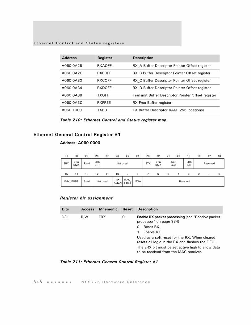
E t he r n e t Con t r o l a nd S t a t u s r eg i s t e r s
3 4 8 NS9775 Ha r dwa r e Re f e r ence
Ethernet General Control Register #1
Address: A060 0000
Register bit assignment
A060 0A28 RXAOFF RX_A Buffer Descriptor Pointer Offset register
A060 0A2C RXBOFF RX_B Buffer Descriptor Pointer Offset register
A060 0A30 RXCOFF RX_C Buffer Descriptor Pointer Offset register
A060 0A34 RXDOFF RX_D Buffer Descriptor Pointer Offset register
A060 0A38 TXOFF Transmit Buffer Descriptor Pointer Offset register
A060 0A3C RXFREE RX Free Buffer register
A060 1000 TXBD TX Buffer Descriptor RAM (256 locations)
Address Register Description
Table 210: Ethernet Control and Status register map
Bits Access Mnemonic Reset Description
D31 R/W ERX 0 Enable RX packet processing (see "Receive packet processor" on page 334)0 Reset RX1 Enable RXUsed as a soft reset for the RX. When cleared, resets all logic in the RX and flushes the FIFO.The ERX bit must be set active high to allow data to be received from the MAC receiver.
Table 211: Ethernet General Control Register #1
RXALIGN
MAC_HRST ITXA
13 12 11 10 9 8 7 6 5 4 3 2 1 015 14
PHY_MODE
31 29 28 27 26 25 24 23 22 21 20 19 18 17 1630
Rsvd ERXSHT Not used ETX ETX
DMANotused
ERXINITERX ERX
DMA Reserved
ReservedNot usedRsvd
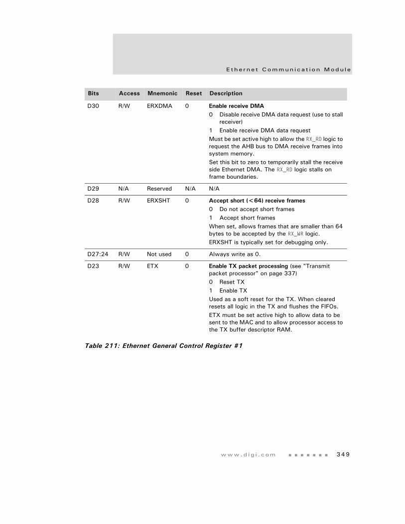
www.d i g i . com 349
E t he r n e t Commun i c a t i o n Modu l e
D30 R/W ERXDMA 0 Enable receive DMA0 Disable receive DMA data request (use to stall
receiver)1 Enable receive DMA data requestMust be set active high to allow the RX_RD logic to request the AHB bus to DMA receive frames into system memory. Set this bit to zero to temporarily stall the receive side Ethernet DMA. The RX_RD logic stalls on frame boundaries.
D29 N/A Reserved N/A N/A
D28 R/W ERXSHT 0 Accept short (<64) receive frames0 Do not accept short frames1 Accept short framesWhen set, allows frames that are smaller than 64 bytes to be accepted by the RX_WR logic. ERXSHT is typically set for debugging only.
D27:24 R/W Not used 0 Always write as 0.
D23 R/W ETX 0 Enable TX packet processing (see "Transmit packet processor" on page 337)0 Reset TX1 Enable TXUsed as a soft reset for the TX. When cleared resets all logic in the TX and flushes the FIFOs. ETX must be set active high to allow data to be sent to the MAC and to allow processor access to the TX buffer descriptor RAM.
Bits Access Mnemonic Reset Description
Table 211: Ethernet General Control Register #1
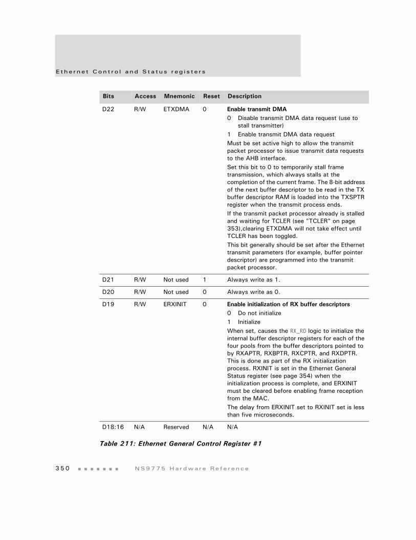
E t he r n e t Con t r o l a nd S t a t u s r eg i s t e r s
3 5 0 NS9775 Ha r dwa r e Re f e r ence
D22 R/W ETXDMA 0 Enable transmit DMA0 Disable transmit DMA data request (use to
stall transmitter)1 Enable transmit DMA data requestMust be set active high to allow the transmit packet processor to issue transmit data requests to the AHB interface. Set this bit to 0 to temporarily stall frame transmission, which always stalls at the completion of the current frame. The 8-bit address of the next buffer descriptor to be read in the TX buffer descriptor RAM is loaded into the TXSPTR register when the transmit process ends. If the transmit packet processor already is stalled and waiting for TCLER (see "TCLER" on page 353),clearing ETXDMA will not take effect until TCLER has been toggled.This bit generally should be set after the Ethernet transmit parameters (for example, buffer pointer descriptor) are programmed into the transmit packet processor.
D21 R/W Not used 1 Always write as 1.
D20 R/W Not used 0 Always write as 0.
D19 R/W ERXINIT 0 Enable initialization of RX buffer descriptors0 Do not initialize1 InitializeWhen set, causes the RX_RD logic to initialize the internal buffer descriptor registers for each of the four pools from the buffer descriptors pointed to by RXAPTR, RXBPTR, RXCPTR, and RXDPTR. This is done as part of the RX initialization process. RXINIT is set in the Ethernet General Status register (see page 354) when the initialization process is complete, and ERXINIT must be cleared before enabling frame reception from the MAC. The delay from ERXINIT set to RXINIT set is less than five microseconds.
D18:16 N/A Reserved N/A N/A
Bits Access Mnemonic Reset Description
Table 211: Ethernet General Control Register #1
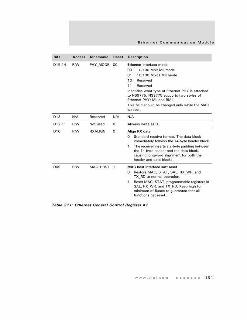
www.d i g i . com 351
E t he r n e t Commun i c a t i o n Modu l e
D15:14 R/W PHY_MODE 00 Ethernet interface mode00 10/100 Mbit MII mode01 10/100 Mbit RMII mode10 Reserved11 ReservedIdentifies what type of Ethernet PHY is attached to NS9775. NS9775 supports two styles of Ethernet PHY: MII and RMII. This field should be changed only while the MAC is reset.
D13 N/A Reserved N/A N/A
D12:11 R/W Not used 0 Always write as 0.
D10 R/W RXALIGN 0 Align RX data0 Standard receive format. The data block
immediately follows the 14-byte header block.1 The receiver inserts a 2-byte padding between
the 14-byte header and the data block, causing longword alignment for both the header and data blocks.
D09 R/W MAC_HRST 1 MAC host interface soft reset0 Restore MAC, STAT, SAL, RX_WR, and
TX_RD to normal operation.1 Reset MAC, STAT, programmable registers in
SAL, RX_WR, and TX_RD. Keep high for minimum of 5μsec to guarantee that all functions get reset.
Bits Access Mnemonic Reset Description
Table 211: Ethernet General Control Register #1
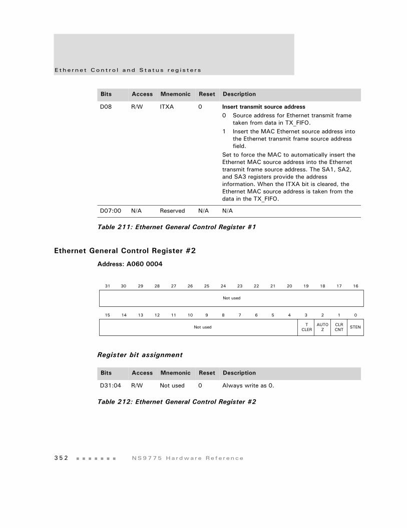
E t he r n e t Con t r o l a nd S t a t u s r eg i s t e r s
3 5 2 NS9775 Ha r dwa r e Re f e r ence
Ethernet General Control Register #2
Address: A060 0004
Register bit assignment
D08 R/W ITXA 0 Insert transmit source address0 Source address for Ethernet transmit frame
taken from data in TX_FIFO.1 Insert the MAC Ethernet source address into
the Ethernet transmit frame source address field.
Set to force the MAC to automatically insert the Ethernet MAC source address into the Ethernet transmit frame source address. The SA1, SA2, and SA3 registers provide the address information. When the ITXA bit is cleared, the Ethernet MAC source address is taken from the data in the TX_FIFO.
D07:00 N/A Reserved N/A N/A
Bits Access Mnemonic Reset Description
Table 211: Ethernet General Control Register #1
Bits Access Mnemonic Reset Description
D31:04 R/W Not used 0 Always write as 0.
Table 212: Ethernet General Control Register #2
Not used
TCLER STEN
13 12 11 10 9 8 7 6 5 4 3 2 1 015 14
31 29 28 27 26 25 24 23 22 21 20 19 18 17 1630
Not used AUTOZ
CLRCNT
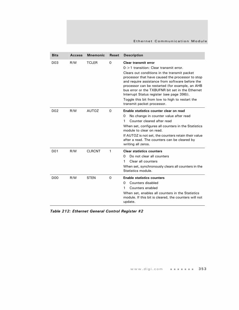
www.d i g i . com 353
E t he r n e t Commun i c a t i o n Modu l e
D03 R/W TCLER 0 Clear transmit error0->1 transition: Clear transmit error.Clears out conditions in the transmit packet processor that have caused the processor to stop and require assistance from software before the processor can be restarted (for example, an AHB bus error or the TXBUFNR bit set in the Ethernet Interrupt Status register (see page 396)). Toggle this bit from low to high to restart the transmit packet processor.
D02 R/W AUTOZ 0 Enable statistics counter clear on read0 No change in counter value after read1 Counter cleared after readWhen set, configures all counters in the Statistics module to clear on read. If AUTOZ is not set, the counters retain their value after a read. The counters can be cleared by writing all zeros.
D01 R/W CLRCNT 1 Clear statistics counters0 Do not clear all counters1 Clear all countersWhen set, synchronously clears all counters in the Statistics module.
D00 R/W STEN 0 Enable statistics counters0 Counters disabled1 Counters enabledWhen set, enables all counters in the Statistics module. If this bit is cleared, the counters will not update.
Bits Access Mnemonic Reset Description
Table 212: Ethernet General Control Register #2
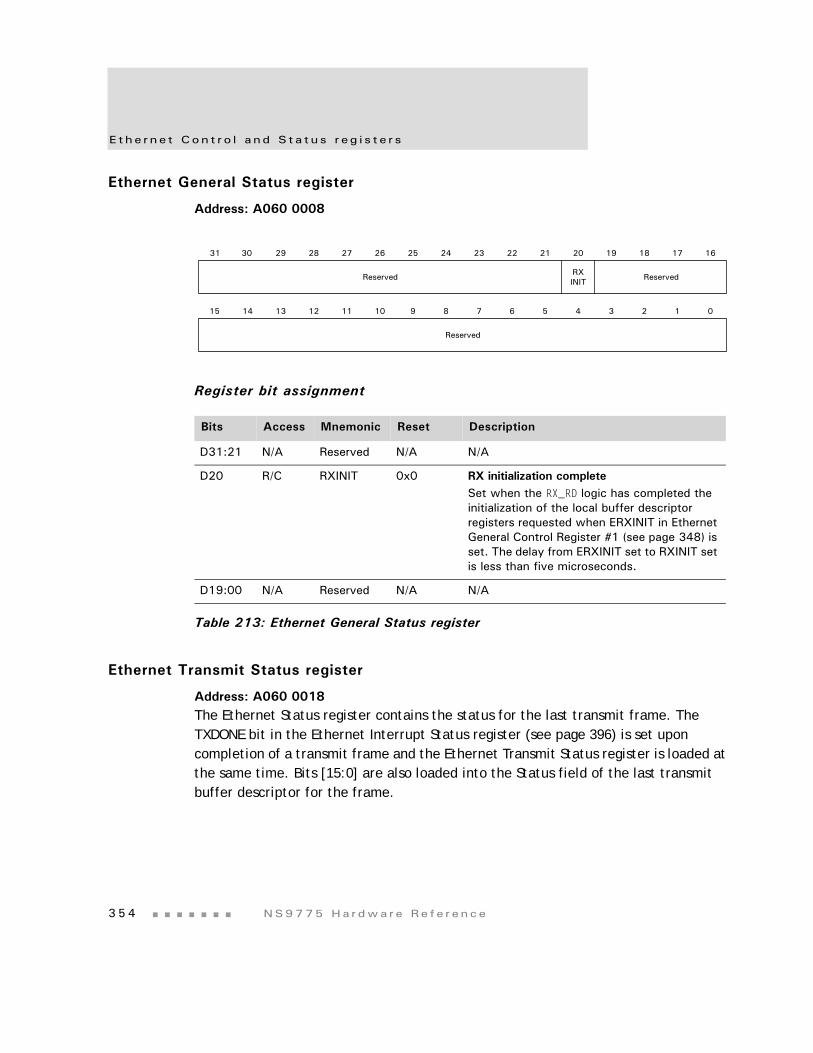
E t he r n e t Con t r o l a nd S t a t u s r eg i s t e r s
3 5 4 NS9775 Ha r dwa r e Re f e r ence
Ethernet General Status register
Address: A060 0008
Register bit assignment
Ethernet Transmit Status register
Address: A060 0018The Ethernet Status register contains the status for the last transmit frame. The TXDONE bit in the Ethernet Interrupt Status register (see page 396) is set upon completion of a transmit frame and the Ethernet Transmit Status register is loaded at the same time. Bits [15:0] are also loaded into the Status field of the last transmit buffer descriptor for the frame.
Bits Access Mnemonic Reset Description
D31:21 N/A Reserved N/A N/A
D20 R/C RXINIT 0x0 RX initialization completeSet when the RX_RD logic has completed the initialization of the local buffer descriptor registers requested when ERXINIT in Ethernet General Control Register #1 (see page 348) is set. The delay from ERXINIT set to RXINIT set is less than five microseconds.
D19:00 N/A Reserved N/A N/A
Table 213: Ethernet General Status register
Reserved
13 12 11 10 9 8 7 6 5 4 3 2 1 015 14
31 29 28 27 26 25 24 23 22 21 20 19 18 17 1630
Reserved
RXINIT Reserved
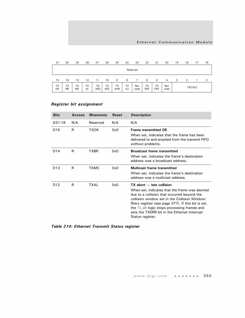
www.d i g i . com 355
E t he r n e t Commun i c a t i o n Modu l e
Register bit assignment
Bits Access Mnemonic Reset Description
D31:16 N/A Reserved N/A N/A
D15 R TXOK 0x0 Frame transmitted OKWhen set, indicates that the frame has been delivered to and emptied from the transmit FIFO without problems.
D14 R TXBR 0x0 Broadcast frame transmittedWhen set, indicates the frame’s destination address was a broadcast address.
D13 R TXMC 0x0 Multicast frame transmittedWhen set, indicates the frame’s destination address was a multicast address.
D12 R TXAL 0x0 TX abort — late collisionWhen set, indicates that the frame was aborted due to a collision that occurred beyond the collision window set in the Collision Window/Retry register (see page 377). If this bit is set, the TX_WR logic stops processing frames and sets the TXERR bit in the Ethernet Interrupt Status register.
Table 214: Ethernet Transmit Status register
Reserved
13 12 11 10 9 8 7 6 5 4 3 2 1 015 14
31 29 28 27 26 25 24 23 22 21 20 19 18 17 1630
Notused
TXDEF
TXCRC
Notused TXCOLCTX
OKTXBR
TXMC
TXAL
TXAED
TXAEC
TXAUR
TXAJ
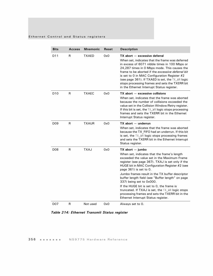
E t he r n e t Con t r o l a nd S t a t u s r eg i s t e r s
3 5 6 NS9775 Ha r dwa r e Re f e r ence
D11 R TXAED 0x0 TX abort — excessive deferralWhen set, indicates that the frame was deferred in excess of 6071 nibble times in 100 Mbps or 24,287 times in 0 Mbps mode. This causes the frame to be aborted if the excessive deferral bit is set to 0 in MAC Configuration Register #2 (see page 361). If TXAED is set, the TX_WR logic stops processing frames and sets the TXERR bit in the Ethernet Interrupt Status register.
D10 R TXAEC 0x0 TX abort — excessive collisionsWhen set, indicates that the frame was aborted because the number of collisions exceeded the value set in the Collision Window/Retry register. If this bit is set, the TX_WR logic stops processing frames and sets the TXERR bit in the Ethernet Interrupt Status register.
D09 R TXAUR 0x0 TX abort — underrunWhen set, indicates that the frame was aborted because the TX_FIFO had an underrun. If this bit is set, the TX_WR logic stops processing frames and sets the TXERR bit in the Ethernet Interrupt Status register.
D08 R TXAJ 0x0 TX abort — jumboWhen set, indicates that the frame’s length exceeded the value set in the Maximum Frame register (see page 367). TXAJ is set only if the HUGE bit in MAC Configuration Register #2 (see page 361) is set to 0.Jumbo frames result in the TX buffer descriptor buffer length field (see "Buffer length" on page 337) being set to 0x000.If the HUGE bit is set to 0, the frame is truncated. If TXAJ is set, the TX_WR logic stops processing frames and sets the TXERR bit in the Ethernet Interrupt Status register.
D07 R Not used 0x0 Always set to 0.
Bits Access Mnemonic Reset Description
Table 214: Ethernet Transmit Status register
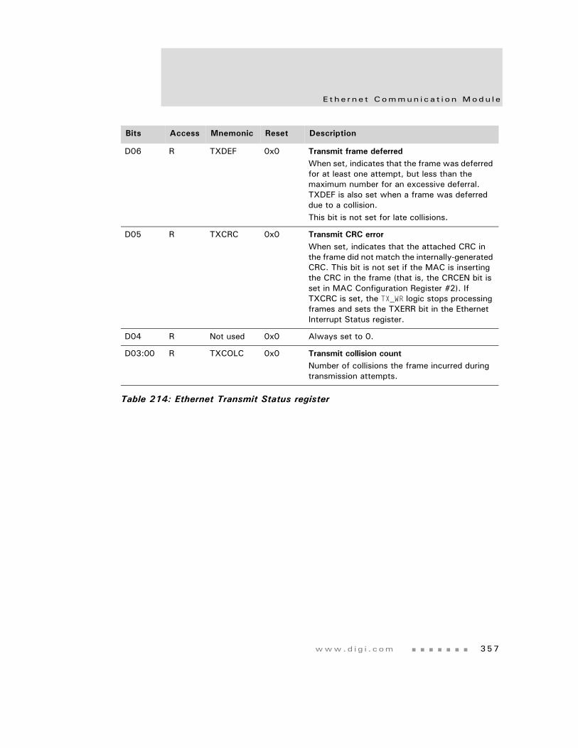
www.d i g i . com 357
E t he r n e t Commun i c a t i o n Modu l e
D06 R TXDEF 0x0 Transmit frame deferredWhen set, indicates that the frame was deferred for at least one attempt, but less than the maximum number for an excessive deferral. TXDEF is also set when a frame was deferred due to a collision. This bit is not set for late collisions.
D05 R TXCRC 0x0 Transmit CRC errorWhen set, indicates that the attached CRC in the frame did not match the internally-generated CRC. This bit is not set if the MAC is inserting the CRC in the frame (that is, the CRCEN bit is set in MAC Configuration Register #2). If TXCRC is set, the TX_WR logic stops processing frames and sets the TXERR bit in the Ethernet Interrupt Status register.
D04 R Not used 0x0 Always set to 0.
D03:00 R TXCOLC 0x0 Transmit collision countNumber of collisions the frame incurred during transmission attempts.
Bits Access Mnemonic Reset Description
Table 214: Ethernet Transmit Status register
E t he r n e t Con t r o l a nd S t a t u s r eg i s t e r s
3 5 8 NS9775 Ha r dwa r e Re f e r ence
Ethernet Receive Status register
Address: A060 001CThe Ethernet Receive Status register contains the status for the last completed receive frame. The RXBR bit in the Ethernet Interrupt Status register (see page 396) is set whenever a receive frame is completed and the Ethernet Receive Status register is loaded at the same time. Bits [15:0] are also loaded into the status field of the receive buffer descriptor used for the frame.
Register bit assignment
Bits Access Mnemonic Reset Description
D31:27 N/A Reserved N/A N/A
D26:16 R RXSIZE 0x000 Receive frame size in bytesLength of the received frame, in bytes.
D15 R RXCE 0x0 Receive carrier event previously seenWhen set, indicates that a carrier event activity (an activity on the receive channel that does not result in a frame receive attempt being made) was found at some point since the last receive statistics. A carrier event results when the interface signals to the PHY have the following values:
MRXER = 1MRXDV = 0RXD = 0xE
The event is being reported with this frame, although it is not associated with the frame.
Table 215: Ethernet Receive Status register
13 12 11 10 9 8 7 6 5 4 3 2 1 015 14
31 29 28 27 26 25 24 23 22 21 20 19 18 17 1630
ReservedRXCE RXDV RXOK RXBR RXMC Rsvd RXDR
Reserved RXSIZE
www.d i g i . com 359
E t he r n e t Commun i c a t i o n Modu l e
D14 R RXDV 0x0 Receive data violation event previously seenSet when the last receive event was not long enough to be a valid frame.
D13 R RXOK 0x0 Receive frame OKSet when the frame had a valid CRC and no symbol errors.
D12 R RXBR 0x0 Receive broadcast frameSet when the frame has a valid broadcast address.
D11 R RXMC 0x0 Receive multicast frameSet when the frame has a valid multicast address.
D10 N/A Reserved N/A N/A
D09 R RXDR 0x0 Receive frame has dribble bitsSet when an additional 1–7 bits are received after the end of the frame.
Note: Ignore this bit with RMII applications.
D08:00 N/A Reserved N/A N/A
Bits Access Mnemonic Reset Description
Table 215: Ethernet Receive Status register
E t he r n e t Con t r o l a nd S t a t u s r eg i s t e r s
3 6 0 NS9775 Ha r dwa r e Re f e r ence
MAC Configuration Register #1
Address: A060 0400MAC Configuration Register #1 provides bits that control functionality within the Ethernet MAC block.
Register bit assignment
Bits Access Mnemonic Reset Description
D31:16 N/A Reserved N/A N/A
D15 R/W SRST 1 Soft resetSet this bit to 1 to reset the RX_WR, TX_RD, MAC (except host interface), SAL (except host interface), and RMII modules.
D14 R/W Not used 0 Always write as 0.
D13:12 N/A Reserved N/A N/A
D11 N/A Not used 0 Always write as 0.
D10 R/W RPERFUN 0 Reset PERFUNSet this bit to 1 to put the MAC receive logic into reset.
D09 R/W RPEMCST 0 Reset PEMCS/TXSet this bit to 1 to put the MAC control sublayer/transmit domain logic into reset.
D08 R/W RPETFUN 0 Reset PETFUNSet this bit to 1 to put the MAC transmit logic into reset.
D07:05 N/A Reserved N/A N/A
Table 216: MAC Configuration Register #1
Reserved
13 12 11 10 9 8 7 6 5 4 3 2 1 015 14
31 29 28 27 26 25 24 23 22 21 20 19 18 17 1630
ReservedSRST RPERFUN
RPEMCST
RPETFUNReserved LOOP
BK RXENNotused Not usedNot
used
www.d i g i . com 361
E t he r n e t Commun i c a t i o n Modu l e
MAC Configuration Register #2
Address: A060 0404MAC Configuration Register #2 provides additional bits that control functionality within the Ethernet MAC block.
Register bit assignment
D04 R/W LOOPBK 0 Internal loopbackSet this bit to 1 to cause the MAC transmit interface to be internally looped back to the MAC receive interface. Clearing this bit results in normal operation.
D03:01 R/W Not used 0 Always write as 0.
D00 R/W RXEN 0 Receive enableSet this bit to 1 to allow the MAC receiver to receive frames.
Bits Access Mnemonic Reset Description
Table 216: MAC Configuration Register #1
Bits Access Mnemonic Reset Definition
D31:15 N/A Reserved N/A N/A
Table 217: MAC Configuration Register #2
Reserved
13 12 11 10 9 8 7 6 5 4 3 2 1 015 14
31 29 28 27 26 25 24 23 22 21 20 19 18 17 1630
ReservedRsvd EDEFER LONGP PUREP CRCEN Not
used HUGE Notused FULLDNot
used NOBO AUTOP VLANP PADEN
E t he r n e t Con t r o l a nd S t a t u s r eg i s t e r s
3 6 2 NS9775 Ha r dwa r e Re f e r ence
D14 R/W EDEFER 0 Excess deferral0 The MAC aborts when the excessive deferral
limit is reached (that is, 6071 nibble times in 100 Mbps mode or 24,287 bit times in 10 Mbps mode).
1 Enables the MAC to defer to carrier indefinitely, as per the 802.3u standard.
D13 R/W Not used 0 Always write to 0.
D12 R/W NOBO 0 No backoffWhen this bit is set to 1, the MAC immediately retransmits following a collision, rather than using the binary exponential backoff algorithm (as specified in the 802.3u standard).
D11:10 N/A Reserved N/A N/A
D09 R/W LONGP 0 Long preamble enforcement0 Allows any length preamble (as defined in the
802.3u standard).1 The MAC allows only receive frames that
contain preamble fields less than 12 bytes in length.
D08 R/W PUREP 0 Pure preamble enforcement0 No preamble checking is performed1 The MAC certifies the content of the preamble
to ensure that it contains 0x55 and is error-free.
D07 R/W AUTOP 0 Auto detect pad enableWhen set to 1, this bit causes the MAC to detect automatically the type of transmit frame, either tagged or untagged, by comparing the two octets following the source address with the 0x8100 VLAN protect ID and pad accordingly.
Note: This bit is ignored if PADEN is set to 0.
See "PAD operation table for transmit frames" on page 364 for more information.
Bits Access Mnemonic Reset Definition
Table 217: MAC Configuration Register #2
www.d i g i . com 363
E t he r n e t Commun i c a t i o n Modu l e
D06 R/W VLANP 0 VLAN pad enableSet to 1 to have the MAC pad all short transmit frames to 64 bytes and to append a valid CRC. This bit is used in conjunction with auto detect pad enable (AUTOP) and pad/CRC enable (PADEN). See "PAD operation table for transmit frames" on page 364.
Note: This bit is ignored if PADEN is set to 0.
D05 R/W PADEN 0 Pad/CRC enable0 Short transmit frames not padded.1 The MAC pads all short transmit frames.This bit is used in conjunction with auto detect pad enable (AUTOP) and VLAN pad enable (VLANP). See "PAD operation table for transmit frames" on page 364.
D04 R/W CRCEN 0 CRC enable0 Transmit frames presented to the MAC
contain a CRC.1 Append a CRC to every transmit frame,
whether padding is required or not. CRCEN must be set if PADEN is set to 1.
D03 R/W Not used 0 Always write as 0.
D02 R/W HUGE 0 Huge frame enable0 Transmit and receive frames are limited to the
MAXF value in the Maximum Frame register (see "Maximum Frame register" on page 367).
1 Frames of any length are transmitted and received.
D01 R/W Not used 0 Always write as 0.
D00 R/W FULLD 0 Full-duplex0 The MAC operates in half-duplex mode.1 The MAC operates in full-duplex mode.
Bits Access Mnemonic Reset Definition
Table 217: MAC Configuration Register #2
E t he r n e t Con t r o l a nd S t a t u s r eg i s t e r s
3 6 4 NS9775 Ha r dwa r e Re f e r ence
PAD operation table for transmit frames
Back-to-Back Inter-Packet-Gap register
Address: A060 0408
Register bit assignment
Type AUTOP VLANP PADEN Action
Any X X 0 No pad; check CRC
Any 0 0 1 Pad to 60 bytes; append CRC
Any X 1 1 Pad to 64 bytes; append CRC
Any 1 0 1 If untagged, pad to 60 bytes; append CRCIf VLAN tagged, pad to 64 bytes; append CRC
Bits Access Mnemonic Reset Description
D31:07 N/A Reserved N/A N/A
Table 218: Back-to-Back Inter-Packet-Gap register
Reserved
IPGT
13 12 11 10 9 8 7 6 5 4 3 2 1 015 14
31 29 28 27 26 25 24 23 22 21 20 19 18 17 1630
Reserved
www.d i g i . com 365
E t he r n e t Commun i c a t i o n Modu l e
Non Back-to-Back Inter-Packet-Gap register
Address: A060 040C
Register bit assignment
D06:00 R/W IPGT 0x00 Back-to-back inter-packet-gapProgrammable field that indicates the nibble time offset of the minimum period between the end of any transmitted frame to the beginning of the next frame. Full-duplex mode
Register value should be the appropriate period in nibble times minus 3.
Recommended setting is 0x15 (21d), which represents the minimum IPG of 0.96 uS (in 100 Mbps) or 9.6uS (in 10 Mbps).
Half-duplex mode
Register value should be the appropriate period in nibble times minus 6.
Recommended setting is 0x12 (18d), which represents the minimum IPG of 0.96 uS (in 100 Mbps) or 9.6 uS (in 10 Mbps).
Bits Access Mnemonic Reset Description
Table 218: Back-to-Back Inter-Packet-Gap register
Bits Access Mnemonic Reset Description
D31:15 N/A Reserved N/A N/A
Table 219: Non Back-to-Back Inter-Packet-Gap register
Reserved
IPGR2
13 12 11 10 9 8 7 6 5 4 3 2 1 015 14
31 29 28 27 26 25 24 23 22 21 20 19 18 17 1630
IPGR1Rsvd Rsvd
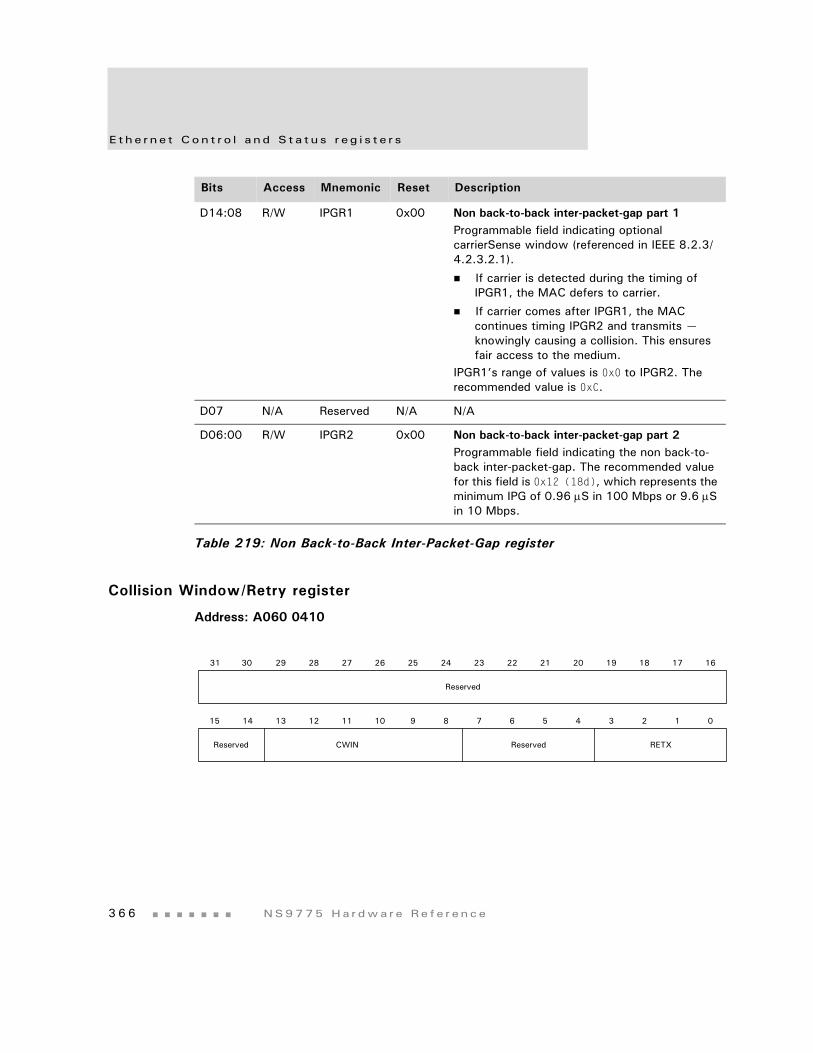
E t he r n e t Con t r o l a nd S t a t u s r eg i s t e r s
3 6 6 NS9775 Ha r dwa r e Re f e r ence
Collision Window/Retry register
Address: A060 0410
D14:08 R/W IPGR1 0x00 Non back-to-back inter-packet-gap part 1Programmable field indicating optional carrierSense window (referenced in IEEE 8.2.3/4.2.3.2.1).
If carrier is detected during the timing of IPGR1, the MAC defers to carrier.
If carrier comes after IPGR1, the MAC continues timing IPGR2 and transmits — knowingly causing a collision. This ensures fair access to the medium.
IPGR1’s range of values is 0x0 to IPGR2. The recommended value is 0xC.
D07 N/A Reserved N/A N/A
D06:00 R/W IPGR2 0x00 Non back-to-back inter-packet-gap part 2Programmable field indicating the non back-to-back inter-packet-gap. The recommended value for this field is 0x12 (18d), which represents the minimum IPG of 0.96 μS in 100 Mbps or 9.6 μS in 10 Mbps.
Bits Access Mnemonic Reset Description
Table 219: Non Back-to-Back Inter-Packet-Gap register
Reserved
RETX
13 12 11 10 9 8 7 6 5 4 3 2 1 015 14
31 29 28 27 26 25 24 23 22 21 20 19 18 17 1630
CWINReserved Reserved
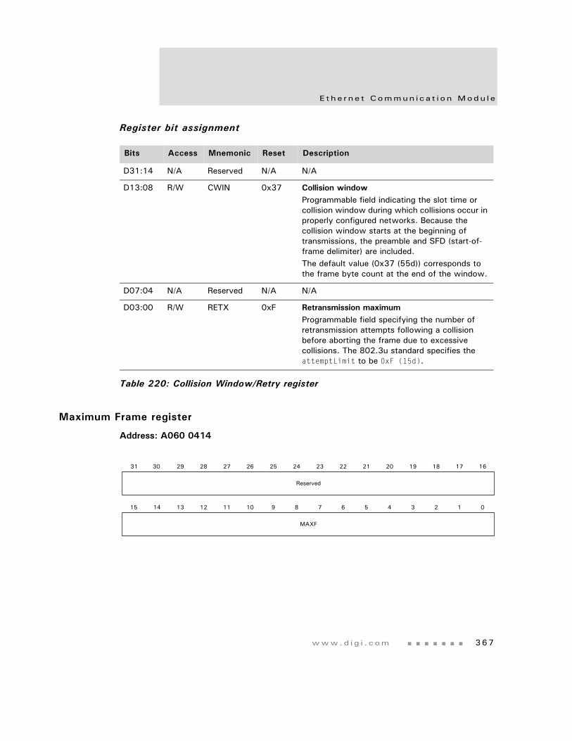
www.d i g i . com 367
E t he r n e t Commun i c a t i o n Modu l e
Register bit assignment
Maximum Frame register
Address: A060 0414
Bits Access Mnemonic Reset Description
D31:14 N/A Reserved N/A N/A
D13:08 R/W CWIN 0x37 Collision windowProgrammable field indicating the slot time or collision window during which collisions occur in properly configured networks. Because the collision window starts at the beginning of transmissions, the preamble and SFD (start-of-frame delimiter) are included. The default value (0x37 (55d)) corresponds to the frame byte count at the end of the window.
D07:04 N/A Reserved N/A N/A
D03:00 R/W RETX 0xF Retransmission maximumProgrammable field specifying the number of retransmission attempts following a collision before aborting the frame due to excessive collisions. The 802.3u standard specifies the attemptLimit to be 0xF (15d).
Table 220: Collision Window/Retry register
Reserved
13 12 11 10 9 8 7 6 5 4 3 2 1 015 14
31 29 28 27 26 25 24 23 22 21 20 19 18 17 1630
MAXF
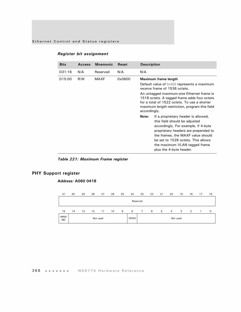
E t he r n e t Con t r o l a nd S t a t u s r eg i s t e r s
3 6 8 NS9775 Ha r dwa r e Re f e r ence
Register bit assignment
PHY Support register
Address: A060 0418
Bits Access Mnemonic Reset Description
D31:16 N/A Reserved N/A N/A
D15:00 R/W MAXF 0x0600 Maximum frame lengthDefault value of 0x600 represents a maximum receive frame of 1536 octets. An untagged maximum-size Ethernet frame is 1518 octets. A tagged frame adds four octets for a total of 1522 octets. To use a shorter maximum length restriction, program this field accordingly.
Note: If a proprietary header is allowed, this field should be adjusted accordingly. For example, if 4-byte proprietary headers are prepended to the frames, the MAXF value should be set to 1526 octets. This allows the maximum VLAN tagged frame plus the 4-byte header.
Table 221: Maximum Frame register
Reserved
13 12 11 10 9 8 7 6 5 4 3 2 1 015 14
31 29 28 27 26 25 24 23 22 21 20 19 18 17 1630
RPERMII Not used SPEED Not used
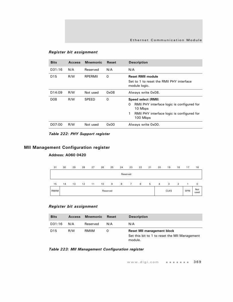
www.d i g i . com 369
E t he r n e t Commun i c a t i o n Modu l e
Register bit assignment
MII Management Configuration register
Address: A060 0420
Register bit assignment
Bits Access Mnemonic Reset Description
D31:16 N/A Reserved N/A N/A
D15 R/W RPERMII 0 Reset RMII moduleSet to 1 to reset the RMII PHY interface module logic.
D14:09 R/W Not used 0x08 Always write 0x08.
D08 R/W SPEED 0 Speed select (RMII)0 RMII PHY interface logic is configured for
10 Mbps1 RMII PHY interface logic is configured for
100 Mbps
D07:00 R/W Not used 0x00 Always write 0x00.
Table 222: PHY Support register
Bits Access Mnemonic Reset Description
D31:16 N/A Reserved N/A N/A
D15 R/W RMIIM 0 Reset MII management blockSet this bit to 1 to reset the MII Management module.
Table 223: MII Management Configuration register
Reserved
Notused
13 12 11 10 9 8 7 6 5 4 3 2 1 015 14
31 29 28 27 26 25 24 23 22 21 20 19 18 17 1630
Reserved CLKS SPRERMIIM
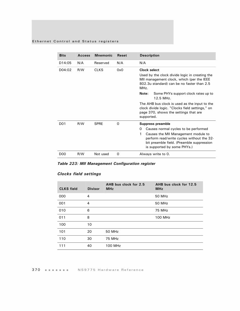
E t he r n e t Con t r o l a nd S t a t u s r eg i s t e r s
3 7 0 NS9775 Ha r dwa r e Re f e r ence
Clocks field settings
D14:05 N/A Reserved N/A N/A
D04:02 R/W CLKS 0x0 Clock selectUsed by the clock divide logic in creating the MII management clock, which (per the IEEE 802.3u standard) can be no faster than 2.5 MHz.
Note: Some PHYs support clock rates up to 12.5 MHz.
The AHB bus clock is used as the input to the clock divide logic. "Clocks field settings," on page 370, shows the settings that are supported.
D01 R/W SPRE 0 Suppress preamble0 Causes normal cycles to be performed1 Causes the MII Management module to
perform read/write cycles without the 32-bit preamble field. (Preamble suppression is supported by some PHYs.)
D00 R/W Not used 0 Always write to 0.
CLKS field DivisorAHB bus clock for 2.5 MHz
AHB bus clock for 12.5 MHz
000 4 50 MHz
001 4 50 MHz
010 6 75 MHz
011 8 100 MHz
100 10
101 20 50 MHz
110 30 75 MHz
111 40 100 MHz
Bits Access Mnemonic Reset Description
Table 223: MII Management Configuration register
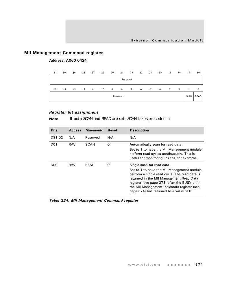
www.d i g i . com 371
E t he r n e t Commun i c a t i o n Modu l e
MII Management Command register
Address: A060 0424
Register bit assignment
Note: If both SCAN and READ are set, SCAN takes precedence.
Bits Access Mnemonic Reset Description
D31:02 N/A Reserved N/A N/A
D01 R/W SCAN 0 Automatically scan for read dataSet to 1 to have the MII Management module perform read cycles continuously. This is useful for monitoring link fail, for example.
D00 R/W READ 0 Single scan for read dataSet to 1 to have the MII Management module perform a single read cycle. The read data is returned in the MII Management Read Data register (see page 373) after the BUSY bit in the MII Management Indicators register (see page 374) has returned to a value of 0.
Table 224: MII Management Command register
Reserved
READ
13 12 11 10 9 8 7 6 5 4 3 2 1 015 14
31 29 28 27 26 25 24 23 22 21 20 19 18 17 1630
Reserved SCAN
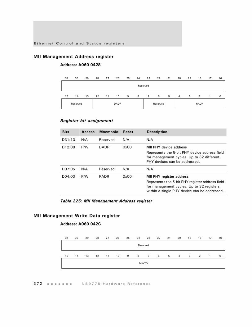
E t he r n e t Con t r o l a nd S t a t u s r eg i s t e r s
3 7 2 NS9775 Ha r dwa r e Re f e r ence
MII Management Address register
Address: A060 0428
Register bit assignment
MII Management Write Data register
Address: A060 042C
Bits Access Mnemonic Reset Description
D31:13 N/A Reserved N/A N/A
D12:08 R/W DADR 0x00 MII PHY device addressRepresents the 5-bit PHY device address field for management cycles. Up to 32 different PHY devices can be addressed.
D07:05 N/A Reserved N/A N/A
D04:00 R/W RADR 0x00 MII PHY register addressRepresents the 5-bit PHY register address field for management cycles. Up to 32 registers within a single PHY device can be addressed.
Table 225: MII Management Address register
Reserved
13 12 11 10 9 8 7 6 5 4 3 2 1 015 14
31 29 28 27 26 25 24 23 22 21 20 19 18 17 1630
DADRReserved Reserved RADR
Reserved
13 12 11 10 9 8 7 6 5 4 3 2 1 015 14
31 29 28 27 26 25 24 23 22 21 20 19 18 17 1630
MWTD
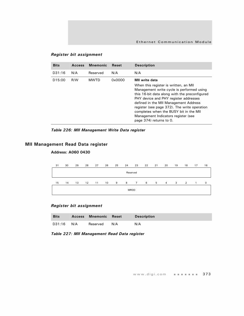
www.d i g i . com 373
E t he r n e t Commun i c a t i o n Modu l e
Register bit assignment
MII Management Read Data register
Address: A060 0430
Register bit assignment
Bits Access Mnemonic Reset Description
D31:16 N/A Reserved N/A N/A
D15:00 R/W MWTD 0x0000 MII write dataWhen this register is written, an MII Management write cycle is performed using this 16-bit data along with the preconfigured PHY device and PHY register addresses defined in the MII Management Address register (see page 372). The write operation completes when the BUSY bit in the MII Management Indicators register (see page 374) returns to 0.
Table 226: MII Management Write Data register
Bits Access Mnemonic Reset Description
D31:16 N/A Reserved N/A N/A
Table 227: MII Management Read Data register
Reserved
13 12 11 10 9 8 7 6 5 4 3 2 1 015 14
31 29 28 27 26 25 24 23 22 21 20 19 18 17 1630
MRDD
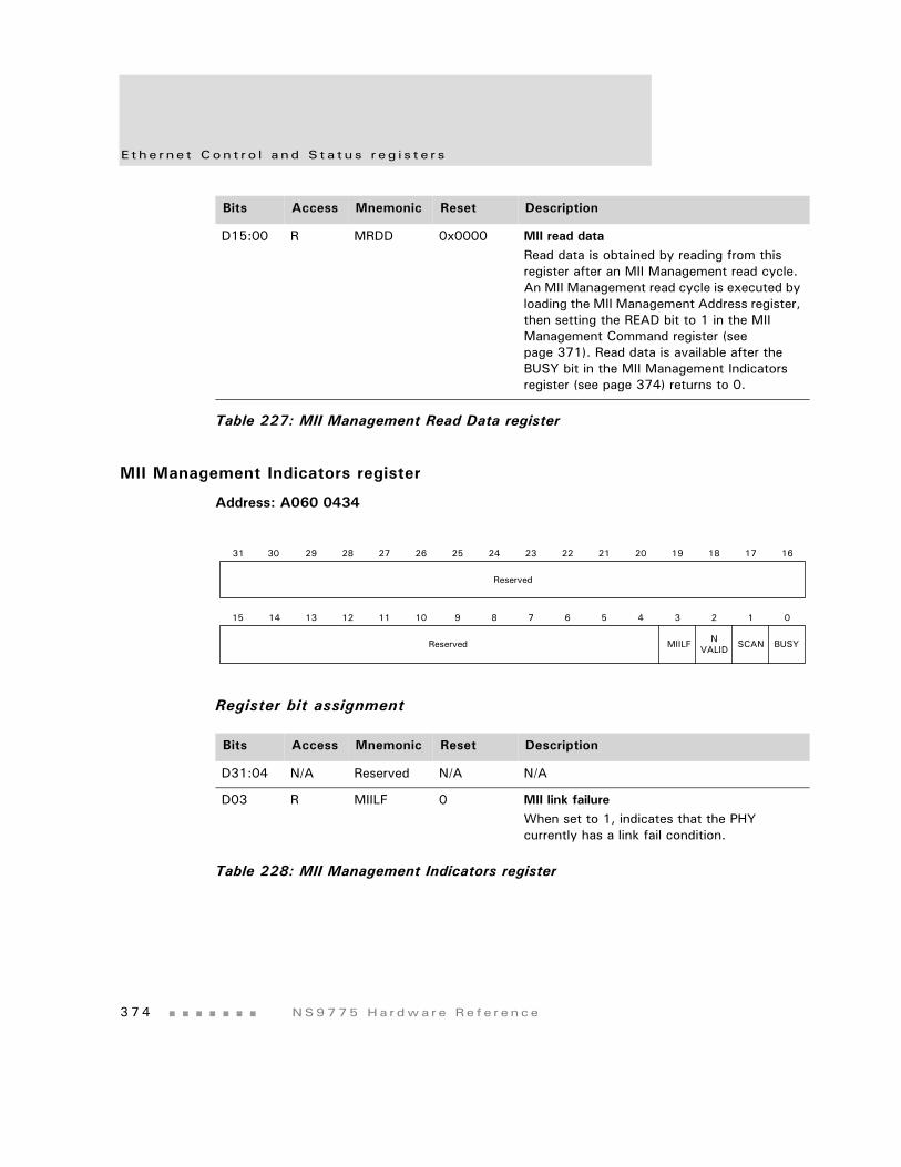
E t he r n e t Con t r o l a nd S t a t u s r eg i s t e r s
3 7 4 NS9775 Ha r dwa r e Re f e r ence
MII Management Indicators register
Address: A060 0434
Register bit assignment
D15:00 R MRDD 0x0000 MII read dataRead data is obtained by reading from this register after an MII Management read cycle. An MII Management read cycle is executed by loading the MII Management Address register, then setting the READ bit to 1 in the MII Management Command register (see page 371). Read data is available after the BUSY bit in the MII Management Indicators register (see page 374) returns to 0.
Bits Access Mnemonic Reset Description
Table 227: MII Management Read Data register
Bits Access Mnemonic Reset Description
D31:04 N/A Reserved N/A N/A
D03 R MIILF 0 MII link failureWhen set to 1, indicates that the PHY currently has a link fail condition.
Table 228: MII Management Indicators register
Reserved
MIILF BUSY
13 12 11 10 9 8 7 6 5 4 3 2 1 015 14
31 29 28 27 26 25 24 23 22 21 20 19 18 17 1630
Reserved NVALID SCAN
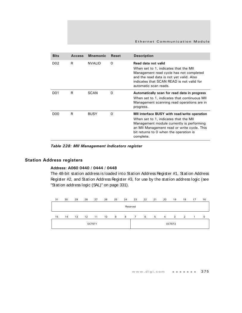
www.d i g i . com 375
E t he r n e t Commun i c a t i o n Modu l e
Station Address registers
Address: A060 0440 / 0444 / 0448The 48-bit station address is loaded into Station Address Register #1, Station Address Register #2, and Station Address Register #3, for use by the station address logic (see "Station address logic (SAL)" on page 331).
D02 R NVALID 0 Read data not validWhen set to 1, indicates that the MII Management read cycle has not completed and the read data is not yet valid. Also indicates that SCAN READ is not valid for automatic scan reads.
D01 R SCAN 0 Automatically scan for read data in progressWhen set to 1, indicates that continuous MII Management scanning read operations are in progress.
D00 R BUSY 0 MII interface BUSY with read/write operationWhen set to 1, indicates that the MII Management module currently is performing an MII Management read or write cycle. This bit returns to 0 when the operation is complete.
Bits Access Mnemonic Reset Description
Table 228: MII Management Indicators register
Reserved
OCTET1
13 12 11 10 9 8 7 6 5 4 3 2 1 015 14
31 29 28 27 26 25 24 23 22 21 20 19 18 17 1630
OCTET2
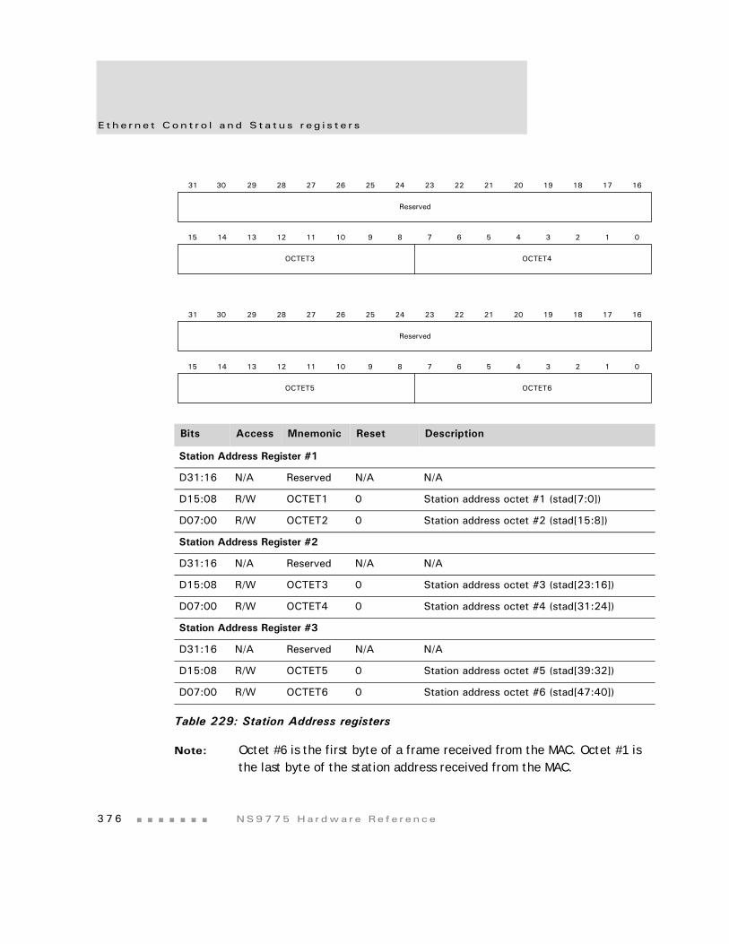
E t he r n e t Con t r o l a nd S t a t u s r eg i s t e r s
3 7 6 NS9775 Ha r dwa r e Re f e r ence
Note: Octet #6 is the first byte of a frame received from the MAC. Octet #1 is the last byte of the station address received from the MAC.
Bits Access Mnemonic Reset Description
Station Address Register #1
D31:16 N/A Reserved N/A N/A
D15:08 R/W OCTET1 0 Station address octet #1 (stad[7:0])
D07:00 R/W OCTET2 0 Station address octet #2 (stad[15:8])
Station Address Register #2
D31:16 N/A Reserved N/A N/A
D15:08 R/W OCTET3 0 Station address octet #3 (stad[23:16])
D07:00 R/W OCTET4 0 Station address octet #4 (stad[31:24])
Station Address Register #3
D31:16 N/A Reserved N/A N/A
D15:08 R/W OCTET5 0 Station address octet #5 (stad[39:32])
D07:00 R/W OCTET6 0 Station address octet #6 (stad[47:40])
Table 229: Station Address registers
Reserved
OCTET3
13 12 11 10 9 8 7 6 5 4 3 2 1 015 14
31 29 28 27 26 25 24 23 22 21 20 19 18 17 1630
OCTET4
Reserved
OCTET5
13 12 11 10 9 8 7 6 5 4 3 2 1 015 14
31 29 28 27 26 25 24 23 22 21 20 19 18 17 1630
OCTET6
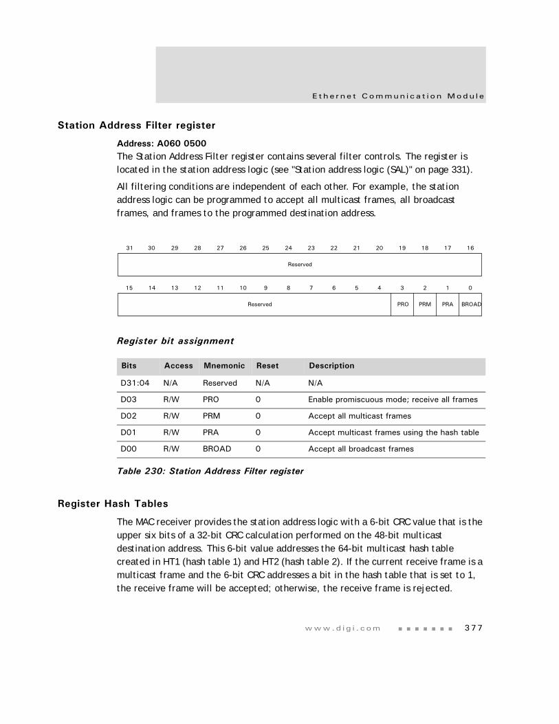
www.d i g i . com 377
E t he r n e t Commun i c a t i o n Modu l e
Station Address Filter register
Address: A060 0500The Station Address Filter register contains several filter controls. The register is located in the station address logic (see "Station address logic (SAL)" on page 331).
All filtering conditions are independent of each other. For example, the station address logic can be programmed to accept all multicast frames, all broadcast frames, and frames to the programmed destination address.
Register bit assignment
Register Hash Tables
The MAC receiver provides the station address logic with a 6-bit CRC value that is the upper six bits of a 32-bit CRC calculation performed on the 48-bit multicast destination address. This 6-bit value addresses the 64-bit multicast hash table created in HT1 (hash table 1) and HT2 (hash table 2). If the current receive frame is a multicast frame and the 6-bit CRC addresses a bit in the hash table that is set to 1, the receive frame will be accepted; otherwise, the receive frame is rejected.
Bits Access Mnemonic Reset Description
D31:04 N/A Reserved N/A N/A
D03 R/W PRO 0 Enable promiscuous mode; receive all frames
D02 R/W PRM 0 Accept all multicast frames
D01 R/W PRA 0 Accept multicast frames using the hash table
D00 R/W BROAD 0 Accept all broadcast frames
Table 230: Station Address Filter register
Reserved
PRO BROAD
13 12 11 10 9 8 7 6 5 4 3 2 1 015 14
31 29 28 27 26 25 24 23 22 21 20 19 18 17 1630
Reserved PRM PRA
E t he r n e t Con t r o l a nd S t a t u s r eg i s t e r s
3 7 8 NS9775 Ha r dwa r e Re f e r ence
HT1 stores enables for the lower 32 CRC addresses; HT2 stores enables for the upper 32 CRC addresses.
HT1
Address: A060 0504
Register bit assignment
HT2
Address: A060 0508
Register bit assignment
Bits Access Mnemonic Reset Description
D31:00 R/W HT1 0x00000000 CRC 31:00
Table 231: Hash Table Register 1
Bits Access Mnemonic Reset Description
D31:00 R/W HT2 0x00000000 CRC 63:32
Table 232: Hash Table Register 2
HT1
13 12 11 10 9 8 7 6 5 4 3 2 1 015 14
31 29 28 27 26 25 24 23 22 21 20 19 18 17 1630
HT1
HT2
13 12 11 10 9 8 7 6 5 4 3 2 1 015 14
31 29 28 27 26 25 24 23 22 21 20 19 18 17 1630
HT2
www.d i g i . com 379
E t he r n e t Commun i c a t i o n Modu l e
Statistics registers
Address: A060 0680 (base register)The Statistics module has 39 counters and 4 support registers that count and save Ethernet statistics. The Ethernet General Control Register #2 contains three Statistics module configuration bits: AUTOZ, CLRCNT, and STEN. The counters support a “clear on read” capability that is enabled when AUTOZ is set to 1.
Combined transmit and receive statistics counters
The combined transmit and receive statistics counters, listed in Table 233, are incremented for each good or bad frame, transmitted and received, that falls within the specified frame length limits of the counter (for example, TR127 counts 65–127 byte frames). The frame length excludes framing bits and includes the FCS (checksum) bytes. All counters are 18 bits, with this bit configuration:
D31:18 R Reserved
D17:00 R/W Reset = 0x00000 Count (R/W)
Address Register Transmit and receive counters R/W
A060_0680 TR64 Transmit & receive 64 Byte frame counter R/W
A060_0684 TR127 Transmit & receive 65 to 127 Byte frame counter R/W
A060_0688 TR255 Transmit & receive 128 to 255 Byte frame counter R/W
A060_068C TR511 Transmit & receive 256 to 511 Byte frame counter R/W
A060_0690 TR1K Transmit & receive 512 to 1023 Byte frame counter R/W
A060_0694 TRMAX Transmit & receive 1024 to 1518 Byte frame counter R/W
A060_0698 TRMGV Transmit & receive 1519 to 1522 Byte good VLAN frame count
R/W
Table 233: Combined transmit and receive statistics counters address map
E t he r n e t Con t r o l a nd S t a t u s r eg i s t e r s
3 8 0 NS9775 Ha r dwa r e Re f e r ence
Receive statistics counters
Receive byte counter (A060 069C)Incremented by the byte count of frames received with 0 to 1518 bytes, including those in bad packets, excluding framing bits but including FCS bytes.
Address Register Receive counters R/W
A060_069C RBYT Receive byte counter R/W
A060_06A0 RPKT Receive packet counter R/W
A060_06A4 RFCS Receive FCS error counter R/W
A060_06A8 RMCA Receive multicast packet counter R/W
A060_06AC RBCA Receive broadcast packet counter R/W
A060_06B0 RXCF Receive control frame packet counter R/W
A060_06B4 RXPF Receive PAUSE frame packet counter R/W
A060_06B8 RXUO Receive unknown OPCODE counter R/W
A060_06BC RALN Receive alignment error counter R/W
A060_06C0 Reserved N/A N/A
A060_06C4 RCDE Receive code error counter R/W
A060_06C8 RCSE Receive carrier sense error counter R/W
A060_06CC RUND Receive undersize packet counter R/W
A060_06D0 ROVR Receive oversize packet counter R/W
A060_06D4 RFRG Receive fragments counter R/W
A060_06D8 RJBR Receive jabber counter R/W
A060-06DC Reserved N/A N/A
Table 234: Receive statistics counters address map
D31:24 R Reset = Read as 0 Reserved
D23:00 R/W Reset = 0x000000 RBYT
www.d i g i . com 381
E t he r n e t Commun i c a t i o n Modu l e
Receive packet counter (A060 06A0)Incremented for each received frame (including bad packets, and all unicast, broadcast, and multicast packets).
Receive FCS error counter (A060 06A4)Incremented for each frame received with a length of 64 to 1518 bytes, and containing a frame check sequence (FCS) error. FCS errors are not counted for VLAN frames that exceed 1518 bytes or for any frames with dribble bits.
Ignore this counter for RMII applications as it does not operate properly.
Receive multicast packet counter (A060 06A8)Incremented for each good multicast frame with a length no greater than 1518 bytes (non-VLAN) or 1522 bytes (VLAN), excluding broadcast frames. This counter does not look at range/length errors.
Receive broadcast packet counter (A060 06AC)Incremented for each good broadcast frame with a length no greater than 1518 bytes (non-VLAN) or 1522 bytes (VLAN), excluding multicast frames. This counter does not look at range/length errors.
D31:18 R Reset = Read as 0 Reserved
D17:00 R/W Reset = 0x00000 RPKT
D31:12 R Reset = Read as 0 Reserved
D11:00 R/W Reset = 0x000 RFCS
D31:18 R Reset = Read as 0 Reserved
D17:00 R/W Reset = 0x00000 RMCA
D31:18 R Reset = Read as 0 Reserved
D17:00 R/W Reset = 0x00000 RBCA
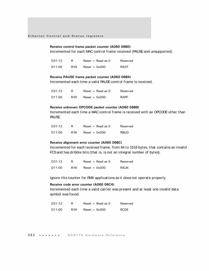
E t he r n e t Con t r o l a nd S t a t u s r eg i s t e r s
3 8 2 NS9775 Ha r dwa r e Re f e r ence
Receive control frame packet counter (A060 06B0)Incremented for each MAC control frame received (PAUSE and unsupported).
Receive PAUSE frame packet counter (A060 06B4)Incremented each time a valid PAUSE control frame is received.
Receive unknown OPCODE packet counter (A060 06B8)Incremented each time a MAC control frame is received with an OPCODE other than PAUSE.
Receive alignment error counter (A060 06BC)Incremented for each received frame, from 64 to 1518 bytes, that contains an invalid FCS and has dribble bits (that is, is not an integral number of bytes).
Ignore this counter for RMII applications as it does not operate properly.
Receive code error counter (A060 06C4)Incremented each time a valid carrier was present and at least one invalid data symbol was found.
D31:12 R Reset = Read as 0 Reserved
D11:00 R/W Reset = 0x000 RXCF
D31:12 R Reset = Read as 0 Reserved
D11:00 R/W Reset = 0x000 RXPF
D31:12 R Reset = Read as 0 Reserved
D11:00 R/W Reset = 0x000 RBUO
D31:12 R Reset = Read as 0 Reserved
D11:00 R/W Reset = 0x000 RALN
D31:12 R Reset = Read as 0 Reserved
D11:00 R/W Reset = 0x000 RCDE
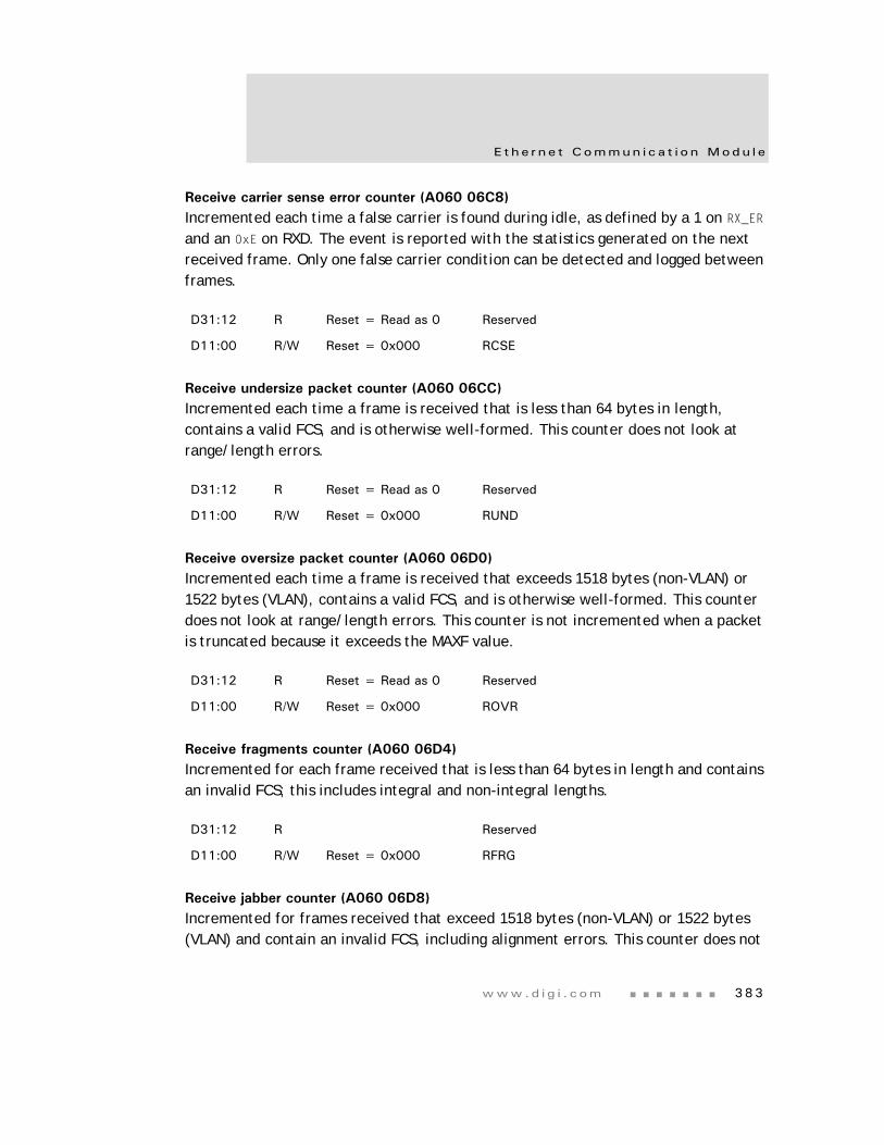
www.d i g i . com 383
E t he r n e t Commun i c a t i o n Modu l e
Receive carrier sense error counter (A060 06C8)Incremented each time a false carrier is found during idle, as defined by a 1 on RX_ER and an 0xE on RXD. The event is reported with the statistics generated on the next received frame. Only one false carrier condition can be detected and logged between frames.
Receive undersize packet counter (A060 06CC)Incremented each time a frame is received that is less than 64 bytes in length, contains a valid FCS, and is otherwise well-formed. This counter does not look at range/length errors.
Receive oversize packet counter (A060 06D0)Incremented each time a frame is received that exceeds 1518 bytes (non-VLAN) or 1522 bytes (VLAN), contains a valid FCS, and is otherwise well-formed. This counter does not look at range/length errors. This counter is not incremented when a packet is truncated because it exceeds the MAXF value.
Receive fragments counter (A060 06D4)Incremented for each frame received that is less than 64 bytes in length and contains an invalid FCS; this includes integral and non-integral lengths.
Receive jabber counter (A060 06D8)Incremented for frames received that exceed 1518 bytes (non-VLAN) or 1522 bytes (VLAN) and contain an invalid FCS, including alignment errors. This counter does not
D31:12 R Reset = Read as 0 Reserved
D11:00 R/W Reset = 0x000 RCSE
D31:12 R Reset = Read as 0 Reserved
D11:00 R/W Reset = 0x000 RUND
D31:12 R Reset = Read as 0 Reserved
D11:00 R/W Reset = 0x000 ROVR
D31:12 R Reserved
D11:00 R/W Reset = 0x000 RFRG
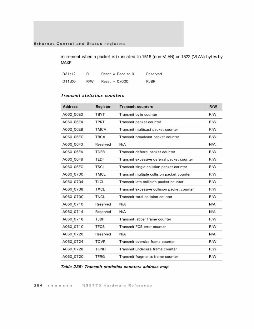
E t he r n e t Con t r o l a nd S t a t u s r eg i s t e r s
3 8 4 NS9775 Ha r dwa r e Re f e r ence
increment when a packet is truncated to 1518 (non-VLAN) or 1522 (VLAN) bytes by MAXF.
Transmit statistics counters
D31:12 R Reset = Read as 0 Reserved
D11:00 R/W Reset = 0x000 RJBR
Address Register Transmit counters R/W
A060_06E0 TBYT Transmit byte counter R/W
A060_06E4 TPKT Transmit packet counter R/W
A060_06E8 TMCA Transmit multicast packet counter R/W
A060_06EC TBCA Transmit broadcast packet counter R/W
A060_06F0 Reserved N/A N/A
A060_06F4 TDFR Transmit deferral packet counter R/W
A060_06F8 TEDF Transmit excessive deferral packet counter R/W
A060_06FC TSCL Transmit single collision packet counter R/W
A060_0700 TMCL Transmit multiple collision packet counter R/W
A060_0704 TLCL Transmit late collision packet counter R/W
A060_0708 TXCL Transmit excessive collision packet counter R/W
A060_070C TNCL Transmit total collision counter R/W
A060_0710 Reserved N/A N/A
A060_0714 Reserved N/A N/A
A060_0718 TJBR Transmit jabber frame counter R/W
A060_071C TFCS Transmit FCS error counter R/W
A060_0720 Reserved N/A N/A
A060_0724 TOVR Transmit oversize frame counter R/W
A060_0728 TUND Transmit undersize frame counter R/W
A060_072C TFRG Transmit fragments frame counter R/W
Table 235: Transmit statistics counters address map
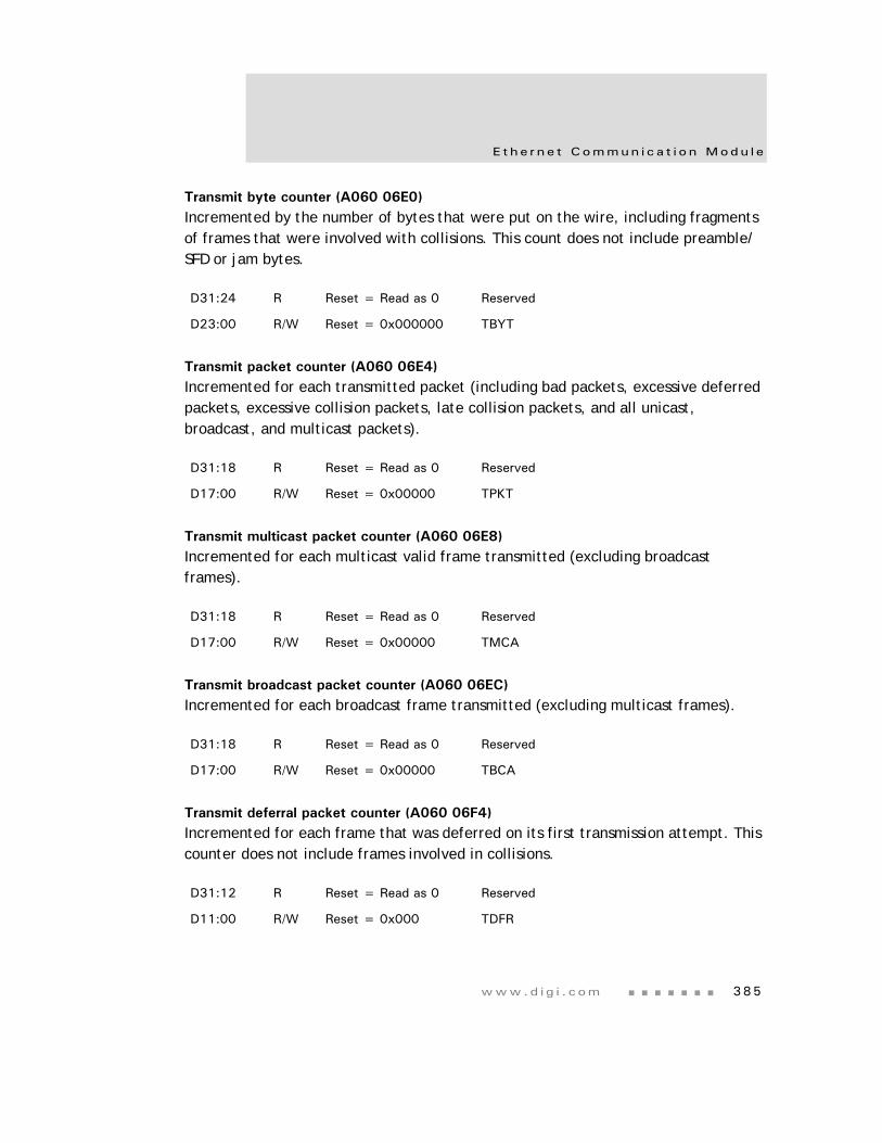
www.d i g i . com 385
E t he r n e t Commun i c a t i o n Modu l e
Transmit byte counter (A060 06E0)Incremented by the number of bytes that were put on the wire, including fragments of frames that were involved with collisions. This count does not include preamble/SFD or jam bytes.
Transmit packet counter (A060 06E4)Incremented for each transmitted packet (including bad packets, excessive deferred packets, excessive collision packets, late collision packets, and all unicast, broadcast, and multicast packets).
Transmit multicast packet counter (A060 06E8)Incremented for each multicast valid frame transmitted (excluding broadcast frames).
Transmit broadcast packet counter (A060 06EC)Incremented for each broadcast frame transmitted (excluding multicast frames).
Transmit deferral packet counter (A060 06F4)Incremented for each frame that was deferred on its first transmission attempt. This counter does not include frames involved in collisions.
D31:24 R Reset = Read as 0 Reserved
D23:00 R/W Reset = 0x000000 TBYT
D31:18 R Reset = Read as 0 Reserved
D17:00 R/W Reset = 0x00000 TPKT
D31:18 R Reset = Read as 0 Reserved
D17:00 R/W Reset = 0x00000 TMCA
D31:18 R Reset = Read as 0 Reserved
D17:00 R/W Reset = 0x00000 TBCA
D31:12 R Reset = Read as 0 Reserved
D11:00 R/W Reset = 0x000 TDFR
E t he r n e t Con t r o l a nd S t a t u s r eg i s t e r s
3 8 6 NS9775 Ha r dwa r e Re f e r ence
Transmit excessive deferral packet counter (A060 06F8)Incremented for frames aborted because they were deferred for an excessive period of time (3036 byte times).
Transmit single collision packet counter (A060 06FC)Incremented for each frame transmitted that experienced exactly one collision during transmission.
Transmit multiple collision packet counter (A060 0700)Incremented for each frame transmitted that experienced 2–15 collisions (including any late collisions) during transmission.
Transmit late collision packet counter (A060 0704)Incremented for each frame transmitted that experienced a late collision during a transmission attempt. Late collisions are defined using the CWIN[13:08] field of the Collision Window/Retry register.
Transmit excessive collision packet counter (A060 0708)Incremented for each frame transmitted that experienced excessive collisions during transmission, as defined by the RETX [03:00] field of the Collision Window/Retry register, and was aborted.
D31:12 R Reset = Read as 0 Reserved
D11:00 R/W Reset = 0x000 TEDF
D31:12 R Reset = Read as 0 Reserved
D11:00 R/W Reset = 0x000 TSCL
D31:12 R Reset = Read as 0 Reserved
D11:00 R/W Reset = 0x000 TMCL
D31:12 R Reset = Read as 0 Reserved
D11:00 R/W Reset = 0x000 TLCL
D31:12 R Reset = Read as 0 Reserved
D11:00 R/W Reset = 0x000 TXCL
www.d i g i . com 387
E t he r n e t Commun i c a t i o n Modu l e
Transmit total collision packet counter (A060 070C)Incremented by the number of collisions experienced during the transmission of a frame.
Note: This register does not include collisions that result in an excessive collision count or late collisions.
Transmit jabber frame counter (A060 0718)Incremented for each oversized transmitted frame with an incorrect FCS value.
Transmit FCS error counter (A060 071C)Incremented for every valid-sized packet with an incorrect FCS value.
Transmit oversize frame counter (A060 0724)Incremented for each transmitted frame that exceeds 1518 bytes (NON_VLAN) or 1522 bytes (VLAN) and contains a valid FCS.
D31:12 R Reset = Read as 0 Reserved
D11:00 R/W Reset = 0x000 TNCL
D31:12 R Reset = Read as 0 Reserved
D11:00 R/W Reset = 0x000 TJBR
D31:12 R Reset = Read as 0 Reserved
D11:00 R/W Reset = 0x000 TFCS
D31:12 R Reset = Read as 0 Reserved
D11:00 R/W Reset = 0x000 TOVR
E t he r n e t Con t r o l a nd S t a t u s r eg i s t e r s
3 8 8 NS9775 Ha r dwa r e Re f e r ence
Transmit undersize frame counter (A060 0728)Incremented for every frame less than 64 bytes, with a correct FCS value. This counter also is incremented when a jumbo packet is aborted (see "TXAJ" on page 356) and the MAC is not checking the FCS (see "CRCEN" on page 363), because the frame is reported as having a length of 0 bytes.
Transmit fragment counter (A060 072C)Incremented for every frame less than 64 bytes, with an incorrect FCS value.
General Statistics registers
Table 236 lists the General Statistics registers.
Carry Register 1 (CAR1) and Carry Register 2 (CAR2) have carry bits for all of the statistics counters. These carry bits are set when the associated counter reaches a rollover condition.
These carry bits also can cause the STOVFL (statistics counter overflow) bit in the Ethernet Interrupt Status register (see "Ethernet Interrupt Status register" on page 396) to be set. Carry Register 1 Mask register (CAM1) and Carry Register 2 Mask register (CAM2) have individual mask bits for each of the carry bits. When set, the mask bit prevents the associated carry bit from setting the STOVFL bit.
D31:12 R Reset = Read as 0 Reserved
D11:00 R/W Reset = 0x000 TUND
D31:12 R Reset = Read as 0 Reserved
D11:00 R/W Reset = 0x000 TFRG
Address Register General registers R/W
A060_0730 CAR1 Carry Register 1 R
A060_0734 CAR2 Carry Register 2 R
A060_0738 CAM1 Carry Register 1 Mask register R/W
A060_073C CAM2 Carry Register 2 Mask register R/W
Table 236: General Statistics register address map
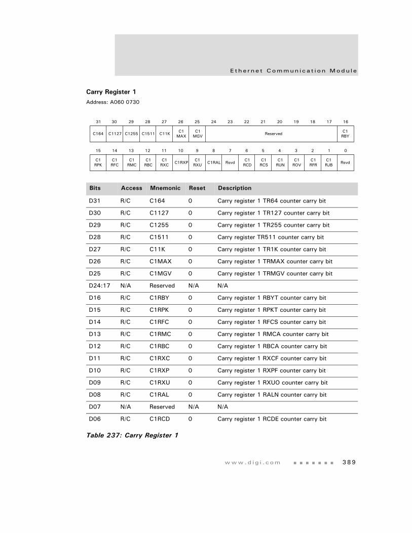
www.d i g i . com 389
E t he r n e t Commun i c a t i o n Modu l e
Carry Register 1Address: A060 0730
Bits Access Mnemonic Reset Description
D31 R/C C164 0 Carry register 1 TR64 counter carry bit
D30 R/C C1127 0 Carry register 1 TR127 counter carry bit
D29 R/C C1255 0 Carry register 1 TR255 counter carry bit
D28 R/C C1511 0 Carry register TR511 counter carry bit
D27 R/C C11K 0 Carry register 1 TR1K counter carry bit
D26 R/C C1MAX 0 Carry register 1 TRMAX counter carry bit
D25 R/C C1MGV 0 Carry register 1 TRMGV counter carry bit
D24:17 N/A Reserved N/A N/A
D16 R/C C1RBY 0 Carry register 1 RBYT counter carry bit
D15 R/C C1RPK 0 Carry register 1 RPKT counter carry bit
D14 R/C C1RFC 0 Carry register 1 RFCS counter carry bit
D13 R/C C1RMC 0 Carry register 1 RMCA counter carry bit
D12 R/C C1RBC 0 Carry register 1 RBCA counter carry bit
D11 R/C C1RXC 0 Carry register 1 RXCF counter carry bit
D10 R/C C1RXP 0 Carry register 1 RXPF counter carry bit
D09 R/C C1RXU 0 Carry register 1 RXUO counter carry bit
D08 R/C C1RAL 0 Carry register 1 RALN counter carry bit
D07 N/A Reserved N/A N/A
D06 R/C C1RCD 0 Carry register 1 RCDE counter carry bit
Table 237: Carry Register 1
C1RMC
C1RBC C1RXPC1
RXCC1
RXU C1RAL C1RCD
C1RCS
C1RUN
C1ROV
C1RFR
C1RJB Rsvd
13 12 11 10 9 8 7 6 5 4 3 2 1 015 14
C1RPK
C1RFC
31 29 28 27 26 25 24 23 22 21 20 19 18 17 1630
C1255 C1511 C1MAXC11K C1
MGVC1RBYC164 C1127 Reserved
Rsvd
E t he r n e t Con t r o l a nd S t a t u s r eg i s t e r s
3 9 0 NS9775 Ha r dwa r e Re f e r ence
Carry Register 2Address: A060 0734
D05 R/C C1RCS 0 Carry register 1 RCSE counter carry bit
D04 R/C C1RUN 0 Carry register 1 RUND counter carry register
D03 R/C C1ROV 0 Carry register 1 ROVR counter carry bit
D02 R/C C1RFR 0 Carry register 1 RFRG counter carry bit
D01 R/C C1RJB 0 Carry register 1 RJBR counter carry bit
D00 N/A Reserved N/A N/A
Bits Access Mnemonic Reset Description
D31:20 N/A Reserved N/A N/A
D19 R/C C2TJB 0 Carry register 2 TJBR counter carry bit
D18 R/C C2TFC 0 Carry register 2 TFCS counter carry bit
D17 N/A Reserved N/A N/A
D16 R/C C2TOV 0 Carry register 2 TOVR counter carry bit
D15 R/C C2TUN 0 Carry register 2 TUND counter carry bit
D14 R/C C2TFG 0 Carry register 2 TFRG counter carry bit
D13 R/C C2TBY 0 Carry register 2 TBYT counter carry bit
D12 R/C C2TPK 0 Carry register 2 TPKT counter carry bit
D11 R/C C2TMC 0 Carry register 2 TMCA counter carry bit
Table 238: Carry Register 2
Bits Access Mnemonic Reset Description
Table 237: Carry Register 1
C2TBY
C2TPK C2TBCC2TMC Rsvd C2TDF C2
TEDC2
TSCC2
TMAC2TLC
C2TXC
C2TNC Reserved
13 12 11 10 9 8 7 6 5 4 3 2 1 015 14
C2TUN
C2TFG
31 29 28 27 26 25 24 23 22 21 20 19 18 17 1630
Reserved C2JTB
C2TFC Rsvd C2
TOV
www.d i g i . com 391
E t he r n e t Commun i c a t i o n Modu l e
Carry Register 1 Mask registerAddress: A060 0738
D10 R/C C2TBC 0 Carry register 2 TBCA counter carry bit
D09 N/A Reserved N/A N/A
D08 R/C C2TDF 0 Carry register 2TDFR counter carry bit
D07 R/C C2TED 0 Carry register 2 TEDF counter carry bit
D06 R/C C2TSC 0 Carry register 2 TSCL counter carry bit
D05 R/C C2TMA 0 Carry register 2 TMCL counter carry bit
D04 R/C C2TLC 0 Carry register 2 TLCL counter carry bit
D03 R/C C2TXC 0 Carry register 2 TXCL counter carry bit
D02 R/C C2TNC 0 Carry register 2 TNCL counter carry bit
D01:00 N/A Reserved N/A N/A
Bits Access Mnemonic Reset Description
D31 R/W M164 1 Mask register 1 TR64 counter carry bit mask
D30 R/W M1127 1 Mask register 1 TR127 counter carry bit mask
D29 R/W M1255 1 Mask register 1 TR255 counter carry bit mask
D28 R/W M1511 1 Mask register 1 TR511 counter carry bit mask
D27 R/W M11K 1 Mask register 1 TR1K counter carry bit mask
D26 R/W M1MAX 1 Mask register 1 TRMAX counter carry bit mask
Table 239: Carry Register 1 Mask register
Bits Access Mnemonic Reset Description
Table 238: Carry Register 2
M1RMC
M1RBC M1RXPM1
RXCM1RXU M1RAL M1
RCDM1RCS
M1RUN
M1ROV
M1RFR
M1RJB
Notused
13 12 11 10 9 8 7 6 5 4 3 2 1 015 14
M1RPK
M1RFC
31 29 28 27 26 25 24 23 22 21 20 19 18 17 1630
M1255
M1511
M1MAX
MC11K
M1MGV
M1RBYM164 M1127 Reserved
Notused
E t he r n e t Con t r o l a nd S t a t u s r eg i s t e r s
3 9 2 NS9775 Ha r dwa r e Re f e r ence
D25 R/W M1MGV 1 Mask register 1 TRMGV counter carry bit mask
D24:17 N/A Reserved N/A N/A
D16 R/W M1RBY 1 Mask register 1 RBYT counter carry bit mask
D15 R/W M1RPK 1 Mask register 1 RPKT counter carry bit mask
D14 R/W M1RFC 1 Mask register 1 RFCS counter carry bit mask. Set this bit to 1 for RMII applications.
D13 R/W M1RMC 1 Mask register 1 RMCA counter carry bit mask
D12 R/W M1RBC 1 Mask register 1 RBCA counter carry bit mask
D11 R/W M1RXC 1 Mask register 1 RXCF counter carry bit mask
D10 R/W M1RXP 1 Mask register 1 RXPF counter carry bit mask
D09 R/W M1RXU 1 Mask register 1 RXUO counter carry bit mask
D08 R/W M1RAL 1 Mask register 1 RALN counter carry bit mask. Set this bit to 1 for RMII applications.
D07 N/A Not used 1 Always write as 1.
D06 R/W M1RCD 1 Mask register 1 RCDE counter carry bit mask
D05 R/W M1RCS 1 Mask register 1 RCSE counter carry bit mask
D04 R/W M1RUN 1 Mask register 1 RUND counter carry bit mask
D03 R/W M1ROV 1 Mask register 1 ROVR counter carry bit mask
D02 R/W M1RFR 1 Mask register 1 RFRG counter carry bit mask
D01 R/W M1RJB 1 Mask register 1 RJBR counter carry bit mask
D00 R/W Not used 1 Always write as 1.
Bits Access Mnemonic Reset Description
Table 239: Carry Register 1 Mask register
www.d i g i . com 393
E t he r n e t Commun i c a t i o n Modu l e
Carry Register 2 Mask registerAddress: A060 073C
Bits Access Mnemonic Reset Description
D31:20 N/A Reserved N/A N/A
D19 R/W M2TJB 1 Mask register 2 TJBR counter carry bit mask
D18 R/W M2TFC 1 Mask register 2 TFCS counter carry bit mask
D17 R/W Not used 1 Always write as 1.
D16 R/W M2TOV 1 Mask register 2 TOVR counter carry bit mask
D15 R/W M2TUN 1 Mask register 2 TUND counter carry bit mask
D14 R/W M2TFG 1 Mask register 2 TFRG counter carry bit mask
D13 R/W M2TBY 1 Mask register 2 TBYT counter carry bit mask
D12 R/W M2TPK 1 Mask register 2 TPKT counter carry bit mask
D11 R/W M2TMC 1 Mask register 2 TMCA counter carry bit mask
D10 R/W M2TBC 1 Mask register 2 TBCA counter carry bit mask
D09 R/W Not used 1 Always write as 1.
D08 R/W M2TDF 1 Mask register 2 TDFR counter carry bit mask
D07 R/W M2TED 1 Mask register 2 TEDF counter carry bit mask
D06 R/W M2TSC 1 Mask register 2 TSCL counter carry bit mask
D05 R/W M2TMA 1 Mask register 2 TMCL counter carry bit mask
D04 R/W M2TLC 1 Mask register 2 TLCL counter carry bit mask
D03 R/W M2TXC 1 Mask register 2 TXCL counter carry bit mask
D02 R/W M2TNC 1 Mask register 2 TNCL counter carry bit mask
D01:00 R/W Not used 11 Always write as “11.”
Table 240: Carry Register 2 Mask register
M2TBY
M2TPK M2TBCM2
TMCNotused M2TDF M2
TEDM2TSC
M2TMA
M2TLC
M2TXC
M2TNC Not used
13 12 11 10 9 8 7 6 5 4 3 2 1 015 14
M2TUN
M2TFG
31 29 28 27 26 25 24 23 22 21 20 19 18 17 1630
Reserved M2JTB
M2TFC
Notused
M2TOV
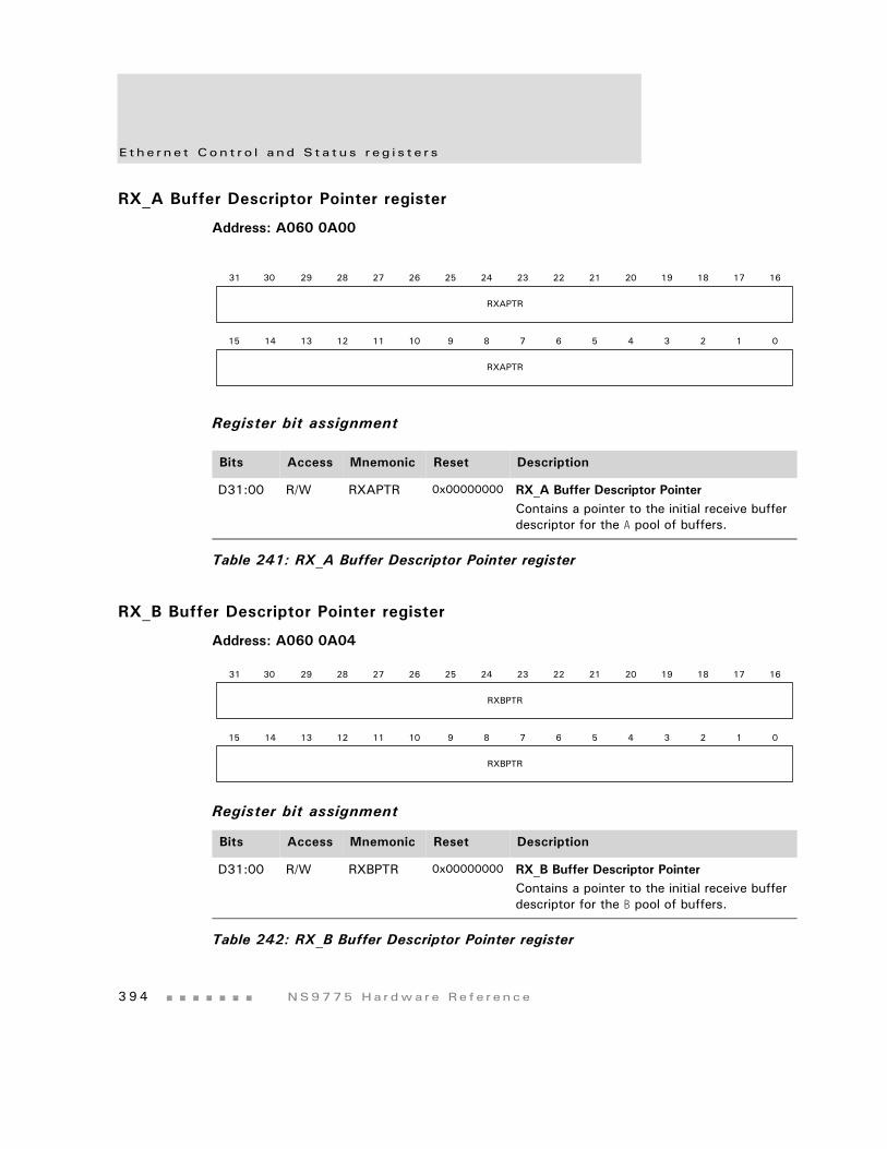
E t he r n e t Con t r o l a nd S t a t u s r eg i s t e r s
3 9 4 NS9775 Ha r dwa r e Re f e r ence
RX_A Buffer Descriptor Pointer register
Address: A060 0A00
Register bit assignment
RX_B Buffer Descriptor Pointer register
Address: A060 0A04
Register bit assignment
Bits Access Mnemonic Reset Description
D31:00 R/W RXAPTR 0x00000000 RX_A Buffer Descriptor PointerContains a pointer to the initial receive buffer descriptor for the A pool of buffers.
Table 241: RX_A Buffer Descriptor Pointer register
RXAPTR
13 12 11 10 9 8 7 6 5 4 3 2 1 015 14
31 29 28 27 26 25 24 23 22 21 20 19 18 17 1630
RXAPTR
Bits Access Mnemonic Reset Description
D31:00 R/W RXBPTR 0x00000000 RX_B Buffer Descriptor PointerContains a pointer to the initial receive buffer descriptor for the B pool of buffers.
Table 242: RX_B Buffer Descriptor Pointer register
RXBPTR
13 12 11 10 9 8 7 6 5 4 3 2 1 015 14
31 29 28 27 26 25 24 23 22 21 20 19 18 17 1630
RXBPTR
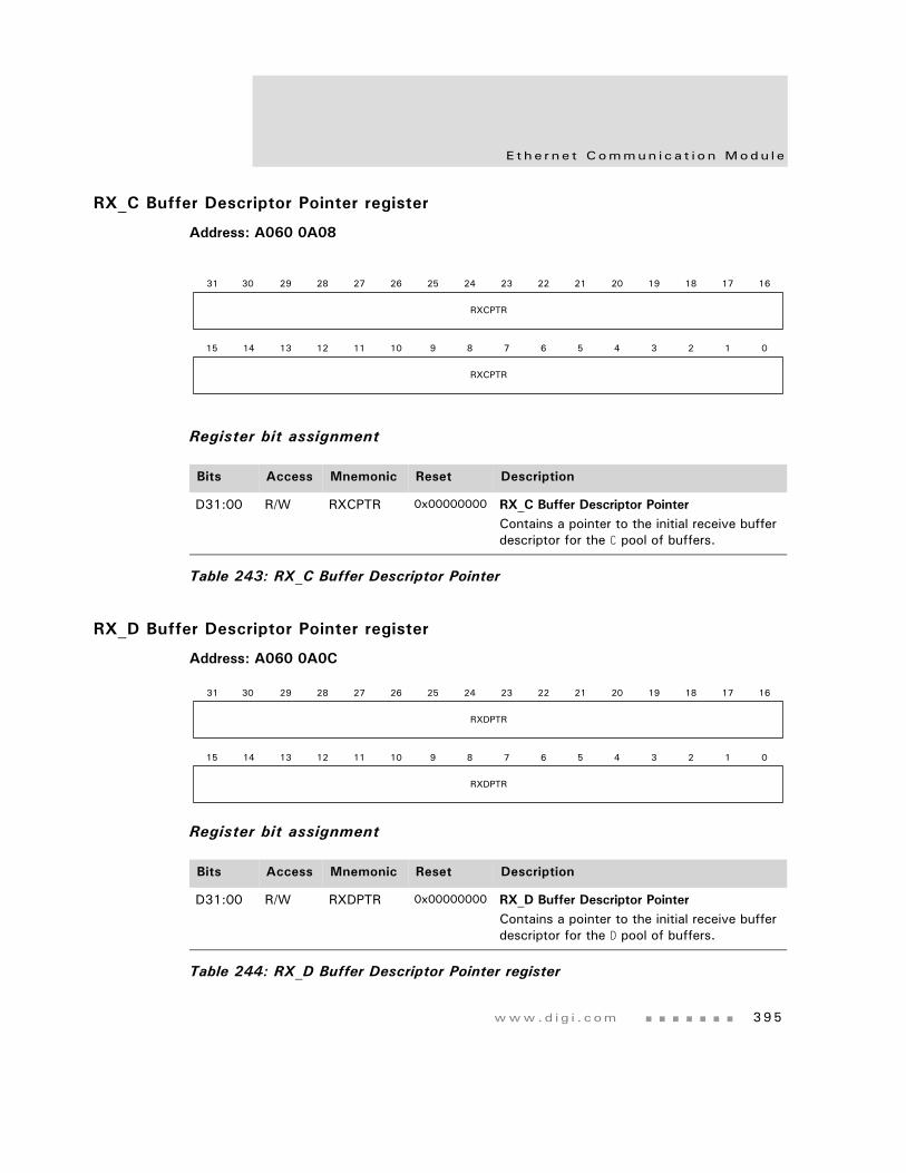
www.d i g i . com 395
E t he r n e t Commun i c a t i o n Modu l e
RX_C Buffer Descriptor Pointer register
Address: A060 0A08
Register bit assignment
RX_D Buffer Descriptor Pointer register
Address: A060 0A0C
Register bit assignment
Bits Access Mnemonic Reset Description
D31:00 R/W RXCPTR 0x00000000 RX_C Buffer Descriptor Pointer Contains a pointer to the initial receive buffer descriptor for the C pool of buffers.
Table 243: RX_C Buffer Descriptor Pointer
RXCPTR
13 12 11 10 9 8 7 6 5 4 3 2 1 015 14
31 29 28 27 26 25 24 23 22 21 20 19 18 17 1630
RXCPTR
Bits Access Mnemonic Reset Description
D31:00 R/W RXDPTR 0x00000000 RX_D Buffer Descriptor PointerContains a pointer to the initial receive buffer descriptor for the D pool of buffers.
Table 244: RX_D Buffer Descriptor Pointer register
RXDPTR
13 12 11 10 9 8 7 6 5 4 3 2 1 015 14
31 29 28 27 26 25 24 23 22 21 20 19 18 17 1630
RXDPTR
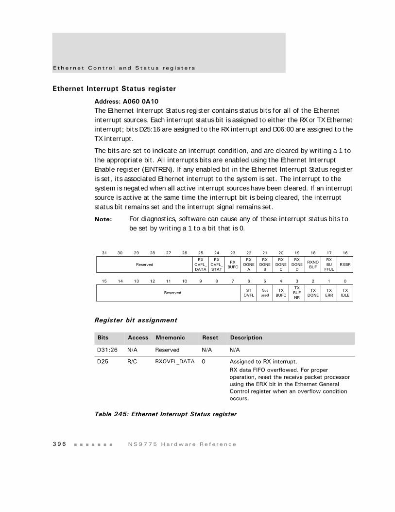
E t he r n e t Con t r o l a nd S t a t u s r eg i s t e r s
3 9 6 NS9775 Ha r dwa r e Re f e r ence
Ethernet Interrupt Status register
Address: A060 0A10The Ethernet Interrupt Status register contains status bits for all of the Ethernet interrupt sources. Each interrupt status bit is assigned to either the RX or TX Ethernet interrupt; bits D25:16 are assigned to the RX interrupt and D06:00 are assigned to the TX interrupt.
The bits are set to indicate an interrupt condition, and are cleared by writing a 1 to the appropriate bit. All interrupts bits are enabled using the Ethernet Interrupt Enable register (EINTREN). If any enabled bit in the Ethernet Interrupt Status register is set, its associated Ethernet interrupt to the system is set. The interrupt to the system is negated when all active interrupt sources have been cleared. If an interrupt source is active at the same time the interrupt bit is being cleared, the interrupt status bit remains set and the interrupt signal remains set.
Note: For diagnostics, software can cause any of these interrupt status bits to be set by writing a 1 to a bit that is 0.
Register bit assignment
Bits Access Mnemonic Reset Description
D31:26 N/A Reserved N/A N/A
D25 R/C RXOVFL_DATA 0 Assigned to RX interrupt.RX data FIFO overflowed. For proper operation, reset the receive packet processor using the ERX bit in the Ethernet General Control register when an overflow condition occurs.
Table 245: Ethernet Interrupt Status register
Reserved
13 12 11 10 9 8 7 6 5 4 3 2 1 015 14
31 29 28 27 26 25 24 23 22 21 20 19 18 17 1630
Reserved
RXDONE
C
RXDONE
D
RXNOBUF
RXBU
FFULRXBR
RXOVFL_DATA
RXOVFL_STAT
RXBUFC
RXDONE
A
RXDONE
B
STOVFL
Notused
TXBUFC
TXBUFNR
TXDONE
TXERR
TXIDLE
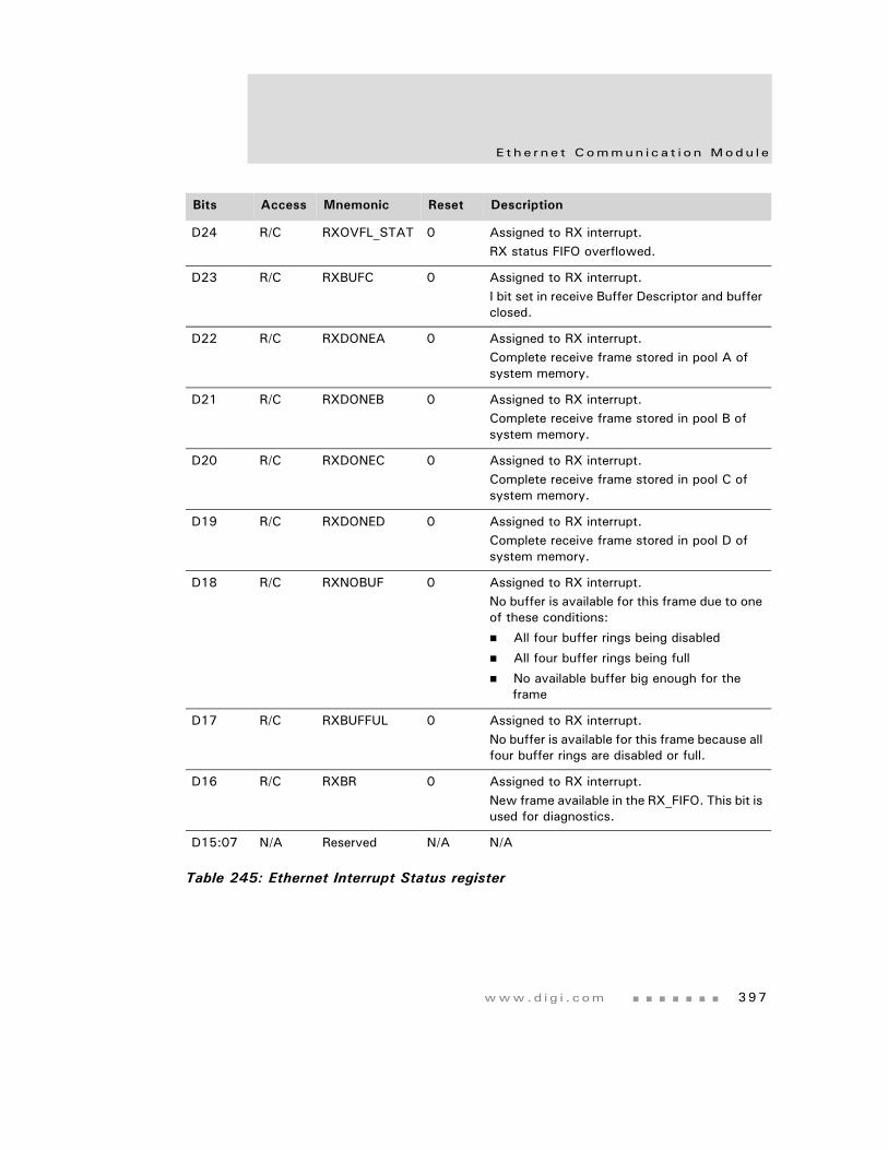
www.d i g i . com 397
E t he r n e t Commun i c a t i o n Modu l e
D24 R/C RXOVFL_STAT 0 Assigned to RX interrupt.RX status FIFO overflowed.
D23 R/C RXBUFC 0 Assigned to RX interrupt.I bit set in receive Buffer Descriptor and buffer closed.
D22 R/C RXDONEA 0 Assigned to RX interrupt.Complete receive frame stored in pool A of system memory.
D21 R/C RXDONEB 0 Assigned to RX interrupt.Complete receive frame stored in pool B of system memory.
D20 R/C RXDONEC 0 Assigned to RX interrupt.Complete receive frame stored in pool C of system memory.
D19 R/C RXDONED 0 Assigned to RX interrupt.Complete receive frame stored in pool D of system memory.
D18 R/C RXNOBUF 0 Assigned to RX interrupt.No buffer is available for this frame due to one of these conditions:
All four buffer rings being disabled
All four buffer rings being full
No available buffer big enough for the frame
D17 R/C RXBUFFUL 0 Assigned to RX interrupt.No buffer is available for this frame because all four buffer rings are disabled or full.
D16 R/C RXBR 0 Assigned to RX interrupt.New frame available in the RX_FIFO. This bit is used for diagnostics.
D15:07 N/A Reserved N/A N/A
Bits Access Mnemonic Reset Description
Table 245: Ethernet Interrupt Status register
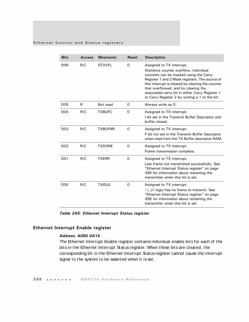
E t he r n e t Con t r o l a nd S t a t u s r eg i s t e r s
3 9 8 NS9775 Ha r dwa r e Re f e r ence
Ethernet Interrupt Enable register
Address: A060 0A14The Ethernet Interrupt Enable register contains individual enable bits for each of the bits in the Ethernet Interrupt Status register. When these bits are cleared, the corresponding bit in the Ethernet Interrupt Status register cannot cause the interrupt signal to the system to be asserted when it is set.
D06 R/C STOVFL 0 Assigned to TX interrupt.Statistics counter overflow. Individual counters can be masked using the Carry Register 1 and 2 Mask registers. The source of this interrupt is cleared by clearing the counter that overflowed, and by clearing the associated carry bit in either Carry Register 1 or Carry Register 2 by writing a 1 to the bit.
D05 R Not used 0 Always write as 0.
D04 R/C TXBUFC 0 Assigned to TX interrupt.I bit set in the Transmit Buffer Descriptor and buffer closed.
D03 R/C TXBUFNR 0 Assigned to TX interrupt.F bit not set in the Transmit Buffer Descriptor when read from the TX Buffer descriptor RAM.
D02 R/C TXDONE 0 Assigned to TX interrupt.Frame transmission complete.
D01 R/C TXERR 0 Assigned to TX interrupt.Last frame not transmitted successfully. See "Ethernet Interrupt Status register" on page 396 for information about restarting the transmitter when this bit is set.
D00 R/C TXIDLE 0 Assigned to TX interrupt.TX_WR logic has no frame to transmit. See "Ethernet Interrupt Status register" on page 396 for information about restarting the transmitter when this bit is set.
Bits Access Mnemonic Reset Description
Table 245: Ethernet Interrupt Status register
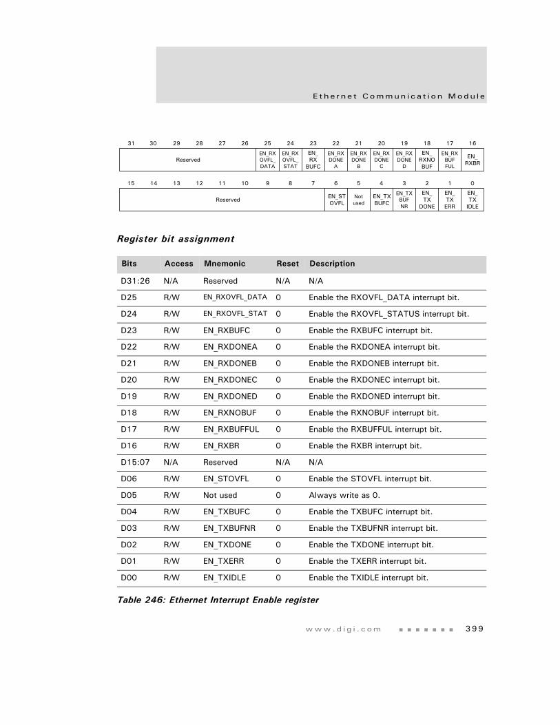
www.d i g i . com 399
E t he r n e t Commun i c a t i o n Modu l e
Register bit assignment
Bits Access Mnemonic Reset Description
D31:26 N/A Reserved N/A N/A
D25 R/W EN_RXOVFL_DATA 0 Enable the RXOVFL_DATA interrupt bit.
D24 R/W EN_RXOVFL_STAT 0 Enable the RXOVFL_STATUS interrupt bit.
D23 R/W EN_RXBUFC 0 Enable the RXBUFC interrupt bit.
D22 R/W EN_RXDONEA 0 Enable the RXDONEA interrupt bit.
D21 R/W EN_RXDONEB 0 Enable the RXDONEB interrupt bit.
D20 R/W EN_RXDONEC 0 Enable the RXDONEC interrupt bit.
D19 R/W EN_RXDONED 0 Enable the RXDONED interrupt bit.
D18 R/W EN_RXNOBUF 0 Enable the RXNOBUF interrupt bit.
D17 R/W EN_RXBUFFUL 0 Enable the RXBUFFUL interrupt bit.
D16 R/W EN_RXBR 0 Enable the RXBR interrupt bit.
D15:07 N/A Reserved N/A N/A
D06 R/W EN_STOVFL 0 Enable the STOVFL interrupt bit.
D05 R/W Not used 0 Always write as 0.
D04 R/W EN_TXBUFC 0 Enable the TXBUFC interrupt bit.
D03 R/W EN_TXBUFNR 0 Enable the TXBUFNR interrupt bit.
D02 R/W EN_TXDONE 0 Enable the TXDONE interrupt bit.
D01 R/W EN_TXERR 0 Enable the TXERR interrupt bit.
D00 R/W EN_TXIDLE 0 Enable the TXIDLE interrupt bit.
Table 246: Ethernet Interrupt Enable register
Reserved
13 12 11 10 9 8 7 6 5 4 3 2 1 015 14
31 29 28 27 26 25 24 23 22 21 20 19 18 17 1630
Reserved
EN_RXDONE
C
EN_RXDONE
D
EN_RXNOBUF
EN_RXBUFFUL
EN_RXBR
EN_RXOVFL_DATA
EN_RXOVFL_STAT
EN_RX
BUFC
EN_RXDONE
A
EN_RXDONE
B
EN_STOVFL
Notused
EN_TXBUFC
EN_TXBUFNR
EN_TX
DONE
EN_TXERR
EN_TX
IDLE
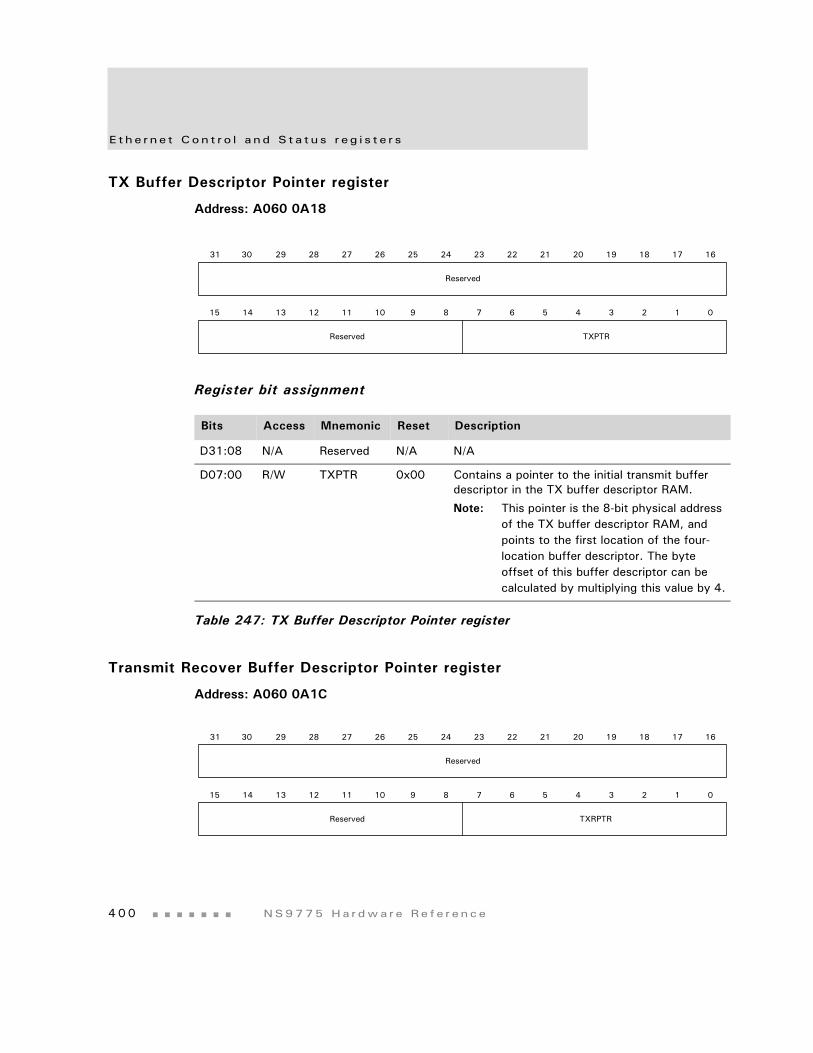
E t he r n e t Con t r o l a nd S t a t u s r eg i s t e r s
4 0 0 NS9775 Ha r dwa r e Re f e r ence
TX Buffer Descriptor Pointer register
Address: A060 0A18
Register bit assignment
Transmit Recover Buffer Descriptor Pointer register
Address: A060 0A1C
Bits Access Mnemonic Reset Description
D31:08 N/A Reserved N/A N/A
D07:00 R/W TXPTR 0x00 Contains a pointer to the initial transmit buffer descriptor in the TX buffer descriptor RAM.
Note: This pointer is the 8-bit physical address of the TX buffer descriptor RAM, and points to the first location of the four-location buffer descriptor. The byte offset of this buffer descriptor can be calculated by multiplying this value by 4.
Table 247: TX Buffer Descriptor Pointer register
Reserved
TXPTR
13 12 11 10 9 8 7 6 5 4 3 2 1 015 14
31 29 28 27 26 25 24 23 22 21 20 19 18 17 1630
Reserved
Reserved
TXRPTR
13 12 11 10 9 8 7 6 5 4 3 2 1 015 14
31 29 28 27 26 25 24 23 22 21 20 19 18 17 1630
Reserved
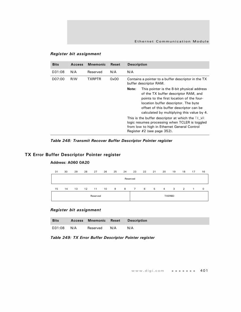
www.d i g i . com 401
E t he r n e t Commun i c a t i o n Modu l e
Register bit assignment
TX Error Buffer Descriptor Pointer register
Address: A060 0A20
Register bit assignment
Bits Access Mnemonic Reset Description
D31:08 N/A Reserved N/A N/A
D07:00 R/W TXRPTR 0x00 Contains a pointer to a buffer descriptor in the TX buffer descriptor RAM.
Note: This pointer is the 8-bit physical address of the TX buffer descriptor RAM, and points to the first location of the four-location buffer descriptor. The byte offset of this buffer descriptor can be calculated by multiplying this value by 4.
This is the buffer descriptor at which the TX_WR logic resumes processing when TCLER is toggled from low to high in Ethernet General Control Register #2 (see page 352).
Table 248: Transmit Recover Buffer Descriptor Pointer register
Bits Access Mnemonic Reset Description
D31:08 N/A Reserved N/A N/A
Table 249: TX Error Buffer Descriptor Pointer register
Reserved
TXERBD
13 12 11 10 9 8 7 6 5 4 3 2 1 015 14
31 29 28 27 26 25 24 23 22 21 20 19 18 17 1630
Reserved
E t he r n e t Con t r o l a nd S t a t u s r eg i s t e r s
4 0 2 NS9775 Ha r dwa r e Re f e r ence
TX Stall Buffer Descriptor Pointer register
Address: A060 0A24
Register bit assignment
D07:00 R TXERBD 0x00 Contains the pointer (in the TX buffer descriptor RAM) to the last buffer descriptor of a frame that was not successfully transmitted. TXERBD is loaded by the TX_WR logic when a transmit frame is aborted by the MAC or when the MAC finds a CRC error in a frame. TXERBD also is loaded if a buffer descriptor that is not the first buffer descriptor in a frame does not have its F bit set.
Note: This pointer is the 8-bit physical address of the TX buffer descriptor RAM, and points to the first location of the four-location buffer descriptor. The byte offset of this buffer descriptor can be calculated by multiplying this value by 4.
Note: Software uses TXERBD to identify frames that were not transmitted successfully.
Bits Access Mnemonic Reset Description
Table 249: TX Error Buffer Descriptor Pointer register
Bits Access Mnemonic Reset Description
D31:08 N/A Reserved N/A N/A
Table 250: TX Stall Buffer Descriptor Pointer register
Reserved
TXSPTR
13 12 11 10 9 8 7 6 5 4 3 2 1 015 14
31 29 28 27 26 25 24 23 22 21 20 19 18 17 1630
Reserved
www.d i g i . com 403
E t he r n e t Commun i c a t i o n Modu l e
RX_A Buffer Descriptor Pointer Offset register
Address: A060 0A28
D07:00 R TXSPTR 0x00 If the TX runs out of frames to send, it sets TXIDLE in the Ethernet Interrupt Status register and stores the pointer (in the TX buffer descriptor RAM) to the buffer descriptor that did not have its F bit set in the TX Stall Buffer Descriptor Pointer register.
Note: This pointer is the 8-bit physical address of the TX buffer descriptor RAM, and points to the first location of the four-location buffer descriptor. The byte offset of this buffer descriptor can be calculated by multiplying this value by 4.
Note: Software uses TXSPTR to identify the entry in the TX buffer descriptor RAM at which the TX stalled.
Bits Access Mnemonic Reset Description
Table 250: TX Stall Buffer Descriptor Pointer register
Reserved
RXAOFF
13 12 11 10 9 8 7 6 5 4 3 2 1 015 14
31 29 28 27 26 25 24 23 22 21 20 19 18 17 1630
Reserved
E t he r n e t Con t r o l a nd S t a t u s r eg i s t e r s
4 0 4 NS9775 Ha r dwa r e Re f e r ence
Register bit assignment
RX_B Buffer Descriptor Pointer Offset register
Address: A060 0A2C
Register bit assignment
Bits Access Mnemonic Reset Description
D31:11 N/A Reserved N/A N/A
D10:00 R RXAOFF 0x000 Contains an 11-bit byte offset from the start of the pool A ring. The offset is updated at the end of the RX packet, and will have the offset to the next buffer descriptor that will be used. RXAOFF can be used to determine where the RX_RD logic will put the next packet.
Table 251: RX_A Buffer Descriptor Pointer Offset register
Bits Access Mnemonic Reset Description
D31:11 N/A Reserved N/A N/A
D10:00 R RXBOFF 0x000 Contains an 11-bit byte offset from the start of the pool B ring. The offset is updated at the end of the RX packet, and will have the offset to the next buffer descriptor that will be used. RXBOFF can be used to determine where the RX_RD logic will put the next packet.
Table 252: RX_B Buffer Descriptor Pointer Offset register
Reserved
RXBOFF
13 12 11 10 9 8 7 6 5 4 3 2 1 015 14
31 29 28 27 26 25 24 23 22 21 20 19 18 17 1630
Reserved
www.d i g i . com 405
E t he r n e t Commun i c a t i o n Modu l e
RX_C Buffer Descriptor Pointer Offset register
Address: A060 0A30
Register bit assignment
RX_D Buffer Descriptor Pointer Offset register
Address: A060 0A34
Bits Access Mnemonic Reset Description
D31:11 N/A Reserved N/A N/A
D10:00 R RXCOFF 0x000 Contains an 11-bit byte offset from the start of the pool C ring. The offset is updated at the end of the RX packet, and will have the offset to the next buffer descriptor that will be used. RXCOFF can be used to determine where the RX_RD logic will put the next packet.
Table 253: RX_C Buffer Descriptor Pointer Offset register
Reserved
RXCOFF
13 12 11 10 9 8 7 6 5 4 3 2 1 015 14
31 29 28 27 26 25 24 23 22 21 20 19 18 17 1630
Reserved
Reserved
RXDOFF
13 12 11 10 9 8 7 6 5 4 3 2 1 015 14
31 29 28 27 26 25 24 23 22 21 20 19 18 17 1630
Reserved
E t he r n e t Con t r o l a nd S t a t u s r eg i s t e r s
4 0 6 NS9775 Ha r dwa r e Re f e r ence
Register bit assignment
Transmit Buffer Descriptor Pointer Offset register
Address: A060 0A38
Register bit assignment
Bits Access Mnemonic Reset Description
D31:11 N/A Reserved N/A N/A
D10:00 R RXDOFF 0x000 Contains an 11-bit byte offset from the start of the pool D ring. The offset is updated at the end of the RX packet, and will have the offset to the next buffer descriptor that will be used. RXDOFF can be used to determine where the RX_RD logic will put the next packet.
Table 254: RX_D Buffer Descriptor Pointer Offset register
Bits Access Mnemonic Reset Description
D31:10 N/A Reserved N/A N/A
D09:00 R TXOFF 0x000 Contains a 10-bit byte offset from the start of the transmit ring in the TX buffer descriptor RAM. The offset is updated at the end of the TX packet, and will have the offset to the next buffer descriptor that will be used. TXOFF can be used to determine from where the TX_WR logic will grab the next packet.
Table 255: TX Buffer Descriptor Pointer Offset register
Reserved
TXOFF
13 12 11 10 9 8 7 6 5 4 3 2 1 015 14
31 29 28 27 26 25 24 23 22 21 20 19 18 17 1630
Reserved
www.d i g i . com 407
E t he r n e t Commun i c a t i o n Modu l e
RX Free Buffer register
Address: A060 0A3CSo the RX_RD logic knows when the software is freeing a buffer for reuse, the software writes to the RXFREE register each time it frees a buffer in one of the pools. RXFREE has an individual bit for each pool; this bit is set to 1 when the register is written. Reads to RXFREE always return all 0s.
Register bit assignment
Bits Access Mnemonic Reset Description
D31:04 N/A Reserved N/A N/A
D03 W RXFREED 0 Pool D free bit
D02 W RXFREEC 0 Pool C free bit
D01 W RXFREEB 0 Pool B free bit
D00 W RXFREEA 0 Pool A free bit
Table 256: RX Free Buffer register
Reserved
RXFREED
RXFREEA
13 12 11 10 9 8 7 6 5 4 3 2 1 015 14
31 29 28 27 26 25 24 23 22 21 20 19 18 17 1630
Reserved RXFREEC
RXFREEB
E t he r n e t Con t r o l a nd S t a t u s r eg i s t e r s
4 0 8 NS9775 Ha r dwa r e Re f e r ence
TX buffer descriptor RAM
Address: A060 1000The TX buffer descriptor RAM holds 64 transmit buffer descriptors on-chip. Each buffer descriptor occupies four locations in the RAM, and the RAM is implemented as a 256x32 device. This is the format of the TX buffer descriptor RAM:
Offset+0
Offset+4
Offset+8
Offset+C
See Figure 68, "Transmit buffer descriptor format," on page 337, for more information about the fields in Offset+C.
D31:00 R/W Source address
D31:11 R/W Not used
D10:00 R/W Buffer length
D31:00 R/W Destination address (not used)
D31 R/W W Wrap
D30 R/W I Interrupt on buffer completion
D29 R/W L Last buffer on transmit frame
D28 R/W F Buffer full
D27:16 R/W Reserved N/A
D15:00 R/W Status Transmit status from MAC
www.d i g i . com 409
E t he r n e t Commun i c a t i o n Modu l e
Sample hash table code
This sample C code describes how to calculate hash table entries based on 6-byte Ethernet destination addresses and a hash table consisting of two 32-bit registers (HT1 and HT2). HT1 contains locations 31:0 of the hash table; HT2 contains locations 63:32 of the hash table.
The pointer to the hash table is bits [28:23] of the Ethernet destination address CRC. The polynomial is the same as that used for the Ethernet FCS:
G(x) = x^32+x^26+x^23+x^22+x^16+x^12+x^11+x^10+x^8+x^7+x^5+x^4+x^2+x+1
static ETH_ADDRESS mca_address[MAX_MCA]; /*list of MCA addresses*/
static INT16 mca_count; /*# of MCA addresses*/
/ *
*
* Function: void eth_load_mca_table (void)
*
* Description:
*
* This routine loads the MCA table. It generates a hash table for
* the MCA addresses currently registered and then loads this table
* into the registers HT1 and HT2.
*
* Parameters:
*
* none
*
* Return Values:
*
* none
*
*/
static void eth_load_mca_table (void)
{
WORD32 has_table[2];
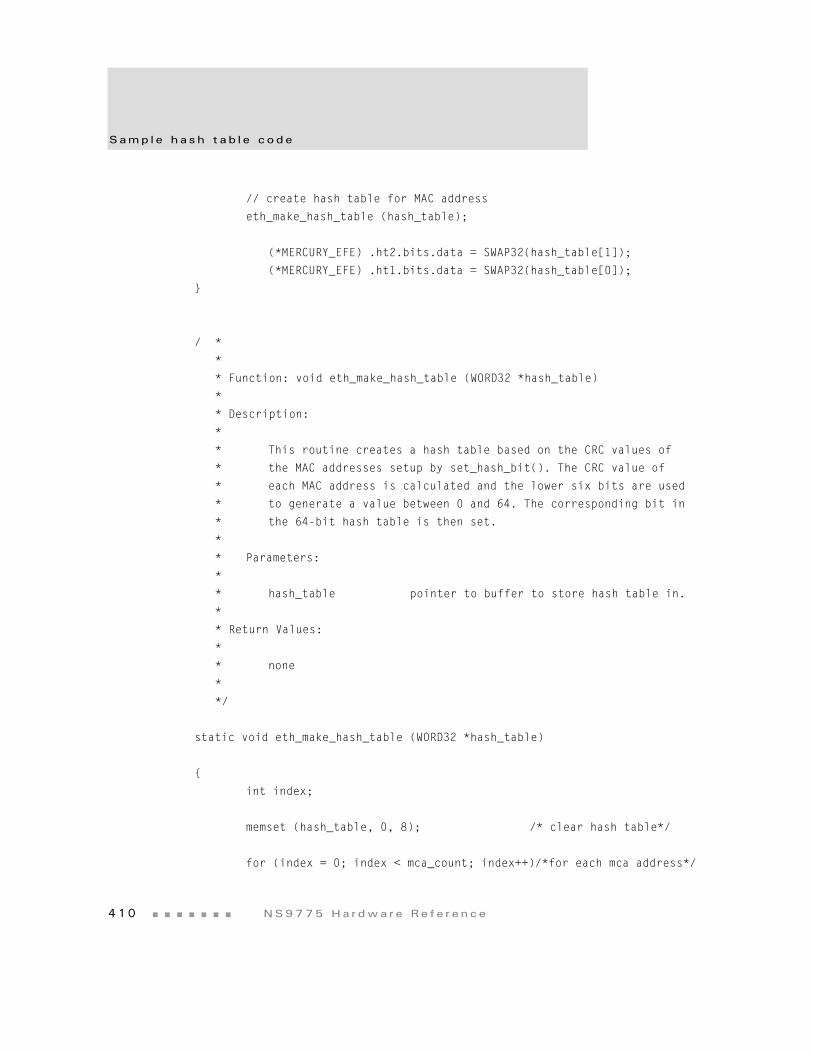
Samp l e ha sh t a b l e code
4 1 0 NS9775 Ha r dwa r e Re f e r ence
// create hash table for MAC address
eth_make_hash_table (hash_table);
(*MERCURY_EFE) .ht2.bits.data = SWAP32(hash_table[1]);
(*MERCURY_EFE) .ht1.bits.data = SWAP32(hash_table[0]);
}
/ *
*
* Function: void eth_make_hash_table (WORD32 *hash_table)
*
* Description:
*
* This routine creates a hash table based on the CRC values of
* the MAC addresses setup by set_hash_bit(). The CRC value of
* each MAC address is calculated and the lower six bits are used
* to generate a value between 0 and 64. The corresponding bit in
* the 64-bit hash table is then set.
*
* Parameters:
*
* hash_table pointer to buffer to store hash table in.
*
* Return Values:
*
* none
*
*/
static void eth_make_hash_table (WORD32 *hash_table)
{
int index;
memset (hash_table, 0, 8); /* clear hash table*/
for (index = 0; index < mca_count; index++)/*for each mca address*/
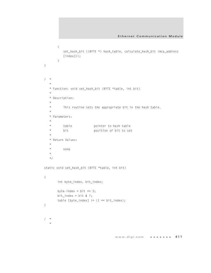
www.d i g i . com 411
E t he r n e t Commun i c a t i o n Modu l e
{
set_hash_bit ((BYTE *) hash_table, calculate_hash_bit (mca_address
[index]));
}
}
/ *
*
* Function: void set_hash_bit (BYTE *table, int bit)
*
* Description:
*
* This routine sets the appropriate bit in the hash table.
*
* Parameters:
*
* table pointer to hash table
* bit position of bit to set
*
* Return Values:
*
* none
*
*/
static void set_hash_bit (BYTE *table, int bit)
{
int byte_index, bit_index;
byte-index = bit >> 3;
bit_index = bit & 7;
table [byte_index] |= (1 << bit_index);
}
/ *
*
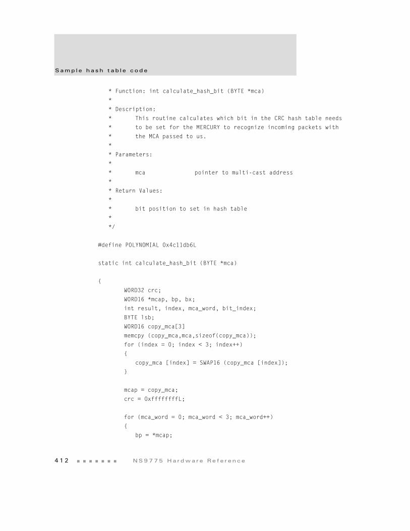
Samp l e ha sh t a b l e code
4 1 2 NS9775 Ha r dwa r e Re f e r ence
* Function: int calculate_hash_bit (BYTE *mca)
*
* Description:
* This routine calculates which bit in the CRC hash table needs
* to be set for the MERCURY to recognize incoming packets with
* the MCA passed to us.
*
* Parameters:
*
* mca pointer to multi-cast address
*
* Return Values:
*
* bit position to set in hash table
*
*/
#define POLYNOMIAL 0x4c11db6L
static int calculate_hash_bit (BYTE *mca)
{
WORD32 crc;
WORD16 *mcap, bp, bx;
int result, index, mca_word, bit_index;
BYTE lsb;
WORD16 copy_mca[3]
memcpy (copy_mca,mca,sizeof(copy_mca));
for (index = 0; index < 3; index++)
{
copy_mca [index] = SWAP16 (copy_mca [index]);
}
mcap = copy_mca;
crc = 0xffffffffL;
for (mca_word = 0; mca_word < 3; mca_word++)
{
bp = *mcap;
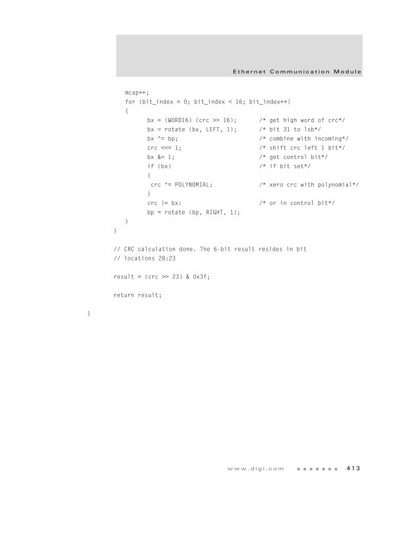
www.d i g i . com 413
E t he r n e t Commun i c a t i o n Modu l e
mcap++;
for (bit_index = 0; bit_index < 16; bit_index++)
{
bx = (WORD16) (crc >> 16); /* get high word of crc*/
bx = rotate (bx, LEFT, 1); /* bit 31 to lsb*/
bx ^= bp; /* combine with incoming*/
crc <<= 1; /* shift crc left 1 bit*/
bx &= 1; /* get control bit*/
if (bx) /* if bit set*/
{
crc ^= POLYNOMIAL; /* xero crc with polynomial*/
}
crc |= bx: /* or in control bit*/
bp = rotate (bp, RIGHT, 1);
}
}
// CRC calculation done. The 6-bit result resides in bit
// locations 28:23
result = (crc >> 23) & 0x3f;
return result;
}

415
PCI-to-AHB BridgeC H A P T E R 7
The PCI-to-AHB bridge provides connections between PCI-based modules/devices and the NS9775 AHB bus.
Important: This chapter presumes knowledge of PCI system standards and architecture, and explains how PCI works in relation to the AHB bus. If you have questions regarding PCI terminology or concepts, please refer to your PCI documentation.
Abou t t h e PC I - t o -AHB B r i dg e
4 1 6 NS9775 Ha r dwa r e Re f e r ence
About the PCI-to-AHB Bridge
The PCI-to-AHB bridge provides these features:
Supports PCI specification 2.1 and 2.2 protocol
AHB master and slave interfaces
PCI master and target interfaces
Open drain interrupt output for PCI bus
Interrupt to AHB bus for AHB and PCI bus errors
Supports 32-bit address and data on both busses
Supports AHB core clock up to 100 MHz, and a PCI core clock of 33 MHz
Performs all AHB-to-PCI reads as SPLIT transactions on the AHB bus (improves bus use)
Supports AHB burst transfers up to 8 words
AHB master supports all AHB slave responses for upstream (initiated on the PCI bus) PCI-to-AHB traffic
Supports early burst termination on the AHB bus
Dual 64-byte write buffers in both directions
Single 64-byte read buffers in both directions
Supports PCI configuration cycles
Supports target retry, target disconnect, and target abort on PCI bus
Supports all PCI parity generation and parity error detection
Includes all PCI-specific configuration registers
Supports configuration of internal PCI configuration registers using the AHB bus
Supports PCI-to-AHB address translation
Supports AHB-to-PCI address translation
Note: Use the AHB DMA function to move blocks of data between the ARM CPU and the PCI bus. Do not use load and store multiple commands to thePCI-to- AHB bridge and do not cache PCI memory.
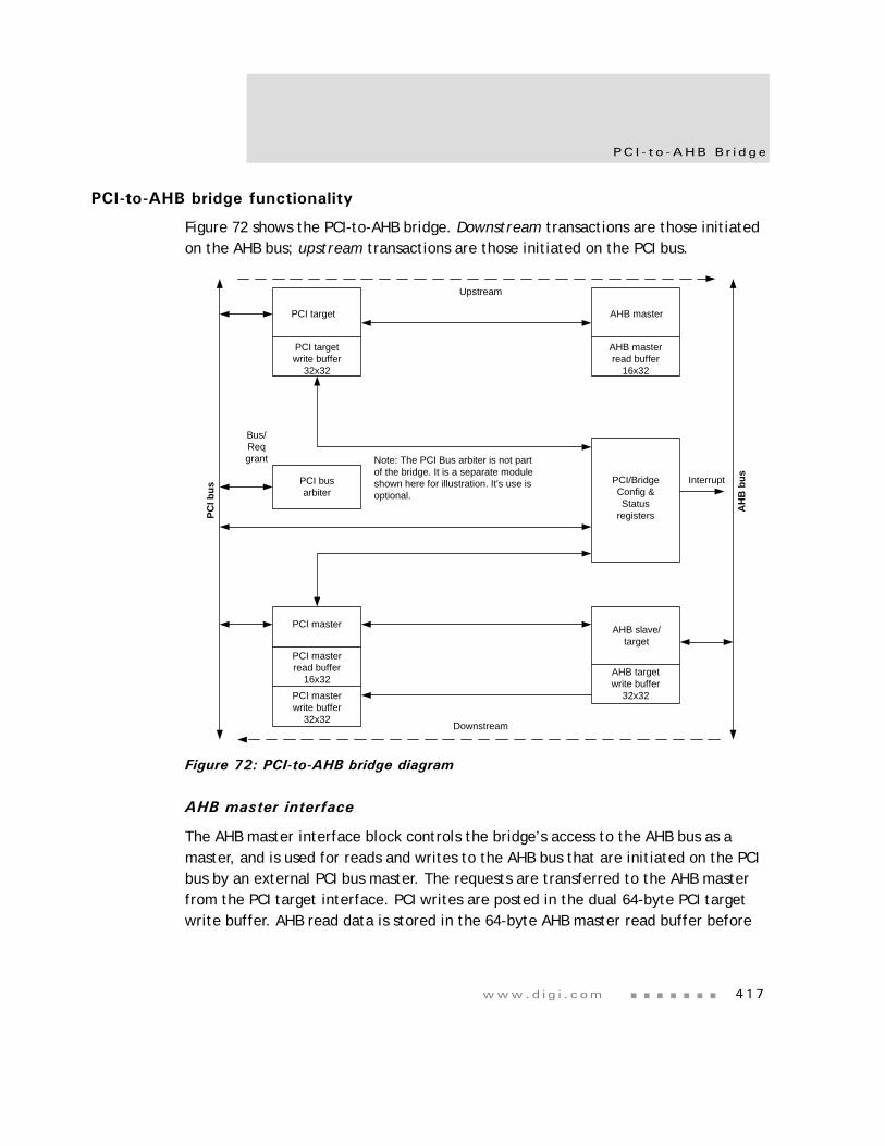
www.d i g i . com 417
PC I - t o -AHB B r i d ge
PCI-to-AHB bridge functionality
Figure 72 shows the PCI-to-AHB bridge. Downstream transactions are those initiated on the AHB bus; upstream transactions are those initiated on the PCI bus.
Figure 72: PCI-to-AHB bridge diagram
AHB master interface
The AHB master interface block controls the bridge’s access to the AHB bus as a master, and is used for reads and writes to the AHB bus that are initiated on the PCI bus by an external PCI bus master. The requests are transferred to the AHB master from the PCI target interface. PCI writes are posted in the dual 64-byte PCI target write buffer. AHB read data is stored in the 64-byte AHB master read buffer before
PCI target
PCI targetwrite buffer
32x32
PCI busarbiter
PCI/BridgeConfig &Status
registers
AHB master
AHB masterread buffer
16x32
AHB slave/target
AHB targetwrite buffer
32x32
PCI masterread buffer
16x32PCI masterwrite buffer
32x32
PCI master
Downstream
Upstream
Bus/Reqgrant
Interrupt
Note: The PCI Bus arbiter is not partof the bridge. It is a separate moduleshown here for illustration. It's use isoptional.
PCI b
us
AH
B b
us
Abou t t h e PC I - t o -AHB B r i dg e
4 1 8 NS9775 Ha r dwa r e Re f e r ence
being sent back to the PCI bus. The AHB master interface supports both single and burst transactions.
AHB slave/target interface
The AHB slave/target interface block controls the AHB target access to the bridge, and is used for reads and writes to the PCI bus that are initiated on the AHB bus. The requests are transferred to the PCI master interface. Writes are posted in the dual 64-byte AHB target write buffer and then transferred to the dual 64-byte PCI master write buffer. Reads are delayed through the AHB SPLIT transaction protocol. Read data is stored in the 64-byte PCI master read buffer. The AHB slave/target interface supports both single and burst transactions.
The AHB slave provides the AHB interface to the PCI/Bridge configuration registers (see page 423), using the CONFIG_ADDR and CONFIG_DATA memory spaces.
PCI target interface
The PCI target interface block controls the PCI bus access to the AHB bus, and is used for reads and writes that are initiated on the PCI bus by an external PCI bus master. The requests are transferred to the AHB master interface. Writes are posted in the dual 64-byte PCI target write buffer. The PCI target interface supports both single and burst transactions.
PCI master interface
The PCI master interface block controls the bridge’s access to the PCI bus as a master, and is used for reads and writes to the PCI bus that are initiated on the AHB bus. The PCI master interfaces to the AHB slave/target interface, and receives its requests from the AHB target interface. The PCI master has both a 64-byte read buffer and a dual 64-byte write buffer. Both single and burst transactions are supported.
PCI/bridge configuration and status registers
The PCI/bridge configuration and status registers block contains standard PCI configuration and status registers. All registers can be accessed using the PCI and AHB buses (see "Configuration registers," beginning on page 423).
www.d i g i . com 419
PC I - t o -AHB B r i d ge
PCI bus arbiter
The PCI bus arbiter (also referred to as PCI arbiter), although embedded in NS9775, is not part of the PCI-to-AHB bridge protocol. See "PCI bus arbiter," beginning on page 431, for information about the PCI arbiter. The arbiter’s use is optional.
Cross-bridge transaction error handling
The PCI-to-AHB bridge supports several error-handling mechanisms. All mechanisms can cause an interrupt to the system unless they are masked. Table 257 describes the errors and resulting action.
Error Action taken
PCI-to-AHB writeA write to the AHB bus does not complete due to receipt of an AHB bus error
The AHBERR bit in the PCI Bridge Interrupt Status register is set.
The AHB address is stored in the AHB Error Address register in the bridge.
PCI-to-AHB readA read to the AHB bus does not complete due to receipt of an AHB bus error
The AHBERR bit in the PCI Bridge Interrupt Status register is set.
The AHB address is stored in the AHB Error Address register in the bridge.
A PCI target abort is issued to release the PCI bus
The SIGNALED TARGET ABORT bit in the PCI Status register is set.
AHB-to-PCI writeA write to the PCI bus does not complete due to receipt of a PCI bus error.
Bits [15:11] and [04] in the PCI Status register will indicate the source of the PCI bus error.
The PCI address is stored in the PCI Error Address register in the bridge.
AHB-to-PCI readA read to the PCI bus does not complete due to receipt of a PCI bus error.
Bits [15:11] and [04] in the PCI Status register will indicate the source of the PCI bus error
The PCI address is stored in the PCI Error Address register in the bridge.
Table 257: PCI-to-AHB error handling
Abou t t h e PC I - t o -AHB B r i dg e
4 2 0 NS9775 Ha r dwa r e Re f e r ence
PCI target error filtering
If the PCI target address or data parity checking logic finds an error during upstream transactions, the transaction is not passed to the AHB master. In this situation, the DETECTED PARITY ERROR bit in the PCI Status register is set. For address parity errors, the SIGNALED TARGET ABORT bit in the PCI Status register is set.
For data parity checking on writes, the entire burst is discarded if any word in the burst has a parity error.
AHB address decoding and translation
The PCI-to-AHB bridge supports these four AHB address spaces:
PCI memory (0x8000_0000->0x8FFF_FFFF; 256 MB)
PCI IO (0xA000_0000->0xA00F_FFFF; 1 MB)
PCI CONFIG_ADDR register (0xA010_0000)
PCI CONFIG_DATA register (0xA020_0000)
The bridge supports AHB to PCI memory address translation using the PCI Bridge AHB to PCI Memory Address Translate 0/1 (see page 449 and page 450) and PCI Bridge Address Translation Control (see page 453) registers. The address translation scheme breaks the 256 MB memory window from AHB to PCI into eight 32 MB subwindows that can be translated individually.
The PALTxVAL fields in the PCI Bridge AHB to PCI Memory Address Translate 0/1 registers control the translation for each of the eight subwindows. For example, if PALT0VAL is set to 0x75, an access to 0x8000_0000 on the AHB bus is mapped to 0xEA00_0000 in the PCI bus. The PALT_EN bit in the PCI Bridge Address Translation Control register determines whether AHB to PCI address translation is enabled:
When set to 1, PALT_EN enables address translation.
When set to 0, no address translation takes place, and the AHB and PCI addresses are identical.
Address translation also is provided for accesses to PCI IO space from the AHB bus. The translation process is similar to memory address translation, with this exception: the PALT8VAL field translates the 1 MB window dedicated to PCI IO space to another 1 MB IO window on the PCI bus. When PALT_EN is set to 1, IO translation is enabled.
www.d i g i . com 421
PC I - t o -AHB B r i d ge
PCI address decoding and mapping
The PCI-to-AHB bridge uses six Base Address registers (BAR), defined in the PCI Configuration register (see Table 260, “PCI/bridge configuration registers,” on page 425), to determine the range of PCI addresses to which the bridge responds. The window size of each Base Address register is hardwired (see Table 263 on page 429), but each register can be enabled or disabled using the ENBAR0–ENBAR5 bits in the PCI Miscellaneous Support register (see page 438) in the PCI arbiter.
The bridge supports PCI to AHB memory address translation using the PCI Bridge PCI to AHB Memory Address Translate 0/1(see page 451) and PCI Bridge Address Translation Control (see page 453) registers. The address translation scheme provides a separate translation value for each of the six Base Address registers. The translation window size is the same as the size of the corresponding register.
The MALTxVAL fields in the PCI Bridge PCI to AHB Memory Address Translate 0/1 registers (see page 451 and page 452) control the translation for each of the six Base Address registers. For example, if MALT1VAL is set to 0x08, an access to 0xFC00_0000 on the PCI bus that hits Base Address register 1 is mapped to 0x2000_0000 on the AHB bus. The MALT_EN bit in the PCI Bridge Address Translation Control register determines whether PCI to AHB address translation is enabled:
When set to 1, MALT_EN enables address translation.
When set to 0, no address translation takes place, and the AHB and PCI addresses are identical.
The external PCI bus is allowed access only to NS9775’s system memory. The MALTxVAL values, therefore, should be programmed only to map addresses in the lower 2 GB of NS9775’s 4 GB address space (0x0000_0000 -> 0x7FFF_FFFF)
Interrupts
The bridge generates an interrupt to the AHB bus, for either AHB or PCI bus errors. An AHB bus error interrupt is generated when the AHB master receives an ERROR response to a transaction it initiated. The status bit for this interrupt, AHBERR, is in the PCI Bridge Interrupt Status register (see page 446).
A PCI bus error interrupt is generated for any of these PCI conditions:
Address or data parity error detected (DPE, see "Detected parity error" on page 427)
Abou t t h e PC I - t o -AHB B r i dg e
4 2 2 NS9775 Ha r dwa r e Re f e r ence
Bridge-generated system error (SERR#, see "Signaled system error" on page 427)
Bridge receives a master abort (RMA, see "Received master abort" on page 427)
Bridge receives a target abort (RTA, see "Received target abort" on page 427)
Bridge signals a target abort (STA, see "Signaled target abort" on page 428)
Bridge master finds a parity error on read data or detects the target asserting a master data parity error (PERR#, see "Master data parity error" on page 428) and the parity error response bit in the PCI Command register (see page 426) is set.
The PCI Status register (see page 427) contains the status bits for the interrupts caused by PCI bus errors.
Use the PCI Bridge Interrupt Enable register (see page 447) to enable or disable interrupt sources. Clearing an enable bit (setting the bit to 0) prevents the associated interrupt status bit from asserting the external interrupt to the system.
When an AHB bus error occurs, the AHB address that caused the bus error is saved in the AHB Address Error register (see "PCI Bridge AHB Error Address register" on page 445). Because multiple errors can occur before the software services the interrupt, no new addresses are saved in the register until AHBERR (in the PCI Bridge Interrupt Status register) is cleared.
When a PCI bus error occurs, the PCI address that caused the bus error is saved in the PCI Address Error register ("PCI Bridge PCI Error Address register" on page 446). Because multiple bus errors can occur before the software services the interrupt, no new addresses are saved in the register until all error bits are cleared in the PCI Status register.
The bridge can drive an interrupt to the PCI bus. This interrupt is driven from the INTA2PCI bit in the PCI Miscellaneous Support register (see page 438) in the PCI arbiter. This interrupt is used only in systems in which NS9775 is not processing PCI interrupts, and is set by software.
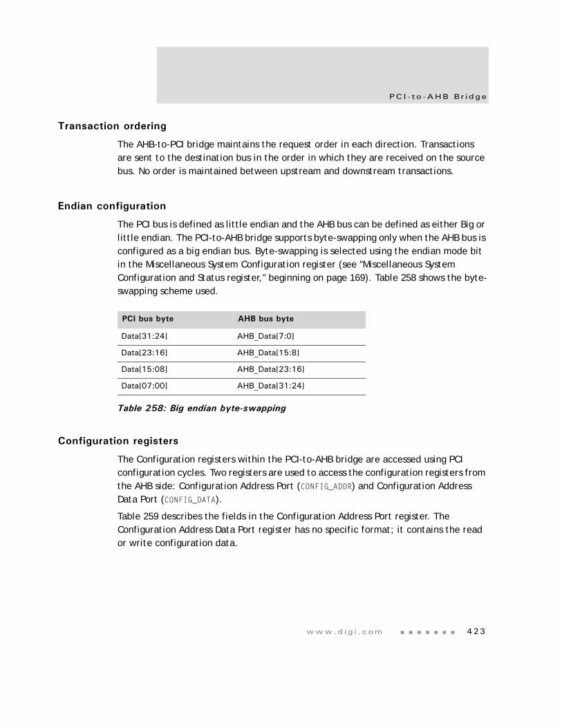
www.d i g i . com 423
PC I - t o -AHB B r i d ge
Transaction ordering
The AHB-to-PCI bridge maintains the request order in each direction. Transactions are sent to the destination bus in the order in which they are received on the source bus. No order is maintained between upstream and downstream transactions.
Endian configuration
The PCI bus is defined as little endian and the AHB bus can be defined as either Big or little endian. The PCI-to-AHB bridge supports byte-swapping only when the AHB bus is configured as a big endian bus. Byte-swapping is selected using the endian mode bit in the Miscellaneous System Configuration register (see "Miscellaneous System Configuration and Status register," beginning on page 169). Table 258 shows the byte-swapping scheme used.
Configuration registers
The Configuration registers within the PCI-to-AHB bridge are accessed using PCI configuration cycles. Two registers are used to access the configuration registers from the AHB side: Configuration Address Port (CONFIG_ADDR) and Configuration Address Data Port (CONFIG_DATA).
Table 259 describes the fields in the Configuration Address Port register. The Configuration Address Data Port register has no specific format; it contains the read or write configuration data.
PCI bus byte AHB bus byte
Data[31:24] AHB_Data[7:0]
Data[23:16] AHB_Data[15:8]
Data[15:08] AHB_Data[23:16]
Data[07:00] AHB_Data[31:24]
Table 258: Big endian byte-swapping
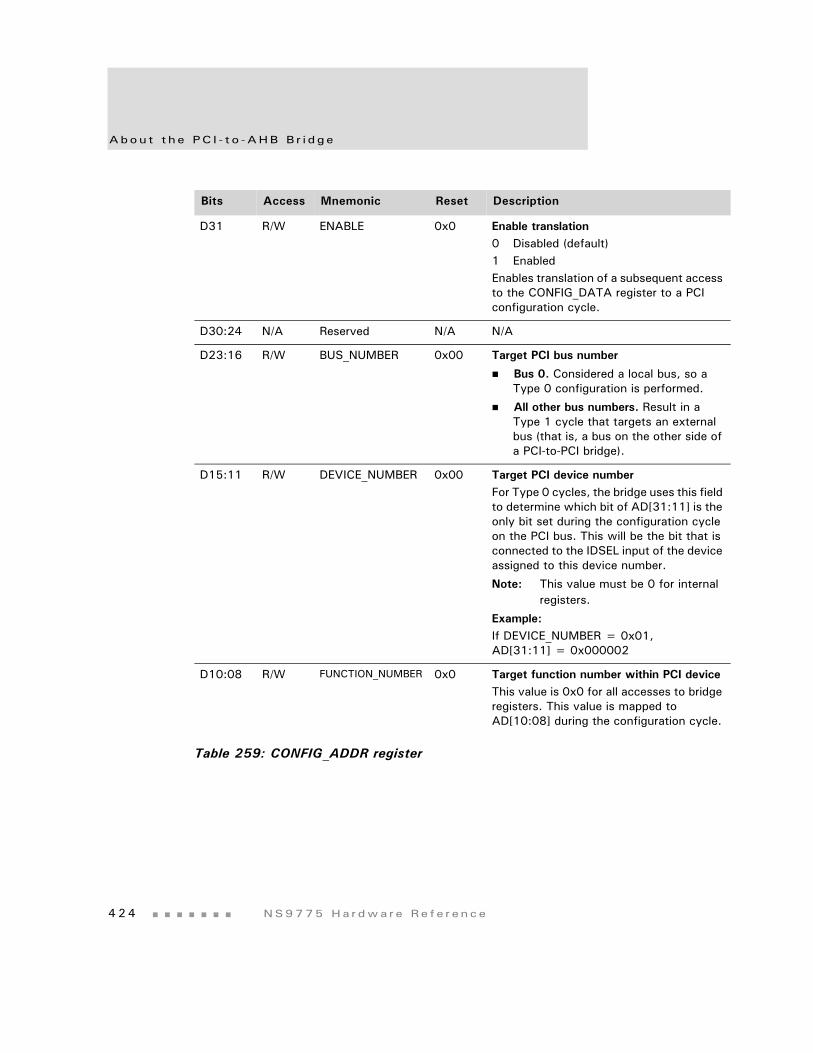
Abou t t h e PC I - t o -AHB B r i dg e
4 2 4 NS9775 Ha r dwa r e Re f e r ence
Bits Access Mnemonic Reset Description
D31 R/W ENABLE 0x0 Enable translation0 Disabled (default)1 EnabledEnables translation of a subsequent access to the CONFIG_DATA register to a PCI configuration cycle.
D30:24 N/A Reserved N/A N/A
D23:16 R/W BUS_NUMBER 0x00 Target PCI bus number
Bus 0. Considered a local bus, so a Type 0 configuration is performed.
All other bus numbers. Result in a Type 1 cycle that targets an external bus (that is, a bus on the other side of a PCI-to-PCI bridge).
D15:11 R/W DEVICE_NUMBER 0x00 Target PCI device numberFor Type 0 cycles, the bridge uses this field to determine which bit of AD[31:11] is the only bit set during the configuration cycle on the PCI bus. This will be the bit that is connected to the IDSEL input of the device assigned to this device number.
Note: This value must be 0 for internal registers.
Example:If DEVICE_NUMBER = 0x01, AD[31:11] = 0x000002
D10:08 R/W FUNCTION_NUMBER 0x0 Target function number within PCI deviceThis value is 0x0 for all accesses to bridge registers. This value is mapped to AD[10:08] during the configuration cycle.
Table 259: CONFIG_ADDR register
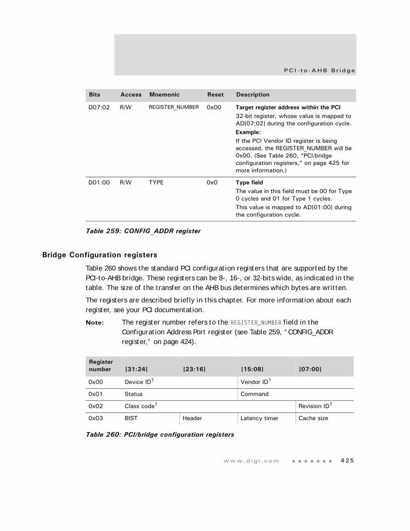
www.d i g i . com 425
PC I - t o -AHB B r i d ge
Bridge Configuration registers
Table 260 shows the standard PCI configuration registers that are supported by the PCI-to-AHB bridge. These registers can be 8-, 16-, or 32-bits wide, as indicated in the table. The size of the transfer on the AHB bus determines which bytes are written.
The registers are described briefly in this chapter. For more information about each register, see your PCI documentation.
Note: The register number refers to the REGISTER_NUMBER field in the Configuration Address Port register (see Table 259, “CONFIG_ADDR register,” on page 424).
D07:02 R/W REGISTER_NUMBER 0x00 Target register address within the PCI32-bit register, whose value is mapped to AD[07:02] during the configuration cycle. Example: If the PCI Vendor ID register is being accessed, the REGISTER_NUMBER will be 0x00. (See Table 260, “PCI/bridge configuration registers,” on page 425 for more information.)
D01:00 R/W TYPE 0x0 Type fieldThe value in this field must be 00 for Type 0 cycles and 01 for Type 1 cycles. This value is mapped to AD[01:00] during the configuration cycle.
Bits Access Mnemonic Reset Description
Table 259: CONFIG_ADDR register
Register number [31:24] [23:16] [15:08] [07:00]
0x00 Device ID1 Vendor ID1
0x01 Status Command
0x02 Class code1 Revision ID1
0x03 BIST Header Latency timer Cache size
Table 260: PCI/bridge configuration registers
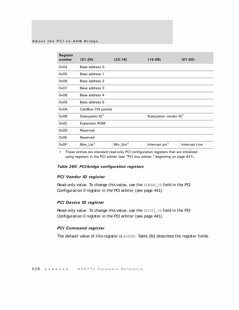
Abou t t h e PC I - t o -AHB B r i dg e
4 2 6 NS9775 Ha r dwa r e Re f e r ence
PCI Vendor ID register
Read-only value. To change this value, use the VENDOR_ID field in the PCI Configuration 0 register in the PCI arbiter (see page 441).
PCI Device ID register
Read-only value. To change this value, use the DEVICE_ID field in the PCI Configuration 0 register in the PCI arbiter (see page 441).
PCI Command register
The default value of this register is 0x0000. Table 261 describes the register fields.
0x04 Base address 0
0x05 Base address 1
0x06 Base address 2
0x07 Base address 3
0x08 Base address 4
0x09 Base address 5
0x0A CardBus CIS pointer
0x0B Subsystem ID1 Subsystem vendor ID1
0x0C Expansion ROM
0x0D Reserved
0x0E Reserved
0x0F Max_Lat1 Min_Gnt1 Interrupt pin1 Interrupt Line
1 These entries are standard read-only PCI configuration registers that are initialized using registers in the PCI arbiter (see "PCI bus arbiter," beginning on page 431).
Register number [31:24] [23:16] [15:08] [07:00]
Table 260: PCI/bridge configuration registers
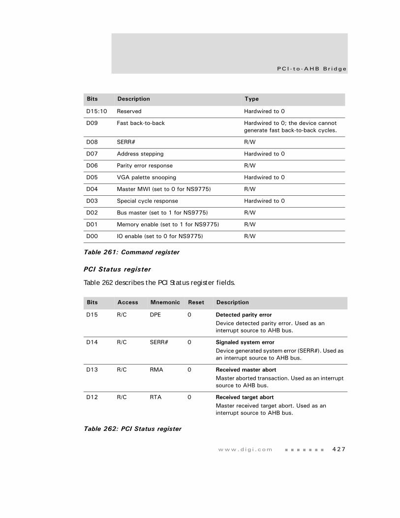
www.d i g i . com 427
PC I - t o -AHB B r i d ge
PCI Status register
Table 262 describes the PCI Status register fields.
Bits Description Type
D15:10 Reserved Hardwired to 0
D09 Fast back-to-back Hardwired to 0; the device cannot generate fast back-to-back cycles.
D08 SERR# R/W
D07 Address stepping Hardwired to 0
D06 Parity error response R/W
D05 VGA palette snooping Hardwired to 0
D04 Master MWI (set to 0 for NS9775) R/W
D03 Special cycle response Hardwired to 0
D02 Bus master (set to 1 for NS9775) R/W
D01 Memory enable (set to 1 for NS9775) R/W
D00 IO enable (set to 0 for NS9775) R/W
Table 261: Command register
Bits Access Mnemonic Reset Description
D15 R/C DPE 0 Detected parity errorDevice detected parity error. Used as an interrupt source to AHB bus.
D14 R/C SERR# 0 Signaled system errorDevice generated system error (SERR#). Used as an interrupt source to AHB bus.
D13 R/C RMA 0 Received master abortMaster aborted transaction. Used as an interrupt source to AHB bus.
D12 R/C RTA 0 Received target abortMaster received target abort. Used as an interrupt source to AHB bus.
Table 262: PCI Status register
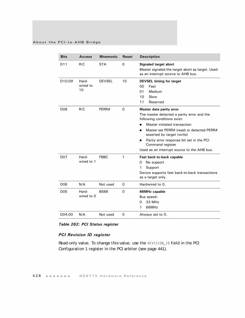
Abou t t h e PC I - t o -AHB B r i dg e
4 2 8 NS9775 Ha r dwa r e Re f e r ence
PCI Revision ID register
Read-only value. To change this value, use the REVISION_ID field in the PCI Configuration 1 register in the PCI arbiter (see page 441).
D11 R/C STA 0 Signaled target abortMaster signaled the target abort as target. Used as an interrupt source to AHB bus.
D10:09 Hard-wired to 10
DEVSEL 10 DEVSEL timing for target00 Fast01 Medium10 Slow11 Reserved
D08 R/C PERR# 0 Master data parity errorThe master detected a parity error and the following conditions exist:
Master initiated transaction
Master set PERR# (read) or detected PERR# asserted by target (write)
Parity error response bit set in the PCI Command register
Used as an interrupt source to the AHB bus.
D07 Hard-wired to 1
FBBC 1 Fast back-to-back capable0 No support1 SupportDevice supports fast back-to-back transactions as a target only.
D06 N/A Not used 0 Hardwired to 0.
D05 Hard-wired to 0
BS66 0 66MHz capableBus speed:0 33 MHz1 66MHz
D04:00 N/A Not used 0 Always set to 0.
Bits Access Mnemonic Reset Description
Table 262: PCI Status register
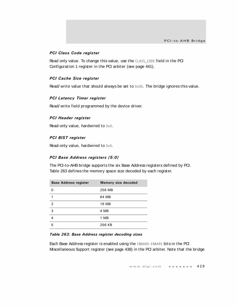
www.d i g i . com 429
PC I - t o -AHB B r i d ge
PCI Class Code register
Read only value. To change this value, use the CLASS_CODE field in the PCI Configuration 1 register in the PCI arbiter (see page 441).
PCI Cache Size register
Read/write value that should always be set to 0x00. The bridge ignores this value.
PCI Latency Timer register
Read/write field programmed by the device driver.
PCI Header register
Read-only value, hardwired to 0x0.
PCI BIST register
Read-only value, hardwired to 0x0.
PCI Base Address registers [5:0]
The PCI-to-AHB bridge supports the six Base Address registers defined by PCI. Table 263 defines the memory space size decoded by each register.
Each Base Address register is enabled using the ENBAR0–ENBAR5 bits in the PCI Miscellaneous Support register (see page 438) in the PCI arbiter. Note that the bridge
Base Address register Memory size decoded
0 256 MB
1 64 MB
2 16 MB
3 4 MB
4 1 MB
5 256 KB
Table 263: Base Address register decoding sizes
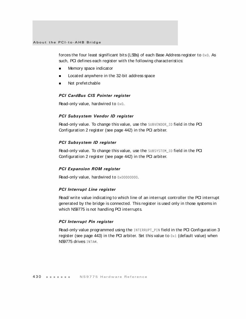
Abou t t h e PC I - t o -AHB B r i dg e
4 3 0 NS9775 Ha r dwa r e Re f e r ence
forces the four least significant bits (LSBs) of each Base Address register to 0x0. As such, PCI defines each register with the following characteristics:
Memory space indicator
Located anywhere in the 32-bit address space
Not prefetchable
PCI CardBus CIS Pointer register
Read-only value, hardwired to 0x0.
PCI Subsystem Vendor ID register
Read-only value. To change this value, use the SUBVENDOR_ID field in the PCI Configuration 2 register (see page 442) in the PCI arbiter.
PCI Subsystem ID register
Read-only value. To change this value, use the SUBSYSTEM_ID field in the PCI Configuration 2 register (see page 442) in the PCI arbiter.
PCI Expansion ROM register
Read-only value, hardwired to 0x00000000.
PCI Interrupt Line register
Read/write value indicating to which line of an interrupt controller the PCI interrupt generated by the bridge is connected. This register is used only in those systems in which NS9775 is not handling PCI interrupts.
PCI Interrupt Pin register
Read-only value programmed using the INTERRUPT_PIN field in the PCI Configuration 3 register (see page 443) in the PCI arbiter. Set this value to 0x1 (default value) when NS9775 drives INTA#.
www.d i g i . com 431
PC I - t o -AHB B r i d ge
PCI Min Grant register
Read-only value programmed using the MIN_GRANT field in the PCI Configuration 3 register (see page 443) in the PCI arbiter.
PCI Max Latency register
Read-only value programmed using the MAX_LATENCY field in the PCI Configuration 3 register (see page 443) in the PCI arbiter.
PCI bus arbiter
NS9775 provides an embedded PCI bus arbiter that supports up to three external PCI masters and the internal PCI-to-AHB bridge. The arbiter uses a rotating priority scheme. An AHB slave is integrated with the PCI bus arbiter to access programmable registers, to support system configuration and error reporting.
NS9775 can be configured to use either the embedded PCI arbiter or an external arbiter through the bootstrap initialization scheme used during powerup (see "Bootstrap initialization" on page 139). The RTCK pin selects the source of the arbiter:
The internal arbiter is used if RTCK = 1.
If a pulldown resistor is placed on the RTCK bit, an external arbiter is used. When an external arbiter is used, the REQ#/GNT# (request/grant) signals for the internal PCI-to-AHB bridge are brought to external pins on NS9775 (see Figure 74, "System connections to NS9775 — External arbiter and central resources," on page 471).
PCI arbiter functional description
The PCI bus arbiter supports up to four PCI masters, including the PCI-to-AHB bridge, using the rotating priority scheme shown in Table 264. With rotating priority, the priority of a master depends on its relative position to the last granted master. After reset, the arbiter defaults to the PCI-to-AHB bridge having the highest priority.
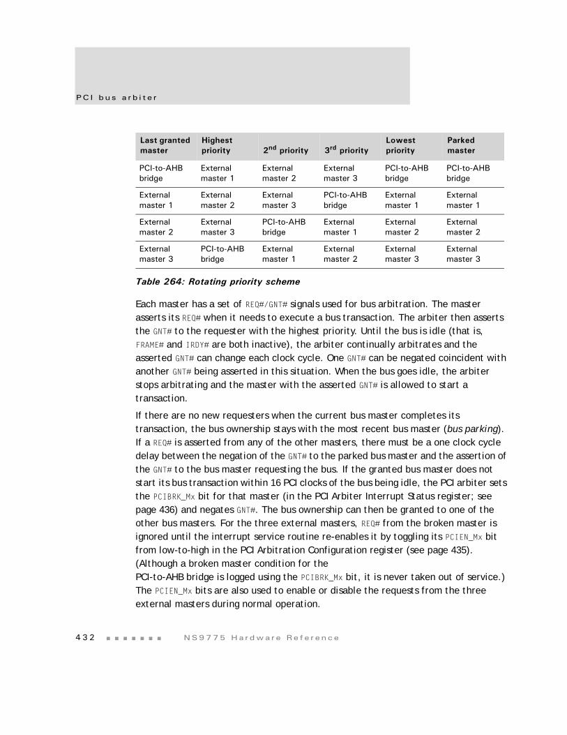
PC I bu s a r b i t e r
4 3 2 NS9775 Ha r dwa r e Re f e r ence
Each master has a set of REQ#/GNT# signals used for bus arbitration. The master asserts its REQ# when it needs to execute a bus transaction. The arbiter then asserts the GNT# to the requester with the highest priority. Until the bus is idle (that is, FRAME# and IRDY# are both inactive), the arbiter continually arbitrates and the asserted GNT# can change each clock cycle. One GNT# can be negated coincident with another GNT# being asserted in this situation. When the bus goes idle, the arbiter stops arbitrating and the master with the asserted GNT# is allowed to start a transaction.
If there are no new requesters when the current bus master completes its transaction, the bus ownership stays with the most recent bus master (bus parking). If a REQ# is asserted from any of the other masters, there must be a one clock cycle delay between the negation of the GNT# to the parked bus master and the assertion of the GNT# to the bus master requesting the bus. If the granted bus master does not start its bus transaction within 16 PCI clocks of the bus being idle, the PCI arbiter sets the PCIBRK_Mx bit for that master (in the PCI Arbiter Interrupt Status register; see page 436) and negates GNT#. The bus ownership can then be granted to one of the other bus masters. For the three external masters, REQ# from the broken master is ignored until the interrupt service routine re-enables it by toggling its PCIEN_Mx bit from low-to-high in the PCI Arbitration Configuration register (see page 435). (Although a broken master condition for thePCI-to-AHB bridge is logged using the PCIBRK_Mx bit, it is never taken out of service.) The PCIEN_Mx bits are also used to enable or disable the requests from the three external masters during normal operation.
Last granted master
Highest priority 2nd priority 3rd priority
Lowest priority
Parked master
PCI-to-AHB bridge
External master 1
External master 2
External master 3
PCI-to-AHB bridge
PCI-to-AHB bridge
External master 1
External master 2
External master 3
PCI-to-AHB bridge
External master 1
External master 1
External master 2
External master 3
PCI-to-AHB bridge
External master 1
External master 2
External master 2
External master 3
PCI-to-AHB bridge
External master 1
External master 2
External master 3
External master 3
Table 264: Rotating priority scheme
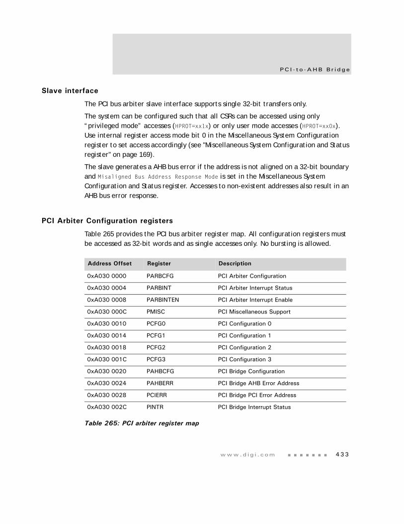
www.d i g i . com 433
PC I - t o -AHB B r i d ge
Slave interface
The PCI bus arbiter slave interface supports single 32-bit transfers only.
The system can be configured such that all CSRs can be accessed using only “privileged mode” accesses (HPROT=xx1x) or only user mode accesses (HPROT=xx0x). Use internal register access mode bit 0 in the Miscellaneous System Configuration register to set access accordingly (see "Miscellaneous System Configuration and Status register" on page 169).
The slave generates a AHB bus error if the address is not aligned on a 32-bit boundary and Misaligned Bus Address Response Mode is set in the Miscellaneous System Configuration and Status register. Accesses to non-existent addresses also result in an AHB bus error response.
PCI Arbiter Configuration registers
Table 265 provides the PCI bus arbiter register map. All configuration registers must be accessed as 32-bit words and as single accesses only. No bursting is allowed.
Address Offset Register Description
0xA030 0000 PARBCFG PCI Arbiter Configuration
0xA030 0004 PARBINT PCI Arbiter Interrupt Status
0xA030 0008 PARBINTEN PCI Arbiter Interrupt Enable
0xA030 000C PMISC PCI Miscellaneous Support
0xA030 0010 PCFG0 PCI Configuration 0
0xA030 0014 PCFG1 PCI Configuration 1
0xA030 0018 PCFG2 PCI Configuration 2
0xA030 001C PCFG3 PCI Configuration 3
0xA030 0020 PAHBCFG PCI Bridge Configuration
0xA030 0024 PAHBERR PCI Bridge AHB Error Address
0xA030 0028 PCIERR PCI Bridge PCI Error Address
0xA030 002C PINTR PCI Bridge Interrupt Status
Table 265: PCI arbiter register map
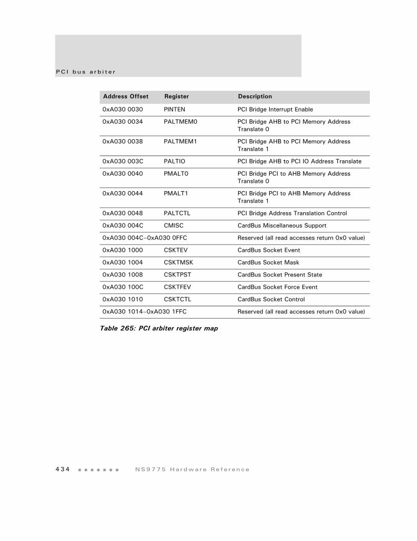
PC I bu s a r b i t e r
4 3 4 NS9775 Ha r dwa r e Re f e r ence
0xA030 0030 PINTEN PCI Bridge Interrupt Enable
0xA030 0034 PALTMEM0 PCI Bridge AHB to PCI Memory Address Translate 0
0xA030 0038 PALTMEM1 PCI Bridge AHB to PCI Memory Address Translate 1
0xA030 003C PALTIO PCI Bridge AHB to PCI IO Address Translate
0xA030 0040 PMALT0 PCI Bridge PCI to AHB Memory Address Translate 0
0xA030 0044 PMALT1 PCI Bridge PCI to AHB Memory Address Translate 1
0xA030 0048 PALTCTL PCI Bridge Address Translation Control
0xA030 004C CMISC CardBus Miscellaneous Support
0xA030 004C–0xA030 0FFC Reserved (all read accesses return 0x0 value)
0xA030 1000 CSKTEV CardBus Socket Event
0xA030 1004 CSKTMSK CardBus Socket Mask
0xA030 1008 CSKTPST CardBus Socket Present State
0xA030 100C CSKTFEV CardBus Socket Force Event
0xA030 1010 CSKTCTL CardBus Socket Control
0xA030 1014–0xA030 1FFC Reserved (all read accesses return 0x0 value)
Address Offset Register Description
Table 265: PCI arbiter register map
www.d i g i . com 435
PC I - t o -AHB B r i d ge
PCI Arbiter Configuration register
Address: A030 0000The PCI Arbiter Configuration register enables and disables each of the three external PCI bus masters. The internal PCI-to-AHB bridge is always enabled.
Register bit assignment
Bits Access Mnemonic Reset Description
D31:04 Read only; hard-wired to 0
Reserved N/A N/A
D03 R/W PCIEN_M3 0 External master 3 enable0 Disable (default)1 EnableIf the master becomes broken, toggle low -> high to re-enable.
D02 R/W PCIEN_M2 0 External master 2 enable0 Disable (default)1 EnableIf the master becomes broken, toggle low -> high to re-enable.
D01 R/W PCIEN_M1 0 External Master 1 Enable0 Disable (default)1 EnableIf the master becomes broken, toggle low-> high to re-enable.
Table 266: PCI Arbiter Configuration register
Reserved
PCIEN_M3
PCI_CTL_RSC_n
13 12 11 10 9 8 7 6 5 4 3 2 1 015 14
31 29 28 27 26 25 24 23 22 21 20 19 18 17 1630
ReservedPCIEN_M2
PCIEN_M1
PC I bu s a r b i t e r
4 3 6 NS9775 Ha r dwa r e Re f e r ence
PCI Arbiter Interrupt Status register
Address: A030 0004The PCI Arbiter Interrupt Status register reports broken masters (that is, masters that do not respond in 16 clocks after being granted the bus) and PCI system errors from external PCI agents (that is, SERR# asserted for 1 clock cycle). There is a separate bit for each of the interrupt sources, and each bit can cause an interrupt if the associated bit in the PCI Arbiter Interrupt Enable register is set to 1.
Note: For diagnostics, software can cause an interrupt by writing a 1 to a bit that is set to 0. Otherwise, in normal operation, the software writes a 1 to a bit that is set to clear the bit and the interrupt from the PCI arbiter.
Register bit assignment
D00 R PCI_CTL_RSC_n N/A PCI_CENTRAL_RSC_n input to NS9775 (NS9775 has internal pulldown)0 NS9775 provides PCI central resource
functions (pulldown)1 NS9775 does not provide PCI central
resource functions
Bits Access Mnemonic Reset Description
D31:06 Read only; hard-wired to 0
Reserved N/A N/A
Table 267: PCI Arbiter Interrupt Status register
Bits Access Mnemonic Reset Description
Table 266: PCI Arbiter Configuration register
Reserved
CCLKRUN
PCISERR
PCIBRK_M3
PCIBRK_M0
13 12 11 10 9 8 7 6 5 4 3 2 1 015 14
31 29 28 27 26 25 24 23 22 21 20 19 18 17 1630
ReservedPCI
BRK_M2
PCIBRK_M1
www.d i g i . com 437
PC I - t o -AHB B r i d ge
PCI Arbiter Interrupt Enable register
Address: A030 0008The PCI Arbiter Interrupt Enable register has an enable bit for each of the interrupt status bits in the PCI Arbiter Interrupt Status register. Set these bits to 1 to allow the associated interrupt status bit to cause an interrupt to the system.
Register bit assignment
D05 R/C CCLKRUN 0 Restart CardBus clockUsed for CardBus Applications only. Indicates that an external CardBus card has asserted CardBus CCLKRUN# to request that the CardBus clock be restarted.
D04 R/C PCISERR 0 An SERR signal has been received from an external PCI agent.
D03 R/C PCIBRK_M3 0 External master 3 broken
D02 R/C PCIBRK_M2 0 External master 2 broken
D01 R/C PCIBRK_M1 0 External master 1 broken
D00 R/C PCIBRK_M0 0 PCI-to-AHB bridge broken
BIts Access Mnemonic Reset Description
D31:06 Read only; hard-wired to 0
Reserved N/A N/A
Table 268: PCI Arbiter Interrupt Enable register
Bits Access Mnemonic Reset Description
Table 267: PCI Arbiter Interrupt Status register
Reserved
EN_CCLKRUN
EN_PCI
SERR
EN_PBRK_M3
EN_PBRK_M0
13 12 11 10 9 8 7 6 5 4 3 2 1 015 14
31 29 28 27 26 25 24 23 22 21 20 19 18 17 1630
ReservedEN_PBRK_M2
EN_PBRK_M1
PC I bu s a r b i t e r
4 3 8 NS9775 Ha r dwa r e Re f e r ence
PCI Miscellaneous Support register
Address: A030 000CThe PCI Miscellaneous Support register contains miscellaneous PCI functions that are required in NS9775.
Change the EN_BARx fields only during system initialization, when there is no PCI activity.
In a system where NS9775 is not the host, the EN_BARx fields must be programmed within 225 PCI clocks of RST# being negated. This is the time allowed from RST# negated to the first configuration cycle on the PCI bus.
D05 R/W EN_CCLKRUN 0 Enable CCLKRUN# interrupt0 Disable (default)1 Enable
D04 R/W EN_PCISERR 0 Enable SERR received from external PCI agent0 Disable (default)1 Enable
D03 R/W EN_PBRK_M3 0 Enable external master 3 broken0 Disable (default)1 Enable
D02 R/W EN_PBRK_M2 0 Enable external master 2 broken0 Disable (default)1 Enable
D01 R/W EN_PBRK_M1 0 Enable external master 1 broken0 Disable (default)1 Enable
D00 R/W EN_PBRK_M0 0 Enable PCI-to-AHB bridge broken0 Disable (default)1 Enable
BIts Access Mnemonic Reset Description
Table 268: PCI Arbiter Interrupt Enable register
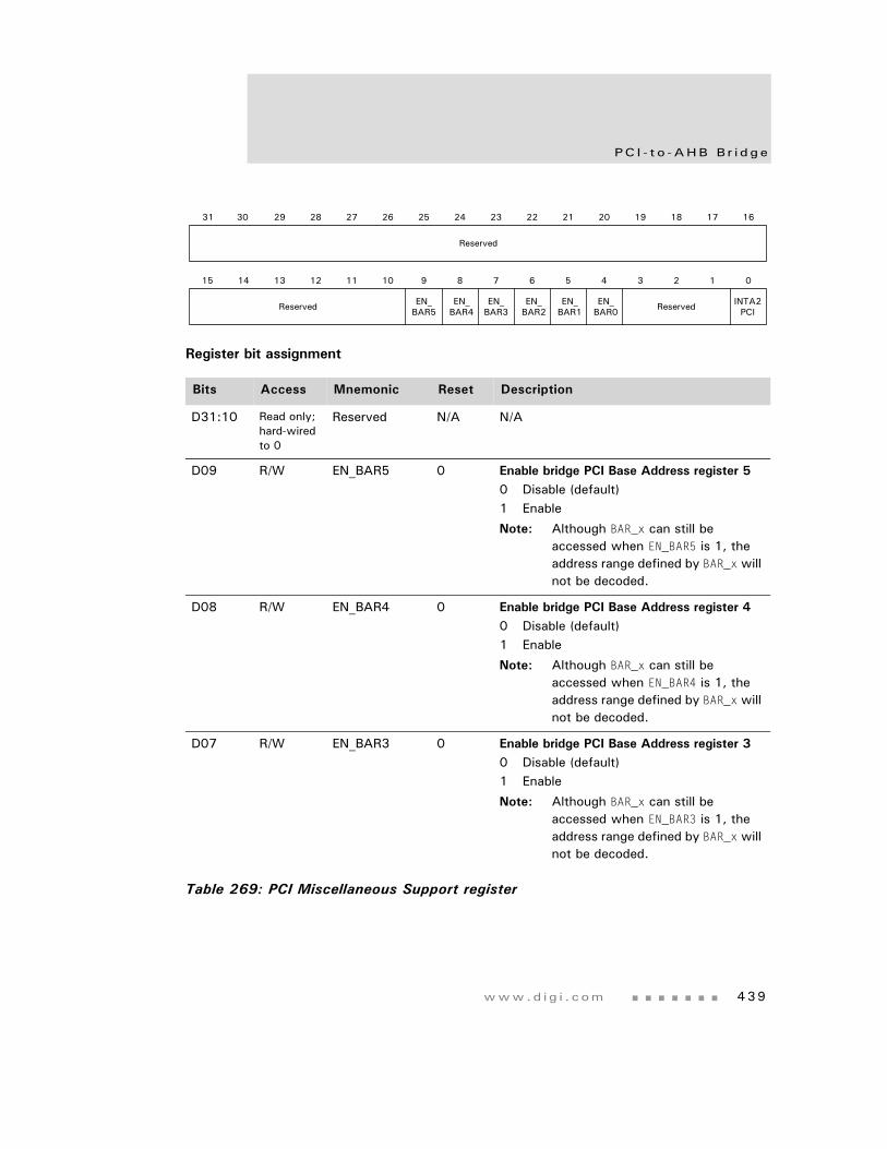
www.d i g i . com 439
PC I - t o -AHB B r i d ge
Register bit assignment
Bits Access Mnemonic Reset Description
D31:10 Read only; hard-wired to 0
Reserved N/A N/A
D09 R/W EN_BAR5 0 Enable bridge PCI Base Address register 50 Disable (default)1 Enable
Note: Although BAR_x can still be accessed when EN_BAR5 is 1, the address range defined by BAR_x will not be decoded.
D08 R/W EN_BAR4 0 Enable bridge PCI Base Address register 40 Disable (default)1 Enable
Note: Although BAR_x can still be accessed when EN_BAR4 is 1, the address range defined by BAR_x will not be decoded.
D07 R/W EN_BAR3 0 Enable bridge PCI Base Address register 30 Disable (default)1 Enable
Note: Although BAR_x can still be accessed when EN_BAR3 is 1, the address range defined by BAR_x will not be decoded.
Table 269: PCI Miscellaneous Support register
Reserved
EN_BAR1
EN_BAR0
INTA2PCI
13 12 11 10 9 8 7 6 5 4 3 2 1 015 14
31 29 28 27 26 25 24 23 22 21 20 19 18 17 1630
Reserved ReservedEN_BAR5
EN_BAR4
EN_BAR3
EN_BAR2
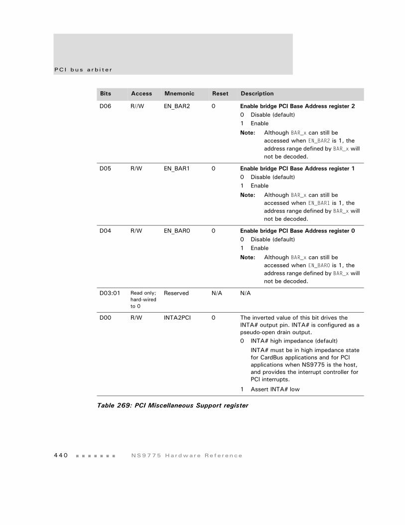
PC I bu s a r b i t e r
4 4 0 NS9775 Ha r dwa r e Re f e r ence
D06 R//W EN_BAR2 0 Enable bridge PCI Base Address register 20 Disable (default)1 Enable
Note: Although BAR_x can still be accessed when EN_BAR2 is 1, the address range defined by BAR_x will not be decoded.
D05 R/W EN_BAR1 0 Enable bridge PCI Base Address register 10 Disable (default)1 Enable
Note: Although BAR_x can still be accessed when EN_BAR1 is 1, the address range defined by BAR_x will not be decoded.
D04 R/W EN_BAR0 0 Enable bridge PCI Base Address register 00 Disable (default)1 Enable
Note: Although BAR_x can still be accessed when EN_BAR0 is 1, the address range defined by BAR_x will not be decoded.
D03:01 Read only; hard-wired to 0
Reserved N/A N/A
D00 R/W INTA2PCI 0 The inverted value of this bit drives the INTA# output pin. INTA# is configured as a pseudo-open drain output.0 INTA# high impedance (default)
INTA# must be in high impedance state for CardBus applications and for PCI applications when NS9775 is the host, and provides the interrupt controller for PCI interrupts.
1 Assert INTA# low
Bits Access Mnemonic Reset Description
Table 269: PCI Miscellaneous Support register
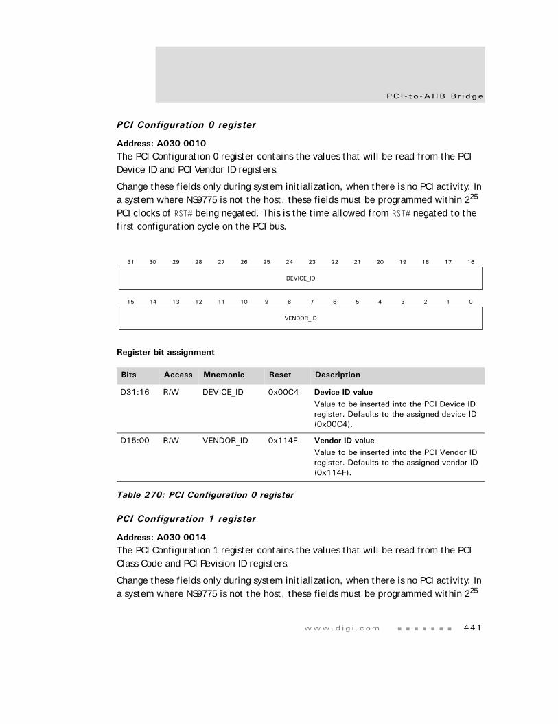
www.d i g i . com 441
PC I - t o -AHB B r i d ge
PCI Configuration 0 register
Address: A030 0010The PCI Configuration 0 register contains the values that will be read from the PCI Device ID and PCI Vendor ID registers.
Change these fields only during system initialization, when there is no PCI activity. In a system where NS9775 is not the host, these fields must be programmed within 225 PCI clocks of RST# being negated. This is the time allowed from RST# negated to the first configuration cycle on the PCI bus.
Register bit assignment
PCI Configuration 1 register
Address: A030 0014The PCI Configuration 1 register contains the values that will be read from the PCI Class Code and PCI Revision ID registers.
Change these fields only during system initialization, when there is no PCI activity. In a system where NS9775 is not the host, these fields must be programmed within 225
Bits Access Mnemonic Reset Description
D31:16 R/W DEVICE_ID 0x00C4 Device ID valueValue to be inserted into the PCI Device ID register. Defaults to the assigned device ID (0x00C4).
D15:00 R/W VENDOR_ID 0x114F Vendor ID valueValue to be inserted into the PCI Vendor ID register. Defaults to the assigned vendor ID (0x114F).
Table 270: PCI Configuration 0 register
DEVICE_ID
13 12 11 10 9 8 7 6 5 4 3 2 1 015 14
31 29 28 27 26 25 24 23 22 21 20 19 18 17 1630
VENDOR_ID
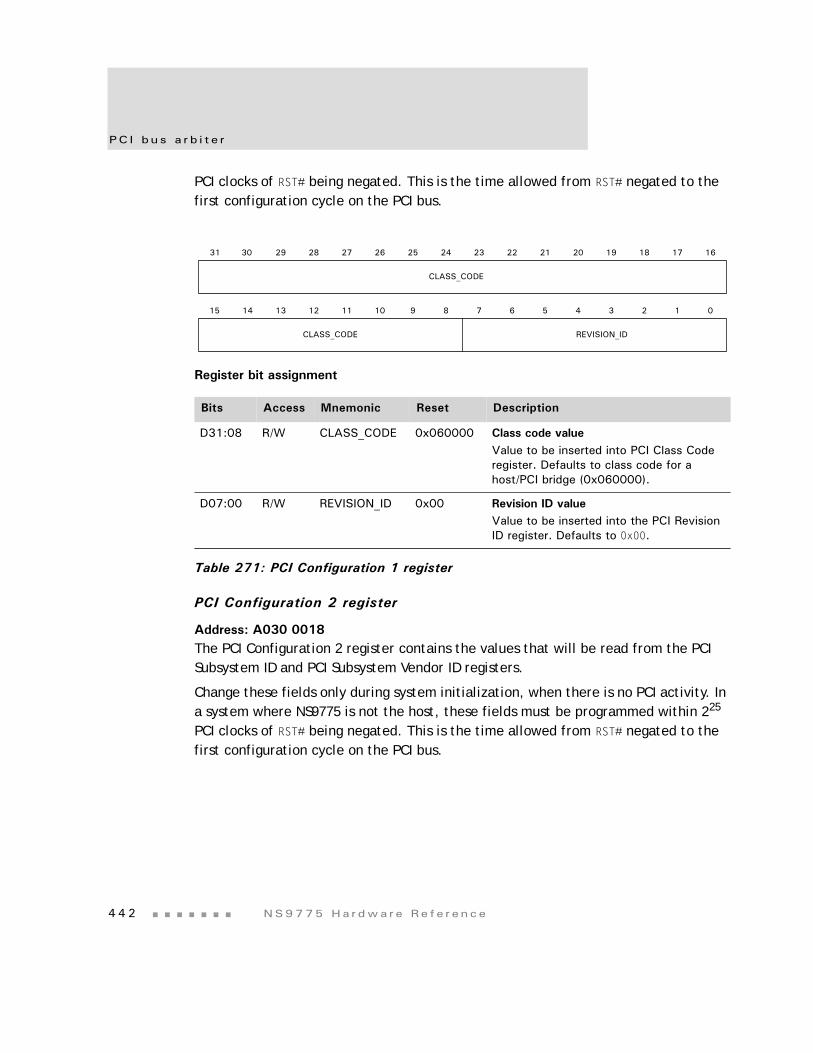
PC I bu s a r b i t e r
4 4 2 NS9775 Ha r dwa r e Re f e r ence
PCI clocks of RST# being negated. This is the time allowed from RST# negated to the first configuration cycle on the PCI bus.
Register bit assignment
PCI Configuration 2 register
Address: A030 0018The PCI Configuration 2 register contains the values that will be read from the PCI Subsystem ID and PCI Subsystem Vendor ID registers.
Change these fields only during system initialization, when there is no PCI activity. In a system where NS9775 is not the host, these fields must be programmed within 225 PCI clocks of RST# being negated. This is the time allowed from RST# negated to the first configuration cycle on the PCI bus.
Bits Access Mnemonic Reset Description
D31:08 R/W CLASS_CODE 0x060000 Class code valueValue to be inserted into PCI Class Code register. Defaults to class code for a host/PCI bridge (0x060000).
D07:00 R/W REVISION_ID 0x00 Revision ID valueValue to be inserted into the PCI Revision ID register. Defaults to 0x00.
Table 271: PCI Configuration 1 register
CLASS_CODE
13 12 11 10 9 8 7 6 5 4 3 2 1 015 14
31 29 28 27 26 25 24 23 22 21 20 19 18 17 1630
CLASS_CODE REVISION_ID
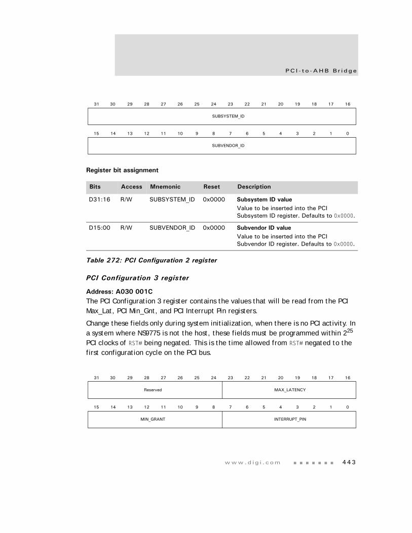
www.d i g i . com 443
PC I - t o -AHB B r i d ge
Register bit assignment
PCI Configuration 3 register
Address: A030 001CThe PCI Configuration 3 register contains the values that will be read from the PCI Max_Lat, PCI Min_Gnt, and PCI Interrupt Pin registers.
Change these fields only during system initialization, when there is no PCI activity. In a system where NS9775 is not the host, these fields must be programmed within 225 PCI clocks of RST# being negated. This is the time allowed from RST# negated to the first configuration cycle on the PCI bus.
Bits Access Mnemonic Reset Description
D31:16 R/W SUBSYSTEM_ID 0x0000 Subsystem ID valueValue to be inserted into the PCI Subsystem ID register. Defaults to 0x0000.
D15:00 R/W SUBVENDOR_ID 0x0000 Subvendor ID valueValue to be inserted into the PCI Subvendor ID register. Defaults to 0x0000.
Table 272: PCI Configuration 2 register
SUBSYSTEM_ID
13 12 11 10 9 8 7 6 5 4 3 2 1 015 14
31 29 28 27 26 25 24 23 22 21 20 19 18 17 1630
SUBVENDOR_ID
Reserved
13 12 11 10 9 8 7 6 5 4 3 2 1 015 14
31 29 28 27 26 25 24 23 22 21 20 19 18 17 1630
MIN_GRANT
MAX_LATENCY
INTERRUPT_PIN
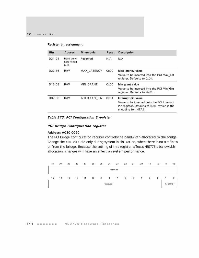
PC I bu s a r b i t e r
4 4 4 NS9775 Ha r dwa r e Re f e r ence
Register bit assignment
PCI Bridge Configuration register
Address: A030 0020The PCI Bridge Configuration register controls the bandwidth allocated to the bridge. Change the AHBBRST field only during system initialization, when there is no traffic to or from the bridge. Because the setting of this register affects NS9775’s bandwidth allocation, changes will have an effect on system performance.
Bits Access Mnemonic Reset Description
D31:24 Read only; hard-wired to 0
Reserved N/A N/A
D23:16 R/W MAX_LATENCY 0x00 Max latency valueValue to be inserted into the PCI Max_Lat register. Defaults to 0x00.
D15:08 R/W MIN_GRANT 0x00 Min grant valueValue to be inserted into the PCI Min_Gnt register. Defaults to 0x00.
D07:00 R/W INTERRUPT_PIN 0x01 Interrupt pin valueValue to be inserted onto the PCI Interrupt Pin register. Defaults to 0x01, which is the encoding for INTA#.
Table 273: PCI Configuration 3 register
Reserved
13 12 11 10 9 8 7 6 5 4 3 2 1 015 14
31 29 28 27 26 25 24 23 22 21 20 19 18 17 1630
AHBBRSTReserved
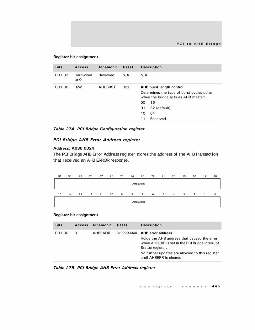
www.d i g i . com 445
PC I - t o -AHB B r i d ge
Register bit assignment
PCI Bridge AHB Error Address register
Address: A030 0024The PCI Bridge AHB Error Address register stores the address of the AHB transaction that received an AHB ERROR response.
Register bit assignment
Bits Access Mnemonic Reset Description
D31:02 Hardwired to 0
Reserved N/A N/A
D01:00 R/W AHBBRST 0x1 AHB burst length controlDetermines the type of burst cycles done when the bridge acts as AHB master:00 1601 32 (default)10 6411 Reserved
Table 274: PCI Bridge Configuration register
Bits Access Mnemonic Reset Description
D31:00 R AHBEADR 0x00000000 AHB error addressHolds the AHB address that caused the error, when AHBERR is set in the PCI Bridge Interrupt Status register.No further updates are allowed to this register until AHBERR is cleared,
Table 275: PCI Bridge AHB Error Address register
AHBEADR
13 12 11 10 9 8 7 6 5 4 3 2 1 015 14
31 29 28 27 26 25 24 23 22 21 20 19 18 17 1630
AHBEADR
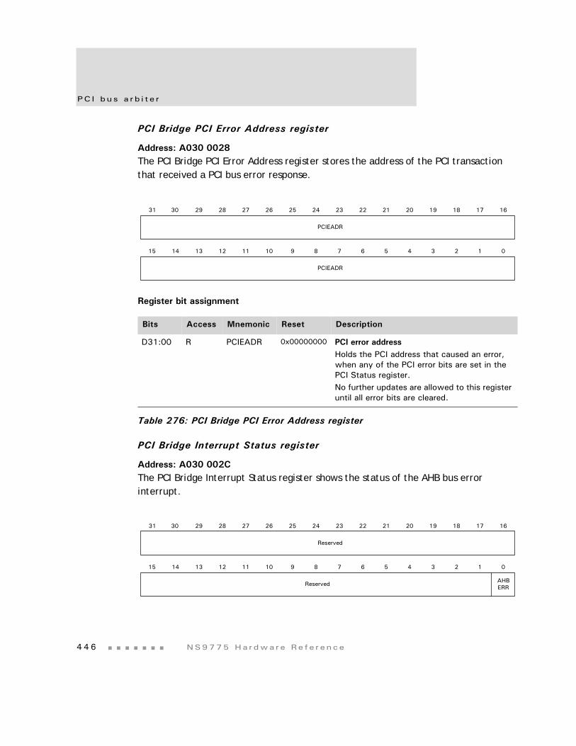
PC I bu s a r b i t e r
4 4 6 NS9775 Ha r dwa r e Re f e r ence
PCI Bridge PCI Error Address register
Address: A030 0028The PCI Bridge PCI Error Address register stores the address of the PCI transaction that received a PCI bus error response.
Register bit assignment
PCI Bridge Interrupt Status register
Address: A030 002CThe PCI Bridge Interrupt Status register shows the status of the AHB bus error interrupt.
Bits Access Mnemonic Reset Description
D31:00 R PCIEADR 0x00000000 PCI error addressHolds the PCI address that caused an error, when any of the PCI error bits are set in the PCI Status register. No further updates are allowed to this register until all error bits are cleared.
Table 276: PCI Bridge PCI Error Address register
PCIEADR
13 12 11 10 9 8 7 6 5 4 3 2 1 015 14
31 29 28 27 26 25 24 23 22 21 20 19 18 17 1630
PCIEADR
Reserved
13 12 11 10 9 8 7 6 5 4 3 2 1 015 14
31 29 28 27 26 25 24 23 22 21 20 19 18 17 1630
Reserved AHBERR
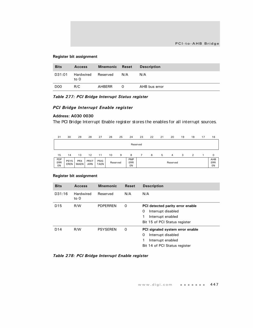
www.d i g i . com 447
PC I - t o -AHB B r i d ge
Register bit assignment
PCI Bridge Interrupt Enable register
Address: A030 0030The PCI Bridge Interrupt Enable register stores the enables for all interrupt sources.
Register bit assignment
Bits Access Mnemonic Reset Description
D31:01 Hardwired to 0
Reserved N/A N/A
D00 R/C AHBERR 0 AHB bus error
Table 277: PCI Bridge Interrupt Status register
Bits Access Mnemonic Reset Description
D31:16 Hardwired to 0
Reserved N/A N/A
D15 R/W PDPERREN 0 PCI detected parity error enable0 Interrupt disabled1 Interrupt enabledBit 15 of PCI Status register
D14 R/W PSYSEREN 0 PCI signaled system error enable0 Interrupt disabled1 Interrupt enabledBit 14 of PCI Status register
Table 278: PCI Bridge Interrupt Enable register
Reserved
AHBERREN
13 12 11 10 9 8 7 6 5 4 3 2 1 015 14
31 29 28 27 26 25 24 23 22 21 20 19 18 17 1630
ReservedReservedPDPERREN
PSYSEREN
PRXMAEN
PRXTARN
PSIGTAEN
PMPERREN
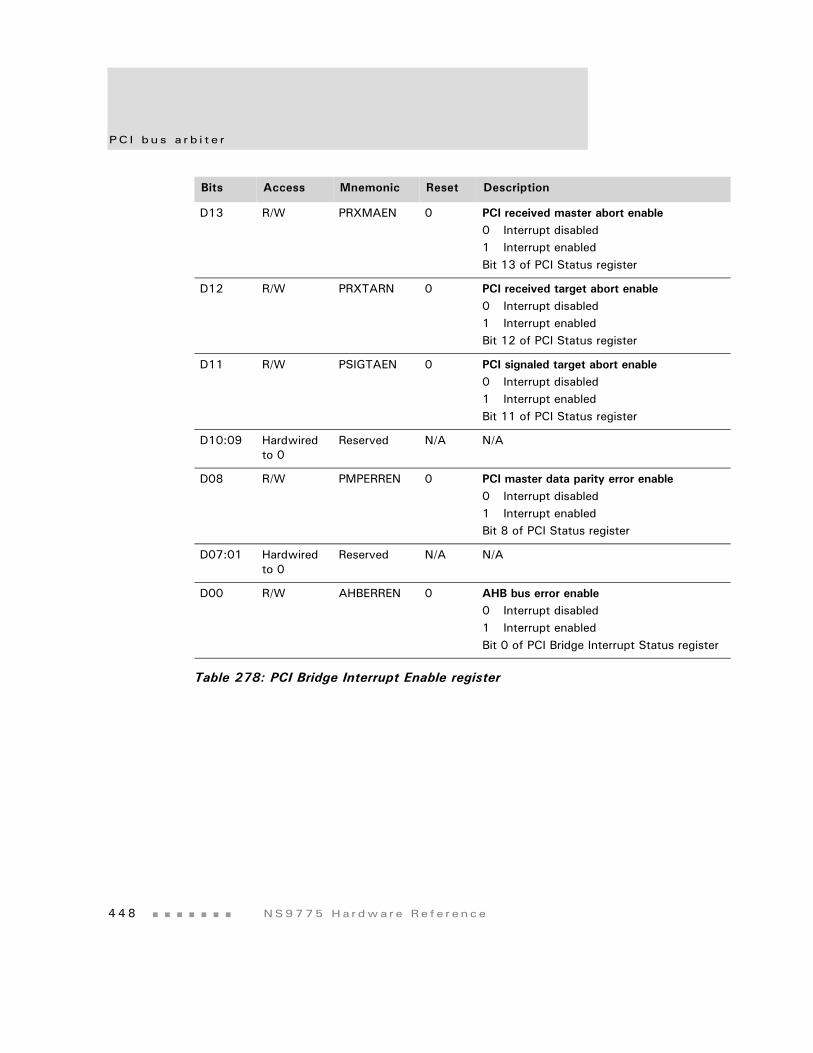
PC I bu s a r b i t e r
4 4 8 NS9775 Ha r dwa r e Re f e r ence
D13 R/W PRXMAEN 0 PCI received master abort enable0 Interrupt disabled1 Interrupt enabledBit 13 of PCI Status register
D12 R/W PRXTARN 0 PCI received target abort enable0 Interrupt disabled1 Interrupt enabledBit 12 of PCI Status register
D11 R/W PSIGTAEN 0 PCI signaled target abort enable0 Interrupt disabled1 Interrupt enabledBit 11 of PCI Status register
D10:09 Hardwired to 0
Reserved N/A N/A
D08 R/W PMPERREN 0 PCI master data parity error enable0 Interrupt disabled1 Interrupt enabledBit 8 of PCI Status register
D07:01 Hardwired to 0
Reserved N/A N/A
D00 R/W AHBERREN 0 AHB bus error enable0 Interrupt disabled1 Interrupt enabledBit 0 of PCI Bridge Interrupt Status register
Bits Access Mnemonic Reset Description
Table 278: PCI Bridge Interrupt Enable register
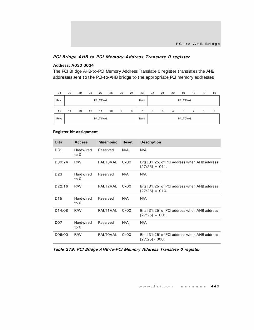
www.d i g i . com 449
PC I - t o -AHB B r i d ge
PCI Bridge AHB to PCI Memory Address Translate 0 register
Address: A030 0034The PCI Bridge AHB-to-PCI Memory Address Translate 0 register translates the AHB addresses sent to the PCI-to-AHB bridge to the appropriate PCI memory addresses.
Register bit assignment
Bits Access Mnemonic Reset Description
D31 Hardwired to 0
Reserved N/A N/A
D30:24 R/W PALT3VAL 0x00 Bits [31:25] of PCI address when AHB address [27:25] = 011.
D23 Hardwired to 0
Reserved N/A N/A
D22:16 R/W PALT2VAL 0x00 Bits [31:25] of PCI address when AHB address [27:25] = 010.
D15 Hardwired to 0
Reserved N/A N/A
D14:08 R/W PALT1VAL 0x00 Bits [31:25] of PCI address when AHB address [27:25] = 001.
D07 Hardwired to 0
Reserved N/A N/A
D06:00 R/W PALT0VAL 0x00 Bits [31:25] of PCI address when AHB address [27:25] - 000.
Table 279: PCI Bridge AHB-to-PCI Memory Address Translate 0 register
Rsvd
13 12 11 10 9 8 7 6 5 4 3 2 1 015 14
31 29 28 27 26 25 24 23 22 21 20 19 18 17 1630
PALT3VAL Rsvd
Rsvd Rsvd
PALT2VAL
PALT1VAL PALT0VAL
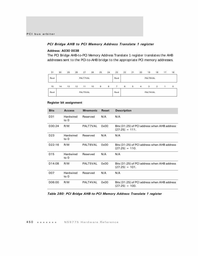
PC I bu s a r b i t e r
4 5 0 NS9775 Ha r dwa r e Re f e r ence
PCI Bridge AHB to PCI Memory Address Translate 1 register
Address: A030 0038The PCI Bridge AHB-to-PCI Memory Address Translate 1 register translates the AHB addresses sent to the PCI-to-AHB bridge to the appropriate PCI memory addresses.
Register bit assignment
Bits Access Mnemonic Reset Description
D31 Hardwired to 0
Reserved N/A N/A
D30:24 R/W PALT7VAL 0x00 Bits [31:25] of PCI address when AHB address [27:25] = 111.
D23 Hardwired to 0
Reserved N/A N/A
D22:16 R/W PALT6VAL 0x00 Bits [31:25] of PCI address when AHB address [27:25] = 110.
D15 Hardwired to 0
Reserved N/A N/A
D14:08 R/W PALT5VAL 0x00 Bits [31:25] of PCI address when AHB address [27:25] = 101.
D07 Hardwired to 0
Reserved N/A N/A
D06:00 R/W PALT4VAL 0x00 Bits [31:25] of PCI address when AHB address [27:25] = 100.
Table 280: PCI Bridge AHB-to-PCI Memory Address Translate 1 register
Rsvd
13 12 11 10 9 8 7 6 5 4 3 2 1 015 14
31 29 28 27 26 25 24 23 22 21 20 19 18 17 1630
PALT7VAL Rsvd
Rsvd Rsvd
PALT6VAL
PALT5VAL PALT4VAL
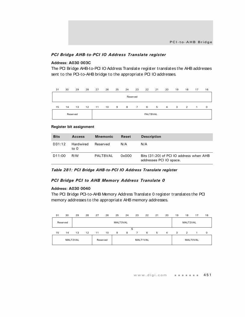
www.d i g i . com 451
PC I - t o -AHB B r i d ge
PCI Bridge AHB-to-PCI IO Address Translate register
Address: A030 003CThe PCI Bridge AHB-to-PCI IO Address Translate register translates the AHB addresses sent to the PCI-to-AHB bridge to the appropriate PCI IO addresses.
Register bit assignment
PCI Bridge PCI to AHB Memory Address Translate 0
Address: A030 0040The PCI Bridge PCI-to-AHB Memory Address Translate 0 register translates the PCI memory addresses to the appropriate AHB memory addresses.
Bits Access Mnemonic Reset Description
D31:12 Hardwired to 0
Reserved N/A N/A
D11:00 R/W PALT8VAL 0x000 Bits [31:20] of PCI IO address when AHB addresses PCI IO space.
Table 281: PCI Bridge AHB-to-PCI IO Address Translate register
Reserved
13 12 11 10 9 8 7 6 5 4 3 2 1 015 14
31 29 28 27 26 25 24 23 22 21 20 19 18 17 1630
PALT8VALReserved
Reserved
13 12 11 10 9 8 7 6 5 4 3 2 1 015 14
31 29 28 27 26 25 24 23 22 21 20 19 18 17 1630
MALT3VAL MALT2VAL
MALT1VAL MALT0VALMALT2VAL Reserved
s
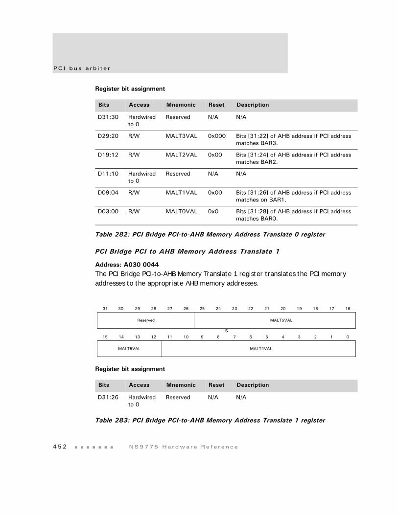
PC I bu s a r b i t e r
4 5 2 NS9775 Ha r dwa r e Re f e r ence
Register bit assignment
PCI Bridge PCI to AHB Memory Address Translate 1
Address: A030 0044The PCI Bridge PCI-to-AHB Memory Translate 1 register translates the PCI memory addresses to the appropriate AHB memory addresses.
Register bit assignment
Bits Access Mnemonic Reset Description
D31:30 Hardwired to 0
Reserved N/A N/A
D29:20 R/W MALT3VAL 0x000 Bits [31:22] of AHB address if PCI address matches BAR3.
D19:12 R/W MALT2VAL 0x00 Bits [31:24] of AHB address if PCI address matches BAR2.
D11:10 Hardwired to 0
Reserved N/A N/A
D09:04 R/W MALT1VAL 0x00 Bits [31:26] of AHB address if PCI address matches on BAR1.
D03:00 R/W MALT0VAL 0x0 Bits [31:28] of AHB address if PCI address matches BAR0.
Table 282: PCI Bridge PCI-to-AHB Memory Address Translate 0 register
Bits Access Mnemonic Reset Description
D31:26 Hardwired to 0
Reserved N/A N/A
Table 283: PCI Bridge PCI-to-AHB Memory Address Translate 1 register
Reserved
13 12 11 10 9 8 7 6 5 4 3 2 1 015 14
31 29 28 27 26 25 24 23 22 21 20 19 18 17 1630
MALT5VAL
MALT4VALMALT5VAL
s
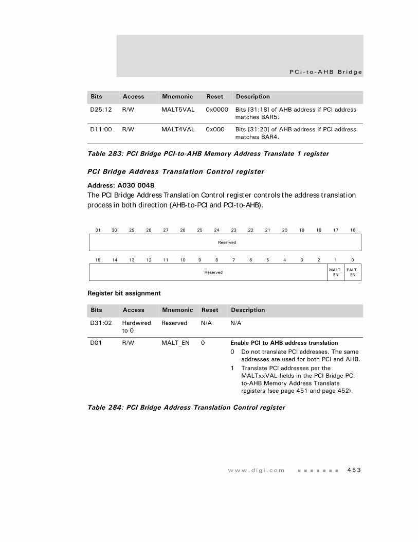
www.d i g i . com 453
PC I - t o -AHB B r i d ge
PCI Bridge Address Translation Control register
Address: A030 0048The PCI Bridge Address Translation Control register controls the address translation process in both direction (AHB-to-PCI and PCI-to-AHB).
Register bit assignment
D25:12 R/W MALT5VAL 0x0000 Bits [31:18] of AHB address if PCI address matches BAR5.
D11:00 R/W MALT4VAL 0x000 Bits [31:20] of AHB address if PCI address matches BAR4.
Bits Access Mnemonic Reset Description
D31:02 Hardwired to 0
Reserved N/A N/A
D01 R/W MALT_EN 0 Enable PCI to AHB address translation0 Do not translate PCI addresses. The same
addresses are used for both PCI and AHB.1 Translate PCI addresses per the
MALTxxVAL fields in the PCI Bridge PCI-to-AHB Memory Address Translate registers (see page 451 and page 452).
Table 284: PCI Bridge Address Translation Control register
Bits Access Mnemonic Reset Description
Table 283: PCI Bridge PCI-to-AHB Memory Address Translate 1 register
Reserved
13 12 11 10 9 8 7 6 5 4 3 2 1 015 14
31 29 28 27 26 25 24 23 22 21 20 19 18 17 1630
Reserved MALT_EN
PALT_EN
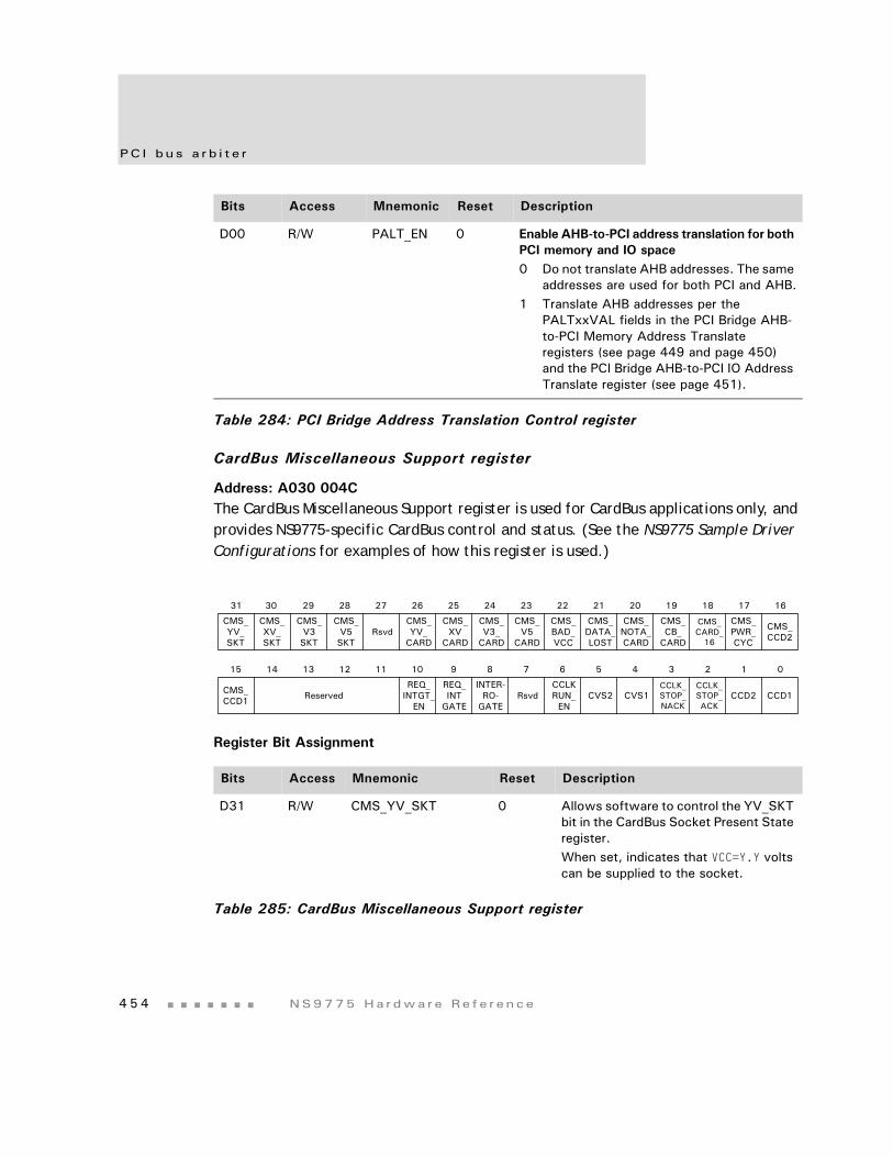
PC I bu s a r b i t e r
4 5 4 NS9775 Ha r dwa r e Re f e r ence
CardBus Miscellaneous Support register
Address: A030 004CThe CardBus Miscellaneous Support register is used for CardBus applications only, and provides NS9775-specific CardBus control and status. (See the NS9775 Sample Driver Configurations for examples of how this register is used.)
Register Bit Assignment
D00 R/W PALT_EN 0 Enable AHB-to-PCI address translation for both PCI memory and IO space0 Do not translate AHB addresses. The same
addresses are used for both PCI and AHB.1 Translate AHB addresses per the
PALTxxVAL fields in the PCI Bridge AHB-to-PCI Memory Address Translate registers (see page 449 and page 450) and the PCI Bridge AHB-to-PCI IO Address Translate register (see page 451).
Bits Access Mnemonic Reset Description
D31 R/W CMS_YV_SKT 0 Allows software to control the YV_SKT bit in the CardBus Socket Present State register.When set, indicates that VCC=Y.Y volts can be supplied to the socket.
Table 285: CardBus Miscellaneous Support register
Bits Access Mnemonic Reset Description
Table 284: PCI Bridge Address Translation Control register
REQ_INTGT_
ENReserved
REQ_INT
GATE
INTER-RO-
GATERsvd
CCLKRUN_EN
CVS2 CVS1CCLK_STOP_NACK
CCLK_STOP_ACK
CCD2 CCD1
13 12 11 10 9 8 7 6 5 4 3 2 1 015 14
CMS_CCD1
31 29 28 27 26 25 24 23 22 21 20 19 18 17 1630
CMS_V3SKT
CMS_V5SKT
CMS_YV_
CARDRsvd
CMS_XV
CARD
CMS_V3_
CARD
CMS_V5
CARD
CMS_BAD_VCC
CMS_DATA_LOST
CMS_NOTA_CARD
CMS_CB_
CARD
CMS_CARD_
16
CMS_PWR_CYC
CMS_CCD2
CMS_YV_SKT
CMS_XV_SKT
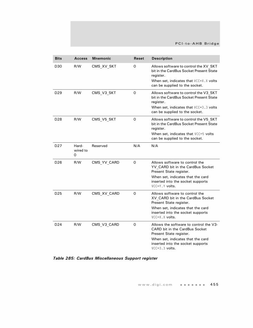
www.d i g i . com 455
PC I - t o -AHB B r i d ge
D30 R/W CMS_XV_SKT 0 Allows software to control the XV_SKT bit in the CardBus Socket Present State register.When set, indicates that VCC=X.X volts can be supplied to the socket.
D29 R/W CMS_V3_SKT 0 Allows software to control the V3_SKT bit in the CardBus Socket Present State register.When set, indicates that VCC=3.3 volts can be supplied to the socket.
D28 R/W CMS_V5_SKT 0 Allows software to control the V5_SKT bit in the CardBus Socket Present State register.When set, indicates that VCC=5 volts can be supplied to the socket.
D27 Hard-wired to 0
Reserved N/A N/A
D26 R/W CMS_YV_CARD 0 Allows software to control the YV_CARD bit in the CardBus Socket Present State register.When set, indicates that the card inserted into the socket supports VCC=Y.Y volts.
D25 R/W CMS_XV_CARD 0 Allows software to control the XV_CARD bit in the CardBus Socket Present State register.When set, indicates that the card inserted into the socket supports VCC=X.X volts.
D24 R/W CMS_V3_CARD 0 Allows the software to control the V3-CARD bit in the CardBus Socket Present State register.When set, indicates that the card inserted into the socket supports VCC=3.3 volts.
Bits Access Mnemonic Reset Description
Table 285: CardBus Miscellaneous Support register
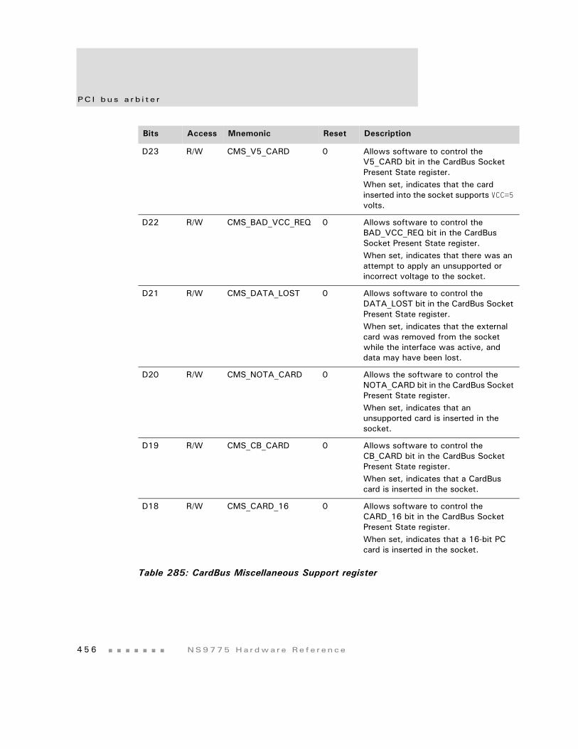
PC I bu s a r b i t e r
4 5 6 NS9775 Ha r dwa r e Re f e r ence
D23 R/W CMS_V5_CARD 0 Allows software to control the V5_CARD bit in the CardBus Socket Present State register.When set, indicates that the card inserted into the socket supports VCC=5 volts.
D22 R/W CMS_BAD_VCC_REQ 0 Allows software to control the BAD_VCC_REQ bit in the CardBus Socket Present State register.When set, indicates that there was an attempt to apply an unsupported or incorrect voltage to the socket.
D21 R/W CMS_DATA_LOST 0 Allows software to control the DATA_LOST bit in the CardBus Socket Present State register. When set, indicates that the external card was removed from the socket while the interface was active, and data may have been lost.
D20 R/W CMS_NOTA_CARD 0 Allows the software to control the NOTA_CARD bit in the CardBus Socket Present State register.When set, indicates that an unsupported card is inserted in the socket.
D19 R/W CMS_CB_CARD 0 Allows software to control the CB_CARD bit in the CardBus Socket Present State register. When set, indicates that a CardBus card is inserted in the socket.
D18 R/W CMS_CARD_16 0 Allows software to control the CARD_16 bit in the CardBus Socket Present State register.When set, indicates that a 16-bit PC card is inserted in the socket.
Bits Access Mnemonic Reset Description
Table 285: CardBus Miscellaneous Support register
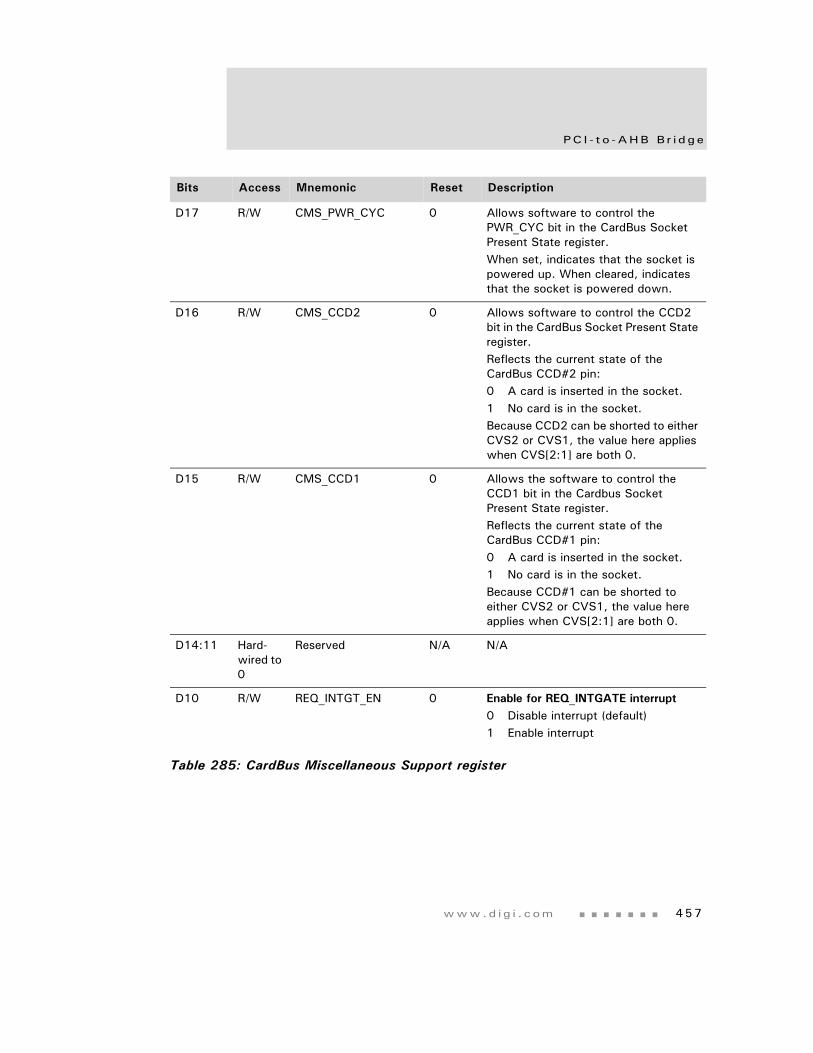
www.d i g i . com 457
PC I - t o -AHB B r i d ge
D17 R/W CMS_PWR_CYC 0 Allows software to control the PWR_CYC bit in the CardBus Socket Present State register.When set, indicates that the socket is powered up. When cleared, indicates that the socket is powered down.
D16 R/W CMS_CCD2 0 Allows software to control the CCD2 bit in the CardBus Socket Present State register.Reflects the current state of the CardBus CCD#2 pin:0 A card is inserted in the socket.1 No card is in the socket.Because CCD2 can be shorted to either CVS2 or CVS1, the value here applies when CVS[2:1] are both 0.
D15 R/W CMS_CCD1 0 Allows the software to control the CCD1 bit in the Cardbus Socket Present State register. Reflects the current state of the CardBus CCD#1 pin:0 A card is inserted in the socket.1 No card is in the socket.Because CCD#1 can be shorted to either CVS2 or CVS1, the value here applies when CVS[2:1] are both 0.
D14:11 Hard-wired to 0
Reserved N/A N/A
D10 R/W REQ_INTGT_EN 0 Enable for REQ_INTGATE interrupt0 Disable interrupt (default)1 Enable interrupt
Bits Access Mnemonic Reset Description
Table 285: CardBus Miscellaneous Support register
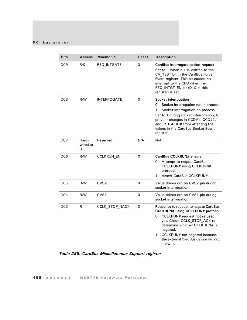
PC I bu s a r b i t e r
4 5 8 NS9775 Ha r dwa r e Re f e r ence
D09 R/C REQ_INTGATE 0 CardBus interrogate socket requestSet to 1 when a 1 is written to the CV_TEST bit in the CardBus Force Event register. This bit causes an interrupt to the CPU when the REQ_INTGT_EN bit (D10 in this register) is set.
D08 R/W INTERROGATE 0 Socket interrogation0 Socket interrogation not in process 1 Socket interrogation on processSet to 1 during socket interrogation, to prevent changes in CCD#1, CCD#2, and CSTSCHG# from affecting the values in the CardBus Socket Event register.
D07 Hard-wired to 0
Reserved N/A N/A
D06 R/W CCLKRUN_EN 0 CardBus CCLKRUN# enable0 Attempt to negate CardBus
CCLKRUN# using CCLKRUN# protocol
1 Assert CardBus CCLKRUN#
D05 R/W CVS2 0 Value driven out on CVS2 pin during socket interrogation.
D04 R/W CVS1 0 Value driven out on CVS1 pin during socket interrogation.
D03 R CCLK_STOP_NACK 0 Response to request to negate CardBus CCLKRUN# using CCLKRUN# protocol0 CCLKRUN# request not refused
yet. Check CCLK_STOP_ACK to determine whether CCLKRUN# is negated.
1 CCLKRUN# not negated because the external CardBus device will not allow it.
Bits Access Mnemonic Reset Description
Table 285: CardBus Miscellaneous Support register
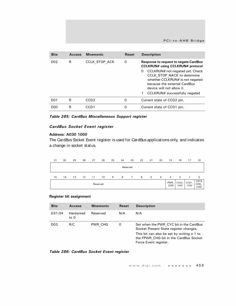
www.d i g i . com 459
PC I - t o -AHB B r i d ge
CardBus Socket Event register
Address: A030 1000The CardBus Socket Event register is used for CardBus applications only, and indicates a change in socket status.
Register bit assignment
D02 R CCLK_STOP_ACK 0 Response to request to negate CardBus CCLKRUN# using CCLKRUN# protocol0 CCLKRUN# not negated yet. Check
CCLK_STOP_NACK to determine whether CCLKRUN# is not negated because the external CardBus device will not allow it.
1 CCLKRUN# successfully negated
D01 R CCD2 0 Current state of CCD2 pin.
D00 R CCD1 0 Current state of CCD1 pin.
Bits Access Mnemonic Reset Description
D31:04 Hardwired to 0
Reserved N/A N/A
D03 R/C PWR_CHG 0 Set when the PWR_CYC bit in the CardBus Socket Present State register changes. This bit can also be set by writing a 1 to the FPWR_CHG bit in the CardBus Socket Force Event register.
Table 286: CardBus Socket Event register
Bits Access Mnemonic Reset Description
Table 285: CardBus Miscellaneous Support register
Reserved
PWR_CHG
CSTSCHG_CHG
13 12 11 10 9 8 7 6 5 4 3 2 1 015 14
31 29 28 27 26 25 24 23 22 21 20 19 18 17 1630
Reserved CCD2_CHG
CCD1_CHG
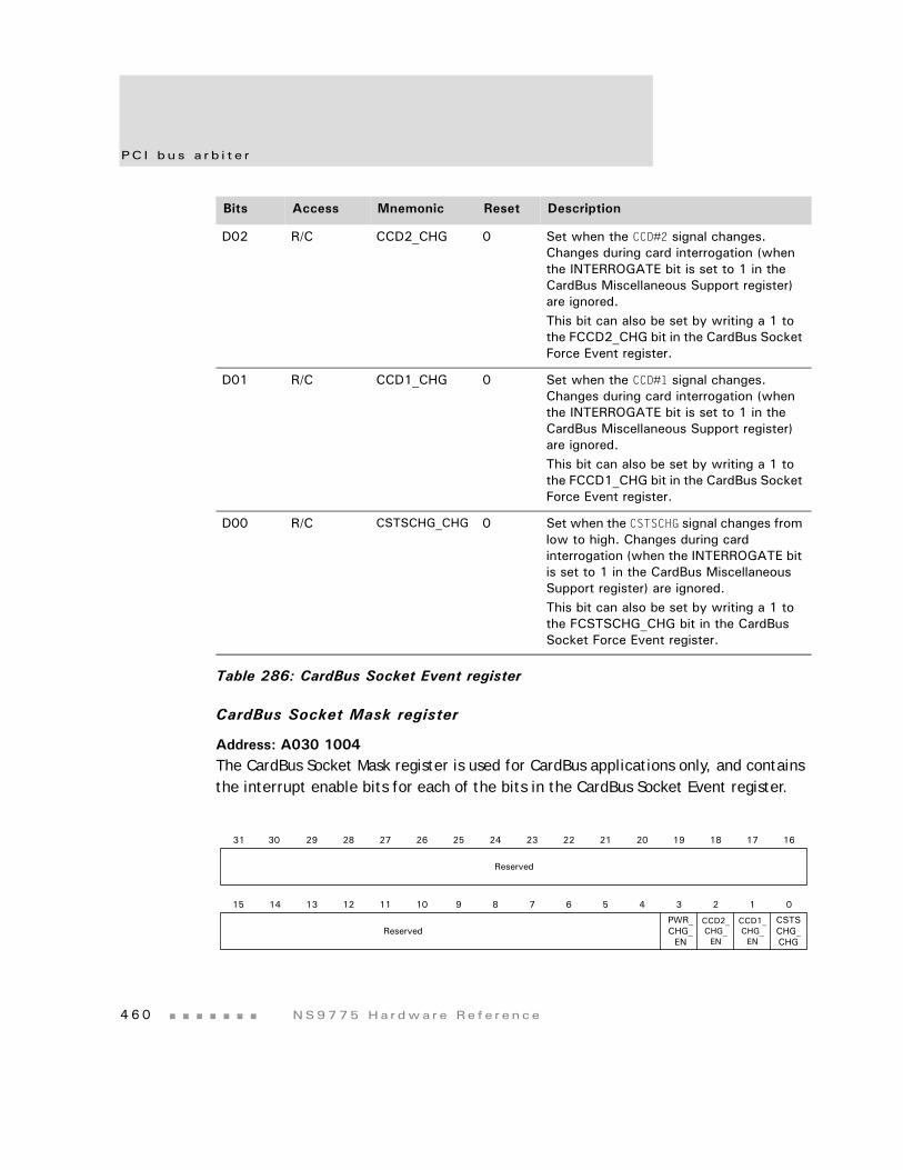
PC I bu s a r b i t e r
4 6 0 NS9775 Ha r dwa r e Re f e r ence
CardBus Socket Mask register
Address: A030 1004The CardBus Socket Mask register is used for CardBus applications only, and contains the interrupt enable bits for each of the bits in the CardBus Socket Event register.
D02 R/C CCD2_CHG 0 Set when the CCD#2 signal changes. Changes during card interrogation (when the INTERROGATE bit is set to 1 in the CardBus Miscellaneous Support register) are ignored.This bit can also be set by writing a 1 to the FCCD2_CHG bit in the CardBus Socket Force Event register.
D01 R/C CCD1_CHG 0 Set when the CCD#1 signal changes. Changes during card interrogation (when the INTERROGATE bit is set to 1 in the CardBus Miscellaneous Support register) are ignored. This bit can also be set by writing a 1 to the FCCD1_CHG bit in the CardBus Socket Force Event register.
D00 R/C CSTSCHG_CHG 0 Set when the CSTSCHG signal changes from low to high. Changes during card interrogation (when the INTERROGATE bit is set to 1 in the CardBus Miscellaneous Support register) are ignored. This bit can also be set by writing a 1 to the FCSTSCHG_CHG bit in the CardBus Socket Force Event register.
Bits Access Mnemonic Reset Description
Table 286: CardBus Socket Event register
Reserved
PWR_CHG_
EN
CSTSCHG_CHG
13 12 11 10 9 8 7 6 5 4 3 2 1 015 14
31 29 28 27 26 25 24 23 22 21 20 19 18 17 1630
ReservedCCD2_CHG_
EN
CCD1_CHG_
EN
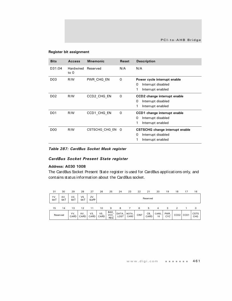
www.d i g i . com 461
PC I - t o -AHB B r i d ge
Register bit assignment
CardBus Socket Present State register
Address: A030 1008The CardBus Socket Present State register is used for CardBus applications only, and contains status information about the CardBus socket.
Bits Access Mnemonic Reset Description
D31:04 Hardwired to 0
Reserved N/A N/A
D03 R/W PWR_CHG_EN 0 Power cycle interrupt enable0 Interrupt disabled1 Interrupt enabled
D02 R/W CCD2_CHG_EN 0 CCD2 change interrupt enable0 Interrupt disabled1 Interrupt enabled
D01 R/W CCD1_CHG_EN 0 CCD1 change interrupt enable0 Interrupt disabled 1 Interrupt enabled
D00 R/W CSTSCHG_CHG_EN 0 CSTSCHG change interrupt enable0 Interrupt disabled1 Interrupt enabled
Table 287: CardBus Socket Mask register
ReservedBAD_VCC_REQ
DATA_LOST
NOTA_CARD CINT CB_
CARDCARD_
16PWR_CYC CCD2 CCD1 CSTS
CHG
13 12 11 10 9 8 7 6 5 4 3 2 1 015 14
31 29 28 27 26 25 24 23 22 21 20 19 18 17 1630
V3_SKT
V5_SKT
ZV_SUPP
YV_SKT
XV_SKT Reserved
YV_CARD
XV_CARD
V3_CARD
V5_CARD
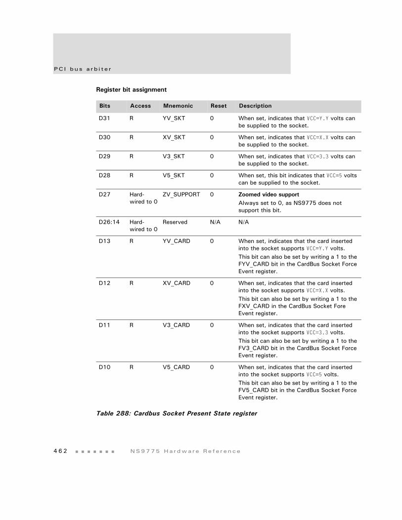
PC I bu s a r b i t e r
4 6 2 NS9775 Ha r dwa r e Re f e r ence
Register bit assignment
Bits Access Mnemonic Reset Description
D31 R YV_SKT 0 When set, indicates that VCC=Y.Y volts can be supplied to the socket.
D30 R XV_SKT 0 When set, indicates that VCC=X.X volts can be supplied to the socket.
D29 R V3_SKT 0 When set, indicates that VCC=3.3 volts can be supplied to the socket.
D28 R V5_SKT 0 When set, this bit indicates that VCC=5 volts can be supplied to the socket.
D27 Hard-wired to 0
ZV_SUPPORT 0 Zoomed video supportAlways set to 0, as NS9775 does not support this bit.
D26:14 Hard-wired to 0
Reserved N/A N/A
D13 R YV_CARD 0 When set, indicates that the card inserted into the socket supports VCC=Y.Y volts. This bit can also be set by writing a 1 to the FYV_CARD bit in the CardBus Socket Force Event register.
D12 R XV_CARD 0 When set, indicates that the card inserted into the socket supports VCC=X.X volts.This bit can also be set by writing a 1 to the FXV_CARD in the CardBus Socket Fore Event register.
D11 R V3_CARD 0 When set, indicates that the card inserted into the socket supports VCC=3.3 volts.This bit can also be set by writing a 1 to the FV3_CARD bit in the CardBus Socket Force Event register.
D10 R V5_CARD 0 When set, indicates that the card inserted into the socket supports VCC=5 volts.This bit can also be set by writing a 1 to the FV5_CARD bit in the CardBus Socket Force Event register.
Table 288: Cardbus Socket Present State register
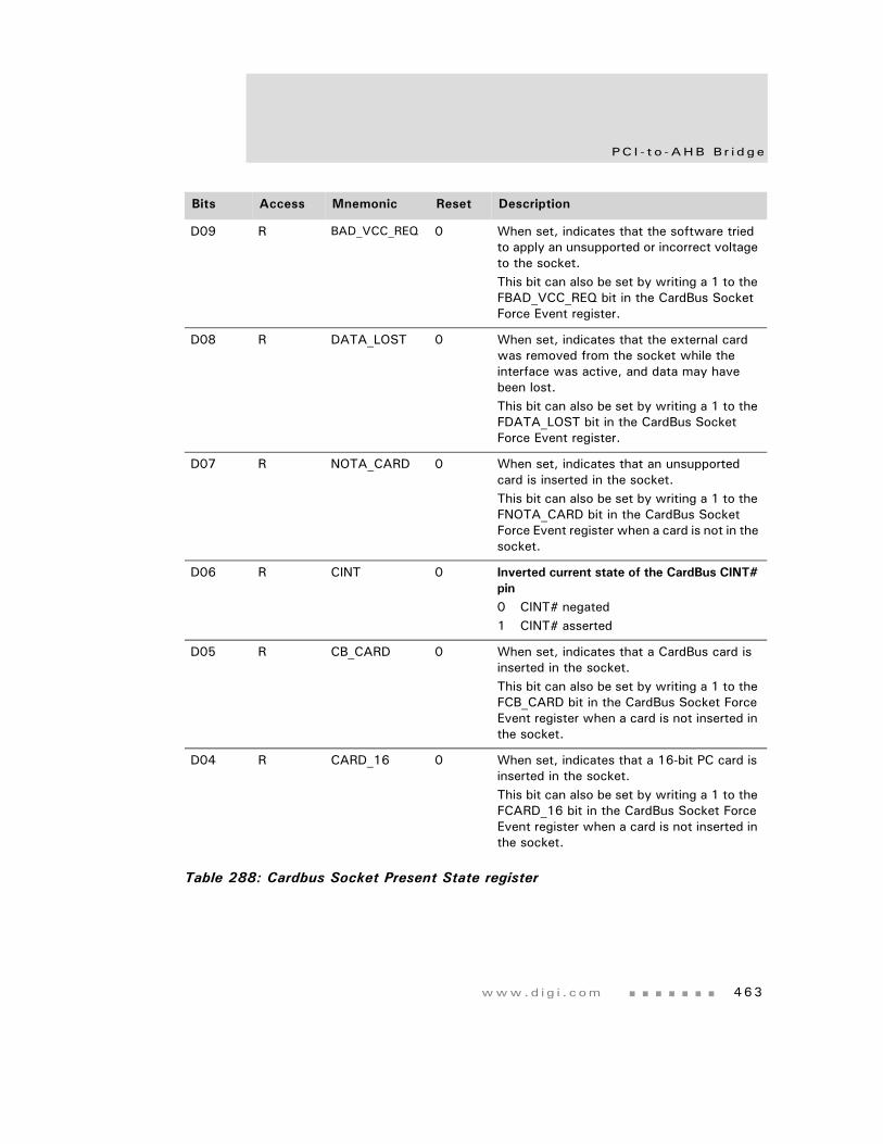
www.d i g i . com 463
PC I - t o -AHB B r i d ge
D09 R BAD_VCC_REQ 0 When set, indicates that the software tried to apply an unsupported or incorrect voltage to the socket. This bit can also be set by writing a 1 to the FBAD_VCC_REQ bit in the CardBus Socket Force Event register.
D08 R DATA_LOST 0 When set, indicates that the external card was removed from the socket while the interface was active, and data may have been lost. This bit can also be set by writing a 1 to the FDATA_LOST bit in the CardBus Socket Force Event register.
D07 R NOTA_CARD 0 When set, indicates that an unsupported card is inserted in the socket. This bit can also be set by writing a 1 to the FNOTA_CARD bit in the CardBus Socket Force Event register when a card is not in the socket.
D06 R CINT 0 Inverted current state of the CardBus CINT# pin0 CINT# negated1 CINT# asserted
D05 R CB_CARD 0 When set, indicates that a CardBus card is inserted in the socket. This bit can also be set by writing a 1 to the FCB_CARD bit in the CardBus Socket Force Event register when a card is not inserted in the socket.
D04 R CARD_16 0 When set, indicates that a 16-bit PC card is inserted in the socket.This bit can also be set by writing a 1 to the FCARD_16 bit in the CardBus Socket Force Event register when a card is not inserted in the socket.
Bits Access Mnemonic Reset Description
Table 288: Cardbus Socket Present State register
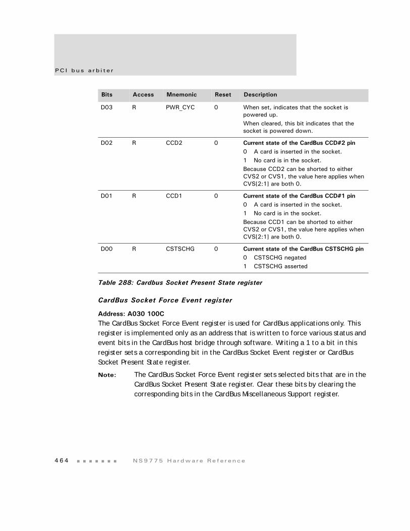
PC I bu s a r b i t e r
4 6 4 NS9775 Ha r dwa r e Re f e r ence
CardBus Socket Force Event register
Address: A030 100CThe CardBus Socket Force Event register is used for CardBus applications only. This register is implemented only as an address that is written to force various status and event bits in the CardBus host bridge through software. Writing a 1 to a bit in this register sets a corresponding bit in the CardBus Socket Event register or CardBus Socket Present State register.
Note: The CardBus Socket Force Event register sets selected bits that are in the CardBus Socket Present State register. Clear these bits by clearing the corresponding bits in the CardBus Miscellaneous Support register.
D03 R PWR_CYC 0 When set, indicates that the socket is powered up. When cleared, this bit indicates that the socket is powered down.
D02 R CCD2 0 Current state of the CardBus CCD#2 pin0 A card is inserted in the socket.1 No card is in the socket.Because CCD2 can be shorted to either CVS2 or CVS1, the value here applies when CVS[2:1] are both 0.
D01 R CCD1 0 Current state of the CardBus CCD#1 pin0 A card is inserted in the socket.1 No card is in the socket.Because CCD1 can be shorted to either CVS2 or CVS1, the value here applies when CVS[2:1] are both 0.
D00 R CSTSCHG 0 Current state of the CardBus CSTSCHG pin0 CSTSCHG negated1 CSTSCHG asserted
Bits Access Mnemonic Reset Description
Table 288: Cardbus Socket Present State register
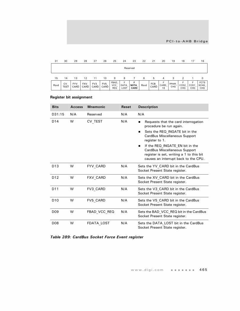
www.d i g i . com 465
PC I - t o -AHB B r i d ge
Register bit assignment
Bits Access Mnemonic Reset Description
D31:15 N/A Reserved N/A N/A
D14 W CV_TEST N/A Requests that the card interrogation procedure be run again.
Sets the REQ_INGATE bit in the CardBus Miscellaneous Support register to 1.
If the REQ_INGATE_EN bit in the CardBus Miscellaneous Support register is set, writing a 1 to this bit causes an interrupt back to the CPU.
D13 W FYV_CARD N/A Sets the YV_CARD bit in the CardBus Socket Present State register.
D12 W FXV_CARD N/A Sets the XV_CARD bit in the CardBus Socket Present State register.
D11 W FV3_CARD N/A Sets the V3_CARD bit in the CardBus Socket Present State register.
D10 W FV5_CARD N/A Sets the V5_CARD bit in the CardBus Socket Present State register.
D09 W FBAD_VCC_REQ N/A Sets the BAD_VCC_REQ bit in the CardBus Socket Present State register.
D08 W FDATA_LOST N/A Sets the DATA_LOST bit in the CardBus Socket Present State register.
Table 289: CardBus Socket Force Event register
Reserved
FCTSSCHG_CHG
13 12 11 10 9 8 7 6 5 4 3 2 1 015 14
31 29 28 27 26 25 24 23 22 21 20 19 18 17 1630
Rsvd CV_TEST
FV3_CARD
FBAD_VCC_REQ
FNOTA_CARD
FDATA_LOST
FV5_CARD Rsvd FCB_
CARD
FCARD_
16
FPWR_CHG
FCCD2_CHG
FCCD1_CHG
FYV_CARD
FXV_CARD
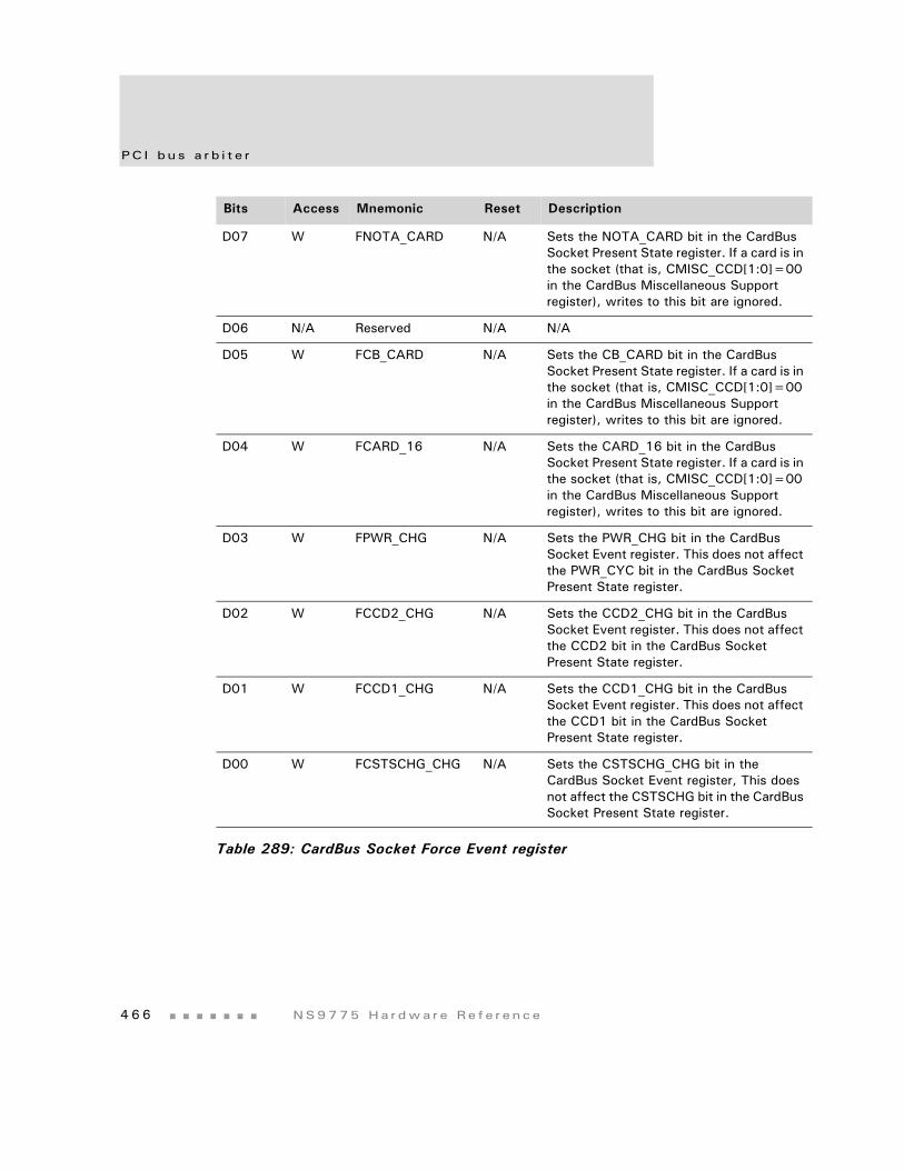
PC I bu s a r b i t e r
4 6 6 NS9775 Ha r dwa r e Re f e r ence
D07 W FNOTA_CARD N/A Sets the NOTA_CARD bit in the CardBus Socket Present State register. If a card is in the socket (that is, CMISC_CCD[1:0]=00 in the CardBus Miscellaneous Support register), writes to this bit are ignored.
D06 N/A Reserved N/A N/A
D05 W FCB_CARD N/A Sets the CB_CARD bit in the CardBus Socket Present State register. If a card is in the socket (that is, CMISC_CCD[1:0]=00 in the CardBus Miscellaneous Support register), writes to this bit are ignored.
D04 W FCARD_16 N/A Sets the CARD_16 bit in the CardBus Socket Present State register. If a card is in the socket (that is, CMISC_CCD[1:0]=00 in the CardBus Miscellaneous Support register), writes to this bit are ignored.
D03 W FPWR_CHG N/A Sets the PWR_CHG bit in the CardBus Socket Event register. This does not affect the PWR_CYC bit in the CardBus Socket Present State register.
D02 W FCCD2_CHG N/A Sets the CCD2_CHG bit in the CardBus Socket Event register. This does not affect the CCD2 bit in the CardBus Socket Present State register.
D01 W FCCD1_CHG N/A Sets the CCD1_CHG bit in the CardBus Socket Event register. This does not affect the CCD1 bit in the CardBus Socket Present State register.
D00 W FCSTSCHG_CHG N/A Sets the CSTSCHG_CHG bit in the CardBus Socket Event register, This does not affect the CSTSCHG bit in the CardBus Socket Present State register.
Bits Access Mnemonic Reset Description
Table 289: CardBus Socket Force Event register
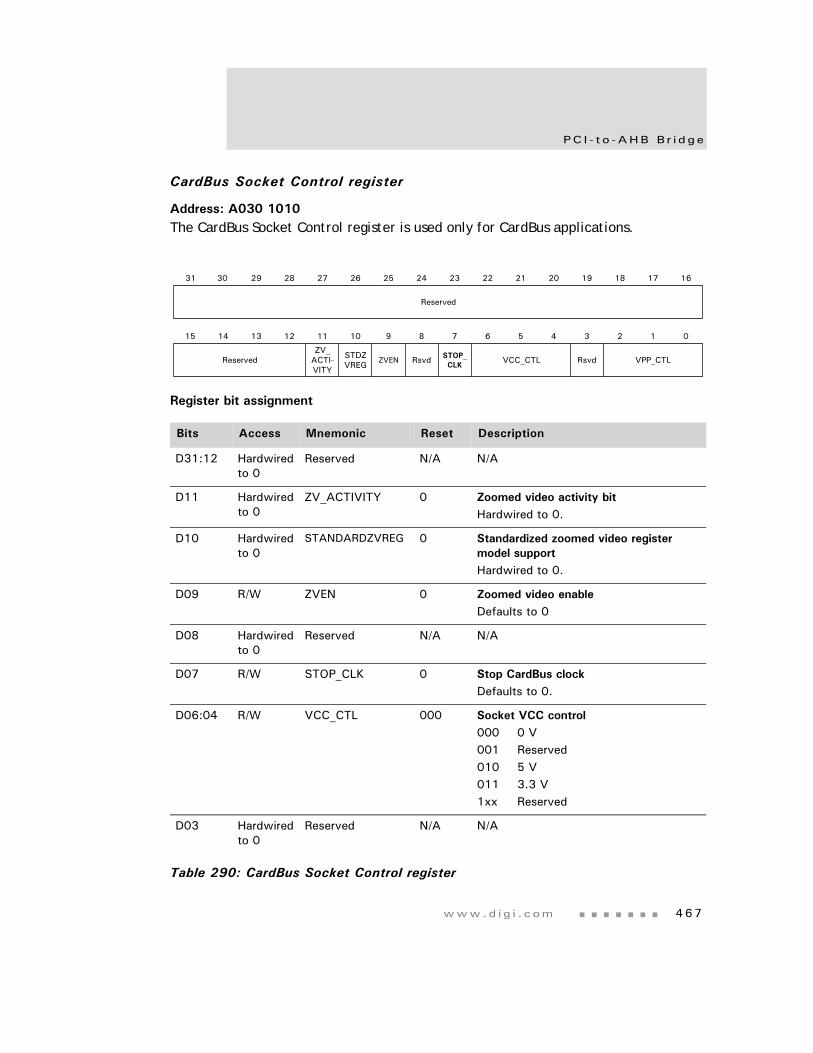
www.d i g i . com 467
PC I - t o -AHB B r i d ge
CardBus Socket Control register
Address: A030 1010The CardBus Socket Control register is used only for CardBus applications.
Register bit assignment
Bits Access Mnemonic Reset Description
D31:12 Hardwired to 0
Reserved N/A N/A
D11 Hardwired to 0
ZV_ACTIVITY 0 Zoomed video activity bitHardwired to 0.
D10 Hardwired to 0
STANDARDZVREG 0 Standardized zoomed video register model supportHardwired to 0.
D09 R/W ZVEN 0 Zoomed video enableDefaults to 0
D08 Hardwired to 0
Reserved N/A N/A
D07 R/W STOP_CLK 0 Stop CardBus clockDefaults to 0.
D06:04 R/W VCC_CTL 000 Socket VCC control000 0 V001 Reserved010 5 V011 3.3 V1xx Reserved
D03 Hardwired to 0
Reserved N/A N/A
Table 290: CardBus Socket Control register
Reserved
13 12 11 10 9 8 7 6 5 4 3 2 1 015 14
31 29 28 27 26 25 24 23 22 21 20 19 18 17 1630
ZV_ACTI-VITY
Reserved ZVEN STOP_CLK
RsvdSTDZVREG VCC_CTL Rsvd VPP_CTL
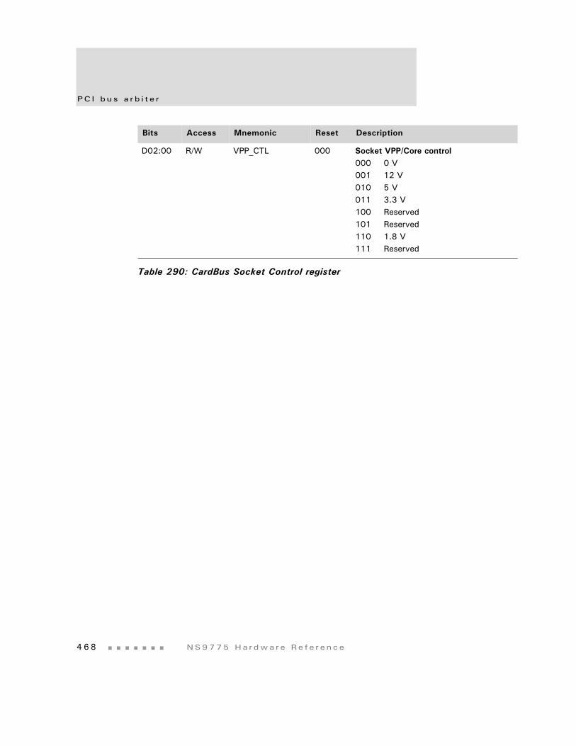
PC I bu s a r b i t e r
4 6 8 NS9775 Ha r dwa r e Re f e r ence
D02:00 R/W VPP_CTL 000 Socket VPP/Core control000 0 V001 12 V010 5 V011 3.3 V100 Reserved101 Reserved110 1.8 V111 Reserved
Bits Access Mnemonic Reset Description
Table 290: CardBus Socket Control register
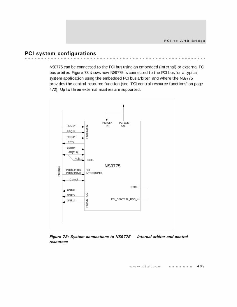
www.d i g i . com 469
PC I - t o -AHB B r i d ge
PCI system configurations
NS9775 can be connected to the PCI bus using an embedded (internal) or external PCI bus arbiter. Figure 73 shows how NS9775 is connected to the PCI bus for a typical system application using the embedded PCI bus arbiter, and where the NS9775 provides the central resource function (see "PCI central resource functions" on page 472). Up to three external masters are supported.
Figure 73: System connections to NS9775 — Internal arbiter and central resources
NS9775
REQ1#
REQ2#
REQ3#
GNT3#
GNT2#
GNT1#
PC
I RE
Q IN
PC
I GN
T O
UT
AD[31:0]
PC
I BU
S
Control
AD[11] IDSEL
INTB#,INTC#,INTD#,INTA#
PCIINTERRUPTS
PCI CLKOUT
PCI CLKIN
SERR#
RST#
PCI_CENTRAL_RSC_n1
RTCK1
PC I s y s t em con f i g u r a t i o n s
4 7 0 NS9775 Ha r dwa r e Re f e r ence
Note:1 These pins are not connected because internal resistors tie these pins to the appropriate
state.
The internal PCI arbiter is selected when the RTCK pin is set to 1 during powerup. Because the RTCK pad has a weak internal pullup, no external components are required to select the internal PCI arbiter.
Figure 74 shows how NS9775 is connected to the PCI bus for a typical application using an external PCI bus arbiter, and where the NS9775 does not provide the PCI central resource functions (see "PCI central resource functions" on page 472). RTCK is pulled low by an external resistor to configure NS9775 to use an external arbiter. The REQ0#/GNT0# pair for the external PCI arbiter is multiplexed out on the GNT1#/REQ1# pins — GNT1# to REQ0# and REQ1# to GNT0#.
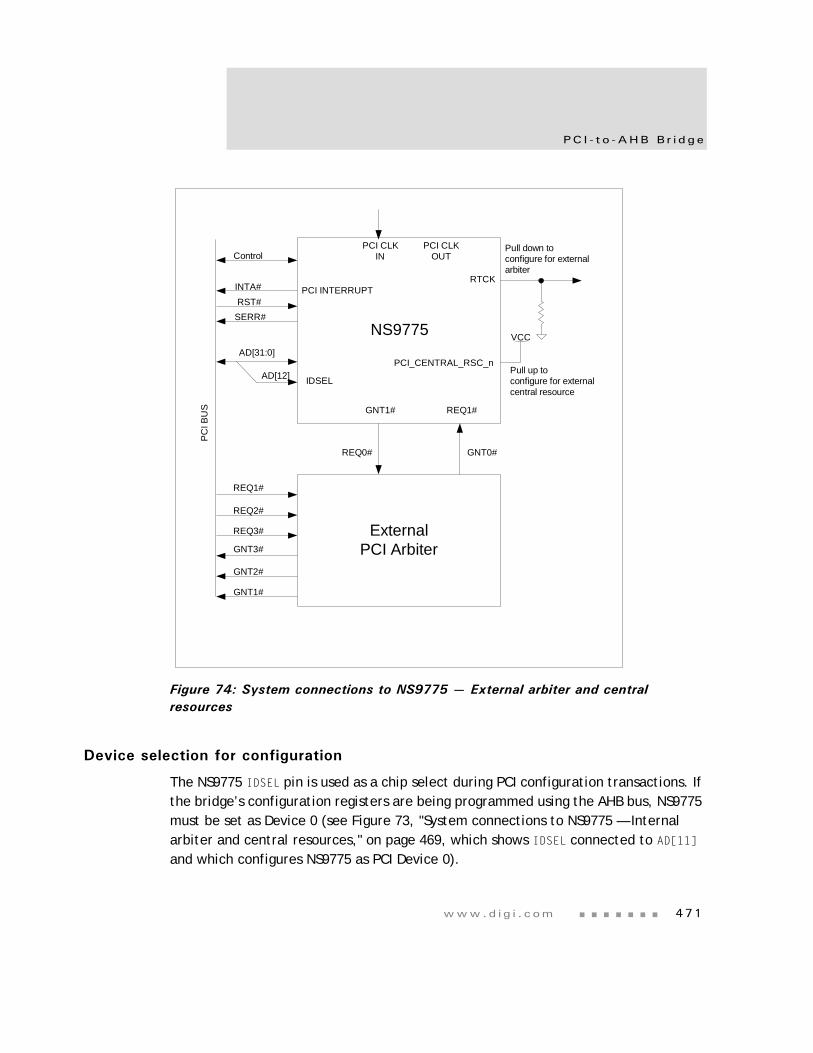
www.d i g i . com 471
PC I - t o -AHB B r i d ge
Figure 74: System connections to NS9775 — External arbiter and central resources
Device selection for configuration
The NS9775 IDSEL pin is used as a chip select during PCI configuration transactions. If the bridge’s configuration registers are being programmed using the AHB bus, NS9775 must be set as Device 0 (see Figure 73, "System connections to NS9775 — Internal arbiter and central resources," on page 469, which shows IDSEL connected to AD[11] and which configures NS9775 as PCI Device 0).
NS9775
REQ1#
REQ2#
REQ3#
GNT3#
GNT2#
GNT1#
AD[31:0]
PC
I BU
S
Control
AD[12] IDSEL
PCI INTERRUPTINTA#
PCI CLKOUT
PCI CLKIN
ExternalPCI Arbiter
REQ0# GNT0#
GNT1# REQ1#
RTCK
Pull down toconfigure for externalarbiter
PCI_CENTRAL_RSC_n
VCC
RST#SERR#
Pull up toconfigure for externalcentral resource
PC I s y s t em con f i g u r a t i o n s
4 7 2 NS9775 Ha r dwa r e Re f e r ence
If the bridge’s configuration registers are programmed using an external PCI device, NS9775 can be configured as any PCI device number (see Figure 74, "System connections to NS9775 — External arbiter and central resources," on page 471, which shows IDSEL connected to AD[12] and which configured NS9775 as Device 1). Any accesses from the AHB bus to the bridge’s configuration registers, however, must be done as Device 0.
PCI interrupts
NS9775 can serve as the interrupt controller for all four PCI interrupts. These interrupts go directly to the interrupt controller in the System Control module. Because these interrupts are open-drain type signals, the transition from low to high is relatively slow once the source of the interrupt is cleared. SERR# input can also cause an interrupt through PCISERR (in the PCI Arbiter Interrupt Status register).
Important: The system software must provide adequate time for the interrupt signals and SERR# to rise before re-enabling them.
If an external interrupt controller is used, NS9775 can drive INTA# using INTA2PCI (in the PCI Miscellaneous Support register).
PCI central resource functions
NS9775 provides several PCI central resource functions when NS9775’s PCI_CENTRAL_RSC_n pin is pulled low (see Figure 73):
RST# to the PCI system is driven through NS9775. RST# is asserted asynchronously and negated synchronously to the PCI clock. RST# is driven from the system reset to NS9775 and the PCI bit in the Reset and Sleep Control register in the System Control Module.
SERR# is configured as an input.
AD[31:0], C/BE[3:0], and PAR are driven low when RST# is asserted, to keep the signals from floating.
www.d i g i . com 473
PC I - t o -AHB B r i d ge
When the PCI_CENTRAL_RSC_n pin is pulled high (see Figure 74), these functions operate differently:
RST# is configured as an input, and must be supplied by the system. In this situation, RST# is used as another system reset to NS9775; that is, either reset_n or RST# can reset NS9775, and both must be negated to take NS9775 out of reset.
SERR# is configured as output.
AD[31:0], C/BE[3:0], and PAR are tri-stated when RST# is asserted.
The system must provide pullup resistors on the following signals, regardless of the state of PCI_CENTRAL_RSC_n:
FRAME#
TRDY#
IRDY#
DEVSEL#
STOP#
SERR#
PERR#
LOCK#
Note: The NS9775 does not have a LOCK# pin associated with it. If any PCI device in the system uses the LOCK# signal, the signal must have a pullup resistor.
INTA#
INTB#
INTC#
INTD#
All REQ# inputs to NS9775
All GNT# outputs from NS9775 that are connected to other PCI devices in the system (because they are tri-stated during RST#)
The PCI clock can be either generated from NS9775 (see Figure 73, "System connections to NS9775 — Internal arbiter and central resources," on page 469) or provided by an external source (see Figure 74, "System connections to NS9775 — External arbiter and central resources," on page 471). The PCI CLK input pad has a weak internal pullup.
Ca rdBus Suppo r t
4 7 4 NS9775 Ha r dwa r e Re f e r ence
Important: Note that in cases where NS9775 provides the PCI clock, the PCI clock connection to the NS9775 must still be made external to the NS9775, as shown in Figure 74 (that is, connect PCI_clk_out to PCI_clk_in). This is done to minimize the clock skew between the NS9775 and external PCI devices.
CardBus Support
NS9775 can support 32-bit CardBus applications using the existing PCI port and existing PCI-to-AHB bridge IP.
Figure 75 shows how NS9775 is configured for CardBus applications. The CardBus model has only one external card connected to a host adapter or PCI-to-CardBus bridge through a socket. All connections are point-to-point, and both the host adapter and the external card can be masters on the bus.
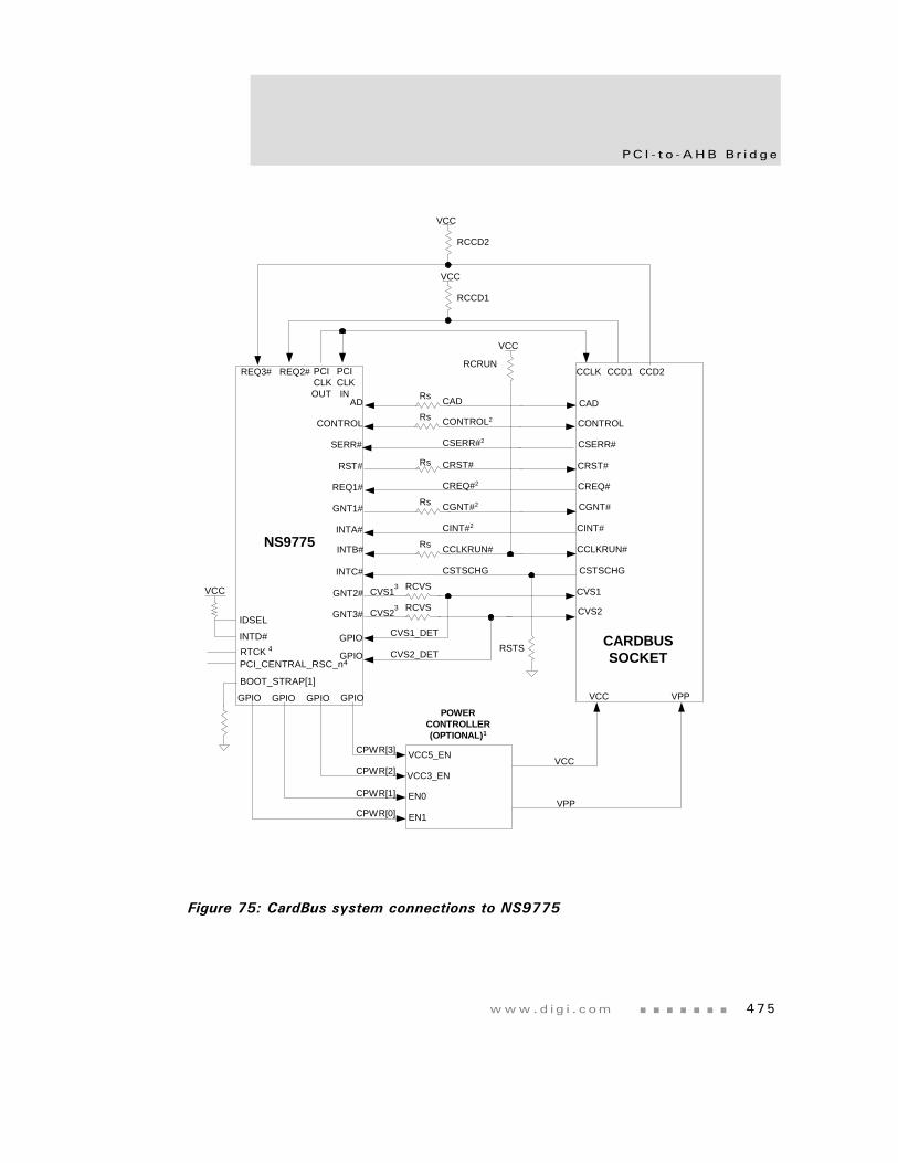
www.d i g i . com 475
PC I - t o -AHB B r i d ge
Figure 75: CardBus system connections to NS9775
CONTROL
NS9775
PCI_CENTRAL_RSC_n
PCI CLK
IN
PCI CLKOUT
REQ2#REQ3#
VCC
CCD2CCD1
AD
SERR#
RST#
REQ1#
GNT1#
INTA#
INTB#
INTC#
GNT2#
GNT3#
CONTROL
CAD
CSERR#
CRST#
CREQ#
CINT#
CVS1
CGNT#
CCLKRUN#
CSTSCHG
CVS2
CAD
CONTROL2
CSERR#2
CRST#
CREQ#2
CGNT#2
CINT#2
CCLKRUN#
CSTSCHG
GPIO
GPIO
BOOT_STRAP[1]
IDSEL
VCC
GPIO GPIO GPIO GPIO
VCC5_EN
VCC3_EN
EN0
EN1
VCC VPP
VCC
VPP
POWERCONTROLLER(OPTIONAL)1
CARDBUSSOCKET
CCLK
RCCD1
RCVS
RCVS
VCC
RCCD2
CVS1_DET
CVS2_DET
CPWR[3]
CPWR[2]
CPWR[1]
CPWR[0]
Rs
Rs
Rs
Rs
Rs
VCC
RSTS
RCRUN
CVS1
CVS2
3
3
4RTCKINTD#
4
Ca rdBus Suppo r t
4 7 6 NS9775 Ha r dwa r e Re f e r ence
Notes:1 The power controller is required only for applications that support hot-insertion
and hot-removal of the CardBus card. This requires additional components to isolate NS9775 from CardBus.
2 The system must provide external pullup per PCI specification. CAD, C/BE, and PAR do not require pullups.
3 Voltage detection signal optional for embedded system.
4 Pins not connected because internal resistors tie these to the appropriate state.
Configuring NS9775 for CardBus support
Although many CardBus signals are the same as those for the PCI bus, there are some unique signals. Table 291 lists the new signals and indicates the PCI signals with which they are multiplexed for NS9775.
PCI SignalCardBus Signal CardBus type Comments
INTA# CINT# Input Cardbus interrupt pin. INTA2PCI in the PCI Miscellaneous Support register must be 0.
INTB# CCLKRUN# Bidir CardBus pin used to negotiate with the external CardBus device before stopping the clock. Also allows external CardBus device to request that the clock be restarted.
INTC# CSTSCHG Input CardBus status change interrupt signal.
GNT1# CGNT# Output Grant to external CardBus device from NS9775’s internal arbiter.
GNT2# CVS1 Output Voltage sense pin. Normally driven low by NS9775, but toggled during interrogation of external CardBus device to detect voltage requirements.
GNT3# CVS2 Output Voltage sense pin. Normally driven low by NS9775 but toggled during interrogation of external CardBus device to detect voltage requirements.
REQ1# CREQ# Input Request from external CardBus device to NS9775’s internal arbiter.
Table 291: CardBus IO muxing
www.d i g i . com 477
PC I - t o -AHB B r i d ge
Notes:BP_STAT_OUT[0] and PCI_CENTRAL_RSC_n are two strapping pins that must be pulled low to configure the IO and internal arbiter for CardBus. Because CardBus does not have an IDSEL signal, it is pulled high. As a result, NS9775 captures any configuration accesses from the external CardBus device since it is the only other device on the bus.
The internal arbiter must be used for CardBus applications. Requests to the arbiter from the REQ2# and REQ3# pins, however, must be disabled by clearing the PCIEN_M2 and PCIEN_M3 bits in the PCI Arbiter Configuration register. The arbiter parks the bus only on the bridge — not on the last granted master, as is done for PC I.
REQ2# CCD1 Input Card detect pin. Pulled up by system when socket is empty and pulled low when the external CardBus device is present in the socket.
REQ3# CCD2 Input Card detect pin. Pulled up by system when socket is empty and pulled low when the external CardBus device is present in the socket.
N/A CVS1_DET Input Voltage sense detect pin. Can be any GPIO input. Used to detect whether the external CardBus device shorts CVS1 to ground.
N/A CVS2_DET Input Voltage sense detect pin. Can be any GPIO input. Used to detect whether the external device shorts CVS2 to ground.
N/A CPWR[3:0] Output Controls to the external power controller that may be providing the power to the CardBus socket. Required only for hot-insertion and hot-removal. Can be any GPIO outputs.
PCI SignalCardBus Signal CardBus type Comments
Table 291: CardBus IO muxing
Ca rdBus Suppo r t
4 7 8 NS9775 Ha r dwa r e Re f e r ence
CardBus adapter requirements
In a CardBus application, NS9775 is the adapter, or bridge. The adapter is required to have a set of socket registers that provide socket control and status. The following NS9775 registers support this requirement:
CardBus Socket Event (see "CardBus Socket Event register" on page 459)
CardBus Socket Mask (see "CardBus Socket Mask register" on page 460)
CardBus Socket Present State (see "CardBus Socket Present State register" on page 461)
CardBus Socket Force Event (see "CardBus Socket Force Event register" on page 464)
CardBus Socket Control (see "CardBus Socket Control register" on page 467)
CardBus interrupts
The dedicated CINT# signal on the CardBus is connected directly to the interrupt controller in the System Control module, as Interrupt #10 (that is, the same as the INTA# signal for the PCI bus). Table 292 shows the CardBus-related maskable interrupt conditions that are reported to the System Control module’s interrupt controller through the PCI arbiter’s interrupt.
See the sections on PCI configuration and powered socket configuration, in the NS9775 Sample Driver Configurations, for information about configuring NS9775 properly for use with the CardBus.
Bit field Register
CSTSCHG_CHG CardBus Socket Event
CCD1_CHG CardBus Socket Event
CCD2_CHG CardBus Socket Event
PWR_CHG CardBus Socket Event
REQ_INTGATE CardBus Miscellaneous Support
CCLKRUN PCI Arbiter Interrupt Status
Table 292: CardBus interrupt sources
479
BBus BridgeC H A P T E R 8
The NS9775 ASIC contains two busses that interconnect the peripherals. The high speed peripherals reside on the AMBA AHB bus. The low speed peripherals reside on the Digi proprietary BBus. The main function of the BBus bridge is to connect the main AHB bus to the proprietary Digi BBus. Both bus interfaces have a master and a slave interface.
BBus b r i dg e f unc t i on s
4 8 0 NS9775 Ha r dwa r e Re f e r ence
BBus bridge functions
The Digi BBus is a low-speed secondary bus that operates at half the AHB clock frequency. The BBus interface houses the slower serial interfaces for USB, IEEE 1284, SPI, and UART, as well as dedicated BBus DMA control, to offload some of the bandwidth demands of the primary AHB bus. The BBus bridge controls the flow of data between the AHB and BBus interfaces.
The BBus bridge provides these functions:
BBus arbitration and multiplexing. The USB and DMA peripheral, in addition to the BBus bridge, can be BBus masters. All BBus peripherals contain a slave interface.
Two-channel DMA controller. The DMA controller performs memory-to-memory transfers across the AHB bus, allowing DMA transfers from an external peripheral to external memory or from external memory to an external peripheral.
System boot engine that fetches data from an external SPI-EEPROM and writes it to an external SDRAM. The boot engine configures the memory controller accordingly, before fetching the contents of the EEPROM. While a serial boot operation takes place, the CPU is held in reset.
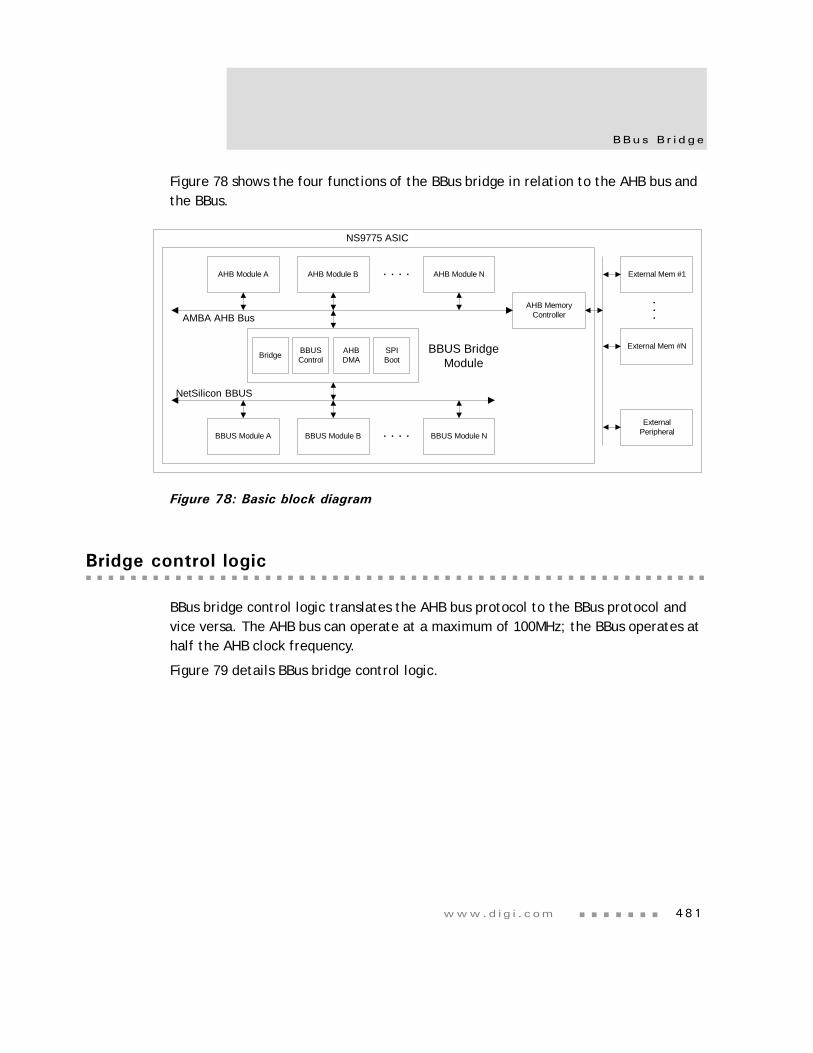
www.d i g i . com 481
BBus B r i d ge
Figure 78 shows the four functions of the BBus bridge in relation to the AHB bus and the BBus.
Figure 78: Basic block diagram
Bridge control logic
BBus bridge control logic translates the AHB bus protocol to the BBus protocol and vice versa. The AHB bus can operate at a maximum of 100MHz; the BBus operates at half the AHB clock frequency.
Figure 79 details BBus bridge control logic.
AHB Module A AHB Module NAHB Module B . . . .
BBUS Module A
AHB MemoryController
BBUS Module B BBUS Module N. . . .
AMBA AHB Bus
NetSilicon BBUS
External Mem #1
External Mem #N
ExternalPeripheral
. . .
BBUS BridgeModule
NS9775 ASIC
Bridge BBUSControl
AHBDMA
SPIBoot
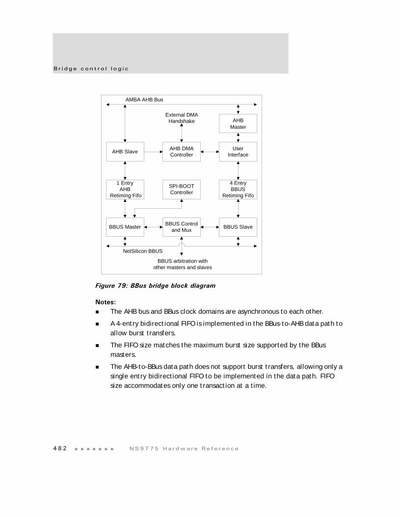
B r i dge con t r o l l o g i c
4 8 2 NS9775 Ha r dwa r e Re f e r ence
Figure 79: BBus bridge block diagram
Notes:The AHB bus and BBus clock domains are asynchronous to each other.
A 4-entry bidirectional FIFO is implemented in the BBus-to-AHB data path to allow burst transfers.
The FIFO size matches the maximum burst size supported by the BBus masters.
The AHB-to-BBus data path does not support burst transfers, allowing only a single entry bidirectional FIFO to be implemented in the data path. FIFO size accommodates only one transaction at a time.
AHB Slave
BBUS Master
1 EntryAHB
Retiming Fifo
BBUS Controland Mux BBUS Slave
4 EntryBBUS
Retiming Fifo
AMBA AHB Bus
NetSilicon BBUS
BBUS arbitration withother masters and slaves
UserInterface
AHB DMAController
External DMAHandshake
SPI-BOOTController
AHBMaster
www.d i g i . com 483
BBus B r i d ge
DMA accesses
There are two DMA controllers on the NS9775 BBus. One DMA controller services all BBus peripherals except the USB device; the other is dedicated to the USB device. Each DMA controller contains 16 channels that perform both DMA read and DMA write transactions.
Note: The USB host is a bus mastering BBus peripheral.
DMA memory-to-peripheral transfers (DMA read). DMA read transactions begin with the DMA controller arbitrating for BBus control. When the bus has been granted, the read transaction is presented to the BBus slave interface within the BBus bridge. The command then is passed into the BBus command retiming FIFO, where the user interface picks it up and passes it to the AHB master interface. The AHB master arbitrates for the AHB bus, performs the specified AHB read transaction, and returns the data to the BBus retiming data FIFO. When the BBus slave detects the data in the retiming data FIFO, the BBus slave can respond to the read request from the BBus master.
The AMBA AHB bus can indicate the burst size at the beginning of a new transfer; the AHB master sets the hburst[2:0] signals to the appropriate value. Because the BBus cannot indicate burst size, the user interface always issues a 4-transfer (4-word) request, which goes into the BBus retiming FIFO. When data is transferred to the BBus, as many words as are needed are moved. When the BBus read transaction completes, any words remaining in the retiming FIFO are flushed.
DMA peripheral-to-memory transfers (DMA write). DMA write transactions begin with the DMA controller arbitrating for control of the BBus. Once the bus is granted, the write transaction is presented to the BBus slave interface within the BBus bridge. The BBus slave interface passes the command data to the BBus data retiming FIFO, but retains the command until the BBus transaction completes. At this point, the BBus slave knows the size of the burst (by counting the number of transfers); that information is passed with the command to the BBus retiming command FIFO. When the BBus detects the presence of the command, it passes the command to the AHB master. The AHB master arbitrates for the AHB bus and performs the AHB write transaction.
BBus con t r o l l o g i c
4 8 4 NS9775 Ha r dwa r e Re f e r ence
BBus control logic
BBus control logic consists of a round-robin arbiter to select a new master, the multiplexing logic to provide the new master’s signals to the BBus slaves, and address decoding to select the target BBus slave.
BBus bridge masters and slaves
BBus bridge arbitration allows each bus master to control the bus in a round-robin manner. If a bus master does not require the bus resources when its turn comes around, that bus master is skipped until the next round-robin slot. Each potential bus master presents the bus with request and attribute signals. Once the bus grants mastership, the targeted device is selected.
Note: The CPU always is granted mastership when requested, because its transactions are time-sensitive and completed within 4 BBus clock cycles. When the CPU requests use of the bus, it must wait until the current transaction finishes. The CPU then takes mastership and performs its transaction, before the next BBus master with a pending request. When the CPU transaction is finished, the bus grants mastership to the appropriate requesting BBus master.
Table 304 shows the BBus bus master and slave modules.
Module Master Slave
BBus bridge Y Y
BBus DMA Y Y
SER Y
I2C Y
1284 Y
USB dev Y
USB DMA Y Y
USB host Y Y
Table 304: BBus master and slave modules
www.d i g i . com 485
BBus B r i d ge
Cycles and BBus arbitration
During a normal cycle, each bus master cycle is allowed only one read/write cycle if another bus master is waiting. There are two exceptions to this rule: burst transactions and read-modify-write transactions.
In a burst transaction, the master can perform more than one read or write cycle. In a read-modify-write transaction, the bus master performs one read and write cycle to the same location.
BBus peripheral address map (decoding)
The BBus address map is divided to allow access to the internal modules and external resources routed through the internal peripherals. The BBus configuration registers are located at base address 0xA040 0000 and are dedicated a 1 MB address space. The BBus peripherals are located at base address 0x9000 0000 and span a 256 MB address space. Each BBus peripheral, with the exception of the SER port controllers, resides in a separate 1 MB address space.
Table 305 specifies the address space given to each peripheral.
Base address Peripheral
0x9000 0000 BBus DMA controller
0x9010 0000 USB controller
0x9020 0000 SER Port #B
0x9020 0040 SER Port #A
0x9030 0000 SER Port #C
0x9030 0040 SER Port #D
0x9040 0000 IEEE-1284 controller
0x9050 0000 I2C controller
0x9060 0000 BBus utility
Table 305: BBus peripheral address map
Two - channe l AHB DMA con t r o l l e r (AHB bu s )
4 8 6 NS9775 Ha r dwa r e Re f e r ence
Two-channel AHB DMA controller (AHB bus)
Each DMA channel moves data from the source address to the destination address. Transfers can be specified as burst-oriented to maximize AHB bus efficiency. All transfers are executed in two steps:
1 Data is moved from the source address to an 8-entry buffer in the DMA control logic.
2 Data is moved from the 8-entry buffer to the destination address.
These steps are repeated until the DMA transfer is complete. Note that optimum performance is achieved when the source and destination addresses are word-aligned.
Initiating a DMA transfer
There are two ways to initiate a DMA transfer: processor-initiated and external-peripheral initiated.
When the processor initiates the DMA transfer, it performs these steps:
1 Sets up the required buffer descriptors.
2 Configures the appropriate DMA Channel 1/2 Control register (see "DMA Channel 1/2 Control register" on page 503).
3 Writes a 1 to the channel enable (CE) and channel go (CG) fields in the DMA Channel 1/2 Control register (see "DMA Channel 1/2 Control register" on page 503).
The external peripheral initiates a DMA transfer by asserting the appropriate REQ signal. Software must set up the required buffer descriptors and configure the DMA Channel 1/2 Control register (including setting the CE field to 1) before asserting the REQ signal.
DMA buffer descriptor
All DMA channels in NS9775 use a buffer descriptor. When a DMA channel is activated, it reads the DMA buffer descriptor pointed to by the Buffer Descriptor Pointer register (see "Buffer Descriptor Pointer register" on page 502). A DMA buffer descriptor is always fetched using an AHB INCR4 transaction, to maximize AHB bus bandwidth.
www.d i g i . com 487
BBus B r i d ge
When the current descriptor is retired, the next descriptor is accessed from a circular buffer.
Each DMA buffer descriptor requires four 32-bit words to describe a transfer. Circular buffers of 1024 bytes contain multiple buffer descriptors. The first buffer descriptor address is provided by the DMA channel’s Buffer Descriptor Pointer register. Subsequent buffer descriptors are found adjacent to the first descriptor. The final buffer descriptor is defined with its W bit set. When the DMA channel encounters the W bit, the channel wraps around to the first descriptor.
Each DMA channel can address a maximum of 64 buffer descriptors, each consisting of 16 bytes. Configuring the DMA channel for more than the maximum number of buffer descriptors results in unpredictable behavior.
Figure 80 shows the DMA buffer descriptor. Table 306 describes each section.
Figure 80: BBus bridge DMA buffer descriptor
Field/Section Description
Source address Identifies the starting location of the source data. The source address can be aligned to any byte boundary. Optimum performance results when the source address is aligned on a word boundary
Buffer length Indicates the number of bytes to move between the source and the destination. After completing the transfer, the DMA controller updates this field with the actual number of bytes moved.
Destination address Identifies the beginning of the location to which the source data will be moved. The destination address can be aligned to any byte boundary. Optimum performance results when the destination address is aligned on a word boundary.
Table 306: BBus bridge DMA buffer descriptor definition
Destination Address
Buffer Length
Status
Source AddressOFFSET + 0
OFFSET + 4
OFFSET + 8
OFFSET + C FI LW Reserved
31 30 29 28 16 15 0
Reserved
Two - channe l AHB DMA con t r o l l e r (AHB bu s )
4 8 8 NS9775 Ha r dwa r e Re f e r ence
Descriptor list processing
When a DMA controller has completed the operation specified by the current buffer descriptor, the controller clears the F bit and fetches the next buffer descriptor. A
W The wrap bit. When set, this bit tells the DMA controller that this is the last buffer descriptor within the continuous list of descriptors. The next buffer descriptor is found using the initial DMA channel buffer descriptor pointer. When the wrap bit is not set, the next buffer descriptor is found using an offset of 0x10 from the current buffer descriptor.
I The interrupt bit. Tells the DMA controller to issue an interrupt to the CPU when the buffer is closed due to normal channel completion. The interrupt occurs no matter what the normal completion interrupt enable configuration is for the DMA channel.
L The last bit. When set, this bit tells the DMA controller that this buffer descriptor is the last descriptor that completes an entire message frame. The DMA controller uses this bit to assert the normal channel completion status when the byte count reaches zero.If this bit is set, the DMA controller remains in the IDLE state after asserting the normal channel completion status. A write to the CE field in the DMA Channel 1/2 Control register re-enables the DMA channel.
F The full bit. When set, this bit indicates that the buffer descriptor is valid and can be processed by the DMA channel.
The DMA channel clears this bit after completing the transfer(s).
The DMA channel doesn’t try a transfer with the F bit clear.
The DMA channel enters an IDLE state after fetching a buffer descriptor with the F bit cleared.
When the device driver modifies the F bit, it must also write a 1 to the CE bit in the DMA Channel 1/2 Control register to activate the idle channel.
Reserved Write zero to this field.
Status Not used. Read back 0x0000.
Field/Section Description
Table 306: BBus bridge DMA buffer descriptor definition
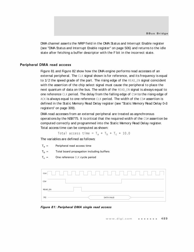
www.d i g i . com 489
BBus B r i d ge
DMA channel asserts the NRIP field in the DMA Status and Interrupt Enable register (see "DMA Status and Interrupt Enable register" on page 506) and returns to the idle state after fetching a buffer descriptor with the F bit in the incorrect state.
Peripheral DMA read access
Figure 81 and Figure 82 show how the DMA engine performs read accesses of an external peripheral. The CLK signal shown is for reference, and its frequency is equal to 1/2 the speed grade of the part. The rising edge of the READ_EN signal coincident with the assertion of the chip select signal must cause the peripheral to place the next quantum of data on the bus. The width of the READ_EN signal is always equal to one reference CLK period. The delay from the falling edge of CS# to the rising edge of ACK is always equal to one reference CLK period. The width of the CS# assertion is defined in the Static Memory Read Delay register (see "Static Memory Read Delay 0–3 registers" on page 309).
DMA read accesses from an external peripheral are treated as asynchronous operations by the NS9775. It is critical that the required width of the CS# assertion be computed correctly and programmed into the Static Memory Read Delay register. Total access time can be computed as shown:
Total access time = Ta + Tb + Tc + 10.0
The variables are defined as follows:
Figure 81: Peripheral DMA single read access
Ta = Peripheral read access time
Tb = Total board propagation including buffers
Tc = One reference CLK cycle period
DATA VALID
READ_EN
DQ
CS#
CLK
Two - channe l AHB DMA con t r o l l e r (AHB bu s )
4 9 0 NS9775 Ha r dwa r e Re f e r ence
Figure 82: Peripheral DMA burst read access
Peripheral DMA write access
Figure 83 and Figure 84 show how the DMA engine performs write accesses of an external peripheral. The clock signal shown is for reference, and its clock frequency is equal to 1/2 the speed grade of the part. Data should be written on the rising edge of the WE# signal. Data and control signals are always held after the rising edge of WE# for one reference CLK cycle. The CS# signal is guaranteed to be deasserted for at least one CLK cycle between successive peripheral write accesses. The widths of the CS# assertion and the WE# assertion are defined using the Static Memory Write Delay register and the Static Memory Write Enable Delay register in the Memory Controller (see "Static Memory Read Delay 0–3 registers" on page 309 and "Static Memory Write Enable Delay 0–3 registers" on page 307).
Note that the ACK signal is not used during peripheral DMA write accesses.
Figure 83: Peripheral DMA single write access
READ_EN
DQ
CS#
CLK
DATA0 DATA1
DQ
CS#
CLK
WE#
Data Valid
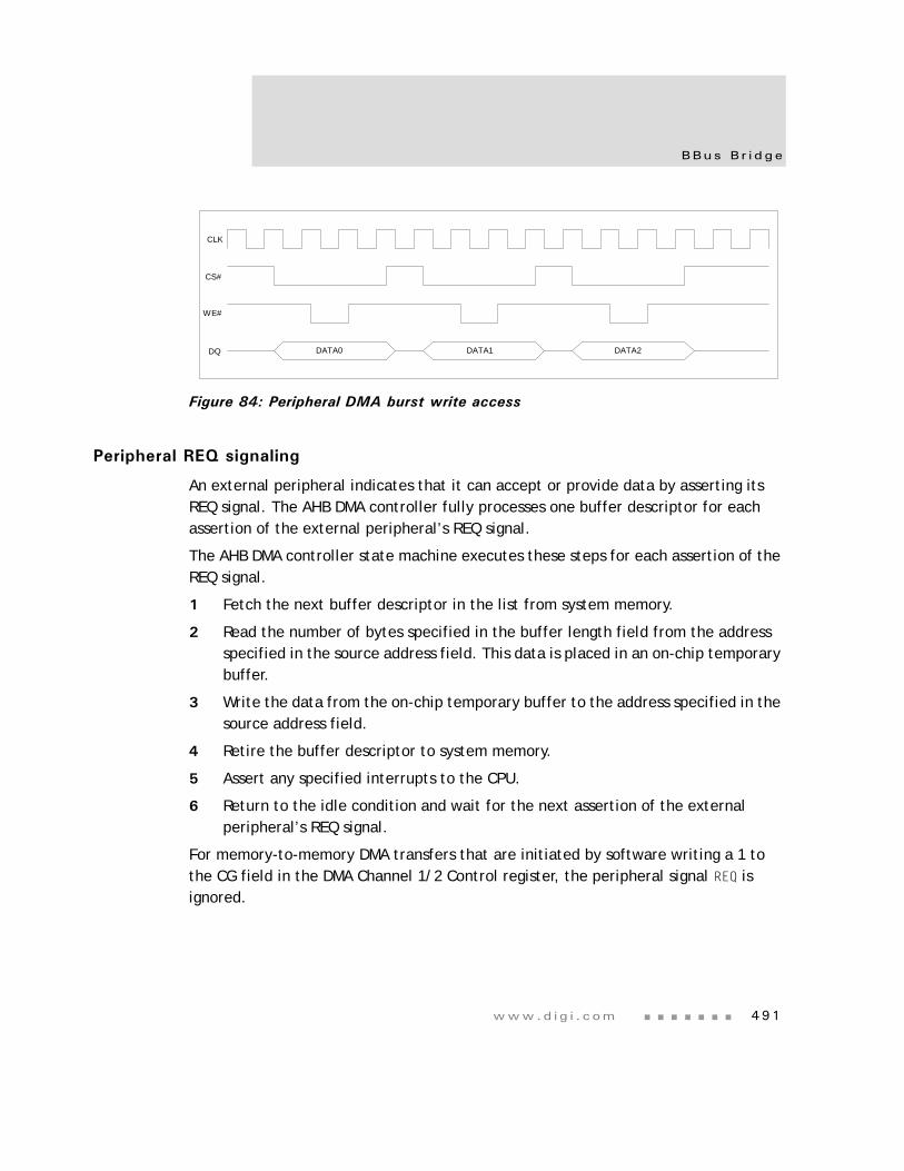
www.d i g i . com 491
BBus B r i d ge
Figure 84: Peripheral DMA burst write access
Peripheral REQ signaling
An external peripheral indicates that it can accept or provide data by asserting its REQ signal. The AHB DMA controller fully processes one buffer descriptor for each assertion of the external peripheral’s REQ signal.
The AHB DMA controller state machine executes these steps for each assertion of the REQ signal.
1 Fetch the next buffer descriptor in the list from system memory.
2 Read the number of bytes specified in the buffer length field from the address specified in the source address field. This data is placed in an on-chip temporary buffer.
3 Write the data from the on-chip temporary buffer to the address specified in the source address field.
4 Retire the buffer descriptor to system memory.
5 Assert any specified interrupts to the CPU.
6 Return to the idle condition and wait for the next assertion of the external peripheral’s REQ signal.
For memory-to-memory DMA transfers that are initiated by software writing a 1 to the CG field in the DMA Channel 1/2 Control register, the peripheral signal REQ is ignored.
CLK
DATA0 DATA1 DATA2
CS#
WE#
DQ
Two - channe l AHB DMA con t r o l l e r (AHB bu s )
4 9 2 NS9775 Ha r dwa r e Re f e r ence
Design Limitations
The AHB DMA logic contains several design limitations. Carefully consider these limitations when making system level implementation decisions:
The AHB DMA control logic is designed to operate on four-byte quantities, which limits the minimum number of accesses that the memory controller can perform on narrow external peripherals. Accesses to an 8-bit peripheral will always occur in multiples of four. Accesses to a 16-bit peripheral will always occur in multiples of two. Asserting the REQ signal when the peripheral is unable to meet the above conditions results in unpredictable system behavior.
The length field in the buffer descriptor must be set to a value equal to the burst length multiplied by four. The burst length is specified in the SB/DB field in the DMA Channel 1/2 Control register.
The peripheral can assert the REQ signal no more often than the AHB DMA response latency for the given system (see "Calculating AHB DMA response latency" on page 492).
The REQ signal is an asynchronous input to the NS9775. For a REQ signal assertion to be found by the control logic, it must be asserted for no less than 4 AHB clock cycles and no more than 20 AHB clock cycles.
The AHB DMA channels are allocated the unused BBus peripheral bandwidth, which limits the bandwidth available to the AHB DMA channels. Minimum bandwidth requirements can be met by allocating more AHB bus timeslots to the BBus master using the BRC registers in the System Control module.
The AHB DMA channels provide no latency guarantee because they do not directly attach to the AHB bus. Allocating more system bandwidth reduces the worst case latency. In a fully loaded system, the response to the REQ signal assertion can be as long as 83us.
Calculating AHB DMA response latency
AHB DMA controller latency is defined as the time between the assertion of the peripheral’s REQ signal and the AHB DMA channel being granted access to the AHB bus. Response latency is a function of the number of AHB timeslots given to the BBus and the number of BBus peripherals in use. Note that the BBus peripherals
www.d i g i . com 493
BBus B r i d ge
transferring data in non-DMA mode do not contribute to the calculation. The worst case AHB DMA response latency occurs when all of the BBus peripherals perform these operations within several microseconds of each other:
Move the remaining data in or out of the data buffer.
Close the buffer descriptor.
Open a new buffer descriptor.
Begin processing the new data buffer. This can be two steps for a transmitter.
Two AHB bandwidth calculations are defined here. The first scheme shows the worst case, where the BBus is given one out of ten AHB timeslots. The second scheme shows the best case, where the BBus is given one out of every four AHB timeslots.
Worst case:
AHB access = ((16 * 10 * 2) / 200 MHz) = 1.60usThis AHB access pattern looks like this:
Cpu, Erx, Cpu, Etx; Cpu, Lcd, Cpu, Pci; Cpu, BBusBest case:
AHB access = ((16 * 4 * 2) / 200 MHz) = 0.64usThis AHB access pattern looks like this:
Cpu, Erx, Cpu, BBus; Cpu, Etx, Cpu, BBus; Cpu, Lcd, Cpu, BBus; Cpu, Pci; Cpu, BBus
Each receive channel contributes four AHB accesses to the calculation. Each transmit channel contributes five AHB accesses to the calculation. The USB device (or USB host) and IEEE 1284 are half-duplex-only peripherals, so only the transmit channel needs to be accounted for.
Also take into account adjustment for AHB DMA channel overhead: two if one DMA channel is in use and six if both DMA channels are in use. The worst case and best case equations for two DMA channels work out as shown:
Worst case latency = 1.60us * ((#Receive * 4) + (#Transmit * 5) + 6)
Best case latency = 0.64us * ((#Receive * 4) + (#Transmit * 5) + 6)
In a fully loaded system with four UARTs, IEEE 1284, and USB, the worst case latency is 83.2us and the best case latency is 33.28us.
Two - channe l AHB DMA con t r o l l e r (AHB bu s )
4 9 4 NS9775 Ha r dwa r e Re f e r ence
Static RAM chip select configuration
The AHB DMA controller accesses an external peripheral using the external memory bus and one of the static RAM chip select signals (st_cs_n[N]). This table describes how to program the static RAM chip select control registers for access using the AHB DMA controller.
Fields not explicitly listed should be left in the reset state.
Fields listed but not defined must be defined by the user.
Register Name Field Value Comment
Configuration PB 1 System requirement.
PM user defined Set to 1 if it is not necessary for the chip select signal to toggle for each access.
MW user defined N/A
Read Delay WTRD user defined Compute the total delay using the equation provided in "Peripheral DMA read access" on page 489. The total delay should be divided by the AHB clock period to produce this value. Round up any fractional result.
Page Read Delay WTPG user defined For most applications, this value will be the same as the value for WTRD.
Output Enable Delay WOEN user defined If the ACK signal is used to initiate a peripheral read, this field should be setto 0. If signal st_oe_n is used to initiate a peripheral read, this field should be set to (at least) 1.
Write Enable Delay WWEN user defined For most applications, this field can be left in the default state.
Write Delay WTWR user defined For most applications, this field can be left in the default state.
Turn Delay WTTN user defined For most applications, this field can be left in the default state.
Table 307: Static RAM chip select configuration
www.d i g i . com 495
BBus B r i d ge
Interrupt aggregation
All the peripherals on the BBus, as well as AHB DMA channels 1 and 2 in the BBus bridge, can interrupt the CPU when attention is required. These interrupts are aggregated in the BBus bridge, and a single interrupt is presented to the System Control Module on the bbus_int signal.
This function is performed in the BBus bridge because it allows the processor to quickly identify which BBus peripheral(s) is requesting attention. (See "BBus Bridge Interrupt Status register" on page 509 for more information.)
Note: The interrupt(s) must be serviced in the peripheral in which the interrupt(s) originated.
Bandwidth requirements
A single AHB timeslot is sufficient to support the ideal maximum bandwidth of the BBus peripherals plus overhead for DMA buffer descriptors. The maximum case occurs with four SPI masters, IEEE 1284, and either USB device or USB host.
The SPI master interfaces support a maximum of 6.25 Mbps of full duplex traffic.
The IEEE-1284 interface supports a maximum of 2 Mbps of full duplex traffic.
The USB supports a maximum of 12 Mbps of full duplex traffic.
The total peripheral bandwidth is 64Mbps. Adding 8 Mbps for DMA buffer descriptors brings the total requirement to 9 MBps, less than one AHB timeslot with a full 16-slot rotation.
Important: Be aware that the AHB DMA channels and the BBus peripherals share an AHB timeslot. The BBus peripherals are always given a higher priority than the AHB DMA channels. The busier the BBus peripherals, then, the less available bandwidth for the AHB DMA channels.
SP I - E EPROM boo t l og i c
4 9 6 NS9775 Ha r dwa r e Re f e r ence
SPI-EEPROM boot logic
SPI-EEPROM boot logic is enabled by strapping off the boot_cfg pins to the boot from SDRAM setting in the Miscellaneous System Configuration and Status register. Table 308 shows the related boot settings.
When enabled, the boot logic copies the contents of an SPI-EEPROM to system memory, allowing you to boot from a low-cost serial memory. The boot logic works by interfacing to SER port B using the BBus — performing the transactions required to copy the boot code from SPI-EEPROM to external memory (see
Important: SPI-EEPROM must be connected to SER port B; the boot logic does not communicate with any other SER port.
Calculation and example
This equation calculates the amount of time, in seconds, required to copy the contents of the SPI-EEPROM to external memory:
Time = (1 / freq) * EEPROMSIZE
ExampleSPI master clock frequency = 1.5 MHz
SPI-EEPROM = 256 Kb
Time for operation to complete = 175 ms
Serial Channel B configuration
When exiting the power-on reset state, serial channel B is in SPI master mode, which facilitates communication with the external SPI-EEPROM. When the copy operation is
boot_cfg [1:0] Description
00 Boot from 8-bit ROM or flash
01 Boot from 16-bit ROM or flash
10 Boot from 32-bit ROM or flash
11 Boot from SDRAM using SPI-EEPROM
Table 308: NS9775 boot configuration
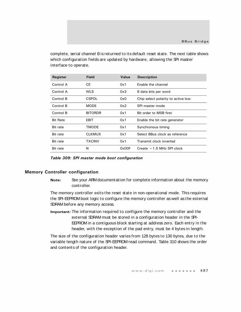
www.d i g i . com 497
BBus B r i d ge
complete, serial channel B is returned to its default reset state. The next table shows which configuration fields are updated by hardware, allowing the SPI master interface to operate.
Memory Controller configuration
Note: See your ARM documentation for complete information about the memory controller.
The memory controller exits the reset state in non-operational mode. This requires the SPI-EEPROM boot logic to configure the memory controller as well as the external SDRAM before any memory access.
Important: The information required to configure the memory controller and the external SDRAM must be stored in a configuration header in the SPI-EEPROM in a contiguous block starting at address zero. Each entry in the header, with the exception of the pad entry, must be 4 bytes in length.
The size of the configuration header varies from 128 bytes to 130 bytes, due to the variable length nature of the SPI-EEPROM read command. Table 310 shows the order and contents of the configuration header.
Register Field Value Description
Control A CE 0x1 Enable the channel
Control A WLS 0x3 8 data bits per word
Control B CSPOL 0x0 Chip select polarity to active low
Control B MODE 0x2 SPI master mode
Control B BITORDR 0x1 Bit order to MSB first
Bit Rate EBIT 0x1 Enable the bit rate generator
Bit rate TMODE 0x1 Synchronous timing
Bit rate CLKMUX 0x1 Select BBus clock as reference
Bit rate TXCINV 0x1 Transmit clock inverted
Bit rate N 0x00F Create ~1.5 MHz SPI clock
Table 309: SPI master mode boot configuration
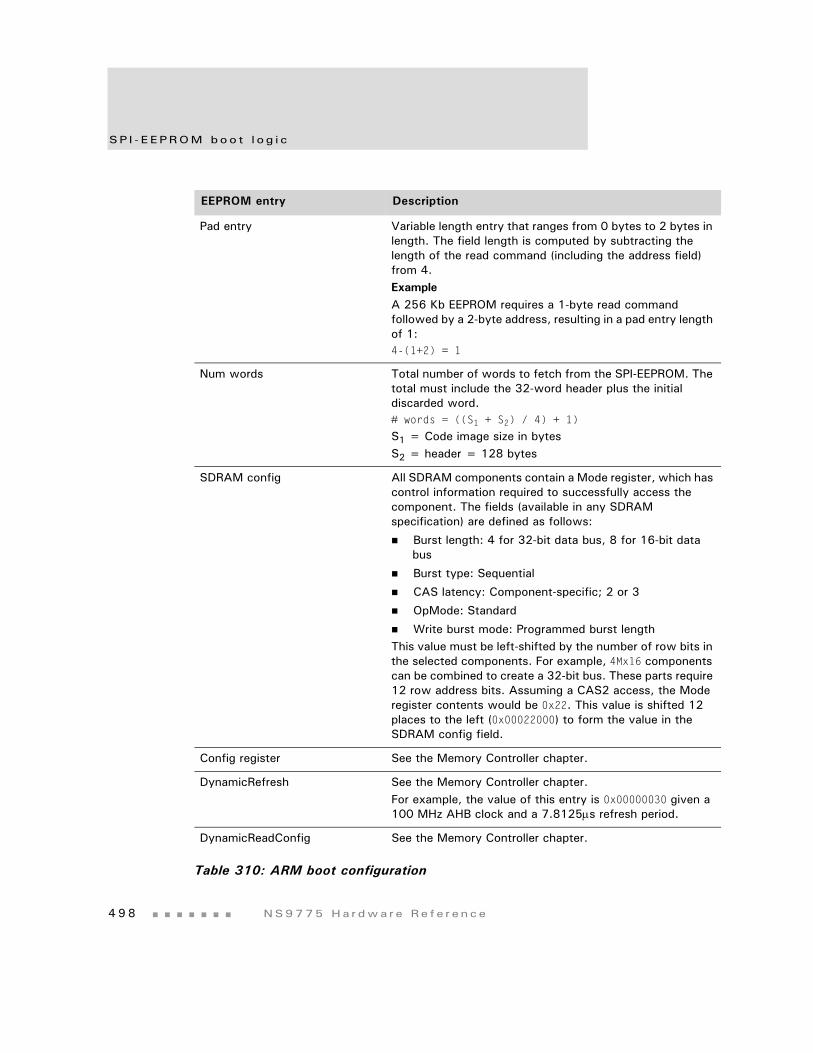
SP I - E EPROM boo t l og i c
4 9 8 NS9775 Ha r dwa r e Re f e r ence
EEPROM entry Description
Pad entry Variable length entry that ranges from 0 bytes to 2 bytes in length. The field length is computed by subtracting the length of the read command (including the address field) from 4. ExampleA 256 Kb EEPROM requires a 1-byte read command followed by a 2-byte address, resulting in a pad entry length of 1:4-(1+2) = 1
Num words Total number of words to fetch from the SPI-EEPROM. The total must include the 32-word header plus the initial discarded word.# words = ((S1 + S2) / 4) + 1)
S1 = Code image size in bytesS2 = header = 128 bytes
SDRAM config All SDRAM components contain a Mode register, which has control information required to successfully access the component. The fields (available in any SDRAM specification) are defined as follows:
Burst length: 4 for 32-bit data bus, 8 for 16-bit data bus
Burst type: Sequential
CAS latency: Component-specific; 2 or 3
OpMode: Standard
Write burst mode: Programmed burst lengthThis value must be left-shifted by the number of row bits in the selected components. For example, 4Mx16 components can be combined to create a 32-bit bus. These parts require 12 row address bits. Assuming a CAS2 access, the Mode register contents would be 0x22. This value is shifted 12 places to the left (0x00022000) to form the value in the SDRAM config field.
Config register See the Memory Controller chapter.
DynamicRefresh See the Memory Controller chapter.For example, the value of this entry is 0x00000030 given a 100 MHz AHB clock and a 7.8125μs refresh period.
DynamicReadConfig See the Memory Controller chapter.
Table 310: ARM boot configuration
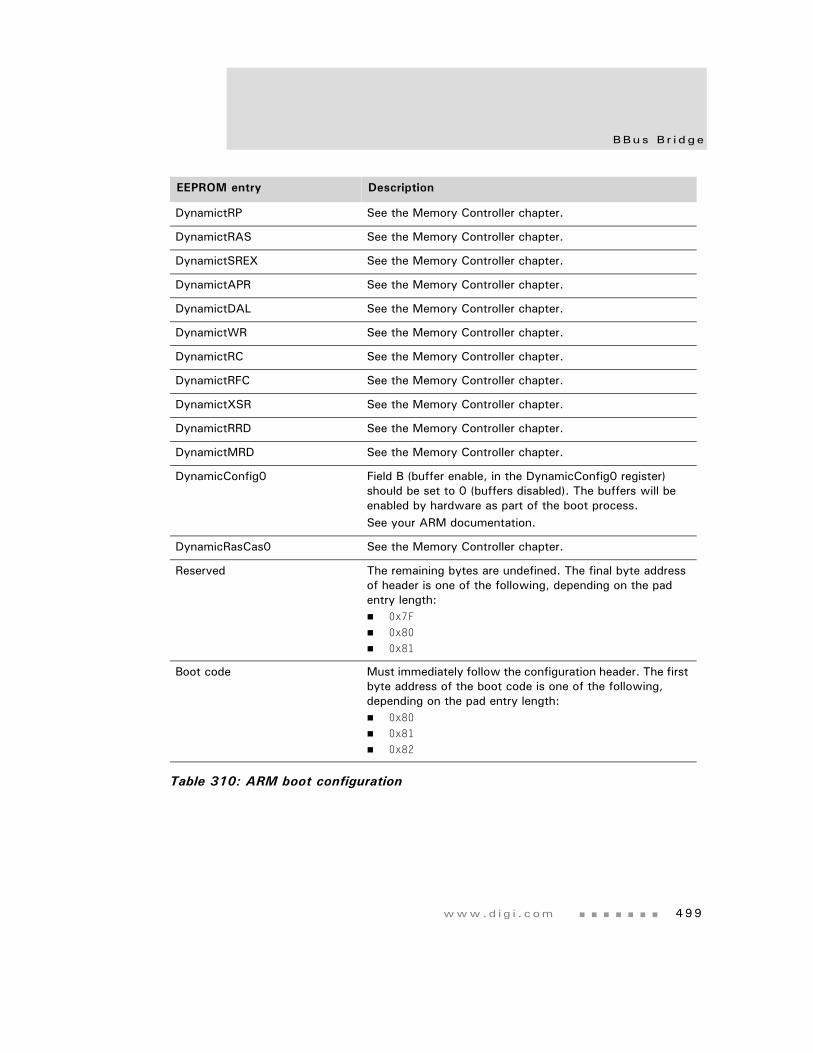
www.d i g i . com 499
BBus B r i d ge
DynamictRP See the Memory Controller chapter.
DynamictRAS See the Memory Controller chapter.
DynamictSREX See the Memory Controller chapter.
DynamictAPR See the Memory Controller chapter.
DynamictDAL See the Memory Controller chapter.
DynamictWR See the Memory Controller chapter.
DynamictRC See the Memory Controller chapter.
DynamictRFC See the Memory Controller chapter.
DynamictXSR See the Memory Controller chapter.
DynamictRRD See the Memory Controller chapter.
DynamictMRD See the Memory Controller chapter.
DynamicConfig0 Field B (buffer enable, in the DynamicConfig0 register) should be set to 0 (buffers disabled). The buffers will be enabled by hardware as part of the boot process. See your ARM documentation.
DynamicRasCas0 See the Memory Controller chapter.
Reserved The remaining bytes are undefined. The final byte address of header is one of the following, depending on the pad entry length: 0x7F
0x80
0x81
Boot code Must immediately follow the configuration header. The first byte address of the boot code is one of the following, depending on the pad entry length: 0x80
0x81
0x82
EEPROM entry Description
Table 310: ARM boot configuration
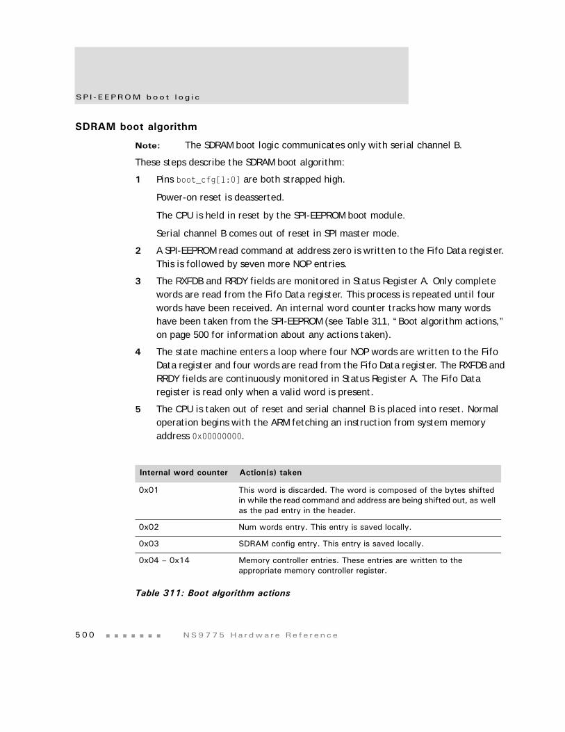
SP I - E EPROM boo t l og i c
5 0 0 NS9775 Ha r dwa r e Re f e r ence
SDRAM boot algorithm
Note: The SDRAM boot logic communicates only with serial channel B.
These steps describe the SDRAM boot algorithm:
1 Pins boot_cfg[1:0] are both strapped high.
Power-on reset is deasserted.
The CPU is held in reset by the SPI-EEPROM boot module.
Serial channel B comes out of reset in SPI master mode.
2 A SPI-EEPROM read command at address zero is written to the Fifo Data register. This is followed by seven more NOP entries.
3 The RXFDB and RRDY fields are monitored in Status Register A. Only complete words are read from the Fifo Data register. This process is repeated until four words have been received. An internal word counter tracks how many words have been taken from the SPI-EEPROM (see Table 311, “Boot algorithm actions,” on page 500 for information about any actions taken).
4 The state machine enters a loop where four NOP words are written to the Fifo Data register and four words are read from the Fifo Data register. The RXFDB and RRDY fields are continuously monitored in Status Register A. The Fifo Data register is read only when a valid word is present.
5 The CPU is taken out of reset and serial channel B is placed into reset. Normal operation begins with the ARM fetching an instruction from system memory address 0x00000000.
Internal word counter Action(s) taken
0x01 This word is discarded. The word is composed of the bytes shifted in while the read command and address are being shifted out, as well as the pad entry in the header.
0x02 Num words entry. This entry is saved locally.
0x03 SDRAM config entry. This entry is saved locally.
0x04 – 0x14 Memory controller entries. These entries are written to the appropriate memory controller register.
Table 311: Boot algorithm actions
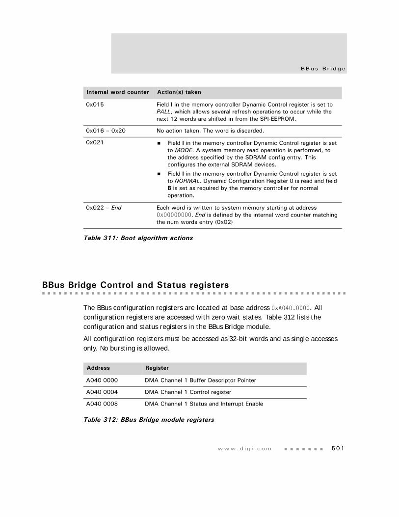
www.d i g i . com 501
BBus B r i d ge
BBus Bridge Control and Status registers
The BBus configuration registers are located at base address 0xA040.0000. All configuration registers are accessed with zero wait states. Table 312 lists the configuration and status registers in the BBus Bridge module.
All configuration registers must be accessed as 32-bit words and as single accesses only. No bursting is allowed.
0x015 Field I in the memory controller Dynamic Control register is set to PALL, which allows several refresh operations to occur while the next 12 words are shifted in from the SPI-EEPROM.
0x016 – 0x20 No action taken. The word is discarded.
0x021 Field I in the memory controller Dynamic Control register is set to MODE. A system memory read operation is performed, to the address specified by the SDRAM config entry. This configures the external SDRAM devices.
Field I in the memory controller Dynamic Control register is set to NORMAL. Dynamic Configuration Register 0 is read and field B is set as required by the memory controller for normal operation.
0x022 – End Each word is written to system memory starting at address 0x00000000. End is defined by the internal word counter matching the num words entry (0x02)
Internal word counter Action(s) taken
Table 311: Boot algorithm actions
Address Register
A040 0000 DMA Channel 1 Buffer Descriptor Pointer
A040 0004 DMA Channel 1 Control register
A040 0008 DMA Channel 1 Status and Interrupt Enable
Table 312: BBus Bridge module registers
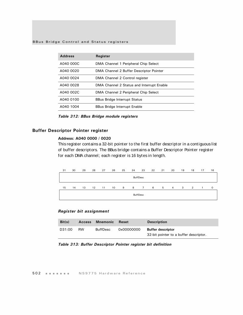
BBus B r i d g e Con t r o l a nd S t a t u s r eg i s t e r s
5 0 2 NS9775 Ha r dwa r e Re f e r ence
Buffer Descriptor Pointer register
Address: A040 0000 / 0020This register contains a 32-bit pointer to the first buffer descriptor in a contiguous list of buffer descriptors. The BBus bridge contains a Buffer Descriptor Pointer register for each DMA channel; each register is 16 bytes in length.
Register bit assignment
A040 000C DMA Channel 1 Peripheral Chip Select
A040 0020 DMA Channel 2 Buffer Descriptor Pointer
A040 0024 DMA Channel 2 Control register
A040 0028 DMA Channel 2 Status and Interrupt Enable
A040 002C DMA Channel 2 Peripheral Chip Select
A040 0100 BBus Bridge Interrupt Status
A040 1004 BBus Bridge Interrupt Enable
Address Register
Table 312: BBus Bridge module registers
Bit(s) Access Mnemonic Reset Description
D31:00 RW BuffDesc 0x00000000 Buffer descriptor32-bit pointer to a buffer descriptor.
Table 313: Buffer Descriptor Pointer register bit definition
13 12 11 10 9 8 7 6 5 4 3 2 1 015 14
31 29 28 27 26 25 24 23 22 21 20 19 18 17 1630
BuffDesc
BuffDesc
www.d i g i . com 503
BBus B r i d ge
DMA Channel 1/2 Control register
Address: A040 0004 / 0024This register contains required DMA transfer control information. The BBus bridge contains a DMA Channel Control register for each channel.
Register bit assignment
Bit(s) Access Mnemonic Reset Description
D31 R/W CE 0 Channel enableEnables and disables DMA operations, as wanted. Write a 1 to this field after a DMA channel has entered the IDLE state for any reason, to initiate additional DMA transfers.
D30 R/W CA 0 Channel abortWhen set, causes the current DMA operation to complete, then closes the buffer.
D29 R/W CG 0 Channel goWhen set, causes the DMA channel to exit the IDLE status and begin a DMA transfer.
Note: The CE field must also be set. This allows software to initiate a memory-to-memory DMA transfer. External peripheral signal REQ is not used during memory-to-memory DMA transfers.
Table 314: DMA Channel 1/2 Control register bit definition
INDEX
13 12 11 10 9 8 7 6 5 4 3 2 1 015 14
Reserved
31 29 28 27 26 25 24 23 22 21 20 19 18 17 1630
CG SB DB SINC_N DINC_NCE CA Not usedSW DW
BBus B r i d g e Con t r o l a nd S t a t u s r eg i s t e r s
5 0 4 NS9775 Ha r dwa r e Re f e r ence
D28:27 R/W SW 0 Source widthDefines the size of the source data bus. Used only for peripheral to memory transfers.00 8 bits01 16 bits10 32 bits11 Undefined
D26:25 R/W DW 0 Destination widthDefines the size of the destination data bus. Used only for memory to peripheral transfers.00 8 bits01 16 bits10 32 bits11 Undefined
D24:23 R/W SB 0 Source burst00 101 2 (Recommended for 8-bit devices)10 4 (Recommended for 16-bit devices)11 8 (Recommended for 32-bit devices)Defines the AHB maximum burst size allowed when reading from the source.
D22:21 R/W DB 0 Destination burst00 101 2 (Recommended for 8-bit devices)10 4 (Recommended for 16-bit devices)11 8 (Recommended for 32-bit devices)Defines the AHB maximum burst size when writing to the destination. This field must be set to the same value as the source burst field.
D20 R/W SINC_N 0 Source address increment0 Increment source address pointer1 Do not increment source address pointerControls whether the source address pointers are incremented after each DMA transfer.
Bit(s) Access Mnemonic Reset Description
Table 314: DMA Channel 1/2 Control register bit definition
www.d i g i . com 505
BBus B r i d ge
D19 R/W DINC_N 0 Destination address increment0 Increment destination address pointer1 Do not increment destination address
pointerControls whether the destination address pointers are incremented after each DMA transfer.
D18:16 R/W POL 0 Always set this field to 0.
D17 R/W MODE 0 Fly-by mode0 Defines a peripheral to memory fly-by
write DMA transfer1 Defines a memory-to-peripheral fly-by read
DMA transferDefines the direction of data movement for fly-by DMA transfers.This field is not used for memory-to-memory DMA transfers initiated by writing the CG field in the DMA Channel 1/2 Control register.
D16 R/W RST 0 ResetForces a reset of the DMA channel. Writing a 1 to this field forces all fields in the DMA Channel 1/2 Control register, except the INDEX field, to the reset state. The INDEX field is written with a value specified on signals ahb_wdat[9:0]. This field always reads back a 0.Writing a 1 to this field while the DMA channel is operational results in unpredictable behavior.
D15:10 N/A Reserved N/A N/A
D09:00 R INDEX 0 Index valueIdentifies the current byte offset pointer relative to the buffer descriptor pointer. This field can be written only when the RST field is being written to a 1.
Bit(s) Access Mnemonic Reset Description
Table 314: DMA Channel 1/2 Control register bit definition
BBus B r i d g e Con t r o l a nd S t a t u s r eg i s t e r s
5 0 6 NS9775 Ha r dwa r e Re f e r ence
DMA Status and Interrupt Enable register
Address: A040 0008 / 0028The DMA Status and Interrupt Enable register contains the DMA transfer status and control information used for generating AHB DMA interrupt signals. The BBus bridge contains a DMA Status and Interrupt Enable register for each DMA channel.
Register bit assignment
Bits Access Mnemonic Reset Description
D31 RW1TC NCIP 0 Normal completion interrupt pendingSet when a buffer descriptor has been closed. A normal DMA completion occurs when the BLEN count expires to 0 and the L bit in the Buffer descriptor is set, or when the peripheral device signals completion.
D30 RW1TC ECIP 0 Error completion interrupt pendingSet when the DMA channel finds either a bad buffer descriptor pointer or a bad data buffer pointer. When ECIP is set, the DMA channel stops until firmware clears the ECIP bit. The DMA channel does not advance to the next buffer descriptor. When firmware clears ECIP, the buffer descriptor is tried again from where it left off. You can use the CA bit in the DMA Channel 1/2 Control register to abort the current buffer descriptor and go to the next buffer descriptor.
Table 315: DMA Status and Interrupt Enable register bit definition
13 12 11 10 9 8 7 6 5 4 3 2 1 015 14
BLEN
31 29 28 27 26 25 24 23 22 21 20 19 18 17 1630
NRIP CAIP PCIP NCIE ECIE NRIE CAIE PCIE WRAP IDONE LAST FULLNCIP ECIP Not used
www.d i g i . com 507
BBus B r i d ge
D29 RW1TC NRIP 0 Buffer not ready interrupt pendingSet when the DMA channel finds a buffer descriptor whose F bit is in the incorrect state. The F bit must be set in order for the fetched buffer descriptor to be considered valid. If the bit is not set, the descriptor is considered invalid and the NRIP bit is set.When NRIP is set, the DMA channel stops until firmware clears the bit. The DMA channel does not advance to the next buffer descriptor.
D28 RW1TC CAIP 0 Channel abort interrupt pendingSet when the DMA channel finds the CA bit set in the DMA Channel 1/2 Control register. When CAIP is set, the DMA channel stops until firmware clears the bit. When CAIP is cleared, the DMA channel automatically advances to the next buffer descriptor. The CA bit must be cleared, through firmware, before CAIP is cleared. Failure to reset the CA bit causes the subsequent buffer descriptor to abort.
D27 RW1TC PCIP 0 Premature complete interrupt pendingSet when a DMA transfer is terminated by assertion of the dma_done signal. NCIP is set when PCIP is set, for backward compatibility.
D26:25 R/W Not used 0 Always set this field to 0.
D24 R/W NCIE 0x0 Enable NCIP interrupt generation
D23 R/W ECIE 0x0 Enable ECIP interrupt generationAlways enable during normal operation.
D22 R/W NRIE 0x0 Enable NRIP interrupt generation
D21 R/W CAIE 0x0 Enable CAIP interrupt generationAlways enable during normal operation.
D20 R/W PCIE 0x0 Enable PCIP interrupt generation
D19 R WRAP 0x0 Debug field, indicating the last descriptor in the buffer descriptor list.
Bits Access Mnemonic Reset Description
Table 315: DMA Status and Interrupt Enable register bit definition
BBus B r i d g e Con t r o l a nd S t a t u s r eg i s t e r s
5 0 8 NS9775 Ha r dwa r e Re f e r ence
DMA Peripheral Chip Select register
Address: A040 000C / 002CThe DMA Peripheral Chip Select register contains the DMA peripheral chip select definition. The BBus bridge contains a DMA Peripheral Chip Select register for each channel.
Register bit assignment
D18 R IDONE 0x0 Debug field, indicating an interrupt on done occurrence.
D17 R LAST 0x0 Debug field, indicating the last buffer descriptor in the current data frame.
D16 R FULL 0x0 Debug field, indicating the status of the F bit from the current DMA buffer descriptor.
D15:00 R BLEN 0x0000 Debug field, indicating the remaining byte transfer count.
Bits Access Mnemonic Reset Description
Table 315: DMA Status and Interrupt Enable register bit definition
Bits Access Mnemonic Reset Description
D31:04 R/W Not used 0 Always set to 0.
D03 R/W POL 0 Chip select polarityDefines the polarity of the memory interface chip select signal (stcsout[n]_n) connected to the external peripheral.0 Defines an active high signal1 Defines an active low signal
Table 316: DMA Peripheral Chip Select register
13 12 11 10 9 8 7 6 5 4 3 2 1 015 14
31 29 28 27 26 25 24 23 22 21 20 19 18 17 1630
Not used
Not used POL Notused SEL
www.d i g i . com 509
BBus B r i d ge
BBus Bridge Interrupt Status register
Address: A040 1000This register contains the interrupt status of the BBus peripherals. All interrupts must be serviced in the originating module.
Register bit assignment
D02 R/W Not used 0 Always set to 0.
D01:00 R/W SEL 0 Chip select selectionDefines which of the four memory interface chip select signals (stcsout[n]_n) is connected to the external peripheral.
Value Chip select0 CS[0]1 CS[1]2 CS[2]3 CS[3]
Note:This field is not used for memory-to-memory transfers.
Bits Access Mnemonic Reset Description
Table 316: DMA Peripheral Chip Select register
Bits Access Mnemonic Reset Description
D31:26 R Not used 00 Always set this field to 0.
D25 R ADMA2 0 AHB DMA channel #2 has asserted its interrupt.
Table 317: BBus Bridge Interrupt Status register
Not used I2C1284 S4TX S4RX S3TX S3RX S2TX S2RX S1TX S1RX USB BBDMA
13 12 11 10 9 8 7 6 5 4 3 2 1 015 14
31 29 28 27 26 25 24 23 22 21 20 19 18 17 1630
ADMA2 ADMA1 Not usedNot used
BBus B r i d g e Con t r o l a nd S t a t u s r eg i s t e r s
5 1 0 NS9775 Ha r dwa r e Re f e r ence
BBus Bridge Interrupt Enable register
Address: A040 1004The BBus Bridge Interrupt Enable register allows you to enable or disable BBus interrupts on an individual basis as well as a global basis. Writing a 1 to a bit enables the interrupt, allowing it to be included in the aggregate signal that is sent to the vector interrupt controller in the System Control module. These fields affect only the generation of the signal sent to the vector interrupt controller (VIC); they do not affect the originating modules.
D24 R ADMA1 0 AHB DMA channel #1 has asserted its interrupt.
D23:13 R Not used 0x000 Always set this field to 0.
D12 R Not used 0 Always write to 0.
D11 R 1284 0 IEEE-1284 module has asserted its interrupt.
D10 R I2C 0 I2C module has asserted its interrupt.
D09 R SDTX 0 SER transmit module D has asserted its interrupt.
D08 R SDRX 0 SER receive module D has asserted its interrupt.
D07 R SCTX 0 SER transmit module C has asserted its interrupt.
D06 R SCRX 0 SER receive module C has asserted its interrupt.
D05 R SATX 0 SER transmit module A has asserted its interrupt.
D04 R SARX 0 SER receive module A has asserted its interrupt.
D03 R SBTX 0 SER transmit module B has asserted its interrupt.
D02 R SBRX 0 SER receive module B has asserted its interrupt.
D01 R USB 0 USB module has asserted its interrupt.
D00 R BBDMA 0 BBus DMA module has asserted its interrupt.
Bits Access Mnemonic Reset Description
Table 317: BBus Bridge Interrupt Status register
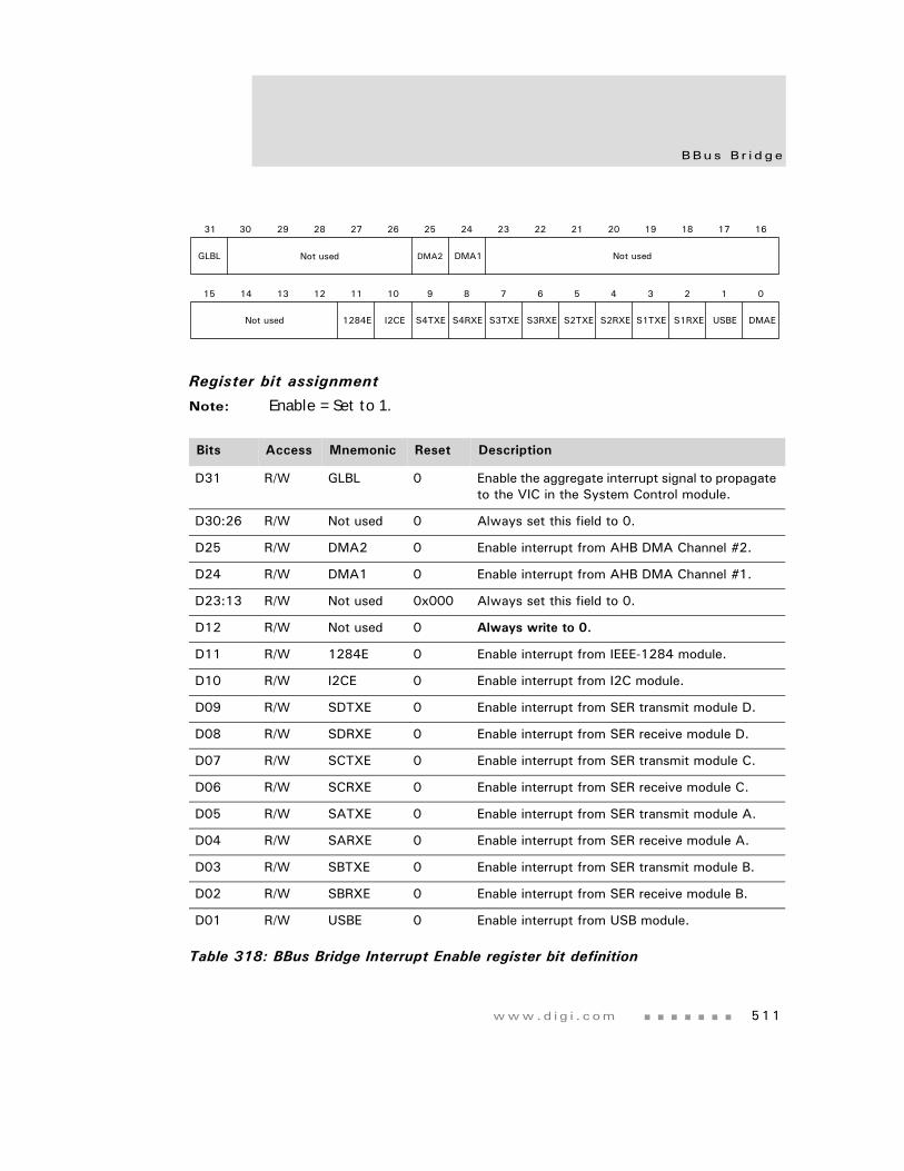
www.d i g i . com 511
BBus B r i d ge
Register bit assignment
Note: Enable = Set to 1.
Bits Access Mnemonic Reset Description
D31 R/W GLBL 0 Enable the aggregate interrupt signal to propagate to the VIC in the System Control module.
D30:26 R/W Not used 0 Always set this field to 0.
D25 R/W DMA2 0 Enable interrupt from AHB DMA Channel #2.
D24 R/W DMA1 0 Enable interrupt from AHB DMA Channel #1.
D23:13 R/W Not used 0x000 Always set this field to 0.
D12 R/W Not used 0 Always write to 0.
D11 R/W 1284E 0 Enable interrupt from IEEE-1284 module.
D10 R/W I2CE 0 Enable interrupt from I2C module.
D09 R/W SDTXE 0 Enable interrupt from SER transmit module D.
D08 R/W SDRXE 0 Enable interrupt from SER receive module D.
D07 R/W SCTXE 0 Enable interrupt from SER transmit module C.
D06 R/W SCRXE 0 Enable interrupt from SER receive module C.
D05 R/W SATXE 0 Enable interrupt from SER transmit module A.
D04 R/W SARXE 0 Enable interrupt from SER receive module A.
D03 R/W SBTXE 0 Enable interrupt from SER transmit module B.
D02 R/W SBRXE 0 Enable interrupt from SER receive module B.
D01 R/W USBE 0 Enable interrupt from USB module.
Table 318: BBus Bridge Interrupt Enable register bit definition
Not used I2CE1284E S4TXE S4RXE S3TXE S3RXE S2TXE S2RXE S1TXE S1RXE USBE DMAE
13 12 11 10 9 8 7 6 5 4 3 2 1 015 14
31 29 28 27 26 25 24 23 22 21 20 19 18 17 1630
DMA2 DMA1 Not usedNot usedGLBL
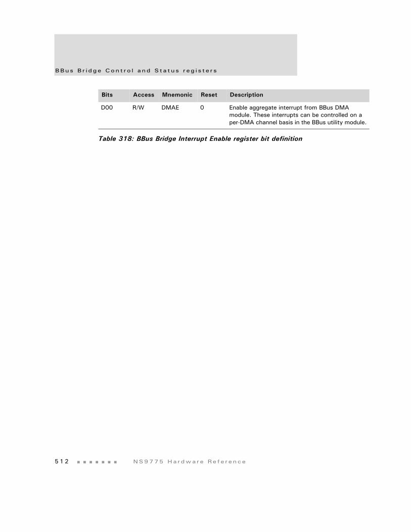
BBus B r i d g e Con t r o l a nd S t a t u s r eg i s t e r s
5 1 2 NS9775 Ha r dwa r e Re f e r ence
D00 R/W DMAE 0 Enable aggregate interrupt from BBus DMA module. These interrupts can be controlled on a per-DMA channel basis in the BBus utility module.
Bits Access Mnemonic Reset Description
Table 318: BBus Bridge Interrupt Enable register bit definition
513
C H A P T E R 9
The NS9775 ASIC BBus subsystem contains two DMA controllers, each with 16 channels.
Note: These DMA controllers are different than the AHB DMA controllers discussed in the BBus Bridge chapter.
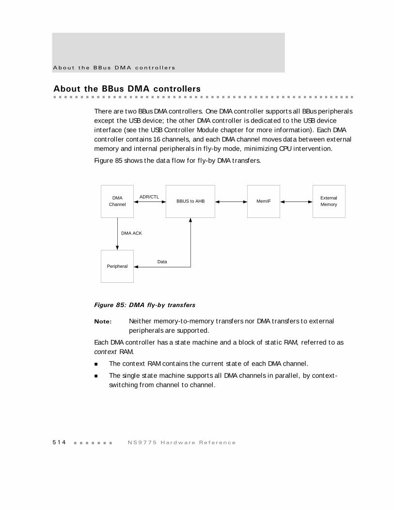
Abou t t h e BBus DMA con t r o l l e r s
5 1 4 NS9775 Ha r dwa r e Re f e r ence
About the BBus DMA controllers
There are two BBus DMA controllers. One DMA controller supports all BBus peripherals except the USB device; the other DMA controller is dedicated to the USB device interface (see the USB Controller Module chapter for more information). Each DMA controller contains 16 channels, and each DMA channel moves data between external memory and internal peripherals in fly-by mode, minimizing CPU intervention.
Figure 85 shows the data flow for fly-by DMA transfers.
Figure 85: DMA fly-by transfers
Note: Neither memory-to-memory transfers nor DMA transfers to external peripherals are supported.
Each DMA controller has a state machine and a block of static RAM, referred to as context RAM.
The context RAM contains the current state of each DMA channel.
The single state machine supports all DMA channels in parallel, by context-switching from channel to channel.
ExternalMemory
DMAChannel
PeripheralData
DMA ACK
BBUS to AHB MemIFADR/CTL
www.d i g i . com 515
BBus DMA Con t r o l l e r
Figure 86 shows the BBus DMA controller block.
Figure 86: DMA controller block
Each DMA controller arbiter determines in which channel the state machine currently is operating.
DMA context memory
Each DMA controller maintains state for all 16 channels using an on-chip SRAM known as the context memory. One 128x32 single port SRAM macrocell comprises this memory. Table 319 defines the entries that describe the state of each DMA channel.
BBUS Interface
BBUS
ChannelTransferAttributes
DMAChannelArbiter
DMAControl
State Machine DMAContext
RAM128x32
DMA bu f f e r d e s c r i p t o r
5 1 6 NS9775 Ha r dwa r e Re f e r ence
DMA buffer descriptor
All DMA channels operate using a buffer descriptor. Each DMA channel remains idle until enabled through the DMA Channel Control register. When a DMA channel is activated, it reads the DMA buffer descriptor pointed to by the Buffer Descriptor Pointer register. When the current descriptor is retired, the next descriptor is accessed from a circular buffer.
Each DMA buffer descriptor is four 32-bit words in length. Multiple buffer descriptors are located in circular buffers of 1024 bytes, with a maximum of 64 buffer descriptors. The DMA channel’s buffer descriptor pointer provides the first buffer descriptor address. Subsequent buffer descriptors are found adjacent to the first descriptor. The final buffer descriptor is defined with its W bit set. When the DMA channel encounters the W bit, the channel wraps around to the first descriptor.
Note: Configuring a DMA channel for more than the maximum number of buffer descriptors results in unpredictable behavior.
Figure 87 shows the DMA buffer descriptor. Table 320 explains each buffer descriptor component.
Offset Description
0x00 Buffer descriptor pointer
0x01 Control register
0x02 Status register
0x03 Unused
0x04 Source Address register
0x05 Buffer Length register
0x06 Destination Address register
0x07 Control flags and transfer status
Table 319: DMA context memory entry
www.d i g i . com 517
BBus DMA Con t r o l l e r
Figure 87: DMA buffer descriptor
Field Description
Source address Identifies the starting location of the source data buffer.
For transmit buffers. The source address can start on any byte boundary.
For receive buffers. The source address must be word-aligned.Be sure the source address field points to an existing memory location.
Buffer length Indicates, in fly-by peripheral-to-memory operations, the maximum number of bytes available in the receive buffer pointed to by the source buffer pointer. After filling a receive buffer with peripheral data, the DMA controller updates this field with the initial buffer length less the actual receive data byte count.
Note: The buffer length must be a multiple of four bytes.
Indicates, in fly-by memory-to-peripheral operations, the number of bytes to move from the source address pointer to the peripheral device. After completing a transmit buffer descriptor, the DMA controller updates this field with the initial buffer length less the actual transmit data byte count (useful for error conditions).
In either mode, this field is limited to 16 bits, which supports a maximum transfer size of 65535 bytes.
Destination address This field is not used in BBus DMA transfers. The field is updated with all zeroes when the descriptor is retired.
Table 320: DMA buffer descriptor definition
Destination Address
Buffer Length
Status
Source Address
0
OFFSET + 0
OFFSET + 4
OFFSET + 8
OFFSET + C FI LW Reserved
31 30 29 28 16 15
Reserved
DMA bu f f e r d e s c r i p t o r
5 1 8 NS9775 Ha r dwa r e Re f e r ence
W The wrap bit. When set, this bit informs the DMA controller that this is the last buffer descriptor within the continuous list of descriptors for the channel. The next buffer descriptor is found using the initial DMA channel buffer descriptor pointer. When the WRAP bit is not set, the next buffer descriptor is found using a 16 byte offset from the current buffer descriptor.
I The interrupt bit. When set, this bit tells the DMA controller to issue an interrupt to the CPU when the buffer is closed due to a normal channel completion. The interrupt occurs no matter what the normal completion interrupt enable configuration is for the DMA channel.
L The last bit. This bit indicates end-of-packet status.
In fly-by peripheral-to-memory operations, this bit indicates that the buffer was closed due to an end-of-packet status signal from the peripheral to the DMA controller.
In fly-by memory-to-peripheral operations, this bit indicates to the DMA controller that this buffer descriptor marks the end of the packet.
Note: For USB-IN transactions (DMA read), this bit must always be set to 1.
F The full bit. When set, this bit indicates that the buffer is full. A DMA channel sets this bit after filling a buffer. A DMA channel clears this bit after emptying a buffer.A DMA channel does not try to empty a buffer with the F bit clear. Similarly, a DMA channel does not try to fill a buffer with the F bit set.When firmware modifies the F bit, the firmware also must write a 1 to the CE bit in the DMA Channel Control register to activate the idle channel.
Reserved You must write a 0 to this field.
Status 16-bit status field. The USB and serial controllers use this field to store transmit and receive status words that result from a completed transmit or receive data frame.
Be advised: The BBus DMA buffer descriptor status field may not reflect the occurrence of a receive overrun in the serial module.
Field Description
Table 320: DMA buffer descriptor definition
www.d i g i . com 519
BBus DMA Con t r o l l e r
DMA transfer status
The DMA buffer descriptor status field is updated when the buffer descriptor is retired. Tables 321 through 326 provide a brief description of the 16-bit status fields for each peripheral. See the appropriate chapters in this manual for more information about each bit.
Bits Mnemonic Description
15 MATCH1 Receive character match #1
14 MATCH2 Receive character match #2
13 MATCH3 Receive character match #3
12 MATCH4 Receive character match #4
11 BGAP Buffer gap timeout
10 CGAP Character gap timeout
09:04 UNUSED Not used — read back 0
03 RBRK Receive line break
02 RFE Receive frame error
01 RPE Receive parity error
00 ROVER Receive overrun error
Table 321: Peripheral bit fields: Serial controller — UART RX mode
Bits Mnemonic Description
15 MATCH1 Receive character match #1
14 MATCH2 Receive character match #2
13 MATCH3 Receive character match #3
12 MATCH4 Receive character match #4
11:00 UNUSED Not used — read back 0
Table 322: Peripheral bit fields: Serial controller — SPI RX mode
DMA bu f f e r d e s c r i p t o r
5 2 0 NS9775 Ha r dwa r e Re f e r ence
Bits Mnemonic Description
15:00 UNUSED Not used — read back 0
Table 323: Peripheral bit fields: Serial controller — UART TX mode
Bits Mnemonic Description
15:00 UNUSED Not used — read back 0
Table 324: Peripheral bit fields: Serial controller — SPI TX mode
Bits Mnemonic Description
15:14 STATE 00 Undefined01 Data phase transaction10 Status phase transaction11 No-data status phase transactionDefines the state of the endpoint after the most recent communication with the USB device module. This field is used primarily for debugging.
13 M31 See the USB Controller module chapter.
12 M30 See the USB Controller module chapter.
11:00 CIA If field M30 equals 1, this field contains the least significant 12 bits of the Setup command address. Because all Setup command addresses are required to be in the format ???, where ??? is not equal to 000, the most significant nibble is zero.If the M30 field equals 0, this field contains the configuration, interface, and alternate information for the specified endpoint.
Table 325: Peripheral bit fields: USB device controller
www.d i g i . com 521
BBus DMA Con t r o l l e r
DMA channel assignments
Each BBus DMA controller contains 16 DMA channels. Controller DMA1 is dedicated to the BBus peripherals. Controller DMA2 is dedicated to the USB device endpoints. Any given DMA channel is hard-wired to a peripheral.
Table 327 indicates which peripherals are hard-wired to which DMA channels, and the DMA mode (direction) required for each. These are the DMA modes:
FBR — Fly-by memory-to-peripheral
FBW — Fly-by peripheral-to-memory
FBRW — Fly-by programmable for either direction
Bits Mnemonic Description
15:00 UNUSED Not used — read back 0
Table 326: Peripheral bit fields: IEEE 1284 controller
DMA Channel DMA channel peripheral Fly-by direction
DMA1 1 SER channel B receiver FBW
DMA1 2 SER channel B transmitter FBR
DMA1 3 SER channel A receiver FBW
DMA1 4 SER channel A transmitter FBR
DMA1 5 SER channel C receiver FBW
DMA1 6 SER channel C transmitter FBR
DMA1 7 SER channel D receiver FBW
DMA1 8 SER channel D transmitter FBR
DMA1 9 1284 command receiver FBW
DMA1 10 Unused N/A
Table 327: DMA channel assignments
DMA channe l a s s i g nmen t s
5 2 2 NS9775 Ha r dwa r e Re f e r ence
DMA1 11 1284 data receiver FBW
DMA1 12 1284 data transmitter FBR
DMA1 13 Unused N/A
DMA1 14 Unused N/A
DMA1 15 Unused N/A
DMA1 16 Unused N/A
DMA2 1 USB device control-OUT endpoint #0 FBW
DMA2 2 USB device control-IN endpoint #0 FBR
DMA2 3 USB device endpoint#1 FBRW
DMA2 4 USB device endpoint#2 FBRW
DMA2 5 USB device endpoint#3 FBRW
DMA2 6 USB device endpoint#4 FBRW
DMA2 7 USB device endpoint#5 FBRW
DMA2 8 USB device endpoint#6 FBRW
DMA2 9 USB device endpoint#7 FBRW
DMA2 10 USB device endpoint#8 FBRW
DMA2 11 USB device endpoint#9 FBRW
DMA2 12 USB device endpoint#10 FBRW
DMA2 13 USB device endpoint#11 FBRW
DMA2 14 Unused N/A
DMA2 15 Unused N/A
DMA2 16 Unused N/A
DMA Channel DMA channel peripheral Fly-by direction
Table 327: DMA channel assignments
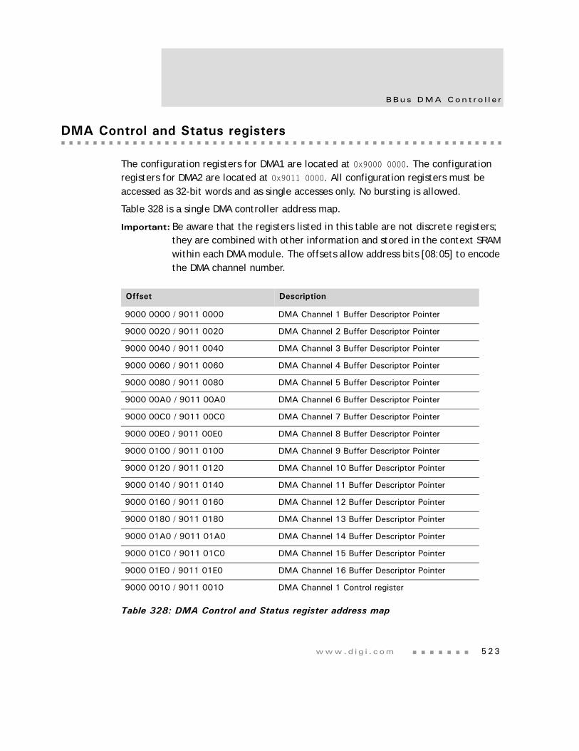
www.d i g i . com 523
BBus DMA Con t r o l l e r
DMA Control and Status registers
The configuration registers for DMA1 are located at 0x9000 0000. The configuration registers for DMA2 are located at 0x9011 0000. All configuration registers must be accessed as 32-bit words and as single accesses only. No bursting is allowed.
Table 328 is a single DMA controller address map.
Important: Be aware that the registers listed in this table are not discrete registers; they are combined with other information and stored in the context SRAM within each DMA module. The offsets allow address bits [08:05] to encode the DMA channel number.
Offset Description
9000 0000 / 9011 0000 DMA Channel 1 Buffer Descriptor Pointer
9000 0020 / 9011 0020 DMA Channel 2 Buffer Descriptor Pointer
9000 0040 / 9011 0040 DMA Channel 3 Buffer Descriptor Pointer
9000 0060 / 9011 0060 DMA Channel 4 Buffer Descriptor Pointer
9000 0080 / 9011 0080 DMA Channel 5 Buffer Descriptor Pointer
9000 00A0 / 9011 00A0 DMA Channel 6 Buffer Descriptor Pointer
9000 00C0 / 9011 00C0 DMA Channel 7 Buffer Descriptor Pointer
9000 00E0 / 9011 00E0 DMA Channel 8 Buffer Descriptor Pointer
9000 0100 / 9011 0100 DMA Channel 9 Buffer Descriptor Pointer
9000 0120 / 9011 0120 DMA Channel 10 Buffer Descriptor Pointer
9000 0140 / 9011 0140 DMA Channel 11 Buffer Descriptor Pointer
9000 0160 / 9011 0160 DMA Channel 12 Buffer Descriptor Pointer
9000 0180 / 9011 0180 DMA Channel 13 Buffer Descriptor Pointer
9000 01A0 / 9011 01A0 DMA Channel 14 Buffer Descriptor Pointer
9000 01C0 / 9011 01C0 DMA Channel 15 Buffer Descriptor Pointer
9000 01E0 / 9011 01E0 DMA Channel 16 Buffer Descriptor Pointer
9000 0010 / 9011 0010 DMA Channel 1 Control register
Table 328: DMA Control and Status register address map
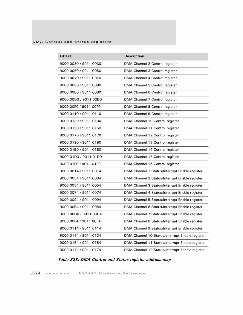
DMA Con t r o l a nd S t a t u s r e g i s t e r s
5 2 4 NS9775 Ha r dwa r e Re f e r ence
9000 0030 / 9011 0030 DMA Channel 2 Control register
9000 0050 / 9011 0050 DMA Channel 3 Control register
9000 0070 / 9011 0070 DMA Channel 4 Control register
9000 0090 / 9011 0090 DMA Channel 5 Control register
9000 00B0 / 9011 00B0 DMA Channel 6 Control register
9000 00D0 / 9011 00D0 DMA Channel 7 Control register
9000 00F0 / 9011 00F0 DMA Channel 8 Control register
9000 0110 / 9011 0110 DMA Channel 9 Control register
9000 0130 / 9011 0130 DMA Channel 10 Control register
9000 0150 / 9011 0150 DMA Channel 11 Control register
9000 0170 / 9011 0170 DMA Channel 12 Control register
9000 0190 / 9011 0190 DMA Channel 13 Control register
9000 01B0 / 9011 01B0 DMA Channel 14 Control register
9000 01D0 / 9011 01D0 DMA Channel 15 Control register
9000 01F0 / 9011 01F0 DMA Channel 16 Control register
9000 0014 / 9011 0014 DMA Channel 1 Status/Interrupt Enable register
9000 0034 / 9011 0034 DMA Channel 2 Status/Interrupt Enable register
9000 0054 / 9011 0054 DMA Channel 3 Status/Interrupt Enable register
9000 0074 / 9011 0074 DMA Channel 4 Status/Interrupt Enable register
9000 0094 / 9011 0094 DMA Channel 5 Status/Interrupt Enable register
9000 00B4 / 9011 00B4 DMA Channel 6 Status/Interrupt Enable register
9000 00D4 / 9011 00D4 DMA Channel 7 Status/Interrupt Enable register
9000 00F4 / 9011 00F4 DMA Channel 8 Status/Interrupt Enable register
9000 0114 / 9011 0114 DMA Channel 9 Status/Interrupt Enable register
9000 0134 / 9011 0134 DMA Channel 10 Status/Interrupt Enable register
9000 0154 / 9011 0154 DMA Channel 11 Status/Interrupt Enable register
9000 0174 / 9011 0174 DMA Channel 12 Status/Interrupt Enable register
Offset Description
Table 328: DMA Control and Status register address map
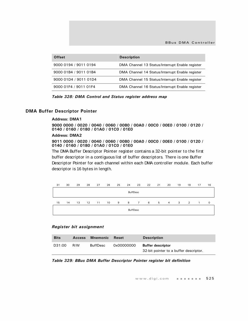
www.d i g i . com 525
BBus DMA Con t r o l l e r
DMA Buffer Descriptor Pointer
Address: DMA1
9000 0000 / 0020 / 0040 / 0060 / 0080 / 00A0 / 00C0 / 00E0 / 0100 / 0120 / 0140 / 0160 / 0180 / 01A0 / 01C0 / 01E0
Address: DMA2
9011 0000 / 0020 / 0040 / 0060 / 0080 / 00A0 / 00C0 / 00E0 / 0100 / 0120 / 0140 / 0160 / 0180 / 01A0 / 01C0 / 01E0The DMA Buffer Descriptor Pointer register contains a 32-bit pointer to the first buffer descriptor in a contiguous list of buffer descriptors. There is one Buffer Descriptor Pointer for each channel within each DMA controller module. Each buffer descriptor is 16 bytes in length.
Register bit assignment
9000 0194 / 9011 0194 DMA Channel 13 Status/Interrupt Enable register
9000 01B4 / 9011 01B4 DMA Channel 14 Status/Interrupt Enable register
9000 01D4 / 9011 01D4 DMA Channel 15 Status/Interrupt Enable register
9000 01F4 / 9011 01F4 DMA Channel 16 Status/Interrupt Enable register
Offset Description
Table 328: DMA Control and Status register address map
Bits Access Mnemonic Reset Description
D31:00 R/W BuffDesc 0x00000000 Buffer descriptor32-bit pointer to a buffer descriptor.
Table 329: BBus DMA Buffer Descriptor Pointer register bit definition
13 12 11 10 9 8 7 6 5 4 3 2 1 015 14
31 29 28 27 26 25 24 23 22 21 20 19 18 17 1630
BuffDesc
BuffDesc
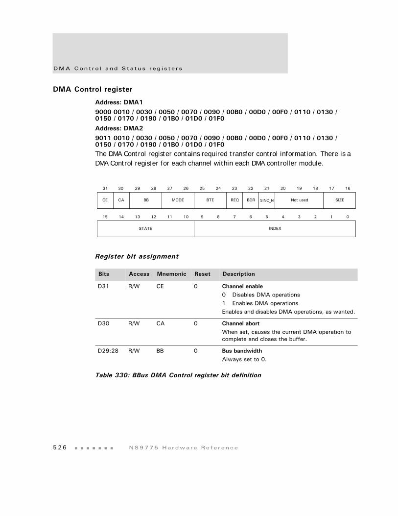
DMA Con t r o l a nd S t a t u s r e g i s t e r s
5 2 6 NS9775 Ha r dwa r e Re f e r ence
DMA Control register
Address: DMA1
9000 0010 / 0030 / 0050 / 0070 / 0090 / 00B0 / 00D0 / 00F0 / 0110 / 0130 / 0150 / 0170 / 0190 / 01B0 / 01D0 / 01F0
Address: DMA2
9011 0010 / 0030 / 0050 / 0070 / 0090 / 00B0 / 00D0 / 00F0 / 0110 / 0130 / 0150 / 0170 / 0190 / 01B0 / 01D0 / 01F0The DMA Control register contains required transfer control information. There is a DMA Control register for each channel within each DMA controller module.
Register bit assignment
Bits Access Mnemonic Reset Description
D31 R/W CE 0 Channel enable0 Disables DMA operations1 Enables DMA operationsEnables and disables DMA operations, as wanted.
D30 R/W CA 0 Channel abortWhen set, causes the current DMA operation to complete and closes the buffer.
D29:28 R/W BB 0 Bus bandwidthAlways set to 0.
Table 330: BBus DMA Control register bit definition
13 12 11 10 9 8 7 6 5 4 3 2 1 015 14
STATE
31 29 28 27 26 25 24 23 22 21 20 19 18 17 1630
BB Not usedREQ BDRCE CA SIZE
INDEX
MODE BTE SINC_N
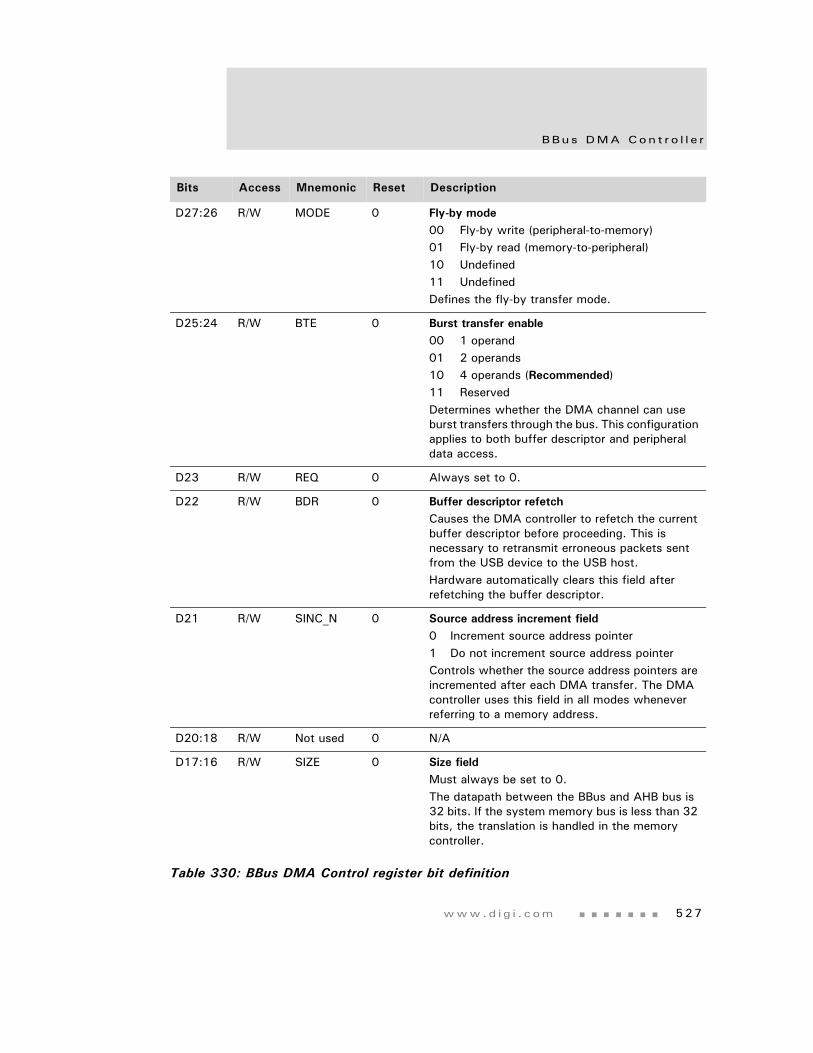
www.d i g i . com 527
BBus DMA Con t r o l l e r
D27:26 R/W MODE 0 Fly-by mode00 Fly-by write (peripheral-to-memory)01 Fly-by read (memory-to-peripheral)10 Undefined11 UndefinedDefines the fly-by transfer mode.
D25:24 R/W BTE 0 Burst transfer enable00 1 operand01 2 operands10 4 operands (Recommended)11 ReservedDetermines whether the DMA channel can use burst transfers through the bus. This configuration applies to both buffer descriptor and peripheral data access.
D23 R/W REQ 0 Always set to 0.
D22 R/W BDR 0 Buffer descriptor refetchCauses the DMA controller to refetch the current buffer descriptor before proceeding. This is necessary to retransmit erroneous packets sent from the USB device to the USB host. Hardware automatically clears this field after refetching the buffer descriptor.
D21 R/W SINC_N 0 Source address increment field0 Increment source address pointer1 Do not increment source address pointerControls whether the source address pointers are incremented after each DMA transfer. The DMA controller uses this field in all modes whenever referring to a memory address.
D20:18 R/W Not used 0 N/A
D17:16 R/W SIZE 0 Size fieldMust always be set to 0. The datapath between the BBus and AHB bus is 32 bits. If the system memory bus is less than 32 bits, the translation is handled in the memory controller.
Bits Access Mnemonic Reset Description
Table 330: BBus DMA Control register bit definition
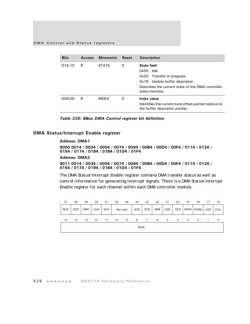
DMA Con t r o l a nd S t a t u s r e g i s t e r s
5 2 8 NS9775 Ha r dwa r e Re f e r ence
DMA Status/Interrupt Enable register
Address: DMA1
9000 0014 / 0034 / 0054 / 0074 / 0094 / 00B4 / 00D4 / 00F4 / 0114 / 0134 / 0154 / 0174 / 0194 / 01B4 / 01D4 / 01F4
Address: DMA2
9011 0014 / 0034 / 0054 / 0074 / 0094 / 00B4 / 00D4 / 00F4 / 0114 / 0134 / 0154 / 0174 / 0194 / 01B4 / 01D4 / 01F4
The DMA Status/Interrupt Enable register contains DMA transfer status as well as control information for generating interrupt signals. There is a DMA Status/Interrupt Enable register for each channel within each DMA controller module.
D15:10 R STATE 0 State field0x00 Idle0x20 Transfer in progress0x18 Update buffer descriptorDescribes the current state of the DMA controller state machine.
D09:00 R INDEX 0 Index valueIdentifies the current byte offset pointer relative to the buffer descriptor pointer.
Bits Access Mnemonic Reset Description
Table 330: BBus DMA Control register bit definition
13 12 11 10 9 8 7 6 5 4 3 2 1 015 14
31 29 28 27 26 25 24 23 22 21 20 19 18 17 1630
ECIE NRIENCIP ECIP
BLEN
PCIECAIENRIP CAIP PCIP Not used NCIE WRAP IDONE LAST FULL
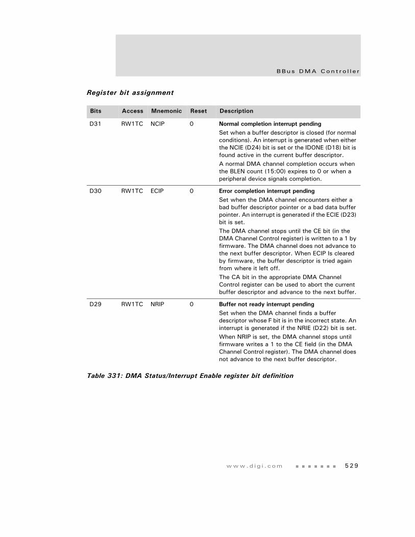
www.d i g i . com 529
BBus DMA Con t r o l l e r
Register bit assignment
Bits Access Mnemonic Reset Description
D31 RW1TC NCIP 0 Normal completion interrupt pendingSet when a buffer descriptor is closed (for normal conditions). An interrupt is generated when either the NCIE (D24) bit is set or the IDONE (D18) bit is found active in the current buffer descriptor.A normal DMA channel completion occurs when the BLEN count (15:00) expires to 0 or when a peripheral device signals completion.
D30 RW1TC ECIP 0 Error completion interrupt pendingSet when the DMA channel encounters either a bad buffer descriptor pointer or a bad data buffer pointer. An interrupt is generated if the ECIE (D23) bit is set. The DMA channel stops until the CE bit (in the DMA Channel Control register) is written to a 1 by firmware. The DMA channel does not advance to the next buffer descriptor. When ECIP Is cleared by firmware, the buffer descriptor is tried again from where it left off. The CA bit in the appropriate DMA Channel Control register can be used to abort the current buffer descriptor and advance to the next buffer.
D29 RW1TC NRIP 0 Buffer not ready interrupt pendingSet when the DMA channel finds a buffer descriptor whose F bit is in the incorrect state. An interrupt is generated if the NRIE (D22) bit is set.When NRIP is set, the DMA channel stops until firmware writes a 1 to the CE field (in the DMA Channel Control register). The DMA channel does not advance to the next buffer descriptor.
Table 331: DMA Status/Interrupt Enable register bit definition
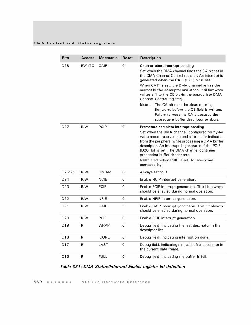
DMA Con t r o l a nd S t a t u s r e g i s t e r s
5 3 0 NS9775 Ha r dwa r e Re f e r ence
D28 RW1TC CAIP 0 Channel abort interrupt pendingSet when the DMA channel finds the CA bit set in the DMA Channel Control register. An interrupt is generated when the CAIE (D21) bit is set.When CAIP Is set, the DMA channel retires the current buffer descriptor and stops until firmware writes a 1 to the CE bit (in the appropriate DMA Channel Control register).
Note: The CA bit must be cleared, using firmware, before the CE field is written. Failure to reset the CA bit causes the subsequent buffer descriptor to abort.
D27 R/W PCIP 0 Premature complete interrupt pendingSet when the DMA channel, configured for fly-by write mode, receives an end-of-transfer indicator from the peripheral while processing a DMA buffer descriptor. An interrupt is generated if the PCIE (D20) bit is set. The DMA channel continues processing buffer descriptors.NCIP is set when PCIP is set, for backward compatibility.
D26:25 R/W Unused 0 Always set to 0.
D24 R/W NCIE 0 Enable NCIP interrupt generation.
D23 R/W ECIE 0 Enable ECIP interrupt generation. This bit always should be enabled during normal operation.
D22 R/W NRIE 0 Enable NRIP interrupt generation.
D21 R/W CAIE 0 Enable CAIP interrupt generation. This bit always should be enabled during normal operation.
D20 R/W PCIE 0 Enable PCIP interrupt generation.
D19 R WRAP 0 Debug field, indicating the last descriptor in the descriptor list.
D18 R IDONE 0 Debug field, indicating interrupt on done.
D17 R LAST 0 Debug field, indicating the last buffer descriptor in the current data frame.
D16 R FULL 0 Debug field, indicating the buffer is full.
Bits Access Mnemonic Reset Description
Table 331: DMA Status/Interrupt Enable register bit definition
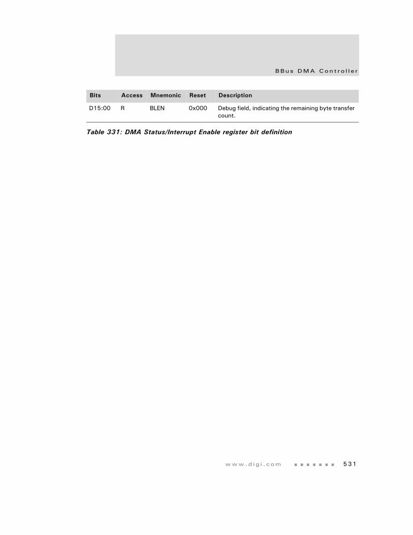
www.d i g i . com 531
BBus DMA Con t r o l l e r
D15:00 R BLEN 0x000 Debug field, indicating the remaining byte transfer count.
Bits Access Mnemonic Reset Description
Table 331: DMA Status/Interrupt Enable register bit definition

533
BBus UtilityC H A P T E R 1 0
The BBus utility provides chip-level support for the low speed peripherals in the NS9775 ASIC that reside on the Digi proprietary BBus. The BBus utility handles functions such as bus monitors, GPIO control, and peripheral reset.
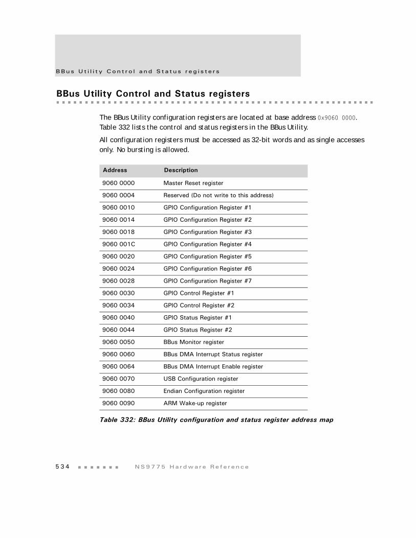
BBus U t i l i t y Con t r o l a nd S t a t u s r e g i s t e r s
5 3 4 NS9775 Ha r dwa r e Re f e r ence
BBus Utility Control and Status registers
The BBus Utility configuration registers are located at base address 0x9060 0000. Table 332 lists the control and status registers in the BBus Utility.
All configuration registers must be accessed as 32-bit words and as single accesses only. No bursting is allowed.
Address Description
9060 0000 Master Reset register
9060 0004 Reserved (Do not write to this address)
9060 0010 GPIO Configuration Register #1
9060 0014 GPIO Configuration Register #2
9060 0018 GPIO Configuration Register #3
9060 001C GPIO Configuration Register #4
9060 0020 GPIO Configuration Register #5
9060 0024 GPIO Configuration Register #6
9060 0028 GPIO Configuration Register #7
9060 0030 GPIO Control Register #1
9060 0034 GPIO Control Register #2
9060 0040 GPIO Status Register #1
9060 0044 GPIO Status Register #2
9060 0050 BBus Monitor register
9060 0060 BBus DMA Interrupt Status register
9060 0064 BBus DMA Interrupt Enable register
9060 0070 USB Configuration register
9060 0080 Endian Configuration register
9060 0090 ARM Wake-up register
Table 332: BBus Utility configuration and status register address map
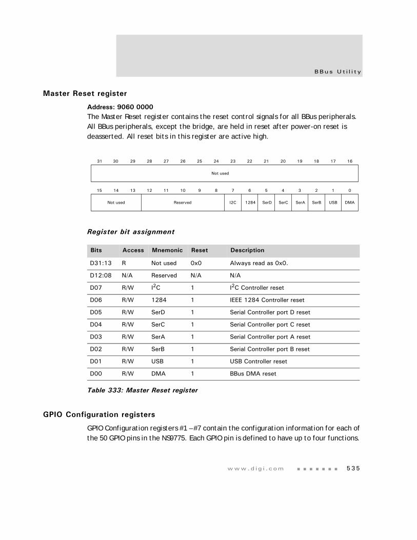
www.d i g i . com 535
BBus U t i l i t y
Master Reset register
Address: 9060 0000The Master Reset register contains the reset control signals for all BBus peripherals. All BBus peripherals, except the bridge, are held in reset after power-on reset is deasserted. All reset bits in this register are active high.
Register bit assignment
GPIO Configuration registers
GPIO Configuration registers #1 – #7 contain the configuration information for each of the 50 GPIO pins in the NS9775. Each GPIO pin is defined to have up to four functions.
Bits Access Mnemonic Reset Description
D31:13 R Not used 0x0 Always read as 0x0.
D12:08 N/A Reserved N/A N/A
D07 R/W I2C 1 I2C Controller reset
D06 R/W 1284 1 IEEE 1284 Controller reset
D05 R/W SerD 1 Serial Controller port D reset
D04 R/W SerC 1 Serial Controller port C reset
D03 R/W SerA 1 Serial Controller port A reset
D02 R/W SerB 1 Serial Controller port B reset
D01 R/W USB 1 USB Controller reset
D00 R/W DMA 1 BBus DMA reset
Table 333: Master Reset register
I2C 1284 SerD SerC SerA
13 12 11 10 9 8 7 6 5 4 3 2 1 015 14
31 29 28 27 26 25 24 23 22 21 20 19 18 17 1630
Not used
Reserved USB DMASerBNot used
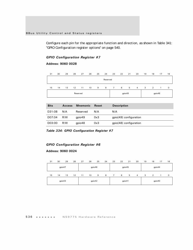
BBus U t i l i t y Con t r o l a nd S t a t u s r e g i s t e r s
5 3 6 NS9775 Ha r dwa r e Re f e r ence
Configure each pin for the appropriate function and direction, as shown in Table 341: "GPIO Configuration register options" on page 540.
GPIO Configuration Register #7
Address: 9060 0028
GPIO Configuration Register #6
Address: 9060 0024
Bits Access Mnemonic Reset Description
D31:08 N/A Reserved N/A N/A
D07:04 R/W gpio49 0x3 gpio[49] configuration
D03:00 R/W gpio48 0x3 gpio[48] configuration
Table 334: GPIO Configuration Register #7
gpio49
13 12 11 10 9 8 7 6 5 4 3 2 1 015 14
31 29 28 27 26 25 24 23 22 21 20 19 18 17 1630
Reserved
Reserved gpio48
gpio41
13 12 11 10 9 8 7 6 5 4 3 2 1 015 14
31 29 28 27 26 25 24 23 22 21 20 19 18 17 1630
gpio40
gpio47 gpio46 gpio45 gpio44
gpio43 gpio42
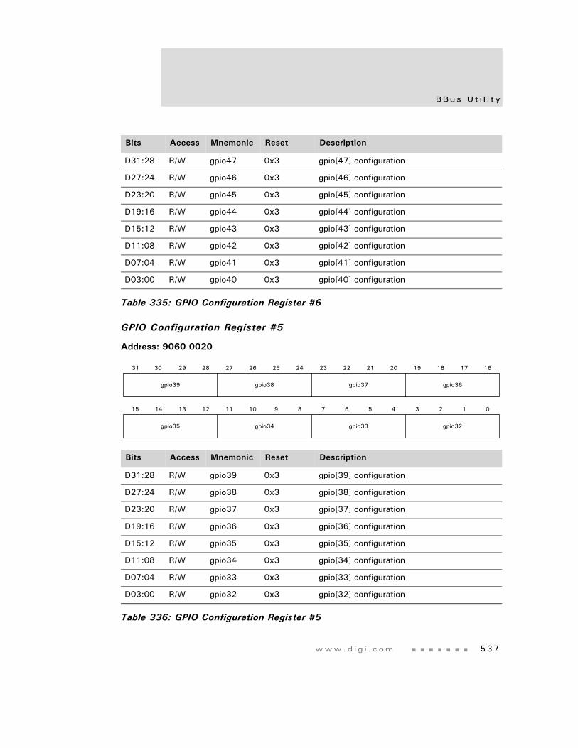
www.d i g i . com 537
BBus U t i l i t y
GPIO Configuration Register #5
Address: 9060 0020
Bits Access Mnemonic Reset Description
D31:28 R/W gpio47 0x3 gpio[47] configuration
D27:24 R/W gpio46 0x3 gpio[46] configuration
D23:20 R/W gpio45 0x3 gpio[45] configuration
D19:16 R/W gpio44 0x3 gpio[44] configuration
D15:12 R/W gpio43 0x3 gpio[43] configuration
D11:08 R/W gpio42 0x3 gpio[42] configuration
D07:04 R/W gpio41 0x3 gpio[41] configuration
D03:00 R/W gpio40 0x3 gpio[40] configuration
Table 335: GPIO Configuration Register #6
Bits Access Mnemonic Reset Description
D31:28 R/W gpio39 0x3 gpio[39] configuration
D27:24 R/W gpio38 0x3 gpio[38] configuration
D23:20 R/W gpio37 0x3 gpio[37] configuration
D19:16 R/W gpio36 0x3 gpio[36] configuration
D15:12 R/W gpio35 0x3 gpio[35] configuration
D11:08 R/W gpio34 0x3 gpio[34] configuration
D07:04 R/W gpio33 0x3 gpio[33] configuration
D03:00 R/W gpio32 0x3 gpio[32] configuration
Table 336: GPIO Configuration Register #5
gpio33
13 12 11 10 9 8 7 6 5 4 3 2 1 015 14
31 29 28 27 26 25 24 23 22 21 20 19 18 17 1630
gpio32
gpio39 gpio38 gpio37 gpio36
gpio35 gpio34
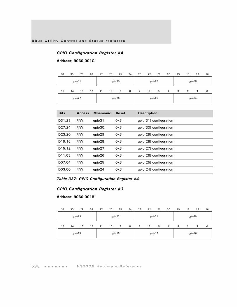
BBus U t i l i t y Con t r o l a nd S t a t u s r e g i s t e r s
5 3 8 NS9775 Ha r dwa r e Re f e r ence
GPIO Configuration Register #4
Address: 9060 001C
GPIO Configuration Register #3
Address: 9060 0018
Bits Access Mnemonic Reset Description
D31:28 R/W gpio31 0x3 gpio[31] configuration
D27:24 R/W gpio30 0x3 gpio[30] configuration
D23:20 R/W gpio29 0x3 gpio[29] configuration
D19:16 R/W gpio28 0x3 gpio[28] configuration
D15:12 R/W gpio27 0x3 gpio[27] configuration
D11:08 R/W gpio26 0x3 gpio[26] configuration
D07:04 R/W gpio25 0x3 gpio[25] configuration
D03:00 R/W gpio24 0x3 gpio[24] configuration
Table 337: GPIO Configuration Register #4
gpio25
13 12 11 10 9 8 7 6 5 4 3 2 1 015 14
31 29 28 27 26 25 24 23 22 21 20 19 18 17 1630
gpio24
gpio31 gpio30 gpio29 gpio28
gpio27 gpio26
gpio17
13 12 11 10 9 8 7 6 5 4 3 2 1 015 14
31 29 28 27 26 25 24 23 22 21 20 19 18 17 1630
gpio16
gpio23 gpio22 gpio21 gpio20
gpio19 gpio18

www.d i g i . com 539
BBus U t i l i t y
GPIO Configuration Register #2
Address: 9060 0014
Bits Access Mnemonic Reset Description
D31:28 R/W gpio23 0x3 gpio[23] configuration
D27:24 R/W gpio22 0x3 gpio[22] configuration
D23:20 R/W gpio21 0x3 gpio[21] configuration
D19:16 R/W gpio20 0x3 gpio[20] configuration
D15:12 R/W gpio19 0x3 gpio[19] configuration
D11:08 R/W gpio18 0x3 gpio[18] configuration
D07:04 R/W gpio17 0x3 gpio[17] configuration
D03:00 R/W gpio16 0x3 gpio[16] configuration
Table 338: GPIO Configuration register #3
Bits Access Mnemonic Reset Description
D31:28 R/W gpio15 0x3 gpio[15] configuration
D27:24 R/W gpio14 0x3 gpio[14] configuration
D23:20 R/W gpio13 0x3 gpio[13] configuration
D19:16 R/W gpio12 0x3 gpio[12] configuration
D15:12 R/W gpio11 0x3 gpio[11] configuration
D11:08 R/W gpio10 0x3 gpio[10] configuration
D07:04 R/W gpio9 0x3 gpio[9] configuration
D03:00 R/W gpio8 0x3 gpio[8] configuration
Table 339: GPIO Configuration Register #2
gpio9
13 12 11 10 9 8 7 6 5 4 3 2 1 015 14
31 29 28 27 26 25 24 23 22 21 20 19 18 17 1630
gpio8
gpio15 gpio14 gpio13 gpio12
gpio11 gpio10
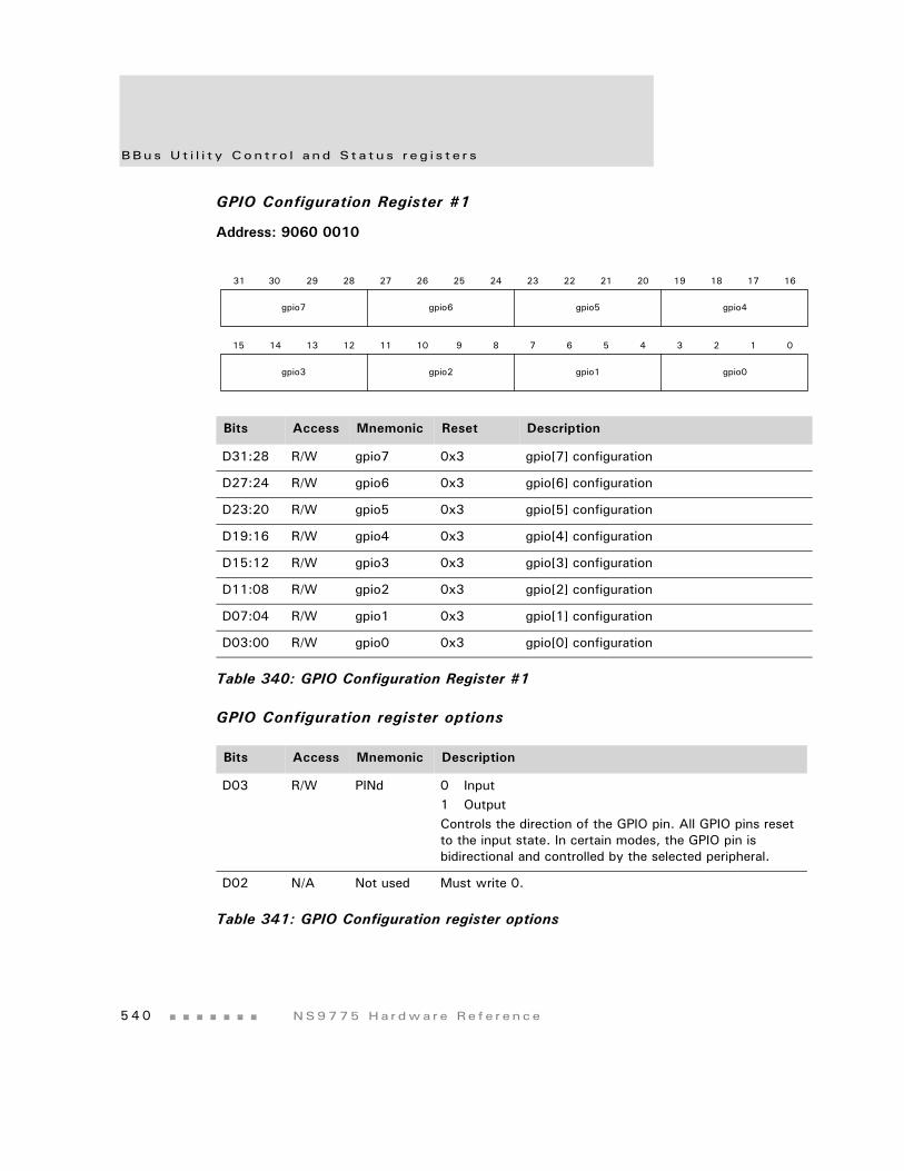
BBus U t i l i t y Con t r o l a nd S t a t u s r e g i s t e r s
5 4 0 NS9775 Ha r dwa r e Re f e r ence
GPIO Configuration Register #1
Address: 9060 0010
GPIO Configuration register options
Bits Access Mnemonic Reset Description
D31:28 R/W gpio7 0x3 gpio[7] configuration
D27:24 R/W gpio6 0x3 gpio[6] configuration
D23:20 R/W gpio5 0x3 gpio[5] configuration
D19:16 R/W gpio4 0x3 gpio[4] configuration
D15:12 R/W gpio3 0x3 gpio[3] configuration
D11:08 R/W gpio2 0x3 gpio[2] configuration
D07:04 R/W gpio1 0x3 gpio[1] configuration
D03:00 R/W gpio0 0x3 gpio[0] configuration
Table 340: GPIO Configuration Register #1
Bits Access Mnemonic Description
D03 R/W PINd 0 Input1 OutputControls the direction of the GPIO pin. All GPIO pins reset to the input state. In certain modes, the GPIO pin is bidirectional and controlled by the selected peripheral.
D02 N/A Not used Must write 0.
Table 341: GPIO Configuration register options
gpio1
13 12 11 10 9 8 7 6 5 4 3 2 1 015 14
31 29 28 27 26 25 24 23 22 21 20 19 18 17 1630
gpio7 gpio6 gpio5 gpio4
gpio3 gpio2 gpio0
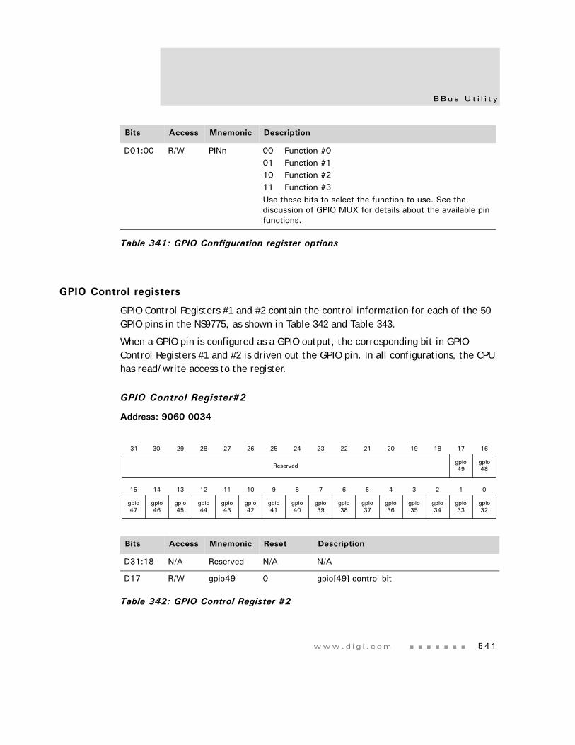
www.d i g i . com 541
BBus U t i l i t y
GPIO Control registers
GPIO Control Registers #1 and #2 contain the control information for each of the 50 GPIO pins in the NS9775, as shown in Table 342 and Table 343.
When a GPIO pin is configured as a GPIO output, the corresponding bit in GPIO Control Registers #1 and #2 is driven out the GPIO pin. In all configurations, the CPU has read/write access to the register.
GPIO Control Register#2
Address: 9060 0034
D01:00 R/W PINn 00 Function #001 Function #110 Function #211 Function #3Use these bits to select the function to use. See the discussion of GPIO MUX for details about the available pin functions.
Bits Access Mnemonic Description
Table 341: GPIO Configuration register options
Bits Access Mnemonic Reset Description
D31:18 N/A Reserved N/A N/A
D17 R/W gpio49 0 gpio[49] control bit
Table 342: GPIO Control Register #2
13 12 11 10 9 8 7 6 5 4 3 2 1 015 14
31 29 28 27 26 25 24 23 22 21 20 19 18 17 1630
gpio49Reserved
gpio48
gpio47
gpio46
gpio45
gpio44
gpio43
gpio42
gpio41
gpio40
gpio39
gpio38
gpio37
gpio36
gpio35
gpio34
gpio33
gpio32
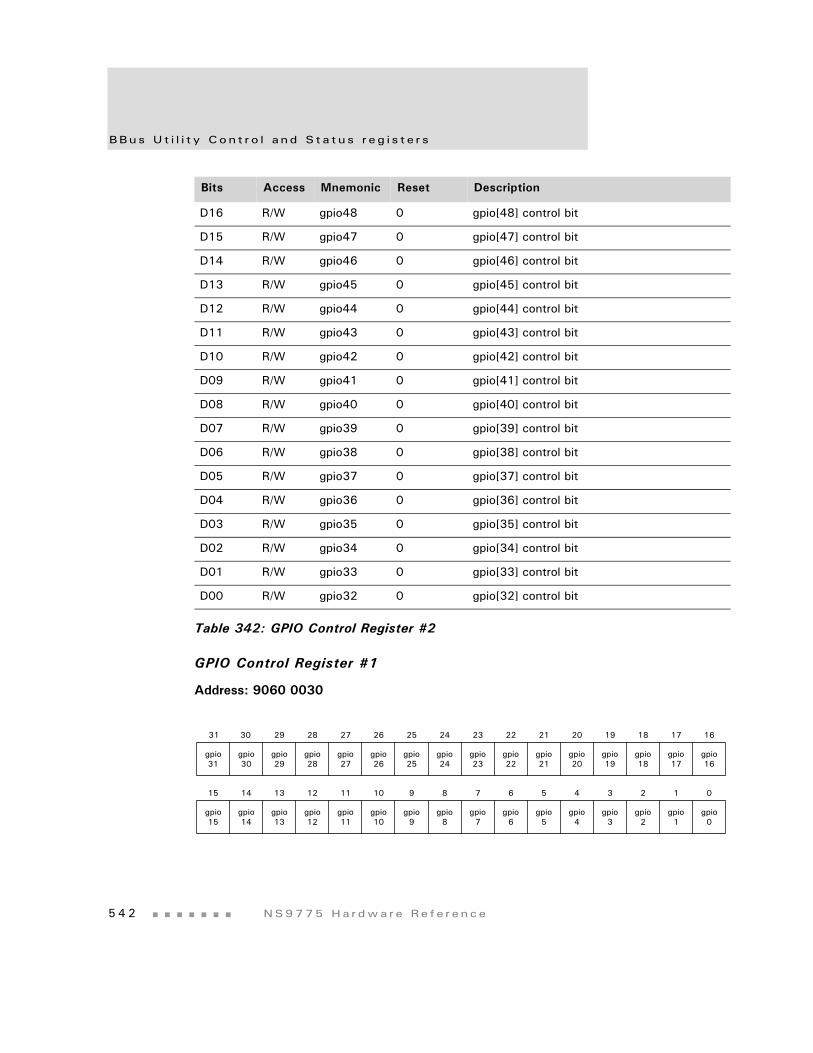
BBus U t i l i t y Con t r o l a nd S t a t u s r e g i s t e r s
5 4 2 NS9775 Ha r dwa r e Re f e r ence
GPIO Control Register #1
Address: 9060 0030
D16 R/W gpio48 0 gpio[48] control bit
D15 R/W gpio47 0 gpio[47] control bit
D14 R/W gpio46 0 gpio[46] control bit
D13 R/W gpio45 0 gpio[45] control bit
D12 R/W gpio44 0 gpio[44] control bit
D11 R/W gpio43 0 gpio[43] control bit
D10 R/W gpio42 0 gpio[42] control bit
D09 R/W gpio41 0 gpio[41] control bit
D08 R/W gpio40 0 gpio[40] control bit
D07 R/W gpio39 0 gpio[39] control bit
D06 R/W gpio38 0 gpio[38] control bit
D05 R/W gpio37 0 gpio[37] control bit
D04 R/W gpio36 0 gpio[36] control bit
D03 R/W gpio35 0 gpio[35] control bit
D02 R/W gpio34 0 gpio[34] control bit
D01 R/W gpio33 0 gpio[33] control bit
D00 R/W gpio32 0 gpio[32] control bit
Bits Access Mnemonic Reset Description
Table 342: GPIO Control Register #2
13 12 11 10 9 8 7 6 5 4 3 2 1 015 14
31 29 28 27 26 25 24 23 22 21 20 19 18 17 1630
gpio17
gpio16
gpio15
gpio14
gpio13
gpio12
gpio11
gpio10
gpio9
gpio8
gpio7
gpio6
gpio5
gpio4
gpio3
gpio2
gpio1
gpio0
gpio31
gpio30
gpio29
gpio28
gpio27
gpio26
gpio25
gpio24
gpio23
gpio22
gpio21
gpio20
gpio19
gpio18
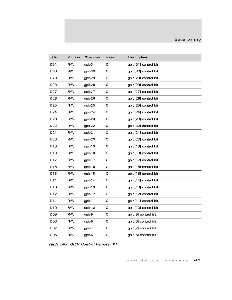
www.d i g i . com 543
BBus U t i l i t y
Bits Access Mnemonic Reset Description
D31 R/W gpio31 0 gpio[31] control bit
D30 R/W gpio30 0 gpio[30] control bit
D29 R/W gpio29 0 gpio[29] control bit
D28 R/W gpio28 0 gpio[28] control bit
D27 R/W gpio27 0 gpio[27] control bit
D26 R/W gpio26 0 gpio[26] control bit
D25 R/W gpio25 0 gpio[25] control bit
D24 R/W gpio24 0 gpio[24] control bit
D23 R/W gpio23 0 gpio[23] control bit
D22 R/W gpio22 0 gpio[22] control bit
D21 R/W gpio21 0 gpio[21] control bit
D20 R/W gpio20 0 gpio[20] control bit
D19 R/W gpio19 0 gpio[19] control bit
D18 R/W gpio18 0 gpio[18] control bit
D17 R/W gpio17 0 gpio[17] control bit
D16 R/W gpio16 0 gpio[16] control bit
D15 R/W gpio15 0 gpio[15] control bit
D14 R/W gpio14 0 gpio[14] control bit
D13 R/W gpio13 0 gpio[13] control bit
D12 R/W gpio12 0 gpio[12] control bit
D11 R/W gpio11 0 gpio[11] control bit
D10 R/W gpio10 0 gpio[10] control bit
D09 R/W gpio9 0 gpio[9] control bit
D08 R/W gpio8 0 gpio[8] control bit
D07 R/W gpio7 0 gpio[7] control bit
D06 R/W gpio6 0 gpio[6] control bit
Table 343: GPIO Control Register #1
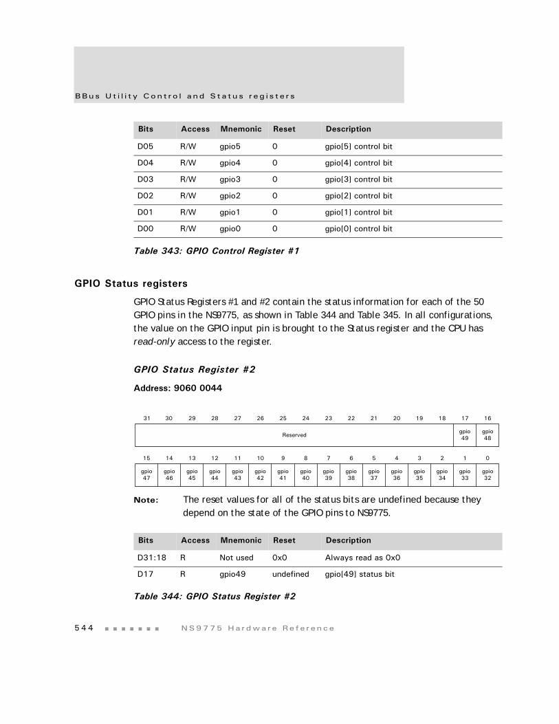
BBus U t i l i t y Con t r o l a nd S t a t u s r e g i s t e r s
5 4 4 NS9775 Ha r dwa r e Re f e r ence
GPIO Status registers
GPIO Status Registers #1 and #2 contain the status information for each of the 50 GPIO pins in the NS9775, as shown in Table 344 and Table 345. In all configurations, the value on the GPIO input pin is brought to the Status register and the CPU hasread-only access to the register.
GPIO Status Register #2
Address: 9060 0044
Note: The reset values for all of the status bits are undefined because they depend on the state of the GPIO pins to NS9775.
D05 R/W gpio5 0 gpio[5] control bit
D04 R/W gpio4 0 gpio[4] control bit
D03 R/W gpio3 0 gpio[3] control bit
D02 R/W gpio2 0 gpio[2] control bit
D01 R/W gpio1 0 gpio[1] control bit
D00 R/W gpio0 0 gpio[0] control bit
Bits Access Mnemonic Reset Description
Table 343: GPIO Control Register #1
Bits Access Mnemonic Reset Description
D31:18 R Not used 0x0 Always read as 0x0
D17 R gpio49 undefined gpio[49] status bit
Table 344: GPIO Status Register #2
13 12 11 10 9 8 7 6 5 4 3 2 1 015 14
31 29 28 27 26 25 24 23 22 21 20 19 18 17 1630
gpio49Reserved
gpio48
gpio47
gpio46
gpio45
gpio44
gpio43
gpio42
gpio41
gpio40
gpio39
gpio38
gpio37
gpio36
gpio35
gpio34
gpio33
gpio32
www.d i g i . com 545
BBus U t i l i t y
GPIO Status Register #1
Address: 9060 0040
D16 R gpio48 undefined gpio[48] status bit
D15 R gpio47 undefined gpio[47] status bit
D14 R gpio46 undefined gpio[46] status bit
D13 R gpio45 undefined gpio[45] status bit
D12 R gpio44 undefined gpio[44] status bit
D11 R gpio43 undefined gpio[43] status bit
D10 R gpio42 undefined gpio[42] status bit
D09 R gpio41 undefined gpio[41] status bit
D08 R gpio40 undefined gpio[40] status bit
D07 R gpio39 undefined gpio[39] status bit
D06 R gpio38 undefined gpio[38] status bit
D05 R gpio37 undefined gpio[37] status bit
D04 R gpio36 undefined gpio[36] status bit
D03 R gpio35 undefined gpio[35] status bit
D02 R gpio34 undefined gpio[34] status bit
D01 R gpio33 undefined gpio[33] status bit
D00 R gpio32 undefined gpio[32] status bit
Bits Access Mnemonic Reset Description
Table 344: GPIO Status Register #2
13 12 11 10 9 8 7 6 5 4 3 2 1 015 14
31 29 28 27 26 25 24 23 22 21 20 19 18 17 1630
gpio17
gpio16
gpio15
gpio14
gpio13
gpio12
gpio11
gpio10
gpio9
gpio8
gpio7
gpio6
gpio5
gpio4
gpio3
gpio2
gpio1
gpio0
gpio31
gpio30
gpio29
gpio28
gpio27
gpio26
gpio25
gpio24
gpio23
gpio22
gpio21
gpio20
gpio19
gpio18
BBus U t i l i t y Con t r o l a nd S t a t u s r e g i s t e r s
5 4 6 NS9775 Ha r dwa r e Re f e r ence
Note: The reset values for all of the status bits are undefined because they depend on the state of the GPIO pins to NS9775.
Bits Access Mnemonic Reset Description
D31 R gpio31 undefined gpio[31] status bit
D30 R gpio30 undefined gpio[30] status bit
D29 R gpio29 undefined gpio[29] status bit
D28 R gpio28 undefined gpio[28] status bit
D27 R gpio27 undefined gpio[27] status bit
D26 R gpio26 undefined gpio[26] status bit
D25 R gpio25 undefined gpio[25] status bit
D24 R gpio24 undefined gpio[24] status bit
D23 R gpio23 undefined gpio[23] status bit
D22 R gpio22 undefined gpio[22] status bit
D21 R gpio21 undefined gpio[21] status bit
D20 R gpio20 undefined gpio[20] status bit
D19 R gpio19 undefined gpio[19] status bit
D18 R gpio18 undefined gpio[18] status bit
D17 R gpio17 undefined gpio[17] status bit
D16 R gpio16 undefined gpio[16] status bit
D15 R gpio15 undefined gpio[15] status bit
D14 R gpio14 undefined gpio[14] status bit
D13 R gpio13 undefined gpio[13] status bit
D12 R gpio12 undefined gpio[12] status bit
D11 R gpio11 undefined gpio[11] status bit
D10 R gpio10 undefined gpio[10] status bit
D09 R gpio9 undefined gpio[9] status bit
D08 R gpio8 undefined gpio[8] status bit
D07 R gpio7 undefined gpio[7] status bit
Table 345: GPIO Status Register #1
www.d i g i . com 547
BBus U t i l i t y
BBus Monitor register
Address: 9060 0050Write 0 to this register.
D06 R gpio6 undefined gpio[6] status bit
D05 R gpio5 undefined gpio[5] status bit
D04 R gpio4 undefined gpio[4] status bit
D03 R gpio3 undefined gpio[3] status bit
D02 R gpio2 undefined gpio[2] status bit
D01 R gpio1 undefined gpio[1] status bit
D00 R gpio0 undefined gpio[0] status bit
Bits Access Mnemonic Reset Description
Table 345: GPIO Status Register #1
13 12 11 10 9 8 7 6 5 4 3 2 1 015 14
31 29 28 27 26 25 24 23 22 21 20 19 18 17 1630
Not used
Not used
BBus U t i l i t y Con t r o l a nd S t a t u s r e g i s t e r s
5 4 8 NS9775 Ha r dwa r e Re f e r ence
BBus DMA Interrupt Status register
Address: 9060 0060The BBus DMA Interrupt Status register contains the interrupt status bits for the BBus DMA Controller. The interrupt bits are active high. Service these interrupts in the BBus DMA controller.
Register bit assignment
Bits Access Mnemonic Reset Description
D31:16 R Not used 0x0 Always read as 0x0
D15 R BINT16 0 BBus DMA channel #16 interrupt status
D14 R BINT15 0 BBus DMA channel #15 interrupt status
D13 R BINT14 0 BBus DMA channel #14 interrupt status
D12 R BINT13 0 BBus DMA channel #13 interrupt status
D11 R BINT12 0 BBus DMA channel #12 interrupt status
D10 R BINT11 0 BBus DMA channel #11 interrupt status
D09 R BINT10 0 BBus DMA channel #10 interrupt status
D08 R BINT9 0 BBus DMA channel #9 interrupt status
D07 R BINT8 0 BBus DMA channel #8 interrupt status
D06 R BINT7 0 BBus DMA channel #7 interrupt status
D05 R BINT6 0 BBus DMA channel #6 interrupt status
D04 R BINT5 0 BBus DMA channel #5 interrupt status
D03 R BINT4 0 BBus DMA channel #4 interrupt status
Table 346: BBus DMA Interrupt Status register
BINT14
13 12 11 10 9 8 7 6 5 4 3 2 1 015 14
31 29 28 27 26 25 24 23 22 21 20 19 18 17 1630
Not used
BINT16
BINT15
BINT13
BINT12
BINT11
BINT10
BINT9
BINT8
BINT7
BINT6
BINT5
BINT4
BINT3
BINT2
BINT1
www.d i g i . com 549
BBus U t i l i t y
BBus DMA Interrupt Enable register
Address: 9060 0064The BBus DMA Interrupt Enable register allows you to enable or disable the BBus DMA interrupts on an individual basis. Writing a 1 enables the interrupt.
Register bit assignment
D02 R BINT3 0 BBus DMA channel #3 interrupt status
D01 R BINT2 0 BBus DMA channel #2 interrupt status
D00 R BINT1 0 BBus DMA channel #1 interrupt status
Bits Access Mnemonic Reset Description
Table 346: BBus DMA Interrupt Status register
Bits Access Mnemonic Reset Description
D31:16 R Not used 0x0 Always read as 0x0
D15 R/W BINT_EN16 0 BBus DMA channel #16 interrupt enable
D14 R/W BINT_EN15 0 BBus DMA channel #15 interrupt enable
D13 R/W BINT_EN14 0 BBus DMA channel #14 interrupt enable
D12 R/W BINT_EN13 0 BBus DMA channel #13 interrupt enable
D11 R/W BINT_EN12 0 BBus DMA channel #12 interrupt enable
D10 R/W BINT_EN11 0 BBus DMA channel #11 interrupt enable
D09 R/W BINT_EN10 0 BBus DMA channel #10 interrupt enable
D08 R/W BINT_EN9 0 BBus DMA channel #9 interrupt enable
Table 347: BBus DMA Interrupt Enable register
BINT_EN14
13 12 11 10 9 8 7 6 5 4 3 2 1 015 14
31 29 28 27 26 25 24 23 22 21 20 19 18 17 1630
Not used
BINT_EN16
BINT_EN15
BINT_EN13
BINT_EN12
BINT_EN11
BINT_EN10
BINT_EN9
BINT_EN8
BINT_EN7
BINT_EN6
BINT_EN5
BINT_EN4
BINT_EN3
BINT_EN2
BINT_EN1
BBus U t i l i t y Con t r o l a nd S t a t u s r e g i s t e r s
5 5 0 NS9775 Ha r dwa r e Re f e r ence
USB Configuration register
Address: 9060 0070The USB Configuration register contains power-on USB configuration information. Write to this register only when the USB module is in reset, as indicated by the USB field in the Master Reset register (see page 535).
Register bit assignment
D07 R/W BINT_EN8 0 BBus DMA channel #8 interrupt enable
D06 R/W BINT_EN7 0 BBus DMA channel #7 interrupt enable
D05 R/W BINT_EN6 0 BBus DMA channel #6 interrupt enable
D04 R/W BINT_EN5 0 BBus DMA channel #5 interrupt enable
D03 R/W BINT_EN4 0 BBus DMA channel #4 interrupt enable
D02 R/W BINT_EN3 0 BBus DMA channel #3 interrupt enable
D01 R/W BINT_EN2 0 BBus DMA channel #2 interrupt enable
D00 R/W BINT_EN1 0 BBus DMA channel #1 interrupt enable
Bits Access Mnemonic Reset Description
Table 347: BBus DMA Interrupt Enable register
Bits Access Mnemonic Reset Description
D31:04 R Not used 0x0 Always read as 0x0
Table 348: USB Configuration register
13 12 11 10 9 8 7 6 5 4 3 2 1 015 14
31 29 28 27 26 25 24 23 22 21 20 19 18 17 1630
Not used
Not used OUTEN SPEED CFG
www.d i g i . com 551
BBus U t i l i t y
Endian Configuration register
Address: 9060 0080The Endian Configuration register contains the endian control for the BBus peripherals and the AHB bus master. NS9775 can be configured such that some peripherals transfer data in direct mode and some peripherals transfer data in DMA mode. Those that are accessed in direct mode must have their endian configuration match the AHB. The endian configuration of the AHB master must always match the AHB.
D03 R/W OUTEN 0 Enables the USB output driver during USB loopback testing. The output driver is enabled only when either the host or device indicates that it is driving the USB pins. Writing a 1 enables this feature.
D02 R/W SPEED 1 0 Low speed (1.5 Mbps)1 Full speed (12 Mbps)Defines the operational speed of the USB device block.
D01:00 R/W CFG 11 Configuration00 USB disabled01 USB device mode; no software control10 USB host mode; no software control11 USB device mode; software control
enabledDefines the operational mode of the USB module. This field can be modified only when the USB field in the Master Reset register is asserted (see page 535). For normal operation, this field should not need to be modified.
Bits Access Mnemonic Reset Description
Table 348: USB Configuration register
BBus U t i l i t y Con t r o l a nd S t a t u s r e g i s t e r s
5 5 2 NS9775 Ha r dwa r e Re f e r ence
Register bit assignment
Bits Access Mnemonic Reset Description
D31:13 R Not used 0x0 Always read as 0x0
D12 R/W AHBM Reset to the value provided on strapping pin gpio[44]
AHB bus master0 Little endian1 Big endian
D11:08 N/A Reserved N/A N/A
D07 R/W I2C 0 I2C controller0 Little endian1 Big endian
D06 R/W IEEE1284 0 IEEE 1284 controller0 Little endian1 Big endian
D05 R/W SerD 0 Serial controller port D0 Little endian1 Big endian
D04 R/W SerC 0 Serial controller port C0 Little endian1 Big endian
D03 R/W SerA 0 Serial controller port A0 Little endian1 Big endian
Table 349: Endian Configuration register
13 12 11 10 9 8 7 6 5 4 3 2 1 015 14
31 29 28 27 26 25 24 23 22 21 20 19 18 17 1630
Not used
Not used AHBM Reserved I2C IEEE1284 SerD SerC SerA SerB USB DMA
www.d i g i . com 553
BBus U t i l i t y
ARM Wake-up register
Address: 9060 0090The ARM Wake-up register contains the ARM wake-up word used only by Serial Controller Interface #1. This pattern, when found as the next entry in the receive FIFO, causes a wake-up signal to be asserted to the ARM.
Register bit assignment
D02 R/W SerB 0 Serial controller port B0 Little endian1 Big endian
D01 R/W USB 0 USB0 Little endian1 Big endianThis does not affect the USB DMA controller.
D00 R/W DMA Reset to the value provided on strapping pin gpio[44]
BBus DMA0 Little endian1 Big endianThis field controls both the general BBus DMA controller and the USB DMA controller.
Bits Access Mnemonic Reset Description
Table 349: Endian Configuration register
Bits Access Mnemonic Reset Description
D31:00 R/W WAKE 0x0000_0000 Defines the byte-wise match in order for the Serial Controller to signal a wake-up to the ARM.
Table 350: ARM Wake-up register
13 12 11 10 9 8 7 6 5 4 3 2 1 015 14
31 29 28 27 26 25 24 23 22 21 20 19 18 17 1630
WAKE
WAKE

555
I2C Master/Slave InterfaceC H A P T E R 1 1
The I2C master/slave interface provides an interface between the ARM CPU and the I2C bus.
The I2C master/slave interface basically is a parallel-to-serial and serial-to-parallel converter. The parallel data received from the ARM CPU has to be converted to an appropriate serial form to be transmitted to an external component using the I2C bus. Similarly, the serial data received from the I2C bus has to be converted to an appropriate parallel form for the ARM CPU. The I2C master interface also manages the interface timing, data structure, and error handling.
Ove r v i ew
5 5 6 NS9775 Ha r dwa r e Re f e r ence
Overview
The I2C module is designed to be a master and slave. The slave is active only when the module is being addressed during an I2C bus transfer; the master can arbitrate for and access the I2C bus only when the bus is free (idle) — therefore, the master and slave are mutually exclusive.
Physical I2C bus
The physical I2C bus consists of two open-drain signal lines: serial data (SDA) and serial clock (SCL). Pullup resistors are required; see the standard I2C bus specification for the correct value for the application. Each device connected to the bus is software-addressable by a unique 7- or 10-bit address, and a simple master/slave relationship exists at all times.
A master can operate as a master-transmitter (writes)) or a master-receiver (reads). The slaves respond to the received commands accordingly:
In transmit mode (slave is read), the host interface receives character-based parallel data from the ARM. The module converts the parallel data to serial format and transmits the serial data to the I2C bus.
In receive mode (slave is written to), the I2C bus interface receives 8-bit-based serial data from the I2C bus. The module converts the serial data to parallel format and interrupts the host. The host’s interrupt service routine reads the parallel data from the data register inside the I2C module. The serial data stream synchronization and throttling are done by modulating the serial clock. Serial clock modulation can be controlled by both the transmitter and receiver, based in their hosts’ service speed.
The I2C is a true multi-master bus with collision detection and arbitration to prevent data corruption when two or more masters initiate transfer simultaneously. If a master loses arbitration during the addressing stage, it is possible that the winning master is trying to address the transfer. The losing master must therefore immediately switch over to its slave mode.
The on-chip filtering rejects spikes on the bus data line to preserve data integrity. The number of ICs that can be connected to the same bus is limited only by a maximum bus capacity of 400 pf.
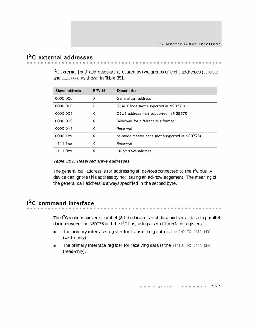
www.d i g i . com 557
I2C Mas t e r / S l a ve I n t e r f a c e
I2C external addresses
I2C external [bus] addresses are allocated as two groups of eight addresses (0000XXX and 1111XXX), as shown in Table 351.
The general call address is for addressing all devices connected to the I2C bus. A device can ignore this address by not issuing an acknowledgement. The meaning of the general call address is always specified in the second byte.
I2C command interface
The I2C module converts parallel (8-bit) data to serial data and serial data to parallel data between the NS9775 and the I2C bus, using a set of interface registers.
The primary interface register for transmitting data is the CMD_TX_DATA_REG (write-only).
The primary interface register for receiving data is the STATUS_RX_DATA_REG (read-only).
Slave address R/W bit Description
0000 000 0 General call address
0000 000 1 START byte (not supported in NS9775)
0000 001 X CBUS address (not supported in NS9775)
0000 010 X Reserved for different bus format
0000 011 X Reserved
0000 1xx X hs-mode master code (not supported in NS9775)
1111 1xx X Reserved
1111 0xx X 10-bit slave address
Table 351: Reserved slave addresses
I 2C command i n t e r f a c e
5 5 8 NS9775 Ha r dwa r e Re f e r ence
Locked interrupt driven mode
I2C operates in a locked interrupt driven mode, which means that each command issued must wait for an interrupt response before the next command can be issued (illustrated in "Flow charts," beginning on page 568).
The first bit of the command — 0 or 1 — indicates to which module — master or slave, respectively — the command in the CMD field (of the CMD_TX_DATA_REG; see page 560) is sent. The master module can be sent a master command only; the slave module can be sent a slave command only (see "Master and slave module commands," beginning on page 558, for a list of commands). If a command is sent to the master module, that module is locked until a command acknowledgement is given. Similarly, if a command is sent to the slave module, the slave module is locked until it receives a command acknowledgement. With either module, the acknowledgement can be any interrupt associated with that module. When a module is locked, another command must not be sent to that module.
The command lock status can be checked in the STATUS_RX_DATA_REG.
Master module and slave module commands
The I2C master recognizes four high-level commands, which are used in the CMD field of the Command register (see page 560); the I2C slave recognizes two high-level commands:
Command Name Description
00hex M_NOP No operation.
04hex M_READ Start reading bytes from slave.
05hex M_WRITE Start writing bytes to slave.
06hex M_STOP Stop this transaction (give up the I2C bus).
10hex S_NOP No operation. This command is necessary for 16-bit mode, providing data in TX_DATA_REG without a command.
16hex S_STOP Stop transaction by not acknowledging the byte received.
Table 352: Master and slave module commands
www.d i g i . com 559
I2C Mas t e r / S l a ve I n t e r f a c e
Bus arbitration
Any M_READ or M_WRITE command causes the I2C module to participate in the bus arbitration process when the I2C bus is free (idle). If the module becomes the new bus owner, the transaction goes through. If the module loses bus arbitration, an M_ARBIT_LOST interrupt is generated to the host processor and the command must be reissued.
I2C registers
All registers have 8-bit definitions, but must be accessed in pairs. For example, TX_DATA_REG and CMD_REG are written simultaneously and RX_DATA_REG and STATUS_REG are read simultaneously.
Table 353 shows the register addresses.
After a reset, all registers are set to the initial value. If an unspecified register or bit is read, a zero is returned.
Register Description
9050 0000 Command Transmit Data register (CMD_TX_DATA_REG)Status Receive Data register (STATUS_RX_DATA_REG)
9050 0004 Master Address register
9050 0008 Slave Address register
9050 000C Configuration register
Table 353: I2C register address map
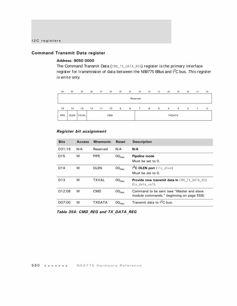
I 2C r e g i s t e r s
5 6 0 NS9775 Ha r dwa r e Re f e r ence
Command Transmit Data register
Address: 9050 0000The Command Transmit Data (CMD_TX_DATA_REG) register is the primary interface register for transmission of data between the NS9775 BBus and I2C bus. This register is write only.
Register bit assignment
Bits Access Mnemonic Reset Description
D31:16 N/A Reserved N/A N/A
D15 W PIPE 00hex Pipeline modeMust be set to 0.
D14 W DLEN 00hex I2C DLEN port (iic_dlen)Must be set to 0.
D13 W TXVAL 00hex Provide new transmit data in CMD_TX_DATA_REG (tx_data_val).
D12:08 W CMD 00hex Command to be sent (see "Master and slave module commands," beginning on page 558)
D07:00 W TXDATA 00hex Transmit data to I2C bus.
Table 354: CMD_REG and TX_DATA_REG
TXVAL CMD TXDATA
13 12 11 10 9 8 7 6 5 4 3 2 1 015 14
PIPE DLEN
31 29 28 27 26 25 24 23 22 21 20 19 18 17 1630
Reserved
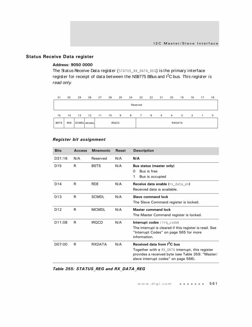
www.d i g i . com 561
I2C Mas t e r / S l a ve I n t e r f a c e
Status Receive Data register
Address: 9050 0000The Status Receive Data register (STATUS_RX_DATA_REG) is the primary interface register for receipt of data between the NS9775 BBus and I2C bus. This register is read only.
Register bit assignment
Bits Access Mnemonic Reset Description
D31:16 N/A Reserved N/A N/A
D15 R BSTS N/A Bus status (master only)0 Bus is free1 Bus is occupied
D14 R RDE N/A Receive data enable (rx_data_en)Received data is available.
D13 R SCMDL N/A Slave command lockThe Slave Command register is locked.
D12 R MCMDL N/A Master command lockThe Master Command register is locked.
D11:08 R IRQCD N/A Interrupt codes (irq_code)The interrupt is cleared if this register is read. See "Interrupt Codes" on page 565 for more information.
D07:00 R RXDATA N/A Received data from I2C busTogether with a RX_DATA interrupt, this register provides a received byte (see Table 359: "Master/slave interrupt codes" on page 566).
Table 355: STATUS_REG and RX_DATA_REG
SCMDL MCMDL IRQCD RXDATA
13 12 11 10 9 8 7 6 5 4 3 2 1 015 14
BSTS RDE
31 29 28 27 26 25 24 23 22 21 20 19 18 17 1630
Reserved
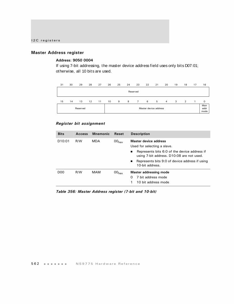
I 2C r e g i s t e r s
5 6 2 NS9775 Ha r dwa r e Re f e r ence
Master Address register
Address: 9050 0004If using 7-bit addressing, the master device address field uses only bits D07:01; otherwise, all 10 bits are used.
Register bit assignment
Bits Access Mnemonic Reset Description
D10:01 R/W MDA 00hex Master device addressUsed for selecting a slave.
Represents bits 6:0 of the device address if using 7-bit address. D10:08 are not used.
Represents bits 9:0 of device address if using 10-bit address.
D00 R/W MAM 00hex Master addressing mode0 7 bit address mode1 10 bit address mode
Table 356: Master Address register (7-bit and 10-bit)
13 12 11 10 9 8 7 6 5 4 3 2 1 015 14
31 29 28 27 26 25 24 23 22 21 20 19 18 17 1630
Reserved
Master device addressMstraddrmode
Reserved
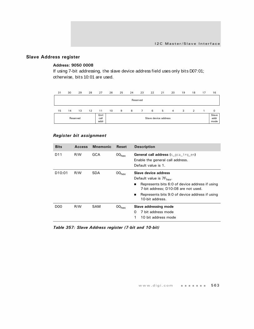
www.d i g i . com 563
I2C Mas t e r / S l a ve I n t e r f a c e
Slave Address register
Address: 9050 0008If using 7-bit addressing, the slave device address field uses only bits D07:01; otherwise, bits 10:01 are used.
Register bit assignment
Bits Access Mnemonic Reset Description
D11 R/W GCA 00hex General call address (s_gca_irq_en)Enable the general call address. Default value is 1.
D10:01 R/W SDA 00hex Slave device addressDefault value is 7Fhex.
Represents bits 6:0 of device address if using 7-bit address; D10:08 are not used.
Represents bits 9:0 of device address if using 10-bit address.
D00 R/W SAM 00hex Slave addressing mode0 7 bit address mode1 10 bit address mode
Table 357: Slave Address register (7-bit and 10-bit)
13 12 11 10 9 8 7 6 5 4 3 2 1 015 14
31 29 28 27 26 25 24 23 22 21 20 19 18 17 1630
Reserved
Slave device addressSlaveaddrmode
ReservedGnrlcalladdr
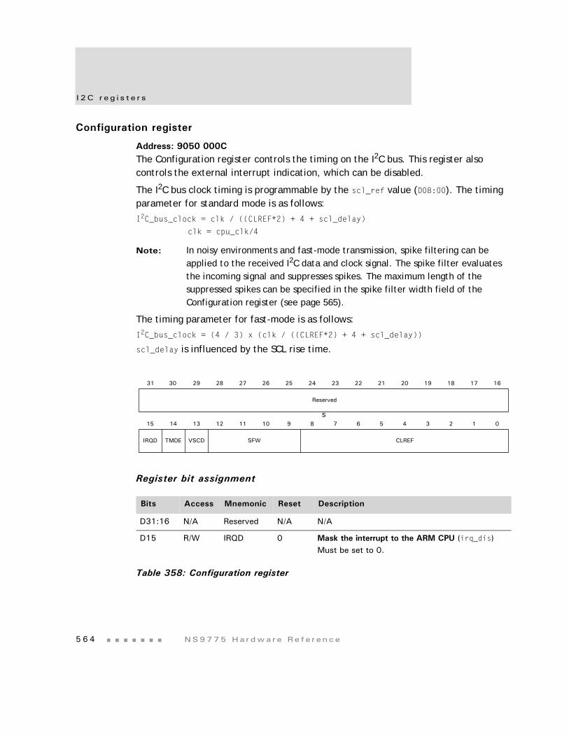
I 2C r e g i s t e r s
5 6 4 NS9775 Ha r dwa r e Re f e r ence
Configuration register
Address: 9050 000CThe Configuration register controls the timing on the I2C bus. This register also controls the external interrupt indication, which can be disabled.
The I2C bus clock timing is programmable by the scl_ref value (D08:00). The timing parameter for standard mode is as follows:
I2C_bus_clock = clk / ((CLREF*2) + 4 + scl_delay)
clk = cpu_clk/4
Note: In noisy environments and fast-mode transmission, spike filtering can be applied to the received I2C data and clock signal. The spike filter evaluates the incoming signal and suppresses spikes. The maximum length of the suppressed spikes can be specified in the spike filter width field of the Configuration register (see page 565).
The timing parameter for fast-mode is as follows:
I2C_bus_clock = (4 / 3) x (clk / ((CLREF*2) + 4 + scl_delay))
scl_delay is influenced by the SCL rise time.
Register bit assignment
Bits Access Mnemonic Reset Description
D31:16 N/A Reserved N/A N/A
D15 R/W IRQD 0 Mask the interrupt to the ARM CPU (irq_dis)Must be set to 0.
Table 358: Configuration register
13 12 11 10 9 8 7 6 5 4 3 2 1 015 14
31 29 28 27 26 25 24 23 22 21 20 19 18 17 1630
Reserved
CLREFIRQD TMDE VSCD SFW
s
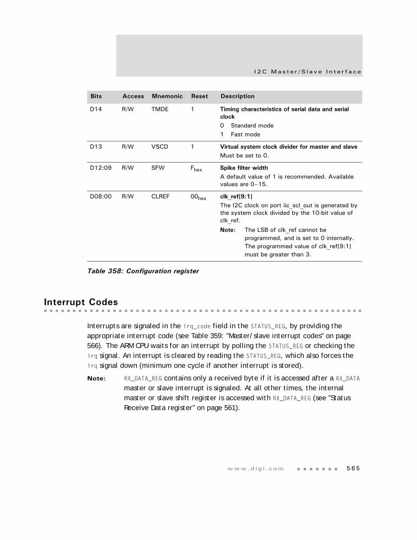
www.d i g i . com 565
I2C Mas t e r / S l a ve I n t e r f a c e
Interrupt Codes
Interrupts are signaled in the irq_code field in the STATUS_REG, by providing the appropriate interrupt code (see Table 359: "Master/slave interrupt codes" on page 566). The ARM CPU waits for an interrupt by polling the STATUS_REG or checking the irq signal. An interrupt is cleared by reading the STATUS_REG, which also forces the irq signal down (minimum one cycle if another interrupt is stored).
Note: RX_DATA_REG contains only a received byte if it is accessed after a RX_DATA master or slave interrupt is signaled. At all other times, the internal master or slave shift register is accessed with RX_DATA_REG (see "Status Receive Data register" on page 561).
D14 R/W TMDE 1 Timing characteristics of serial data and serial clock0 Standard mode1 Fast mode
D13 R/W VSCD 1 Virtual system clock divider for master and slaveMust be set to 0.
D12:09 R/W SFW Fhex Spike filter widthA default value of 1 is recommended. Available values are 0–15.
D08:00 R/W CLREF 00hex clk_ref[9:1]The I2C clock on port iic_scl_out is generated by the system clock divided by the 10-bit value of clk_ref.
Note: The LSB of clk_ref cannot be programmed, and is set to 0 internally. The programmed value of clk_ref[9:1] must be greater than 3.
Bits Access Mnemonic Reset Description
Table 358: Configuration register
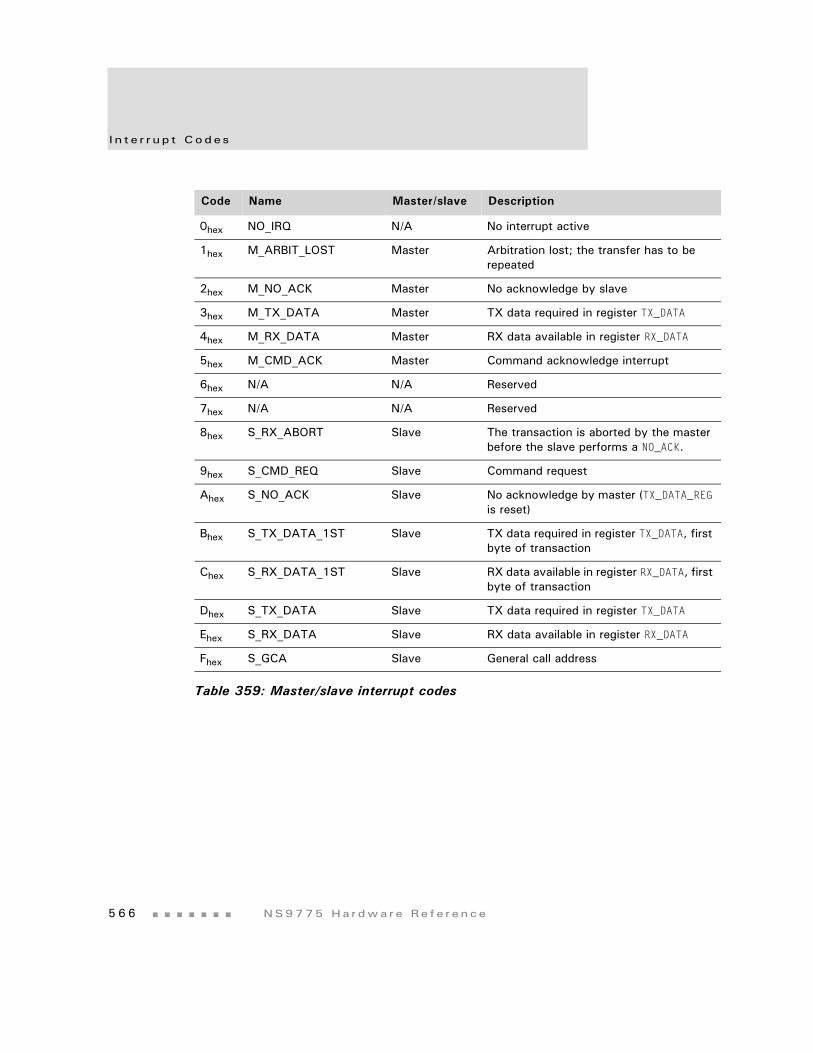
I n t e r r u p t Codes
5 6 6 NS9775 Ha r dwa r e Re f e r ence
Code Name Master/slave Description
0hex NO_IRQ N/A No interrupt active
1hex M_ARBIT_LOST Master Arbitration lost; the transfer has to be repeated
2hex M_NO_ACK Master No acknowledge by slave
3hex M_TX_DATA Master TX data required in register TX_DATA
4hex M_RX_DATA Master RX data available in register RX_DATA
5hex M_CMD_ACK Master Command acknowledge interrupt
6hex N/A N/A Reserved
7hex N/A N/A Reserved
8hex S_RX_ABORT Slave The transaction is aborted by the master before the slave performs a NO_ACK.
9hex S_CMD_REQ Slave Command request
Ahex S_NO_ACK Slave No acknowledge by master (TX_DATA_REG is reset)
Bhex S_TX_DATA_1ST Slave TX data required in register TX_DATA, first byte of transaction
Chex S_RX_DATA_1ST Slave RX data available in register RX_DATA, first byte of transaction
Dhex S_TX_DATA Slave TX data required in register TX_DATA
Ehex S_RX_DATA Slave RX data available in register RX_DATA
Fhex S_GCA Slave General call address
Table 359: Master/slave interrupt codes
www.d i g i . com 567
I2C Mas t e r / S l a ve I n t e r f a c e
Software driver
The I2C master software driver uses three commands only:
M_READ to start a read sequence
M_WRITE to start a write sequence
M_STOP to give up the I2C bus
If, during a read or write sequence, another M_READ or M_WRITE is requested by the ARM CPU, a restart is performed on the I2C bus. This opens the opportunity to provide a new slave device address in the MAster Address register before the command request.
The I2C slave high level driver identifies one command: S_STOP, to discontinue a transaction. After this command, the slave remains inactive until the next start condition on the I2C bus. If a slave is accessed by a master, it generates S_RX_DATA and S_TX_DATA interrupts (see "Master/slave interrupt codes" on page 566). To distinguish the transactions from each other, special S_RX_DATA_1ST and S_TX_DATA_1ST interrupts are generated for the transmitted byte.
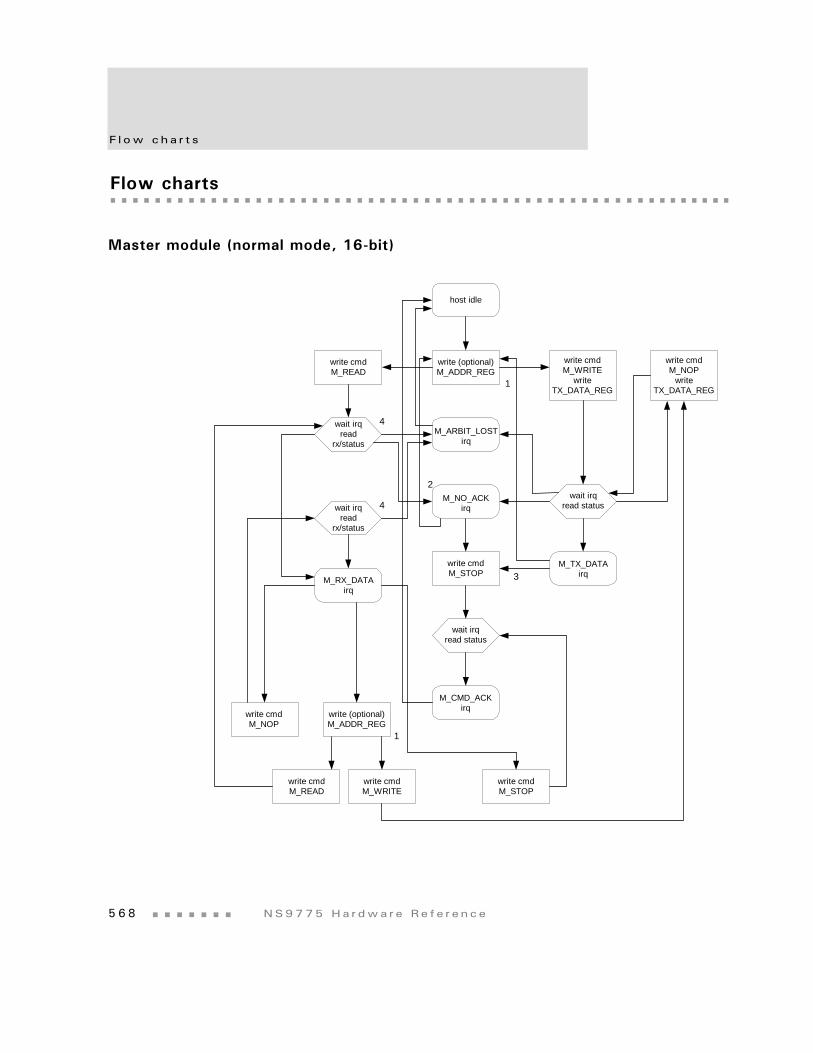
F l ow cha r t s
5 6 8 NS9775 Ha r dwa r e Re f e r ence
Flow charts
Master module (normal mode, 16-bit)
host idle
write (optional)M_ADDR_REG
write cmdM_READ
wait irqread
rx/status
wait irqread
rx/status
M_RX_DATAirq
M_ARBIT_LOSTirq
M_NO_ACKirq
write cmdM_STOP
wait irqread status
M_CMD_ACKirq
write cmdM_WRITE
writeTX_DATA_REG
write cmdM_NOP
writeTX_DATA_REG
wait irqread status
M_TX_DATAirq
write cmdM_NOP
write cmdM_STOP
4
4
2
3
1
write cmdM_WRITE
write (optional)M_ADDR_REG
write cmdM_READ
1
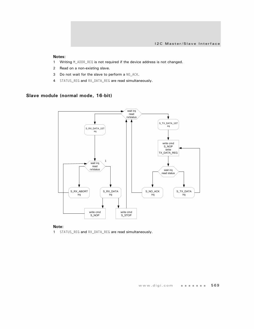
www.d i g i . com 569
I2C Mas t e r / S l a ve I n t e r f a c e
Notes:1 Writing M_ADDR_REQ is not required if the device address is not changed.
2 Read on a non-existing slave.
3 Do not wait for the slave to perform a NO_ACK.
4 STATUS_REG and RX_DATA_REG are read simultaneously.
Slave module (normal mode, 16-bit)
Note:1 STATUS_REG and RX_DATA_REG are read simultaneously.
wait irqread
rx/status
S_RX_DATA_1STirq
S_TX_DATA_1STirq
wait irqread
rx/status
1
S_RX_ABORTirq
S_RX_DATAirq
S_NO_ACK irq
S_TX_DATAirq
wait irqread status
write cmdS_NOP
writeTX_DATA_REG
write cmdS_NOP
write cmdS_STOP

571
LCD ControllerC H A P T E R 1 2
The NS9775 LCD (Liquid Crystal Display) controller is a DMA master module that connects to the AHB bus. The LCD controller provides the signals required to interface directly to TFT and STN color and monochrome LCD panels.
LCD controller timing diagrams can be found in the Timing chapter.
LCD f e a t u r e s
5 7 2 NS9775 Ha r dwa r e Re f e r ence
LCD features
The NS9775 LCD controller provides these features:
Dual 64-deep, 32-bit wide FIFOs, for buffering incoming display data
Support for color and monochrome single- and dual-panel for Super Twisted Nematic (STN) displays with 4- or 8-bit interfaces
Support for Thin Film Transistor (TFT) color displays
Resolution programmable up to 1024 x 768
15 gray-level mono, 3375 color STN, and 64K color TFT support
– Patented gray-scale algorithm
1, 2, or 4 bits-per-pixel (bpp) palettized displays for mono STN
1, 2, 4, or 8 bpp palettized color displays for color STN and TFT
16 bpp true-color non-palettized, for color STN and TFT
24 bpp true-color non-palettized for TFT
Programmable timing for different display panels
256 entry, 16-bit palette RAM, arranged as a 128 x 32-bit RAM
Frame, line, and pixel clock signals
AC bias signal for STN, data enable signal for TFT panels
Support for little and big endian, as well as Windows CE data formats
Programmable parameters
These key parameters are programmable:
Horizontal front and back porch
Horizontal synchronization pulse width
Number of pixels per line
Vertical front and back porch
Vertical synchronization pulse width
Number of lines per panel
Number of panel clocks per line
www.d i g i . com 573
LCD Con t r o l l e r
Signal polarity, active high or low
AC panel bias
Panel clock frequency
Bits-per-pixel
Display type, STN mono/color or TFT
STN 4- or 8-bit interface mode
STN dual- or single-panel mode
Little endian, big endian, or WinCE mode
Interrupt generation event
LCD panel resolution
The LCD can be programmed to support a wide range of panel resolutions, including but not limited to:
320 x 200, 320 x 240
640 x 200, 640 x 240, 640 x 480
800 x 600
1024 x 768
LCD panel support
The LCD controller supports these types of panels:
Active matrix TFT panels with up to 24-bit bus interface
Single-panel monochrome STN panels (4-bit and 8-bit bus interface)
Dual-panel monochrome STN panels (4-bit and 8-bit bus interface per panel)
Single-panel color STN panels, 8-bit bus interface
Dual-panel color STN panels, 8-bit bus interface per panel
LCD f e a t u r e s
5 7 4 NS9775 Ha r dwa r e Re f e r ence
Number of colors
The number of colors supported differs per panel type.
TFT panels
TFT panels support one or more of these color modes:
1 bpp, palettized, 2 colors selected from available colors
2 bpp, palettized, 4 colors selected from available colors
4 bpp, palettized, 16 colors selected from available colors
8 bpp, palettized, 256 colors selected from available colors
16 bpp, direct 5:5:5 RGB, with one bpp usually not used. This pixel is still output, and can be used as a bright bit to connect to the least significant bit (lsb) of R, G, and B components of a 6:6:6 TFT panel.
24 bpp, direct 8:8:8 RGB, providing over 16 million colors
Each 16-bit palette entry is made up of five bpp (RGB) plus a common intensity bit, which provides better memory use and performance compared with a full six bpp structure. The total amount of colors supported can be doubled from 32K to 64K if the intensity bit is used and applied to all three color components simultaneously.
Color STN panels
Color STN panels support one or more of these color modes:
1 bpp, palettized, 2 colors selected from 3375
2 bpp, palettized, 4 colors selected from 3375
4 bpp, palettized, 16 colors selected from 3375
8 bpp, palettized, 256 colors selected from 3375
16 bpp, direct 4:4:4 RGB, with 4 bpp not used
www.d i g i . com 575
LCD Con t r o l l e r
Mono STN panels
Mono STN panels support one or more of these modes:
1 bpp, palettized, 2 grayscales selected from 15
2 bpp, palettized, 4 grayscales selected from 15
4 bpp, palettized, 15 grayscales selected from 15
LCD power up and power down sequence support
This procedure provides an example of how the LCD controller can be programmed to provide the powerup sequence to an LCD panel (see Figure 88, "Power up and power down sequences," on page 576):
1 VDD is applied simultaneously to the NS9775 and panel display driver logic. The following signals are pulled up to VDD until the LCD controller is configured: CLLP, CLCP, CLFP, CLAC, CLD[23:0], and CLLE.
2 After the LCD controller is configured, a 1 is written to the LcdEn bit in the LCDControl register. This enables the CLLP, CLCP, CLFP, CLAC, and CLLE signals, but the CLD[23:0] signals will be low.
3 When the signals in Step 2 have stabilized, the contrast voltage, VEE (which is not controlled or supplied by the LCD controller), is applied where appropriate. If required, a software timer routine can be used to provide the minimum display specific delay time between application of VDD and application of VEE.
4 If required, a software timer routine can be used to provide the minimum display specific delay time between application of the control signals and power to the panel display. When the software timer routine completes, power is applied to the panel by writing a 1 to the LcdPwr bit in the LcdControl register, which, in turn, sets the CLPOWER signal high and enables the CLD[23:0] signals into their active state. The CLPOWER signal gates the power to the LCD panel.
The power down sequence is the reverse of the powerup procedure, with the respective register bits written to 0 rather than 1.
LCD con t r o l l e r f u n c t i o n a l ov e r v i ew
5 7 6 NS9775 Ha r dwa r e Re f e r ence
Figure 88: Power up and power down sequences
LCD controller functional overview
The LCD controller translates pixel-coded data into the required formats and timing to drive a variety of single and dual mono and color LCDs.
The controller supports passive STN and active TFT LCD display types.
STN display panels require algorithmic pixel pattern generation to provide pseudo-grayscaling on mono displays or color creation on color displays.
TFT display panels require the digital color value of each pixel to be applied to the display data units.
Packets of pixel-coded data are fed, through the AHB interface, to two independent,64-deep, 32-bit wide DMA FIFOs, which act as input data flow buffers. The buffered pixel-coded data is then unpacked using a pixel serializer.
LCD on sequence LCD off sequence
Min. 0ms
Min. (display specific) ms(provided through software)
Min. (display specific) ms(provided through software)
Vdd
CLLP, CLCP, CLFPCLAC, CLLE
Vee
CLPOWERCLD[23:0]
Min. (display specific) ms(provided through software)
LcdEn=1LcdPwr=1
LcdEn=0
LcdPwr=0
LCDConfigured
www.d i g i . com 577
LCD Con t r o l l e r
Depending on the LCD type and mode, the unpacked data can represent one of the following:
An actual true display gray or color value
An address to a 256 x 16 bit wide palette RAM gray or color value
With STN displays, either a value obtained from the addressed palette location or the true value is passed to the grayscaling generators. The hardware-coded grayscale algorithm logic sequences the addressed pixels activity over a programmed number of frames to provide the proper display appearance.
With TFT displays, either an addressed palette value or true color value is passed directly to the output display drivers, bypassing the grayscaling algorithm logic.
Clocks
The NS9775 LCD controller requires separate AHB (HCLK) and LCD (CLCDCLK) input clocks. The source of CLCDCLK is programmable using the LCD panel select field in the Clock Configuration register. Table 360 shows the clock selections.
The LCD controller uses CLCDCLK internally. The clock sent to the LCD panel (CLCP) normally is derived from CLCDCLK using the PCD (panel clock divisor) value in the LCDTiming2 register (see page 598). The LCD controller also can bypass the internal clock divider controlled by PCD and use CLCDCLK as CLCP directly by setting the BCD (bypass pixel clock divider) bit to 1 in the LCDTiming2 register (see page 596).
LCD panel clock select CLCDCLK
000 HCLK
001 HCLK/2
010 HCLK/4
011 HCLK/8
1xx lcdclk/2
Note: lcdclk is an external clock input to NS9775. A divided-by-2 version of this value is sent to the LCD controller.
Table 360: CLCDCLK selection
LCD con t r o l l e r f u n c t i o n a l ov e r v i ew
5 7 8 NS9775 Ha r dwa r e Re f e r ence
Signals and interrupts
The LCD controller provides a set of programmable display control signals, and generates individual interrupts for different conditions.
Programmable control signals
LCD power panel enable
Pixel clock
Horizontal and vertical synchronization pulses
Display bias
Individual interrupts
Base address update signification
Vertical compare
Bus error
There is also a single combined interrupt that is generated when any of the individual interrupts become active.
Figure 89 shows the LCD controller module.
www.d i g i . com 579
LCD Con t r o l l e r
Figure 89: LCD controller block diagram
AHB slave interface Timing controller Panel clockgenerator
AHB masterinterface
DMA FIFOcontroller
Pixelserializer
Upperhalf-word
Lowerhalf-word
Greyscaler
Register/paletteprogramming LCD panel
control signals
LCD panelclock
UpperpanelFIFO
LowerpanelFIFO
Frame bufferaccess
Bit 0
Palette RAM external
Palette
TRUECOLOR
Upper panelformatter
Lower panelformatter
LCD panel data
TFTTFT paneldata
AHB i n t e r f a c e
5 8 0 NS9775 Ha r dwa r e Re f e r ence
AHB interface
The AHB interface includes the AHB slave interface and the AHB master interface.
AHB master and slave interfaces
The AHB master interface transfers display data from memory to the LCD controller DMA FIFOs.
The AHB slave interface connects the LCD to the AHB bus and provides CPU accesses to the registers and palette RAM. The LCD controller AHB slave interface supports these features:
Dual DMA FIFOs and associated control logic
The pixel data accessed from memory is buffered by two DMA FIFOs, which can be controlled independently to cover single and dual panel LCD types. Each FIFO is 64 words deep by 32 bits wide, and can be cascaded to form a 128-word deep FIFO in single panel mode. The FIFO input ports are connected to the AHB interface and the output port feeds the pixel serializer.
Synchronization logic is used to transfer the pixel data from the AHB HCLK domain to the CLCDCLK clock domain. The DMA FIFOs are clocked by HCLK.
The water level marks within each FIFO are set such that each FIFO requests data when at least four locations become available.
www.d i g i . com 581
LCD Con t r o l l e r
Pixel serializer
The pixel serializer block reads the 32-bit wide LCD data from DMA FIFO output port, and extracts 24, 16, 8, 4, 2, or 1 bpp, depending on the current mode of operation. The LCD controller supports big endian, little endian, and WinCE data formats. In dual panel mode, data is read alternately from the upper and lower DMA FIFOs. The mode of operation determines whether the extracted data is used to point to a color/grayscale value in the palette ram or is actually a true color value that can be applied directly to an LCD panel input.
The next six figures show the data structure in each DMA FIFO word corresponding to the Endianness and bpp combinations. For each of the three supported data formats, the required data for each panel display pixel must be extracted from the data word.
Figure 90 and Figure 91 show the data structure for little endian byte, little endian pixel — LBLP.
Figure 92 and Figure 93 show the data structure for big endian byte, big endian pixel — BBBP.
Figure 94 and Figure 95 show the data structure for little endian byte, big endian pixel — LBBP. (This is WinCE format.)

AHB i n t e r f a c e
5 8 2 NS9775 Ha r dwa r e Re f e r ence
Figure 90: LBLP, DMA FIFO output bits 31:16
Figure 91: LBLP, DMA FIFO output bits 15:0
DMA FIFO OUTPUT BITS
bpp
1
2
4
8
16
24
1 0 1 0 1 0 1 0 1 0 1 0 1 0 1 0
3 2 1 0 3 2 1 0 3 2 1 0 3 2 1 0
7 6 5 4 3 2 1 0 7 6 5 4 3 2 1 0
31 30 29 28 27 26 25 24 23 22 21 20 19 18 17 16
15 14 13 12 11 10 9 8 7 6 5 4 3 2 1 0
23 22 21 20 19 18 17 16
p31 p30 p29 p28 p27 p26 p25 p24 p23 p22 p21 p20 p19 p18 p17 p16
p15 p14 p13 p12 p11 p10 p9 p8
p7 p6 p5 p4
p3 p2
p1
p0
DMA FIFO OUTPUT BITS
bpp
1
2
4
8
16
24
1 0 1 0 1 0 1 0 1 0 1 0 1 0 1 0
3 2 1 0 3 2 1 0 3 2 1 0 3 2 1 0
7 6 5 4 3 2 1 0 7 6 5 4 3 2 1 0
15 14 13 12 11 10 9 8 7 6 5 4 3 2 1 0
15 14 13 12 11 10 9 8 7 6 5 4 3 2 1 0
7 6 5 4 3 2 1 0
p15 p14 p13 p12 p11 p10 p9 p8 p7 p6 p5 p4 p3 p2 p1 p0
p7 p6 p5 p4 p3 p2 p1 p0
p3 p2 p1 p0
p1 p0
p0
p0
15 14 13 12 11 10 9 8
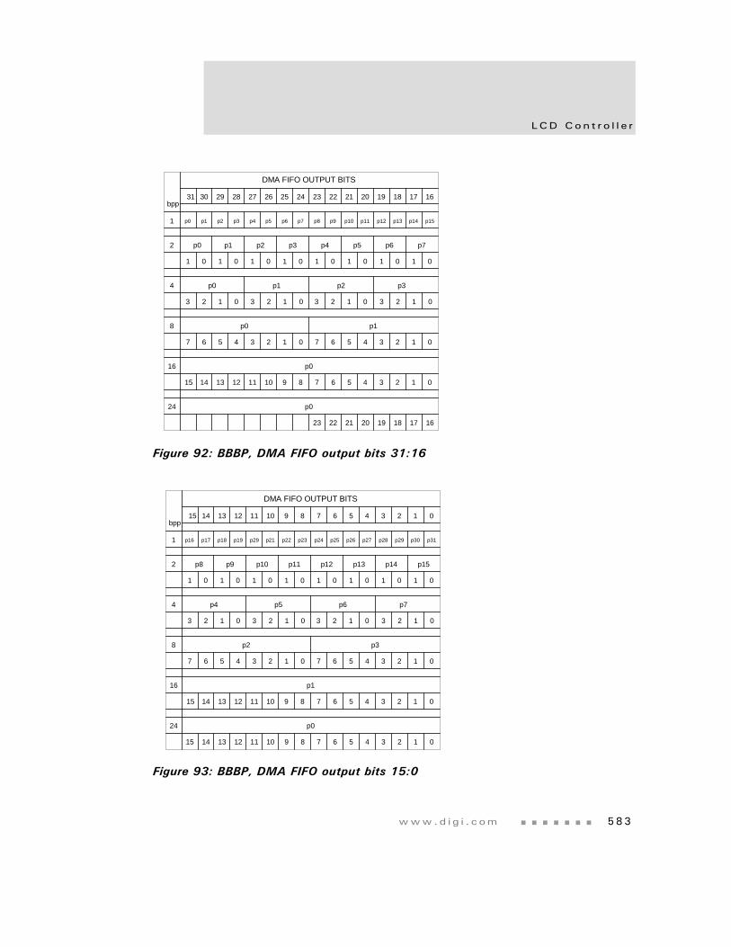
www.d i g i . com 583
LCD Con t r o l l e r
Figure 92: BBBP, DMA FIFO output bits 31:16
Figure 93: BBBP, DMA FIFO output bits 15:0
DMA FIFO OUTPUT BITS
bpp
1
2
4
8
16
24
1 0 1 0 1 0 1 0 1 0 1 0 1 0 1 0
3 2 1 0 3 2 1 0 3 2 1 0 3 2 1 0
7 6 5 4 3 2 1 0 7 6 5 4 3 2 1 0
31 30 29 28 27 26 25 24 23 22 21 20 19 18 17 16
15 14 13 12 11 10 9 8 7 6 5 4 3 2 1 0
23 22 21 20 19 18 17 16
p0 p1 p2 p3 p4 p5 p6 p7 p8 p9 p10 p11 p12 p13 p14 p15
p0 p1 p2 p3 p4 p5 p6 p7
p0 p1 p2 p3
p0 p1
p0
p0
DMA FIFO OUTPUT BITS
bpp
1
2
4
8
16
24
1 0 1 0 1 0 1 0 1 0 1 0 1 0 1 0
3 2 1 0 3 2 1 0 3 2 1 0 3 2 1 0
7 6 5 4 3 2 1 0 7 6 5 4 3 2 1 0
15 14 13 12 11 10 9 8 7 6 5 4 3 2 1 0
15 14 13 12 11 10 9 8 7 6 5 4 3 2 1 0
7 6 5 4 3 2 1 0
p16 p17 p18 p19 p29 p21 p22 p23 p24 p25 p26 p27 p28 p29 p30 p31
p8 p9 p10 p11 p12 p13 p14 p15
p4 p5 p6 p7
p2 p3
p1
p0
15 14 13 12 11 10 9 8
AHB i n t e r f a c e
5 8 4 NS9775 Ha r dwa r e Re f e r ence
Figure 94: LBBP, DMA FIFO output bits 31:16
Figure 95: LBBP, DMA FIFO output bits 15:0
DMA FIFO OUTPUT BITS
bpp
1
2
4
8
16
24
1 0 1 0 1 0 1 0 1 0 1 0 1 0 1 0
3 2 1 0 3 2 1 0 3 2 1 0 3 2 1 0
7 6 5 4 3 2 1 0 7 6 5 4 3 2 1 0
31 30 29 28 27 26 25 24 23 22 21 20 19 18 17 16
15 14 13 12 11 10 9 8 7 6 5 4 3 2 1 0
23 22 21 20 19 18 17 16
p24 p25 p26 p27 p28 p29 p30 p31 p16 p17 p18 p19 p20 p21 p22 p23
p12 p13 p14 p15 p8 p9 p10 p11
p6 p7 p4 p5
p3 p2
p1
p0
DMA FIFO OUTPUT BITS
bpp
1
2
4
8
16
24
1 0 1 0 1 0 1 0 1 0 1 0 1 0 1 0
3 2 1 0 3 2 1 0 3 2 1 0 3 2 1 0
7 6 5 4 3 2 1 0 7 6 5 4 3 2 1 0
15 14 13 12 11 10 9 8 7 6 5 4 3 2 1 0
15 14 13 12 11 10 9 8 7 6 5 4 3 2 1 0
7 6 5 4 3 2 1 0
p8 p9 p10 p11 p12 p13 p14 p15 p0 p1 p2 p3 p4 p5 p6 p7
p4 p5 p6 p7 p0 p1 p2 p3
p2 p3 p0 p1
p1 p0
p0
p0
15 14 13 12 11 10 9 8
www.d i g i . com 585
LCD Con t r o l l e r
RAM palette
The palette RAM is a 256 x 16 bit dual port RAM, physically structured as 128 x 32 bit. This allows two entries to be written into the palette from a single word write access. The least significant bit of the serialized pixel data selects between upper and lower halves of the palette RAM. The half selected depends on the byte-ordering mode. In little endian mode, setting the least significant bit selects the upper half of the palette; in big endian mode, setting the least significant bit selects the lower half. Because WinCE byte ordering is little endian, setting the least significant byte results in selection of the upper half of the palette.
Pixel data values can be written and verified using the slave interface.
The palette RAM has independent controls and addresses for each port.
Port1 is used as a read/write port, and is connected to the AHB slave interface. The palette entries can be written and verified through this port.
Port2 is used as a read-only port, and is connected to the unpacker and grayscaler.
Table 361 shows the bit representation of each word in the palette.
For mono STN, only the red palette field bits (4:1) are used. In STN color mode, however, the green and blue [4:1] are also used.
Red and blue pixel data can be swapped to support BGR data format using the appropriate control register bit.
Bit Name Description
31 I Intensity/unused
30:26 B[4:0] Blue palette data
25:20 G[4:0] Green palette data
19:16 R[4:0] Red palette data
15 I Intensity/unused
14:10 B[4:0] Blue palette data
09:05 G[4:0] Green palette data
04:00 R[4:0] Red palette data
Table 361: Palette data storage
AHB i n t e r f a c e
5 8 6 NS9775 Ha r dwa r e Re f e r ence
In 16- and 24-bpp TFT mode, the palette is bypassed and the pixel serializer output is used as the TFT panel data.
Grayscaler
A unique grayscale algorithm drives mono and color STN panels.
For mono displays, the algorithm provides 15 grayscales.
For STN color displays, the three color components (red, green, and blue) are grayscaled simultaneously, resulting in 3375 (15 x 15 x 15) colors available. The grayscaler transforms each 4-bit gray value into a sequence of activity-per-pixel over several frames, relying somewhat on the display characteristics, to give representation of grayscales and color.
Upper and lower panel formatters
Each formatter consists of three 3-bit (red, green, and blue) shift left registers. Red, green, and blue pixel data bit values from the grayscaler are shifted concurrently into the respective registers. When enough data is available, a byte is constructed by multiplexing the registered data to the correct bit position to satisfy the RGB data pattern of the LCD panel. The byte is transferred to the 3-byte FIFO, which has enough space to store eight color pixels.
Panel clock generator
The panel clock generator block output is the panel clock. This is a divided down version of CLCDCLK, and can be programmed in the range CLCDCLK/2 to CLCDCLK/33 to match the bpp data rate of the LCD panel.
Timing controller
The timing controller block’s primary function is to generate the horizontal and vertical timing panel signals. The timing controller also provides the panel bias/enable signal. Use the AHB slave interface to program these signals in the appropriate registers.
www.d i g i . com 587
LCD Con t r o l l e r
Generating interrupts
The LCD controller has three individually masked interrupts and a single combined interrupt. The single combined interrupt is asserted if any of the combined interrupts are asserted and unmasked.
External pad interface signals
The external pad interface signals are brought out through GPIO.
LCD panel signal multiplexing details
The CLLP, CLAC, CLFP, and CLLE signals are common, but the CLD[23:0] bus has eight modes of operation:
TFT 24-bit interface
TFT 18-bit interface
Color STN single panel
Color STN dual panel
4-bit mono STN single panel
4-bit mono STN dual panel
8-bit mono STN single panel
8-bit mono STN dual panel
Signal name Type Description
CLPOWER Output LCD panel power enable
CLLP Output Line synchronization pulse (STN)/horizontal synchronization pulse (TFT)
CLCP Output LCD panel clock
CLFP Output Frame pulse (STN)/vertical synchronization pulse (TFT)
CLAC Output STN AC bias drive or TFT data enable output
CLD[23:0] Output LCD panel data
CLLE Output Line end signal
Table 362: External pad interface signals
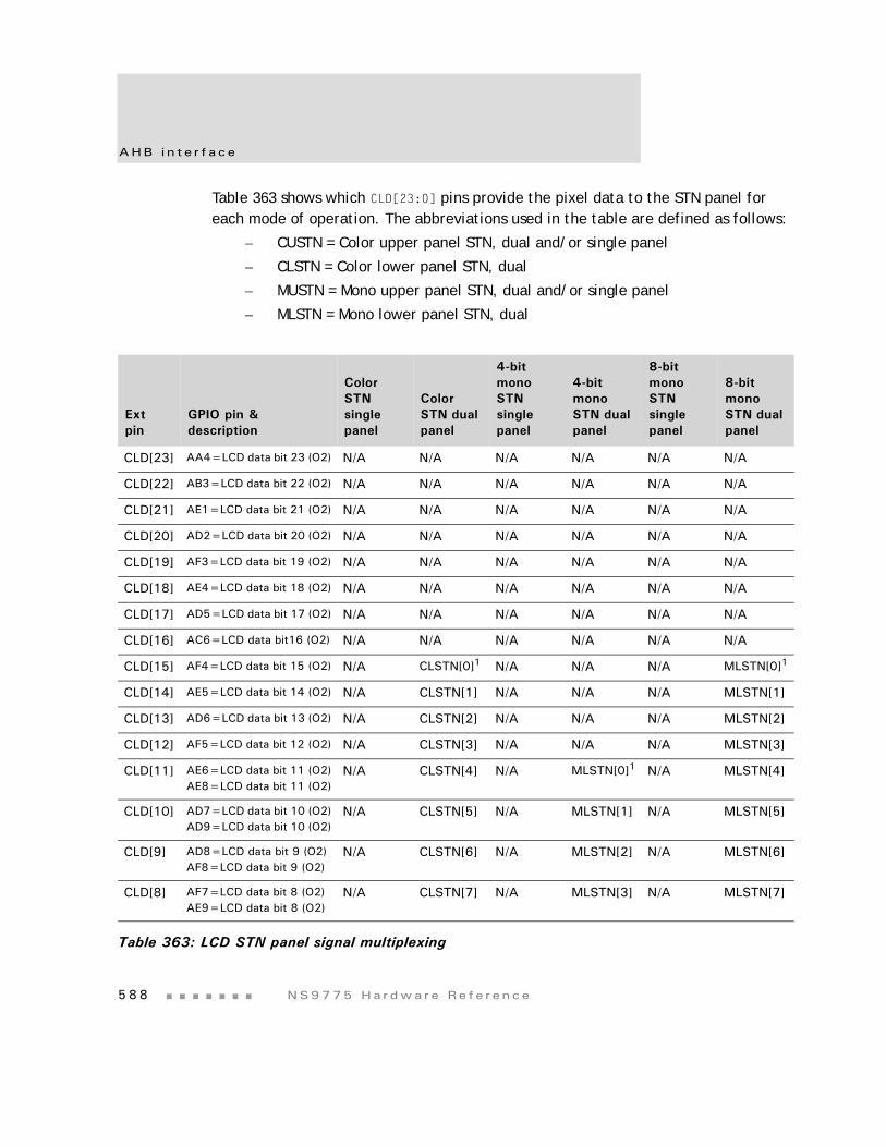
AHB i n t e r f a c e
5 8 8 NS9775 Ha r dwa r e Re f e r ence
Table 363 shows which CLD[23:0] pins provide the pixel data to the STN panel for each mode of operation. The abbreviations used in the table are defined as follows:
– CUSTN = Color upper panel STN, dual and/or single panel
– CLSTN = Color lower panel STN, dual
– MUSTN = Mono upper panel STN, dual and/or single panel
– MLSTN = Mono lower panel STN, dual
Extpin
GPIO pin & description
Color STN single panel
Color STN dual panel
4-bit mono STN single panel
4-bit mono STN dual panel
8-bit mono STN single panel
8-bit mono STN dual panel
CLD[23] AA4=LCD data bit 23 (O2) N/A N/A N/A N/A N/A N/A
CLD[22] AB3=LCD data bit 22 (O2) N/A N/A N/A N/A N/A N/A
CLD[21] AE1=LCD data bit 21 (O2) N/A N/A N/A N/A N/A N/A
CLD[20] AD2=LCD data bit 20 (O2) N/A N/A N/A N/A N/A N/A
CLD[19] AF3=LCD data bit 19 (O2) N/A N/A N/A N/A N/A N/A
CLD[18] AE4=LCD data bit 18 (O2) N/A N/A N/A N/A N/A N/A
CLD[17] AD5=LCD data bit 17 (O2) N/A N/A N/A N/A N/A N/A
CLD[16] AC6=LCD data bit16 (O2) N/A N/A N/A N/A N/A N/A
CLD[15] AF4=LCD data bit 15 (O2) N/A CLSTN[0]1 N/A N/A N/A MLSTN[0]1
CLD[14] AE5=LCD data bit 14 (O2) N/A CLSTN[1] N/A N/A N/A MLSTN[1]
CLD[13] AD6=LCD data bit 13 (O2) N/A CLSTN[2] N/A N/A N/A MLSTN[2]
CLD[12] AF5=LCD data bit 12 (O2) N/A CLSTN[3] N/A N/A N/A MLSTN[3]
CLD[11] AE6=LCD data bit 11 (O2)AE8=LCD data bit 11 (O2)
N/A CLSTN[4] N/A MLSTN[0]1 N/A MLSTN[4]
CLD[10] AD7=LCD data bit 10 (O2)AD9=LCD data bit 10 (O2)
N/A CLSTN[5] N/A MLSTN[1] N/A MLSTN[5]
CLD[9] AD8=LCD data bit 9 (O2)AF8=LCD data bit 9 (O2)
N/A CLSTN[6] N/A MLSTN[2] N/A MLSTN[6]
CLD[8] AF7=LCD data bit 8 (O2)AE9=LCD data bit 8 (O2)
N/A CLSTN[7] N/A MLSTN[3] N/A MLSTN[7]
Table 363: LCD STN panel signal multiplexing
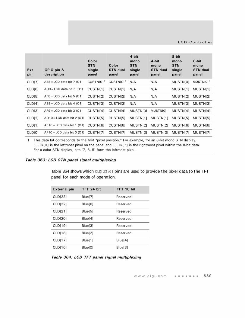
www.d i g i . com 589
LCD Con t r o l l e r
Table 364 shows which CLD[23:0] pins are used to provide the pixel data to the TFT panel for each mode of operation.
CLD[7] AE8=LCD data bit 7 (O1) CUSTN[0]1 CUSTN[0]1 N/A N/A MUSTN[0] MUSTN[0]1
CLD[6] AD9=LCD data bit 6 (O1) CUSTN[1] CUSTN[1] N/A N/A MUSTN[1] MUSTN[1]
CLD[5] AF8=LCD data bit 5 (O1) CUSTN[2] CUSTN[2] N/A N/A MUSTN[2] MUSTN[2]
CLD[4] AE9=LCD data bit 4 (O1) CUSTN[3] CUSTN[3] N/A N/A MUSTN[3] MUSTN[3]
CLD[3] AF9=LCD data bit 3 (O1) CUSTN[4] CUSTN[4] MUSTN[0] MUSTN[0]1 MUSTN[4] MUSTN[4]
CLD[2] AD10=LCD data bit 2 (O1) CUSTN[5] CUSTN[5] MUSTN[1] MUSTN[1] MUSTN[5] MUSTN[5]
CLD[1] AE10=LCD data bit 1 (O1) CUSTN[6] CUSTN[6] MUSTN[2] MUSTN[2] MUSTN[6] MUSTN[6]
CLD[0] AF10=LCD data bit 0 (O1) CUSTN[7] CUSTN[7] MUSTN[3] MUSTN[3] MUSTN[7] MUSTN[7]
1 This data bit corresponds to the first “pixel position.” For example, for an 8-bit mono STN display, CUSTN[0] is the leftmost pixel on the panel and CUSTN[7] is the rightmost pixel within the 8-bit data. For a color STN display, bits [7, 6, 5] form the leftmost pixel.
Extpin
GPIO pin & description
Color STN single panel
Color STN dual panel
4-bit mono STN single panel
4-bit mono STN dual panel
8-bit mono STN single panel
8-bit mono STN dual panel
Table 363: LCD STN panel signal multiplexing
External pin TFT 24 bit TFT 18 bit
CLD[23] Blue[7] Reserved
CLD[22] Blue[6] Reserved
CLD[21] Blue[5] Reserved
CLD[20] Blue[4] Reserved
CLD[19] Blue[3] Reserved
CLD[18] Blue[2] Reserved
CLD[17] Blue[1] Blue[4]
CLD[16] Blue[0] Blue[3]
Table 364: LCD TFT panel signal multiplexing
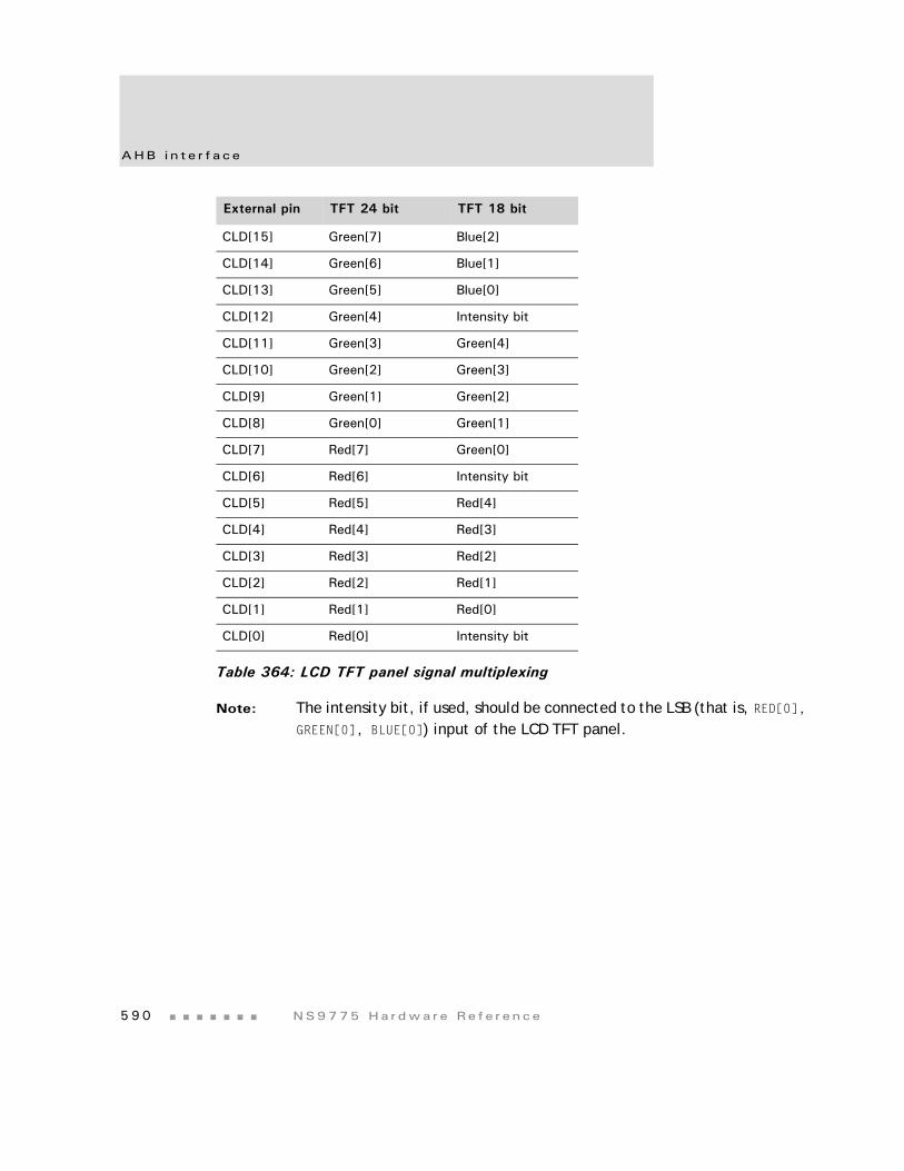
AHB i n t e r f a c e
5 9 0 NS9775 Ha r dwa r e Re f e r ence
Note: The intensity bit, if used, should be connected to the LSB (that is, RED[0], GREEN[0], BLUE[0]) input of the LCD TFT panel.
CLD[15] Green[7] Blue[2]
CLD[14] Green[6] Blue[1]
CLD[13] Green[5] Blue[0]
CLD[12] Green[4] Intensity bit
CLD[11] Green[3] Green[4]
CLD[10] Green[2] Green[3]
CLD[9] Green[1] Green[2]
CLD[8] Green[0] Green[1]
CLD[7] Red[7] Green[0]
CLD[6] Red[6] Intensity bit
CLD[5] Red[5] Red[4]
CLD[4] Red[4] Red[3]
CLD[3] Red[3] Red[2]
CLD[2] Red[2] Red[1]
CLD[1] Red[1] Red[0]
CLD[0] Red[0] Intensity bit
External pin TFT 24 bit TFT 18 bit
Table 364: LCD TFT panel signal multiplexing
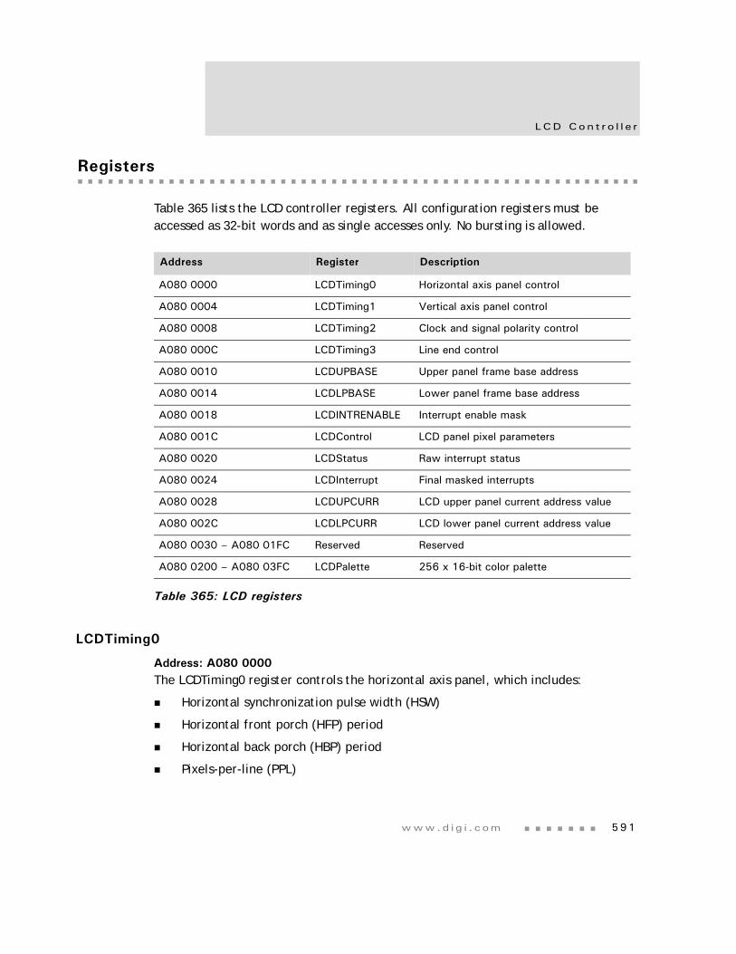
www.d i g i . com 591
LCD Con t r o l l e r
Registers
Table 365 lists the LCD controller registers. All configuration registers must be accessed as 32-bit words and as single accesses only. No bursting is allowed.
LCDTiming0
Address: A080 0000The LCDTiming0 register controls the horizontal axis panel, which includes:
Horizontal synchronization pulse width (HSW)
Horizontal front porch (HFP) period
Horizontal back porch (HBP) period
Pixels-per-line (PPL)
Address Register Description
A080 0000 LCDTiming0 Horizontal axis panel control
A080 0004 LCDTiming1 Vertical axis panel control
A080 0008 LCDTiming2 Clock and signal polarity control
A080 000C LCDTiming3 Line end control
A080 0010 LCDUPBASE Upper panel frame base address
A080 0014 LCDLPBASE Lower panel frame base address
A080 0018 LCDINTRENABLE Interrupt enable mask
A080 001C LCDControl LCD panel pixel parameters
A080 0020 LCDStatus Raw interrupt status
A080 0024 LCDInterrupt Final masked interrupts
A080 0028 LCDUPCURR LCD upper panel current address value
A080 002C LCDLPCURR LCD lower panel current address value
A080 0030 – A080 01FC Reserved Reserved
A080 0200 – A080 03FC LCDPalette 256 x 16-bit color palette
Table 365: LCD registers
Reg i s t e r s
5 9 2 NS9775 Ha r dwa r e Re f e r ence
Register bit assignment
Bits Access Mnemonic Reset Description
D31:24 R/W HBP 0x00 Horizontal back porchNumber of CLCP periods between the negation of CLLP and the start of active data. Program this field with value minus 1.HBP specifies the number of pixel clock periods inserted at the beginning of each line or row of pixels. HBP can generate a delay of 1 to 256 pixel clock cycles.
D23:16 R/W HFP 0x00 Horizontal front porchNumber of CLCP periods between the end of active data and the assertion of CLLP. Program this field with value minus 1. HFP sets the number of pixel clock periods at the end of each line or row of pixels, before CLLP is asserted. HFP can generate a period of 1 to 256 pixel clock cycles.
D15:08 R/W HSW 0x00 Horizontal synchronization pulse widthWidth of the CLLP signal in CLCP periods. Program this field with value minus 1.HSW specifies the pulse width of the line clock in passive mode, or the horizontal synchronization pulse in active mode.
Table 366: LCDTiming0 register
HBP
PPL
13 12 11 10 9 8 7 6 5 4 3 2 1 015 14
31 29 28 27 26 25 24 23 22 21 20 19 18 17 1630
HSW
HFP
Reserved
www.d i g i . com 593
LCD Con t r o l l e r
Horizontal timing restrictions
DMA requests new data at the beginning of a horizontal display line. Some time must be allowed for the DMA transfer and for the data to propagate down the FIFO path in the LCD interface. The data path latency forces some restrictions on the usable minimum values for horizontal porch width in STN mode. The minimum values are HSW = 2 and HBP = 2. Table 367 shows the recommended minimum values for STN displays:
If sufficient time is given at the beginning of the line (for example, HSW is set to 6 and HBP is set to 10), data will not become corrupted for PCD = 4 (minimum value for dual panel mode).
D07:02 R/W PPL 0x00 Pixels-per-lineActual pixels-per-line = 16 * (PPL+1)The PPL field specifies the number of pixels in each line or row of the screen. PPL is a 6-bit value that represents between 16 and 1024 PPL. PPL counts the number of pixel clocks that occur before HFP is applied (program the value required divided by 16, minus 1).
D01:00 N/A Reserved N/A N/A
Mode HSW HBP HFP Panel clock divisor (PCD)
Single panel STN mode 3 5 5 1 (CLCDCLK/3)
Dual panel STN mode 3 5 5 5 (CLCDCLK/7)
Table 367: Minimum recommended values for STN displays
Bits Access Mnemonic Reset Description
Table 366: LCDTiming0 register
Reg i s t e r s
5 9 4 NS9775 Ha r dwa r e Re f e r ence
LCDTiming1
Address: A080 0004The LCDTiming1 register controls the vertical axis panel, which includes:
Number of lines-per-panel (LPP)
Vertical synchronization pulse width (VSW)
Vertical front porch (VFP) period
Vertical back porch (VBP period)
Register bit assignment
Bits Access Mnemonic Reset Description
D31:24 R/W VBP 0x00 Vertical back porchNumber of inactive lines at the start of a frame, after vertical synchronization period. Program this field to zero on passive displays, to avoid reduced contrast.VBP specifies the number of line clocks inserted at the beginning of each frame. The VBP count starts just after the CLFP for the previous frame has been negated for active mode, or the extra horizontal synchronization lines have been asserted as specified by the VSW field in passive mode. After this occurs, the count value in VBP sets the number of horizontal synchronization lines inserted before the next frame. VBP generates from 0 –255 extra line clock cycles.
Table 368: LCDTiming1 register
VBP
LPP
13 12 11 10 9 8 7 6 5 4 3 2 1 015 14
31 29 28 27 26 25 24 23 22 21 20 19 18 17 1630
VSW
VFP
www.d i g i . com 595
LCD Con t r o l l e r
D23:16 R/W VFP 0x00 Vertical front porchNumber of inactive lines at the end of the frame, before vertical synchronization period. Program this field to zero on passive displays, to avoid reduced contrast.VFP specifies the number of blank lines to insert at the end of each frame. Once a complete frame of pixels is transmitted to the LCD display, the value in VFP counts the number of horizontal synchronization lines to wait. After the count has elapsed, the vertical synchronization (CLFP) signal is asserted in active mode, or extra line clocks are inserted as specified by the VSW field in passive mode. VFP generates from 0 – 255 CLLP cycles.
D15:10 R/W VSW 0x00 Vertical synchronization pulse widthNumber of horizontal synchronization lines. This value must be small (for example, program to 0) for passive STN LCDs. Program this field to the number of lines required minus one. The higher the value, the worse the contrast on STN LCDs.VSW specifies the pulse width of the vertical synchronization pulse. This field is programmed to the number of horizontal synchronization lines minus one.
D09:00 R/W LPP 0x000 Lines per panelNumber of active lines per screen. Program this field to number of lines required minus 1.LPP specifies the total number of lines or rows on the LCD panel being controlled; between 1 and 1024 lines are allowed. This field is programmed with the number of lines per LCD panel minus 1.For dual panel displays, this field is programmed with the number of lines on each of the upper and lower panels.
Bits Access Mnemonic Reset Description
Table 368: LCDTiming1 register
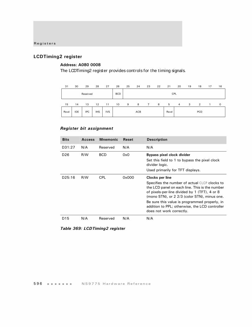
Reg i s t e r s
5 9 6 NS9775 Ha r dwa r e Re f e r ence
LCDTiming2 register
Address: A080 0008The LCDTiming2 register provides controls for the timing signals.
Register bit assignment
Bits Access Mnemonic Reset Description
D31:27 N/A Reserved N/A N/A
D26 R/W BCD 0x0 Bypass pixel clock dividerSet this field to 1 to bypass the pixel clock divider logic. Used primarily for TFT displays.
D25:16 R/W CPL 0x000 Clocks per lineSpecifies the number of actual CLCP clocks to the LCD panel on each line. This is the number of pixels-per-line divided by 1 (TFT), 4 or 8 (mono STN), or 2 2/3 (color STN), minus one. Be sure this value is programmed properly, in addition to PPL; otherwise, the LCD controller does not work correctly.
D15 N/A Reserved N/A N/A
Table 369: LCDTiming2 register
IPC IHS IVS ACB Rsvd PCD
13 12 11 10 9 8 7 6 5 4 3 2 1 015 14
Rsvd IOE
31 29 28 27 26 25 24 23 22 21 20 19 18 17 1630
BCD CPLReserved
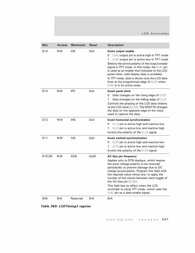
www.d i g i . com 597
LCD Con t r o l l e r
D14 R/W IOE 0x0 Invert output enable0 CLAC output pin is active high in TFT mode1 CLAC output pin is active low in TFT modeSelects the active polarity of the output enable signal in TFT mode. In this mode, the CLAC pin is used as an enable that indicates to the LCD panel when valid display data is available. In TFT mode, data is driven onto the LCD data lines at the programmed edge of CLCP when CLAC is in its active state.
D13 R/W IPC 0x0 Invert panel clock0 Data changes on the rising edge of CLCP.1 Data changes on the falling edge of CLCPControls the phasing of the LCD data relative to the LCD clock (CLCP). The NS9775 changes the data on the opposite edge of the clock used to capture the data.
D12 R/W IHS 0x0 Invert horizontal synchronization0 CLLP pin is active high and inactive low1 CLLP pin is active low and inactive highInverts the polarity of the CLLP signal.
D11 R/W IVS 0x0 Invert vertical synchronization0 CLFP pin is active high and inactive low1 CLFP pin is active low and inactive highInverts the polarity of the CLFP signal.
D10:06 R/W ACB 0x00 AC bias pin frequencyApplies only to STN displays, which require the pixel voltage polarity to be reversed periodically to prevent damage due to DC charge accumulation. Program this field with the required value minus one, to apply the number of line clocks between each toggle of the AC bias pin (CLAC). This field has no effect when the LCD controller is using TFT mode, which uses the CLAC pin as a data enable signal.
D05 N/A Reserved N/A N/A
Bits Access Mnemonic Reset Description
Table 369: LCDTiming2 register
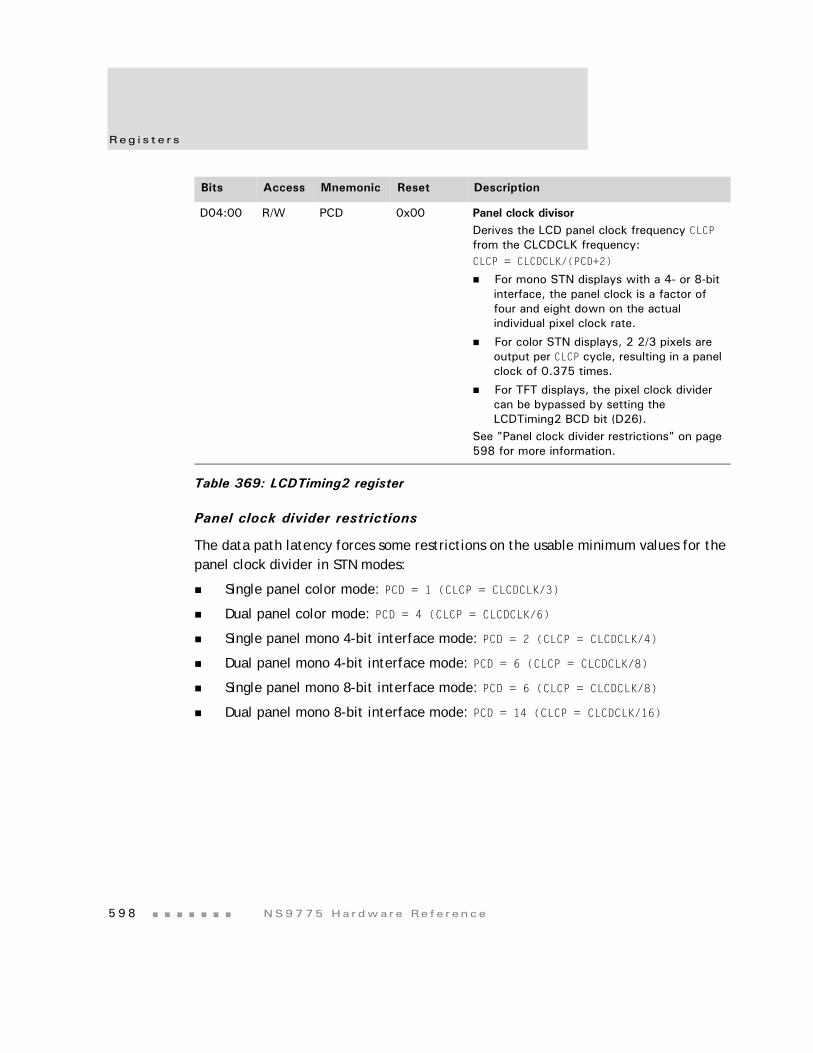
Reg i s t e r s
5 9 8 NS9775 Ha r dwa r e Re f e r ence
Panel clock divider restrictions
The data path latency forces some restrictions on the usable minimum values for the panel clock divider in STN modes:
Single panel color mode: PCD = 1 (CLCP = CLCDCLK/3)
Dual panel color mode: PCD = 4 (CLCP = CLCDCLK/6)
Single panel mono 4-bit interface mode: PCD = 2 (CLCP = CLCDCLK/4)
Dual panel mono 4-bit interface mode: PCD = 6 (CLCP = CLCDCLK/8)
Single panel mono 8-bit interface mode: PCD = 6 (CLCP = CLCDCLK/8)
Dual panel mono 8-bit interface mode: PCD = 14 (CLCP = CLCDCLK/16)
D04:00 R/W PCD 0x00 Panel clock divisorDerives the LCD panel clock frequency CLCP from the CLCDCLK frequency:CLCP = CLCDCLK/(PCD+2)
For mono STN displays with a 4- or 8-bit interface, the panel clock is a factor of four and eight down on the actual individual pixel clock rate.
For color STN displays, 2 2/3 pixels are output per CLCP cycle, resulting in a panel clock of 0.375 times.
For TFT displays, the pixel clock divider can be bypassed by setting the LCDTiming2 BCD bit (D26).
See "Panel clock divider restrictions" on page 598 for more information.
Bits Access Mnemonic Reset Description
Table 369: LCDTiming2 register
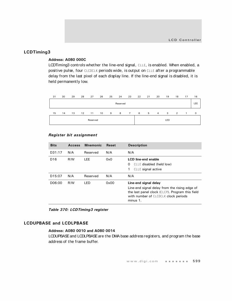
www.d i g i . com 599
LCD Con t r o l l e r
LCDTiming3
Address: A080 000CLCDTiming3 controls whether the line-end signal, CLLE, is enabled. When enabled, a positive pulse, four CLCDCLK periods wide, is output on CLLE after a programmable delay from the last pixel of each display line. If the line-end signal is disabled, it is held permanently low.
Register bit assignment
LCDUPBASE and LCDLPBASE
Address: A080 0010 and A080 0014LCDUPBASE and LCDLPBASE are the DMA base address registers, and program the base address of the frame buffer.
Bits Access Mnemonic Reset Description
D31:17 N/A Reserved N/A N/A
D16 R/W LEE 0x0 LCD line-end enable0 CLLE disabled (held low)1 CLLE signal active
D15:07 N/A Reserved N/A N/A
D06:00 R/W LED 0x00 Line-end signal delayLine-end signal delay from the rising edge of the last panel clock (CLCP). Program this field with number of CLCDCLK clock periods minus 1.
Table 370: LCDTiming3 register
LED
13 12 11 10 9 8 7 6 5 4 3 2 1 015 14
Reserved
31 29 28 27 26 25 24 23 22 21 20 19 18 17 1630
Reserved LEE
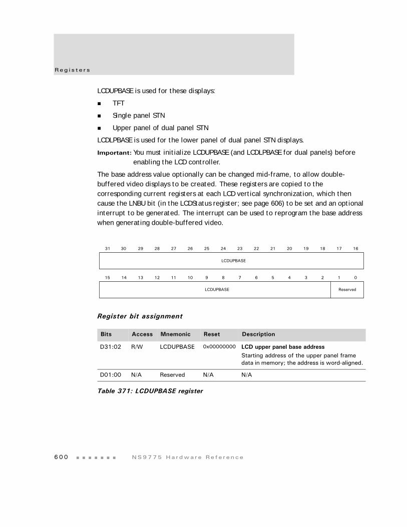
Reg i s t e r s
6 0 0 NS9775 Ha r dwa r e Re f e r ence
LCDUPBASE is used for these displays:
TFT
Single panel STN
Upper panel of dual panel STN
LCDLPBASE is used for the lower panel of dual panel STN displays.
Important: You must initialize LCDUPBASE (and LCDLPBASE for dual panels) before enabling the LCD controller.
The base address value optionally can be changed mid-frame, to allow double-buffered video displays to be created. These registers are copied to the corresponding current registers at each LCD vertical synchronization, which then cause the LNBU bit (in the LCDStatus register; see page 606) to be set and an optional interrupt to be generated. The interrupt can be used to reprogram the base address when generating double-buffered video.
Register bit assignment
Bits Access Mnemonic Reset Description
D31:02 R/W LCDUPBASE 0x00000000 LCD upper panel base addressStarting address of the upper panel frame data in memory; the address is word-aligned.
D01:00 N/A Reserved N/A N/A
Table 371: LCDUPBASE register
13 12 11 10 9 8 7 6 5 4 3 2 1 015 14
Reserved
31 29 28 27 26 25 24 23 22 21 20 19 18 17 1630
LCDUPBASE
LCDUPBASE
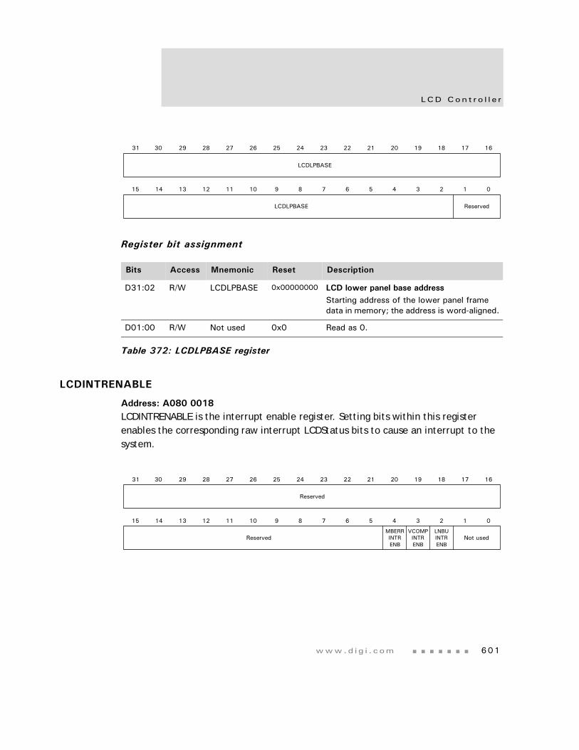
www.d i g i . com 601
LCD Con t r o l l e r
Register bit assignment
LCDINTRENABLE
Address: A080 0018LCDINTRENABLE is the interrupt enable register. Setting bits within this register enables the corresponding raw interrupt LCDStatus bits to cause an interrupt to the system.
Bits Access Mnemonic Reset Description
D31:02 R/W LCDLPBASE 0x00000000 LCD lower panel base addressStarting address of the lower panel frame data in memory; the address is word-aligned.
D01:00 R/W Not used 0x0 Read as 0.
Table 372: LCDLPBASE register
13 12 11 10 9 8 7 6 5 4 3 2 1 015 14
Reserved
31 29 28 27 26 25 24 23 22 21 20 19 18 17 1630
LCDLPBASE
LCDLPBASE
MBERRINTRENB
VCOMPINTRENB
13 12 11 10 9 8 7 6 5 4 3 2 1 015 14
31 29 28 27 26 25 24 23 22 21 20 19 18 17 1630
Reserved
Reserved Not usedLNBUINTRENB
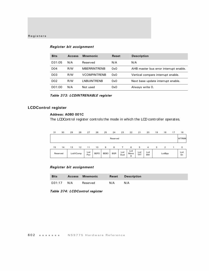
Reg i s t e r s
6 0 2 NS9775 Ha r dwa r e Re f e r ence
Register bit assignment
LCDControl register
Address: A080 001CThe LCDControl register controls the mode in which the LCD controller operates.
Register bit assignment
Bits Access Mnemonic Reset Description
D31:05 N/A Reserved N/A N/A
D04 R/W MBERRINTRENB 0x0 AHB master bus error interrupt enable.
D03 R/W VCOMPINTRENB 0x0 Vertical compare interrupt enable.
D02 R/W LNBUINTRENB 0x0 Next base update interrupt enable.
D01:00 N/A Not used 0x0 Always write 0.
Table 373: LCDINTRENABLE register
Bits Access Mnemonic Reset Description
D31:17 N/A Reserved N/A N/A
Table 374: LCDControl register
LcdPwr BEBO Lcd
Dual LcdBpp LcdEn
13 12 11 10 9 8 7 6 5 4 3 2 1 015 14
Reserved
31 29 28 27 26 25 24 23 22 21 20 19 18 17 1630
Reserved WTRMK
LcdVComp BEPO BGRLcd
Mono8
LcdTFT
LcdBW
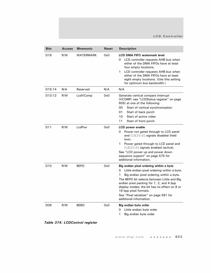
www.d i g i . com 603
LCD Con t r o l l e r
D16 R/W WATERMARK 0x0 LCD DMA FIFO watermark level0 LCD controller requests AHB bus when
either of the DMA FIFOs have at least four empty locations.
1 LCD controller requests AHB bus when either of the DMA FIFOs have at least eight empty locations. (Use this setting for optimum bus bandwidth.)
D15:14 N/A Reserved N/A N/A
D13:12 R/W LcdVComp 0x0 Generate vertical compare interrupt (VCOMP; see "LCDStatus register" on page 605) at one of the following:00 Start of vertical synchronization01 Start of back porch10 Start of active video11 Start of front porch
D11 R/W LcdPwr 0x0 LCD power enable0 Power not gated through to LCD panel
and CLD[23:0] signals disabled (held low).
1 Power gated through to LCD panel and CLD[23:0] signals enabled (active).
See "LCD power up and power down sequence support" on page 575 for additional information.
D10 R/W BEPO 0x0 Big endian pixel ordering within a byte0 Little endian pixel ordering within a byte.1 Big endian pixel ordering within a byte.The BEPO bit selects between Little and Big endian pixel packing for 1, 2, and 4 bpp display modes; the bit has no effect on 8 or 16 bpp pixel formats. See "Pixel serializer" on page 581 for additional information.
D09 R/W BEBO 0x0 Big endian byte order0 Little endian byte order1 Big endian byte order
Bits Access Mnemonic Reset Description
Table 374: LCDControl register
Reg i s t e r s
6 0 4 NS9775 Ha r dwa r e Re f e r ence
D08 R/W BGR 0x0 RGB or BGR format selection0 RGB: Normal output1 BGR: Red and blue swapped
D07 R/W LcdDual 0x0 LCD interface is dual panel STN0 Single panel LCD is in use.1 Dual panel LCD is in use.
D06 R/W LcdMono8 0x0 Monochrome LCD has 8-bit interface0 Mono LCD uses 4-bit interface.1 Mono LCD uses 8-bit interface.Controls whether monochrome STN LCD uses a 4- or 8-bit parallel interface. Program this bit to 0 for other modes.
D05 R/W LcdTFT 0x0 LCD is TFT0 LCD is STN display; use grayscaler.1 LCD is TFT; do not use grayscaler.
D04 R/W LcdBW 0x0 STN LCD is monochrome (black and white)0 STN LCD is color1 STN LCD is monochromeThis bit has no meaning in TFT mode.
D03:01 R/W LcdBpp 0x00 LCD bits per pixel000 1 bpp001 2 bpp010 4 bpp011 8 bpp100 16 bpp101 24 bpp (TFT panel only)110 Reserved111 Reserved
Bits Access Mnemonic Reset Description
Table 374: LCDControl register
www.d i g i . com 605
LCD Con t r o l l e r
LCDStatus register
Address: A080 0020The LCDStatus register provides raw interrupt status.
On a read, the register returns three bits that can generate interrupts when set.
On writes to the register, a bit value of 1 clears the interrupt corresponding to that bit. Writing a 0 has no effect.
Note: R/C indicates an access of read or clear.
Register bit assignment
D00 R/W LcdEn 0x0 LCD controller enable0 LCD signals CLLP, CLCP, CLFP, CLAC, and
CLLE disabled (held low).1 LCD signals CLLP, CLCP, CLFP, CLAC, and
CLLE enabled (active). See "LCD power up and power down sequence support" on page 575 for more information about LCD power sequencing.
Bits Access Mnemonic Reset Description
Table 374: LCDControl register
Bits Access Mnemonic Reset Description
D31:05 N/A Reserved N/A N/A
Table 375: LCDStatus register
MBERROR
VCOMP
13 12 11 10 9 8 7 6 5 4 3 2 1 015 14
31 29 28 27 26 25 24 23 22 21 20 19 18 17 1630
Reserved
Reserved ReservedLNBU
Reg i s t e r s
6 0 6 NS9775 Ha r dwa r e Re f e r ence
LCDInterrupt register
Address: A080 0024The LCDInterrupt register is a bit-by-bit logical AND of the LCDStatus register and the LCDINTRENABLE register. Interrupt lines correspond to each interrupt. A logical OR of all interrupts is provided to the system interrupt controller.
D04 R/C MBERROR 0x0 AHB master bus error statusSet when the AHB master encounters a bus error response from a slave.
D03 R/C VCOMP 0x0 Vertical compareSet when one of the four vertical regions, selected by the LCDControl register, is reached. (See LcdVcomp in "LCDControl register" on page 602).
D02 R/C LNBU 0x0 LCD next address base updateThis bit is mode-dependent, and is set when the current base address registers have been updated successfully by the next address registers. Signifies that a new next address can be loaded if double buffering is in use.
D01:00 N/A Reserved 0x0 N/A
Bits Access Mnemonic Reset Description
Table 375: LCDStatus register
MBERRORINTR
VCOMPINTR
13 12 11 10 9 8 7 6 5 4 3 2 1 015 14
31 29 28 27 26 25 24 23 22 21 20 19 18 17 1630
Reserved
Reserved ReservedLNBUINTR
www.d i g i . com 607
LCD Con t r o l l e r
Register bit assignment
LCDUPCURR and LCDLPCURR
Address: A080 0028 and A080 002CThe LCDUPCURR and LCDLPCURR registers contain an approximate value of the upper and lower panel data DMA addresses when read. The registers can change at any time, and therefore can be used only as a mechanism for coarse delay.
Register bit assignment
Bits Access Mnemonic Reset Description
D31:05 N/A Reserved N/A N/A
D04 R MBERRORINTR 0x0 AHB master bus error interrupt status bit.
D03 R VCOMPINTR 0x0 Vertical compare interrupt status bit.
D02 R LNBUINTR 0x0 LCD next base address update interrupt status bit.
D01:00 N/A Reserved N/A N/A
Table 376: LCDInterrupt register
Bits Access Mnemonic Reset Description
D31:00 R LCDUPCURR X LCD upper panel current address value.
Table 377: LCDUPCURR register
13 12 11 10 9 8 7 6 5 4 3 2 1 015 14
31 29 28 27 26 25 24 23 22 21 20 19 18 17 1630
LCDUPCURR
LCDUPCURR
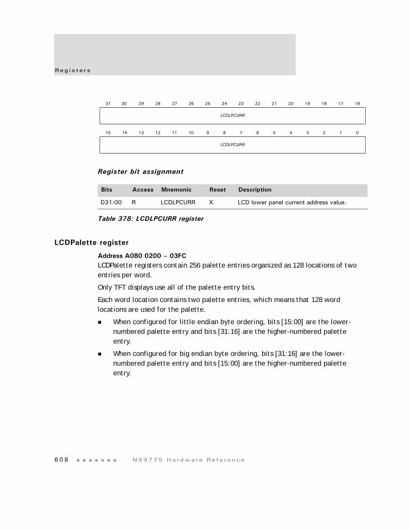
Reg i s t e r s
6 0 8 NS9775 Ha r dwa r e Re f e r ence
Register bit assignment
LCDPalette register
Address A080 0200 – 03FCLCDPalette registers contain 256 palette entries organized as 128 locations of two entries per word.
Only TFT displays use all of the palette entry bits.
Each word location contains two palette entries, which means that 128 word locations are used for the palette.
When configured for little endian byte ordering, bits [15:00] are the lower-numbered palette entry and bits [31:16] are the higher-numbered palette entry.
When configured for big endian byte ordering, bits [31:16] are the lower-numbered palette entry and bits [15:00] are the higher-numbered palette entry.
Bits Access Mnemonic Reset Description
D31:00 R LCDLPCURR X LCD lower panel current address value.
Table 378: LCDLPCURR register
13 12 11 10 9 8 7 6 5 4 3 2 1 015 14
31 29 28 27 26 25 24 23 22 21 20 19 18 17 1630
LCDLPCURR
LCDLPCURR
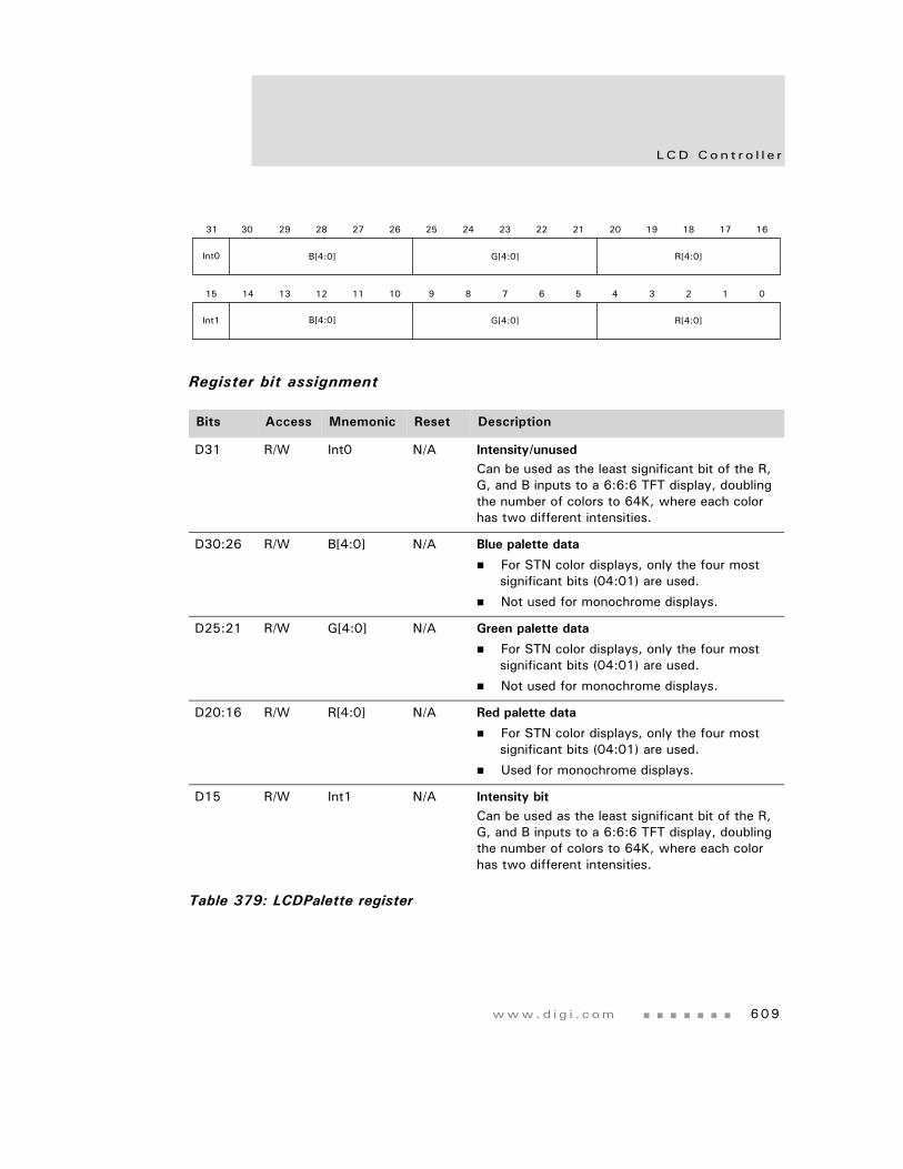
www.d i g i . com 609
LCD Con t r o l l e r
Register bit assignment
Bits Access Mnemonic Reset Description
D31 R/W Int0 N/A Intensity/unusedCan be used as the least significant bit of the R, G, and B inputs to a 6:6:6 TFT display, doubling the number of colors to 64K, where each color has two different intensities.
D30:26 R/W B[4:0] N/A Blue palette data
For STN color displays, only the four most significant bits (04:01) are used.
Not used for monochrome displays.
D25:21 R/W G[4:0] N/A Green palette data
For STN color displays, only the four most significant bits (04:01) are used.
Not used for monochrome displays.
D20:16 R/W R[4:0] N/A Red palette data
For STN color displays, only the four most significant bits (04:01) are used.
Used for monochrome displays.
D15 R/W Int1 N/A Intensity bitCan be used as the least significant bit of the R, G, and B inputs to a 6:6:6 TFT display, doubling the number of colors to 64K, where each color has two different intensities.
Table 379: LCDPalette register
13 12 11 10 9 8 7 6 5 4 3 2 1 015 14
Int1
31 29 28 27 26 25 24 23 22 21 20 19 18 17 1630
Int0 B[4:0] G[4:0] R[4:0]
B[4:0] G[4:0] R[4:0]
Reg i s t e r s
6 1 0 NS9775 Ha r dwa r e Re f e r ence
D14:10 R/W B[4:0] N/A Blue palette data
For STN color displays, only the four most significant bits (04:01) are used.
Not used for monochrome displays.
D09:05 R/W G[4:0] N/A Green palette data
For STN color displays, only the four most significant bits (04:01) are used.
Not used for monochrome displays.
D04:00 R/W R[4:0] N/A Red palette data
For STN color displays, only the four most significant bits (04:01) are used.
Used for monochrome displays.
Bits Access Mnemonic Reset Description
Table 379: LCDPalette register
www.d i g i . com 611
LCD Con t r o l l e r
Interrupts
The LCD controller drives a single interrupt back to the system, from four interrupt sources.
Each of the three individual maskable interrupt sources is enabled or disabled by changing the mask bits in the LCDINTRENABLE register. The status of the individual interrupt sources can be read from the LCDStatus register.
The interrupt sources are described next.
MBERRORINTR — Master bus error interrupt
The master bus error interrupt is asserted when an error response is received by the master interface during a transaction with a slave. When such an error occurs, the master interface enters an error state and remains in this state until the error is cleared (error clearance has been signalled to the master). When the respective interrupt service routine has completed, the master bus error interrupt can be cleared by writing a 1 to the MBERROR bit in the LCDStatus register. This action releases the master interface from its error state to the start of the frame state, allowing a fresh frame of data display to be initiated.
VCOMPINTR — Vertical compare interrupt
The vertical compare interrupt is asserted when one of the four vertical display regions, selected using the LCDControl register, is reached. The interrupt can occur at the beginning of one of the following:
Vertical synchronization
Back porch
Active video
Front porch
This interrupt can be cleared by writing a 1 to the Vcomp bit in the LCDStatus register.
I n t e r r u p t s
6 1 2 NS9775 Ha r dwa r e Re f e r ence
LBUINTR — Next base address update interrupt
The LCD next base address update interrupt is asserted when either the LCDUPBASE or LCDLPBASE values have been transferred to the LCDUPCURR or LCDLPCURR incrementers (respectively). This tells the system that it is safe to update the LCDUPBASE or LCDLPBASE registers with new frame base addresses, if required.
This interrupt can be cleared by writing a 1 to the LNBU bit in the LCDStatus register.
613
Serial Control Module: UART C H A P T E R 1 3
The NS9775 ASIC supports four independent universal asynchronous/synchronous receiver/transmitter channels. Each channel supports several modes, conditions, and formats.
Fea t u r e s
6 1 4 NS9775 Ha r dwa r e Re f e r ence
Features
Each channel supports these features:
DMA transfers to and from system memory
Independent programmable bit-rate generator
High speed data transfer: 1.8432 Mbps (asynchronous)
32-byte TX FIFO
32-Byte RX FIFO
Programmable data formats
– 5 to 8 data bits
– Odd, even, or no parity
– 1, 2 stop bits
Programmable channel modes
– Normal
– Loopback
– Remote loopback
– Control signal support: RTS, CTS, DTR, DSR, DCD, RI
Maskable interrupt conditions
– Receive FIFO ready
– Receive FIFO half full
– Transmit FIFO ready
– Transmit FIFO half empty
– CTS, DSR, DCD, RI state change detection
Multi-drop capable
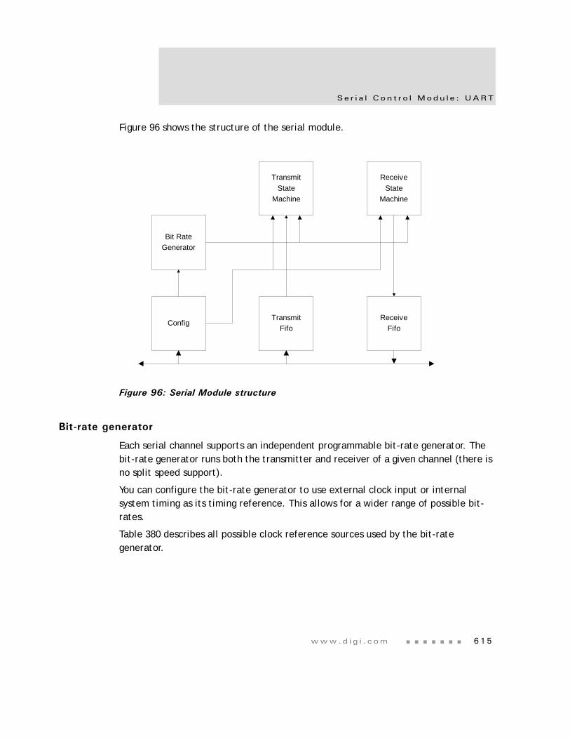
www.d i g i . com 615
Se r i a l Con t r o l Modu l e : UART
Figure 96 shows the structure of the serial module.
Figure 96: Serial Module structure
Bit-rate generator
Each serial channel supports an independent programmable bit-rate generator. The bit-rate generator runs both the transmitter and receiver of a given channel (there is no split speed support).
You can configure the bit-rate generator to use external clock input or internal system timing as its timing reference. This allows for a wider range of possible bit-rates.
Table 380 describes all possible clock reference sources used by the bit-rate generator.
Bit RateGenerator
ReceiveFifo
TransmitFifo
Config
ReceiveState
Machine
TransmitState
Machine
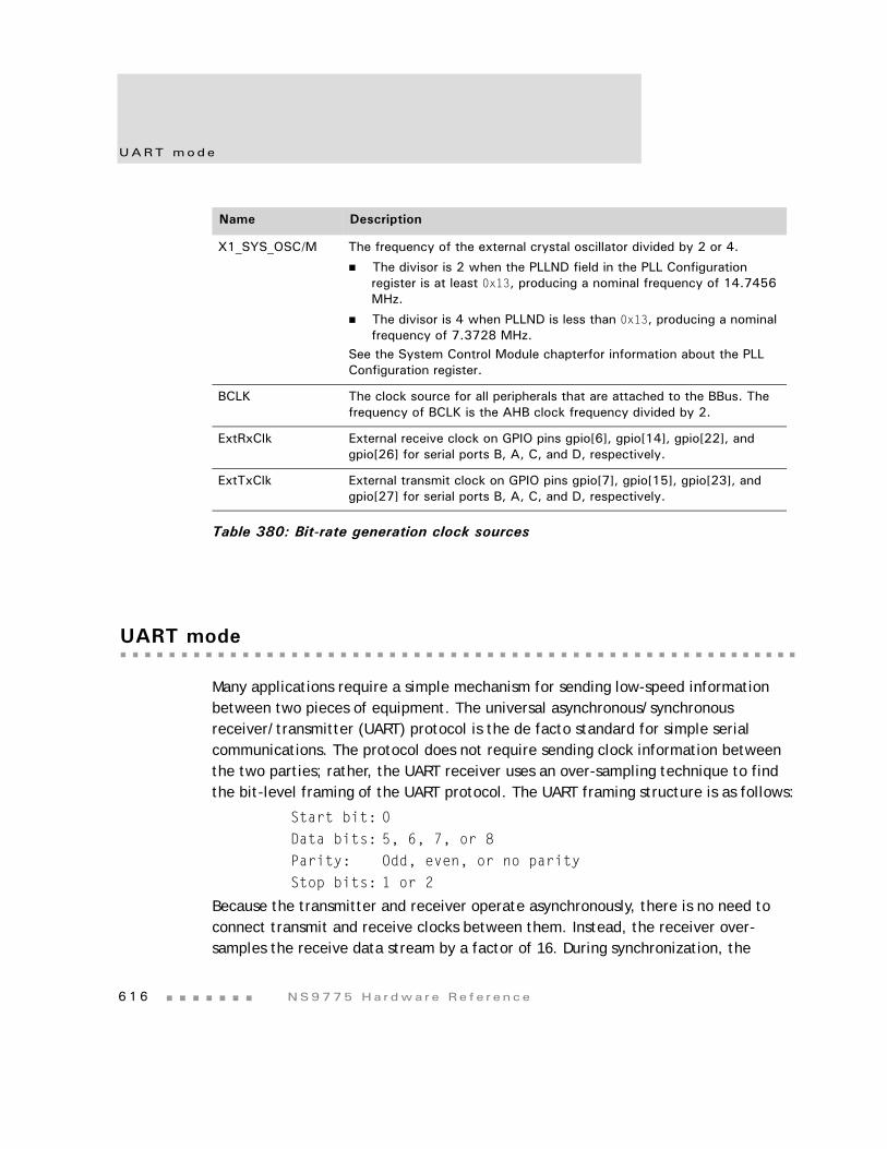
UART mode
6 1 6 NS9775 Ha r dwa r e Re f e r ence
UART mode
Many applications require a simple mechanism for sending low-speed information between two pieces of equipment. The universal asynchronous/synchronous receiver/transmitter (UART) protocol is the de facto standard for simple serial communications. The protocol does not require sending clock information between the two parties; rather, the UART receiver uses an over-sampling technique to find the bit-level framing of the UART protocol. The UART framing structure is as follows:
Start bit: 0
Data bits: 5, 6, 7, or 8
Parity: Odd, even, or no parity
Stop bits: 1 or 2
Because the transmitter and receiver operate asynchronously, there is no need to connect transmit and receive clocks between them. Instead, the receiver over-samples the receive data stream by a factor of 16. During synchronization, the
Name Description
X1_SYS_OSC/M The frequency of the external crystal oscillator divided by 2 or 4.
The divisor is 2 when the PLLND field in the PLL Configuration register is at least 0x13, producing a nominal frequency of 14.7456 MHz.
The divisor is 4 when PLLND is less than 0x13, producing a nominal frequency of 7.3728 MHz.
See the System Control Module chapterfor information about the PLL Configuration register.
BCLK The clock source for all peripherals that are attached to the BBus. The frequency of BCLK is the AHB clock frequency divided by 2.
ExtRxClk External receive clock on GPIO pins gpio[6], gpio[14], gpio[22], and gpio[26] for serial ports B, A, C, and D, respectively.
ExtTxClk External transmit clock on GPIO pins gpio[7], gpio[15], gpio[23], and gpio[27] for serial ports B, A, C, and D, respectively.
Table 380: Bit-rate generation clock sources
www.d i g i . com 617
Se r i a l Con t r o l Modu l e : UART
receiver waits for the start bit. When it finds the high-to-low transition, the receiver counts 8 sample times and uses this point as the bit-center for all remaining bits in the UART frame. Each bit-time is 16 clock ticks apart.
When the UART is not transmitting data, it transmits a continuous stream of ones — referred to as the IDLE condition. When data transmission begins, the transmitter sends the start bit and the receiver is enabled.
You can configure the UART to perform the following functions:
Enable the transmitter using the CTS handshaking signal. In this mode, the transmitter cannot start a new UART data frame unless CTS is active. If CTS is dropped anywhere in the middle of a UART data frame, the current character is completed and the next character is stalled.
Signal its receiver FIFO status using the RTS handshaking signal. When the receive FIFO has only four characters of available space, the RTS signal is dropped. The RTS and CTS pairs can be used for hardware flow control.
FIFO management
Data flow between a serial controller and memory occurs through the FIFO blocks within each serial controller module. Each serial controller provides both a 32-byte transmit FIFO and a 32-byte receive FIFO. Each FIFO is arranged as eight lines of four bytes to facilitate data transfer across BBus. Both the transmit and receive FIFOs are accessed using the Serial Channel B/A/C/D FIFO registers.
Transmit FIFO interface
The processor can write either 1, 2, 3, or 4 bytes at a time to the transmit FIFO. The number of bytes written is controlled by the data size defined by the HSIZE field on the AMBA AHB bus.
When the system is configured to operate in big endian mode, the most significant bytes in the word written to the FIFO are transmitted first. For example, the long word 0x11223344 results in the character 0x11 being transmitted first, and 0x44 being transmitted last.
F I FO managemen t
6 1 8 NS9775 Ha r dwa r e Re f e r ence
When the system is configured to operate in little endian mode, the least significant bytes in the word written to the FIFO are transmitted first. For example, the long word 0x11223344 results in the character 0x44 being transmitted first, and 0x11 being transmitted last.
Processor interrupts vs. DMA
The transmit FIFO can be filled using processor interrupts or the DMA controller.
Using processor interruptsThe processor can write one long word (4 bytes) of data to the transmit FIFO when the TRDY field in Serial Channel B/A/C/D Status Register A (see "Serial Channel B/A/C/D Status Register A," beginning on page 630) is active high. If the THALF field in Serial Channel B/A/C/D Status Register A is active high, the processor can write four long words (16 bytes) of data to the transmit FIFO. To facilitate an interrupt when either the TRDY or THALF status bits are active, the processor can set one or both of the corresponding interrupt enables (in "Serial Channel B/A/C/D Control Register A," beginning on page 623).
Using the DMA controllerWhen using the DMA controller, the processor need not interface with any of the serial port registers for data flow; rather, the processor must interface with the DMA channel registers and DMA buffer descriptor block. To facilitate the use of transmit DMA, the EXTDMA field in Serial Channel B/A/C/D Control Register A must be set active high. When the ETXDMA field is set active high, disable the serial transmitter interrupts.
Receive FIFO interface
The receive FIFO presents up to four bytes of data at a time to the processor interface. The number of valid bytes found in the next read of the FIFO is defined by the information in the RXFDB field (in "Serial Channel B/A/C/D Status Register A" on page 630).
When the system is configured to operate in big endian mode, the most significant bytes in the word written to the FIFO are read first. For example, the long word 0x11223344 results in the character 0x11 being read first, and 0x44 being read last.
www.d i g i . com 619
Se r i a l Con t r o l Modu l e : UART
When the system is configured to operate in little endian mode, the least significant bytes in the word written to the FIFO are read first. For example, the long word 0x11223344 results in the character 0x44 being read first, and 0x11 being read last.
When reading from the receive FIFO, the processor must perform a long word read operation. Each time a read cycle to the receive FIFO is performed, the receive FIFO advances to the next long word entry. The processor cannot read individual bytes from the same FIFO long word entry.
Processor interrupts vs. DMA
The receive FIFO can be emptied using processor interrupts or the DMA controller.
Using processor interruptsThe processor can read one long word (4 bytes) of data from the receive FIFO when the RRDY field (in "Serial Channel B/A/C/D Status Register A" on page 630) is set active high. The long word read may have 1, 2, 3, or 4 bytes of valid data within the word. The number of valid bytes is determined by the bit encoding in the RXFDB field in Serial Channel B/A/C/D Status Register A. The RXFDB field must be read before the FIFO Data register is read.
The RBC bit in Serial Channel B/A/C/D Status Register A indicates that a receive data buffer has been closed and receiver status can be read from this register. Before additional data can be read from the FIFO, the RBC bit must be acknowledged by writing a 1 to the same bit position in Serial Channel B/A/C/D Status Register A.
These steps provide the recommended process flow for the serial port receiver interrupt service routine:
1 Read Serial Channel B/A/C/D Status Register A.
2 If RRDY is true:
a Read the data FIFO.
b Use the RXFDB field to pick out valid bytes.
3 If RBC is true:
a Record receiver buffer closed status (if you want to).
b Write a 1 to the RBC bit position in Serial Channel B/A/C/D Status register A.
c Read Serial Channel B/A/C/D Status Register A again.
Se r i a l p o r t p e r f o rmance
6 2 0 NS9775 Ha r dwa r e Re f e r ence
To facilitate an interrupt when either the RRDY or RBC status bits are active, the processor must set one or both of the corresponding interrupt enables in Serial Channel B/A/C/D Control Register A.
Using the DMA controllerWhen using DMA, the processor need not interface with any of the serial port registers for data flow; rather, the processor must interface with the DMA channel registers and the DMA buffer descriptor block. To facilitate use of transmit DMA, the ERXDMA field in Serial Channel B/A/C/D Control register A must be set active high. When ERXDMA is set active high, disable the serial receiver interrupts.
Serial port performance
The serial ports have a finite performance limit on their ability to handle various serial protocols. The performance is limited by the speed of the SYSCLK operating the NS9775 ASIC. The configured speed for the internal PLL defines the BCLK rate; for UART (x8), the serial port maximum rate is 1834200 baud, for UART (x16), the serial port maximum rate is 921600 baud, and for UART (x32), the serial port maximum rate is 460800 baud.
Serial port control and status registers
All configuration registers must be accessed as 32-bit words and as single accesses only. No bursting is allowed.
The configuration registers for serial controller B are located at 0x9020_0000; the configuration registers for serial controller A are located at 0x9020_0040. Table 381 shows a single, two-channel address map for serial controllers B and A.
Address Description
9020 0000 Channel B Control Register A
9020 0004 Channel B Control Register B
Table 381: Serial channel B & A configuration registers
www.d i g i . com 621
Se r i a l Con t r o l Modu l e : UART
The configuration registers for serial controller C are located at 0x9030_0000; the configuration registers for serial controller D are located at 0x9030_0040. Table 382 shows a single, two-channel address map for serial controllers C and D.
9020 0008 Channel B Status Register A
9020 000C Channel B Bit-Rate register
9020 0010 Channel B FIFO Data register
9020 0014 Channel B Receive Buffer Gap Timer
9020 0018 Channel B Receive Character Gap Timer
9020 001C Channel B Receive Match register
9020 0020 Channel B Receive Match Mask register
9020 0034 Channel B Flow Control register
9020 0038 Channel B Flow Control Force register
9020 0040 Channel A Control Register A
9020 0044 Channel A Control Register B
9020 0048 Channel A Status Register A
9020 004C Channel A Bit-Rate register
9020 0050 Channel A FIFO Data register
9020 0054 Channel A Receive Buffer Gap Timer
9020 0058 Channel A Receive Character Gap Timer
9020 005C Channel A Receive Match register
9020 0060 Channel A Receive Match Mask register
9020 0074 Channel A Flow Control register
9020 0078 Channel A Flow Control Force register
Address Description
9030 0000 Channel C Control Register A
Table 382: Serial channel C & D configuration registers
Address Description
Table 381: Serial channel B & A configuration registers
Se r i a l p o r t con t r o l a nd s t a t u s r e g i s t e r s
6 2 2 NS9775 Ha r dwa r e Re f e r ence
9030 0004 Channel C Control Register B
9030 0008 Channel C Status Register A
9030 000C Channel C Bit-Rate register
9030 0010 Channel C FIFO Data register
9030 0014 Channel C Receive Buffer Gap Timer
9030 0018 Channel C Receive Character Gap Timer
9030 001C Channel C Receive Match register
9030 0020 Channel C Receive Match Mask register
9030 0034 Channel C Flow Control register
9030 0038 Channel C Flow Control Force register
9030 0040 Channel D Control Register A
9030 0044 Channel D Control Register B
9030 0048 Channel D Status Register A
9030 004C Channel D Bit-Rate register
9030 0050 Channel D FIFO Data register
9030 0054 Channel D Receive Buffer Gap Timer
9030 0058 Channel D Receive Character Gap Timer
9030 005C Channel D Receive Match register
9030 0060 Channel D Receive Match Mask register
9030 0074 Channel D Flow Control register
9030 0078 Channel D Flow Control Force register
Address Description
Table 382: Serial channel C & D configuration registers
www.d i g i . com 623
Se r i a l Con t r o l Modu l e : UART
Serial Channel B/A/C/D Control Register A
Address: 9020 0000 / 0040
9030 0000 / 0040There are two Serial Channel B/A/C/D Control Registers A within each two-channel serial controller module.
Register bit assignment
Bits Access Mnemonic Reset Description
D31 R/W CE 0 Channel enable0 Resets the port and the data FIFOs (disables
the channel)1 Enables a serial channel operationThe CE field must not be set until all control bits in Serial Channel Control Register A, Control Register B, and Bit-rate register have been defined.
D30 R/W BRK 0 Send breakForces a break condition in UART mode. While BRK is set to 1, the UART transmitter outputs a logic 0 or a space condition on the TXD output signal.
D29 R/W STICKP 0 Stick parityCan be used to force the UART parity field to a certain state as defined by the EPS field (see D28), instead of a parity bit calculated against the data word. STICKP applies only when the PE field (see D27) is also set to 1. Set STICKP to 1 to force transmission of the static parity value.
Table 383: Serial Channel B/A/C/D Control Register A
RIE ERXDMA RIC TIC ETX
DMA
13 12 11 10 9 8 7 6 5 4 3 2 1 015 14
31 29 28 27 26 25 24 23 22 21 20 19 18 17 1630
STICKP EPS STOPPE WLS CTSTX RTSRX RL LL Not used DTR RTSCE BRK
Not used
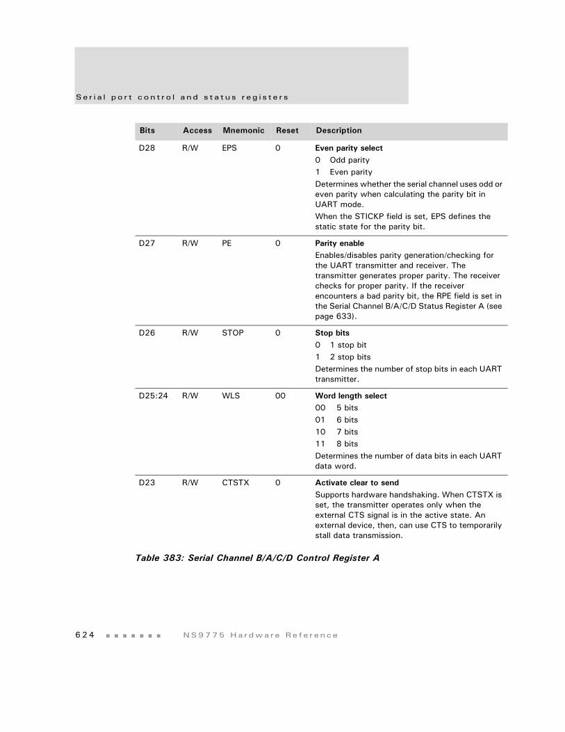
Se r i a l p o r t con t r o l a nd s t a t u s r e g i s t e r s
6 2 4 NS9775 Ha r dwa r e Re f e r ence
D28 R/W EPS 0 Even parity select0 Odd parity1 Even parityDetermines whether the serial channel uses odd or even parity when calculating the parity bit in UART mode.When the STICKP field is set, EPS defines the static state for the parity bit.
D27 R/W PE 0 Parity enableEnables/disables parity generation/checking for the UART transmitter and receiver. The transmitter generates proper parity. The receiver checks for proper parity. If the receiver encounters a bad parity bit, the RPE field is set in the Serial Channel B/A/C/D Status Register A (see page 633).
D26 R/W STOP 0 Stop bits0 1 stop bit1 2 stop bitsDetermines the number of stop bits in each UART transmitter.
D25:24 R/W WLS 00 Word length select00 5 bits01 6 bits10 7 bits11 8 bitsDetermines the number of data bits in each UART data word.
D23 R/W CTSTX 0 Activate clear to sendSupports hardware handshaking. When CTSTX is set, the transmitter operates only when the external CTS signal is in the active state. An external device, then, can use CTS to temporarily stall data transmission.
Bits Access Mnemonic Reset Description
Table 383: Serial Channel B/A/C/D Control Register A
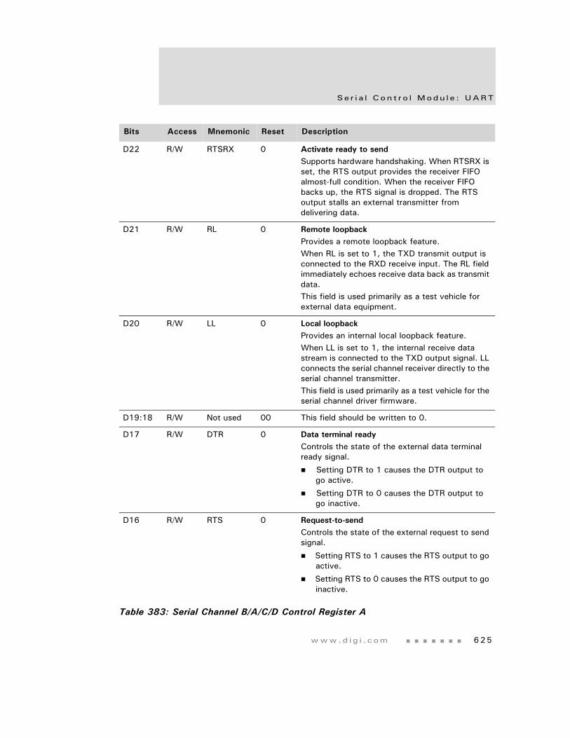
www.d i g i . com 625
Se r i a l Con t r o l Modu l e : UART
D22 R/W RTSRX 0 Activate ready to sendSupports hardware handshaking. When RTSRX is set, the RTS output provides the receiver FIFO almost-full condition. When the receiver FIFO backs up, the RTS signal is dropped. The RTS output stalls an external transmitter from delivering data.
D21 R/W RL 0 Remote loopbackProvides a remote loopback feature. When RL is set to 1, the TXD transmit output is connected to the RXD receive input. The RL field immediately echoes receive data back as transmit data. This field is used primarily as a test vehicle for external data equipment.
D20 R/W LL 0 Local loopbackProvides an internal local loopback feature. When LL is set to 1, the internal receive data stream is connected to the TXD output signal. LL connects the serial channel receiver directly to the serial channel transmitter. This field is used primarily as a test vehicle for the serial channel driver firmware.
D19:18 R/W Not used 00 This field should be written to 0.
D17 R/W DTR 0 Data terminal readyControls the state of the external data terminal ready signal.
Setting DTR to 1 causes the DTR output to go active.
Setting DTR to 0 causes the DTR output to go inactive.
D16 R/W RTS 0 Request-to-sendControls the state of the external request to send signal.
Setting RTS to 1 causes the RTS output to go active.
Setting RTS to 0 causes the RTS output to go inactive.
Bits Access Mnemonic Reset Description
Table 383: Serial Channel B/A/C/D Control Register A
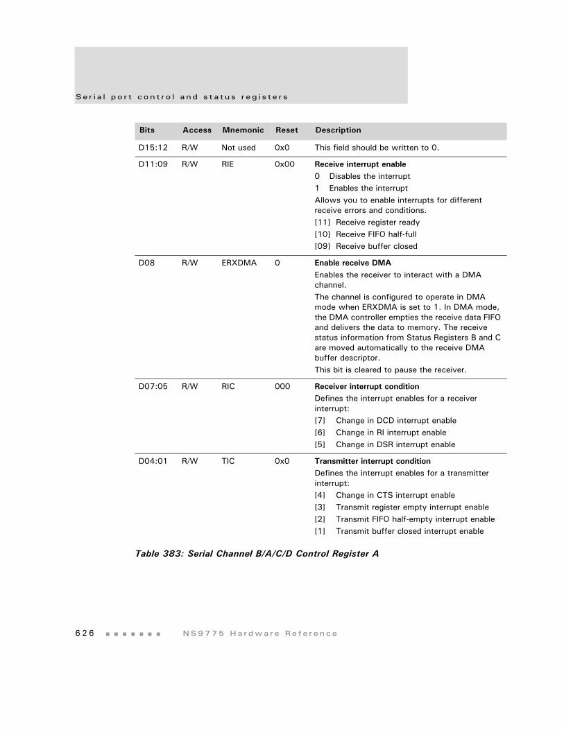
Se r i a l p o r t con t r o l a nd s t a t u s r e g i s t e r s
6 2 6 NS9775 Ha r dwa r e Re f e r ence
D15:12 R/W Not used 0x0 This field should be written to 0.
D11:09 R/W RIE 0x00 Receive interrupt enable0 Disables the interrupt1 Enables the interruptAllows you to enable interrupts for different receive errors and conditions.[11] Receive register ready[10] Receive FIFO half-full[09] Receive buffer closed
D08 R/W ERXDMA 0 Enable receive DMAEnables the receiver to interact with a DMA channel. The channel is configured to operate in DMA mode when ERXDMA is set to 1. In DMA mode, the DMA controller empties the receive data FIFO and delivers the data to memory. The receive status information from Status Registers B and C are moved automatically to the receive DMA buffer descriptor. This bit is cleared to pause the receiver.
D07:05 R/W RIC 000 Receiver interrupt conditionDefines the interrupt enables for a receiver interrupt:[7] Change in DCD interrupt enable[6] Change in RI interrupt enable[5] Change in DSR interrupt enable
D04:01 R/W TIC 0x0 Transmitter interrupt conditionDefines the interrupt enables for a transmitter interrupt:[4] Change in CTS interrupt enable[3] Transmit register empty interrupt enable[2] Transmit FIFO half-empty interrupt enable[1] Transmit buffer closed interrupt enable
Bits Access Mnemonic Reset Description
Table 383: Serial Channel B/A/C/D Control Register A
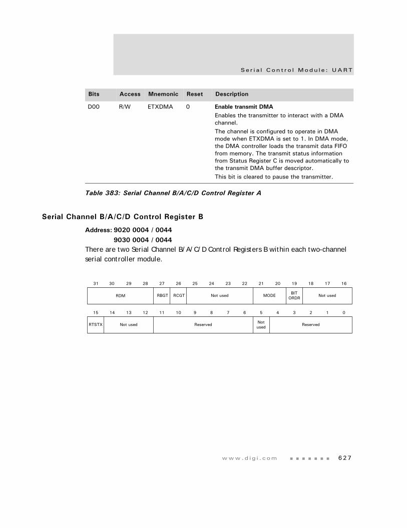
www.d i g i . com 627
Se r i a l Con t r o l Modu l e : UART
Serial Channel B/A/C/D Control Register B
Address: 9020 0004 / 0044
9030 0004 / 0044There are two Serial Channel B/A/C/D Control Registers B within each two-channel serial controller module.
D00 R/W ETXDMA 0 Enable transmit DMAEnables the transmitter to interact with a DMA channel.The channel is configured to operate in DMA mode when ETXDMA is set to 1. In DMA mode, the DMA controller loads the transmit data FIFO from memory. The transmit status information from Status Register C is moved automatically to the transmit DMA buffer descriptor. This bit is cleared to pause the transmitter.
Bits Access Mnemonic Reset Description
Table 383: Serial Channel B/A/C/D Control Register A
Reserved Reserved
13 12 11 10 9 8 7 6 5 4 3 2 1 015 14
31 29 28 27 26 25 24 23 22 21 20 19 18 17 1630
RCGTRBGT MODE Not usedBITORDRRDM
Not used
Not used
RTSTX Notused
Se r i a l p o r t con t r o l a nd s t a t u s r e g i s t e r s
6 2 8 NS9775 Ha r dwa r e Re f e r ence
Register bit assignment
Bits Access Mnemonic Reset Description
D31:28 R/W RDM 0x0 Enable receive data match[31] RDM1[30] RDM2[29] RDM3[28] RDM4Enables the receive data match comparators. A receive data match comparison detection can be used to close the current receive buffer descriptor. The last byte in the current receive data buffer contains the match character. Each of these bits enables the respective byte found in the Receive Match register.
D27 R/W RBGT 0 Receive buffer GAP timerDetects the maximum allowed time from when the first byte is placed into the receive data buffer and when the receive data buffer is closed.When RBGT is set to 1, the BGAP field in Serial Channel B/A/C/D Status Register A is set when the timeout value defined in the Receive Buffer GAP Timer register has expired.
D26 R/W RCGT 0 Receive character GAP timerDetects the maximum allowed time from when the last byte is placed into the receive data buffer and when the data buffer is closed.When RCGT is set to 1, the CGAP field in Serial Channel B/A/C/D Status Register A is set when the timeout value defined in the Receive Character GAP Timer register has expired.
D25:22 R/W Not used 0 Must be written as 0.
Table 384: Serial Channel B/A/C/D Control Register B
www.d i g i . com 629
Se r i a l Con t r o l Modu l e : UART
D21:20 R/W MODE 00 Serial channel mode00 UART mode01 Reserved10 SPI master mode11 SPI slave modeConfigures the serial channel to operate in UART or SPI mode. The MODE field must be set before the CE bit in Serial Channel B/A/C/D Control Register A is set to 1.
D19 R/W BITORDR 0 Bit ordering0 Bits are processed LSB first, MSB last1 Bits are processed MSB first, LSB lastControls the order in which bits are transmitted and received in the Serial Shift register.
D18:16 R/W Not used 0 Must be written as 0.
D15 R/W RTSTX 0 Enable active RTS only while transmittingControls the RTS indicator.When RTSTX is set, the RTS output goes active only when the transmitter is actively sending a transmit character. RTSTX allows external hardware to use the RTS signal as a transmit line driver enable signal in multi-drop applications.
Note: The RTS field in Serial Channel Control Register A must also be set. If the RTSRX field in Serial Channel Control Register A is set, however, do not set this — the RTSTX — field.
D14:12 R/W Not used 000 Must be written as 0.
D11:06 N/A Reserved N/A N/A
D05 R/W Not used 0 Must be written as 0.
D04:00 N/A Reserved N/A N/A
Bits Access Mnemonic Reset Description
Table 384: Serial Channel B/A/C/D Control Register B
Se r i a l p o r t con t r o l a nd s t a t u s r e g i s t e r s
6 3 0 NS9775 Ha r dwa r e Re f e r ence
Serial Channel B/A/C/D Status Register A
Address: 9020 0008 / 0048
9030 0008 / 0048The fields in Serial Channel B/A/C/D Status Register A operate differently when DMA mode is used. Many fields are not required for DMA mode, as they are copied to the status field in the DMA buffer descriptor. See the discussion of the DMA Buffer Descriptor register status field in the BBus DMA Controller chapter.
Bits Access Mnemonic Reset Description
D31:28 R MATCH 0x0 Match bit[31] Match1[30] Match2[29] Match3[28] Match4Set when a match character in the Receive Match register is configured at the same time that the enable receive data match bit is set in Serial Channel Control Register B (see "RDM" on page 628). The match bit indicates that a data match was found in the receive data stream, and the current receive data buffer has been closed. The last character in the receive data buffer contains the actual match character found. In DMA mode, the MATCH field is copied to bits [15:12] in the DMA buffer descriptor.
Table 385: Serial Channel B/A/C/D Status Register A
CTSI TEMPTY
13 12 11 10 9 8 7 6 5 4 3 2 1 015 14
31 29 28 27 26 25 24 23 22 21 20 19 18 17 1630
CGAPBGAP RXFDB DCDMatch
Not used
RBRK DSRI THALF
1 2 3 4RI DSR CTS
RFE RPE ROVER RRDY RHALF RBC RFS DCDI RII TRDY Notused
www.d i g i . com 631
Se r i a l Con t r o l Modu l e : UART
D27 R BGAP 0 Buffer GAP timerSet when the receive buffer GAP timer is set in Serial Channel Control Register B (see "RBGT" on page 628) and the timeout value defined in the Receive Buffer GAP Timer register has expired. This bit indicates that the maximum allowed time has passed since the first byte was placed into the receive data buffer. The receive data buffer is closed under this condition.In DMA mode, this field is copied to bit [11] in the DMA buffer descriptor.
D26 R CGAP 0 Character GAP timerSet when the enable receive character GAP timer is set in Serial Channel Control Register B (see "RCGT" on page 628) and the timeout value defined in the Receive Character GAP Timer register (see "Serial Channel B/A/C/D Receive Character GAP Timer" on page 646) has expired. This bit indicates that the maximum allowed time has passed since the previous byte was placed into the receive data buffer. The receive data buffer is closed under this condition.In DMA mode, this field is copied to bit [10] in the DMA buffer descriptor.
25:22 R Not used 0x0 This field is always read as 0x0.
D21:20 R RXFDB 00 Receive FIFO data available00 Full word01 One byte10 Half word11 Three bytesThis field is valid only when RRDY = 1.Identifies the number of valid bytes contained in the next long word to be read from the Serial Channel FIFO Data register. The next read of the FIFO can contain one, two, three, or four valid bytes of data. This field must be read before the FIFO is read to determine which bytes of the 4-byte long word contain valid data. Normal endian byte ordering rules apply to the Serial Channel FIFO Data register.
Bits Access Mnemonic Reset Description
Table 385: Serial Channel B/A/C/D Status Register A
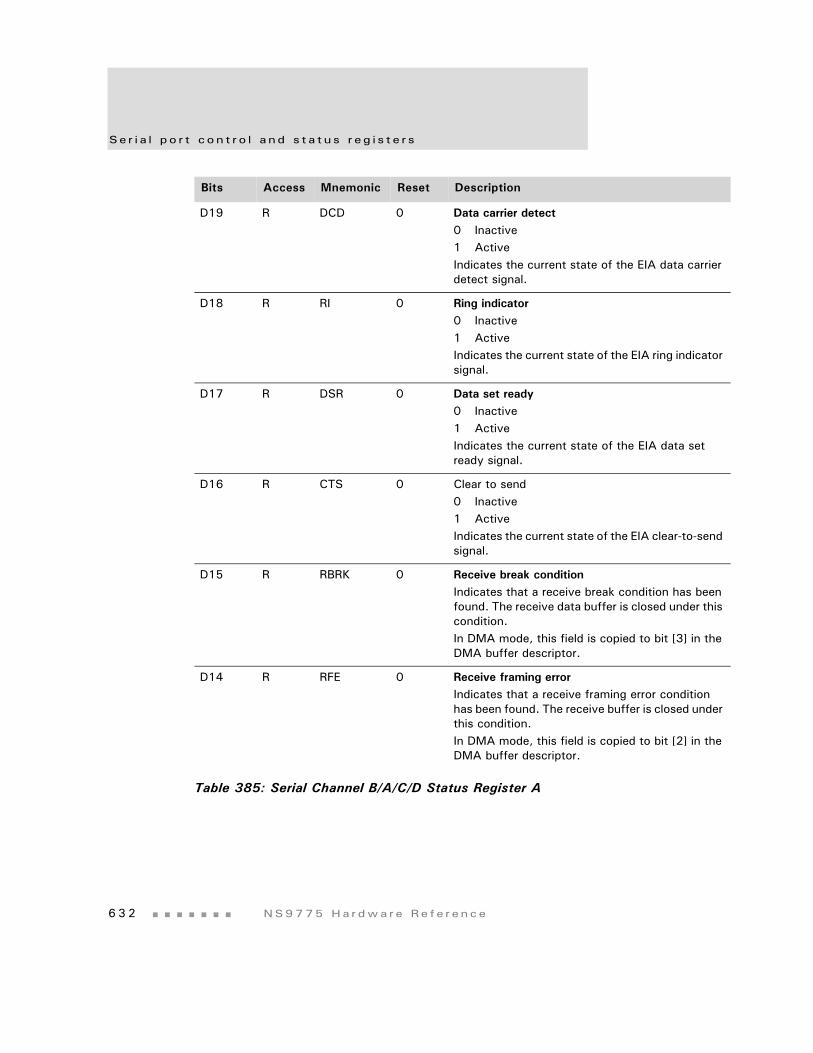
Se r i a l p o r t con t r o l a nd s t a t u s r e g i s t e r s
6 3 2 NS9775 Ha r dwa r e Re f e r ence
D19 R DCD 0 Data carrier detect0 Inactive1 ActiveIndicates the current state of the EIA data carrier detect signal.
D18 R RI 0 Ring indicator0 Inactive1 ActiveIndicates the current state of the EIA ring indicator signal.
D17 R DSR 0 Data set ready0 Inactive1 ActiveIndicates the current state of the EIA data set ready signal.
D16 R CTS 0 Clear to send0 Inactive1 ActiveIndicates the current state of the EIA clear-to-send signal.
D15 R RBRK 0 Receive break conditionIndicates that a receive break condition has been found. The receive data buffer is closed under this condition.In DMA mode, this field is copied to bit [3] in the DMA buffer descriptor.
D14 R RFE 0 Receive framing errorIndicates that a receive framing error condition has been found. The receive buffer is closed under this condition. In DMA mode, this field is copied to bit [2] in the DMA buffer descriptor.
Bits Access Mnemonic Reset Description
Table 385: Serial Channel B/A/C/D Status Register A
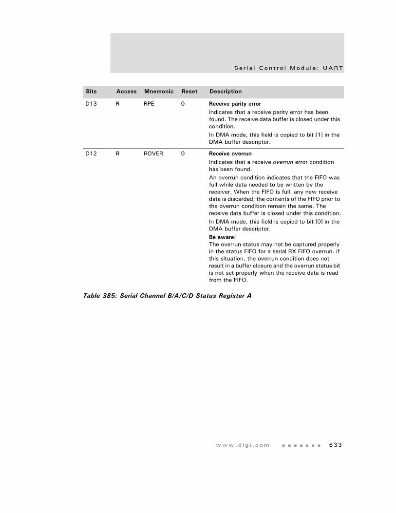
www.d i g i . com 633
Se r i a l Con t r o l Modu l e : UART
D13 R RPE 0 Receive parity errorIndicates that a receive parity error has been found. The receive data buffer is closed under this condition. In DMA mode, this field is copied to bit [1] in the DMA buffer descriptor.
D12 R ROVER 0 Receive overrunIndicates that a receive overrun error condition has been found. An overrun condition indicates that the FIFO was full while data needed to be written by the receiver. When the FIFO is full, any new receive data is discarded; the contents of the FIFO prior to the overrun condition remain the same. The receive data buffer is closed under this condition.In DMA mode, this field is copied to bit [0] in the DMA buffer descriptor.Be aware: The overrun status may not be captured properly in the status FIFO for a serial RX FIFO overrun. if this situation, the overrun condition does not result in a buffer closure and the overrun status bit is not set properly when the receive data is read from the FIFO.
Bits Access Mnemonic Reset Description
Table 385: Serial Channel B/A/C/D Status Register A
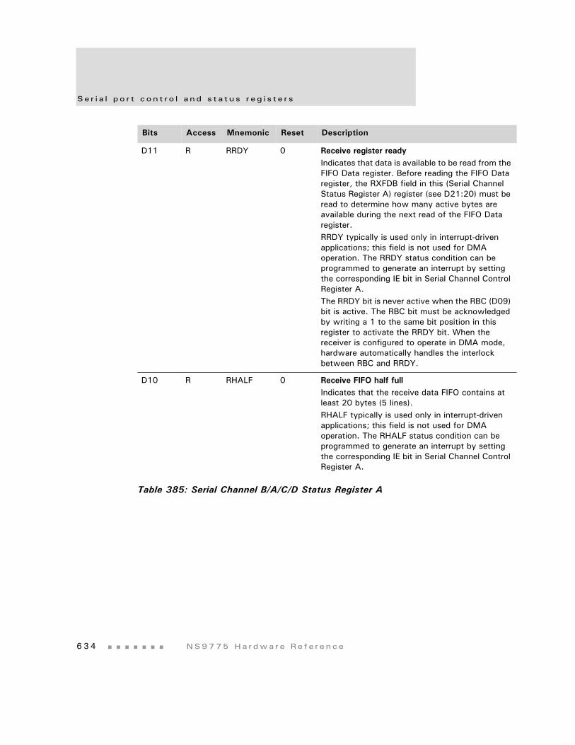
Se r i a l p o r t con t r o l a nd s t a t u s r e g i s t e r s
6 3 4 NS9775 Ha r dwa r e Re f e r ence
D11 R RRDY 0 Receive register readyIndicates that data is available to be read from the FIFO Data register. Before reading the FIFO Data register, the RXFDB field in this (Serial Channel Status Register A) register (see D21:20) must be read to determine how many active bytes are available during the next read of the FIFO Data register.RRDY typically is used only in interrupt-driven applications; this field is not used for DMA operation. The RRDY status condition can be programmed to generate an interrupt by setting the corresponding IE bit in Serial Channel Control Register A.The RRDY bit is never active when the RBC (D09) bit is active. The RBC bit must be acknowledged by writing a 1 to the same bit position in this register to activate the RRDY bit. When the receiver is configured to operate in DMA mode, hardware automatically handles the interlock between RBC and RRDY.
D10 R RHALF 0 Receive FIFO half fullIndicates that the receive data FIFO contains at least 20 bytes (5 lines). RHALF typically is used only in interrupt-driven applications; this field is not used for DMA operation. The RHALF status condition can be programmed to generate an interrupt by setting the corresponding IE bit in Serial Channel Control Register A.
Bits Access Mnemonic Reset Description
Table 385: Serial Channel B/A/C/D Status Register A
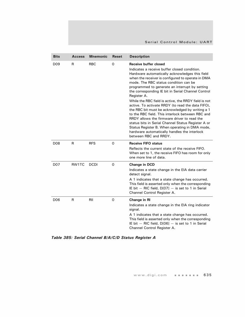
www.d i g i . com 635
Se r i a l Con t r o l Modu l e : UART
D09 R RBC 0 Receive buffer closedIndicates a receive buffer closed condition. Hardware automatically acknowledges this field when the receiver is configured to operate in DMA mode. The RBC status condition can be programmed to generate an interrupt by setting the corresponding IE bit in Serial Channel Control Register A. While the RBC field is active, the RRDY field is not active. To activate RRDY (to read the data FIFO), the RBC bit must be acknowledged by writing a 1 to the RBC field. This interlock between RBC and RRDY allows the firmware driver to read the status bits in Serial Channel Status Register A or Status Register B. When operating in DMA mode, hardware automatically handles the interlock between RBC and RRDY.
D08 R RFS 0 Receive FIFO statusReflects the current state of the receive FIFO. When set to 1, the receive FIFO has room for only one more line of data.
D07 RW1TC DCDI 0 Change in DCDIndicates a state change in the EIA data carrier detect signal.A 1 indicates that a state change has occurred. This field is asserted only when the corresponding IE bit — RIC field, D[07] — is set to 1 in Serial Channel Control Register A.
D06 R RII 0 Change in RIIndicates a state change in the EIA ring indicator signal. A 1 indicates that a state change has occurred. This field is asserted only when the corresponding IE bit — RIC field, D[06] — is set to 1 in Serial Channel Control Register A.
Bits Access Mnemonic Reset Description
Table 385: Serial Channel B/A/C/D Status Register A
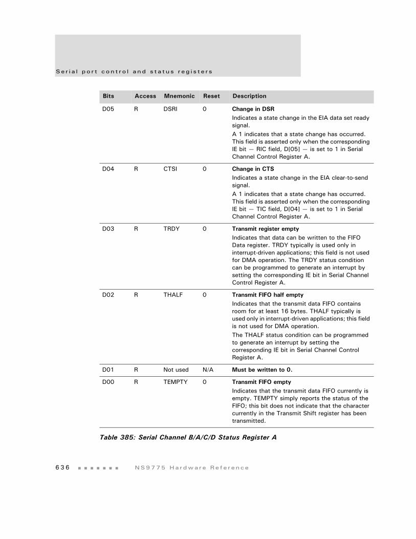
Se r i a l p o r t con t r o l a nd s t a t u s r e g i s t e r s
6 3 6 NS9775 Ha r dwa r e Re f e r ence
D05 R DSRI 0 Change in DSRIndicates a state change in the EIA data set ready signal.A 1 indicates that a state change has occurred. This field is asserted only when the corresponding IE bit — RIC field, D[05] — is set to 1 in Serial Channel Control Register A.
D04 R CTSI 0 Change in CTSIndicates a state change in the EIA clear-to-send signal.A 1 indicates that a state change has occurred. This field is asserted only when the corresponding IE bit — TIC field, D[04] — is set to 1 in Serial Channel Control Register A.
D03 R TRDY 0 Transmit register emptyIndicates that data can be written to the FIFO Data register. TRDY typically is used only in interrupt-driven applications; this field is not used for DMA operation. The TRDY status condition can be programmed to generate an interrupt by setting the corresponding IE bit in Serial Channel Control Register A.
D02 R THALF 0 Transmit FIFO half emptyIndicates that the transmit data FIFO contains room for at least 16 bytes. THALF typically is used only in interrupt-driven applications; this field is not used for DMA operation. The THALF status condition can be programmed to generate an interrupt by setting the corresponding IE bit in Serial Channel Control Register A.
D01 R Not used N/A Must be written to 0.
D00 R TEMPTY 0 Transmit FIFO emptyIndicates that the transmit data FIFO currently is empty. TEMPTY simply reports the status of the FIFO; this bit does not indicate that the character currently in the Transmit Shift register has been transmitted.
Bits Access Mnemonic Reset Description
Table 385: Serial Channel B/A/C/D Status Register A
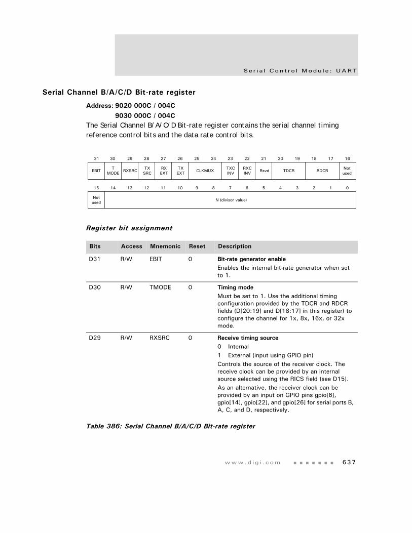
www.d i g i . com 637
Se r i a l Con t r o l Modu l e : UART
Serial Channel B/A/C/D Bit-rate register
Address: 9020 000C / 004C
9030 000C / 004CThe Serial Channel B/A/C/D Bit-rate register contains the serial channel timing reference control bits and the data rate control bits.
Register bit assignment
Bits Access Mnemonic Reset Description
D31 R/W EBIT 0 Bit-rate generator enableEnables the internal bit-rate generator when set to 1.
D30 R/W TMODE 0 Timing modeMust be set to 1. Use the additional timing configuration provided by the TDCR and RDCR fields (D[20:19] and D[18:17] in this register) to configure the channel for 1x, 8x, 16x, or 32x mode.
D29 R/W RXSRC 0 Receive timing source0 Internal1 External (input using GPIO pin)Controls the source of the receiver clock. The receive clock can be provided by an internal source selected using the RICS field (see D15).As an alternative, the receiver clock can be provided by an input on GPIO pins gpio[6], gpio[14], gpio[22], and gpio[26] for serial ports B, A, C, and D, respectively.
Table 386: Serial Channel B/A/C/D Bit-rate register
13 12 11 10 9 8 7 6 5 4 3 2 1 015 14
Notused N (divisor value)
31 29 28 27 26 25 24 23 22 21 20 19 18 17 1630
RXSRC TXSRC
TXEXT
RXEXT CLKMUX TXC
INVRXCINV Rsvd TDCR Not
usedEBIT TMODE RDCR
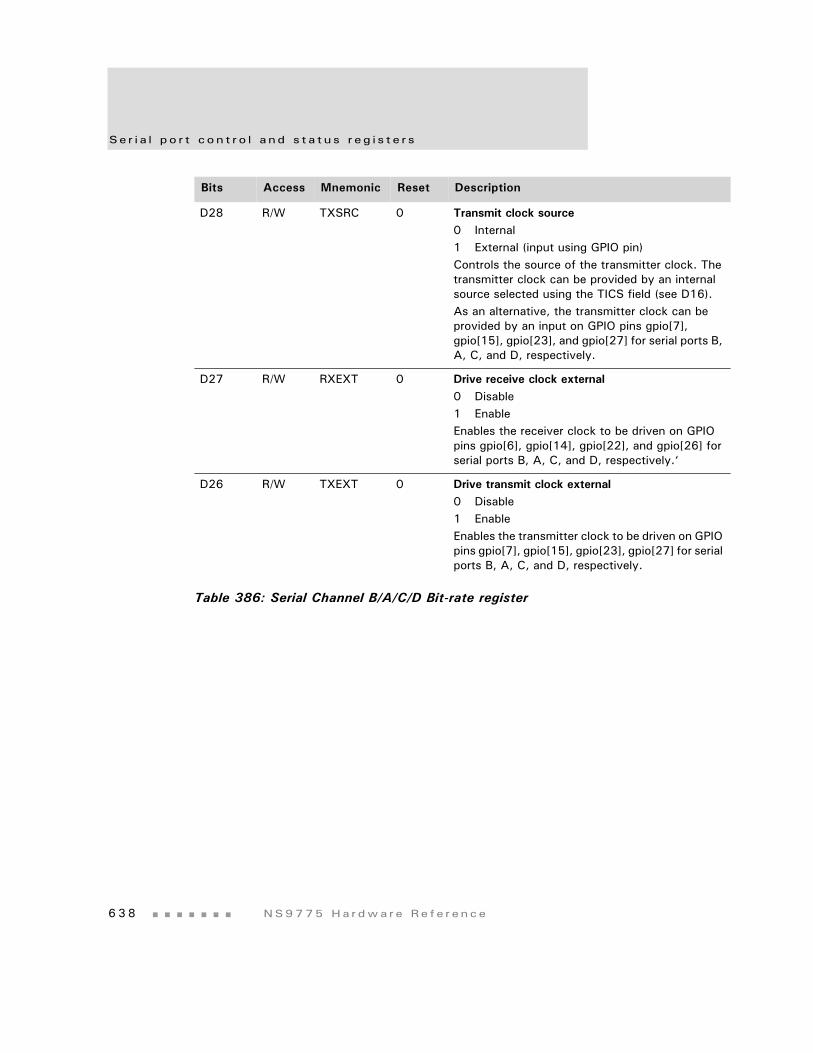
Se r i a l p o r t con t r o l a nd s t a t u s r e g i s t e r s
6 3 8 NS9775 Ha r dwa r e Re f e r ence
D28 R/W TXSRC 0 Transmit clock source0 Internal1 External (input using GPIO pin)Controls the source of the transmitter clock. The transmitter clock can be provided by an internal source selected using the TICS field (see D16).As an alternative, the transmitter clock can be provided by an input on GPIO pins gpio[7], gpio[15], gpio[23], and gpio[27] for serial ports B, A, C, and D, respectively.
D27 R/W RXEXT 0 Drive receive clock external0 Disable1 EnableEnables the receiver clock to be driven on GPIO pins gpio[6], gpio[14], gpio[22], and gpio[26] for serial ports B, A, C, and D, respectively.‘
D26 R/W TXEXT 0 Drive transmit clock external0 Disable1 EnableEnables the transmitter clock to be driven on GPIO pins gpio[7], gpio[15], gpio[23], gpio[27] for serial ports B, A, C, and D, respectively.
Bits Access Mnemonic Reset Description
Table 386: Serial Channel B/A/C/D Bit-rate register
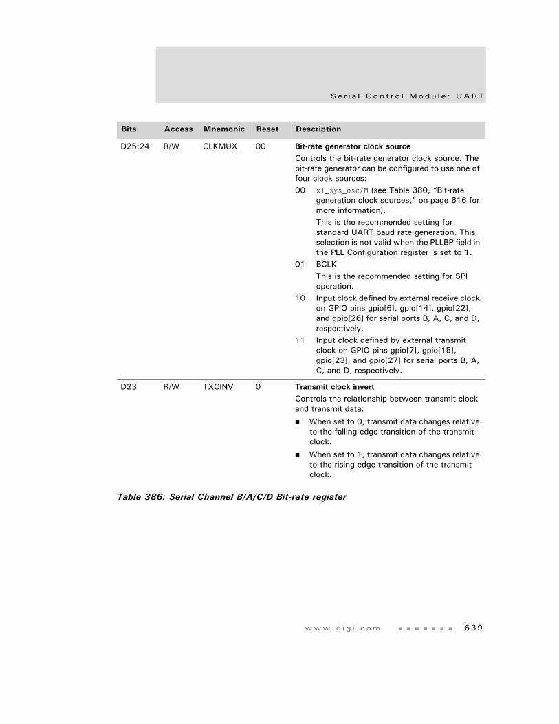
www.d i g i . com 639
Se r i a l Con t r o l Modu l e : UART
D25:24 R/W CLKMUX 00 Bit-rate generator clock sourceControls the bit-rate generator clock source. The bit-rate generator can be configured to use one of four clock sources:00 x1_sys_osc/M (see Table 380, “Bit-rate
generation clock sources,” on page 616 for more information). This is the recommended setting for standard UART baud rate generation. This selection is not valid when the PLLBP field in the PLL Configuration register is set to 1.
01 BCLKThis is the recommended setting for SPI operation.
10 Input clock defined by external receive clock on GPIO pins gpio[6], gpio[14], gpio[22], and gpio[26] for serial ports B, A, C, and D, respectively.
11 Input clock defined by external transmit clock on GPIO pins gpio[7], gpio[15], gpio[23], and gpio[27] for serial ports B, A, C, and D, respectively.
D23 R/W TXCINV 0 Transmit clock invertControls the relationship between transmit clock and transmit data:
When set to 0, transmit data changes relative to the falling edge transition of the transmit clock.
When set to 1, transmit data changes relative to the rising edge transition of the transmit clock.
Bits Access Mnemonic Reset Description
Table 386: Serial Channel B/A/C/D Bit-rate register
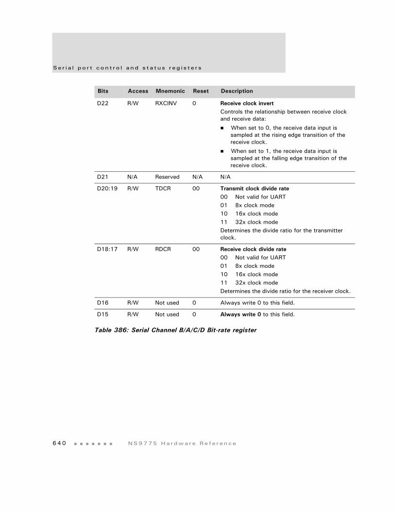
Se r i a l p o r t con t r o l a nd s t a t u s r e g i s t e r s
6 4 0 NS9775 Ha r dwa r e Re f e r ence
D22 R/W RXCINV 0 Receive clock invertControls the relationship between receive clock and receive data:
When set to 0, the receive data input is sampled at the rising edge transition of the receive clock.
When set to 1, the receive data input is sampled at the falling edge transition of the receive clock.
D21 N/A Reserved N/A N/A
D20:19 R/W TDCR 00 Transmit clock divide rate00 Not valid for UART01 8x clock mode10 16x clock mode11 32x clock modeDetermines the divide ratio for the transmitter clock.
D18:17 R/W RDCR 00 Receive clock divide rate00 Not valid for UART01 8x clock mode10 16x clock mode11 32x clock modeDetermines the divide ratio for the receiver clock.
D16 R/W Not used 0 Always write 0 to this field.
D15 R/W Not used 0 Always write 0 to this field.
Bits Access Mnemonic Reset Description
Table 386: Serial Channel B/A/C/D Bit-rate register
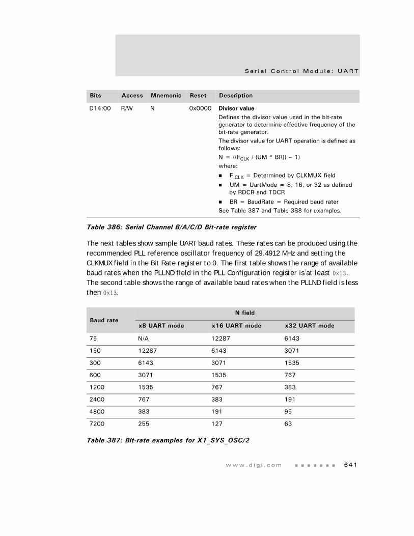
www.d i g i . com 641
Se r i a l Con t r o l Modu l e : UART
The next tables show sample UART baud rates. These rates can be produced using the recommended PLL reference oscillator frequency of 29.4912 MHz and setting the CLKMUX field in the Bit Rate register to 0. The first table shows the range of available baud rates when the PLLND field in the PLL Configuration register is at least 0x13. The second table shows the range of available baud rates when the PLLND field is less then 0x13.
D14:00 R/W N 0x0000 Divisor valueDefines the divisor value used in the bit-rate generator to determine effective frequency of the bit-rate generator. The divisor value for UART operation is defined as follows:N = ((FCLK / (UM * BR)) – 1)where:
F CLK = Determined by CLKMUX field
UM = UartMode = 8, 16, or 32 as defined by RDCR and TDCR
BR = BaudRate = Required baud raterSee Table 387 and Table 388 for examples.
Baud rateN field
x8 UART mode x16 UART mode x32 UART mode
75 N/A 12287 6143
150 12287 6143 3071
300 6143 3071 1535
600 3071 1535 767
1200 1535 767 383
2400 767 383 191
4800 383 191 95
7200 255 127 63
Table 387: Bit-rate examples for X1_SYS_OSC/2
Bits Access Mnemonic Reset Description
Table 386: Serial Channel B/A/C/D Bit-rate register
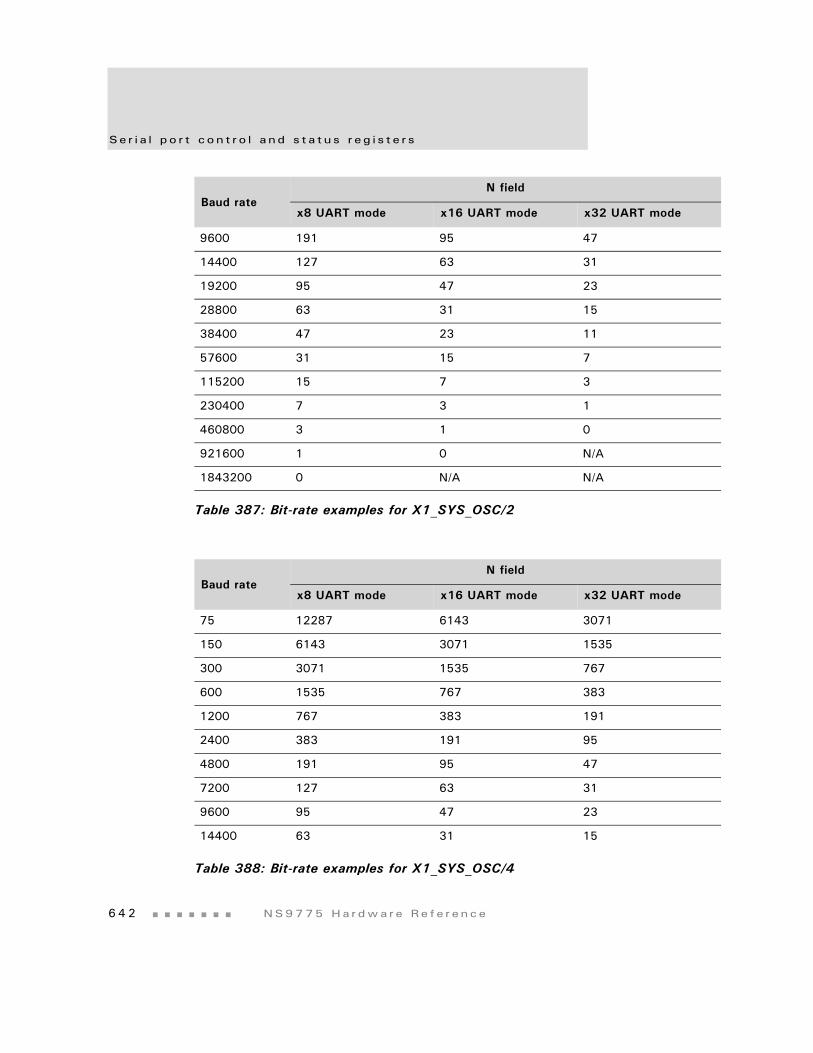
Se r i a l p o r t con t r o l a nd s t a t u s r e g i s t e r s
6 4 2 NS9775 Ha r dwa r e Re f e r ence
9600 191 95 47
14400 127 63 31
19200 95 47 23
28800 63 31 15
38400 47 23 11
57600 31 15 7
115200 15 7 3
230400 7 3 1
460800 3 1 0
921600 1 0 N/A
1843200 0 N/A N/A
Baud rateN field
x8 UART mode x16 UART mode x32 UART mode
75 12287 6143 3071
150 6143 3071 1535
300 3071 1535 767
600 1535 767 383
1200 767 383 191
2400 383 191 95
4800 191 95 47
7200 127 63 31
9600 95 47 23
14400 63 31 15
Table 388: Bit-rate examples for X1_SYS_OSC/4
Baud rateN field
x8 UART mode x16 UART mode x32 UART mode
Table 387: Bit-rate examples for X1_SYS_OSC/2
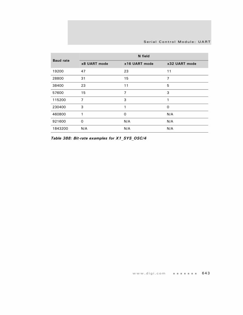
www.d i g i . com 643
Se r i a l Con t r o l Modu l e : UART
19200 47 23 11
28800 31 15 7
38400 23 11 5
57600 15 7 3
115200 7 3 1
230400 3 1 0
460800 1 0 N/A
921600 0 N/A N/A
1843200 N/A N/A N/A
Baud rateN field
x8 UART mode x16 UART mode x32 UART mode
Table 388: Bit-rate examples for X1_SYS_OSC/4
Se r i a l p o r t con t r o l a nd s t a t u s r e g i s t e r s
6 4 4 NS9775 Ha r dwa r e Re f e r ence
Serial Channel B/A/C/D FIFO Data register
Address: 9020 0010 / 0050
9030 0010 / 0050The Serial Channel B/A/C/D FIFO Data registers manually interface with the serial controller FIFOs instead of using DMA support.
Writing to the transmit register loads the transmit FIFO. This register can be written only when the TRDY field is set in Serial Channel Status Register A. Writing to the Serial Channel FIFO Data register automatically clears the TRDY bit.
Reading from the receive register empties the receive FIFO. Data is available when the RRDY bit is set in Serial Channel Status Register A. The RXFDB field in Serial Channel Status Register A identifies how many bytes are available to be read. Reading the Serial Channel FIFO Data register automatically clears the RRDY bit in Serial Channel Status Register A.
Register bit assignment
Bits Access Mnemonic Reset Description
D31:00 R/W DATA 0x00000000 Serial channel FIFO data field.
Table 389: Serial Channel B/A/C/D FIFO Data register
13 12 11 10 9 8 7 6 5 4 3 2 1 015 14
31 29 28 27 26 25 24 23 22 21 20 19 18 17 1630
DATA
DATA
www.d i g i . com 645
Se r i a l Con t r o l Modu l e : UART
Serial Channel B/A/C/D Receive Buffer GAP Timer
Address: 9020 0014 / 0054
9030 0014 / 0054The Receive Buffer GAP Timer closes out a receive serial data buffer. This timer can be configured to provide an interval in the range of 34.7uS to 2.27 S. The timer is reset when the first character is received in a new buffer. New characters are received while the timer operates; when the timer reaches its programmed threshold, the receive buffer is closed.
Register bit assignment
Bits Access Mnemonic Reset Description
D31 R/W TRUN 0 Buffer GAP timer enable0 Disables the timer1 Enables the timer
D30:16 R/W Not used 0x0000 Must be written as 0.
Table 390: Serial Channel B/A/C/D Receive Buffer GAP Timer
13 12 11 10 9 8 7 6 5 4 3 2 1 015 14
31 29 28 27 26 25 24 23 22 21 20 19 18 17 1630
Not used
Buffer GAP timer (BT)
TRUN
Se r i a l p o r t con t r o l a nd s t a t u s r e g i s t e r s
6 4 6 NS9775 Ha r dwa r e Re f e r ence
Serial Channel B/A/C/D Receive Character GAP Timer
Address: 9020 0018 / 0058
9030 0018 / 0058The receive character GAP timer closes out a receive serial data buffer due to a gap between characters. This timer is configured to provide an interval in the range of 0.27us to 0.28S. The timer is reset when a character is received. When the timer reaches its programmed threshold, the receive data buffer is closed.
D15:00 R/W BT 0x0000 Buffer GAP timerDefines the required value for the receive buffer GAP timer. BT is a function of the channel bit-rate and the receive buffer size. Recommended approach: Set the buffer GAP timer to be a value that is slightly larger than the amount of time required to fill the maximum buffer size using the channel bit-rate. Compute the BT value as shown:BT = (((Timeout * FCLK) / 512) - 1)where:
FCLK = (x1_sys_osc / M) (see Table 380 for examples)
Timeout = Appropriate timeout in seconds
Use the following equation to define the recommended buffer GAP timeout value. Timeout = (((BufferSize + 1) * 8) / DataRate)where:
BufferSize = receive buffer size in bytes
DataRate = interface data rate in bits
Bits Access Mnemonic Reset Description
Table 390: Serial Channel B/A/C/D Receive Buffer GAP Timer
www.d i g i . com 647
Se r i a l Con t r o l Modu l e : UART
Register bit assignment
Bits Access Mnemonic Reset Description
D31 R/W TRUN 0x0 Character GAP timer enable0 Disables the timer1 Enables the timer
D30:20 R/W Not used 0x000 Must be written as 0.
Table 391: Serial Channel B/A/C/D Receive Character GAP Timer
13 12 11 10 9 8 7 6 5 4 3 2 1 015 14
31 29 28 27 26 25 24 23 22 21 20 19 18 17 1630
Not used
Character GAP timer (CT)
TRUN Character GAP timer (CT)
Se r i a l p o r t con t r o l a nd s t a t u s r e g i s t e r s
6 4 8 NS9775 Ha r dwa r e Re f e r ence
Serial Channel B/A/C/D Receive Match register
Address: 9020 001C / 005C
9030 001C / 005CThe Serial Channel B/A/C/D Receive Match register contains the four receive data match bytes used in UART mode.
D19:00 CT CT 0x00000 Character GAP timerDefines the required value for the receive character GAP timer. Compute the CT value as shown:CT = (((Timeout * FCLK)/4) - 1where:
FCLK = (x1_sys_osc / M) (see Table 380 for examples)
Timeout = Appropriate timeout in seconds
Use the following equation to define the recommended character GAP timeout value:Timeout = (NumBitGap / DataRate)where:
NumBitGap = The number of bits in a character plus any start, stop, or parity bits.
DataRate = Interface data rate in bits per second.
Note: When PLL is bypassed, FCLK equals BCLK which equals x1_sys_osc/8. In most designs BCLK = (398.1312Mhz / 8) = 49.7664 Mhz.Examples:
Timeout=0.1ms ; CT field=0x004DB
Timeout=1.0ms ; CT field=0x03098
Timeout=5.0ms ; CT field=0x0F2FF
The maximum value that can be programmed into the CT field is 0x7FFFF.
Bits Access Mnemonic Reset Description
Table 391: Serial Channel B/A/C/D Receive Character GAP Timer
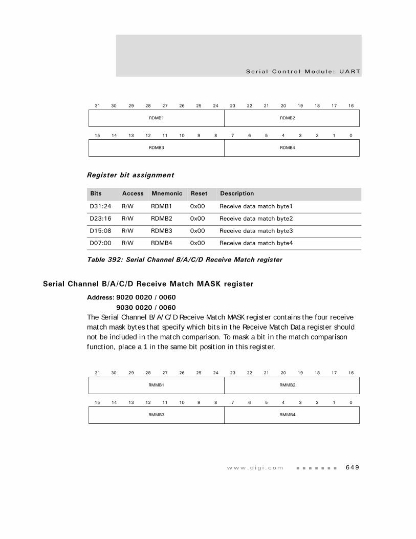
www.d i g i . com 649
Se r i a l Con t r o l Modu l e : UART
Register bit assignment
Serial Channel B/A/C/D Receive Match MASK register
Address: 9020 0020 / 0060
9030 0020 / 0060The Serial Channel B/A/C/D Receive Match MASK register contains the four receive match mask bytes that specify which bits in the Receive Match Data register should not be included in the match comparison. To mask a bit in the match comparison function, place a 1 in the same bit position in this register.
Bits Access Mnemonic Reset Description
D31:24 R/W RDMB1 0x00 Receive data match byte1
D23:16 R/W RDMB2 0x00 Receive data match byte2
D15:08 R/W RDMB3 0x00 Receive data match byte3
D07:00 R/W RDMB4 0x00 Receive data match byte4
Table 392: Serial Channel B/A/C/D Receive Match register
RDMB4
13 12 11 10 9 8 7 6 5 4 3 2 1 015 14
31 29 28 27 26 25 24 23 22 21 20 19 18 17 1630
RDMB1
RDMB3
RDMB2
RMMB4
13 12 11 10 9 8 7 6 5 4 3 2 1 015 14
31 29 28 27 26 25 24 23 22 21 20 19 18 17 1630
RMMB1
RMMB3
RMMB2
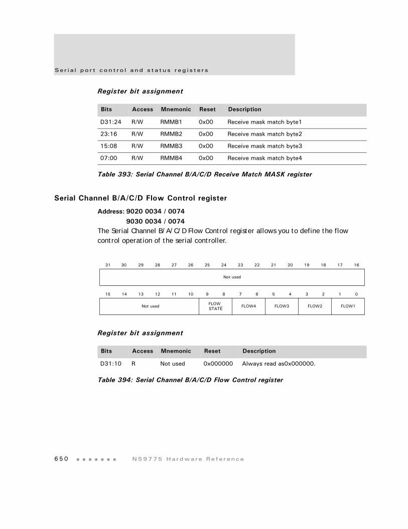
Se r i a l p o r t con t r o l a nd s t a t u s r e g i s t e r s
6 5 0 NS9775 Ha r dwa r e Re f e r ence
Register bit assignment
Serial Channel B/A/C/D Flow Control register
Address: 9020 0034 / 0074
9030 0034 / 0074The Serial Channel B/A/C/D Flow Control register allows you to define the flow control operation of the serial controller.
Register bit assignment
Bits Access Mnemonic Reset Description
D31:24 R/W RMMB1 0x00 Receive mask match byte1
23:16 R/W RMMB2 0x00 Receive mask match byte2
15:08 R/W RMMB3 0x00 Receive mask match byte3
07:00 R/W RMMB4 0x00 Receive mask match byte4
Table 393: Serial Channel B/A/C/D Receive Match MASK register
Bits Access Mnemonic Reset Description
D31:10 R Not used 0x000000 Always read as0x000000.
Table 394: Serial Channel B/A/C/D Flow Control register
FLOW_STATE
13 12 11 10 9 8 7 6 5 4 3 2 1 015 14
31 29 28 27 26 25 24 23 22 21 20 19 18 17 1630
Not used
Not used FLOW4 FLOW3 FLOW2 FLOW1
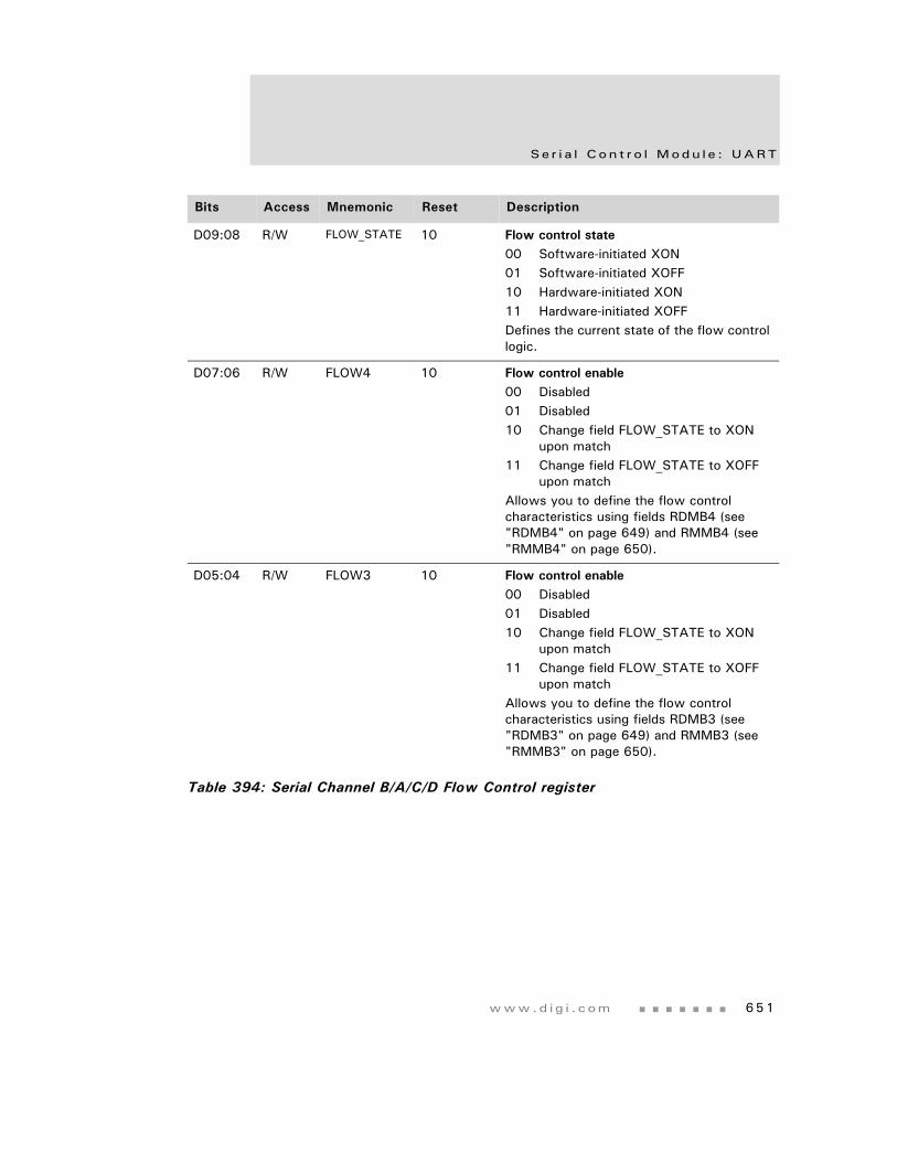
www.d i g i . com 651
Se r i a l Con t r o l Modu l e : UART
D09:08 R/W FLOW_STATE 10 Flow control state00 Software-initiated XON01 Software-initiated XOFF10 Hardware-initiated XON11 Hardware-initiated XOFFDefines the current state of the flow control logic.
D07:06 R/W FLOW4 10 Flow control enable00 Disabled01 Disabled10 Change field FLOW_STATE to XON
upon match11 Change field FLOW_STATE to XOFF
upon matchAllows you to define the flow control characteristics using fields RDMB4 (see "RDMB4" on page 649) and RMMB4 (see "RMMB4" on page 650).
D05:04 R/W FLOW3 10 Flow control enable00 Disabled01 Disabled10 Change field FLOW_STATE to XON
upon match11 Change field FLOW_STATE to XOFF
upon matchAllows you to define the flow control characteristics using fields RDMB3 (see "RDMB3" on page 649) and RMMB3 (see "RMMB3" on page 650).
Bits Access Mnemonic Reset Description
Table 394: Serial Channel B/A/C/D Flow Control register
Se r i a l p o r t con t r o l a nd s t a t u s r e g i s t e r s
6 5 2 NS9775 Ha r dwa r e Re f e r ence
Serial Channel B/A/C/D Flow Control Force register
Address: 9020 0038 / 0078
9030 0038 / 0078The Serial Channel B/A/C/D Flow Control Force register allows you to override the normal flow of transmit data.
D03:02 R/W FLOW2 10 Flow control enable00 Disabled01 Disabled10 Change field FLOW_STATE to XON
upon match11 Change field FLOW_STATE to XOFF
upon matchAllows you to define the flow control characteristics using fields RDMB2 (see "RDMB2" on page 649) and RMMB2 (see "RMMB2" on page 650).
D01:00 R/W FLOW1 10 Flow control enable00 Disabled01 Disabled10 Change field FLOW_STATE to XON
upon match11 Change field FLOW_STATE to XOFF
upon matchAllows you to define the flow control characteristics using fields RDMB1 (see "RDMB1" on page 649) and RMMB1 (see "RMMB1" on page 650).
Bits Access Mnemonic Reset Description
Table 394: Serial Channel B/A/C/D Flow Control register
13 12 11 10 9 8 7 6 5 4 3 2 1 015 14
31 29 28 27 26 25 24 23 22 21 20 19 18 17 1630
Not used
Not used
TX_IDLE
FORCE_CHAR
Not used TX_DIS
FORCE_EN
www.d i g i . com 653
Se r i a l Con t r o l Modu l e : UART
Register bit assignment
Bits Access Mnemonic Reset Description
D31:21 R Not used 0x000 Always read as 0x000.
D20 R TX_IDLE 0 Transmit idleIndicates whether the transmit state machine has been forced into an idle state by writing a 1 to the TX_DIS field (see D17).
D19:18 R Not used 00 Always read as 00.
D17 R/W TX_DIS 0 Transmit disableAllows you to force the transmit state machine into the idle state. If a transmission is in progress, the current byte will complete before the state machine moves into the idle state.Write a 1 to enable this feature.
D16 R/W FORCE_EN 0 Force transmitAllows you to force the transmitter to send the character specified by the FORCE_CHAR (see D07:00) field. All user-specified rules, such as bit order, parity, and number of stop bits, are enforced. Write this field only when TX_IDLE is set to 1. Hardware clears this field once the character has been transmitted.Write a 1 to enable this feature.
D15:08 R Not used 0x00 Always read as 0x00.
D07:00 R/W FORCE_CHAR
0x00 Force characterDefines the character that is to be forced out of the transmitter.
Table 395: Serial Channel B/A/C/D Flow Control Force register

655
Serial Control Module: SPI C H A P T E R 1 4
The NS9775 ASIC supports four independent universal asynchronous/synchronous receiver/transmitter channels. Each channel supports several modes, conditions, and formats.
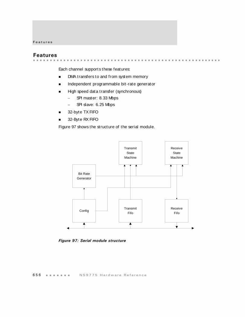
Fea t u r e s
6 5 6 NS9775 Ha r dwa r e Re f e r ence
Features
Each channel supports these features:
DMA transfers to and from system memory
Independent programmable bit-rate generator
High speed data transfer (synchronous)
– SPI master: 8.33 Mbps
– SPI slave: 6.25 Mbps
32-byte TX FIFO
32-Byte RX FIFO
Figure 97 shows the structure of the serial module.
Figure 97: Serial module structure
Bit RateGenerator
ReceiveFifo
TransmitFifo
Config
ReceiveState
Machine
TransmitState
Machine
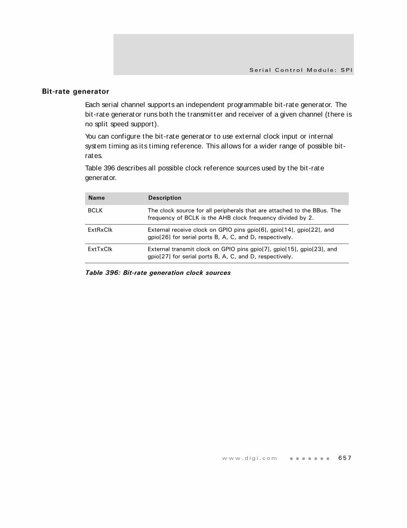
www.d i g i . com 657
Se r i a l Con t r o l Modu l e : SP I
Bit-rate generator
Each serial channel supports an independent programmable bit-rate generator. The bit-rate generator runs both the transmitter and receiver of a given channel (there is no split speed support).
You can configure the bit-rate generator to use external clock input or internal system timing as its timing reference. This allows for a wider range of possible bit-rates.
Table 396 describes all possible clock reference sources used by the bit-rate generator.
Name Description
BCLK The clock source for all peripherals that are attached to the BBus. The frequency of BCLK is the AHB clock frequency divided by 2.
ExtRxClk External receive clock on GPIO pins gpio[6], gpio[14], gpio[22], and gpio[26] for serial ports B, A, C, and D, respectively.
ExtTxClk External transmit clock on GPIO pins gpio[7], gpio[15], gpio[23], and gpio[27] for serial ports B, A, C, and D, respectively.
Table 396: Bit-rate generation clock sources
SP I mode
6 5 8 NS9775 Ha r dwa r e Re f e r ence
SPI mode
The NS9775 ASIC SPI controller provides these key features:
Four-wire interface (DATA_OUT, DATA_IN, CLK, ENABLE)
Master or slave configuration
Programmable MSB/LSB formatting
Programmable ENABLE polarity
Programmable SPI mode (0, 1, 2, 3)
The SPI controller provides a full-duplex, synchronous, character-oriented data channel between master and slave devices, using a four-wire interface (DATA_OUT, DATA_IN, CLK, ENABLE). The master interface operates in a broadcast mode. The slave interface is activated using the ENABLE signal. You can configure the master interface to address various slave interfaces using GPIO pins.
The transmitter and receiver use the same clock. When configured in master mode, the channel’s bit-rate generator (see "Bit-rate generator" on page 657) provides the timing reference.
SPI is useful for providing simple parallel/serial data conversion to stream serial data between memory and a peripheral. The SPI port has no protocol associated with it other than that it transfers information in multiples of 8 bits.
The SPI port simultaneously is capable of full duplex operation. The transfer of information is controlled by a single clock signal.
For the SPI master interface, the clock signal is an output.
For the SPI slave interface, the clock signal is an input.
The ENABLE signal also qualifies the transfer of information. The SPI ENABLE signal must be active for data transfers to occur, regardless of the SPI clock signal.
SPI modes
The four SPI modes are distinguished by the polarity in which the SPI CLK idles and the SPI CLK data phase used to capture SPI DATA_IN and drive SPI DATA_OUT. Table 397 describes the four modes and the register settings used to select the modes.
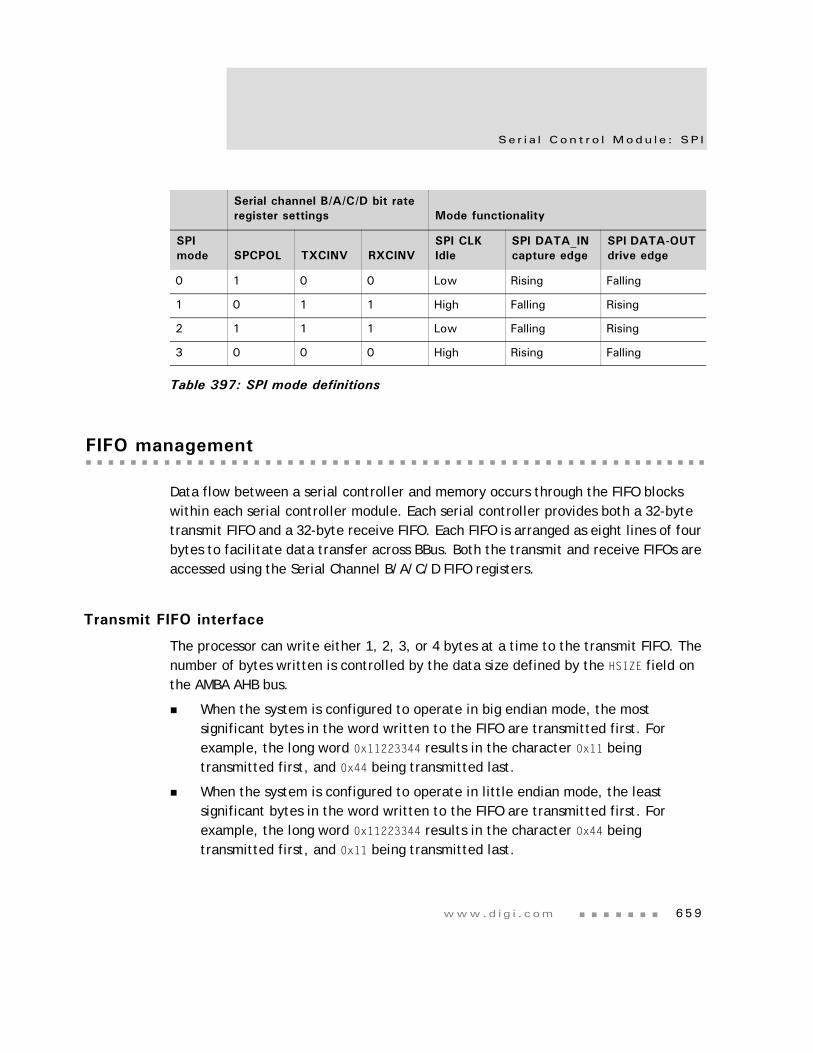
www.d i g i . com 659
Se r i a l Con t r o l Modu l e : SP I
FIFO management
Data flow between a serial controller and memory occurs through the FIFO blocks within each serial controller module. Each serial controller provides both a 32-byte transmit FIFO and a 32-byte receive FIFO. Each FIFO is arranged as eight lines of four bytes to facilitate data transfer across BBus. Both the transmit and receive FIFOs are accessed using the Serial Channel B/A/C/D FIFO registers.
Transmit FIFO interface
The processor can write either 1, 2, 3, or 4 bytes at a time to the transmit FIFO. The number of bytes written is controlled by the data size defined by the HSIZE field on the AMBA AHB bus.
When the system is configured to operate in big endian mode, the most significant bytes in the word written to the FIFO are transmitted first. For example, the long word 0x11223344 results in the character 0x11 being transmitted first, and 0x44 being transmitted last.
When the system is configured to operate in little endian mode, the least significant bytes in the word written to the FIFO are transmitted first. For example, the long word 0x11223344 results in the character 0x44 being transmitted first, and 0x11 being transmitted last.
Serial channel B/A/C/D bit rate register settings Mode functionality
SPI mode SPCPOL TXCINV RXCINV
SPI CLK Idle
SPI DATA_IN capture edge
SPI DATA-OUT drive edge
0 1 0 0 Low Rising Falling
1 0 1 1 High Falling Rising
2 1 1 1 Low Falling Rising
3 0 0 0 High Rising Falling
Table 397: SPI mode definitions
F I FO managemen t
6 6 0 NS9775 Ha r dwa r e Re f e r ence
Processor interrupts vs. DMA
The transmit FIFO can be filled using processor interrupts or the DMA controller.
Using processor interruptsThe processor can write one long word (4 bytes) of data to the transmit FIFO when the TRDY field in Serial Channel B/A/C/D Status Register A (see "Serial Channel B/A/C/D Status Register A," beginning on page 669) is active high. If the THALF field in Serial Channel B/A/C/D Status Register A is active high, the processor can write four long words (16 bytes) of data to the transmit FIFO. To facilitate an interrupt when either the TRDY or THALF status bits are active, the processor can set one or both of the corresponding interrupt enables (in "Serial Channel B/A/C/D Control Register A," beginning on page 664).
Using the DMA controllerWhen using the DMA controller, the processor need not interface with any of the serial port registers for data flow; rather, the processor must interface with the DMA channel registers and DMA buffer descriptor block. To facilitate the use of transmit DMA, the EXTDMA field in Serial Channel B/A/C/D Control Register A must be set active high. When the ETXDMA field is set active high, disable the serial transmitter interrupts.
Receive FIFO interface
The receive FIFO presents up to four bytes of data at a time to the processor interface. The number of valid bytes found in the next read of the FIFO is defined by the information in the RXFDB field (in "Serial Channel B/A/C/D Status Register A" on page 669).
When the system is configured to operate in big endian mode, the most significant bytes in the word written to the FIFO are read first. For example, the long word 0x11223344 results in the character 0x11 being read first, and 0x44 being read last.
When the system is configured to operate in little endian mode, the least significant bytes in the word written to the FIFO are read first. For example, the long word 0x11223344 results in the character 0x44 being read first, and 0x11 being read last.
www.d i g i . com 661
Se r i a l Con t r o l Modu l e : SP I
When reading from the receive FIFO, the processor must perform a long word read operation. Each time a read cycle to the receive FIFO is performed, the receive FIFO advances to the next long word entry. The processor cannot read individual bytes from the same FIFO long word entry.
Processor interrupts vs. DMA
The receive FIFO can be emptied using processor interrupts or the DMA controller.
Using processor interruptsThe processor can read one long word (4 bytes) of data from the receive FIFO when the RRDY field (in "Serial Channel B/A/C/D Status Register A" on page 669) is set active high. The long word read may have 1, 2, 3, or 4 bytes of valid data within the word. The number of valid bytes is determined by the bit encoding in the RXFDB field in Serial Channel B/A/C/D Status Register A. The RXFDB field must be read before the FIFO Data register is read.
The RBC bit in Serial Channel B/A/C/D Status Register A indicates that a receive data buffer has been closed and receiver status can be read from this register. Before additional data can be read from the FIFO, the RBC bit must be acknowledged by writing a 1 to the same bit position in Serial Channel B/A/C/D Status Register A.
These steps provide the recommended process flow for the serial port receiver interrupt service routine:
1 Read Serial Channel B/A/C/D Status Register A.
2 If RRDY is true:
a Read the data FIFO.
b Use the RXFDB field to pick out valid bytes.
3 If RBC is true:
a Record receiver buffer closed status (if you want to).
b Write a 1 to the RBC bit position in Serial Channel B/A/C/D Status register A.
c Read Serial Channel B/A/C/D Status Register A again.
To facilitate an interrupt when either the RRDY or RBC status bits are active, the processor must set one or both of the corresponding interrupt enables in Serial Channel B/A/C/D Control Register A.
Se r i a l p o r t p e r f o rmance
6 6 2 NS9775 Ha r dwa r e Re f e r ence
Using the DMA controllerWhen using DMA, the processor need not interface with any of the serial port registers for data flow; rather, the processor must interface with the DMA channel registers and the DMA buffer descriptor block. To facilitate use of transmit DMA, the ERXDMA field in Serial Channel B/A/C/D Control register A must be set active high. When ERXDMA is set active high, disable the serial receiver interrupts.
Serial port performance
The serial ports have a finite performance limit on their ability to handle various serial protocols. The performance is limited by the speed of the SYSCLK operating the NS9775 ASIC. The configured speed for the internal PLL defines the BCLK rate; for SPI, the serial port maximum rate is BCLK/8.
Serial port control and status registers
All configuration registers must be accessed as 32-bit words and as single accesses only. No bursting is allowed.
The configuration registers for serial controller B are located at 0x9020_0000; the configuration registers for serial controller A are located at 0x9020_0040. Table 398 shows a single, two-channel address map for serial controllers B and A.
Address Description
9020 0000 Channel B Control Register A
9020 0004 Channel B Control Register B
9020 0008 Channel B Status Register A
9020 000C Channel B Bit-Rate register
9020 0010 Channel B FIFO Data register
9020 0014 Channel B Receive Buffer Gap Timer
Table 398: Serial channel B & A configuration registers
www.d i g i . com 663
Se r i a l Con t r o l Modu l e : SP I
The configuration registers for serial controller C are located at 0x9030_0000; the configuration registers for serial controller D are located at 0x9030_0040. Table 399 shows a single, two-channel address map for serial controllers C and D.
9020 0018 Channel B Receive Character Gap Timer
9020 001C Channel B Receive Match register
9020 0020 Channel B Receive Match Mask register
9020 0038 Channel B Flow Control Force register
9020 0040 Channel A Control Register A
9020 0044 Channel A Control Register B
9020 0048 Channel A Status Register A
9020 004C Channel A Bit-Rate register
9020 0050 Channel A FIFO Data register
9020 0054 Channel A Receive Buffer Gap Timer
9020 0058 Channel A Receive Character Gap Timer
9020 005C Channel A Receive Match register
9020 0060 Channel A Receive Match Mask register
9020 0078 Channel A Flow Control Force register
Address Description
9030 0000 Channel C Control Register A
9030 0004 Channel C Control Register B
9030 0008 Channel C Status Register A
9030 000C Channel C Bit-Rate register
9030 0010 Channel C FIFO Data register
9030 0014 Channel C Receive Buffer Gap Timer
9030 0018 Channel C Receive Character Gap Timer
Table 399: Serial channel C & D configuration registers
Address Description
Table 398: Serial channel B & A configuration registers
Se r i a l p o r t con t r o l a nd s t a t u s r e g i s t e r s
6 6 4 NS9775 Ha r dwa r e Re f e r ence
Serial Channel B/A/C/D Control Register A
Address: 9020 0000 / 0040
9030 0000 / 0040There are two Serial Channel B/A/C/D Control Registers A within each two-channel serial controller module.
9030 001C Channel C Receive Match register
9030 0020 Channel C Receive Match Mask register
9030 0038 Channel C Flow Control Force register
9030 0040 Channel D Control Register A
9030 0044 Channel D Control Register B
9030 0048 Channel D Status Register A
9030 004C Channel D Bit-Rate register
9030 0050 Channel D FIFO Data register
9030 0054 Channel D Receive Buffer Gap Timer
9030 0058 Channel D Receive Character Gap Timer
9030 005C Channel D Receive Match register
9030 0060 Channel D Receive Match Mask register
9030 0078 Channel D Flow Control Force register
Address Description
Table 399: Serial channel C & D configuration registers
RIE ERXDMA Reserved TIC ETX
DMA
13 12 11 10 9 8 7 6 5 4 3 2 1 015 14
31 29 28 27 26 25 24 23 22 21 20 19 18 17 1630
RL LL Not usedCE
Not used
Not usedNot used WLS
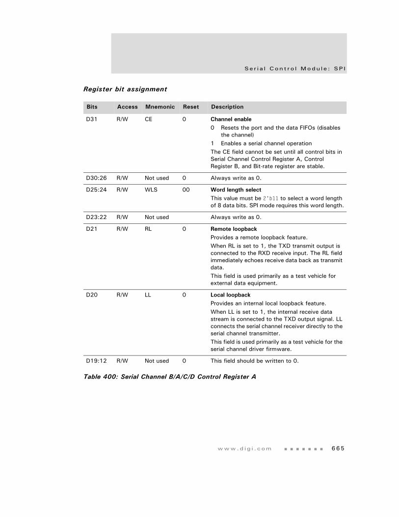
www.d i g i . com 665
Se r i a l Con t r o l Modu l e : SP I
Register bit assignment
Bits Access Mnemonic Reset Description
D31 R/W CE 0 Channel enable0 Resets the port and the data FIFOs (disables
the channel)1 Enables a serial channel operationThe CE field cannot be set until all control bits in Serial Channel Control Register A, Control Register B, and Bit-rate register are stable.
D30:26 R/W Not used 0 Always write as 0.
D25:24 R/W WLS 00 Word length selectThis value must be 2’b11 to select a word length of 8 data bits. SPI mode requires this word length.
D23:22 R/W Not used Always write as 0.
D21 R/W RL 0 Remote loopbackProvides a remote loopback feature. When RL is set to 1, the TXD transmit output is connected to the RXD receive input. The RL field immediately echoes receive data back as transmit data. This field is used primarily as a test vehicle for external data equipment.
D20 R/W LL 0 Local loopbackProvides an internal local loopback feature. When LL is set to 1, the internal receive data stream is connected to the TXD output signal. LL connects the serial channel receiver directly to the serial channel transmitter. This field is used primarily as a test vehicle for the serial channel driver firmware.
D19:12 R/W Not used 0 This field should be written to 0.
Table 400: Serial Channel B/A/C/D Control Register A
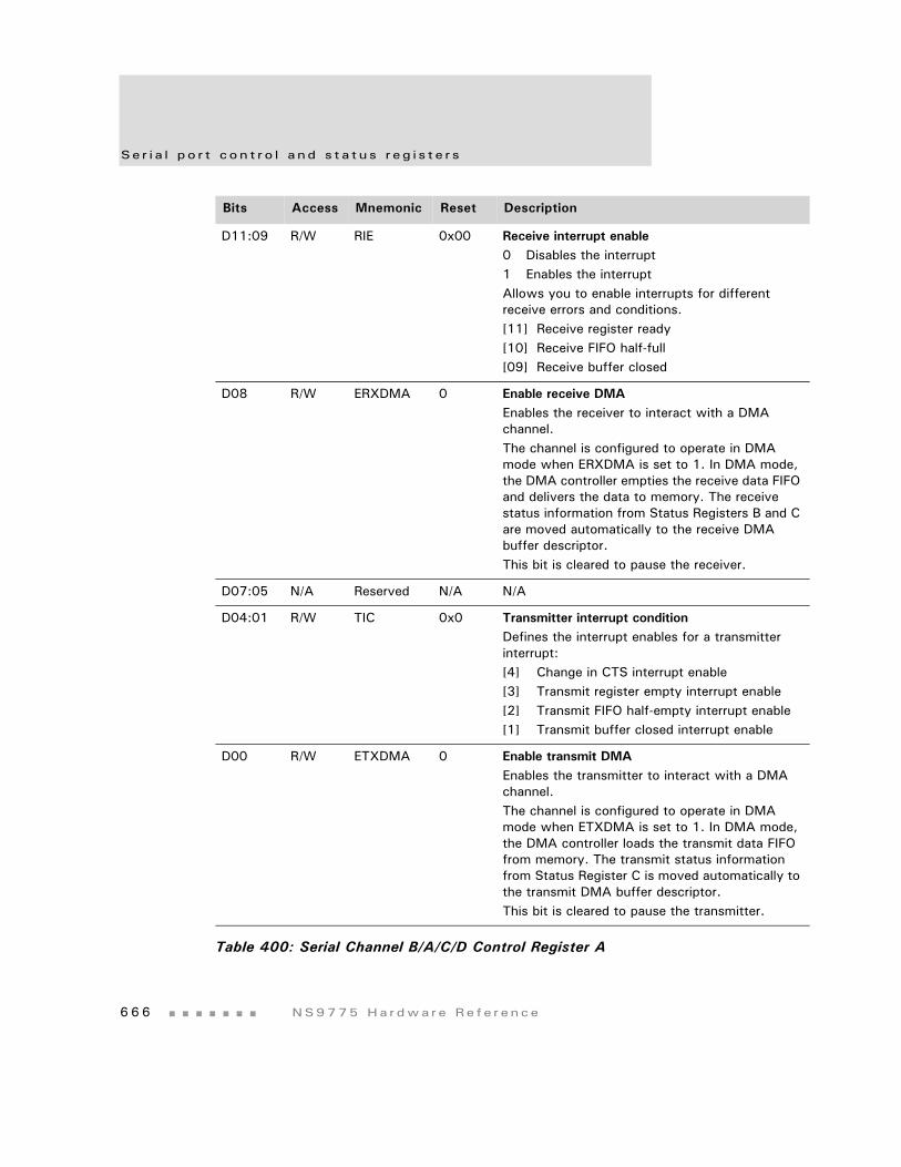
Se r i a l p o r t con t r o l a nd s t a t u s r e g i s t e r s
6 6 6 NS9775 Ha r dwa r e Re f e r ence
D11:09 R/W RIE 0x00 Receive interrupt enable0 Disables the interrupt1 Enables the interruptAllows you to enable interrupts for different receive errors and conditions.[11] Receive register ready[10] Receive FIFO half-full[09] Receive buffer closed
D08 R/W ERXDMA 0 Enable receive DMAEnables the receiver to interact with a DMA channel. The channel is configured to operate in DMA mode when ERXDMA is set to 1. In DMA mode, the DMA controller empties the receive data FIFO and delivers the data to memory. The receive status information from Status Registers B and C are moved automatically to the receive DMA buffer descriptor. This bit is cleared to pause the receiver.
D07:05 N/A Reserved N/A N/A
D04:01 R/W TIC 0x0 Transmitter interrupt conditionDefines the interrupt enables for a transmitter interrupt:[4] Change in CTS interrupt enable[3] Transmit register empty interrupt enable[2] Transmit FIFO half-empty interrupt enable[1] Transmit buffer closed interrupt enable
D00 R/W ETXDMA 0 Enable transmit DMAEnables the transmitter to interact with a DMA channel.The channel is configured to operate in DMA mode when ETXDMA is set to 1. In DMA mode, the DMA controller loads the transmit data FIFO from memory. The transmit status information from Status Register C is moved automatically to the transmit DMA buffer descriptor. This bit is cleared to pause the transmitter.
Bits Access Mnemonic Reset Description
Table 400: Serial Channel B/A/C/D Control Register A
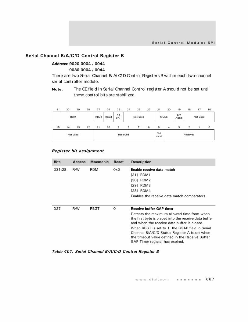
www.d i g i . com 667
Se r i a l Con t r o l Modu l e : SP I
Serial Channel B/A/C/D Control Register B
Address: 9020 0004 / 0044
9030 0004 / 0044There are two Serial Channel B/A/C/D Control Registers B within each two-channel serial controller module.
Note: The CE field in Serial Channel Control register A should not be set until these control bits are stabilized.
Register bit assignment
Bits Access Mnemonic Reset Description
D31:28 R/W RDM 0x0 Enable receive data match[31] RDM1[30] RDM2[29] RDM3[28] RDM4Enables the receive data match comparators.
D27 R/W RBGT 0 Receive buffer GAP timerDetects the maximum allowed time from when the first byte is placed into the receive data buffer and when the receive data buffer is closed.When RBGT is set to 1, the BGAP field in Serial Channel B/A/C/D Status Register A is set when the timeout value defined in the Receive Buffer GAP Timer register has expired.
Table 401: Serial Channel B/A/C/D Control Register B
Reserved
13 12 11 10 9 8 7 6 5 4 3 2 1 015 14
31 29 28 27 26 25 24 23 22 21 20 19 18 17 1630
RCGTRBGT MODE Not usedBITORDRRDM
Not used
CSPOL Not used
Notused Reserved
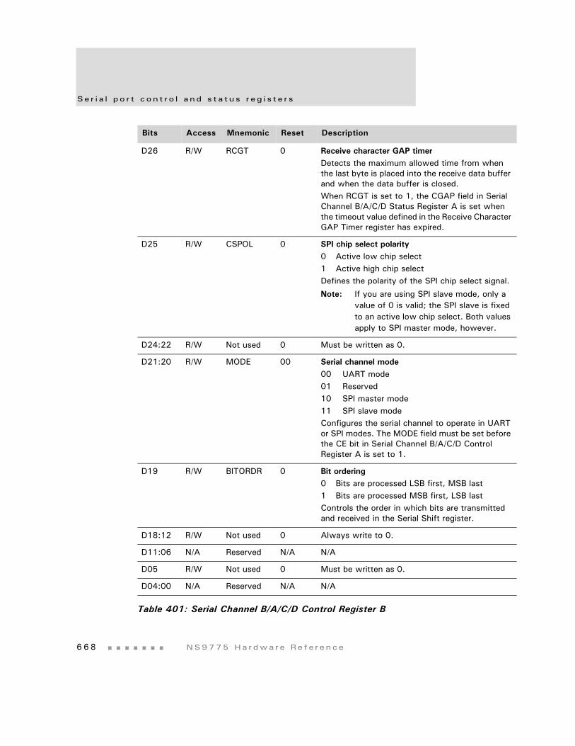
Se r i a l p o r t con t r o l a nd s t a t u s r e g i s t e r s
6 6 8 NS9775 Ha r dwa r e Re f e r ence
D26 R/W RCGT 0 Receive character GAP timerDetects the maximum allowed time from when the last byte is placed into the receive data buffer and when the data buffer is closed.When RCGT is set to 1, the CGAP field in Serial Channel B/A/C/D Status Register A is set when the timeout value defined in the Receive Character GAP Timer register has expired.
D25 R/W CSPOL 0 SPI chip select polarity0 Active low chip select1 Active high chip selectDefines the polarity of the SPI chip select signal.
Note: If you are using SPI slave mode, only a value of 0 is valid; the SPI slave is fixed to an active low chip select. Both values apply to SPI master mode, however.
D24:22 R/W Not used 0 Must be written as 0.
D21:20 R/W MODE 00 Serial channel mode00 UART mode01 Reserved10 SPI master mode11 SPI slave modeConfigures the serial channel to operate in UART or SPI modes. The MODE field must be set before the CE bit in Serial Channel B/A/C/D Control Register A is set to 1.
D19 R/W BITORDR 0 Bit ordering0 Bits are processed LSB first, MSB last1 Bits are processed MSB first, LSB lastControls the order in which bits are transmitted and received in the Serial Shift register.
D18:12 R/W Not used 0 Always write to 0.
D11:06 N/A Reserved N/A N/A
D05 R/W Not used 0 Must be written as 0.
D04:00 N/A Reserved N/A N/A
Bits Access Mnemonic Reset Description
Table 401: Serial Channel B/A/C/D Control Register B
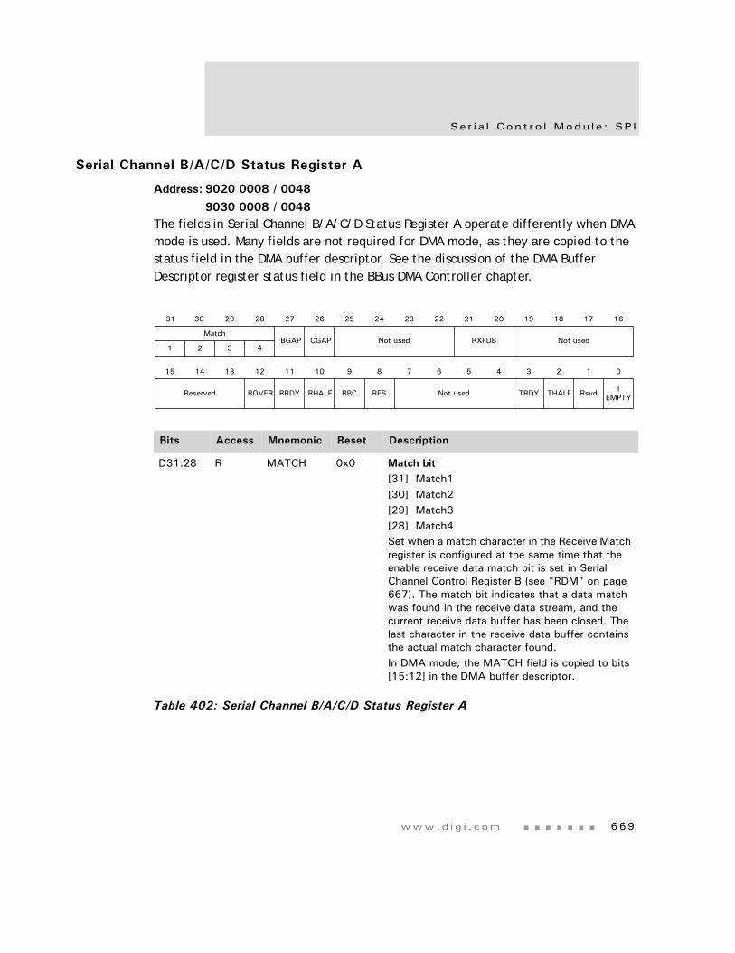
www.d i g i . com 669
Se r i a l Con t r o l Modu l e : SP I
Serial Channel B/A/C/D Status Register A
Address: 9020 0008 / 0048
9030 0008 / 0048The fields in Serial Channel B/A/C/D Status Register A operate differently when DMA mode is used. Many fields are not required for DMA mode, as they are copied to the status field in the DMA buffer descriptor. See the discussion of the DMA Buffer Descriptor register status field in the BBus DMA Controller chapter.
Bits Access Mnemonic Reset Description
D31:28 R MATCH 0x0 Match bit[31] Match1[30] Match2[29] Match3[28] Match4Set when a match character in the Receive Match register is configured at the same time that the enable receive data match bit is set in Serial Channel Control Register B (see "RDM" on page 667). The match bit indicates that a data match was found in the receive data stream, and the current receive data buffer has been closed. The last character in the receive data buffer contains the actual match character found. In DMA mode, the MATCH field is copied to bits [15:12] in the DMA buffer descriptor.
Table 402: Serial Channel B/A/C/D Status Register A
TEMPTY
13 12 11 10 9 8 7 6 5 4 3 2 1 015 14
31 29 28 27 26 25 24 23 22 21 20 19 18 17 1630
CGAPBGAP RXFDBMatch
Not used
THALF
1 2 3 4
Reserved ROVER RRDY RHALF RBC RFS TRDY Rsvd
Not used
Not used
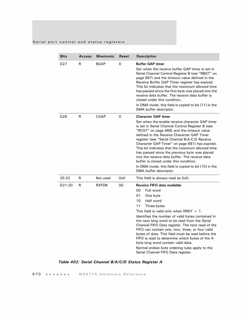
Se r i a l p o r t con t r o l a nd s t a t u s r e g i s t e r s
6 7 0 NS9775 Ha r dwa r e Re f e r ence
D27 R BGAP 0 Buffer GAP timerSet when the receive buffer GAP timer is set in Serial Channel Control Register B (see "RBGT" on page 667) and the timeout value defined in the Receive Buffer GAP Timer register has expired. This bit indicates that the maximum allowed time has passed since the first byte was placed into the receive data buffer. The receive data buffer is closed under this condition.In DMA mode, this field is copied to bit [11] in the DMA buffer descriptor.
D26 R CGAP 0 Character GAP timerSet when the enable receive character GAP timer is set in Serial Channel Control Register B (see "RCGT" on page 668) and the timeout value defined in the Receive Character GAP Timer register (see "Serial Channel B/A/C/D Receive Character GAP Timer" on page 681) has expired. This bit indicates that the maximum allowed time has passed since the previous byte was placed into the receive data buffer. The receive data buffer is closed under this condition.In DMA mode, this field is copied to bit [10] in the DMA buffer descriptor.
25:22 R Not used 0x0 This field is always read as 0x0.
D21:20 R RXFDB 00 Receive FIFO data available00 Full word01 One byte10 Half word11 Three bytesThis field is valid only when RRDY = 1.Identifies the number of valid bytes contained in the next long word to be read from the Serial Channel FIFO Data register. The next read of the FIFO can contain one, two, three, or four valid bytes of data. This field must be read before the FIFO is read to determine which bytes of the 4-byte long word contain valid data. Normal endian byte ordering rules apply to the Serial Channel FIFO Data register.
Bits Access Mnemonic Reset Description
Table 402: Serial Channel B/A/C/D Status Register A
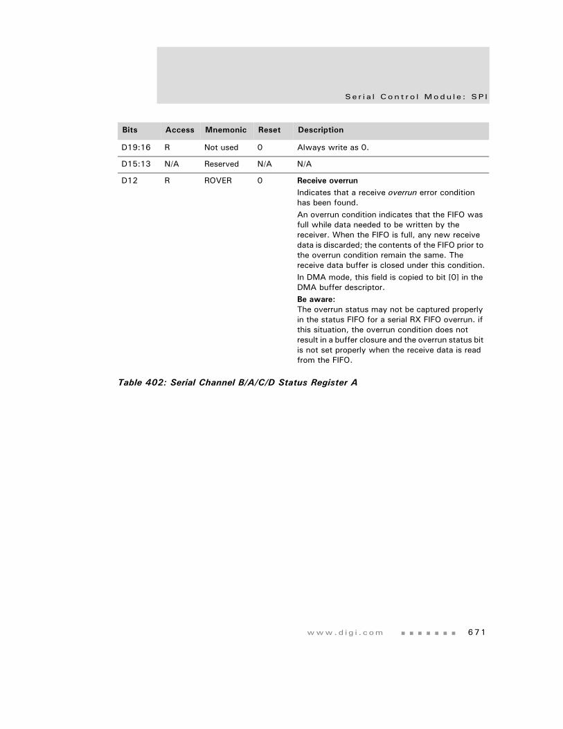
www.d i g i . com 671
Se r i a l Con t r o l Modu l e : SP I
D19:16 R Not used 0 Always write as 0.
D15:13 N/A Reserved N/A N/A
D12 R ROVER 0 Receive overrunIndicates that a receive overrun error condition has been found. An overrun condition indicates that the FIFO was full while data needed to be written by the receiver. When the FIFO is full, any new receive data is discarded; the contents of the FIFO prior to the overrun condition remain the same. The receive data buffer is closed under this condition.In DMA mode, this field is copied to bit [0] in the DMA buffer descriptor.Be aware: The overrun status may not be captured properly in the status FIFO for a serial RX FIFO overrun. if this situation, the overrun condition does not result in a buffer closure and the overrun status bit is not set properly when the receive data is read from the FIFO.
Bits Access Mnemonic Reset Description
Table 402: Serial Channel B/A/C/D Status Register A

Se r i a l p o r t con t r o l a nd s t a t u s r e g i s t e r s
6 7 2 NS9775 Ha r dwa r e Re f e r ence
D11 R RRDY 0 Receive register readyIndicates that data is available to be read from the FIFO Data register. Before reading the FIFO Data register, the RXFDB field in this (Serial Channel Status Register A) register (see D21:20) must be read to determine how many active bytes are available during the next read of the FIFO Data register.RRDY typically is used only in interrupt-driven applications; this field is not used for DMA operation. The RRDY status condition can be programmed to generate an interrupt by setting the corresponding IE bit in Serial Channel Control Register A.The RRDY bit is never active when the RBC (D09) bit is active. The RBC bit must be acknowledged by writing a 1 to the same bit position in this register to activate the RRDY bit. When the receiver is configured to operate in DMA mode, hardware automatically handles the interlock between RBC and RRDY.
D10 R RHALF 0 Receive FIFO half fullIndicates that the receive data FIFO contains at least 20 bytes (5 lines). RHALF typically is used only in interrupt-driven applications; this field is not used for DMA operation. The RHALF status condition can be programmed to generate an interrupt by setting the corresponding IE bit in Serial Channel Control Register A.
Bits Access Mnemonic Reset Description
Table 402: Serial Channel B/A/C/D Status Register A
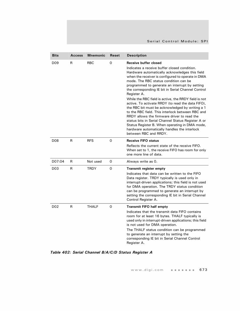
www.d i g i . com 673
Se r i a l Con t r o l Modu l e : SP I
D09 R RBC 0 Receive buffer closedIndicates a receive buffer closed condition. Hardware automatically acknowledges this field when the receiver is configured to operate in DMA mode. The RBC status condition can be programmed to generate an interrupt by setting the corresponding IE bit in Serial Channel Control Register A. While the RBC field is active, the RRDY field is not active. To activate RRDY (to read the data FIFO), the RBC bit must be acknowledged by writing a 1 to the RBC field. This interlock between RBC and RRDY allows the firmware driver to read the status bits in Serial Channel Status Register A or Status Register B. When operating in DMA mode, hardware automatically handles the interlock between RBC and RRDY.
D08 R RFS 0 Receive FIFO statusReflects the current state of the receive FIFO. When set to 1, the receive FIFO has room for only one more line of data.
D07:04 R Not used 0 Always write as 0.
D03 R TRDY 0 Transmit register emptyIndicates that data can be written to the FIFO Data register. TRDY typically is used only in interrupt-driven applications; this field is not used for DMA operation. The TRDY status condition can be programmed to generate an interrupt by setting the corresponding IE bit in Serial Channel Control Register A.
D02 R THALF 0 Transmit FIFO half emptyIndicates that the transmit data FIFO contains room for at least 16 bytes. THALF typically is used only in interrupt-driven applications; this field is not used for DMA operation. The THALF status condition can be programmed to generate an interrupt by setting the corresponding IE bit in Serial Channel Control Register A.
Bits Access Mnemonic Reset Description
Table 402: Serial Channel B/A/C/D Status Register A
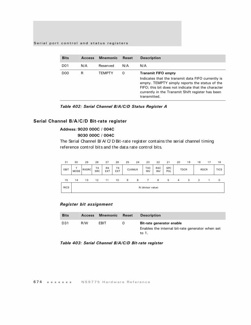
Se r i a l p o r t con t r o l a nd s t a t u s r e g i s t e r s
6 7 4 NS9775 Ha r dwa r e Re f e r ence
Serial Channel B/A/C/D Bit-rate register
Address: 9020 000C / 004C
9030 000C / 004CThe Serial Channel B/A/C/D Bit-rate register contains the serial channel timing reference control bits and the data rate control bits.
Register bit assignment
D01 N/A Reserved N/A N/A
D00 R TEMPTY 0 Transmit FIFO emptyIndicates that the transmit data FIFO currently is empty. TEMPTY simply reports the status of the FIFO; this bit does not indicate that the character currently in the Transmit Shift register has been transmitted.
Bits Access Mnemonic Reset Description
Table 402: Serial Channel B/A/C/D Status Register A
Bits Access Mnemonic Reset Description
D31 R/W EBIT 0 Bit-rate generator enableEnables the internal bit-rate generator when set to 1.
Table 403: Serial Channel B/A/C/D Bit-rate register
13 12 11 10 9 8 7 6 5 4 3 2 1 015 14
RICS N (divisor value)
31 29 28 27 26 25 24 23 22 21 20 19 18 17 1630
RXSRC TXSRC
TXEXT
RXEXT CLKMUX TXC
INVRXCINV
SPCPOL TDCR TICSEBIT T
MODE RDCR
www.d i g i . com 675
Se r i a l Con t r o l Modu l e : SP I
D30 R/W TMODE 0 Timing modeMust be set to 1. Use the additional timing configuration provided by the TDCR and RDCR fields (D[20:19] and D[18:17] in this register) to configure the channel for 1x, 8x, 16x, or 32x mode.
D29 R/W RXSRC 0 Receive timing source0 Internal1 External (input using GPIO pin)Controls the source of the receiver clock. The receive clock can be provided by an internal source selected using the RICS field (see D15).As an alternative, the receiver clock can be provided by an input on GPIO pins gpio[6], gpio[14], gpio[22], and gpio[26] for serial ports B, A, C, and D, respectively.For SPI master and slave, set to 0 for internal.
D28 R/W TXSRC 0 Transmit clock source0 Internal1 External (input using GPIO pin)Controls the source of the transmitter clock. The transmitter clock can be provided by an internal source selected using the TICS field (see D16).As an alternative, the transmitter clock can be provided by an input on GPIO pins gpio[7], gpio[15], gpio[23], and gpio[27] for serial ports B, A, C, and D, respectively.For SPI master and slave, set to 0 for internal.
D27 R/W RXEXT 0 Drive receive clock external0 Disable1 EnableEnables the receiver clock to be driven on GPIO pins gpio[6], gpio[14], gpio[22], and gpio[26] for serial ports B, A, C, and D, respectively.For SPI master and slave, set to 0 to disable.
Bits Access Mnemonic Reset Description
Table 403: Serial Channel B/A/C/D Bit-rate register
Se r i a l p o r t con t r o l a nd s t a t u s r e g i s t e r s
6 7 6 NS9775 Ha r dwa r e Re f e r ence
D26 R/W TXEXT 0 Drive transmit clock external0 Disable1 EnableEnables the transmitter clock to be driven on GPIO pins gpio[7], gpio[15], gpio[23], gpio[27] for serial ports B, A, C, and D, respectively.For SPI master mode, set to 1 to enable.For SPI slave mode, set to 0 to disable.
D25:24 R/W CLKMUX 00 Bit-rate generator clock sourceControls the bit-rate generator clock source. The bit-rate generator can be configured to use one of four clock sources:00 x1_sys_osc/M (see Table 396, “Bit-rate
generation clock sources,” on page 657 for more information). This selection is not valid when the PLLBP field in the PLL Configuration register is set to 1.
01 BCLKThis is the recommended setting for SPI master and slave operation.
10 Input clock defined by external receive clock on GPIO pins gpio[6], gpio[14], gpio[22], and gpio[26] for serial ports B, A, C, and D, respectively.
11 Input clock defined by external transmit clock on GPIO pins gpio[7], gpio[15], gpio[23], and gpio[27] for serial ports B, A, C, and D, respectively.
D23 R/W TXCINV 0 Transmit clock invertControls the relationship between transmit clock and transmit data:
When set to 0, transmit data changes relative to the falling edge transition of the transmit clock. Use 0 for SPI modes 0 and 3.
When set to 1, transmit data changes relative to the rising edge transition of the transmit clock. Use 1 for SPI modes 1 and 2.
Bits Access Mnemonic Reset Description
Table 403: Serial Channel B/A/C/D Bit-rate register
www.d i g i . com 677
Se r i a l Con t r o l Modu l e : SP I
D22 R/W RXCINV 0 Receive clock invertControls the relationship between receive clock and receive data:
When set to 0, the receive data input is sampled at the rising edge transition of the receive clock. Use 0 for SPI modes 0 and 3.
When set to 1, the receive data input is sampled at the falling edge transition of the receive clock. Use 1 for SPI modes 1 and 2.
D21 R/W SPCPOL 0/1 SPI transmit polarity0 Idle high operation; use this value for SPI
modes 1 and 31 Idle low operation; use this value for SPI
modes 0 and 2Defines the idle polarity of the SPI transmit clock.
D20:19 R/W TDCR 00 Transmit clock divide rate00 1x clock mode (only NRZ or NRZI allowed)01 8x clock mode10 16x clock mode11 32x clock modeDetermines the divide ratio for the transmitter clock.If the DPLL is not used, use the 1x clock mode value (00). When DPLL is used in the application, selecting TDCR/RDCR is a function of the transmitter encoding. The NRZ and NRZI modes can use the 1x configuration; all other encoding must use 8x, 16x, or 32x configuration mode. The 8x configuration provides the highest possible data rate; the 32x mode provides the highest possible resolution.The TMODE bit in this register is maintained for NET+Arm family backward compatibility. When setting the TDCR or RDCR register to a non-zero value, the TMODE bit must be set to 1. When TMODE, TDCR, and RDCR are all set to 0, the port defaults to 16x mode of operation.
Bits Access Mnemonic Reset Description
Table 403: Serial Channel B/A/C/D Bit-rate register
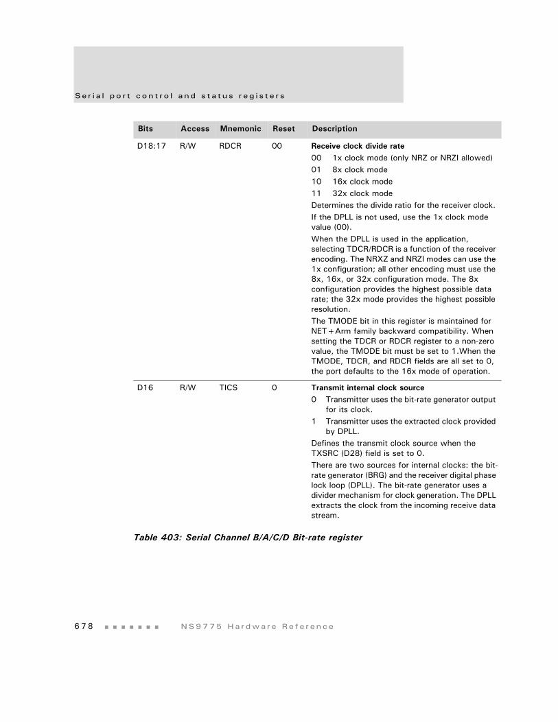
Se r i a l p o r t con t r o l a nd s t a t u s r e g i s t e r s
6 7 8 NS9775 Ha r dwa r e Re f e r ence
D18:17 R/W RDCR 00 Receive clock divide rate00 1x clock mode (only NRZ or NRZI allowed)01 8x clock mode10 16x clock mode11 32x clock modeDetermines the divide ratio for the receiver clock. If the DPLL is not used, use the 1x clock mode value (00). When the DPLL is used in the application, selecting TDCR/RDCR is a function of the receiver encoding. The NRXZ and NRZI modes can use the 1x configuration; all other encoding must use the 8x, 16x, or 32x configuration mode. The 8x configuration provides the highest possible data rate; the 32x mode provides the highest possible resolution.The TMODE bit in this register is maintained for NET+Arm family backward compatibility. When setting the TDCR or RDCR register to a non-zero value, the TMODE bit must be set to 1.When the TMODE, TDCR, and RDCR fields are all set to 0, the port defaults to the 16x mode of operation.
D16 R/W TICS 0 Transmit internal clock source0 Transmitter uses the bit-rate generator output
for its clock.1 Transmitter uses the extracted clock provided
by DPLL.Defines the transmit clock source when the TXSRC (D28) field is set to 0. There are two sources for internal clocks: the bit-rate generator (BRG) and the receiver digital phase lock loop (DPLL). The bit-rate generator uses a divider mechanism for clock generation. The DPLL extracts the clock from the incoming receive data stream.
Bits Access Mnemonic Reset Description
Table 403: Serial Channel B/A/C/D Bit-rate register
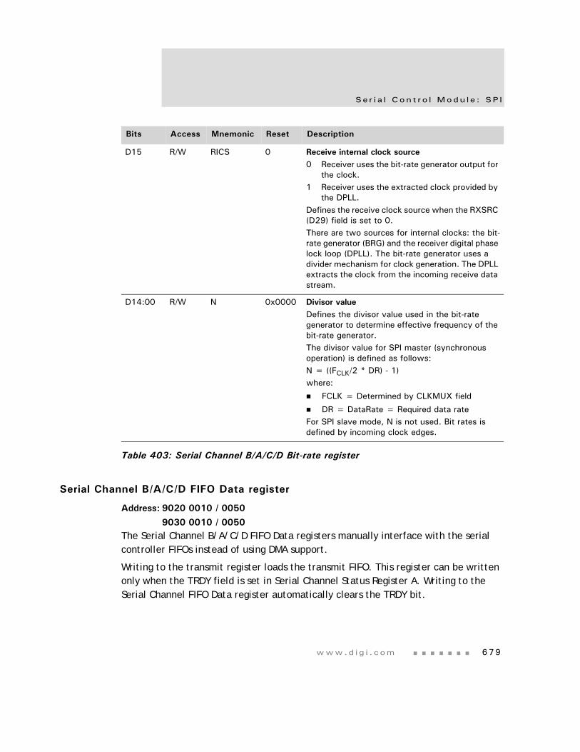
www.d i g i . com 679
Se r i a l Con t r o l Modu l e : SP I
Serial Channel B/A/C/D FIFO Data register
Address: 9020 0010 / 0050
9030 0010 / 0050The Serial Channel B/A/C/D FIFO Data registers manually interface with the serial controller FIFOs instead of using DMA support.
Writing to the transmit register loads the transmit FIFO. This register can be written only when the TRDY field is set in Serial Channel Status Register A. Writing to the Serial Channel FIFO Data register automatically clears the TRDY bit.
D15 R/W RICS 0 Receive internal clock source0 Receiver uses the bit-rate generator output for
the clock.1 Receiver uses the extracted clock provided by
the DPLL.Defines the receive clock source when the RXSRC (D29) field is set to 0. There are two sources for internal clocks: the bit-rate generator (BRG) and the receiver digital phase lock loop (DPLL). The bit-rate generator uses a divider mechanism for clock generation. The DPLL extracts the clock from the incoming receive data stream.
D14:00 R/W N 0x0000 Divisor valueDefines the divisor value used in the bit-rate generator to determine effective frequency of the bit-rate generator. The divisor value for SPI master (synchronous operation) is defined as follows:N = ((FCLK/2 * DR) - 1)where:
FCLK = Determined by CLKMUX field
DR = DataRate = Required data rateFor SPI slave mode, N is not used. Bit rates is defined by incoming clock edges.
Bits Access Mnemonic Reset Description
Table 403: Serial Channel B/A/C/D Bit-rate register
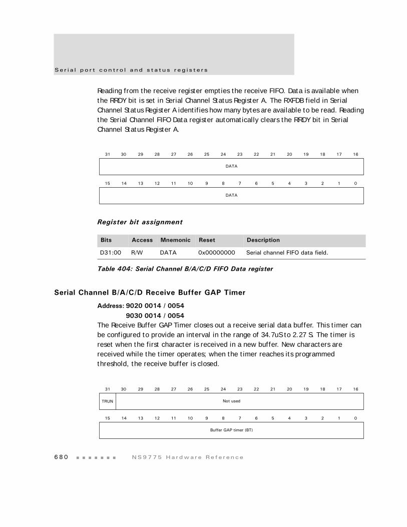
Se r i a l p o r t con t r o l a nd s t a t u s r e g i s t e r s
6 8 0 NS9775 Ha r dwa r e Re f e r ence
Reading from the receive register empties the receive FIFO. Data is available when the RRDY bit is set in Serial Channel Status Register A. The RXFDB field in Serial Channel Status Register A identifies how many bytes are available to be read. Reading the Serial Channel FIFO Data register automatically clears the RRDY bit in Serial Channel Status Register A.
Register bit assignment
Serial Channel B/A/C/D Receive Buffer GAP Timer
Address: 9020 0014 / 0054
9030 0014 / 0054The Receive Buffer GAP Timer closes out a receive serial data buffer. This timer can be configured to provide an interval in the range of 34.7uS to 2.27 S. The timer is reset when the first character is received in a new buffer. New characters are received while the timer operates; when the timer reaches its programmed threshold, the receive buffer is closed.
Bits Access Mnemonic Reset Description
D31:00 R/W DATA 0x00000000 Serial channel FIFO data field.
Table 404: Serial Channel B/A/C/D FIFO Data register
13 12 11 10 9 8 7 6 5 4 3 2 1 015 14
31 29 28 27 26 25 24 23 22 21 20 19 18 17 1630
DATA
DATA
13 12 11 10 9 8 7 6 5 4 3 2 1 015 14
31 29 28 27 26 25 24 23 22 21 20 19 18 17 1630
Not used
Buffer GAP timer (BT)
TRUN
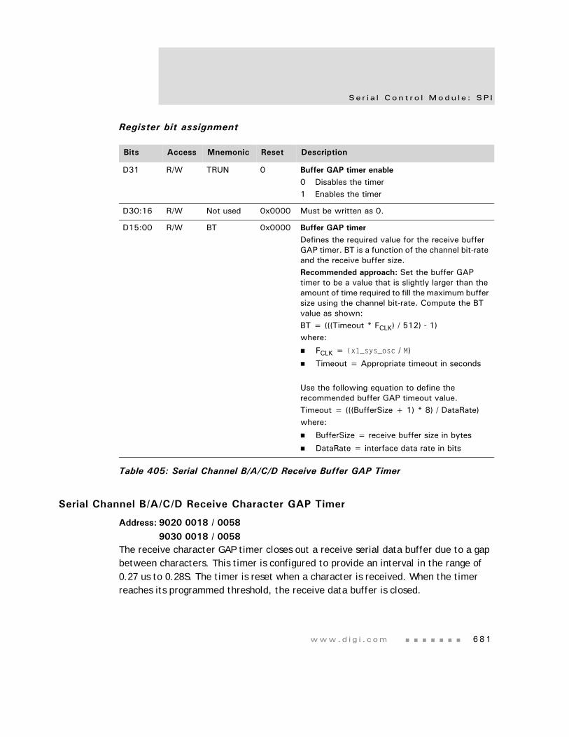
www.d i g i . com 681
Se r i a l Con t r o l Modu l e : SP I
Register bit assignment
Serial Channel B/A/C/D Receive Character GAP Timer
Address: 9020 0018 / 0058
9030 0018 / 0058The receive character GAP timer closes out a receive serial data buffer due to a gap between characters. This timer is configured to provide an interval in the range of 0.27 us to 0.28S. The timer is reset when a character is received. When the timer reaches its programmed threshold, the receive data buffer is closed.
Bits Access Mnemonic Reset Description
D31 R/W TRUN 0 Buffer GAP timer enable0 Disables the timer1 Enables the timer
D30:16 R/W Not used 0x0000 Must be written as 0.
D15:00 R/W BT 0x0000 Buffer GAP timerDefines the required value for the receive buffer GAP timer. BT is a function of the channel bit-rate and the receive buffer size. Recommended approach: Set the buffer GAP timer to be a value that is slightly larger than the amount of time required to fill the maximum buffer size using the channel bit-rate. Compute the BT value as shown:BT = (((Timeout * FCLK) / 512) - 1)where:
FCLK = (x1_sys_osc / M)
Timeout = Appropriate timeout in seconds
Use the following equation to define the recommended buffer GAP timeout value. Timeout = (((BufferSize + 1) * 8) / DataRate)where:
BufferSize = receive buffer size in bytes
DataRate = interface data rate in bits
Table 405: Serial Channel B/A/C/D Receive Buffer GAP Timer
Se r i a l p o r t con t r o l a nd s t a t u s r e g i s t e r s
6 8 2 NS9775 Ha r dwa r e Re f e r ence
Register bit assignment
Bits Access Mnemonic Reset Description
D31 R/W TRUN 0x0 Character GAP timer enable0 Disables the timer1 Enables the timer
D30:20 R/W Not used 0x000 Must be written as 0.
D19:00 CT CT 0x00000 Character GAP timerDefines the required value for the receive character GAP timer. Compute the CT value as shown:CT = (((Timeout * FCLK)/4) - 1)where:
FCLK = (x1_sys_osc / M)
Timeout = Appropriate timeout in seconds
Use the following equation to define the recommended character GAP timeout value:Timeout = (NumBitGap / DataRate)where:
NumBitGap = The number of bits in a character plus any start, stop, or parity bits.
DataRate = Interface data rate in bits per second.
Table 406: Serial Channel B/A/C/D Receive Character GAP Timer
13 12 11 10 9 8 7 6 5 4 3 2 1 015 14
31 29 28 27 26 25 24 23 22 21 20 19 18 17 1630
Not used
Character GAP timer (CT)
TRUN Character GAP timer (CT)
www.d i g i . com 683
Se r i a l Con t r o l Modu l e : SP I
Serial Channel B/A/C/D Receive Match register
Address: 9020 001C / 005C
9030 001C / 005CThe Serial Channel B/A/C/D Receive Match register contains the four receive data match bytes used in SPI mode.
Register bit assignment
Bits Access Mnemonic Reset Description
D31:24 R/W RDMB1 0x00 Receive data match byte1
D23:16 R/W RDMB2 0x00 Receive data match byte2
D15:08 R/W RDMB3 0x00 Receive data match byte3
D07:00 R/W RDMB4 0x00 Receive data match byte4
Table 407: Serial Channel B/A/C/D Receive Match register
RDMB4
13 12 11 10 9 8 7 6 5 4 3 2 1 015 14
31 29 28 27 26 25 24 23 22 21 20 19 18 17 1630
RDMB1
RDMB3
RDMB2
Se r i a l p o r t con t r o l a nd s t a t u s r e g i s t e r s
6 8 4 NS9775 Ha r dwa r e Re f e r ence
Serial Channel B/A/C/D Receive Match MASK register
Address: 9020 0020 / 0060
9030 0020 / 0060The Serial Channel B/A/C/D Receive Match MASK register contains the four receive match mask bytes that specify which bits in the Receive Match Data register should not be included in the match comparison. To mask a bit in the match comparison function, place a 1 in the same bit position in this register.
Register bit assignment
Bits Access Mnemonic Reset Description
D31:24 R/W RMMB1 0x00 Receive mask match byte1
23:16 R/W RMMB2 0x00 Receive mask match byte2
15:08 R/W RMMB3 0x00 Receive mask match byte3
07:00 R/W RMMB4 0x00 Receive mask match byte4
Table 408: Serial Channel B/A/C/D Receive Match MASK register
RMMB4
13 12 11 10 9 8 7 6 5 4 3 2 1 015 14
31 29 28 27 26 25 24 23 22 21 20 19 18 17 1630
RMMB1
RMMB3
RMMB2
685
IEEE 1284 Peripheral ControllerC H A P T E R 1 5
The IEEE 1284 peripheral port supports compatibility mode, nibble mode, byte mode, and ECP mode of operations as a peripheral device. The IEEE 1284 port does not support EPP/mode daisy chain or multiplexer operations.
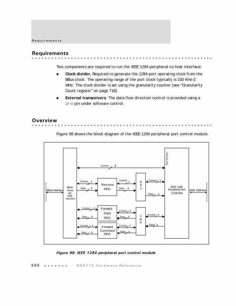
Requ i r emen t s
6 8 6 NS9775 Ha r dwa r e Re f e r ence
Requirements
Two components are required to run the IEEE 1284 peripheral-to-host interface:
Clock divider. Required to generate the 1284-port operating clock from the BBus clock. The operating range of the port clock typically is 100 KHz–2 MHz. The clock divider is set using the granularity counter (see "Granularity Count register" on page 718).
External transceivers. The data flow direction control is provided using a GPIO pin under software control.
Overview
Figure 98 shows the block diagram of the IEEE 1284 peripheral port control module.
Figure 98: IEEE 1284 peripheral port control module
Rev erseFIFO
ForwardDataFIFO
ForwardCommand
FIFO
BBUSSlaveand
DMAInterface
REV
FWD
Hos
tInt
erfa
ce
BBus Interface IEEE 1284 BusIEEE 1284
Peripheral PortController
Control
Control
Data
21
4
8
Control 2
Data 8
Control
Data 8
2
Control 4
Data 8
Control 2
Data 8Control 2
Data 8Control 2
Data 8Data 8
Control 4
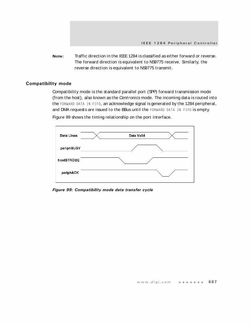
www.d i g i . com 687
I EEE 1284 Pe r i p h e r a l Con t r o l l e r
Note: Traffic direction in the IEEE 1284 is classified as either forward or reverse. The forward direction is equivalent to NS9775 receive. Similarly, the reverse direction is equivalent to NS9775 transmit.
Compatibility mode
Compatibility mode is the standard parallel port (SPP) forward transmission mode (from the host), also known as the Centronics mode. The incoming data is routed into the FORWARD DATA IN FIFO, an acknowledge signal is generated by the 1284 peripheral, and DMA requests are issued to the BBus until the FORWARD DATA IN FIFO is empty.
Figure 99 shows the timing relationship on the port interface.
Figure 99: Compatibility mode data transfer cycle
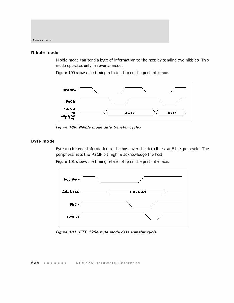
Ove r v i ew
6 8 8 NS9775 Ha r dwa r e Re f e r ence
Nibble mode
Nibble mode can send a byte of information to the host by sending two nibbles. This mode operates only in reverse mode.
Figure 100 shows the timing relationship on the port interface.
Figure 100: Nibble mode data transfer cycles
Byte mode
Byte mode sends information to the host over the data lines, at 8 bits per cycle. The peripheral sets the PtrClk bit high to acknowledge the host.
Figure 101 shows the timing relationship on the port interface.
Figure 101: IEEE 1284 byte mode data transfer cycle
www.d i g i . com 689
I EEE 1284 Pe r i p h e r a l Con t r o l l e r
ECP mode
ECP (extended capability port) mode provides a high performance bi-directional communication path between the host and the peripheral. The ECP protocol provides two cycle types in both the forward and reverse directions: data cycles and command cycles.
Two types of command cycles are supported by the IEEE peripheral: run length count and channel address. The transfer direction is controlled by the host until a ReverseRequest signal is issued by the host. The peripheral can set the PeriphRequest signal low to indicate that reverse data is available.
Run_Length_Encoding (RLE) data compression enables real time data compression that can achieve ratios up to 64:1. NS9775 uses RLE decoding to enable large raster images with large strings of identical data to be transferred to system memory.
Forward transfer cycles
Be advised: In forward ECP mode, the PeriphAck signal indicates to the host the ability of the peripheral to accept data. At event #6 of the negotiation process, the NS9775 indicates to the host that it cannot accept data and holds its PeriphAck signal high for approximately 1200ns.
To differentiate the data cycles from the command cycles, the host sets the HostAck signal at the beginning of the cycle. When HostAck is asserted low, a command cycle is occurring and the data represents either an RLE count or a channel address. Bit 7 of the data byte indicates what is represented:
If bit 7is 0, the data is an RLE count and (bits[6:0] + 1) versions of the subsequent byte are placed into the appropriate forward FIFO based on the value of HostAck while it is being transferred.
If bit 7 is 1, the data is a channel address (0–127), and bits [6:0] are written into the Forward Address register ("Forward Address register" on page 719).
Figure 102 shows a data cycle followed by a command cycle.
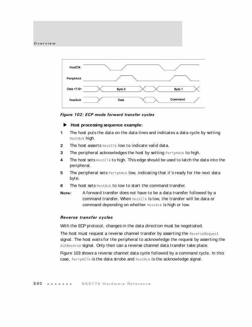
Ove r v i ew
6 9 0 NS9775 Ha r dwa r e Re f e r ence
Figure 102: ECP mode forward transfer cycles
Host processing sequence example:
1 The host puts the data on the data lines and indicates a data cycle by setting HostAck high.
2 The host asserts HostClk low to indicate valid data.
3 The peripheral acknowledges the host by setting PeriphAck to high.
4 The host sets HostClk to high. This edge should be used to latch the data into the peripheral.
5 The peripheral sets PeriphAck low, indicating that it’s ready for the next data byte.
6 The host sets HostAck to low to start the command transfer.
Note: A forward transfer does not have to be a data transfer followed by a command transfer. When HostClk is low, the transfer will be data or command depending on whether HostAck is high or low.
Reverse transfer cycles
With the ECP protocol, changes in the data direction must be negotiated.
The host must request a reverse channel transfer by asserting the ReverseRequest signal. The host waits for the peripheral to acknowledge the request by asserting the AckReverse signal. Only then can a reverse channel data transfer take place.
Figure 103 shows a reverse channel data cycle followed by a command cycle. In this case, PeriphClk is the data strobe and HostAck is the acknowledge signal.
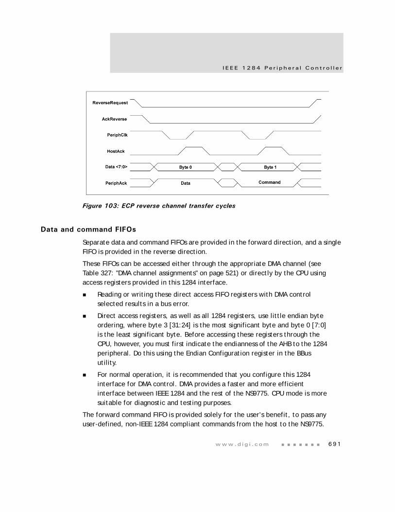
www.d i g i . com 691
I EEE 1284 Pe r i p h e r a l Con t r o l l e r
Figure 103: ECP reverse channel transfer cycles
Data and command FIFOs
Separate data and command FIFOs are provided in the forward direction, and a single FIFO is provided in the reverse direction.
These FIFOs can be accessed either through the appropriate DMA channel (see Table 327: "DMA channel assignments" on page 521) or directly by the CPU using access registers provided in this 1284 interface.
Reading or writing these direct access FIFO registers with DMA control selected results in a bus error.
Direct access registers, as well as all 1284 registers, use little endian byte ordering, where byte 3 [31:24] is the most significant byte and byte 0 [7:0] is the least significant byte. Before accessing these registers through the CPU, however, you must first indicate the endianness of the AHB to the 1284 peripheral. Do this using the Endian Configuration register in the BBus utility.
For normal operation, it is recommended that you configure this 1284 interface for DMA control. DMA provides a faster and more efficient interface between IEEE 1284 and the rest of the NS9775. CPU mode is more suitable for diagnostic and testing purposes.
The forward command FIFO is provided solely for the user’s benefit, to pass anyuser-defined, non-IEEE 1284 compliant commands from the host to the NS9775.
Ove r v i ew
6 9 2 NS9775 Ha r dwa r e Re f e r ence
Because the NS9775 functions only as a slave, it is not necessary to provide the capability of driving any non-IEEE 1284 compliant commands back to the host.
Important: The 1284 commands are not designed to be stored and passed along. To store a non-IEEE 1284 command in the forward command FIFO, send an RLE command of count one (0x0), followed by the command you want to send. Both bytes must be transferred while HostAck is low and bit[14] of the IEEE 1284 General Configuration register (see page 695) is set to 0.
IEEE 1284 negotiation
The negotiation process is a mechanism by which the host determines the capabilities of the attached peripheral. The module can be programmed to interrupt the software when the host begins negotiation. The module automatically completes negotiation into byte, nibble, and ECP modes. The host uses an extensibility byte to communicate to the module which mode is being negotiated into.
Warning: During a negotiation into either nibble or byte mode, the behavior of the pError signal driven by the NS9775 is out of compliance with the IEEE 1284 standard. The pError signal does not match the value of nFault at event #6 of the negotiation process.
Table 409 defines the extensibility byte values.
Extensibility byte Definition Description
1000 0000 Reserved Reserved
0100 0000 Reserved Reserved
0011 0000 Request ECP mode with RLE
0001 0000 Request ECP mode without RLE
0000 1000 Reserved Reserved
0000 0100 Request device ID using nibble mode
Receive the device ID a nibble at a time across the status lines.
0000 0101 Request device ID using byte mode
Receive the device ID a byte at a time across the data lines.
0001 0100 Request device ID using ECP mode without RLE
Receive device ID without ECP data compression.
Table 409: Extensibility byte values
www.d i g i . com 693
I EEE 1284 Pe r i p h e r a l Con t r o l l e r
The NS9775 directly supports RLE compression. The device ID can be returned in any supported reverse channel mode. The device ID is a length field followed by a string of ASCII characters that define the peripheral’s characters and/or capabilities.
BBus slave and DMA interface
The BBus slave and DMA interface module controls accesses from the BBus to the IEEE peripheral. The interface can operate in two modes: DMA and CPU.
In DMA mode, three BBus DMA channels are used for forward data and forward command traffic, and all reverse traffic.
In CPU mode, the CPU can access the forward data, forward command, and reverse FIFOs directly.
BBus slave and DMA interface register map
The IEEE 1284 module uses the control and status registers listed in Table 410.
All configuration registers must be accessed as 32-bit words and as single accesses only. No bursting is allowed.
0011 0100 Request device ID using ECP mode with RLE
Receive device ID with ECP data compression.
0000 0010 Reserved Reserved
0000 0001 Byte mode reverse channel transfer
0000 0000 Nibble mode reverse channel transfer
Extensibility byte Definition Description
Table 409: Extensibility byte values
Address Register Description
9040 0000 GenConfig General Configuration register
Table 410: 1284 Control and Status registers
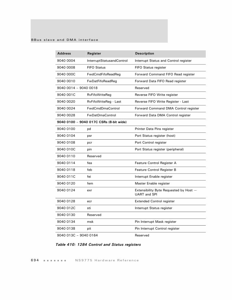
BBus s l a v e a nd DMA i n t e r f a ce
6 9 4 NS9775 Ha r dwa r e Re f e r ence
9040 0004 InterruptStatusandControl Interrupt Status and Control register
9040 0008 FIFO Status FIFO Status register
9040 000C FwdCmdFifoReadReg Forward Command FIFO Read register
9040 0010 FwDatFifoReadReg Forward Data FIFO Read register
9040 0014 – 9040 0018 Reserved
9040 001C RvFifoWriteReg Reverse FIFO Write register
9040 0020 RvFifoWriteReg - Last Reverse FIFO Write Register - Last
9040 0024 FwdCmdDmaControl Forward Command DMA Control register
9040 0028 FwDatDmaControl Forward Data DMA Control register
9040 0100 – 9040 017C CSRs (8-bit wide)
9040 0100 pd Printer Data Pins register
9040 0104 psr Port Status register (host)
9040 0108 pcr Port Control register
9040 010C pin Port Status register (peripheral)
9040 0110 Reserved
9040 0114 fea Feature Control Register A
9040 0118 feb Feature Control Register B
9040 011C fei Interrupt Enable register
9040 0120 fem Master Enable register
9040 0124 exr Extensibility Byte Requested by Host — UART and SPI
9040 0128 ecr Extended Control register
9040 012C sti Interrupt Status register
9040 0130 Reserved
9040 0134 msk Pin Interrupt Mask register
9040 0138 pit Pin Interrupt Control register
9040 013C – 9040 0164 Reserved
Address Register Description
Table 410: 1284 Control and Status registers
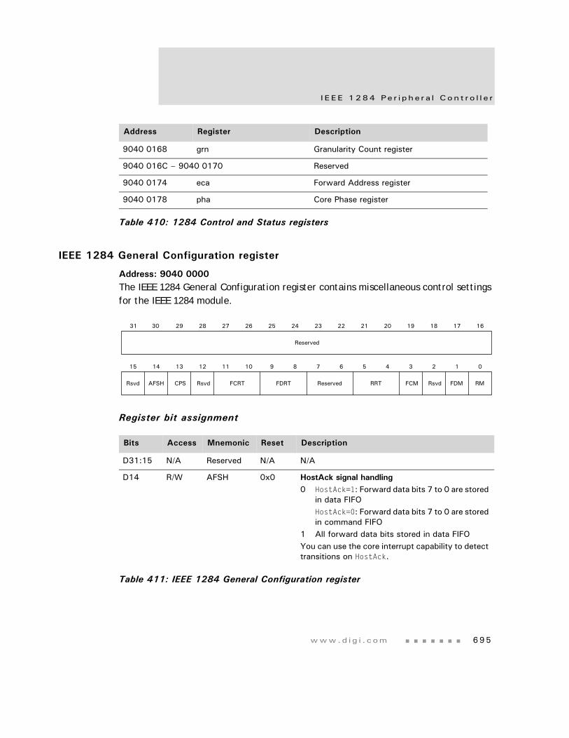
www.d i g i . com 695
I EEE 1284 Pe r i p h e r a l Con t r o l l e r
IEEE 1284 General Configuration register
Address: 9040 0000The IEEE 1284 General Configuration register contains miscellaneous control settings for the IEEE 1284 module.
Register bit assignment
9040 0168 grn Granularity Count register
9040 016C – 9040 0170 Reserved
9040 0174 eca Forward Address register
9040 0178 pha Core Phase register
Address Register Description
Table 410: 1284 Control and Status registers
Bits Access Mnemonic Reset Description
D31:15 N/A Reserved N/A N/A
D14 R/W AFSH 0x0 HostAck signal handling0 HostAck=1: Forward data bits 7 to 0 are stored
in data FIFOHostAck=0: Forward data bits 7 to 0 are stored in command FIFO
1 All forward data bits stored in data FIFO You can use the core interrupt capability to detect transitions on HostAck.
Table 411: IEEE 1284 General Configuration register
CPS Rsvd FCRT FDRT Reserved RRT FCM Rsvd FDM RM
13 12 11 10 9 8 7 6 5 4 3 2 1 015 14
31 29 28 27 26 25 24 23 22 21 20 19 18 17 1630
Reserved
Rsvd AFSH
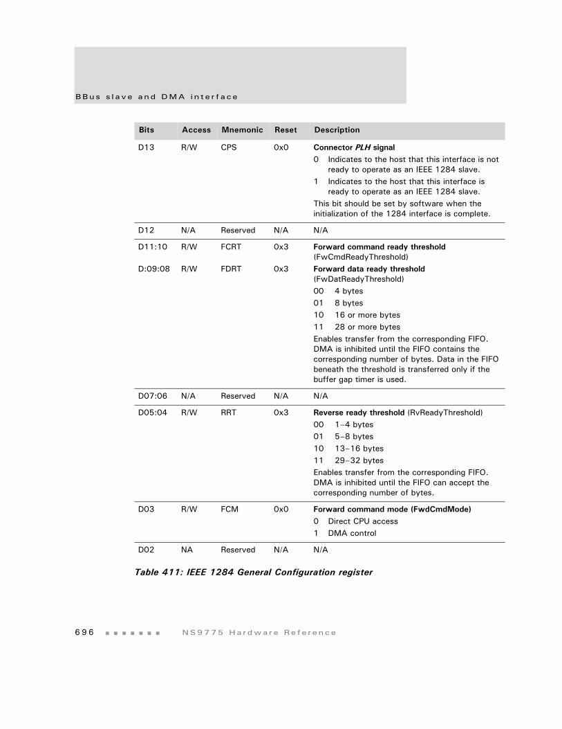
BBus s l a v e a nd DMA i n t e r f a ce
6 9 6 NS9775 Ha r dwa r e Re f e r ence
D13 R/W CPS 0x0 Connector PLH signal0 Indicates to the host that this interface is not
ready to operate as an IEEE 1284 slave.1 Indicates to the host that this interface is
ready to operate as an IEEE 1284 slave.This bit should be set by software when the initialization of the 1284 interface is complete.
D12 N/A Reserved N/A N/A
D11:10
D:09:08
R/W
R/W
FCRT
FDRT
0x3
0x3
Forward command ready threshold (FwCmdReadyThreshold)Forward data ready threshold (FwDatReadyThreshold)00 4 bytes01 8 bytes10 16 or more bytes11 28 or more bytesEnables transfer from the corresponding FIFO. DMA is inhibited until the FIFO contains the corresponding number of bytes. Data in the FIFO beneath the threshold is transferred only if the buffer gap timer is used.
D07:06 N/A Reserved N/A N/A
D05:04 R/W RRT 0x3 Reverse ready threshold (RvReadyThreshold)00 1–4 bytes01 5–8 bytes10 13–16 bytes11 29–32 bytesEnables transfer from the corresponding FIFO. DMA is inhibited until the FIFO can accept the corresponding number of bytes.
D03 R/W FCM 0x0 Forward command mode (FwdCmdMode)0 Direct CPU access1 DMA control
D02 NA Reserved N/A N/A
Bits Access Mnemonic Reset Description
Table 411: IEEE 1284 General Configuration register
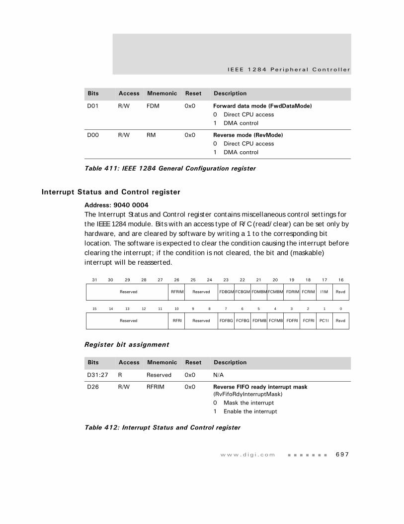
www.d i g i . com 697
I EEE 1284 Pe r i p h e r a l Con t r o l l e r
Interrupt Status and Control register
Address: 9040 0004The Interrupt Status and Control register contains miscellaneous control settings for the IEEE 1284 module. Bits with an access type of R/C (read/clear) can be set only by hardware, and are cleared by software by writing a 1 to the corresponding bit location. The software is expected to clear the condition causing the interrupt before clearing the interrupt; if the condition is not cleared, the bit and (maskable) interrupt will be reasserted.
Register bit assignment
D01 R/W FDM 0x0 Forward data mode (FwdDataMode)0 Direct CPU access1 DMA control
D00 R/W RM 0x0 Reverse mode (RevMode)0 Direct CPU access1 DMA control
Bits Access Mnemonic Reset Description
Table 411: IEEE 1284 General Configuration register
Bits Access Mnemonic Reset Description
D31:27 R Reserved 0x0 N/A
D26 R/W RFRIM 0x0 Reverse FIFO ready interrupt mask (RvFifoRdyInterruptMask)0 Mask the interrupt1 Enable the interrupt
Table 412: Interrupt Status and Control register
RFRI FDFBG FCFBG FDFMB FCFMB FDFRI FCFRI PC1I Rsvd
13 12 11 10 9 8 7 6 5 4 3 2 1 015 14
31 29 28 27 26 25 24 23 22 21 20 19 18 17 1630
RFRIM FDBGM FCBGM FDMBM FCMBM FDRIM FCRIM I1M RsvdReserved
Reserved
Reserved
Reserved
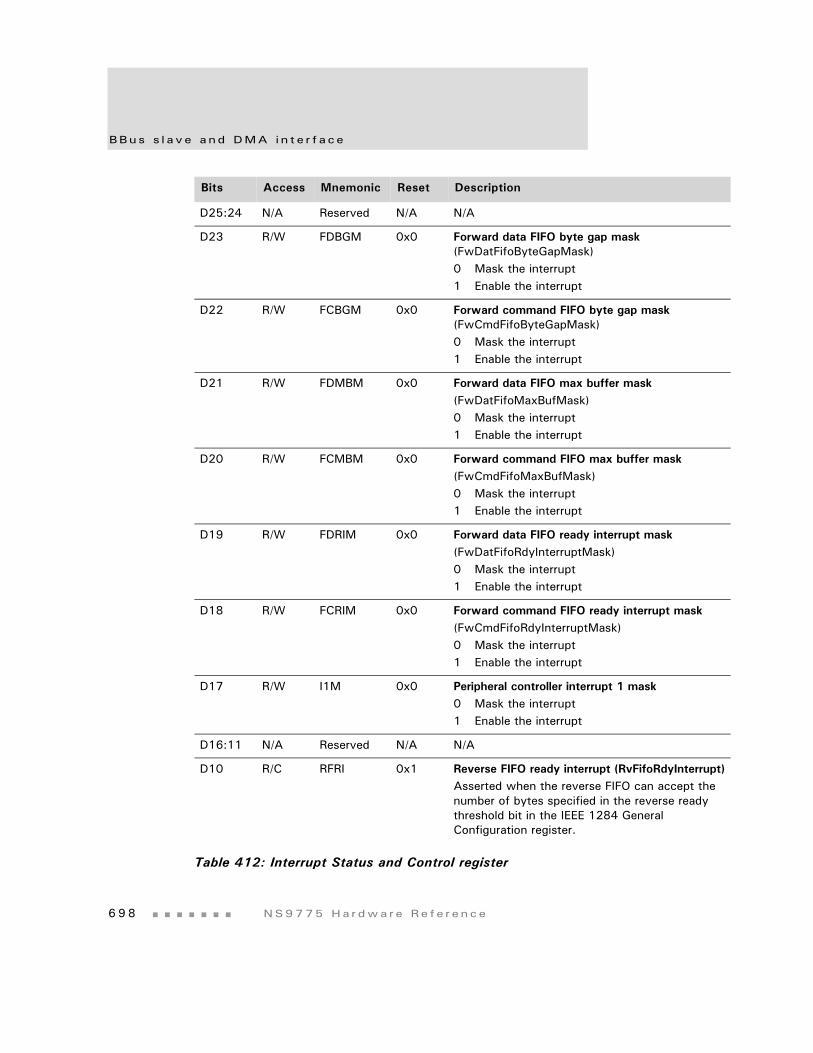
BBus s l a v e a nd DMA i n t e r f a ce
6 9 8 NS9775 Ha r dwa r e Re f e r ence
D25:24 N/A Reserved N/A N/A
D23 R/W FDBGM 0x0 Forward data FIFO byte gap mask (FwDatFifoByteGapMask)0 Mask the interrupt1 Enable the interrupt
D22 R/W FCBGM 0x0 Forward command FIFO byte gap mask (FwCmdFifoByteGapMask)0 Mask the interrupt1 Enable the interrupt
D21 R/W FDMBM 0x0 Forward data FIFO max buffer mask(FwDatFifoMaxBufMask)0 Mask the interrupt1 Enable the interrupt
D20 R/W FCMBM 0x0 Forward command FIFO max buffer mask(FwCmdFifoMaxBufMask)0 Mask the interrupt1 Enable the interrupt
D19 R/W FDRIM 0x0 Forward data FIFO ready interrupt mask(FwDatFifoRdyInterruptMask)0 Mask the interrupt1 Enable the interrupt
D18 R/W FCRIM 0x0 Forward command FIFO ready interrupt mask(FwCmdFifoRdyInterruptMask)0 Mask the interrupt1 Enable the interrupt
D17 R/W I1M 0x0 Peripheral controller interrupt 1 mask0 Mask the interrupt1 Enable the interrupt
D16:11 N/A Reserved N/A N/A
D10 R/C RFRI 0x1 Reverse FIFO ready interrupt (RvFifoRdyInterrupt)Asserted when the reverse FIFO can accept the number of bytes specified in the reverse ready threshold bit in the IEEE 1284 General Configuration register.
Bits Access Mnemonic Reset Description
Table 412: Interrupt Status and Control register
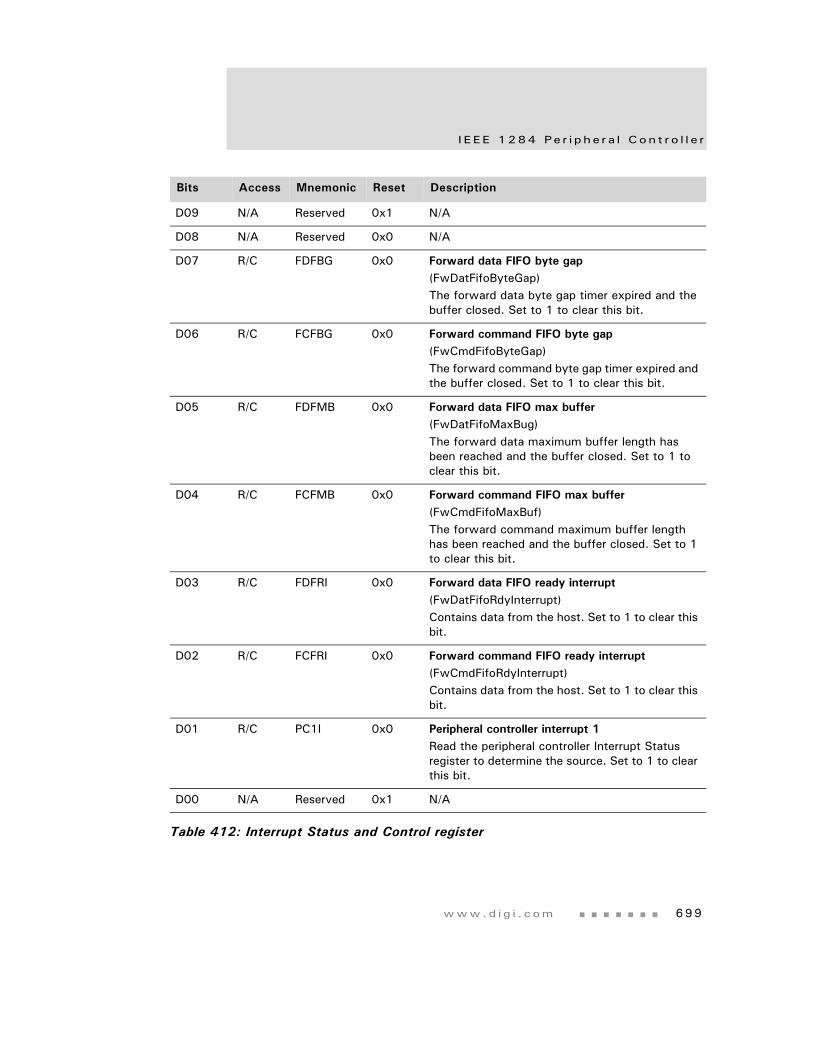
www.d i g i . com 699
I EEE 1284 Pe r i p h e r a l Con t r o l l e r
D09 N/A Reserved 0x1 N/A
D08 N/A Reserved 0x0 N/A
D07 R/C FDFBG 0x0 Forward data FIFO byte gap(FwDatFifoByteGap)The forward data byte gap timer expired and the buffer closed. Set to 1 to clear this bit.
D06 R/C FCFBG 0x0 Forward command FIFO byte gap(FwCmdFifoByteGap)The forward command byte gap timer expired and the buffer closed. Set to 1 to clear this bit.
D05 R/C FDFMB 0x0 Forward data FIFO max buffer(FwDatFifoMaxBug)The forward data maximum buffer length has been reached and the buffer closed. Set to 1 to clear this bit.
D04 R/C FCFMB 0x0 Forward command FIFO max buffer(FwCmdFifoMaxBuf)The forward command maximum buffer length has been reached and the buffer closed. Set to 1 to clear this bit.
D03 R/C FDFRI 0x0 Forward data FIFO ready interrupt(FwDatFifoRdyInterrupt)Contains data from the host. Set to 1 to clear this bit.
D02 R/C FCFRI 0x0 Forward command FIFO ready interrupt(FwCmdFifoRdyInterrupt)Contains data from the host. Set to 1 to clear this bit.
D01 R/C PC1I 0x0 Peripheral controller interrupt 1Read the peripheral controller Interrupt Status register to determine the source. Set to 1 to clear this bit.
D00 N/A Reserved 0x1 N/A
Bits Access Mnemonic Reset Description
Table 412: Interrupt Status and Control register
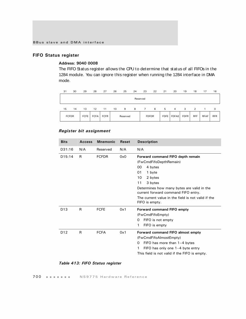
BBus s l a v e a nd DMA i n t e r f a ce
7 0 0 NS9775 Ha r dwa r e Re f e r ence
FIFO Status register
Address: 9040 0008The FIFO Status register allows the CPU to determine that status of all FIFOs in the 1284 module. You can ignore this register when running the 1284 interface in DMA mode.
Register bit assignment
Bits Access Mnemonic Reset Description
D31:16 N/A Reserved N/A N/A
D15:14 R FCFDR 0x0 Forward command FIFO depth remain(FwCmdFifoDepthRemain)00 4 bytes01 1 byte10 2 bytes11 3 bytesDetermines how many bytes are valid in the current forward command FIFO entry. The current value in the field is not valid if the FIFO is empty.
D13 R FCFE 0x1 Forward command FIFO empty(FwCmdFifoEmpty)0 FIFO is not empty1 FIFO is empty
D12 R FCFA 0x1 Forward command FIFO almost empty(FwCmdFifoAlmostEmpty)0 FIFO has more than 1–4 bytes1 FIFO has only one 1–4 byte entryThis field is not valid if the FIFO is empty.
Table 413: FIFO Status register
FCFE FCFA FCFR FDFDR FDFE FDFAE FDFR RFF RFAF
13 12 11 10 9 8 7 6 5 4 3 2 1 015 14
FCFDR
31 29 28 27 26 25 24 23 22 21 20 19 18 17 1630
Reserved
Reserved RFR
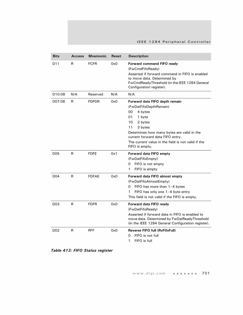
www.d i g i . com 701
I EEE 1284 Pe r i p h e r a l Con t r o l l e r
D11 R FCFR 0x0 Forward command FIFO ready(FwCmdFifoReady)Asserted if forward command in FIFO is enabled to move data. Determined by FwCmdReadyThreshold (in the IEEE 1284 General Configuration register).
D10:08 N/A Reserved N/A N/A
D07:06 R FDFDR 0x0 Forward data FIFO depth remain(FwDatFifoDepthRemain)00 4 bytes01 1 byte10 2 bytes11 3 bytesDetermines how many bytes are valid in the current forward data FIFO entry. The current value in the field is not valid if the FIFO is empty.
D05 R FDFE 0x1 Forward data FIFO empty(FwDatFifoEmpty)0 FIFO is not empty1 FIFO is empty
D04 R FDFAE 0x0 Forward data FIFO almost empty(FwDatFifoAlmostEmpty)0 FIFO has more than 1–4 bytes1 FIFO has only one 1–4 byte entryThis field is not valid if the FIFO is empty.
D03 R FDFR 0x0 Forward data FIFO ready(FwDatFifoReady)Asserted if forward data in FIFO is enabled to move data. Determined by FwDatReadyThreshold (in the IEEE 1284 General Configuration register).
D02 R RFF 0x0 Reverse FIFO full (RvFifoFull)0 FIFO is not full1 FIFO is full
Bits Access Mnemonic Reset Description
Table 413: FIFO Status register
BBus s l a v e a nd DMA i n t e r f a ce
7 0 2 NS9775 Ha r dwa r e Re f e r ence
Forward Command FIFO Read register
Address: 9040 000C
Register bit assignment
D01 R RFAF 0x0 Reverse FIFO almost full (RvFifoAlmostFull)0 FIFO can take more than 1–4 bytes1 FIFO can take only one 1–4 byte entryThis field is not valid id the FIFO is full.
D00 R RFR 0x0 Reverse FIFO ready (RvFifoReady)Asserted if reverse data out FIFO is enabled to move data. Determined by RvDatReadyThreshold (in the IEEE 1284 General Configuration register).
Bits Access Mnemonic Reset Description
Table 413: FIFO Status register
Bits Access Mnemonic Reset Description
D31:00 R FwCmdFifoReadReg N/A Reads up to four bytes from the Forward Command FIFO when in CPU mode. The CPU must read the FIFO Status register (see page 700) to determine how many bytes are remaining before issuing the read.
Table 414: Forward Command FIFO Read register
13 12 11 10 9 8 7 6 5 4 3 2 1 015 14
31 29 28 27 26 25 24 23 22 21 20 19 18 17 1630
FwCmdFifoReadReg
FwCmdFifoReadReg
www.d i g i . com 703
I EEE 1284 Pe r i p h e r a l Con t r o l l e r
Forward Data FIFO Read register
Address: 9040 0010
Register bit assignment
Reverse FIFO Write register/Reverse FIFO Write Register — Last
Address: 9040 001C / 9040 0020Both registers are 32 bits.
Bits Access Mnemonic Reset Description
D31:00 R FwDatFifoReadReg N/A Reads up to four bytes from the Forward Data FIFO when in CPU mode. The CPU must read the FIFO Status register (see page 700) to determine how many bytes are remaining before issuing the read.
Table 415: Forward Data FIFO Read register
13 12 11 10 9 8 7 6 5 4 3 2 1 015 14
31 29 28 27 26 25 24 23 22 21 20 19 18 17 1630
FwDatFifoReadReg
FwDatFifoReadReg
13 12 11 10 9 8 7 6 5 4 3 2 1 015 14
31 29 28 27 26 25 24 23 22 21 20 19 18 17 1630
RvFifoWriteReg
RvFifoWriteReg
BBus s l a v e a nd DMA i n t e r f a ce
7 0 4 NS9775 Ha r dwa r e Re f e r ence
Register bit assignment
Bits Access Mnemonic Reset Description
D31:00 W RvFifoWriteReg N/A Write one to four bytes to the Reverse FIFO when in CPU mode.
A FIFO entry containing one byte or two bytes is written to Reverse FIFO Write Register — Last.
A FIFO entry containing three bytes is written in two steps:
Step 1: The lowest 16 bits are written to the Reverse FIFO Register.
Step 2: The high byte is written to the Reverse FIFO Write Register — Last.
A FIFO entry containing four bytes is written to either register.
D31:00 W RvFifoWriteReg — Last
N/A
Table 416: Reverse Data FIFO Write register/Reverse Data FIFO Write Register — Last
13 12 11 10 9 8 7 6 5 4 3 2 1 015 14
31 29 28 27 26 25 24 23 22 21 20 19 18 17 1630
RvFifoWriteReg - Last
RvFifoWriteReg - Last
www.d i g i . com 705
I EEE 1284 Pe r i p h e r a l Con t r o l l e r
Forward Command DMA Control register
Address: 9040 0024The Forward Command DMA Control register controls when the Forward command DMA buffer is closed, using two components:
16-bit maximum buffer counter. The maximum buffer counter increments each time a DMA transfer occurs, by the number of bytes in the transfer. The counter is reset each time a DMA is completed. If the counter reaches or exceeds the forward command maximum buffer size (FwCmdMaxBufSize), the 1284 module signals the DMA channel to close the buffer and start a new one. A (maskable) interrupt is generated when FwCmdMaxBufSize is reached. Future bytes are moved using DMA when the next DMA is initiated by the DMA controller.
Note: This counter should not be set to a value greater than the buffer length field value set in the 1284 forward command channel descriptor.
16-bit byte gap counter. The byte gap counter increments on each clock cycle when a byte is not read from the host, with a maximum programmable interval of 1.3 ms based on a 50 MHz BBus clock. The counter is reset when a byte is read from the host. If the counter reaches the forward command byte gap timeout (FwCmdByteGapTimer), the following occurs:
a Where the FIFOs are written with dwords containing four bytes each, the gap timeout forces an incomplete dword (that is, 1–3 bytes) to be written to the FIFO.
b Forward command FIFO ready, which usually means the threshold has been met, is asserted. This results in continuation of the currently active DMA until the FIFO is empty.
c When the data in the FIFO, including the incomplete dwords in Step 1, is output through DMA, the DMA is terminated.
13 12 11 10 9 8 7 6 5 4 3 2 1 015 14
31 29 28 27 26 25 24 23 22 21 20 19 18 17 1630
FwCmdMaxBufSize
FwCmdByteGapTimer
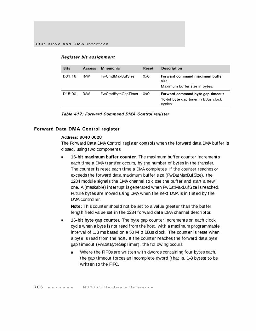
BBus s l a v e a nd DMA i n t e r f a ce
7 0 6 NS9775 Ha r dwa r e Re f e r ence
Register bit assignment
Forward Data DMA Control register
Address: 9040 0028The Forward Data DMA Control register controls when the forward data DMA buffer is closed, using two components:
16-bit maximum buffer counter. The maximum buffer counter increments each time a DMA transfer occurs, by the number of bytes in the transfer. The counter is reset each time a DMA completes. If the counter reaches or exceeds the forward data maximum buffer size (FwDatMaxBufSize), the 1284 module signals the DMA channel to close the buffer and start a new one. A (maskable) interrupt is generated when FwDatMaxBufSize is reached. Future bytes are moved using DMA when the next DMA is initiated by the DMA controller.
Note: This counter should not be set to a value greater than the buffer length field value set in the 1284 forward data DMA channel descriptor.
16-bit byte gap counter. The byte gap counter increments on each clock cycle when a byte is not read from the host, with a maximum programmable interval of 1.3 ms based on a 50 MHz BBus clock. The counter is reset when a byte is read from the host. If the counter reaches the forward data byte gap timeout (FwDatByteGapTimer), the following occurs:
a Where the FIFOs are written with dwords containing four bytes each, the gap timeout forces an incomplete dword (that is, 1–3 bytes) to be written to the FIFO.
Bits Access Mnemonic Reset Description
D31:16 R/W FwCmdMaxBufSize 0x0 Forward command maximum buffer sizeMaximum buffer size in bytes.
D15:00 R/W FwCmdByteGapTimer 0x0 Forward command byte gap timeout16-bit byte gap timer in BBus clock cycles.
Table 417: Forward Command DMA Control register
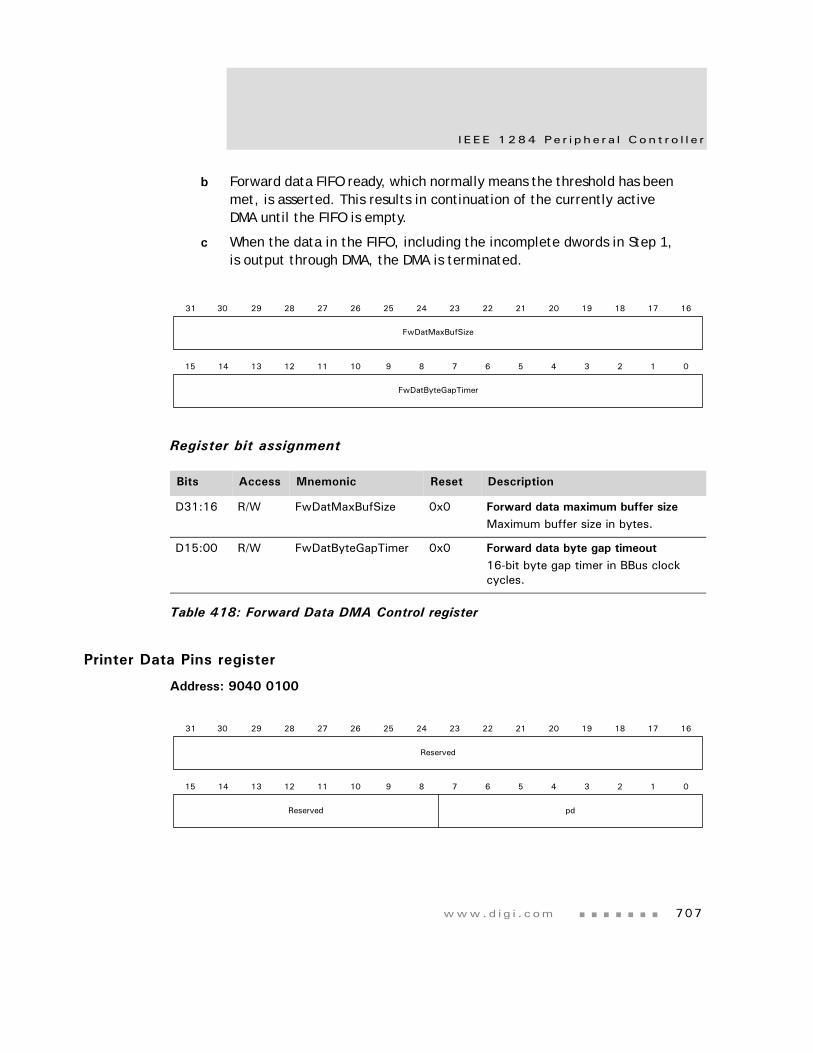
www.d i g i . com 707
I EEE 1284 Pe r i p h e r a l Con t r o l l e r
b Forward data FIFO ready, which normally means the threshold has been met, is asserted. This results in continuation of the currently active DMA until the FIFO is empty.
c When the data in the FIFO, including the incomplete dwords in Step 1, is output through DMA, the DMA is terminated.
Register bit assignment
Printer Data Pins register
Address: 9040 0100
Bits Access Mnemonic Reset Description
D31:16 R/W FwDatMaxBufSize 0x0 Forward data maximum buffer sizeMaximum buffer size in bytes.
D15:00 R/W FwDatByteGapTimer 0x0 Forward data byte gap timeout16-bit byte gap timer in BBus clock cycles.
Table 418: Forward Data DMA Control register
13 12 11 10 9 8 7 6 5 4 3 2 1 015 14
31 29 28 27 26 25 24 23 22 21 20 19 18 17 1630
FwDatMaxBufSize
FwDatByteGapTimer
pd
13 12 11 10 9 8 7 6 5 4 3 2 1 015 14
31 29 28 27 26 25 24 23 22 21 20 19 18 17 1630
Reserved
Reserved
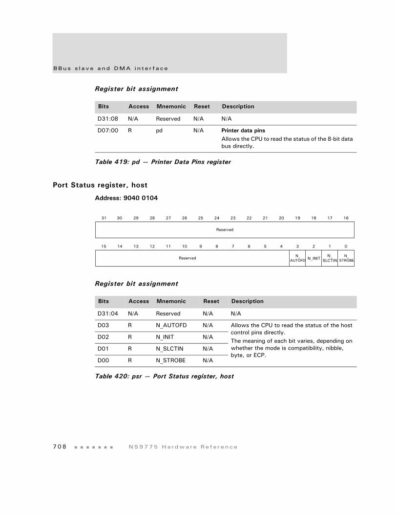
BBus s l a v e a nd DMA i n t e r f a ce
7 0 8 NS9775 Ha r dwa r e Re f e r ence
Register bit assignment
Port Status register, host
Address: 9040 0104
Register bit assignment
Bits Access Mnemonic Reset Description
D31:08 N/A Reserved N/A N/A
D07:00 R pd N/A Printer data pinsAllows the CPU to read the status of the 8-bit data bus directly.
Table 419: pd — Printer Data Pins register
Bits Access Mnemonic Reset Description
D31:04 N/A Reserved N/A N/A
D03 R N_AUTOFD N/A Allows the CPU to read the status of the host control pins directly.The meaning of each bit varies, depending on whether the mode is compatibility, nibble, byte, or ECP.
D02 R N_INIT N/A
D01 R N_SLCTIN N/A
D00 R N_STROBE N/A
Table 420: psr — Port Status register, host
13 12 11 10 9 8 7 6 5 4 3 2 1 015 14
31 29 28 27 26 25 24 23 22 21 20 19 18 17 1630
Reserved
Reserved N_AUTOFD N_INIT
N_SLCTIN
N_STROBE
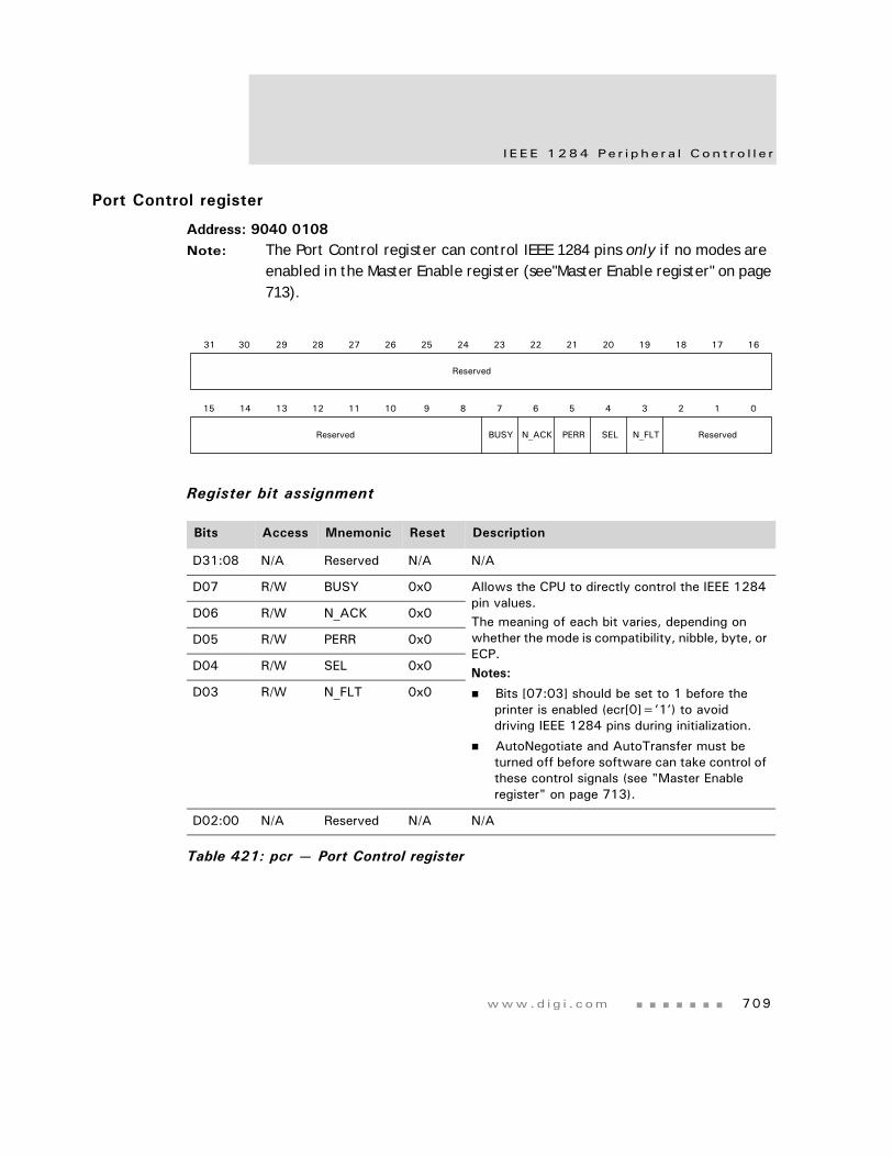
www.d i g i . com 709
I EEE 1284 Pe r i p h e r a l Con t r o l l e r
Port Control register
Address: 9040 0108Note: The Port Control register can control IEEE 1284 pins only if no modes are
enabled in the Master Enable register (see"Master Enable register" on page 713).
Register bit assignment
Bits Access Mnemonic Reset Description
D31:08 N/A Reserved N/A N/A
D07 R/W BUSY 0x0 Allows the CPU to directly control the IEEE 1284 pin values.The meaning of each bit varies, depending on whether the mode is compatibility, nibble, byte, or ECP.Notes:
Bits [07:03] should be set to 1 before the printer is enabled (ecr[0]=’1’) to avoid driving IEEE 1284 pins during initialization.
AutoNegotiate and AutoTransfer must be turned off before software can take control of these control signals (see "Master Enable register" on page 713).
D06 R/W N_ACK 0x0
D05 R/W PERR 0x0
D04 R/W SEL 0x0
D03 R/W N_FLT 0x0
D02:00 N/A Reserved N/A N/A
Table 421: pcr — Port Control register
BUSY N_ACK PERR SEL N_FLT
13 12 11 10 9 8 7 6 5 4 3 2 1 015 14
31 29 28 27 26 25 24 23 22 21 20 19 18 17 1630
Reserved
Reserved Reserved
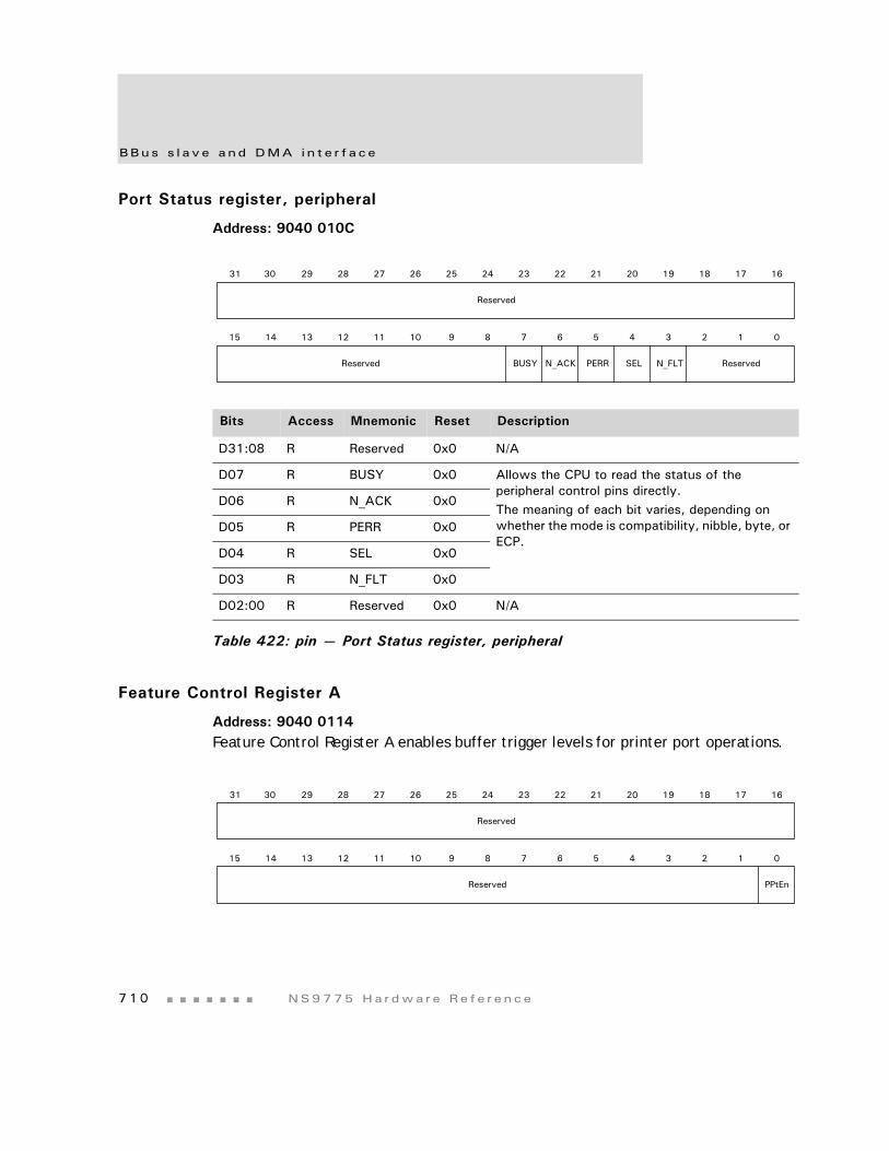
BBus s l a v e a nd DMA i n t e r f a ce
7 1 0 NS9775 Ha r dwa r e Re f e r ence
Port Status register, peripheral
Address: 9040 010C
Feature Control Register A
Address: 9040 0114Feature Control Register A enables buffer trigger levels for printer port operations.
Bits Access Mnemonic Reset Description
D31:08 R Reserved 0x0 N/A
D07 R BUSY 0x0 Allows the CPU to read the status of the peripheral control pins directly. The meaning of each bit varies, depending on whether the mode is compatibility, nibble, byte, or ECP.
D06 R N_ACK 0x0
D05 R PERR 0x0
D04 R SEL 0x0
D03 R N_FLT 0x0
D02:00 R Reserved 0x0 N/A
Table 422: pin — Port Status register, peripheral
BUSY N_ACK PERR SEL N_FLT
13 12 11 10 9 8 7 6 5 4 3 2 1 015 14
31 29 28 27 26 25 24 23 22 21 20 19 18 17 1630
Reserved
Reserved Reserved
13 12 11 10 9 8 7 6 5 4 3 2 1 015 14
31 29 28 27 26 25 24 23 22 21 20 19 18 17 1630
Reserved
Reserved PPtEn
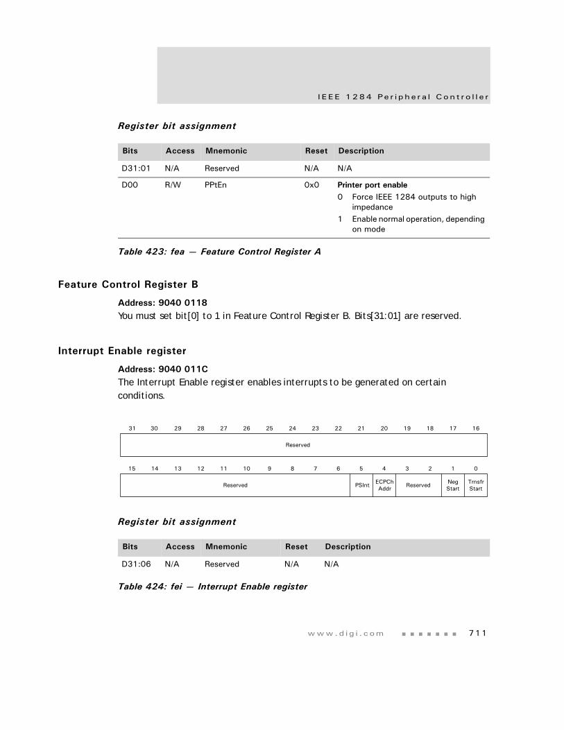
www.d i g i . com 711
I EEE 1284 Pe r i p h e r a l Con t r o l l e r
Register bit assignment
Feature Control Register B
Address: 9040 0118You must set bit[0] to 1 in Feature Control Register B. Bits[31:01] are reserved.
Interrupt Enable register
Address: 9040 011CThe Interrupt Enable register enables interrupts to be generated on certain conditions.
Register bit assignment
Bits Access Mnemonic Reset Description
D31:01 N/A Reserved N/A N/A
D00 R/W PPtEn 0x0 Printer port enable0 Force IEEE 1284 outputs to high
impedance1 Enable normal operation, depending
on mode
Table 423: fea — Feature Control Register A
Bits Access Mnemonic Reset Description
D31:06 N/A Reserved N/A N/A
Table 424: fei — Interrupt Enable register
PSInt
13 12 11 10 9 8 7 6 5 4 3 2 1 015 14
31 29 28 27 26 25 24 23 22 21 20 19 18 17 1630
Reserved
Reserved NegStart
TrnsfrStart
ECPChAddr Reserved
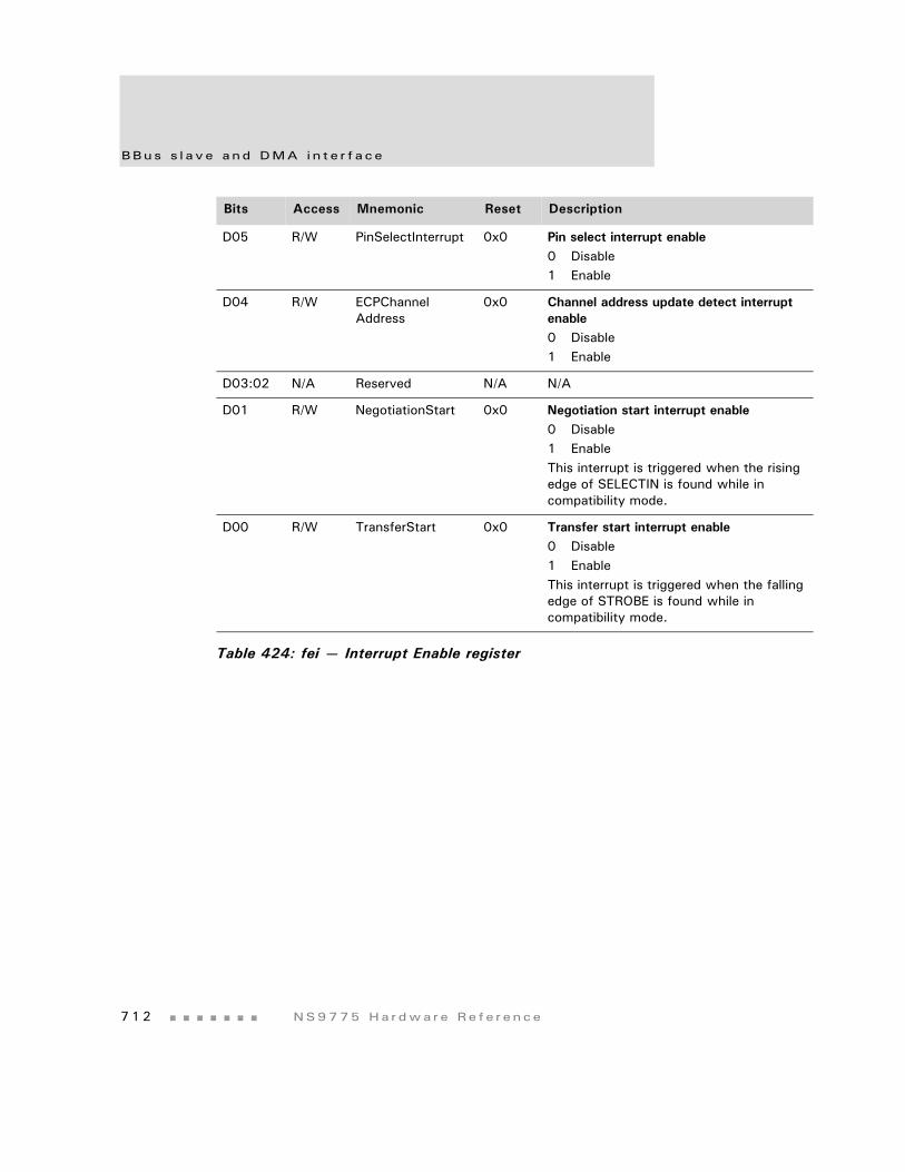
BBus s l a v e a nd DMA i n t e r f a ce
7 1 2 NS9775 Ha r dwa r e Re f e r ence
D05 R/W PinSelectInterrupt 0x0 Pin select interrupt enable0 Disable1 Enable
D04 R/W ECPChannelAddress
0x0 Channel address update detect interrupt enable0 Disable1 Enable
D03:02 N/A Reserved N/A N/A
D01 R/W NegotiationStart 0x0 Negotiation start interrupt enable0 Disable1 EnableThis interrupt is triggered when the rising edge of SELECTIN is found while in compatibility mode.
D00 R/W TransferStart 0x0 Transfer start interrupt enable0 Disable1 EnableThis interrupt is triggered when the falling edge of STROBE is found while in compatibility mode.
Bits Access Mnemonic Reset Description
Table 424: fei — Interrupt Enable register
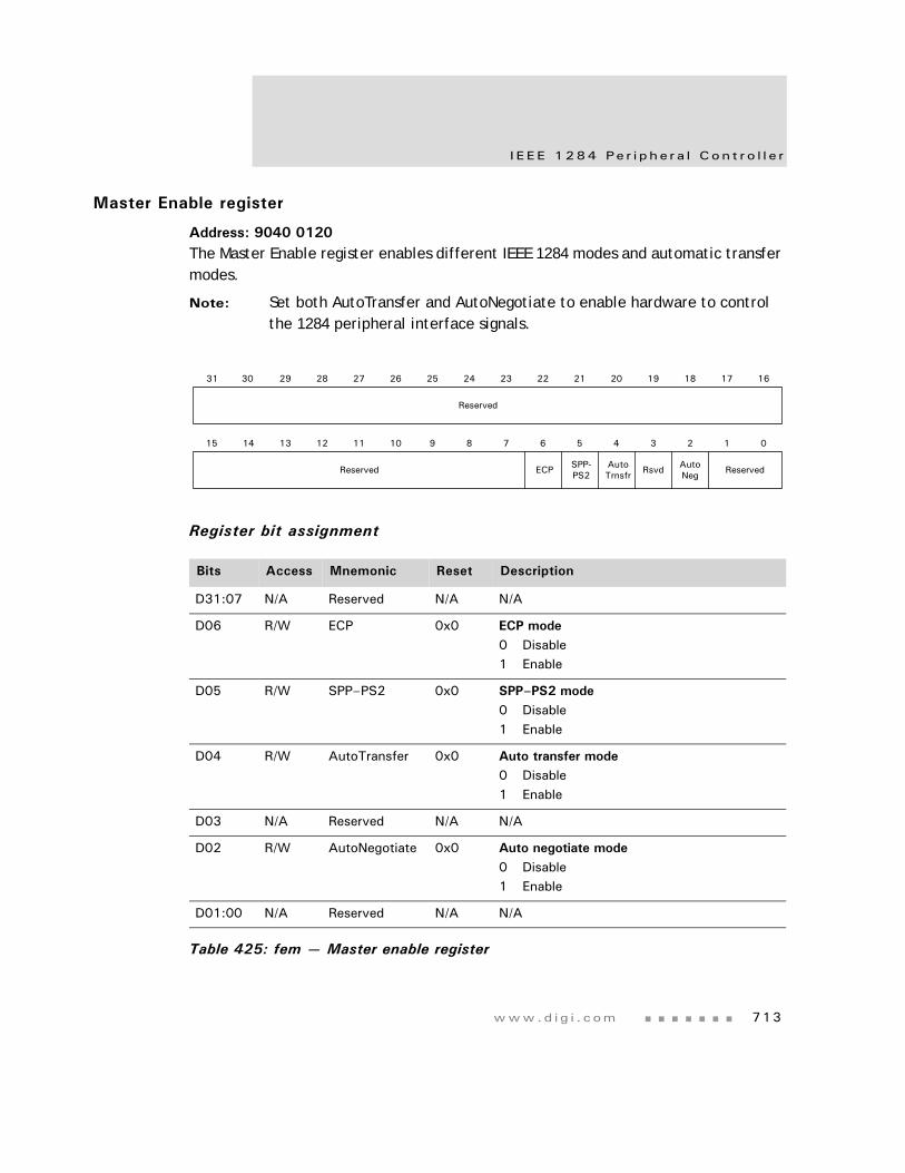
www.d i g i . com 713
I EEE 1284 Pe r i p h e r a l Con t r o l l e r
Master Enable register
Address: 9040 0120The Master Enable register enables different IEEE 1284 modes and automatic transfer modes.
Note: Set both AutoTransfer and AutoNegotiate to enable hardware to control the 1284 peripheral interface signals.
Register bit assignment
Bits Access Mnemonic Reset Description
D31:07 N/A Reserved N/A N/A
D06 R/W ECP 0x0 ECP mode0 Disable1 Enable
D05 R/W SPP–PS2 0x0 SPP–PS2 mode0 Disable1 Enable
D04 R/W AutoTransfer 0x0 Auto transfer mode0 Disable1 Enable
D03 N/A Reserved N/A N/A
D02 R/W AutoNegotiate 0x0 Auto negotiate mode0 Disable1 Enable
D01:00 N/A Reserved N/A N/A
Table 425: fem — Master enable register
ECP SPP-PS2
AutoTrnsfr
13 12 11 10 9 8 7 6 5 4 3 2 1 015 14
31 29 28 27 26 25 24 23 22 21 20 19 18 17 1630
Reserved
Reserved Rsvd AutoNeg Reserved
BBus s l a v e a nd DMA i n t e r f a ce
7 1 4 NS9775 Ha r dwa r e Re f e r ence
Extensibility Byte Requested by Host
Address: 9040 0124This register is updated shortly after a new negotiation occurs (event 4 of the negotiation process; see the IEEE 1284 standard for more information).
Register bit assignment
Extended Control register
Address: 9040 0128The Extended Control register enables additional core features.
Bits Access Mnemonic Reset Description
D31:08 N/A Reserved N/A N/A
D07:00 R/W exr 0x0 Extensibility byteStores the extensibility byte received from the host.
Table 426: exr — Extensibility Byte Requested by Host register
exr
13 12 11 10 9 8 7 6 5 4 3 2 1 015 14
31 29 28 27 26 25 24 23 22 21 20 19 18 17 1630
Reserved
Reserved
Notused
EnRevDtTrn
13 12 11 10 9 8 7 6 5 4 3 2 1 015 14
31 29 28 27 26 25 24 23 22 21 20 19 18 17 1630
Reserved
Reserved Reserved
www.d i g i . com 715
I EEE 1284 Pe r i p h e r a l Con t r o l l e r
Register bit assignment
Interrupt Status register
Address: 9040 012CInterrupts are cleared when this register is read. These interrupts are needed by software no matter which mode (DMA or CPU) is being used.
Register bit assignment
Bits Access Mnemonic Reset Description
D31:08 N/A Reserved N/A N/A
D07 N/A Not used 0x0 Set to 1.
D06 R/W Enable reverse data transfers 0x0 0 Disable1 Enable
D05:00 N/A Reserved N/A N/A
Table 427: ecr — Extended Control register
Bits Access Mnemonic Reset Description
D31:06 N/A Reserved N/A N/A
D05 R PSINT 0x0 Pin select interrupt
D04 R ECP Channel Address
0x0 Channel address update detect interrupt
D03:02 N/A Reserved N/A N/A
D01 R NSDI 0x0 Negotiation start detect interrupt
Table 428: sti — Interrupt Status register
PSINT
13 12 11 10 9 8 7 6 5 4 3 2 1 015 14
31 29 28 27 26 25 24 23 22 21 20 19 18 17 1630
Reserved
Reserved NSDIECPChAddr TSDIReserved
BBus s l a v e a nd DMA i n t e r f a ce
7 1 6 NS9775 Ha r dwa r e Re f e r ence
Pin Interrupt Mask register
Address: 9040 0134The Pin Interrupt Mask register enables IEEE 1284 pin interrupts.
D00 R TSDI 0x0 Transfer start detect interrupt
Bits Access Mnemonic Reset Description
Table 428: sti — Interrupt Status register
Bits Access Mnemonic Reset Description
D31:04 N/A Reserved 0x0 N/A
D03 R/W n_autofd edge detect 0x0 0 Disable1 EnableD02 R/W n_init edge detect 0x0
D01 R/W n_selectin edge detect 0x0
D00 R/W n_strobe edge detect 0x0
Table 429: msk — Pin Interrupt Mask register
13 12 11 10 9 8 7 6 5 4 3 2 1 015 14
31 29 28 27 26 25 24 23 22 21 20 19 18 17 1630
Reserved
ReservedN_
AUTOFDedge det
N_INITedge
detect
N_SLCTINedge det
N_STROBEedge det
www.d i g i . com 717
I EEE 1284 Pe r i p h e r a l Con t r o l l e r
Pin Interrupt Control register
Address: 9040 0138The Pin Interrupt Control register configures IEEE 1284 pin interrupt edge levels.
Register bit assignment
Bits Access Mnemonic Reset Description
D31:04 R Reserved 0x0 N/A
D03 R/W n_autofd edge 0x0 0 Falling edge1 Rising edgeD02 R/W n_init edge 0x0
D01 R/W n_slctin edge 0x0
D00 R/W n_strobe edge 0x0
Table 430: pit — Pin Interrupt Control register
n_autofdedge
n_initedge
n_slctinedge
n_strobeedge
13 12 11 10 9 8 7 6 5 4 3 2 1 015 14
31 29 28 27 26 25 24 23 22 21 20 19 18 17 1630
Reserved
Reserved
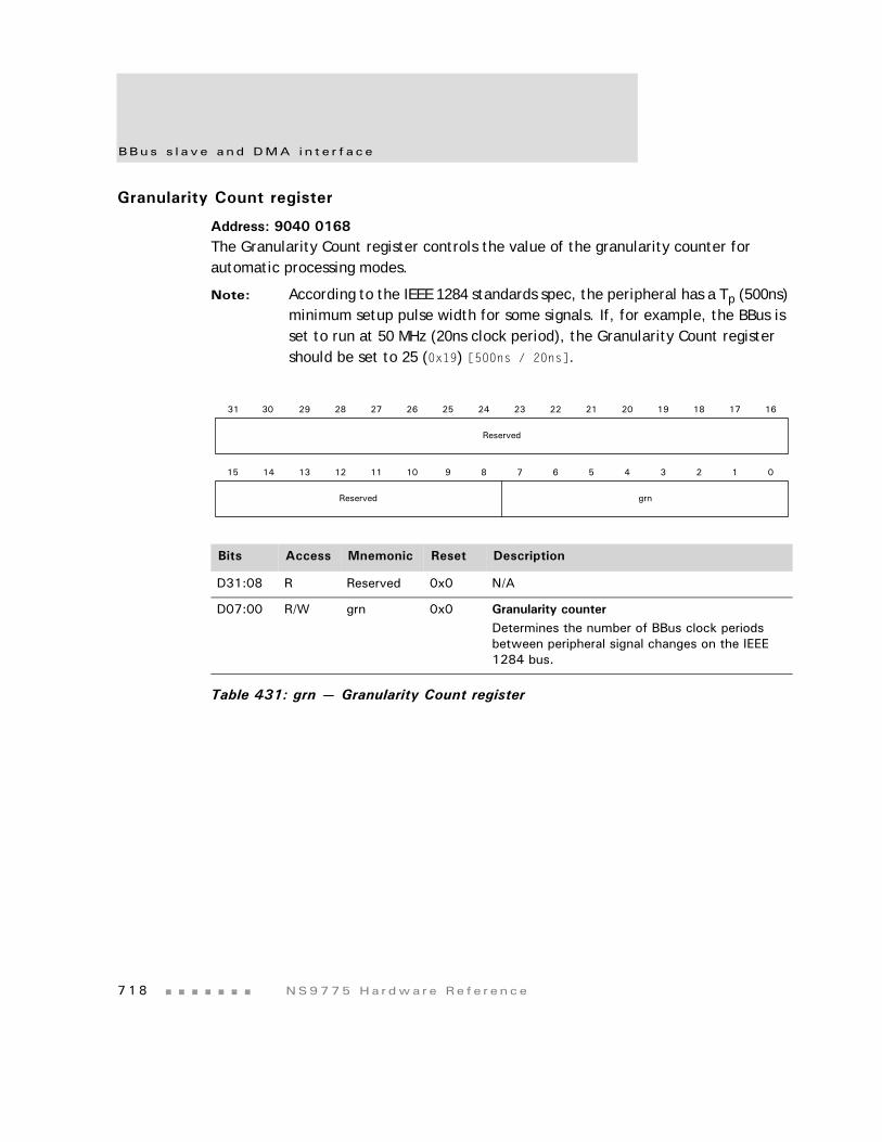
BBus s l a v e a nd DMA i n t e r f a ce
7 1 8 NS9775 Ha r dwa r e Re f e r ence
Granularity Count register
Address: 9040 0168The Granularity Count register controls the value of the granularity counter for automatic processing modes.
Note: According to the IEEE 1284 standards spec, the peripheral has a Tp (500ns) minimum setup pulse width for some signals. If, for example, the BBus is set to run at 50 MHz (20ns clock period), the Granularity Count register should be set to 25 (0x19) [500ns / 20ns].
Bits Access Mnemonic Reset Description
D31:08 R Reserved 0x0 N/A
D07:00 R/W grn 0x0 Granularity counterDetermines the number of BBus clock periods between peripheral signal changes on the IEEE 1284 bus.
Table 431: grn — Granularity Count register
grn
13 12 11 10 9 8 7 6 5 4 3 2 1 015 14
31 29 28 27 26 25 24 23 22 21 20 19 18 17 1630
Reserved
Reserved
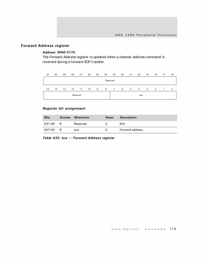
www.d i g i . com 719
I EEE 1284 Pe r i p h e r a l Con t r o l l e r
Forward Address register
Address: 9040 0174The Forward Address register is updated when a channel address command is received during a forward ECP transfer.
Register bit assignment
Bits Access Mnemonic Reset Description
D31:08 R Reserved 0 N/A
D07:00 R eca 0 Forward address.
Table 432: eca — Forward Address register
eca
13 12 11 10 9 8 7 6 5 4 3 2 1 015 14
31 29 28 27 26 25 24 23 22 21 20 19 18 17 1630
Reserved
Reserved
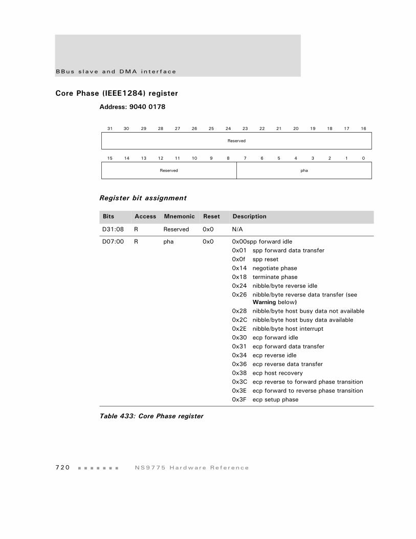
BBus s l a v e a nd DMA i n t e r f a ce
7 2 0 NS9775 Ha r dwa r e Re f e r ence
Core Phase (IEEE1284) register
Address: 9040 0178
Register bit assignment
Bits Access Mnemonic Reset Description
D31:08 R Reserved 0x0 N/A
D07:00 R pha 0x0 0x00spp forward idle0x01 spp forward data transfer0x0f spp reset0x14 negotiate phase0x18 terminate phase0x24 nibble/byte reverse idle0x26 nibble/byte reverse data transfer (see
Warning below)0x28 nibble/byte host busy data not available0x2C nibble/byte host busy data available0x2E nibble/byte host interrupt0x30 ecp forward idle0x31 ecp forward data transfer0x34 ecp reverse idle0x36 ecp reverse data transfer0x38 ecp host recovery0x3C ecp reverse to forward phase transition0x3E ecp forward to reverse phase transition0x3F ecp setup phase
Table 433: Core Phase register
pha
13 12 11 10 9 8 7 6 5 4 3 2 1 015 14
31 29 28 27 26 25 24 23 22 21 20 19 18 17 1630
Reserved
Reserved
www.d i g i . com 721
I EEE 1284 Pe r i p h e r a l Con t r o l l e r
Warning: The NS9775 cannot proceed to the Host Busy Data Available protocol state directly from negotiation state. If the host software supports the 1284 protocol reverse idle and interrupt host states (events 7, 18 – 20), the impact is a one-time loss of approximately 2,000ns at the beginning of data transfer. If the host does not support these states, however, the NS9775 will be unable to transmit data in nibble or byte mode. Note that there is no impact for a host that fully implements IEEE 1284.

723
USB Controller ModuleC H A P T E R 1 6
USB 2.0 provides a standard “plug-and-play” interface for desktop communications at low to moderate speeds. The USB module in NS9775 supports both full-speed (12Mbps) and low-speed (1.5 Mbps) operation.
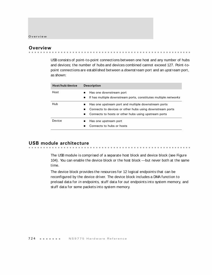
Ove r v i ew
7 2 4 NS9775 Ha r dwa r e Re f e r ence
Overview
USB consists of point-to-point connections between one host and any number of hubs and devices; the number of hubs and devices combined cannot exceed 127. Point-to-point connections are established between a downstream port and an upstream port, as shown:
USB module architecture
The USB module is comprised of a separate host block and device block (see Figure 104). You can enable the device block or the host block — but never both at the same time.
The device block provides the resources for 12 logical endpoints that can be reconfigured by the device driver. The device block includes a DMA function to preload data for in endpoints, stuff data for out endpoints into system memory, and stuff data for some packets into system memory.
Host/hub/device Description
Host Has one downstream port
If has multiple downstream ports, constitutes multiple networks
Hub Has one upstream port and multiple downstream ports
Connects to devices or other hubs using downstream ports
Connects to hosts or other hubs using upstream ports
Device Has one upstream port
Connects to hubs or hosts
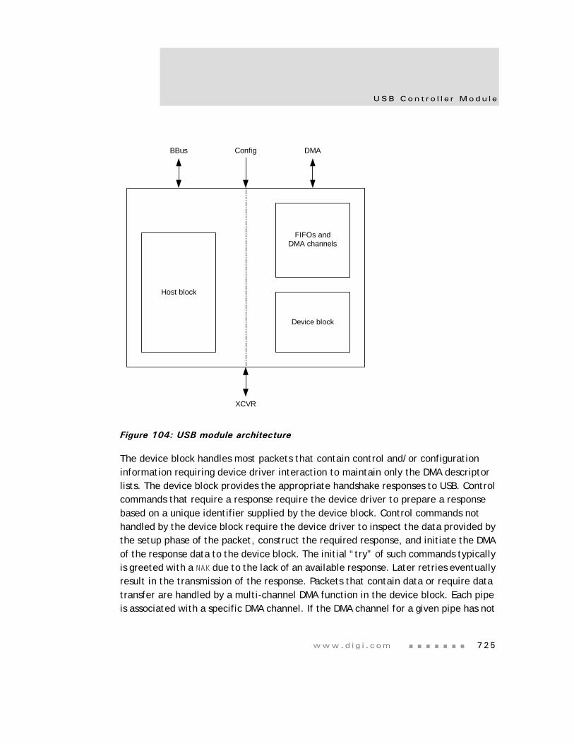
www.d i g i . com 725
USB Con t r o l l e r Modu l e
Figure 104: USB module architecture
The device block handles most packets that contain control and/or configuration information requiring device driver interaction to maintain only the DMA descriptor lists. The device block provides the appropriate handshake responses to USB. Control commands that require a response require the device driver to prepare a response based on a unique identifier supplied by the device block. Control commands not handled by the device block require the device driver to inspect the data provided by the setup phase of the packet, construct the required response, and initiate the DMA of the response data to the device block. The initial “try” of such commands typically is greeted with a NAK due to the lack of an available response. Later retries eventually result in the transmission of the response. Packets that contain data or require data transfer are handled by a multi-channel DMA function in the device block. Each pipe is associated with a specific DMA channel. If the DMA channel for a given pipe has not
FIFOs andDMA channels
Device block
Host block
BBus Config DMA
XCVR
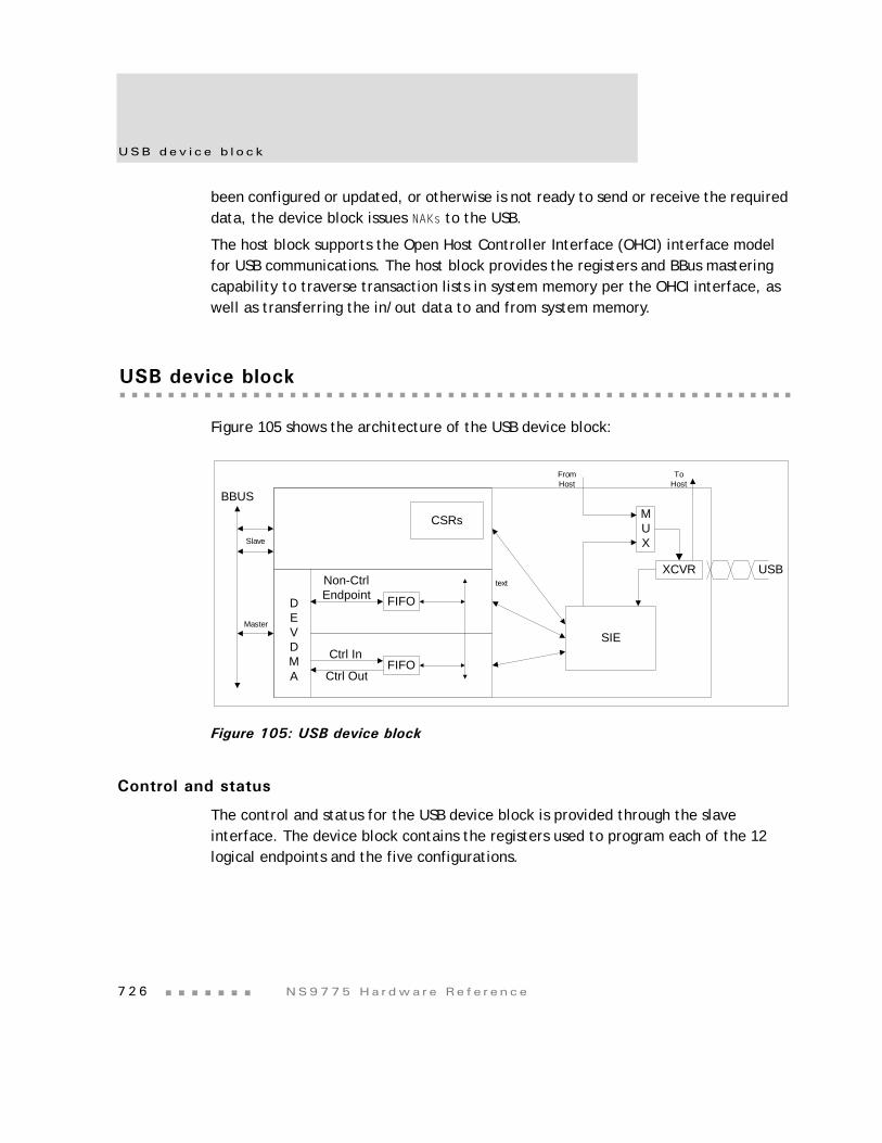
USB dev i c e b l o c k
7 2 6 NS9775 Ha r dwa r e Re f e r ence
been configured or updated, or otherwise is not ready to send or receive the required data, the device block issues NAKs to the USB.
The host block supports the Open Host Controller Interface (OHCI) interface model for USB communications. The host block provides the registers and BBus mastering capability to traverse transaction lists in system memory per the OHCI interface, as well as transferring the in/out data to and from system memory.
USB device block
Figure 105 shows the architecture of the USB device block:
Figure 105: USB device block
Control and status
The control and status for the USB device block is provided through the slave interface. The device block contains the registers used to program each of the 12 logical endpoints and the five configurations.
text
CSRs
DEVDMA
Non-CtrlEndpoint FIFO
FIFOCtrl In
Ctrl Out
SIE
MUX
XCVR
Slave
Master
BBUS
FromHost
ToHost
USB
www.d i g i . com 727
USB Con t r o l l e r Modu l e
Packet and data flow
The device block responds to packets initiated by the host. There are 16 DMA channels in this block. DMA channels 1 and 2 move data to and from system memory for control transfers for logical endpoint 0. DMA channels 3 through 13 move data for logical endpoints 1 through 11, respectively. DMA channels 14 through 16 are not used in the USB module.
Data for each logical endpoint travels through a four-word FIFO. Logic included with the FIFOs interface the Master I/F to the DMA channels. The serial interface engine (SIE) performs the tasks required to receive and send packets to and from a USB host.
The device driver writes the endpoint descriptor, configuration identifier register, string identifiers, DMA parameters, and the direction of data transmission for logical endpoints 1–11. From that point, the device driver monitors packet reception/transmission success, and maintains the DMA descriptor lists. DMA Channel 1 DMA descriptors are incoming; that is, they move data from USB to memory. DMA channel 2 DMA descriptors are outgoing; that is, they move data from memory to the USB. The remainder of the DMA descriptors must follow the direction of data flow for the corresponding logical endpoint, which is also specified in the control/status register for the channel.
When a packet is received, a DMA descriptor must be available to move the required data; otherwise, the packet fails. If a descriptor remains unavailable, the FIFOs will be exhausted and an underrun or overrflow condition occurs. Bits in the corresponding FIFO Status register are set. DMA channels can be used to signal a DMA with no descriptors available.
Control in packets
Control in packets require device driver intervention. An “identifier” is stored in the status field of a retired DMA descriptor doe DMA channel 1. The device driver constructs a response and moves the response from system memory to the USB with DMA channel 2. The USB response to the initial reception of the control in packet is to store the identifier, then NAK the packet; this causes the host to retry the packet. If the outgoing data has been moved to the USB, the data is output upon retry. Once a control in packet has been received, all control in packets are NAK’d, and their identifiers are not stored. The first control in packet received following the successful transmission of data for the previous “pending” packet becomes the new “pending” packet.
Hos t b l o c k
7 2 8 NS9775 Ha r dwa r e Re f e r ence
Logical and physical endpoints
Each alternate of each interface of each configuration can use as many as 16 logical endpoints. Physical endpoints in the device block are programmable by software for configuration/interface/alternate number. type, direction, and MaxPacketSize. A physical endpoint, then, functions as one logical endpoint in one alternate of one interface of one configuration. The number of physical endpoints required is therefore equal to the total number of logical endpoints in each alternate of each interface of each configuration.
The device block is configured to hold 12 physical endpoints, endpoint 0, and 11 non-control endpoints, with a maximum of 5 interfaces. This allows simultaneous operation of the printer class, still image class, and three instances of the data class. Programming of the physical endpoints and the descriptors provided allow you to reassign any of the physical endpoints to any one of the five interfaces. A “multi-function” fax/printer scanner device can take the place of three instances of the data class if no more than six physical endpoints are required.
Slew rates
USB PHY has a greater than specified slew rate in low speed device mode. Faster slew rates may cause compatibility issues with low speed hosts.
Host block
The USB host block contains the resources to implement an OHCI host. These resources include a power control signal for USB port power. Figure 106 shows the architecture for the USB host block.
Control and status
The control and status for the USB host block is provided using the slave interface. The registers support the OHCI specification.
www.d i g i . com 729
USB Con t r o l l e r Modu l e
Figure 106: USB host architecture
Packet data flow
The host block initiates all transfers on the USB. Data travels through a four-word FIFO in either direction. The Serial Interface Engine (SIE) performs the tasks required to receive and send packets on the USB.
The host block is the master of the USB. At the highest level, the host maintains a database of the existing network topology, and can reconfigure any associated device.
At the next level, there are four linked lists of endpoint descriptors, each tied to one or more transfer descriptors. The four lists correspond to the four endpoint types that are accessed in a specified priority. The host begins processing these lists each millisecond, after sending the SOF packet. When a given endpoint descriptor is processed, the host generates a packet to move data and the transfer descriptor(s) defines the source or destination of the data in system memory. Interrupts generally are generated as each transfer descriptor is retired.
The core is connected with a master interface on the BBus to move incoming or outgoing data to system memory. Based on expected timing of four microseconds for bus turnaround, the four-word FIFOs included in the core prevent underrun and/or overrun occurrences. Bursting is supported to minimize the bus bandwidth that is
text
OHCIRegs
FIFO
FIFO
BBUS
Slave IF
Master IF
SIE
To XCVR From XCVR
USB dev i c e e ndpo i n t
7 3 0 NS9775 Ha r dwa r e Re f e r ence
consumed. Burst transfers move a maximum of 8 bytes in long word transactions. FIFO content from more than one transfer descriptor is broken into separate memory operations.
USB device endpoint
Any USB device requires a bidirectional control endpoint located at endpoint #0. The data FIFOs in the USB device application logic are unidirectional, so two data FIFOs are used to create a single bidirectional endpoint. FIFO #1 handles the USB-OUT packets and FIFO #2 handles the USB-IN packets. Table 434 describes the fields in the FIFO Status and Control registers that must be set in order for the bidirectional control endpoint to operate. The remaining Control register fields are application-specific.
Transmission error handling
USB protocol supports the error-free transmission of packets for bulk and interrupt endpoints. The USB device application logic contains some control structures to help the software with this task. Transmission errors are defined as bit-stuffing errors or CRC check errors.
FIFO Mnemonic Value Description
1 TYPE 00 Control endpoint
1 DIR 0 USB-OUT direction
2 TYPE 00 Control endpoint
2 DIR 1 USB-IN direction
Table 434: Control endpoint register requirements
www.d i g i . com 731
USB Con t r o l l e r Modu l e
Handling USB-IN packet errors
USB-IN packet errors are sent from the USB device to the USB host. The USB host either responds with an ACK packet to indicate successful transmission or does not respond at all to indicate that there was an error in transmission.
These are the steps that must be taken to retransmit the packet in error:
1 Determine that the error has occurred through an interrupt. The hardware places the endpoint FIFO into reset state and flushes the contents.
2 Determine which endpoint is involved, using the FIFO Status registers.
3 Read the valid packets-transmitted-count from the Packet Control register and use it to compute a new buffer descriptor source address and buffer length. Update the current buffer descriptor in system memory. The current DMA buffer descriptor can be determined by reading the index field in the DMA Control register (see "DMA Control register" on page 526).
4 Write a 1 to the BDR (buffer descriptor refetch) and CE (channel enable) fields in the DMA Control register to force a refetch of the buffer descriptor when the channel next wins arbitration.
5 Take the USB device endpoint FIFO out of reset. At this point, the DMA controller will refetch the buffer descriptor as well as the packet in error and all remaining data in the DMA buffer.
Handling USB-OUT packet errors
USB-OUT packets are sent from the USB host to the USB device. The USB device either responds with an ACK packet to indicate successful transmission or does not respond at all to indicate that there was an error in transmission. If there was an error, the current DMA buffer is closed and the DMA buffer descriptor status field indicates that an error has occurred. Through this status information, software knows to discard the last packet in the buffer, as the USB host will retransmit the packet in error. The DMA controller fetches the next buffer descriptor, and the retransmitted packet will be the first packet in the new DMA data buffer.
USB b l o ck r e g i s t e r s
7 3 2 NS9775 Ha r dwa r e Re f e r ence
USB block registers
The USB module configuration registers are located at base address 9010_0000. Table 435 provides the address register map for the USB “modules” within the USB block.
USB Global registers
Table 436 provides the addresses for the USB Global registers.
All configuration registers must be accessed as 32-bit words and as single accesses only. No bursting is allowed.
Address range Register space (module)
0x90100000–0x90100FFF USB Global Control and Status
0x90101000–0x90101FFF USB Host Block
0x90102000–0x90102FFF USB Device Block
0x90103000–0x90103FFF USB Device Endpoint FIFOs
0x90110000–0x9011FFFF USB Device DMA (see the BBus DMA Controller chapter for details about these registers)
Table 435: USB register address map
Address Register
9010 0000 Global Control/Status register
9010 0004 Device Control/Status register
9010 000C Global Interrupt Enable
9010 0010 Global Interrupt Status
9010 0014 Device IP Programming Control/Status
Table 436: USB Global registers address map
www.d i g i . com 733
USB Con t r o l l e r Modu l e
Global Control and Status register
Address: 9010 0000The Global Control and Status register contains all USB global and status information. The USB can operate as a device or host, but cannot operate as both simultaneously unless used in feedback mode. Feedback mode is useful for development and testing only. The inactive block (host or device) is held in reset.
Register bit assignment
Bits Access Mnemonic Reset Description
D31:13 N/A Not used 0x00000 Always read as 0.
D12 R DISABLE (DSABL)
0 Disable0 Indicates that USB is enabled1 Indicates that USB is disableIndicates whether USB is disabled or enabled.
D11 R HRST 1 Host reset0 Indicates that the host block is enabled1 Indicates that the host block is in resetProvides the host block reset status.
D10:09 R DRST 11 Device reset00 Indicates that the device block is enabled01 Indicates that the device block is in resetProvides the device block reset status.
D08:06 N/A Reserved N/A N/A
Table 437: Global Control and Status register
Not used
13 12 11 10 9 8 7 6 5 4 3 2 1 015 14
31 29 28 27 26 25 24 23 22 21 20 19 18 17 1630
Not used
Not used DSABL HRST DRST Reserved SUSP WKUP Notused
HSTDV
USB G l oba l r e g i s t e r s
7 3 4 NS9775 Ha r dwa r e Re f e r ence
Device Control and Status register
Address: 9010 0004The Device Control and Status register contains the USB device-block-specific control and status information.
D05 R SUSP 0 Suspend0 The USB device is not in a suspended state1 The USB device is in a suspended stateIndicates whether the USB device is in a suspended state.
D04:03 N/A Not used 0 Always write a 0.
D02 R/W WKUP 0 WakeupValue depends on the value written to the HST_DEV field (bit 0 in this register).
When the NS9775 is in device mode, the device driver can write a 1 to this field to enable remote wakeup.
When the NS9775 is in host mode, this field is ignored.
D01 R Not used 1 Always read as 1.
D00 R/W HSTDV 1 Host/device (HST_DEV)0 USB host mode1 USB device modeIndicates the mode of the USB controller.
Bits Access Mnemonic Reset Description
Table 437: Global Control and Status register
FRAME INTF CFG
13 12 11 10 9 8 7 6 5 4 3 2 1 015 14
31 29 28 27 26 25 24 23 22 21 20 19 18 17 1630
SPWR Not usedSYNC FRAMERSUM Notused
ALT
Notused
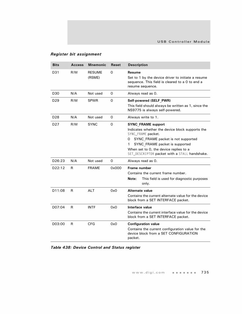
www.d i g i . com 735
USB Con t r o l l e r Modu l e
Register bit assignment
Bits Access Mnemonic Reset Description
D31 R/W RESUME(RSME)
0 ResumeSet to 1 by the device driver to initiate a resume sequence. This field is cleared to a 0 to end a resume sequence.
D30 N/A Not used 0 Always read as 0.
D29 R/W SPWR 0 Self-powered (SELF_PWR)This field should always be written as 1, since the NS9775 is always self-powered.
D28 N/A Not used 0 Always write to 1.
D27 R/W SYNC 0 SYNC_FRAME supportIndicates whether the device block supports the SYNC_FRAME packet.0 SYNC_FRAME packet is not supported1 SYNC_FRAME packet is supportedWhen set to 0, the device replies to a SET_DESCRIPTOR packet with a STALL handshake.
D26:23 N/A Not used 0 Always read as 0.
D22:12 R FRAME 0x000 Frame numberContains the current frame number.
Note: This field is used for diagnostic purposes only.
D11:08 R ALT 0x0 Alternate valueContains the current alternate value for the device block from a SET INTERFACE packet.
D07:04 R INTF 0x0 Interface valueContains the current interface value for the device block from a SET INTERFACE packet.
D03:00 R CFG 0x0 Configuration valueContains the current configuration value for the device block from a SET CONFIGURATION packet.
Table 438: Device Control and Status register
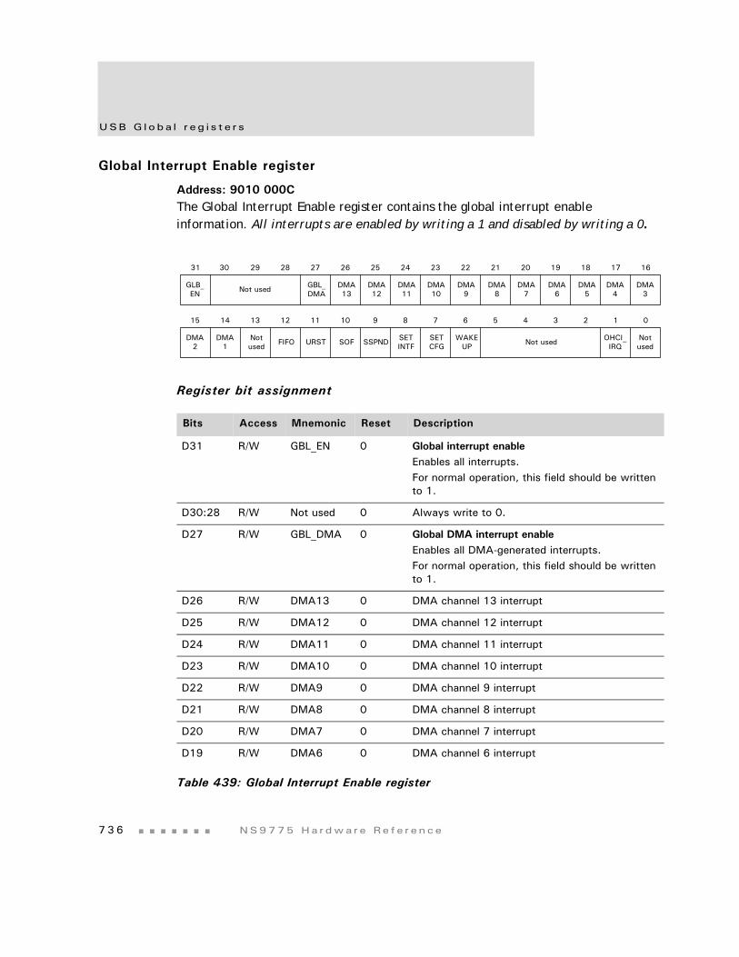
USB G l oba l r e g i s t e r s
7 3 6 NS9775 Ha r dwa r e Re f e r ence
Global Interrupt Enable register
Address: 9010 000CThe Global Interrupt Enable register contains the global interrupt enable information. All interrupts are enabled by writing a 1 and disabled by writing a 0.
Register bit assignment
Bits Access Mnemonic Reset Description
D31 R/W GBL_EN 0 Global interrupt enableEnables all interrupts.For normal operation, this field should be written to 1.
D30:28 R/W Not used 0 Always write to 0.
D27 R/W GBL_DMA 0 Global DMA interrupt enableEnables all DMA-generated interrupts.For normal operation, this field should be written to 1.
D26 R/W DMA13 0 DMA channel 13 interrupt
D25 R/W DMA12 0 DMA channel 12 interrupt
D24 R/W DMA11 0 DMA channel 11 interrupt
D23 R/W DMA10 0 DMA channel 10 interrupt
D22 R/W DMA9 0 DMA channel 9 interrupt
D21 R/W DMA8 0 DMA channel 8 interrupt
D20 R/W DMA7 0 DMA channel 7 interrupt
D19 R/W DMA6 0 DMA channel 6 interrupt
Table 439: Global Interrupt Enable register
Notused FIFO SOFURST SSPND SET
INTFSETCFG
WAKEUP Not used OHCI_
IRQNotused
13 12 11 10 9 8 7 6 5 4 3 2 1 015 14
DMA2
DMA1
31 29 28 27 26 25 24 23 22 21 20 19 18 17 1630
Not used DMA13
GBL_DMA
DMA12
DMA11
DMA10
DMA9
DMA8
DMA7
DMA6
DMA5
DMA4
DMA3
GLB_EN
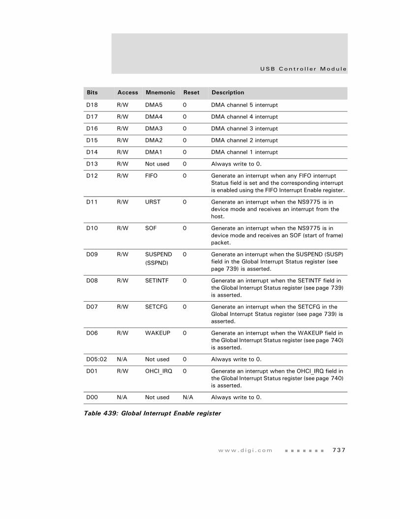
www.d i g i . com 737
USB Con t r o l l e r Modu l e
D18 R/W DMA5 0 DMA channel 5 interrupt
D17 R/W DMA4 0 DMA channel 4 interrupt
D16 R/W DMA3 0 DMA channel 3 interrupt
D15 R/W DMA2 0 DMA channel 2 interrupt
D14 R/W DMA1 0 DMA channel 1 interrupt
D13 R/W Not used 0 Always write to 0.
D12 R/W FIFO 0 Generate an interrupt when any FIFO interrupt Status field is set and the corresponding interrupt is enabled using the FIFO Interrupt Enable register.
D11 R/W URST 0 Generate an interrupt when the NS9775 is in device mode and receives an interrupt from the host.
D10 R/W SOF 0 Generate an interrupt when the NS9775 is in device mode and receives an SOF (start of frame) packet.
D09 R/W SUSPEND(SSPND)
0 Generate an interrupt when the SUSPEND (SUSP) field in the Global Interrupt Status register (see page 739) is asserted.
D08 R/W SETINTF 0 Generate an interrupt when the SETINTF field in the Global Interrupt Status register (see page 739) is asserted.
D07 R/W SETCFG 0 Generate an interrupt when the SETCFG in the Global Interrupt Status register (see page 739) is asserted.
D06 R/W WAKEUP 0 Generate an interrupt when the WAKEUP field in the Global Interrupt Status register (see page 740) is asserted.
D05:02 N/A Not used 0 Always write to 0.
D01 R/W OHCI_IRQ 0 Generate an interrupt when the OHCI_IRQ field in the Global Interrupt Status register (see page 740) is asserted.
D00 N/A Not used N/A Always write to 0.
Bits Access Mnemonic Reset Description
Table 439: Global Interrupt Enable register
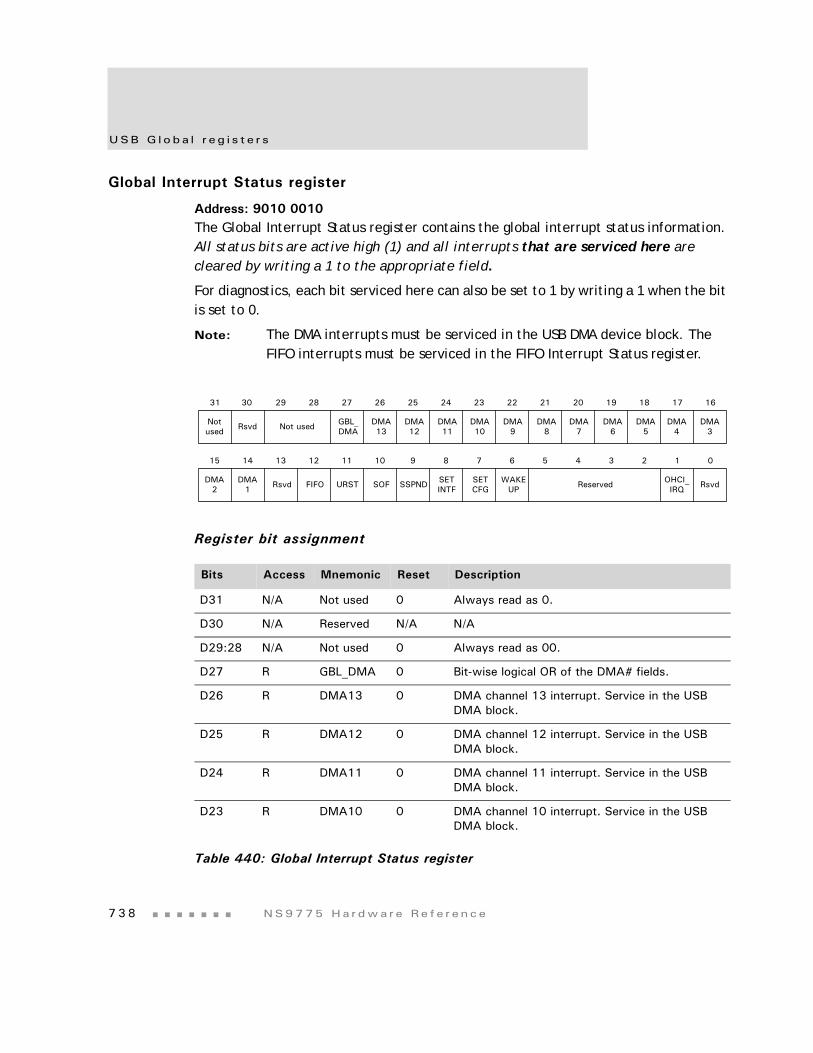
USB G l oba l r e g i s t e r s
7 3 8 NS9775 Ha r dwa r e Re f e r ence
Global Interrupt Status register
Address: 9010 0010The Global Interrupt Status register contains the global interrupt status information. All status bits are active high (1) and all interrupts that are serviced here are cleared by writing a 1 to the appropriate field.
For diagnostics, each bit serviced here can also be set to 1 by writing a 1 when the bit is set to 0.
Note: The DMA interrupts must be serviced in the USB DMA device block. The FIFO interrupts must be serviced in the FIFO Interrupt Status register.
Register bit assignment
Bits Access Mnemonic Reset Description
D31 N/A Not used 0 Always read as 0.
D30 N/A Reserved N/A N/A
D29:28 N/A Not used 0 Always read as 00.
D27 R GBL_DMA 0 Bit-wise logical OR of the DMA# fields.
D26 R DMA13 0 DMA channel 13 interrupt. Service in the USB DMA block.
D25 R DMA12 0 DMA channel 12 interrupt. Service in the USB DMA block.
D24 R DMA11 0 DMA channel 11 interrupt. Service in the USB DMA block.
D23 R DMA10 0 DMA channel 10 interrupt. Service in the USB DMA block.
Table 440: Global Interrupt Status register
Rsvd FIFO SOFURST SSPND SETINTF
SETCFG
WAKEUP Reserved OHCI_
IRQ Rsvd
13 12 11 10 9 8 7 6 5 4 3 2 1 015 14
DMA2
DMA1
31 29 28 27 26 25 24 23 22 21 20 19 18 17 1630
Not used DMA13
GBL_DMA
DMA12
DMA11
DMA10
DMA9
DMA8
DMA7
DMA6
DMA5
DMA4
DMA3
Notused Rsvd
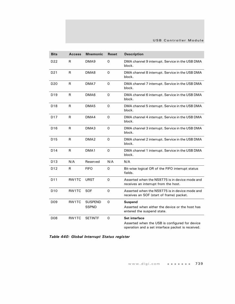
www.d i g i . com 739
USB Con t r o l l e r Modu l e
D22 R DMA9 0 DMA channel 9 interrupt. Service in the USB DMA block.
D21 R DMA8 0 DMA channel 8 interrupt. Service in the USB DMA block.
D20 R DMA7 0 DMA channel 7 interrupt. Service in the USB DMA block.
D19 R DMA6 0 DMA channel 6 interrupt. Service in the USB DMA block.
D18 R DMA5 0 DMA channel 5 interrupt. Service in the USB DMA block.
D17 R DMA4 0 DMA channel 4 interrupt. Service in the USB DMA block.
D16 R DMA3 0 DMA channel 3 interrupt. Service in the USB DMA block.
D15 R DMA2 0 DMA channel 2 interrupt. Service in the USB DMA block.
D14 R DMA1 0 DMA channel 1 interrupt. Service in the USB DMA block.
D13 N/A Reserved N/A N/A
D12 R FIFO 0 Bit-wise logical OR of the FIFO interrupt status fields.
D11 RW1TC URST 0 Asserted when the NS9775 is in device mode and receives an interrupt from the host.
D10 RW1TC SOF 0 Asserted when the NS9775 is in device mode and receives an SOF (start of frame) packet.
D09 RW1TC SUSPENDSSPND
0 SuspendAsserted when either the device or the host has entered the suspend state.
D08 RW1TC SETINTF 0 Set interfaceAsserted when the USB is configured for device operation and a set interface packet is received.
Bits Access Mnemonic Reset Description
Table 440: Global Interrupt Status register
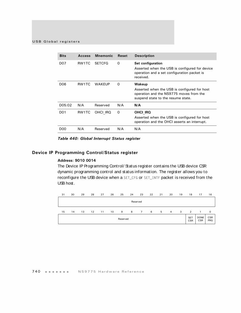
USB G l oba l r e g i s t e r s
7 4 0 NS9775 Ha r dwa r e Re f e r ence
Device IP Programming Control/Status register
Address: 9010 0014The Device IP Programming Control/Status register contains the USB device CSR dynamic programming control and status information. The register allows you to reconfigure the USB device when a SET_CFG or SET_INTF packet is received from the USB host.
D07 RW1TC SETCFG 0 Set configurationAsserted when the USB is configured for device operation and a set configuration packet is received.
D06 RW1TC WAKEUP 0 WakeupAsserted when the USB is configured for host operation and the NS9775 moves from the suspend state to the resume state.
D05:02 N/A Reserved N/A N/A
D01 RW1TC OHCI_IRQ 0 OHCI_IRQAsserted when the USB is configured for host operation and the OHCI asserts an interrupt.
D00 N/A Reserved N/A N/A
Bits Access Mnemonic Reset Description
Table 440: Global Interrupt Status register
13 12 11 10 9 8 7 6 5 4 3 2 1 015 14
31 29 28 27 26 25 24 23 22 21 20 19 18 17 1630
Reserved
Reserved SETCSR
DONECSR
CSRPRG
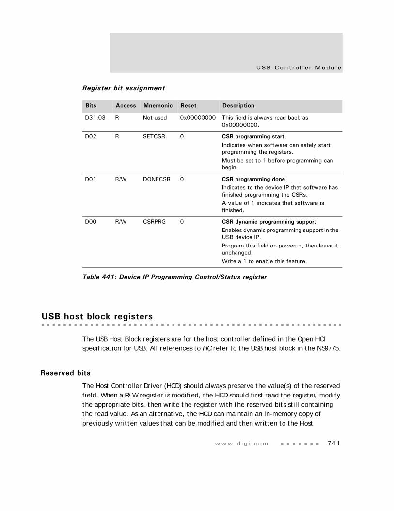
www.d i g i . com 741
USB Con t r o l l e r Modu l e
Register bit assignment
USB host block registers
The USB Host Block registers are for the host controller defined in the Open HCI specification for USB. All references to HC refer to the USB host block in the NS9775.
Reserved bits
The Host Controller Driver (HCD) should always preserve the value(s) of the reserved field. When a R/W register is modified, the HCD should first read the register, modify the appropriate bits, then write the register with the reserved bits still containing the read value. As an alternative, the HCD can maintain an in-memory copy of previously written values that can be modified and then written to the Host
Bits Access Mnemonic Reset Description
D31:03 R Not used 0x00000000 This field is always read back as 0x00000000.
D02 R SETCSR 0 CSR programming startIndicates when software can safely start programming the registers. Must be set to 1 before programming can begin.
D01 R/W DONECSR 0 CSR programming doneIndicates to the device IP that software has finished programming the CSRs.A value of 1 indicates that software is finished.
D00 R/W CSRPRG 0 CSR dynamic programming supportEnables dynamic programming support in the USB device IP. Program this field on powerup, then leave it unchanged.Write a 1 to enable this feature.
Table 441: Device IP Programming Control/Status register
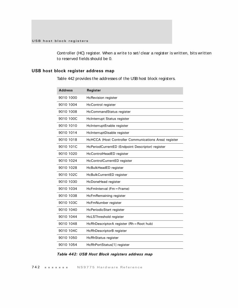
USB ho s t b l o ck r e g i s t e r s
7 4 2 NS9775 Ha r dwa r e Re f e r ence
Controller (HC) register. When a write to set/clear a register is written, bits written to reserved fields should be 0.
USB host block register address map
Table 442 provides the addresses of the USB host block registers.
Address Register
9010 1000 HcRevision register
9010 1004 HcControl register
9010 1008 HcCommandStatus register
9010 100C HcInterrupt Status register
9010 1010 HcInterruptEnable register
9010 1014 HcInterruptDisable register
9010 1018 HcHCCA (Host Controller Communications Area) register
9010 101C HcPeriodCurrentED (Endpoint Descriptor) register
9010 1020 HcControlHeadED register
9010 1024 HcControlCurrentED register
9010 1028 HcBulkHeadED register
9010 102C HcBulkCurrentED register
9010 1030 HcDoneHead register
9010 1034 HcFmInterval (Fm=Frame)
9010 1038 HcFmRemaining register
9010 103C HcFmNumber register
9010 1040 HcPeriodicStart register
9010 1044 HcLSThreshold register
9010 1048 HcRhDescriptorA register (Rh=Root hub)
9010 104C HcRhDescriptorB register
9010 1050 HcRhStatus register
9010 1054 HcRhPortStatus[1] register
Table 442: USB Host Block registers address map
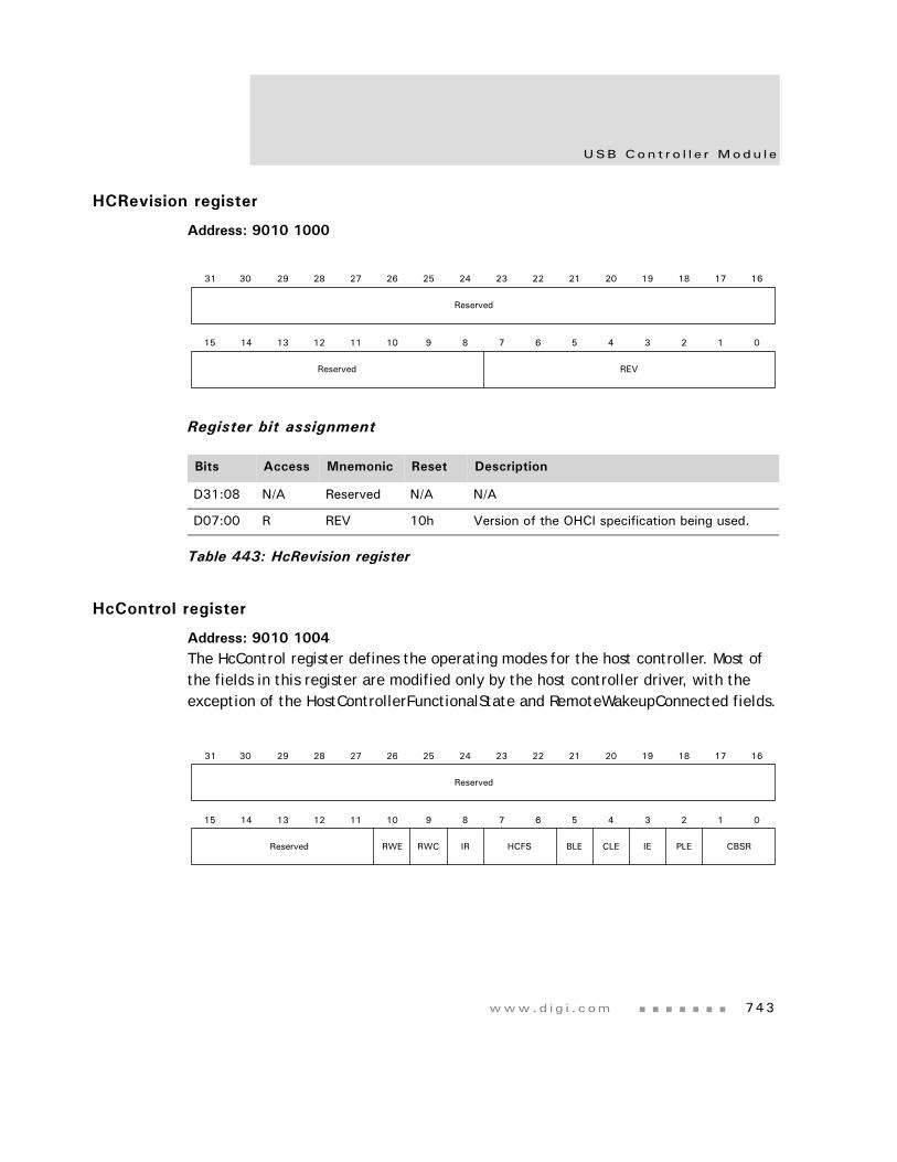
www.d i g i . com 743
USB Con t r o l l e r Modu l e
HCRevision register
Address: 9010 1000
Register bit assignment
HcControl register
Address: 9010 1004The HcControl register defines the operating modes for the host controller. Most of the fields in this register are modified only by the host controller driver, with the exception of the HostControllerFunctionalState and RemoteWakeupConnected fields.
Bits Access Mnemonic Reset Description
D31:08 N/A Reserved N/A N/A
D07:00 R REV 10h Version of the OHCI specification being used.
Table 443: HcRevision register
13 12 11 10 9 8 7 6 5 4 3 2 1 015 14
31 29 28 27 26 25 24 23 22 21 20 19 18 17 1630
Reserved
Reserved REV
13 12 11 10 9 8 7 6 5 4 3 2 1 015 14
31 29 28 27 26 25 24 23 22 21 20 19 18 17 1630
Reserved
Reserved RWE RWC IR HCFS BLE CLE IE PLE CBSR
USB ho s t b l o ck r e g i s t e r s
7 4 4 NS9775 Ha r dwa r e Re f e r ence
Register bit assignment
Bits Access Mnemonic Reset Description
D31:11 N/A Reserved N/A N/A
D10 R/W RWE 0b RemoteWakeupEnableEnables or disables the remote wakeup feature when upstream resume signaling is found. When this bit is set and the ResumeDetected bit in the HcInterruptStatus register is set, a remote wakeup is signaled to the host system.Setting this bit has no impact on the generation of hardware interrupts.
D09 R/W RWC 0b RemoteWakeupConnectedIndicates whether the host controller supports remote wakeup signaling. If remote wakeup is supported and used by the system, it is the system firmware’s responsibility to set this bit during POST. The host controller clears the bit on a hardware reset, but does not alter the bit on a software reset.
D08 R/W IR 0b InterruptRoutingDetermines the routing of interrupts generated by events registered in the HcInterruptStatus register.
If clear, all interrupts are routed to the normal host bus interrupt mechanism.
If set, interrupts are routed to the system management interrupt.
The host controller driver clears this bit on a hardware reset, but does not alter the bit on a software reset. The host controller driver uses this bit as a tag to indicate the ownership of the host controller.
Table 444: HcControl register
www.d i g i . com 745
USB Con t r o l l e r Modu l e
D07:06 R/W HCFS 00b HostControllerFunctionalState(b = binary)00b USBRESET (initial state)01b USBRESUME
10b USBOPERATIONAL
11b USBSUSPEND
A transition to USBOPERATIONAL from another state causes SOF generation to begin 1 ms later. The host controller driver can determine whether the host controller has begun sending SOFs by reading the StartofFrame field of the HcInterruptStatus register.The host controller can change this field only when in the USBSUSPEND state. The host controller can move from the USBSUSPEND state to the USBRESUME state after detecting the resume signal from a downstream port. The host controller enters the USBSUSPEND state after a software reset, whereas it enters USBRESET after a hardware reset. A hardware reset also resets the root hub, and asserts subsequent reset signaling to downstream ports.
D05 R/W BLE 0b BulkListEnableSet to enable processing of the bulk list in the next frame. If cleared by the host controller driver, the bulk list is not processed after the next SOF. The host controller checks this bit whenever it determines to process this list.When disabled, the host controller driver can modify the list. If HcBulkCurrentED is pointing to an ED to be removed, the host controller driver must advance the pointer by updating HcBulkCurrentED before re-enabling processing of the list.
Bits Access Mnemonic Reset Description
Table 444: HcControl register
USB ho s t b l o ck r e g i s t e r s
7 4 6 NS9775 Ha r dwa r e Re f e r ence
D04 R/W CLE 0b ControlListEnableSet to enable processing the control list in the next frame. If cleared by the host controller driver, the control list is not processed after the next SOF. The host controller must check this bit whenever it wants to process the list.When disabled, the host controller driver can modify the list. If HcControlCurrentED is pointing to an ED to be removed, the host controller driver must advance the pointer by updating HcControlCurrentED before re-enabling processing of the list.
D03 R/W IE 0b IsochronousEnableEnables/disables processing of the isochronous EDs. While processing the periodic list in a frame, the host controller checks the status of this bit when it finds an isochronous ED (F=1).
If set (enabled), the host controller continues processing the EDs.
If cleared (disabled), the host controller stops processing of the periodic list (which now contains only isochronous EDs) and begins processing the bulk/control lists.
Setting this bit is guaranteed to take effect in the next frame — not the current frame.
D02 R/W PLE 0b PeriodicListEnableSet to enable the processing of the periodic list in the next frame. If cleared by the host controller driver, the periodic list is not processed after the next SOF. The host controller must check this bit before it starts processing the list.
Bits Access Mnemonic Reset Description
Table 444: HcControl register
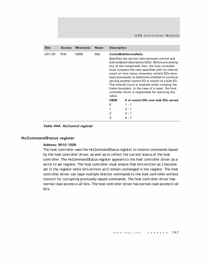
www.d i g i . com 747
USB Con t r o l l e r Modu l e
HcCommandStatus register
Address: 9010 1008The host controller uses the HcCommandStatus register to receive commands issued by the host controller driver, as well as to reflect the current status of the host controller. The HcCommandStatus register appears to the host controller driver as a write to set register. The host controller must ensure that bits written as 1 become set in the register while bits written as 0 remain unchanged in the register. The host controller driver can issue multiple distinct commands to the host controller without concern for corrupting previously-issued commands. The host controller driver has normal read access to all bits. The host controller driver has normal read access to all bits.
D01:00 R/W CBSR 00b ControlBulkServiceRatioSpecifies the service ratio between control and bulk endpoint descriptors (EDs). Before processing any of the nonperiodic lists, the host controller must compare the ratio specified with its internal count on how many nonempty control EDs have been processed, to determine whether to continue serving another control ED or switch to a bulk ED. The internal count is retained when crossing the frame boundary. In the case of a reset, the host controller driver is responsible for restoring this value.CBSR # of control EDs over bulk EDs served0 1 : 11 2 : 12 3 : 13 4 : 1
Bits Access Mnemonic Reset Description
Table 444: HcControl register
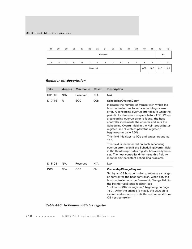
USB ho s t b l o ck r e g i s t e r s
7 4 8 NS9775 Ha r dwa r e Re f e r ence
Register bit description
Bits Access Mnemonic Reset Description
D31:18 N/A Reserved N/A N/A
D17:16 R SOC 00b SchedulingOverrunCountIndicates the number of frames with which the host controller has found a scheduling overrun error. A scheduling overrun error occurs when the periodic list does not complete before EOF. When a scheduling overrun error is found, the host controller increments the counter and sets the Scheduling Overrun field in the HcInterruptStatus register (see "HcInterruptStatus register," beginning on page 750). This field initializes to 00b and wraps around at 11b. This field is incremented on each scheduling overrun error, even if the SchedulingOverrun field in the HcInterruptStatus register has already been set. The host controller driver uses this field to monitor any persistent scheduling problems.
D15:04 N/A Reserved N/A N/A
D03 R/W OCR 0b OwnershipChangeRequestSet by an OS host controller to request a change of control for the host controller. When set, the host controller sets the OwnershipChange field in the HcInterruptStatus register (see "HcInterruptStatus register," beginning on page 750). After the change is made, the OCR bit is cleared and remains so until the next request from OS host controller.
Table 445: HcCommandStatus register
13 12 11 10 9 8 7 6 5 4 3 2 1 015 14
31 29 28 27 26 25 24 23 22 21 20 19 18 17 1630
Reserved
Reserved OCR BLF
SOC
CLF HCR
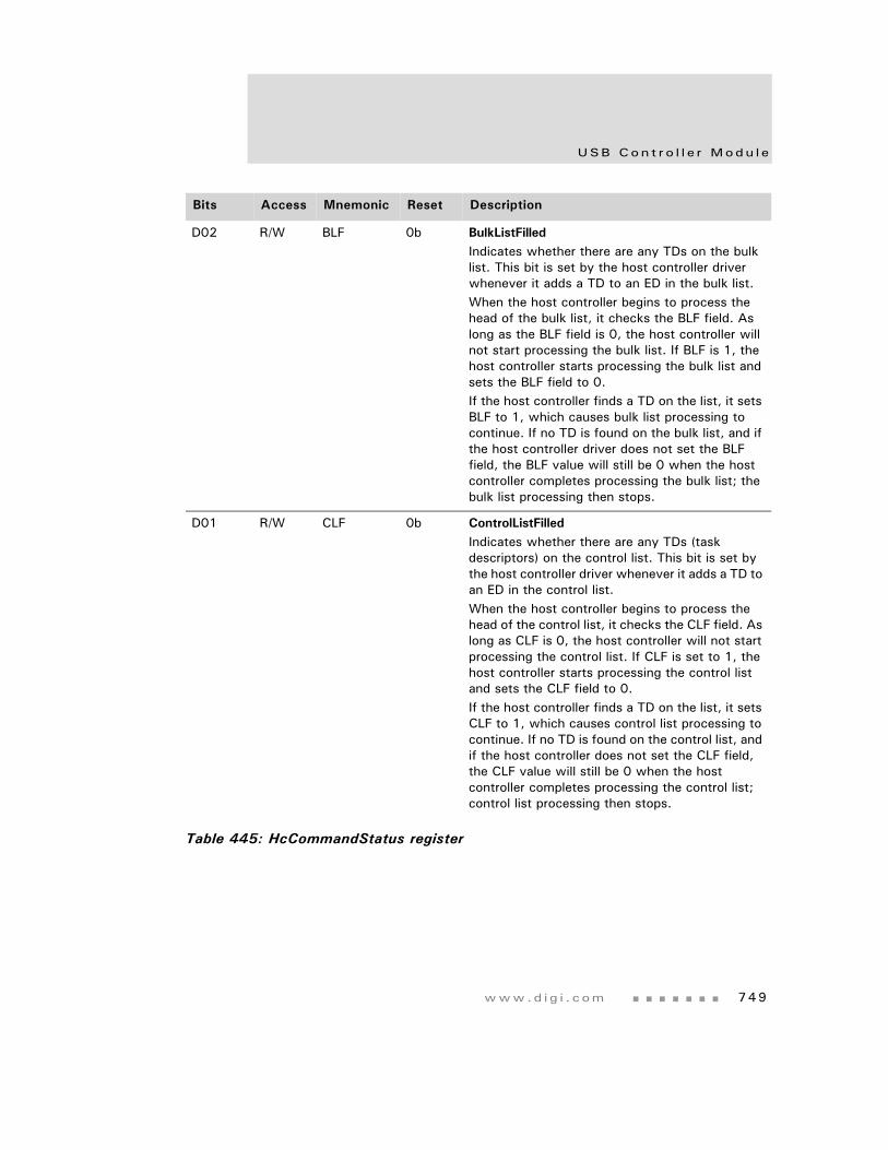
www.d i g i . com 749
USB Con t r o l l e r Modu l e
D02 R/W BLF 0b BulkListFilledIndicates whether there are any TDs on the bulk list. This bit is set by the host controller driver whenever it adds a TD to an ED in the bulk list.When the host controller begins to process the head of the bulk list, it checks the BLF field. As long as the BLF field is 0, the host controller will not start processing the bulk list. If BLF is 1, the host controller starts processing the bulk list and sets the BLF field to 0. If the host controller finds a TD on the list, it sets BLF to 1, which causes bulk list processing to continue. If no TD is found on the bulk list, and if the host controller driver does not set the BLF field, the BLF value will still be 0 when the host controller completes processing the bulk list; the bulk list processing then stops.
D01 R/W CLF 0b ControlListFilledIndicates whether there are any TDs (task descriptors) on the control list. This bit is set by the host controller driver whenever it adds a TD to an ED in the control list.When the host controller begins to process the head of the control list, it checks the CLF field. As long as CLF is 0, the host controller will not start processing the control list. If CLF is set to 1, the host controller starts processing the control list and sets the CLF field to 0. If the host controller finds a TD on the list, it sets CLF to 1, which causes control list processing to continue. If no TD is found on the control list, and if the host controller does not set the CLF field, the CLF value will still be 0 when the host controller completes processing the control list; control list processing then stops.
Bits Access Mnemonic Reset Description
Table 445: HcCommandStatus register
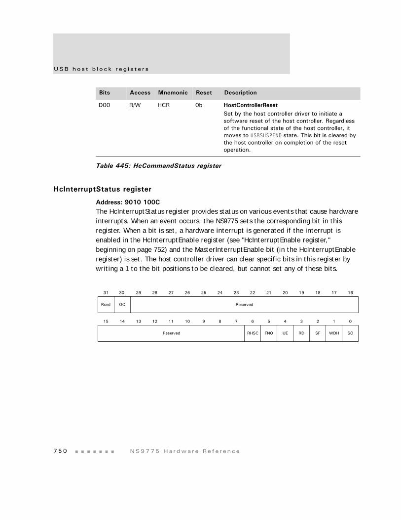
USB ho s t b l o ck r e g i s t e r s
7 5 0 NS9775 Ha r dwa r e Re f e r ence
HcInterruptStatus register
Address: 9010 100CThe HcInterruptStatus register provides status on various events that cause hardware interrupts. When an event occurs, the NS9775 sets the corresponding bit in this register. When a bit is set, a hardware interrupt is generated if the interrupt is enabled in the HcInterruptEnable register (see "HcInterruptEnable register," beginning on page 752) and the MasterInterruptEnable bit (in the HcInterruptEnable register) is set. The host controller driver can clear specific bits in this register by writing a 1 to the bit positions to be cleared, but cannot set any of these bits.
D00 R/W HCR 0b HostControllerResetSet by the host controller driver to initiate a software reset of the host controller. Regardless of the functional state of the host controller, it moves to USBSUSPEND state. This bit is cleared by the host controller on completion of the reset operation.
Bits Access Mnemonic Reset Description
Table 445: HcCommandStatus register
13 12 11 10 9 8 7 6 5 4 3 2 1 015 14
31 29 28 27 26 25 24 23 22 21 20 19 18 17 1630
RD SF WDH SO
Rsvd OC Reserved
Reserved RHSC FNO UE
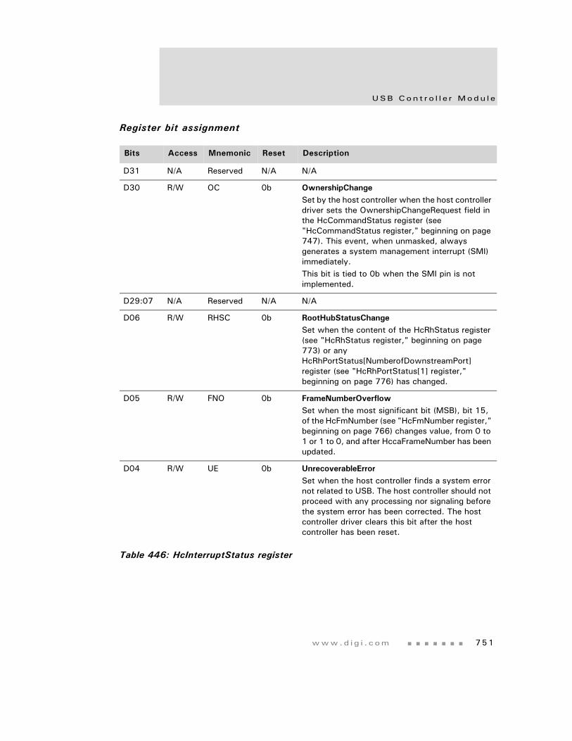
www.d i g i . com 751
USB Con t r o l l e r Modu l e
Register bit assignment
Bits Access Mnemonic Reset Description
D31 N/A Reserved N/A N/A
D30 R/W OC 0b OwnershipChangeSet by the host controller when the host controller driver sets the OwnershipChangeRequest field in the HcCommandStatus register (see "HcCommandStatus register," beginning on page 747). This event, when unmasked, always generates a system management interrupt (SMI) immediately. This bit is tied to 0b when the SMI pin is not implemented.
D29:07 N/A Reserved N/A N/A
D06 R/W RHSC 0b RootHubStatusChangeSet when the content of the HcRhStatus register (see "HcRhStatus register," beginning on page 773) or any HcRhPortStatus[NumberofDownstreamPort] register (see "HcRhPortStatus[1] register," beginning on page 776) has changed.
D05 R/W FNO 0b FrameNumberOverflowSet when the most significant bit (MSB), bit 15, of the HcFmNumber (see "HcFmNumber register," beginning on page 766) changes value, from 0 to 1 or 1 to 0, and after HccaFrameNumber has been updated.
D04 R/W UE 0b UnrecoverableErrorSet when the host controller finds a system error not related to USB. The host controller should not proceed with any processing nor signaling before the system error has been corrected. The host controller driver clears this bit after the host controller has been reset.
Table 446: HcInterruptStatus register
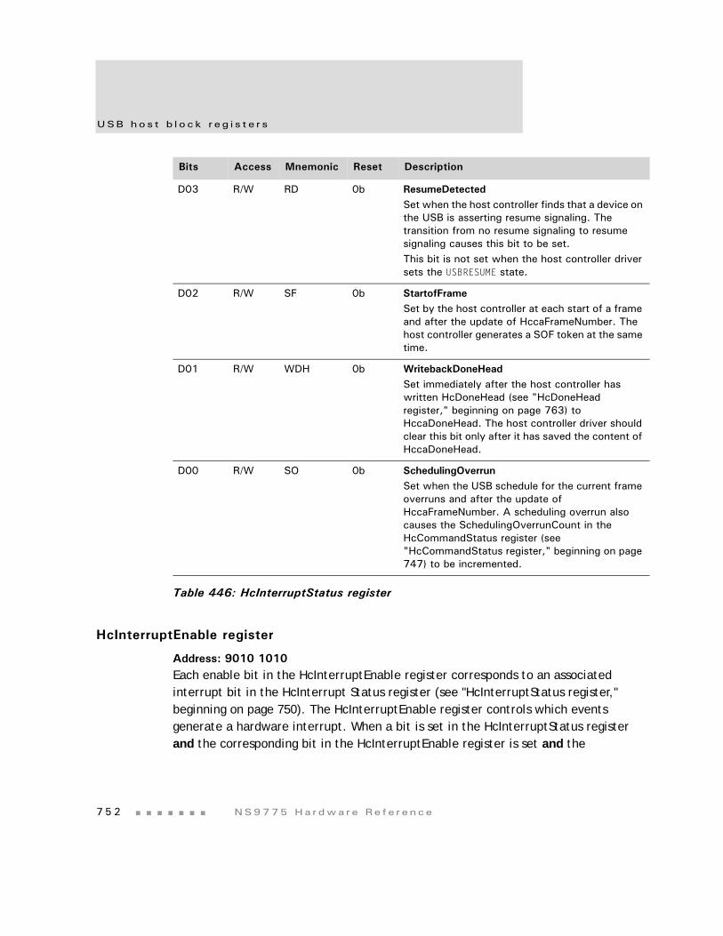
USB ho s t b l o ck r e g i s t e r s
7 5 2 NS9775 Ha r dwa r e Re f e r ence
HcInterruptEnable register
Address: 9010 1010Each enable bit in the HcInterruptEnable register corresponds to an associated interrupt bit in the HcInterrupt Status register (see "HcInterruptStatus register," beginning on page 750). The HcInterruptEnable register controls which events generate a hardware interrupt. When a bit is set in the HcInterruptStatus register and the corresponding bit in the HcInterruptEnable register is set and the
D03 R/W RD 0b ResumeDetectedSet when the host controller finds that a device on the USB is asserting resume signaling. The transition from no resume signaling to resume signaling causes this bit to be set. This bit is not set when the host controller driver sets the USBRESUME state.
D02 R/W SF 0b StartofFrameSet by the host controller at each start of a frame and after the update of HccaFrameNumber. The host controller generates a SOF token at the same time.
D01 R/W WDH 0b WritebackDoneHeadSet immediately after the host controller has written HcDoneHead (see "HcDoneHead register," beginning on page 763) to HccaDoneHead. The host controller driver should clear this bit only after it has saved the content of HccaDoneHead.
D00 R/W SO 0b SchedulingOverrunSet when the USB schedule for the current frame overruns and after the update of HccaFrameNumber. A scheduling overrun also causes the SchedulingOverrunCount in the HcCommandStatus register (see "HcCommandStatus register," beginning on page 747) to be incremented.
Bits Access Mnemonic Reset Description
Table 446: HcInterruptStatus register
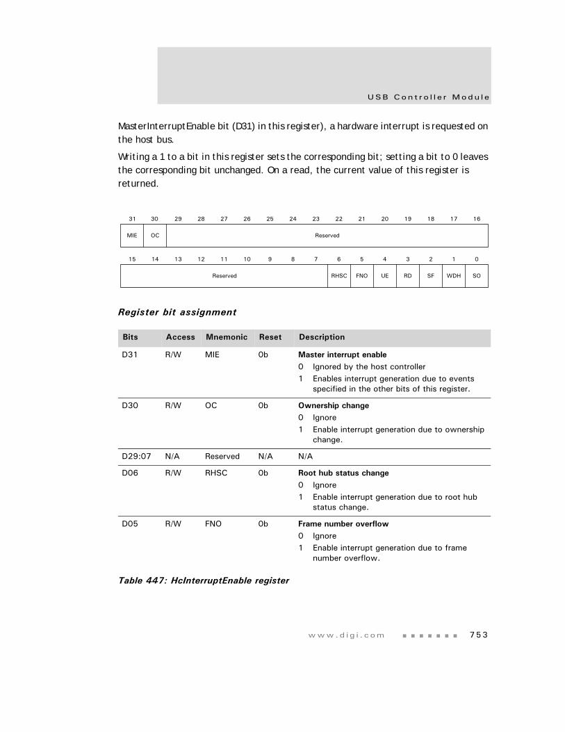
www.d i g i . com 753
USB Con t r o l l e r Modu l e
MasterInterruptEnable bit (D31) in this register), a hardware interrupt is requested on the host bus.
Writing a 1 to a bit in this register sets the corresponding bit; setting a bit to 0 leaves the corresponding bit unchanged. On a read, the current value of this register is returned.
Register bit assignment
Bits Access Mnemonic Reset Description
D31 R/W MIE 0b Master interrupt enable0 Ignored by the host controller1 Enables interrupt generation due to events
specified in the other bits of this register.
D30 R/W OC 0b Ownership change0 Ignore1 Enable interrupt generation due to ownership
change.
D29:07 N/A Reserved N/A N/A
D06 R/W RHSC 0b Root hub status change0 Ignore1 Enable interrupt generation due to root hub
status change.
D05 R/W FNO 0b Frame number overflow0 Ignore1 Enable interrupt generation due to frame
number overflow.
Table 447: HcInterruptEnable register
13 12 11 10 9 8 7 6 5 4 3 2 1 015 14
31 29 28 27 26 25 24 23 22 21 20 19 18 17 1630
RD SF WDH SO
MIE OC Reserved
Reserved RHSC FNO UE
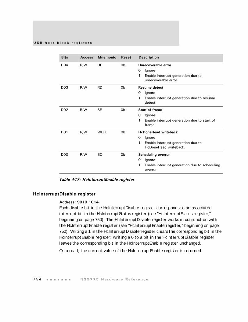
USB ho s t b l o ck r e g i s t e r s
7 5 4 NS9775 Ha r dwa r e Re f e r ence
HcInterruptDisable register
Address: 9010 1014Each disable bit in the HcInterruptDisable register corresponds to an associated interrupt bit in the HcInterruptStatus register (see "HcInterruptStatus register," beginning on page 750). The HcInterruptDisable register works in conjunction with the HcInterruptEnable register (see "HcInterruptEnable register," beginning on page 752). Writing a 1 in the HcInterruptDisable register clears the corresponding bit in the HcInterruptEnable register; writing a 0 to a bit in the HcInterruptDisable register leaves the corresponding bit in the HcInterruptEnable register unchanged.
On a read, the current value of the HcInterruptEnable register is returned.
D04 R/W UE 0b Unrecoverable error0 Ignore1 Enable interrupt generation due to
unrecoverable error.
D03 R/W RD 0b Resume detect0 Ignore1 Enable interrupt generation due to resume
detect.
D02 R/W SF 0b Start of frame0 Ignore1 Enable interrupt generation due to start of
frame.
D01 R/W WDH 0b HcDoneHead writeback0 Ignore1 Enable interrupt generation due to
HcDoneHead writeback.
D00 R/W SO 0b Scheduling overrun0 Ignore1 Enable interrupt generation due to scheduling
overrun.
Bits Access Mnemonic Reset Description
Table 447: HcInterruptEnable register
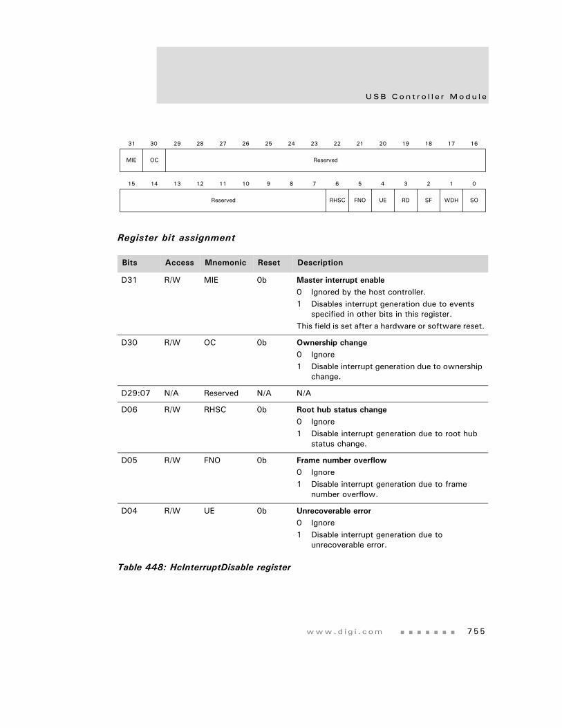
www.d i g i . com 755
USB Con t r o l l e r Modu l e
Register bit assignment
Bits Access Mnemonic Reset Description
D31 R/W MIE 0b Master interrupt enable0 Ignored by the host controller.1 Disables interrupt generation due to events
specified in other bits in this register.This field is set after a hardware or software reset.
D30 R/W OC 0b Ownership change0 Ignore1 Disable interrupt generation due to ownership
change.
D29:07 N/A Reserved N/A N/A
D06 R/W RHSC 0b Root hub status change0 Ignore1 Disable interrupt generation due to root hub
status change.
D05 R/W FNO 0b Frame number overflow0 Ignore1 Disable interrupt generation due to frame
number overflow.
D04 R/W UE 0b Unrecoverable error0 Ignore1 Disable interrupt generation due to
unrecoverable error.
Table 448: HcInterruptDisable register
13 12 11 10 9 8 7 6 5 4 3 2 1 015 14
31 29 28 27 26 25 24 23 22 21 20 19 18 17 1630
RD SF WDH SO
MIE OC Reserved
Reserved RHSC FNO UE
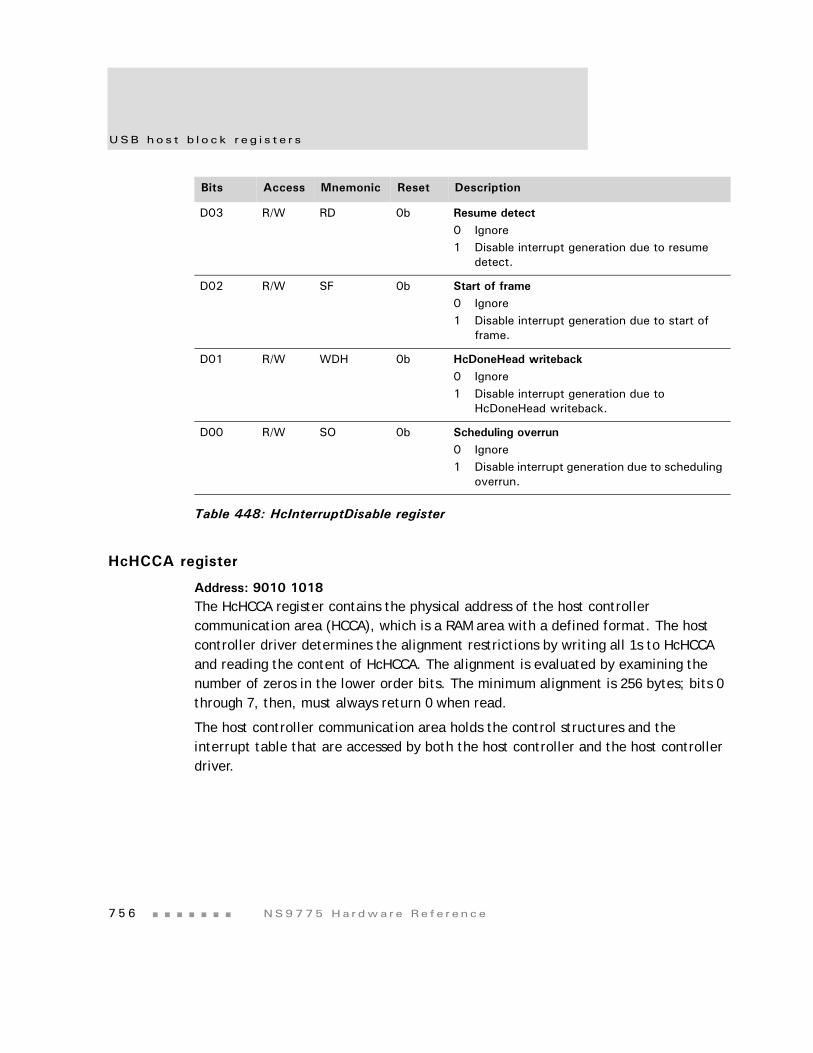
USB ho s t b l o ck r e g i s t e r s
7 5 6 NS9775 Ha r dwa r e Re f e r ence
HcHCCA register
Address: 9010 1018The HcHCCA register contains the physical address of the host controller communication area (HCCA), which is a RAM area with a defined format. The host controller driver determines the alignment restrictions by writing all 1s to HcHCCA and reading the content of HcHCCA. The alignment is evaluated by examining the number of zeros in the lower order bits. The minimum alignment is 256 bytes; bits 0 through 7, then, must always return 0 when read.
The host controller communication area holds the control structures and the interrupt table that are accessed by both the host controller and the host controller driver.
D03 R/W RD 0b Resume detect0 Ignore1 Disable interrupt generation due to resume
detect.
D02 R/W SF 0b Start of frame0 Ignore1 Disable interrupt generation due to start of
frame.
D01 R/W WDH 0b HcDoneHead writeback0 Ignore1 Disable interrupt generation due to
HcDoneHead writeback.
D00 R/W SO 0b Scheduling overrun0 Ignore1 Disable interrupt generation due to scheduling
overrun.
Bits Access Mnemonic Reset Description
Table 448: HcInterruptDisable register
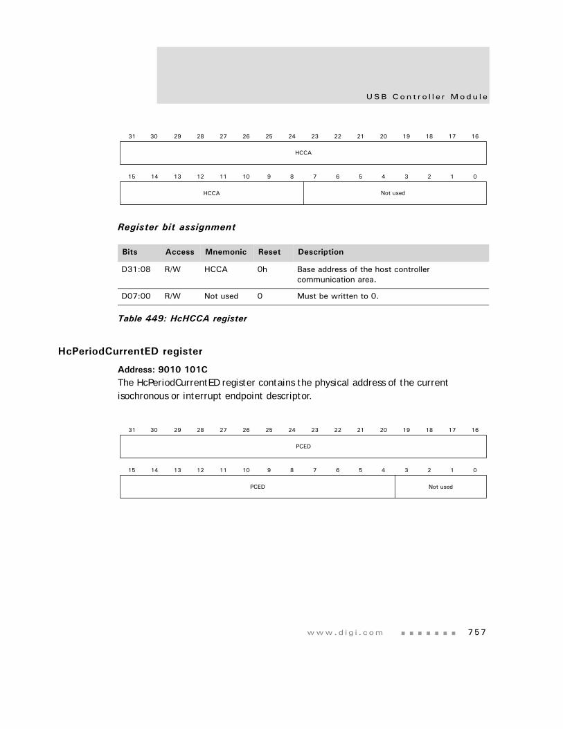
www.d i g i . com 757
USB Con t r o l l e r Modu l e
Register bit assignment
HcPeriodCurrentED register
Address: 9010 101CThe HcPeriodCurrentED register contains the physical address of the current isochronous or interrupt endpoint descriptor.
Bits Access Mnemonic Reset Description
D31:08 R/W HCCA 0h Base address of the host controller communication area.
D07:00 R/W Not used 0 Must be written to 0.
Table 449: HcHCCA register
13 12 11 10 9 8 7 6 5 4 3 2 1 015 14
31 29 28 27 26 25 24 23 22 21 20 19 18 17 1630
HCCA
Not usedHCCA
13 12 11 10 9 8 7 6 5 4 3 2 1 015 14
31 29 28 27 26 25 24 23 22 21 20 19 18 17 1630
PCED
Not usedPCED
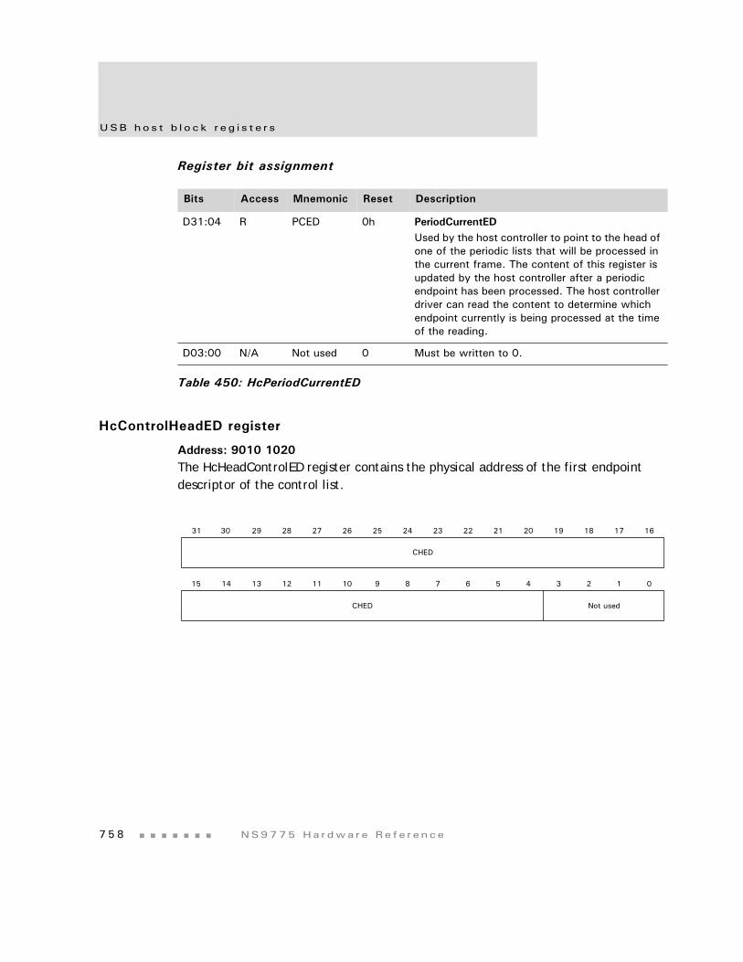
USB ho s t b l o ck r e g i s t e r s
7 5 8 NS9775 Ha r dwa r e Re f e r ence
Register bit assignment
HcControlHeadED register
Address: 9010 1020The HcHeadControlED register contains the physical address of the first endpoint descriptor of the control list.
Bits Access Mnemonic Reset Description
D31:04 R PCED 0h PeriodCurrentEDUsed by the host controller to point to the head of one of the periodic lists that will be processed in the current frame. The content of this register is updated by the host controller after a periodic endpoint has been processed. The host controller driver can read the content to determine which endpoint currently is being processed at the time of the reading.
D03:00 N/A Not used 0 Must be written to 0.
Table 450: HcPeriodCurrentED
13 12 11 10 9 8 7 6 5 4 3 2 1 015 14
31 29 28 27 26 25 24 23 22 21 20 19 18 17 1630
CHED
Not usedCHED
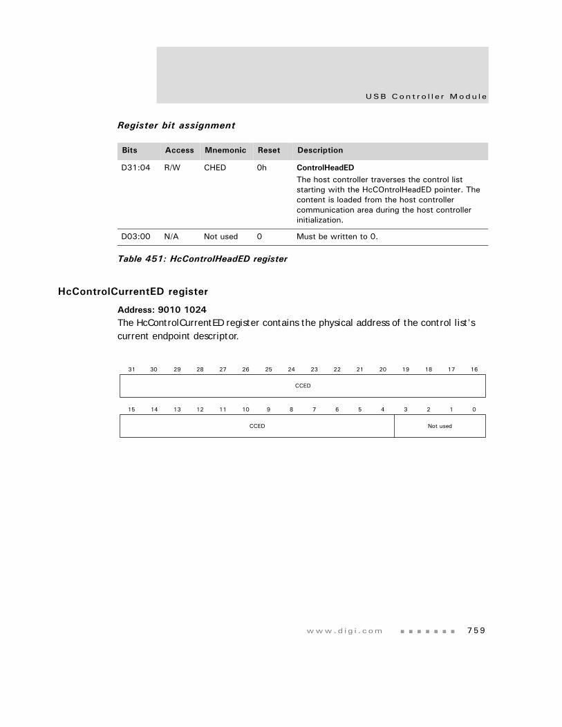
www.d i g i . com 759
USB Con t r o l l e r Modu l e
Register bit assignment
HcControlCurrentED register
Address: 9010 1024The HcControlCurrentED register contains the physical address of the control list’s current endpoint descriptor.
Bits Access Mnemonic Reset Description
D31:04 R/W CHED 0h ControlHeadEDThe host controller traverses the control list starting with the HcCOntrolHeadED pointer. The content is loaded from the host controller communication area during the host controller initialization.
D03:00 N/A Not used 0 Must be written to 0.
Table 451: HcControlHeadED register
13 12 11 10 9 8 7 6 5 4 3 2 1 015 14
31 29 28 27 26 25 24 23 22 21 20 19 18 17 1630
CCED
Not usedCCED
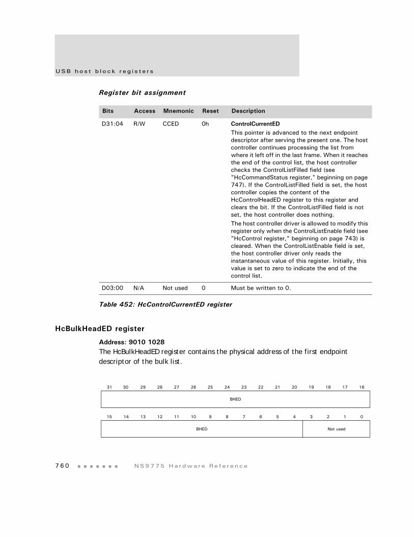
USB ho s t b l o ck r e g i s t e r s
7 6 0 NS9775 Ha r dwa r e Re f e r ence
Register bit assignment
HcBulkHeadED register
Address: 9010 1028The HcBulkHeadED register contains the physical address of the first endpoint descriptor of the bulk list.
Bits Access Mnemonic Reset Description
D31:04 R/W CCED 0h ControlCurrentEDThis pointer is advanced to the next endpoint descriptor after serving the present one. The host controller continues processing the list from where it left off in the last frame. When it reaches the end of the control list, the host controller checks the ControlListFilled field (see "HcCommandStatus register," beginning on page 747). If the ControlListFilled field is set, the host controller copies the content of the HcControlHeadED register to this register and clears the bit. If the ControlListFilled field is not set, the host controller does nothing.The host controller driver is allowed to modify this register only when the ControlListEnable field (see "HcControl register," beginning on page 743) is cleared. When the ControlListEnable field is set, the host controller driver only reads the instantaneous value of this register. Initially, this value is set to zero to indicate the end of the control list.
D03:00 N/A Not used 0 Must be written to 0.
Table 452: HcControlCurrentED register
13 12 11 10 9 8 7 6 5 4 3 2 1 015 14
31 29 28 27 26 25 24 23 22 21 20 19 18 17 1630
BHED
Not usedBHED
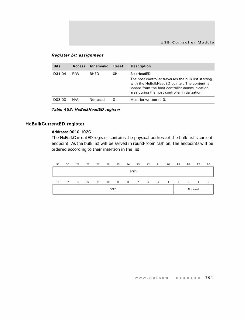
www.d i g i . com 761
USB Con t r o l l e r Modu l e
Register bit assignment
HcBulkCurrentED register
Address: 9010 102CThe HcBulkCurrentED register contains the physical address of the bulk list’s current endpoint. As the bulk list will be served in round-robin fashion, the endpoints will be ordered according to their insertion in the list.
Bits Access Mnemonic Reset Description
D31:04 R/W BHED 0h BulkHeadEDThe host controller traverses the bulk list starting with the HcBulkHeadED pointer. The content is loaded from the host controller communication area during the host controller initialization.
D03:00 N/A Not used 0 Must be written to 0.
Table 453: HcBulkHeadED register
13 12 11 10 9 8 7 6 5 4 3 2 1 015 14
31 29 28 27 26 25 24 23 22 21 20 19 18 17 1630
BCED
Not usedBCED
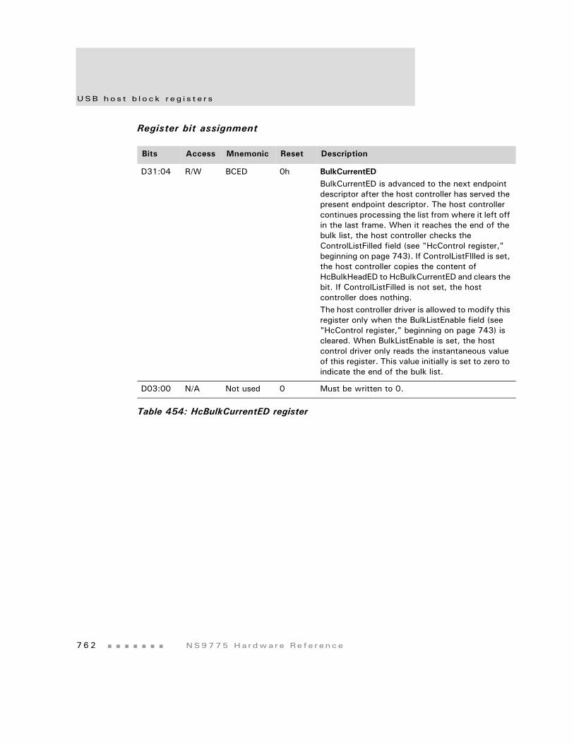
USB ho s t b l o ck r e g i s t e r s
7 6 2 NS9775 Ha r dwa r e Re f e r ence
Register bit assignment
Bits Access Mnemonic Reset Description
D31:04 R/W BCED 0h BulkCurrentEDBulkCurrentED is advanced to the next endpoint descriptor after the host controller has served the present endpoint descriptor. The host controller continues processing the list from where it left off in the last frame. When it reaches the end of the bulk list, the host controller checks the ControlListFilled field (see "HcControl register," beginning on page 743). If ControlListFIlled is set, the host controller copies the content of HcBulkHeadED to HcBulkCurrentED and clears the bit. If ControlListFilled is not set, the host controller does nothing.The host controller driver is allowed to modify this register only when the BulkListEnable field (see "HcControl register," beginning on page 743) is cleared. When BulkListEnable is set, the host control driver only reads the instantaneous value of this register. This value initially is set to zero to indicate the end of the bulk list.
D03:00 N/A Not used 0 Must be written to 0.
Table 454: HcBulkCurrentED register
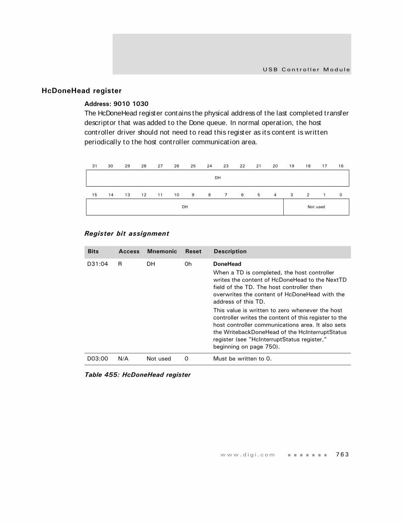
www.d i g i . com 763
USB Con t r o l l e r Modu l e
HcDoneHead register
Address: 9010 1030The HcDoneHead register contains the physical address of the last completed transfer descriptor that was added to the Done queue. In normal operation, the host controller driver should not need to read this register as its content is written periodically to the host controller communication area.
Register bit assignment
Bits Access Mnemonic Reset Description
D31:04 R DH 0h DoneHeadWhen a TD is completed, the host controller writes the content of HcDoneHead to the NextTD field of the TD. The host controller then overwrites the content of HcDoneHead with the address of this TD. This value is written to zero whenever the host controller writes the content of this register to the host controller communications area. It also sets the WritebackDoneHead of the HcInterruptStatus register (see "HcInterruptStatus register," beginning on page 750).
D03:00 N/A Not used 0 Must be written to 0.
Table 455: HcDoneHead register
13 12 11 10 9 8 7 6 5 4 3 2 1 015 14
31 29 28 27 26 25 24 23 22 21 20 19 18 17 1630
DH
Not usedDH
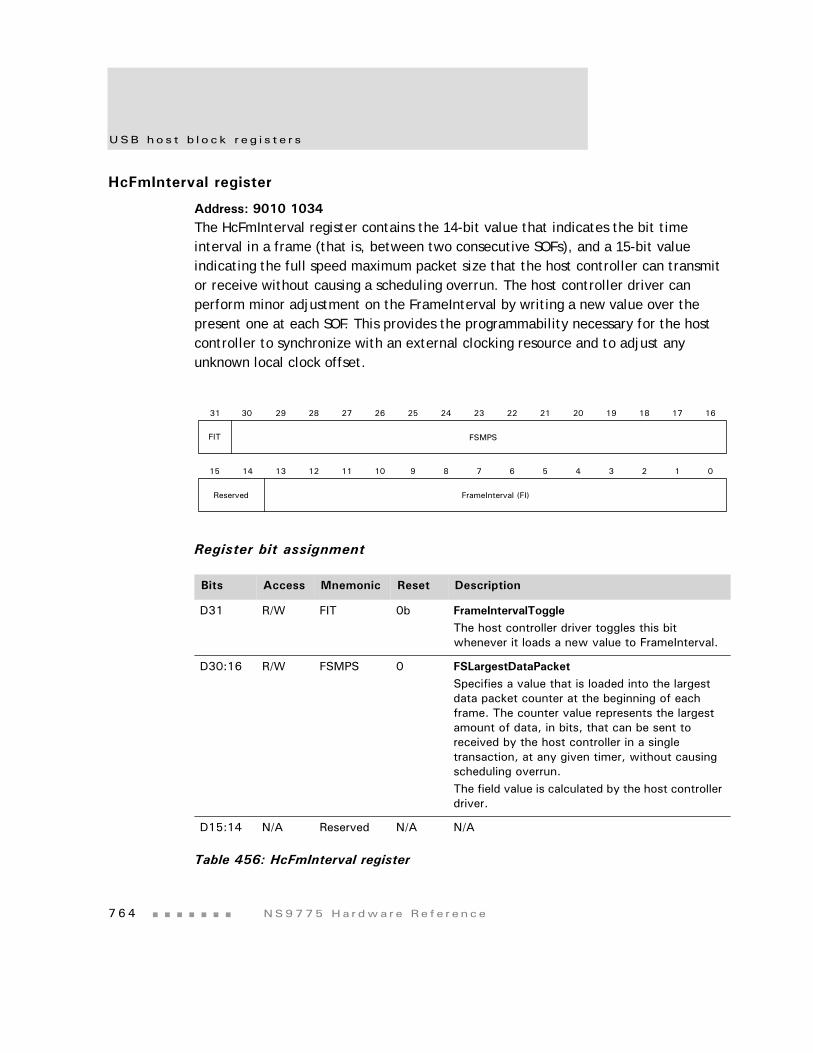
USB ho s t b l o ck r e g i s t e r s
7 6 4 NS9775 Ha r dwa r e Re f e r ence
HcFmInterval register
Address: 9010 1034The HcFmInterval register contains the 14-bit value that indicates the bit time interval in a frame (that is, between two consecutive SOFs), and a 15-bit value indicating the full speed maximum packet size that the host controller can transmit or receive without causing a scheduling overrun. The host controller driver can perform minor adjustment on the FrameInterval by writing a new value over the present one at each SOF. This provides the programmability necessary for the host controller to synchronize with an external clocking resource and to adjust any unknown local clock offset.
Register bit assignment
Bits Access Mnemonic Reset Description
D31 R/W FIT 0b FrameIntervalToggleThe host controller driver toggles this bit whenever it loads a new value to FrameInterval.
D30:16 R/W FSMPS 0 FSLargestDataPacketSpecifies a value that is loaded into the largest data packet counter at the beginning of each frame. The counter value represents the largest amount of data, in bits, that can be sent to received by the host controller in a single transaction, at any given timer, without causing scheduling overrun. The field value is calculated by the host controller driver.
D15:14 N/A Reserved N/A N/A
Table 456: HcFmInterval register
13 12 11 10 9 8 7 6 5 4 3 2 1 015 14
31 29 28 27 26 25 24 23 22 21 20 19 18 17 1630
Reserved FrameInterval (FI)
FSMPSFIT
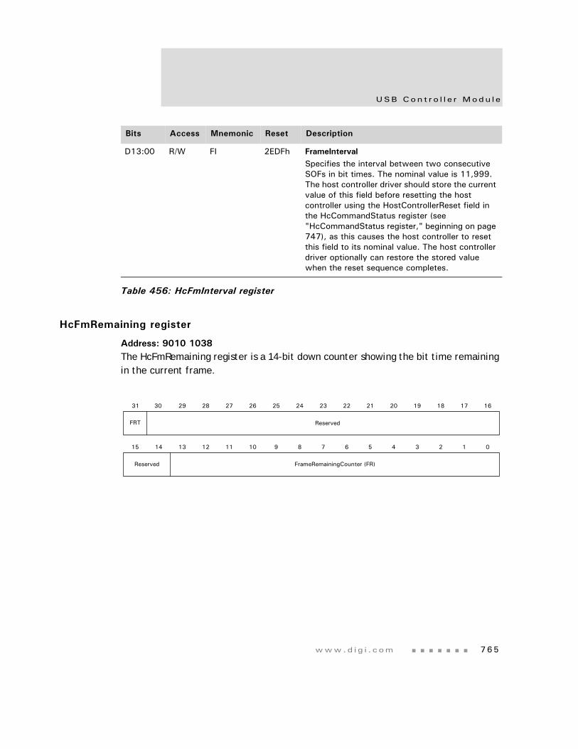
www.d i g i . com 765
USB Con t r o l l e r Modu l e
HcFmRemaining register
Address: 9010 1038The HcFmRemaining register is a 14-bit down counter showing the bit time remaining in the current frame.
D13:00 R/W FI 2EDFh FrameIntervalSpecifies the interval between two consecutive SOFs in bit times. The nominal value is 11,999. The host controller driver should store the current value of this field before resetting the host controller using the HostControllerReset field in the HcCommandStatus register (see "HcCommandStatus register," beginning on page 747), as this causes the host controller to reset this field to its nominal value. The host controller driver optionally can restore the stored value when the reset sequence completes.
Bits Access Mnemonic Reset Description
Table 456: HcFmInterval register
13 12 11 10 9 8 7 6 5 4 3 2 1 015 14
31 29 28 27 26 25 24 23 22 21 20 19 18 17 1630
Reserved FrameRemainingCounter (FR)
ReservedFRT
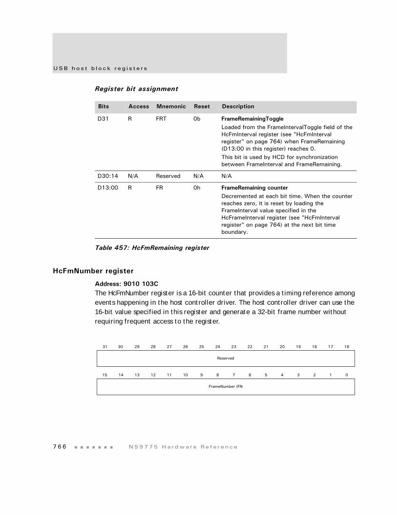
USB ho s t b l o ck r e g i s t e r s
7 6 6 NS9775 Ha r dwa r e Re f e r ence
Register bit assignment
HcFmNumber register
Address: 9010 103CThe HcFmNumber register is a 16-bit counter that provides a timing reference among events happening in the host controller driver. The host controller driver can use the 16-bit value specified in this register and generate a 32-bit frame number without requiring frequent access to the register.
Bits Access Mnemonic Reset Description
D31 R FRT 0b FrameRemainingToggleLoaded from the FrameIntervalToggle field of the HcFmInterval register (see "HcFmInterval register" on page 764) when FrameRemaining (D13:00 in this register) reaches 0. This bit is used by HCD for synchronization between FrameInterval and FrameRemaining.
D30:14 N/A Reserved N/A N/A
D13:00 R FR 0h FrameRemaining counterDecremented at each bit time. When the counter reaches zero, it is reset by loading the FrameInterval value specified in the HcFrameInterval register (see "HcFmInterval register" on page 764) at the next bit time boundary.
Table 457: HcFmRemaining register
13 12 11 10 9 8 7 6 5 4 3 2 1 015 14
31 29 28 27 26 25 24 23 22 21 20 19 18 17 1630
Reserved
FrameNumber (FN
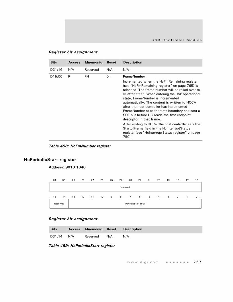
www.d i g i . com 767
USB Con t r o l l e r Modu l e
Register bit assignment
HcPeriodicStart register
Address: 9010 1040
Register bit assignment
Bits Access Mnemonic Reset Description
D31:16 N/A Reserved N/A N/A
D15:00 R FN 0h FrameNumberIncremented when the HcFmRemaining register (see "HcFmRemaining register" on page 765) is reloaded. The frame number will be rolled over to 0h after ffffh. When entering the USB operational state, FrameNumber is incremented automatically. The content is written to HCCA after the host controller has incremented FrameNumber at each frame boundary and sent a SOF but before HC reads the first endpoint descriptor in that frame. After writing to HCCa, the host controller sets the StartofFrame field in the HcInterruptStatus register (see "HcInterruptStatus register" on page 750).
Table 458: HcFmNumber register
Bits Access Mnemonic Reset Description
D31:14 N/A Reserved N/A N/A
Table 459: HcPeriodicStart register
13 12 11 10 9 8 7 6 5 4 3 2 1 015 14
31 29 28 27 26 25 24 23 22 21 20 19 18 17 1630
Reserved PeriodicStart (PS)
Reserved
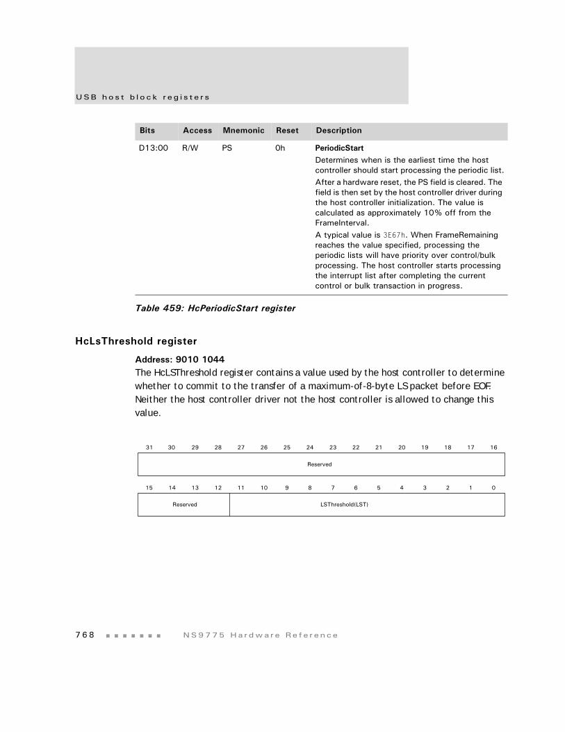
USB ho s t b l o ck r e g i s t e r s
7 6 8 NS9775 Ha r dwa r e Re f e r ence
HcLsThreshold register
Address: 9010 1044The HcLSThreshold register contains a value used by the host controller to determine whether to commit to the transfer of a maximum-of-8-byte LS packet before EOF. Neither the host controller driver not the host controller is allowed to change this value.
D13:00 R/W PS 0h PeriodicStartDetermines when is the earliest time the host controller should start processing the periodic list.After a hardware reset, the PS field is cleared. The field is then set by the host controller driver during the host controller initialization. The value is calculated as approximately 10% off from the FrameInterval. A typical value is 3E67h. When FrameRemaining reaches the value specified, processing the periodic lists will have priority over control/bulk processing. The host controller starts processing the interrupt list after completing the current control or bulk transaction in progress.
Bits Access Mnemonic Reset Description
Table 459: HcPeriodicStart register
13 12 11 10 9 8 7 6 5 4 3 2 1 015 14
31 29 28 27 26 25 24 23 22 21 20 19 18 17 1630
Reserved LSThreshold(LST)
Reserved
www.d i g i . com 769
USB Con t r o l l e r Modu l e
Register bit assignment
Root hub partition registers
The remaining USB host block registers are dedicated to the USB root hub, which is an integral part of the host controller although it is a functionally separate entity. The host controller driver emulates USBD accesses to the root hub through a register interface. The host controller driver maintains many USB-defined hub features that are not required to be supported in hardware; for example, the hub’s device configuration, interface, and endpoint descriptors are maintained only in the host controller driver as well as some status fields of the class descriptor. The host controller driver also maintains and decodes the root hub’s device address as well as performs other operations that are better suited to software than hardware.
The root hub register interface maintains similarity of bit organization and operation to typical hubs that are found in the system. The four registers defined in this section are each read and written as 32 bits. These registers are written only during initialization to correspond with system implementation.
The HcRhDescriptor A and HcRhDescriptorB registers should be implemented to be writeable, regardless of the host controller USB state.
The HcRhStatus register and HcRhPortStatus register must be writeable during the USB operational state.
Note: IS denotes an implementation-specific reset value for the related field.
Bits Access Mnemonic Reset Description
D31:12 N/A Reserved N/A N/A
D11:00 R/W LST 0628h LSThresholdContains a value that is compared to the FrameRemaining field before initiating a low speed (LS) transaction. The transaction is started only if FrameRemaining is greater than or equal to LSThreshold. The value is calculated by the host controller driver, with transmission and setup overhead considerations.
Table 460: HcLsThreshold register
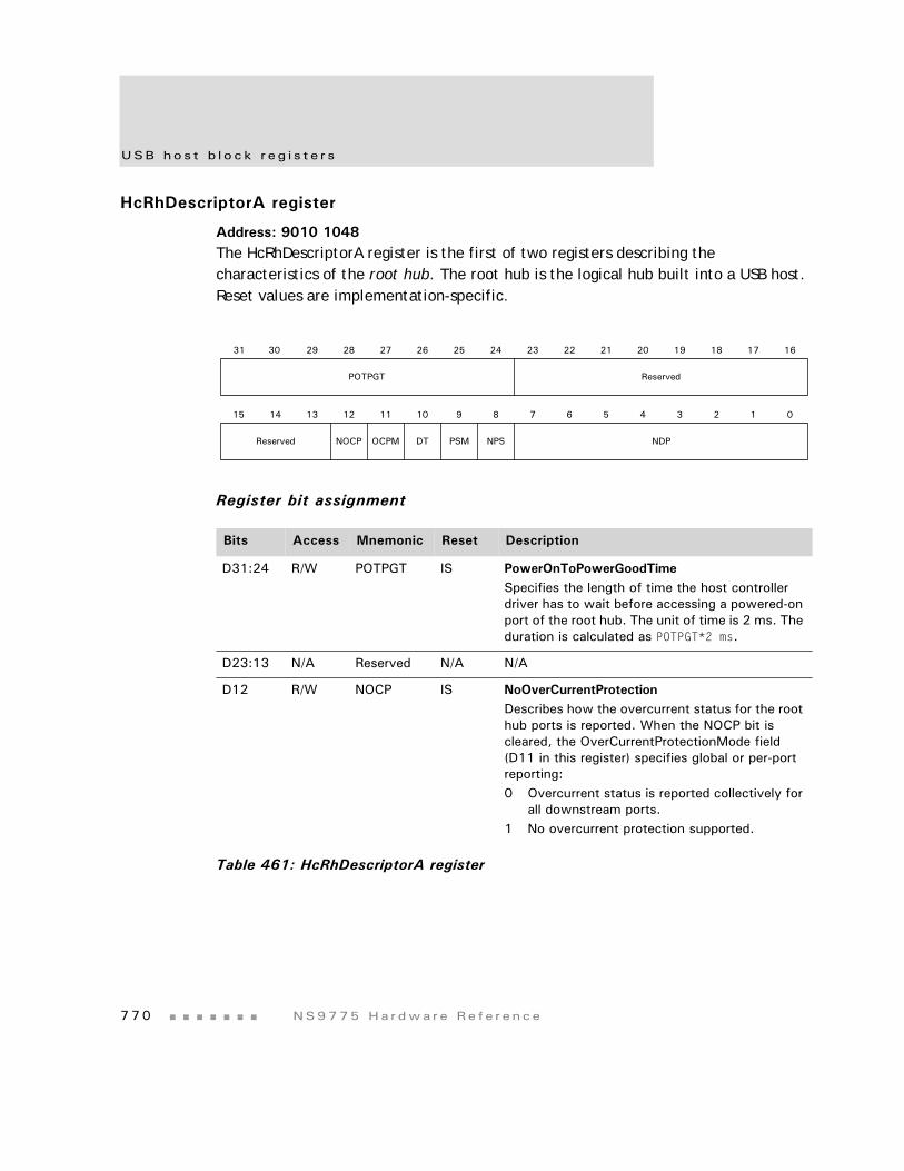
USB ho s t b l o ck r e g i s t e r s
7 7 0 NS9775 Ha r dwa r e Re f e r ence
HcRhDescriptorA register
Address: 9010 1048The HcRhDescriptorA register is the first of two registers describing the characteristics of the root hub. The root hub is the logical hub built into a USB host. Reset values are implementation-specific.
Register bit assignment
Bits Access Mnemonic Reset Description
D31:24 R/W POTPGT IS PowerOnToPowerGoodTimeSpecifies the length of time the host controller driver has to wait before accessing a powered-on port of the root hub. The unit of time is 2 ms. The duration is calculated as POTPGT*2 ms.
D23:13 N/A Reserved N/A N/A
D12 R/W NOCP IS NoOverCurrentProtectionDescribes how the overcurrent status for the root hub ports is reported. When the NOCP bit is cleared, the OverCurrentProtectionMode field (D11 in this register) specifies global or per-port reporting:0 Overcurrent status is reported collectively for
all downstream ports.1 No overcurrent protection supported.
Table 461: HcRhDescriptorA register
NDP
13 12 11 10 9 8 7 6 5 4 3 2 1 015 14
31 29 28 27 26 25 24 23 22 21 20 19 18 17 1630
POTPGT
Reserved
Reserved
NOCP OCPM DT PSM NPS
www.d i g i . com 771
USB Con t r o l l e r Modu l e
D11 R/W OCPM IS OverCurrentProtectionModeDescribes how the overcurrent status for the root hub ports is reported. At reset, this field should reflect the same mode as PowerSwitchingMode (D08 in this register). The OCPM field is valid only if the NoOverCurrentProtection field (D12 in this register) is cleared. 0 Overcurrent status is reported collectively for
all downstream ports.1 Overcurrent status is reported on a per-port
basis.
D10 R DT 0b Device typeSpecifies that the root hub is not a compound device. The root hub is not allowed to be a compound device. This field should always read 0.
D09 R/W PSM IS PowerSwitchingModeSpecifies how the power switching of the root hubs is controlled. This field is valid only if the NoPowerSwitching field (D08 in this register) is cleared.0 All ports are powered at the same time.1 Each port is powered individually. This mode
allows port power to be controlled by either the global switch or per-port switching. If the PortPowerControlMask bit (see "HcRhDescriptorB register" on page 772) is set, the port responds only to port power commands (Set/ClearPortPower). If the port mask is cleared, the port is controlled only by the global power switch (Set/ClearGlobalPower).
D08 R/W NPS IS NoPowerSwitchingSpecifies whether power switching is supported or ports are always powered. When this bit is cleared, the PowerSwitchingMode (D09 in this register) specifies global or per-port switching.0 Ports are power switched.1 Ports are always powered on when the host
controller is powered on.
Bits Access Mnemonic Reset Description
Table 461: HcRhDescriptorA register
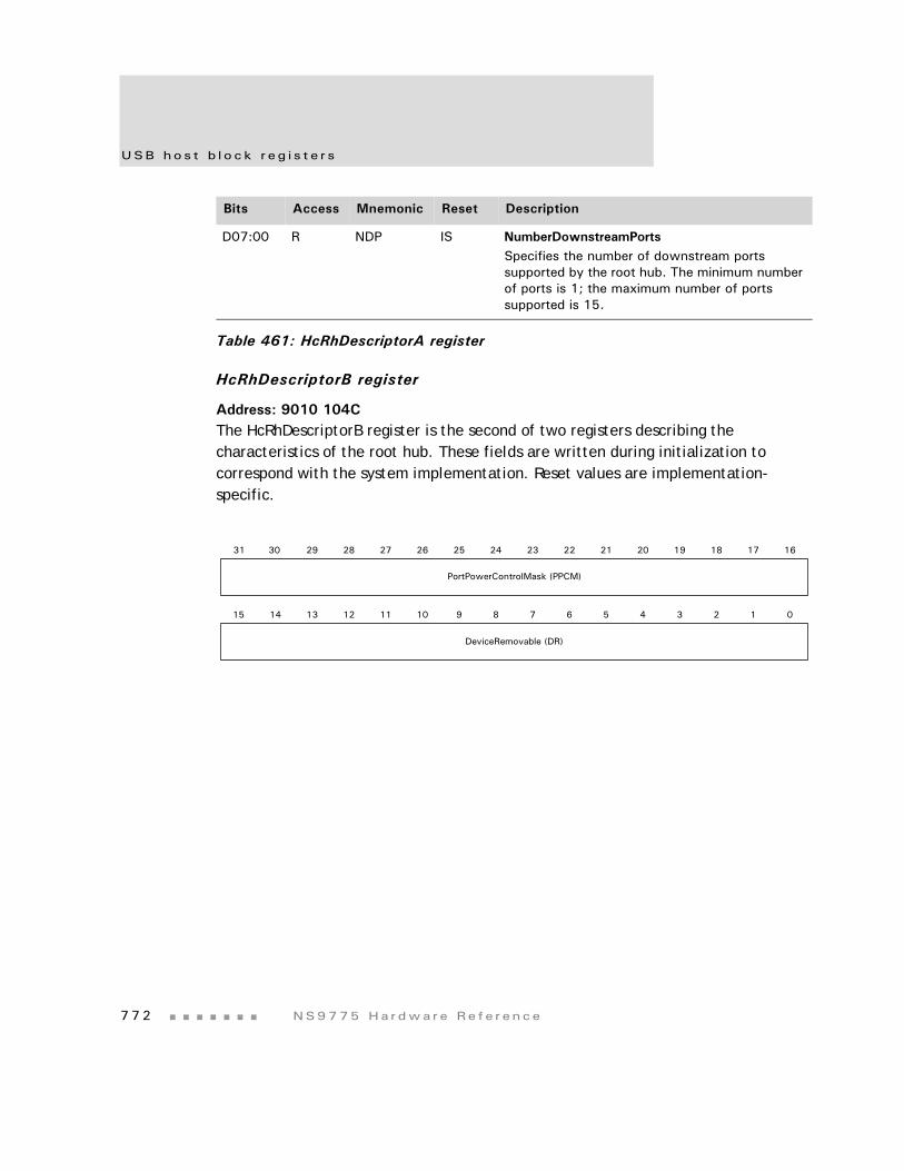
USB ho s t b l o ck r e g i s t e r s
7 7 2 NS9775 Ha r dwa r e Re f e r ence
HcRhDescriptorB register
Address: 9010 104CThe HcRhDescriptorB register is the second of two registers describing the characteristics of the root hub. These fields are written during initialization to correspond with the system implementation. Reset values are implementation-specific.
D07:00 R NDP IS NumberDownstreamPortsSpecifies the number of downstream ports supported by the root hub. The minimum number of ports is 1; the maximum number of ports supported is 15.
Bits Access Mnemonic Reset Description
Table 461: HcRhDescriptorA register
13 12 11 10 9 8 7 6 5 4 3 2 1 015 14
31 29 28 27 26 25 24 23 22 21 20 19 18 17 1630
PortPowerControlMask (PPCM)
DeviceRemovable (DR)
www.d i g i . com 773
USB Con t r o l l e r Modu l e
Register bit assignment
HcRhStatus register
Address: 9010 1050The HcRhStatus register has two parts:
The lower word of a Dword represents the hub status field.
The upper word of the Dword represents the hub status change field.
Bits Access Mnemonic Reset Description
D31:16 R/W PPCM IS PortPowerControlMaskEach bit indicates whether a port is affected by a global control command when PowerSwitchingMode (see "HcRhDescriptorA register" on page 770) is set. When set, the port’s power state is affected only by per-port power control (Set/ClearPortPower). When cleared, the port is controlled by the global power switch (Set/ClearGlobalPower). If the device is configured to global switching mode (PowerSwitchingMode=0), this field is not valid.Bit 0: ReservedBit 1: Ganged-power mask on port #1Bit 2: Ganged-power mask on port #2...Bit 15: Ganged-power mask on port #15
D15:00 R/W DR IS DeviceRemovableEach bit is dedicated to a root hub port.
When cleared, the attached device is removable.
When set, the attached device is not removable.
Bit 0: ReservedBit 1: Device attached to port #1Bit 2: Device attached to port #2...Bit 15: device attached to port #15
Table 462: HcRhDesdcriptorB register
USB ho s t b l o ck r e g i s t e r s
7 7 4 NS9775 Ha r dwa r e Re f e r ence
Register bit assignment
Bits Access Mnemonic Reset Description
D31 W CRWE N/A ClearRemoteWakeupEnable0 Has no effect1 Clears DeviceRemoveWakeupEnable
D30:18 N/A Not used N/A Always write to 0.
D17 R/W CCIC 0b OverCurrentIndicatorChangeSet by hardware when a change has occurred to the OCI field (bit 01 in this register). The host controller driver clears this bit by writing 1. Writing 0 to this bit has no effect.
D16 R/W LPSC 0b LocalPowerStatusChange (LPSC)Not supported; always read as 0.
SetGlobalPower (write)In global power mode (PowerSwitchingMode=0), this bit is written to 1 to turn on power to all ports (clear PowerPortStatus).
In per-port mode, this bit sets PortPowerStatus only on ports whose PortPowerControlMask bit is not set.
Writing 0 to this bit has no effect
Table 463: HcRhStatus register
13 12 11 10 9 8 7 6 5 4 3 2 1 015 14
31 29 28 27 26 25 24 23 22 21 20 19 18 17 1630
Not usedCRWE CCIC LPSC
DRWE Not used OCI LPS
www.d i g i . com 775
USB Con t r o l l e r Modu l e
D15 R/W DRWE 0b DeviceRemoteWakeupEnable (read)Enables a ConnectStatusChange bit as a resume event, causing a USBSUSPEND or USBRESUME state transition and setting the ResumeDetected interrupt.0 ConnectStatusChange is not a remote
wakeup event1 ConnectStatusChange is a remote wakeup
event.
SetRemoteWakeupEnable (write)0 Has no effect1 Sets DeviceRemoteWakeupEnable
D14:02 N/A Not used N/A Always write to 0.
D01 R OCI 0b OverCurrentIndicatorReports overcurrent conditions when global reporting is implemented.
When set, an overcurrent condition exists.
When cleared, all power operations are normal.
If per-port overcurrent is implemented, this bit is always 0.
D00 R/W LPS 0b LocalPowerStatus (read)Not supported; always read as 0.
ClearGlobalPower (write)In global power mode (PowerSwitchingMode=0), this bit is always written to 1 to turn off power to all ports (clear PowerPortStatus).In per-port power mode, this bit clears PortPowerStatus only on ports whose PortPowerControlMask bit is not set. Writing 0 to this bit has no effect.
Bits Access Mnemonic Reset Description
Table 463: HcRhStatus register
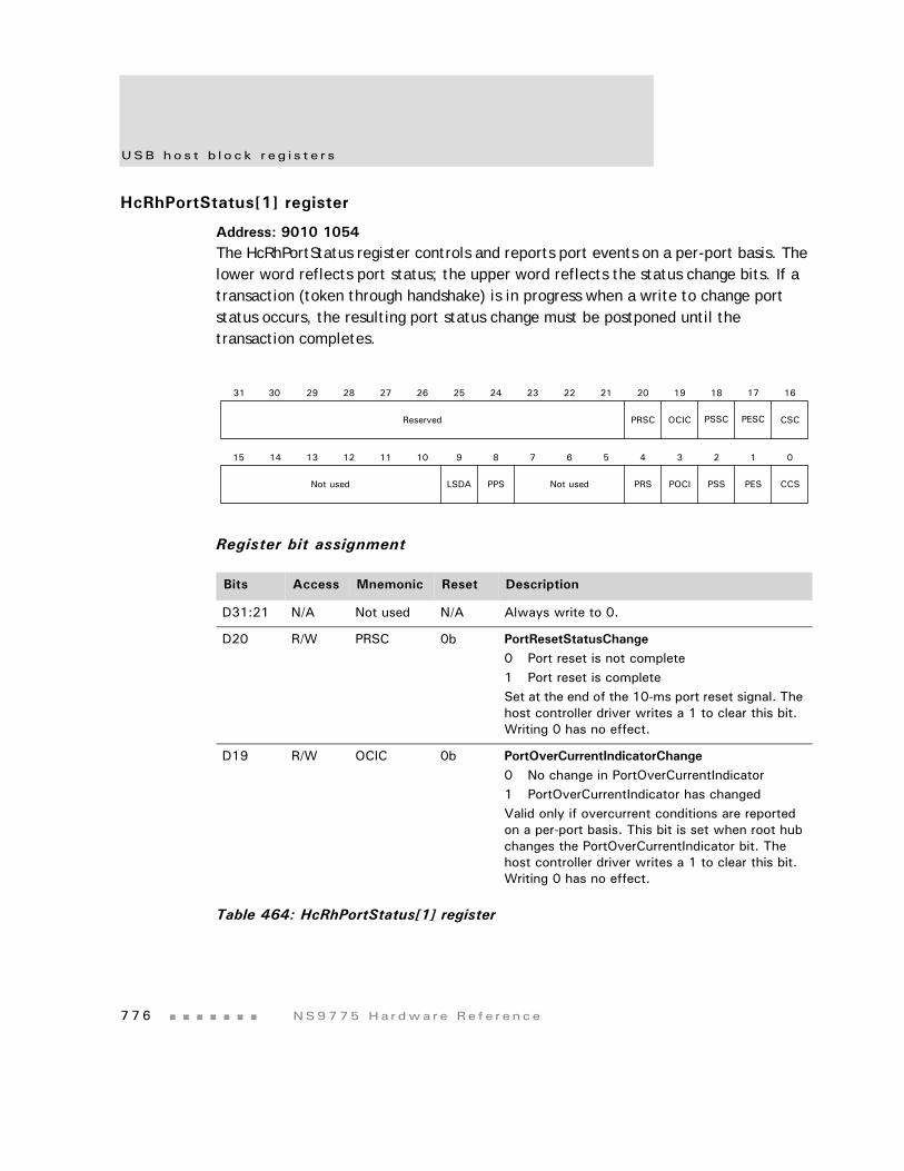
USB ho s t b l o ck r e g i s t e r s
7 7 6 NS9775 Ha r dwa r e Re f e r ence
HcRhPortStatus[1] register
Address: 9010 1054The HcRhPortStatus register controls and reports port events on a per-port basis. The lower word reflects port status; the upper word reflects the status change bits. If a transaction (token through handshake) is in progress when a write to change port status occurs, the resulting port status change must be postponed until the transaction completes.
Register bit assignment
Bits Access Mnemonic Reset Description
D31:21 N/A Not used N/A Always write to 0.
D20 R/W PRSC 0b PortResetStatusChange0 Port reset is not complete1 Port reset is completeSet at the end of the 10-ms port reset signal. The host controller driver writes a 1 to clear this bit. Writing 0 has no effect.
D19 R/W OCIC 0b PortOverCurrentIndicatorChange0 No change in PortOverCurrentIndicator1 PortOverCurrentIndicator has changedValid only if overcurrent conditions are reported on a per-port basis. This bit is set when root hub changes the PortOverCurrentIndicator bit. The host controller driver writes a 1 to clear this bit. Writing 0 has no effect.
Table 464: HcRhPortStatus[1] register
13 12 11 10 9 8 7 6 5 4 3 2 1 015 14
31 29 28 27 26 25 24 23 22 21 20 19 18 17 1630
Reserved PRSC PESC CSC
Not used PES CCS
OCIC PSSC
LSDA PPS Not used PRS POCI PSS
www.d i g i . com 777
USB Con t r o l l e r Modu l e
D18 R/W PSSC 0b PortSuspendStatusChange0 Resume is not completed1 Resume completedSet when the full resume sequence has been completed. This sequence includes the 20-s resume pulse, LS EOP, and 3-ms resynchronization delay. The host controller driver writes a 1 to clear this bit. Writing 0 has no effect. This bit also is cleared when ResetStatusChange is set.
D17 R/W PESC 0b PortEnableStatusChange0 No change in PortEnableStatus1 Change in PortEnableStatusSet when hardware events cause the PortEnableStatus bit to be cleared. Changes from host controller driver writes do not set this bit. The host controller driver writes a 1 to clear this bit. Writing 0 has no effect.
D16 R/W CSC 0b ConnectStatusChange0 No change in CurrentConnectStatus1 Change in CurrentConnectStatusSet when a connect or disconnect event occurs. The host controller driver writes a 1 to clear this bit. Writing 0 has no effect. If CurrentConnectStatus is cleared when a SetPortReset, SetPortEnable, or SetPortSuspend write occurs, this bit is set to force the driver to re-evaluate the connection status, as these writes should not occur if the port is disconnected.
Note: If the DeviceRemovable[NDP] bit is set, the CSC bit is set only after a root hub reset, to tell the system that the device is attached.
D15:10 N/A Not used N/A Always write to 0.
Bits Access Mnemonic Reset Description
Table 464: HcRhPortStatus[1] register
USB ho s t b l o ck r e g i s t e r s
7 7 8 NS9775 Ha r dwa r e Re f e r ence
D09 R/W LSDA Xb LowSpeedDeviceAttached (read)0 Full speed device attached1 Low speed device attachedIndicates the speed of the device attached to this port. When set, the low speed device is attached to this port. When clear, a full speed device is attached to this port. This field is valid only when CurrentConnectStatus is set.ClearPortPower (write)The host controller driver clears the PortPowerStatus bit by writing a 1 to this bit. Writing 0 has no effect.
D08 R/W PPS 0b PortPowerStatus (read)0 Port power is off1 Port power is onReflects the port’s power status, regardless of the type of power switching implemented. This bit is cleared is an overcurrent condition is found. The host controller driver sets this bit by writing SetPortPower or SetGlobalPower. The host controller driver clears this bit by writing ClearPortPower or ClearGlobalPower. PowerSwitchingMode and PortPowerControlMask determine which switches are enabled.
In global switching mode, (PowerSwitchingMode=0), only Set/ClearGlobalPower controls this bit.
In per-port power switching (PowerSwitchingMode=1), if the PortPowerControlMask bit is set, only Set/ClearPortPower commands are enabled. If the mask is not set, only Set/ClearGlobalPower commands are enabled. When port power is disabled, CurrentConnectStatus, PortEnableStatus, PortSuspendStatus, and PortResetStatus should be reset.
Bits Access Mnemonic Reset Description
Table 464: HcRhPortStatus[1] register
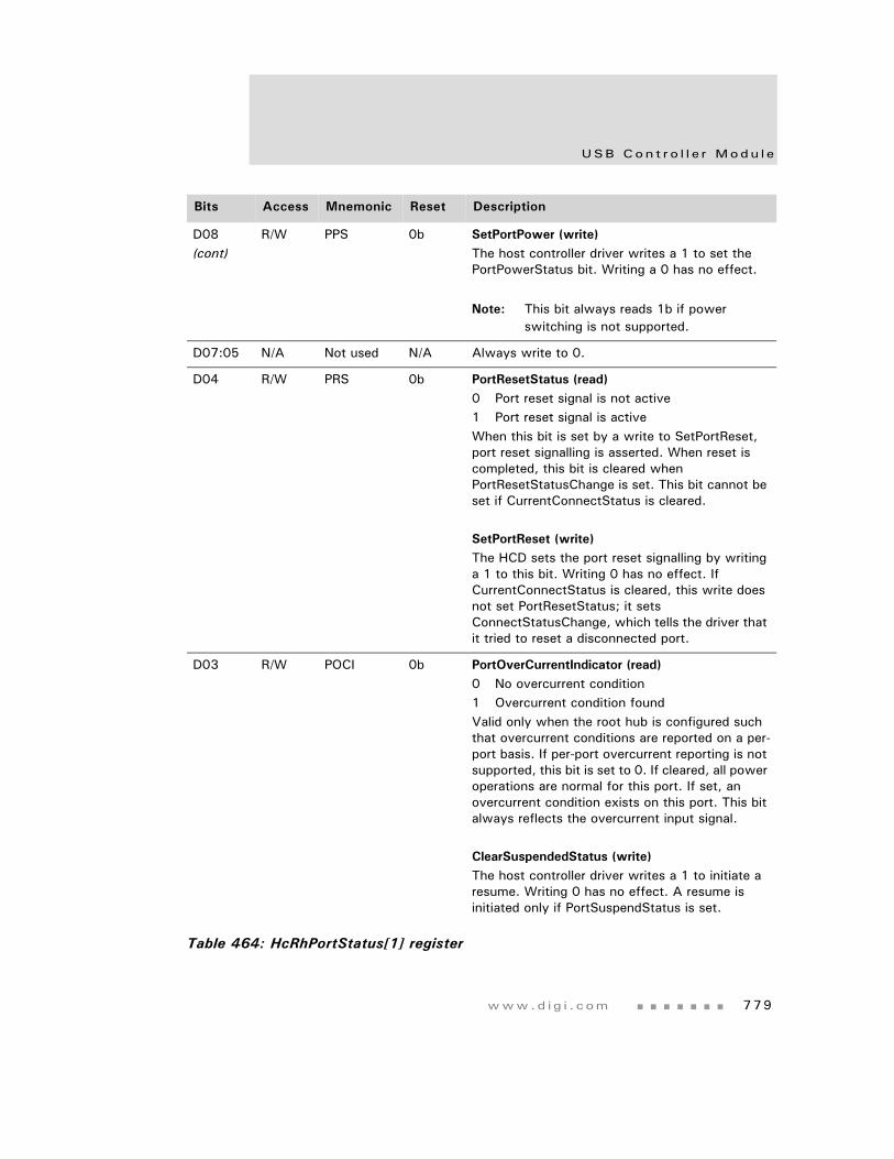
www.d i g i . com 779
USB Con t r o l l e r Modu l e
D08(cont)
R/W PPS 0b SetPortPower (write)The host controller driver writes a 1 to set the PortPowerStatus bit. Writing a 0 has no effect.
Note: This bit always reads 1b if power switching is not supported.
D07:05 N/A Not used N/A Always write to 0.
D04 R/W PRS 0b PortResetStatus (read)0 Port reset signal is not active1 Port reset signal is activeWhen this bit is set by a write to SetPortReset, port reset signalling is asserted. When reset is completed, this bit is cleared when PortResetStatusChange is set. This bit cannot be set if CurrentConnectStatus is cleared.
SetPortReset (write)The HCD sets the port reset signalling by writing a 1 to this bit. Writing 0 has no effect. If CurrentConnectStatus is cleared, this write does not set PortResetStatus; it sets ConnectStatusChange, which tells the driver that it tried to reset a disconnected port.
D03 R/W POCI 0b PortOverCurrentIndicator (read)0 No overcurrent condition1 Overcurrent condition foundValid only when the root hub is configured such that overcurrent conditions are reported on a per-port basis. If per-port overcurrent reporting is not supported, this bit is set to 0. If cleared, all power operations are normal for this port. If set, an overcurrent condition exists on this port. This bit always reflects the overcurrent input signal.
ClearSuspendedStatus (write)The host controller driver writes a 1 to initiate a resume. Writing 0 has no effect. A resume is initiated only if PortSuspendStatus is set.
Bits Access Mnemonic Reset Description
Table 464: HcRhPortStatus[1] register
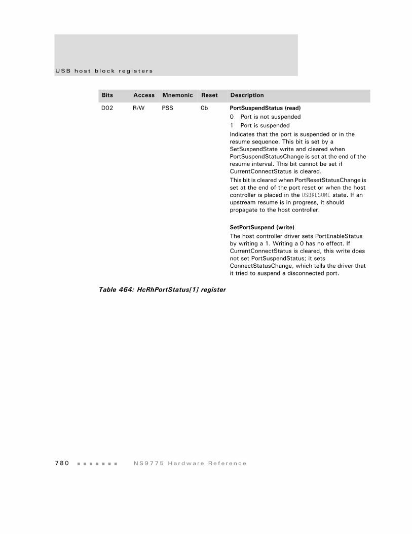
USB ho s t b l o ck r e g i s t e r s
7 8 0 NS9775 Ha r dwa r e Re f e r ence
D02 R/W PSS 0b PortSuspendStatus (read)0 Port is not suspended1 Port is suspendedIndicates that the port is suspended or in the resume sequence. This bit is set by a SetSuspendState write and cleared when PortSuspendStatusChange is set at the end of the resume interval. This bit cannot be set if CurrentConnectStatus is cleared. This bit is cleared when PortResetStatusChange is set at the end of the port reset or when the host controller is placed in the USBRESUME state. If an upstream resume is in progress, it should propagate to the host controller.
SetPortSuspend (write)The host controller driver sets PortEnableStatus by writing a 1. Writing a 0 has no effect. If CurrentConnectStatus is cleared, this write does not set PortSuspendStatus; it sets ConnectStatusChange, which tells the driver that it tried to suspend a disconnected port.
Bits Access Mnemonic Reset Description
Table 464: HcRhPortStatus[1] register
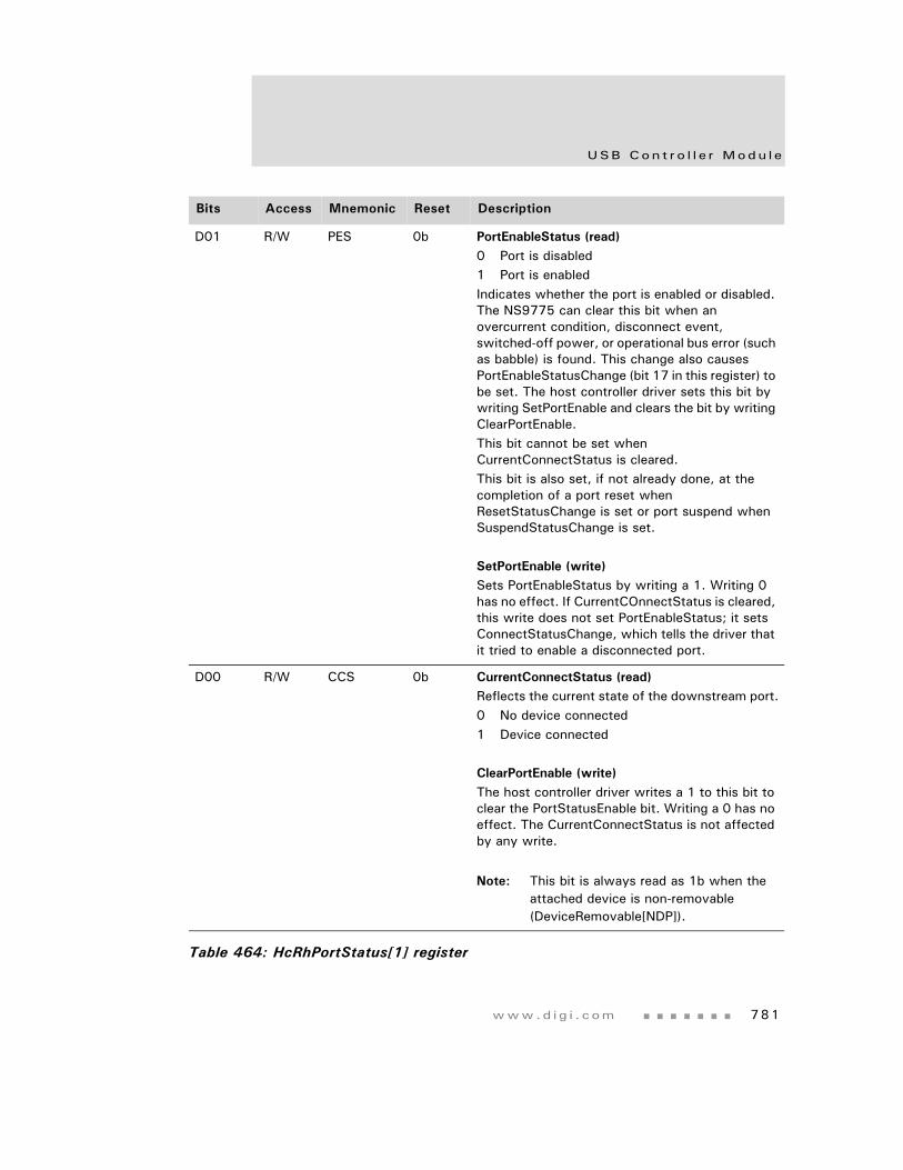
www.d i g i . com 781
USB Con t r o l l e r Modu l e
D01 R/W PES 0b PortEnableStatus (read)0 Port is disabled1 Port is enabledIndicates whether the port is enabled or disabled. The NS9775 can clear this bit when an overcurrent condition, disconnect event, switched-off power, or operational bus error (such as babble) is found. This change also causes PortEnableStatusChange (bit 17 in this register) to be set. The host controller driver sets this bit by writing SetPortEnable and clears the bit by writing ClearPortEnable. This bit cannot be set when CurrentConnectStatus is cleared.This bit is also set, if not already done, at the completion of a port reset when ResetStatusChange is set or port suspend when SuspendStatusChange is set.
SetPortEnable (write)Sets PortEnableStatus by writing a 1. Writing 0 has no effect. If CurrentCOnnectStatus is cleared, this write does not set PortEnableStatus; it sets ConnectStatusChange, which tells the driver that it tried to enable a disconnected port.
D00 R/W CCS 0b CurrentConnectStatus (read)Reflects the current state of the downstream port.0 No device connected1 Device connected
ClearPortEnable (write)The host controller driver writes a 1 to this bit to clear the PortStatusEnable bit. Writing a 0 has no effect. The CurrentConnectStatus is not affected by any write.
Note: This bit is always read as 1b when the attached device is non-removable (DeviceRemovable[NDP]).
Bits Access Mnemonic Reset Description
Table 464: HcRhPortStatus[1] register
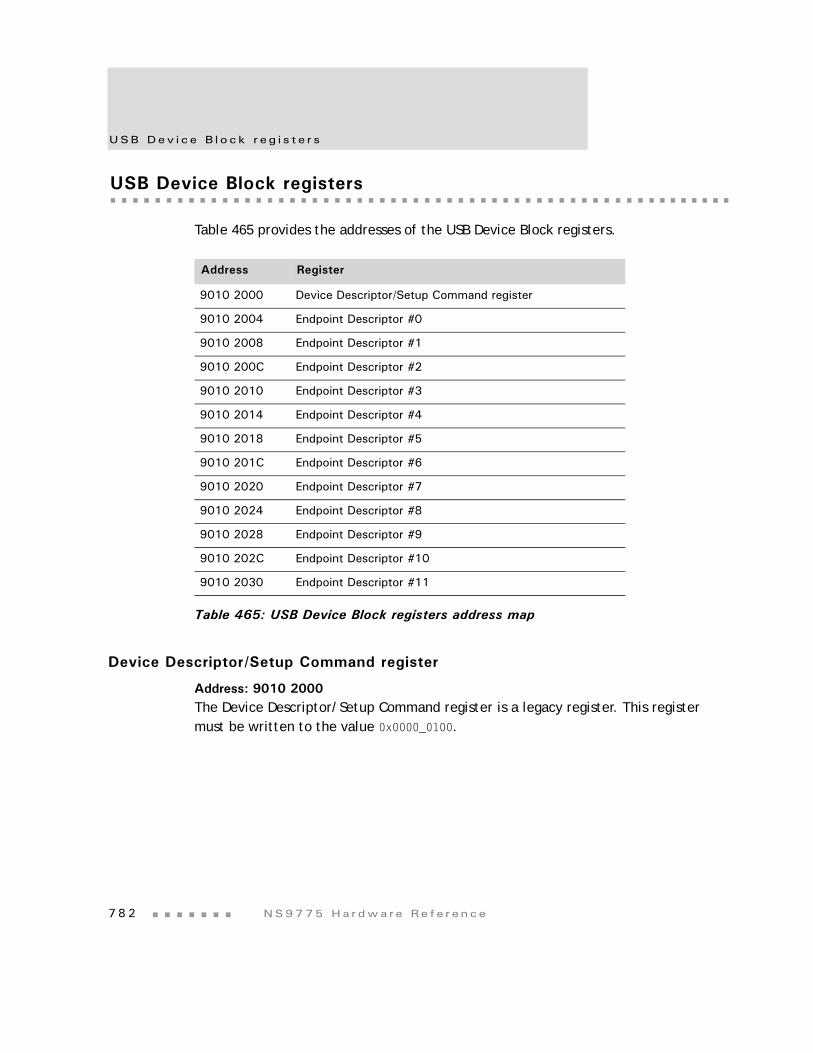
USB Dev i c e B l o ck r e g i s t e r s
7 8 2 NS9775 Ha r dwa r e Re f e r ence
USB Device Block registers
Table 465 provides the addresses of the USB Device Block registers.
Device Descriptor/Setup Command register
Address: 9010 2000The Device Descriptor/Setup Command register is a legacy register. This register must be written to the value 0x0000_0100.
Address Register
9010 2000 Device Descriptor/Setup Command register
9010 2004 Endpoint Descriptor #0
9010 2008 Endpoint Descriptor #1
9010 200C Endpoint Descriptor #2
9010 2010 Endpoint Descriptor #3
9010 2014 Endpoint Descriptor #4
9010 2018 Endpoint Descriptor #5
9010 201C Endpoint Descriptor #6
9010 2020 Endpoint Descriptor #7
9010 2024 Endpoint Descriptor #8
9010 2028 Endpoint Descriptor #9
9010 202C Endpoint Descriptor #10
9010 2030 Endpoint Descriptor #11
Table 465: USB Device Block registers address map
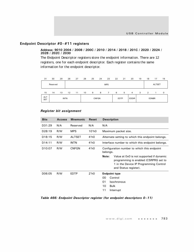
www.d i g i . com 783
USB Con t r o l l e r Modu l e
Endpoint Descriptor #0–#11 registers
Address: 9010 2004 / 2008 / 200C / 2010 / 2014 / 2018 / 201C / 2020 / 2024 / 2028 / 202C / 2030The Endpoint Descriptor registers store the endpoint information. There are 12 registers, one for each endpoint descriptor. Each register contains the same information for the endpoint descriptor.
Register bit assignment
Bits Access Mnemonic Reset Description
D31:29 N/A Reserved N/A N/A
D28:19 R/W MPS 10’h0 Maximum packet size.
D18:15 R/W ALTSET 4’h0 Alternate setting to which this endpoint belongs.
D14:11 R/W INTN 4’h0 Interface number to which this endpoint belongs.
D10:07 R/W CNFGN 4’h0 Configuration number to which this endpoint belongs.
Note: Value at 0x0 is not supported if dynamic programming is enabled (CSRPRG set to 1 in the Device IP Programming Control and Status register).
D06:05 R/W EDTP 2’h0 Endpoint type00 Control01 Isochronous10 Bulk11 Interrupt
Table 466: Endpoint Descriptor register (for endpoint descriptors 0–11)
13 12 11 10 9 8 7 6 5 4 3 2 1 015 14
31 29 28 27 26 25 24 23 22 21 20 19 18 17 1630
Reserved ALTSET
INTN
MPS
CNFGN EDDIR EDNBRALTSET EDTP
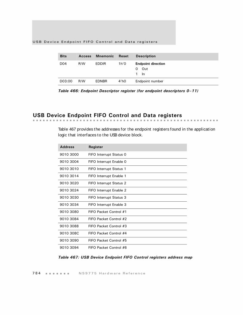
USB Dev i c e Endpo i n t F I FO Con t r o l a nd Da t a r eg i s t e r s
7 8 4 NS9775 Ha r dwa r e Re f e r ence
USB Device Endpoint FIFO Control and Data registers
Table 467 provides the addresses for the endpoint registers found in the application logic that interfaces to the USB device block.
D04 R/W EDDIR 1h’0 Endpoint direction0 Out1 In
D03:00 R/W EDNBR 4’h0 Endpoint number
Bits Access Mnemonic Reset Description
Table 466: Endpoint Descriptor register (for endpoint descriptors 0–11)
Address Register
9010 3000 FIFO Interrupt Status 0
9010 3004 FIFO Interrupt Enable 0
9010 3010 FIFO Interrupt Status 1
9010 3014 FIFO Interrupt Enable 1
9010 3020 FIFO Interrupt Status 2
9010 3024 FIFO Interrupt Enable 2
9010 3030 FIFO Interrupt Status 3
9010 3034 FIFO Interrupt Enable 3
9010 3080 FIFO Packet Control #1
9010 3084 FIFO Packet Control #2
9010 3088 FIFO Packet Control #3
9010 308C FIFO Packet Control #4
9010 3090 FIFO Packet Control #5
9010 3094 FIFO Packet Control #6
Table 467: USB Device Endpoint FIFO Control registers address map
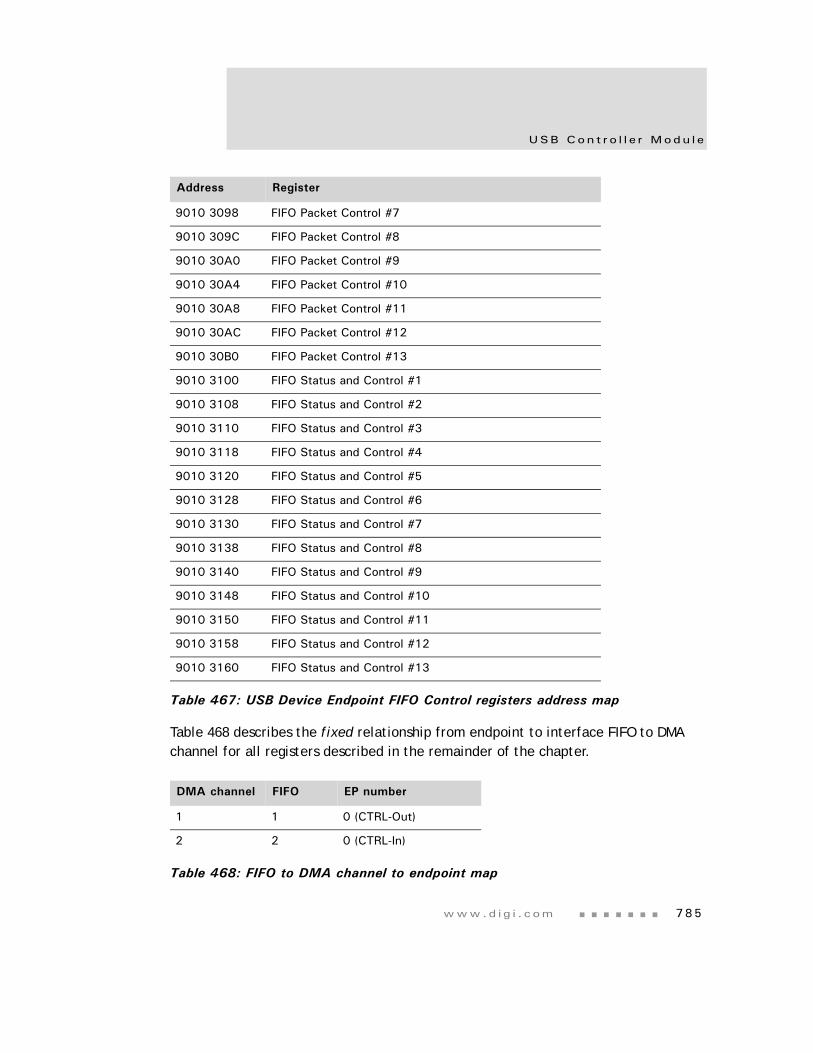
www.d i g i . com 785
USB Con t r o l l e r Modu l e
Table 468 describes the fixed relationship from endpoint to interface FIFO to DMA channel for all registers described in the remainder of the chapter.
9010 3098 FIFO Packet Control #7
9010 309C FIFO Packet Control #8
9010 30A0 FIFO Packet Control #9
9010 30A4 FIFO Packet Control #10
9010 30A8 FIFO Packet Control #11
9010 30AC FIFO Packet Control #12
9010 30B0 FIFO Packet Control #13
9010 3100 FIFO Status and Control #1
9010 3108 FIFO Status and Control #2
9010 3110 FIFO Status and Control #3
9010 3118 FIFO Status and Control #4
9010 3120 FIFO Status and Control #5
9010 3128 FIFO Status and Control #6
9010 3130 FIFO Status and Control #7
9010 3138 FIFO Status and Control #8
9010 3140 FIFO Status and Control #9
9010 3148 FIFO Status and Control #10
9010 3150 FIFO Status and Control #11
9010 3158 FIFO Status and Control #12
9010 3160 FIFO Status and Control #13
DMA channel FIFO EP number
1 1 0 (CTRL-Out)
2 2 0 (CTRL-In)
Table 468: FIFO to DMA channel to endpoint map
Address Register
Table 467: USB Device Endpoint FIFO Control registers address map
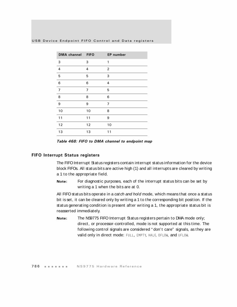
USB Dev i c e Endpo i n t F I FO Con t r o l a nd Da t a r eg i s t e r s
7 8 6 NS9775 Ha r dwa r e Re f e r ence
FIFO Interrupt Status registers
The FIFO Interrupt Status registers contain interrupt status information for the device block FIFOs. All status bits are active high (1) and all interrupts are cleared by writing a 1 to the appropriate field.
Note: For diagnostic purposes, each of the interrupt status bits can be set by writing a 1 when the bits are at 0.
All FIFO status bits operate in a catch and hold mode, which means that once a status bit is set, it can be cleared only by writing a 1 to the corresponding bit position. If the status generating condition is present after writing a 1, the appropriate status bit is reasserted immediately.
Note: The NS9775 FIFO Interrupt Status registers pertain to DMA mode only; direct, or processor-controlled, mode is not supported at this time. The following control signals are considered “don’t care” signals, as they are valid only in direct mode: FULL, EMPTY, HALF, OFLOW, and UFLOW.
3 3 1
4 4 2
5 5 3
6 6 4
7 7 5
8 8 6
9 9 7
10 10 8
11 11 9
12 12 10
13 13 11
DMA channel FIFO EP number
Table 468: FIFO to DMA channel to endpoint map
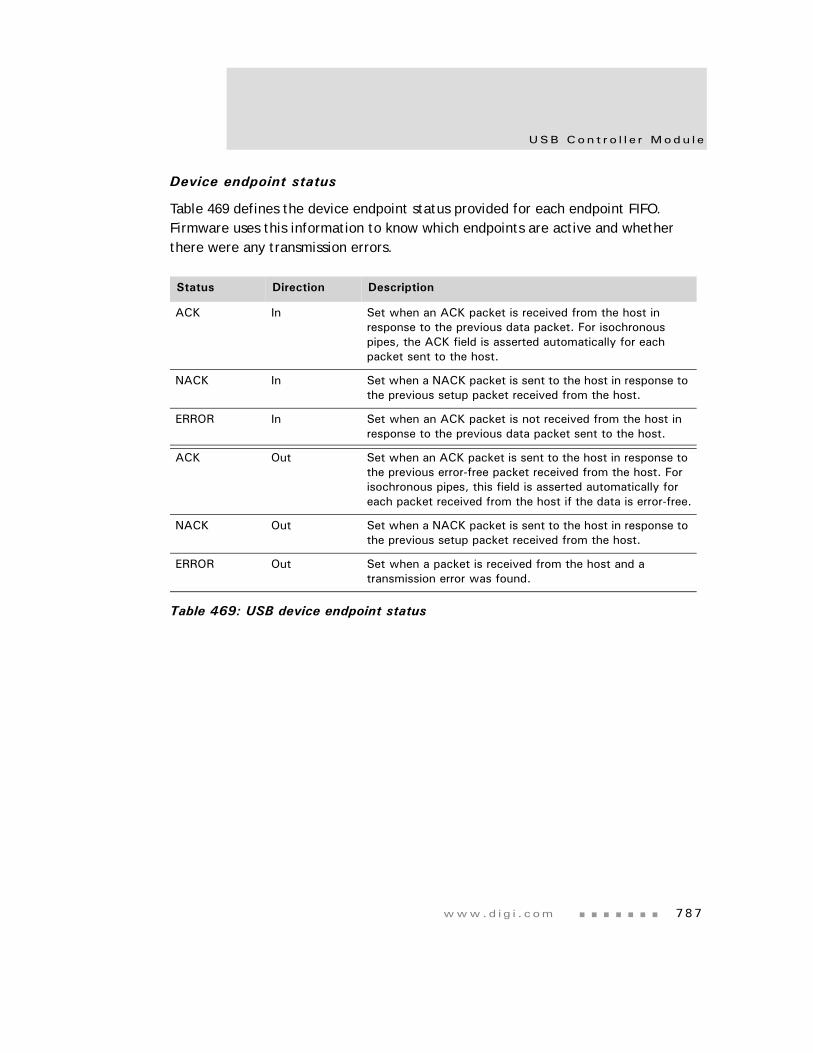
www.d i g i . com 787
USB Con t r o l l e r Modu l e
Device endpoint status
Table 469 defines the device endpoint status provided for each endpoint FIFO. Firmware uses this information to know which endpoints are active and whether there were any transmission errors.
Status Direction Description
ACK In Set when an ACK packet is received from the host in response to the previous data packet. For isochronous pipes, the ACK field is asserted automatically for each packet sent to the host.
NACK In Set when a NACK packet is sent to the host in response to the previous setup packet received from the host.
ERROR In Set when an ACK packet is not received from the host in response to the previous data packet sent to the host.
ACK Out Set when an ACK packet is sent to the host in response to the previous error-free packet received from the host. For isochronous pipes, this field is asserted automatically for each packet received from the host if the data is error-free.
NACK Out Set when a NACK packet is sent to the host in response to the previous setup packet received from the host.
ERROR Out Set when a packet is received from the host and a transmission error was found.
Table 469: USB device endpoint status
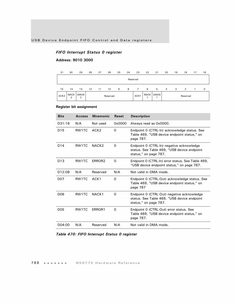
USB Dev i c e Endpo i n t F I FO Con t r o l a nd Da t a r eg i s t e r s
7 8 8 NS9775 Ha r dwa r e Re f e r ence
FIFO Interrupt Status 0 register
Address: 9010 3000
Register bit assignment
Bits Access Mnemonic Reset Description
D31:16 N/A Not used 0x0000 Always read as 0x0000.
D15 RW1TC ACK2 0 Endpoint 0 (CTRL-In) acknowledge status. See Table 469, “USB device endpoint status,” on page 787.
D14 RW1TC NACK2 0 Endpoint 0 (CTRL-In) negative acknowledge status. See Table 469, “USB device endpoint status,” on page 787.
D13 RW1TC ERROR2 0 Endpoint 0 (CTRL-In) error status. See Table 469, “USB device endpoint status,” on page 787.
D12:08 N/A Reserved N/A Not valid in DMA mode.
D07 RW1TC ACK1 0 Endpoint 0 (CTRL-Out) acknowledge status. See Table 469, “USB device endpoint status,” on page 787
D06 RW1TC NACK1 0 Endpoint 0 (CTRL-Out) negative acknowledge status. See Table 469, “USB device endpoint status,” on page 787.
D05 RW1TC ERROR1 0 Endpoint 0 (CTRL-Out) error status. See Table 469, “USB device endpoint status,” on page 787.
D04:00 N/A Reserved N/A Not valid in DMA mode.
Table 470: FIFO Interrupt Status 0 register
13 12 11 10 9 8 7 6 5 4 3 2 1 015 14
31 29 28 27 26 25 24 23 22 21 20 19 18 17 1630
Reserved
ERROR2 ReservedACK2 NACK
2 Reserved ACK1 NACK1
ERROR1
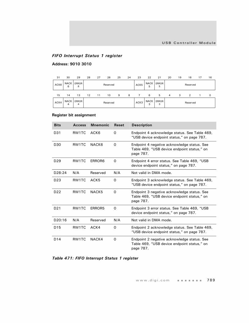
www.d i g i . com 789
USB Con t r o l l e r Modu l e
FIFO Interrupt Status 1 register
Address: 9010 3010
Register bit assignment
Bits Access Mnemonic Reset Description
D31 RW1TC ACK6 0 Endpoint 4 acknowledge status. See Table 469, “USB device endpoint status,” on page 787.
D30 RW1TC NACK6 0 Endpoint 4 negative acknowledge status. See Table 469, “USB device endpoint status,” on page 787.
D29 RW1TC ERROR6 0 Endpoint 4 error status. See Table 469, “USB device endpoint status,” on page 787.
D28:24 N/A Reserved N/A Not valid in DMA mode.
D23 RW1TC ACK5 0 Endpoint 3 acknowledge status. See Table 469, “USB device endpoint status,” on page 787.
D22 RW1TC NACK5 0 Endpoint 3 negative acknowledge status. See Table 469, “USB device endpoint status,” on page 787.
D21 RW1TC ERROR5 0 Endpoint 3 error status. See Table 469, “USB device endpoint status,” on page 787.
D20:16 N/A Reserved N/A Not valid in DMA mode.
D15 RW1TC ACK4 0 Endpoint 2 acknowledge status. See Table 469, “USB device endpoint status,” on page 787.
D14 RW1TC NACK4 0 Endpoint 2 negative acknowledge status. See Table 469, “USB device endpoint status,” on page 787.
Table 471: FIFO Interrupt Status 1 register
13 12 11 10 9 8 7 6 5 4 3 2 1 015 14
31 29 28 27 26 25 24 23 22 21 20 19 18 17 1630
Reserved
ERROR4 ReservedACK4 NACK
4 Reserved ACK3 NACK3
ERROR3
ACK6 NACK6
ERROR6
ERROR5
NACK5ACK5 Reserved
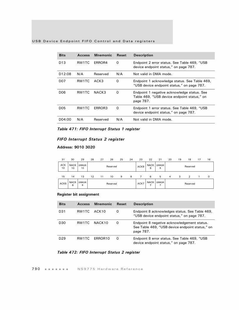
USB Dev i c e Endpo i n t F I FO Con t r o l a nd Da t a r eg i s t e r s
7 9 0 NS9775 Ha r dwa r e Re f e r ence
FIFO Interrupt Status 2 register
Address: 9010 3020
Register bit assignment
D13 RW1TC ERROR4 0 Endpoint 2 error status. See Table 469, “USB device endpoint status,” on page 787.
D12:08 N/A Reserved N/A Not valid in DMA mode.
D07 RW1TC ACK3 0 Endpoint 1 acknowledge status. See Table 469, “USB device endpoint status,” on page 787.
D06 RW1TC NACK3 0 Endpoint 1 negative acknowledge status. See Table 469, “USB device endpoint status,” on page 787.
D05 RW1TC ERROR3 0 Endpoint 1 error status. See Table 469, “USB device endpoint status,” on page 787.
D04:00 N/A Reserved N/A Not valid in DMA mode.
Bits Access Mnemonic Reset Description
D31 RW1TC ACK10 0 Endpoint 8 acknowledges status. See Table 469, “USB device endpoint status,” on page 787.
D30 RW1TC NACK10 0 Endpoint 8 negative acknowledgement status. See Table 469, “USB device endpoint status,” on page 787.
D29 RW1TC ERROR10 0 Endpoint 8 error status. See Table 469, “USB device endpoint status,” on page 787.
Table 472: FIFO Interrupt Status 2 register
Bits Access Mnemonic Reset Description
Table 471: FIFO Interrupt Status 1 register
13 12 11 10 9 8 7 6 5 4 3 2 1 015 14
31 29 28 27 26 25 24 23 22 21 20 19 18 17 1630
Reserved
ERROR8 ReservedACK8 NACK
8 Reserved ACK7 NACK7
ERROR7
ACK10
NACK10
ERROR10
ERROR9
NACK9ACK9 Reserved
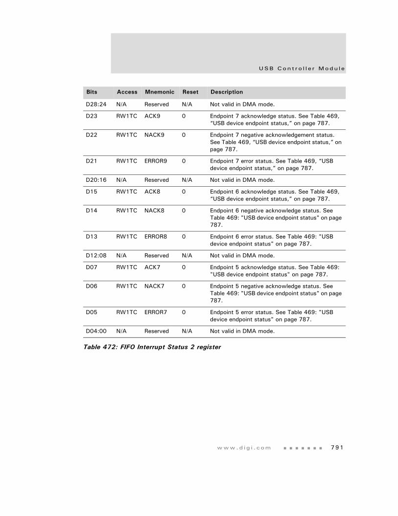
www.d i g i . com 791
USB Con t r o l l e r Modu l e
D28:24 N/A Reserved N/A Not valid in DMA mode.
D23 RW1TC ACK9 0 Endpoint 7 acknowledge status. See Table 469, “USB device endpoint status,” on page 787.
D22 RW1TC NACK9 0 Endpoint 7 negative acknowledgement status. See Table 469, “USB device endpoint status,” on page 787.
D21 RW1TC ERROR9 0 Endpoint 7 error status. See Table 469, “USB device endpoint status,” on page 787.
D20:16 N/A Reserved N/A Not valid in DMA mode.
D15 RW1TC ACK8 0 Endpoint 6 acknowledge status. See Table 469, “USB device endpoint status,” on page 787.
D14 RW1TC NACK8 0 Endpoint 6 negative acknowledge status. See Table 469: "USB device endpoint status" on page 787.
D13 RW1TC ERROR8 0 Endpoint 6 error status. See Table 469: "USB device endpoint status" on page 787.
D12:08 N/A Reserved N/A Not valid in DMA mode.
D07 RW1TC ACK7 0 Endpoint 5 acknowledge status. See Table 469: "USB device endpoint status" on page 787.
D06 RW1TC NACK7 0 Endpoint 5 negative acknowledge status. See Table 469: "USB device endpoint status" on page 787.
D05 RW1TC ERROR7 0 Endpoint 5 error status. See Table 469: "USB device endpoint status" on page 787.
D04:00 N/A Reserved N/A Not valid in DMA mode.
Bits Access Mnemonic Reset Description
Table 472: FIFO Interrupt Status 2 register
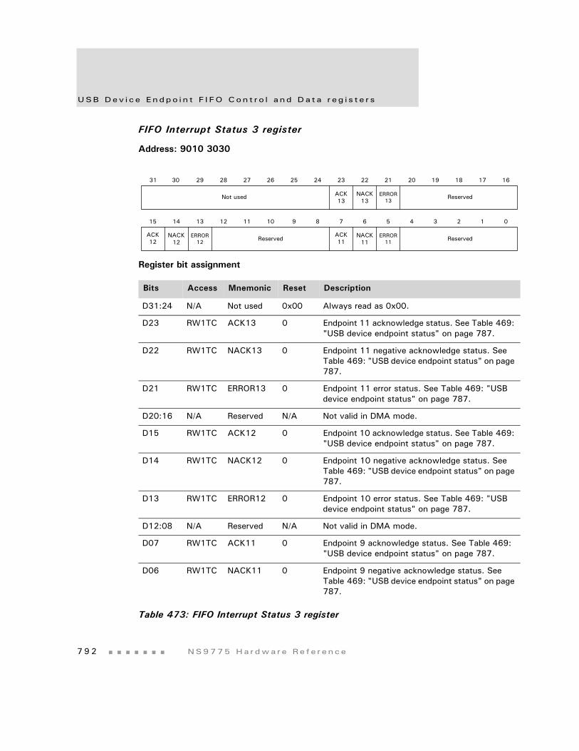
USB Dev i c e Endpo i n t F I FO Con t r o l a nd Da t a r eg i s t e r s
7 9 2 NS9775 Ha r dwa r e Re f e r ence
FIFO Interrupt Status 3 register
Address: 9010 3030
Register bit assignment
Bits Access Mnemonic Reset Description
D31:24 N/A Not used 0x00 Always read as 0x00.
D23 RW1TC ACK13 0 Endpoint 11 acknowledge status. See Table 469: "USB device endpoint status" on page 787.
D22 RW1TC NACK13 0 Endpoint 11 negative acknowledge status. See Table 469: "USB device endpoint status" on page 787.
D21 RW1TC ERROR13 0 Endpoint 11 error status. See Table 469: "USB device endpoint status" on page 787.
D20:16 N/A Reserved N/A Not valid in DMA mode.
D15 RW1TC ACK12 0 Endpoint 10 acknowledge status. See Table 469: "USB device endpoint status" on page 787.
D14 RW1TC NACK12 0 Endpoint 10 negative acknowledge status. See Table 469: "USB device endpoint status" on page 787.
D13 RW1TC ERROR12 0 Endpoint 10 error status. See Table 469: "USB device endpoint status" on page 787.
D12:08 N/A Reserved N/A Not valid in DMA mode.
D07 RW1TC ACK11 0 Endpoint 9 acknowledge status. See Table 469: "USB device endpoint status" on page 787.
D06 RW1TC NACK11 0 Endpoint 9 negative acknowledge status. See Table 469: "USB device endpoint status" on page 787.
Table 473: FIFO Interrupt Status 3 register
13 12 11 10 9 8 7 6 5 4 3 2 1 015 14
31 29 28 27 26 25 24 23 22 21 20 19 18 17 1630
Not used
ERROR12 Reserved
ACK12
NACK12 Reserved
ACK11
NACK11
ERROR11
ERROR13
NACK13
ACK13
Reserved
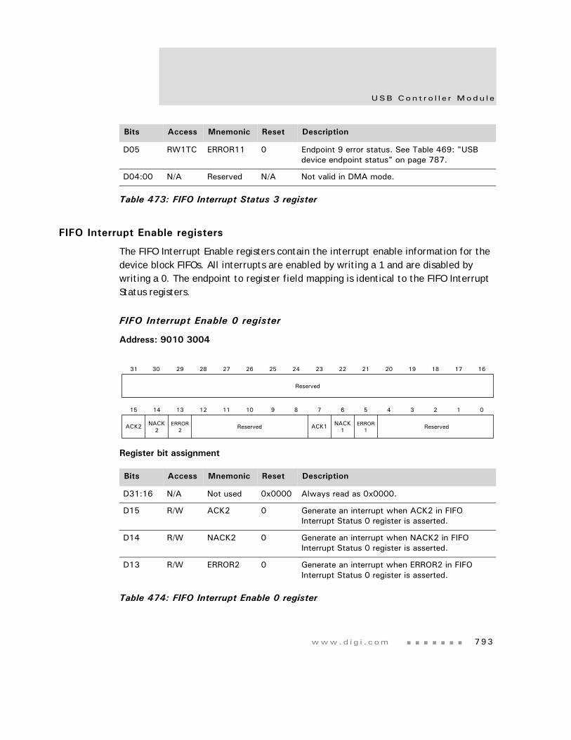
www.d i g i . com 793
USB Con t r o l l e r Modu l e
FIFO Interrupt Enable registers
The FIFO Interrupt Enable registers contain the interrupt enable information for the device block FIFOs. All interrupts are enabled by writing a 1 and are disabled by writing a 0. The endpoint to register field mapping is identical to the FIFO Interrupt Status registers.
FIFO Interrupt Enable 0 register
Address: 9010 3004
Register bit assignment
D05 RW1TC ERROR11 0 Endpoint 9 error status. See Table 469: "USB device endpoint status" on page 787.
D04:00 N/A Reserved N/A Not valid in DMA mode.
Bits Access Mnemonic Reset Description
Table 473: FIFO Interrupt Status 3 register
Bits Access Mnemonic Reset Description
D31:16 N/A Not used 0x0000 Always read as 0x0000.
D15 R/W ACK2 0 Generate an interrupt when ACK2 in FIFO Interrupt Status 0 register is asserted.
D14 R/W NACK2 0 Generate an interrupt when NACK2 in FIFO Interrupt Status 0 register is asserted.
D13 R/W ERROR2 0 Generate an interrupt when ERROR2 in FIFO Interrupt Status 0 register is asserted.
Table 474: FIFO Interrupt Enable 0 register
13 12 11 10 9 8 7 6 5 4 3 2 1 015 14
31 29 28 27 26 25 24 23 22 21 20 19 18 17 1630
Reserved
ERROR2 ReservedACK2 NACK
2 Reserved ACK1 NACK1
ERROR1
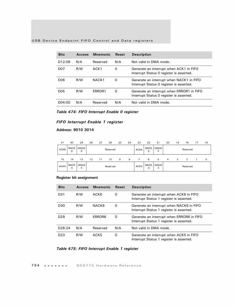
USB Dev i c e Endpo i n t F I FO Con t r o l a nd Da t a r eg i s t e r s
7 9 4 NS9775 Ha r dwa r e Re f e r ence
FIFO Interrupt Enable 1 register
Address: 9010 3014
Register bit assignment
D12:08 N/A Reserved N/A Not valid in DMA mode.
D07 R/W ACK1 0 Generate an interrupt when ACK1 in FIFO Interrupt Status 0 register is asserted.
D06 R/W NACK1 0 Generate an interrupt when NACK1 in FIFO Interrupt Status 0 register is asserted.
D05 R/W ERROR1 0 Generate an interrupt when ERROR1 in FIFO Interrupt Status 0 register is asserted.
D04:00 N/A Reserved N/A Not valid in DMA mode.
Bits Access Mnemonic Reset Description
D31 R/W ACK6 0 Generate an interrupt when ACK6 in FIFO Interrupt Status 1 register is asserted.
D30 R/W NACK6 0 Generate an interrupt when NACK6 in FIFO Interrupt Status 1 register is asserted.
D29 R/W ERROR6 0 Generate an interrupt when ERROR6 in FIFO Interrupt Status 1 register is asserted.
D28:24 N/A Reserved N/A Not valid in DMA mode.
D23 R/W ACK5 0 Generate an interrupt when ACK5 in FIFO Interrupt Status 1 register is asserted.
Table 475: FIFO Interrupt Enable 1 register
Bits Access Mnemonic Reset Description
Table 474: FIFO Interrupt Enable 0 register
13 12 11 10 9 8 7 6 5 4 3 2 1 015 14
31 29 28 27 26 25 24 23 22 21 20 19 18 17 1630
Reserved
ERROR4 ReservedACK4 NACK
4 Reserved ACK3 NACK3
ERROR3
ACK6 NACK6
ERROR6
ERROR5
NACK5ACK5 Reserved
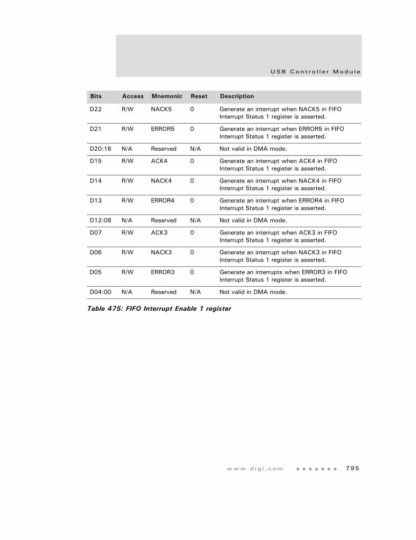
www.d i g i . com 795
USB Con t r o l l e r Modu l e
D22 R/W NACK5 0 Generate an interrupt when NACK5 in FIFO Interrupt Status 1 register is asserted.
D21 R/W ERROR5 0 Generate an interrupt when ERROR5 in FIFO Interrupt Status 1 register is asserted.
D20:16 N/A Reserved N/A Not valid in DMA mode.
D15 R/W ACK4 0 Generate an interrupt when ACK4 in FIFO Interrupt Status 1 register is asserted.
D14 R/W NACK4 0 Generate an interrupt when NACK4 in FIFO Interrupt Status 1 register is asserted.
D13 R/W ERROR4 0 Generate an interrupt when ERROR4 in FIFO Interrupt Status 1 register is asserted.
D12:08 N/A Reserved N/A Not valid in DMA mode.
D07 R/W ACK3 0 Generate an interrupt when ACK3 in FIFO Interrupt Status 1 register is asserted.
D06 R/W NACK3 0 Generate an interrupt when NACK3 in FIFO Interrupt Status 1 register is asserted.
D05 R/W ERROR3 0 Generate an interrupts when ERROR3 in FIFO Interrupt Status 1 register is asserted.
D04:00 N/A Reserved N/A Not valid in DMA mode.
Bits Access Mnemonic Reset Description
Table 475: FIFO Interrupt Enable 1 register
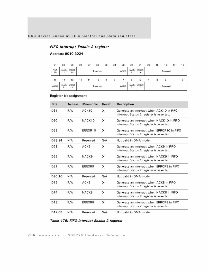
USB Dev i c e Endpo i n t F I FO Con t r o l a nd Da t a r eg i s t e r s
7 9 6 NS9775 Ha r dwa r e Re f e r ence
FIFO Interrupt Enable 2 register
Address: 9010 3024
Register bit assignment
Bits Access Mnemonic Reset Description
D31 R/W ACK10 0 Generate an interrupt when ACK10 in FIFO Interrupt Status 2 register is asserted,
D30 R/W NACK10 0 Generate an interrupt when NACK10 in FIFO Interrupt Status 2 register is asserted.
D29 R/W ERROR10 0 Generate an interrupt when ERROR10 in FIFO Interrupt Status 2 register is asserted.
D28:24 N/A Reserved N/A Not valid in DMA mode.
D23 R/W ACK9 0 Generate an interrupt when ACK9 in FIFO Interrupt Status 2 register is asserted.
D22 R/W NACK9 0 Generate an interrupt when NACK9 in FIFO Interrupt Status 2 register is asserted.
D21 R/W ERROR9 0 Generate an interrupt when ERROR9 in FIFO Interrupt Status 2 register is asserted.
D20:16 N/A Reserved N/A Not valid in DMA mode.
D15 R/W ACK8 0 Generate an interrupt when ACK8 in FIFO Interrupt Status 2 register is asserted.
D14 R/W NACK8 0 Generate an interrupt when NACK8 in FIFO Interrupt Status 2 register is asserted.
D13 R/W ERROR8 0 Generate an interrupt when ERROR8 in FIFO Interrupt Status 2 register is asserted.
D12:08 N/A Reserved N/A Not valid in DMA mode.
Table 476: FIFO Interrupt Enable 2 register
13 12 11 10 9 8 7 6 5 4 3 2 1 015 14
31 29 28 27 26 25 24 23 22 21 20 19 18 17 1630
Reserved
ERROR8 ReservedACK8 NACK
8 Reserved ACK7 NACK7
ERROR7
ACK10
NACK10
ERROR10
ERROR9
NACK9ACK9 Reserved
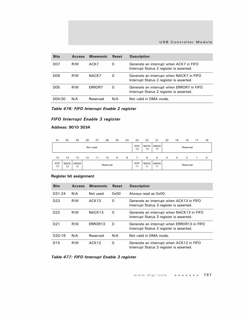
www.d i g i . com 797
USB Con t r o l l e r Modu l e
FIFO Interrupt Enable 3 register
Address: 9010 3034
Register bit assignment
D07 R/W ACK7 0 Generate an interrupt when ACK7 in FIFO Interrupt Status 2 register is asserted.
D06 R/W NACK7 0 Generate an interrupt when NACK7 in FIFO Interrupt Status 2 register is asserted.
D05 R/W ERROR7 0 Generate an interrupt when ERROR7 in FIFO Interrupt Status 2 register is asserted.
D04:00 N/A Reserved N/A Not valid in DMA mode.
Bits Access Mnemonic Reset Description
D31:24 N/A Not used 0x00 Always read as 0x00.
D23 R/W ACK13 0 Generate an interrupt when ACK13 in FIFO Interrupt Status 3 register is asserted.
D22 R/W NACK13 0 Generate an interrupt when NACK13 in FIFO Interrupt Status 3 register is asserted.
D21 R/W ERROR13 0 Generate an interrupt when ERROR13 in FIFO Interrupt Status 3 register is asserted.
D20:16 N/A Reserved N/A Not valid in DMA mode.
D15 R/W ACK12 0 Generate an interrupt when ACK12 in FIFO Interrupt Status 3 register is asserted.
Table 477: FIFO Interrupt Enable 3 register
Bits Access Mnemonic Reset Description
Table 476: FIFO Interrupt Enable 2 register
13 12 11 10 9 8 7 6 5 4 3 2 1 015 14
31 29 28 27 26 25 24 23 22 21 20 19 18 17 1630
Not used
ERROR12 Reserved
ACK12
NACK12 Reserved
ACK11
NACK11
ERROR11
ERROR13
NACK13
ACK13
Reserved
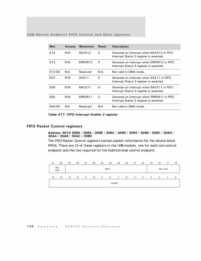
USB Dev i c e Endpo i n t F I FO Con t r o l a nd Da t a r eg i s t e r s
7 9 8 NS9775 Ha r dwa r e Re f e r ence
FIFO Packet Control registers
Address: 9010 3080 / 3084 / 3088 / 308C / 3090 / 3094 / 3098 / 309C / 30A0 / 30A4 / 30A8 / 30AC / 30B0The FIFO Packet Control registers contain packet information for the device block FIFOs. There are 13 of these registers in the USB module, one for each non-control endpoint and the two required for the bidirectional control endpoint.
D14 R/W NACK12 0 Generate an interrupt when NACK12 in FIFO Interrupt Status 3 register is asserted.
D13 R/W ERROR12 0 Generate an interrupt when ERROR12 in FIFO Interrupt Status 3 register is asserted.
D12:08 N/A Reserved N/A Not valid in DMA mode.
D07 R/W ACK11 0 Generate an interrupt when ACK11 in FIFO Interrupt Status 3 register is asserted,
D06 R/W NACK11 0 Generate an interrupt when NACK11 in FIFO Interrupt Status 3 register is asserted.
D05 R/W ERROR11 0 Generate an interrupt when ERROR11 in FIFO Interrupt Status 3 register is asserted.
D04:00 N/A Reserved N/A Not valid in DMA mode.
Bits Access Mnemonic Reset Description
Table 477: FIFO Interrupt Enable 3 register
13 12 11 10 9 8 7 6 5 4 3 2 1 015 14
31 29 28 27 26 25 24 23 22 21 20 19 18 17 1630
MAX
COUNT
Notused Not used
www.d i g i . com 799
USB Con t r o l l e r Modu l e
Register bit assignment
FIFO Status and Control registers
Address: 9010 3100 / 3108 / 3110 / 3118 / 3120 / 3128 / 3130 / 3138 / 3140 / 3148 / 3150 / 3158 / 3160The FIFO Status and Control registers contain additional status and control information for the device block FIFOs. There are 13 of these registers in the USB module, one for each non-control endpoint and the two required for the bidirectional endpoint.
Bits Access Mnemonic Reset Description
D31:30 N/A Not used 0x0 Always read as 0x0.
D29:20 R/W MAX 0x040 Indicates the maximum packet size supported by the associated USB device endpoint. This value should be set to the same value as the maximum packet size (see page 783) in the Endpoint Descriptor register.
Note: This field does not apply for FIFO #2 as that FIFO is dedicated to the IN direction of the control endpoint.
D19:16 N/A Not used 0x00 Always read as 0x00.
D15:00 R COUNT 0x0000 Indicates the number of error-free packets sent by the USB device module (USB-IN transactions) with the current DMA buffer descriptor for the associated FIFO.
Note: This field does not apply for FIFO #1 as that FIFO is dedicated to the OUT direction of the control endpoint.
Table 478: FIFO Packet Control registers
M31 M30 CIA
13 12 11 10 9 8 7 6 5 4 3 2 1 015 14
STATE
31 29 28 27 26 25 24 23 22 21 20 19 18 17 1630
Reserved TYPE CLR DIR FDBNot used
USB Dev i c e Endpo i n t F I FO Con t r o l a nd Da t a r eg i s t e r s
8 0 0 NS9775 Ha r dwa r e Re f e r ence
Register bit assignment
Bits Access Mnemonic Reset Description
D31:24 N/A Reserved N/A N/A
D23:22 R/W Not used 0x0 Always write as 00.
D21:20 R/W TYPE 0x0 Type fieldDefines the endpoint type associated with the FIFO. 00 Control01 Isochronous10 Bulk11 Interrupt
D19 R/W CLR 1 Clear fieldWriting a 1 places the FIFO into the reset state, disabling the associated endpoint. Any data currently in the FIFO is flushed. When the endpoint is configured for the IN direction and the type is either bulk or interrupt, this bit is also set to 1 by the hardware when a packet error is found by the host.
D18 R/W DIR 0 Direction field0 Defines the OUT direction1 Defines the IN directionDefines the FIFO (endpoint) direction.
D17:16 R FDB 0x0 Valid data bytesIndicates the valid number of bytes in the FIFO when receiving; this field is always 0 when transmitting.
Note: This field is not used when using the DMA controller.
Table 479: FIFO Status and Control registers
www.d i g i . com 801
USB Con t r o l l e r Modu l e
D15:14 R STATE 0x0 State fieldDefines the state of the endpoint after the most recent communication with the USB device module. 00 Undefined01 Data phase transaction10 Status phase transaction11 No-data status phase transactionThis field is used primarily for diagnostic purposes.
D13 R M31 0 Successful transfer status bit0 Unsuccessful transfer1 Successful transferFor successful transfers
For IN packets: If the host sends an ACK handshake (when the command involves a handshake), this bit is set, indicating that the data is transferred successfully to the host.
For OUT and SETUP packets: When set, this bit also indicates that an ACK handshake is being sent to the host.
For unsuccessful transfers
For OUT packets with errors, this bit is cleared.
For IN packets, this bit is cleared if an ACK handshake was not sent.
When cleared for IN and OUT packets, this bit also indicates a timeout or NAK/STALL handshake is being sent to the host.
D12 R M30 0 Setup command status bit0 Current transaction is not a setup command1 Current transaction is a setup command
Bits Access Mnemonic Reset Description
Table 479: FIFO Status and Control registers
USB Dev i c e Endpo i n t F I FO Con t r o l a nd Da t a r eg i s t e r s
8 0 2 NS9775 Ha r dwa r e Re f e r ence
D11:00 R CIA 0x000 Configuration Interface AlternateValue depends on setting of the M30 field (D12 in this register).
If M30 = 1, this field contains the value 0x100.
If the M30 = 0, this field contains the following:
[11:08] — configuration
[07:04] — interface
[03:00] — alternate
Bits Access Mnemonic Reset Description
Table 479: FIFO Status and Control registers
803
TimingC H A P T E R 1 7
This chapter provides the electrical specifications, or timing, integral to the operation of the NS9775. Timing includes information about DC and AC characteristics, output rise and fall timing, and crystal oscillator specifications.
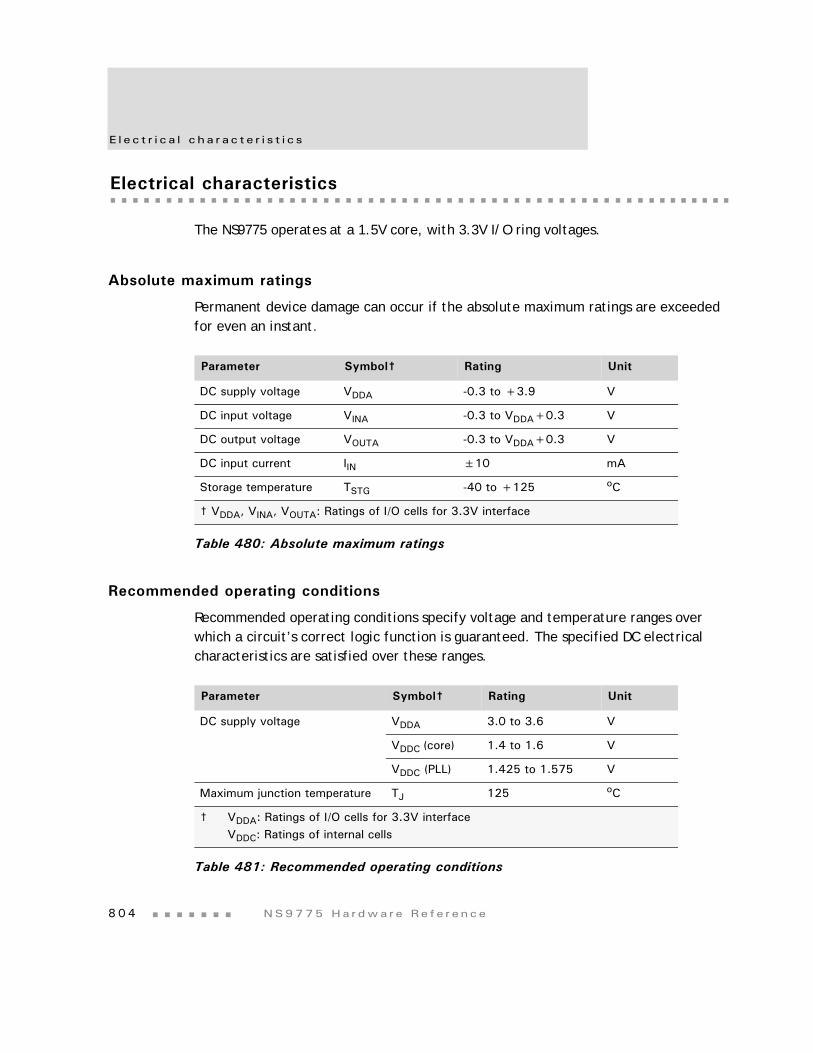
E l e c t r i c a l c ha r ac t e r i s t i c s
8 0 4 NS9775 Ha r dwa r e Re f e r ence
Electrical characteristics
The NS9775 operates at a 1.5V core, with 3.3V I/O ring voltages.
Absolute maximum ratings
Permanent device damage can occur if the absolute maximum ratings are exceeded for even an instant.
Recommended operating conditions
Recommended operating conditions specify voltage and temperature ranges over which a circuit’s correct logic function is guaranteed. The specified DC electrical characteristics are satisfied over these ranges.
Parameter Symbol† Rating Unit
DC supply voltage VDDA -0.3 to +3.9 V
DC input voltage VINA -0.3 to VDDA+0.3 V
DC output voltage VOUTA -0.3 to VDDA+0.3 V
DC input current IIN ±10 mA
Storage temperature TSTG -40 to +125 oC
† VDDA, VINA, VOUTA: Ratings of I/O cells for 3.3V interface
Table 480: Absolute maximum ratings
Parameter Symbol† Rating Unit
DC supply voltage VDDA 3.0 to 3.6 V
VDDC (core) 1.4 to 1.6 V
VDDC (PLL) 1.425 to 1.575 V
Maximum junction temperature TJ 125 oC
† VDDA: Ratings of I/O cells for 3.3V interfaceVDDC: Ratings of internal cells
Table 481: Recommended operating conditions
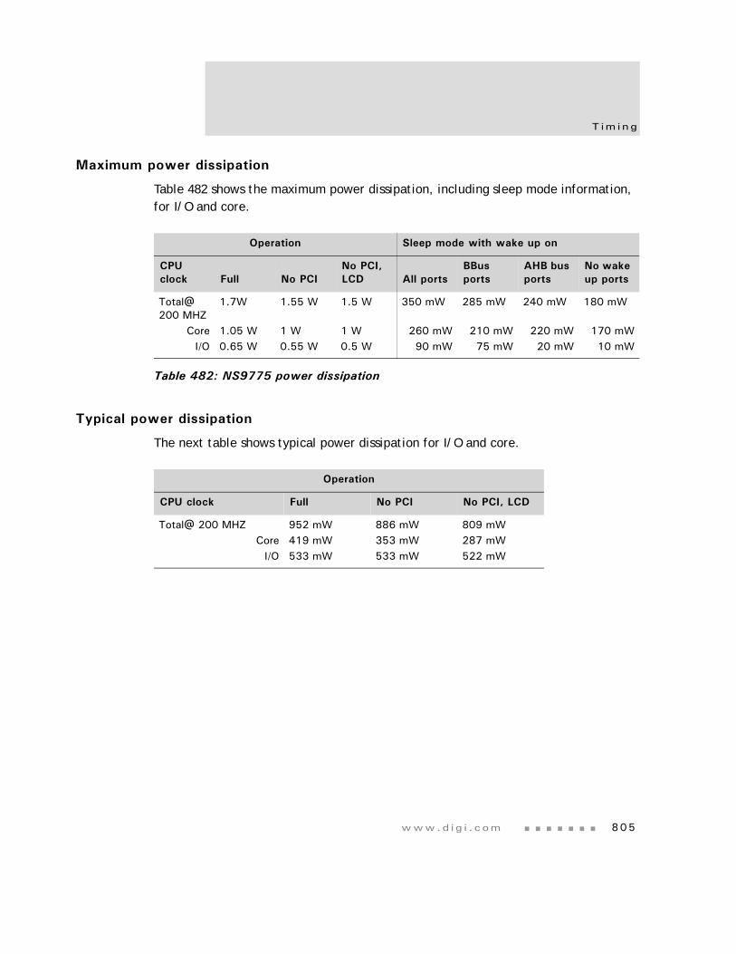
www.d i g i . com 805
T im i ng
Maximum power dissipation
Table 482 shows the maximum power dissipation, including sleep mode information, for I/O and core.
Typical power dissipation
The next table shows typical power dissipation for I/O and core.
Operation Sleep mode with wake up on
CPU clock Full No PCI
No PCI, LCD All ports
BBus ports
AHB bus ports
No wake up ports
Total@200 MHZ
CoreI/O
1.7W
1.05 W0.65 W
1.55 W
1 W0.55 W
1.5 W
1 W0.5 W
350 mW
260 mW90 mW
285 mW
210 mW75 mW
240 mW
220 mW20 mW
180 mW
170 mW10 mW
Table 482: NS9775 power dissipation
Operation
CPU clock Full No PCI No PCI, LCD
Total@ 200 MHZCore
I/O
952 mW419 mW533 mW
886 mW353 mW533 mW
809 mW287 mW522 mW
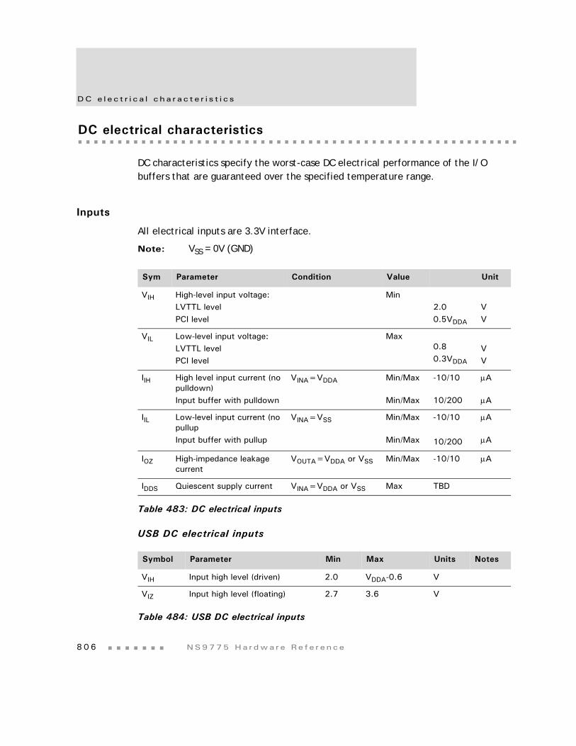
DC e l e c t r i c a l c ha r a c t e r i s t i c s
8 0 6 NS9775 Ha r dwa r e Re f e r ence
DC electrical characteristics
DC characteristics specify the worst-case DC electrical performance of the I/O buffers that are guaranteed over the specified temperature range.
Inputs
All electrical inputs are 3.3V interface.
Note: VSS = 0V (GND)
USB DC electrical inputs
Sym Parameter Condition Value Unit
VIH High-level input voltage:LVTTL levelPCI level
Min2.00.5VDDA
VV
VIL Low-level input voltage:LVTTL levelPCI level
Max0.80.3VDDA
VV
IIH High level input current (no pulldown)Input buffer with pulldown
VINA=VDDA Min/Max
Min/Max
-10/10
10/200
μA
μA
IIL Low-level input current (no pullupInput buffer with pullup
VINA=VSS Min/Max
Min/Max
-10/10
10/200
μA
μA
IOZ High-impedance leakage current
VOUTA=VDDA or VSS Min/Max -10/10 μA
IDDS Quiescent supply current VINA=VDDA or VSS Max TBD
Table 483: DC electrical inputs
Symbol Parameter Min Max Units Notes
VIH Input high level (driven) 2.0 VDDA-0.6 V
VIZ Input high level (floating) 2.7 3.6 V
Table 484: USB DC electrical inputs
www.d i g i . com 807
T im i ng
Notes:1 |(usb_dp) – (usb_dm)|
2 Includes VDI range.
Outputs
All electrical outputs are 3.3V interface.
USB DC electrical outputs
Notes:1 Measured with RL of 1.425k ohm to 3.6V.
2 Measured with RL of 14.25k ohm to GND.
3 Excluding the first transition from the idle state.
VIL Input low level 0.8 V
VDI Differential input sensitivity 0.2 V 1
VCM Differential common mode range 0.8 2.5 V 2
Symbol Parameter Min Max Units Notes
Table 484: USB DC electrical inputs
Sym Parameter Value Unit
VOH High-level output voltage (LVTTL) Min VDDA-0.6 V
VOL Low-level output voltage (LVTTL) Max 0.4 V
VOH PCI high-level output voltage Min 0.9VDDA V
VOL PCI low-level output voltage Max 0.1VDDA V
Table 485: DC electrical outputs
Symbol Parameter Min Max Units Notes
VOL Output low level 0.0 0.3 V 1
VOH Output high level 2.8 3.6 V 2
VCRS Output signal crossover voltage 1.3 2.0 V 3
Table 486: USB DC electrical outputs
Powe r s equenc i ng
8 0 8 NS9775 Ha r dwa r e Re f e r ence
Power sequencing
Use these requirements for power sequencing:
3.3 volt and 1.5 volt power must be applied to the NS9775 ASIC simultaneously, but never more than 100 milliseconds difference.
The ASIC NS9775 3.3 volt/1.5 volt supplies must maintain a relationship to the power supplies for the external board circuits such that ASIC I/O input voltage does not exceed ±0.3V before the ASIC power supplies are applied.
3.3 and 1.5 volt power should never be cycled more than 100 times per day.
www.d i g i . com 809
T im i ng
Memory timing
Note: All AC characteristics are measured with 35pF, unless otherwise noted.
Memory timing contains parameters and diagrams for both SDRAM and SRAM timing.
Table 487 describes the values shown in the SDRAM timing diagrams (Figure 107 through Figure 115).
Notes:1 All four data_mask signals are used for all transfers.
2 All four data_mask signals will go low during a read cycle, for both 16-bit and 32-bit transfers.
3 Only one of the four clk_out signals is used.
4 Only one of the four dy_cs_n signals is used.
Parm Description Min Max Unit Notes
M1 data input setup time to rising 1.6 ns
M2 data input hold time to rising 3.3 ns
M3 clk_out high to clk_en high 6.1 ns
M4 clk_out high to address valid 6.1 ns
M5 clk_out high to data_mask 6.1 ns 1, 2
M6 clk_out high to dy_cs_n low 6.1 ns 3, 4
M7 clk_out high to ras_n low 6.1 ns
M8 clk_out high to cas_n low 6.1 ns
M9 clk_out high to we_n low 6.1 ns
M10 clk_out high to data out 6.2 ns
M11 address hold time 3.5
M12 data out hold time 3.8
M13 clk_en high to sdram access 2 2 clock
M14 end sdram access to clk_en low 2 2 clock
Table 487: SDRAM timing parameters
Memo ry t im i ng
8 1 0 NS9775 Ha r dwa r e Re f e r ence
SDRAM burst read (16-bit)
Figure 107: SDRAM burst read (16-bit) timing
Notes:1 This is the bank and RAS address.
2 This is the CAS address.
pre act read lat d-A d-B d-C d-D d-E d-F d-G d-H
M9
M8
M7
M6
M5
M11M4
M2M1
Note-1 Note-2
clk_out<3:0>
data<31:16>
addr
data_mask<3:0>
dy_cs_n<3:0>*
ras_n
cas_n
we_n
www.d i g i . com 811
T im i ng
SDRAM burst read (16-bit), CAS latency = 3
Figure 108: SDRAM burst read (16-bit), CAS latency = 3 timing
Notes:1 This is the bank and RAS address.
2 This is the CAS address.
pre act read lat lat d-A d-B d-C d-D d-E d-F d-G d-H
M9
M8
M7
M6
M5
M11M4
M2M1
Note-1 Note-2
clk_out<3:0>
data<31:16>
addr
data_mask<3:0>
dy_cs_n<3:0>*
ras_n
cas_n
we_n
Memo ry t im i ng
8 1 2 NS9775 Ha r dwa r e Re f e r ence
SDRAM burst write (16-bit)
Figure 109: SDRAM burst write (16-bit) timing
Notes:1 This is the bank and RAS address.
2 This is the CAS address.
pre act wr d-A d-B d-C d-D d-E d-F d-G d-H
M9
M8
M7
M6
M5
M5
M4
M12M10
Note-1 Note-2
clk_out<3:0>
data<31:0>
addr
data_mask<3:2>
data_mask<1:0>*
dy_cs_n<3:0>*
ras_n
cas_n
we_n
www.d i g i . com 813
T im i ng
SDRAM burst read (32-bit)
Figure 110: SDRAM burst read (32-bit) timing
Notes:1 This is the bank and RAS address.
2 This is the CAS address.
prechg active read cas lat data-A data-B data-C data-D
M9
M8
M7
M6
M5
M11M4
M2M1
Note-1 Note-2
clk_out<3:0>
data<31:0>
addr
data_mask<3:0>*
dy_cs_n<3:0>*
ras_n
cas_n
we_n
Memo ry t im i ng
8 1 4 NS9775 Ha r dwa r e Re f e r ence
SDRAM burst read (32-bit), CAS latency = 3
Figure 111: SDRAM burst read (32-bit), CAS latency = 3 timing
Notes:1 This is the bank and RAS address.
2 This is the CAS address.
pre act read lat lat data-A data-B data-C data-D
M9
M8
M7
M6
M5
M11M4
M2M1
Note-1 Note-2
clk_out<3:0>
data<31:0>
addr
data_mask<3:0>*
dy_cs_n<3:0>*
ras_n
cas_n
we_n
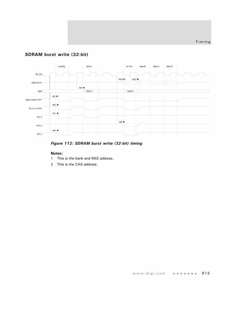
www.d i g i . com 815
T im i ng
SDRAM burst write (32-bit)
Figure 112: SDRAM burst write (32-bit) timing
Notes:1 This is the bank and RAS address.
2 This is the CAS address.
prechg active wr d-A data-B data-C data-D
M9
M8
M7
M6
M5
M4
M12M10
Note-1 Note-2
clk_out
data<31:0>
addr
data_mask<3:0>*
dy_cs_n<3:0>
ras_n
cas_n
we_n
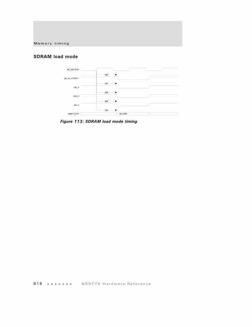
Memo ry t im i ng
8 1 6 NS9775 Ha r dwa r e Re f e r ence
SDRAM load mode
Figure 113: SDRAM load mode timing
M4
M9
M8
M7
M5
op code
clk_out<3:0>
dy_cs_n<3:0>*
ras_n
cas_n
we_n
addr<11:0>
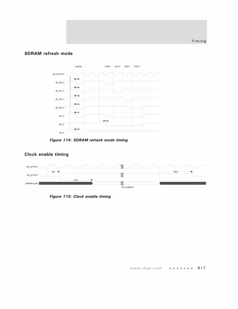
www.d i g i . com 817
T im i ng
SDRAM refresh mode
Figure 114: SDRAM refresh mode timing
Clock enable timing
Figure 115: Clock enable timing
prechg CS0 rf CS1 rf CS2 rf CS3 rf
M9
M8
M7
M6
M6
M6
M6
clk_out<3:0>
dy_cs0_n
dy_cs1_n
dy_cs2_n
dy_cs3_n
ras_n
cas_n
we_n
M13
M14M3
clk_enable.td
clk_out<3:0>
clk_en<3:0>
SDRAM cycle
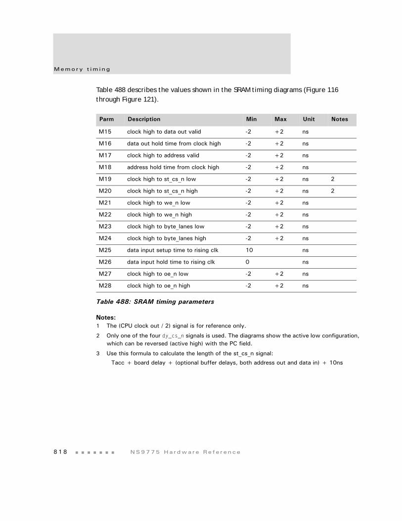
Memo ry t im i ng
8 1 8 NS9775 Ha r dwa r e Re f e r ence
Table 488 describes the values shown in the SRAM timing diagrams (Figure 116 through Figure 121).
Notes:1 The (CPU clock out / 2) signal is for reference only.
2 Only one of the four dy_cs_n signals is used. The diagrams show the active low configuration, which can be reversed (active high) with the PC field.
3 Use this formula to calculate the length of the st_cs_n signal:
Tacc + board delay + (optional buffer delays, both address out and data in) + 10ns
Parm Description Min Max Unit Notes
M15 clock high to data out valid -2 +2 ns
M16 data out hold time from clock high -2 +2 ns
M17 clock high to address valid -2 +2 ns
M18 address hold time from clock high -2 +2 ns
M19 clock high to st_cs_n low -2 +2 ns 2
M20 clock high to st_cs_n high -2 +2 ns 2
M21 clock high to we_n low -2 +2 ns
M22 clock high to we_n high -2 +2 ns
M23 clock high to byte_lanes low -2 +2 ns
M24 clock high to byte_lanes high -2 +2 ns
M25 data input setup time to rising clk 10 ns
M26 data input hold time to rising clk 0 ns
M27 clock high to oe_n low -2 +2 ns
M28 clock high to oe_n high -2 +2 ns
Table 488: SRAM timing parameters
www.d i g i . com 819
T im i ng
Static RAM read cycles with 0 wait states
Figure 116: Static RAM read cycles with 0 wait states timing
WTRD = 1
WOEN = 1
If the PB field is set to 1, all four byte_lane signals will go low for 32-bit, 16-bit, and 8-bit read cycles.
If the PB field is set to 0, the byte_lane signal will always be high.
M24M23
M28M27
M20M19
M18M17
M26M25
CPU clock / 2
data<31:0>
addr<27:0>
st_cs_n<3:0>
oe_n
byte_lane<3:0>
Memo ry t im i ng
8 2 0 NS9775 Ha r dwa r e Re f e r ence
Static RAM asynchronous page mode read, WTPG = 1
Figure 117: Static RAM asynchronous page mode read, WTPG = 1 timing
WTPG = 1
WTRD = 2
If the PB field is set to 1, all four byte_lane signals will go low for 32-bit, 16-bit, and 8-bit read cycles.
The asynchronous page mode will read 16 bytes in a page cycle. A 32-bit bus will do four 32-bit reads, as shown (3-2-2-2). A 16-bit bus will do eight 16-bit reads (3-2-2-2-3-2-2-2) per page cycle, and an 8-bit bus will do sixteen 8-bit reads (3-2-2-2-3-2-2-2-3-2-2-2-3-2-2-2) per page cycle. 3-2-2-2 is the example used here, but the WTRD and WTPG fields can set them differently.
Notes:1 The length of the first cycle in the page is determined by the WTRD field.
2 The length of the 2nd, 3rd, and 4th cycles is determined by the WTPG field.
3 This is the starting address. The least significant two bits will always be ‘00.’
4 The least significant two bits in the second cycle will always be ‘01.’
5 The least significant two bits in the third cycle will always be ‘10.’
6 The least significant two bits in the fourth cycle will always be ‘11.’
7 If the PB field is set to 0, the byte_lane signal will always be high during a read cycle.
Note-1 Note-2 Note-2 Note-2
M24M23
M28M27
M20M19
M18M18M17
M26M25
M26M25
Note-3 Note-4 Note-5 Note-6
Note-7
CPU clock / 2
data<31:0>
addr<27:0>
st_cs_n<3:0>
oe_n
byte_lane<3:0>
www.d i g i . com 821
T im i ng
Static RAM read cycle with configurable wait states
Figure 118: Static RAM read cycle with configurable wait states
WTRD = from 1 to 15
WOEN = from 0 to 15
If the PB field is set to 1, all four byte_lane signals will go low for 32-bit, 16-bit, and 8-bit read cycles.
If the PB field is set to 0, the byte_lane signal will always be high.
M24M23
M28M27
M20M19
M18M17
M26M25
Note-1
Note-1
Note-1
CPU clock / 2
data<31:0>
addr<27:0>
st_cs_n<3:0>
oe_n
byte_lane<3:0>
Memo ry t im i ng
8 2 2 NS9775 Ha r dwa r e Re f e r ence
Static RAM sequential write cycles
Figure 119: Static RAM sequential write cycles
WTWR = 0
WWEN = 0
During a 32-bit transfer, all four byte_lane signals will go low.
During a 16-bit transfer, two byte_lane signals will go low.
During an 8-bit transfer, only one byte_lane signal will go low.
Note:1 If the PB field is set to 0, the byte_lane signals will function as write enable signals and
the we_n signal will always be high.
M22M21
M24M23
M22M21
M20M19
M18M17
M16M15
Note1
CPU clock / 2
data<31:0>
addr<27:0>
st_cs_n<3:0>
we_n
byte_lane<3:0>
byte_lane[3:0] as WE*
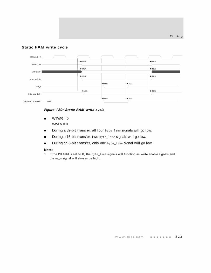
www.d i g i . com 823
T im i ng
Static RAM write cycle
Figure 120: Static RAM write cycle
WTWR = 0
WWEN = 0
During a 32-bit transfer, all four byte_lane signals will go low.
During a 16-bit transfer, two byte_lane signals will go low.
During an 8-bit transfer, only one byte_lane signal will go low.
Note:1 If the PB field is set to 0, the byte_lane signals will function as write enable signals and
the we_n signal will always be high.
M22M21
M24M23
M22M21
M20M19
M18M17
M16M15
Note-1
CPU clock / 2
data<31:0>
addr<27:0>
st_cs_n<3:0>
we_n
byte_lane<3:0>
byte_lane[3:0] as WE*
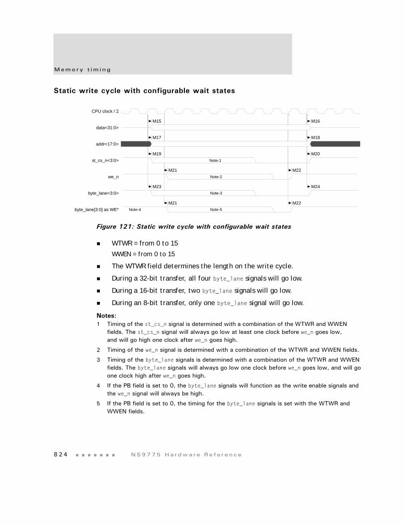
Memo ry t im i ng
8 2 4 NS9775 Ha r dwa r e Re f e r ence
Static write cycle with configurable wait states
Figure 121: Static write cycle with configurable wait states
WTWR = from 0 to 15
WWEN = from 0 to 15
The WTWR field determines the length on the write cycle.
During a 32-bit transfer, all four byte_lane signals will go low.
During a 16-bit transfer, two byte_lane signals will go low.
During an 8-bit transfer, only one byte_lane signal will go low.
Notes:1 Timing of the st_cs_n signal is determined with a combination of the WTWR and WWEN
fields. The st_cs_n signal will always go low at least one clock before we_n goes low, and will go high one clock after we_n goes high.
2 Timing of the we_n signal is determined with a combination of the WTWR and WWEN fields.
3 Timing of the byte_lane signals is determined with a combination of the WTWR and WWEN fields. The byte_lane signals will always go low one clock before we_n goes low, and will go one clock high after we_n goes high.
4 If the PB field is set to 0, the byte_lane signals will function as the write enable signals and the we_n signal will always be high.
5 If the PB field is set to 0, the timing for the byte_lane signals is set with the WTWR and WWEN fields.
M22M21
M24M23
M22M21
M20M19
M18M17
M16M15
Note-2
Note-3
Note-5Note-4
Note-1
CPU clock / 2
data<31:0>
addr<17:0>
st_cs_n<3:0>
we_n
byte_lane<3:0>
byte_lane[3:0] as WE*
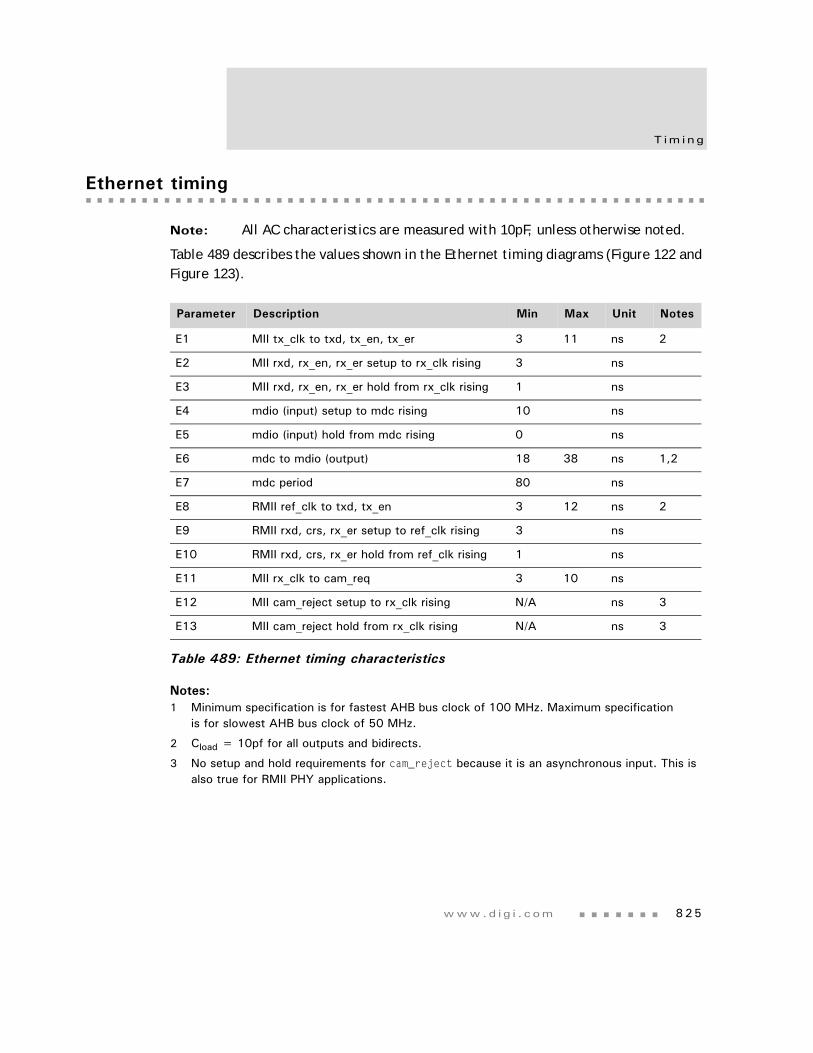
www.d i g i . com 825
T im i ng
Ethernet timing
Note: All AC characteristics are measured with 10pF, unless otherwise noted.
Table 489 describes the values shown in the Ethernet timing diagrams (Figure 122 and Figure 123).
Notes:1 Minimum specification is for fastest AHB bus clock of 100 MHz. Maximum specification
is for slowest AHB bus clock of 50 MHz.
2 Cload = 10pf for all outputs and bidirects.
3 No setup and hold requirements for cam_reject because it is an asynchronous input. This is also true for RMII PHY applications.
Parameter Description Min Max Unit Notes
E1 MII tx_clk to txd, tx_en, tx_er 3 11 ns 2
E2 MII rxd, rx_en, rx_er setup to rx_clk rising 3 ns
E3 MII rxd, rx_en, rx_er hold from rx_clk rising 1 ns
E4 mdio (input) setup to mdc rising 10 ns
E5 mdio (input) hold from mdc rising 0 ns
E6 mdc to mdio (output) 18 38 ns 1,2
E7 mdc period 80 ns
E8 RMII ref_clk to txd, tx_en 3 12 ns 2
E9 RMII rxd, crs, rx_er setup to ref_clk rising 3 ns
E10 RMII rxd, crs, rx_er hold from ref_clk rising 1 ns
E11 MII rx_clk to cam_req 3 10 ns
E12 MII cam_reject setup to rx_clk rising N/A ns 3
E13 MII cam_reject hold from rx_clk rising N/A ns 3
Table 489: Ethernet timing characteristics
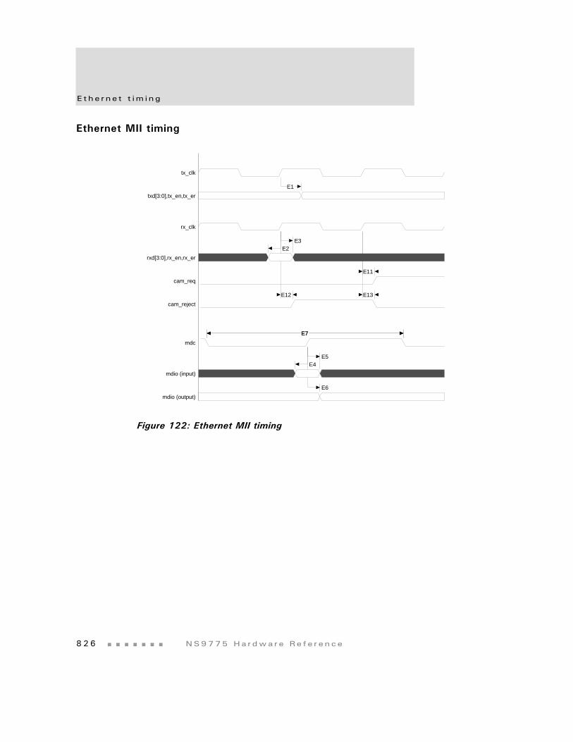
E t he r n e t t im i ng
8 2 6 NS9775 Ha r dwa r e Re f e r ence
Ethernet MII timing
Figure 122: Ethernet MII timing
E6
E5E4
E3E2
E1
E7E7
E13E12
E11
tx_clk
txd[3:0],tx_en,tx_er
rx_clk
rxd[3:0],rx_en,rx_er
cam_req
cam_reject
mdc
mdio (input)
mdio (output)
www.d i g i . com 827
T im i ng
Ethernet RMII timing
Figure 123: Ethernet RMII timing
E6
E5E4
E10E9
E8
E7E7
ref_clk
txd[1:0],tx_en
rxd[1:0],crs,rx_er
mdc
mdio (input)
mdio (output)
PC I t im i ng
8 2 8 NS9775 Ha r dwa r e Re f e r ence
PCI timing
Note: All AC characteristics are measured with 10pF, unless otherwise noted.
Table 490 and Table 491 describe the values shown in the PCI timing diagrams (Figure 124 through Figure 130).
Notes:1 Parameters same for bussed and point-to-point signals.
2 CLOAD = 10pf on all outputs
3 pci_clk_out high and low times specified as 50% of the clock period +/-1 ns.
Parameter Description Min Max Units Notes
P1 pci_clk_in to signal valid delay 2 9 ns 1,2
P2 Input setup to pci_clk_in 5 ns 1
P3 Input hold from pci_clk_in 0 ns
P4 pci_clk_in to signal active 2 ns 2
P5 pci_clk_in to signal float 28 ns 2
P6 pci_clk_out high time 50%-1 50%+1 ns 3
P7 pci_clk_out low time 50%-1 50%+1 ns 3
P8 pci_clk_in cycle time 30 ns
P9 pci_clk_in high time 11 ns
P10 pci_clk_in low time 11 ns
Table 490: PCI timing characteristics
www.d i g i . com 829
T im i ng
Notes:1 Minimum times are specified with 0pf and maximum times are specified with 30pf.
2 pci_clk_out high and low times specified as 50% of the clock period +/-1 ns.
Parameter Description Min Max Units Notes
P1 pci_clk_in to signal valid delay 2 10 ns 1
P2 Input setup to pci_clk_in 5 ns 1
P3 Input hold from pci_clk_in 0 ns
P4 pci_clk_in to signal active 2 ns 1
P5 pci_clk_in to signal float 28 ns 1
P6 pci_clk_out high time 50%-1 50%+1 ns 2
P7 pci_clk_out low time 50%-1 50%+1 ns 2
P8 pci_clk_in cycle time 30 ns
P9 pci_clk_in high time 11 ns
P10 pci_clk_in low time 11 ns
Table 491: CardBus timing characteristics
PC I t im i ng
8 3 0 NS9775 Ha r dwa r e Re f e r ence
Internal PCI arbiter timing
Figure 124: Internal PCI arbiter timing
PCI burst write from NS9775 timing
Figure 125: PCI burst write from NS9775 timing
Note: The functional timing for trdy_n and devsel_n shows the fastest possible response from the target.
data0 addr
P1
P2
P3
Master 1 CycleMaster 1 CycleMaster 2 CycleMaster 2 CycleMaster 1 CycleMaster 1 Cycle
Switch MasterSwitch Master
addr data1 data2 data0 addr data0
pci_clk_in
frame_n
irdy_n
ad[31:0]
pci_arb_req_1_n
pci_arb_req_2_n
pci_arb_gnt_1_n
pci_arb_gnt_2_n
P3P2
P3P2
P1
P1
P5P1P4
P1
byte enablescmd
addr data0 data1 data2 data3 data4 data5 data6 data7
pci_clk_in
frame_n
ad[31:0]
cbe_n[3:0]
irdy_n
trdy_n
devsel_n
www.d i g i . com 831
T im i ng
PCI burst read from NS9775 timing
Figure 126: PCI burst read from NS9775 timing
Note: The functional timing for trdy_n, devsel_n, and the read data on ad[31:0] shows the fastest possible response from the target.
PCI burst write to NS9775 timing
Figure 127: PCI burst write to NS9775 timing
P3P2
P3P2
P1
P1
P3P2P5P1P4
P1
byte enablescmd
addr data0 data1 data2 data3 data4 data5 data6 data7
pci_clk_in
frame_n
ad[31:0]
cbe_n[3:0]
irdy_n
trdy_n
devsel_n
3x pci_clk_inP1
P1
P3P2
P3P2
P3P2
P3P2
byte enablescmd
addr data0 data1 data2 data3 data4 data5 data6 data7
pci_clk_in
frame_n
ad[31:0]
cbe_n[3:0]
irdy_n
trdy_n
devsel_n
PC I t im i ng
8 3 2 NS9775 Ha r dwa r e Re f e r ence
PCI burst read to NS9775 timing
Figure 128: PCI burst read to NS9775 timing
Note: The functional timing for valid read data on ad[31:0] is just an example. The actual response time will depend on when the PCI bridge gets access to the AHB bus internal to NS9775.
PCI clock timing
Figure 129: pci_clock_out timing
Figure 130: pci_clk_in timing
3x pci_clk_inP1
P1
P3P2
P3P2
P5P1P4P2
P3P2
byte enablescmd
addr data0 data1 data2 data3 data4 data5 data6 data7
N t
pci_clk_in
frame_n
ad[31:0]
cbe_n[3:0]
irdy_n
trdy_n
devsel_n
P7P7P6P6pci_clk_out
P10P8
P10P9P9P8
pci_clk_in
www.d i g i . com 833
T im i ng
I2C timing
Note: All AC characteristics are measured with 10pF, unless otherwise noted.
Table 492 describes the values shown in the I2C timing diagram (Figure 131).
Figure 131: I2C timing
Standard mode Fast mode
Parm Description Min Max Min Max Unit
C1 iic_sda to iic_scl START hold time 4.0 0.6 μs
C2 iic_scl low period 4.7 1.3 μs
C3 iic_scl high period 4.7 1.3 μs
C4 iic_scl to iic_sda DATA hold time 0 0 μs
C5 iic_sda to iic_scl DATA setup time 250 100 ns
C6 iic_scl to iic_sda START setup time 4.7 0.6 μs
C7 iic_scl to iic_sda STOP setup time 4.0 0.6 μs
Table 492: I2C timing parameters
C4 C6 C7
C1 C2C5
C3
iic_sda
iic_scl
LCD t im i ng
8 3 4 NS9775 Ha r dwa r e Re f e r ence
LCD timing
Note: All AC characteristics are measured with 10pF, unless otherwise noted.
Table 493 describes the values shown in the LCD timing diagrams (Figure 132 through Figure 138).
Parm Description Register Value Units
L1 Horizontal front porch blanking
LCDTiming0 HFP+1 CLCP periods
L2 Horizontal sync width LCDTiming0 HSW+1 CLCP periods
L3 Horizontal period N/A L1+L2+L15+L4 CLCP periods
L4 Horizontal backporch LCDTiming0 HBP+1 CLCP periods
L5 TFT active line LCDTiming0 16*(PPL+1)(see note 3)
CLCP periods
L6 LCD panel clock frequency LCDTiming1 For BCD=0:CLCDCLK/(PCD+2)For BCD=1:CLCDCLK (see note 1)
MHz
L7 TFT vertical sync width LCDTiming1 VSW+1 H lines
L8 TFT vertical lines/frame N/A L7+L9+L10+L11 H lines
L9 TFT vertical back porch LCDTiming1 VBP H lines
L10 TFT vertical front porch LCDTiming1 VFP H lines
L11 Active lines/frame LCDTiming1 LPP+1 H lines
L12 STN HSYNC inactive to VSYNC active
LCDTiming0 HBP+1 CLCP periods
L13 STN vertical sync width N/A 1 H lines
L14 STN vertical lines/frame N/A L11+L16 H lines
L15 STN active line LCDTiming2 CPL+1 (see note 4) CLCP periods
L16 STN vertical blanking LCDTiming1 VSW+VFP+VBP+1 H lines
L17 STN CLCP inactive to HSYNC active
LCDTiming0 HFP+1.5 CLCP periods
Table 493: LCD timing parameters
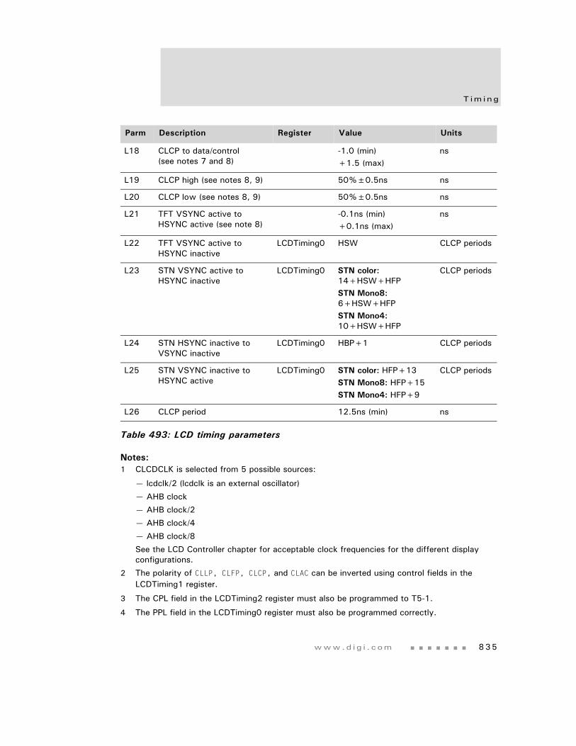
www.d i g i . com 835
T im i ng
Notes:1 CLCDCLK is selected from 5 possible sources:
— lcdclk/2 (lcdclk is an external oscillator)
— AHB clock
— AHB clock/2
— AHB clock/4
— AHB clock/8
See the LCD Controller chapter for acceptable clock frequencies for the different display configurations.
2 The polarity of CLLP, CLFP, CLCP, and CLAC can be inverted using control fields in the LCDTiming1 register.
3 The CPL field in the LCDTiming2 register must also be programmed to T5-1.
4 The PPL field in the LCDTiming0 register must also be programmed correctly.
L18 CLCP to data/control(see notes 7 and 8)
-1.0 (min)+1.5 (max)
ns
L19 CLCP high (see notes 8, 9) 50%±0.5ns ns
L20 CLCP low (see notes 8, 9) 50%±0.5ns ns
L21 TFT VSYNC active to HSYNC active (see note 8)
-0.1ns (min)+0.1ns (max)
ns
L22 TFT VSYNC active to HSYNC inactive
LCDTiming0 HSW CLCP periods
L23 STN VSYNC active to HSYNC inactive
LCDTiming0 STN color: 14+HSW+HFPSTN Mono8: 6+HSW+HFPSTN Mono4: 10+HSW+HFP
CLCP periods
L24 STN HSYNC inactive to VSYNC inactive
LCDTiming0 HBP+1 CLCP periods
L25 STN VSYNC inactive to HSYNC active
LCDTiming0 STN color: HFP+13STN Mono8: HFP+15STN Mono4: HFP+9
CLCP periods
L26 CLCP period 12.5ns (min) ns
Parm Description Register Value Units
Table 493: LCD timing parameters
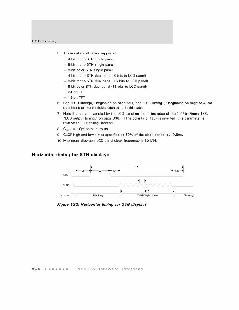
LCD t im i ng
8 3 6 NS9775 Ha r dwa r e Re f e r ence
5 These data widths are supported:
— 4-bit mono STN single panel
— 8-bit mono STN single panel
— 8-bit color STN single panel
— 4-bit mono STN dual panel (8 bits to LCD panel)
— 8-bit mono STN dual panel (16 bits to LCD panel)
— 8-bit color STN dual panel (16 bits to LCD panel)
— 24-bit TFT
— 18-bit TFT
6 See "LCDTiming0," beginning on page 591, and "LCDTiming1," beginning on page 594, for definitions of the bit fields referred to in this table.
7 Note that data is sampled by the LCD panel on the falling edge of the CLCP in Figure 138, "LCD output timing," on page 838). If the polarity of CLCP is inverted, this parameter is relative to CLCP falling, instead.
8 Cload = 10pf on all outputs.
9 CLCP high and low times specified as 50% of the clock period +/- 0.5ns.
10 Maximum allowable LCD panel clock frequency is 80 MHz.
Horizontal timing for STN displays
Figure 132: Horizontal timing for STN displays
L15L15
L6L6
L17L3
L4L2L1L3
L2
Valid Display DataBlanking Blanking
CLLP
CLCP
CLD[7:0]
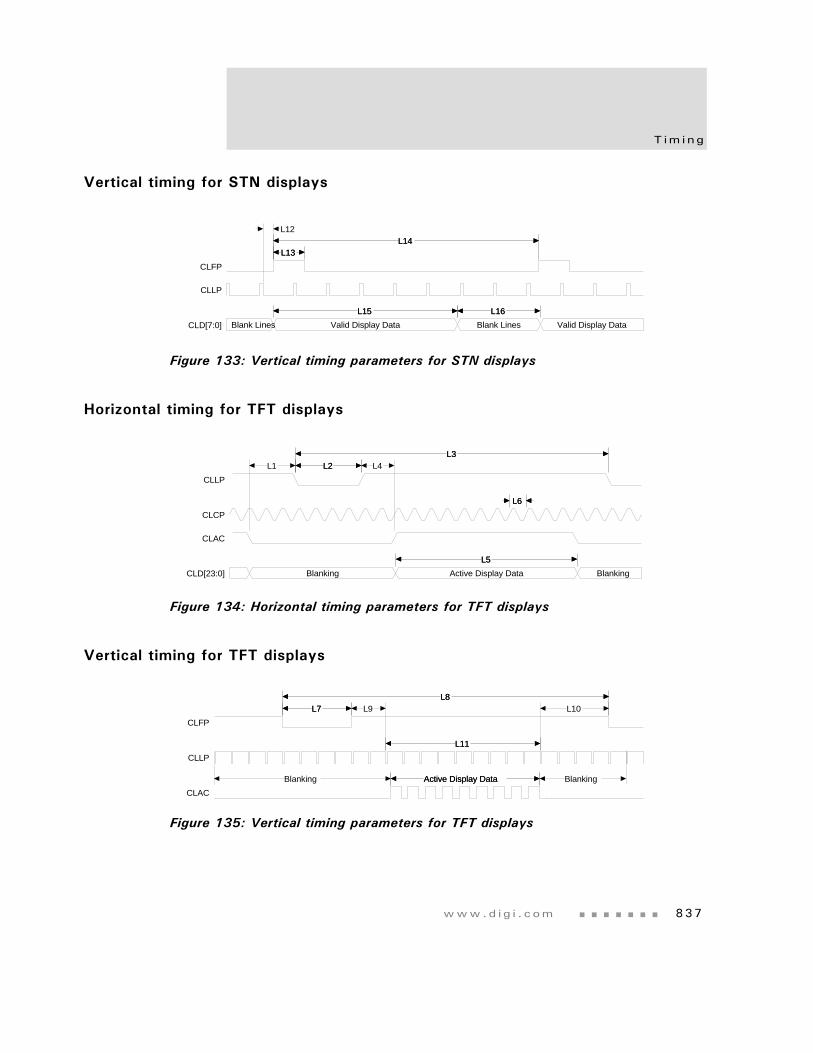
www.d i g i . com 837
T im i ng
Vertical timing for STN displays
Figure 133: Vertical timing parameters for STN displays
Horizontal timing for TFT displays
Figure 134: Horizontal timing parameters for TFT displays
Vertical timing for TFT displays
Figure 135: Vertical timing parameters for TFT displays
L16L16L15L15
L14L13
L12L14
L13
Valid Display Data Valid Display DataBlank LinesBlank Lines
CLFP
CLLP
CLD[7:0]
L5L5
L6L6
L3L4L2
L3L1 L2
Active Display DataBlanking Blanking
CLLP
CLCP
CLAC
CLD[23:0]
Active Display Data BlankingActive Display DataBlanking
L11L11
L10L8
L9L7L8
L7CLFP
CLLP
CLAC
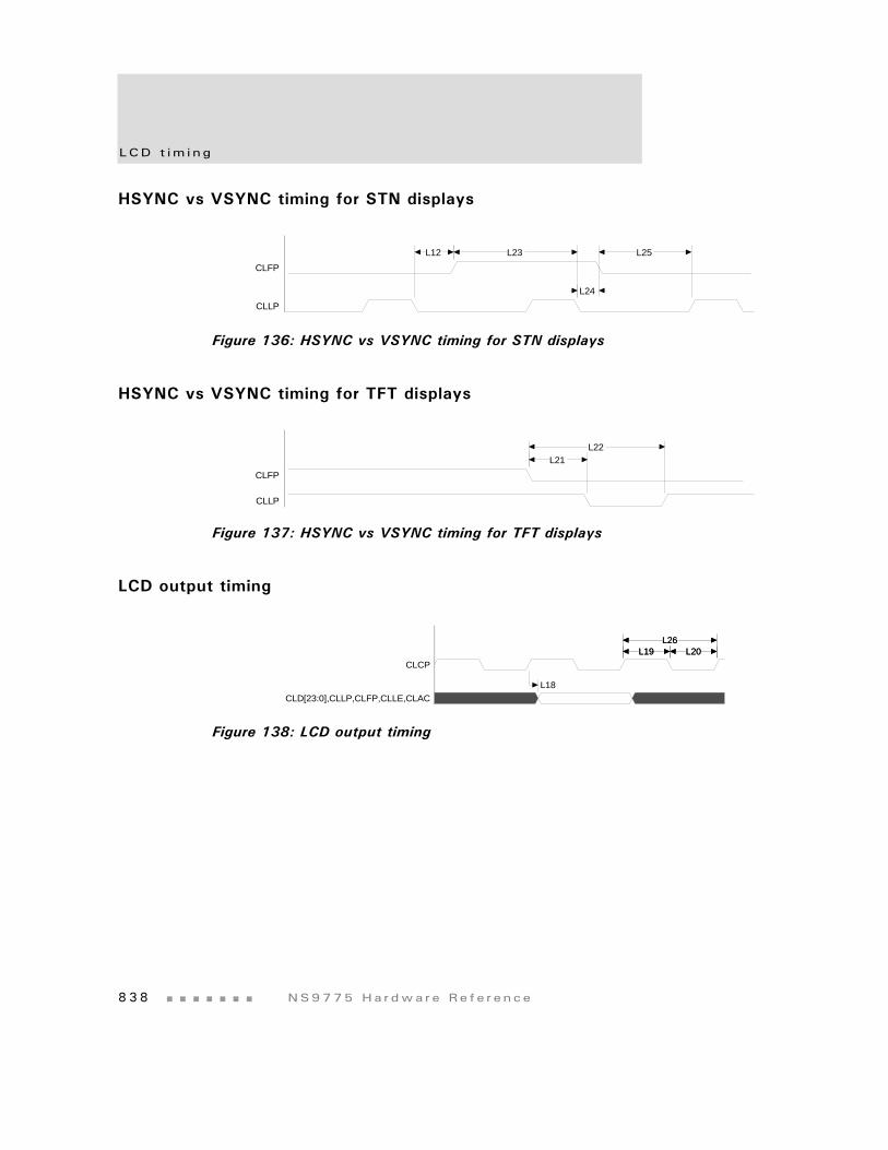
LCD t im i ng
8 3 8 NS9775 Ha r dwa r e Re f e r ence
HSYNC vs VSYNC timing for STN displays
Figure 136: HSYNC vs VSYNC timing for STN displays
HSYNC vs VSYNC timing for TFT displays
Figure 137: HSYNC vs VSYNC timing for TFT displays
LCD output timing
Figure 138: LCD output timing
L24
L25L23L12CLFP
CLLP
L22L21
CLFP
CLLP
L18
L26L20L20L19
L26L19
CLCP
CLD[23:0],CLLP,CLFP,CLLE,CLAC
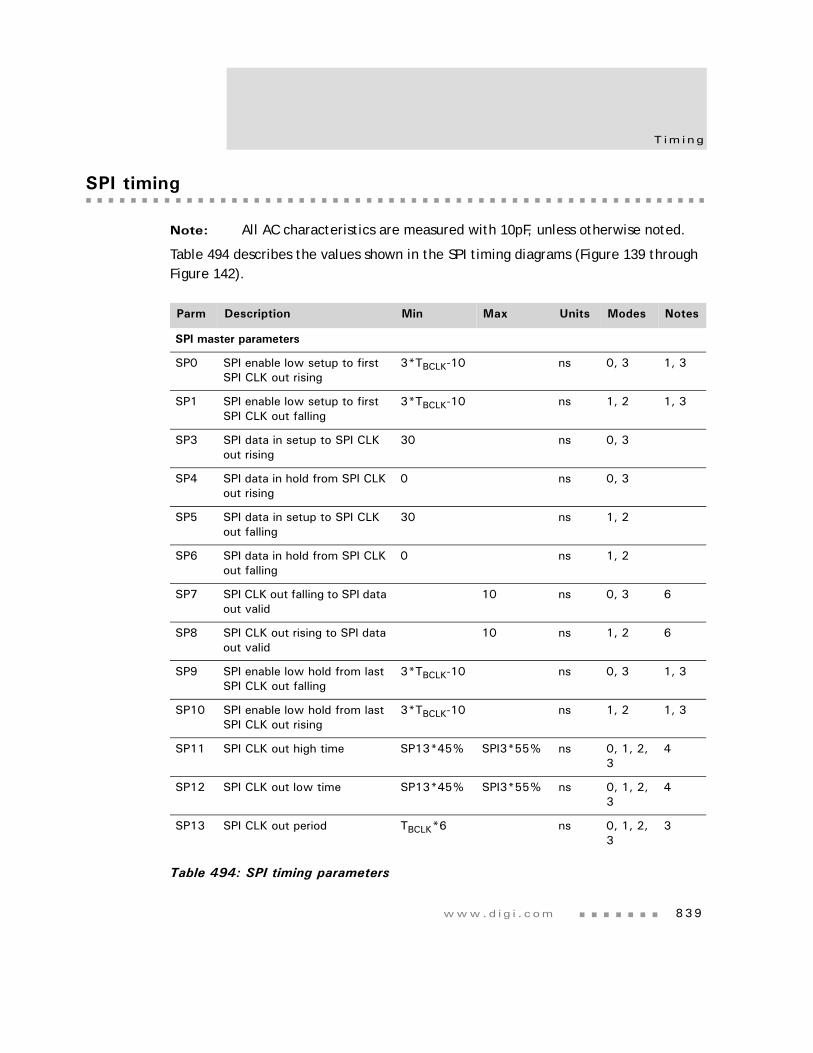
www.d i g i . com 839
T im i ng
SPI timing
Note: All AC characteristics are measured with 10pF, unless otherwise noted.
Table 494 describes the values shown in the SPI timing diagrams (Figure 139 through Figure 142).
Parm Description Min Max Units Modes Notes
SPI master parameters
SP0 SPI enable low setup to first SPI CLK out rising
3*TBCLK-10 ns 0, 3 1, 3
SP1 SPI enable low setup to first SPI CLK out falling
3*TBCLK-10 ns 1, 2 1, 3
SP3 SPI data in setup to SPI CLK out rising
30 ns 0, 3
SP4 SPI data in hold from SPI CLK out rising
0 ns 0, 3
SP5 SPI data in setup to SPI CLK out falling
30 ns 1, 2
SP6 SPI data in hold from SPI CLK out falling
0 ns 1, 2
SP7 SPI CLK out falling to SPI data out valid
10 ns 0, 3 6
SP8 SPI CLK out rising to SPI data out valid
10 ns 1, 2 6
SP9 SPI enable low hold from last SPI CLK out falling
3*TBCLK-10 ns 0, 3 1, 3
SP10 SPI enable low hold from last SPI CLK out rising
3*TBCLK-10 ns 1, 2 1, 3
SP11 SPI CLK out high time SP13*45% SPI3*55% ns 0, 1, 2, 3
4
SP12 SPI CLK out low time SP13*45% SPI3*55% ns 0, 1, 2, 3
4
SP13 SPI CLK out period TBCLK*6 ns 0, 1, 2, 3
3
Table 494: SPI timing parameters
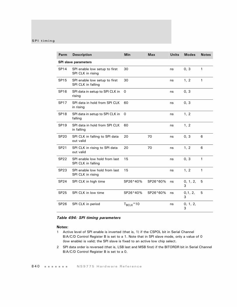
SP I t im i ng
8 4 0 NS9775 Ha r dwa r e Re f e r ence
Notes:1 Active level of SPI enable is inverted (that is, 1) if the CSPOL bit in Serial Channel
B/A/C/D Control Register B is set to a 1. Note that in SPI slave mode, only a value of 0 (low enable) is valid; the SPI slave is fixed to an active low chip select.
2 SPI data order is reversed (that is, LSB last and MSB first) if the BITORDR bit in Serial Channel B/A/C/D Control Register B is set to a 0.
SPI slave parameters
SP14 SPI enable low setup to first SPI CLK in rising
30 ns 0, 3 1
SP15 SPI enable low setup to first SPI CLK in falling
30 ns 1, 2 1
SP16 SPI data in setup to SPI CLK in rising
0 ns 0, 3
SP17 SPI data in hold from SPI CLK in rising
60 ns 0, 3
SP18 SPI data in setup to SPI CLK in falling
0 ns 1, 2
SP19 SPI data in hold from SPI CLK in falling
60 ns 1, 2
SP20 SPI CLK in falling to SPI data out valid
20 70 ns 0, 3 6
SP21 SPI CLK in rising to SPI data out valid
20 70 ns 1, 2 6
SP22 SPI enable low hold from last SPI CLK in falling
15 ns 0, 3 1
SP23 SPI enable low hold from last SPI CLK in rising
15 ns 1, 2 1
SP24 SPI CLK in high time SP26*40% SP26*60% ns 0, 1, 2, 3
5
SP25 SPI CLK in low time SP26*40% SP26*60% ns 0,1, 2, 3
5
SP26 SPI CLK in period TBCLK*10 ns 0, 1, 2, 3
Parm Description Min Max Units Modes Notes
Table 494: SPI timing parameters
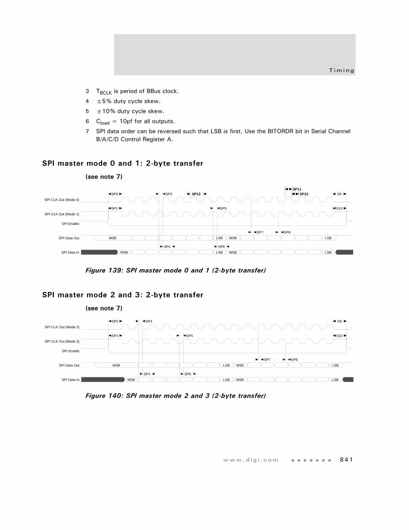
www.d i g i . com 841
T im i ng
3 TBCLK is period of BBus clock.
4 ±5% duty cycle skew.
5 ±10% duty cycle skew.
6 Cload = 10pf for all outputs.
7 SPI data order can be reversed such that LSB is first. Use the BITORDR bit in Serial ChannelB/A/C/D Control Register A.
SPI master mode 0 and 1: 2-byte transfer
(see note 7)
Figure 139: SPI master mode 0 and 1 (2-byte transfer)
SPI master mode 2 and 3: 2-byte transfer
(see note 7)
Figure 140: SPI master mode 2 and 3 (2-byte transfer)
MSB LSB MSB LSB
MSB LSB MSB LSBSP6SP4
SP8SP7
S10SP5SP1
S9SP12SP12SP11SP11
SP13SP13SP3SP0SPI CLK Out (Mode 0)
SPI CLK Out (Mode 1)
SPI Enable
SPI Data Out
SPI Data In
MSB LSB MSB LSB
MSB LSB MSB LSBSP6SP4
SP8SP7
S10SP5SP1
S9SP3SP0SPI CLK Out (Mode 2)
SPI CLK Out (Mode 3)
SPI Enable
SPI Data Out
SPI Data In
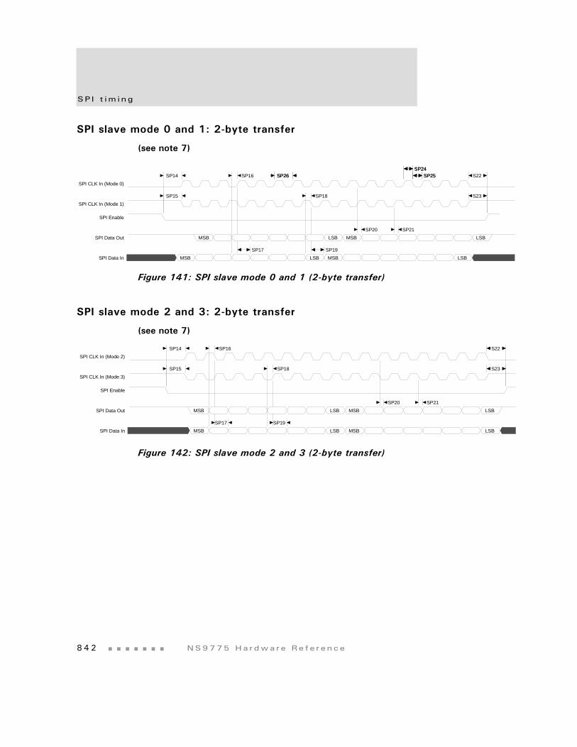
SP I t im i ng
8 4 2 NS9775 Ha r dwa r e Re f e r ence
SPI slave mode 0 and 1: 2-byte transfer
(see note 7)
Figure 141: SPI slave mode 0 and 1 (2-byte transfer)
SPI slave mode 2 and 3: 2-byte transfer
(see note 7)
Figure 142: SPI slave mode 2 and 3 (2-byte transfer)
MSB LSB MSB LSB
MSB LSB MSB LSBSP19SP17
SP21SP20
S23SP18SP15
S22SP25SP25SP24SP24
SP26SP26SP16SP14SPI CLK In (Mode 0)
SPI CLK In (Mode 1)
SPI Enable
SPI Data Out
SPI Data In
MSB LSB MSB LSB
MSB LSB MSB LSBSP19SP17
SP21SP20
S23SP18SP15
S22SP16SP14SPI CLK In (Mode 2)
SPI CLK In (Mode 3)
SPI Enable
SPI Data Out
SPI Data In
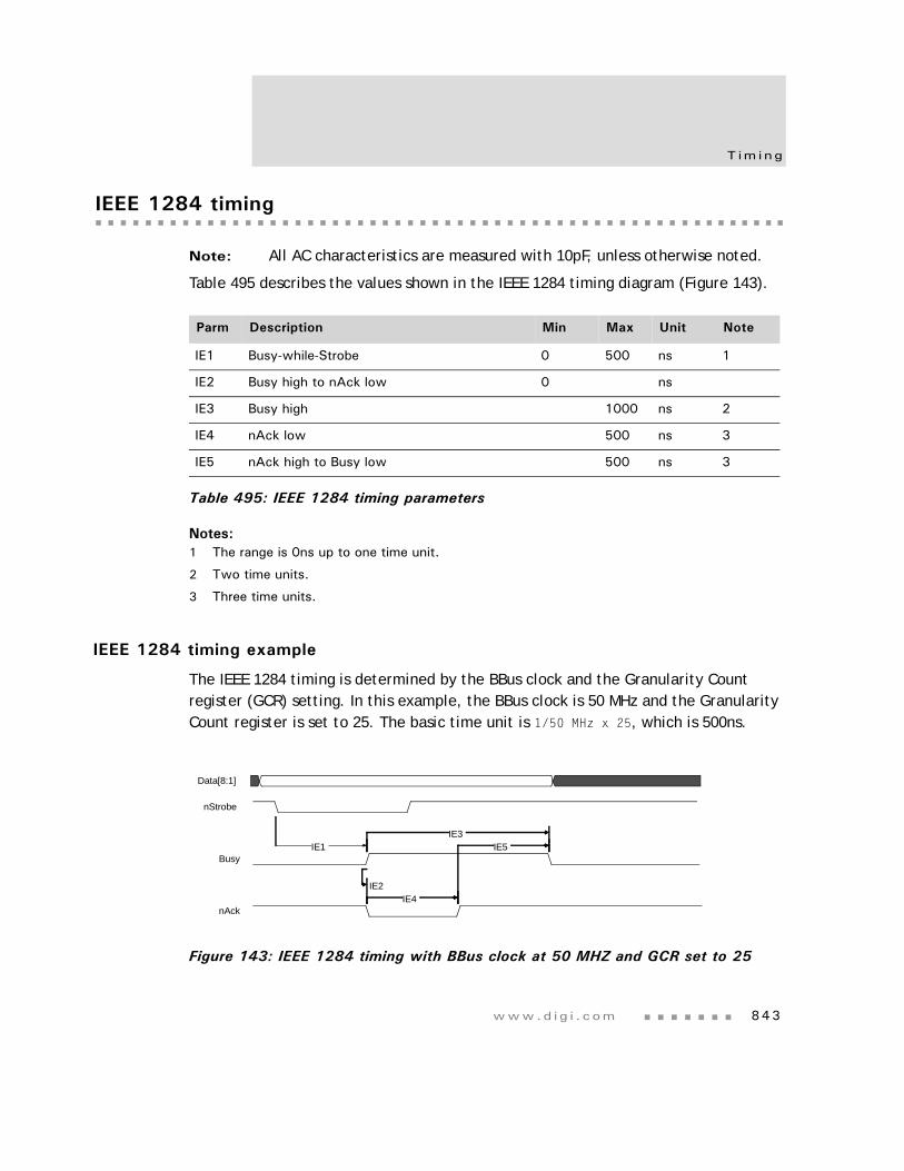
www.d i g i . com 843
T im i ng
IEEE 1284 timing
Note: All AC characteristics are measured with 10pF, unless otherwise noted.
Table 495 describes the values shown in the IEEE 1284 timing diagram (Figure 143).
Notes:1 The range is 0ns up to one time unit.
2 Two time units.
3 Three time units.
IEEE 1284 timing example
The IEEE 1284 timing is determined by the BBus clock and the Granularity Count register (GCR) setting. In this example, the BBus clock is 50 MHz and the Granularity Count register is set to 25. The basic time unit is 1/50 MHz x 25, which is 500ns.
Figure 143: IEEE 1284 timing with BBus clock at 50 MHZ and GCR set to 25
Parm Description Min Max Unit Note
IE1 Busy-while-Strobe 0 500 ns 1
IE2 Busy high to nAck low 0 ns
IE3 Busy high 1000 ns 2
IE4 nAck low 500 ns 3
IE5 nAck high to Busy low 500 ns 3
Table 495: IEEE 1284 timing parameters
IE1IE3
IE5
IE2IE4
Data[8:1]
nStrobe
Busy
nAck
USB t im i ng
8 4 4 NS9775 Ha r dwa r e Re f e r ence
USB timing
Table 496 and Table 497 describe the values shown in the USB timing diagrams(Figure 144 through Figure 146).
Notes:1 Load shown in Figure 145, "USB full speed load," on page 845.
2 U1/U2.
3 Includes resistance of 27 ohm ±2 ohm external series resistor.
4 Load shown in Figure 146, "USB low speed load," on page 846.
5 Excluding the first transition from the idle state.
Parm Description Min Max Unit Notes
U1 Rise time (10% – 90%) 4 20 ns 1
U2 Fall time (10% – 90%) 4 20 ns 1
U3 Differential rise and fall time matching 90 111.11 % 2, 5
U4 Driver output resistance 28 44 ohms 3
Table 496: USB full speed timing parameters
Parm Description Min Max Unit Notes
U1 Rise time (10% – 90%) 75 300 ns 4
U2 Fall time (10% – 90%) 75 300 ns 4
U3 Differential rise and fall time matching 80 125 % 2, 5
Table 497: USB low speed timing parameters
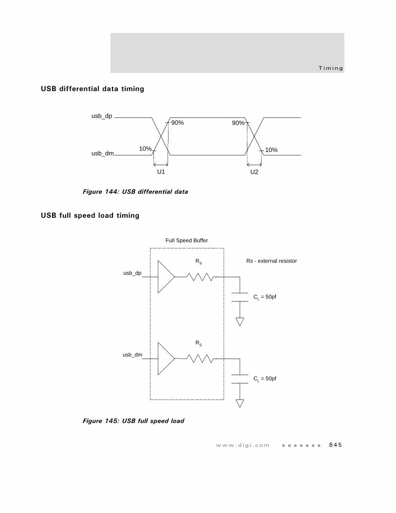
www.d i g i . com 845
T im i ng
USB differential data timing
Figure 144: USB differential data
USB full speed load timing
Figure 145: USB full speed load
U1
10%
90% 90%
10%
U2
usb_dp
usb_dm
CL = 50pf
RS
usb_dp
CL = 50pf
RS
usb_dm
Full Speed Buffer
Rs - external resistor
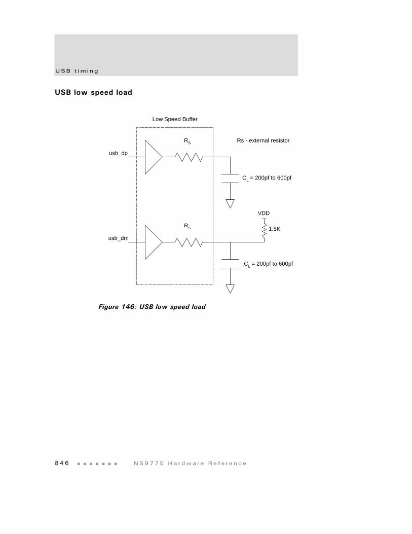
USB t im i ng
8 4 6 NS9775 Ha r dwa r e Re f e r ence
USB low speed load
Figure 146: USB low speed load
CL = 200pf to 600pf
RS
usb_dp
RS
usb_dm
Low Speed Buffer
Rs - external resistor
CL = 200pf to 600pf
VDD
1.5K
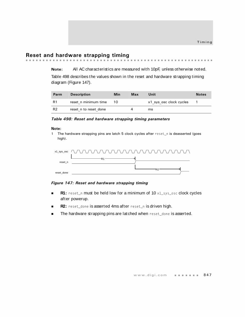
www.d i g i . com 847
T im i ng
Reset and hardware strapping timing
Note: All AC characteristics are measured with 10pF, unless otherwise noted.
Table 498 describes the values shown in the reset and hardware strapping timing diagram (Figure 147).
Note:1 The hardware strapping pins are latch 5 clock cycles after reset_n is deasserted (goes
high).
Figure 147: Reset and hardware strapping timing
R1: reset_n must be held low for a minimum of 10 x1_sys_osc clock cycles after powerup.
R2: reset_done is asserted 4ms after reset_n is driven high.
The hardware strapping pins are latched when reset_done is asserted.
Parm Description Min Max Unit Notes
R1 reset_n minimum time 10 x1_sys_osc clock cycles 1
R2 reset_n to reset_done 4 ms
Table 498: Reset and hardware strapping timing parameters
R1
R2
x1_sys_osc
reset_n
reset_done
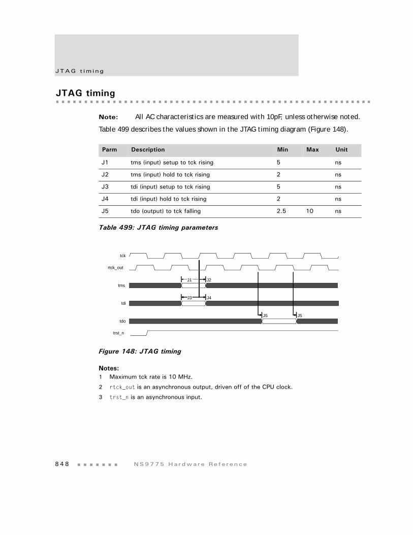
JTAG t im i ng
8 4 8 NS9775 Ha r dwa r e Re f e r ence
JTAG timing
Note: All AC characteristics are measured with 10pF, unless otherwise noted.
Table 499 describes the values shown in the JTAG timing diagram (Figure 148).
Figure 148: JTAG timing
Notes:1 Maximum tck rate is 10 MHz.
2 rtck_out is an asynchronous output, driven off of the CPU clock.
3 trst_n is an asynchronous input.
Parm Description Min Max Unit
J1 tms (input) setup to tck rising 5 ns
J2 tms (input) hold to tck rising 2 ns
J3 tdi (input) setup to tck rising 5 ns
J4 tdi (input) hold to tck rising 2 ns
J5 tdo (output) to tck falling 2.5 10 ns
Table 499: JTAG timing parameters
J1 J2
J3 J4
J5 J5
tck
rtck_out
tms
tdi
tdo
trst_n
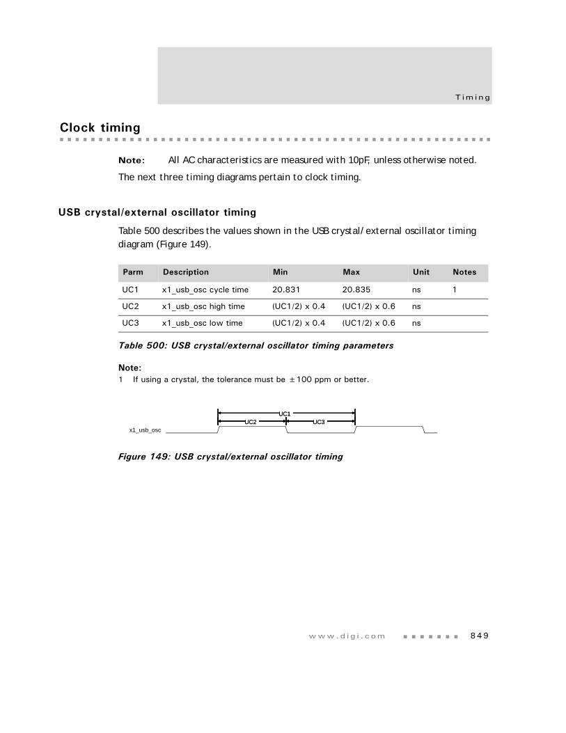
www.d i g i . com 849
T im i ng
Clock timing
Note: All AC characteristics are measured with 10pF, unless otherwise noted.
The next three timing diagrams pertain to clock timing.
USB crystal/external oscillator timing
Table 500 describes the values shown in the USB crystal/external oscillator timing diagram (Figure 149).
Note:1 If using a crystal, the tolerance must be ±100 ppm or better.
Figure 149: USB crystal/external oscillator timing
Parm Description Min Max Unit Notes
UC1 x1_usb_osc cycle time 20.831 20.835 ns 1
UC2 x1_usb_osc high time (UC1/2) x 0.4 (UC1/2) x 0.6 ns
UC3 x1_usb_osc low time (UC1/2) x 0.4 (UC1/2) x 0.6 ns
Table 500: USB crystal/external oscillator timing parameters
UC1UC2UC2 UC3
UC1UC3
x1_usb_osc
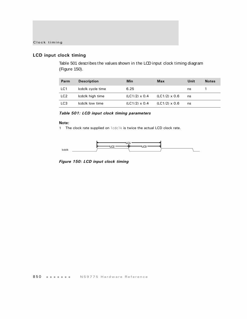
C l ock t im i ng
8 5 0 NS9775 Ha r dwa r e Re f e r ence
LCD input clock timing
Table 501 describes the values shown in the LCD input clock timing diagram(Figure 150).
Note:1 The clock rate supplied on lcdclk is twice the actual LCD clock rate.
Figure 150: LCD input clock timing
Parm Description Min Max Unit Notes
LC1 lcdclk cycle time 6.25 ns 1
LC2 lcdclk high time (LC1/2) x 0.4 (LC1/2) x 0.6 ns
LC3 lcdclk low time (LC1/2) x 0.4 (LC1/2) x 0.6 ns
Table 501: LCD input clock timing parameters
LC2LC1
LC2 LC3LC1
LC3lcdclk
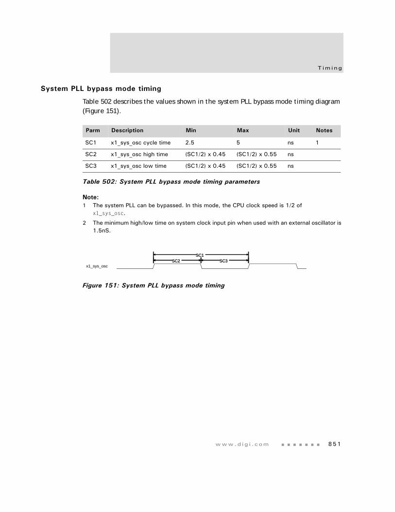
www.d i g i . com 851
T im i ng
System PLL bypass mode timing
Table 502 describes the values shown in the system PLL bypass mode timing diagram (Figure 151).
Note:1 The system PLL can be bypassed. In this mode, the CPU clock speed is 1/2 of
x1_sys_osc.
2 The minimum high/low time on system clock input pin when used with an external oscillator is 1.5nS.
Figure 151: System PLL bypass mode timing
Parm Description Min Max Unit Notes
SC1 x1_sys_osc cycle time 2.5 5 ns 1
SC2 x1_sys_osc high time (SC1/2) x 0.45 (SC1/2) x 0.55 ns
SC3 x1_sys_osc low time (SC1/2) x 0.45 (SC1/2) x 0.55 ns
Table 502: System PLL bypass mode timing parameters
SC1SC2SC2 SC3
SC1SC3
x1_sys_osc

853
PackagingC H A P T E R 1 8
The NS9775 is a complete system-on-chip processor, and includes Ethernet, display support, and a robust peripheral set.
NS9775 dimensions and pinout are shown on the following pages.
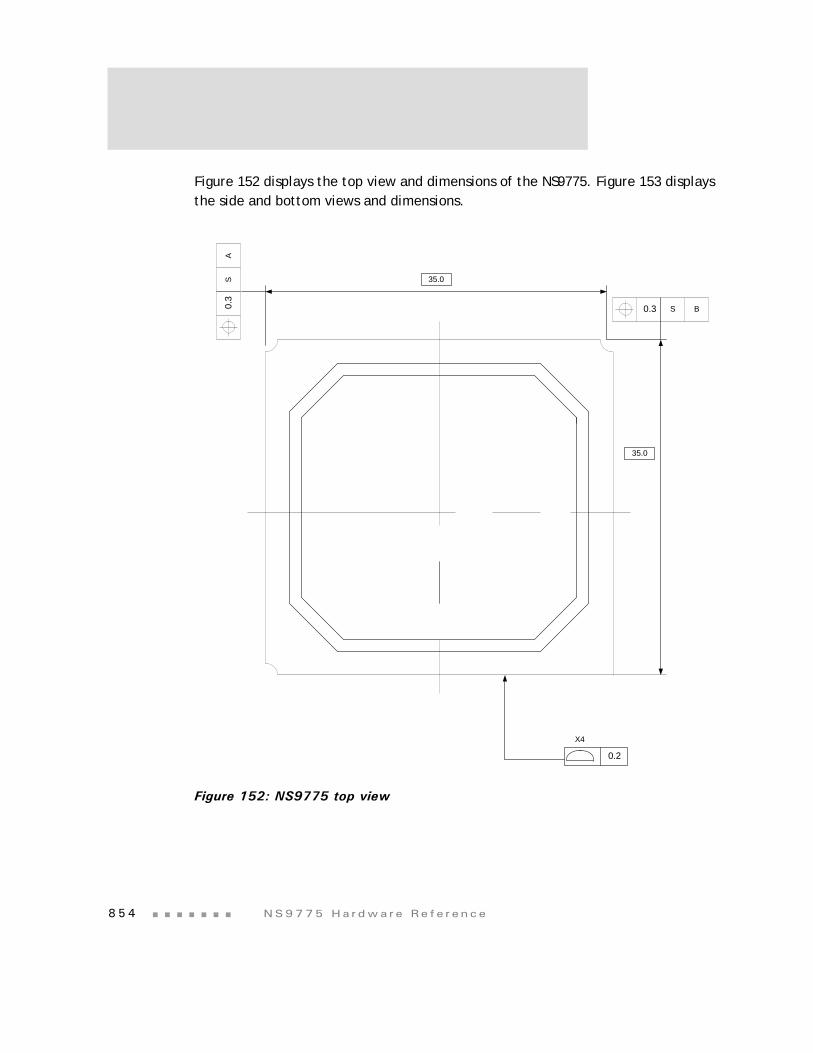
8 5 4 NS9775 Ha r dwa r e Re f e r ence
Figure 152 displays the top view and dimensions of the NS9775. Figure 153 displays the side and bottom views and dimensions.
Figure 152: NS9775 top view
35.0
35.0
0.3
AS
0.3 BS
0.2
X4
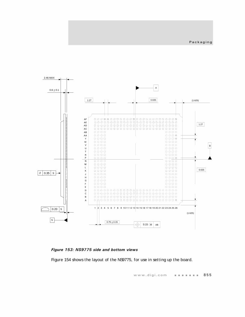
www.d i g i . com 855
Packag i ng
Figure 153: NS9775 side and bottom views
Figure 154 shows the layout of the NS9775, for use in setting up the board.
0.20 S
// 0.35 S
0.6 + 0.1
2.46 MAX
S
A
B
CD
EF
GHJ
KLMNPR
TUVWY
AAAB
AC
ADAEAF
2 3 4 5 61 7 8 9 10 11 12 13 14 15 16 17 18 19 20 21 22 23 24 25 26
0.635 (1.625)
1.27
0.635
A
B
(1.625)
0.75 + 0.150.15 M AB
1.27
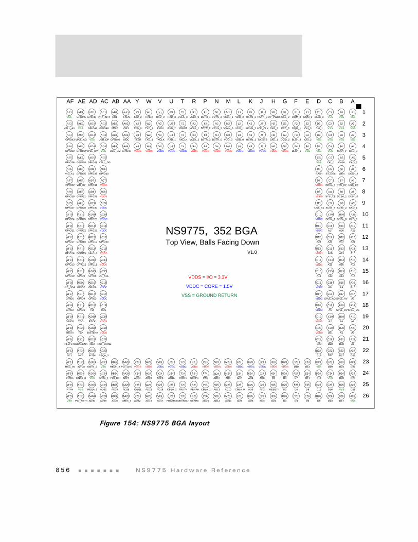
8 5 6 NS9775 Ha r dwa r e Re f e r ence
Figure 154: NS9775 BGA layout
W4
AD21
GPIO40
W
D4 A4
D26
D6
C17
TCK
K26
VDDS
AC21
CKE_0
J3
A11
K24
VDDS
AB23
TXD_0
B25
SYS_X2
L3
AF17
GPIO27
AC26
AE24
D7
P
GPIO23 VDDC
W23
GNTn_1
AC1
C22
C23
B18
N26
IDSEL
DQM_0
C5
P3
GPIO24
AD11
AD20
VDO_1
GPIO42
AE10
P25
VSS
AD22
AE8
B1
BLSn_3
E2
T
H2
A12
GPIO3
AD10
VSS
Y
A7
D8
CKI_3
AD15
A10
TRSTn
VDDS
AB24
TXD_2
RST_DONE
SCSn_2
F26
VDDS
K1
GPIO12
CKO_0
AE14
GPIO4
AD1
W24
REQn_1
AD29
C3
22
D18
A15
SPLL_DV
H23
VDDC
V1
AD4
CASn
E23
A9
M
VDO_0
W1
AD23
P4
K2
M24
AC20
VSS
VDDS
AF2
E3
A23
VSS
AD26
AD6
AA
F24 24
D22
D8
RXCLK
GPIO2
D20
VDDS
AF22
C26
F25
T3
B10
AC19
AC16
VDDS
AB25
TXD_1
AE6
AE26
GNTn_3
GPIO43
G2
DY_PWRn
AF14
GPIO17
A26
R26
D25
A12
17VDDC
W25
D14
D3
7
CKE_3
GPIO21
RTCK
P26
AD19
AC2
D20
1
H3
C13
AE16
TRDYn
VDDC
VDO_3
L1
GPIO20
A6
T23
VSSVCLK_0
CBEn_3
25
26
A1
18
N23
VSS
GPIO36
AB E
G4
E24
P1
TA_STB
AF16
VDDS
AB26
TXD_3
CKO_3
C6
AD12
VDDS
AD26
AF24
AE1
D24
AD11
D12
H25
AA1
W26
C25
D5
TDI
PAR
VDDC
DCSn_1
D7
RASn
USB_X2
VSYN_0CRS
AD22
T2
GPIO26
AE12
AF15
N25
VDDC
VCLK_1
Y1
DCSn_3
A13
A20
VSS
AD24
AC8
AC
V1.0
3
D21
D18
D14
AC17
GPIO9 A13
VDDS
INTBn
CKI_0
C8
N3
GPIO7
AD8
VDDS
AA23
RXER
AF9
AF23
D10
AC13
15
AD15
GNTn_2
G3
DQM_1
BLSn_0
R3
AF13
M26
VDDC
VDDC
COL
V23
4
ST_OEn
GPIO1
GPIO46
A
A15
AD4
VDDC
VSYN_1
AD13
VCLK_2
AD27
INTDn
D17
F3
A22
H
19
AF20
VSS
VSS
GPIO31
AD
B8
E1
B2
K4
C14
B19
C15
VDDS
AA24
RXDV
AC9
D26
D21
CKO_1
D11
A22
GPIO0
VDDS
AD30
AF26
23
DCSn_0
AD9
AD13
AB2
V24
GPIO49
AE2
D12
C1
HSYN_2
D15
VDDC
GPIO29
PLLTSTn
D25
A26
A16
A8
AD2CBEn_1
VSYN_2
PCI_CKI
AE13
VDDC
VCLK_3
AF6
SCANENn
AE20
VSS
VSS
PCI_CKO
AE23
AE
D1
D4
B4
M3
C16
SPLL_DG
VDDS
GPIO37
A8
A6
D
J2
B17
VDDS
AA25
TXCLK
D14
11
GPIO10
J26T26
R25
B24
CKI_2
F23
L
CBEn_0
VDDC
AB3
V25
REQn_3
F4
BLSn_2
C12
A19
B20
CBEn_2
B3
L4
A25
AD14
VDDC
VSYN_3
AD5
AC10
VID_X1
AD28
AD21
INTAn
AE4
D11
AF12
GPIO6
VSS
U1
AF F
D13
N2
B13
AD19
A5
VDDS
AA26
RXD_0
AE5
AD25AE25
C4E4
SYS_X1
L2
B11
DEVSELn
VDDS
AF1
D19
A5
P23
H26
AB4
V26
D2
D3
A16
R24
VDDC
CKI_1
A0
NS9775, 352 BGA
N1
SCSn_1
20
NC3
AD9
GPIO41
AD10
AC11
B15
D31
J24
VDDC
VPLL_AG
AE21
R
VSS
AD25
AC5
B7
D2
N
GPIO18
VSS
A3
G1
D16
A21
A19
I2C_SDA
VDDS
Y23
RXD_1
GPIO39
HSYN_0
A21
L25
AF21
6
B21
2
SPLL_AG
VDDC
AA2
U23
AC24
B22
AE15
A3
AD6
GPIO32
AF8
AD2
CKO_2
G25
J4
GPIO19
VDDC
V2
GPIO28
INTCn
GPIO45
AC14
A9
VPLL_DG
REQn_2
GPIO30
CKE_2
A14
AE19
K23
VSS
AD24
CKE_1
GPIO11
TDO
VSS
A2
Y24
RXD_3
AC6
DCSn_2
AD3
VDDS
AF3
E25
D9
M2
M1
AE11
M25
AA3
U24
AE22
AD23
DQM_3
B6
A17
A18
VDDS
D22
D24
F2
GPIO14
D19
A1
R23
V3
AE9
GPIO34
AC22
AF11
VDDC
VPLL_DV
PHY_INTn
G23
N4
GPIO5
AD17
VSS
AD18
AF5
A17
AF19
AF18
J23
L24
VSS
C24
D13
A10
GPIO16
AD7 D1
VDDS
Y25
RXD_2
AF4
H1
AF10
G
A25
D23
HSYN_1
AD18 C18
VDDS
AA4
U25
AC4
G24
B23
HSYN_3
LCD_CLK
BISTENn
M23
AD7
C
GPIO22
AC12
A24
13
VDDC
V4
RSC_IN
AD3
R2
AC18
VPLL_AV
AD20
A23
D30
BSTR_0
D17
H24
VDDS = I/O = 3.3V
12
GPIO15
AD16
VSS
Y26
MDIO
D5
J25
T24
VDDS
VSS
AD31
B26
K
GPIO8
AE17
Y2
U26
AD1
AE3
C21
B5
BSTR_1
J
VDDS
AB1
USB_DM
D0
5
T4
GPIO25 SCSn_0
C20
U2
GPIO33
PCI_RSTn
Top View, Balls Facing Down
R4
B14
C10
IRDYn
VDDC
GPIO38
USB_DP DQM_2
D23
K3
16
SPLL_AV
VDDC = CORE = 1.5V
AD17
PERRn
VSS
C7
H4
D10
A27
SERRn
K25
VDDS
VSS
W2
MDC
U
T1
RESETn
B9 9
R1
M4
A2
AC15
VDDS
Y3
TXEN
NC2 D28
C9
GPIO35
AF7
NC1
AC25
8
F1
P2
B12
C11
14
C19
VDDC
U3AC3
21
J1
B16
I2C_SCL
T25
FRAMEn
A24
D9
10
D16
VSS = GROUND RETURN
VID_X2
A14
L23
VSS
W3
GPIO47
SCSn_3
B
A4
AD5
L26
VSS
GPIO44
V
D29
USB_X1
BSTR_2
AE18
TMS
Y4
TXER
C2
BSTR_3
VDDS
AD8
AF25
D6
A18
U4
AC7
AC23
G26
AD14
A20
P24
STOPn
VDDC
GPIO48
BLSn_1
D27
WEn
GPIO13
A7
VDDS
VDO_2
AD16
AE7
AD0
N24
VSS
E26
A11
AD12VSS
www.d i g i . com 857
Packag i ng
Product specifications
These tables provide additional information about the NS9775.
ROHS substance PPM level
Lead 0
Mercury 0
Cadmium 0
Hexavalent Chromium 0
Polybrominated biphenyls 0
Polybrominated diphenyl ethers 0
Table 503: NS9775 ROHS specifications
Component Weight [mg] Material Weight [mg] Weight [%]
CAS no. Name
Chip 27.037 7440-21-3 Si 27.0370 0.61
Frame 1841.616 223769-10-6 Epoxy resin 865.5600 19.71
7440-50-8 Cu 736.6500 16.77
7440-02-0 Ni 9.2100 0.21
7440-57-5 Au 1.8400 0.04
Other 228.3560 5.20
Bonding wire 6.990 7440-57-5 Au 6.9900 0.16
Ag paste 3.400 7440-22-4 Ag 2.6200 0.06
Epoxy, other 0.7800 0.02
Epoxy resin 1920.177 60676-86-0 Silica (SiO2) 1747.3570 39.79
Epoxy, other 86.4100 1.97
Phenol Resin 86.4100 1.97
Table 504: NS9775 materials sheet
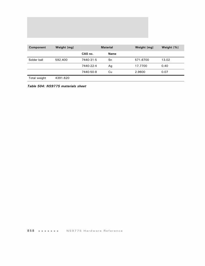
8 5 8 NS9775 Ha r dwa r e Re f e r ence
CAS no. Name
Solder ball 592.400 7440-31-5 Sn 571.6700 13.02
7440-22-4 Ag 17.7700 0.40
7440-50-8 Cu 2.9600 0.07
Total weight 4391.620
Component Weight [mg] Material Weight [mg] Weight [%]
Table 504: NS9775 materials sheet
Index
I - I n d e x - 1
Numerics10/100 Ethernet MAC 41284 parallel peripheral port 616-bit byte gap counter 705, 70616-bit maximum buffer counter 705, 70616-bit Thumb instruction set 52, 5432-bit ARM instruction set 52, 548-bit Java instruction set 54
Aabsolute maximum ratings 804access sequencing and memory width,
dynamic memory controller 235access sequencing and memory width,
static memory controller 195Active Interrupt Level Status register 173address connectivity 222address decoding 128address manipulation, ARM926EJ-S 55address mapping 236-274address translation, MMU 85-99AHB address decoding and translation 420AHB Arbiter Gen Configuration
register 149AHB behavior with noncacheable
instruction fetches 116AHB bus arbiter timeout 123, 127AHB Bus Arbiter Timeout Period
register 151AHB bus error interrupt 421AHB bus error monitoring 127AHB bus monitor timeout 127AHB Bus Monitor Timeout Period
register 151AHB Error Monitoring Configuration
register 155AHB Error Status 1 register 152AHB Error Status 2 register 153AHB input clock, LCD 577AHB interface, LCD 580-590
dual DMA FIFOs amd associated control logic 580
external pad interface signals 587generating interrupts 587grayscaler 586LCD panel signal multiplexing
details 587master and slave interfaces 580panel clock generator 586pixel serializer 581RAM palette 585timing controller 586
I n d e x - 2
upper and lower panel formatters 586AHB master interface 417AHB max burst detect 127AHB slave error response detect 127AHB slave/target interface 418alignment faults 105ambient temperatures 8arbitration and multiplexing, BBus
bridge 480ARM boot configuration (SPI-EEPROM) 498ARM debug architecture 52ARM Wake-up register 553ARM926EJ-S processor 51
about 52cache format 114DSP 82Jazelle (Java) 81Memory Management Unit. See MMU.system register addresses 55
ARM926EJ-S RISC processor 2asynchronous mode 16attributes, system control module 137-
143
BBack-to-Back Inter-Packet_Gap
register 364bandwidth requirements 495BBus
master and slave modules 484BBus bridge 479-512
arbitration (masters and slaves) 484arbitration and multiplexing 480bandwidth requirements 495BBus Bridge Interrupt Enable
register 510BBus Bridge Interrupt Status
register 509Buffer Descriptor Pointer register 502Control and Status registers 501-512control logic 481, 484-485descriptor list processing 488DMA accesses 483DMA buffer descriptor 486DMA Channel 1/2 Control register 503DMA memory-to-peripheral
transfers 483DMA Peripheral Chip Select
register 508DMA peripheral-to-memory
transfers 483DMA Status and Interrupt Enable
register 506functions 480interrupt aggregation 495main function 479peripheral address map 485register addresses 501SDRAM boot algorithm 500SPI-EEPROM boot logic 496-501SPI-EEPROM boot logic, memory
controller configuration 497system boot engine 480two-channel DMA controller 480,
486-495BBus bridge arbitration
cycles 485masters and slaves 484
BBus Bridge Control and Status registers 501-512
BBus Bridge Interrupt Enable register 510BBus Bridge Interrupt Status register 509BBus DMA controller 513-531
about the controllers 514controller block 515DMA buffer descriptor 516-521
I - I n d e x - 3
DMA Buffer Descriptor Pointer register 525
DMA channel assignments 521-522DMA context memory 515DMA Control register 526DMA Status/Interrupt Enable
register 528DMA transfer status 519-521fly-by DMA transfers 514fly-by mode 514register addresses 523
BBus DMA field 553BBus DMA Interrupt Enable register 549BBus DMA Interrupt Status register 548BBus Monitor register 547BBus peripheral address map 485BBus slave and DMA interface
module 693-721CPU mode 693DMA mode 693register map 693
BBus subsystem 513BBus utility 533-554
ARM Wake-up register 553BBus DMA Interrupt Enable
register 549BBus DMA Interrupt Status register 548BBus Monitor register 547Endian Configuration register 551GPIO Configuration register
options 540GPIO Configuration registers 535-541GPIO Control registers 541-544GPIO Status registers 544-547Master Reset register 535register addresses 534USB Configuration register 550
BGA layout 856
bist_en_n truth/termination table 31bit-rate examples 641-643bit-rate generator 615, 657
clock sources 616, 657bootstrap initialization 139-143
configuration pins 140BRC channel assignment 150BRC0, BRC1, BRC2, BRC3 registers 150BRF field 122Bridge Configuration registers 425-431Buffer Descriptor Pointer register 502Buffer Full Status register 719buffer length 487, 517buffer length bit, Ethernet 337buffer length, Ethernet 339buffer pointer, Ethernet 336, 338bus arbitration
I2C 559bus interconnection, system control
module 120bus turnaround 215-220byte lane control 221byte lane control and databus
steering 227-235little and big endian, address not right-
justified 234little and big endian, address right-
justified 227byte mode 688
data transfer cycle 688
Ccaches and write buffer 109-115
cache features 109cache MVA and set/way formats 113enabling the caches 111write buffer 110
I n d e x - 4
CAM controller 343CardBus adapter requirements 478CardBus Miscellaneous Support
register 454CardBus port 4CardBus signals 476CardBus Socket Control register 467CardBus Socket Event register 459CardBus Socket Force Event register 464CardBus Socket Mask register 460CardBus Socket Present State register 461CardBus support 474-478Carry Register 1 389Carry Register 1 Mask register 391Carry Register 2 390Carry Register 2 Mask register 393Centronics mode. See compatibility
mode.</Emphasis>chip select 1 memory configuration 191CLD signal 45Clock Configuration register 165clock frequency settings 14clock generation/system pins 30clock generator 8clock timing 849-851clocks, LCD 577coarse page tables 88, 91, 94, 96Collision Window/Retry register 366combined transmit and receive statistics
counters 379Command Transmit Data register 560compatibility mode 687
data transfer cycle 687Configuration Address Data Port
register 423Configuration Address Port register 423Configuration register 564Configuration register, memory 281
configuring the NS9775 for CardBus support 476
context (static) RAM 514control in packets 727control logic, BBus bridge 481, 484-485Control register, memory 278conventions, documentation xxiiiCore Phase (IEEE 1284) register 720CPU 51-118
about the ARM926EJ-S processor 52accessing the CP15 registers 56caches and write buffer 109-115core 51DSP 82Jazelle (Java) 81MMU 82-109
access permissions and domains 83address translation 85-99coarse page table descriptor 91disabling 108enabling 107external aborts 106fault checking sequence 103features 82fine page table descriptor 92first-level descriptor 88first-level fetch 88MMU faults and aborts 99-102program accessible registers 84second-level descriptor 93section descriptor 90subpages 99TLB structure 108translated entries 83translating parge page
references 95translating section references 93translating small page
I - I n d e x - 5
references 97translating tiny page
references 98translation table base 86
noncacheable instruction fetches 115R0, ID code and cache type status
registers 59-61R1, Control register 62-64R10, TLB Lockdown register 77R11 register 78R12 register 78R13, Process ID register 79-81R14 register 81R15, Test and debug register 81R2, Translation Table Base register 65R3, Domain Access Control
register 65, 102R4 register 66R5, Fault Status registers 66R6, Fault Address register 68, 101R7, Cache Operations register 68-72R8, TLB Operations register 72R9, Cache Lockdown register 74-77system control processor
registers 55-81addresses 55summary 57terms and abbreviations 56
CPU arbiter, high speed 121CPU bus arbitration 484CPU subsystem 121cross-bridge transaction error
handling 419
Ddata and command FIFOs 691data structures in LCD panels 582-584
DC electrical characteristics 806-807inputs 806outputs 807
DC electrical inputs, USB 806DC electrical outputs, USB 807DCache, data cache 60, 72, 109, 110, 111,
112write buffer 110
debug mode (GPTC) 131decoding. See BBus peripheral address
map.destination address 487, 517device block, USB 724, 725, 726-728
architecture 726control and status 726logical and physical endpoints 728packet and data flow 727
Device Control and Status register 734Device IP Programming Control/Status
register 740device selection for configuration,
PCI 471DMA
BBus controller. See BBus DMA controller.
descriptor list processing 488DMA accesses, BBus bridge 483
memory-to-peripheral transfers 483peripheral-to-memory transfers 483
DMA buffer descriptor 486, 516-521buffer length 517definition 517destination address 517DMA transfer status 519-521FULL bit 518illustration 517interrupt bit 518LAST bit 518
I n d e x - 6
source address 517status field 518WRAP bit 518
DMA Buffer Descriptor Pointer register 525
DMA Channel 1/2 Control register 503DMA channel assignments 521-522DMA context memory 515DMA Control register 526DMA controller
two-channel 480, 486-495initiating a DMA transfer 486
DMA memory-to-peripheral transfers 483DMA Peripheral Chip Select register 508DMA peripheral-to-memory transfers 483DMA read. See also DMA memory-to-
peripheral transfers. 483DMA Status and Interrupt Enable
register 506DMA Status/Interrupt Enable register 528DMA system 6DMA transfer
executing 486two-channel transfer
external-peripheral-initiated 486processor-initated 486
DMA transfer status 519-521DMA write. See also DMA peripheral-to-
memory transfers. 483documentation
conventions xxiiirelated xxiii
domain faults 105downstream port (USB) 724downstream transactions 417DSP 82dummy default master 123dynamc memory controller
address mapping 236-274Dynamic Memory Active Bank A to Active
Bank B Time register 295Dynamic Memory Active to Active
Command Period register 292Dynamic Memory Active to Precharge
Command Period register 287Dynamic Memory Auto refresh Period
register 293Dynamic Memory Configuration 0-3
registers 298address mapping 299
Dynamic Memory Control register 282dynamic memory controller 235-274
write protection 235dynamic memory controller, access
sequencing and memory width 235Dynamic Memory Data-in to Active
Command Time register 290Dynamic Memory Exit Self-refresh
register 294Dynamic Memory Last Data Out to Active
Time register 289Dynamic Memory Load Mode register to
Active Command Time register 296
Dynamic Memory Precharge Command Period register 286
Dynamic Memory RAS and CAS Delay 0-3 registers 302
Dynamic Memory Read Configuration register 285
Dynamic Memory Refresh Timer register 283
Dynamic Memory Self-refresh Exit Time register 288
Dynamic Memory Write Recovery Time register 291
I - I n d e x - 7
EECP mode 689-690
forward transfer cycles 689host processing sequence
example 690reverse transfer cycles 690
electrical characteristics 804electrical specifications. See Timing.ENABLE bit, Ethernet 336enable/disable interrupts for BBus
DMA 549Endian configuration 423Endian Configuration register 551Endpoint Descriptor 0-11 registers 783Ethernet communication module 325-413
Back-to-Back Inter-Packet-Gap register 364
Collision Window/Retry register 366control and status registers 346-408definition 325diagram 326Ethernet front-end (EFE) module. See
also Ethernet front-end module. 333-343
Ethernet front-end features 326Ethernet front-end module 325Ethernet General Control Register
#1 348Ethernet General Control Register
#2 352Ethernet General Status register 354Ethernet Interrupt Enable register 398Ethernet Interrupt Status register 396Ethernet MAC 327-332Ethernet MAC features 326Ethernet Receive Status register 358Ethernet timing diagrams 825-827Ethernet Transmit Status register 354
external CAM filtering 343-346General Statistics registers 388
Carry Register 1 389Carry Register 1 Mask register 391Carry Register 2 390Carry Register 2 Mask register 393
MAC Configuration Register #1 360MAC Configuration Register #2 361Maximum Frame register 367MII Management Address register 372MII Management Command
register 371MII Management Configuration
register 369MII Management Indicators
register 374MII Management Read Data
register 373MII Management Write Data
register 372Non Back-to-Back Inter-Packet Gap
register 365PHY Support register 368register addresses 346register hash tables 377RX A Buffer Descriptor Pointer Offset
register 403RX A Buffer Descriptor Pointer
register 394RX B Buffer Descriptor Offset
register 404RX B Buffer Descriptor Pointer
register 394RX C Buffer Descriptor Pointer Offset
register 405RX C Buffer Descriptor Pointer
register 395RX D Buffer Descriptor Pointer Offset
register 405RX D Buffer Descriptor Pointer
I n d e x - 8
register 395RX Free Buffer register 407sample hash table code 409-413Station Address Filter register 377Station Address registers 375Statistics registers 379
combined transmit and receive statistics counters 379
receive statistics counters 380transmit statistics counters 384
Transmit Buffer Descriptor Pointer Offset register 406
Transmit Recover Buffer Descriptor Pointer register 400
TX Buffer Descriptor Pointer register 400
TX buffer descriptor RAM 408TX Error Buffer Descriptor Pointer
register 401TX Stall Buffer Descriptor Pointer
register 402Ethernet front-end module
about 333Ethernet slave interface 341features 326interrupts 341power down mode 334receive packet processor 334resets 342transferring a frame to system
memory 335transmit packet processor 337transmitting a frame to the Ethernet
MAC 340Ethernet General Control Register #1 348Ethernet General Control Register #2 352Ethernet General Status register 354Ethernet interface pinout 29Ethernet Interrupt Enable register 398
Ethernet Interrupt Status register 396Ethernet MAC 325, 327-332
about 327external clocks 15features 326, 328PHY interface mappings 330station address logic (SAL) 331statistics module 331
Ethernet Media Access Controller. See Ethernet MAC.
Ethernet Receive Status register 358Ethernet slave interface 341Ethernet timing 825-827Ethernet Transmit Status register 354Extended Control register 714extended wait transfers 194Extensibility Byte Requested by Host
retgister 714extensibility byte values 692external aborts 106external CAM filtering 343-346
CAM controller 343External Interrupt 0-3 Control register 185external interrupts 8external pad interface signals 587external peripheral 6external system bus interface 3external-peripheral-initiated DMA transfer
(AHB) 486
Ffast interrupts. See FIQ interrupts.Feature Control Register A 710Feature Control Register B 711FIFO Interrupt Enable registers 793-798
FIFO Interrupt Enable 0 register 793FIFO Interrupt Enable 1 register 794
I - I n d e x - 9
FIFO Interrupt Enable 2 register 796FIFO Interrupt Enable 3 register 797
FIFO Interrupt Status registers 786-793FIFO Interrupt Status 0 register 788FIFO Interrupt Status 1 register 789FIFO Interrupt Status 2 register 790FIFO Interrupt Status 3 register 792
FIFO management 617-620, 659-662FIFO Packet Control registers 798FIFO Status and Control registers 799FIFO Status register 700filtering options, station address logic 331fine page tables 89, 92, 94, 97FIQ interrupts 134flash boot 11fly-by DMA transfers 514fly-by memory-to-peripheral
operations 517fly-by mode 514fly-by peripheral to memory
operations 517Forward Address register 719Forward Command DMA Control
register 705Forward Command FIFO Read register 702Forward Data DMA Control register 706Forward Data FIFO Read register 703four-channel video interface 2FULL bit 488, 518FULL bit, Ethernet 336, 338
Ggated timer 130GEN ID register 184general purpose I/O. See also GPIO.general purpose timers and counters 7general purpose timers/counters 130
General Statistics registers (Ethernet) 388Carry Register 1 389Carry Register 1 Mask register 391Carry Register 2 390Carry Register 2 Mask register 393
generating interrupts, LCD 587Global Control and Status register 733Global Interrupt Enable register 736Global Interrupt Status register 738GPIO Configuration register options 540GPIO Configuration registers 535-541GPIO Control registers 541-544GPIO MUX pinout 38GPIO Status registers 544-547GPTC. See general purpose timers/
counters.Granularity Count register 718grayscaler 586
Hhandling USB-IN packet errors 731handling USB-OUT packet errors 731Harvard-cached architecture 52HcBulkCurrentED register 761HcBulkHeadED register 760HcCommandStatus register 747HcControl register 743HcControlCurrentED register 759HcControlHeadED register 758HcDoneHead register 763HcFmInterval register 764HcFmNumber register 766HcFmRemaining register 765HcHCCA register 756HcInterruptDisable register 754HcInterruptEnable register 752
I n d e x - 10
HcInterruptStatus register 750HcLsThreshold register 768HcPeriodCurrentED register 757HcPeriodicStart register 767HCRevision register 743HcRhDescriptorA register 770HcRhDescriptorB register 772HcRhPortStatus1 register 776HcRhStatus register 773high-speed bus architecture 121high-speed peripheral subsystem 121horizontal axis panel 591horizontal timing restrictions,
LCDTiming0 593host block, USB 724, 726, 728-730
control and status 728packet data flow 729
hsel_x signal 128
II bit, Ethernet 336, 338I2C
bus arbitration 559command interface 557Command Transmit Data register 560Configuration register 564external addresses 557locked interrupt driven mode 558Master Address register 562master module commands 558master module flowchart 568master software driver 567master/slave interface 555-569module 556physical bus 556register addresses 559
Slave Address register 563slave module commands 558slave module flowchart 569Status Receive Data register 561timing diagram 833
I2C controllerport features 6
I2C pinout 47I2C timing 833ICache, instruction cache 55, 60, 109, 111IDLE condition 617IEEE 1284
BBus slave and DMA interface module 693-721
Buffer Full Status register 719byte mode 688compatibility mode 687Core Phase (IEEE 1284) register 720data and command FIFOs 691ECP mode 689-690Extended Control register 714Extensibility Byte Requested by Host
register 714extensibility byte values 692Feature Control Register A 710Feature Control Register B 711FIFO Status register 700Forward Address register 719Forward Command DMA Control
register 705Forward Command FIFO Read
register 702Forward Data DMA Control
register 706Forward Data FIFO Read register 703General Configuration register 695Granularity Count register 718Interrupt Enable register 711
I - I n d e x - 1 1
Interrupt Status and Control register 697
Interrupt Status register 715Interrupt Timeout Counter
register 716Master Enable register 713negotiation 692nibble mode 688peripheral controller 685-721peripheral port control module 686Pin Interrupt Control register 717Pin Interrupt Mask register 716Port Control register 709Port Status register, host 708Port Status register, peripheral 710Printer Data Pins register 707register map (BBus slave and DMA
interface) 693requirements 686Reverse FIFO Write register 703Reverse FIFO Write Register - Last 703timing diagram 843
IEEE 1284 General Configuration register 695
IEEE 1284 timing 843individual interrupts, LCD 578industry-standard Ethernet interfaces
MII 325RMII 325
initializing PLL parameters 15initiating a DMA transfer, two channel
(AHB) 486Int Config registers (0-31) 158
register address mapping 158interrupt aggregation 495INTERRUPT bit 488interrupt bit 518interrupt codes 565
Interrupt Configuration register 134interrupt controller 134-137
FIQ interrupts 134interrupt sources 135, 136IRQ interrupts 134vector interrupt controller 137
Interrupt Enable register 711interrupt sources 135, 136Interrupt Status Active register 161Interrupt Status and Control register 697interrupt status bits for DMA 548Interrupt Status Raw register 162Interrupt Status register 715Interrupt Timeout Counter register 716Interrupt Vector Address register 134Interrupt Vector Address Register Level 0-
31 157interrupts
CardBus 478Ethernet 341PCI 421, 472
interrupts, LCD 611-612master bus error interrupt 611next base address update
interrupt 612vertical compare interrupt 611
IRQ interrupts 134IRSADDR register 160
JJazelle (Java) 81JBIG 2JTAG interface
pinout for ARM core/boundary scan 47JTAG timing 848
I n d e x - 12
LL bit, Ethernet 338LAST bit 488, 518LCD controller 45, 571-612
about 571AHB interface 580-590
dual DMA FIFOS and associated control logic 580
external pad interface signals 587generating interrupts 587grayscaler 586LCD panel signal multiplexing
details 587master and slave interfaces 580panel clock generator 586pixel serializer 581RAM palette 585timing controller 586upper and lower panel
formatters 586clocks 577color STN panels 574features 5, 572-576functional overview 576-579interrupts 611-612
master bus error interrupt 611next base update interrupt 612vertical compare interrupt 611
LCD panel resolution 573LCD timing diagrams 834-838LCDControl register 602LCDInterrupt register 606LCDINTRENABLE register 601LCDLPBASE register 599LCDLPCURR register 607LCDPalette register 608LCDStatus register 605LCDTiming0 register 591
LCDTiming1 register 594LCDTiming2 register 596
panel clock divider restrictions 598
LCDTiming3 register 599LCDUPBASE register 599LCDUPCURR register 607mono STN panels 575number of colors 574panel support 573power up/power down sequence 575programmable parameters 572register addresses 591registers 591-610signals and interrupts 578
individual interrupts 578programmable control signals 578single combined interrupt 578
supported display types 576TFT panels 574
LCD input clock 577LCD module signals 45LCD panel resolution 573LCD panel signal multiplexing details 587LCD panel support 573LCD timing 834-838LCDControl register 602LCDInterrupt register 606LCDINTRENABLE register 601LCDLPBASE register 599LCDLPCURR register 607LCDPalette register 608
big endian configuration 608little endian configuration 608
LCDStatus register 605LCDTiming0 register 591
horizontral timing restriction 593LCDTiming1 register 594
I - I n d e x - 1 3
LCDTiming2 register 596panel clock divider restrictions 598
LCDTiming3 register 599LCDUPBASE register 599LCDUPCURR register 607locked bus sequence 123locked interrupt driven mode 558low-power operation 190low-power SDRAM deep-sleep mode 190low-power SDRAM partial array
refresh 190
MMAC Configuration Register #1 360MAC Configuration Register #2 361main arbiter, high speed 122Master Address register 562master bus error interrupt
(MBERRORINTR) 611Master Enable register 713master module commands, I2C 558Master Reset register 535master reset. See reset function.maximum clock rates
NS9775 16Maximum Frame register 367maximum power dissipation 805Media Independent Interface. See MII.memory controller 187-312
access sequencing and memory width, dynamic memory controller 235
access sequencing and memory width, static memory controller 195
address connectivity 222address mapping, dynamic memory
controller 236-274
bootstrap signals 191bootstrap signals, memory
controller 191bus turnaround 215-220byte lane control 221byte lane control and databus
steering 227-235Configuration register 281configuration, SPI-EEPROM 497Control register 278Dynamic Memory Active Bank A to
Active Bank B Time register 295
Dynamic Memory Active to Active Command Period register 292
Dynamic Memory Active to Precharge Command Period register 287
Dynamic Memory Auto Refresh Period register 293
Dynamic Memory Configuration 0-3 registers 298
address mapping 299Dynamic Memory Control register 282dynamic memory controller 235-274Dynamic Memory Data-in to Active
Command Time register 290Dynamic Memory Exit Self-refresh
register 294Dynamic Memory Last Data Out to
Active Time register 289Dynamic Memory Load Mode register
to Active Command Time register 296
Dynamic Memory Precharge Command Period register 286
Dynamic Memory RAS and CAS Delay 0-3 registers 302
Dynamic Memory Read Configuration register 285
Dynamic Memory Refresh Timer
I n d e x - 14
register 283Dynamic Memory Self-refresh Exit
Timer register 288Dynamic Memory Write Recovery Time
register 291extended wait transfers 194features 188low-power operation 190memory map 190memory mapped peripherals 194memory timing diagrams 809-824register addresses 275registers 275-312Static Memory Configuration 0-3
registers 303static memory controller 192-235static memory controller
configurations 193static memory controller
initialization 194-220Static Memory Extended Wait
register 297Static Memory Output Enable Delay 0-
3 registers 308Static Memory Page Mode Read Delay
0-3 registers 310static memory read control 196-208Static Memory Turn Round Delay 0-3
registers 312static memory write control 208-215Static Memory Write Delay 0-3
registers 311Static Memory Write Enable Delay 0-3
registers 307Status register 280system overview 189write protection
dynamic memory controller 235static memory controller 193
Memory Management Unit. See MMU.memory map 190memory mapped peripherals 194memory timing 809-824MII 325MII Management Address register 372MII Management Command register 371MII Management Configuration
register 369clocks field settings 370
MII Management Indicators register 374MII Management Read Data register 373MII Management Write Data register 372Miscellaneous System Configuration and
Status register 169MMU 82-109
access permissions and domains 83address translation 85-99coarse page table descriptor 91disabling 108domain access control 102enabling 107external aborts 106fault checking sequence 103
alignment faults 105domain faults 105permission faults 106translation faults 105
features 82fine page table descriptor 92first-level descriptor 88first-level fetch 88MMU faults and aborts 99-102program accessible registers 84second-level descriptor 93section descriptor 90subpages 99TLB structure 108
I - I n d e x - 1 5
translated entries 83translating large page references 95translating section references 93translating small page references 97translating tiny page references 98translation table base 86
Nnegotiation, IEEE 1284 692next base address update interrupt
(LNBU) 612nibble mode 688
data transfer cycle 688Non Back-to-Back Inter-Packet-Gap
register 365noncacheable instruction fetches 115
AHB behavior 116NS9750
10/100 Ethernet MAC 41284 parallel peripheral port 6clock generation/system pins
pinout 30clock generator 8definition 1DMA 6Ethernet interface pinout 29external interrupts 8external peripheral 6external system bus interface 3features 2-8general purpose I/O (GPIO) 7general purpose timers and counters 7GPIO MUX 38I2C pinout 47I2C port 6JTAG interface pinout 47LCD controller 5
LCD module signals 45operating grades and ambient
temperatures 8PCI CardBus port 4PCI pinout 32PCI/CardBus signals 35peripheral bus 6pinout 22-49power ground 49power management 7processor 2reserved pins 49reset function 11-14serial ports 5software resets 13system boot 4system bus 6system clock 14system memory interface pinout 22system memory interface signals 26system timers 7system-level interfaces 9USB clock 18USB interface pinout 47USB ports 5vector interrupt controller 7
NS9775about 21configuring for CardBus support 476definition 1, 2four channel video interface 2maximum clock rates 16print engine controller 2printer engine interface pinout 45printer video clock 16
I n d e x - 16
Ooperating grades 8
Ppackaging 853-858
BGA layout 856dimensions 854-855
PAD operation table 364panel clock generator 586PCI
CardBus port 4interface pinout 32PCI/CardBus signals 35
PCI address decoding and mapping 421PCI Arbiter Configuration register 435PCI Arbiter Interrupt Enable register 437PCI Arbiter Interrupt Status register 436PCI arbiter. See PCI bus arbiter.PCI Base Address registers 429PCI BIST register 429PCI Bridge Address Translation Control
register 453PCI Bridge AHB Error Address register 445PCI Bridge AHB to PCI Memory Address
Translate 0 register 449PCI Bridge AHB to PCI Memory Address
Translate 1 register 450PCI Bridge AHB-to-PCI IO Address Translate
register 451PCI Bridge Configuration register 444PCI Bridge Interrupt Enable register 447PCI Bridge Interrupt Status register 446PCI Bridge PCI Error Address register 446PCI Bridge PCI to AHB Memory Address
Translate 0 register 451PCI Bridge PCI to AHB Memory Address
Translate 1 register 452
PCI burst read from NS9775 timing 831PCI burst read to NS9775 timing 832PCI burst write from NS9775 timing 830PCI burst write to NS9775 timing 831PCI bus arbiter 419, 431-468
about 431configuration registers 433-468functional description 431register addresses 433slave interface 433
PCI bus error interrupt 421PCI Cache Size register 429PCI CardBus CIS Pointer register 430PCI central resource functions 472PCI Class Code register 429PCI Command register 426PCI Configuration 0 register 441PCI Configuration 1 register 441PCI Configuration 2 register 442PCI Configuration 3 register 443PCI Device ID register 426PCI Expansion ROM register 430PCI Header register 429PCI Interrupt Line register 430PCI Interrupt Pin register 430PCI Latency Timer register 429PCI master interface 418PCI Max Latensy register 431PCI Min Grant register 431PCI Miscellaneous Support register 438PCI Revision ID register 428PCI Status register 427PCI Subsystem ID register 430PCI Subsystem Vendor ID register 430PCI system configurations 469-474
central resource functions 472device selection 471interrupts 472
I - I n d e x - 1 7
PCI target error filtering 420PCI target interface 418PCI timing 828-832
PCI burst read from NS9775 timing 831PCI burst read to NS9775 timing 832PCI burst write from NS9775
timing 830PCI burst write to NS9775 timing 831
PCI Vendor ID register 426PCI-to-AHB bridge 415-478
AHB address decoding and translation 420
AHB master interface 417AHB slave/target interface 418Bridge Configuration registers 425-
431CardBus adapter requirements 478CardBus Miscellaneous Support
register 454CardBus Socket Control register 467CardBus Socket Event register 459CardBus Socket Force Event
register 464CardBus Socket Mask register 460CardBus Socket Present State
register 461CardBus support 474-478central resource functions 472Configuration Address Data Port
register 423Configuration Address Port
register 423configuration and status registers 418configuration registers 423configuring the NS9775 for CardBus
suppport 476definition 415device selection for configuration 471Endian configuration 423
features 416functionality 417-419interrupts 421, 472PCI address decoding and mapping 421PCI Arbiter Configuration register 435PCI Arbiter Interrupt Enable
register 437PCI Arbiter Interrupt Status
register 436PCI Base Address registers 429PCI BIST register 429PCI Bridge Address Translation Control
register 453PCI Bridge AHB Error Address
register 445PCI Bridge AHB to PCI Memory Address
Translate 0 register 449PCI Bridge AHB to PCI Memory Address
Translate 1 register 450PCI Bridge AHB-to-PCI IO Address
Translate register 451PCI Bridge Configuration register 444PCI Bridge Interrupt Enable
register 447PCI Bridge Interrupt Status
register 446PCI Bridge PCI Error Address
register 446PCI Bridge PCI to AHB Memory Address
Translate 0 register 451PCI Bridge PCI to AHB Memory Address
Translate 1 register 452PCI bus arbiter 419, 431-468
configuration registers 433-468register addresses 433slave interface 433
PCI Cache Size register 429PCI CardBus CIS Pointer register 430PCI Class Code register 429
I n d e x - 18
PCI Command register 426PCI Configuration 0 register 441PCI Configuration 1 register 441PCI Configuration 2 register 442PCI Configuration 3 register 443PCI Device ID register 426PCI Expansion ROM register 430PCI Header register 429PCI Interrupt Line register 430PCI Interrupt Pin register 430PCI Latency Timer register 429PCI Max Latency register 431PCI Min Grant register 431PCI Miscellaneous Support register 438PCI Revision ID register 428PCI Status register 427PCI Subsystem register 430PCI Subsystem Vendor ID register 430PCI target error filtering 420PCI target interface 418PCI timing diagrams 828-832PCI Vendor ID register 426register addresses, PCI/bridge
configuration 425system configurations 469-474transaction ordering 423
PCI-to-AHB busCardBus interrupts 478PCI master interface 418
PCI-to-AHB-bridgePCI bus arbiter
functional description 431peripheral bus 6peripheral DMA read access 489peripheral DMA write access 490peripheral REQ and DONE signalling 491permission faults 106PHY Support register 368
Pin Interrupt Control register 717Pin Interrupt Mask register 716pinout
clock generation/system pins 30Ethernet interface 29GPIO MUX 38I2C 47JTAG interface 47NS9750 22-49PCI interface 32printer engine interface 45reserved pins 49system memory interface 22USB interface 47
pixel serializer 581PLL configuration 138PLL Configuration register 171PLL multiplier values 141pll_test_n truth/termination table 31Port Control register 709Port Status register, host 708Port Status register, peripheral 710power down mode, Ethernet 334power ground 49power management 7power sequencing 808power up/power down sequence, LCD 575power-on reset memory map 190print engine clock
example 18print engine controller 2Printer Data Pins register 707printer engine interface pinout 45printer video clock 16
synchronous mode 16priority encoder block 135privileged access mode 129processor-initiated DMA transfer
I - I n d e x - 1 9
(AHB) 486programmable control signals, LCD 578programmable parameters, LCD 572programmable timers 130-131
general purpose timers/counters 130software watchdog timer 130
RR0, ID code and cache type status
registers 59-61R1, Control register 62-64R10, TLB Lockdown register 77R11 register 78R12 register 78R13, Process ID register 79-81R14 register 81R15, Test and debug register 81R2, Translation Table Base register 65R3, Domain Access Control register 65,
102R4 register 66R5, Fault Status registers 66R6, Fault Address register 68, 101R7, Cache Operations register 68-72R8, TLB Operations register 72R9, Cache Lockdown register 74-77RAM palette 585raw interrupt status 605receive alignment error counter 382receive broadcast packet counter 381receive buffer descriptor format
Ethernet 336receive byte counter 380receive carrier sense error counter 383receive code error counter 382receive control frame packet counter 382receive FCS error counter 381
receive FIFO interface 618, 660receive fragments counter 383receive jabber counter 383receive multicast packet counter 381receive oversize packet counter 383receive packet counter 381receive packet processor 333, 334receive PAUSE frame packet counter 382receive statistics counters (Ethernet) 380receive undersize packet counter 383receive unknown OPCODE packet
counter 382recommended operating conditions 804Reduced Media Independent Interface.
See RMII.register hash tables 377regular timer 130related documentation xxiiirelinquishing the bus 123reserved pins 49Reset and hardware strapping timing 847Reset and Sleep Control register 167reset function
boot sequence 12master reset 11RESET DONE as input 12RESET DONE as output 12
reset values 277resets, Ethernet 342Reverse FIFO Write register 703Reverse FIFO Write Register - Last 703RMII 325root hub, USB 769RX A Buffer Descriptor Pointer Offset
register 403RX A Buffer Descriptor Pointer
register 394RX B Buffer Descriptor Pointer Offset
I n d e x - 20
register 404RX B Buffer Descriptor Pointer
retgister 394RX C Buffer Descriptor Pointer Offset
register 405RX C Buffer Descriptor Pointer
register 395RX D Buffer Descriptor Pointer Offset
register 405RX D Buffer Descriptor Pointer
register 395RX Free Buffer register 407
Ssample hash table code 409-413scan_en_n truth/termination table 31SDRAM boot algorithm 500self-refresh mode 190Serial Channel B/A/C/D Bit-rate
register 637, 674Serial Channel B/A/C/D Control Register
A 623, 664Serial Channel B/A/C/D Control Register
B 627, 667Serial Channel B/A/C/D FIFO Data
register 644, 679Serial Channel B/A/C/D Flow Control
Force register 652Serial Channel B/A/C/D Flow Control
register 650Serial Channel B/A/C/D Receive Buffer
GAP Timer register 645, 680Serial Channel B/A/C/D Receive Character
GAP Timer register 646, 681Serial Channel B/A/C/D Receive Match
MASK register 684Serial Channel B/A/C/D Receive Match
register 648, 683
Serial Channel B/A/C/D Recieve Match MASK register 649
Serial Channel B/A/C/D Status Register A 630, 669
serial controllerport features 5UART features 5
serial controller, SPI 655-684bit-rate generator 657features 656FIFO management 659-662receive FIFO interface 660Serial Channel B/A/C/D Bit-rate
register 674Serial Channel B/A/C/D Control
Register A 664Serial Channel B/A/C/D Control
register B 667Serial Channel B/A/C/D FIFO Data
register 679Serial Channel B/A/C/D Receive Buffer
GAP Timer register 680Serial Channel B/A/C/D Receive
Character GAP Timer register 681
Serial Channel B/A/C/D Receive Match MASK register 684
Serial Channel B/A/C/D Receive Match register 683
Serial Channel Status Register A 669serial port control and status
registers 662-684serial port performance 662SPI timing diagrams 839-842structure 656transmit FIFO interface 659
serial controller, UART 613-653bit-rate examples 641-643bit-rate generator 615
I - I n d e x - 2 1
features 614FIFO management 617-620
receive FIFO interface 618transmit FIFO interface 617
framing structure 616functions 617Serial Channel B/A/C/D Bit-rate
register 637Serial Channel B/A/C/D Control
Register A 623Serial Channel B/A/C/D Control
Register B 627Serial Channel B/A/C/D FIFO Data
register 644Serial Channel B/A/C/D Flow Control
Force register 652Serial Channel B/A/C/D Flow Control
register 650Serial Channel B/A/C/D Receive Buffer
GAP Timer register 645Serial Channel B/A/C/D Receive
Character GAP Timer register 646
Serial Channel B/A/C/D Receive Match MASK register 649
Serial Channel B/A/C/D Receive Match register 648
Serial Channel B/A/C/D Status Register A 630
serial port control and status registers 620-653
serial port performance 620serial EEPROM boot 11Serial Interface Engine 729serial port control and status
registers 620-653, 662-684SPI register addresses, serial
controllers B and A 662SPI register addresses, serial
controllers C and D 663
UART register addresses, serial controllers B and A 620
UART register addresses, serial controllers C and D 621
serial port maximum rates, UART 620serial port performance 620, 662SHOULD BE ONE, SBO (CP15 registers) 57SHOULD BE ZERO or PRESERVED, SBZP
(CP15 registers) 57SHOULD BE ZERO, SBZ (CP15 registers) 57signals
external pad interface 587LCD module 45PCI/CardBus 35system memory interface 26
signals and interrupts, LCD 578single combined interrupt 578Slave Address register 563slave module commands, I2C 558slew rates, USB PHY 728Software Watchdog Configuration
register 163software watchdog timer 130Software Watchdog Timer register 165source address 487, 517SPI mode 658
individual mode definition 659individual modes 658See also serial controller, SPI.
SPI timing 839-842SPI-EEPROM boot logic 496-501
ARM (memory) boot configuration 498example 496memory controller configuration 497
spike filter 564SPLIT transfers 124state machine 514static (context) RAM 514
I n d e x - 22
Static Memory Configuration 0-3 registers 303
static memory controller 192-235configurations 193extended wait transfers 194initialization 194-220memory mapped peripherals 194write protection 193
static memory controller, access sequencing and memory width 195
Static Memory Extended Wait register 297static memory initialization 194-220
bus turnaround 215-220static memory read control 196-208static memory write control 208-215wait state generation 195
Static Memory Output Enable Delay (0-3) registers 308
Static Memory Page Mode Read Delay 0-3 registers 310
static memory read control 196-208Static Memory Turn round Delay 0-3
registers 312static memory write control 208-215Static Memory Write Delay 0-3
registers 311Static Memory Write Enable Delay 0-3
registers 307Station Address Filter register 377station address logic (SAL) 331Station Address registers 375statistics module 331Statistics registers (Ethernet) 379
combined transmit and receive statistics counters 379
receive statistics counters 380transmit statistics counters 384
status bit, Ethernet 336, 338status field 518
Status Receive Data register 561Status register, memory 280STN display panels 576STN displays 577synchronization logic 580synchronous mode 16system address map 128system boot
BBus bridge function 480system bus 6system bus arbiter 120-126
configuration examples 124CPU arbiter, high-speed 121CPU subsystem 121locked bus sequence 123main arbiter, high-speed 122ownership 123procedure 122relinquishing the bus 123SPLIT transfers 124
system clock 14system clock generation, PLL 139system configuration registers 143-185
register addresses 143system control module 119-185
Active Interrupt Level Status register 173
address decoding 128AHB Arbiter Gen Configuration
register 149AHB Bus Arbiter Timeout Period
register 151AHB bus error monitoring 127AHB Bus Monitor Timeout Period
register 151AHB Error Monitoring Configuration
register 155AHB Error Status 1 register 152
I - I n d e x - 2 3
AHB Error Status 2 register 153bootstrap initialization 139-143BRC channel assignment 150BRC0, BRC1, BRC2, BRC3 registers 150bus arbiter configuration
examples 124bus interconnection 120Clock Configuration register 165definition 119External Interrupt 0-3 Control
register 185features 120Gen ID register 184general purpose timers/counters 130Int Config registers (0-31) 158
register address mapping 158interrupt controller 134-137Interrupt Status Active register 161Interrupt Status Raw register 162Interrupt Vector Address Register
Level 0-31 157ISRADDR register 160Miscellaneous System Configuration
and Status register 169PLL configuration 138PLL Configuration register 171programmable timers 130-131register addresses 143Reset and Sleep Control register 167Software Watchdog Configuration
register 163software watchdog timer 130Software Watchdog Timer register 165SPLIT transfers 124system address map 128system attributes 137-143system bus arbiter 120-126
high-speed peripheral subsystem 121
system configuration registers 143-185
System Memory Chip Select 0 Dynamic Memory Base and Mask registers 176
System Memory Chip Select 0 Static Memory Base and Mask registers 180
System Memory Chip Select 1 Dynamic Memory Base and Mask registers 177
System Memory Chip Select 1 Static Memory Base and Mask registers 181
System Memory Chip Select 2 Static Memory Base and Mask registers 182
System Memory Chip Select 3 Dynamic Memory Base and Mask registers 179
System Memory Chip Select 3 Static Memory Base and Mask registers 183
System Memory Chip Select 6 Dynamic Memory Base and Mask registers 178
Timer 0-15 Control registers 174Timer 0-15 Read register 157Timer 0-15 Reload Count registers 156Timer Interrupt Status register 163vectored interrupt controller 137
system control module bootstrap configuration pins 140
system control processor (CP15) registers 55-81
accessing 56ARM926EJ-S system addresses 55R0, ID code and cache type status
registers 59-61R1, Control register 62-64R10, TLB Lockdown register 77
I n d e x - 24
R11 register 78R12 register 78R13, Process ID register 79-81R14 register 81R15, Test and debug register 81R2, Translation Table Base register 65R3, Domain Access Control
register 65, 102R4 register 66R5, Fault Status registers 66R6, Fault Address register 68, 101R7, Cache Operations register 68-72R8, TLB Operations register 72R9, Cache Lockdown register 74-77summary 57
System Memory Chip Select 0 Dynamic Memory Base and Mask registers 176
System Memory Chip Select 0 Static Memory Base and Mask registers 180
System Memory Chip Select 1 Dynamic Memory Base and Mask registers 177
System Memory Chip Select 1 Static Memory Base and Mask registers 181
System Memory Chip Select 2 Static Memory Base and Mask registers 182
System Memory Chip Select 3 Dynamic Memory Base and Mask registers 179
System Memory Chip Select 3 Static Memory Base and Mask registers 183
System Memory Chip Select 6 Dynamic Memory Base and Mask registers 178
system memory interface
pinout 22signals 26
system timers 7system-level interfaces 9
TTFT display panels 576TFT displays 577Timer 0-15 Control registers 174Timer 0-15 Read register 157Timer 0-15 Reload Count registers 156Timer Interrupt Status register 163timing 803-852
about 803absolute maximum ratings 804clock timing 849-851DC electrical characteristics 806-807
inputs 806outputs 807
electrical characteristics 804Ethernet timing 825-827I2C timing 833IEEE 1284 timing 843JTAG timing 848LCD timing 834-838maximum power dissipation 805memory timing 809-824PCI burst read from NS9775 831PCI burst read to NS9775 832PCI burst write from NS9775 830PCI burst write to NS9775 831PCI timing 828-832power sequencing 808recommended operating
conditions 804reset and hardware strapping 847
I - I n d e x - 2 5
SPI timing 839-842USB timing 844-846
timing controller, LCD 586TLB structure 108transaction ordering, AHB-to-PCI
bridge 423transferring a frame to system memory,
Ethernet 335translation faults 105Translation Lookaside Buffer (TLB) 82transmission error handling, USB 730transmit broadcast packet counter 385transmit buffer descriptor format
Ethernet 337Transmit Buffer Descriptor Pointer Offset
register 406transmit byte counter 385transmit deferral packet counter 385transmit excessive collision packet
counter 386transmit excessive deferral packet
counter 386transmit FCS error counter 387transmit FIFO interface 617, 659transmit fragment counter 388transmit jabber frame counter 387transmit late collision packet counter 386transmit multicast packet counter 385transmit multiple collision packet
counter 386transmit oversize frame counter 387transmit packet counter 385transmit packet processor 334, 337Transmit Recover Buffer Descriptor
Pointer register 400transmit single collision packet
counter 386transmit statistics counters 384transmit total collision packet
counter 387transmit undersize frame counter 388transmitting a frame to the Ethernet
MAC 340TX Buffer Descriptor Pointer register 400TX buffer descriptor RAM 408TX Error Buffer Descriptor Pointer
register 401TX Stall Buffer Descriptor Pointer
register 402typical power dissipation 805
UUART
features 5UART mode 616
See also serial controller, UART.UNDEFINED (CP15 registers) 57UNPREDICTABLE (CP15 registers) 57up/down counters 130upper and lower panel formatters 586upstream port (USB) 724upstream transactions 417USB clock 18USB Configuration register 550USB controller 723-802
about 724DC electrical inputs 806DC electrical outputs 807device block 726-728device block architecture 726Device Control and Status register 734device endpoint 730device endpoint status 787Device IP Programming Control/Status
register 740FIFO Interrupt Enable 0 register 793
I n d e x - 26
FIFO Interrupt Enable 1 register 794FIFO Interrupt Enable 2 register 796FIFO Interrupt Enable 3 register 797FIFO Interrupt Enable registers 793-
798FIFO Interrupt Status 0 register 788FIFO Interrupt Status 1 register 789FIFO Interrupt Status 2 register 790FIFO Interrupt Status 3 register 792FIFO Interrupt Status registers 786-
793FIFO Packet Control registers 798FIFO Status and Control registers 799Global Interrupt Enable register 736Global Interrupt Status register 738HcBulkCurrentED register 761HcBulkHeadED register 760HcCommandStatus register 747HcControl register 743HcControlCurrentED register 759HcControlHeadED register 758HcDoneHead register 763HcFmInterval register 764HcFmNumber register 766HcFmRemaining register 765HcHCCA register 756HcInterruptDisable register 754HcInterruptEnable register 752HcInterruptStatus register 750HcLsThreshold register 768HcPeriodCurrentED register 757HcPeriodicStart register 767HCRevision register 743HcRhDescriptorA register 770HcRhDescriptorB register 772HcRhPortStatus1 register 776HcRhStatus register 773host block 728-730
module architecture 724port features 5register "block" addresses 732registers 732-802
device block 782-784device block addresses 782Device Endpoint FIFO Control and
Data register addresses 784
Device Endpoint FIFO Control and Data registers 784-802
global 732-741Global Control and Status 733global register addresses 732host block 741-781host block addresses 742host block reserved bits 741host block, root hub partition
registers 769root hub 769transmission error handling 730USB timing diagrams 844-846
USB interface pinout 47USB timing 844-846
Vvector interrupt controller 7vectored interrupt controller (VIC) 137vertical axis panel 594vertical compare interrupt
(VCOMPINTR) 611
Wwait state generation 195water level marks 580WRAP bit 488, 518
I - I n d e x - 2 7
WRAP bit, Ethernet 336, 337write protection
dynamic memory controller 235static memory controller 193

2 8 NS9775 Ha r dwa r e Re f e r ence