Embed Size (px)
Citation preview

Structural and Electrical Properties of CuAlMo Thin Films Prepared by Magnetron Sputtering
Martin Birkett, Roger Penlington, Chaoying Wan & Guillaume ZoppiComputing, Engineering & Information Sciences
Northumbria University, Ellison Building, Newcastle upon Tyne, NE1 8ST
Tel: +44 191 227 3763 [email protected]
Abstract
The structure and electrical properties of a novel low resistivity CuAlMo thin film
resistor material were investigated. The thin films were grown on Al2O3 and glass
substrates by direct current (dc) magnetron sputtering. The key electrical properties
of sheet resistance, temperature coefficient of resistance (TCR) and resistance
stability were investigated as a function of sputtering pressure and post-deposition
heat treatment time and temperature. A low sputtering pressure range of 1 to 3
mTorr produced CuAlMo films with sheet resistance in the range 0.1 to 0.2 Ω/ and
resistance stability of 0.45 to 0.65% with a TCR of -90 ppm/°C which could be shifted
to zero following annealing in air at 425 °C. Films grown at higher sputtering
pressures of 4 to 6 mTorr had increased sheet resistance in the range 0.4 to 0.6
Ω/ and inferior stability of 0.8 to 1.7% with a more negative TCR of -110 to -180
ppm/°C which could not be shifted to zero following annealing. The stability of the
films grown at 1 and 3 mTorr could be further improved to <0.25% with heat
treatment, due to the formation of a protective aluminium oxide layer. A minimum
dwell time of 3 hours at 425 °C was required to stabilise the films and set the
electrical properties.
1
1
2
3456789
10
11
12
13
14
15
16
17
18
19
20
21
22
23
24
25
26
27
28

Keywords: CuAlMo, thin film resistor, dc magnetron sputtering, annealing, electrical
properties.
1. Introduction
Thin film resistors (TFR) are used extensively in electronic circuits due to their high
accuracy and excellent long term stability [1-3]. One of the most widely used TFR
materials is nickel-chromium (NiCr) which has a temperature coefficient of resistance
(TCR) of <+/-50 parts per million/°C (ppm/°C) and can cover a wide sheet resistance
range of 10 to 500 Ω/ [4] . However In recent years there has been an increase in
demand for lower value TFR in the range 0.1 to 10 Ω, especially in portable devices
for the purpose of saving battery power [5]. This requirement is difficult to meet with
NiCr due to the associated increase in film thickness, which is costly to deposit and
can also cause problems at the subsequent laser trimming stage, where it becomes
difficult to ablate.
In a bid to overcome this problem a new TFR material of copper-aluminium-
molybdenum (CuAlMo) has been developed which possess a lower resistivtiy of ~80
µΩcm yet retain electrical performance in line with the established NiCr film [6]. Thus
allowing lower resistance films to be deposited in shorter timescales with reduced
material usage.
Initial investigations have shown that electrically stable films of CuAlMo possessing
sheet resistances of <1 Ω/ can be sputtered at a pressure of 1 mTorr using a
cathode power of 1000 W [7]. Following heat treatment at 450 °C in an air
atmosphere for 5 hours the negative as-grown TCR property of the films was shifted
to near zero. The aim of this work is to further investigate the effect of sputtering and
2
1
2
3
4
5
6
7
8
9
10
11
12
13
14
15
16
17
18
19
20
21
22
23
24
25

annealing process parameters on the structural and electrical properties of the
CuAlMo films.
There have been numerous studies undertaken recently in this area [8-12]. A
reduction in sheet resistance and increase in TCR with sputtering time can be largely
attributed to increasing film thickness.
In addition to film thickness, the deposition rate is also known to influence the grain
size and the number of residual gas molecules or impurities captured within the
growing film. Increasing the deposition rate generally leads to the formation of fine
grained structures with a low concentration of impurities [13], provided the substrate
is cooled. However for un-cooled substrates, increasing the sputtering rate through
the energy of the bombarding Ar ions can in turn lead to an increase in the energy of
the ejected atoms from the sputtering target. On reaching the substrate these atoms
have a higher surface mobility, thus raising the temperature of the substrate and
resulting in a larger grained film structure [14]. Furthermore it has also been shown
that exceeding a critical deposition rate can lead to the burial of these mobile surface
atoms, there by impeding grain growth [15]. This situation can also result in an
increase in the density of vacancies captured in the film, since they have less time to
escape.
In addition to deposition rate, sputtering pressure and substrate temperature are also
known to play significant roles in determining the structure of the growing film [16].
The combined influences of substrate temperature and sputtering pressure have
been considered in a now classical article by Thornton [17].
3
1
2
3
4
5
6
7
8
9
10
11
12
13
14
15
16
17
18
19
20
21
22
23
24
25

In this model an increase in sputtering gas pressure allows more Ar atoms to be
adsorbed at the substrate surface. This limits the mobility and hence the surface
diffusion of arriving adatoms resulting in a structure with porous grain boundaries.
Conversely, an increase in substrate temperature enhances surface mobility and
conventional bulk diffusion, producing a film structure consisting of columnar grains
with fully dense boundaries.
The current study will focus specifically on the combined effect of sputtering pressure
and annealing time and temperature on the electrical performance of these new
CuAlMo films. In particular the influence of these process parameters on the
important film properties of sheet resistance, TCR and long term stability are
investigated.
4
1
2
3
4
5
6
7
8
9
10
11
12
13
14
15
16
17
18
19
20
21
22
23
24
25

2. Experimental
The films were sputtered from a CuAlMo 69/24/7 wt.% target using a Circuit
Processing Apparatus 900 (CPA) load locked deposition plant which had been
modified to give fully automatic control. All films were deposited at the previously
optimised cathode power and sputtering time of 1000 W and 24 min, respectively [7].
The sputtering pressure was varied between 1 and 6 mTorr for each experimental
run through control of the Ar gas flow rate.
Prior to each experimental run the plant was conditioned to improve accuracy. This
process involved evacuating the plant to a base pressure of 1x10 -7 Torr, before
taking a footprint analysis of the gases present in the chamber using a residual gas
analyser (RGA), type MKS e-vision Mass Spectrometer, coupled with RGA Data
Recall software. For each run this was compared to a control footprint for the plant,
to check for any abnormalities. Once the base pressure was satisfactory, the
CuAlMo target was pre-sputtered for 30 minutes under the required conditions for
that experimental run, to remove contaminations from the target surface and stabilise
the magnetron discharge parameters. No intentional substrate heating was used but
under the above conditions a maximum substrate temperature of 325°C could be
reached.
The substrate materials used were as-fired Al2O3 for electrical measurements and
borosilicate glass for structural and dimensional characterisation. Both substrate
types were 0.635 mm thick and were supplied in a standard 70 mm x 60 mm plate
form to suit automatic processing equipment.
5
1
2
3
4
5
6
7
8
9
10
11
12
13
14
15
16
17
18
19
20
21
22
23
24
25

Terminations
Resistor pattern
Substrate
I1 I2
V1 V2
I Force
V Sense
1 2 3 4 5
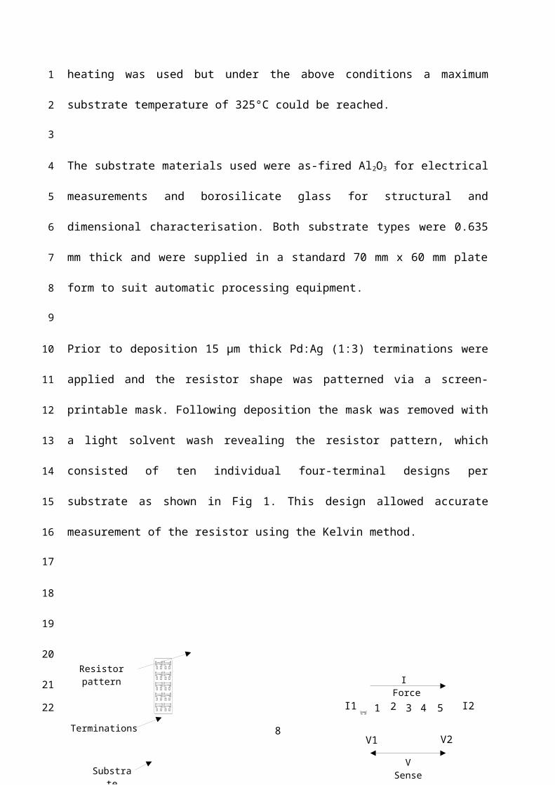
Prior to deposition 15 µm thick Pd:Ag (1:3) terminations were applied and the
resistor shape was patterned via a screen-printable mask. Following deposition the
mask was removed with a light solvent wash revealing the resistor pattern, which
consisted of ten individual four-terminal designs per substrate as shown in Fig 1.
This design allowed accurate measurement of the resistor using the Kelvin method.
Fig 1 - Resistor test substrate pattern (60 x 70 mm).
Samples from each trial were then stabilised for 5 hours at 100, 200, 300, 400 and
500oC in air atmosphere using a Hedinair HT3 oven. The accuracy across the
temperature range 150 to 550ºC was found to be 5ºC.
Electrical resistance measurements were performed at 20°C and 70°C using an
Agilent 3458A digital multimeter and a thermostatically controlled hot plate. TCR was
then calculated using the following equation:
TCR= 1RTref
ΔRΔT
×106 ppm /°C (1)
6
1
2
3
4
5
6
7
8
9
10
11
12
13
14
15
16
17
18
19
20
21
22
23
24
25
26
27

Where RTref is the measured resistance value at 20°C and ∆R is the change in
measured resistance with change in temperature ∆T from 20° to 70°C. Resistance
stability of the films was measured after being subjected to 168 hours at 155°C in air.
Structural images and chemical composition of the film samples sputtered on to
borosilicate glass slides were analysed using an FEI Quanta 200, Scanning Electron
Microscope (SEM) coupled with Energy Dispersive X-ray analysis (EDX). Depth
profiles of the elements were acquired by secondary ion mass spectroscopy (SIMS)
using a 6 keV gallium source as the primary ion beam (MiniSIMS Millbrook
Instruments Ltd) rastered over an area of 100 x 100 m2. In order to eliminate any
artefact from the crater sidewalls a gated area of 10% was used. Film thickness was
measured using a Taylor-Hobson Talystep and optical micrographs of film colour
were taken using a Nikon Measurescope MM-22.
All XRD patterns were collected using a Siemens D5000 diffractometer with Cu Kα
radiation at 40 kV and 40 mA, with a scanning speed of 0.01°/s.
7
1
2
3
4
5
6
7
8
9
10
11
12
13
14
15
16
17
18
19
20
21
22
23
24
25
26
3. Results and Discussion
The electrical properties of the as-grown CuAlMo films with variation in sputtering
pressure are shown in Fig 2. All results are based on the measurement of 20 film
samples. The as-grown thickness of the films was measured to be in the range 900
to 1100 nm.
Fig. 2 – As-grown electrical properties of CuAlMo films with increasing sputtering pressures
In the higher pressure range of 3 to 6 mTorr an increase in sputtering pressure
causes an increase in sheet resistance (Rs) coupled with a decrease in TCR, while
both of these properties are constant in the lower pressure of 1 to 3 mTorr. This
phenomenon could be related to a plateau in deposition rate as the sputtering
pressure approaches the minimum region in which a plasma can be sustained [18-
19]. This pressure range of 1 to 3 mTorr therefore forms a stable region for process
optimisation as variability in electrical properties will be significantly reduced. The
resistance stability (∆Ω/Ω) of films also increases with increasing sputtering
pressure. Films produced in the 1 to 3 mTorr range are the most consistently stable
8
0 1 2 3 4 5 6 70
0.20.40.60.8
11.21.41.61.8
-300
-250
-200
-150
-100
-50
0Rs
Sputtering Pressure (mTorr)
Rs
(Ω/
) & ∆
Ω/Ω
(%)
TCR
(ppm
/ oC
)
1
2
3
4
5
6
7
8
9
10
11
12
13
14
151617
18
19
20
21
22
23
24
25
26

with mean resistance shifts of ~0.5%, whilst those sputtered at higher pressures of 4-
6 mTorr are considerably more unstable with changes of between 0.8 and 1.7%.
This result could be related to the formation of a more porous structure with reduced
grain size and higher defect concentration at higher pressures as suggested by
Thornton’s Model [17] and previously reported for the CuAlMo system [7]. However,
even the result of ~0.5% reported for the lower pressure range of 1 to 3 mTorr is
outside the target specification of 0.25% and suggests that post deposition annealing
is required in order to improve the stability of the thin films.
The combined effects of sputtering pressure and heat treatment temperature on the
sheet resistance, TCR and resistance stability of the films are shown in Fig 3.
9
Fig. 3 – Effect of sputtering pressure and heat treatment temperatureon the electrical properties of the
CuAlMo films.
grownas
(a) – Sheet Resistance
grownas
(b) – TCR
grownas
(c) – Resistance Stability
1
2
3
4
5
6
7
8
9
10
11
12
13
14
15
16
17
18
19
20
21
22
23
24
25

The reduction in sheet resistance (Rs) with increasing heat treatment temperature
follows a similar curvature for films grown at different sputtering pressures (Fig 3a).
The results for films sputtered at 1 to 3 mTorr are consistent in the range 0.1 to 0.2
Ω/, whilst those sputtered at higher pressures have increased sheet resistances
with a maximum value of ~0.6 Ω/at 6 mTorr.
The results for TCR follow an inverse trend to the sheet resistance plots, their values
being shifted towards higher values with increasing heat treatment temperature (Fig
3b). Again results obtained for the films grown in the pressure range of 1 to 3 mTorr
are comparable and all pass through the zero TCR line at 400 to 430 ºC. For films
grown in the higher pressure range of 4 to 6 mTorr, the as-grown TCR becomes
increasingly negative and for those sputtered at 5 and 6 mTorr, a zero TCR is not
attainable at the maximum annealing temperature of 500 ºC.
Films grown in the 1 to 3 mTorr range are also the most stable (Fig 3c). The plot of
stability versus annealing temperature follows a similar trend for all films, the
greatest reduction being made for films treated at 200 ºC, which is above the dry
heat stability test temperature of 155 ºC. This stability improvement with increasing
heat treatment temperature continues up to 300 ºC at which point the films are at
their most stable. Beyond this temperature the resistance stability of the films begins
to decline with the level of deterioration appearing to be a function of initial sputtering
pressure. For the films grown in the 1 to 3 mTorr range and subsequently annealed
at temperatures of 300 and 500 ºC this increase is less than 0.10 %, compared to
0.25 to 0.70 % for films sputtered at higher pressures of 4 to 6 mTorr.
10
1
2
3
4
5
6
7
8
9
10
11
12
13
14
15
16
17
18
19
20
21
22
23
24
25

The reason for this decrease in resistance stability of films grown at higher sputtering
pressures, especially when treated at higher annealing temperatures, could be
related to the more open porous structure which lends itself to higher levels of
impurity incorporation during deposition and also makes it more susceptible to attack
in high temperature oxidising environments.
To investigate this theory further the level of oxygen present in the films before and
after heat treatment was measured using SEM-EDX. The chemical composition for
films sputtered on glass at pressures of 1, 3 and 5 mTorr and subsequently annealed
at 300 and 450 ºC are presented in Fig 4. All results are based on an average of 3
measurements at different areas of the film surface. The films were found to be
homogeneous with variation in results of less than 2 at.%.
11
(a) - 1 mTorr
Fig. 4 – Mean chemical composition with increasing heat treatment temperature for CuAlMo films
grown on glass at 1, 3 and 5 mTorr.
(b) - 3 mTorr
(c) - 5 mTorr
1
2
3
4
5
6
7
8
9
10
11
12
13
14
15
16
17
18
19
20
21
22
23
24

For the films deposited at 1 mTorr (Fig 4a) and 3 mTorr (Fig 4b) the as-grown
compositions are almost identical with the concentration of oxygen being <3 at.%.
There is also a small level of Si present in the films which originates from the
borosilicate substrate beneath. Following heat treatment at 300 ºC for 5 hours, the
oxygen levels increases to ~6 at.% and after treatment at 450 ºC there are further
increases to ~7 at.% suggesting the formation of aluminium and copper oxides.
There is no noticeable change in the level of Si with increasing heat treatment
temperature.
For the films deposited at 5 mTorr (Fig 4c) there is an increase in the oxygen content
to 4.5 at.%, whilst that of the Si remains at <1 at.%. This increase is further
augmented during heat treatment, and following annealing for 5 hours at 300 ºC the
level of oxygen in the film has increased rapidly to above 11 at.%.
This result suggests that higher levels of aluminium oxide and copper oxide are
formed in the films sputtered at higher pressures. The reaction is even further
accelerated at an annealing temperature of 450 ºC, where the oxygen content has
increased to over 22 at.%. This result could be attributed to the more open porous
structure of the film which makes it susceptible to attack from the oxygen containing
environment, a reaction which is known to increase rapidly with temperature. There
is also an uncharacteristic increase in the Si content of the films with temperature.
Again this result is thought to relate to the porous structure allowing access to the
underlying glass substrate.
12
1
234
5
6
7
8
9
10
11
12
13
14
15
16
17
18
19
20
21
22
23
24
25
26

The above chemical analysis results correlate well with the stability measurements
reported in Fig 3c and are further supported by visual analysis of the film surface
before and after heat treatment. Fig 5 shows optical micrographs of CuAlMo films
grown at pressures of 3 and 5 mTorr in both the freshly deposited and annealed
state.
Fig. 5 – Photos of CuAlMo films on Al2O3 showing changes in film colour with sputtering pressure and heat treatment
For the as-grown samples there is very little difference in the visual appearance of
the films deposited at different pressures and both are silver in colour. Following
annealing at 450 ºC for 5 hours there are noticeable changes for both films. There is
a slight darkening in colour of the film grown at 3 mTorr. However the film grown at 5
mTorr has changed in colour to a golden brown, again suggesting the formation of
copper oxide.
13
5 mTorr - H.T. at 450 ºC for 5 hours5 mTorr – as-grown
3 mTorr - H.T. at 450 ºC for 5 hours3 mTorr - as-grown
2.5mm
1
2
3
4
5
6
7
8
9
10
1112
13
14
15
1617181920
21
22
23
24
25
26
27

To confirm that the formation of an aluminium oxide layer was responsible for the
superior stability properties of the films grown at lower pressures, depth profiles of
the elements were performed by SIMS. Fig 6 shows the results for a CuAlMo film
grown at 3 mTorr and annealed at 450 ºC for 5 hours in air.
Fig. 6 – SIMS analysis of a CuAlMo film grown on Al2O3 at 3 mTorr and heat treated in air for 5 hours at 450ºC.(thin line = as-grown, thick line = annealed)
For the freshly deposited film the concentrations of Mo and Cu and Al are uniform
with depth. Although it is noted that Cu and Al depth profiles present a slight
increasing gradient for the first 500 nm. This could be due to some oxygen
incorporation during the deposition as the substrate temperature gets higher towards
the end of the deposition. After heat treatment a gradient in the Mo signal near the
film/substrate interface is observed. The Al signal retains its shape following
annealing but the intensity is slightly increased again due to the increased presence
of oxygen in the film as explained next. The oxygen signal intensity in the film is
doubled following annealing and the formation of an aluminium oxide layer at the
surface is observed for the first 50 nm. The formation of this superficial layer is also
indicated by the delay before the start of the Cu signal. It is expected that some level
14
(b) – positive ions (a) – negative ions
1
2
3
4
5
6
7
8
9
10
11
12
1314151617
18
19
20
21
22
23
24
25
26
27
28

of oxidation to be present throughout the film thickness. Cu shows the most variation
with a strong gradient in the first part of the CuAlMo film. This gradient is possibly
due to (i) Cu diffusion during the annealing process or (ii) enhancement of the Cu
signal due to the high oxygen content from the aluminium oxide layer.
Fig 6 shows SEM micrographs of surface morphology for films sputtered on glass at
pressures of 1mTorr and 5mTorr. There appears to be very little difference between
the morphology of the films grown at different pressures. For both films the structure
is very fine grained and is typical of an amorphous material. The production of fined
grained materials is frequently encountered when sputtering multi component
materials due to the reduction in grain boundary mobility [20-21] and is regularly
reported for thin resistive films such as NiCr [22-25].
(a) 1mTorr (b) 5mTorr
Fig. 6 – SEM micrographs of CuAlMo films grown on glass substrates (Magnification x240K)
15
100nm100nm 100nm100nm100nm100nm100nm100nm100nm100nm100nm100nm100nm100nm100nm100nm100nm100nm100nm100nm100nm100nm100nm100nm100nm100nm100nm100nm100nm100nm100nm100nm100nm100nm
1
2
3
4
5
6
7
8
9
10
11
12
13
14
15
16
17
1819202122
23
24
25
26
27
28

Fig 8 shows XRD results for films sputtered at 1000 W and 3 mTorr and annealed in
air at various temperatures for 5 hours.
Fig. 8 – XRD patterns arount the (330) reflection for CuAlMo films grown at 1000 W and 3 mTorr and heat treated for 5 hours in air at various temperatures.
Only one reflection belonging to a metallic phase was detected in the XRD pattern
and this was identified as the (330) plane of the 2 (Cu9Al4) phase. The 2 phase is
known to be stable for an Al composition range of 31 to 37 at.% for bulk samples [26]
and has been shown to be stable over a much wider compositional range (28 to 62
at.% Al) for thin films [27]. This composition corresponds well with the current work
where the Al content was measured to be 36 to 38 at.%. Furthermore the
temperatures involved in the phase formation are also consistent with those
characterised by the CuAl phase diagram [28]. The XRD analysis indicated no
incorporation of Mo into the 2 phase. It is likely that the low temperature processes
used here do not allow miscibility between the three elements.
There is a clear increase in the crystallinity of the films with annealing temperature
as indicated by the reduction in the peak width and its higher intensity. The relatively
small difference in intensity between the as-grown film and the film annealed at 300
16
41 42 43 44 45 46 470
100
200
3005hrs, 500ºC5hrs, 400ºC5hrs, 300ºCas grown
2θ (degree)
Inte
nsity
(x10
00)
1
2
3
4
56789
101112131415161718192021
22
23
24
25
26
27
28
29
30
31
32
33
34
35

ºC can be related to the similarity in substrate temperature during deposition, which
was reported to be 325 ºC for a cathode power of 1000 W [7].
Using the XRD results, the average (330) crystallite size of the films can be related
to the variation in the full width half maximum (FWHM) for the (330) peak and is
calculated using the Scherrer equation [29]:
L= KλFWHM cosθ (2)
Where L is the crystallite size, K is the Scherrer constant (=0.90), is the wavelength
of the x-ray and is the Bragg angle.
The variation in FWHM and mean crystallite size, calculated using the Scherrer
equation, as a function of annealing temperature are plotted in Fig 9.
Fig. 9 – Variation in FWHM and corresponding calculated mean crystallite size for CuAlMo films grown at 1000 W and 3 mTorr and heat treated for
5 hours in air at various temperatures.
The average crystallite size increases from 14 to 24 nm with increasing heat
treatment temperature. The results correspond well with change in the electrical
17
as grown
300 400 5000
0.2
0.4
0.6
0.8
1
0
5
10
15
20
25
30
FWHMCrystallite Size
Heat Treatment Temperature (oC)
FWH
M (d
egre
e)
Cry
stal
lite
Siz
e (n
m)
1
2
3
4
5
6
7
89
10
11
12
13
14
15
16
17
18
19
20
21
22
2324252627
28
29

properties of the films reported in Fig 3. The increase in crystallite size is also likely
to yield an overall increase in grain size and consequently a decrease in grain
boundaries, leading to an increase in the conductivity of the films due to the
reduction in charge-carrier scattering by grain boundaries [22].
The electrical properties of films grown at 1 and 3 mTorr as a function of annealing
time at 425 ºC, the approximate temperature required to achieve zero TCR, are
presented in Fig 10.
It appears that a minimum heat treatment time of 3 to 4 hours is required to give
stable electrical properties. For films sputtered at both 1 and 3 mTorr it takes 3 hours
18
(c) – Resistance Stability
Fig. 10 – Effect of heat treatment duration at 425ºC on the electrical
properties of CuAlMo films grown at sputtering pressures of 1 and 3 mTorr.
(b) - Sheet Resistance (a) - TCR
1
2
3
4
5
6
7
8
9
10
11
12
13
14
15
16
17
18
19
20
21
22
23
24
25

at 425 ºC for the TCR to increase from an as-grown value of -90 to a final value of 0
± 10 ppm/ºC (Fig 10b). Further heat treatment time has negligible effect on TCR and
it remains better than 0 ± 20 ppm/ºC across the range 3 to 7 hours.
The films are also at their most stable in this time range and typical resistance shifts
of less than 0.2 % following storage in air for 168 hours at 155 ºC are achieved for
films sputtered at both 1 and 3 mTorr (Fig 10c).
19
1
2
3
4
5
6
7
8
9
10
11
12
13
14
15
16
17
18
19
20
21
22
23
24
25

4. Conclusions
This work has shown that the electrical properties of the CuAlMo thin films are not
only a function of their chemical composition but also strongly depend on the
sputtering and heat treatment process settings. To obtain films of low sheet
resistance with near zero TCR and good long term stability, a low sputtering
pressure in the range 1 to 3 mTorr is required.
The development of the CuAlMo film structure during sputtering follows the classical
Thornton’s model [17]. For films sputtered at high power (1000 W) and low pressure
(1-3 mTorr), a more dense structure with lower impurity level is produced.
Conversely for films grown at higher pressures (4-6 mTorr) the resulting structure is
more porous with a higher content of impurities being incorporated during deposition.
Subsequent annealing of the films in air results in re-crystallisation which gives a
decrease in sheet resistance coupled with an increase in TCR. The mean crystallite
size in the film was 14 nm when deposited at 1000 W and 3 mTorr and grew to 24
nm following annealing at 500ºC for 5 hours in air. For films grown at pressures of 1
to 3 mTorr the TCR can be controlled around the zero line following heat treatment
at 425 ºC for a minimum of 3 hours. For films grown at higher sputtering pressures
the TCR is much more negative and cannot be heat treated to zero whilst
maintaining acceptable resistance stability.
From this work a set of optimum sputtering and heat treatment process parameters
have been concluded. These settings have been used to manufacture production
size batches of CuAlMo thin film chip resistors for long term reliability testing.
20
1
2
3
4
5
6
7
8
9
10
11
12
13
14
15
16
17
18
19
20
21
22
23
24
25

Acknowledgements
This work was funded and supported by TT Electronics, Welwyn Components Ltd
and an Industrial Fellowship awarded by The Royal Commission for the Exhibition of
1851.
References
[1] E. Bloch, D. Mistele, R. Brener, C. Cytermann, A. Gavrilov, D. Ritter, Semicond. Sci. Technol. 26 (2011) 105004.
[2] R. Driad, M. Krieg, N. Geldmacher, J. Ruster, F. Benkhelifa, J. Electrochem. Soc. 158 (2011) H561.
[3] BJ. Lee, S. Lee, PK. Shin, Jpn. J. Appl. Phys. 48 (2009) 055502.
[4] J. Van Den Broek, R. Van Der Rijt, J. Janssen, Philips. J. Res. 51 (1998) 429.
[5] B. Kang, S. Hur, D. Kim, S. Yoon, Electrochem. Solid. St. 8 (2005) G92.
[6] M. Birkett, J. Brooker, R. Penlington, A. Wilson, K. Tan, IET. Sci. Meas. Technol. 2 (2008) 304.
[7] M. Birkett, Birmingham, UK., September 11 13, 2012, Proceedings of the 26 th International Conference on Manufacturing Research, ICMR, (2012) 504.
[8] S. Chandra, S. Uthanna, G. Rao, Appl. Surf. Sci. 254 (2008) 1953.
[9] A. Das, C. Grabbe, R. Hufnagel. Newport Beach, USA, March 17 20, 2008, Proceedings of the 28th Capacitor and Resistor Technology Symposium, CARTS, (2008) 339.
[10] S. Lee, S. Wang, J. Chen, J. Huang, Thin Solid Films 515 (2006) 1069.
[11] Martin, F., P. Muralt, M. Dubois, J. Vac. Sci. Technol. A. 24 (2006) 946.
[12] M. Sinha, S. Mukherjee, B. Pathak, R. Paul, P. Barhai, Thin Solid Films 515 (2006) 1753.
[13] G. Zhigal’skii, B. Jones, Electrocomponent Science Monographs – The Physical Properties of Thin Metal Films, Taylor and Francis Publications, London, 2003, P. 1.
[14] L. Maissel, R. Glang, (1970), Handbook of Thin Film Technology, McGraw-Hill Publications, New York, 1970, p. 18-4.
[15] R. Thun, in: G. Hass (Ed.) Physics of thin films, Advances in Research and Development, vol. 1, Gordon and Breach Publications, New York, 1963, p. 187.
21
1
2
3
4
5
67
89
10
11
12
1314
1516
17181920212223242526272829303132333435363738

[16] K. Chopra, (1969), Thin Film Phenomena, McGraw-Hill Publications, New York, 1969, p. 23.
[17] J. Thorton, Annu. Rev. Mater. Sci. 7 (1977) 239.
[18] H. Khatri, J. Phy-Conden. Mat. 20 (2008) 5055206.
[19] K. Chan and B. Teo, J. Mater. Sci. 40 (2005) 5971.
[20] C. Thompson and R. Carel, J. Mech. Phys. Solids. 44 (1996) 657.
[21] C. Thompson, Interface Sci. 6 (1998) 85.
[22] Y. Kwon, N. Kim, G. Choi, W. Lee, Y. Seo, J. Park, Microelectron Eng. 82 (2005) 314.
[23] S. Vinayak, H. Vyas, K. Muraleedharan V. Vankar, Thin Solid Films. 514 (2006) 52.
[24] N. Phuong, D. Kim, B. Kang, C. Kim, S. Yoon, J. Electrochem. Soc. 153 (2006) G27.
[25] M. Nguyen and S. Yoon, J. Electrochem. Soc. 153 (2006) G606.
[26] C. Macchioni, J. Rayne, C. Bauer, Phys. Rev. B. 25 (1982) 3865.
[27] V. Bashev, F. Dotsenko, I. Miroshnichenko, Fiz. Met. Metalloved. 70 (1990) 203.
[28] ASM Handbooks, Alloy Phase Diagrams, ASM International, Materials Park, Ohio, 3 (2002) 234.
[29] B. Cullity, Elements of x-ray diffraction, Addison-Wesley Publishing Company,Boston, 1978, p. 102.
22
123456789
101112131415161718192021222324252627282930313233


![Computing Science: Mobile App Development - … · Web viewComputing Science Mobile App Development Advice for Practitioners [NATIONAL 4] This advice and guidance has been produced](https://img.pdfslide.us/doc/110x75/5b1b57fb7f8b9a19258e9758/computing-science-mobile-app-development-web-viewcomputing-science-mobile.jpg)