Embed Size (px)
Citation preview
October 22, 2006October 22, 2006 11
Novel RollNovel Roll--toto--Roll Manufacturing Techniques Roll Manufacturing Techniques for Patterning Conductive Layersfor Patterning Conductive Layers
Fall 2006 AIMCAL Technical ConferenceFall 2006 AIMCAL Technical Conference
57 Smith Place57 Smith Place
Cambridge, MA 02138Cambridge, MA 02138
www.microcontinuum.comwww.microcontinuum.com
W. Dennis Slafer / Robert PrainoW. Dennis Slafer / Robert Praino
617.354.1092617.354.1092
October 22, 2006October 22, 2006
22MicroContinuum, IncCambridge, MA
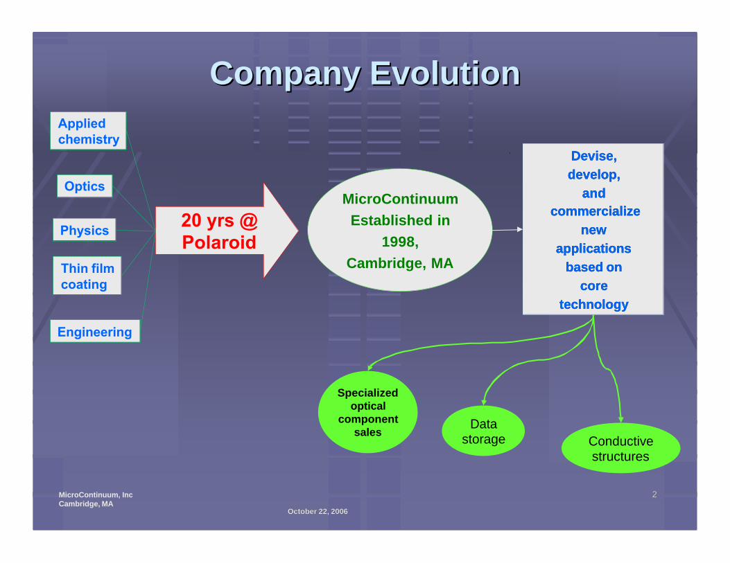
Company EvolutionCompany Evolution
Devise, Devise,
develop,develop,
andand
commercialize commercialize
new new
applications applications
based on based on
core core
technologytechnology
20 yrs @ Polaroid
MicroContinuum
Established in
1998,
Cambridge, MA
Physics
Applied chemistry
Engineering
Optics
Thin film coating
Specialized optical
component sales
Data storage Conductive
structures
October 22, 2006October 22, 2006
33MicroContinuum, IncCambridge, MA
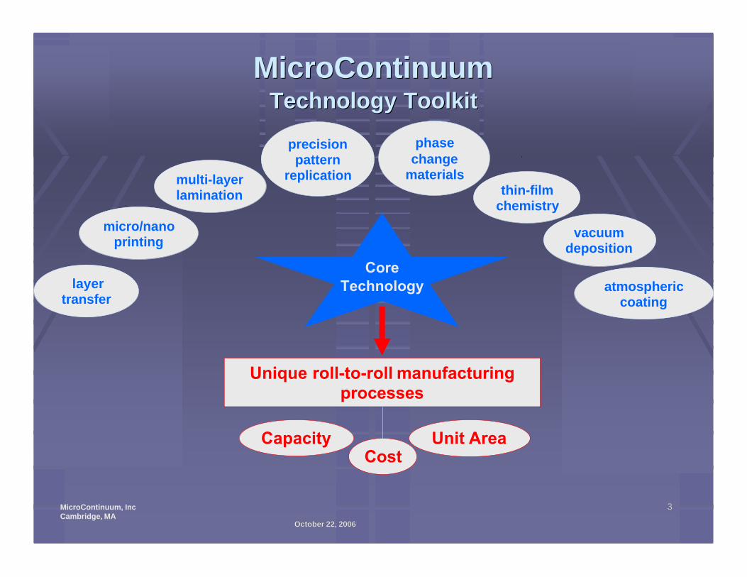
MicroContinuumMicroContinuumTechnology ToolkitTechnology Toolkit
Unique roll-to-roll manufacturing processes
vacuum deposition
layer transfer
multi-layer lamination thin-film
chemistry
precision pattern
replication
micro/nanoprinting
phase change
materials
Core Technology
CostCapacity Unit Area
atmospheric coating
October 22, 2006October 22, 2006
44MicroContinuum, IncCambridge, MA
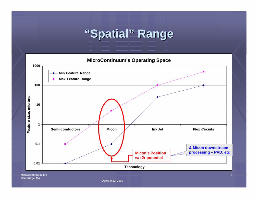
MicroContinuum's Operating Space
0.01
0.1
1
10
100
1000
Semi-conductors Micon Ink Jet Flex Circuits
Technology
Fe
atu
re s
ize
, m
icro
ns
Min Feature Range
Max Feature Range
““SpatialSpatial”” RangeRange
Micon’s Positionw/ r2r potential
& Micon downstream processing – PVD, etc
October 22, 2006October 22, 2006
55MicroContinuum, IncCambridge, MA
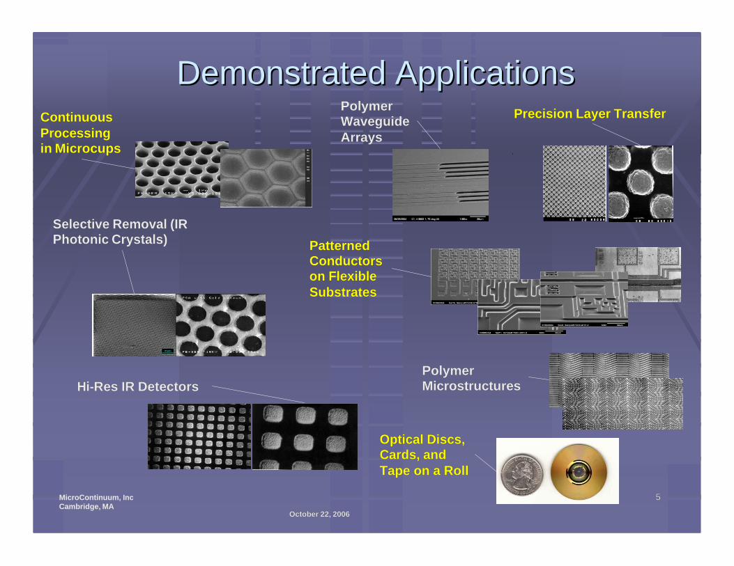
Demonstrated ApplicationsDemonstrated Applications
Optical Discs, Optical Discs, Cards, and Cards, and Tape on a RollTape on a Roll
Precision Layer TransferPrecision Layer TransferContinuous Continuous Processing Processing in Microcupsin Microcups
Patterned Patterned Conductors Conductors on Flexible on Flexible Substrates Substrates
Selective Removal (IR Selective Removal (IR Photonic Crystals)Photonic Crystals)
HiHi--Res IR DetectorsRes IR DetectorsPolymer Polymer MicrostructuresMicrostructures
Polymer Polymer Waveguide Waveguide ArraysArrays
October 22, 2006October 22, 2006
66MicroContinuum, IncCambridge, MA
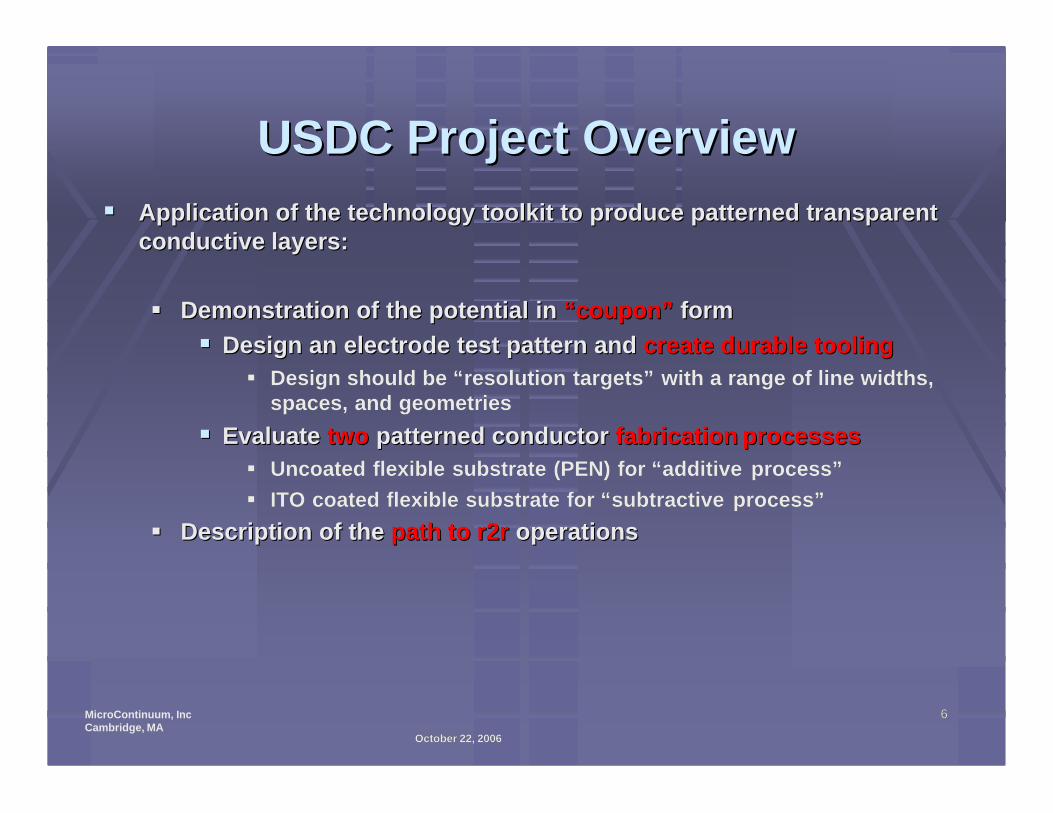
USDC Project Overview USDC Project Overview
§§ Application of the technology toolkit to produce patterned transApplication of the technology toolkit to produce patterned transparent parent conductive layers: conductive layers:
§§ Demonstration of the potential in Demonstration of the potential in ““couponcoupon”” formform
§§ Design an electrode test pattern and Design an electrode test pattern and create durable toolingcreate durable tooling
§§ Design should be Design should be ““resolution targetsresolution targets”” with a range of line widths, with a range of line widths, spaces, and geometriesspaces, and geometries
§§ Evaluate Evaluate twotwo patterned conductor patterned conductor fabrication processesfabrication processes
§§ Uncoated flexible substrate (PEN) for Uncoated flexible substrate (PEN) for ““additive processadditive process””
§§ ITO coated flexible substrate for ITO coated flexible substrate for ““subtractive processsubtractive process””
§§ Description of the Description of the path to r2rpath to r2r operations operations
October 22, 2006October 22, 2006
77MicroContinuum, IncCambridge, MA
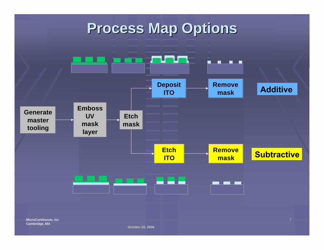
Process Map OptionsProcess Map Options
Additive
Generate master tooling
Emboss UV
mask layer
Etch mask
Deposit ITO
Remove mask
Etch ITO
Remove mask Subtractive
October 22, 2006October 22, 2006
88MicroContinuum, IncCambridge, MA
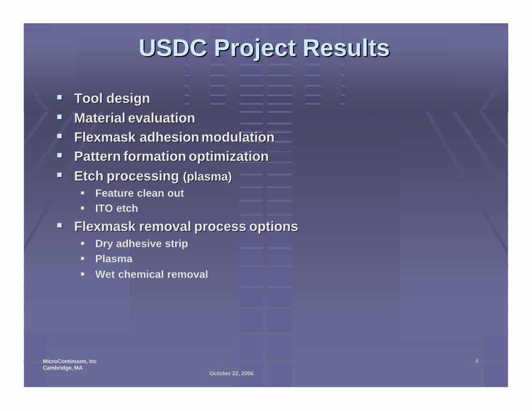
USDC Project Results USDC Project Results
§§ Tool designTool design
§§ Material evaluation Material evaluation
§§ FlexmaskFlexmask adhesion modulationadhesion modulation
§§ Pattern formation optimization Pattern formation optimization
§§ Etch processing Etch processing (plasma) (plasma)
§§ Feature clean out Feature clean out
§§ ITO etch ITO etch
§§ FlexmaskFlexmask removal process optionsremoval process options§§ Dry adhesive strip Dry adhesive strip
§§ Plasma Plasma
§§ Wet chemical removal Wet chemical removal
October 22, 2006October 22, 2006
99MicroContinuum, IncCambridge, MA
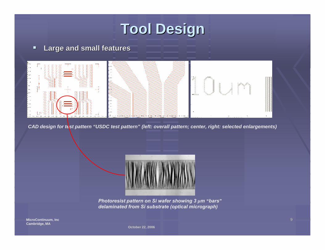
Tool DesignTool Design§§ Large and small featuresLarge and small features
Photoresist pattern on Si wafer showing 3 µm “bars”delaminated from Si substrate (optical micrograph)
CAD design for test pattern “USDC test pattern” (left: overall pattern; center, right: selected enlargements)
October 22, 2006October 22, 2006
1010MicroContinuum, IncCambridge, MA
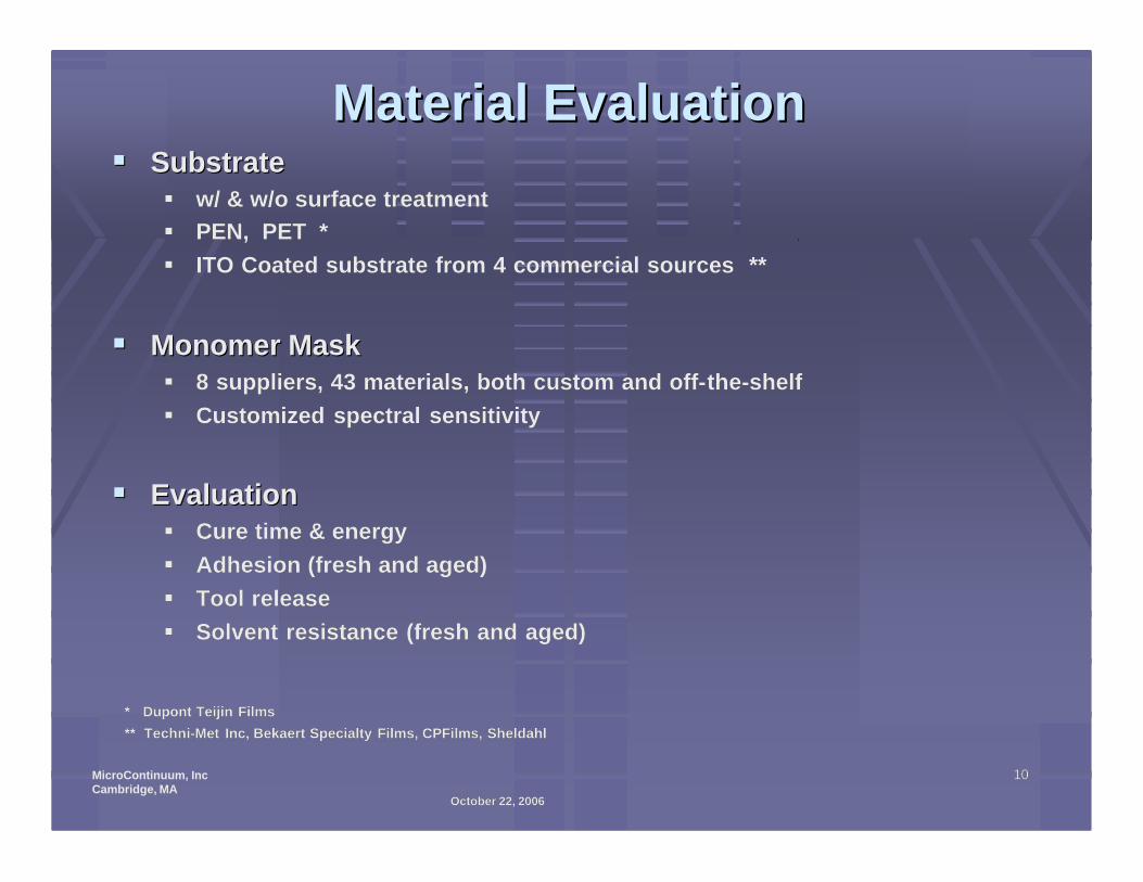
Material EvaluationMaterial Evaluation§§ SubstrateSubstrate
§§ w/ & w/o surface treatmentw/ & w/o surface treatment
§§ PEN, PET *PEN, PET *
§§ ITO Coated substrate from 4 commercial sources **ITO Coated substrate from 4 commercial sources **
§§ Monomer MaskMonomer Mask§§ 8 suppliers, 43 materials, both custom and off8 suppliers, 43 materials, both custom and off--thethe--shelf shelf
§§ Customized spectral sensitivity Customized spectral sensitivity
§§ EvaluationEvaluation§§ Cure time & energyCure time & energy
§§ Adhesion (fresh and aged) Adhesion (fresh and aged)
§§ Tool release Tool release
§§ Solvent resistance (fresh and aged) Solvent resistance (fresh and aged)
* * DupontDupont Teijin FilmsTeijin Films
** ** TechniTechni--Met Inc, Met Inc, BekaertBekaert Specialty Films, Specialty Films, CPFilmsCPFilms, , SheldahlSheldahl
October 22, 2006October 22, 2006
1111MicroContinuum, IncCambridge, MA
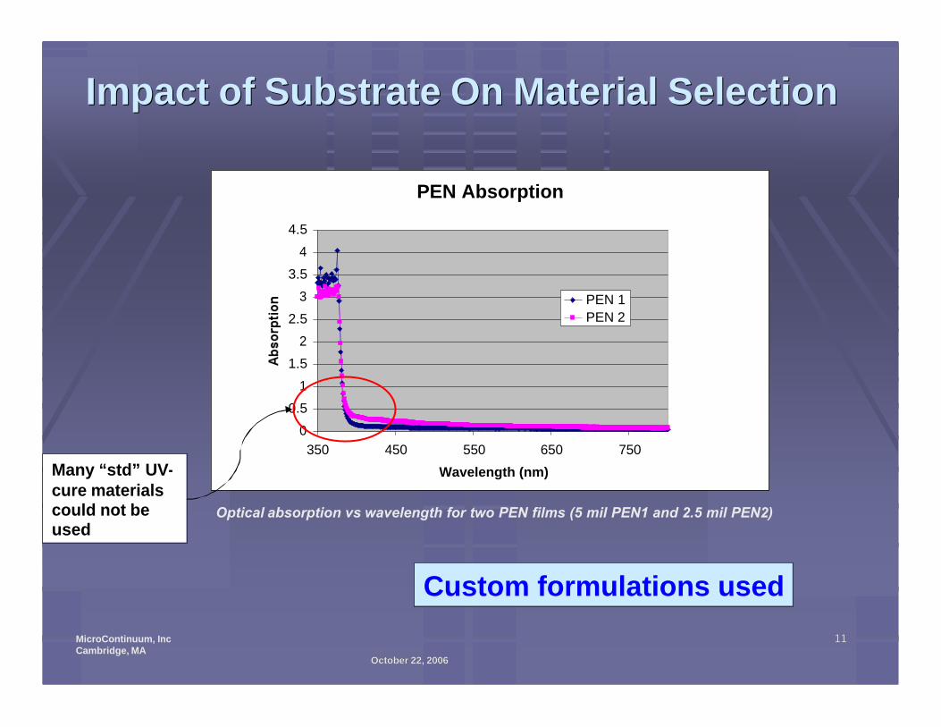
Impact of Substrate On Material SelectionImpact of Substrate On Material Selection
PEN Absorption
0
0.5
1
1.5
2
2.5
3
3.5
4
4.5
350 450 550 650 750
Wavelength (nm)
PEN 1
PEN 2
Optical absorption vs wavelength for two PEN films (5 mil PEN1 and 2.5 mil PEN2)
Many “std” UV-cure materials could not be used
Custom formulations used
October 22, 2006October 22, 2006
1212MicroContinuum, IncCambridge, MA
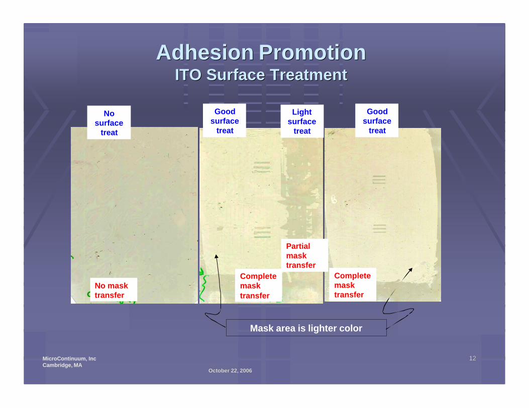
Adhesion Promotion Adhesion Promotion ITO Surface TreatmentITO Surface Treatment
Complete mask transfer
No mask transfer
Partial mask transfer
Complete mask transfer
No surface
treat
Light surface
treat
Good surface
treat
Good surface
treat
Mask area is lighter color
October 22, 2006October 22, 2006
1313MicroContinuum, IncCambridge, MA
Pattern FormationPattern Formation
October 22, 2006October 22, 2006
1414MicroContinuum, IncCambridge, MA
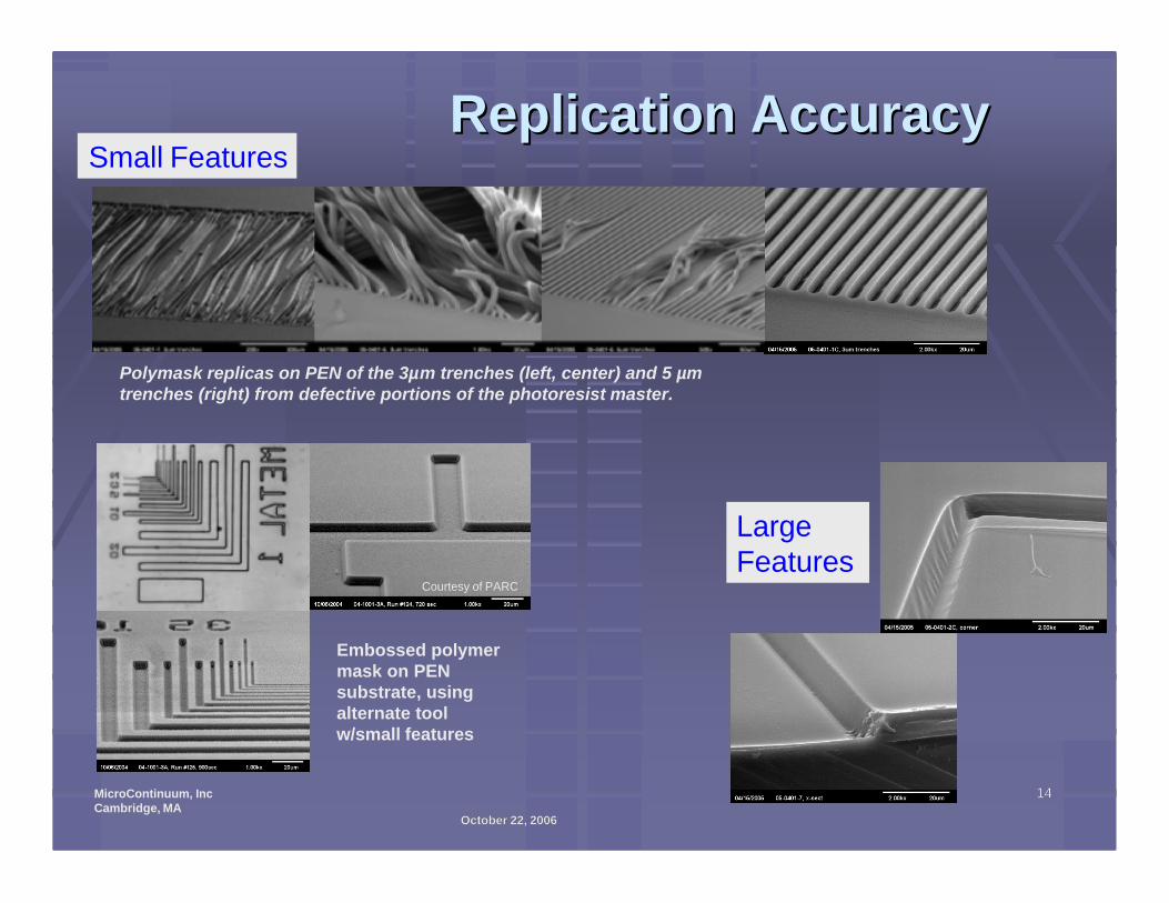
Replication Accuracy Replication Accuracy
Polymask replicas on PEN of the 3µm trenches (left, center) and 5 µm trenches (right) from defective portions of the photoresist master.
Small Features
Large Features
Embossed polymer mask on PEN substrate, using alternate tool w/small features
Courtesy of PARC
October 22, 2006October 22, 2006
1515MicroContinuum, IncCambridge, MA
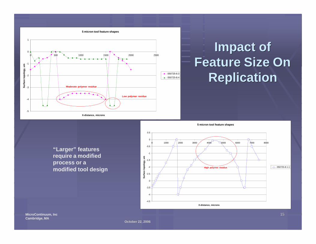
Impact of Impact of Feature Size On Feature Size On
ReplicationReplication
5 micron tool feature shapes
-5
-4
-3
-2
-1
0
1
0 500 1000 1500 2000 2500
X-distance, microns
Su
rface t
op
olo
gy, u
m
050725-8.3
050725-8.4
Moderate polymer residue
Low polymer residue
5 micron tool feature shapes
-4.5
-4
-3.5
-3
-2.5
-2
-1.5
-1
-0.5
0
0.5
0 1000 2000 3000 4000 5000 6000 7000 8000
X-distance, microns
Su
rface t
op
olo
gy, u
m
050725-8.1.1High polymer residue
“Larger” features require a modified process or a modified tool design
October 22, 2006October 22, 2006
1616MicroContinuum, IncCambridge, MA
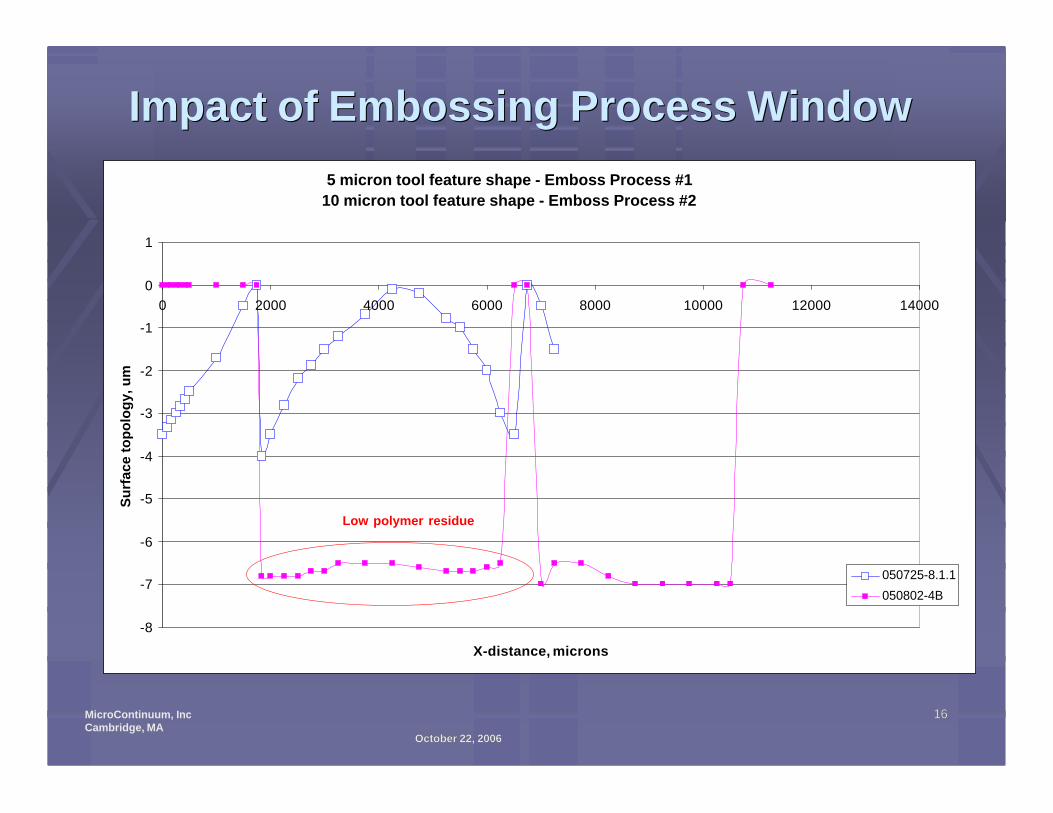
Impact of Embossing Process WindowImpact of Embossing Process Window
5 micron tool feature shape - Emboss Process #1
10 micron tool feature shape - Emboss Process #2
-8
-7
-6
-5
-4
-3
-2
-1
0
1
0 2000 4000 6000 8000 10000 12000 14000
X-distance, microns
Su
rface t
op
olo
gy, u
m
050725-8.1.1
050802-4B
Low polymer residue
October 22, 2006October 22, 2006
1717MicroContinuum, IncCambridge, MA
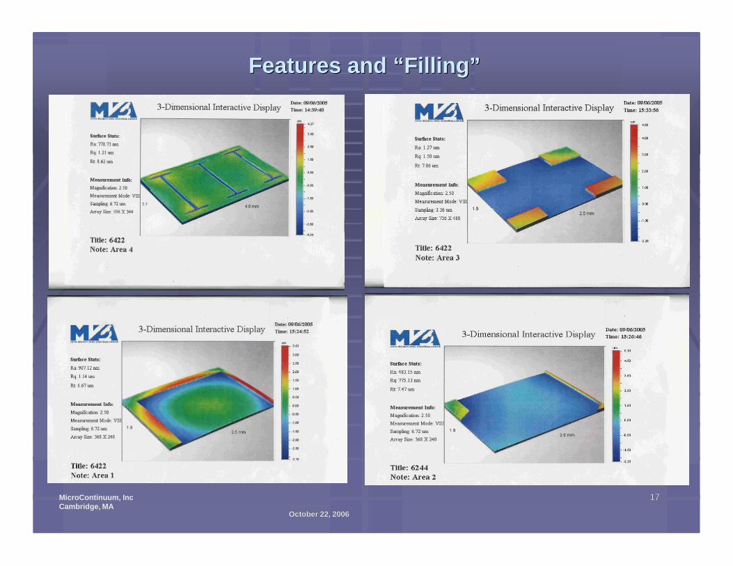
Features and Features and ““FillingFilling””
October 22, 2006October 22, 2006
1818MicroContinuum, IncCambridge, MA
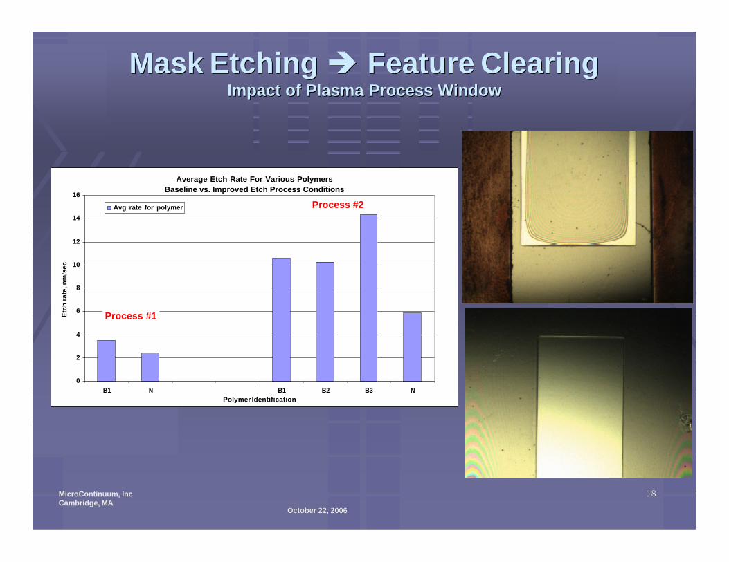
Mask Etching Mask Etching èè Feature Clearing Feature Clearing Impact of Plasma Process WindowImpact of Plasma Process Window
Average Etch Rate For Various Polymers
Baseline vs. Improved Etch Process Conditions
0
2
4
6
8
10
12
14
16
B1 N B1 B2 B3 N
Polymer Identification
Etc
h r
ate
, n
m/s
ec
Avg rate for polymer
Process #1
Process #2
October 22, 2006October 22, 2006
1919MicroContinuum, IncCambridge, MA
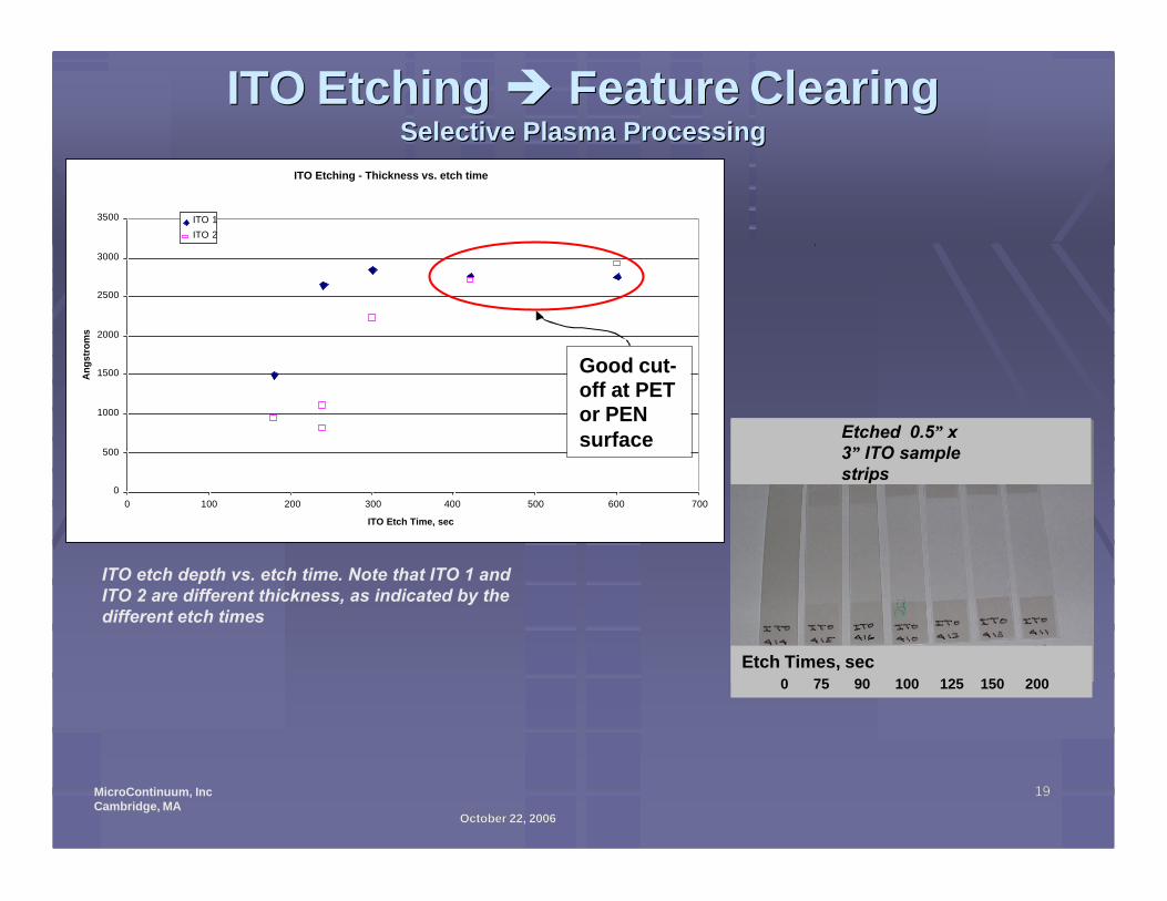
ITO Etching ITO Etching èè Feature Clearing Feature Clearing Selective Plasma ProcessingSelective Plasma Processing
ITO etch depth vs. etch time. Note that ITO 1 and ITO 2 are different thickness, as indicated by the different etch times
ITO Etching - Thickness vs. etch time
0
500
1000
1500
2000
2500
3000
3500
0 100 200 300 400 500 600 700
ITO Etch Time, sec
An
gs
tro
ms
ITO 1
ITO 2
Good cut-off at PET or PEN surface
Etch Times, sec0 75 90 100 125 150 200
Etched 0.5” x 3” ITO sample strips
October 22, 2006October 22, 2006
2020MicroContinuum, IncCambridge, MA
Polymer Mask StripPolymer Mask Strip§§ Dry Dry flexmaskflexmask delaminationdelamination (with adhesive strip sheet) not robust with (with adhesive strip sheet) not robust with
material set tested tomaterial set tested to--date date
§§ Plasma processing impactPlasma processing impact
§§ AgingAging
§§ Plasma Plasma flexmaskflexmask etching etching
§§ Process cycle time is slow Process cycle time is slow (influenced by mask thickness)(influenced by mask thickness)
§§ May be impacted by plasma process equipment used (May be impacted by plasma process equipment used (r/dr/d scale) scale)
§§ Long process time impact on substrate (in Long process time impact on substrate (in ““ITO clearedITO cleared”” areas)areas)
§§ Wet processing Wet processing
§§ Initial results Initial results –– robust removal raterobust removal rate
§§ Offers potential cost benefitOffers potential cost benefit
October 22, 2006October 22, 2006
2121MicroContinuum, IncCambridge, MA
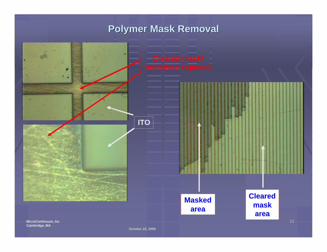
Polymer Mask RemovalPolymer Mask Removal
ITO
Cleared mask/ substrate exposed
Masked area
Cleared mask area
October 22, 2006October 22, 2006
2222MicroContinuum, IncCambridge, MA
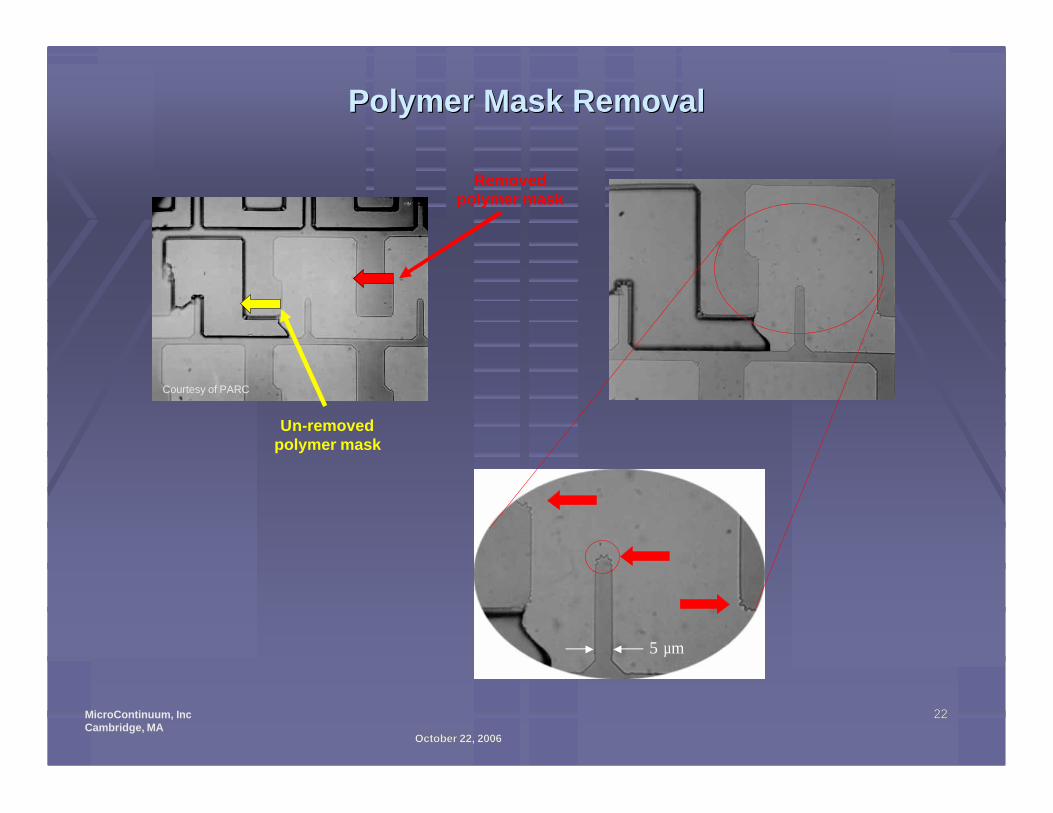
Polymer Mask Removal Polymer Mask Removal
5 µm
Courtesy of PARC
Un-removed polymer mask
Removed polymer mask
October 22, 2006October 22, 2006
2323MicroContinuum, IncCambridge, MA
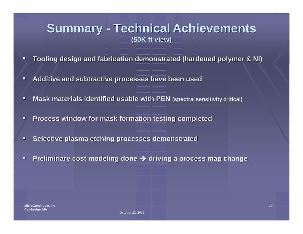
Summary Summary -- Technical Achievements Technical Achievements (50K ft view)(50K ft view)
§§ Tooling design and fabrication demonstrated (hardened polymer & Tooling design and fabrication demonstrated (hardened polymer & Ni)Ni)
§§ Additive and subtractive processes have been usedAdditive and subtractive processes have been used
§§ Mask materials identified usable with PEN Mask materials identified usable with PEN (spectral sensitivity critical) (spectral sensitivity critical)
§§ Process window for mask formation testing completedProcess window for mask formation testing completed
§§ Selective plasma etching processes demonstrated Selective plasma etching processes demonstrated
§§ Preliminary cost modeling done Preliminary cost modeling done èè driving a process map change driving a process map change
October 22, 2006October 22, 2006
2424MicroContinuum, IncCambridge, MA
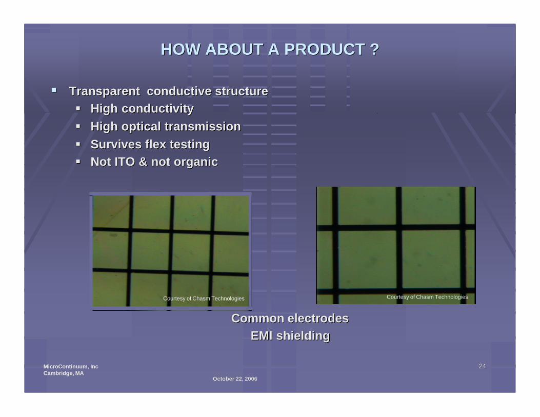
HOW ABOUT A PRODUCT ? HOW ABOUT A PRODUCT ?
§§ Transparent conductive structure Transparent conductive structure
§§ High conductivityHigh conductivity
§§ High optical transmissionHigh optical transmission
§§ Survives flex testing Survives flex testing
§§ Not ITO & not organic Not ITO & not organic
Common electrodesCommon electrodes
EMI shielding EMI shielding
Courtesy of Chasm Technologies Courtesy of Chasm Technologies
October 22, 2006October 22, 2006
2525MicroContinuum, IncCambridge, MA
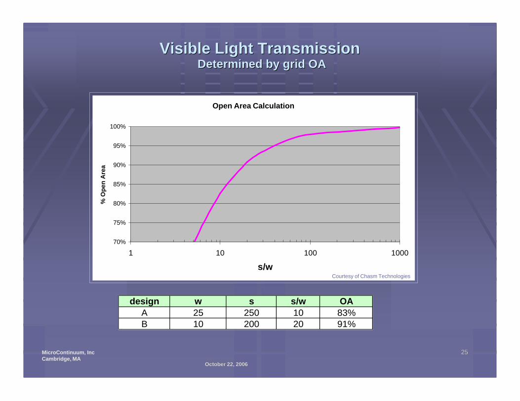
Visible Light TransmissionVisible Light TransmissionDetermined by grid OADetermined by grid OA
s
design w s s/w OA
A 25 250 10 83%B 10 200 20 91%
w
Open Area Calculation
70%
75%
80%
85%
90%
95%
100%
1 10 100 1000
s/w
% O
pen
Are
a
Courtesy of Chasm Technologies
October 22, 2006October 22, 2006
2626MicroContinuum, IncCambridge, MA
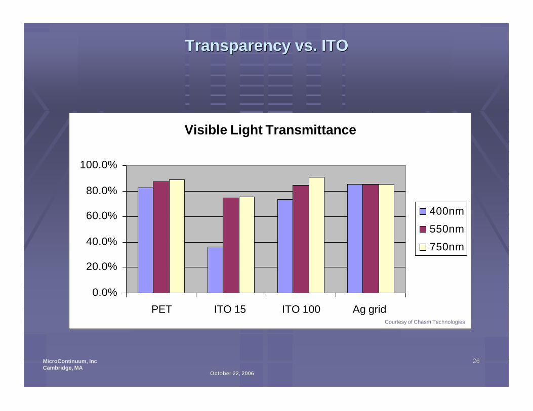
Transparency vs. ITO Transparency vs. ITO
Visible Light Transmittance
0.0%
20.0%
40.0%
60.0%
80.0%
100.0%
PET ITO 15 ITO 100 Ag grid
400nm
550nm
750nm
Courtesy of Chasm Technologies
October 22, 2006October 22, 2006
2727MicroContinuum, IncCambridge, MA
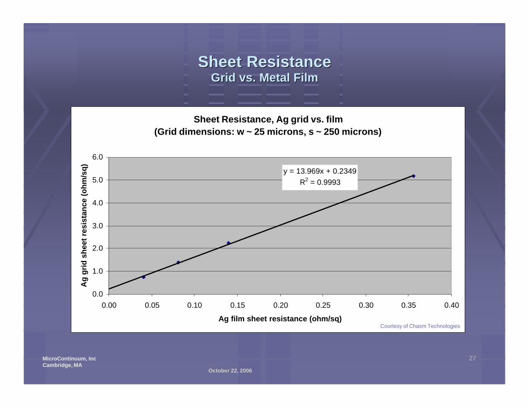
Sheet ResistanceSheet ResistanceGrid vs. Metal FilmGrid vs. Metal Film
Sheet Resistance, Ag grid vs. film
(Grid dimensions: w ~ 25 microns, s ~ 250 microns)
y = 13.969x + 0.2349
R2 = 0.9993
0.0
1.0
2.0
3.0
4.0
5.0
6.0
0.00 0.05 0.10 0.15 0.20 0.25 0.30 0.35 0.40
Ag film sheet resistance (ohm/sq)
Ag
gri
d s
he
et
res
ista
nc
e (
oh
m/s
q)
Sheet Resistance, Ag grid vs. film
(Grid dimensions: w ~ 25 microns, s ~ 250 microns)
y = 13.969x + 0.2349
R2 = 0.9993
0.0
1.0
2.0
3.0
4.0
5.0
6.0
0.00 0.05 0.10 0.15 0.20 0.25 0.30 0.35 0.40
Ag film sheet resistance (ohm/sq)
Ag
gri
d s
he
et
resis
tan
ce
(o
hm
/sq
)
Courtesy of Chasm Technologies
October 22, 2006October 22, 2006
2828MicroContinuum, IncCambridge, MA
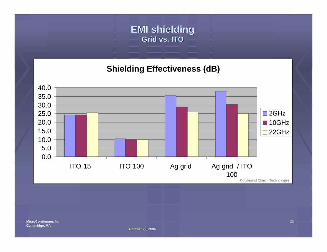
EMI shieldingEMI shieldingGrid vs. ITOGrid vs. ITO
Shielding Effectiveness (dB)
0.0
5.010.0
15.0
20.0
25.0
30.0
35.0
40.0
ITO 15 ITO 100 Ag grid Ag grid / ITO
100
2GHz
10GHz
22GHz
Courtesy of Chasm Technologies
October 22, 2006October 22, 2006
2929MicroContinuum, IncCambridge, MA
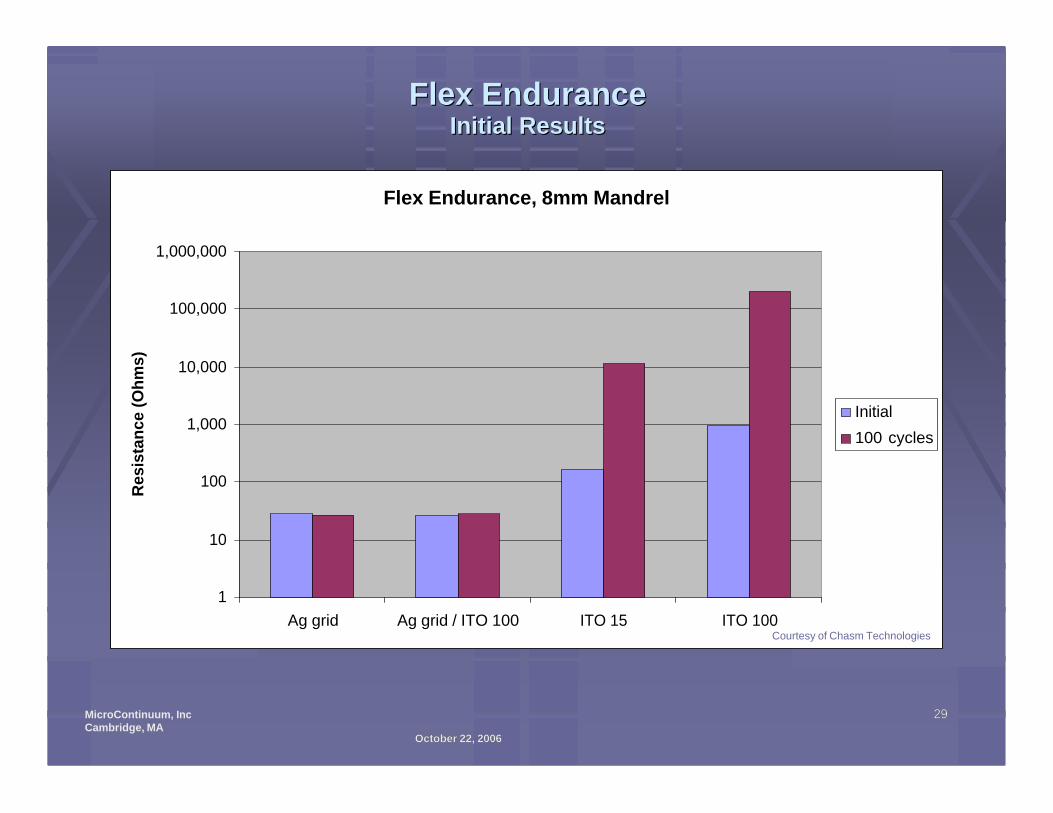
Flex EnduranceFlex EnduranceInitial ResultsInitial Results
Flex Endurance, 8mm Mandrel
1
10
100
1,000
10,000
100,000
1,000,000
Ag grid Ag grid / ITO 100 ITO 15 ITO 100
Resis
tan
ce (
Oh
ms)
Initial
100 cycles
Courtesy of Chasm Technologies
October 22, 2006October 22, 2006
3030MicroContinuum, IncCambridge, MA
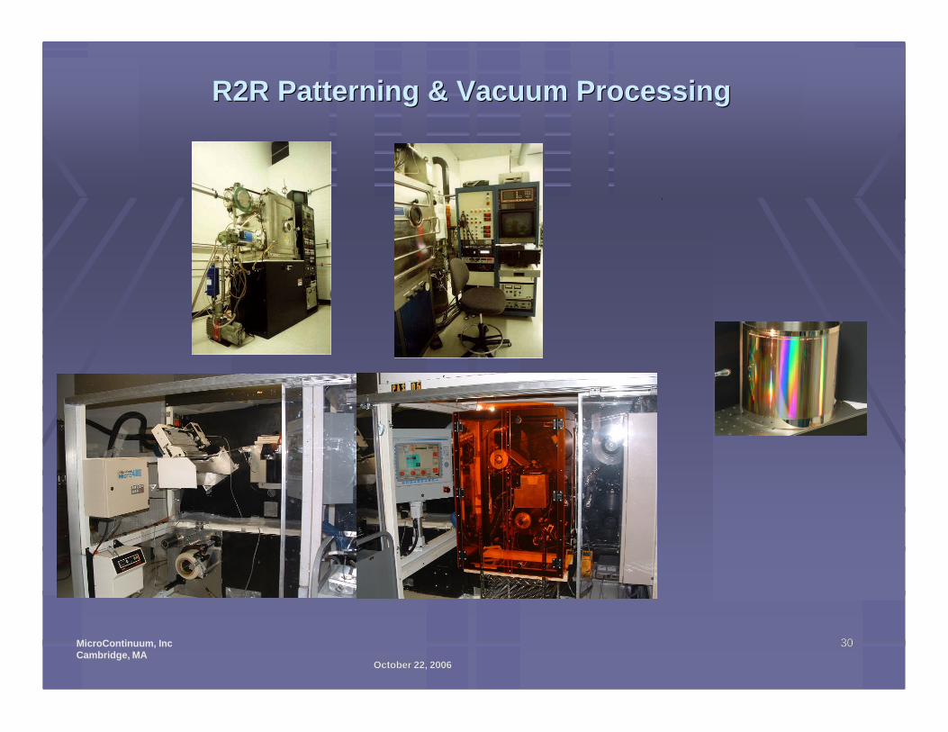
R2R Patterning & Vacuum Processing R2R Patterning & Vacuum Processing
October 22, 2006October 22, 2006
3131MicroContinuum, IncCambridge, MA
AcknowlegdmentsAcknowlegdments
USDC USDC Chasm TechnologiesChasm Technologies