Embed Size (px)
Citation preview

Novel Optical Transmitters for High
Speed Optical Networks
John O’Carroll
B.Eng., M.Eng.
A thesis submitted in part fulfilment of the
requirements for the Degree of
Doctor of Philosophy (Ph.D)
to the
Dublin City University
Faculty of Engineering & Computing
School of Electronic Engineering
Supervisor: Prof. Liam P. Barry
January 2013


i
Declaration
I hereby certify that this material, which I now submit for assessment on the
programme of study leading to the award of Doctor of Philosophy (Ph.D) is entirely
my own work, that I have exercised reasonable care to ensure that the work is
original, and does not to the best of my knowledge breach any law of copyright, and
has not been taken from the work of others save and to the extent that such work has
been cited and acknowledged within the text of my work.
Signed: ________________________
ID No.: 58104321
Date: ___________

ii
Abstract
The objective of this thesis is to investigate the performance of novel optical
transmitter lasers for use in high speed optical networks. The laser technology
considered is the discrete mode laser diode (DMLD) which is designed to achieve
single wavelength operation by etching features on the surface of the ridge
waveguide. This leads to a simplified manufacturing process by eliminating the
regrowth step used in conventional approaches, presenting an economic approach to
high volume manufacture of semiconductor lasers. Two application areas are
investigated in this work.
The bit rate in next generation access networks is moving to 10 Gbit/s. This work
characterises the performance of DMLDs designed for high speed operation with the
objective of identifying the limitations and improving performance to meet the
specifications for uncooled operation at 10 Gbit/s.
With the deployment of advanced modulation formats the phase noise of the laser
source has become an important parameter, particularly for higher order formats.
DMLDs were developed for narrow linewidth operation. The linewidth of these
devices was characterised and a value as low as 70 kHz was demonstrated.
Transmission experiments were also carried out using a coherent transmission test
bed and the performance achieve is compared with that of an external cavity laser.

iii
Acknowledgement
First and foremost, I would like to thank my supervisor Prof. Liam Barry for his
excellent supervision and for providing me with the opportunity to work on this
project. I would particularly like to thank Liam for his assistance in helping me
balance my commitments to DCU and Eblana, without which the completion of this
work would not have been possible.
Thanks also to Dr. Prince Anandarajah for his help over the years with setups and
organising equipment.
I would also like to thank past and present members of the group for help with
various setups over the years, particularly Prince, Tam, Barry, Frank and Sylwester.
I am also grateful to Eblana Photonics for the support the company has given me
over the course of this project, and I would like to thank the following:
Dr. James O’Gorman, for first proposing that I pursue this project with DCU.
Dr. Richard Phelan, for his insight into laser design; the many discussions over the
years have been invaluable.
Dr. Brian Kelly, for the many useful discussions, particularly relating to device
processing.
Dr. Diarmuid Byrne, for his advice on laser modelling.
Jim Somers, for making time available to carry out work relating to this project and
also for granting me a leave of absence to complete this thesis.
Also, Rob, Diarmuid, Richard and Brian for reading through this thesis and
providing useful feedback.
I would like to thank Radan Slavík at the ORC in the University of Southampton for
performing a power spectral density measurement on a laser, which is presented in
this thesis.
Finally, I would like thank my parents for their constant love and support. To my
brothers Eamon and Mike, thanks for all the encouragement.

iv

v
Contents
Declaration i
Abstract ii
Acknowledgement iii
List of Figures x
List of Tables xv
Acronyms xvi
1 Introduction 1
References 4
2 High speed optical communication networks 5
2.1 The growth in capacity 5
2.2 Optical networks 7
2.2.1 Long haul network 7
2.2.2 Core network 8
2.2.3 Metropolitan area network 9
2.2.4 Access network 9
2.2.5 Meeting future capacity needs 12
2.3 Modulation formats 13
2.3.1 Non-return-to-zero on/off keying 13

vi
2.3.1.1 Direct modulation 14
2.3.1.2 External modulation 15
2.3.2 Return-to-zero on/off keying 17
2.3.3 Advanced modulation formats 18
2.3.3.1 Binary differential phase shift keying 19
2.3.3.2 Quadrature phase shift keying 20
2.3.3.3 16-ary quadrature amplitude modulation 21
2.3.3.4 Detection of phase modulation formats 23
2.3.3.5 Linewidth requirements for advanced
modulation formats 25
2.4 Conclusion 28
References 28
3 Single mode lasers 35
3.1 Semiconductor materials 35
3.1.1 Multi-quantum well structures 37
3.2 Carrier and photon confinement 39
3.2.1 Transverse confinement 39
3.2.2 Lateral confinement 40
3.2.2.1 Gain guided structures 40
3.2.2.2 Index guided structures 41
3.3 Lasers for optical communications 42
3.3.1 Fabry Pérot lasers 44
3.3.2 Single mode lasers 45

vii
3.3.2.1 Distributed feedback laser 45
3.3.2.2 Distributed Bragg reflector laser 46
3.3.2.3 Vertical cavity surface emitting laser 47
3.3.2.4 External cavity laser 49
3.4 Single mode laser characteristics 52
3.4.1 Light-current characteristic 52
3.4.2 Side mode suppression ratio 53
3.4.3 Relative intensity noise 54
3.4.4 Modulation bandwidth 54
3.4.5 Linewidth 56
3.5 Conclusion 60
References 60
4 Discrete mode laser diodes 63
4.1 Single mode operation in a discrete mode laser diode 63
4.1.1 Theory of operation 64
4.2 Characterisation of DMLDs for fibre optic communications 72
4.2.1 Directly modulated lasers 73
4.2.1.1 1310 nm window 74
4.2.1.2 1550 nm window 79
4.2.2 Narrow linewidth lasers 82
4.2.3 Higher power lasers 94
4.3 Conclusion 97
References 99
viii
5 Direct modulation of discrete mode laser diodes 103
5.1 1310 nm DMLD 103
5.2 1550 nm DMLD 109
5.2.1 10 Gbit/s transmission at 1550 nm with
dispersion compensation 112
5.3 Discussion 114
5.4 Conclusion 117
References 118
6 Characterisation of discrete mode laser diodes
in advanced modulation format systems 119
6.1 Experimental setup 120
6.1.1 Digital signal processing 122
6.2 QPSK 124
6.2.1 QPSK self-homodyne receiver 125
6.2.2 QPSK heterodyne receiver 129
6.3 16-QAM 131
6.3.1 16-QAM self-homodyne receiver 132
6.3.2 16-QAM heterodyne receiver 134
6.4 Discussion 136
6.5 Conclusion 139
References 140

ix
7 Conclusion and future work 143
7.1 Conclusion 143
7.2 Future work 146
References 148
Appendix A: List of Publications Arising From This Work 149
A.1 Referred Journals 149
A.2 Conference Papers 152

x
List of Figures
Fig. 2.1 North American internet traffic by year. Pg. 6
Fig. 2.2. Number of fibre connections as a percentage of broadband connections
among OECD countries reporting fibre subscribers, as of June 2011. Pg. 11
Fig. 2.3. Light current characteristic of a laser, showing the idealised conversion of a
current pulse train to an optical pulse train under direct modulation. Pg. 15
Fig. 2.4. MZM (a) modulator structure and (b) transmission characteristic. Pg. 17
Fig. 2.5 (a) IQ modulator structure and (b) QPSK constellation diagram. Pg. 21
Fig. 2.6 Theoretical BER versus OSNR for phase modulation formats. Pg. 22
Fig. 2.7 Optical quadrature front end. Pg. 24
Fig. 3.1. Schematic of an in-plane ridge waveguide laser diode. Pg. 38
Fig. 3.2. MQW (a) energy band diagram and (b) density of states (solid line), also
shown is the density of states for a bulk structure (dashed line). Pg. 38
Fig. 3.3. Ridge waveguide (a) SEM image showing the front facet view and (b) a
picture of the top-surface of a fabricated laser diode chip. Pg. 42
Fig. 3.4. Buried hetrostructure with regrown semi-insulating semiconductor
material. Pg. 42
Fig. 3.5. Optical spectrum from (a) an FP laser and (b) a single mode laser. Pg. 43
Fig. 3.6. Schematic for (a) standard DFB and (b) quarter wave shifted DFB. Pg. 46
Fig. 3.7. Schematic of a DBR laser. Pg. 47
Fig. 3.8. Cross section of a VCSEL. Pg. 49
Fig. 3.9. Schematic of an ECL based on a PLC platform. Pg. 50
Fig. 3.10. ECL in (a) Littrow configuration and (b) Littman configuration. Pg. 51
Fig. 3.11. ECL using thermally tuneable silicon etalon filters for wavelength
selection. Pg. 52
Fig. 3.12. Modulation response of a single mode laser, with an extracted 3 dB
bandwidth of 13 GHz. Pg. 56
Fig. 3.13. Simulated linewidth versus inverse power. Pg. 58

xi
Fig. 3.14. Simulated linewidth versus cavity length. Pg. 59
Fig. 3.15. Simulated linewidth versus front facet reflectivity. Pg. 59
Fig. 4.1. (a) SEM image of 2μm wide ridge waveguide with etched slots. The slot
width is 1 μm and the spacing between the slots is 4 μm in this example. (b)
Illustration of slot reflection and transmission for N slots. Pg. 66
Fig. 4.2. Overlapped power reflection versus wavelength simulation results, for slot
spacing ranging from 3.31 μm to 3.46 μm. Pg. 68
Fig. 4.3. Overlapped power reflection versus wavelength simulation results, for slot
numbers ranging from 10 to 30. Pg. 69
Fig. 4.4. Simulated reflection peak wavelength versus refractive index. Pg. 70
Fig. 4.5. Spectra measured for DMLDs with operating wavelengths of (a) 684 nm,
(b) 779 nm, (c) 1276 nm, (d) 1393 nm, (e) 1645 nm, and (f) 2002 nm. Pg. 71
Fig. 4.6. Single mode wavelength emission spectrum of a DMLD fabricated on
InGaAs/AlAsSb Quantum Cascade materials showing an SMSR of 25dB, also
overlapped is the broad emission spectrum from an FP laser from the
same wafer. Pg. 72
Fig. 4.7. 1310 nm DMLD L-I plots over the range -40 ˚C ≤ T ≤ 97 ˚C. Pg. 75
Fig. 4.8. Measured emission spectrum of a DMLD biased for 5 mW emission,
showing a high SMSR of 45 dB. Inset: Typical multimode emission spectrum of an
FP laser fabricated on the same wafer (i.e. a DMLD fabricated without any index
perturbing features) under the equivalent operating conditions. Pg. 76
Fig. 4.9. 1310 nm DMLD optical spectra measured over the range
-40 ˚C ≤ T ≤ 95 ˚C. Pg. 76
Fig. 4.10. Far field measurement at 25 ˚C and 85 ˚C, in (a) the parallel direction and
in (b) the perpendicular direction. Pg. 77
Fig. 4.11. 1310 nm DMLD L-I characteristic measured at 25 ˚C. Pg. 78
Fig. 4.12. 1310 nm DMLD optical spectra measured at 25 ˚C. Pg. 78
Fig. 4.13. Modulation response of a 1310 nm DM laser showing the modulation
bandwidth over current ranging from 20 mA to 60 mA. Pg. 79
Fig. 4.14. 1550 nm DMLD module L-I plots over the range
-20 ˚C ≤ T ≤ 95 ˚C. Pg. 80
Fig. 4.15. 1550 nm DMLD optical spectra measured over the range
-20 ˚C ≤ T ≤ 95 ˚C. Pg. 80
Fig. 4.16. Far field measurement at 25 ˚C and 85 ˚C, in (a) the parallel direction and
in (b) the perpendicular direction. Pg. 81
Fig 4.17. Relaxation oscillation frequency versus √ over the range
-20 ˚C ≤ T ≤ 85 ˚C. Pg. 82
xii
Fig. 4.18. 1550 nm DMLD module L-I plots over the range 0 ˚C ≤ T ≤ 85 ˚C. Pg. 83
Fig. 4.19. 1550 nm DMLD measured optical spectra over the range
-10 ˚C ≤ T ≤ 110 ˚C. Pg. 84
Fig. 4.20. Peak wavelength and SMSR versus temperature. Pg. 84
Fig. 4.21. Peak wavelength and SMSR versus bias current at 25 ˚C. Pg. 84
Fig. 4.22. Delayed self-heterodyne experimental set-up. Pg. 85
Fig. 4.23. Extracted linewidth versus optical power at T = 25 ˚C. Pg. 86
Fig. 4.24. D-SH spectrum at I = 300mA with Lorentzian fit
linewidth = 138 kHz. Pg. 87
Fig. 4.25. Linewidth versus temperature at constant power in the fibre of 4 mW and
also at a constant bias current of 250 mA. Pg. 87
Fig. 4.26. 1550 nm DMLD module L-I plots measured at 0 ˚C, 20 ˚C
and 50 ˚C. Pg. 88
Fig. 4.27. 1550 nm DMLD measured optical spectra over the range
-5 ˚C ≤ T ≤ 50 ˚C. Pg. 89
Fig. 4.28. Peak wavelength and SMSR versus bias current at 20 ˚C. Pg. 89
Fig. 4.29. Peak wavelength and SMSR versus bias current at 20 ˚C. Pg. 89
Fig. 4.30. Extracted linewidth versus optical power at T = 20 ˚C. Pg. 90
Fig. 4.31. D-SH spectrum at I = 400 mA with Lorentzian fit
linewidth = 70 kHz. Pg. 91
Fig. 4.32. Linewidth versus temperature at a constant bias current of 300 mA. Pg. 91
Fig. 4.33. Measurement set-up for frequency noise PSD measurement based on
frequency-to-amplitude converter. Pg. 93
Fig. 4.34. Overlapped frequency noise spectrum measured at (a) 200 mA, 300 mA
and 400mA, over a frequency range of 0.1 kHz to 10 MHz and (b) 300 mA and
400mA, over a frequency range of 1 kHz to 100 kHz and showing extracted
linewidth values. Pg. 94
Fig. 4.35. Overlapped L-I plot measured ex-facet over the range
0 ˚C ≤ T ≤ 85 ˚C. Pg. 95
Fig. 4.36. 1550 nm DMLD measured optical spectra over the range
0 ˚C ≤ T ≤ 95 ˚C. Pg. 96
Fig. 4.37. Peak wavelength and SMSR versus temperature. Pg. 96
Fig. 4.38 D-SH spectrum at I = 300mA with Lorentzian fit
linewidth = 194 kHz. Pg. 97
Fig. 5.1. Overlapped optical spectra for a 1310 nm DMLD at 25 ˚C, with modulation
current on and off, measured at a wavelength span of (a) 40 nm and (b) 1 nm. Pg.105

xiii
Fig. 5.2. Experimental setup for 10 Gbit/s transmission experiments at
1310 nm. Pg. 106
Fig. 5.3. Back-to-back eye diagram for a 1310 nm DMLD directly modulated at 10
Gbit/s at 25 ˚C. Pg. 106
Fig. 5.4. BER versus received optical power, measured back-to-back and after
transmission through 10 km and 22 km of SSMF for a 1310 nm DMLD directly
modulated at 10 Gbit/s at 25 ˚C. Pg. 106
Fig. 5.5. Eye diagram for a 1310 nm FP directly modulated at 10 Gbit/s, at (a) 25 ˚C
and (b) 85 ˚C. Pg. 108
Fig. 5.6. BER versus received optical power, back-to-back and after transmission
through 1 km and 2 km of SSMF for a 1310 nm FP directly modulated at 10 Gbit/s at
(a) 25 ˚C and (b) 85 ˚C. Pg. 108
Fig. 5.7. Eye diagram for a 1310 nm FP TOSA directly modulated at 10 Gbit/s, at
room temperature. Pg. 109
Fig. 5.8. Overlapped optical spectra for a 1550 nm DMLD at 25 ˚C, with modulation
current on and off, measured at a span of (a) 40 nm (resolution 0.02 nm) and (b) 3
nm (0.16 pm resolution). Pg. 110
Fig. 5.9. Experimental setup for 10 Gbit/s transmission experiments at
1550 nm. Pg. 111
Fig. 5.10. Back-to-back eye diagram for a 1550 nm DMLD directly modulated at 10
Gbit/s at 25 ˚C. Pg. 111
Fig. 5.11. BER versus received optical power, measured back-to-back and after
transmission through 10 km and 20 km of SSMF for a 1550 nm DMLD directly
modulated at 10 Gbit/s at 25 ˚C. Pg. 112
Fig. 5.12. BER versus received optical power with dispersion pre-compensation of -
681 ps/nm, measured back-to-back and after transmission through 10, 22, 37, 49 and
60 km of SSMF. Inset: table listing the power penalties at the transmission distances
measured. Pg. 113
Fig. 5.13. BER versus received optical power measured after transmission through
37 km of SSMF, using dispersion pre-compensation and post compensation. Pg. 114
Fig. 6.1. Coherent transmission setup, QPSK or 16-QAM modulation can be
generated by applying the appropriate electrical drive signals to the IQ modulator. By
switching between a decorrelated portion of the TX laser, or a separate LO laser, the
receiver can be setup as a self-homodyne or heterodyne receiver. Pg. 121
Fig. 6.2. Transmitted QPSK eye diagram measured at (a) 10 Gbaud, (b) 5 Gbaud and
(c) 2.5 Gbaud, using a DMLD with a linewidth of 190 kHz as the TX laser. Pg. 125
xiv
Fig. 6.3. EVM versus received power measured with the QPSK setup using a self-
homodyne receiver at 10 Gbaud, 5 Gbaud and 2.5 Gbaud, for a DMLD with a
linewidth of 190 kHz and an ECL with a linewidth of 100 kHz. Pg. 127
Fig. 6.4. EVM versus received power measured with the QPSK setup using a self-
homodyne receiver at 10 Gbaud, for a DMLD with the linewidth of 190 kHz and a
DFB with a linewidth of 1.5 MHz, and also at 2.5 Gbaud for a DMLD with linewidth
of 190 kHz and a DMLD with a linewidth of 460 kHz. Pg. 128
Fig. 6.5. Constellation diagrams measured with the QPSK setup using a self-
homodyne receiver at 2.5 Gbaud and a received power of -20 dBm for (a) ECL,
linewidth 100 kHz, (b) DMLD, linewidth 190 kHz, (c) DMLD, linewidth 460 kHz
and (d) DFB, linewidth 1.5 MHz. Pg. 128
Fig. 6.6. EVM versus received power measured with the QPSK setup using a
heterodyne receiver at 10 Gbaud, 5 Gbaud and 2.5 Gbaud, for DMLDs as the TX and
LO lasers with linewidths of 190 kHz and 120 kHz, respectively. Also plotted an
ECL with a linewidth of 100 kHz measured with a self-homodyne receiver
setup. Pg. 130
Fig. 6.7. Constellation diagrams measured with the QPSK setup using a heterodyne
receiver at (a) 10 Gbaud, (b) 5 Gbaud and (c) 2.5 Gbaud, at a received power of -20
dBm for DMLDs as the TX and LO lasers with linewidths of 190 kHz and 120 kHz,
respectively. Pg. 131
Fig. 6.8. Transmitted 16-QAM eye diagram measured at 5 Gbaud, using a DMLD
with a linewidth of 190 kHz as the TX laser. Pg. 131
Fig. 6.9. EVM versus received power measured with the 16-QAM setup using a self-
homodyne receiver at 5 Gbaud, for an ECL with a linewidth of 100 kHz, a DMLD
with a linewidth of 80 kHz, a DMLD with a linewidth of 190 kHz and a DMLD with
a linewidth of 300 kHz. Pg. 133
Fig. 6.10. Constellation diagrams measured with the 16-QAM setup using a self-
homodyne receiver at 5 Gbaud and a received power of -23 dBm for (a) ECL,
linewidth 100 kHz, (b) DMLD, linewidth 80 kHz, (c) DMLD, linewidth 190 kHz and
(d) DMLD, linewidth 300 kHz. Pg. 133
Fig. 6.11. EVM versus received power measured with the 16-QAM setup using a
heterodyne receiver at 5 Gbaud for the following: DMLD TX linewidth 190 kHz,
ECL LO linewidth 100 kHz; DMLD TX linewidth 190 kHz, DMLD LO linewidth 85
kHz; and DMLD TX linewidth 80 kHz, ECL LO linewidth 100 kHz. Pg. 135
Fig. 6.12. Constellation diagrams measured using the 16-QAM setup with a
heterodyne receiver at 5 Gbaud and a received power of -23 dBm for (a) DMLD TX
linewidth 190 kHz, ECL LO linewidth 100 kHz, (b) DMLD TX linewidth 190 kHz,
DMLD LO linewidth 85 kHz and (c) DMLD TX linewidth 80 kHz, ECL LO
linewidth 100 kHz. Pg. 135

xv
List of Tables
Table 2.1. Transmission speeds for DSL modem technologies. Pg. 11
Table 2.2. Linewidth bit rate products and maximum combined linewidth
requirements for phase estimation methods. Pg. 28
Table. 3.1. Parameters used in linewidth simulation. Pg. 58
Table 4.1. Summary of the 1310 nm DMLD characteristics measured over the
temperature range -40 ˚C ≤ T ≤ 85 ˚C. Pg. 98
Table 4.2. Summary of the 1550 nm DMLD characteristics measured over the
temperature range -20 ˚C ≤ T ≤ 85 ˚C. Pg. 98
Table 4.3. Summary of low linewidth DMLDs design parameters and the
corresponding minimum linewidth values demonstrated. Pg. 99
Table 5.1. Summary of the transmission experiment results at 1310 nm. Pg. 117
Table 5.2. Summary of the transmission experiment results at 1550 nm. Pg. 118
Table. 6.1. Specifications for components used in coherent transmission
setup. Pg. 123
Table. 6.2. EVM values measured using the QPSK setup at 10 Gbaud, 5 Gbaud and
2.5 Gbaud, for an ECL and a DMLD measured using the self-homodyne receiver
setup and two DMLDs measured using the heterodyne receiver setup. Pg. 140
Table. 6.3. EVM values measured using the 16-QAM setup at 5 Gbaud, for an ECL
and a DMLD measured using the self-homodyne receiver setup, two DMLDs
measured using the heterodyne receiver setup and a DMLD as the TX and an ECL as
the LO measured using the heterodyne receiver setup. Pg. 140

xvi
Acronyms
AR
Anti-reflection
ASE
Amplified spontaneous emission
ASK
Amplitude shift keying
ATM
Asynchronous transfer mode
AWG
Arbitrary waveform generator
BER
Bit error ratio
CATV
Community access television
CW
Continuous wave
DBPSK
Binary differential phase shift keying
DBR
Distributed Bragg reflector
DCF
Dispersion compensating fibre
DFB
Distributed feedback
DMLD
Discrete mode laser diode
DP-QPSK
Dual-polarisation quadrature phase shift keying
D-SH
Delayed self-heterodyne
DSL
Digital subscriber line
DSP
Digital signal processing
DWDM
Dense wavelength division multiplexing
EAM
Electroabsorption modulator
ECL
External Cavity laser
EDFA
Erbium doped fibre amplifier
EML
Externally modulated laser
EVM
Error vector magnitude
FEC
Forward error correction
FFT
Fast Fourier transform
FIBE
Focused ion beam etching
FP
Fabry Pérot
xvii
FTIR
Fourier transform infrared
FTTC
Fibre-to-the-curb
FTTH
Fibre-to-the-home
HR
High reflectivity
ICP
Inductive coupled plasma
IEEE
Institute of electrical and electronics engineers
IQ
In-phase quadrature
ISI
Inter-symbol interference
ITU
International telecommunications union
L-I
Light-current
LiNbO3
Lithium niobate
LO
Local oscillator
LPE
Liquid phase epitaxy
LR
Low reflectivity
MAN
Metropolitan area network
MBE
Molecular beam epitaxy
MEMs
Micro-electro-mechanical system
MOCVD
Metal-organic chemical vapour deposition
MPLS
Multiprotocol label switching
MQW
Multi-quantum well
MZI
Mach-Zehnder interferometer
MZM
Mach-Zehnder modulator
NRZ-OOK
Non-return-to-zero on/off keying
OADM
Optical add-drop multiplexer
OECD
Organisation for Economic Co-operation and Development
OEO
Optical-electrical-optical
OMVPE
Organometallic vapour-phase epitaxy
OOK
On/off keying
OPLL
optical phase locked loop
OSA
Optical spectrum analyser
OSNR
Optical signal to noise ratio
PIC
Photonic integrated circuit
PLC
Planer lightwave circuit

xviii
PM
Polarization maintaining
PON
Passive optical network
p-p
Peak-to-peak
PRBS
Pseudo random binary sequence
PSK
Phase shift keying
QAM
Quadrature amplitude modulation
QPSK
Quadrature phase shift keying
RF Radio frequency
RIN
Relative intensity noise
rms
Root-mean-square
ROADM
Reconfigurable optical add-drop multiplexer
RZ-OOK Return-to-zero on/off keying
SCH
Separate confinement heterostructure
SDH
Synchronous digital hierarchy
SEM
Scanning electron microscope
SGDBR
Sampled grating distributed Bragg reflector
SMSR
Side mode suppression ratio
SNR
Signal to noise ratio
SNRb
Signal to noise ratio per bit
SOA
Semiconductor optical amplifier
SONET
Synchronous optical networking
SQW
Single quantum well
SSMF
Standard single mode fibre
T
Temperature
TEC
Thermoelectric cooler
TX
Transmitter
VCSEL
Vertical cavity surface emitting laser
VDSL2
Very high data rate digital subscriber line 2
VNA
Vector network analyser
WDM
Wavelength division multiplexing

1
Chapter 1
Introduction
Delivering high speed broadband connections to a country’s population is recognised
as an important driver for economic growth in knowledge based economies as well
as being of benefit to society as a whole. Targets set by the European Union state that
by 2020 all Europeans should have access to connection speeds of at least 30 Mbit/s
and 50 %, or more, of European households should have subscriptions above
100 Mbit/s [1]. Also, all member states are required to put in place a broadband
strategy to meet these goals. The Irish government recently announced its strategy,
with objectives to deliver by 2015, 70 to 100 Mbit/s to more than half the population,
at least 40 Mbit/s to a further 20 to 35 %, centred around smaller towns and villages,
and a minimum of 30 Mbit/s throughout the country, even in remote locations [2].
The United States has also set out a broadband strategy, with a goal of having 100
million households with access to connection speeds of 100 Mbit/s by 2020 [3]. In
order to meet these targets existing network infrastructure will have to be upgraded.
Operators will have to ensure that the connection to the customer has sufficient
bandwidth to deliver these higher speeds, and that the network as a whole has
sufficient capacity to handle the cumulative increase in data traffic.

2
Increasing the capacity of fibre optic networks will require continued development of
these systems, and their constituent components. This thesis primarily looks at one
component, the semiconductor laser diode, and considers a novel approach for
producing single mode lasers called a discrete mode laser diode (DMLD). This
approach offers the potential for high-volume, low-cost fabrication of single-mode
lasers as no regrowth is required. Two application areas are considered, directly
modulated transmitters and a continuous wave (CW) source for use with advanced
modulation formats where external modulation is used. Throughout this thesis,
unless otherwise stated, single mode refers to single longitudinal mode.
Key results from the work carried out towards this thesis are:
Demonstration of 10 Gbit/s operation using DMLDs at both 1310 nm and
1550 nm.
Demonstration of a linewidth as low as 70 kHz from a DMLD designed for
low linewidth operation.
Demonstration of a low linewidth DMLD exhibiting a wide operating
temperature range. At a constant power of 4 mW a maximum linewidth of
235 kHz was measured at 85 ˚C, and a minimum value of 212 kHz was
measured at 25 ˚C, corresponding to a variation in the linewidth of only 23
kHz over the range 0 to 85 ˚C.
Low linewidth DMLDs were characterised in a coherent transmission setup
employing quadrature phase shift keying (QPSK) and 16-ary quadrature
amplitude modulation (16-QAM). The performance achieved in the setup
using DMLDs was compared with that achieved using an external cavity laser
(ECL) and similar performance was achieved at baud rates as low as
2.5 Gbaud and 5 Gbaud for QPSK and 16-QAM, respectively. These were the

3
first experimental demonstrations where DMLDs were used as the transmitter
(TX) or local oscillator (LO) in a coherent transmission setup where either of
these modulation formats were employed.
This thesis is structured as follows:
Chapter 2 gives an overview of optical communication networks. The growth in
capacity and issues related to maintaining growth levels to meet future bandwidth
demands are discussed. The final section in the chapter looks at optical modulation
formats and the technologies used to modulate the optical carrier.
Chapter 3 gives an overview of semiconductor laser diodes, and looks at the
materials and structures used in their fabrication. Approaches used to achieve single
mode operation are discussed, along with important characteristics for devices
targeted at optical communication applications.
Chapter 4 gives an overview of DMLDs and describes how single mode operation is
achieved in this type of laser. A simplified model is presented which describes how
the single mode characteristics of the device can be controlled by modifying design
parameters in this device. Static characterisation results are presented for two types
of device, the first targeted at direct modulation applications and the second at
optical coherent communications.
Chapter 5 looks at the performance of DMLDs under direct modulation at a bit rate
of 10 Gbit/s. Results are presented for lasers operating in both the 1310 nm and
1550 nm wavelength windows, and includes the transmission performance over
single mode fibre.
Chapter 6 looks at the performance of DMLDs designed for narrow linewidth
emission in a test bed employing advanced modulation formats. Two modulation
4
formats are considered; QPSK and 16-QAM, and the performance achieved using
low linewidth DMLDs and an ECL is compared.
Chapter 7 presents a brief conclusion to the thesis and discusses the potential for
future work in this area.
Finally, Appendix A presents a list of the author’s publications arising from this
work.
References
[1] European Commission, “European Broadband: investing in digitally driven growth,”
2010. [Online]. Available:
http://ec.europa.eu/information_society/activities/broadband/docs/bb_communication.
pdf.
[2] Department of Communications, Energy and Natural Resources, “Delivering a
Connected Society - A National Broadband Plan for Ireland,” 30 August 2012.
[Online]. Available: http://www.dcenr.gov.ie/NR/rdonlyres/1EA7B477-741B-4B74-
A08E-6350135C32D2/0/NBP.pdf.
[3] US, Federal Communications commission, “National broadband plan, Chapter 2 Goals
for a high performance America,” 16 March 2010. [Online]. Available:
http://download.broadband.gov/plan/national-broadband-plan-chapter-2-goals-for-
high-performance-america.pdf.

5
Chapter 2
High speed optical
communication networks
This chapter gives an overview of optical communication networks. It looks at the
growth in capacity of these networks and how growth levels can be maintained to
meet future capacity needs. Optical modulation formats and the technologies used to
modulate the optical carrier are discussed.
2.1 The growth in capacity
Since fibre optics were first introduced to telecommunication networks the growth in
capacity has been remarkable. Fibre has led to cheaper voice calls, lower
maintenance costs [1] and provided a high capacity and low cost data network that
has been a key ingredient in the development of the internet [2]. Over the last 20
years, the internet has evolved from a primarily text based medium to a multimedia
platform used in the office, home and on mobile devices. Applications such as video
on demand, video conferencing, online gaming and cloud computing are a reality,
and will undoubtedly see continued development in the coming years. Internet video

6
traffic alone now accounts for almost 50 % of consumer internet traffic and this is
forecast to grow to 62 % by 2015 [3]. Getting to this point has been made possible by
continuous technical innovation. One example is the erbium doped fibre amplifier
(EDFA), which enabled transmission over long distances without optical-electrical-
optical (OEO) conversion. Significantly, the wide optical bandwidth of the EDFA
meant that multiple wavelength channels could be amplified simultaneously, making
possible the cost effective deployment of wavelength division multiplexing (WDM)
technology. The timing of its commercial deployment in the mid 90’s was also
significant as it coincided with the commercial deployment of the internet. Fig. 2.1
shows the internet traffic per month for North America from 1990 to 2015 [3, 4];
between 1994 and 1996 the internet traffic increased by over 90 fold coinciding with
the introduction of WDM. Since then, growth in internet traffic has been relentless,
facilitated by WDM and other technological advances in fibre optics.
Fig. 2.1 North American internet traffic by year.
With the increased popularity of mobile devices, such as smart phones, tablet
computers and portable gaming consoles, worldwide mobile data traffic grew by
133 % in 2011 and growth rates of 110 % and 78 % are forecast for 2012 and 2014,
respectively, resembling the growth patterns seen in fixed line traffic in the late
7
nineties and early two thousands [5]. It is forecast that global IP traffic will grow to
almost 1 Zettabyte per year by 2015, a fourfold increase from 2010 levels [3],
providing an impetus for continued innovation in communication systems.
2.2 Optical networks
An optical network consists of a number of interconnected sub-networks, each with
their own architecture designed to perform specific functions within the network.
The technological challenges that need to be overcome to grow capacity vary
according to network type.
2.2.1 Long haul network
Long haul networks are used to connect countries and continents and can be made up
of terrestrial links, covering distances of a few thousands km, and ultra-long haul
submarine links, covering distances from 6,000 to 12,000 km [6]. Modern submarine
cables are designed to transmit bit rates in excess of 1 Tbit/s per fibre [7], and
because of the distances involved the technical obstacles can be quite challenging.
However, they are essentially point-to-point links allowing a certain degree of
flexibility in their design, and design parameters such as amplifier position and
dispersion compensation can be optimised to maximise performance. With the
development of forward error correction (FEC) an increased number of channels can
be transmitted per fibre using tighter WDM grid spacing and because of their point-
to-point architecture submarine cables don’t necessarily have to comply with the ITU
grid [8].

8
2.2.2 Core network
The core is the backbone of a national fibre optic network, connecting several
regional networks together. The connection point in the regional networks is called a
node. The core also connects with long haul networks to extend global
interconnectivity between national domains [6]. Data from many users is
amalgamated and transported through different nodes in the network. The links
between individual nodes are point-to-point WDM links, and each node can be
connected to several nodes in the network, producing an interconnected network with
a mesh structure. When transmitting an optical signal through the network it can be
routed through several nodes through switching operations which direct the optical
signal to the correct destination in the network. In legacy networks the signals were
routed by OEO cross connects, where the optical signals entering the node are
converted to the electrical domain and routing performed electronically before
retransmitting the optical signals to the appropriate destination. The preferred option,
where possible, is to route the signals in the optical domain. A significant step
towards all optical routing was the development of the optical add-drop multiplexer
(OADM), which allowed signals not destined for a node to by-pass it and remain in
the optical domain, therefore significantly reducing the cost and size of the OEO
cross-connects required in each node [9]. The development of tuneable transponders,
wavelength selective switches, and reconfigurable OADMs (ROADMs) have
increased the flexibility of all-optical networks and have contributed to all-optical
solutions permeating today’s core networks [10].

9
2.2.3 Metropolitan area network
The metropolitan area network (MAN) is the fibre transport network and covers a
geographical area which can range from several blocks of buildings to entire cities
[11]; it typically has a ring topology spanning distances up to 250 km. The MAN
provides interconnectivity between the core and the access network, and must
support a large range of technologies such as synchronous digital
hierarchy/synchronous optical networking (SDH)/(SONET), dense wavelength
division multiplexing (DWDM), asynchronous transfer mode (ATM), multiprotocol
label switching (MPLS) and Ethernet, all of which may be operating at different data
rates. A further requirement is that it needs to be reconfigurable, and this is achieved
using ROADMs, allowing dynamic and flexible node-to-node connections [6].
2.2.4 Access network
The access network connects the customer to the rest of the network; it is often
referred to as the last mile although typical distances can be up to 20 km.
Traditionally, the access network was a copper network infrastructure. However,
since the beginning of this century fibre has seen growing commercial importance
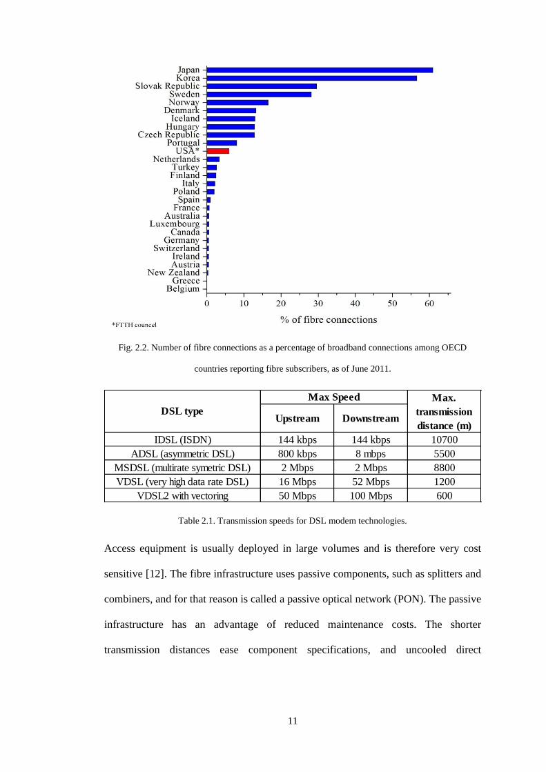
[12]. The level of penetration of fibre in access varies between countries and this is
shown in Fig. 2.2 which plots data gathered by the Organisation for Economic Co-
operation and Development (OECD) for the number of fibre connections as a
percentage of total broadband connections among OECD countries reporting fibre
subscribers as of June 2011 [13]. The OECD data did not give a figure for the USA;
however, a survey carried out on behalf of the fibre-to-the-home (FTTH) council
found that 6 % of homes were connected with 18 % of homes passed for FTTH as of
March 2011 [14]. In Japan, the county with highest percentage of fibre broadband

10
connections, FTTH became the leading access technology in September 2008 [15].
For a considerable period of time, barriers to FTTH deployment were the high cost of
fibre optic components and the lack of applications to take advantage of the high
bandwidth offered by FTTH [12]. Therefore, when upgrading existing copper
infrastructure most operators opted against providing FTTH, instead opting for an
incremental upgrade by retrofitting existing infrastructure, which in general meant
extending the reach of fibre in the field. In fibre-to-the-curb (FTTC) the fibre
connection is provided to the curb of a community and is converted to an electrical
signal which is then transported to the customer via the existing copper
infrastructure. The copper wiring is either twisted pair, in the case of a telecoms
operator, or coaxial cable, for community access television (CATV) operators. For
the twisted pair case, digital subscriber line (DSL) modems have been developed
which can achieve relatively high connection speeds, and by decreasing the
transmission distance over copper these can be increased further. In very high data
rate DSL2 (VDSL2) using vectoring, which is a technique to cancel far end cross talk
between adjacent copper wires in the bundle, it is possible to achieve downstream bit
rates in excess of 100 Mbit/s over short distances of 600 m or less [16, 17]. Table 2.1
summarises the maximum transmission speeds achievable and the corresponding
maximum transmission distances for various DSL technologies [12, 16]. CATV
systems can achieve even higher bit rates as coaxial cable is a better high frequency
transmission medium than twisted pair and with the latest DOCSIS 3.0 modems
downstream data rates of 160 Mbps are possible [12]. In recent years the cost of
optical components has come down significantly, and this, coupled with the
projected capacity demand, make FTTH an attractive solution for operators.
11
Fig. 2.2. Number of fibre connections as a percentage of broadband connections among OECD
countries reporting fibre subscribers, as of June 2011.
Table 2.1. Transmission speeds for DSL modem technologies.
Access equipment is usually deployed in large volumes and is therefore very cost
sensitive [12]. The fibre infrastructure uses passive components, such as splitters and
combiners, and for that reason is called a passive optical network (PON). The passive
infrastructure has an advantage of reduced maintenance costs. The shorter
transmission distances ease component specifications, and uncooled direct
Upstream Downstream
IDSL (ISDN) 144 kbps 144 kbps 10700
ADSL (asymmetric DSL) 800 kbps 8 mbps 5500
MSDSL (multirate symetric DSL) 2 Mbps 2 Mbps 8800
VDSL (very high data rate DSL) 16 Mbps 52 Mbps 1200
VDSL2 with vectoring 50 Mbps 100 Mbps 600
DSL type
Max Speed Max.
transmission
distance (m)

12
modulation transmitter lasers can be used allowing devices with lower cost packages,
such as TO-cans, to be used.
2.2.5 Meeting future capacity needs
The level of service provided to the customer can be compromised if the network as
a whole has insufficient capacity or if a bottleneck is created in any part of the
network. Existing networks will need to be upgraded to meet forecast capacity needs.
In the core, the approach adopted is to replace conventional on/off keying (OOK)
with advanced modulation formats to increase spectral efficiency in WDM systems.
This approach is now a commercial reality with the deployment of 40G and 100G
systems. For 100G, and certain implementations of 40G, dual-polarisation quadrature
phase shift keying (DP-QPSK) is being employed. In the next evolution of these
systems higher order modulation formats have the potential to significantly increase
capacity; a further advantage of these new formats is that increased capacity can be
achieved while maintaining the baud rate at levels which allow the use of readily
available lower cost electro-optics and high speed electronics [18, 19]. An advantage
of DP-QPSK 100G systems is compatibility with 50 GHz DWDM channel spacing
[20]. By moving to dual-polarisation 16-QAM the bit rate could be doubled to
224 Gbit/s, while maintaining the same baud rate and wavelength channel spacing as
current 100G systems [21, 22]. To move to 400G, and beyond, channel spacing will
be an issue and the adaption of a flexible wavelength grid may be necessary [23, 24],
although this will have significant cost implications as the optics in current systems
are designed for a 50 GHz grid. Coherent technology could also be applied to
metropolitan [25] and access networks [26] to meet future bandwidth demands in
those applications.

13
Limitations in the capacity of the access network can create a bottleneck. The
primary limitation is the proximity of the fibre network to the end customer, the
solution is to bring fibre closer to the customer, ideally to the home or failing that as
close as possible so as to maximise the data rate using DSL technology. As capacity
demands increase, standardisation bodies such as the international
telecommunications union (ITU) and the institute of electrical and electronics
engineers (IEEE) have put in place standards to increase the bit rate from
1 Gbit/s (IEEE) and 2.5 Gbit/s (ITU) to 10 Gbit/s [27, 28]. Another solution being
investigated is WDM PON; utilising WDM technology would lead to a significant
increase in capacity, but also a substantial increase in cost as splitters and combiners
would have to be replaced with arrayed waveguide grating multiplexers and de-
multiplexers. The monetary benefits of the various approaches will determine which
approach is taken; a possible situation may develop where 10 Gbit/s PON is initially
used for residential applications while WDM-PON is investigated for business or
bandwidth intensive backhaul [29].
2.3 Modulation formats
2.3.1 Non-return-to-zero on/off keying
Non-return-to-zero OOK (NRZ-OOK) is the most widely used modulation format in
today’s fibre optic networks. The primary reason for this is that its simplicity makes
it cost effective. While advanced modulation formats are being adopted for long haul
applications NRZ-OOK will still be used in MAN and access networks for the
foreseeable future. In NRZ-OOK the information is encoded in the intensity of the
optical signal and recovered through direct detection at the receiver. In the simplest
14
case logic ‘1’ is transmitted by light with intensity P1 and logic ‘0’ is transmitted by
the absence of light. In practical implementations when transmitting logic ‘0’, a low
level of light with intensity P0 is still transmitted. The extinction ratio describes the
modulation efficiency and is defined by the ratio of P1 & P0, measured in decibels:
Extinction ratio = 10 × log(P1 / P0) (dB) (2.1)
The format can be generated through direct modulation of the laser’s current or by
modulating a continuous wave laser source using an external modulator. The method
used is determined by the specification of the end application.
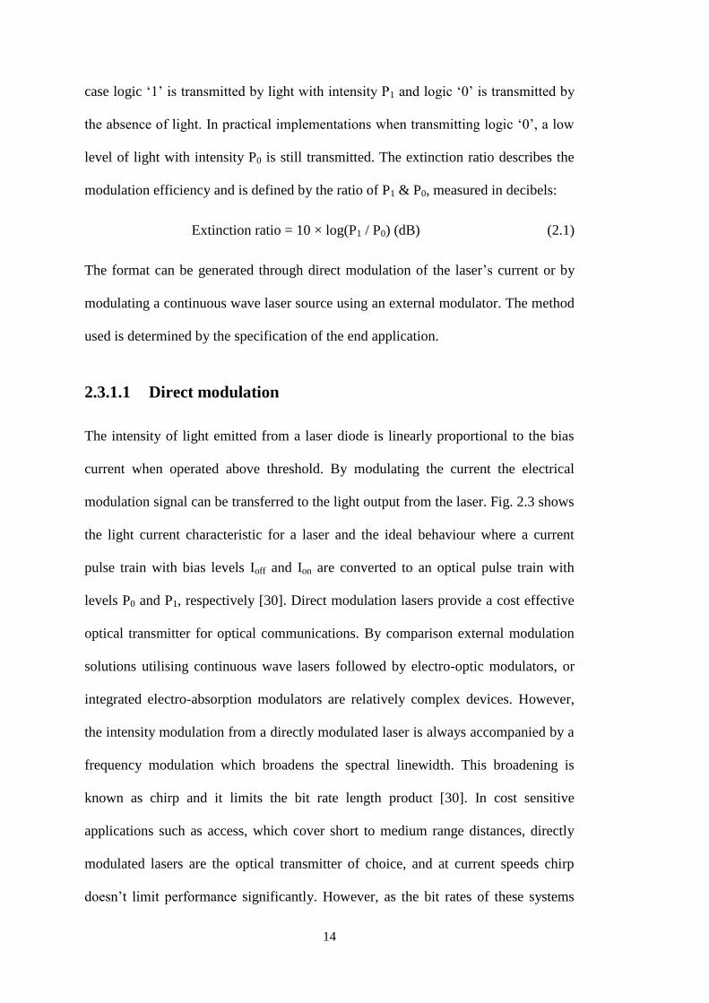
2.3.1.1 Direct modulation
The intensity of light emitted from a laser diode is linearly proportional to the bias
current when operated above threshold. By modulating the current the electrical
modulation signal can be transferred to the light output from the laser. Fig. 2.3 shows
the light current characteristic for a laser and the ideal behaviour where a current
pulse train with bias levels Ioff and Ion are converted to an optical pulse train with
levels P0 and P1, respectively [30]. Direct modulation lasers provide a cost effective
optical transmitter for optical communications. By comparison external modulation
solutions utilising continuous wave lasers followed by electro-optic modulators, or
integrated electro-absorption modulators are relatively complex devices. However,
the intensity modulation from a directly modulated laser is always accompanied by a
frequency modulation which broadens the spectral linewidth. This broadening is
known as chirp and it limits the bit rate length product [30]. In cost sensitive
applications such as access, which cover short to medium range distances, directly
modulated lasers are the optical transmitter of choice, and at current speeds chirp
doesn’t limit performance significantly. However, as the bit rates of these systems

15
increase from 2.5 Gbit/s to 10 Gbit/s their application is likely to be limited to
transmitters in the 1310 nm window, while more advanced transmitter structures
with lower chirp are likely to be the preferred option for 1550 nm, where dispersion
in standard single mode fibre (SSMF) is higher.
Fig. 2.3. Light current characteristic of a laser, showing the idealised conversion of a current pulse
train to an optical pulse train under direct modulation.
2.3.1.2 External modulation
In structure an electroabsorption modulator (EAM) is quite similar to a laser. The
device has a waveguide structure and is fabricated from PIN semiconductor
materials. It is designed to be transparent to laser light at a particular wavelength,
with the level of transparency controlled by the application of an electric field. When
no voltage is applied the bandgap is designed to be wide enough so as to be
transparent to the laser light. Applying a reverse bias voltage decreases the bandgap
16
causing the laser light to be absorbed. The reverse bias is typically in the region of
2 V and extinction ratios of ≈ 10 dB can be achieved. Discrete devices are not
normally used, instead EAMs are monolithically integrated with a single mode laser
to form a device called an externally modulated laser (EML). In order to achieve
high extinction ratios the peak wavelength of the laser needs to be detuned from the
modulator material in order to design the optimum bandgap separation. This can be
achieved through separate growth stages for both devices [31]. In comparison to
directly modulated lasers EMLs can achieve much longer transmission distances due
to lower chirp, at the expense of a more complex device structure. At 1550 nm EMLs
operating at 10 Gbit/s are available for operation at distances of up to 80 km. Devices
operating at 40 Gbit/s are available for short reach applications up to 2 km, with
research devices operating up to 80 Gbit/s demonstrated [8].
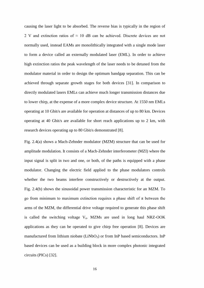
Fig. 2.4(a) shows a Mach-Zehnder modulator (MZM) structure that can be used for
amplitude modulation. It consists of a Mach-Zehnder interferometer (MZI) where the
input signal is split in two and one, or both, of the paths is equipped with a phase
modulator. Changing the electric field applied to the phase modulators controls
whether the two beams interfere constructively or destructively at the output.
Fig. 2.4(b) shows the sinusoidal power transmission characteristic for an MZM. To
go from minimum to maximum extinction requires a phase shift of π between the
arms of the MZM, the differential drive voltage required to generate this phase shift
is called the switching voltage Vπ. MZMs are used in long haul NRZ-OOK
applications as they can be operated to give chirp free operation [8]. Devices are
manufactured from lithium niobate (LiNbO3) or from InP based semiconductors. InP
based devices can be used as a building block in more complex photonic integrated
circuits (PICs) [32].

17
(a) (b)
Fig. 2.4. MZM (a) modulator structure and (b) transmission characteristic.
2.3.2 Return-to-zero on/off keying
In NRZ-OOK when transmitting logic ‘1’ light with power P1 is transmitted for the
duration of the symbol period. In return-to-zero OOK (RZ-OOK) modulation P1 is
transmitted for a fraction (such as ⅓ or ½) of the symbol period and the optical
power goes to P0 within each symbol period. RZ pulses can be generated either
electrically or in the optical domain through the use of an additional modulator called
a pulse carver. The former is feasible up to 10 Gbit/s whereas the latter has to be
employed at bit higher bit rates up to 40 Gbit/s and beyond. The shorter pulse
duration reduces the impact of inter-symbol interference (ISI), leading to a reduction
of 1 to 3dB in the optical signal to noise ratio (OSNR) required to achieve a given bit
error rate (BER) when compared to NRZ. This made RZ formats attractive for long
haul 10 Gbit/s submarine links. However, the introduction of forward error
correction FEC revitalised interest in NRZ as a lower BER could be tolerated. The
narrower spectral width of NRZ also enables the denser packing of channels and
therefore an increased capacity [8].

18
2.3.3 Advanced modulation formats
New network roll outs can be designed for optimum performance using spectrally
efficient modulation formats and optimally designed fibre links. Because of the
capital expense involved in deploying fibre optic links the main focus is developing
technologies that can be deployed in the upgrade of existing infrastructure. Existing
systems are mainly based on WDM intensity-modulation direct-detection (IM-DD)
and operate at 10 Gbit/s per channel; it is not feasible to simply increase the bit rate
of these systems as transmission impairments, such as dispersion and nonlinear
effects, have more of an impact at higher bit rates. Instead the solution that has been
adopted by the industry is to migrate to advanced modulation formats which have a
higher tolerance to transmission impairments. Conventional IM-DD systems use only
the amplitude to transmit information, whereas, advanced modulation formats
primarily use phase to modulate the optical carrier enabling multiple bits to be
transmitted per symbol [33]. In conjunction with phase, the amplitude and, or,
polarisation can be exploited for modulation enabling even higher spectral
efficiencies. While it is possible to transmit multiple bits per symbol using multi-
level amplitude shift keying (ASK), the OSNR requirements make this impractical
except for short link applications [33]. Increasing the number of bits transmitted per
symbol increases the spectral efficiency for a given bit rate, it also reduces the baud
rate to levels which allow the use of readily available lower cost electro-optics and
high speed electronics [18, 19]. In higher order modulation formats the number of
bits transmitted per symbol, m, is related to the number of symbols M by:
(2.2)
19
In the reception of optical signals the BER is used as a figure of merit for the quality
of a received signal. In characterising a received optical signal the BER is measured
versus a system parameter which describes the received signal. The signal can be
characterised by measuring the optical power, or by measuring the ratio of signal
power to noise power. Two parameters commonly used are the signal to noise ratio
(SNR) and the OSNR. The SNR is an electrical parameter and is the ratio of the
received signal power versus electrical noise power and the OSNR is the ratio of
optical signal power to optical noise power. The SNR is related to OSNR by [33]:
(2.3)
Where is the energy per symbol, is the noise power spectral density, is
an optical reference bandwidth and is the symbol rate. Practically, a value of
12.5 GHz is normally used for unless a specific value is specified [34]. The SNR
can also be quoted as SNR per bit (SNRb) and is defined as [35]:
(2.4)
2.3.3.1 Binary differential phase shift keying
Binary differential phase shift keying (DBPSK) is a binary modulation format where
the phase of adjacent bits is used to encode the information; logic ‘1’ is represented
by π phase change in the optical carrier and logic ‘0’ is represented by the absence of
a phase change [36]. The phase of the optical carrier is modulated using either an
electro-optic phase modulator or, preferably in terms of performance, an MZM.
Advantages of the format include a higher tolerance to nonlinear effects in fibre
transmission and up to 3 dB improved receiver sensitivity, when compared to OOK.
Apart from performance advantages, a contributing factor to its deployment in
20
commercial systems was that it could be implemented with a relatively small
increase in system complexity, when compared to existing OOK systems [33]. By
placing an optical interferometer, with a one bit delay in one of its arms, in front of
the photodiode, variations in phase are converted to variations in amplitude that can
be directly detected. The modulation format is a strong candidate for 40 Gbit/s
systems, particularly long haul links [7]. A distance of 9420 km over legacy
submarine fibre has been reported using dual polarisation BPSK and coherent
detection [37].
2.3.3.2 Quadrature phase shift keying
Multi-level modulation formats can achieve higher spectral efficiency than binary
formats. QPSK is a multilevel format that has been extensively studied and chosen
for use in state of the art commercial 100 G systems [18, 19]. Four phase states, each
separated by 90˚, are used to encode the data onto the optical carrier. Two bits per
symbol are transmitted achieving double the spectral efficiency of binary formats.
QPSK is normally generated using an in-phase quadrature (IQ) modulator. The IQ
modulator is a nested MZM structure with a second phase modulator on one, or both,
of the arms to introduce a phase shift of π/2 as shown in Fig. 2.5 (a). QPSK can also
be generated using two phase modulators in series, where the first introduces a phase
shift of 0 or π and the second 0 or π/2 [33]. Fig. 2.5 (b) shows the constellation for a
QPSK signal. The spectral efficiency can be increased further through the use of
more phase levels with 8PSK and 16PSK being the next logical steps. Increasing the
number of phase states decreases the separation between the constellation points, and
therefore increasing the SNR requirement for these formats.

21
(a) (b)
Fig. 2.5 (a) IQ modulator structure and (b) QPSK constellation diagram.
2.3.3.3 16-ary quadrature amplitude modulation
Quadrature amplitude modulation (QAM) employs both the amplitude and phase to
modulate the optical carrier. In higher order formats, employing phase modulation
with constant amplitude, increasing the number of symbols decreases the separation
between constellation points. The separation between constellation points can be
increased using amplitude in combination with phase to map each point. Increasing
the distance between adjoining constellation points makes it easier to identify the
correct symbol at the receiver and thereby reduces the SNR requirement. The BER
versus OSNR can be estimated for M-ary PSK and M-ary QAM from (2.5) and (2.6),
respectively [33, 38].
( )
(√ (
)) (2.5)
( )
(
√ ) (√
( ) ) (2.6)
Fig. 2.6 plots BER versus OSNR obtained using (2.5) and (2.6) at a bit rate of
40 Gbit/s. To achieve a BER of 1 × 10⁻³
an OSNR of 17 dB is required for 16-PSK

22
compared to 12.6 dB for 16-QAM. Also shown is the OSNR requirement for higher
order QAM formats. The higher OSNR requirements of 16-QAM, compared to
QPSK, will make achieving ultra-long transmission distances challenging.
Transmission distances of 1000 km are possible in systems using 16-QAM operating
at a bit rate of 200 Gbit/s, this compares to distances of 2500 km in 100 Gbit/s
systems where QPSK is used [39]. For 32-QAM, 64-QAM and above, the increase in
the required OSNR will limit the achievable transmission distance using these
formats even further. Therefore, the design of future systems may involve comprise
between capacity and distance, with higher order modulation formats being preferred
for shorter distances. Improving the overall noise performance of optical links can
extend the transmission distance. One potential option is to decrease the spacing
between optical amplifiers in the optical link in order to reduce the overall system
noise [19].
Fig. 2.6 Theoretical BER versus OSNR for phase modulation formats.
16-QAM can be generated using an IQ modulator where multi-level signals
(quaternary) are applied to the I and Q inputs. The electrical requirements for the
drive signals can be simplified to binary levels at the expense of increasing the
complexity of the optical modulator [33].

23
2.3.3.4 Detection of phase modulation formats
When a phase modulated optical signal is applied to a conventional square law
detector the phase information is lost. In order to detect the signal the optical phase
information needs to be converted to an optical intensity which can then be detected
using conventional detectors. When two optical signals are combined in a 3 dB
coupler, depending on the phase difference, they either interfere constructively or
destructively at the output. To demodulate the received signal a phase reference is
required at the receiver. This can be generated using a delayed version of the
received signal or using a second optical source to act as a phase reference; these
configurations are termed self-coherent and coherent, respectively. In DBPSK an
MZI with a one bit delay on one arm is placed before the photodetector. When the
paths are recombined at the interferometer’s output coupler, two adjacent bits either
interfere constructively or destructively depending on the phase difference between
them, which is 0 or π. To achieve the 3 dB improvement in sensitivity possible using
DBPSK the constructive and destructive ports of the interferometer are applied to a
balanced detector. This configuration can be extended for use with higher order
modulation formats. However, as the order increases the complexity of the optics
required also increases. For M-ary PSK as the value of M increases the SNR penalty
also increases, differential detection also incurs an additional penalty with increasing
M, termed the differential-detection penalty. From values of approximately 0.4 dB
and 2 dB for DBPSK and DQPSK, respectively, the differential-detection penalty
approaches 3 dB as M increases further; for M ≥ 8 this limits its application to
systems with sufficiently high SNR [8].
Coherent detection can be used to extract all the information relating to an optical
signal (amplitude, frequency, phase and polarisation) by taking the product of the
24
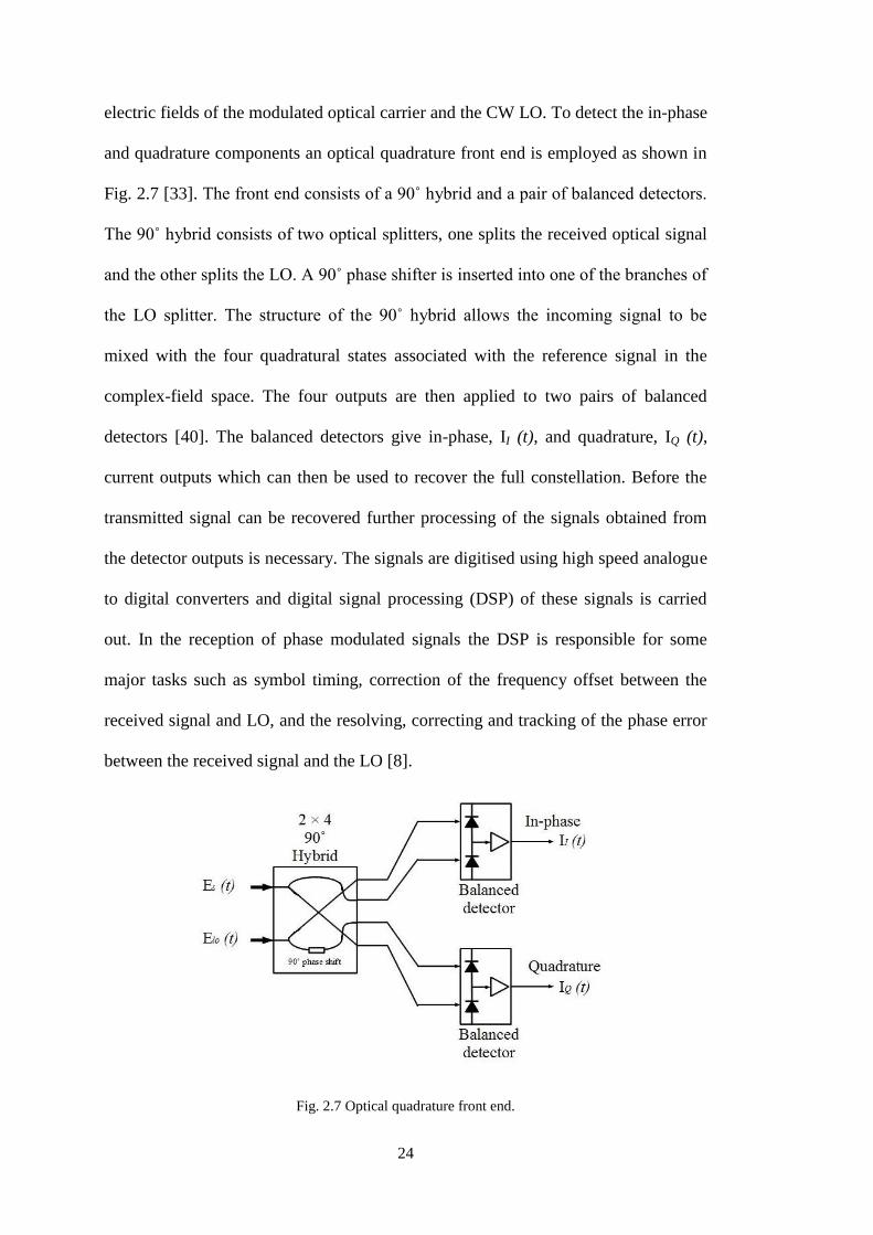
electric fields of the modulated optical carrier and the CW LO. To detect the in-phase
and quadrature components an optical quadrature front end is employed as shown in
Fig. 2.7 [33]. The front end consists of a 90˚ hybrid and a pair of balanced detectors.
The 90˚ hybrid consists of two optical splitters, one splits the received optical signal
and the other splits the LO. A 90˚ phase shifter is inserted into one of the branches of
the LO splitter. The structure of the 90˚ hybrid allows the incoming signal to be
mixed with the four quadratural states associated with the reference signal in the
complex-field space. The four outputs are then applied to two pairs of balanced
detectors [40]. The balanced detectors give in-phase, II (t), and quadrature, IQ (t),
current outputs which can then be used to recover the full constellation. Before the
transmitted signal can be recovered further processing of the signals obtained from
the detector outputs is necessary. The signals are digitised using high speed analogue
to digital converters and digital signal processing (DSP) of these signals is carried
out. In the reception of phase modulated signals the DSP is responsible for some
major tasks such as symbol timing, correction of the frequency offset between the
received signal and LO, and the resolving, correcting and tracking of the phase error
between the received signal and the LO [8].
Fig. 2.7 Optical quadrature front end.
25
Similar to OOK, FEC can be performed in DSP but because coherent receivers
recover the full information relating to the optical field it enables other functions to
be carried out using DSP including compensation of chromatic dispersion and
polarisation mode dispersion. Compensating for dispersion in DSP as opposed to
using dispersion compensating fibre (DCF) reduces the latency of the network which
would be beneficial for delay sensitive applications [41]. It also improves the
received OSNR as DCF introduces loss to the link. There is also the potential to
compensate for fibre nonlinear effects in DSP, however, the algorithms are quite
complex and require a lot of processing power which has implications for power
consumption.
2.3.3.5 Linewidth requirements for advanced modulation formats
In coherent detection the optimum performance would be achieved in an ideal case
where the TX laser and LO laser are aligned in frequency and synchronised in phase.
The phase noise of a laser can be characterised as a random walk process. In an
observation time interval, τ, the phase, ( ), exhibits a random phase change of
( ) ( ) ( ). The phase difference between and is Gaussian
distributed with zero mean and the phase variance, ⟨ ( )⟩, is proportional to the
product of the observation time interval and the combined linewidth of the TX
laser, , and the LO laser, ,: ⟨ ( )⟩ ( ) . The
observation time interval can be related to the symbol interval in a coherent system.
An increase in the linewidth or symbol interval leads to an increase in the phase
variance [18, 42], which is why lower baud rate systems have more stringent
linewidth requirements. In phase modulated formats increased phase variance causes
broadening of the constellation points. As the separation between the constellation

26
points decreases for higher order modulation formats any broadening of the
constellation points leads to an increased possibility of an error occurring. The
sensitivity of the receiver to this phase variance is dependent on how phase
synchronisation is achieved. Prior to the development of DSP, the linewidth was a
critical parameter as the baud rates were lower and phase synchronisation was
carried out using hardware based optical phase locked loops (OPLLs). Implementing
an OPLL in hardware is not trivial and the performance achievable is very sensitive
to the loop delay. In a QPSK experimental setup operating at 40 Gbit/s an OPLL
with a loop delay of 12 ns had a linewidth requirement of 24 kHz [33]. Integrated
solutions could enable optimisation of the OPLL design by minimising delays in the
circuit. Modern coherent receivers implement algorithms to estimate the phase in
DSP and this has eased the linewidth requirements. Two widely used algorithms
include a decision feedback loop where a phase estimate is extracted from a number
of symbols and feedforward schemes where the phase modulation is removed by
raising it to the Mth
power. Table 2.2 summarises calculated combined linewidth, ,
requirements at a bit rate of 10 Gbit/s and bit period Tb for an OPLL [43], a feedback
algorithm utilising a digital phase locked loop (DPLL) [35] and four implementations
of feedforward based digital carrier phase estimation algorithms [35, 42, 44, 45].
Feedforward algorithms can tolerate higher linewidths than feedback algorithms
based on DPLLs. The feedforward algorithm proposed in [44] reduces the linewidth
requirements for 16-QAM to levels that can be achieved by standard single mode
lasers such as a DFB. However, for higher order QAM formats, M > 16 and
depending on the baud rate, lasers with linewidths of 100 kHz and below will still be
necessary even when feedforward are used. In [45] the optimum phase noise estimate
is obtained by applying a finite Wiener filter to reduce the effect of

27
shot-noise/amplifier noise, allowing a combined linewidth of 8 MHz to be tolerated
at 10 Gbit/s for QPSK. While feedforward circuits can be designed to implement
filter circuits in memory and can tolerate large linewidths, this comes at the expense
of significantly more gates in the ASIC circuit and therefore increased footprint size
and increased power consumption [18]. Feedback algorithms, while less tolerant to
linewidth have the advantage of being simpler to implement allowing simplified
ASIC circuits to be used, thereby reducing the footprint of the ASIC and importantly
reducing power consumption. The availability of low linewidth laser sources allows
simplified algorithms to be used in the receivers of systems.
In the reception of a coherent signal a cycle slip occurs when the phase estimate is
incorrect by 90˚ in formats with square constellations. Contributing sources of cycle
slips include laser phase noise, non-linear effects and amplified spontaneous
emission (ASE) noise [46]. Differential encoding can be employed to prevent
catastrophic failures due to cycle slips. In comparison to uncoded QPSK, differential
encoded QPSK has an equivalent OSNR penalty of 1.1 dB at a BER of 1 × 10⁻²
[47].
Avoiding the use of differential encoding is advantageous in that it allows high
coding gain soft decision FEC to be used, which can extend the reach of coherent
systems. In order to dispense with differential encoding the probability of a cycle slip
needs to be very low, below 10-17
[48]. Reducing the linewidth decreases the
probability of a cycle slip; in [45] using the finite delay Wiener filter phase
estimation algorithm the probability of a cycle slip drops to 10-18
for
∆ν.Tb = 1.1 × 10⁻⁵
. For QPSK operating at a bit rate of 10 Gbit/s this corresponds to a
combined linewidth of 110 kHz as opposed to a value of 8 MHz when cycle slips are
not taken into account. Coherent QPSK systems operating at high bit rates would

28
require low linewidth devices, with combined linewidths below 1 MHz required for a
bit rate of 126 Gbit/s [48].
Table 2.2. Linewidth bit rate products and maximum combined linewidth requirements for phase
estimation methods.
2.4 Conclusion
The continuous growth in capacity of optical networks since they were first deployed
is set to continue. This has provided the impetus for the development of innovative
solutions designed to increase capacity, with the most recent example being the
commercial deployment of coherent systems in the core network. To continue to
meet this challenge will require on-going development of systems across the entire
network and the individual components which make up those systems. The next
chapter reviews the laser sources used in optical networks and discusses the
development of devices for next generation optical systems.
References
[1] R. K. Snelling, “Telecommunications industry rationale for fibre-optics-a business
perspective,” in LEOS Summer Topical on Broadband Analog Optoelectronics:
Devices and Systems,, Monterey, Jul. 1990.
∆ν . Tb
Max. ∆ν,
Tb = 1÷10 Gbit/s∆ν . Tb
Max. ∆ν,
Tb = 1÷10 Gbit/s∆ν . Tb
Max. ∆ν,
Tb = 1÷10 Gbit/s
OPLL 3.5 × 10⁻⁵ 350 kHz 1.3 × 10
-6 13 kHz 1 × 10⁻⁹ 43
Feedback (DPLL) Algorithm 6.9 × 10⁻⁵ 690 kHz 7.9 × 10
-6 79 kHz 1 × 10⁻³ 35
Feedforward Algorithm 1.3 × 10⁻⁴ 1.3 MHz 1.5 × 10
-5 150 kHz 1 × 10⁻³ 35
Feedforward Algorithm 4.8 × 10⁻⁴ 4.8 MHz 6 × 10
-6 60 kHz 6 × 10⁻⁸ 600 Hz 1 × 10
-4 42
Feedforward Algorithm 2.05 × 10⁻⁴ 2.05 MHz 3.5 × 10
-5 350 kHz 6.67 × 10⁻⁶ 67 kHz 3 × 10
-3 44
Feedforward with Wiener filter 8 × 10⁻⁴ 8 MHz 45
Phase synchronisation method Target BER Reference
QPSK 16-QAM 64-QAM

29
[2] A. Gladisch and F. J. Westphal, “Directions of Next Generation Transport Network
Development,” in Optical Fiber Communication Conference (OFC), Los Angeles,
Mar. 2012.
[3] Cisco systems Inc., White paper, “Cisco Visual Networking Index: Forecast and
Methodology, 2010–2015,” 1 June 2011. [Online]. Available:
http://www.cisco.com/en/US/solutions/collateral/ns341/ns525/ns537/ns705/ns827/whi
te_paper_c11-481360.pdf.
[4] R. W. Tkach, “Scaling Optical Communications for the Next Decade and Beyond,”
Bell Labs Technical Journal, vol. 14, no. 4, pp. 3-9, 2010.
[5] Cisco Systems Inc., White Paper, “Cisco Visual Networking Index: Global Mobile
Data Traffic Forecast Update, 2011–2016,” 14 February 2012. [Online]. Available:
http://www.cisco.com/en/US/solutions/collateral/ns341/ns525/ns537/ns705/ns827/whi
te_paper_c11-520862.pdf.
[6] J. M. Senior, Optical Fiber Communications: Principles and Practice, 3rd ed., New
York: Prentice Hall, 2009.
[7] I. Takonori, “Large-capacity Optical Transmission Technologies Supporting the
Optical Submarine Cable System,” NEC Technical Journal, vol. 5, no. 1, pp. 8-12,
2010.
[8] I. P. Kaminow, Optical fiber telecommunications V: B: systems and networks, Boston:
Academic Press, 2008.
[9] M. J. O'Mahony, C. Politi, D. Klonidis, R. Nejabati and D. Simeonidou, “Future
Optical Networks,” Journal of Lightwave Technology, vol. 24, no. 12, pp. 4684-4696,
Dec. 2006.
[10] A. A. Saleh and J. M. Simmons, “All-Optical Networking—Evolution, Benefits,
Challenges, and Future Vision,” Proceedings of the IEEE, vol. 100, no. 5, pp. 1105-
1117, May 2012.
[11] IEEE, “IEEE802: IEEE Standard for Local and Metropolitan Area Networks:
Overview and Architecture,” 7 February 2002. [Online]. Available:
http://standards.ieee.org/getieee802/download/802-2001.pdf.
[12] C. Lam, Passive Optical Networks: Principles and Practice, Boston: Academic Press,
2007.
[13] OECD, “OECD Broadband Portal, Percentage of fibre connections in total broadband
(June 2011),” Jun. 2011. [Online]. Available:
http://www.oecd.org/document/54/0,3746,en_2649_34225_38690102_1_1_1_1,00.ht
ml.
30
[14] FTTH council, “The Growth of Fiber to the Home,” Mar. 2011. [Online]. Available:
http://www.ftthcouncil.org/en/content/the-growth-of-fiber-to-the-home.
[15] K. Tanaka, A. Agata and Y. Horiuchi, “IEEE 802.3av 10G-EPON Standardization and
Its Research and Development Status,” Journal of Lightwave Technology, vol. 28, no.
4, pp. 651-661, Feb. 2010.
[16] V. Oksman, H. Schenk, A. Clausen, J. M. Cioffi, M. Mohseni, G. Ginis, C. Nuzman, J.
Maes, M. Peeters, K. Fisher and P. E. Eriksson, “The ITU-T's new g.vector standard
proliferates 100 mb/s dsl,” IEEE Communications Magazine, vol. 48, no. 10, pp. 140-
148, Oct. 2010.
[17] A. Leshem and L. Youming, “A Low Complexity Linear Precoding Technique for
Next Generation VDSL Downstream Transmission Over Copper,” IEEE Transactions
on Signal Processing, vol. 55, no. 11, pp. 5527-5534 , Nov. 2007.
[18] K. Roberts, M. O'Sullivan, K. T. Wu, H. Sun, A. Awadalla, D. Krause and C. Laperle,
“Performance of Dual-Polarization QPSK for Optical Transport Systems,” Journal of
Lightwave Technology, vol. 27, no. 16, pp. 3546-3559, Aug. 2009.
[19] K. Roberts, D. Beckett, D. Boertjes, J. Berthold and C. Laperle, “100G and beyond
with digital coherent signal processing,” IEEE Communications Magazine, vol. 48, no.
7, pp. 62-69, Jul. 2010.
[20] B. Zhang and S. Khatana, “From lab demo to field trial: Real-time coherent 127 Gb/s
PM-QPSK transmission,” in Photonics Global Conference (PGC), Singapore, Dec.
2010.
[21] A. H. Gnauck, P. J. Winzer, S. Chandrasekhar, X. Liu, B. Zhu and D. W. Peckham,
“10 × 224-Gb/s WDM transmission of 28-Gbaud PDM 16-QAM on a 50-GHz grid
over 1,200 km of fiber,” in Optical Fiber Communication conference (OFC), Los
Angeles, Mar. 2011.
[22] M. S. Alfiad, M. Kuschnerov, S. L. Jansen, T. Wuth, D. van den Borne and H. de
Waardt, “11 x 224-Gb/s POLMUX-RZ-16QAM Transmission Over 670 km of SSMF
With 50-GHz Channel Spacing,” IEEE Photonics Technology Letters, vol. 22, no. 15,
pp. 1150-1152, Aug. 2010.
[23] D. van den Borne, V. Sleiffer, M. S. Alfiad and S. L. Jansen, “Towards 400G and
beyond: How to design the next generation of ultra-high capacity transmission
systems,” in 16th OptoeElectronics and Communications Conference (OECC),
Kaohsiung, Jul. 2011.
[24] V. A. J. M. Sleiffer, D. van den Borne, V. Veljanovski, M. Kuschnerov, M. Hirano, Y.
Yamamoto, T. Sasaki, S. L. Jansen and H. de Waardt, “Transmission of 448-Gb/s
31
dual-carrier POLMUX-16QAM over 1230 km with 5 flexi-grid ROADM passes,” in
Optical Fiber Communication Conference (OFC), Los Angeles, Mar. 2012.
[25] A. Al-Bermani, C. Wordehoff, S. Hoffmann, K. Puntsri, T. Pfau, U. R ckert and R.
No , “Realtime 16-QAM transmission with coherent digital receiver,” in 15th
OptoeElectronics and Communications Conference (OECC), Sapporo, Jul. 2010.
[26] D. Lavery, E. Torrengo and S. Savory, “A long-reach ultra-dense 10 Gbit/s WDM-
PON using a digital coherent receiver,” in Optical Fiber Communication Conference
(OFC), OTuB4, Los Angeles, Mar. 2010.
[27] IEEE, “IEEE 802.3™: ETHERNET,” [Online]. Available:
http://standards.ieee.org/about/get/802/802.3.html.
[28] ITU-T, “10-Gigabit-capable passive optical networks (XG-PON): General
requirements,” Jan. 2010. [Online]. Available:
http://www.itu.int/rec/dologin_pub.asp?lang=e&id=T-REC-G.987.1-201001-I!!PDF-
E&type=items.
[29] C. Ling, S. Dahlfort and D. Hood, “Evolution of PON: 10G-PON and WDM-PON,” in
Communications and Photonics Conference and Exhibition (ACP), Beijing, Dec.
2010.
[30] K. Petermann, Laser Diode Modulation and Noise, London: Kluwer Academic, 1991.
[31] W. Kobayashi, M. Arai, T. Yamanaka, N. Fujiwara, T. Fujisawa, M. Ishikawa, K.
Tsuzuki, Y. Shibata, Y. Kondo and F. Kano, “Wide Temperature Range (-25C–100C)
Operation of a 10-Gb/s 1.55 um Electroabsorption Modulator Integrated DFB Laser
for 80-km SMF Transmission,” IEEE Photonics Technology Letters, vol. 21, no. 15,
pp. 1054-1056, Aug. 2009.
[32] L. A. Coldren, Diode Lasers and Photonic Integrated Circuits, Hoboken: Wiley, 2012.
[33] M. Seimetz, High-Order Modulation for Optical Fiber Transmission, Berlin: Springer,
2009.
[34] R. Hui and M. O'Sullivan, Fiber Optic Measurement Techniques, Burlington: Elsevier
Academic Press, 2009.
[35] E. Ip, A. Pak Tao Lau, D. J. F. Barros and J. M. Kahn, “Coherent detection in optical
fiber systems,” Optics Express, vol. 16, no. 2, pp. 753-791, Jan. 2008.
[36] P. J. Winzer and R. J. Essiambre, “Advanced Modulation Formats for High-Capacity
Optical Transport Networks,” Journal of Lightwave Technology, vol. 24, no. 12, pp.
4711-4728, Dec. 2006.

32
[37] V. A. J. M. Sleiffer, V. Veljanovski, D. van den Borne, J. Capasso, H. Kuluslu, J.
Seixas, V. Schramm, A. Tschersich, R. Nogueira, N. B. Pavlovic, K. Ivarson, S.
Spaelter and H. de Waardt, “45.8 and 125 Gb/s CP-QPSK/CP-BPSK Field Trial Over
Installed Submarine Cable,” Journal of Lightwave Technology, vol. 30, no. 4, pp. 624-
633, Feb. 2012.
[38] J. G. Proakis, Digital communications, Boston: McGraw-Hill, 2001.
[39] M. W. Chbat and S. Spalter, “From 100G to 1000G: Is there a straight road ahead?,” in
European Conference and Exhibition on Optical Communication (ECOC), Torino,
Sept. 2010.
[40] Optoplex Inc., “White paper: Optical Hybrid Enables Next-Generation Optical
Communication,” 2006. [Online]. Available:
http://www.optoplex.com/download/coherent_detection_and_optical_hybrid.pdf.
[41] T. Schmidt, C. Malouin, B. Zhang, R. Saunders, J. Hong and R. Marcoccia, “100G
coherent DWDM transponder module enabling seamless upgrade of long haul optical
transmission systems,” in Optical Fiber Communication conference (OFC), Los
Angeles, Mar. 2010.
[42] M. Seimetz, “Laser Linewidth Limitations for Optical Systems with High-Order
Modulation Employing Feed Forward Digital Carrier Phase Estimation,” in Optical
Fiber communication conference, Los Angeles, Feb. 2008.
[43] E. Ip and J. M. Kahn, “Feedforward Carrier Recovery for Coherent Optical
Communications,” Journal of Lightwave Technology, vol. 25, no. 9, pp. 2675-2692,
Sept. 2007.
[44] T. Pfau, S. Hoffmann and R. Noe, “Hardware-Efficient Coherent Digital Receiver
Concept With Feedforward Carrier Recovery for M-QAM Constellations,” Journal of
Lightwave Technology, vol. 27, no. 8, pp. 989-999, April 2009.
[45] M. G. Taylor, “Phase Estimation Methods for Optical Coherent Detection Using
Digital Signal Processing,” Journal of Lightwave Technology, vol. 27, no. 7, pp. 901-
914, Aprl. 2009.
[46] Y. K. Lize, C. Malouin, E. Ibragimov, B. Zhang and T. Schmidt, “Implementation
challenges of 100G coherent transponders,” in IEEE Photonics Society Summer
Topical Meeting Series, Playa del Carmen, Jul. 2010.
[47] T. Mizuochi, Y. Miyata, K. Kubo, T. Sugihara, K. Onohara and H. Yoshida, “Progress
in soft-decision FEC,” in Optical Fiber Communication Conference (OFC), Los
Angeles, Mar. 2011.

33
[48] E. Ibragimov, B. Zhang, T. J. Schmidt, C. Malouin, N. Fediakine and H. Jiang, “Cycle
slip probability in 100G PM-QPSK systems,” in Optical Fiber Communication
conference (OFC), Los Angeles, Mar. 2010.

34

35
Chapter 3
Single mode lasers
This chapter gives an overview of semiconductor laser diodes and looks at the
materials and structures used in their fabrication. Approaches used to achieve single
mode operation are considered, and characteristics important in optical
communication applications are discussed.
3.1 Semiconductor materials
Semiconductor laser diodes are manufactured from the III/V group of semiconductor
materials. These are direct bandgap materials in that the minimum of the conduction
band and the maximum of the valence band have the same wave vector. A number of
ternary and quaternary compounds have been developed to produce lasers, and
LEDs, emitting light from the visible to the mid-infrared region of the spectrum. The
semiconductor wafers are eptaxially grown by depositing different layers of material
on a substrate. A prerequisite to successfully grow defect-free layers is that the lattice
constants of the deposited layer and the material it is deposited on match. However,
as the lattice constants of different semiconductor materials do not naturally match,
matching has to be created artificially using ternary and quaternary compounds [1].
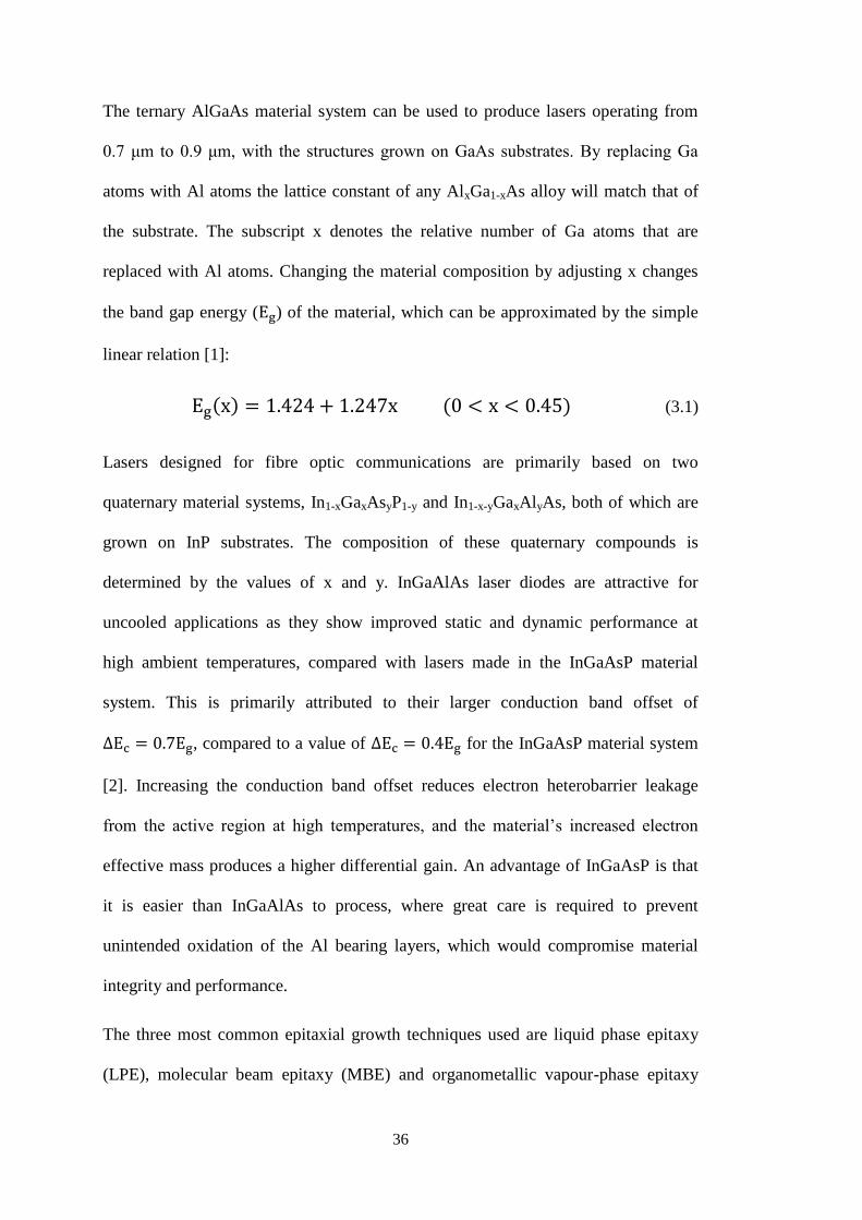
36
The ternary AlGaAs material system can be used to produce lasers operating from
0.7 μm to 0.9 μm, with the structures grown on GaAs substrates. By replacing Ga
atoms with Al atoms the lattice constant of any AlxGa1-xAs alloy will match that of
the substrate. The subscript x denotes the relative number of Ga atoms that are
replaced with Al atoms. Changing the material composition by adjusting x changes
the band gap energy ( ) of the material, which can be approximated by the simple
linear relation [1]:
( ) ( ) (3.1)
Lasers designed for fibre optic communications are primarily based on two
quaternary material systems, In1-xGaxAsyP1-y and In1-x-yGaxAlyAs, both of which are
grown on InP substrates. The composition of these quaternary compounds is
determined by the values of x and y. InGaAlAs laser diodes are attractive for
uncooled applications as they show improved static and dynamic performance at
high ambient temperatures, compared with lasers made in the InGaAsP material
system. This is primarily attributed to their larger conduction band offset of
, compared to a value of for the InGaAsP material system
[2]. Increasing the conduction band offset reduces electron heterobarrier leakage
from the active region at high temperatures, and the material’s increased electron
effective mass produces a higher differential gain. An advantage of InGaAsP is that
it is easier than InGaAlAs to process, where great care is required to prevent
unintended oxidation of the Al bearing layers, which would compromise material
integrity and performance.
The three most common epitaxial growth techniques used are liquid phase epitaxy
(LPE), molecular beam epitaxy (MBE) and organometallic vapour-phase epitaxy

37
(OMVPE). OMVPE is also referred to as metal-organic chemical vapour deposition
(MOCVD) [2]. Using a semiconductor substrate as a base material, layers with
different thickness and material composition are grown, one on top of the other, to
form the laser structure. Accurate control of the material composition and layer
thickness is required to ensure that the laser performs as designed.
3.1.1 Multi-quantum well structures
The first semiconductor lasers used a bulk active region, consisting of a layer of
intrinsic semiconductor material with a thickness in the region of 100 nm to 300 nm.
In such a structure the carriers are confined within a three dimensional potential well.
When the thickness of the heterostructure is reduced to the extent that it is
comparable to the de Broglie wavelength of the carrier, referring to the coordinates
shown in Fig. 3.1, the kinetic energy corresponding to the carrier motion along the y
direction is quantised. Since the electrons are still free to move in the x and z
directions this leads to a two dimensional quantisation of the density of states [3]. A
device with one thin active region such as this is called a single quantum well (SQW)
laser. Improved device performance can be achieved from a multi-quantum well
(MQW) structure [4], where multiple thin active layers are effectively stacked, one
on top of the other. The individual quantum wells are separated by thin barrier layers
of semiconductor material with a higher band gap than the quantum well layers. The
typical thickness of the quantum well and barrier layers is in the region of 5 to
20 nm. The energy band diagram for a MQW laser is illustrated in Fig. 3.2(a).
Fig. 3.2(b) illustrates the density of states for a MQW device where it has a step like
progression, also shown is the density of states for a bulk device which displays a
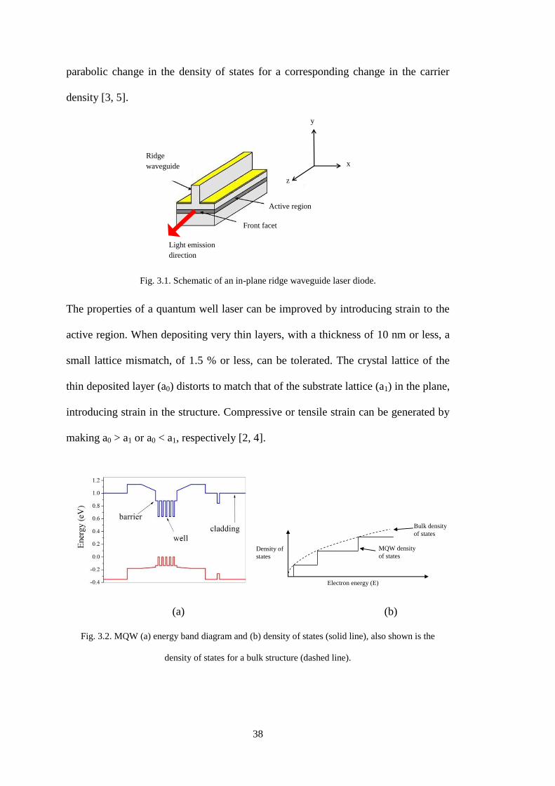
38
parabolic change in the density of states for a corresponding change in the carrier
density [3, 5].
Fig. 3.1. Schematic of an in-plane ridge waveguide laser diode.
The properties of a quantum well laser can be improved by introducing strain to the
active region. When depositing very thin layers, with a thickness of 10 nm or less, a
small lattice mismatch, of 1.5 % or less, can be tolerated. The crystal lattice of the
thin deposited layer (a0) distorts to match that of the substrate lattice (a1) in the plane,
introducing strain in the structure. Compressive or tensile strain can be generated by
making a0 > a1 or a0 < a1, respectively [2, 4].
(a) (b)
Fig. 3.2. MQW (a) energy band diagram and (b) density of states (solid line), also shown is the
density of states for a bulk structure (dashed line).
x
z
y
Ridge
waveguide
Active region
Front facet
Light emission
direction
Density of
states
Electron energy (E)
Bulk density
of states
MQW density
of states

39
3.2 Carrier and photon confinement
The most efficient type of laser is the electrically pumped semiconductor laser diode.
Overall power conversion efficiencies of ≈ 50 % are not uncommon, compared to
≈ 1 % for gas and solid state lasers. The higher efficiencies of diode lasers have also
been exploited by solid state lasers, where incoherent optical flash lamp sources are
replaced with diode laser pump sources [2]. An ideal laser diode generates a photon
for each injected carrier, with the photons being emitted in a controlled way so as to
maximise the amount of photons collected at the output. The efficiency of a real
device is determined by how well injected carriers and generated photons are
confined to the active region, and a number of structures have been developed which
achieve confinement in both the transverse and lateral directions.
3.2.1 Transverse confinement
Confinement is achieved in the transverse direction through the design of the
material layer structure. Modern semiconductor lasers are based on the double
heterostructure, where an intrinsic active region is sandwiched between highly doped
p and n cladding layers. The cladding layers have a higher conduction-valence band
energy gap ensuring that recombination of carriers can only take place in the active
region. The intrinsic active region, with its lower band gap, has a slightly higher
refractive index than the cladding layers and forms a dielectric waveguide in the
transverse direction [2]. In comparison to homojunctions, the double heterostructure
reduces the threshold currents necessary for lasing by a factor of ≈ 100, enabling the
development of modern semiconductor lasers [5, 6]. When quantum-well active
regions were first developed the thin dimensions of these structures produced weak
optical confinement. While MQWs did achieve higher confinement, the most
40
efficient solution was to add additional layers to act as passive waveguides forming a
structure called a separate confinement heterostructure (SCH) [4]. The SCH
effectively separates the design of the quantum well active region from the optical
confinement structure [6].
3.2.2 Lateral confinement
Confinement in the lateral direction is achieved by modifying the layers which were
uniformly deposited during the wafer growth. A structure with no lateral
confinement, apart from roughening the sides of the chip, is a broad-area structure.
Current is applied to the entire area of the substrate and light is emitted across the
width of the device. In modern applications such an inefficient structure is of limited
use, apart from quality control. Structures designed to achieve confinement in the
lateral direction have two main classifications, gain guided and index guided.
3.2.2.1 Gain guided structures
In a gain guided structure the optical mode is determined by the width of the optical
gain region. In contrast to a broad area device, current injection is limited to a
defined region of the junction, the dimensions of which determines the width of the
gain region. The simplest method used to achieve this is an oxide stripe structure,
where SiO2 oxide layers are formed at either side of the p contact layer. The SiO2
layers are insulating layers, therefore current only flows through the contact layer to
the active region under the p layer. Gain guided structures can also be fabricated
using a proton stripe structure where implanted ions (protons) create damage and trap
out mobile charge carriers, forming a highly resistive region at either side of the
p contact layer [2, 3]. Prior to the development of viable etching and regrowth
41
techniques, these structures were used [2]. In comparison to index guided structures,
discussed in the next section, gain guided structures are inefficient which limits their
suitability in most application areas. However, along with broad area devices, they
are useful in process control as the material quality can be characterised
independently of the processing steps.
3.2.2.2 Index guided structures
In an index guided structure the optical mode is formed by a region of higher
refractive index and the light is confined in a manner similar to an optical fibre.
Index guided structures can be described as weakly index guided or strongly index
guided [3]. The ridge waveguide structure combines current confinement with weak
index guiding of the optical mode. The ridge provides loading for index guiding,
while also acting as a narrow current confining strip [5, 3]. Optical lithography and
standard etching processes, such as inductive coupled plasma (ICP) dry etching, are
used to realise the ridge. The efficiency of the structure can be high, but because the
etching process used to form the ridge stops just above the active region, a portion of
the injected carriers can still diffuse laterally and recombine without contributing to
gain [2]. Fig. 3.3 (a) shows a facet view of a fabricated ridge waveguide taken using
a scanning electron microscope (SEM). Fig. 3.3 (b) shows a picture of the top surface
of a ridge waveguide laser chip. The ridge width is 2 μm in this device.
A buried heterostructure achieves strong confinement of carriers and photons. The
active region is completely surrounded by material with a wider bandgap and lower
refractive index; electromagnetically the active region forms a rectangular dielectric
waveguide. In comparison to the ridge waveguide structure, it is a more complex
structure, requiring a multistep growth process. Fig. 3.4 shows a cross section of one

42
type of structure called a semi-insulating buried heterostructure. In this example,
material is etched away from either side of the active region. The wafer is placed
back in the growth chamber and semi-insulating semiconductor material is regrown
to replace the material that was removed. There are a number of variations in the
structures that can be used to produce buried heterostructures but most employ a
regrowth step [2, 5].
(a) (b)
Fig. 3.3. Ridge waveguide (a) SEM image showing the front facet view and (b) a picture of the top-
surface of a fabricated laser diode chip.
Fig. 3.4. Buried hetrostructure with regrown semi-insulating semiconductor material.
3.3 Lasers for optical communications
Semiconductor laser diodes are the predominant optical source used in fibre optic
communications, providing transmitter sources as well as pump sources for optical
amplifiers. The devices used in the industry range from Fabry Pérot (FP) lasers to
more complex integrated tuneable modules. The first optical links used multimode
SI SI

43
FP lasers, however, the achievable bit-rate distance product was limited by
dispersion effects in optical fibre and mode partition noise in the laser [7, 8].
Increasing the bit-rate distance product provided the incentive to develop single
longitudinal mode lasers. This was particularly important in exploiting the lower loss
window at 1550 nm, as single mode operation was essential in minimising the effects
of higher dispersion in standard single mode fibre (SSMF) at this wavelength.
Optical communication applications employing single mode lasers specify a high
degree of spectral purity. The ratio of power in the single mode to the power in the
FP modes is a key figure of merit, characterised by the side mode suppression ratio
(SMSR), and for most applications a value greater than 30 dB is required. A number
of approaches have been developed to achieve single mode operation, but the basic
principle is to provide a filter mechanism, either internal in the laser cavity or
external, which delivers selective feedback to the laser cavity in order to select a
particular operating wavelength [2]. Fig. 3.5 shows typical optical spectra from (a) an
FP laser and (b) a single mode laser. A root-mean-square (rms) spectral width of 2 to
4 nm is typical for FP lasers, whereas values << 1 nm are required for single mode
lasers.
(a) (b)
Fig. 3.5. Optical spectrum from (a) an FP laser and (b) a single mode laser.

44
3.3.1 Fabry Pérot lasers
The simplest semiconductor laser diode structure is the FP laser, where a resonator is
formed by placing a gain medium between two mirrors. The mirrors in this case are
formed by the cleaved laser facets, which if left uncoated have a reflectivity of
≈ 30 %. The amount of light emitted from the front facet can be increased by placing
a high reflectivity (HR) coating on the back facet (>90 % typical) and a low
reflectivity (LR) coating on the front (10 to 30 % typical). In contrast to single mode
lasers, which will be discussed in subsequent sections, FP lasers have no frequency
selective elements and produce a multimode spectrum. The spectral modes are
equally spaced in frequency, ν, by ν , where is the speed of light, is the
group index of the waveguide and is the cavity length [9]. FP lasers are still an
important source in optical communications, particularly in short reach applications.
As FPs are mainly used in low cost applications, ridge waveguide devices are
preferred; also, the relative simplicity of the structure makes it cost effective to
produce, with high yields, theoretically 100 %. In the low dispersion window at
1310 nm, directly modulated lasers FP lasers can achieve relatively high bit rates
over short distances. In [8] it has been shown that by optimising the centre
wavelength, to take account of dispersion in single mode fibre, a transmission
distance of 7 km can be achieved in the 1310 nm window at 10 Gbit/s. At 1550 nm
the performance is limited by dispersion but they are still an important device for
lower speed short reach applications.
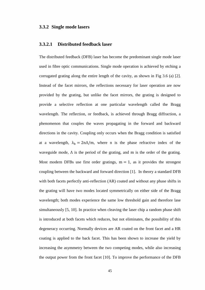
45
3.3.2 Single mode lasers
3.3.2.1 Distributed feedback laser
The distributed feedback (DFB) laser has become the predominant single mode laser
used in fibre optic communications. Single mode operation is achieved by etching a
corrugated grating along the entire length of the cavity, as shown in Fig 3.6 (a) [2].
Instead of the facet mirrors, the reflections necessary for laser operation are now
provided by the grating, but unlike the facet mirrors, the grating is designed to
provide a selective reflection at one particular wavelength called the Bragg
wavelength. The reflection, or feedback, is achieved through Bragg diffraction, a
phenomenon that couples the waves propagating in the forward and backward
directions in the cavity. Coupling only occurs when the Bragg condition is satisfied
at a wavelength, , where n is the phase refractive index of the
waveguide mode, is the period of the grating, and is the order of the grating.
Most modern DFBs use first order gratings, , as it provides the strongest
coupling between the backward and forward direction [1]. In theory a standard DFB
with both facets perfectly anti-reflection (AR) coated and without any phase shifts in
the grating will have two modes located symmetrically on either side of the Bragg
wavelength; both modes experience the same low threshold gain and therefore lase
simultaneously [5, 10]. In practice when cleaving the laser chip a random phase shift
is introduced at both facets which reduces, but not eliminates, the possibility of this
degeneracy occurring. Normally devices are AR coated on the front facet and a HR
coating is applied to the back facet. This has been shown to increase the yield by
increasing the asymmetry between the two competing modes, while also increasing
the output power from the front facet [10]. To improve the performance of the DFB
46
it is desirable to leave a fraction of a wavelength shift near the centre of the cavity, as
shown in Fig. 3.6 (b), where the grating is shifted by . This produces a phase
shift of and facilitates lasing at the Bragg wavelength [2, 1]. These are called
quarter wave shifted DFBs.
In comparison to an FP wafer, the fabrication of a DFB wafer is more complex
requiring additional steps. The grating is formed by transferring the grating pattern to
a resist using a high precision lithography technique, such as Ebeam. The patterned
resist acts as a mask for a chemical etching process used to form the grating. After
formation of the grating, the wafer is placed back in the growth chamber and
additional layers are deposited in a second regrowth step [1].
Fig. 3.6. Schematic for (a) standard DFB and (b) quarter wave shifted DFB.
3.3.2.2 Distributed Bragg reflector laser
In a distributed Bragg reflector (DBR) laser one, or both, of the facet mirrors is
replaced with a passive grating reflector. In comparison to a DFB, where the grating
is embossed on the active material over the entire cavity length, the grating in a DBR
is formed in a passive section at one, or both, ends of the laser, as shown in
Fig. 3.7 [1]. The processing required to fabricate a DBR is quite complex. Active and

47
passive sections are grown in a multistep growth process, and very accurate control
of the layer thickness is required to ensure coherence along the axial direction.
Because the DBR process is more complex than the DFB manufacturing process,
DBRs are not normally used as single frequency devices, but instead utilised when
their unique properties are required [2]. Multi-section devices have been fabricated
where the gain, phase and Bragg frequency can be independently controlled via
separate bond pads in order to tune the wavelength. Widely tuneable lasers covering
the entire C or L-band have been commercialised based on multi section DBRs
called sampled grating DBRs (SGDBR). Instead of periodic gratings, a periodic
modulation is introduced enabling tuning over a wide wavelength range.
Fig. 3.7. Schematic of a DBR laser.
3.3.2.3 Vertical cavity surface emitting laser
The emission direction in a vertical cavity surface emitting laser (VCSEL) is
perpendicular to the wafer surface, making it possible to achieve very short cavities,
as the cavity length is dependent on the layer thickness and not the cleaved cavity
length. The device is grown in a stack like process and the structure is illustrated in
Fig. 3.8, where a cross section shows the active region sandwiched between two high
reflectivity DBR mirrors [1]. As the gain region is very short, mirrors with high
mean reflectivity, typically > 99 %, are required, in order to produce an efficient
device [2]. The DBR mirrors produce a relatively wide mirror loss minimum,
compared to that achieved in an in-plane DBR laser. This is offset by the VCSELs

48
short cavity, which increases the mode spacing so that adjacent modes experience a
higher mirror loss. When the gain curve of the laser is taken into consideration, the
roll-off in gain experienced by the adjacent modes is more important than the roll-up
in the mirror loss in achieving single mode operation [2]. Current confinement can be
achieved by ion implantation, where ions are implanted to a selected area making it
non-conducting. The top of the device is metallised for contacting but a circular
aperture is created for light emission. The device produces an emitted beam with a
circular far field, which is beneficial when coupling light to an optical fibre. An
advantage of VCSELs, over edge emitters, is that the surface emitting geometry
facilitates wafer level testing of the devices. A high level of precision is needed in
the growth of a VCSEL wafer, as the single mode wavelength has a high dependence
on the thickness of the structure’s epitaxial layers. Specifically, a 1% change in
thickness of the structure’s epitaxial layers will result in a 10 nm shift in the cavity
resonance [11] with consequent variation in the lasing wavelength, threshold gain
and threshold current. The VCSEL’s short cavity length places significant demands
on the high mirror reflectivity required to allow lasing. For short wavelengths the
AlGaAs material system can provide high reflectivity (>0.999) from two dozen
periods. Unfortunately, lattice matched semiconductor materials in the InP material
system have low absorption at long wavelengths and provide insufficient index
contrast. This makes the realisation of highly reflective mirrors difficult, requiring an
impractically large number of mirror pairs. Therefore, in this system usually one, or
both, of the mirrors is formed by non-epitaxial growth [2, 12], which is undesirable
as it adds an additional high complexity step to the fabrication process.
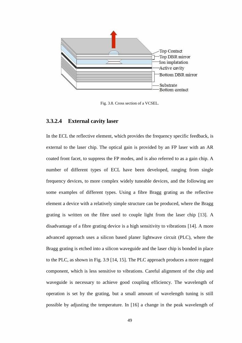
49
Fig. 3.8. Cross section of a VCSEL.
3.3.2.4 External cavity laser
In the ECL the reflective element, which provides the frequency specific feedback, is
external to the laser chip. The optical gain is provided by an FP laser with an AR
coated front facet, to suppress the FP modes, and is also referred to as a gain chip. A
number of different types of ECL have been developed, ranging from single
frequency devices, to more complex widely tuneable devices, and the following are
some examples of different types. Using a fibre Bragg grating as the reflective
element a device with a relatively simple structure can be produced, where the Bragg
grating is written on the fibre used to couple light from the laser chip [13]. A
disadvantage of a fibre grating device is a high sensitivity to vibrations [14]. A more
advanced approach uses a silicon based planer lightwave circuit (PLC), where the
Bragg grating is etched into a silicon waveguide and the laser chip is bonded in place
to the PLC, as shown in Fig. 3.9 [14, 15]. The PLC approach produces a more rugged
component, which is less sensitive to vibrations. Careful alignment of the chip and
waveguide is necessary to achieve good coupling efficiency. The wavelength of
operation is set by the grating, but a small amount of wavelength tuning is still
possible by adjusting the temperature. In [16] a change in the peak wavelength of

50
0.014 nm / ˚C was reported for a PLC based device; however, mode hopping was
observed in this device over a temperature range 16 to 42 ˚C.
Fig. 3.9. Schematic of an ECL based on a PLC platform [14].
Tuneable ECLs can be realised using diffraction gratings to select different
longitudinal mode numbers by controlling the angle of the grating, or the angle at
which light hits the grating, to provide selective feedback to the laser. Two
commonly used configurations are Littrow and Littman. In the Littrow configuration
the operating wavelength is selected by rotating the grating, as shown in
Fig. 3.10 (a). In the Littman configuration, shown in Fig. 3.10 (b), the light from the
grating hits a reflective element, either a mirror or a prism, and the feedback to the
laser is controlled by the angular position of the reflective element. As the grating is
fixed, the position of the output beam remains constant. Littrow and Littman ECLs
have different characteristics making them suitable for different types of
applications. The Littrow ECL is easy to align, cost effective and has a larger output
power than Littman ECL. The main drawback is that the position of the beam moves
when tuning the wavelength. If wavelength tuning of more than a few GHz is
required and the positional stability of the beam is a requirement, as is the case when
coupling to an optical fibre, the Littman resonator is preferable [17].

51
Fig. 3.10. ECL in (a) Littrow configuration and (b) Littman configuration [17].
A second, more compact, ECL structure uses two thermally tuneable silicon etalon
filters to select the operating wavelength [18, 19]. A simplified diagram of the
structure is shown in Fig. 3.11. The silicon etalon filters form a pair of FP filters with
slightly differing periods. Tuneability is achieved using the Vernier effect, and full C
or L-band coverage can be achieved. To select a particular wavelength the
temperature of the first etalon is adjusted to place a transmission peak at the target
wavelength. The temperature of the second etalon is also adjusted to place a peak in
its transmission curve at the same target wavelength. Because of the slightly differing
periods of the two etalons the target wavelength is the only wavelength at which two
transmission peaks coincide, and the transmission is a maximum at this point. Light
at the target wavelength passes through the filter and is reflected by the mirror back
to the laser chip [20]. Precise independent temperature control of the two silicon
filters is necessary to suppress mode hopping. Such a device can achieve linewidths
below 100 kHz, however the increased complexity increases the packaging cost,
compared to monolithic lasers or fixed frequency ECLs.
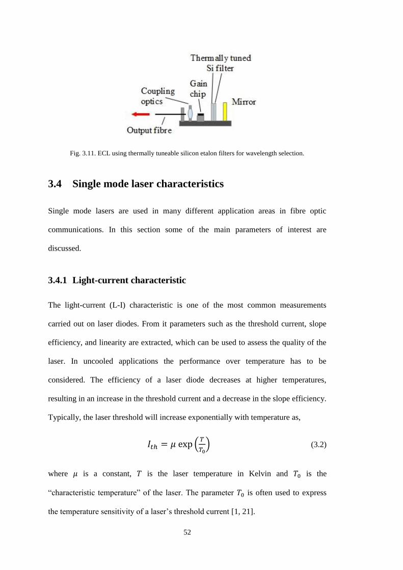
52
Fig. 3.11. ECL using thermally tuneable silicon etalon filters for wavelength selection.
3.4 Single mode laser characteristics
Single mode lasers are used in many different application areas in fibre optic
communications. In this section some of the main parameters of interest are
discussed.
3.4.1 Light-current characteristic
The light-current (L-I) characteristic is one of the most common measurements
carried out on laser diodes. From it parameters such as the threshold current, slope
efficiency, and linearity are extracted, which can be used to assess the quality of the
laser. In uncooled applications the performance over temperature has to be
considered. The efficiency of a laser diode decreases at higher temperatures,
resulting in an increase in the threshold current and a decrease in the slope efficiency.
Typically, the laser threshold will increase exponentially with temperature as,
(
) (3.2)
where is a constant, is the laser temperature in Kelvin and is the
“characteristic temperature” of the laser. The parameter is often used to express
the temperature sensitivity of a laser’s threshold current [1, 21].

53
When a laser chip is packaged, the chip to fibre coupling efficiency achieved is a key
parameter, as together with the slope efficiency from the chip it determines the
overall slope efficiency of the module. The coupling efficiency can be easily
determined by comparing the L-I’s from the module and the chip prior to packaging.
A laser package usually incorporates a monitor photodiode, which collects the light
from the laser’s back facet. The signal from the photodiode can be applied to a
feedback circuit in the laser driver in order to control the output power from the
module. In uncooled applications this is used to keep the optical power constant over
the operating temperature range. Changes in the coupling efficiency can result in
inaccuracies between the monitor photodiode current and the expected output power
from the module. Variations which occur over temperature can be characterised by
measuring a modules L-I at different temperatures, from which, an extracted
parameter called the tracking error can be used to quantify the error. Causes of
tracking error include instabilities in the output beam from the laser chip, such as a
shift in the far field with temperature, or bias current, and changes in the mechanical
alignment of the light coupling optics.
3.4.2 Side mode suppression ratio
Single mode lasers need to maintain a high SMSR under all operating conditions,
which may include modulation of the bias current and operation over a specified
temperature range. For most applications a minimum SMSR of 30 dB is required and
this can be met by modern devices which can deliver typical values greater than
40 dB. For most applications continuous tuning, i.e. no mode hops, over the
operating temperature and bias current ranges is required.

54
3.4.3 Relative intensity noise
When a laser is operated CW the carrier and photon densities are not constant,
instead random carrier and photon recombination and generation events produce
instantaneous time variations in the carrier and photon densities [2]. These random
variations lead to variations in the magnitude of the output power from the laser,
creating a noise source that is referred to as the relative intensity noise (RIN), defined
by:
( )
( ) (3.3)
where ( ) is the mean square intensity-fluctuation spectral-density of an optical
signal and is the average optical power. RIN can limit the performance of
optical systems; therefore, low RIN is desirable for these systems.
3.4.4 Modulation bandwidth
The modulation bandwidth determines the maximum data rate that can be transmitted
by a directly modulated laser. Fig. 3.12 shows the amplitude versus frequency
response, or S21, for a typical single mode laser measured using a vector network
analyser (VNA). The maximum achievable data rate can be estimated from the 3 dB
bandwidth point, F3dB, shown in the figure. It can be assumed that the minimum
bandwidth required for a digital link is 75 % of the link bit rate; however, in order to
optimise performance and yield most lasers are designed to exceed this minimum. At
a chip level the relaxation oscillation frequency, , limits the achievable bandwidth.
It can be measured using a VNA, as shown in Fig. 3.12, or from the RIN spectrum.
Using the RIN spectrum allows the intrinsic frequency response of the laser to be
determined without the influence of electrical parasitics. is given by,

55
√
(3.4)
where is the group velocity, is the differential gain, is the average photon
density inside the active layer, and is the photon lifetime in the cavity [6]. As
evident from (3.4) increasing the photon density, by increasing the output power
from the laser, is one approach to increase ; however, increased damping of the
resonance at high powers, thermal limitations and high power facet damage set
practical limitations on the output power that can be used [2]. A further consideration
is that the drive current and output power levels need to meet the specification of the
target application. As discussed previously, MQW lasers have a higher differential
gain and provide a platform for designing high speed lasers at relatively low drive
currents (< 100 mA) [6].
In a packaged device the electrical performance of both the chip and the packaging
platform has to be optimised. Electrical parasitics can limit the high speed
performance and steps such as minimising the size of the bond pad and using a deep
ridge etch or current blocking layers in the longitudinal direction, parallel to the laser
cavity can be employed to reduce the capacitance of the laser chip. When packaging
high speed laser chips the packaging platform is carefully designed to optimise its
high speed performance. This involves choosing materials, such as TO-can headers
or high speed butterfly packages, that are designed for high speed operation. At
2.5 Gbit/s the connections within the package can be made with wire bonds, but at
higher speeds of 10 Gbit/s and above the length of the wire bonds need to be
minimised, in order to reduce parasitic inductance [22]. An alternative to wire bonds
is to use transmission lines on specially designed submounts to distribute the high
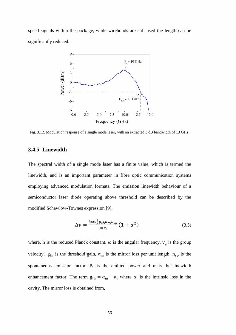
56
speed signals within the package, while wirebonds are still used the length can be
significantly reduced.
Fig. 3.12. Modulation response of a single mode laser, with an extracted 3 dB bandwidth of 13 GHz.
3.4.5 Linewidth
The spectral width of a single mode laser has a finite value, which is termed the
linewidth, and is an important parameter in fibre optic communication systems
employing advanced modulation formats. The emission linewidth behaviour of a
semiconductor laser diode operating above threshold can be described by the
modified Schawlow-Townes expression [9],
( ) (3.5)
where, is the reduced Planck constant, is the angular frequency, is the group
velocity, is the threshold gain, is the mirror loss per unit length, is the
spontaneous emission factor, is the emitted power and is the linewidth
enhancement factor. The term where is the intrinsic loss in the
cavity. The mirror loss is obtained from,

57
(
) (3.6)
where L is the cavity length, R1 and R2 are the front and back facet reflectivities,
respectively. From these expressions it is evident that the linewidth can be reduced
by (i) increasing the output power, (ii) reducing the laser linewidth enhancement
factor and (iii) reducing the mirror loss. Therefore, it is desirable to operate the laser
at high bias currents in order to achieve higher output powers. Also, high output
power can be achieved through design of the laser and epitaxial structure. However,
other design parameters, such as the maximum bias current allowable for the
application, have to be taken into account. The α factor is largely dependent on the
material properties. Quantum well structures have a lower α factor compared to bulk
structures [1], and it can be decreased by adding strain to the quantum well active
region and can be further decreased by adding p-doping in the strained active region
[23]. The α factor is also dependent on the wavelength, and the value varies across
the laser’s gain curve with lower values being observed at shorter wavelengths [7].
Therefore, detuning the peak wavelength to the shorter side of the gain peak will
reduce the linewidth. As evident from (3.6), can be reduced by increasing the
cavity length and, or, increasing the facet reflectivity. Using (3.5) and typical
parameters for a monolithic single mode laser listed in table 3.1, the linewidth was
simulated for three variables: (i) inverse power in the laser cavity, (ii) cavity length
and (iii) front facet reflectivity, the results of which are plotted in Fig. 3.13, Fig. 3.14
and Fig. 3.15, respectively.
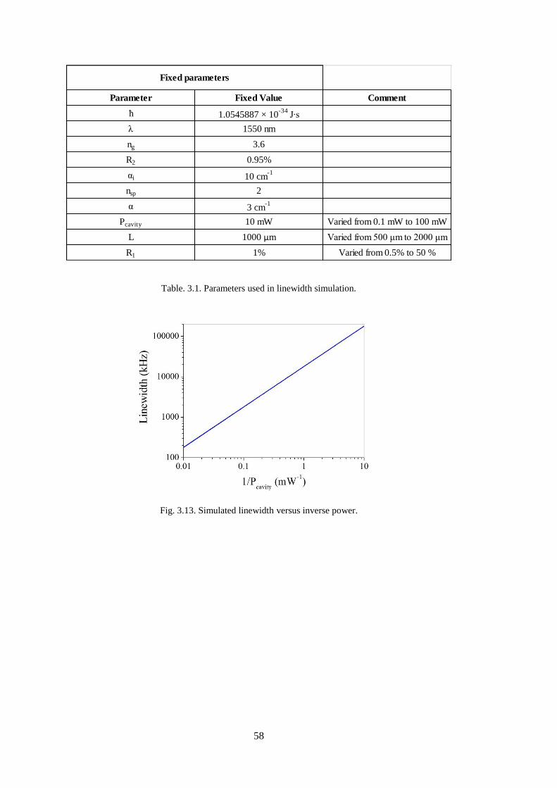
58
Table. 3.1. Parameters used in linewidth simulation.
Fig. 3.13. Simulated linewidth versus inverse power.
Parameter Fixed Value Comment
ħ 1.0545887 × 10⁻³⁴
J∙s
λ 1550 nm
ng 3.6
R2 0.95%
αi 10 cm-1
nsp 2
α 3 cm-1
Pcavity 10 mW Varied from 0.1 mW to 100 mW
L 1000 μm Varied from 500 μm to 2000 μm
R1 1% Varied from 0.5% to 50 %
Fixed parameters

59
Fig. 3.14. Simulated linewidth versus cavity length.
Fig. 3.15. Simulated linewidth versus front facet reflectivity.
The approach of reducing the linewidth by increasing the cavity length has been
applied to DFB lasers. In [23] a linewidth of 70 kHz was demonstrated using a cavity
length of 1450 μm. The device used uncoated facets, and as shown in Fig. 3.15 the
linewidth can be reduced substantially by increasing the front facet reflectivity.
However, it was reported that secondary modes began to appear at higher output
powers. To suppress this behaviour, and improve overall performance and yield,
DFBs are normally AR coated on the front facet and HR coated on the back [10].
However, the AR coating will increase the linewidth.
60
3.5 Conclusion
This chapter reviewed the basic structures of semiconductor lasers. Lasers used in
optical communications were reviewed and approaches used to achieve single mode
operation were discussed. Also, characteristics of interest for optical communications
were considered. In the next chapter we describe a novel approach to producing
single mode lasers.
References
[1] G. P. Agrawal, Lightwave Technology : components and devices, Hoboken: Wiley,
2004.
[2] L. A. Coldren, Diode Lasers and Photonic Integrated Circuits, Hoboken: Wiley, 2012.
[3] G. P. Agrawal and N. K. Dutta, Long wavelength Semiconductor Lasers, New York:
Von Nostrand Reinhold, 1986.
[4] P. S. Zory, Quantum Well Lasers, San diego: Academic Press, 1993.
[5] J. M. Senior, Optical Fiber Communications: Principles and Practice, 3rd ed., New
York: Prentice Hall, 2009.
[6] W. F. Brinkman, T. L. Koch, D. V. Lang and D. P. Wilt, “The lasers behind the
communications revolution,” Bell Labs Technical Journal, vol. 5, no. 1, pp. 150-167,
2002.
[7] K. Petermann, Laser Diode Modulation and Noise, London: Kluwer Academic, 1991.
[8] K. Nakahara, T. Tsuchiya, E. Nomoto and M. Mukaikubo, “Transmission Properties
of 1.3-μm InGaAlAs MQW FP Lasers in 10-Gb/s Uncooled Operation,” Journal of
Lightwave Technology, vol. 23, no. 12, pp. 3997-4003, Dec. 2005.
[9] J. Buus, Single Frequency Semiconductor Lasers, Bellingham: SPIE Optical
Engineering Press, 1990.
[10] T. Kjellberg, S. Nilsson, T. Klinga, B. Broberg and R. Schatz, “Investigation on the
spectral characteristics of DFB lasers with different grating configurations made by
electron-beam lithography,” Journal of Lightwave Technology, vol. 11, no. 9, pp.
1405-1415, Sep. 1993.
61
[11] C. Chang-Hasnain, “Tunable VCSEL,” IEEE Journal of Selected Topics in Quantum
Electronics, vol. 6, no. 6, pp. 978-987 , Nov. 2000.
[12] M. Muller, W. Hofmann, G. Bohm and M. C. Amann, “Short-Cavity Long-
Wavelength VCSELs With Modulation Bandwidths in Excess of 15 GHz,” IEEE,
Photonics Technology Letters, vol. 21, no. 21, pp. 1615-1617, Aug. 2009.
[13] D. M. Bird, J. R. Armitage, R. Kashyap, R. M. A. Fatah and K. H. Cameron, “Narrow
line semiconductor laser using fibre grating,” Electronic letters, vol. 27, no. 13, pp.
1115-1116, Jun. 1991.
[14] M. Alalusi, P. Brasil, S. Lee, P. Mols and L. Stolpner, “Low noise planar external
cavity laser for interferometric fiber optic sensors,” in Volume 7316 of Proceedings of
Spie, Fiber Optic Sensors and Applications VI, 2009.
[15] J. Tidmarsh, S. Fasham, P. Stopford, A. Tomlinson and T. Bestwick, “A narrow
linewidth laser for WDM applications using silicon waveguide technology,” in IEEE
Lasers and Electro-Optics Society (LEOS) 12th Annual Meeting , San Francisco, Nov.
1999.
[16] K. Numata, J. Camp, M. A. Krainak and L. Stolpner, “Performance of planar-
waveguide external cavity laser for precision measurements,” Optics Express, vol. 18,
no. 22, pp. 22781-22788, Oct. 2010.
[17] C. Ye, Tunable External Cavity Diode Lasers, Singapore: World Scientific Publishing
Co. Pte. Ltd., 2004.
[18] M. McDonald, A. Daiber, M. Finot and S. Xu, “Wavelength Filter with Integrated
Thermal Control used as an Intracavity DWDM Laser Tuning Element,” in
IEEE/LEOS International Conference on Optical MEMS and Their Applications
Conference, Big Sky, Aug. 2006.
[19] A. Daiber, C. Schulz, J. C. Lo, P. Ludwig and S. Xu, “Tunable DWDM XFP with an
external cavity laser transmitter and transmission performance matching 300-pin
transponders,” in Optical Fiber Communication Conference (OFC), Los Angeles, Mar.
2010.
[20] M. Finot, M. McDonald, A. Daiber, W. B. Chapman, D. Li, M. Epitaux, E. Zbinden, J.
Bennett, W. J. Kozlovsky and J. M. Verdiel, “Automated Optical Packaging
Technology for 10 Gb/s Transceivers and its Application to a Low-Cost Full C-Band
Tunable Transmitter,” Intel Technology Journal, vol. 8, no. 2, pp. 101-114, May 2004.

62
[21] T. Hertsens, “ILX lightwave, Application note #5, An Overview of Laser Diode
Characteristics,” 2005. [Online]. Available:
http://www.ilxlightwave.com/appnotes/AN%205%20REV02%20LD%20Characteristi
cs%20Overview.pdf.
[22] W. Han, M. Rensing, X. Wang, H. Yang, F. H. Peters and P. O'Brien, “Investigation of
the Packaging-Induced RF Attenuations and Resonances in a Broadband
Optoelectronic Modulator Module,” Journal of Lightwave Technology, vol. 30, no. 16,
pp. 2610-2617, Aug. 2012.
[23] H. Bissessur, C. Starck, J. Y. Emery, F. Pommereau, C. Duchemin, J. G. Provost, J. L.
Beylat and B. Fernier, “Very narrow-linewidth (70 kHz) 1.55 um strained MQW DFB
lasers,” Electronics Letters, vol. 28, no. 11, pp. 998-999, May 1992.
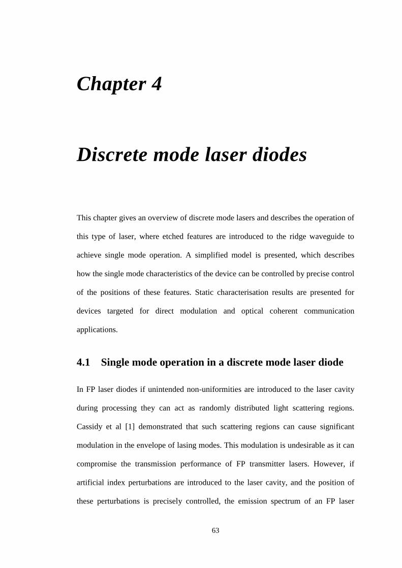
63
Chapter 4
Discrete mode laser diodes
This chapter gives an overview of discrete mode lasers and describes the operation of
this type of laser, where etched features are introduced to the ridge waveguide to
achieve single mode operation. A simplified model is presented, which describes
how the single mode characteristics of the device can be controlled by precise control
of the positions of these features. Static characterisation results are presented for
devices targeted for direct modulation and optical coherent communication
applications.
4.1 Single mode operation in a discrete mode laser diode
In FP laser diodes if unintended non-uniformities are introduced to the laser cavity
during processing they can act as randomly distributed light scattering regions.
Cassidy et al [1] demonstrated that such scattering regions can cause significant
modulation in the envelope of lasing modes. This modulation is undesirable as it can
compromise the transmission performance of FP transmitter lasers. However, if
artificial index perturbations are introduced to the laser cavity, and the position of
these perturbations is precisely controlled, the emission spectrum of an FP laser

64
diode can be altered in a controlled way. Index perturbations have been introduced to
laser cavities using a variety of methods, with the first demonstration using a laser
cutting tool to etch slots in the laser cavity [2, 3]. Significant modulation of the
optical spectra was observed using this approach and even single mode behaviour,
with an SMSR > 20 dB, was demonstrated. However, the single mode behaviour was
accompanied by large increases in threshold currents and much reduced slope
efficiencies as a result of loss introduced by the slots created using this method. Later
work demonstrated that slots could be etched using focused ion beam etching (FIBE)
[4] and reactive ion etching [5]. In terms of developing a process that could be
applied to volume manufacture of semiconductor lasers, the latter method was the
most practical. While the initial devices produced using these approaches
demonstrated single longitudinal mode operation they did so under a limited range of
operating conditions, displaying mode hops with variation in the bias current and
temperature [6]. The laser devices used in this work build on this early work,
particularly that of [5], and are referred to as discrete mode laser diodes.
4.1.1 Theory of operation
Single wavelength operation in DMLDs is achieved by introducing index
perturbations in the form of shallow-etched features, or slots, positioned at a small
number of sites distributed along the ridge waveguide. The slots are realized using
ICP dry etching, with a typical depth in the region of 1.5 μm to 2 μm and a width of
approximately 1 μm. Fig. 4.1(a) shows a SEM image where slots are etched into the
ridge using this process. The slots are relatively shallow and are not etched into the
active (wave guiding) region, however, they will still interact with the modes electric
field (and magnetic field) as the mode profile is not fully confined to the active

65
region and will expand into the surrounding cladding regions. This interaction results
in a proportion of the propagating light being reflected at the boundaries between the
perturbed and the unperturbed sections. In effect the slots act as reflection centres
and through suitable positioning the slots manipulate the mirror loss spectrum of an
FP laser so that the mirror loss of a specified mode is reduced below that of the other
cavity modes [7]. Using a simplified model, developed in [8, 9], a slot can be
described as a one dimensional discontinuity inserted into the cavity; as most of the
reflection comes from the front of the slot interface, the slot width has minimal effect
on the reflection and is not considered in the model. Fig. 4.1(b) shows a schematic of
a laser cavity with slots introduced into the cavity; where rs is the slot reflectivity, ts
is the slot transmission, N is the number of slots, L is the distance between the slots,
and ϒi is the reflectivity in a section of the cavity where i is the slot number. The
reflectivity from the first slot, ϒ1 is given by rs.
The introduction of a slot into the waveguide changes its effective refractive index,
so that it differs slightly from the segments of the waveguide without slots. The
reflectivity from the waveguide to slot interface can be approximated using:
(
) (4.1)
where n1 is the effective refractive index of the waveguide and n2 is the effective
refractive index of the waveguide with a slot.

66
(a) (b)
Fig. 4.1. (a) SEM image of 2μm wide ridge waveguide with etched slots. The slot width is 1 μm and
the spacing between the slots is 4 μm in this example. (b) Illustration of slot reflection and
transmission for N slots.
Assuming no loss from the slot,
(4.2)
ϒ2 is the reflectivity from the second slot and is given by
(4.3)
where β is the complex propagation constant, and the term ts is squared to take
account of forward and backward travelling waves. The exponential term describes
the medium in which the light travels, and a factor of 2 is used again to take account
of forward and backward travelling waves. The complex propagation constant takes
account of the gain and loss in the transmission medium and is defined in terms of
(4.4)
where n is the refractive index, λ is the wavelength, is the optical gain and αi is the
internal cavity loss.
1m
67
The reflectivities from the third and fourth slots are given by:
(4.5)
and,
(4.6)
respectively. Therefore, the reflectivity obtained from four slots is given by:
ϒtotal = ϒ1 + ϒ2 + ϒ3 + ϒ4
= rs + rsts2exp(-2iβL) + rsts
4exp(-4iβL) + rsts
6exp(-6iβL) (4.7)
By letting
(4.8)
the total reflectivity from N slots can be expressed by the following series
ϒtotal = rs( 1 + X + X2 + X3 + . . . . . . + XN-1) (4.9)
Which in terms of known variables can be described as
ϒ [ (
)
] (4.10)
The power reflection is related to the reflection amplitude by,
ϒ (4.11)
68
Using this model the power reflection versus wavelength was simulated for different
slot patterns in the 1550 nm window. The refractive indices were set to
n1 = n = 3.1838 and n2 = 3.1808. The following simplifications were used in the
model: changes in the refractive index due to changes in the carrier density were not
taken in to account, the loss introduced by the slots and the internal cavity loss were
set to zero, and the gain was set to 1 and showed no dependence on wavelength.
With N = 30, Fig. 4.2 plots the overlapped results of a simulation where the slot
spacing is varied from 3.31 μm to 3.46 μm in increments of 0.03 μm. Using a fixed
slot spacing of 3.4 μm, Fig. 4.3 plots the overlapped results of a simulation where N
equals 10, 20, 25 and 30. The overlapped results show that the power reflection
increases as the number of slots introduced into the cavity is increased. While it is
desirable to have the power reflection as large as possible, there are practical
limitations for a real device that limit the number of slots that are introduced into the
cavity, such as the cavity length. Also, the slots introduce loss and therefore to
optimise the efficiency of the device only the requisite number required to achieve a
given performance level should be introduced into the cavity.
Fig. 4.2. Overlapped power reflection versus wavelength simulation results, for slot spacing ranging
from 3.31 μm to 3.46 μm.

69
Fig. 4.3. Overlapped power reflection versus wavelength simulation results, for slot numbers ranging
from 10 to 30.
In semiconductor lasers once threshold is reached the carrier density clamps at that
value and any increase in injected carriers does not lead to an increase in carrier
density but rather the generation of photons through stimulated emission [10].
Another effect of increasing the level of injected carriers is the generation of heat
within the active region as a result of Joule heating [11]. The amount of heat
generated depends on a number of factors including the laser resistance, cavity
length, chip thickness, metal thickness on the chip and the quality of the eutectic
bonding of the chip to the submount. The refractive index of the semiconductor
material is dependent on its temperature, so any changes in temperature due to Joule
heating, or in the ambient temperature, will change the refractive index resulting in a
corresponding change in the peak reflection wavelength. The change in peak
wavelength versus temperature for single mode semiconductor lasers is typically
0.1 nm/°C [12]. As stated previously the heat generated as a result of injected current
depends on the laser design and packaging, and a typical value for a 1 mm cavity
device would be 4 pm/mA. Fig. 4.4 plots the peak reflection wavelength versus
refractive index for a slot spacing of 3.4 μm and N = 30. The refractive indices of the

70
waveguide with and without slots will change at the same rate versus temperature
and in the simulation n2 = n1 - 0.003.
Fig. 4.4. Simulated reflection peak wavelength versus refractive index.
The main focus of this chapter is DMLDs designed for fibre optic communication
applications. However, the DMLD process can be used with other material systems
to produce single mode lasers operating from the visible [13] to the mid-infrared
[14, 15] regions of the optical spectrum. Single mode lasers are important
components for use in other application areas such as gas sensing, atomic clocks and
LIDAR. Fig. 4.5 shows examples of optical spectra measured from DMLDs designed
for non-telecom applications. The devices have peak wavelengths of (a) 684 nm
(AlGaInP/GaAs), (b) 779 nm (AlGaAs/GaAs), (c) 1276 nm (InGaAlAs/InP), (d)
1393 nm (InGaAlAs/InP), (e) 1645 nm (InGaAlAs/InP), and (f) 2002 nm
(InGaAs/InP).

71
(a) (b)
(c) (d)
(e) (f)
Fig. 4.5. Spectra measured for DMLDs with operating wavelengths of (a) 684 nm, (b) 779 nm, (c)
1276 nm, (d) 1393 nm, (e) 1645 nm, and (f) 2002 nm.
In [15] a DMLD was fabricated using InGaAs/AlAsSb on InP quantum cascade
epitaxial materials and demonstrated single mode laser emission at λ ≈ 3.3 μm.
Fig. 4.6 shows the measured spectrum with emission wavelength of 3.3 μm and a
minimum SMSR of 25 dB, the value of which was limited by the noise floor of the

72
Fourier transform infrared (FTIR) spectrometer. For comparison the emission
spectrum of an FP laser fabricated on the same wafer is also shown.
Fig. 4.6. Single mode wavelength emission spectrum of a DMLD fabricated on InGaAs/AlAsSb
quantum cascade materials showing an SMSR of 25dB, also overlapped is the broad emission
spectrum from an FP laser from the same wafer.
4.2 Characterisation of DMLDs for fibre optic
communications
Lasers used in fibre optic communications are designed to meet target specifications
determined by the specific application. Access and enterprise markets require
directly modulated lasers capable of operating without a thermoelectric cooler
(TEC), while still operating in a predictable fashion over the specified temperature
range [16]. Similar to the electronics industry, fibre optic components are also graded
by operating temperature with temperature (T) ranges of -0 ˚C ≤ T ≤ 70 ˚C specified
for the standard or commercial grade and -40 ˚C ≤ T ≤ 85 ˚C specified for industrial
grade devices [17]. Single mode lasers designed for these applications are required to
maintain single mode operation over the temperature range while still maintaining

73
high output powers in excess of 5 mW from the chip, even at the upper temperature
in the range. In applications where precise wavelength control is required a TEC is
incorporated into the package to maintain the temperature of the laser chip at a set
point. Because temperature control is employed, the operating temperature range of
the laser chip can be relaxed. However, other parameters can be important for these
applications, such as the linewidth in coherent communications for example.
The DMLDs described in the rest of this chapter used an AlGaInAs MQW epitaxial
structure. The structure was grown on an n-type (100)-InP substrate in an OMVPE
reactor at low pressure. The MQW active region was sandwiched between two
InGaAsP SCH guide layers, which also acted as an etch stop layer for the ridge
waveguide. A p-InP layer was grown on top of the SCH followed by a highly
p-doped InGaAs contact layer. Electrical contacting was achieved using conventional
metals (Ti/Pt/Au) and SiO2 as an insulator for contact definition on the cap layer.
Finally the wafers were thinned by mechanical polishing, n-metal (Ti/Pt/Au)
deposited, the devices cleaved into the designed cavity length and the front and back
facets coated.
4.2.1 Directly modulated lasers
DMLDs for uncooled directly modulated applications were designed at both
1310 nm and 1550 nm. Static characterisation of the devices was performed and the
results are presented here.
74
4.2.1.1 1310 nm window
The structure of a 1310 nm DMLD designed for direct modulation at 2.5 Gbit/s is as
follows. The undoped laser active region consists of five compressively strained
AlGaInAs quantum wells with a well thickness of 5 nm whose composition is chosen
to give an emission wavelength centred at λ = 1.3 μm. The ridge width is
approximately 2.5 μm and the slots in the ridge had a width of around 1 μm. A
pattern of index perturbations was calculated to give single mode emission at
λ = 1295 nm at 25 ˚C. The slot pattern featured 20 index perturbations distributed
along the laser cavity [7]. The device had a cavity length of 350 μm and the front and
back facets were coated to have reflectivities of 30 % and 95 %, respectively. Fig.
4.7 shows the CW L-I characteristics measured over the range -40 ˚C ≤ T ≤ 97 ˚C.
The extracted threshold currents were 7 mA, 12 mA and 38 mA at -40 ˚C, 25 ˚C and
87 ˚C, respectively. The characteristic temperature of threshold current between
-40 ˚C to 25 ˚C and 25 ˚C to 95 ˚C is calculated to be 78 K and 70 K, respectively.
The measured slope efficiency at 25 ˚C and 87 ˚C was 0.3 W/A and 0.2 W/A,
respectively. An output power > 5 mW was achieved at 97 ˚C. Fig. 4.8 shows the
emission spectrum of the laser operating at 25 ˚C, at an output power of 5 mW,
together with the emission spectrum of the base ridge waveguide FP laser fabricated
in the same process run. The laser was designed to operate single mode over a wide
range of temperatures; Fig. 4.9 shows the lasing spectra for a number of operating
temperatures in the range -40 ˚C ≤ T ≤ 97 ˚C. The lasing wavelength shows a linear
dependence with temperature, with a tuning rate /T of approximately
0.1 nm / ˚C, which is consistent with the expected mode shift due to the temperature-
induced change in the refractive index. An SMSR > 40 dB was measured across the
full temperature range. Fig. 4.10 shows the far field plots measured in (a) the parallel

75
and (b) perpendicular directions, at 25 ˚C and 85 ˚C, with an output power from the
chip of 5 mW. The measurement shows that the beam remains relatively stable over
the temperature range, with values of 24.4 degrees and 25.5 degrees measured in the
parallel direction at 25 ˚C and 85 ˚C, respectively. In the perpendicular direction
values of 27.1 degrees and 27.4 degrees were measured at 25 ˚C and 85 ˚C,
respectively. The far field was measured using a Photon Inc. far field tester. Due to
limitations in the test fixture it was not possible to measure the far field at lower
temperatures. However, similar devices packaged in fiberized packages displayed
low tracking error, less that 1 dB, over the range -40 ˚C ≤ T ≤ 85 ˚C indicating that
the far field remains stable with temperature.
Fig. 4.7. 1310 nm DMLD L-I plots over the range -40 ˚C ≤ T ≤ 97 ˚C.

76
Fig. 4.8. Measured emission spectrum of a DMLD biased for 5 mW emission, showing a high SMSR
of 45 dB. Inset: Typical multimode emission spectrum of an FP laser fabricated on the same wafer
(i.e. a DMLD fabricated without any index perturbing features) under the equivalent operating
conditions.
Fig. 4.9. 1310 nm DMLD optical spectra measured over the range -40 ˚C ≤ T ≤ 95 ˚C.
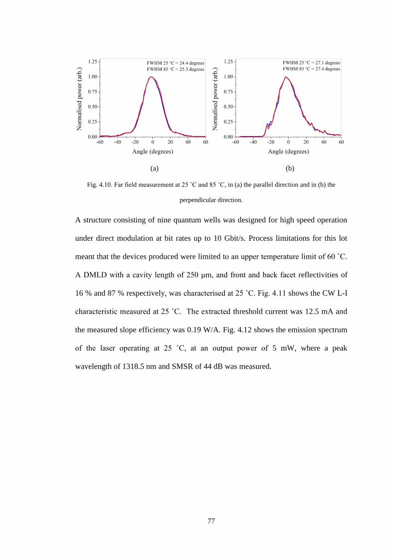
77
(a) (b)
Fig. 4.10. Far field measurement at 25 ˚C and 85 ˚C, in (a) the parallel direction and in (b) the
perpendicular direction.
A structure consisting of nine quantum wells was designed for high speed operation
under direct modulation at bit rates up to 10 Gbit/s. Process limitations for this lot
meant that the devices produced were limited to an upper temperature limit of 60 ˚C.
A DMLD with a cavity length of 250 μm, and front and back facet reflectivities of
16 % and 87 % respectively, was characterised at 25 ˚C. Fig. 4.11 shows the CW L-I
characteristic measured at 25 ˚C. The extracted threshold current was 12.5 mA and
the measured slope efficiency was 0.19 W/A. Fig. 4.12 shows the emission spectrum
of the laser operating at 25 ˚C, at an output power of 5 mW, where a peak
wavelength of 1318.5 nm and SMSR of 44 dB was measured.

78
Fig. 4.11. 1310 nm DMLD L-I characteristic measured at 25 ˚C.
Fig. 4.12. 1310 nm DMLD optical spectra measured at 25 ˚C.
The device’s modulation bandwidth was extracted by measuring the electro-optic
response, or S21, using a VNA, and is shown in Fig. 4.13. The device was packaged
in a high speed TO-can with a matching resistor to match the overall impedance to
50 Ω. From the S21 plot the 3 dB bandwidth value was extracted to give a value of
9 GHz at 20 mA and this increased to 15.1 GHz at 60 mA, indicating that the device
has the requisite bandwidth for operation at 10 Gbit/s.
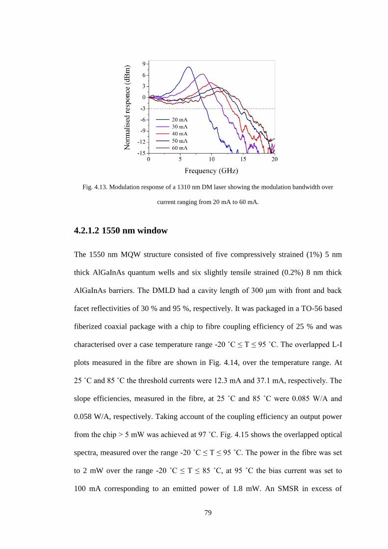
79
Fig. 4.13. Modulation response of a 1310 nm DM laser showing the modulation bandwidth over
current ranging from 20 mA to 60 mA.
4.2.1.2 1550 nm window
The 1550 nm MQW structure consisted of five compressively strained (1%) 5 nm
thick AlGaInAs quantum wells and six slightly tensile strained (0.2%) 8 nm thick
AlGaInAs barriers. The DMLD had a cavity length of 300 μm with front and back
facet reflectivities of 30 % and 95 %, respectively. It was packaged in a TO-56 based
fiberized coaxial package with a chip to fibre coupling efficiency of 25 % and was
characterised over a case temperature range -20 ˚C ≤ T ≤ 95 ˚C. The overlapped L-I
plots measured in the fibre are shown in Fig. 4.14, over the temperature range. At
25 ˚C and 85 ˚C the threshold currents were 12.3 mA and 37.1 mA, respectively. The
slope efficiencies, measured in the fibre, at 25 ˚C and 85 ˚C were 0.085 W/A and
0.058 W/A, respectively. Taking account of the coupling efficiency an output power
from the chip > 5 mW was achieved at 97 ˚C. Fig. 4.15 shows the overlapped optical
spectra, measured over the range -20 ˚C ≤ T ≤ 95 ˚C. The power in the fibre was set
to 2 mW over the range -20 ˚C ≤ T ≤ 85 ˚C, at 95 ˚C the bias current was set to
100 mA corresponding to an emitted power of 1.8 mW. An SMSR in excess of

80
40 dB was measured over the range -20 ˚C ≤ T ≤ 95 ˚C. The lasing wavelength
displayed a linear dependence with temperature corresponding to a tuning rate Δλ/ΔT
of 0.11 nm/˚C.
Fig. 4.14. 1550 nm DMLD module L-I plots over the range -20 ˚C ≤ T ≤ 95 ˚C.
Fig. 4.15. 1550 nm DMLD optical spectra measured over the range -20 ˚C ≤ T ≤ 95 ˚C.
Fig. 4.16 shows the far field in (a) the parallel and (b) perpendicular directions,
measured prior to packaging at 25 ˚C and 85 ˚C, with an output power from the chip
of 5 mW. The measurement shows that the beam remains stable over the temperature
range, with a value of 25.8 degrees measured in the parallel direction at both 25 ˚C
and 85 ˚C. In the perpendicular direction values of 29.1 degrees and 28.9 degrees
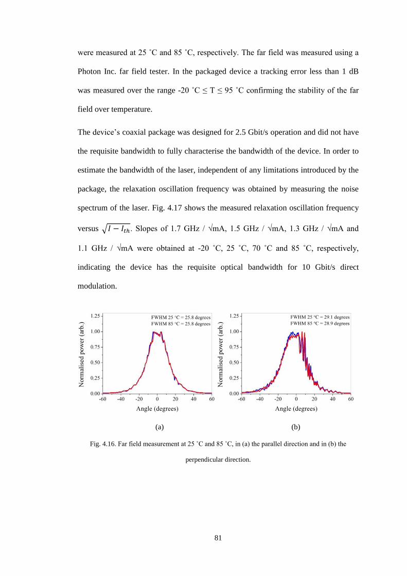
81
were measured at 25 ˚C and 85 ˚C, respectively. The far field was measured using a
Photon Inc. far field tester. In the packaged device a tracking error less than 1 dB
was measured over the range -20 ˚C ≤ T ≤ 95 ˚C confirming the stability of the far
field over temperature.
The device’s coaxial package was designed for 2.5 Gbit/s operation and did not have
the requisite bandwidth to fully characterise the bandwidth of the device. In order to
estimate the bandwidth of the laser, independent of any limitations introduced by the
package, the relaxation oscillation frequency was obtained by measuring the noise
spectrum of the laser. Fig. 4.17 shows the measured relaxation oscillation frequency
versus √ . Slopes of 1.7 GHz / √mA, 1.5 GHz / √mA, 1.3 GHz / √mA and
1.1 GHz / √mA were obtained at -20 ˚C, 25 ˚C, 70 ˚C and 85 ˚C, respectively,
indicating the device has the requisite optical bandwidth for 10 Gbit/s direct
modulation.
(a) (b)
Fig. 4.16. Far field measurement at 25 ˚C and 85 ˚C, in (a) the parallel direction and in (b) the
perpendicular direction.
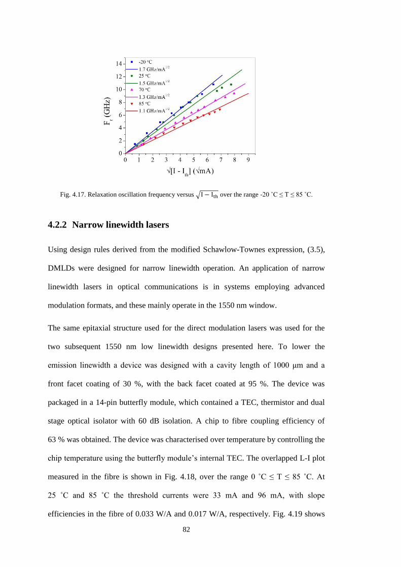
82
Fig. 4.17. Relaxation oscillation frequency versus √ over the range -20 ˚C ≤ T ≤ 85 ˚C.
4.2.2 Narrow linewidth lasers
Using design rules derived from the modified Schawlow-Townes expression, (3.5),
DMLDs were designed for narrow linewidth operation. An application of narrow
linewidth lasers in optical communications is in systems employing advanced
modulation formats, and these mainly operate in the 1550 nm window.
The same epitaxial structure used for the direct modulation lasers was used for the
two subsequent 1550 nm low linewidth designs presented here. To lower the
emission linewidth a device was designed with a cavity length of 1000 μm and a
front facet coating of 30 %, with the back facet coated at 95 %. The device was
packaged in a 14-pin butterfly module, which contained a TEC, thermistor and dual
stage optical isolator with 60 dB isolation. A chip to fibre coupling efficiency of
63 % was obtained. The device was characterised over temperature by controlling the
chip temperature using the butterfly module’s internal TEC. The overlapped L-I plot
measured in the fibre is shown in Fig. 4.18, over the range 0 ˚C ≤ T ≤ 85 ˚C. At
25 ˚C and 85 ˚C the threshold currents were 33 mA and 96 mA, with slope
efficiencies in the fibre of 0.033 W/A and 0.017 W/A, respectively. Fig. 4.19 shows
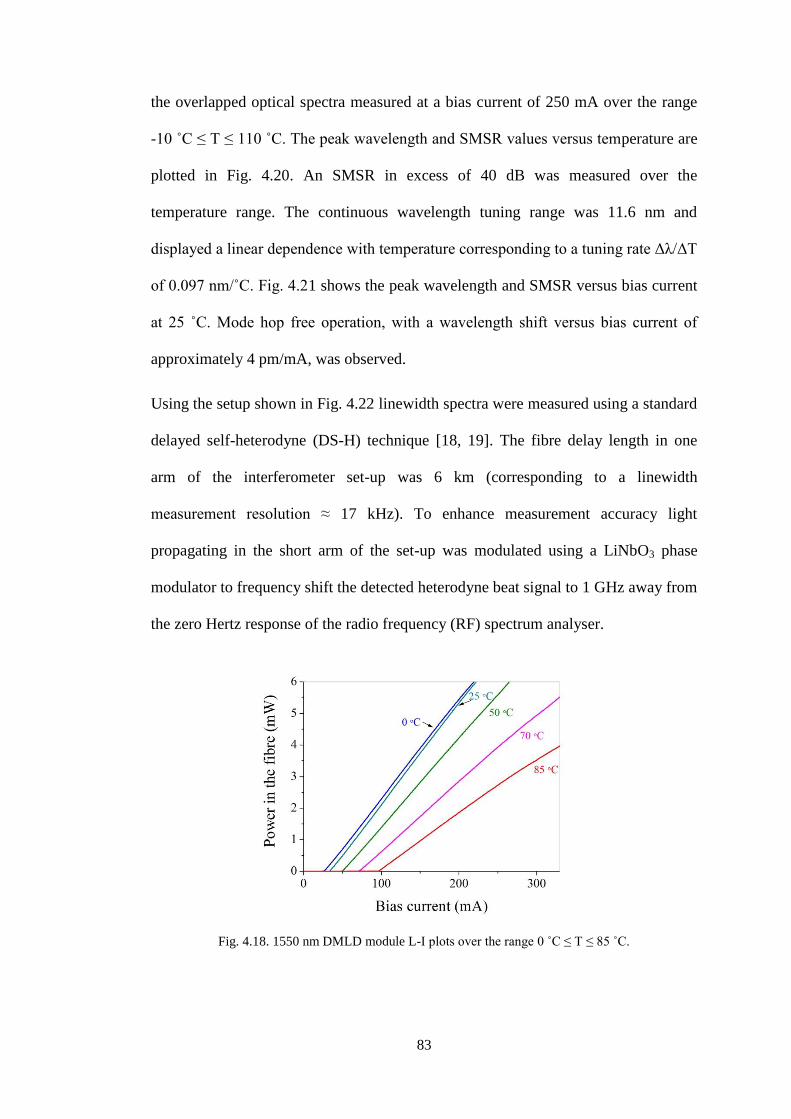
83
the overlapped optical spectra measured at a bias current of 250 mA over the range
-10 ˚C ≤ T ≤ 110 ˚C. The peak wavelength and SMSR values versus temperature are
plotted in Fig. 4.20. An SMSR in excess of 40 dB was measured over the
temperature range. The continuous wavelength tuning range was 11.6 nm and
displayed a linear dependence with temperature corresponding to a tuning rate Δλ/ΔT
of 0.097 nm/˚C. Fig. 4.21 shows the peak wavelength and SMSR versus bias current
at 25 ˚C. Mode hop free operation, with a wavelength shift versus bias current of
approximately 4 pm/mA, was observed.
Using the setup shown in Fig. 4.22 linewidth spectra were measured using a standard
delayed self-heterodyne (DS-H) technique [18, 19]. The fibre delay length in one
arm of the interferometer set-up was 6 km (corresponding to a linewidth
measurement resolution ≈ 17 kHz). To enhance measurement accuracy light
propagating in the short arm of the set-up was modulated using a LiNbO3 phase
modulator to frequency shift the detected heterodyne beat signal to 1 GHz away from
the zero Hertz response of the radio frequency (RF) spectrum analyser.
Fig. 4.18. 1550 nm DMLD module L-I plots over the range 0 ˚C ≤ T ≤ 85 ˚C.
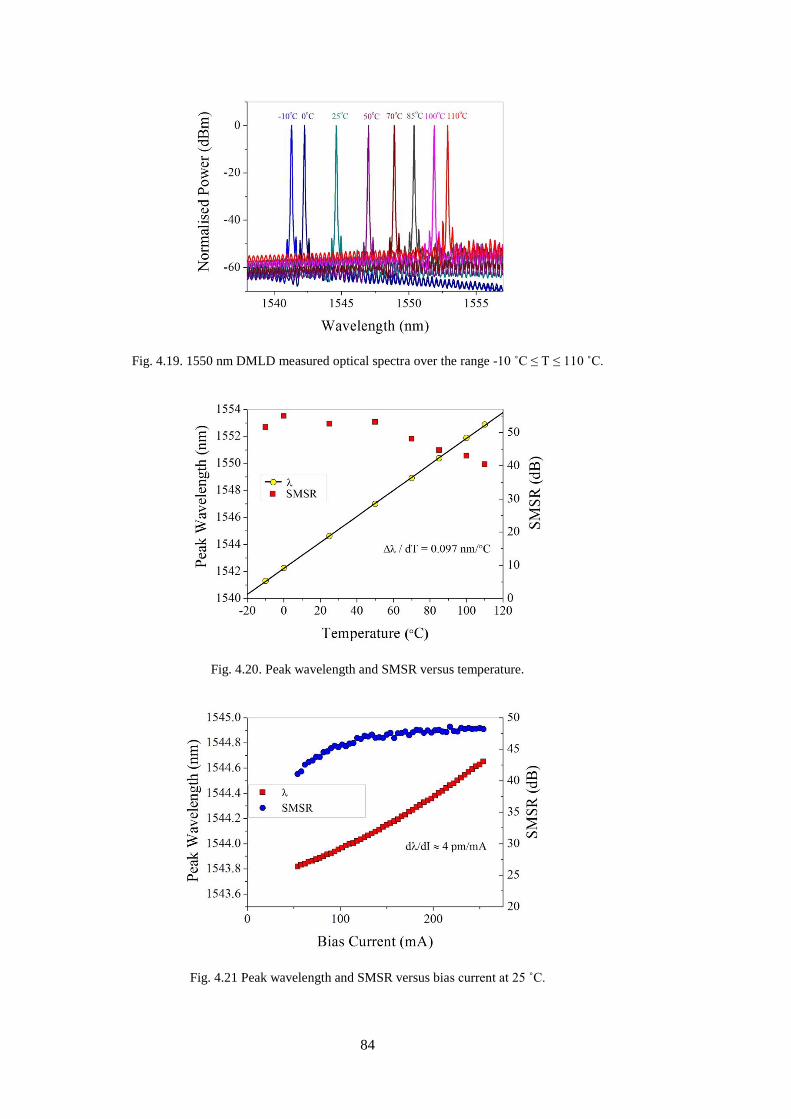
84
Fig. 4.19. 1550 nm DMLD measured optical spectra over the range -10 ˚C ≤ T ≤ 110 ˚C.
Fig. 4.20. Peak wavelength and SMSR versus temperature.
Fig. 4.21 Peak wavelength and SMSR versus bias current at 25 ˚C.

85
Fig. 4.22. Delayed self-heterodyne experimental set-up.
Fig. 4.23 shows the extracted Lorentzian component of the emission linewidth versus
inverse power in the fibre. A minimum linewidth of 138 kHz was measured at an
output power of 8.4 mW, and a corresponding bias current of 300 mA. The measured
DS-H spectrum was fitted to a Lorentzian lineshape to extract the half-width at half
maximum value, and is shown in Fig. 4.24, with the bias current set to 300 mA.
Fig. 4.25 shows the extracted Lorentzian component of the emission linewidth versus
temperature for two operating conditions; the first where the power in the fibre is
kept constant at 4 mW and the second where the bias current is kept constant at
250 mA. At a constant power of 4 mW a maximum linewidth of 235 kHz was
measured at 85 ˚C, and a minimum value of 212 kHz was measured at 25 ˚C,
corresponding to a variation in the linewidth of only 23 kHz over the range
0 ˚C ≤ T ≤ 85 ˚C. When the device is operated at a constant bias current of 250 mA a
linewidth below 200 kHz was measured over the range 0 ˚C ≤ T ≤ 60 ˚C. The
increase in linewidth at higher temperatures is due to the reduction in the optical
power for a given input current, leading to a reduction in the photon density in the
laser cavity. At temperatures below 0 ˚C and above 85 ˚C it was not possible to
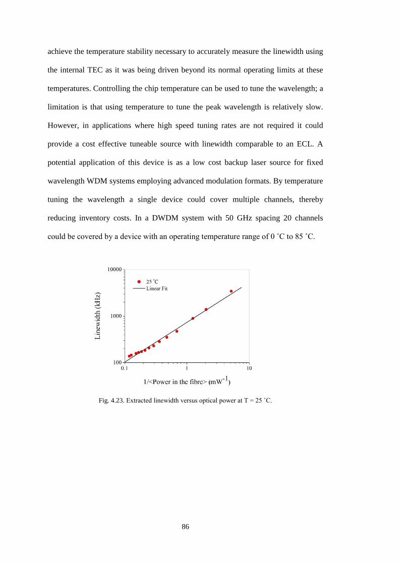
86
achieve the temperature stability necessary to accurately measure the linewidth using
the internal TEC as it was being driven beyond its normal operating limits at these
temperatures. Controlling the chip temperature can be used to tune the wavelength; a
limitation is that using temperature to tune the peak wavelength is relatively slow.
However, in applications where high speed tuning rates are not required it could
provide a cost effective tuneable source with linewidth comparable to an ECL. A
potential application of this device is as a low cost backup laser source for fixed
wavelength WDM systems employing advanced modulation formats. By temperature
tuning the wavelength a single device could cover multiple channels, thereby
reducing inventory costs. In a DWDM system with 50 GHz spacing 20 channels
could be covered by a device with an operating temperature range of 0 ˚C to 85 ˚C.
Fig. 4.23. Extracted linewidth versus optical power at T = 25 ˚C.
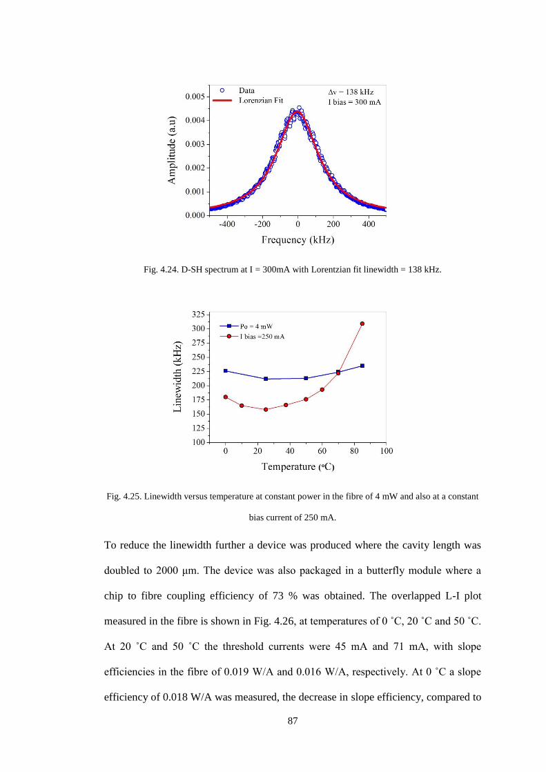
87
Fig. 4.24. D-SH spectrum at I = 300mA with Lorentzian fit linewidth = 138 kHz.
Fig. 4.25. Linewidth versus temperature at constant power in the fibre of 4 mW and also at a constant
bias current of 250 mA.
To reduce the linewidth further a device was produced where the cavity length was
doubled to 2000 μm. The device was also packaged in a butterfly module where a
chip to fibre coupling efficiency of 73 % was obtained. The overlapped L-I plot
measured in the fibre is shown in Fig. 4.26, at temperatures of 0 ˚C, 20 ˚C and 50 ˚C.
At 20 ˚C and 50 ˚C the threshold currents were 45 mA and 71 mA, with slope
efficiencies in the fibre of 0.019 W/A and 0.016 W/A, respectively. At 0 ˚C a slope
efficiency of 0.018 W/A was measured, the decrease in slope efficiency, compared to

88
that obtained at 20 ˚C, is due to a slight change in the alignment of the coupling
optics in the butterfly package at 0 ˚C, and a result of the TEC being operated below
the recommended operating temperature for this package. Fig. 4.27 shows the
overlapped optical spectra measured at a bias current of 300 mA over the range
-5 ˚C ≤ T ≤ 50 ˚C. An SMSR in excess of 40 dB was measured over the temperature
range. The peak wavelength and SMSR values versus temperature are plotted in
Fig. 4.28. An SMSR in excess of 40 dB was measured over the temperature range.
The continuous wavelength tuning range was 5.5 nm and displayed a linear
dependence with temperature corresponding to a tuning rate Δλ/ΔT of 0.1 nm/˚C.
Fig. 4.29 shows the peak wavelength and SMSR versus bias current at 20 ˚C. Mode
hop free operation, with a wavelength shift versus bias current of approximately
2 pm/mA, was observed. The reduction in this value, compared to the 1000 μm
device, is due to the longer cavity.
Fig. 4.26. 1550 nm DMLD module L-I plots measured at 0 ˚C, 20 ˚C and 50 ˚C.

89
Fig. 4.27. 1550 nm DMLD measured optical spectra over the range -5 ˚C ≤ T ≤ 50 ˚C.
Fig. 4.28. Peak wavelength and SMSR versus bias current at 20 ˚C.
Fig. 4.29. Peak wavelength and SMSR versus bias current at 20 ˚C.
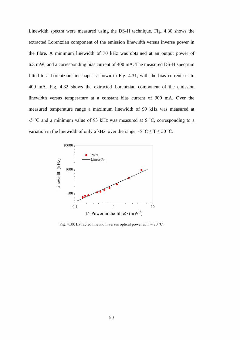
90
Linewidth spectra were measured using the DS-H technique. Fig. 4.30 shows the
extracted Lorentzian component of the emission linewidth versus inverse power in
the fibre. A minimum linewidth of 70 kHz was obtained at an output power of
6.3 mW, and a corresponding bias current of 400 mA. The measured DS-H spectrum
fitted to a Lorentzian lineshape is shown in Fig. 4.31, with the bias current set to
400 mA. Fig. 4.32 shows the extracted Lorentzian component of the emission
linewidth versus temperature at a constant bias current of 300 mA. Over the
measured temperature range a maximum linewidth of 99 kHz was measured at
-5 ˚C and a minimum value of 93 kHz was measured at 5 ˚C, corresponding to a
variation in the linewidth of only 6 kHz over the range -5 ˚C ≤ T ≤ 50 ˚C.
Fig. 4.30. Extracted linewidth versus optical power at T = 20 ˚C.

91
Fig. 4.31. D-SH spectrum at I = 400 mA with Lorenztian fit linewidth = 70 kHz.
Fig. 4.32. Linewidth versus temperature at a constant bias current of 300 mA.
From a coherent detection viewpoint having a knowledge of the frequency noise
spectrum is preferred over a simple linewidth number as it allows the source of the
noise to be identified and allows assessment of the extent to which detection
electronics can compensate for the phase noise. The phase noise power spectral
density (Sν (f), PSD) [20], was also measured for this laser. This measurement was
carried out in the optical communications optoelectronics research centre, University
of Southampton. The accuracy of the results obtained using this setup was verified
using other commercially available lasers, and in [21] this setup was used to

92
characterise four different types of lasers. A second reason for carrying out this
measurement was to compare the linewidth result obtained using this technique with
that obtained using the D-SH technique.
The experimental set-up for measuring Sν (f) is shown in Fig. 4.33. It consists of a
delayed balanced MZI that acts as a sensitive frequency-to-amplitude converter
followed by a DC-coupled photodetector and a fast Fourier transform (FFT)
spectrum analyser. The PSD measured with FFT spectrum analyser, (expressed in
V2/Hz), is related to Sν (f) by [20]:
fA
ffSfS SA 22
2
sin)()(
(4.12)
Here, f is the Fourier frequency, τ is the MZI time delay and A is the maximum peak-
to-peak (p-p) amplitude (in Volts) of the fringes seen on the interferometer. This
equation assumes that the intensity noise of the laser, the shot noise, and electronic
thermal noise are negligible compared to the converted frequency noise. The highest
sensitivity is obtained when 0sin f , which occurs when signal power at this
frequency is split equally into both arms of the output MZI coupler. During the
measurement the laser carrier frequency was maintained at this condition by
feedback control of a piezoelectric fibre stretcher placed inside one arm of the MZI
that allows for fine tuning of the time delay τ. The coarse setting of the time delay τ
is realized by inserting a length of fibre inside one arm of the MZI. The whole set-up
is implemented with polarization maintaining (PM) components in order to avoid
polarization fading/drift. A time delay τ of 6.5 ns (1.3 m fibre length) was chosen,
which was small enough to make the approximation
ff sin (4.13)

93
over the whole frequency range of interest (e.g., 0-10 MHz). Practically, this means
that there is constant sensitivity over the whole measurement range, which can be
easily appreciated by inserting (4.13) into (4.12) giving:
2
)()( AfSfS SA (4.14)
Sν(f), measured in Hz/√Hz, is shown in Fig. 4.34, over the frequency ranges 100 Hz
to 10 MHz in (a) and 1 kHz to 100 kHz in (b). It was measured by converting the
laser frequency noise into amplitude noise with the interferometer maintained in
quadrature. At low frequencies (1Hz-10kHz) the PSD has a 1/f behaviour. For higher
frequencies (10kHz-10MHz) the frequency noise forms a plateau. The white
frequency noise decreases as the bias current is increased as shown in Fig. 4.34 (a).
These measurements were processed to calculate the laser linewidth at the points
shown in Fig. 4.34 (b), values of 91 kHz and 67 kHz were extracted at bias currents
of 300 mA and 400 mA, respectively. This compares favourably with the D-SH
measurement where values of 94 kHz and 70 kHz were extracted at 300 mA and
400 mA, respectively.
Fig. 4.33. Measurement set-up for frequency noise PSD measurement based on frequency-to-
amplitude converter.

94
(a) (b)
Fig. 4.34. Overlapped frequency noise spectrum measured at (a) 200 mA, 300 mA and 400mA, over a
frequency range of 0.1 kHz to 10 MHz and (b) 300 mA and 400mA, over a frequency range of 1 kHz
to 100 kHz and showing extracted linewidth values.
4.2.3 Higher power lasers
DMLDs designed for higher output power, as well as low linewidth, were also
fabricated. In order to increase the optical power the number of quantum wells was
reduced to three and the thickness of the SCH was increased to expand the optical
mode at the facets, thereby reducing the optical intensity. Details of the layer
structure are as follows: the MQW structure consisted of three compressively
strained (1%) 6 nm-thick AlGaInAs quantum wells and four slightly tensile strained
(0.2%) 8 nm thick AlGaInAs barriers. The MQW was sandwiched between two
400 nm-thick InGaAsP SCH layers with a bandgap wavelength of λg = 1.3 μm,
which also acted as an etch stop layer for the ridge waveguide and slot definition. A
1.8 μm thick p-InP layer was grown on top of the SCH, followed by a 200 nm thick
highly p-doped InGaAs contact layer. The ridge waveguide width was 3 μm and the
laser had a cavity length of 1000 μm. Increased output power was also achieved by
reducing the front facet coating to 7 %, with the back facet coated at 95 %. The
DMLD was mounted p-side up on a C-mount. Light was coupled from the laser chip
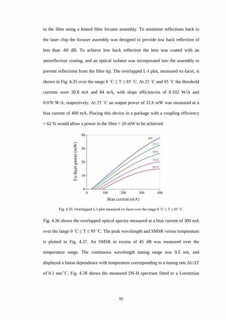
95
to the fibre using a lensed fibre focuser assembly. To minimise reflections back to
the laser chip the focuser assembly was designed to provide low back reflection of
less than -60 dB. To achieve low back reflection the lens was coated with an
antireflection coating, and an optical isolator was incorporated into the assembly to
prevent reflections from the fibre tip. The overlapped L-I plot, measured ex-facet, is
shown in Fig. 4.35 over the range 0 ˚C ≤ T ≤ 85 ˚C. At 25 ˚C and 85 ˚C the threshold
currents were 30.8 mA and 84 mA, with slope efficiencies of 0.102 W/A and
0.070 W/A, respectively. At 25 ˚C an output power of 32.6 mW was measured at a
bias current of 400 mA. Placing this device in a package with a coupling efficiency
> 62 % would allow a power in the fibre > 20 mW to be achieved.
Fig. 4.35. Overlapped L-I plot measured ex-facet over the range 0 ˚C ≤ T ≤ 85 ˚C.
Fig. 4.36 shows the overlapped optical spectra measured at a bias current of 300 mA
over the range 0 ˚C ≤ T ≤ 95 ˚C. The peak wavelength and SMSR versus temperature
is plotted in Fig. 4.37. An SMSR in excess of 45 dB was measured over the
temperature range. The continuous wavelength tuning range was 9.5 nm, and
displayed a linear dependence with temperature corresponding to a tuning rate Δλ/ΔT
of 0.1 nm/˚C. Fig. 4.38 shows the measured DS-H spectrum fitted to a Lorentzian

96
lineshape to extract the half-width at half maximum value. A value of 194 kHz was
obtained at 25 ˚C at a bias current of 300 mA.
Fig. 4.36. 1550 nm DMLD measured optical spectra over the range 0 ˚C ≤ T ≤ 95 ˚C.
Fig. 4.37. Peak wavelength and SMSR versus temperature.
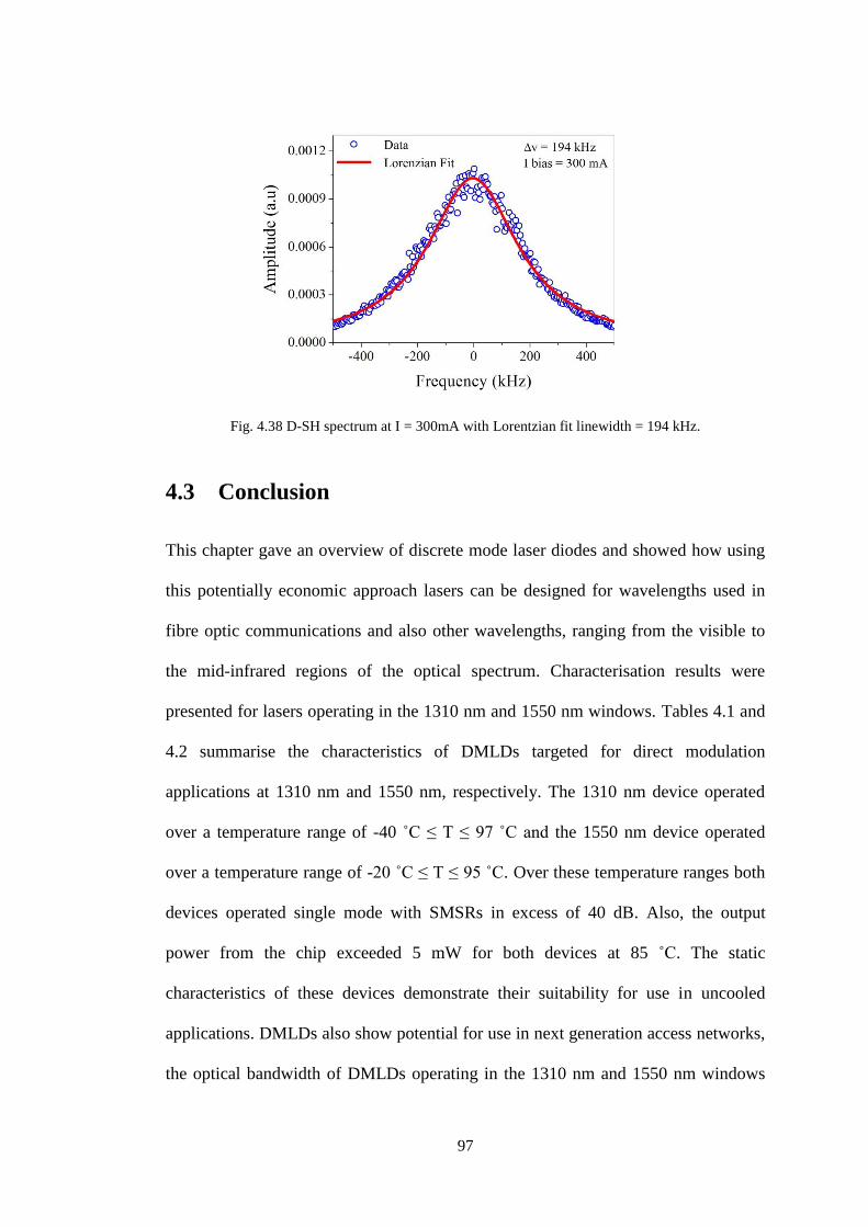
97
Fig. 4.38 D-SH spectrum at I = 300mA with Lorentzian fit linewidth = 194 kHz.
4.3 Conclusion
This chapter gave an overview of discrete mode laser diodes and showed how using
this potentially economic approach lasers can be designed for wavelengths used in
fibre optic communications and also other wavelengths, ranging from the visible to
the mid-infrared regions of the optical spectrum. Characterisation results were
presented for lasers operating in the 1310 nm and 1550 nm windows. Tables 4.1 and
4.2 summarise the characteristics of DMLDs targeted for direct modulation
applications at 1310 nm and 1550 nm, respectively. The 1310 nm device operated
over a temperature range of -40 ˚C ≤ T ≤ 97 ˚C and the 1550 nm device operated
over a temperature range of -20 ˚C ≤ T ≤ 95 ˚C. Over these temperature ranges both
devices operated single mode with SMSRs in excess of 40 dB. Also, the output
power from the chip exceeded 5 mW for both devices at 85 ˚C. The static
characteristics of these devices demonstrate their suitability for use in uncooled
applications. DMLDs also show potential for use in next generation access networks,
the optical bandwidth of DMLDs operating in the 1310 nm and 1550 nm windows
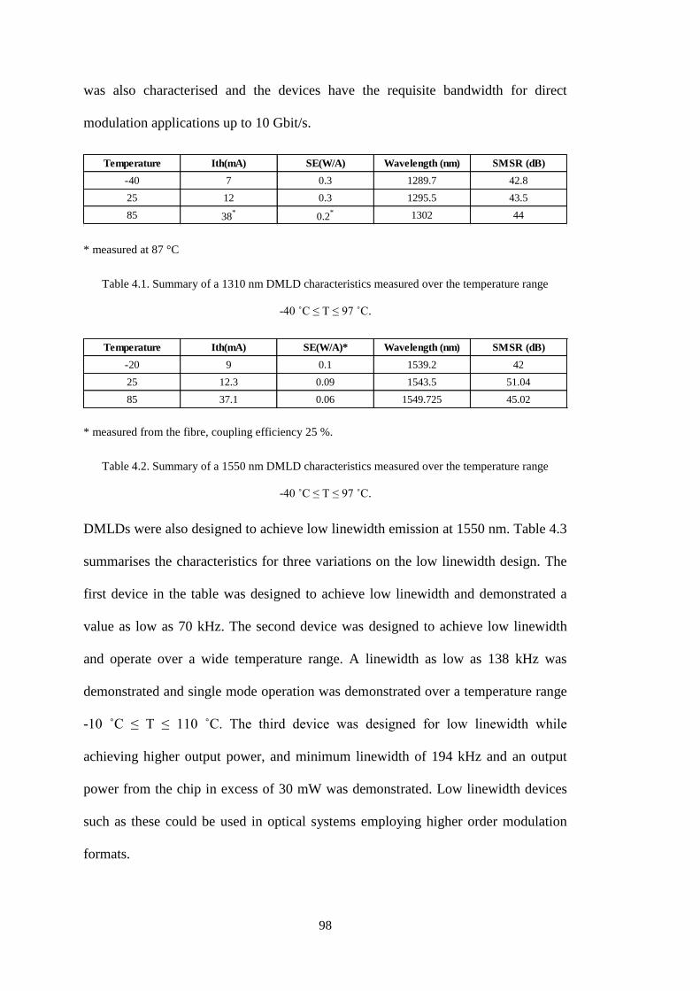
98
was also characterised and the devices have the requisite bandwidth for direct
modulation applications up to 10 Gbit/s.
* measured at 87 °C
Table 4.1. Summary of a 1310 nm DMLD characteristics measured over the temperature range
-40 ˚C ≤ T ≤ 97 ˚C.
* measured from the fibre, coupling efficiency 25 %.
Table 4.2. Summary of a 1550 nm DMLD characteristics measured over the temperature range
-40 ˚C ≤ T ≤ 97 ˚C.
DMLDs were also designed to achieve low linewidth emission at 1550 nm. Table 4.3
summarises the characteristics for three variations on the low linewidth design. The
first device in the table was designed to achieve low linewidth and demonstrated a
value as low as 70 kHz. The second device was designed to achieve low linewidth
and operate over a wide temperature range. A linewidth as low as 138 kHz was
demonstrated and single mode operation was demonstrated over a temperature range
-10 ˚C ≤ T ≤ 110 ˚C. The third device was designed for low linewidth while
achieving higher output power, and minimum linewidth of 194 kHz and an output
power from the chip in excess of 30 mW was demonstrated. Low linewidth devices
such as these could be used in optical systems employing higher order modulation
formats.
Temperature Ith(mA) SE(W/A) Wavelength (nm) SMSR (dB)
-40 7 0.3 1289.7 42.8
25 12 0.3 1295.5 43.5
85 38*
0.2* 1302 44
* measured at 87 °C
Temperature Ith(mA) SE(W/A)* Wavelength (nm) SMSR (dB)
-20 9 0.1 1539.2 42
25 12.3 0.09 1543.5 51.04
85 37.1 0.06 1549.725 45.02

99
Table 4.3. Summary of low linewidth DMLDs design parameters and the corresponding minimum
linewidth values demonstrated.
The next two chapters will focus on the characterisation of DMLDs in system level
experiments, utilising direct modulation and advanced modulation formats,
respectively.
References
[1] D. T. Cassidy and F. H. Peters, “Spontaneous emission, scattering, and the spectral
properities of semiconductor diode lasers,” IEEE Journal of Quantum Electronics, vol.
28, no. 4, pp. 785-791, Aprl. 1992.
[2] L. F. DeChiaro, “Damage-Induced Spectral Perturbations in Multilongitudinal-Mode
Semiconductor Lasers,” Journal of Lightwave Technology, vol. 8, no. 11, pp. 1659-
1669, Nov. 1990.
[3] L. F. DeChiaro, “Spectral width reduction in multilongitudinal mode lasers by spatial
loss profiling,” Journal of Lightwave Technology, vol. 9, no. 8, pp. 975-986, Aug.
1991.
[4] D. A. Kozlowski, J. S. Young, J. M. C. England and R. G. S. Plumb, “Longitudinal
mode control in 1.3 μm Fabry-Perot lasers by mode suppression,” IEE Proceedings-
Optoelectronics, vol. 143, no. 1, pp. 71-76, Feb. 1996.
[5] B. Corbett and D. McDonald, “ Single longitudinal mode ridge waveguide 1.3 μm
Fabry-Perot laser by modal perturbation,” Electronics Letters, vol. 31, no. 25, pp.
2181-2182, Dec. 1995.
[6] V. Weldon, J. O'Gorman, J. J. Perez-Camacho, D. McDonald, J. Hegarty and B.
Corbett, “Methane sensing with a novel micromachined single-frequency Fabry-Perot
laser diode emitting at 1331 nm,” IEEE Photonics Technology Letters , vol. 9, no. 3,
pp. 357-359, Mar. 1997.
Number of Quantum wells Coating front/back (%) Cavity length (µm) Minimum Linewidth @ 25 °C (kHz)
5 30/95 2000 70
5 30/95 1000 138
3 7/95 1000 194

100
[7] J. Patchell, D. Jones, B. Kelly and J. O’Gorman, “Specifying the wavelength and
temperature tuning range of a Fabry-Perot laser containing refractive index
perturbations,” Proceedings of SPIE, vol. 5825, pp. 1-13, Aprl. 2005.
[8] D. C. Byrne, PhD Thesis: An experimental investigation of tunable laser diodes based
on multiple etched slots, Dublin: Trinity College, 2010.
[9] D. C. Byrne, J. P. Engelstaedter, W. H. Guo, Y. L. Qiao, B. Corbett, B. Roycroft, J.
O'Callaghan, F. H. Peters and J. F. Donegan, “Discretely Tunable Semiconductor
Lasers Suitable for Photonic Integration,” IEEE Journal of Selected Topics in
Quantum Electronics, vol. 15, no. 3, pp. 482-487, Jun. 2009.
[10] L. A. Coldren, Diode Lasers and Photonic Integrated Circuits, Hoboken: Wiley, 2012.
[11] M. Fukuda, T. Mishima, N. Nakayama and T. Masuda, “Temperature and current
coefficients of lasing wavelength in tunable diode laser spectroscopy,” Applied
Physics B, vol. 100, no. 2, pp. 377-382, Aug. 2010.
[12] H. Lu, C. Blaauw and T. Makino, “Single-mode operation over a wide temperature
range in 1.3 μm InGaAsP/InP distributed feedback lasers,” Journal of Lightwave
Technology, vol. 14, no. 5, pp. 851-859, May 1996.
[13] F. Gruet, T. Bandi, G. Mileti, R. Phelan, J. O'Carroll, B. Kelly and J. O'Gorman,
“Development and spectral characterisation of discrete mode laser diodes (DMLDs)
emitting at 780 nm for Rubidium atomic clocks,” in Lasers and Electro-Optics Europe
Conference (CLEO), Munich, May 2011.
[14] R. Phelan, J. O'Carroll, D. Byrne, C. Herbert, J. Somers and B. Kelly,
“In0.75Ga0.25As/InP Multiple Quantum Well Discrete Mode Laser Diode Emitting at
2 um,” IEEE Photonics Technology Letters, vol. 24, no. 8, pp. 652-654, Aprl. 2012.
[15] R. Phelan, T. J. Slight, B. Kelly, J. O'Carroll, A. McKee, D. G. Revin, S. Y. Zhang, A.
B. Krysa, K. L. Kennedy, J. W. Cockburn, C. N. Ironside, W. Meredith and J.
O'Gorman, “Room-Temperature Operation of Discrete-Mode InGaAs–AlAsSb
Quantum-Cascade Laser With Emission at λ =3.3 μm,” IEEE Photonics Technology
Letters, vol. 22, no. 17, pp. 1273-1275, Sept. 2010.
[16] H. Venghaus and N. Grote, Fibre Optic Communication key devices, Berlin: Springer,
2012.
[17] Integra Networks, “News articles: operating temperatures for fiber optic devices,” May
2012. [Online]. Available: http://integranetworks.net/2012/05/operating-temperatures-
for-fiber-optic-devices/.

101
[18] T. Okoshi, K. Kikuchi and A. Nakayama, “Novel method for high resolution
measurement of laser output spectrum,” Electronics Letters, vol. 16, no. 16, pp. 630-
631, Jul. 1980.
[19] M. O. van-Deventer, P. Spano and S. K. Nielsen, “Comparison of DFB laser linewidth
measurement techniques results from COST 215 round robin,” Electronics Letters,
vol. 26, no. 24, pp. 2018-2020, Nov. 1990.
[20] G. M. Stéphan, T. T. Tam, S. Blin, P. Besnard and M. Têtu, “Laser line shape and
spectral density of frequency noise,” Physical Review A, vol. 71, no. 4, pp. 0438091-
0438099, Aprl. 2005.
[21] R. Slavík, Y. Liao, E. Austin, P. Petropoulos and D. J. Richardson, “Full
characterization and comparison of phase properties of narrow linewidth lasers
operating in the C-band,” in International Conference on Optical Fiber Sensors,
Ottawa, May. 2011.

102

103
Chapter 5
Direct modulation of discrete
mode laser diodes
This chapter looks at the performance of discrete mode laser diodes under direct
modulation at a bit rate of 10 Gbit/s. Results are presented for lasers operating in
both the 1310 nm and 1550 nm wavelength windows, and includes the transmission
performance over single mode fibre.
5.1 1310 nm DMLD
1310 nm directly modulated single mode lasers capable of operating at 10 Gbit/s are
of interest for next generation access networks. Transmission distances of 10 km and
20 km are specified for Ethernet 10GBase-LR and 10GBase-LW, respectively. The
performance of a 1310 nm DMLD is characterised and its performance is evaluated
for use in 10 Gbit/s applications.
The nine quantum well 1310 nm DMLD presented in 4.2.1.1 was packaged in a high
speed TO-can package, where an internal resistor matched the impedance to 50 Ω
and single-ended modulation was used. Light was coupled to a fibre via a lensed

104
coupler on a precision x, y, z translation stage and a coupling efficiency of
approximately 10 % was achieved. The laser was modulated at 10 Gbit/s using a
pseudo random binary sequence (PRBS) pattern of 223
-1. PRBS patterns of 215
-1 and
223
-1 have been adopted by international standards [1], and 223
-1 was chosen as
longer patterns contain more frequency components, due to longer sequences of
continuous ‘1’s and ‘0’s. The DC bias current was set to 40 mA and the modulation
current was set to 40 mA p-p. An average optical power of 5.5 mW was measured
ex-facet and an extinction ratio of 6 dB was obtained. Fig. 5.1 shows the overlapped
spectra with the modulation on (white trace) and off (black trace) measured at a span
of (a) 40 nm and (b) 1 nm. The resolution of the optical spectrum analyser (OSA)
was set to 0.02 nm for the measurement. A peak wavelength of 1318.68 nm and
1318.64 nm was measured with the modulation on and off, respectively, and an
SMSR of 44.7 dB was measured for both conditions, demonstrating the stability of
the laser’s spectrum under modulation. The width of the peak, measured 20 dB
down, was 0.078 nm for the modulation turned off, and this increased to 0.172 nm
when the modulation was turned on. The value taken with the modulation turned off
was limited by the resolution of the OSA.

105
(a) (b)
Fig. 5.1. Overlapped optical spectra for a 1310 nm DMLD at 25 ˚C, with modulation current on and
off, measured at a wavelength span of (a) 40 nm and (b) 1 nm.
Using the setup shown in Fig. 5.2, the device was characterised back-to-back and
after transmission through 10 km and 22 km of SSMF, at a temperature of 25 ˚C. The
receiver used an unamplified PIN photo-detector with a 7.46 GHz low pass Bessel
Thompson filter applied to the output. Clock recovery was used for the transmission
experiments. Fig. 5.3 shows the eye diagram measured back-to-back, and a clear eye
opening is shown. Fig. 5.4 shows the BER versus received optical power measured
back-to-back and after transmission through 10 km and 22 km of SSMF. Relatively
low power penalties of 0.25 dB and 0.3 dB were measured after transmission through
10 km and 22 km, respectively, and no error floor was observed. The experiment
confirms that the laser is capable of achieving 10 Gbit/s transmission. The device
was not tested at 85 ˚C as it did not maintain single mode operation at higher
temperatures.
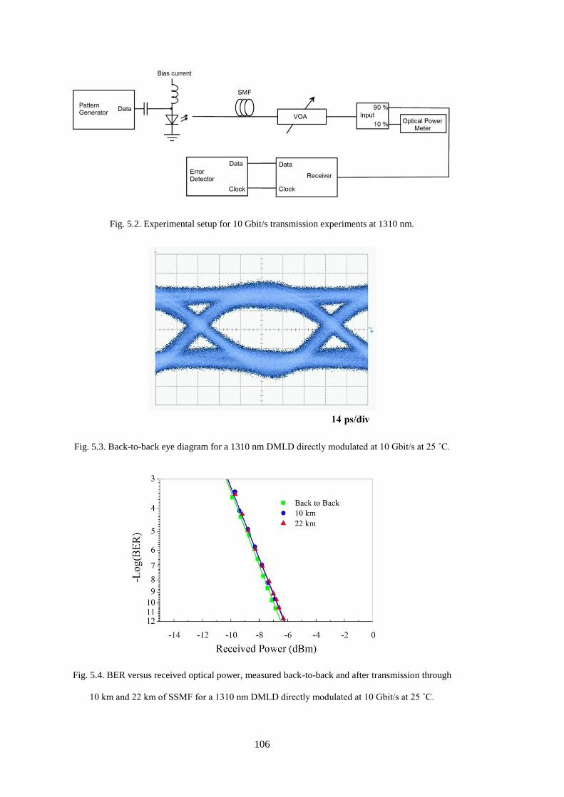
106
Fig. 5.2. Experimental setup for 10 Gbit/s transmission experiments at 1310 nm.
Fig. 5.3. Back-to-back eye diagram for a 1310 nm DMLD directly modulated at 10 Gbit/s at 25 ˚C.
Fig. 5.4. BER versus received optical power, measured back-to-back and after transmission through
10 km and 22 km of SSMF for a 1310 nm DMLD directly modulated at 10 Gbit/s at 25 ˚C.
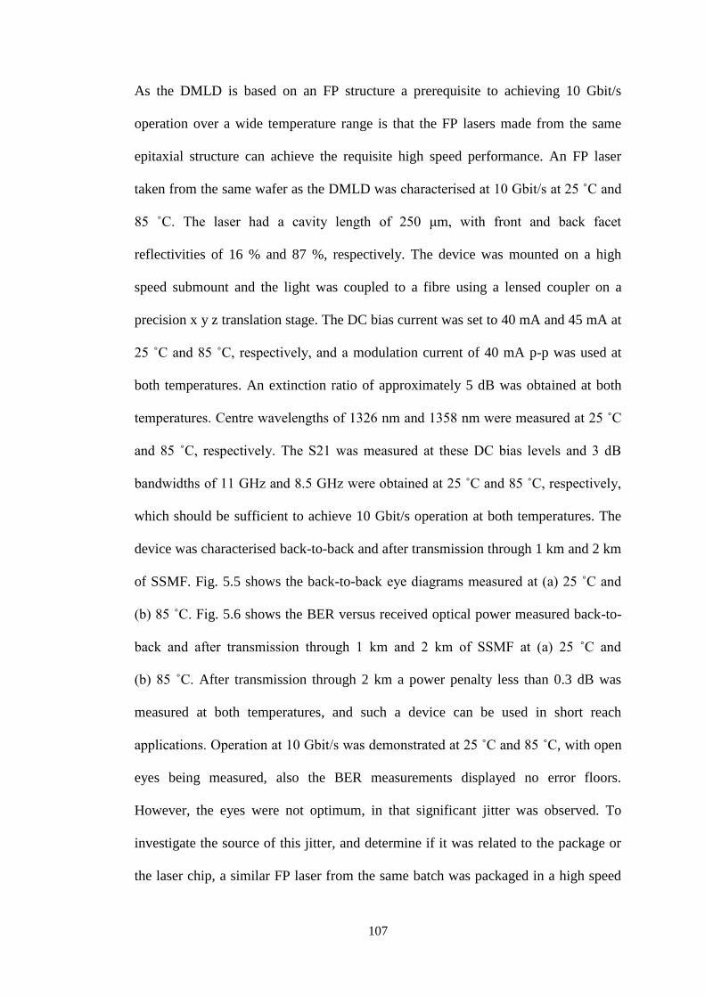
107
As the DMLD is based on an FP structure a prerequisite to achieving 10 Gbit/s
operation over a wide temperature range is that the FP lasers made from the same
epitaxial structure can achieve the requisite high speed performance. An FP laser
taken from the same wafer as the DMLD was characterised at 10 Gbit/s at 25 ˚C and
85 ˚C. The laser had a cavity length of 250 μm, with front and back facet
reflectivities of 16 % and 87 %, respectively. The device was mounted on a high
speed submount and the light was coupled to a fibre using a lensed coupler on a
precision x y z translation stage. The DC bias current was set to 40 mA and 45 mA at
25 ˚C and 85 ˚C, respectively, and a modulation current of 40 mA p-p was used at
both temperatures. An extinction ratio of approximately 5 dB was obtained at both
temperatures. Centre wavelengths of 1326 nm and 1358 nm were measured at 25 ˚C
and 85 ˚C, respectively. The S21 was measured at these DC bias levels and 3 dB
bandwidths of 11 GHz and 8.5 GHz were obtained at 25 ˚C and 85 ˚C, respectively,
which should be sufficient to achieve 10 Gbit/s operation at both temperatures. The
device was characterised back-to-back and after transmission through 1 km and 2 km
of SSMF. Fig. 5.5 shows the back-to-back eye diagrams measured at (a) 25 ˚C and
(b) 85 ˚C. Fig. 5.6 shows the BER versus received optical power measured back-to-
back and after transmission through 1 km and 2 km of SSMF at (a) 25 ˚C and
(b) 85 ˚C. After transmission through 2 km a power penalty less than 0.3 dB was
measured at both temperatures, and such a device can be used in short reach
applications. Operation at 10 Gbit/s was demonstrated at 25 ˚C and 85 ˚C, with open
eyes being measured, also the BER measurements displayed no error floors.
However, the eyes were not optimum, in that significant jitter was observed. To
investigate the source of this jitter, and determine if it was related to the package or
the laser chip, a similar FP laser from the same batch was packaged in a high speed
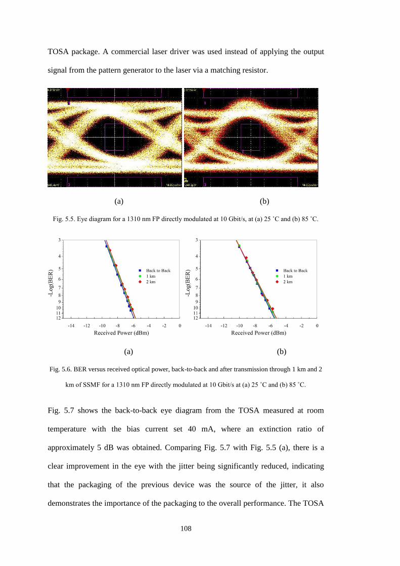
108
TOSA package. A commercial laser driver was used instead of applying the output
signal from the pattern generator to the laser via a matching resistor.
(a) (b)
Fig. 5.5. Eye diagram for a 1310 nm FP directly modulated at 10 Gbit/s, at (a) 25 ˚C and (b) 85 ˚C.
(a) (b)
Fig. 5.6. BER versus received optical power, back-to-back and after transmission through 1 km and 2
km of SSMF for a 1310 nm FP directly modulated at 10 Gbit/s at (a) 25 ˚C and (b) 85 ˚C.
Fig. 5.7 shows the back-to-back eye diagram from the TOSA measured at room
temperature with the bias current set 40 mA, where an extinction ratio of
approximately 5 dB was obtained. Comparing Fig. 5.7 with Fig. 5.5 (a), there is a
clear improvement in the eye with the jitter being significantly reduced, indicating
that the packaging of the previous device was the source of the jitter, it also
demonstrates the importance of the packaging to the overall performance. The TOSA

109
was not used for the initial work as this was carried out on a small number of devices
and the TOSA process is geared towards higher volumes.
Fig. 5.7. Eye diagram for a 1310 nm FP TOSA directly modulated at 10 Gbit/s, at room temperature.
5.2 1550 nm DMLD
The 1550 nm DMLD presented in 4.2.1.2 was packaged in a TO-56 based package;
however, this package did not have the required electrical bandwidth to investigate
the dynamic performance at 10 Gbit/s. To characterise the performance at 1550 nm a
DMLD in a more advanced package was used. The device had the same epitaxial
structure as the device presented in 4.2.1.2 but had a cavity length of 400 μm with
front and back facet reflectivities of 30 %. The package was a fiberized high speed
butterfly package with the modulation signal applied via a K type connector. An
internal resistor in the RF transmission line matched the impedance to 50 Ω, and
single-ended modulation was used. The laser chip temperature was set to 25 ˚C and
the device was modulated at a bit rate of 10 Gbit/s using a PRBS 223
-1 pattern. The
DC bias current was set to 60 mA and a modulation current of 40 mA p-p was used
to obtain an extinction ratio of 5.5 dB. Fig. 5.8 shows the overlapped spectra with the
modulation turned on (white trace), and off (black trace), at a wavelength span of
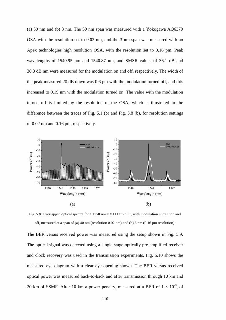
110
(a) 50 nm and (b) 3 nm. The 50 nm span was measured with a Yokogawa AQ6370
OSA with the resolution set to 0.02 nm, and the 3 nm span was measured with an
Apex technologies high resolution OSA, with the resolution set to 0.16 pm. Peak
wavelengths of 1540.95 nm and 1540.87 nm, and SMSR values of 36.1 dB and
38.3 dB nm were measured for the modulation on and off, respectively. The width of
the peak measured 20 dB down was 0.6 pm with the modulation turned off, and this
increased to 0.19 nm with the modulation turned on. The value with the modulation
turned off is limited by the resolution of the OSA, which is illustrated in the
difference between the traces of Fig. 5.1 (b) and Fig. 5.8 (b), for resolution settings
of 0.02 nm and 0.16 pm, respectively.
(a) (b)
Fig. 5.8. Overlapped optical spectra for a 1550 nm DMLD at 25 ˚C, with modulation current on and
off, measured at a span of (a) 40 nm (resolution 0.02 nm) and (b) 3 nm (0.16 pm resolution).
The BER versus received power was measured using the setup shown in Fig. 5.9.
The optical signal was detected using a single stage optically pre-amplified receiver
and clock recovery was used in the transmission experiments. Fig. 5.10 shows the
measured eye diagram with a clear eye opening shown. The BER versus received
optical power was measured back-to-back and after transmission through 10 km and
20 km of SSMF. After 10 km a power penalty, measured at a BER of 1 × 10⁻⁹
, of

111
0.8 dB was observed. After transmission through 20 km this increased to 5.3 dB,
also, the change in the slope of the 20 km data indicates the presence of an error
floor. The degradation in performance is the result of dispersion effects after
transmission through SSMF.
Fig. 5.9. Experimental setup for 10 Gbit/s transmission experiments at 1550 nm.
Fig. 5.10. Back-to-back eye diagram for a 1550 nm DMLD directly modulated at 10 Gbit/s at 25 ˚C.

112
Fig. 5.11. BER versus received optical power, measured back-to-back and after transmission through
10 km and 20 km of SSMF for a 1550 nm DMLD directly modulated at 10 Gbit/s at 25 ˚C.
5.2.1 10 Gbit/s transmission at 1550 nm with dispersion
compensation
Dispersion compensation modules can be used to extend the reach of directly
modulated lasers. In this experiment a dispersion compensation module with a
dispersion value of -681 ps/nm was introduced to the setup shown in Fig. 5.9, and
was placed directly after the laser. This provided pre-compensation for dispersion at
the transmitter allowing the reach to be extended. Fig. 5.12 shows the BER versus
received optical power measured back-to-back and after transmission through SSMF
for distances of 10 km, 22 km, 37 km, 49 km and 60 km. The back-to-back BER
measurement was taken at the output of the dispersion compensating module, and in
this case the laser together with the dispersion compensating module is considered to
be the transmitter. A maximum power penalty of 3.6 dB was measured at 60 km and
an increase in sensitivity, compared to the back-to-back measurement, was observed
at 10 km and 22 km indicating that the received signal was close to an optimum
value. Also, comparing the back-to-back case with dispersion compensation to that

113
of Fig. 5.11 for the laser on its own, there was an improvement in sensitivity of
2.2 dB. Previous work has shown that negative dispersion can lead to an
improvement in receiver sensitivity, as a result of pulse shaping due to the combined
effect of the chirp introduced by the laser and negative dispersion [2, 3]. Fig. 5.13
shows the BER versus received power measured after transmission through 37 km of
SSMF using dispersion pre-compensation and also using post compensation, where
the dispersion compensation module was moved and placed before the receiver;
negligible differences in the BER performance was observed between both cases.
Fig. 5.12. BER versus received optical power with dispersion pre-compensation of -681
ps/nm, measured back-to-back and after transmission through 10, 22, 37, 49 and 60 km of
SSMF. Inset: table listing the power penalties at the transmission distances measured.
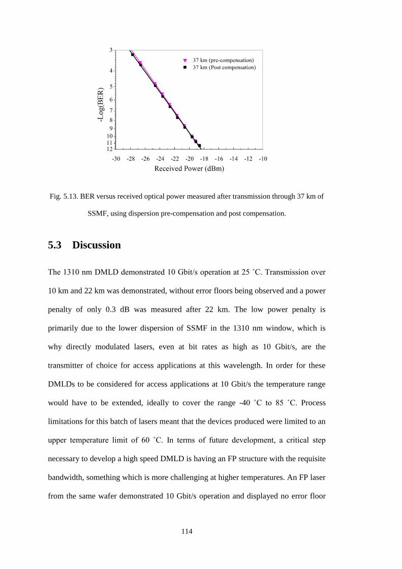
114
Fig. 5.13. BER versus received optical power measured after transmission through 37 km of
SSMF, using dispersion pre-compensation and post compensation.
5.3 Discussion
The 1310 nm DMLD demonstrated 10 Gbit/s operation at 25 ˚C. Transmission over
10 km and 22 km was demonstrated, without error floors being observed and a power
penalty of only 0.3 dB was measured after 22 km. The low power penalty is
primarily due to the lower dispersion of SSMF in the 1310 nm window, which is
why directly modulated lasers, even at bit rates as high as 10 Gbit/s, are the
transmitter of choice for access applications at this wavelength. In order for these
DMLDs to be considered for access applications at 10 Gbit/s the temperature range
would have to be extended, ideally to cover the range -40 ˚C to 85 ˚C. Process
limitations for this batch of lasers meant that the devices produced were limited to an
upper temperature limit of 60 ˚C. In terms of future development, a critical step
necessary to develop a high speed DMLD is having an FP structure with the requisite
bandwidth, something which is more challenging at higher temperatures. An FP laser
from the same wafer demonstrated 10 Gbit/s operation and displayed no error floor
115
in the BER measurement at both 25 ˚C and 85 ˚C, and this structure could be used in
future 10 Gbit/s DMLD development runs.
The 1550 nm DMLD demonstrated 10 Gbit/s operation at 25 ˚C. An open eye was
measured and the BER versus received optical power was measured back-to-back
and after transmission through 10 km and 20 km of SSMF. The power penalties,
measured at a BER of 1 × 10⁻⁹
, were 0.8 dB and 5.3 dB after transmission through
10 km and 20 km of SSMF, respectively. The increase in the power penalty after
20 km was due to chirp from the laser in combination with increased dispersion in
SSMF in the 1550 nm window. No error floor was observed in the back-to-back or
the 10 km measurement. The device could potentially be used as a transmitter laser
in links up to 10 km, but for transmission distances of 20 km, and beyond, more
advanced solutions need to be used for operation at 10 Gbit/s. One approach is to use
dispersion compensation, where negative dispersion is used to compensate for the
positive dispersion introduced by the SSMF. Negative dispersion can be introduced
to a link by adding dispersion compensating fibre (DCF) or lumped elements, such as
fibre Bragg gratings [4]. A dispersion compensating module, consisting of DCF, was
introduced to the setup and enabled the transmission distance to be extended to
60 km. In the experiment transmission over distances ranging from 10 km to 60 km
with a maximum power penalty of 3.6 dB was demonstrated. As the dispersion
compensation was placed in a pre-compensation configuration, such a scheme could
be used in a point to multi-point link. However, such a scheme may find limited
applications in access networks operating at 10 Gbit/s, as an EML with its lower
chirp may be a more practical solution. However, the use of directly modulated lasers
and dispersion compensation may be viable in an access system employing WDM, as
the dispersion compensation module would be shared between multiple channels [5].
116
Another development which could make the use of 1550 nm directly modulated
lasers a viable solution is electronic dispersion compensation. Pre-compensation pre-
distorts the drive signal applied to the laser and has the potential to extend the reach
significantly [6]. Electronic dispersion compensation can also be applied at the
receiver, where it could potentially double the transmission distance achievable [7].
The DMLD used at 1550 nm was primarily chosen because it was in a suitable high
speed package. The design was not optimum for high speed operation and it would
have been desirable to have used a device with a shorter cavity and a high reflectivity
coating on the back facet, as this would have increased the relaxation oscillation
frequency. The SMSR for the device exceeded 30 dB; however, as demonstrated in
4.2.1.2, it is possible to achieve an SMSR in excess of 40 dB from a 1550 nm
DMLD. Despite this, the device demonstrated 10 Gbit/s operation, showing that the
structure is capable of high speed operation. Also, optimised devices have the
potential to achieve improved performance, and this is an objective for future work
in this area. High speed lasers are also essential components for other applications, in
one example demonstrated in other work, a DMLD was gain switched at a frequency
of 10.7 GHz in order to generate a coherent optical multicarrier signal with a
frequency spacing between the side bands of 10.7 GHz [8]. Such a device could
potentially be used in a range of applications including optical arbitrary waveform
generation, photonic microwave signal generation, optical signal processing and
multicarrier spectrally efficient transmission techniques with the sub-channel spacing
equal to the symbol rate of each sub-channel [9].

117
5.4 Conclusion
10 Gbit/s operation was demonstrated using DMLDs at wavelengths in the 1310 nm
and 1550 nm windows. Transmission distances up to 22 km and 10 km were
demonstrated at 1310 nm and 1550 nm, respectively, without dispersion
compensation. Table 5.1 summarises the results after transmission through SSMF at
1310 nm. A maximum power penalty of only 0.3 dB was observed after 22 km and
the device shows potential for use in future access networks operating at 10 Gbit/s.
Table 5.2 summarises the results after transmission through SSMF at 1550 nm. A
maximum power penalty of 0.8 dB was observed after 10 km and this increased to
5.3 dB after transmission through 20 km. Such a device may find application in short
reach applications at 10 km, or less, operating at 10 Gbit/s. To increase the
transmission distance dispersion compensation would be necessary and it was shown
that the transmission distance could be extended to 60 km at 1550 nm using
dispersion compensation.
The next chapter will look at another application of single mode laser in fibre optic
communications, namely coherent communications, where the laser is operated CW
and external modulation is used.
Table 5.1. Summary of the transmission experiment results at 1310 nm.
Distance (km) Power penalty (dB) Comment
Back-to-back - Error free
10 0.25 Error free
22 0.3 Error free

118
Table 5.2. Summary of the transmission experiment results at 1550 nm.
References
[1] D. Derickson, Fiber Optic Test and Measurement, New Jersey: Prentice Hall, 1998.
[2] Y. Miyamoto, K. Hagimoto, F. Ichikawa, M. Yamamoto and T. Kagawa, “10 Gbit/s,
50 km dispersive fibre transmission experiment using strained multiquantum-well
DFB laser diode,” Electronics Letters, vol. 27, no. 10, pp. 853-855, May 1991.
[3] K. Sato, S. Kuwahara and Y. Miyamoto, “Chirp Characteristics of 40-Gb/s Directly
Modulated Distributed-Feedback Laser Diodes,” Journal of Lightwave Technology,
vol. 23, no. 11, pp. 3790-3797, Nov. 2005.
[4] J. M. Senior, Optical Fiber Communications: Principles and Practice, 3rd ed., New
York: Prentice Hall, 2009.
[5] X. Cheng, Y. J. Wen, Z. Xu, X. Shao, Y. Wang and Y. Yeo, “10-Gb/s WDM-PON
transmission using uncooled, directly modulated free-running 1.55-μm VCSELs,” in
European Conference on Optical Communication (ECOC), Brussels, Sept. 2008.
[6] A. S. Karar, J. C. Cartledge, J. Harley and K. Roberts, “Electronic Pre-Compensation
for a 10.7-Gb/s System Employing a Directly Modulated Laser,” Journal of Lightwave
Technology, vol. 29, no. 13, pp. 2069-2076, Jul. 2011.
[7] M. D. Feuer, H. Sun-Yuan, S. L. Woodward, O. Coskun and M. Boroditsky,
“Electronic dispersion compensation for a 10-Gb/s link using a directly modulated
laser,” IEEE Photonics Technology Letters, vol. 15, no. 12, pp. 1788-1790, Dec. 2003.
[8] P. M. Anandarajah, R. Maher, Y. Q. Xu, S. Latkowski, J. O'Carroll, S. G. Murdoch, R.
Phelan, J. O'Gorman and L. P. Barry, “Generation of Coherent Multicarrier Signals by
Gain Switching of Discrete Mode Lasers,” IEEE Photonics Journal, vol. 3, no. 1, pp.
112-122, Feb. 2011.
[9] R. Zhou, S. Latkowski, J. O'Carroll, R. Phelan, L. P. Barry and P. Anandarajah, “40nm
wavelength tunable gain-switched optical comb source,” in European Conference and
Exhibition on Optical Communication (ECOC), Geneva, Sept. 2011.
Distance (km) Power penalty (dB) Comment
Back-to-back - Error free
10 0.8 Error free
20 5.3 Error floor observed

119
Chapter 6
Characterisation of discrete
mode laser diodes in advanced
modulation format systems
In this chapter discrete mode laser diodes designed for narrow linewidth emission are
characterised in a test bed employing advanced modulation formats. Two formats are
considered, QPSK and 16-QAM, and the performance achieved using low linewidth
discrete mode laser diodes and an external cavity laser is compared. QPSK was
chosen as it has been widely used in current state of the art commercially deployed
systems [1, 2]. Compared to QPSK, 16-QAM has the potential to double capacity
while maintaining the same baud rate making it attractive for use in future coherent
systems [3]. Increasing the order of the modulation format places more stringent
requirements on the phase noise of the lasers used in these systems. The performance
of low linewidth DMLDs is evaluated through system experiments employing both
modulation formats and the results compared with those obtained using an ECL. The

120
effect of increased linewidth on the performance of these systems is also
investigated.
6.1 Experimental setup
The back-to-back coherent transmission setup is shown in Fig. 6.1. To generate the
electrical QPSK modulation signal, the data and data-bar outputs from a pattern
generator were used. The output for the pattern generator was 2 V p-p, however this
was insufficient to drive the IQ modulator which required a minimum drive voltage
of 3.5 V p-p [4]. Modulator drivers were used to amplify the pattern generator’s
outputs. The data pattern used was PRBS 29-1. A delay of 5.2 ns, corresponding to
13 symbols at 2.5 Gbaud, was applied to the data-bar signal decorrelating the data
patterns in order to emulate two independent channels. The data and data-bar signals
were then applied to the I and Q inputs of a dual parallel MZM, respectively. The IQ
modulator is a polarisation sensitive device, therefore, a polarisation controller was
placed at the modulators input to optimise the polarisation of the input light from the
transmitter laser. The output optical signal from the modulator was applied to a
single-stage optically pre-amplified coherent receiver. The function of EDFA was to
increase the sensitivity of the receiver. The EDFA used was a JDSU MEDFA-
A15500. The EDFA was followed by a 2 nm optical bandpass filter to reduce ASE
noise. The coherent receiver consisted of a 90˚ hybrid and a pair of balanced photo-
detectors with integrated transimpedance amplifiers, which were manufactured by
Teleoptix and had a bandwidth of up to 32.5 GHz. Polarisation controllers were
placed at both inputs of the 90˚ hybrid, in order to match the polarisations of the
received signal and the local oscillator. Also, variable optical attenuators (VOAs)
were placed at both inputs of the 90˚ hybrid in order to control the power levels

121
applied to the receiver. In the setup either self-homodyning with the TX laser or
heterodyning with a second LO laser could be implemented by switching the signal
applied to the second input of the 90˚ hybrid. In the self-homodyne configuration, the
optical signal from the TX laser was split using a 90:10 splitter, with 90 % and 10 %
being applied to the TX, and LO paths, respectively. The TX and LO were
decorrelated by passing the LO through 12 km of SSMF. This emulates a system
using lasers at the TX and the LO matched in frequency but with uncorrelated phase.
In the heterodyne configuration, a second LO laser was introduced to the setup. In
this configuration both the phase and frequency of the lasers were uncorrelated. The I
and Q outputs of the balanced receivers were captured using a real-time scope for
post processing.
Fig. 6.1. Coherent transmission setup, QPSK or 16-QAM modulation can be generated by applying
the appropriate electrical drive signals to the IQ modulator. By switching between a decorrelated
portion of the TX laser, or a separate LO laser, the receiver can be setup as a self-homodyne or
heterodyne receiver.
The pattern generator used in the QPSK setup was replaced with a dual-channel
arbitrary waveform generator (AWG), which provided the multi-level electrical
signals used to generate 16-QAM. The outputs from the AWG were amplified and
122
applied to the I and Q inputs of the modulator. At the receiver, improved sensitivity
was achieved using a dual-stage EDFA as an optical preamplifier, as opposed to the
single-stage EDFA used in the QPSK setup. The first stage EDFA was a MPB
communications Inc. EFA-R35 and the second stage was a JDSU MEDFA-A15500.
A 2nm optical bandpass filter was placed after the first EDFA to reduce ASE noise.
Also, in comparison to the QPSK setup, further optimisation of the setup was
performed. Low-pass filters were applied directly after the outputs of the arbitrary
waveform generator to reduce electrical noise. Linearity is very important in the
generation of multi-level formats, such as 16-QAM, therefore, the drive signals were
carefully optimized to cope with the nonlinearity of the electrical amplifiers and the
I/Q modulator. Table 6.1 lists some of the main specifications of components used at
the transmitter and in the optically pre-amplified coherent receiver [4, 5, 6, 7, 8, 9].
6.1.1 Digital signal processing
In the reception of phase-modulated signals in an optical system, as described here,
the DSP is responsible for some major tasks such as the resolving, correcting and
tracking of the phase error between the received signal and the LO [10].
Additionally, the task of symbol timing falls to the DSP function. In this
experimental setup, these tasks are accomplished by off-line processing conducted in
Matlab™, using the DSP algorithms described in [11]. An Agilent real-time scope
captured the optical beating between the received signal and the LO at the detector
outputs. The I & Q samples were normalized by RMS value for balanced I/Q
components. In the heterodyne configuration, a non-data-aided frequency correction
[12] was performed to eliminate the frequency offset between the lasers. This was
not needed for the homodyne experiments.

123
Table. 6.1. Specifications for components used in coherent transmission setup.
Symbol timing and initial phase error (Φ0) computation is accomplished by the use
of a known pilot sequence, of length equal to 20 symbols, arranged to appear at the
beginning of the captured received data. A cross-correlation between the received
samples and the known pilot sequence is conducted and the correlation peak
identified. The position of this peak indicates the optimum sampling position and
hence symbol timing. The phase of the correlation peak provides an estimate of the
initial phase error Φ0. Many carrier phase recovery algorithms have been proposed to
cope with the pronounced issue of laser phase noise in coherent detection [13, 14]. In
Component Parameter Min. Typ. Max. Unit
Wavelength range 1528 1564 nm
Optical Insertion loss 6 dB
RF drive voltage (@ 2GHz) 3.5 6.5 V
RF Bandwidth 11 GHz
DC input Vπ 6 V
Data rate 2.488 12.2 Gbit/s
Output amplitude 7.5 V
Gain 24 26 dB
Noise figure 11 dB
Wavelength range 1527 1567 nm
Insertion loss (with connectors)
Received signal port (polarization scrambled) to all outputs 9.5 11 dB
LO port (45° linear polarized) to all outputs 9.5 11 dB
Max. input optical power 300 mW
Wavelength range 1525 1560 nm
Optical input power 3 7 dBm
Photodetector responsivity 0.6 A/W
Small signal differnetial conversion gain 150 V/W
3 dB Bandwidth 32.5 GHz
Wavelength range 1528 1565 nm
Saturated output power 14 dBm
Noise figure 3.5 4 dB
Small signal gain 37 dB
Wavelength range 1542 1560 nm
Saturated output power 13.5 dBm
Noise figure 3 3.5 dB
Small signal gain 37 dB
Optoplex 90 degree Hybrid,
Part number: HB-C0GFA5001
Teleoptix PD,
Part number: T43G-DPN-DTLNR-xx
JDSU MAP EDFA,
Part number: MEDFA-A15500
MPB communications Inc. EDFA,
Part number: EFA-R35
JDSU IQ Modulator,
Part number: 21090286-010
JDSU Modulator driver/RF Amplifier,
Part number: H301-1210

124
this work, a standard phase-tracking algorithm is used where tentative decisions are
made and the phase of the instantaneous error between these decisions and the actual
received constellation point is computed. This phase error is used to drive a first-
order control loop that strives to track the evolving phase error.
Reliably computing the BER using offline processing, especially if the signal quality
is high, is very time consuming. An alternative is to measure the constellation
diagram, which is a relatively quick measurement, and extract the error vector
magnitude (EVM). The EVM describes the effective distance of the received
complex symbol from its ideal position in the constellation diagram [15, 16]. The
EVM was calculated from the following:
%1001
1
[%]
1
2
,
1
2
,,
N
nnTx
N
nnTxnRx
RMS
SN
SSN
EVM (6.1)
Here nTxS , and nRxS , are the nth
transmitted and received symbols, respectively, and N
is the number of symbols. Error counting was also performed on the received data
and an estimate of the BER was calculated based on a total of 105 bits captured.
When no errors were counted it was not possible to obtain a BER value.
6.2 QPSK
A low linewidth DMLD, which will be identified as DMLD A in subsequent
sections, was placed in the QPSK setup. The device had an active region consisting
of five quantum wells, a cavity length of 1000 μm and front and back facet
reflectivities of 30 % and 95 %, respectively. The device was packaged in a butterfly
module. The laser temperature and bias current were set to 25 ˚C and 200 mA,
respectively, to give an emission linewidth of 190 kHz and a peak wavelength of
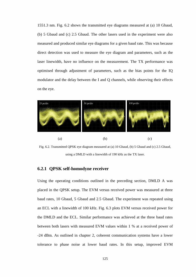
125
1551.3 nm. Fig. 6.2 shows the transmitted eye diagrams measured at (a) 10 Gbaud,
(b) 5 Gbaud and (c) 2.5 Gbaud. The other lasers used in the experiment were also
measured and produced similar eye diagrams for a given baud rate. This was because
direct detection was used to measure the eye diagram and parameters, such as the
laser linewidth, have no influence on the measurement. The TX performance was
optimised through adjustment of parameters, such as the bias points for the IQ
modulator and the delay between the I and Q channels, while observing their effects
on the eye.
(a) (b) (c)
Fig. 6.2. Transmitted QPSK eye diagram measured at (a) 10 Gbaud, (b) 5 Gbaud and (c) 2.5 Gbaud,
using a DMLD with a linewidth of 190 kHz as the TX laser.
6.2.1 QPSK self-homodyne receiver
Using the operating conditions outlined in the preceding section, DMLD A was
placed in the QPSK setup. The EVM versus received power was measured at three
baud rates, 10 Gbaud, 5 Gbaud and 2.5 Gbaud. The experiment was repeated using
an ECL with a linewidth of 100 kHz. Fig. 6.3 plots EVM versus received power for
the DMLD and the ECL. Similar performance was achieved at the three baud rates
between both lasers with measured EVM values within 1 % at a received power of
-24 dBm. As outlined in chapter 2, coherent communication systems have a lower
tolerance to phase noise at lower baud rates. In this setup, improved EVM
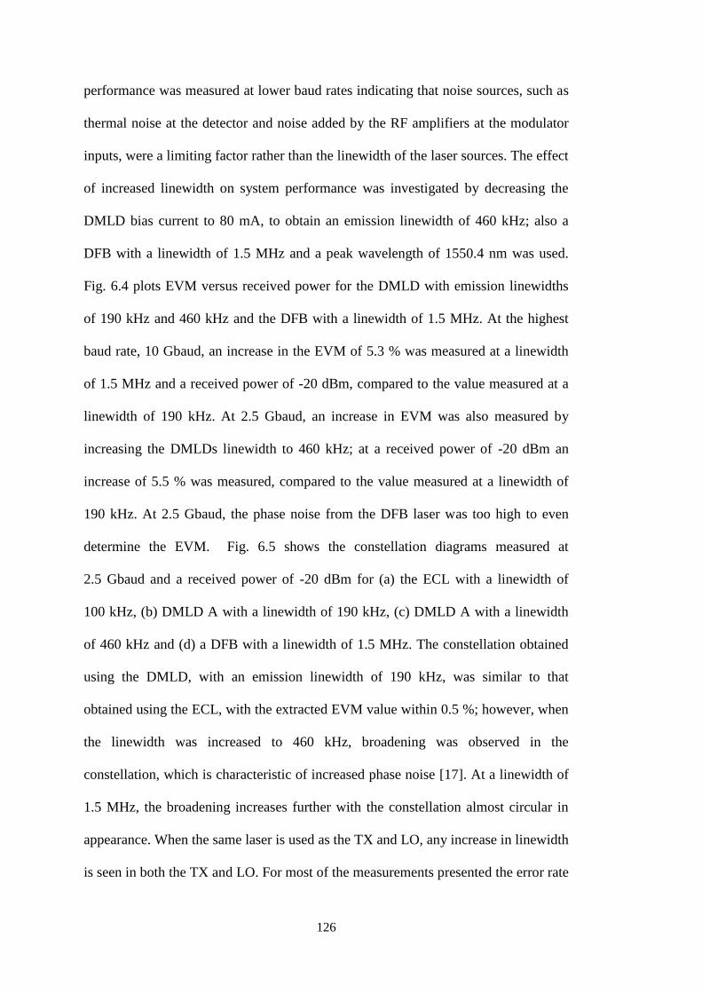
126
performance was measured at lower baud rates indicating that noise sources, such as
thermal noise at the detector and noise added by the RF amplifiers at the modulator
inputs, were a limiting factor rather than the linewidth of the laser sources. The effect
of increased linewidth on system performance was investigated by decreasing the
DMLD bias current to 80 mA, to obtain an emission linewidth of 460 kHz; also a
DFB with a linewidth of 1.5 MHz and a peak wavelength of 1550.4 nm was used.
Fig. 6.4 plots EVM versus received power for the DMLD with emission linewidths
of 190 kHz and 460 kHz and the DFB with a linewidth of 1.5 MHz. At the highest
baud rate, 10 Gbaud, an increase in the EVM of 5.3 % was measured at a linewidth
of 1.5 MHz and a received power of -20 dBm, compared to the value measured at a
linewidth of 190 kHz. At 2.5 Gbaud, an increase in EVM was also measured by
increasing the DMLDs linewidth to 460 kHz; at a received power of -20 dBm an
increase of 5.5 % was measured, compared to the value measured at a linewidth of
190 kHz. At 2.5 Gbaud, the phase noise from the DFB laser was too high to even
determine the EVM. Fig. 6.5 shows the constellation diagrams measured at
2.5 Gbaud and a received power of -20 dBm for (a) the ECL with a linewidth of
100 kHz, (b) DMLD A with a linewidth of 190 kHz, (c) DMLD A with a linewidth
of 460 kHz and (d) a DFB with a linewidth of 1.5 MHz. The constellation obtained
using the DMLD, with an emission linewidth of 190 kHz, was similar to that
obtained using the ECL, with the extracted EVM value within 0.5 %; however, when
the linewidth was increased to 460 kHz, broadening was observed in the
constellation, which is characteristic of increased phase noise [17]. At a linewidth of
1.5 MHz, the broadening increases further with the constellation almost circular in
appearance. When the same laser is used as the TX and LO, any increase in linewidth
is seen in both the TX and LO. For most of the measurements presented the error rate

127
was low, with no errors being counted. While it is not possible to obtain a BER
value, we can say that it was less than the FEC threshold of 3.8 × 10⁻³
at a received
power of -24 dBm. The only exception was at 2.5 Gbaud and a linewidth of
1.5 MHz, where a BER worse than 10-1
was calculated. Simulated values for BER
versus EVM were presented in [15], and it was shown that an EVM of approximately
32 % was required to achieve a BER of 10-3
. In all the measurements taken using the
DMLD and the ECL, EVMs below 32 % were obtained, at received power levels
greater than -32 dBm. An EVM of 15.3 % was measured at 2.5 Gbaud, at a received
power of -24 dBm using a DMLD with a linewidth of 190 kHz, based on the
simulated results this would correspond to a BER of approximately 10-10
.
Fig. 6.3. EVM versus received power measured with the QPSK setup using a self-homodyne receiver
at 10 Gbaud, 5 Gbaud and 2.5 Gbaud, for a DMLD with a linewidth of 190 kHz and an ECL with a
linewidth of 100 kHz.
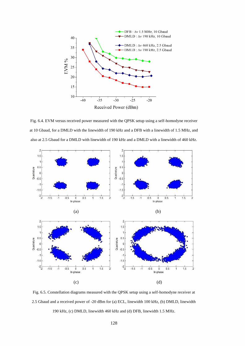
128
Fig. 6.4. EVM versus received power measured with the QPSK setup using a self-homodyne receiver
at 10 Gbaud, for a DMLD with the linewidth of 190 kHz and a DFB with a linewidth of 1.5 MHz, and
also at 2.5 Gbaud for a DMLD with linewidth of 190 kHz and a DMLD with a linewidth of 460 kHz.
(a) (b)
(c) (d)
Fig. 6.5. Constellation diagrams measured with the QPSK setup using a self-homodyne receiver at
2.5 Gbaud and a received power of -20 dBm for (a) ECL, linewidth 100 kHz, (b) DMLD, linewidth
190 kHz, (c) DMLD, linewidth 460 kHz and (d) DFB, linewidth 1.5 MHz.
129
6.2.2 QPSK heterodyne receiver
Using a heterodyne receiver setup, DMLD A was used as the TX laser and a second
DMLD, DMLD B, was used as the LO laser. DMLD B had an active region
consisting of five quantum wells, a cavity length of 2000 μm and front and back
facet reflectivities of 30 % and 95 %, respectively. The device was packaged in a
butterfly module with internal TEC, which was used to control the chip temperature.
The laser temperatures were set to 25 ˚C and 36.7 ˚C for DMLD A and DMLD B,
respectively. The peak wavelength of DMLD B was tuned via the chip temperature,
so that it matched the wavelength of the received signal. Both lasers were operated at
a bias current of 200 mA. The emission linewidths were 190 kHz and 120 kHz for
DMLD A and DMLD B, respectively, and a peak wavelength of 1551.3 nm was
measured for both. Fig. 6.6 plots EVM versus received power measured at 10 Gbaud,
5 Gbaud and 2.5 Gbaud. For comparison, the values measured using the ECL in the
self-homodyne receiver setup are also plotted. This was equivalent to using TX and
LO lasers with linewidths of 100 kHz. Similar performance was achieved using the
DMLDs in the heterodyne and an ECL in the self-homodyne receiver setup at the
three baud rates, with measured EVM values within 0.5 % at a received power of
-24 dBm. This demonstrates that narrow linewidth DMLDs can achieve similar
performance to an ECL at baud rates as low as 2.5 Gbaud, and can be used as both
TX and LO lasers in a QPSK system. Fig. 6.7 shows the constellation diagrams
measured using the heterodyne receiver setup at a received power of -20 dBm at
(a) 10 Gbaud, (b) 5 Gbaud and (c) 2.5 Gbaud.

130
Fig. 6.6. EVM versus received power measured with the QPSK setup using a heterodyne receiver at
10 Gbaud, 5 Gbaud and 2.5 Gbaud, for DMLDs as the TX and LO lasers with linewidths of 190 kHz
and 120 kHz, respectively. Also plotted an ECL with a linewidth of 100 kHz measured with a self-
homodyne receiver setup.
The improvement in performance at lower baud rates shows that the performance
was not limited by the linewidth, but rather the performance at higher baud rates was
limited by additional noise sources in the setup, such as thermal noise at the detector
and noise added by the RF amplifiers at the modulator inputs. It was not possible to
calculate a BER value as no errors were counted in the captured data; however, we
can say that the BER was better than 10-3
in all cases, at a received power of
-24 dBm. At a received power of -24 dBm the EVM values measured using the
heterodyne setup at 10 Gbaud and 2.5 Gbaud, where 23 % and 14.9 %, respectively.
Based on the simulations of EVM versus BER presented in [15], these EVM values
correspond to BERs of approximately 10-5
and 10-10
at 10 Gbaud and 2.5 Gbaud,
respectively. While some degradation in performance was observed at 10 Gbaud,
which is primarily due to intensity noise in the setup, the BER obtained at 10 Gbaud
still exceeds the FEC threshold.
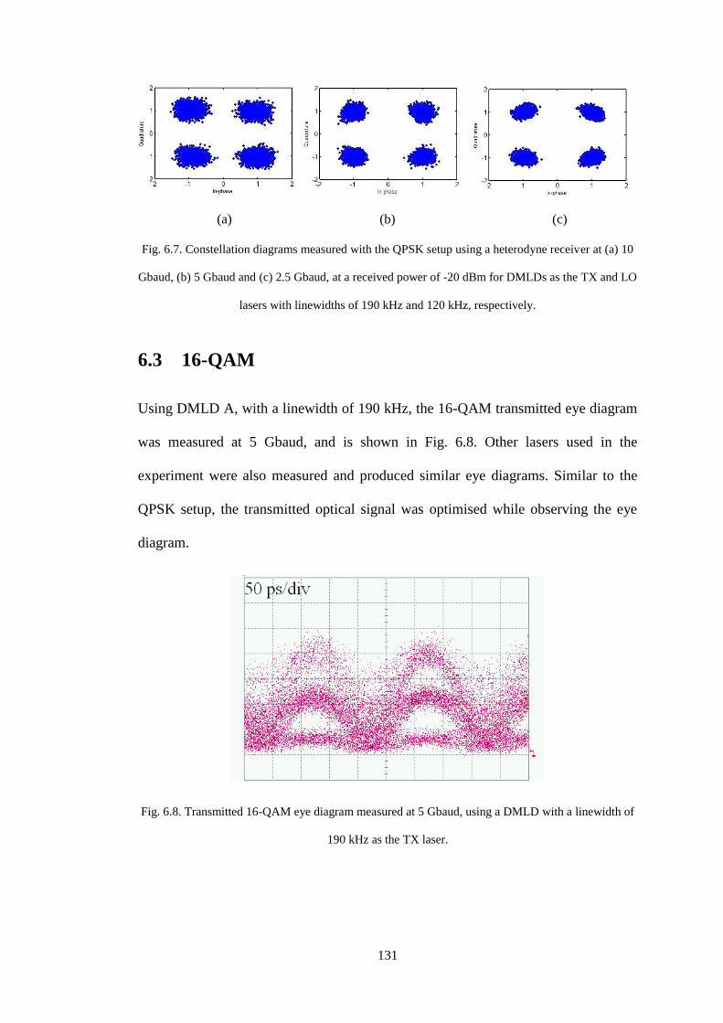
131
(a) (b) (c)
Fig. 6.7. Constellation diagrams measured with the QPSK setup using a heterodyne receiver at (a) 10
Gbaud, (b) 5 Gbaud and (c) 2.5 Gbaud, at a received power of -20 dBm for DMLDs as the TX and LO
lasers with linewidths of 190 kHz and 120 kHz, respectively.
6.3 16-QAM
Using DMLD A, with a linewidth of 190 kHz, the 16-QAM transmitted eye diagram
was measured at 5 Gbaud, and is shown in Fig. 6.8. Other lasers used in the
experiment were also measured and produced similar eye diagrams. Similar to the
QPSK setup, the transmitted optical signal was optimised while observing the eye
diagram.
Fig. 6.8. Transmitted 16-QAM eye diagram measured at 5 Gbaud, using a DMLD with a linewidth of
190 kHz as the TX laser.
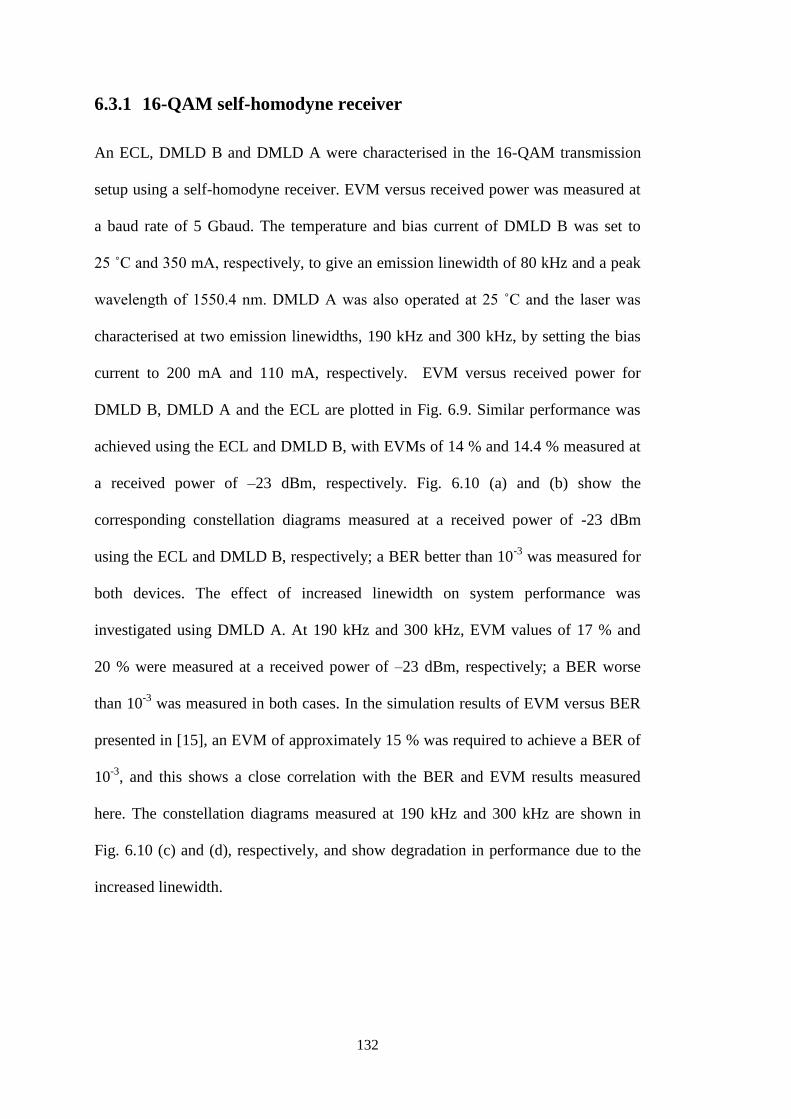
132
6.3.1 16-QAM self-homodyne receiver
An ECL, DMLD B and DMLD A were characterised in the 16-QAM transmission
setup using a self-homodyne receiver. EVM versus received power was measured at
a baud rate of 5 Gbaud. The temperature and bias current of DMLD B was set to
25 ˚C and 350 mA, respectively, to give an emission linewidth of 80 kHz and a peak
wavelength of 1550.4 nm. DMLD A was also operated at 25 ˚C and the laser was
characterised at two emission linewidths, 190 kHz and 300 kHz, by setting the bias
current to 200 mA and 110 mA, respectively. EVM versus received power for
DMLD B, DMLD A and the ECL are plotted in Fig. 6.9. Similar performance was
achieved using the ECL and DMLD B, with EVMs of 14 % and 14.4 % measured at
a received power of –23 dBm, respectively. Fig. 6.10 (a) and (b) show the
corresponding constellation diagrams measured at a received power of -23 dBm
using the ECL and DMLD B, respectively; a BER better than 10-3
was measured for
both devices. The effect of increased linewidth on system performance was
investigated using DMLD A. At 190 kHz and 300 kHz, EVM values of 17 % and
20 % were measured at a received power of –23 dBm, respectively; a BER worse
than 10-3
was measured in both cases. In the simulation results of EVM versus BER
presented in [15], an EVM of approximately 15 % was required to achieve a BER of
10-3
, and this shows a close correlation with the BER and EVM results measured
here. The constellation diagrams measured at 190 kHz and 300 kHz are shown in
Fig. 6.10 (c) and (d), respectively, and show degradation in performance due to the
increased linewidth.

133
Fig. 6.9. EVM versus received power measured with the 16-QAM setup using a self-homodyne
receiver at 5 Gbaud, for an ECL with a linewidth of 100 kHz, a DMLD with a linewidth of 80 kHz, a
DMLD with a linewidth of 190 kHz and a DMLD with a linewidth of 300 kHz.
(a) (b)
(c) (d)
Fig. 6.10. Constellation diagrams measured with the 16-QAM setup using a self-homodyne receiver at
5 Gbaud and a received power of -23 dBm for (a) ECL, linewidth 100 kHz, (b) DMLD, linewidth 80
kHz, (c) DMLD, linewidth 190 kHz and (d) DMLD, linewidth 300 kHz.

134
In comparison to the QPSK setup, where similar performance was demonstrated at
baud rates as low as 2.5 Gbaud for linewidths of 190 kHz and 100 kHz, the
degradation in performance observed using the 16-QAM setup confirms that higher
order modulation formats have more stringent linewidth requirements.
6.3.2 16-QAM heterodyne receiver
The lasers were also characterised using a heterodyne receiver setup. Fig. 6.11 plots
the EVM versus received power for three cases, first using DMLD A with a
linewidth of 190 kHz as the TX laser and DMLD B with a linewidth of 85 kHz as the
LO, second using DMLD A with a linewidth of 190 kHz as the TX laser and an ECL
with a linewidth of 100 kHz as the LO, and third using DMLD B with a linewidth of
80 kHz as the TX laser and an ECL with a linewidth of 100 kHz as the LO. The
DMLD operating conditions were as follows: the temperature and bias current of
DMLD A was set to 25 ˚C and 200 mA, respectively. When used as the LO the
temperature and bias current of DMLD B was set to 34 ˚C and 350 mA, respectively,
and when used as the TX the temperature and bias current was set to 25 ˚C and
350 mA, respectively. When used as the LO the temperature of DMLD B was used
to tune the wavelength to match that of the received signal. The performance
achieved in the first and second case was similar, with EVM values of 15.4 % and
15.1 % measured at a received power of -23 dBm, respectively. In the third case an
EVM of 14 % was measured at a received power of -23 dBm. The constellation
diagrams for the three cases measured at a received power of -23 dBm are shown in
Fig. 6.12 (a), (b) and (c), respectively. Because the error rate was higher it was
possible to estimate the error rate, in the first and second case a BER slightly worse
that 10-3
was measured. In the third case the combined linewidth was 180 kHz,
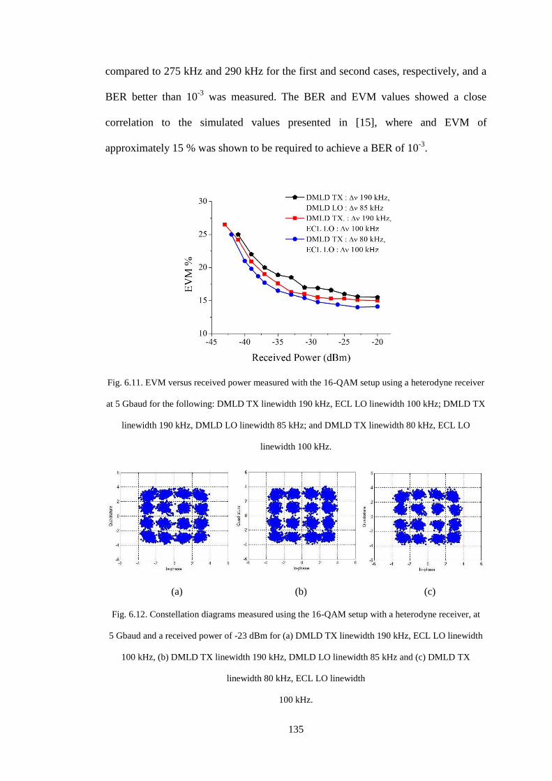
135
compared to 275 kHz and 290 kHz for the first and second cases, respectively, and a
BER better than 10-3
was measured. The BER and EVM values showed a close
correlation to the simulated values presented in [15], where and EVM of
approximately 15 % was shown to be required to achieve a BER of 10-3
.
Fig. 6.11. EVM versus received power measured with the 16-QAM setup using a heterodyne receiver
at 5 Gbaud for the following: DMLD TX linewidth 190 kHz, ECL LO linewidth 100 kHz; DMLD TX
linewidth 190 kHz, DMLD LO linewidth 85 kHz; and DMLD TX linewidth 80 kHz, ECL LO
linewidth 100 kHz.
(a) (b) (c)
Fig. 6.12. Constellation diagrams measured using the 16-QAM setup with a heterodyne receiver, at
5 Gbaud and a received power of -23 dBm for (a) DMLD TX linewidth 190 kHz, ECL LO linewidth
100 kHz, (b) DMLD TX linewidth 190 kHz, DMLD LO linewidth 85 kHz and (c) DMLD TX
linewidth 80 kHz, ECL LO linewidth
100 kHz.

136
6.4 Discussion
Characterisation results on low linewidth DMLDs were presented in chapter 4,
demonstrating linewidths as low as 70 kHz. In optical coherent communication
systems the linewidth is an important parameter, as the performance of phase
modulated signals can be limited if the phase noise of the laser sources is too high.
The level of phase noise that is tolerable depends on a number of factors, including,
the order of the modulation format used, the baud rate, the architecture of the
receiver and the DSP algorithms used. The objective of these experiments was to
compare the performance of different lasers in a coherent transmission test bed, and
to confirm that low linewidth DMLDs could achieve performance levels comparable
to an ECL.
In these experiments the main figure of merit used was the EVM. The EVM is a
standard metric used in wireless and wireline communications and it is increasingly
being used to assess the quality of optical signals employing advanced modulation
formats, with the latest optical test instruments, designed for analysing phase
modulated signals, incorporating EVM analysis tools [18]. In [15] it was
demonstrated that good agreement could be obtained between simulated values of
EVM versus BER and values obtained experimentally using six different modulation
formats, B/Q/8PSK and 16/32/64 QAM, at symbol rates of 20 Gbaud and 25 Gbaud.
While the ultimate system performance measurement is the BER, the EVM presents
a powerful tool for analysing the performance of phase modulated systems.
In the transmission setup using a self-homodyne receiver, EVM values within 1 % of
those obtained using an ECL were demonstrated. This was achieved in the QPSK
setup using a DMLD with a linewidth of 190 kHz, and in the 16-QAM setup using a

137
DMLD with a linewidth of 80 kHz. The effect of increased linewidth was also
investigated using the self-homodyne receiver setup. In the QPSK setup an increase
in EVM of approximately 5.5 % was measured at both 10 Gbaud and 2.5 Gbaud for
linewidths of 1.5 MHz and 460 kHz, respectively, compared to the values obtained at
a linewidth of 190 kHz. In the 16-QAM setup an increase in EVM of approximately
3 % and 6 % was measured at 5 Gbaud for linewidths of 190 kHz and 300 kHz,
respectively, compared to the values obtained at a linewidth of 100 kHz. These
measurements confirm that lower baud rates and higher order modulation formats
require lasers with lower linewidths. Using more advanced DSP, where feedforward
algorithms are used, it is possible to achieve greater tolerance to laser phase noise,
allowing lasers with higher linewidths to be used in these systems, potentially a
linewidth of 200 kHz could support higher order modulation formats up to 64 QAM
at 10 Gbaud [13].
Experiments were also carried using a heterodyne receiver setup, which
demonstrated that DMLDs could be used as TX and LO lasers in a coherent
communications setup. The measurements taken using the ECL with a self-
homodyne receiver setup were used as a benchmark; EVM values within 0.5 % were
measured in the QPSK setup, at the three baud rates, using DMLDs as the TX and
LO with a combined linewidth of 310 kHz. EVM values were also measured using
the 16-QAM setup, where DMLDs with a combined linewidth of 275 kHz were used
at the TX and LO; because of the higher combined linewidth, compared to the self-
homodyne case using the ECL, an increase in the EVM of 1.4 % was measured. This
was still a relatively small increase and demonstrates that similar performance can be
achieved using DMLDs in a heterodyne setup. To investigate whether the observed
increase was a limitation of the heterodyne setup used, a DMLD and ECL with a

138
combined linewidth of 180 kHz were placed in the setup, and an EVM of 14 % was
measured, which was the same value measured using the ECL in the self-homodyne
setup. Ideally two DMLDs with a linewidth of 100 kHz, or less, would have been
used in the heterodyne experiment, but only one such device was available at the
time this work was carried out.
For the QPSK measurements carried out on the DMLD and the ECL the error rate
was low, with no errors being counted in 105 acquired bits. Also, using simulated
results of BER versus EVM presented in [15] to estimate the BER, values better than
10-5
are estimated for all the measurements taken using DMLDs or the ECL. The
improved performance demonstrated at lower baud rates with lower EVM values
being measured, indicates that noise sources, such as thermal noise at the detector
and noise added by the RF amplifiers at the modulator inputs, limited the
performance rather than the linewidth of the laser sources.
For the 16-QAM measurements it was possible to estimate the BER as the error rate
was higher. Using the self-homodyne receiver setup, a BER better than 10-3
was
obtained using both a DMLD with a linewidth of 80 kHz and an ECL. For linewidths
of 190 kHz and 100 kHz, a BER worse than 10-3
was measured. In the 16-QAM
heterodyne setup using a TX laser with a linewidth of 190 kHz, BERs worse than
10-3
, but better than 10-2
, were obtained using LOs with linewidths of 100 kHz and
85 kHz, obtained from an ECL and a DMLD, respectively. A BER better that 10-3
was achieved using a DMLD with a linewidth of 80 kHz as the TX and an ECL as
the LO. The results obtained were also consistent with simulations presented in [15],
which showed that an EVM of approximately 15 % was required to achieve a BER
of 10-3
, which exceeds the FEC threshold.
139
A limitation in this setup, which limited the BER performance, was additional noise
sources in the setup, and improved performance should be possible through
optimisation of the setup. The objective of the experiments was to compare the
performance of different lasers in a coherent transmission setup and this was
achieved as the lasers were tested under the same conditions.
In chapter 4, it was demonstrated that the wavelength of low linewidth DMLDs
could be tuned over temperature, without a significant change in the measured
linewidth value, this property was utilised in the heterodyne experiments to provide a
degree of wavelength tuneabilty at the LO.
6.5 Conclusion
Similar performance to an ECL has been demonstrated using low linewidth DMLDs
in a coherent transmission system. Table 6.2 summarises the performance achieved
using the QPSK modulation format at 10 Gbaud, 5 Gbaud and 2.5 Gbaud using both
the self-homodyne and the heterodyne receiver setups measured at a received power
of -24 dBm. Comparing the results obtained using DMLDs with those obtained using
an ECL, where the ECL was measured using the self-homodyne receiver setup, very
similar performance was obtained at the three baud rates, with measured EVM values
within 0.5 % for both receiver setups. Table 6.3 summarises the performance
achieved using the 16-QAM modulation format at 5 Gbaud using both the self-
homodyne and the heterodyne receiver setups measured at a received power of
-23 dBm. In the self-homodyne receiver setup an 80 kHz DMLD showed similar
performance to an ECL, with a measured EVM values within 0.4 % for both lasers.
In the heterodyne receiver setup where DMLDs with a combined linewidth of
275 kHz were used at both the receiver and the transmitter, similar performance to an

140
ECL was demonstrated, with a measured EVM value within 1.4 % of that obtained
using an ECL. By decreasing the combined linewidth to 180 kHz in the heterodyne
setup this produced the same EVM value as was obtained using the ECL in the
homodyne setup. Because these DMLDs have the linewidths required for use in
advanced modulation format systems and present an economic approach for the
manufacture of semiconductor lasers they are an important component to consider in
the transmitters and receivers of coherent systems. The next chapter provides a
conclusion to the thesis and discusses the potential for future work in this area.
Table. 6.2. EVM values measured using the QPSK setup at 10 Gbaud, 5 Gbaud and 2.5 Gbaud, for an
ECL and a DMLD measured using the self-homodyne receiver setup and two DMLDs measured using
the heterodyne receiver setup.
Table. 6.3. EVM values measured using the 16-QAM setup at 5 Gbaud, for an ECL and a DMLD
measured using the self-homodyne receiver setup, two DMLDs measured using the heterodyne
receiver setup and a DMLD as the TX and an ECL as the LO measured using the heterodyne receiver
setup.
References
[1] K. Roberts, M. O'Sullivan, K. T. Wu, H. Sun, A. Awadalla, D. J. Krause and C.
Laperle, “Performance of Dual-Polarization QPSK for Optical Transport Systems,”
Journal of Lightwave Technology, vol. 27, no. 16, pp. 3546-3559, Aug. 2009.
100 kHz ECL
self-homodyne receiver
190 kHz DMLD
self-homodyne receiver
DMLD (TX 190 kHz, LO 120 kHz)
heterodyne receiver
10 23.4 23.6 23
5 17.8 17.7 17.3
2.5 14.8 15.3 14.9
Baud rate
(Gbaud)
EVM %
100 kHz ECL
self-homodyne receiver
80 kHz DMLD
self-homodyne receiver
DMLD
(TX 190 kHz, LO 85 kHz)
heterodyne receiver
DMLD TX 80 kHz,
ECL LO 120 kHz
heterodyne receiver
14 14.4 15.4 14
EVM %

141
[2] K. Roberts, D. Beckett, D. Boertjes, J. Berthold and C. Laperle, “100G and beyond
with digital coherent signal processing,” IEEE Communications Magazine, vol. 48, no.
7, pp. 62-69, Jul. 2010.
[3] F. Buchali, K. Schuh, D. Rosener, E. Lach, R. Dischler, W. Idle, L. Schmalen, A.
Leven, R. P. Braun, A. Ehrhardt, C. Gerlach and L. Schurer, “512-Gb/s DP-16-QAM
field trial over 734 km installed SSMF with co-propagating 10 Gb/s NRZ neighbors
incorporating soft-FEC decoding,” in Optical Fiber Communication Conference
(OFC), Los Angeles, Mar. 2012.
[4] JDS Uniphase Corporation, “Dual parallel Mach-Zehnder modulator data sheet,”
2008. [Online]. Available:
http://www.jdsu.com/ProductLiterature/dpmzmod_ds_cc_ae.pdf.
[5] JDS Uniphase Corporation, Model H301 10 Gbit/s Optical modulator driver, data
sheet.
[6] Optoplex Corporation, “2x8 Coherent Mixer, data sheet,” 2009. [Online]. Available:
http://www.optoplex.com/download/Optoplex%20Datasheets_2x8.pdf.
[7] Teleoptix, “43 Gbit/s balanced photoreceiver with linear TIA, data sheet,” 2009.
[Online]. Available: http://www.linkra.it/images/ot/pdf/40Gb-
components/Teleoptix_DualPIN-DTLIN-v1.0.pdf.
[8] JDS Uniphase Corporation, “MAP Erbium doped fiber amplifier, data sheet,” 2011.
[Online]. Available:
http://www.jdsu.com/ProductLiterature/mapedfa_ds_lab_tm_ae.pdf.
[9] MPB Communications Inc., Bench top pre-amplifier, EFA-R35-PAR, specification
sheet, 2009.
[10] I. P. Kaminow, Optical fiber telecommunications V: B: systems and networks, Boston:
Academic Press, 2008.
[11] T. N. Huynh, F. Smyth, L. Nguyen and L. P. Barry, “Effects of phase noise of
monolithic tunable laser on coherent communication systems,” Optics Express, vol.
20, no. 26, pp. B244-B249, Nov. 2012.
[12] T. Nakagawa, M. Matsui, T. Kobayashi, K. Ishihara, R. Kudo, M. Mizoguchi and Y.
Miyamoto, “Non-data-aided wide-range frequency offset estimator for QAM optical
coherent receivers,” in Optical Fiber Communication Conference (OFC), Los Angeles,
Mar. 2011.
[13] T. Pfau, S. Hoffmann and R. Noe, “Hardware-Efficient Coherent Digital Receiver
Concept With Feedforward Carrier Recovery for M-QAM Constellations,” Journal of
Lightwave Technology, vol. 27, no. 8, pp. 989-999, April 2009.
142
[14] M. Seimetz, High-Order Modulation for Optical Fiber Transmission, Berlin: Springer,
2009.
[15] R. Schmogrow, B. Nebendahl, M. Winter, A. Josten, D. Hillerkuss, S. Koenig, J.
Meyer, M. Dreschmann, M. Huebner, C. Koos, J. Becker, W. Freude and J. Leuthold,
“Error Vector Magnitude as a Performance Measure for Advanced Modulation
Formats,” IEEE Photonics Technology Letters, vol. 24, no. 1, pp. 61-63, Jan. 2012.
[16] R. A. Shafik, S. Rahman and A. H. M. R. Islam, “On the Extended Relationships
Among EVM, BER and SNR as Performance Metrics,” in International Conference on
Electrical and Computer Engineering (ICECE), Dhaka, Dec. 2006.
[17] O. Funke and B. Nebendahl, Short Course 369, Test and measurement of complex
modulated optical signals, Los Angeles: Optical Fiber Communication Conference
(OFC), Mar. 2012.
[18] Agilent Technologies, “Agilent N4391A, Optical Modulation Analyzer, Data sheet,”
2011. [Online]. Available: http://cp.literature.agilent.com/litweb/pdf/5990-
3509EN.pdf.

143
Chapter 7
Conclusion and future work
7.1 Conclusion
The demand for optical networks with higher capacity looks set to continue, with
global IP traffic forecast to grow at a compound annual rate of 32 % up to 2015 [1].
Factors such as the availability of new services, customer demands and policy
initiatives by governments are all pushing for the delivery of higher speed broadband
connections. The delivery of higher speed connections is dependent on extending the
reach of fibre in the field and increasing the cumulative capacity of the network
infrastructure. In the access network the bit rate of next generation systems is likely
to increase to 10 Gbit/s, making high speed transmitters a requirement. The latest
systems being deployed in core and long haul applications are employing advanced
modulation formats to cope with the increase in data traffic. These modulation
formats encode the information in the phase of the optical carrier making low phase
noise a requirement for optical sources used in these systems.
In this thesis a novel type of single mode laser called a discrete mode laser was
proposed for next generation fibre optic communications applications. This approach
offers the potential for high-volume, low-cost fabrication of single-mode lasers.

144
Single-wavelength operation in DMLDs is achieved by introducing index
perturbations in the form of etched features positioned at a small number of sites
distributed along the surface of the ridge waveguide. The fabrication process does
not involve epitaxial re-growth and only requires standard optical lithography. A
significant element in the cost of producing a laser module is packaging: monolithic
semiconductor lasers, such as the DMLD and DFBs, can use existing
telecommunication laser packaging platforms to produce lasers in high volumes; this
is not easily achieved with ECLs, which have more complex packaging
requirements. Two types of laser were considered, a directly modulated transmitter
and a narrow linewidth laser and the main results are summarised here:
Direct modulation
10 Gbit/s operation was demonstrated at 1310 nm and 1550 nm using a directly
modulated DMLD. The transmission performance was also characterised, at
1310 nm after transmission through 22 km of SSMF a power penalty of only 0.3 dB
was measured. At 1550 nm a power penalty of 0.8 dB was measured after 10 km but
this increased to 5.3 dB after 20 km. A potential application area for 10 Gbit/s
1310 nm DMLDs is in access networks. However, limitations in this particular
process run meant that the operating temperature was limited. In chapter 4 a 1310 nm
DMLD demonstrated single mode operation over the range -40 ˚C ≤ T ≤ 97 ˚C, while
there were differences in the design of this device compared to the 10 Gbit/s part, it
does demonstrate that a wide operating temperature range can be achieved. The
applications of 10 Gbit/s directly modulated lasers at 1550 nm may be limited in
access networks due to dispersion effects. However, if dispersion compensation can
be cost effectively deployed directly modulated lasers would be an attractive option
for access networks because of their lower cost.
145
Narrow linewidth
In chapter 4 three variations of low linewidth DMLD designs were characterised and
all demonstrated linewidths below 200 kHz. The first device results were presented
on, displayed a minimum linewidth of 138 kHz. It also demonstrated that single
mode operation could be maintained over a wide temperature range of
-10 ˚C ≤ T ≤ 110 ˚C. The device also showed stable linewidth performance over the
temperature range 0 ˚C ≤ T ≤ 85 ˚C, where at a constant power of 4 mW a maximum
linewidth of 235 kHz was measured at 85 ˚C, and a minimum value of 212 kHz was
measured at 25 ˚C, corresponding to a variation in the linewidth of only 23 kHz over
the measured temperature range.
A second device was designed with a cavity length of 2 mm, and a minimum
linewidth of 70 kHz was demonstrated when measured using the D-SH technique.
The PSD of the laser was also measured to obtain more detailed information relating
to the phase noise and to confirm the accuracy of the results obtained using the D-SH
technique. From the PSD measurement a linewidth value of 67 kHz was extracted,
and this agrees closely with the value measured using the D-SH technique.
A third device was designed for higher output powers and low linewidth. Using this
device a linewidth below 200 kHz and an output power from the front facet in excess
of 30 mW was demonstrated.
Chapter 6 characterised the performance of these low linewidth DMLDs in a
coherent transmission test bed employing the advanced modulation formats QPSK
and 16-QAM, and the performance levels achieved were compared with that
obtained using an ECL. In the transmission setup a self-homodyne receiver was
implemented, and EVM values within 1 % of those obtained using an ECL were

146
demonstrated using DMLDs. It was also demonstrated that DMLDs could be used as
both TX and LO lasers in a heterodyne setup, and that tuning of the peak wavelength
via the laser temperature could be used to match the wavelength of the TX and LO
lasers. These were the first demonstrations where DMLDs were used as the TX or
LO in a coherent transmission setup using these modulation formats.
7.2 Future work
The DMLDs presented in this thesis show potential for deployment in future optical
systems. However, there are areas where further development will be necessary, and
avenues for future research are outlined below:
1310 nm directly modulated lasers
Further work will be required to improve the temperature performance of the
1310 nm DMLD operating at 10 Gbit/s. Based on information gained from the
previous development run, the epitaxial material appears to have the requisite
bandwidth even at 85 ˚C. A first step is to use wafers from the same epitaxial growth
and process a further DMLD development run. The steps in future development work
include achieving single mode operation over a wide temperature range, and then
assess the static and dynamic performance over the temperature range to determine
its suitability, or otherwise, for 10 Gbit/s access applications.
1550 nm directly modulated lasers
Using existing 1550 nm devices there is potential to achieve improved dynamic
performance. A first step is to package devices with a HR coated back facet and a
cavity length of 300 μm, or less, in a high speed package in order to evaluate its
performance. The applications of 10 Gbit/s, or higher speed, directly modulated

147
lasers operating at 1550 nm may be limited due to dispersion effects. However, the
development of a high speed 1550 nm structure will also be required for on-going
work in areas such as optical comb sources [2, 3] and monolithic integration of dual
section devices, where improved performance can be achieved through optical
injection [4].
Narrow linewidth lasers
The linewidth of DMLDs could be further reduced by increasing the cavity length
beyond 2 mm. However, handling and packaging such a device becomes more
difficult. Reducing the linewidth further is a focus for on-going research, and areas
such as the material structure and using higher reflectivity on the front facet are
being investigated. The development of a narrow linewidth device capable of full C
or L-band tuneability could be implemented using an array of DMLDs. Each laser in
the array is designed to cover a number of channels and course tuning of the
wavelength is achieved by selecting a laser in the array and fine tuning is
accomplished by adjusting the laser temperature. As demonstrated previously narrow
linewidth DMLDs can achieve a wide temperature tuning range, and this would be a
desirable characteristic in such a device. This approach has previously been used
with DFBs, in [5] full C-band tuneability was demonstrated using an array of 12
DFBs and a micro-electro-mechanical system (MEMs) incorporated in an optical
package. Light from the selected laser in the array is coupled to the output fibre by
tilting a MEMs mirror. An alternative approach was used in [6] to produce an
integrated chip, consisting of an array of 12 DFBs, an MMI and a semiconductor
optical amplifier (SOA). Light from the laser array is coupled using the MMI and the
SOA is used to control the output power.

148
References
[1] Cisco systems Inc., White paper, “Cisco Visual Networking Index: Forecast and
Methodology, 2010–2015,” 1 June 2011. [Online]. Available:
http://www.cisco.com/en/US/solutions/collateral/ns341/ns525/ns537/ns705/ns827/whi
te_paper_c11-481360.pdf.
[2] P. M. Anandarajah, R. Maher, Y. Q. Xu, S. Latkowski, J. O'Carroll, S. G. Murdoch, R.
Phelan, J. O'Gorman and L. P. Barry, “Generation of Coherent Multicarrier Signals by
Gain Switching of Discrete Mode Lasers,” IEEE Photonics Journal, vol. 3, no. 1, pp.
112-122, Feb. 2011.
[3] R. Zhou, S. Latkowski, J. O'Carroll, R. Phelan, L. P. Barry and P. Anandarajah, “40nm
wavelength tunable gain-switched optical comb source,” in European Conference and
Exhibition on Optical Communication (ECOC), Geneva, Sept. 2011.
[4] C. Browning, K. Shi, S. Latkowski, P. Anandarajah, F. Smyth, B. Cardiff, R. Phelan
and L. P. Barry, “Performance improvement of 10Gb/s direct modulation OFDM by
optical injection using monolithically integrated discrete mode lasers,” in European
Conference and Exhibition on Optical Communication (ECOC), Geneva, Sept. 2011.
[5] B. Pezeshki, E. Vail, J. Kubicky, G. Yoffe, S. Zou, J. Heanue, P. Epp, S. Rishton, D.
Ton, B. Faraji, M. Emanuel, X. Hong, M. Sherback, V. Agrawal, C. Chipman and T.
Razazan, “20-mW widely tunable laser module using DFB array and MEMS
selection,” IEEE Photonics Technology Letters, vol. 14, no. 10, pp. 1457-1459, Oct.
2002.
[6] H. Ishii, K. Kasaya and H. Oohashi, “Reduced spectral linewidth (≪ 0.6 MHz) in L-
band wavelength tunable DFB laser array,” in IEEE International Semiconductor
Laser Conference, Sorrento, Sept. 2008.

149
Appendix A
List of Publications Arising From This
Work
A.1 Referred Journals
1. O’Carroll, J.; Phelan, R.; Kelly, B; Huynh, T.N.; Cardiff, B.; Smyth, F;
Anandarajah, P.M.; and Barry, L.P. "Narrow-Linewidth Discrete-Mode Laser
Diodes for Coherent Communication Applications"; Journal of Optical
Communications and Networking, Vol. 4, Issue 9, pp.: A90-A96 (2012)
2. Anandarajah, P.M.; Latkowski, S.; Browning, C.; Zhou, R.; O'Carroll, J.;
Phelan, R.; Kelly, B.; O'Gorman, J.; Barry, L.P.; “Integrated Two-Section
Discrete Mode Laser”; Photonics Journal, IEEE, Vol. 4, Issue 6, pp.: 2085-
2094 (2012).
3. Phelan, R.; O'Carroll, J.; Byrne, D. ; Herbert, C. ; Somers, J. ; Kelly, B.;
“In0.75Ga0.25As/InP Multiple Quantum Well Discrete Mode Laser Diode
Emitting at 2 um”; Photonics Technology Letters, IEEE, Vol. 24, Issue 8, pp.:
652 – 654 (2012).
4. O’Carroll, J.; Phelan, R.; Kelly, B.; Byrne, D.; Barry, L.P.; O’Gorman, J.;
“Wide temperature range 0 < T < 85 °C narrow linewidth discrete mode laser
diodes for coherent communications applications”; Optics Express, Vol. 19
Issue 26, pp.B90-B95 (2011).
5. Zhou, R.; Latkowski, S.; O’Carroll, J.; Phelan, R.; Barry, L.P.; Anandarajah,
P.; “40nm wavelength tunable gain-switched optical comb source”; Optics
Express, Vol. 19 Issue 26, pp.B415-B420 (2011).
6. Weerasuriya, R.; Sygletos, S.; Ibrahim, S.K.; Gunning, F.C.G.; Manning,
R.J.; Phelan, R.; O'Carroll, J.; Kelly, B.; O'Gorman, J.; Ellis, A.D.;
“Comparison of Frequency Symmetric Signal Generation From a BPSK Input

150
Using Fiber and Semiconductor-Based Nonlinear Elements”; Photonics
Technology Letters, IEEE, Vol. 23 Issue:10, pp.: 651 – 653 (2011).
7. O'Brien, S.; Smyth, F.; Kai Shi ; O'Carroll, J.; Anandarajah, P.M.; Bitauld,
D.; Osborne, S.; Phelan, R.; Kelly, B.; O'Gorman, J.; Peters, F.H.; Roycroft,
B.; Corbett, B.; Barry, L.P.; “Design, Characterization, and Applications of
Index-Patterned Fabry–Pérot Lasers”; IEEE Journal of Selected Topics in
Quantum Electronics, Vol. 17, Issue 6, pp.: 1621–1631 (2011).
8. Anandarajah, P.M.; Maher, R.; Xu, Y.Q.; Latkowski, S.; O'Carroll, J.;
Murdoch, S.G.; Phelan, R.; O'Gorman, J.; Barry, L.P.; “Generation of
Coherent Multicarrier Signals by Gain Switching of Discrete Mode Lasers”;
Photonics Journal, IEEE, Vol. 3, Issue 1, pp.: 112–122 (2011).
9. Phelan, R.; Slight, T.J.; Kelly, B.; O'Carroll, J.; McKee, A.; Revin, D.G.;
Zhang, S.Y.; Krysa, A.B.; Kennedy, K.L.; Cockburn, J.W.; Ironside, C.N.;
Meredith, W.; O'Gorman, J.; “Room-Temperature Operation of Discrete-
Mode InGaAs–AlAsSb Quantum-Cascade Laser With Emission at λ =3.3
um”; Photonics Technology Letters, IEEE, Vol. 22 Issue 17, pp.: 1273–1275
(2010)
10. Maher, R.; Shi, K.; Barry, L.P.; O’Carroll, J.; Kelly, B; Phelan, R;
O’Gorman, J; Anandarajah, P.M.; “Implementation of a cost-effective optical
comb source in a WDM-PON with 10.7Gb/s data to each ONU and 50km
reach”; Optics Express, Vol. 18 Issue 15, pp.15672-15681 (2010).
11. Herbert, C.; Jones, D.; Kaszubowska-Anandarajah, A.; Kelly, B.; Rensing,
M.; O'Carroll, J.; Phelan, R.; Anandarajah, P.; Perry, P.; Barry, L.P.;
O'Gorman, J.; “Discrete mode lasers for communication applications”;
Optoelectronics, IET, Vol. 3 Issue 1, pp.: 1–17 (2009).
12. Phelan, R.; Kelly, B.; O'Carroll, J.; Herbert, C.; Duke, A.; O'Gorman, J.; “-
40 °C < T < 95 °C mode-hop free operation of an uncooled AlGaInAs-MQW
discrete-mode laser diode with emission at λ = 1.3 μm.”; Electronics Letters,
Vol.: 45 Issue 1, pp.: 43–45 (2009).
13. Anandarajah, P.M.; Shi, K.; O’Carroll, J.; Kaszubowska, A.; Phelan, R.;
Barry, L.P.; Ellis, A.D.; Perry, P.; Reid, D.; Kelly, B.; O’Gorman, J.; “Phase

151
shift keyed systems based on a gain switched laser transmitter”; Optics
Express, Vol. 17 Issue 15, pp.12668-12677 (2009).
152
A.2 Conference Papers
1. Phelan, R.; O'Carroll, J.; Byrne, D. ; Herbert, C. ; Somers, J. ; Kelly, B.;
“In0.75Ga0.25As/InP Multiple Quantum Well Discrete Mode Laser Diode
Emitting at 2 μm”; MIOMD-XI Infrared Optoelectronics: Materials and
Devices Conference, 4 – 8 Sept. 2012
2. MacSuibhne, N.; Li, Z; Baeuerle, B.; Zhao, J.; Wooler, J.P.; Alam, S.U.;
Poletti, F.; Petrovich, M.N.; Heidt, A.M.; Giles, I.P.; Giles, D.J.; Pálsdóttir,
B.; Grüner-Nielsen, L.; Phelan, R.; O’Carroll, J.; Kelly, B.; Murphy, D.;
Ellis, A.D.; Richardson, D.J.; Garcia Gunning, F.C.; “Wavelength Division
Multiplexing at 2µm”; Postdeadline paper, European Conference and
Exhibition on Optical Communication (ECOC), 16 – 20 Sept. 2012
3. Huynh, T.N.; O'Carroll, J.; Smyth, F.; Shi, K.; Nguyen, L.; Anandarajah, P.;
Phelan, R.; Kelly, B.; Barry, L.P.; “Low linewidth lasers for enabling high
capacity optical communication systems”; International Conference on
Transparent Optical Networks (ICTON), 2 – 5 July 2012.
4. O’Carroll, J.; Phelan, R; Kelly, B; Byrne, D; Smyth, F; Cardiff, B;
Anandarajah, P.M.; Barry L.P.; “Narrow linewidth discrete mode laser diodes
at 1550 nm”; Paper 8432-25 of Conference 8432, Spie Photonics Europe 16 –
19 April 2012.
5. O'Carroll, J; Phelan, R; Kelly, B; Byrne, D; Anandarajah, P.M.; Latkowski,
S.; Barry, L.P.; “Discrete mode laser diodes for FTTH/PON applications up
to 10 Gbit/s”; Paper 8432-71 of Conference 8432, Spie Photonics Europe 16
– 19 April 2012.
6. O'Carroll, J; Phelan, R; Kelly, B; Byrne, D; Smyth, F; Cardiff, B;
Anandarajah, P.M.; Barry L.P.; “Narrow Linewidth Discrete Mode Laser
Diodes for Advanced Modulation Formats”; paper OTu1G.4, Optical Fiber
Communication Conference and Exposition and The National Fiber Optic
Engineers Conference (OFC/NFOEC), 4 – 8 March 2012.
7. O'Carroll, J.; Phelan, R.; Kelly, B.; Byrne, D.; Barry, L.P.; O'Gorman, J.;
“Wide temperature range 0 < T < 85 °C narrow linewidth discrete mode laser
diodes for coherent communications applications”; European Conference and
Exhibition on Optical Communication (ECOC), 18 – 22 Sept. 2011
153
8. O'Carroll, J; Phelan, R; Kelly, B; Byrne, D; Anandarajah, P.M.; Latkowski,
S.; Barry, L.P.; O’Gorman, J.; “Uncooled Discrete Mode Laser Diodes for
FTTH/PON Applications up to 10 Gbit/s”; Photonics Ireland conference, 7 –
9 September 2011.
9. Zhou R.; Latkowski, S.; O'Carroll, J.; Phelan, R.; Barry, L.P.; Anandarajah,
P.; “40nm wavelength tunable gain-switched optical comb source”; European
Conference and Exhibition on Optical Communication (ECOC), 18 – 22
Sept. 2011.
10. Fragkos, A.; Bogris, A.; Syvridis, D.; Phelan, R.; O'Carroll, J.; Kelly, B.;
O'Gorman, J.; “Amplitude regeneration of phase encoded signals using
injection locking in semiconductor lasers”; Optical Fiber Communication
Conference and Exposition and The National Fiber Optic Engineers
Conference (OFC/NFOEC), 6 – 10 March 2011.
11. Gruet, F.; Bandi, T.; Mileti, G.; Phelan, R.; O'Carroll, J.; Kelly, B.;
O'Gorman, J.; “Development and spectral characterisation of discrete mode
laser diodes (DMLDs) emitting at 780 nm for Rubidium atomic clocks”;
European Conference on Lasers and Electro-Optics and the International
Quantum Electronics Conference, 22 – 26 May 2011
12. Weerasuriya, R.; Sygletos, S.; Ibrahim, S.K.; Phelan, R.; O'Carroll, J.;
Kelly, B.; O'Gorman, J.; Ellis, A.D.; “Generation of frequency symmetric
signals from a BPSK input for phase sensitive amplification”; Optical Fiber
Communication Conference and Exposition and The National Fiber Optic
Engineers Conference (OFC/NFOEC), 21-25 March 2010.
13. Sygletos, S.; Weerasutiya, R.; Ibrahim, S.; Gunning, F.; Ellis, A.; Phelan, R.;
O'Gorman, J.; O'Carroll, J.; Kelly, B.; “A novel method of pump and idler
signal generation for non-degenerate FWM based phase sensitive
amplification”; European Conference on Lasers and Electro-Optics and the
International Quantum Electronics Conference, 16-21 May 2010.
14. Anandarajah, P.M.; Barry, L.P.; Kaszubowska, A.; O'Gorman, J.; O'Carroll,
J.; Herbert, C.; Phelan, R.; Duke, A.S.; “Highly coherent picosecond pulse
generation with sub-ps jitter and high SMSR by gain switching Discrete
Mode laser diodes at 10 GHz line rate”; Optical Fiber Communication
Conference and Exposition and The National Fiber Optic Engineers
Conference (OFC/NFOEC), 22-26 March 2009.