Embed Size (px)
Citation preview

Novel Architecture of Illuminable Variable Density Two-Dimensional Electron
SystemS.Brandsen, J. Pollanen, J.P. Eisenstein
Institute for Quantum Information and Matter (IQIM), Condensed Matter Physics, Caltech
L.N. Pfeiffer, K.W. WestPrinceton Univ., Dept. of Electrical Engineering

Outline
• Two-Dimensional Electron System: Collective electron states
• Question: Phenomena as a function of charge density?
• Illuminable Variable Density Two-Dimensional Electron System: Fabrication, Magnetotransport, Future Uses

Beyond single particle physics
Can we control interactions ?
A zoo of collective electron ground states!
VH
B - fi
eld
i
Vv=5/2

Single interface
AlGaAs
GaAs
2DES d dopants
AlGaAs
Conduction Band
Valence Band
GaAs
Cleaning up with light
AlGaAs
GaAs
2DES d dopants
AlGaAs
Conduction Band
Valence Band
GaAs

Conflict between light and gating
AlGaAs
GaAs
2DES d dopantsVg

Transparent n+ layer
GaAs
AlGaAs
Si Si Sin+ GaAs d dopants2DES

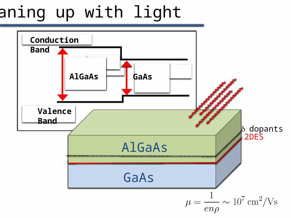
Characterization of 2DES
Etched n+ to depletion
μ2DES : 3x106 cm2/Vs, n2DES: 1.2x10¹¹ carriers/cm2
R xx (Ω
)
Field Strength (Tesla) n+
GaAs
AlGaAs

Characterization of 2DES
Diffused Ni/Au/Ge Contacts
μ2DES : 3x106 cm2/Vs, n2DES: 1.2x10¹¹ carriers/cm2
R xx (Ω
)
Field Strength (Tesla) n+
GaAs
AlGaAs
Initial Characterization
GaAs
AlGaAs
DiffusedNi/Au/Ge contacts
μ2DES : 3x106 cm2/Vs, n2DES: 1.2x10¹¹ carriers/cm2
Known values
Fit Parameters
R xx (Ω
)
Field Strength (Tesla)
μn+: 3x104 cm2/Vsnn+ : 7.4x10¹² carriers/cm2

Fabrication Procedure
n+AlGaAs
Etch away n+GaAs
AlGaAs
Si Si Sin+ GaAs d
dopants2DES
GaAs
AlGaAs

Fabrication Procedure
n+AlGaAs
Diffused Ni/Au/Ge Contacts
GaAs
AlGaAs
Si Si Sin+ GaAs d
dopants2DES
GaAs
AlGaAs
Fabrication Procedure
n+AlGaAs
Shallow Pd/Au/Ge Contacts
GaAs
AlGaAs
Si Si Sin+ GaAs d
dopants2DES
GaAs
AlGaAs

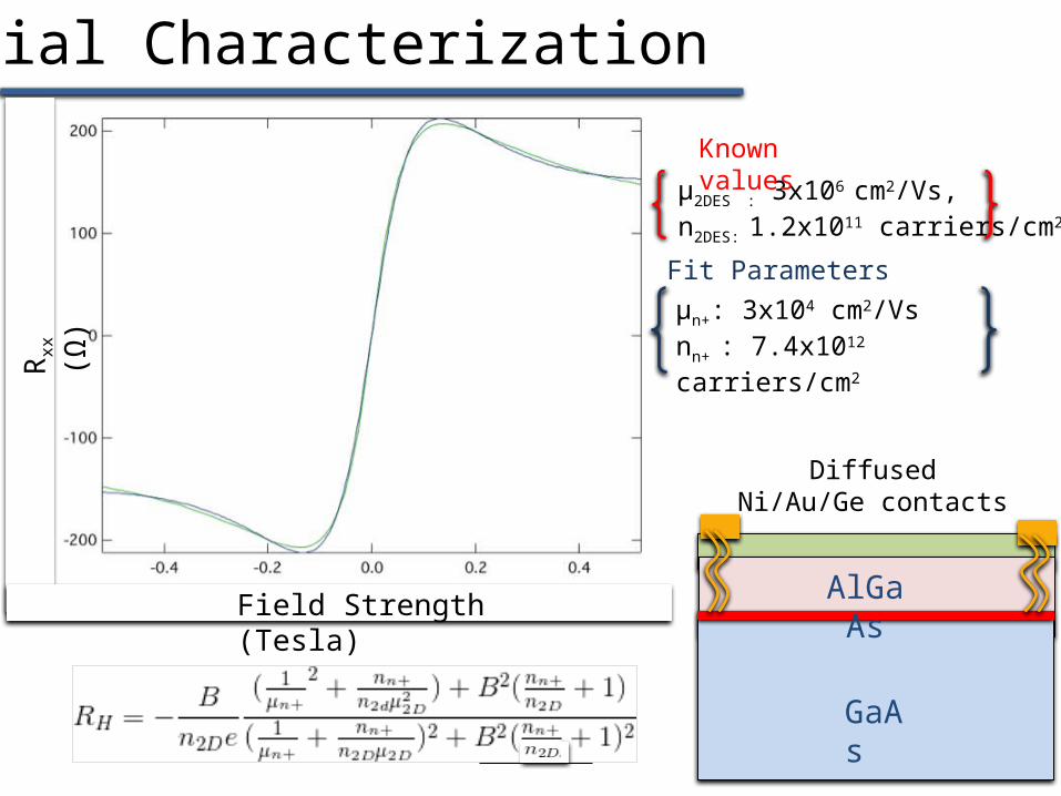
Fabrication Procedure
n+AlGaAs
Shallow Pd/Au/Ge Contacts
GaAs
AlGaAs
Si Si Sin+ GaAs d
dopants2DES
GaAs
AlGaAs

Density calibration of n+ sample
2
VH
curre
nt in
B - fi
eld
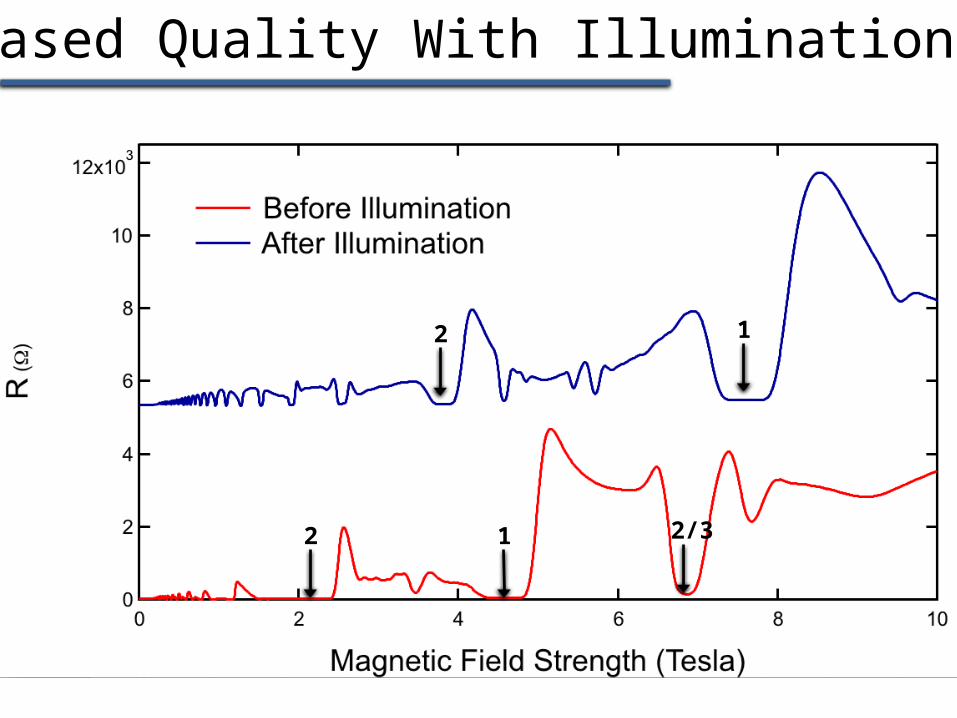
Increased Quality With Illumination
1
1
2
2
2/3

300mK magneto-transport
2
1
1
1
1
2/3
2/3
2/3
2/32
2
2
2

Mobility of 2DES versus n

Conclusions
• Development of illuminable high mobility, variable density 2DES
• Potential to explore the role of charge density in 2DES phenomena

Effective Gating After Illumination
300
0 Ω
1
12
2