Embed Size (px)
Citation preview
1 1 1 1 1
Index
Soldering point.
Male connector.
Female connector.
M/F faston connector.
Test point.
Supply voltage. Logic supply ground.
Analog supply ground.
Chassis ground.
Earth ground.
Flag joined with one or more flags
GENERALMUSIC S.p.A. Sales Division: 47842 S.Giovanni in Marignano (RN) ITALY - Via delle Rose, 12 - tel. 0541/959511 - fax 0541/957404
GENERALMUSIC on the NET: http://www.generalmusic.com
Technical Specifications, Introduction, Test Procedures & Adjustments2
Block Diagram3
Layout & Assembly AMP4, AMP8
5
6 Schematics
Layout & Assembly AMP12, Spare Part List
4
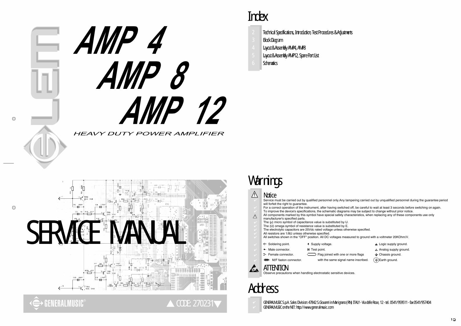
SERVICE MANUAL
CODE: 270231
Warnings
with the same signal name inscribed.
Address
ATTENTIONObserve precautions when handling electrostatic sensitive devices.
NoticeService must be carried out by qualified personnel only.Any tampering carried out by unqualified personnel during the guarantee periodwill forfeit the right to guarantee.For a correct operation of the instrument, after having switched off, be careful to wait at least 3 seconds before switching on again.To improve the device's specifications, the schematic diagrams may be subject to change without prior notice.All components marked by this symbol have special safety characteristics, when replacing any of these components use onlymanufacturer's specified parts.The (µ) micro symbol of capacitance value is substituted by U.The (Ω) omega symbol of resistance value is substituted by E. The electrolytic capacitors are 25Vdc rated voltage unless otherwise specified.All resistors are 1/8Ω unless otherwise specified.All switches shown in the "OFF" position. All DC voltages measured to ground with a voltmeter 20KOhm/V.

22222
TECHNICAL SPECIFICATIONSTECHNICAL SPECIFICATIONSTECHNICAL SPECIFICATIONSTECHNICAL SPECIFICATIONSTECHNICAL SPECIFICATIONS
Dimensions(WxHxD): AMP4 483x88x442mm (2U)
AMP8 483x88x442mm (2U)
AMP12 483x132x442mm (3U)
Weight: AMP4 12.5Kg
AMP8 15Kg
AMP12 18.5Kg
Power Requirements: (230Vac±10% 50Hz)
AMP4 540VA
AMP8 1100VA
AMP12 2000VA
Output Power EIA: (4Ω, 1KHz, 1% THD, both channels)
AMP4 2x 235Watts
AMP8 2x 424Watts
AMP12 2x 562Watts
Max. Undistorted Out: (4Ω, 1KHz, 1% THD, both channels)
AMP4 124Vpp
AMP8 164Vpp
AMP12 190Vpp
Input Sensitivity: (0dB) 0.775Vrms
Input Impedance: (balanced) 20KΩ
(unbalanced) 10KΩ
Voltage Gain: AMP4 31±0.5dB
AMP8 33±0.5dB
AMP12 35±0.5dB
Slew Rate: 20V/µS
Damping Factor: (8Ω both channels) >200
Frequency Response (20Hz÷20KHz) 0,-1dB
IMD: <0.1%
THD: (THD+N) <0.1%
S/N Ratio: >105dB
Crosstalk: (1KHz) >80dB
TEST PROCEDURES & ADJUSTMENTSTEST PROCEDURES & ADJUSTMENTSTEST PROCEDURES & ADJUSTMENTSTEST PROCEDURES & ADJUSTMENTSTEST PROCEDURES & ADJUSTMENTS
PrecautionPrecautionPrecautionPrecautionPrecaution
To prevent short circuit during any test, the oscilloscope must bethe oscilloscope must bethe oscilloscope must bethe oscilloscope must bethe oscilloscope must beEARTH insulatedEARTH insulatedEARTH insulatedEARTH insulatedEARTH insulated, this occurs because some test require to connect itsprobe to the amplifier output, noncompliance may cause damages tooscilloscope inputs circuitry.
Read these notes entirely before proceeding to any operation. Thesenotes are not comprehensive of all damages that possibly occur, butincludes some specifically advices, checks and adjustments relative tothis amplifier.
RemarksRemarksRemarksRemarksRemarks
The output circuit is an AB class amplifier with the peculiarity of transistorcollectors connected directly to chassis ground, this permit a majortemperature stability and dissipated power efficiency. The final stage isoversized to obtain high dynamic and high current with hard loads. Touse the amplifier in bridge mode the power supply is realized with two DCrails each one for its channel.
All components of channel 1 are marked by A suffix as many all compo-nents of channel 2 are marked by B suffix.
Visual CheckVisual CheckVisual CheckVisual CheckVisual Check
Use compressed air to clear dust in the amplifier chassis.
Before proceed to supply the amplifier check visually the internal assem-bly, if appears an evident damage find the most possible reasons thatcause it.
Check the wiring cables for possible interruptions or shorts.
If the damage has burnt a printed circuit board don’t try to repair it,replace with a new one.
Test InstrumentsTest InstrumentsTest InstrumentsTest InstrumentsTest Instruments
Audio Generator
Dual Trace Oscilloscope (ch.1 named as A, ch.2 as B)
Digital Multimeter
4Ω 700W, 100Ω 100W resistors
Variac (0÷250Vac)
SetupSetupSetupSetupSetup
Connect the Variac between the mains and the amplifier and set it at zerovoltage.
Set the amplifier in PARALLEL MODE and turn full clockwise the LEVELpotentiometers.
Connect the audio generator to the channel inputs and set it to 1KHz775mVRMS (0dB) sinusoidal signal.
Switch off the LIMITER from rear panel.
The procedures that follow must be executed subsequently in the orderspecified.
Supply CheckSupply CheckSupply CheckSupply CheckSupply Check
Remove the transformer secondary fuses (located on SUPPLY board),set the Variac to the nominal mains voltage, check with the Multimeterthe AC supply voltages:
AMP4: F601-F602=91±5VacAMP8: F601-F602=120±6Vac.AMP12: F601-F602=144±7Vac.
Reset the Variac at zero voltage, turn off the amplifier and put the fusesback on its holders.
Connect the oscilloscope probes A and B to the channel outputs beforeoutput relays (R151), and its ground clip to the heatsink set both to 20V/div. 200µS/div.
Set up the Variac slowly monitoring the Outputs with the oscilloscopetraces A/B, these should display the sinusoidal input signal amplified withno distortions, if a distortion occur check the POWER boards as sug-gested in the ADVICES section.
If the protection trips, turn off the amplifier, wait some minutes anddisconnect the supplies (W108 on SUPPLY board) from the channel goesin protect mode, continue to check the supplies.
Finally verify the DC supplies for each channel on SUPPLY board:AMP4:W108 pin 1-2 (+Vcc) =+62±2VdcW108 pin 3-4 (-Vcc) =-62±2VdcAMP8:W108 pin 1-2 (+Vcc) =+82±3VdcW108 pin 3-4 (-Vcc) =-82±3VdcAMP12:W108 pin 1-2 (+Vcc) =+98±4VdcW108 pin 3-4 (-Vcc) =-98±4Vdcand on MAIN board:Q130 pin 3 =+15±0.5VdcQ131 pin 3 =-15±0.5Vdc
Note: you can measure with the multimeter only the supplies with therespective channel attached, in effect the supply capacitors are mountedon MAIN board.
If one or more voltages don’t correspond, check the rectifiers, capacitorsand transformers disconnecting them from circuitry, refer to schematics.
Reset the Variac at zero voltage.
Channels CheckChannels CheckChannels CheckChannels CheckChannels Check
The channel 1 is on the right and channel 2 is on the left of the heatsink.
These procedures are intended for one channel at a time, repeat theseoperation for the other channel.
SETUP:SETUP:SETUP:SETUP:SETUP:Connect the ch.A scope GND clip to the chassis or other GND point.Connect the ch.A probe tip to R151(AMP output).Connect the ch.B probe tip to IC2 pin 1 (set it at 1V/div.).Set the amplifier in STEREO MODE and connect the signal generator tothe channel under test.Set the LEVEL potentiometers full clockwise.The load resistor is disconnected.
THERMAL PROTECTION CHECK:THERMAL PROTECTION CHECK:THERMAL PROTECTION CHECK:THERMAL PROTECTION CHECK:THERMAL PROTECTION CHECK:Verify, with the Multimeter, if TSW1 is closed TSW2 is opened, and ifNTC1 resistor value must be between 25Ω and 30Ω.
INITIAL TEST:INITIAL TEST:INITIAL TEST:INITIAL TEST:INITIAL TEST:Increase slowly the Variac. The channel output signals must be symmetri-cal respect the GND without visible distortion and oscillation, trace CH1shows the output, trace B shows the signal after amplifier input stages.If there is a distortion on trace A read the section ADVICES and proceedto check the other channel.If the signal on trace B doesn't appear correctly check IC1, LEVEL poten-tiometer, IC2 and their circuitry, see schematics.
SIGNAL/CLIP SENSOR CHECK:SIGNAL/CLIP SENSOR CHECK:SIGNAL/CLIP SENSOR CHECK:SIGNAL/CLIP SENSOR CHECK:SIGNAL/CLIP SENSOR CHECK:Set the LEVEL pot to minimum, set the ch.A scope timebase at 1V/div.200µS/div., then increase the level and check the SIGNAL/CLIP ledactivity: it must turn on (green light) when the amplifier output is higherthan 3Vp.Set the scope at 20V/div. and increase the level, check the clip led: it

3 3 3 3 3
must light at the amplifier output signal clipping.
LIMITER CHECK:LIMITER CHECK:LIMITER CHECK:LIMITER CHECK:LIMITER CHECK:Switch on the LIMITER from rear panel: the signal clipping must disap-pear and the clip led lights off.Reset the LIMITER to off position.
BANDWIDTH CHECK:BANDWIDTH CHECK:BANDWIDTH CHECK:BANDWIDTH CHECK:BANDWIDTH CHECK:Increase the generator level just below to clip, sweep the generatorfrequency from 20Hz to 20KHz: the output level must have not detectablelevel changes.Reset the generator at 1KHz 775mVRMS (0dB) sinusoidal signal.
CHECK WITH LOAD ATTACHED:CHECK WITH LOAD ATTACHED:CHECK WITH LOAD ATTACHED:CHECK WITH LOAD ATTACHED:CHECK WITH LOAD ATTACHED:Set the Variac at zero voltage, connect a 4Ω 700W load and repeat theprevious tests.
CURRENT AND SHORT CIRCUIT SENSOR CHECK:CURRENT AND SHORT CIRCUIT SENSOR CHECK:CURRENT AND SHORT CIRCUIT SENSOR CHECK:CURRENT AND SHORT CIRCUIT SENSOR CHECK:CURRENT AND SHORT CIRCUIT SENSOR CHECK:Set the LEVEL potentiometer at minimum.Connect the scope ch.B GND clip at one of the emitter resistors, sidepositive supply rail (R141 thru 145 or also R168,169), located on POWERboard.Connect the scope ch.B probe tip at the same resistor side transistoremitter.Set the scope ch.B sensitivity to 0.2V/div.Increase the input signal, the output current limiter must keep the emittervoltages, both half channel, at 0.6Vp approx.Temporarily short the amplifier output: the current limiter must keep theemitter voltages, both half channel, at 0.2Vp approx.Repeat this check for the negative rail connecting the scope ch.B at oneemitter resistor (R146 thru R150 or also R170,171).If this test fail, check the Q102 (positive) and Q103 (negative) circuitries,refer to schematics.
SIGNAL TO NOISE RATIO CHECKSIGNAL TO NOISE RATIO CHECKSIGNAL TO NOISE RATIO CHECKSIGNAL TO NOISE RATIO CHECKSIGNAL TO NOISE RATIO CHECKDisconnect the audio generator and short the input (pin 1,2,3 of XLRsocket shorted) the output signal (noise) must be less than 2mV approx.
OFFSET SENSOR CHECK:OFFSET SENSOR CHECK:OFFSET SENSOR CHECK:OFFSET SENSOR CHECK:OFFSET SENSOR CHECK:Set the Variac to zero voltage output.Disconnect the amplifier load and the supply connection to MAIN board(JK107, JK108), short temporarily pin 8 and 9 of JK107, turn on theamplifier, connect temporarily (by means of a suitable conductor wire)JK108 pin 7 to +15Vdc, the PROTECT led must turn on in 5 secondsapprox.Remove the connection, wait until the leds turn off and after some sec-onds repeat the check with -15Vdc, the led PROTECT must turn onagain.
AdvicesAdvicesAdvicesAdvicesAdvices
Check the channels one at time to determine which is right (note: if youhave a spare power module that you know as right, use it).
If the input sinewave appears to be distorted during the negative cycle,you can assume that the problem is located somewhere in the circuitry ofthe positive rail.If the positive cycle appears distorted, you can assume that the problemis in the circuitry of the negative rail.
If you have determined that the problem is a short on a rail, you mustcheck the output transistors.To determine which transistor devices are bad, use a soldering iron to liftone leg of each emitter pin and measure the emitter-collector resistanceon each device. Unsolder and lift one leg of each base pin and check the
base-collector resistance of each transistor and replace any that measureas a short.If all the transistors are OK, unsolder and lift one leg of each diode andcheck them.Check the circuit board for open foil traces.Use the Multimeter as Ohm-meter to check the resistors, particularly thebase and emitter resistors of damaged transistor.
TO92TO92TO92TO92TO92
2SC1815, 2SA10152SC1815, 2SA10152SC1815, 2SA10152SC1815, 2SA10152SC1815, 2SA1015
1=Emitter
2=Collector
3=Base
TO220TO220TO220TO220TO220
2SC2336, 2SA10062SC2336, 2SA10062SC2336, 2SA10062SC2336, 2SA10062SC2336, 2SA1006
1=Base
2=Collector
3=Emitter
4=Collector
TO264TO264TO264TO264TO264
2SC3281, 2SC4029, 2SA1302, 2SA15532SC3281, 2SC4029, 2SA1302, 2SA15532SC3281, 2SC4029, 2SA1302, 2SA15532SC3281, 2SC4029, 2SA1302, 2SA15532SC3281, 2SC4029, 2SA1302, 2SA1553 1=Base 2=Collector 3=Emitter

44444
GENERALMUSIC S.p.A. ItalySCHEMATIC DIAGRAM AMP 4
Layouts & Assembly
DRW: BOCCATO
APP: BODINI REV: 19-1-99
DISK: 70 PART: 1/1CKD: RICCI
DWG:
ALL RIGHTS ARE RESERVED, NO COPIES ORREPRODUCE THIS DOCUMENT WITHOUTWRITTEN CONSENT BY GENERALMUSIC.
GENERALMUSIC S.p.A. ItalySCHEMATIC DIAGRAM AMP 8
Layouts & Assembly
DRW: BOCCATO
APP: BODINI REV: 19-1-99
DISK: 70 PART: 1/1CKD: RICCI
DWG:
ALL RIGHTS ARE RESERVED, NO COPIES ORREPRODUCE THIS DOCUMENT WITHOUTWRITTEN CONSENT BY GENERALMUSIC.
77777 1414141414 55555 77777 2020202020 55555
1212121212 1212121212
11111
22222
33333
4444455555666667777744444
88888
99999 1010101010 1111111111
11111
1515151515
1616161616
4444455555
66666
44444
1717171717
99999 1818181818 1919191919
77777 66666

5 5 5 5 5
GENERALMUSIC S.p.A. ItalySCHEMATIC DIAGRAM AMP 12
Layouts & Assembly
DRW: BOCCATO
APP: BODINI REV: 19-1-99
DISK: 70 PART: 1/1CKD: RICCI
DWG:
ALL RIGHTS ARE RESERVED, NO COPIES ORREPRODUCE THIS DOCUMENT WITHOUTWRITTEN CONSENT BY GENERALMUSIC.
Spare Part ListSpare Part ListSpare Part ListSpare Part ListSpare Part List
Code Ref. Description
AccessoriesAccessoriesAccessoriesAccessoriesAccessories
277328 Owner’s Manual AMP-Series
AssemblyAssemblyAssemblyAssemblyAssembly
PHC667000 14 Front Panel (AMP4)PHC667001 20 Front Panel (AMP8)PHC667002 28 Front Panel (AMP12)PHC667003 7 KnobPHC177000 4 HandlePHC120000 Screw for HandlePHC238000 3 Transformer (AMP4)PHC238001 16 Transformer (AMP8)PHC238002 23 Transformer (AMP12)PHC230000 1 070-20279-500-0 Mains Coil (AMP4)(AMP8)PHC230001 21 070-20289-500-0 Mains Coil (AMP12)110291 5 Power Switch141200 12 Speakon Neutrik SocketPHC110000 6 80x25mm 24Vdc FanPHC110001 24 120x25mm 24Vdc FanPHC110003 Thermal Switch A85-03PN6308PHC110004 Thermal Switch B50-03PN6471
BoardsBoardsBoardsBoardsBoards
PHC768004PHC768004PHC768004PHC768004PHC768004 99999 Inputs BoardInputs BoardInputs BoardInputs BoardInputs Board
PHC768005PHC768005PHC768005PHC768005PHC768005 Controls Panel BoardControls Panel BoardControls Panel BoardControls Panel BoardControls Panel Board
PHC768006PHC768006PHC768006PHC768006PHC768006 Power-on Led BoardPower-on Led BoardPower-on Led BoardPower-on Led BoardPower-on Led Board
PHC768007PHC768007PHC768007PHC768007PHC768007 22222 Supply Board (AMP4)Supply Board (AMP4)Supply Board (AMP4)Supply Board (AMP4)Supply Board (AMP4)
PHC768008PHC768008PHC768008PHC768008PHC768008 1515151515 Supply Board (AMP8)Supply Board (AMP8)Supply Board (AMP8)Supply Board (AMP8)Supply Board (AMP8)
PHC768009PHC768009PHC768009PHC768009PHC768009 2222222222 Supply Board (AMP12)Supply Board (AMP12)Supply Board (AMP12)Supply Board (AMP12)Supply Board (AMP12)PHC110005 * T5A 250V 6.3x32mm FusePHC110006 * T7A 250V 6.3x32mm FusePHC110006 * T8A 250V 6.3x32mm Fuse110038 * T15A 250V 6.3x32mm Fuse110062 * T20A 250V 6.3x32mm FusePHC080003 * KBPC3506 35A 600V Rectifier Diode BridgePHC080004 * Ntc type N155P2R5L (AMP8)(AMP12)PHC080005 * Ntc type N205P010L (AMP4)
PHC768010PHC768010PHC768010PHC768010PHC768010 88888 Main Board (AMP4)Main Board (AMP4)Main Board (AMP4)Main Board (AMP4)Main Board (AMP4)
PHC768011PHC768011PHC768011PHC768011PHC768011 1717171717 Main Board (AMP8)Main Board (AMP8)Main Board (AMP8)Main Board (AMP8)Main Board (AMP8)
PHC768012PHC768012PHC768012PHC768012PHC768012 2525252525 Main Board (AMP12)Main Board (AMP12)Main Board (AMP12)Main Board (AMP12)Main Board (AMP12)PHC080006 * Ntc type TDC05A045LPHC090000 * A1015GR TO92 LN Pnp TransistorPHC090001 * C1815GR TO92 LN Npn TransistorPHC090002 * A1006BQ TO220 Pnp TransistorPHC090003 * C2336BQ TO220 Npn TransistorPHC080001 * 1N4934 1A 100V Fast Rectifier DiodePHC080002 * PB154M Rectifier Diode BridgePHC100000 * KF353 Dual J-Fet Operational AmplifierPHC100001 * M5218 Dual LN Operational AmplifierPHC100002 * HTVP873-G35-555 Analog OptoisolatorPHC110002 * Relay 24V / 2 Switch 5A 250V
PHC768013PHC768013PHC768013PHC768013PHC768013 10-1110-1110-1110-1110-11 Power Board (AMP4)Power Board (AMP4)Power Board (AMP4)Power Board (AMP4)Power Board (AMP4)
PHC768014PHC768014PHC768014PHC768014PHC768014 18-1918-1918-1918-1918-19 Power Board (AMP8)Power Board (AMP8)Power Board (AMP8)Power Board (AMP8)Power Board (AMP8)
PHC768015PHC768015PHC768015PHC768015PHC768015 26-2726-2726-2726-2726-27 Power Board (AMP12)Power Board (AMP12)Power Board (AMP12)Power Board (AMP12)Power Board (AMP12)PHC080000 * 1N5404 3A 400V Rectifier DiodePHC090004 * 2SA1302-O TO264 Pnp TransistorPHC090005 * 2SC3281-O TO264 Npn TransistorPHC090006 * 2SA1553-O TO264 Pnp TransistorPHC090007 * 2SC4029-O TO264 Npn Transistor
Note:Note:Note:Note:Note:
Each spare part is single quantity unless otherwise specified.Asterisk prefix explanation:Omitted = First level spare part.One asterisk = Second level, part of previous listed first level part.Two asterisk = Third level, part of previous listed second level part.Three asterisk = ............Any request for not above mentioned part must encompass specific description including:1) Model name,2) Section name,3) Module code,4) Reference name,5) Quantity number.
77777 2828282828 55555
1212121212
2121212121
2222222222
2323232323
4444455555
2424242424
44444
2525252525
99999 2626262626 2727272727
77777 2424242424

66666