Embed Size (px)
Citation preview

CMOS DESIGN AND TECHNOLOGY - 4TH AEI 2003
Notes de Cours Technologie et Fonction Microélectronique 4eme Année AEI
Etienne Sicard [email protected]
Sonia Bendhia [email protected]
Site web du cours: http://intrage.insa-tlse.fr/~etienne

CMOS DESIGN AND TECHNOLOGY - 4TH AEI 2003 1. INTRODUCTION
Table of Contents
1 Introduction .......................................................................................................................................... 5
2 Technology Scale Down....................................................................................................................... 6 2.1 Evolution of Microprocessors and Memories.............................................................................................................. 6 2.2 Frequency Improvements ............................................................................................................................................ 6 2.3 Increased Layers .......................................................................................................................................................... 7 2.4 Design Trends.............................................................................................................................................................. 8
3 Cmos Technology ................................................................................................................................. 9 3.1 Elements ...................................................................................................................................................................... 9 3.2 Masks......................................................................................................................................................................... 10 3.3 Substrate .................................................................................................................................................................... 10 3.4 N-Well ....................................................................................................................................................................... 11 3.5 Polysilicon gate.......................................................................................................................................................... 12 3.6 Diffusion.................................................................................................................................................................... 12 3.7 Contact....................................................................................................................................................................... 13 3.8 Metal .......................................................................................................................................................................... 13 3.9 Upper metal layers ..................................................................................................................................................... 14 3.10 Passivation and openings........................................................................................................................................... 14 3.11 Process Steps Increase ............................................................................................................................................... 14
4 The MOS device.................................................................................................................................. 15 4.1 Logic Levels .............................................................................................................................................................. 15 4.2 The MOS as a switch................................................................................................................................................. 15 4.3 MOS layout................................................................................................................................................................ 16 4.4 Vertical aspect of the MOS........................................................................................................................................ 16 4.5 Static Mos Characteristics ......................................................................................................................................... 17 4.6 Dynamic MOS behavior ............................................................................................................................................ 17 4.7 Layout considerations ................................................................................................................................................ 18 4.8 The MOS Model 1 ..................................................................................................................................................... 19 4.9 The MOS Model 3 ..................................................................................................................................................... 20 4.10 Low leakage MOS ..................................................................................................................................................... 22 4.11 High voltage MOS..................................................................................................................................................... 22 4.12 Temperature effects on the MOS............................................................................................................................... 23 4.13 The PMOS Transistor ................................................................................................................................................ 24 4.14 Process Variations ..................................................................................................................................................... 25 4.15 The Transmission Gate .............................................................................................................................................. 26
5 The Inverter ........................................................................................................................................ 28 5.1 The Logic Inverter ..................................................................................................................................................... 28 5.2 THE CMOS INVERTER........................................................................................................................................... 29 5.3 MANUAL LAYOUT OF THE INVERTER............................................................................................................ 29 5.4 Connection between Devices..................................................................................................................................... 30 5.5 Useful Editing Tools.................................................................................................................................................. 30 5.6 Metal-to-poly ............................................................................................................................................................. 31 5.7 Supply Connections ................................................................................................................................................... 32 5.8 Process steps to build the Inverter ............................................................................................................................. 33 5.9 Inverter Simulation .................................................................................................................................................... 33 5.10 General power Consumption ..................................................................................................................................... 35 5.11 3-STATE INVERTER............................................................................................................................................... 36
6 Basic Gates.......................................................................................................................................... 37

CMOS DESIGN AND TECHNOLOGY - 4TH AEI 2003 1. INTRODUCTION 6.1 Introduction ............................................................................................................................................................... 37 6.2 The Nand Gate........................................................................................................................................................... 37 6.3 The AND gate............................................................................................................................................................ 39 6.4 The 3-Input OR Gate ................................................................................................................................................ 40 6.5 The XOR Gate ........................................................................................................................................................... 41 6.6 Complex Gates........................................................................................................................................................... 42 6.7 Multiplexor ................................................................................................................................................................ 43 6.8 8 to 1 Multiplexor ...................................................................................................................................................... 44 6.9 Interconnects and Vias............................................................................................................................................... 44
7 Arithmetics.......................................................................................................................................... 47 7.1 Unsigned Integer format ............................................................................................................................................ 47 7.2 Creating Arithmetic Circuits From Logic Design...................................................................................................... 47 7.3 Half-Adder Gate ........................................................................................................................................................ 48 7.4 Full-Adder Gate ......................................................................................................................................................... 49 7.5 Full-Adder Symbol in DSCH .................................................................................................................................... 49 7.6 Full-Adder Layout ..................................................................................................................................................... 49 7.7 Four-Bit Adder .......................................................................................................................................................... 50 7.8 Comparator ................................................................................................................................................................ 52 7.9 Arithmetic and Logic Unit ......................................................................................................................................... 52
8 Latches ................................................................................................................................................ 55 8.1 Basic Latch ................................................................................................................................................................ 55 8.2 RS Latch .................................................................................................................................................................... 55 8.3 D Latch ...................................................................................................................................................................... 58 8.4 Edge Trigged Latch ................................................................................................................................................... 60 8.5 Counter ...................................................................................................................................................................... 63
9 FPGA Principles................................................................................................................................. 64 9.1 MULTIPLEXORS..................................................................................................................................................... 65 9.2 Look Up Table........................................................................................................................................................... 66 9.3 Memory Points........................................................................................................................................................... 67 9.4 Fuse and Antifuse ...................................................................................................................................................... 68 9.5 Programmable Logic Block ....................................................................................................................................... 68 9.6 Interconnection between blocks................................................................................................................................. 70 9.7 Switching Matrix ....................................................................................................................................................... 71 9.8 Implementation of the Switching Matrix ................................................................................................................... 72 9.9 Array of Blocs............................................................................................................................................................ 73
10 Memory Circuits ............................................................................................................................. 75 10.1 The world of Memory................................................................................................................................................ 75 10.2 RAM Memory ........................................................................................................................................................... 76 10.3 RAM Array................................................................................................................................................................ 79 10.4 Row Selection Circuit................................................................................................................................................ 80 10.5 Column Selection Circuit........................................................................................................................................... 82 10.6 A Complete 64 bit SRAM ......................................................................................................................................... 83 10.7 Dynamic RAM Memory ............................................................................................................................................ 84 10.8 EEPROM ................................................................................................................................................................... 86
10.8.1 Double-gate MOS Charge................................................................................................................................. 87 10.8.2 Double-gate MOS Discharge ............................................................................................................................ 88
10.9 Flash Memories ......................................................................................................................................................... 89 10.10 Ferroelectric RAM memories................................................................................................................................ 90
11 Interfacing....................................................................................................................................... 92 11.1 Supply rail design ...................................................................................................................................................... 94 11.2 Input Structures.......................................................................................................................................................... 94 11.3 High voltage MOS..................................................................................................................................................... 95 11.4 Input pad with Schmitt Trigger.................................................................................................................................. 97 11.5 Digital Output Structures ........................................................................................................................................... 98 11.6 CORE/PAD LIMITATION ....................................................................................................................................... 99 11.7 Memory Interface .................................................................................................................................................... 100

CMOS DESIGN AND TECHNOLOGY - 4TH AEI 2003 1. INTRODUCTION
12 References ..................................................................................................................................... 102

CMOS DESIGN AND TECHNOLOGY - 4TH AEI 2003 1. INTRODUCTION
The present document introduces the technology, design and simulation of CMOS integrated circuits. The chapters of
this manual have been summarized below.
• Chapter 2 describes the technology scale down and the major improvements given by deep sub-micron
technologies.
• Chapter 3 presents the CMOS technology, materials and main process steps.
• Chapter 4 is dedicated to the presentation of the single MOS device, with details on the device modeling,
simulation at logic and layout levels.
• Chapter 5 presents the CMOS Inverter, the 2D and 3D views, the comparative design in micron and deep-
submicron technologies.
• Chapter 6 concerns the basic logic gates (AND, OR, XOR, complex gates),
• Chapter 7 the arithmetic functions (Adder, comparator, multiplier, ALU).
• Chapter 8 is devoted to the latches.
• Chapter 9 describes the structure of field programmable gate arrays (FPGA)
• Chapter 10 deals with memories.
• Chapter 12 is dedicated to integrated circuit interfacing.
The Windows tools Dsch2 and Microwind2 are used to illustrate the design concepts. The DSCH2 program is a logic
editor and simulator. DSCH2 is used to validate the architecture of the logic circuit before the microelectronics design
is started. The MICROWIND2 program allows the student to design and simulate an integrated circuit at physical
description level.
More information: www.microwind.org
1 Introduction

CMOS DESIGN AND TECHNOLOGY - 4TH AEI 2003 2. TECHNOLOGY SCALE DOWN
The evolution of integrated circuit (IC) fabrication techniques is a unique fact in the history of modern industry. The improvements in terms of speed, density and cost have keep constant for more than 30 years.
By the end of 2004, “System-on-Chips” with about 300,000,000 transistors will be fabricated on a single piece of silicon no larger than 2x2 cm. In this chapter, we present some information illustrating the
technology scale down.
2.1 Evolution of Microprocessors and Memories
Figure 2-1 describes the evolution of Intel ® microprocessors, figure 2-2 describes the evolution of memory size
during the last decades. In figure 3, it is shown that industry has started to produce ICs in deep submicron technology
starting 1995. Research has always kept around 5 years ahead mass production.
82 85 89 92 95 98 01 04
10K
100 K
1 MEG
10 MEG
100 MEG
1 GIGA
Nbr of devices
Year
83 86 89 92 95 98 01 04
100K
1 MEG
10 MEG
100 MEG
1 GIGA
10 GIGA
Memory size (bit)
Year
07
Fig.2-1: Evolution of microprocessors Fig.2-2: Evolution of memories
83 86 89 92 95 98 01 04
0.1
Lithography (µm)
Year
1.0
0.2
0.3
2.0
0.05
07 Fig. 2-3: Evolution of lithography
2.2 Frequency Improvements
2 Technology Scale Down

CMOS DESIGN AND TECHNOLOGY - 4TH AEI 2003 2. TECHNOLOGY SCALE DOWN
83 86 89 92 95 98 01 04
10 MHz
100 MHz
1 GHz
Operating frequency
Year
07
10 GHz
Fig. 2-4: Reduced device features and increased interconnect layers
Figure 2-4 illustrates the main improvements in terms of clock frequency for Intel microprocessors and Motorola
micro-controllers. An illustration of this trend towards higher frequencies is given below (Figure 5), with a ring
oscillator made from 3 inverters, simulated with MICROWIND2 using 0.35µm and 0.12µm technologies. 0.35 µm
0.12 µm
Fig. 2-5: Improvement in speed thanks to deep submicron technology
2.3 Increased Layers
The table below lists a set of key parameters, and their evolution with the technology. Worth of interest is the increased
number of metal interconnects the reduction of the power supply VDD and the reduction of the gate oxide down to
atomic scale values. Notice also the slow decrease of the threshold voltage of the MOS device and the increasing
number of input/output pads available on a single die.
Lithography Year Metal Core Core Oxide Chip size Input/output Microwind2

CMOS DESIGN AND TECHNOLOGY - 4TH AEI 2003 2. TECHNOLOGY SCALE DOWN layers supply
(V) (nm) (mm) pads rule file
1.2µm 1986 25 5x5 250 Cmos12.rul 0.7µm 1988 20 7x7 350 Cmos08.rul 0.5µm 1992 12 10x10 600 Cmos06.rul 0.35µm 1994 7 15x15 800 Cmos035.rul 0.25µm 1996 5 17x17 1000 Cmos025.rul 0.18µm 1998 3 20x20 1500 Cmos018.rul 0.12µm 2001 2 22x20 1800 Cmos012.rul 90nm 2003 1.8 25x20 2000 Cmos90n.rul 65nm 2005 1.6 25x20 3000 Cmos70n.rul
Fig. 2-6: A three-inverter ring oscillator routed with 2-metal layers and 5-metal layers technologies
2.4 Design Trends
Originally, integrated circuits were designed at layout level, with the help of logic design tools, to achieve design
complexities of around 10,000 transistors. The Microwind layout tool works at the lowest level of design, while DSCH
operates at logic level.
1988 1991 1994 1997 2000 2003
Complexity (Millions transistors)
0.01
0.1
1.0
10
100
1000
2006 Year
Figure 2-7: The evolution of integrated circuit design techniques, from layout level to system level

CMOS DESIGN AND TECHNOLOGY - 4TH AEI 2003 3. TECHNOLOGY
3.1 Elements
IA 0 H 1 Hydrogen
IIA III IVA VA VIA VIIA He 2 Helium
Li 3 Lithium
Be 4 Beryllium
B 5 Boron
C 6 Carbon
N 7 Nitrogen
O 8 Oxygen
F 9 Fluorine
Ne 10 Neon
Na 11 Sodium
Mg 12 Magnesium
IIIB IVB VB VIB VIIB VII VII VII IB IIB Al 13 Aluminum
Si 14 Silicon
P 15 Phosphorus
S 16 Sulfur
Cl 17 Chlorine
Ar 18 Argon
K 19 Potassium
Ca 20 Calcium
Sc 21 Scandium
Ti 22 Titanium
V 23 Vanadium
Cr 24 Chromium
Mn 25 Manganese
Fe 26 Iron
Co 27 Cobalt
Ni 28 Nickel
Cu29 Copper
Zn 30 Zinc
Ga 31 Gallium
Ge 32 Germanium
As 33 Arsenic
Se 24 Selenium
Br 35 Bromine
Kr 36 Krypton
Rb 37 Sr 38 Y 39 Ze 40 Nb 41 Mo 42 Tc 43 Ru 44 Rh 45 Pd 46 Ag 47 Silver
Cd 48 Cadmium
In 49 Indium
Sn 50 Tin
Sb 51 Te 52 I 53 Xe 54
Cs 55 Ba 56 La 57 Hf 72 Ta 73 Tantalum
W 74 Tungsten
Re 75 Os 76 Ir 77 Pt 78 Au 79 Gold
Hg 80 Tl 81 Pb 82 Lead
Bi 83 Po 84 At 85 Rn 86
Figure 3-1: Table of elements
Figure 3-2: SI and SiO2 atoms
Figure 3-3 Phosphorus and Boron implants
3 Cmos Technology

CMOS DESIGN AND TECHNOLOGY - 4TH AEI 2003 3. TECHNOLOGY
To increase the conductivity of silicon, materials called dopant are introduced into the silicon lattice. To add more
electrons in the lattice artificially, phosphorus or arsenic atoms (Group VA) are inserted in small proportions in the
silicon crystal (Figure 2-7) N-type.
Q: Signification of N+?
Q: N++?
To increase artificially the number of holes in silicon, boron is injected into the lattice. The missing valence link is due
to the fact that boron only shares three valence electrons. The electron vacancy creates a hole, which gives the lattice a
P-type property.
3.2 Masks
Figure 3-4 Masks to build a CMOS function
Q: Cost of Masks in CMOS 0.12µm?
3.3 Substrate
The substrate is a p-type wafer, with a resistivity around 10 Ωcm.

CMOS DESIGN AND TECHNOLOGY - 4TH AEI 2003 3. TECHNOLOGY
Figure 3-5: The substrate
Q: P- substrate?
Q: Role of buried P++ epi?
Q: In CMOS 90nm, the P++ epi has been removed? Reason?
3.4 N-Well
The N-well is used as a low doped diffusion used to invert the doping of the substrate. All p-channel MOS are located
within N well areas.
Figure 3-6: The N-well region

CMOS DESIGN AND TECHNOLOGY - 4TH AEI 2003 3. TECHNOLOGY
3.5 Polysilicon gate
Gate of the n-channel and p-channel MOS devices. Also used for double gate MOS (EEPROM, Flash memories use 2
poly layers).
Fig. 3-7: Zoom at the gate oxide for a 0.12µm n-channel MOS device (AllMosDevices.MSK)
When zooming at maximum scale, we see the atomic structure of the transistor.
Q: How many stacked atoms in 0.12µm?
Fig. 3-8: Zoom at atomic scale near the gate oxide for a 0.12µm n-channel MOS device (AllMosDevices.MSK)
3.6 Diffusion
N+ diffusion delimits the active part of the n-channel device. Also used to polarize the N-well. The P+ diffusion elimits
the active part of the p-channel device. Also used to polarize the bulk.

CMOS DESIGN AND TECHNOLOGY - 4TH AEI 2003 3. TECHNOLOGY
Fig. 3-9: Diffusions N+ and P+ to create transistors, as well as polarizations
1
1
1
Fig. 3-10: Polarization of MOS devices
3.7 Contact
Makes the connection between diffusions and metal for routing. The contact plug is fabricated by drilling a hole in the
oxide and filling the hole with metal.
3.8 Metal
Material Symbol Resistivity σ (Ω.cm) Copper Gold Aluminium Tungsten Silicon, N+ doped Silicon, intrinsic
Table 3-1: Conductivity of the most common materials used in CMOS integrated

CMOS DESIGN AND TECHNOLOGY - 4TH AEI 2003 3. TECHNOLOGY
Used to rout devices together, in order to create the logic or analog function. Recent advances in lithography have
generalized the use of low dielectric oxides together with the traditional native oxide SiO2.
3.9 Upper metal layers
Up to 6 metal layers can be fabricated on the top of each other in 0.12µm.
Fig. 3-11: Final aspect of the IC (Upper Oxides no shown for clarity)
3.10 Passivation and openings
At the end of the process comes the passivation, consisting in the growth of an oxide, usually Si3N4. The structure of
the oxides that separate the metal layers is not homogeneous.
3.11 Process Steps Increase
Elementary process
steps
Technology scale down
1.2µm 0.5µm 0.25µm 0.12µm 70nm
250
500
750
1000
Fig. 3-12: Increase of elementary process steps with the technology scale down.

CMOS DESIGN AND TECHNOLOGY - 4TH AEI 2003 4. THE MOS DEVICE
This chapter presents the CMOS transistor, its layout, static characteristics and dynamic characteristics. The vertical
aspect of the device and the three dimensional sketch of the fabrication are also described.
4.1 Logic Levels
Three logic levels 0,1 and X are defined as follows:
Logical value Voltage Name Logic symbol 0
1
X
4.2 The MOS as a switch
The MOS transistor is basically a switch. When used in logic cell design, it can be on or off. When on, a current can
flow between drain and source. When off, no current flow between drain and source. The MOS is turned on or off
depending on the gate voltage. In CMOS technology, both n-channel (or nMOS) and p-channel MOS (or pMOS)
devices exist. The nMOS and pMOS symbols are reported below. The symbols for the ground voltage source (0 or
VSS) and the supply (1 or VDD) are also reported in figure 3-1.
0 1
0 1
Fig. 4-1: the MOS symbol and switch
When the MOS device is on, the link between the source and drain is equivalent to a resistance. The order of range of
this ‘on’ resistance is 100Ω-5KΩ. The ‘off’ resistance is considered infinite at first order, as its value is several MΩ.
4 The MOS device

CMOS DESIGN AND TECHNOLOGY - 4TH AEI 2003 4. THE MOS DEVICE
4.3 MOS layout
The layout window of Microwind features a grid, scaled in lambda (λ) units. The lambda unit is fixed to half of the
minimum available lithography of the technology. The default technology is a CMOS 6-metal layers 0.12µm
technology, consequently lambda is 0.06µm (60nm).
Creates a box in polysilicon layer as shown in Figure 4-2. Change the current layer into N+ diffusion by a click on the
palette of the Diffusion N+ button and draw a n-diffusion box.
Fig. 4-2. Creating the N-channel MOS transistor
Question: Width, Length?
4.4 Vertical aspect of the MOS
Click on this icon to access process simulation (Command Simulate → Process section in 2D). The cross-section is
given by a click of the mouse at the first point and the release of the mouse at the second point.
Fig. 4-3. The cross-section of the nMOS devices.
Q: How many nodes appear in the cross-section? What are the names?
Q: Theoretical definition of the source?
CMOS DESIGN AND TECHNOLOGY - 4TH AEI 2003 4. THE MOS DEVICE
4.5 Static Mos Characteristics
Click on the MOS characteristics icon. The screen shown in Figure 4-4 appears. It represents the static characteristics
of the nMOS device.
Fig. 4-4. N-Channel MOS characteristics.
Q:Set up for highest current:
Q:Setup for no current:
4.6 Dynamic MOS behavior
This paragraph concerns the dynamic simulation of the MOS to exhibit its switching properties. The most convenient
way to operate the MOS is to apply a clock to the gate, another to the source and to observe the drain. The summary of
available properties that can be added to the layout is reported below.
VDD property
VSS property
Clock property Pulse property
Node visible
Sinusoidal wave
High voltage property
Apply a clock to the gate. Apply a clock to the drain. Watch the output.

CMOS DESIGN AND TECHNOLOGY - 4TH AEI 2003 4. THE MOS DEVICE
Fig. 4-5. The clock menu.
Fig. 4-6. Analog simulation of the MOS device.
10
1
0
1
1 Fig. 4-7. The nMOS device behavior summary
4.7 Layout considerations The safest way to create a MOS device is to use the MOS generator. In the palette, click the MOS generator icon. A
window appears as reported below. The programmable parameters are the MOS width, length, the number of gates in
parallel and the type of device (n-channel or p-channel). By default metal interconnects and contacts are added to the
drain and source of the MOS.

CMOS DESIGN AND TECHNOLOGY - 4TH AEI 2003 4. THE MOS DEVICE
Access to MOS generator
Fig. 4-8. The MOS generator
4.8 The MOS Model 1
For the evaluation of the current Ids between the drain and the source as a function of Vd,Vg and Vs, you may use the
old but nevertheless simple MODEL 1 described below.
Mode Condition Expression for the current Ids CUT-OFF
LINEAR
SATURATED
Mos Model 1 parameters Parameter Definition Typical Value 0.12µm NMOS PMOS VTO Threshold voltage 0.4V -0.4V U0 Carrier mobility 0.06m2/V-s 0.02m2/V-s TOX Gate oxide thickness 2nm 2nm PHI Surface potential at strong inversion 0.3V 0.3V GAMMA Bulk threshold parameter 0.4 V0.5 0.4 V0.5 W MOS channel width 1µm 1µm L MOS channel length 0.12µm 0.12µm
Table 4-1: Parameters of MOS level 1 implemented into Microwind2

CMOS DESIGN AND TECHNOLOGY - 4TH AEI 2003 4. THE MOS DEVICE
Fig. 4-9: Comparison between model 1 and measurement
When dealing with sub-micron technology, the model 1 is more than 4 times too optimistic regarding current
prediction, compared to real-case measurements, as shown above for a 10x0,12µm n-channel MOS.
4.9 The MOS Model 3
For the evaluation of the current Ids as a function of Vd,Vg and Vs between drain and source, we commonly use the
following equations, close from the SPICE model 3 formulations. The formulations are derived from the model 1 and
take into account a set of physical limitations in a semi-empirical way.
Vds
Ids
Fig. 4-10: Introduction of the saturation voltage VdSat which truncates the equations issued from model 1
One of the most important change is the introduction of VdSAT, a saturation voltage from which the current saturates and
do not rise as the LEVEL1 model would do (Figure 4-12). This saturation effect is significant for small channel length.
CUT-OFF MODE. Vgs<0
NORMAL MODE. Vgs>Von
with

CMOS DESIGN AND TECHNOLOGY - 4TH AEI 2003 4. THE MOS DEVICE
1.2VthVon =
)( PHIPHIGAMMAVTO −−+= VbsVth
Vdsat)min(Vds,Vde =
Smoothing
22 VsatVcVsatVcVdsat +−+=
Effective channel
2LD-L Leff =
The sub-threshold mode corresponds to Vgs<VTO. The model 3 includes a specific set of equations based on an
exponential decrease of Ids, as compared to Ids=0 predicted by model 1.
Ids =
Vgs
Ids (log)
10-3
10-5
10-7
10-9
Figure 4-11: Introduction of an exponential law to model the sub-threshold behavior of the current
Parameter Definition Typical Value 0.12µm NMOS pMOS VTO Theshold voltage of a long channel
device, at zero Vbs. 0.4V -0.4V
U0 Carrier mobility 0.06 m2/V.s 0.025 m2/V.s TOX Gate oxide thickness 3 nm 3 nm PHI Surface potential at strong inversion 0.3V 0.3V LD Lateral diffusion into channel 0.01µm 0.01µm GAMMA Bulk threshold parameter 0.4 V0.5 0.4 V0.5 KAPPA Saturation field factor 0.01 V-1 0.01 V-1 VMAX Maximum drift velocity 150Km/s 100Km/s THETA Mobility degradation factor 0.3 V-1 0.3 V-1 NSS Substhreshold factor 0.07 V-1 0.07 V-1 W MOS channel width 0.5-20µm 0.5-40µm L MOS channel length 0.12µm 0.12µm

CMOS DESIGN AND TECHNOLOGY - 4TH AEI 2003 4. THE MOS DEVICE
4.10 Low leakage MOS
A new kind of MOS device has been introduced in deep submicron technologies, starting the 0.18µm CMOS process
generation. The new MOS, called high speed MOS (HS) is available as well as the normal one, recalled Low leakage
MOS (LL). The main objective is to propose two types of devices, one which reduces significantly the leakage
current (LL version), that is the small current Ioff that flows from between drain and source with a gate voltage 0.
Vgs
Ids (log)
10-3
10-5
10-7
10-9
Fig. 4-12: Low leakage MOS for lower Ioff current
The main drawback of the Low leakage MOS device is a 30% reduction of the Ion current, leading to a slower
switching.
Q: High speed MOS devices used for?
Fig. 4-13: High speed and Low leakage MOS layout.
4.11 High voltage MOS Integrated circuits with low voltage internal supply and high voltage I/O interface are getting common in deep sub-
micron technology. The internal logic of the integrated circuit operates at very low voltage (Typically 1.0V in 0.12µm),
while the I/O devices operate in standard voltages (2.5, 3.3 or 5V). The input/output structures work at high voltage
thanks to specific MOS devices with thick oxide, while the internal devices work at low voltage with optimum
performances.

CMOS DESIGN AND TECHNOLOGY - 4TH AEI 2003 4. THE MOS DEVICE
I/Os at high voltage
Core logicoperating at low
voltage
1.2V3.3V
Fig. 4-14: Interfacing low voltage logic signals with high voltage I/Os requires specific circuits operating in high
voltage mode.
For I/Os operating at high voltage, specific MOS devices called "High voltage MOS" are used. We cannot use high-
speed or low leakage devices as their oxide is too small.
Fig. 4-15: low leakage and high voltage MOS.
4.12 Temperature effects on the MOS Three main parameters are concerned by the sensitivity to temperature: the threshold voltage VTO, the mobility U0 and
the slope in sub-threshold mode. Both VTO and U0 decrease when the temperature increases. The modeling of the
temperature effect in BSIM4 is as follows. In Microwind2, TNOM is fixed to 300°K, equivalent to 27°C. UTE is
negative, and set to -1.8 in 0.12µm CMOS technology, while KT1 is set to -0.06 by default.
=0U
=VT

CMOS DESIGN AND TECHNOLOGY - 4TH AEI 2003 4. THE MOS DEVICE
Vgs
Ids
Fig. 4-16. Effect of temperature on the MOS device characteristics
In Microwind2, you can get access to temperature using the command Simulate→Simulation Parameters. The screen
below appears. The temperature is given in °C.
4.13 The PMOS Transistor
The p-channel transistor simulation features the same functions as the n-channel device, but with opposite voltage
control of the gate. For the nMOS, the channel is created with a logic 1 on the gate. For the pMOS, the channel is
created for a logic 0 on the gate.
Fig. 4-17. Layout and simulation of the p-channel MOS (pMOS.MSK)
0 1
0 1
PMOS
Fig. 4-18. Summary of the performances of a pMOS device
CMOS DESIGN AND TECHNOLOGY - 4TH AEI 2003 4. THE MOS DEVICE
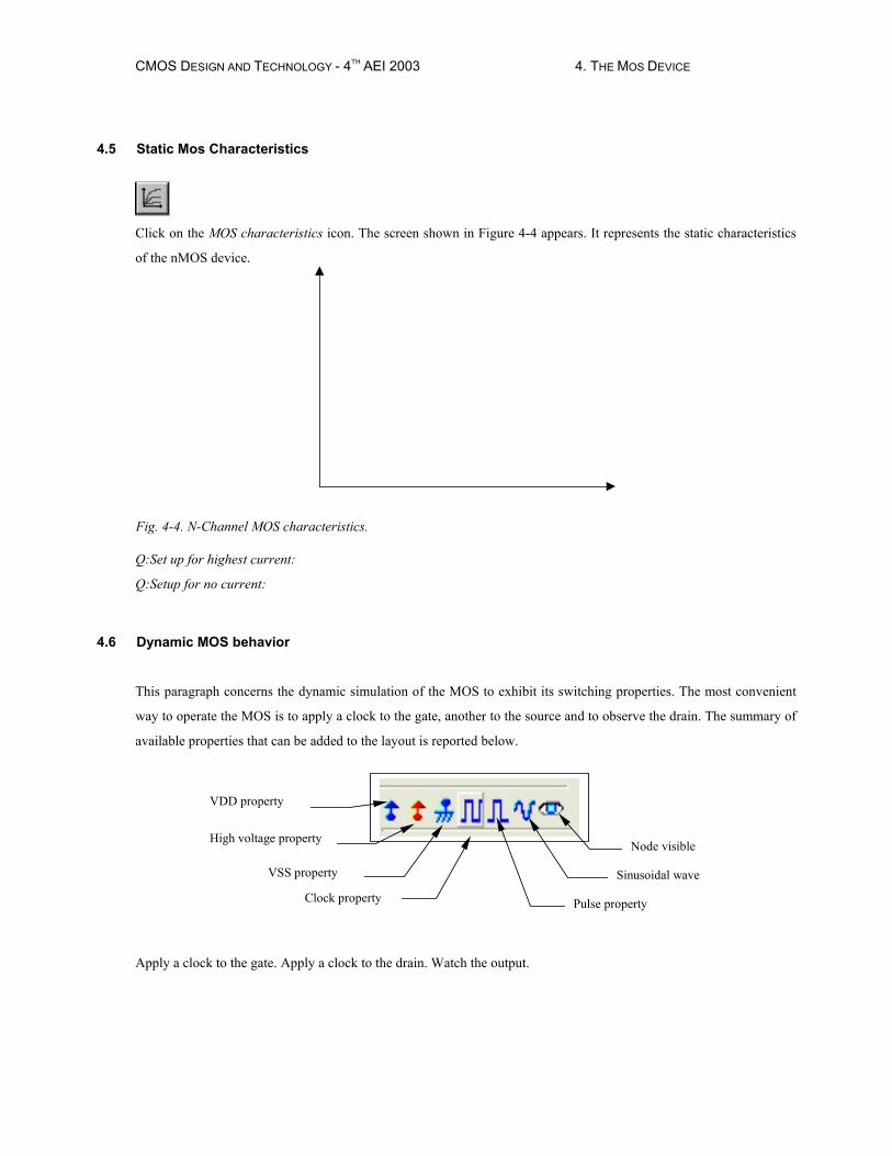
4.14 Process Variations
The simulated results should not be considered as absolute values. Due to unavoidable process variations during the
hundreds of chemical steps for the fabrication of the integrated circuit, the MOS characteristics are never exactly
identical from one device to another, and from one die to an other.
Fig. 4-20: The same MOS device may be fabricated with an important effective channel variation
The menu Simulate→Simulation parameters gives a simple access to minimum/typical/maximum parameter sets.
The approach has consisted in altering two main parameters: the threshold voltage (20% random variation, Gaussian
distribution) and the mobility (20% random variation). All other parameters are supposed to be constant.
Fig. 4-21: Access to minimum, typical, maximum model parameters or Random simulation
A comparative simulation of the Id/Vd curve in typical, maximum and minimum scenarios shows a very large variation
of performances.
Vds
Ids
Fig. 4-22: The MOS Id/vd curve in Min,Typ,Max modes.
CMOS DESIGN AND TECHNOLOGY - 4TH AEI 2003 4. THE MOS DEVICE
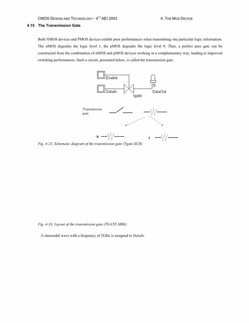
4.15 The Transmission Gate
Both NMOS devices and PMOS devices exhibit poor performances when transmitting one particular logic information.
The nMOS degrades the logic level 1, the pMOS degrades the logic level 0. Thus, a perfect pass gate can be
constructed from the combination of nMOS and pMOS devices working in a complementary way, leading to improved
switching performances. Such a circuit, presented below, is called the transmission gate.
Transmission gate
0 1 Fig. 4-23. Schematic diagram of the transmission gate (Tgate.SCH)
Fig. 4-24. Layout of the transmission gate (TGATE.MSK)
A sinusoidal wave with a frequency of 2GHz is assigned to DataIn.

CMOS DESIGN AND TECHNOLOGY - 4TH AEI 2003 4. THE MOS DEVICE
Fig. 4-25: Simulation of the transmission gate (TGATE.MSK)

CMOS DESIGN AND TECHNOLOGY- 4TH AEI 2003 5. THE INVERTER
Page 28 11/27/2003
This chapter describes the CMOS inverter at logic and layout level.
5.1 The Logic Inverter
Using DSCH2, click File→ Open in the main menu. Select INV.SCH in the list. In this circuit are one button situated
on the left side of the design, the inverter and a led. Click Simulate→ Start simulation in the main menu.
Fig. 5-.1: The logic Simulation Menu
Click the chronogram icon to get access to the chronograms of the previous simulation. As seen in the waveform, the
value of the output is the logic opposite of that of the input.
Fig. 5-2 Chronograms of the inverter simulation (CmosInv.SCH)
Double click on the INV symbol, the symbol properties window is activated. In this window appears the VERILOG
description (left side) and the list of pins (right side). A set of drawing options is also reported in the same window.
5 The Inverter

CMOS DESIGN AND TECHNOLOGY- 4TH AEI 2003 5. THE INVERTER
Page 29 11/27/2003
Q: What is the gate delay?
Q: What is the fanout effect?
5.2 THE CMOS INVERTER
The CMOS inverter design is detailed in the figure below. Here the p-channel MOS and the n-channel MOS transistors
function as switches. When the input signal is logic 0 (Fig. 5-3 left), the nMOS is switched off while PMOS passes
VDD through the output. When the input signal is logic 1 (Fig. 5-3 right), the pMOS is switched off while the nMOS
passes VSS to the output.
Fig. 5-3: The MOS Inverter (File CmosInv.sch)
5.3 MANUAL LAYOUT OF THE INVERTER
CMOS DESIGN AND TECHNOLOGY- 4TH AEI 2003 5. THE INVERTER
Page 30 11/27/2003
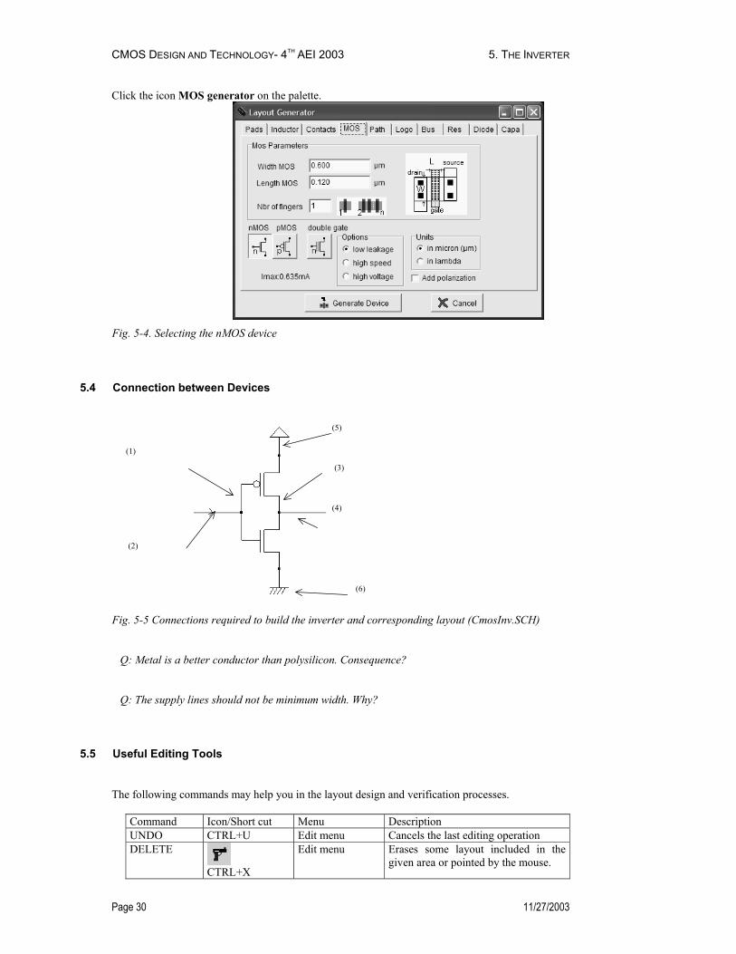
Click the icon MOS generator on the palette.
Fig. 5-4. Selecting the nMOS device
5.4 Connection between Devices
(1)
(2)
(5)
(6)
(4)
(3)
Fig. 5-5 Connections required to build the inverter and corresponding layout (CmosInv.SCH)
Q: Metal is a better conductor than polysilicon. Consequence?
Q: The supply lines should not be minimum width. Why?
5.5 Useful Editing Tools
The following commands may help you in the layout design and verification processes.
Command Icon/Short cut Menu Description UNDO CTRL+U Edit menu Cancels the last editing operation DELETE
CTRL+X
Edit menu Erases some layout included in the given area or pointed by the mouse.

CMOS DESIGN AND TECHNOLOGY- 4TH AEI 2003 5. THE INVERTER
Page 31 11/27/2003
STRETCH
Edit menu Changes the size of one box, or moves the layout included in the given area.
COPY
CTRL+C
Edit Menu Copies the layout included in the given area.
VIEW ELECTRICAL NODE
CTRL+N
View Menu Verifies the electrical net connections.
2D CROSS-SECTION
Simulate Menu Shows the aspect of the circuit in vertical cross-section.
Table 5-1: A set of useful editing tools
5.6 Metal-to-poly
As polysilicon is a poor conductor, metal is preferred to interconnect signals and supplies. Consequently, the input
connection of the inverter is made with metal. Metal and polysilicon are separated by an oxide which prevents
electrical connections. Therefore, a box of metal drawn across a box of polysilicon does not allow an electrical
connection. To build an electrical connection, a physical contact is needed. The corresponding layer is called
"contact".
Polysilicon (2 λ min)
Metal (4 λ min)
Fig. 5-4 Physical contact between metal and polysilicon
Fig. 5-5 Adding a poly contact, poly and metal bridges to construct the CMOS inverter (InvSteps.MSK)
The Process Simulator shows the vertical aspect of the layout, as when fabrication has been completed.

CMOS DESIGN AND TECHNOLOGY- 4TH AEI 2003 5. THE INVERTER
Page 32 11/27/2003
Fig.5-6 The 2D process section of the inverter circuit near the nMOS device (InvSteps.MSK)
5.7 Supply Connections
The next design step consists in adding supply connections, that is the positive supply VDD and the ground supply
VSS. In figure 5-7, we use the metal2 layer (Second level of metallization) to create horizontal supply connections.
Fig.5-7 Adding metal2 supply lines and the appropriate vias (InvSteps.MSK)
The simplest way to build the physical connection is to add a metal/Metal2 contact that may be found in the palette.
The connection is created by a plug called "via" between metal2 and metal layers.
The final layout design step consists in adding polarization contacts. These contacts convey the VSS and VDD voltage
supply close to the bulk regions of the device. Remember that the n-well region should always be polarized to a high
voltage to avoid short-circuit between VDD and VSS. Adding the VDD polarization in the n-well region is a very strict
rule.

CMOS DESIGN AND TECHNOLOGY- 4TH AEI 2003 5. THE INVERTER
Page 33 11/27/2003
P+/Pwell contact and bridge to VSS
N+/Nwell contact and bridge to VDD
Via to connect metal2 and metal 1
Fig.5-8 Adding polarization contacts
5.8 Process steps to build the Inverter
At that point, it might be interesting to illustrate the steps of fabrication as they would sequence in a foundry.
Microwind includes a 3D process viewer for that purpose. Click Simulate → Process steps in 3D.
Fig.5-9 The step-by-step fabrication of the Inverter circuit (InvSteps.MSK)
5.9 Inverter Simulation
The inverter simulation is conducted as follows. Firstly, a VDD supply source (1.2V) is fixed to the upper metal2
supply line, and a VSS supply source (0.0V) is fixed to the lower metal2 supply line. The properties are located in the
palette menu.

CMOS DESIGN AND TECHNOLOGY- 4TH AEI 2003 5. THE INVERTER
Page 34 11/27/2003
VDD
High VDDVSS Clock Pulse
Sinus
Visible
Fig.5-10 Adding simulation properties (InvSteps.MSK)
Q: Which properties do you assign to the CMOS inverter nodes?
Q: What are the typical clock parameters in 0.12µm?
The command Simulate → Run Simulation gives access to the analog simulation. Select the simulation mode Voltage
vs. Time. The time-domain analog simulation of the circuit is performed. This mode is also called transient simulation,
as shown below (.TRAN in SPICE).
Fig.5-11 Transient simulation of the CMOS inverter (InvSteps.MSK)
Q: What is the delay of the gate?
The simulation contains the supply currents in the upper window, and all voltage waveforms in the lower window.
Q: When does the main current consumption appears?

CMOS DESIGN AND TECHNOLOGY- 4TH AEI 2003 5. THE INVERTER
Page 35 11/27/2003
Fig. 5-12: Simulation of the current peaks in the CMOS inverter (InvSteps.MSK)
Fig. 5-13: Current consumption in log scale
5.10 General power Consumption
The power consumption computed by Microwind applies the formulation below. The power consumption appears at
the right corner of the simulation screen.

CMOS DESIGN AND TECHNOLOGY- 4TH AEI 2003 5. THE INVERTER
Page 36 11/27/2003
∑ ==
steps
n P
1
Three main factors contribute to the power consumption P: the load capacitance C, the supply voltage VDD and the
clock frequency f. For a CMOS inverter, this relation is usually represented by the first-order approximation below.
P =
Where:
k: technological factor (close to 1)
C: Output load capacitance (Farad)
VDD: supply voltage (V)
f: Clock frequency (Hz)
η: switching activity factor (Between 0 and 1)
5.11 3-STATE INVERTER
If two inverter outputs are connected together, it will provoke a circuit error. In order to avoid such conflicts, specific
symbols are used, featuring the possibility to remain in a ‘high impedance’ state. The 3-state symbol used below is
Bufif1, and it consists of the logic buffer and an enable control. There also exists a 3-state inverter Notif1. The output
remains in ‘high impedance’ as long as the enable ‘En’ is set to level ‘0’. The truth table of the 3-state inverter is
reported below.
NOTIF1
In En Out
Figure 5-14: Truth-table and schematic diagram of the 3-state inverter (CmosInv3State.SCH)

CMOS DESIGN AND TECHNOLOGY - 4TH AEI 2003 6. BASIC GATES
37 27/11/03
6.1 Introduction
Table 6-1 gives the corresponding symbol to each basic gate as it appears in the logic editor window as well as the
logic description.
Name Logic symbol Logic equation INVERTER
AND
NAND
OR
NOR
XOR
XNOR
Table 6-1. The list of basic gates
6.2 The Nand Gate
The truth-table and logic symbol of the NAND gate with 2 inputs are shown below. In DSCH, select the NAND
symbol in the palette, add two buttons and one lamp as shown above. Add interconnects if necessary to link the button
and lamps to the cell pins. Verify the logic behavior of the cell.
in1 in2 Out
Fig. 6-1. The truth table and symbol of the NAND gate
In CMOS design, the NAND gate consists of two nMOS in series connected to two pMOS in parallel. The schematic
diagram of the NAND cell is reported below. The nMOS in series tie the output to the ground for one single
combination A=1, B=1.
6 Basic Gates

CMOS DESIGN AND TECHNOLOGY - 4TH AEI 2003 6. BASIC GATES
38 27/11/03
Fig. 6-2. The truth table and schematic diagram of the CMOS NAND gate design (NandCmos.SCH)
Compilation
In Microwind2, click on Compile→Compile One Line. Select the line corresponding to the 2-input NAND description as shown above. The input and output names can be by the user modified.
Pmos devices
Nmos devices
Input A
Input B
NAND2 output
Cross-section A-A'
Cross-section B-B'
Click Compile. The result is reported above. The compiler has fixed the position of VDD power supply and the ground VSS. The texts A, B, and S have also been fixed to the layout. Default clocks are assigned to inputs A and B.
Fig. 6-3. A NAND cell created by the CMOS compiler.

CMOS DESIGN AND TECHNOLOGY - 4TH AEI 2003 6. BASIC GATES
39 27/11/03
Fig. 6-4. The nMOS devices in serial in the NAND gate
Q: Supply connection?
Q: Input,output connection?
6.3 The AND gate
In CMOS, the negative gates (NAND, NOR, INV) are faster and simpler than the non-negative gates (AND, OR,
Buffer).
Q: What is the arrangement to perform a continuous diffusion (More compact)?

CMOS DESIGN AND TECHNOLOGY - 4TH AEI 2003 6. BASIC GATES
40 27/11/03
Fig. 6-5: Layout and simulation of the AND gate
6.4 The 3-Input OR Gate
OR 3 Inputs A B C Or3
Fig. 6-6. The truth table and symbol of the OR3 gate
Fig. 6-7. Layout of the NOR gate
Q: What is the problem with 3-input OR simulation?

CMOS DESIGN AND TECHNOLOGY - 4TH AEI 2003 6. BASIC GATES
41 27/11/03
6.5 The XOR Gate
XOR 2 inputs A B OUT
Fig. 6-8. The basic schematic diagram of the XOR gate (XORCmos.SCH)
4-transistor implementation
Fig. 6-9. simulation of the XOR gate (XOR.MSK).
Q: What is the problem with 4T XOR?
Final solution : XOR 6 transistors
Fig. 6-10: Layout of the 6T XOR gate
CMOS DESIGN AND TECHNOLOGY - 4TH AEI 2003 6. BASIC GATES
42 27/11/03
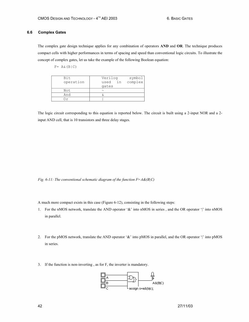
6.6 Complex Gates
The complex gate design technique applies for any combination of operators AND and OR. The technique produces
compact cells with higher performances in terms of spacing and speed than conventional logic circuits. To illustrate the
concept of complex gates, let us take the example of the following Boolean equation:
F= A&(B|C)
Bit operation
Verilog symbol used in complex gates
Not ~ And & Or |
The logic circuit corresponding to this equation is reported below. The circuit is built using a 2-input NOR and a 2-
input AND cell, that is 10 transistors and three delay stages.
Fig. 6-11: The conventional schematic diagram of the function F=A&(B|C)
A much more compact exists in this case (Figure 6-12), consisting in the following steps:
1. For the nMOS network, translate the AND operator ‘&’ into nMOS in series , and the OR operator ‘|’ into nMOS
in parallel.
2. For the pMOS network, translate the AND operator ‘&’ into pMOS in parallel, and the OR operator ‘|’ into pMOS
in series.
3. If the function is non-inverting , as for F, the inverter is mandatory.

CMOS DESIGN AND TECHNOLOGY - 4TH AEI 2003 6. BASIC GATES
43 27/11/03
Fig. 6-12: The complex gate implementation of the function F=A&(B|C)
Microwind2 is able to generate the CMOS layout corresponding to any description based on the operators AND and
OR, using the command Compile → Compile one line.
Fig. 6-12. A compiled complex gate and its analog simulation (ComplexABC.MSK)
Fig. 6-13. The complex gate symbol and its logic description
6.7 Multiplexor

CMOS DESIGN AND TECHNOLOGY - 4TH AEI 2003 6. BASIC GATES
44 27/11/03
Multiplexing means transmitting a large amount of information through a smaller number of connections. A digital
multiplexor is a circuit that selects binary information from one of many input logic signals and directs it to a single
input line. The main component of the multiplexor is a basic cell called the transmission gate. Sel In0 In1 f
Fig. 6-14. The transmission gate used as a multiplexor (MUX.SCH)
6.8 8 to 1 Multiplexor
The multiplexor is a very useful function and has a multitude of application. The selection of a particular input line is
controlled by a set of selection lines. Normally, there are 2n input lines and n selection lines whose bit combinations
determine which input is selected. Figure 6-15 shows the transmission gate implementation of the 8 to 1 multiplexor.
Fig. 6-15: 8 to 1 multiplexing based on transmission gates (Mux8to1.sch)
6.9 Interconnects and Vias
Up to 6 metal layers are available for signal connection and supply purpose. A significant gap exists between the
0.7µm 2-metal layer technology and the 0.12µm technology in terms of interconnect efficiency.

CMOS DESIGN AND TECHNOLOGY - 4TH AEI 2003 6. BASIC GATES
45 27/11/03
4 λ
N+ diff
Metal 2
N+ diff
Metal
(a) Contacts in 0.7µm technology (b) Contacts in 0.12µm technology
Metal 2
Metal
Figure 6-16: Contacts in 0.7µm technology require more area than in 0.12µm technology
Secondly, the stacking of contacts is not allowed in micro technologies. This means that a contact from poly to metal2
requires a significant silicon area as contacts must be drawn in a separate location. In deep-submicron technology
(Starting 0.35µm and below), stacked contacts are allowed.
4 λ minimum
4 λ Metal 2
Poly
Metal
4 λ minimum
Metal 2
(a) Poly to metal2 contact in 0.7µm technology (b) Poly to metal2 contact in 0.12µm technology
Poly Contact
Figure 6-17: Stacked vias are allowed in 0.12µm technology, which saves a significant amount of silicon area
compared to 0.7µm design style.
Metal layers are labeled according to the order in which they are fabricated, from the lower level 1 (metal 1) to the
upper level (metal 6 in 0.12µm). Each layer is embedded into a silicon oxide (SiO2) which isolates layers from each
other. The connection material between diffusion and metal is called "contact". The same layer is also used to connect
poly to metal, or poly2 to metal. The connection material between metal and metal2 is called "via". By extension, the
material that connects metal2 to metal3 is "via2", metal3 to metal4 "via3", etc..

CMOS DESIGN AND TECHNOLOGY - 4TH AEI 2003 6. BASIC GATES
46 27/11/03
Contactpoly/metal
Contact diffn/metal
Contact between selected layerand upper metal
Access to thecomplex contactmacro
via/metal
Selectedlayer
Diffp/Metal
Figure 6-18: Access to basic contact macros
Q: How many boxes in a Poly/Metal Contact?
Figure 6-19: The structure of a poly/Metal contact
Additionally, an access to complex stacked contacts is proposed thanks to the icon "complex contacts" situated in the palette, second row, second column. By default you create a contact from poly to metal1, and from metal1 to metal2. Change the tick to build more complex stacked contacts.
A convenient command exists in Microwind to add the appropriate contact between two layers. Let us imagine that we need to connect two signals, one routed in polysilicon and an other in metal3. Rather than invoking the complex macro command, we may just select the icon "connect layers". As a result a stack of contacts is inserted at the desired location to connect the lower layer to the upper layer.

CMOS DESIGN AND TECHNOLOGY - 4TH AEI 2003 7. Arithmetics
47 27/11/03
This chapter introduces basic concepts concerning the design of arithmetic gates. The adder circuit is presented, with
its corresponding layout created manually and automatically. Then the comparator, multiplier and the arithmetic and
logic unit are also discussed. This chapter also includes details on a student project concerning the design of binary-to-
decimal addition and display.
7.1 Unsigned Integer format
The two classes of data formats are the integer and real numbers. The integer type is separated into two formats:
unsigned format and signed format. The real numbers are also sub-divided into fixed point and floating point
descriptions. Each data is coded in 8,16 or 32 bits. We consider here unsigned integers, as described in figure 7-1.
26 25 24 23 20
20 = 1 21 = 2 22 = 4
23 = 8
24 = 16
25 = 32
26 = 64 27 = 128 …. 210 = 1024 215 = 32768 220 = 1048576 230 = 1073741824 231 = 2147483648
Unsigned integer, 8 bit
27 22 21
214 213 24 23.... 20
Unsigned integer, 16 bit
215 22 21
230 229 24 23.... 20
Unsigned integer, 32 bit
231 22 21..
Fig. 7-1. Unsigned integer format
7.2 Creating Arithmetic Circuits From Logic Design
When the design starts to be complex, the manual layout is very difficult to conduct, and an automatic approach is
preferred, at the price of a less compact design and more rigid implementation methodology. The steps from logic
design to layout validation are reported below. The schematic diagram constructed using DSCH is validated first at
logic level.
7 Arithmetics

CMOS DESIGN AND TECHNOLOGY - 4TH AEI 2003 7. Arithmetics
48 27/11/03
schematic
layout
Figure 7-2: Design flow from logic design to layout implementation
7.3 Half-Adder Gate
The Half-Adder gate truth-table and schematic diagram are shown below. The SUM function is made with an XOR
gate, the Carry function is a simple AND gate.
HALF ADDER
A B SUM CARRY
Fig. 7-3. Truth table and schematic diagram of the half-adder gate (HADD.MSK).
Q: Verilog description?
Fig. 7-4. Compiling and simulation of the half-adder gate (Hadd.MSK)
CMOS DESIGN AND TECHNOLOGY - 4TH AEI 2003 7. Arithmetics
49 27/11/03
7.4 Full-Adder Gate
Full Adder A B C Sum Carry
Fig. 7-5. The truth table and schematic diagram of a full-adder(FADD.SCH)
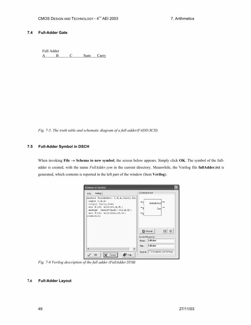
7.5 Full-Adder Symbol in DSCH
When invoking File → Schema to new symbol, the screen below appears. Simply click OK. The symbol of the full-
adder is created, with the name FullAdder.sym in the current directory. Meanwhile, the Verilog file fullAdder.txt is
generated, which contents is reported in the left part of the window (Item Verilog).
Fig. 7-6 Verilog description of the full adder (FullAdder.SYM)
7.6 Full-Adder Layout

CMOS DESIGN AND TECHNOLOGY - 4TH AEI 2003 7. Arithmetics
50 27/11/03
Fig. 7-7. The full adder compiled from the Verilog description (FullAdder.MSK)
7.7 Four-Bit Adder
The four-bit adder circuit includes adders in serial to perform the arithmetic addition. The result of each stage
propagates to the next one, from the right to left.
Fig. 7-8. Structure of the 4-bit ripple-carry adder

CMOS DESIGN AND TECHNOLOGY - 4TH AEI 2003 7. Arithmetics
51 27/11/03
Fig. 7-9. Manual design of the four-bit adder (ADD4.MSK).
Q: Supply strategy?
Q: stage propagation strategy?
Fig. 7-10. Simulation of the four-bit adder (ADD4.MSK).
Q: Weakness of carry-ripple strategy?

CMOS DESIGN AND TECHNOLOGY - 4TH AEI 2003 7. Arithmetics
52 27/11/03
7.8 Comparator
The truth table and the schematic diagram of the comparator are given below. The A=B equality represents an XNOR
gate, and A>B, A<B are operators obtained by using inverters and AND gates.
Comparator A B A>B A<B A=B
Fig. 7-11 The truth table and schematic diagram of the comparator (COMP.SCH).
Fig. 7-12. Simulation of a comparator (COMP.MSK).
7.9 Arithmetic and Logic Unit
The ALU is a digital function that implements basic micro-operations on the information stored in registers. In the
figure, the ALU receives the information from the registers A and B and performs a given operation as specified by the
control function F. The result is produced on S.

CMOS DESIGN AND TECHNOLOGY - 4TH AEI 2003 7. Arithmetics
53 27/11/03
Arithmetic and Logic Unit
8 bits 8 bits
Fig. 7-13. Principles for the Arithmetic and Logic Unit
Mnemonic Type Description CLR Clear Clear the accumulator CPL Complement Complements the accumulator, a bit or a memory contents.
All the bits will be reversed. ADD Addition Add the operand to the value of the accumulator, leaving the
resulting value in the accumulator. SUBB Substractor Subtracts the operand to the value of the accumulator, leaving
the resulting value in the accumulator. INC Increment Increment the content of the accumulator, the register or the
memory. DEC Decrement Decrement the content of the accumulator, the register or the
memory. XRL XOR operator Exclusive OR operation between the accumulator and the
operand, leaving the resulting value in the accumulator. ANL AND operator AND operation between the accumulator and the operand,
leaving the resulting value in accumulator. ORL OR operator OR operation between the accumulator and the operand,
leaving the resulting value in accumulator. RR Rotate right Shifts the bits of the accumulator to the right. The bit 0 is
loaded into bit 7. RL Rotate left Shifts the bits of the accumulator to the left. The bit 7 is
loaded into bit 0. Table 7-3. Some important instructions implemented in the ALU of the 8051 micro-controller
For example:
• ADD A,R0.
• SUBB A,#2
• INC A
• DEC A
• ANL A,#10
• ORL A,R7
• XRL A, R1

CMOS DESIGN AND TECHNOLOGY - 4TH AEI 2003 7. Arithmetics
54 27/11/03
Figure 7-14. The 8051 symbol and embedded software example (8051.SCH)
Figure 7-15. The simulation of the arithmetic and logic operation using the 8051 micro-controller (8051.SCH)
Dsch2 also includes the model of the PIC16f84 micro-controller. An example file can be found in 16f84adder.SCH.
Double click the 16f84 symbol, and click Assembly to convert the text lines into binary executable code. ; Simple program to add two numbers ; oper1 EQU 0x0c oper2 EQU 0x0d result EQU 0x0e org 0 movlw 5 movwf oper1 movlw 2 movwf oper2 movf oper1,0 addwf oper2,0 movwf result sleep

CMOS DESIGN AND TECHNOLOGY - 4TH AEI 2003 8. Latches
55 27/11/03
This chapter details the structure and behavior of latches and memory circuits. The RS Latch, the D Latch and the
edge-sensitive register are presenter. Then , the concepts of ROM, static RAM and dynamic RAM memories are
introduced, together with simulations.
8.1 Basic Latch
The basis for storing an elementary binary value is called a latch. The simplest CMOS circuit is made from 2 inverters.
Q
Q=10
1
2 stablememory
states
Q=01
0
Figure 8-1: Elementary memory cell based on an inverter loop
8.2 RS Latch
The RS Latch, also called Set-Reset Flip Flop (SR FF), transforms a pulse into a continuous state. The RS latch can be
made up of two interconnected NAND gates, inspired from the two chained inverters of figure 8-2. In that case, the
Reset and Set inputs are active low. The memory state corresponds to Reset=Set=1. The combination Reset=Set=0
should not be used, as Q=nQ=1. Furthermore, the simultaneous change from Reset=Set=0 to Reset=Set=1 provokes
what is called the metastable state, that corresponds to a parasitic ring effect that may jeopardize the behavior of the
whole circuit.
8 Latches

CMOS DESIGN AND TECHNOLOGY - 4TH AEI 2003 8. Latches
56 27/11/03
RS Latch (NAND) R S Q nQ 0 0 1 1 0 1 0 1 1 0 1 0 1 1 Q nQ
Fig. 8-2. The truth table and schematic diagram of a RS latch made (RSNor.SCH)
FULL CUSTOM LAYOUT. You may create the layout of RS latch manually. The two NAND gates may share the
VDD and VSS supply achieving continuous diffusions.
LAYOUT COMPILING. Use DSCH2 to create the schematic diagram of the RS latch. Verify the circuit with buttons
and lamps. Save the design under the name RS.sch using the command File → Save As. Generate the Verilog text by
using the command File → Make Verilog File. In Microwind2, click on the command Compile → Compile Verilog
File. Select the text file RS.txt. Click on Compile. When the compiling is complete, the resulting layout appears as
shown below. The NOR implementation of the RS gate is completed.
module RSNor( Reset,Set,Q,nQ); input Reset,Set; output Q,nQ; nor nor1(Q,nQ,Reset); nor nor2(nQ,Set,Q); endmodule
With the Reset and Set signals behaving like clocks, the memory effect is not easy to illustrate. A much better approach
consists in declaring pulse signals with an active pulse on Reset followed by an active pulse on Set. Consequently, you
must change the clock property into a pulse property. For NOR implementation, the pulse is positive.
1. Select the Pulse icon. Click on the node Reset.
2. Click the brush to clear the existing pulse properties of the pulse.
3. Enter the desired sequence, for example 01000, and click Insert. A piece-wise-linear sequence is generated in the
table, describing the 01000 waveform in an analog way.

CMOS DESIGN AND TECHNOLOGY - 4TH AEI 2003 8. Latches
57 27/11/03
Fig. 8-3. The pulse property used to control the Reset of the latch (RsNor.MSK)
Fig. 8-4. Layout of the RS latch made (RSNor.MSK)
4. Repeat the same procedure to change the clock into a pulse for node Set. This time the sequence must be 000100 to
delay the pulse.
5. Click on Simulate →Start Simulation. The timing diagrams of figure 8-5 appear. Click on Close to return to the
editor.
In the simulation, a positive pulse on Set turns Q to a stable high state. Notice that when Set goes to 0, Q remains at 1,
which is called the ‘memory’ state. When a positive pulse occurs on Reset, Q goes low, nQ goes high. In this type of
simulation, the combination Reset=Set=1 is not present.

CMOS DESIGN AND TECHNOLOGY - 4TH AEI 2003 8. Latches
58 27/11/03
Fig. 8-5. Simulation of the RSNOR latch (RSNor.MSK)
8.3 D Latch
The truth table and schematic diagram of the static D latch, also called Static D-Flip-Flop, are shown in Figure 7-6. The
data input D is transferred to the output if the clock input is at level 1. When the clock returns to level 0, the latch keeps
its last value.
D Latch (NOR) D Clock Q nQ 0 0 Q nQ 0 1 0 1 1 0 Q nQ 1 1 1 0
Fig. 8-6. The truth table and schematic diagram of a D Latch (File DLATCH.SCH).
MANUAL DESIGN. Note that the NOR2-AND combination can be implemented in a complex-gate style. You may
find useful to invoke the one line compiler to create successively one inverter nd=~d, and two complex gates which
include the AND/NOR cells.
Q: Syntax? Q= nQ=
Assign a clock to Clk and a clock to Data. An example of such an implementation can be found in the file
DLatchCompile.MSK. Its layout an corresponding simulation are illustrated in figure 8-7.

CMOS DESIGN AND TECHNOLOGY - 4TH AEI 2003 8. Latches
59 27/11/03
Fig. 8-7 Implementation of the D Latch (File DlatchCompile.MSK)
Figure 8-8: The compiled Dlatch at work (DlatchCompile.MSK).
The simulation is reported in figure 8-8. The default clocks assigned during compilation have been modified. The
parameters of the clock Data have been changed to avoid the perfect synchronization with clock1, in order to watch in
one single simulation several situations. When clock1 is asserted, the logic information contained in Data is transferred
to Q, its inverted value to nQ. When clock1 falls down to 0, Q and nQ keep in memory state.

CMOS DESIGN AND TECHNOLOGY - 4TH AEI 2003 8. Latches
60 27/11/03
8.4 Edge Trigged Latch
The most common example of an edge-trigged flip flop is the JK latch. Anyhow, the JK is rarely used, a more simple
version that features the same function with one single input D is preferred. This simple type of edge-trigged latch is
one of the most widely used cells in microelectronics circuit design. The cell structure comprises two master-slave
basic memory stages.
The most compact implementation of the edge-trigged latch is reported below. The schematic diagram is based on
inverters and pass-transistors. On the left side, the two chained inverter are in memory state when the pMOS loop
transistor P1 is on, that is when Clk=0. The two-chained inverters on the right side act in an opposite way. The reset
function is obtained by a direct ground connection of the master and slave memories, using nMOS devices.
Master memory cell Slave memory cell
Figure 8-9 : The edge-trigged latch and its logic simulation (Dreg.MSK)
Notice that the logic model of the MOS device is not working the same way as for the real MOS switch. In the case of
the logic implementation, the logic signal flows only from the source to the drain. This is not the case of the real switch
where the signal can flow both ways.
In figure 8-10, clock is high, the master latch is updated to a new value of the input D. The slave latch produces to the
output Q the previous value of D. When clock goes down, the master latch turns to memory state. The slave circuit is
updated. The change of the clock from 1 to 0 is the active edge of the clock. This type of latch is a negative edge flip
flop.

CMOS DESIGN AND TECHNOLOGY - 4TH AEI 2003 8. Latches
61 27/11/03
Figure 8-10 The edge-trigged latch and its logic simulation (Dreg.MSK)
Use the Verilog compiler to generate the edge-trigged latch, using the following text (dreg.txt), or by creating a
schematic diagram including the “D” register symbol, in the symbol palette of DSCH2. As can be seen, the register is
built up from one single call to the primitive dreg. For simulation:
• Reset is active on a level 1. Reset is activated twice, at the beginning and later, using a piece-wise linear
description included in the pulse property.
• Clk is a clock with 10ns at 0 and 10ns at 1.
• D is the data chosen here not synchronized with Clk, in order to observe various behaviors of the register.
To compile the DREG file, use the command Compile→Compile Verilog Text. The corresponding layout is reported
below. The piece-wise-linear data is transferred to the text “rst” automatically.

CMOS DESIGN AND TECHNOLOGY - 4TH AEI 2003 8. Latches
62 27/11/03
Master memory loopSlave memory loop
Reset master Reset slave
Fig. 8-11: Compiled version of the Edge-trigged D Flip Flop (DregCompile.MSK)
For testing the Dreg, the Reset signal is activated twice, at the beginning and later, using a piece-wise linear property.
The Clock signal has a 2ns period. D is the data chosen here not synchronized with Clock, in order to observe various
behaviors of the register.
The simulation of the edge-trigged D-register is reported in figure 8-12. The signals Q and nQ always act in opposite.
When Reset is asserted, the output Q is 0, nQ is 1. at a fall edge of the clock.
Fig. 8-12 Simulation of the DREG cell (DregCompile.MSK) Q: When does Q take the value of D? Q: To which edge of Clock is this latch sensitive?

CMOS DESIGN AND TECHNOLOGY - 4TH AEI 2003 8. Latches
63 27/11/03
8.5 Counter
The one-bit counter is able to produce a signal featuring half the frequency of a clock. The most simple implementation
consists of a D flip-flop where the output nQ is connected to D, as shown below. In the logic simulation, the clock
changes the state of ClockDiv2 at each fall edge. The Reset signal is active high, and stuck the output to 0.
Fig. 8-13. Schematic diagram and simulation of the counter (ClockDiv2.SCH).
Fig 8-14. Layout of the divider-by-two (ClockDiv2.MSK)

CMOS DESIGN AND TECHNOLOGY - 4TH AEI 2003 9. FPGA Principles
64 27/11/03
Field programmable gate arrays (FPGA) are specific integrated circuits that can be user-programmed easily. The FPGA
contains versatile functions, configurable interconnects and input/output interface to adapt to the user specification.
Modern FPGA are extremely dense, with complexity of several millions of gates which enable the emulation of very
complex hardware such as parallel microprocessors, mixture of processor and signal processing, etc…
Q: Main advantage of FPGA?
Q: FPGA in Airbus?
Q: FPGA in electronic car control?
Programmable logicblocks
ConfiguredI/O pads
Programmableinterconnect points
Figure 9-1: Basic structure of a field programmable gate array
A
B
Programmable logic block
configured as XOR
f=A^B^C
Pads configured as inputs
Pad configured as output
Programmable interconnect
points
Interconnect lines
C
Figure 9-2: Using a field programmable gate array to build a 3-input XOR gate
9 FPGA Principles

CMOS DESIGN AND TECHNOLOGY - 4TH AEI 2003 9. FPGA Principles
65 27/11/03
FPGA
(a) Stand-alone FPGA (b) FPGA internal block
Figure 9-3: FPGA exist as stand-alone Ics or blocs within a system-on-chip
9.1 MULTIPLEXORS
Surprisingly, a two-input multiplexor can be used as a programmable function generator, as illustrated in figure 9-4.
Recall that the multiplexor output f is equal to i0 if en=0, and i1 if en=1.
Function Boolean expression for output f i0 i1 en BUF(A) NOT(A) AND(A,B) OR(A,B)
Figure 9-4: use of multiplexor to build logic functions
Figure 9-5: Use of multiplexor to build an inverter
Q: How to implement a NAND, NOR, XOR ?
Figure 9-6: Multiplexor to build a NAND

CMOS DESIGN AND TECHNOLOGY - 4TH AEI 2003 9. FPGA Principles
66 27/11/03
9.2 Look Up Table
The look-up table (LUT) is by far the most versatile circuit to create a configurable logic function. The look-up table
shown in figure 9-7 has 3 main inputs F0,F1 and F2. The main output is Fout, which is a logical function of F0, F1
and F2. The output Fout is defined by the values given to Value[0]..Value[7].
F0
F1
F2 Fout
Value[0]
Value[1]
Value[2]
Value[3]
Value[4]
Value[5
Value[6]
Value[7]
Look-up-table
0
1
1
i=5
Function Value[0] Value[1] Value[2] Value[3] Value[4] Value[5] Value[6] Value[7] ~F0 ~F1 ~F2 F0&F1 F0|F1|F2 F0^F1^F2
Figure 9-7: Link between basic logic functions and
Logic inputs F0,F1 and F2
Each value is assigned the
XOR3 truth-table data
Fout=F0^F1^F2
Elementary cell for the 3-to-8 demultiplexor
~F0&~F1&~F2
F0&~F1&~F2
~F0&F1&~F2
F0&F1&~F2
~F0&~F1&F2
F0&~F1&F2
~F0&F1&F2
F0&F1&F2
Figure 9-8: The output f produces a logical function Fout according to a look-up-table stored in memory points
Value[i] (FpgaLutStructure.SCH)

CMOS DESIGN AND TECHNOLOGY - 4TH AEI 2003 9. FPGA Principles
67 27/11/03
9.3 Memory Points
Memory points are essential components of the configurable logic blocks. The memory point is used to store one
logical value, corresponding to the logic truth table. For a 3-input function (F0,F1,F2 in the previous LUT), we need an
array of 8 memory points to store the information Value[0]..Value[7]. There exist here also several approaches to store
one single bit of information. The one that is illustrated below consists of D-reg cells. Each register stores one logical
information Value[i]. The Dreg cells are chained in order to limit the control signals to one clock ClockProg and one
data signal DataProg.
Figure 9-9: The look-up information is given by a shift register based on D-reg cells (FpgaLutDreg.sch).
Figure 9-10: At the end of the 8-th clock period, the LUT is configured as a 3-input XOR (FpgaLutDreg.sch)
CMOS DESIGN AND TECHNOLOGY - 4TH AEI 2003 9. FPGA Principles
68 27/11/03
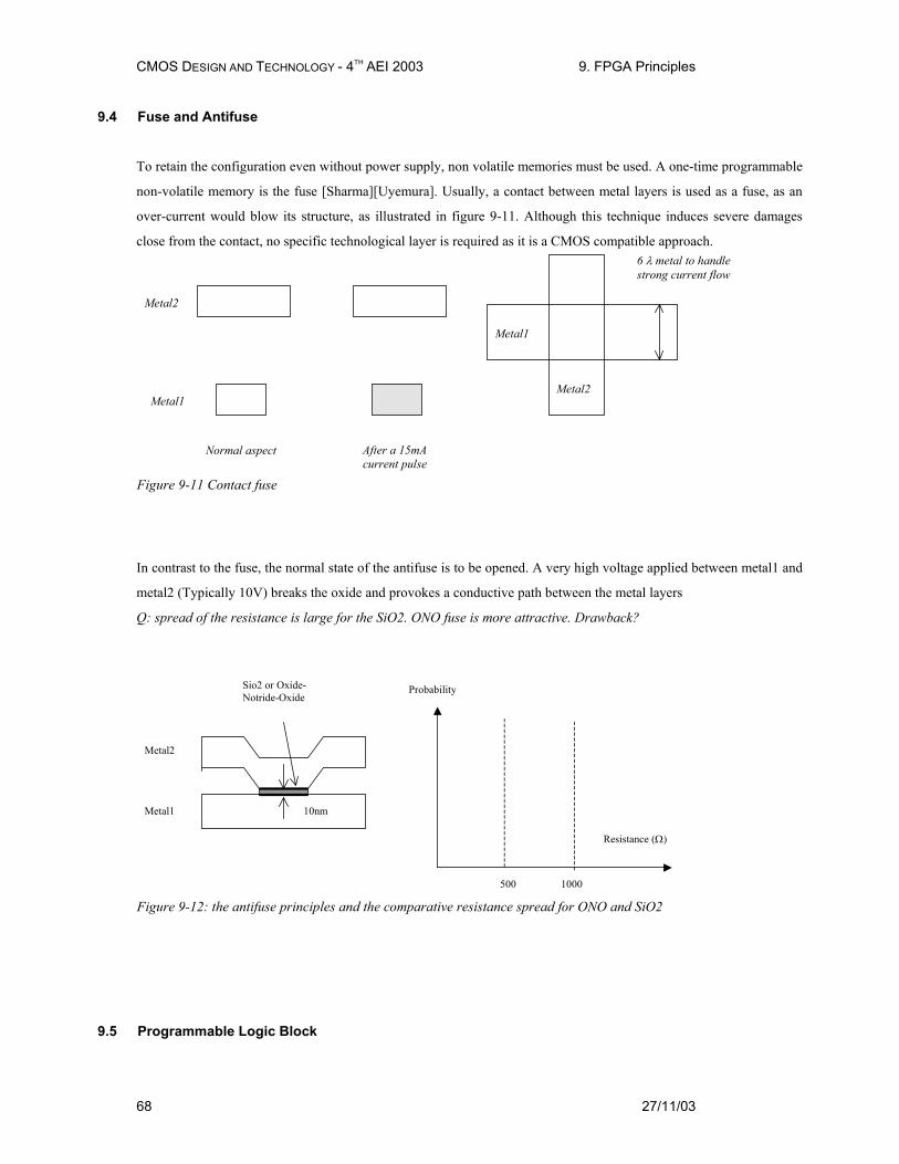
9.4 Fuse and Antifuse
To retain the configuration even without power supply, non volatile memories must be used. A one-time programmable
non-volatile memory is the fuse [Sharma][Uyemura]. Usually, a contact between metal layers is used as a fuse, as an
over-current would blow its structure, as illustrated in figure 9-11. Although this technique induces severe damages
close from the contact, no specific technological layer is required as it is a CMOS compatible approach.
Normal aspect
Metal2
Metal1
After a 15mA current pulse
6 λ metal to handle strong current flow
Metal1
Metal2
Figure 9-11 Contact fuse
In contrast to the fuse, the normal state of the antifuse is to be opened. A very high voltage applied between metal1 and
metal2 (Typically 10V) breaks the oxide and provokes a conductive path between the metal layers
Q: spread of the resistance is large for the SiO2. ONO fuse is more attractive. Drawback?
Resistance (Ω)
Probability
500 1000
Sio2 or Oxide-Notride-Oxide
10nm Metal1
Metal2
Figure 9-12: the antifuse principles and the comparative resistance spread for ONO and SiO2
9.5 Programmable Logic Block

CMOS DESIGN AND TECHNOLOGY - 4TH AEI 2003 9. FPGA Principles
69 27/11/03
The programmable logic block consists of a look-up table, a D-register and some multiplexor. We present in figure 9-
13 a simple structure, which has some similarities with the Xilinx XC5200 series (See [Smith] for detailed information
on its internal structure).
Figure 9-13: Simple configurable logic block including the Look Up Table and a D-register (FpgaCell.SCH)
Figure 9-14: The Look Up Table, the D-register and the shift register including the 2 multiplexor cells
(FpgaBlockStructure.SCH)
Q: How many active clock edges to configure the block?

CMOS DESIGN AND TECHNOLOGY - 4TH AEI 2003 9. FPGA Principles
70 27/11/03
Dreg0DataProg
ClockProg
Dreg1 Dreg2 Dreg9
Clock cycle
1 2 3 4 5 6 7 8 9 10
DataProg
Figure 9-15: Serial data information used to program the LUT memory points
9.6 Interconnection between blocks
The interconnection strategy between logic blocks is detailed in this paragraph. We focus on the programmable
interconnect point and the programmable switching matrix. The PIP may have two states: "On" and "Off". You may
switch from "On" to "Off" by a double click on the symbol and a click in the button "On/off".
Figure 9-16: Changing the state of the PIP (FpgaPip.SCH)
The bridge can be built from a transmission gate, controlled once again by a D-reg cell. When the register information
contains a 0, the transmission gate is off and no link exists between Interco1 and Interco2. When the information hold
by the register is 1, the transmission gate establishes a resistive link between Interco1 and Interco2. The resistance
value is around 100 Ω.
(a) Switch off (b) Swicth on
Figure 9-17: Internal structure of the PIP and illustration of its behavior when Off (a) and On (b) (FpgaPip.SCH)

CMOS DESIGN AND TECHNOLOGY - 4TH AEI 2003 9. FPGA Principles
71 27/11/03
The regrouping of programmable interconnect points into matrix is of key importance to ensure the largest routing
flexibility. A specific routing tool usually handles this task, but the manual re-arrangement is not rare in some complex
situations.
Figure 9-18: Matrix of programmable interconnects points (FpgaPip.SCH)
9.7 Switching Matrix
The switching matrix is a sophisticated programmable interconnect point, which enables a wide range of routing
combinations within a single interconnect crossing.
Click on oneof these 6switches toconfigure therouting
Figure 9-19: Changing the state of the matrix (FpgaMatrix.SCH)

CMOS DESIGN AND TECHNOLOGY - 4TH AEI 2003 9. FPGA Principles
72 27/11/03
Figure 9-20: 3x2 switching matrix and example of routing strategy between 6 inputs and outputs (fpgaMatrix.SCH)
Examples of 3x2 and 3x3 switching matrix are given in figure 9-20. The routing possibilities are numerous, which
improves the configurability of the logic blocs.
9.8 Implementation of the Switching Matrix
From a practical point of view, the switching matrix can be built from a regrouping of 6 transmission gates (Figure 9-
21). Each transmission gate is controlled by an associated Dreg cell, which memories the desired configuration. The
Dreg cells are chained so that one single input DataIn and one clock LoadClock are enough to configure the matrix.
Figure 9-21: The transmission gates placed on the routing lines to build the matrix (FpgaMatrix3.SCH)
CMOS DESIGN AND TECHNOLOGY - 4TH AEI 2003 9. FPGA Principles
73 27/11/03
9.9 Array of Blocs
The configurable blocs are associated with programmable interconnect points and switching matrix to create a
complete configurable core. An example of double configurable block and its associated configurable routing is
proposed in figure 9-22.
Global clock
Global reset
Block configurationdata
Configurable I/Os
PIP
Switchingmatrix
Figure 9-22: Configurable blocks, switching matrix, configurable I/Os and arrays of PIP (fpga2blocks.SCH)
Block 1 (SUM)
Block 2 (CARRY)
A, B, C Sum Carry
Figure 9-23: The SUM and CARRY functions to realize the full-adder in FPGA (fpgaFullAdder.SCH)
Block 1 (Sum of F0,F1 and F2) Cycle 1 2 3 4 5 6 7 8 9 10 DataIn Nq
DatainFout
Val[7] Val[6] Val[5] Val[4] Val[3] Val[2] Val[1] Val[0]
0 0 1 0 0 1 0 1 1 0
Block 2 (Carry of F0,F1 and F2) Cycle 1 2 3 4 5 6 7 8 9 10 DataIn Nq
DatainFout
Val[7] Val[6] Val[5] Val[4] Val[3] Val[2] Val[1] Val[0]
0 0 1 1 1 0 1 1 0 0
Table 9-4. Serial data used to configure the logic blocks 1&2 as SUM and CARRY

CMOS DESIGN AND TECHNOLOGY - 4TH AEI 2003 9. FPGA Principles
74 27/11/03
Figure 9-24: Simulation of the full-adder implemented in 2 configurable blocks (fpgaFullAdder.SCH)

CMOS DESIGN AND TECHNOLOGY - 4TH AEI 2003 10.Memories
75 27/11/03
10.1 The world of Memory
Semiconductor memories are vital components in modern integrated circuits. Stand-alone memories
represent roughly 30% of the global integrated circuit market. Within system-on-chip, memory circuits
usually represent more than 75% of the total number of transistors.
CMOS memories
Volatile memories Non volatile memories
Dynamic
• DRAM • SDRAM • EDO • DDRAM
Static
• SRAM • Dual port SRAM
Fixed
• ROM
One-time programmable
• PROM
Erasable & programmable
• EPROM • EEPROM • FLASH • MRAM • FRAM
Figure 10-1 Major classes of CMOS compatible memories
Two main families of devices exist: volatile and non-volatile memories.
o In volatile circuits (Figure 10-1 left), the data is stored as long as the power is applied. The
dynamic random access memory (DRAM) is the most common memory.
o Non-volatile memories are capable of storing the information even if the power is turned off
(Figure 10-1 right). The read-only memory (ROM) is the simplest type of non-volatile memory.
One-time programmable memories (PROM) are a second important family, but the most popular
non volatile memories are erasable and programmable devices: the old electrically
programmable ROM (EPROM), the more recent Electrically Erasable PROM (EEPROM,
FLASH), and the new magneto resistive RAM ( MRAM) and ferroelectric RAM (FRAM)
memories.
10 Memory Circuits
CMOS DESIGN AND TECHNOLOGY - 4TH AEI 2003 10.Memories
76 27/11/03
ROW
SELECT
Column Select
Read/Write Circuit
1 M
Columnaddress
DataOut DataIn
1
N
2N rows
Rowaddress
2N x 2M bit ofmemory
2M columns
Selectedmemory cellSelected row
Selected column
Figure 10-2 Typical memory organization
Figure 10-2 shows a typical memory organization schematic. It consists of a memory array, a row
decoder, a column decoder and a read/write circuit. The row decoder selects one row from 2N, thanks to a
N-bit row selection address. The column decoder selects one row from 2M, thanks to a M-bit column
selection address. The memory array is based on 2N rows and 2M columns of a repeated pattern, the basic
memory cell.
Q: How many bA typical value for N and M is 10, leading to 1024 rows and 1024 columns, that
corresponds to 1048576 elementary memory cells (1Mega-bit).
10.2 RAM Memory
The basic cell for static memory design is based on 6 transistors, with two pass gates instead of one. The
corresponding schematic diagram is given below. The circuit consists again of the 2 cross-coupled
inverters, but uses two pass transistors instead of one. The cell has been designed to be duplicated in X
and Y in order to create a large array of cells. Usual sizes for Megabit SRAM memories are 256 column x
256 rows or higher. A modest arrangement of 4x4 RAM cells is also proposed. The selection lines WL
concerns all the cells of one row. The bit lines BL and ~BL concern all the cells of one column.
CMOS DESIGN AND TECHNOLOGY - 4TH AEI 2003 10.Memories
77 27/11/03
Figure 10-3: The layout of the 6 transistor static memory cell (RAM6T.SCH)
Fig. 10-4 An array of 6T memory cells, with 4 rows and 4 columns (RAM6T.SCH)
The RAM layout is given in Figure 10-5. The BL and ~BL signals are made with metal2 and cross the cell
from top to bottom. The supply lines are horizontal, made with metal3. This allows easy matrix-style
duplication of the RAM cell.
Fig. 10-5. The layout of the static RAM cell (RAM6T.MSK).

CMOS DESIGN AND TECHNOLOGY - 4TH AEI 2003 10.Memories
78 27/11/03
WRITE CYCLE. Values 1 or 0 must be placed on Bit Line, and the data inverted value on ~Bit Line.
Then the selection Word Line goes to 1. The two-inverter latch takes the Bit Line value. When the
selection Word Line returns to 0, the RAM is in a memory state.
READ CYCLE. The selection signal Word Line must be asserted, but no information should be imposed
on the bit lines. In that case, the stored data value propagates to Bit Line, and its inverted value ~Data
propagates to ~Bit Line.
SIMULATION. The simulation parameters correspond to the read and write cycle in the RAM. The
proposed simulation steps consist in writing a 0, a 1, and then reading the 1. In a second phase, we write a
1, a 0, and read the 0. The Bit Line and ~Bit Line signals are controlled by pulses. The floating state is
obtained by inserting the letter "x" instead of 1 or 0 in the description of the signal.
Fig. 10-6. The bit Line pulse used the "x" floating state to enable reading the memory cell
(RamStatic6T.MSK)
The simulation of the RAM cell is proposed in figure 10-7.
Q:? Is Data initial value predictable?
Q: When does the memory cell information Data goes down to 0?
Q: When does the memory cell information Data goes to 1?
Q: When is the read cycle?

CMOS DESIGN AND TECHNOLOGY - 4TH AEI 2003 10.Memories
79 27/11/03
Fig. 10-7. Write cycle for the static RAM cell (RamStatic6T.MSK).
10.3 RAM Array
You can duplicate the RAM cell into a 4x4 bit array using the command Edit → Duplicate XY. A very
interesting approach to obtain a more compact memory cell consists in sharing all possible contacts: the
supply contact, the ground contact and the bit line contacts. The consequence is that the effective cell size
can be significantly reduced.
Sharedcontact
N1
N3
N2
N4
P1 P2
Figure 10-8. Sharing all possible contacts lead to a very compact cell design (Ram6Tcompact.MSK)

CMOS DESIGN AND TECHNOLOGY - 4TH AEI 2003 10.Memories
80 27/11/03
The layout is functionally identical to the previous layout. The only difference is the placement of MOS
devices and contacts. We duplicate the RAM cell into a 64 bit array. The multiplication cannot be done
directly by the command Duplicate XY, as we need to flip horizontally one cell to share lateral contacts,
and flip vertically the resulting block to share vertical contacts (Figure 10-9).
Figure 10-9. Compact 16x4 array of memory cells with shared contacts (Ram16x4Compact.MSK)
10.4 Row Selection Circuit
The row selection circuit decodes the row address and activates one single row. This row is shared by all
word line signals of the row. The row selection circuit is based on a multiplexor circuit. One line is
asserted while all the other lines are at zero.

CMOS DESIGN AND TECHNOLOGY - 4TH AEI 2003 10.Memories
81 27/11/03
ROW
SELECT
1
N
2N rows
Rowaddress
Selected row (Word Line)
MemRow CellHeight
fixed bythe Mem
size
Freewidth
Memwidth
Memheight
WordLineWord
Line
Fig. 10-10 The row selection circuit
In the row selection circuit for the 16x4 array, we simply need to decode a two-bit address. Using AND
gates is one simple solution. In figure 10-11, we present the schematic diagram of 2-to-4 and 3-to-8
decoders. In the case of very large number of address lines, the decoder is split into sub-decoders, which
handle a reduced number of address lines.
Fig. 10-11. The row selection circuit in 2 bit and 3 bit configuration (RamWordLine.SCH)

CMOS DESIGN AND TECHNOLOGY - 4TH AEI 2003 10.Memories
82 27/11/03
10.5 Column Selection Circuit
Column Select
Read/Write Circuit
1 M
Columnaddress
DataOut DataIn
2M columns
Selectedmemory cell
Selected column
Control
Figure 10-12. The column selection circuit principles
The column decoder selects a particular column in the memory array for reading the contents of the
selected memory cell (Figure 10-12) or to modify its contents. The column selector is based on the same
principles as those of the row decoder.
Q: What is the major modification ?
Figure 10-13 proposes an architecture based on n-channel MOS pass transistors. We consider here 4
columns of memory cells, which requires 2 address signals Address_Col[0] and Address_Col[1]. The n-
channel MOS device is used as a switch controlled by the column selection.
Figure 10-13. Row selection and Read/Write circuit (RamColumn.SCH)
Q: Behavior of the circuit?

CMOS DESIGN AND TECHNOLOGY - 4TH AEI 2003 10.Memories
83 27/11/03
10.6 A Complete 64 bit SRAM
The 64 bit SRAM memory interface is shown in figure 10-14. The 64 bits of memory are organized in
words of 4 bits, meaning that DataIn and DataOut have a 4 bit width. Each data D0..D15 occupies 4
contiguous memory cells in the array. Four address lines are necessary to decode the one address among
16. The memory structure shown in figure 10-14 requires two address lines A0 and A1 for the word lines
WL[0]..WL[3] and two address lines A2 and A3 for the bit line selection.
Address bus
A0 A1
WE Read/Write
Clk Clock
Do0
Do1
Data Out bus
CE
Chip Enable
Do2
Do3
Di0 Di1
Di3 Data In bus
Di2
A2 A3
64 bit SRAM(16x4 bit)
D0
D1
D2
D3
D4
D5
D6
D7
D8
D9
D10
D11
D12
D13
D14
D15
Each Data has a 4 bit size
WL3
WL2
WL1
WL0
A0..1
Figure 10-14. The architecture of the 64 bit RAM (RAM64.MSK)
Figure 10-15. The complete RAM layout (RAM64.MSK)

CMOS DESIGN AND TECHNOLOGY - 4TH AEI 2003 10.Memories
84 27/11/03
10.7 Dynamic RAM Memory
The dynamic RAM memory has only one transistor, in order to improve by almost one order of
magnitude the memory matrix density. The storage element is no more the stable inverter loop as for the
static RAM, but only a capacitor Cs, also called the storage capacitor. The DRAM cell architecture is
shown in figure 10-16.
Figure 10-16: Simulation of the Write cycle for the 1 transistor dynamic RAM cell (RAM1T.SCH)
The write and hold operation for a "1" is shown in figure 10-17. The data is set on the bit line, the word
line is then activated and Cs is charged. When WL is inactive, the storage capacitor Cs holds the "1".
Q: What is the analog voltage of Cs?
Figure 10-17: Simulation of the Read cycle for the 1 transistor dynamic RAM cell (RAM1T.SCH)
The reading cycle is destructive for the stored information. Suppose that Cs holds a 1. The bit line is
precharged to a voltage Vp (Usually around VDD/2). When the word line is active, a communication is
established between the bit line, loaded by capacitor CBL, and the memory, loaded by capacitor CS.
Q: What is resulting voltage?

CMOS DESIGN AND TECHNOLOGY - 4TH AEI 2003 10.Memories
85 27/11/03
Commercial dynamic RAM memories use storage capacitors with a value between 10fF and 50fF. This is
done by creating a specific capacitor for the storage node appearing in figure 10-18 left, thanks to the
following technological advances: use of specific metal layer to create the lower plate and external walls
of the RAM capacitor, enlarged height between the substrate surface and metal1, and use of high
permittivity dielectric oxide. The silicon dioxide SiO2 has a relative permittivity εr of 3.9.
Q: What are the other oxides?
Metal 1
Bit Line
Word Line
N+ diffusion
Substrate (ground)
Small Cs
Metal 1
Bit Line
Word Line
Specific metal
Specific Poly (Ground)
Substrate
Large height
High K dielectric
Very large Cs
External walls
Figure 10-18: Increasing the storage capacitance (Left: junction capacitor, right, embedded capacitor)
The cross-section of the DRAM capacitor is given in figure 10-19. The capacitance is around 20fF is this
design. Higher capacitance values may be obtained using larger option layer areas, at the price of a lower
cell density.
Q: Bit, line? Word line?
Q: Capacitor grounding?
Figure 10-19: The stacked capacitor cell compared to the diffusion capacitor cell (DramEdram.MSK)
CMOS DESIGN AND TECHNOLOGY - 4TH AEI 2003 10.Memories
86 27/11/03
10.8 EEPROM
The basic element of an EEPROM (Electrically Erasable PROM) memory is the floating-gate transistor.
The concept was introduced several years ago for the EPROM (Erasable PROM). It is based on the
possibility of trapping electrons in an isolated polysilicon layer placed between the channel and the
controlled gate.
Q: Influence of trapped electrons?
When there is no charge in the floating gate (Figure 10-20, upper part), the threshold voltage is low,
meaning that a significant current may flow between the source and the drain, if a high voltage is applied
on the gate. However, the channel is small as compared to a regular MOS, and the Ion current is 3 to 5
times lower, for the same channel size.
Fig. 10-20: The two states of the double gate MOS (EepromExplain.SCH)
When charges are trapped in the floating polysilicon layer (Figure 10-20, lower part), the threshold
voltage is high, almost no current flows through the device, independently of the gate value. As a matter
of fact, the electrons trapped in the floating gate prevent the creation of the channel by repealing channel
electrons. Data retention is a key feature of EEPROM, as it must be guaranteed for a wide range of
temperatures and operating conditions. Optimum electrical properties of the ultra thin gate oxide and
inter-gate oxide are critical for data retention. The typical data retention of an EEPROM is 10 years.
Floating poly gate Ultra thin gate oxide
Controlled poly2 gate
Poly/Poly2 oxide
Fig. 10-21: The double gate MOS and the bird's view (Eeprom.MSK)

CMOS DESIGN AND TECHNOLOGY - 4TH AEI 2003 10.Memories
87 27/11/03
The double gate MOS layout is shown in figure 10-21. The structure is very similar to the n-channel
MOS device, except for the supplementary poly2 layer on the top of the polysilicon. The lower
polysilicon is unconnected, resulting in a floating node. Only the poly2 upper gate is connected to a metal
layer through a poly2/metal contact, situated on the top. The cross-section of figure 8-21 reveals the
stacked poly/poly2 structure, with a thin oxide in between.
10.8.1 Double-gate MOS Charge
The programming of a double-poly transistor involves the transfer of electrons from the source to the
floating gate through the thin oxide (Figure 8-22). Notice the high drain voltage (3V) which is necessary
to transfer to some electrons enough temperature to become "hot" electrons, and the very high gate
control to attract some of these hot electrons to the floating poly through the ultra thin gate oxide. The
very high voltage varies from 7V to 12V, depending on the technology. Notice the "++" symbols attached
to the upper gate and drain regions, which indicate that a voltage higher than the nominal supply are used.
Source Drain
Vss
(a) Initial state: floating gate discharged (b) Final state: floating gate charged
Fig. 10-22: Double-gate MOS characteristics without (a) and with charges (EepromCharge.MSK)
At initialization no charge exists in the floating gate, resulting in a possibility of current when the poly2
gate voltage is high. The programming operation is performed using a very high gate voltage on poly2.
The mechanism for electron transfer from the grounded source to the floating polysilicon gate, called
tunneling is a slow process. In Microwind, around 1000ns is required. With a sufficiently positive voltage
on the poly2 gate, the voltage difference between poly and source is high enough to enable electrons to
pass through the thin oxide.

CMOS DESIGN AND TECHNOLOGY - 4TH AEI 2003 10.Memories
88 27/11/03
10.8.2 Double-gate MOS Discharge
The floating gate may be discharged by ultra violet light exposure or by electrical erasure. The U.V.
technique is an heritage of the EPROM, which requires a specific package with a window to expose the
memory bank to the specific light. The process is very slow (Around 20mn). After the U.V exposure, the
threshold voltage of the double gate MOS returns to its low value which enables again the current to
flow. (command Simulate → U.V exposure to discharge floating gates). For the electrical erase
operation, the poly2 gate is grounded and a high voltage is applied to the source. Electrons are pulled off
the floating gate thanks to the high electrical field between the source and the floating gate. This charge
transfer is called Fowler-Nordheim electron tunneling (Figure 10-23).
Fig. 10-23. Discharging the double gate MOS device (EepromDischarge.MSK)
The basic structure for reading the EEPROM information is described below. After a precharge to VDD,
and once WL is asserted, the bit line may either drop to VSS if the floating gate is empty of charges, or
keep in a high voltage if the gate is charged, which disables the path between BL and the ground through
the EEPROM device.
Fig. 10-24 Reading and writing in the EEPROM (Eeprom.MSK)
The write operation consists in applying a very high voltage on the gate (8V), and to inject a high or low
state on BL. A zero on DataIn is equivalent to a high voltage on BL, which provokes the hot electron
effect and charges the floating gate. In contrast, a one on DataIn keeps BL low, and no current flows on
the EEPROM channel. In that case, the floating gate remains discharged.

CMOS DESIGN AND TECHNOLOGY - 4TH AEI 2003 10.Memories
89 27/11/03
10.9 Flash Memories
Flash memories are a variation of EEPROM memories. Flash arrays can be programmed electrically bit-
by-bit but can only be erased by blocks. Flash memories are based on a single double poly MOS device,
without any selection transistor (Figure 10-25). The immediate consequence is a more simple design,
which leads to a more compact memory array and more dense structures. Flash memories are commonly
used in micro-controllers for the storage of application code, which gives the advantage of non volatile
memories and the possibility of reconfiguring and updating the code many times.
Discharged Charged
Fig. 10-25. The flash memory point and the principles for charge/discharge (FlashMemory.SCH)
The Flash memory point has usually a "T-shape", due to an increased size of the source for optimum
tunneling effect [Sharma]. 2 lambda
Fig. 10-26. The flash memory point and the associated cross-section (Flash8x8.MSK)
Q: Bit line, word line?
Q: cross-section?

CMOS DESIGN AND TECHNOLOGY - 4TH AEI 2003 10.Memories
90 27/11/03
10.10 Ferroelectric RAM memories
Ferroelectric RAM memories are the most advanced of the Flash memory challengers [Geppert]. The
FRAM is exactly like the DRAM except that the FRAM memory point relies on a two-state ferroelectric
insulator, while the DRAM relies on a silicon dioxide capacitor. Mega-bit FRAM are already available as
stand alone products. However, FRAM embedded memories have been made compatible starting 90nm
CMOS technology. The Microwind software should first be configured in 90nm to access the FRAM
properties using the command File → Select Foundry.
The black rectangle indicates domain 1
The dot rectangle indicates domain 2
Fig. 10-27 The two domains of the FRAM memory (FramCell.MSK)
The 2D cross-section (Figure 10-28) shows the ferroelectric crystalline material made from a compound
of lead, zirconium and titanium (PZT). The chemical formulation of PZT is PbZr1-xTixO3. Adjusting the
proportion of zirconium and titanium changes the electrical properties of the material.
PZT insulator pointing up (Domain 1)
PZT insulator pointing down (Domain 2)
Fig. 10-28. The two domains of the FRAM memory (FramCell.MSK)

CMOS DESIGN AND TECHNOLOGY - 4TH AEI 2003 10.Memories
91 27/11/03
The PbTiO3 molecular structure is given in figure 10-29. It is equivalent to a cube, where each of the
eight corners is an atom of lead (Pb). In the center of the cube is a titanium atom, which is a class IVb
element, with oxygen atoms at its ends, shared with neighbors. The two stable states of the molecule are
shown in the figure 10-30.
+
- +
-The equivalent dipole is pointing north
The equivalent dipole is poiting south
Fig. 10-30. The two domains of the structure which change the orientation of the equivalent dipole
Electrical field
Dipole Polarisation
"1"
"0"
Minimum field to change the polarization from 1 to 0
Fig. 10-31. The hysteresis curve of the PZT insulator
Consequently, the write cycle simply consists, for a 1, in applying a large positive step which orients the
dipoles north, and for a zero in applying a negative voltage step, which orients the dipoles south.
To read the domain information, an electrical filed is applied to the PZT capacitor, through a voltage
pulse. If the electric field is oriented in the opposite direction of the elementary dipole and strong enough,
the inner atom orientation is changed, which creates a significant current, which is amplified and
considered as a 1. If the electric field is oriented in the same direction as the elementary dipole, only is
small current pulse is observed which is considered as a 0.
Q: What happens after reading?

CMOS DESIGN AND TECHNOLOGY - 4TH AEI 2003 11. Interfacing
92 27/11/03
Figure 11-1 shows the evolution of the supply voltage with the technology generation. A difference is
made between the external supply and the internal supply. The external supply, usually 5V, 3.3V or 2.5V
concerns the input/output interface.
85 89 92 95 98 01 04
1.0
Power supply (V)
Year
4.0
2.0
3.0
5.0
Micron Ultra Deep submicron
0.0
5V
3.3V
2 V
Deep submicron
Submicron
Figure 11-1: Power supply decrease with technology scale down
Figure 11-2: Example of high/low voltage integrated circuit
The pad has a dimension of approximately 80µm x 80µm. The basic design rules for the pad design are
shown in figure 11-3.
11 Interfacing

CMOS DESIGN AND TECHNOLOGY - 4TH AEI 2003 11. Interfacing
93 27/11/03
Rp03
Rp04
Rp03
Active area
Passivation opening limits
Metal 1..6 area Via 1..5 area
Soldier ball
Figure 11-3: The bonding pad design rules
Figure 11-4: The pad ring
The layout of the default pad ring generated in 0.12µm is shown in figure 11-4. Two pairs of supply
VDD/VSS are automatically added to the pad structure. The first pair is fixed on the west side, the second
pair on the east side. Usually one VDD/VSS pair is needed for 8-10 active input/output pads. Each I/O
pad includes an over-voltage protection circuit based on two diodes, which appear near the inner supply
ring.

CMOS DESIGN AND TECHNOLOGY - 4TH AEI 2003 11. Interfacing
94 27/11/03
11.1 Supply rail design
A metal wire cannot drive an unlimited amount of current. When the average current density is higher
than 2.109 A/m2, the grains of the polycrystalline aluminum interconnect start to migrate and the
conductor ultimately melts. To handle very high current density, the supply metal lines must be enlarged.
Q: What is the typical rule of thumb?
Figure 11-5: The supply rails
11.2 Input Structures
The input pad includes some over-voltage and under-voltage protections due to external voltage stress,
electrostatic discharge (ESD) coupling with external electromagnetic sources, etc.. Such protections are
required as the oxide of the gate connected to the input can easily be destroyed by over voltage.
Q: Amplitude and duration of an ESD pulse?
One of the most simple ESD protection is made up of a set of a resistance and two diodes (Fig. 11-6). The
resistor helps to dissipate the parasitic energy and reduces the amplitude of the voltage overstress. One
diode handles the negative voltage flowing inside the circuit (N+/P substrate diode), the other diode
(P+/N well) handles the positive voltage.
Figure 11-6: Input protection circuit (IOPadIn.SCH)

CMOS DESIGN AND TECHNOLOGY - 4TH AEI 2003 11. Interfacing
95 27/11/03
Figure 11-8: Diode layout example
A protection circuit example is simulated in figure 11-9. It consists of a pad 50x50µm, a serial resistor
around 200 ohm and two diodes.
Figure 11-9: The diodes clamp the positive and negative overstress
11.3 High voltage MOS
The general diagram of an input structure is given in figure 11-10. A high voltage buffer is used to
handle voltage overstress issued from electrostatic discharges. The logic signal is then converted into a
low voltage signal to be used in the core logic. For interfacing with input/output, specific high voltage
MOS are introduced. These MOS devices are called high voltage MOS. They use a double gate oxide to
handle the high voltage of the I/Os. The thin oxide used for internal logic devices would be damaged by
the high I/O voltage. The high voltage device symbols are drawn with a double line.

CMOS DESIGN AND TECHNOLOGY - 4TH AEI 2003 11. Interfacing
96 27/11/03
Figure 11-10: The basic principles for an input circuit, including the ESD protection and the voltage
translator (IOPadIn.SCH)
Figure 11-11: High voltage MOS device vs. normal MOS (MOSHighVoltage.MSK)
Q: In HV MOS, Lateral Drain Diffusion (LDD) is removed. Why?
Figure 11-12: Layout of the input MOS device (IOPadMos.MSK)

CMOS DESIGN AND TECHNOLOGY - 4TH AEI 2003 11. Interfacing
97 27/11/03
11.4 Input pad with Schmitt Trigger
Using a Schmitt trigger instead of an inverter helps to transform a very noisy input signals into a clean
logic signal. The Schmitt trigger circuit switches at different thresholds, in order to increase the noise
margin of the input buffer.
Figure 11-13: The filtering effect of the Schmitt trigger in presence of noisy input signal
(TriggerCompInv.MSK)
A brilliant idea lies beyond this circuit, based on a modification of the commutation point, thanks to
feedback MOS devices. The pMOS feedback device adds a path to ground when Trigger_Out is low.
Consequently, the threshold voltage is lowered to a commutation point Vc_low, lower than the
commutation point of a regular inverter VC. The nMOS feedback device adds a path to VDD_HV when
Trigger_Out is high. Consequently, the threshold voltage has risen to Vc_high, higher than the
commutation point VC.
Figure 11-14. Schematic diagram of the trigger (Trigger.SCH)
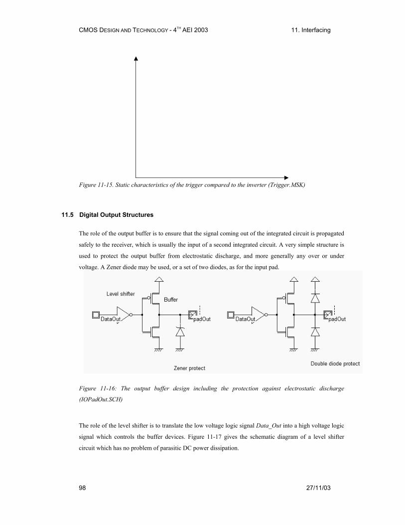
CMOS DESIGN AND TECHNOLOGY - 4TH AEI 2003 11. Interfacing
98 27/11/03
Figure 11-15. Static characteristics of the trigger compared to the inverter (Trigger.MSK)
11.5 Digital Output Structures
The role of the output buffer is to ensure that the signal coming out of the integrated circuit is propagated
safely to the receiver, which is usually the input of a second integrated circuit. A very simple structure is
used to protect the output buffer from electrostatic discharge, and more generally any over or under
voltage. A Zener diode may be used, or a set of two diodes, as for the input pad.
Figure 11-16: The output buffer design including the protection against electrostatic discharge
(IOPadOut.SCH)
The role of the level shifter is to translate the low voltage logic signal Data_Out into a high voltage logic
signal which controls the buffer devices. Figure 11-17 gives the schematic diagram of a level shifter
circuit which has no problem of parasitic DC power dissipation.
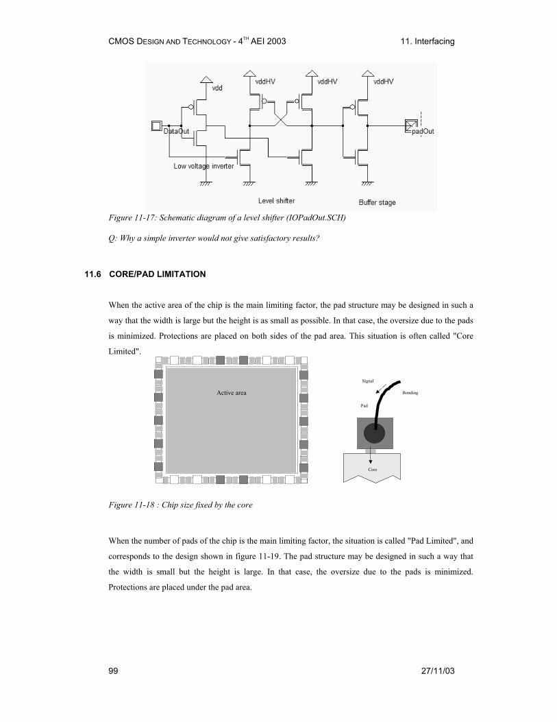
CMOS DESIGN AND TECHNOLOGY - 4TH AEI 2003 11. Interfacing
99 27/11/03
Figure 11-17: Schematic diagram of a level shifter (IOPadOut.SCH)
Q: Why a simple inverter would not give satisfactory results?
11.6 CORE/PAD LIMITATION
When the active area of the chip is the main limiting factor, the pad structure may be designed in such a
way that the width is large but the height is as small as possible. In that case, the oversize due to the pads
is minimized. Protections are placed on both sides of the pad area. This situation is often called "Core
Limited".
Active area
Core
Pad
Bonding
Signal
Figure 11-18 : Chip size fixed by the core
When the number of pads of the chip is the main limiting factor, the situation is called "Pad Limited", and
corresponds to the design shown in figure 11-19. The pad structure may be designed in such a way that
the width is small but the height is large. In that case, the oversize due to the pads is minimized.
Protections are placed under the pad area.
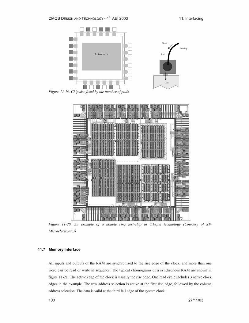
CMOS DESIGN AND TECHNOLOGY - 4TH AEI 2003 11. Interfacing
100 27/11/03
Active area
Core
Pad
Bonding
Signal
Figure 11-19. Chip size fixed by the number of pads
Figure 11-20. An example of a double ring test-chip in 0.18µm technology (Courtesy of ST-
Microelectronics)
11.7 Memory Interface
All inputs and outputs of the RAM are synchronized to the rise edge of the clock, and more than one
word can be read or write in sequence. The typical chronograms of a synchronous RAM are shown in
figure 11-21. The active edge of the clock is usually the rise edge. One read cycle includes 3 active clock
edges in the example. The row address selection is active at the first rise edge, followed by the column
address selection. The data is valid at the third fall edge of the system clock.
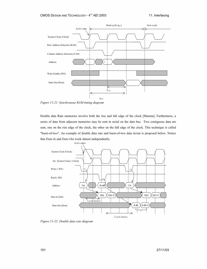
CMOS DESIGN AND TECHNOLOGY - 4TH AEI 2003 11. Interfacing
101 27/11/03
Address
Row Address Selection (RAS)
Column Address Selection (CAS)
Write Enable (WE)
Data Out (Dout)
Read cycle (tRC)
tRAC
tCAC
Active edge
System Clock (Clock)
l
New cycle
Figure 11-21: Synchronous RAM timing diagram
Double data Rate memories involve both the rise and fall edge of the clock [Sharma]. Furthermore, a
series of data from adjacent memories may be sent in serial on the data bus. Two contiguous data are
sent, one on the rise edge of the clock, the other on the fall edge of the clock. This technique is called
"burst-of-two". An example of double data rate and burst-of-two data in/out is proposed below. Notice
that Data In and Data Out work almost independently.
Address
Write (~WE)
Read (~RE)
Data In (Din)
Data Out (Dout)
Active edges
System Clock (Clock)
Inv. System Clock (~Clock)
Ain Bout Cin
D(A) D(A+1)
Q (B) Q (B+1)
D(C) D(C+1)
2 cycle latency
1 cycle latency
Figure 11-22: Double data rate diagram

CMOS DESIGN AND TECHNOLOGY - 4TH AEI 2003 12. References
102 27/11/03
[1]R.J Bakcer, H. W.Li, D. E. Boyce "CMOS design, layout and simulation", IEEE Press, 1998, www.ieee.org
[2] M. John, S. Smidth, "Application Specific Integrated Circuits", Addison Wesley, 1997, ISBN 0-201-50022-1,
www.awl.com/cseng
[3] B. Razavi "Design of Analog CMOS integrated circuits", McGraw Hill, ISBN 0-07-238032-2, 2001,
www.mhhe.com [4] Y. P. Tsividis "Operating and Modeling of the MOS transistor", McGraw-Hill, 1987, ISBN 0-07-065381-X
[5] S. M Sze "Physics of Semiconductor devices", John-Wiley, 1981, ISBN 0-471-05661-8
[6] Y. Cheng, C. Hu "MOSFET Modeling & BSIM3 user's guide", Kluwer Academic Publishers, 1999
[7] A. Hastings "The Art of Analog Layout", Prentice-Hall, 2001, ISBN 0-13-087061-7
[8] N. Weste, K. Eshraghian "Principles of CMOS VLSI design", Addison Wesley, ISBN 0-201-53376-6, 1993
[9] K. Lee, M. Shur, T.A Fjeldly, T. Ytterdal "Semiconductor Device Modeling for VLIS", Prentice Hall, 1993, ISBN
0-13-805656-0
[10] W. Liu "Mosfet Models for SPICE simulation including Bsim3v3 and BSIM4", Wiley & Sons, 2001, ISBN 0-471-
39697-4
[11] C. Motchenbacher, J. A. Connely "Low Noise Electronic System Design", Wiley & sons, 1993, ISBN 0-471-
57742-1
[12]A.K. Sharma "Semiconductor Memories", IEEE Press, 1996, ISBN 0-7803-1000-4
12 References


![Tutorial_Manual Microwind 1.d[1]](https://img.pdfslide.us/doc/110x75/5540d36d4a7959f00c8b4b0f/tutorialmanual-microwind-1d1.jpg)