Embed Size (px)
Citation preview

Northwestern University Mechanical Engineering Department
ME 381 - Introduction to MEMS Professor Horacio Espinosa
Three-Dimensional Dielectrophoresis Device with Integrated Actuating and Impedance Sensing
Michael Beltran
Robert Lam Bryan Lochman
December 9, 2007

2
Table of Contents ABSTRACT .................................................................................................................................................................3 INTRODUCTION .......................................................................................................................................................4 THEORY......................................................................................................................................................................5
DEP BACKGROUND ...................................................................................................................................................5 DEP CAGES AND ACTUATION ...................................................................................................................................9 IMPEDANCE SENSING...............................................................................................................................................10
SIMILAR DEP DEVICES........................................................................................................................................12 CMOS CHIP FOR INDIVIDUAL CELL MANIPULATION ................................................................................................12 A DIELECTROPHORETIC CHIP WITH A 3-D ELECTRIC FIELD GRADIENT ..................................................................13 MEMS ELECTROSTATIC PARTICLE TRANSPORTATION SYSTEM................................................................................14
FABRICATION METHODS ...................................................................................................................................14 RESULTS...................................................................................................................................................................16
PARASITIC CAGES....................................................................................................................................................16 CONCENTRATION INCREASES WITH MICROBEADS ...................................................................................................18 COMPARISON TO VOLTAGE SIMULATION RESULTS .................................................................................................18
RECOMMENDATIONS ..........................................................................................................................................20 REMOVAL OF PARASITIC CAGES..............................................................................................................................20 MANUFACTURING OF A MICRO SCALE DEVICE .......................................................................................................20 CREATE AN ARRAY OF DEVICES WITH A COMMON RESERVOIR .................................................................................24
CONCLUSIONS........................................................................................................................................................25 REFERENCES ..........................................................................................................................................................26 BIOGRAPHIES.........................................................................................................................................................27

3
Abstract Lab on a chip technology is the next generation of laboratory processes, which will allow the reduction in size of complex experimental setups to the size of a thumb. The lab on a chip device we are reviewing utilizes electronic manipulation and detection of microorganisms through a combination of dielectrophoresis (DEP) and impedance sensing. The reviewed device utilizes printed PCB board as the basis for electronic manipulation of polystyrene microbeads in close agreement with CAD simulations. The experiments were successfully repeated using S. Cerevisiae yeast cells, proving the effectiveness of DEP for particle manipulation and the ability of impedance sensing to eliminate optical and chemical detection methods. We then propose the further development of this technology to the microscale, outlining a manufacturing procedure using MEMS techniques such as lithography and chemical etching to allow for large scale production of devices in a silicon wafer array

4
Introduction Many chemical, biological, and medical fields currently consist of an incomprehensible number
of various tests, experiments and processes which can be characterized by their need for
integration of complex protocols and use of complex equipment. Lab-on-a-Chip architecture
seeks to scale down these individual processes to the size of conventional computer chips to
simplify the experimental process by integrating all necessary functions into one local device. By
integrating the functions of sensing, processing, and actuation into a compact package, the large
and complex devices that plague macro-scale techniques can be eliminated, thus limiting human
interaction with the experiment and simplifying the overall procedures. In addition to the
reduction in procedural steps, experiments previously limited to a laboratory environment can be
moved to new areas, allowing for on-site testing for many experiments which today require huge
lead times. In the future, this may allow for on site analysis for tests such as DNA matching,
food quality testing, and even water contamination, shortening the time required for these critical
experiments.
Many of these Lab-on-a-Chip devices require the manipulation of chemicals or particles,
requiring new and novel methods of controlling these items at the micro-scale. In particular, the
manipulation of particles and cells is of particular interest, as they respond to unique properties
absent in pure fluids and gasses. Dielectrophoresis (DEP) is a property which has been
extensively exploited in the manipulation of cells, whereby a particle may respond to a changing
electrical field due to an inherent polarization, whereby the particle may overall have a neutral
charge, but charges may be separated within the particle. Positive DEP (pDEP) is the situation
where a particle experiences a net force directed to locations with an increasing electric field
intensity, whereby negative DEP (nDEP) is the method whereby a particles is attracted to
decreasing field intensity. Problems arise with the use of pDEP and nDEP with the adhesion of
particles to walls. Since the maxima of an electric field cannot be established away from the
electrode, particles will tend to adhere to the electrode surface. With nDEP, in confined areas,
particles may also be forced far enough away from an electrode to come in contact with walls.
However nDEP provides a possibility for a particle to come into equilibrium with the force of
gravity, allowing for possible levitation within a medium.

5
Within Lab-on-a-Chip devices, sensing methods typically associated with particle or cellular
manipulation have been optical, involving fluorescent labeling in conjunction or separate from
optical techniques. Unfortunately these methods negate the benefits of Lab-on-a-Chip
architecture, usually requiring large instruments far above the size of the original chip.
Additionally, there are typically an increased amount of steps necessary to prepare the sample to
allow for optical detection.
Operation of stand alone devices such as Lab-on-a-Chip requires, at a minimum, a form of
feedback to allow the system to self-operate and correct. In many existing Lab-on-a-Chip
designs, the sensing system is entirely separate from the actuation apparatus. While this may not
be a problem with the operation of the device, there is an increase in the fabrication required to
create the entire system. Two separate systems must exist, each to accomplish only one task. It is
desired that a minimum amount of fabrication be required, since this is the largest contributor to
overall Lab-on-a-Chip cost.
We are proposing a device which addresses all of the previously stated problems, utilizing a form
of nDEP to prevent particle adhesion with a sensing method other than optical means, which may
be integrated with the existing actuation system. nDEP may be manipulated to create DEP
“cages” which allow particles to be encased within a virtual tube created by various electrodes
placed within a chamber. The particle detection system will no longer use optical means, but
electrical impedance, as particles will interfere with electrical flow between the same electrodes
creating the DEP cages. As described, the sensing method will be integrated into the electrodes
responsible for actuation, reducing the necessary fabrication for the device. Combining these
processes on the chip will enable the automation of sensing and actuation, essentially eliminating
the need for human interaction within the system. Actuation can then be controlled by the
sensing feedback, entirely contained within the chip architecture.
Theory
DEP Background Dielectrophoresis (DEP) is a method of moving neutral particles within a non-uniform electric
field. By placing electrodes in a particular asymmetric conformation, a gradient for an electric

6
field can be generated, which can create an electric dipole within neutral particles (in our case, a
cell). Due to this phenomenon, cells can experience a net force directed towards increasing or
decreasing field intensity, depending on the design of the chip. Extending this concept to 3D, a
DEP cage can be created in order to trap particles, which is extremely useful in several areas of
biotechnology, namely in electro-manipulation, focusing, characterization and detection.
The governing equation for a DEP-induced force upon a spherical particle is: Equation 1: DEP-Induced Force
23 ]Re[2 EKrF m ∇= επ
where r is the radius, E is the nonuniform electric field, εm is the permittivity of the liquid
medium and Re[K] is the Clausius-Mossotti factor. Note that Equation 2: Clausius-Mossotti Factor
**
**
2 mp
mpKεεεε
+
−=
where εp is the permittivity of the particle.
The DEP-induced force can be negative or positive, giving it the capability to direct particles
towards high electric field regions (positive DEP) or towards low electric fields (negative DEP).
This phenomena is partially dependent on the linear relationship between the force and the
polarizability relationship of the medium and particle (Re[K]). In other words, particles with a
greater polarizability than the surrounding medium exhibit positive DEP relationships while
particles with lower polarizability than the medium will react in the opposite manner. This
ability allows us to concentrate similar particles or separate different particles.
In addition, the complex permittivity of the medium (ε*) is a function of the applied electric field
frequency: Equation 3: Permittivity of the Medium
ωσεε j−=*
where σ is the conductivity and ω is the angle frequency of the electric field. Using Equation
3and Equation 2, at low frequencies the Clausius-Mossotti factor can be approximated as

7
Equation 4: Clausius-Mossotti Factor at Low Frequencies
mp
mpKσσσσ2+
−≈
At high frequencies the Clausius-Mossotti factor can be approximated as
Equation 5: Clausius-Mossotti Factor at High Frequencies
mp
mpKεεεε2+−
≈
At different frequencies, the polarization factor can be switched between positive and negative a
value, allowing another control factor over positive of negative DEP force.
These DEP concepts can be extended to 3-D, where electric fields varyingly extend into the
vertical axis.
When considering vertical forces, the buoyancy force (FB) of the particles must be accounted for
as well: Equation 6: Buoyancy Force
( )grF mpB ρρπ −= 3
34
where r is the radius of the particle and ρp and ρg are the densities of the particle and medium,
respectively.
The buoyancy force can act with or against the vertical DEP force, depending on the orientation.
At a certain point between two electrodes, the vertical DEP force and buoyancy force will be in
equilibrium, allowing particles to suspend in the solution above the surface.
Figure 1: Balancing Buoyancy and DEP Forces [5]
Balancing the DEP and buoyancy forces:
8
Equation 7: Balancing the DEP and Buoyancy Forces ( )
m
mp gEK
ερρ
32
]Re[ 2 −=∇
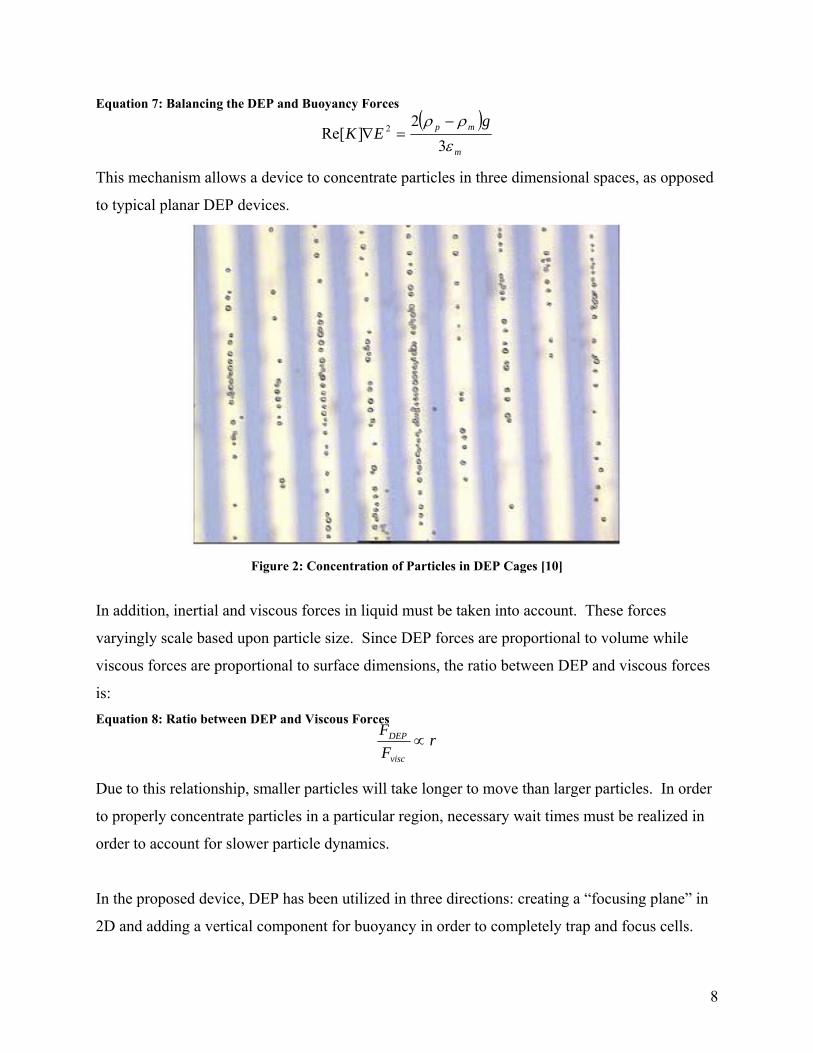
This mechanism allows a device to concentrate particles in three dimensional spaces, as opposed
to typical planar DEP devices.
Figure 2: Concentration of Particles in DEP Cages [10]
In addition, inertial and viscous forces in liquid must be taken into account. These forces
varyingly scale based upon particle size. Since DEP forces are proportional to volume while
viscous forces are proportional to surface dimensions, the ratio between DEP and viscous forces
is: Equation 8: Ratio between DEP and Viscous Forces
rFF
visc
DEP ∝
Due to this relationship, smaller particles will take longer to move than larger particles. In order
to properly concentrate particles in a particular region, necessary wait times must be realized in
order to account for slower particle dynamics.
In the proposed device, DEP has been utilized in three directions: creating a “focusing plane” in
2D and adding a vertical component for buoyancy in order to completely trap and focus cells.

9
DEP Cages and Actuation The actuation of the electrodes on the bottom of the chip is responsible for DEP cage movement.
DEP-induced forces will move particles towards the target electrode in order to increase the
concentration of the matter being analyzed at that particular target electrode. The DEP cage is
able to move towards the center of the chip by applying a counter-phase signal across the entire
top plate of the chip while applying alternating in-phase and counter-phase signals to the bottom
electrodes. The pattern on the bottom electrode, as seen in Figure 3, is an in-phase electrode
bounded by out of phase electrodes, then moved towards the target electrode as in Figure 4
Figure 3: Formation and Actuation of DEP Cages [1]
Figure 4: Actuation of DEP Cages Towards Target Electrode [1]

10
The time it takes to shift the DEP cage from one electrode to the next depends on the particle
size. Upon an immediate cage shift, particles will remain still due to inertial and viscous forces,
but will then move to the center of the shifted cage due to their vicinity within the attraction
basin of the shifted cage. The time it takes for these particles to move to the center of the shifted
cage determines the time period of actuation for the DEP cages.
Due to the aforementioned relationship between DEP and viscous forces, Equation 8, large
particles move quicker to shifted DEP cages (for a particle with a diameter of 50μm travel time is
approximately 2s) while smaller particles move slower (for a particle with a diameter of 3μm
travel time is between 5-10s). The time period between shifting cages between electrodes must
be chosen such that the smallest particles will not be left behind.
Impedance Sensing To determine the concentration of particles in the DEP cages, impedance sensing is performed
between the shifting of the DEP cages. This is done by connecting the measuring electrode to a
transimpedance amplifier and connecting the rest of the electrodes to ground while still
continuing to have the top plate connected to a counter-phase signal, seen in Figure 5.
Figure 5: Impedance Sensing [1]
During sensing, DEP cages are switched off. Since the time it takes for particles to fall to the
bottom of the chamber (≈1s for the smallest particle) is much longer than the time it takes for
impedance sensing to take place (≈10ms) particles will continue to levitate during sensing.

11
This transimpedance amplifier contains a capacitor with known capacitance, CF, and a Resistor
with known Resistance, RF. The particles between the electrode and top plate will create a
change in capacitance and resistance which can be sensed and correlated to the quantity of
particles between the electrode and top plate. The transfer function for the sensing circuit was
discovered through circuit analysis and is displayed in Equation 9 where Vo is the output voltage,
Vi is the input voltage, RF and CF are the feedback resistance and capacitance, and RM and CM
are the resistance and capacitance between the electrode and lid. Equation 9: Transfer Function for Sensing Circuit
⎟⎟⎠
⎞⎜⎜⎝
⎛++
−=FF
MM
M
F
i
o
CjwRCjwR
RR
jwVV
11
)(
At lower frequencies ( )/(1 MM CRw << and )/(1 FF CRw << ) the resistance effects will dominate
the system and Equation 9 can be reduced to Equation 10. Equation 10: Sensing Equation at Low Frequencies
M
F
i
o
RR
VV
−=
At higher frequencies ( )/(1 MM CRw >> and )/(1 FF CRw >> ) the capacitive effects will dominate
the system and Equation 9 can be reduced to Equation 11. Equation 11: Sensing Equation at Higher Frequencies
F
M
i
o
CC
VV
−=
Equation 4 illustrates that using a low frequency input stimulus will trap a particle if its
conductivity is lower than the medium’s, leading to a decrease in conductivity between the
electrode and the lid. If the same frequency is used for both activating the DEP cages and
sensing then RM will increase with the inclusion of trapped particles: Equation 12: Effect of Particles on Resistance at Low Frequencies
wopM
wpM RR >
where wpMR is the system with particles and wop
MR is the system without particles. Using Equation
10 and 12, it can be seen that output voltage amplitude of the amplifier will decrease with
trapped particles.

12
Equation 5 demonstrates that using a high frequency input stimulus will trap a particle if its
permittivity is lower than the medium’s. If the same frequency is used for activating the DEP
cages and sensing then: Equation 13: Effect of Particles on Capacitance at High Frequencies
wopM
wpM CC <
Using Equation 11 and 13 it can also be seen that the output voltage amplitude will decrease with
trapped particles.
A correlation can then be created between the amount of particles and the output voltage at both
the low and high frequencies. This will allow for detection of particles by observing the output
voltage of the system.
Similar DEP Devices
CMOS Chip for Individual Cell Manipulation
Figure 6: CMOS Chip [6]
Using CMOS technology, this device was fabricated with 102,400 actuation electrodes, in a
320x320 array within a 8 x 8 mm2 chip. Each electrode is 20 µm x 20 µm. This device allows
the selection and manipulation of single cells. This device demonstrates the capability to
manipulate up to 10,000 cells in parallel, which has potential in drug screening, cell separation
and analysis. Instead of using capacitive sensing techniques, the authors propose an integrated
method using optics.

13
A Dielectrophoretic Chip with a 3-D Electric Field Gradient
Figure 7: DEP Chip with a 3D Electric Field Gradient [2]
In this device, the authors created an asymmetric 3D electric gradient through specially
configured electrodes. Thick electrodes are integrated with vertical wall structures while thin
planar electrodes are placed on the bottom layer substrate. This configuration achieves an
enhanced vertical DEP force, allowing the device to run at lower voltages and temperatures.

14
MEMS Electrostatic Particle Transportation System
Figure 8: MEMS Electrostatic Transportation System [7]
The authors here were able to construct an electrostatic device capable of transporting particles
5-10µm in diameter in air. They were able to demonstrate a relationship between particle
transportation efficiency with insulator film thickness. Surface modification treatments were
performed in order to reduce adhesive forces.
Fabrication Methods The fabrication of this DEP Lab-on-a-Chip does not involve any MEMS construction techniques.
(Scaling down this device with MEMS techniques is discussed further in the Recommendations
section). The reviewed chip consists of a PCB board, gold electrodes, optic fiber spacers, a
gasket and a transparent conductive lid. The base is a printed circuit board (PCB) that contains
strips of gold electrodes that were attached during the fabrication of the board. The most
common form for attaching electrodes to a PCB board is by silk screening the pattern onto a gold

15
clad board and then etching and removing the screened resist. The PCB board is separated from
the conductive lid through the use of optic fibers, which determines the device’s height, while a
gasket seals the microchamber. The lid is connected to the PCB device by using conductive
glue. The device is shown in Figure 9 along with representations of DEP cages. Advantages for
not using MEMS techniques include the possibility of having larger microchambers, decreased
production costs and turnaround time.
Figure 9: Sketch of the Device [1]

16
Results
Parasitic Cages One of the major problems that occur with this device is the formation of parasitic cages. These
parasitic cages, represented as a dark spot between electrodes 3 and 4 in Figure 10a, are formed
when a counter-phase signal is applied to one of the three electrodes, electrode 2 in Figure 10a,
while an in-phase single is applied to the other two electrodes, electrodes 3 and 4 in Figure 10a.
A parasitic nDEP cage will appear in between the two in-phase electrodes because this spot
corresponds to an electric field minimum.
Figure 10: (a)Parasitic nDEP Cage (b) Shifted DEP cage [1]
Particles are injected into the microchamber in a random fashion, , causing some to be trapped in
parasitic cages after the device is activated because they are in the attraction basin of these cages.
Particles in the parasitic cages can be recovered by shifting the DEP cage as seen in Figure 10b.
Particles trapped in the original parasitic cage will now be attracted to the cage above electrode
3, but a new parasitic cage will form, attracting smaller particles from the original DEP cage due
to their inherently slower movement through fluid.

17
Two methods were found to reduce the effect of parasitic cages. The first was to add an
intermediate step while shifting the DEP cage, seen in Figure 11. During this step the particles
are attracted to a DEP cage between the starting and ending electrodes. Although some particles
are still trapped in a parasitic cage below the DEP cage, the majority will be recovered in the
final step.
Figure 11: Intermediate Step in DEP Cage Shift [1]
Another way to reduce the effect of parasitic cages is to minimize the gap between electrodes,
seen in Figure 12. This will both minimize the attraction basin of a parasitic cage and only allow
for the entrapping of similar sized particles, possible eliminating all particles trapped. This kind
of spacing is only possible using MEMS fabrication techniques, instead of the PCB techniques
used to make this device.
Figure 12: Minimized Gap between Electrodes affect on Parasitic Cages [1]

18
Concentration Increases with Microbeads A time evolution of device is shown in Figure 4. In a), the device and DEP are turned off with
the microbeads scattered at the bottom of the microchamber. Upon activation, DEP cages form
above specified electrodes in b). Figures c) through e) show DEP cages being manipulated by
being merged into each other, effectively increasing the concentration of particles in a chosen
area.
In this experiment, microbeads of 3.46 µm diameter are suspended in distilled waters.
Electrodes are driven at 100 kHz 10 Vpp. In the diagram shown in Figure 4, the concentration of
the microbeads is continually being driven towards the center, forming one large concentration.
One could potentially merge DEP cages at several points depending on the electrode
configuration.
Comparison to Voltage Simulation Results Microbead experiments result in the formation of a cage with a distribution of particles far too
complex to be modeled at the level of individual particles, as this would require the integration
of a time factor and dilution equations in conjunction with DEP forces. However, in our case, the
microbead diameter (3.46 μm) is much less than the diameter of the DEP cage (100μm). This
allows the following assumptions:
• Particle cloud within the DEP cage can be modeled as homogenous
• Permittivity and Conductivity depend solely on the ratio between the volume of
microbeads and suspending medium in the cylinder (distilled water).
With these assumptions, it is possible to simulate the electric field using FEMLAB in a 2-D
perspective, corresponding to a cross section of the device with circular cross section cages. An
electric field simulation is performed to calculate the resistance without particles, followed by
four simulations to calculate the Rmwp, for each of the concentration steps. The initial radius of
the cylinder is determined by fitting the sensing output to the Rmwp value. Thus, if Vol0 and r0 are
the initial cylinder volume and radius, merging n cages the volume becomes Voln = n*r0 and rn =
n1/2 *r0. Figure 13 shows the correlation between measured and simulated results, displaying a
strong correlation with a starting radius of 25 μm, fitting with optically determined
measurements.

19
Figure 13: Comparison between simulated and measured output amplitude for the central electrode for
3.46μm polystyrene microbeads in distilled water (σ = 0.5μs/cm, stimulus: 10V at 100 kHz). For the simulations a unit volume of V= πr0
2 has been used, where r0= 25μm, L= 1cm [1]
The experiments were verified by repetition using S. cerevisia, a bakers yeast that has been
grown at 25°C in a Sabaroud medium (Oxoid). ). The yeasts have been grown for 48 hours,
harvested by centrifugation, washed twice with 25mL of physiological solution (0.9% NaCl) and
once in 25mL of a 280-mM mannitol solution. The dielectrophoretic behavior of S. cerevisiae
cells suspended in 280-mM mannitol at a changing frequency has been analyzed in the proposed
device by microscopic observation. Mannitol solution is used instead of the normal physiological
solution to reduce conductivity within the device, while preserving osmotic pressure. An increase
in conductivity would lead to heating of the buffer solution, in addition to the shielding of the
electric field by ions in the solution. Tests of S. cerevisia in the intended frequency range (30
kHz–1 MHz), displays a pDEP behavior in frequencies above 200 kHz. Thus, a 100 kHz
frequency will be used to allow nDEP behavior to trap the yeasts in the DEP cages. Frequencies
lower than 30 kHz has been avoided to prevent electrolysis. The same procedure is used for S.
cerevisiae as with the microbeads: The device is filled with a suspension of S. cerevisiae in 280-
mM mannitol. The electrodes are energized with 100 kHz frequency with 10V amplitude. The
concentration cycle is repeated 5 times, increasing the concentration in the central cage by a
factor of 9. Sensing values measured after each concentration cycle is displayed in Figure 14.

20
Figure 14: Measured output amplitude for the central electrode as a function of the number of merged cages
for S. cerevisia in 280-mM mannitol solution. (σ=0.5μs/cm, stimulus: 10V at 100 kHz) [1]
Recommendations
Removal of Parasitic Cages In order to remove unwanted parasitic cages from the bottom of a microchamber, we propose to
embed electrodes into the substrate via ion implantation.
Manufacturing of a Micro Scale Device The device as so far described has been at a rather large scale, with the device reservoir thickness
at 250μm, and the electrode spacing at size at 200μm. While this is sufficient for a device with
only a few electrodes, any device requiring more than 3 electrodes will range above 1mm in size.
We thus propose a scaling of the device by an order of magnitude, whereby electrode size and
spacing is only 20μm, and reservoir thickness is reduced to only 50μm. Size is limited by both
the properties of DEP, and the particle size to be used. There exist many papers [2,3] indicating
that DEP can still be used at this scale, so scale has been chosen to allow for the manipulation of
cells, which at most can be 10μm in diameter. With 20μm spacing, cages can at most be 40μm in
diameter, allowing for a reasonable amount of the largest cells to be trapped. With the reduction

21
in size, it is thus possible to have an array of 100 electrodes on a device measuring only slightly
larger than 4mm
Our proposed device will be constructed with three separate wafers; A base layer containing
electrodes, central layer to make up the fluid reservoir, and a top transparent conductive layer to
allow observation as well as include fluid channels to fill each device. Listed below is a sequence
outlining device construction. Cross sectional view is on the left, top view on the right.
Key:
Base Wafer:
Step 1: Base layer consisting of silicon wafer base, with layer of silicon oxide and photoresist.
Step 2: Mask pattern inverted from intended electrode pattern.
Step 3: Removal of Photoresist
Step 4: Dry Plasma etching removal of silicon oxide
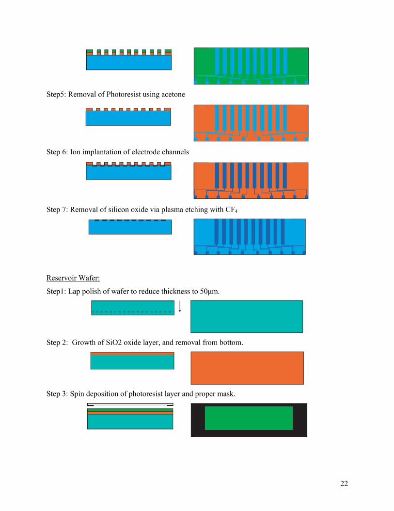
22
Step5: Removal of Photoresist using acetone
Step 6: Ion implantation of electrode channels
Step 7: Removal of silicon oxide via plasma etching with CF4
Reservoir Wafer:
Step1: Lap polish of wafer to reduce thickness to 50μm.
Step 2: Growth of SiO2 oxide layer, and removal from bottom.
Step 3: Spin deposition of photoresist layer and proper mask.

23
Step 4: Exposure to light and removal of photoresist.
Step 5: Dry plasma etching of silicon oxide.
Step 6: Removal of photoresist using acetone.
Step 7: KOH etching of silicon wafer.
Step 8: Removal of silicon oxide via plasma etching with CF4
Alignment and Assembly
Step 1: Wafer alignment and bonding of base to reservoir layer, allowing access to electrodes.

24
Create an array of devices with a common reservoir
With the reduction in size of the device, we are proposing the creation of an array of DEP cage
devices, linked together by a single central reservoir. Since manual filling of a new device would
be extremely difficult given its size, linking an array of devices to a larger reservoir would allow
filling of multiple devices at once. The advantages of an array of devices also allows for larger
scale operations. With individual control of each device, a sample containing many different
particles and respective concentrations can be routed to a large number of devices. At each of
these locations, the proper frequencies and amplitudes can be selected to provide selective
concentration increases of a particular particle of interest. Thus, rapid experiments can be
conducted to either separate known particles, or identify particle makeup based on input values
corresponding to certain particles. The device array we propose would be constructed in a
manner similar to Figure 15.
Figure 15: Proposed array layout of 24 DEP cage devices with a common central reservoir
The top sealing layer can incorporate this microchannel pattern, allowing each channel to empty
into the device reservoir. The central reservoir can be a simple hole in the sealing layer, and the
microchannels can be fabricated using conventional micromilling. The layer can thus be placed

25
with microchannels on the bottom to seal the devices and microchannels against the silicon
wafer.
Conclusions The utilization of engineering tools and techniques towards addressing primary biomedical
problems, i.e. concentrating particles within a sample for biodetection, providing a novel view
into the integrative nature of this course. Concepts involving Lab-on-a-Chip design principles,
DEP actuation and impedance sensing provide an encompassing review for microfabrication
techniques. In particular, we delved into an in depth review in device construction and DEP
principles and results. Accomplishing our primary goal, we provided a step-by-step protocol and
an explanation of design choices chosen by the author in fabricating this device. In addition, the
physical principles that drove the device were examined in detail. Lastly, we were able to begin
a discussion on where this technology is heading and possible improvements that can be made in
the future.

26
References 1 Medoro, G.; Manaresi, N.; Leonardi, A.; Altomare, L.; Tartagni, M.; Guerrieri, R. A
Lab-on-a-Chip for Cell Detection and Manipulation. IEEE Sensors Journal, 2003, 3, 317-325
2 Iliescu, C.; Yu, L.; Xu, G.; Tay, F. A Dielectrophoretic Chip With a 3-D Electric Field Gradient, Journal of Microelectromechanical Systems, 2006, 15, 1506-1513
3 Suehiro, J.; Pethig, R. The Dielectrophoretic Movement and Positioning of a Biological Cell Using a Three-Dimensional Grid Electrode, Journal of Physics D: Applied Physics, 1998, 31, 3298-3305
4 Zimmermann, U.; Friedrich, U.; Mussauer, H.; Gessner, P.; Hamel, K.; Sukhorukov, V. Electromanipulation of Mammalian Cells: Fundamentals and Application, IEEE Transactions on Plasma Science, 2000, 28, 72-82
5 Markx, G.; Pethig, R.; Rousselet, J. The dielectrophoretic levitation of latex beads, with reference to field-flow fractionation, Journal of Physics D: Applied Physics, 1997, 30, 2470-2477
6 Manaresi, N.; Romani, A.; Medoro, G.; Altomare, L.; Leonardi, A.; Tartagni, M.; Guerrieri, R. A CMOS Chip for Individual Cell Manipulation and Detection, IEEE Journal of Solid-State Circuits, 2003, 38, 12:2297-2305
7 Desai, A.; Lee, S-W.; Tai, Y. A MEMS Electrostatic Particle Transportation System. Sensors and Actuators, 1999, 73, 37-44
8 Jawitz, Martin W. Printed Circuit Board Materials Handbook. New York: McGraw-Hill Professional Book, 1997. p. 301-302
9 Plonus, Martin. Electronics and Communications for Scientists and Engineers. Boston: Academic P, 2001. 51-72.
10 Chen, D. F., H. Du, and W. H. Li. "Bioparticle Separation and Manipulation Using Dielectrophoresis." Sensors and Actuators A os 133 (2007): 329-334.

27
Biographies
Robert Lam received his Bachelor of Science degree from the University of California, Los Angeles (UCLA) in 2007 and is currently pursuing a Ph.D. degree in Mechanical Engineering at Northwestern University. He is a graduate student researcher in the Nanoscale Biotic-Abiotic System Engineering (N-BASE) Laboratory and is interested in the study of micro and nanoscale biological sciences.
Bryan Lochman will receive a Bachelor of Science degree in Mechanical Engineering from Northwestern University in June of 2008. His research interests include fluid dynamics and stress analysis. Michael Beltran graduated from the Massachusetts Institute of Technology in 2007 with a Bachelor of Science degree in Mechanical engineering. He is currently pursuing a Ph D. in Mechanical engineering at Northwestern University as a member of the Advanced Materials Processing Lab (AMPL). His research focuses on micromanufacturing and the expansion of desktop manufacturing technologies.