Embed Size (px)
Citation preview

1
A D D E N D U M
C
N O N - S I L I C O N D I G I T A L C I R C U I T S
C.1 Introduction
C.2 Digital Gallium Arsenide Design
C.2.1 GaAs Devices and Their Properties
C.2.2 GaAs Digital Circuit Design
C.3 Low-Temperature Digital Circuits *
C.3.1 Low-Temperature Silicon Digital Circuits
C.3.2 Superconducting Logic Circuits
C.4 Summary
C.5 To Probe Further
C.6 Exercises and Design Problems
n
Designing high speed logic in GaAs
Extreme performance using cryogenic techniques
2 Non-Silicon Digital
C.1 Introduction
This chapter deals with the design of digital integrated circuits with operating speeds inthe multiple hundreds of MHz, and even the GHz range. These speeds are desirable in thecore processors of super- and mainframe computers, and even high-end workstations.High performance is also a prime requirement in the domain of high-speed signal-acquisi-tion apparatus, such as digital sampling oscilloscopes. Measurement equipment mustalways be faster than the circuits it observes; hence the need for high-speed logic. With theadvent of optical fiber, digital communication systems have been extended into theGbits/sec area and need extremely high-speed front-end circuitry. Finally, the availabilityof high-speed technologies simplifies the task of automating the design process for high-performance circuits.
In our quest for these ever higher speeds, even bipolar designs eventually reach amaximum. When extreme performance is a necessity, room-temperature silicon isreplaced by other semiconductor materials such as gallium arsenide (GaAs). The lure ofGaAs and other compound semiconductors is a substantial increase in carrier mobilityand, hence, performance. An alternative solution is to opt for operation at a reduced tem-perature. Lowering the temperature reduces the delay of traditional semiconductor compo-nents. Some materials even have the property of becoming superconductive whenoperated below a certain temperature, which eliminates resistivity altogether. Circuitswith mind-boggling performance can be conceived using these technologies.
C.2 Digital Gallium Arsenide Design
The combination of the latest manufacturing technology and advanced circuit designmakes it possible to realize inverters with propagation delays of around 20 psec in siliconbipolar. Once again, treat this value with caution, as it is obtained in an ideal structuresuch as a ring oscillator (with a fan-out of 1). The actual gate delay that can be achieved inactual designs is at least twice as large, and more often many times higher. When fasterswitching speeds are required such as in the next generation of super-computers or in thefront-end of advanced radio-telecommunication devices, silicon-based designs run out ofsteam.
This does not mean that going faster is out of the question. Other semiconductormaterials, such as gallium arsenide (GaAs) and silicon-germanium (SiGe), have switchingproperties that exceed the performance of silicon. In the next sections, some attention isdevoted to the design of digital gates in these technologies. Although these approachesrepresent only a small fraction of the digital design market, it is valuable to have animpression of how digital design for very high speed is conducted. We will limit ourselvesto a discussion of GaAS-based design.
From the 1st Edition 3
C.2.1 GaAs Devices and Their Properties
GaAs Material Properties
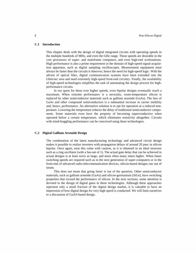
The performance of submicron silicon MOS devices is constrained by the maximum elec-tron-drift velocity υsat, which approximately equals 107 cm/sec. As this is an intrinsicproperty of the material, faster switching speeds can only be achieved by a scaling of thetechnology or by exploring other semiconductor materials. An example of the latter is gal-lium-arsenide, which is a compound semiconductor material that has the intrinsic capabil-ity of being approximately twice as fast as silicon. Figure C.1 plots the carrier velocity of
electrons and holes in both GaAs and Si as a function of the electrical field. For lower fieldstrengths, the velocity is proportional to the field for all carriers. For higher field values,the carrier velocity saturates to approximately 107 cm/sec, independent of the material orthe carrier. The most important lesson to be learned from this graph is that at lower valuesof the electrical field, GaAs electrons display a higher velocity, peaking at 2 × 107 cm/secbefore dropping to the saturation value. The velocity increase is due to the lower effectivemass me of the GaAs electrons compared to Si. When operated at low electrical fields,GaAs has the capability of being substantially faster than Si. A number of the importantproperties of GaAs are enumerated below.
• When operated at low electrical fields, n-type GaAs circuits can be twice as fast assilicon circuits. To exploit this feature requires operation at low voltages (around1 V).
• This difference becomes even more significant for light doping levels, where theelectron mobility can reach 8000 to 9000 cm2/Vsec at room temperature. This isapproximately 10–20 times higher than silicon. Special devices such as the HEMT(high electron mobility transistor) have been developed to exploit this feature.These structures produce some of the fastest logic available, especially at lower tem-peratures.
Figure C.1 Measured carrier velocity versus electric field for Si and GaAs [Sze69].
4 Non-Silicon Digital
• Unfortunately, holes in GaAs do not exhibit equally desirable properties. The holevelocity is approximately 15–20 times lower compared to the GaAs electron. Thismeans that the complimentary structures are not as desirable in GaAs as they werein Si.
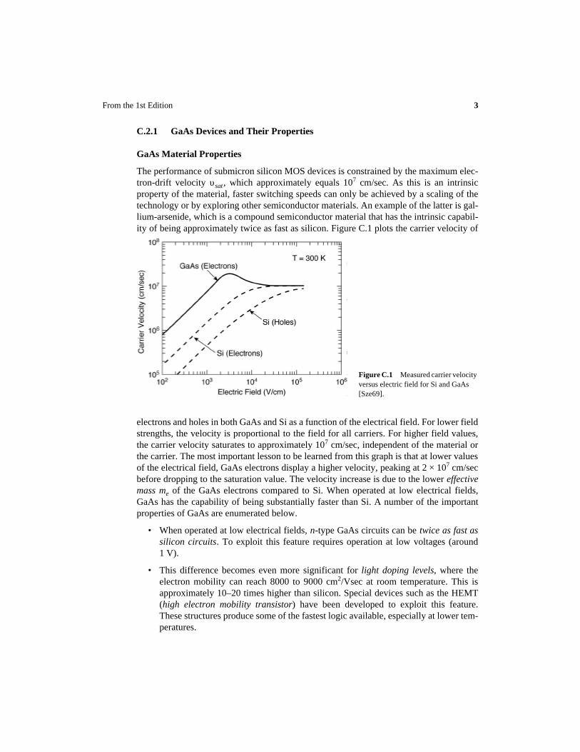
• Due to very high levels of surface-state charge, structures like metal-oxide-semicon-ductor transistors are not possible. Most GaAs designs, therefore, make use ofMESFET (metal-semiconductor field-effect transistor) devices, which are intro-duced in the next section.
• Pure GaAs is semi-insulating with a resistivity between 107 and 109 Ω·cm at roomtemperature. This means that devices made of doped GaAs can be isolated fromeach other by the insertion of undoped material, although additional isolation can beprovided by selective ion implantation. This is more area-effective than the field-oxide approach in CMOS. It also has the advantage of reducing the parasiticcapacitance.
• Due to a larger band-gap and the semi-insulating substrate, GaAs has the advantageof being more immune to radiation effects. It is therefore attractive for space andmilitary applications where it is in direct competition with silicon-on-insulatortechnologies.
• Finally, but most importantly, GaAs is an extremely brittle and fragile material. Forthis particular reason, GaAs wafers tend to be no larger than three inches, whereassix-inch and larger silicon wafers are common. This results in a reduced manufac-turing efficiency. Moreover, getting a reasonable yield has been challenging due tothe high defect density in the basic material and the tight device requirements.
The MESFET Device
As mentioned previously, the lack of a MOS-style device has made the MESFET (metal-semiconductor FET) the device of choice in GaAs design. A cross-section of an n-MESFET is shown in Figure C.2. It consists of a conductive n-type surface channel with a
thickness T, located between two n+ ohmic contacts that act as source and drain. Semi-insulating GaAs is used as the substrate material. The device control terminal (the gate) isimplemented by depositing a metal (typically Ti/Pd/Au, although Al, W, and Pt alloyswork as well) on a section of the channel, so that a Schottky-barrier diode is created. ASchottky diode is a metal-semiconductor junction formed by depositing a small metal con-
Semi-insulating GaAs
SG
D
n n+n+
L
T
Figure C.2 Cross-section of a GaAs MESFET.
Channel
Depletion region
From the 1st Edition 5
tact onto a lightly doped n-type semiconductor. The resulting diode relies on single-carrierconduction, what results in fast switching times. Appendix D offers a more detailed dis-cussion of this device.
The principles of operation and the basic relationships governing the device are sim-ilar to those of the silicon-junction FETs (JFET) and MOSFETs. The MESFET is a uni-polar transistor, which means that conduction is dominated by one type of carrier, in thisparticular case the electron. Its operation is can be understood from the following qualita-tive analysis:
• Under zero-bias conditions (VGS = 0), a depletion region is created under the gatedue to the built-in voltage of the metal-semiconductor junction, as shown in FigureC.2. This reduces the number of mobile carriers present in the channel. Typically,the thickness of the depletion layer is smaller than T, which means the channel isstill conducting. The nominal MESFET transistor is therefore a depletion device.
• Applying a positive voltage to the gate reduces the width of the depletion layer. Thisincreases the conductivity of the channel. However, once the gate-channel voltage issufficiently high, the Schottky diode becomes forward-biased, and current startsflowing into the gate. As no further increase in conductivity occurs from that pointon, this condition is to be avoided in general. The voltage at which forward conduc-tion of the gate occurs depends upon the gate metal and ranges around 0.5–0.7 V.
• When the gate voltage is reduced, the depletion region extends, and the channel con-ductivity drops owing to the smaller cross-sectional area of the conducting channel.This trend continues until the depletion region extends through the conductive layer(or Wdepl > T) and pinches off the channel. At that point, the transistor is turned offas the channel conductivity drops to 0. The gate-source voltage needed to make thishappen is called the pinch-off voltage VP. The pinch-off voltage is analogous to thethreshold voltage in a MOS transistor and is a function of the thickness of the chan-nel, the doping level, and the built-in voltage of the Schottky diode. Typical valuesof VP for the depletion devices range from –0.7 V to –2.5 V.
As the depletion device is the generic MESFET GaAs transistor, it is tempting to buildlogic gates using only these devices, as was the case in the earlier days of GaAs digitaldesign. Unfortunately, such a design approach requires the availability of multiple supplyvoltages—the gate-source voltage has to be negative to turn the device off, while thedrain-source voltage has to be positive for conduction.
An enhancement device can be realized by either reducing the channel thickness orby ion implantation, ensuring that channel pinch-off is achieved under zero-bias condi-tions. The logic swing for an enhancement-based logic gate is limited to the differencebetween the pinch-off voltage, which normally ranges between 0 and 0.2 V, and the volt-age at which the Schottky-barrier diode begins to conduct (around 0.7 V). Under these lowswing conditions, small variations of the pinch-off voltage can have a dramatic impact onthe circuit’s functionality or performance. The realization of complex circuits, therefore,requires an accurate control of the channel thickness over the complete wafer to minimizepinch-off voltage variations.
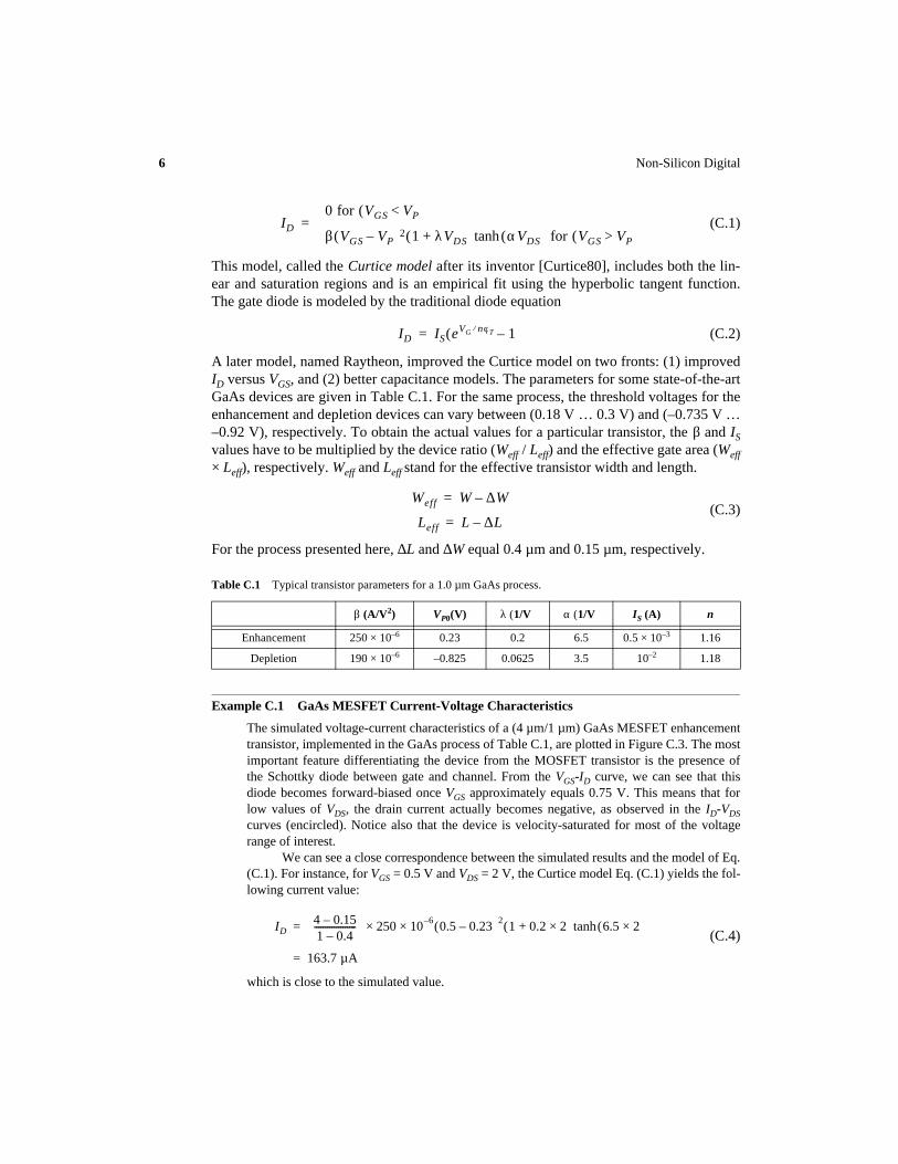
The device model for the GaAs MESFET is remarkably similar to the MOSFETone. An extra factor is included to incorporate the effects of velocity saturation.
6 Non-Silicon Digital
(C.1)
This model, called the Curtice model after its inventor [Curtice80], includes both the lin-ear and saturation regions and is an empirical fit using the hyperbolic tangent function.The gate diode is modeled by the traditional diode equation
(C.2)
A later model, named Raytheon, improved the Curtice model on two fronts: (1) improvedID versus VGS, and (2) better capacitance models. The parameters for some state-of-the-artGaAs devices are given in Table C.1. For the same process, the threshold voltages for theenhancement and depletion devices can vary between (0.18 V … 0.3 V) and (–0.735 V …–0.92 V), respectively. To obtain the actual values for a particular transistor, the β and ISvalues have to be multiplied by the device ratio (Weff / Leff) and the effective gate area (Weff× Leff), respectively. Weff and Leff stand for the effective transistor width and length.
(C.3)
For the process presented here, ∆L and ∆W equal 0.4 µm and 0.15 µm, respectively.
Example C.1 GaAs MESFET Current-Voltage Characteristics
The simulated voltage-current characteristics of a (4 µm/1 µm) GaAs MESFET enhancementtransistor, implemented in the GaAs process of Table C.1, are plotted in Figure C.3. The mostimportant feature differentiating the device from the MOSFET transistor is the presence ofthe Schottky diode between gate and channel. From the VGS-ID curve, we can see that thisdiode becomes forward-biased once VGS approximately equals 0.75 V. This means that forlow values of VDS, the drain current actually becomes negative, as observed in the ID-VDScurves (encircled). Notice also that the device is velocity-saturated for most of the voltagerange of interest.
We can see a close correspondence between the simulated results and the model of Eq.(C.1). For instance, for VGS = 0.5 V and VDS = 2 V, the Curtice model Eq. (C.1) yields the fol-lowing current value:
(C.4)
which is close to the simulated value.
Table C.1 Typical transistor parameters for a 1.0 µm GaAs process.
β (A/V2) VP0(V) λ (1/V) α (1/V) IS (A) n
Enhancement 250 × 10–6 0.23 0.2 6.5 0.5 × 10⁻³ 1.16
Depletion 190 × 10–6 –0.825 0.0625 3.5 10–2 1.18
ID
0 for VGS VP<( )
β VGS VP–( )2 1 λVDS+( ) αVDS( ) fortanh VGS VP>( )
=
ID IS eVG nφT⁄ 1–( )=
Weff W ∆W–=
Leff L ∆L–=
ID4 0.15–1 0.4–-------------------
250 10 6–×× 0.5 0.23–( )2 1 0.2 2×+( ) 6.5 2×( )tanh=
163.7 µA=

From the 1st Edition 7
The Curtice model is by no means the ultimate in the modeling of GaAs MESFETs.More advanced models include effects such as drain-induced threshold variations, as well asmore complex curve-fitting techniques.
The HEMT Device
While the MESFET is used in the majority of the GaAs digital designs, the HEMT (HighElectron Mobility Transistor) is the device of choice when extreme performance isrequired. The cross-section of such a device is shown in Figure C.4. Its operation relies on
the fact that mobility of the carriers is much higher in an undoped region than in a dopedmaterial. The HEMT structure separates the donor regions (n+ AlGaAs) that produce theelectrons, but impede high mobilities, from the conducting channel (undoped GaAs) withits very high mobility. AlGaAs is selected as donor material because it has a wider band-gap (1.8 eV) than GaAs (1.4 eV). This causes free electrons from the ionized donors todiffuse to the undoped material due to the electron’s inherent affinity to move to the lowerbandgap region. Electron mobilities of 8500 cm2/Vsec can be achieved in HEMT transis-
Figure C.3 Current-voltage characteristics of GaAs enhancement transistor (W= 4 µm, L = 1 µm).
0 0.5 1.0 1.5 2.0VDS (V)
–0.05
0.15
0.35
0 0.2 0.4 0.6 0.8VGS (V)
–0.1
0.1
0.3
0.5
I D (
mA
)
I D (
mA
)
VGS = 0.7 V
0.6 V
0.5 V
0.4 V
0.3 V
ID
IG
(a) ID-VDS characteristic (b) ID-VGS characteristic (VDS = 0.5 V). IG is the current flowing into the gate.
Figure C.4 Cross-section of AlGaAs/GaAs high electron mobility transistor (HEMT) (from[Dingle78]).
Undoped semi-insulating GaAs
GATE
SOURCE DRAIN
n+ GaAs
n+ AlGaAs
0–500 Å
350–500 Å20–80 Å
Two-dimensionalelectron gas
Undoped AlGaAs
8 Non-Silicon Digital
tors, compared to the channel mobilities of 4500 cm2/Vsec in GaAs MESFETs (at 300 K).The situation is even more extreme at lower temperatures (e.g., 77 K, the temperature ofliquid nitrogen), where impurity scattering is the dominant mechanism limiting carriervelocity. Mobilities of up to 50,000 cm2/Vsec have been obtained for HEMT devicesoperating in this temperature range.
From an operation point of view, the device of Figure C.4 belongs to the class of theMESFETs with the gate Schottky diode formed by the junction of the gate metal and then+AlGaAs layer. This diode has the advantage of having a larger turn-on voltage (~ 1V)than its GaAs counterpart, which provides larger noise margins. Depletion and enhance-ment devices can be constructed. Consequentially, the GaAs MESFET gate structuresdescribed below are just as applicable to HEMT devices.
In addition to the MESFET HEMT, other structures have been devised that demon-strate extreme performance, such as the heterojunction bipolar transistor (HBT)[Asbec84]. A discussion of these devices would lead us too far astray. It suffices to saythat heterojunction devices provide the highest performance at present (barring supercon-ducting gates) and are intensively used in the most demanding applications, such as radiofront-ends operating in the high GHz range.
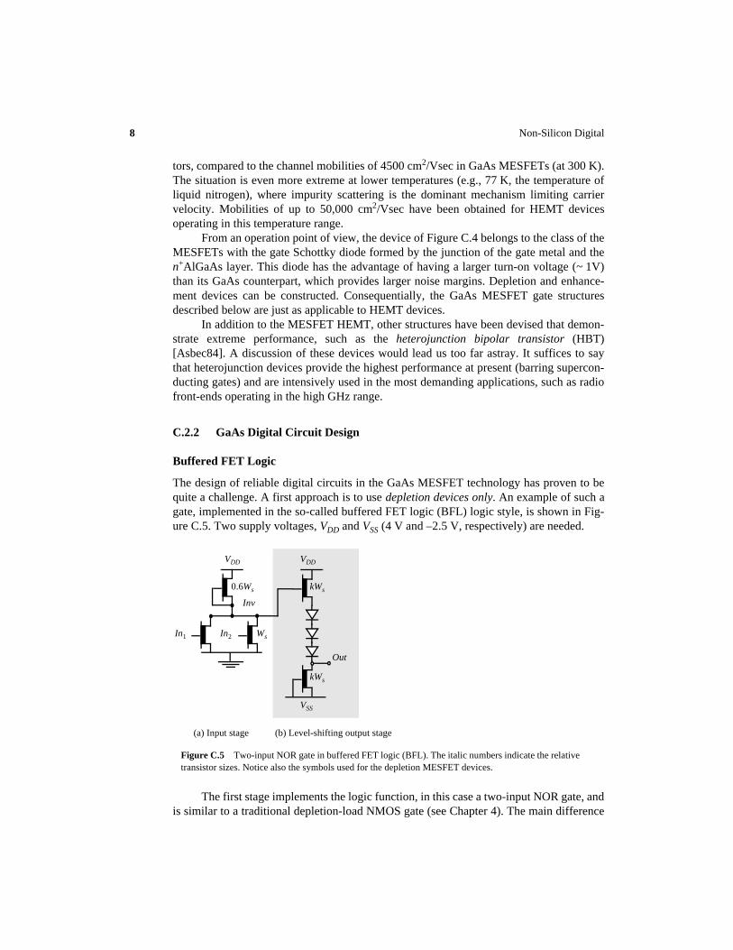
C.2.2 GaAs Digital Circuit Design
Buffered FET Logic
The design of reliable digital circuits in the GaAs MESFET technology has proven to bequite a challenge. A first approach is to use depletion devices only. An example of such agate, implemented in the so-called buffered FET logic (BFL) logic style, is shown in Fig-ure C.5. Two supply voltages, VDD and VSS (4 V and –2.5 V, respectively) are needed.
The first stage implements the logic function, in this case a two-input NOR gate, andis similar to a traditional depletion-load NMOS gate (see Chapter 4). The main difference
Figure C.5 Two-input NOR gate in buffered FET logic (BFL). The italic numbers indicate the relativetransistor sizes. Notice also the symbols used for the depletion MESFET devices.
Out
In1 In2
VDD VDD
VSS
Ws
0.6Ws kWs
kWs
(b) Level-shifting output stage(a) Input stage
Inv

From the 1st Edition 9
is that the pull-down devices are depletion transistors as well, requiring negative input lev-els to turn them off. The low input level has to be lower than VP. On the other hand, VOHcannot be higher than VD(on), which is the turn-on voltage of the Schottky diode. The out-put of the depletion-load inverter is located between GND and VDD. A source-followeroutput stage with level-shifting diodes is inserted to adjust these levels so that all statedrequirements are met. This output stage has the additional advantage of making the perfor-mance of the gate relatively insensitive to fan-out loading or capacitive loads.
This structure has proven to be relatively insensitive to processing and power-sup-ply variations, which is useful when the processing is not well controlled.
Example C.2 Parameter Variations in BFL
The impact of variations in the pinch-off voltage of the MESFET devices on the dc parame-ters of a nine-input BFL NOR gate was examined in [Milutinovic90]. Changing the thresholdfrom –1.25 V to –2.0 V causes only a 0.6 V shift in the switching threshold VM, while VOH andVOL change by at most 0.2 V. A further change in the pinch-off voltage to –2.2 V causes thegate to fail.
The structure also suffers from three major disadvantages:
1. It is based on ratioed logic, which means rise and fall times can be very different.
2. The power consumption is high. The dissipation per gate is typically between 5 and10 mW, most of which can be attributed to the output stage. This prevents its use inlarge-scale designs (> 2000 gates).
3. It uses two supply voltages, which is not attractive from a system perspective.
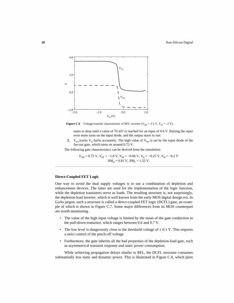
Example C.3 DC Characteristics of the BFL Inverter
A BFL inverter is designed using the depletion devices characterized in Table C.1. Alldevices have a (W/L) ratio of (4 µm/1 µm) with the exception of the load device, which ismade 0.6 times smaller. The supply voltages VDD and VSS are set at 3.5 V and –2 V,respectively.
The current through the inverter stage is approximated by the following expression,assuming that both devices are on and that all Schottky diodes are off:
Solving this equation for various values of Vin yields the voltage-transfer characteristic of theinput stage. Finding this solution is made complex by the presence of the transcendental func-tions. This can be addressed by using recursive equations solvers. For instance, for Vin = 0V, aVout of 0.25 V is found, which is extremely close to the simulated value. The results of a dcanalysis are found in Figure C.6 for a fan-out of one identical gate. The simulation plots theoutput of the inverter as well as the buffer stages. Two issues are worth raising:
1. For input values lower than the threshold of the input transistor, the output of the bufferstage (Vinv) is high and equals 3.5 V. Once the input device is turned on, the output
3.850.6
---------- Vin 0.825+( )2 1 0.0625V0+( ) 3.5Vo( )tanh
2.250.6
---------- 0.825( )2 1 0.0625 3.5 Vo–( )+( ) 3.5 3.5 Vo–( )( )tanh=
10 Non-Silicon Digital
starts to drop until a value of 70 mV is reached for an input of 0.6 V. Raising the inputeven more turns on the input diode, and the output starts to rise.
2. Vout tracks Vin fairly accurately. The high value of Vout is set by the input diode of thefan-out gate, which turns on around 0.75 V.
The following gate characteristics can be derived from the simulation:
VOH = 0.75 V, VOL = −1.8 V, VIH = −0.06 V, VIL = −0.25 V, VM = −0.2 VNMH = 0.81 V, NML = 1.55 V.
Direct-Coupled FET Logic
One way to avoid the dual supply voltages is to use a combination of depletion andenhancement devices. The latter are used for the implementation of the logic function,while the depletion transistors serve as loads. The resulting structure is, not surprisingly,the depletion-load inverter, which is well known from the early MOS digital design era. InGaAs jargon, such a structure is called a direct-coupled FET logic (DCFL) gate, an exam-ple of which is shown in Figure C.7. Some major differences from its MOS counterpartare worth mentioning.
• The value of the high input voltage is limited by the onset of the gate conduction inthe pull-down transistor, which ranges between 0.6 and 0.7 V.
• The low level is dangerously close to the threshold voltage of ± 0.1 V. This requiresa strict control of the pinch-off voltage.
• Furthermore, the gate inherits all the bad properties of the depletion-load gate, suchas asymmetrical transient response and static power consumption.
While achieving propagation delays similar to BFL, the DCFL structure consumessubstantially less static and dynamic power. This is illustrated in Figure C.8, which plots
Figure C.6 Voltage-transfer characteristic of BFL inverter (VDD = 3.5 V, VSS = –2 V).
–2.0 –1.0 0.0 1.0Vin (V)
–2.0
0.0
2.0
4.0
V
Vout
Vinv

From the 1st Edition 11
the propagation delay of DCFL and BFL gates as a function of the power consumption, alldesigned in a 1 micron technology. An order of magnitude difference in power dissipationis observed for similar performance, if one manages to keep the threshold under control.The BFL gate, on the other hand, has superior fan-out driving capabilities.
Source-Coupled FET Logic
The concerns about the limitations of FET threshold control in DCFL have prompted thedevelopment of another logic family with a wide allowable threshold range. The inspira-tion for this family, called source-coupled FET logic (SCFL), can be directly traced to thebipolar ECL structure. It consists of a differential pair and two source-follower outputbuffers with diode level-shifters (Figure C.9). Proper operation of the gate requires onlythat the input transistors of the differential pair be well matched. As with ECL, the powersupply noise is reduced, making it possible to operate with small noise margins. All otherconsiderations raised with respect to ECL gates, such as differential versus single-ended,are valid here as well. While SCFL overcomes the tight threshold control associatedwith DCFL and is intrinsically faster, its power dissipation is higher than DCFL but lessthan BFL.
Figure C.7 Two-input NOR gate in direct-coupled FET logic (DCFL).
Out
In1 In2
VDD
Figure C.8 Comparing the power consumption and gate delay of DCFL and BFL gates (from [Singh86]).
BFL
DCFL
Power dissipation (mW)
Gat
e de
lay
(pse
c)
1.0 2.0 3.0 4.0 5.0 6.040
50
60
70
80
90
100

12 Non-Silicon Digital
Example C.4 MESFET Source-Follower
Consider an inverter in SCFL with VD(on) = 0.7 V, VOH = −1.3 V, VOL = −1.7 V. Using the tran-sistor parameters of Table C.1, determine the value of the ISF such that the voltage dropbetween the gate and source of the source-follower equals 0.5 V in the midpoint of the volt-age transition (assuming that the Weff / Leff of the source-follower devices equals 10).
In the midpoint of the voltage swing, it holds that Vout = −1.5 V. From the input data,we derive the following data for the source-follower: VDS = 0.8 V and VGS = 0.5 V. Pluggingthese numbers into Eq. (C.1) yields a required drain-source current of 0.21 mA. For this cur-rent level, the voltage drop over the source-follower is virtually constant over the completevoltage range of interest. Because the transistor operates in the saturation region, a variationof only 9 mV can be observed between the high and the low output levels.
It is left as an exercise for the reader to determine the value of RD and the sizes of thetransistors in the current switch. You may assume that ISS = ISF.
GaAs Performance: A Comparison
To put the gates presented here in perspective, Table C.2 presents the measured perfor-mance of a number of GaAs logic families (from [Hodges88]). The table presents thedelay for a fan-out of 1 (tp0), the sensitivity to fan-out (∆tp/FO), and capacitance (∆tp/CL)and the power consumption per gate P.
Figure C.9 Two-input NOR gate in differential source-coupled FET logic (SCFL).
RD
Out–In2
–
RD
In1+ In1
–
In2+
VSS
Out+
Output stage
ISS ISFISF
From the 1st Edition 13
Design Space
Digital GaAs excels in the domain of extremely fast, small-scale integration components—fre-quency dividers, counters, (de) multiplexers—where multi-GHz operation has been achieved.For instance, an 8-bit multiplexer implemented in BFL has been demonstrated to run at 3Gbits/sec. These circuits can be of interest in very high speed communication systems.
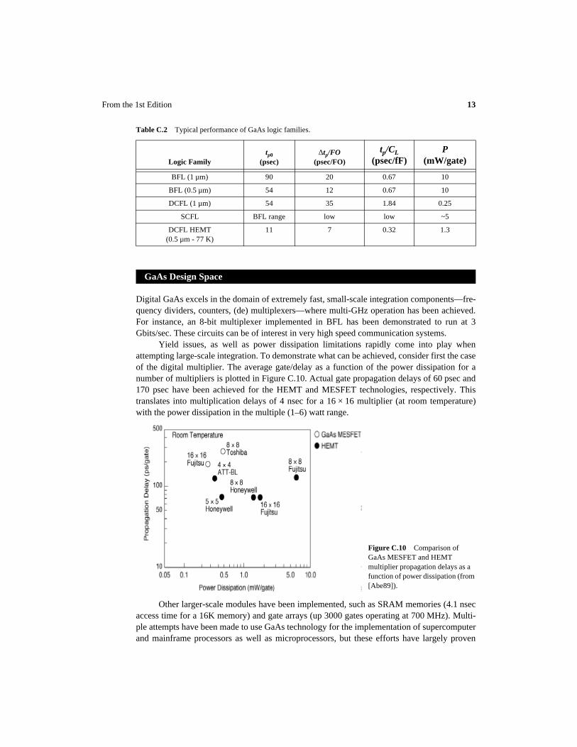
Yield issues, as well as power dissipation limitations rapidly come into play whenattempting large-scale integration. To demonstrate what can be achieved, consider first the caseof the digital multiplier. The average gate/delay as a function of the power dissipation for anumber of multipliers is plotted in Figure C.10. Actual gate propagation delays of 60 psec and170 psec have been achieved for the HEMT and MESFET technologies, respectively. Thistranslates into multiplication delays of 4 nsec for a 16 × 16 multiplier (at room temperature)with the power dissipation in the multiple (1–6) watt range.
Other larger-scale modules have been implemented, such as SRAM memories (4.1 nsecaccess time for a 16K memory) and gate arrays (up 3000 gates operating at 700 MHz). Multi-ple attempts have been made to use GaAs technology for the implementation of supercomputerand mainframe processors as well as microprocessors, but these efforts have largely proven
Table C.2 Typical performance of GaAs logic families.
Logic Familytp0
(psec)∆tp/FO
(psec/FO)
tp/CL (psec/fF)
P (mW/gate)
BFL (1 µm) 90 20 0.67 10
BFL (0.5 µm) 54 12 0.67 10
DCFL (1 µm) 54 35 1.84 0.25
SCFL BFL range low low ~5
DCFL HEMT (0.5 µm - 77 Κ)
11 7 0.32 1.3
GaAs Design Space
Figure C.10 Comparison of GaAs MESFET and HEMT multiplier propagation delays as a function of power dissipation (from [Abe89]).
14 Non-Silicon Digital
unsuccessful. Although working prototypes have been demonstrated, manufacturing and eco-nomic constraints have prevented these components from reaching the market.
C.3 Low-Temperature Digital Circuits *
An alternative approach to higher performance is to operate the devices at lower tempera-tures. The carrier mobility in most devices increases dramatically when the temperature isreduced. Besides the increased mobility, cooling further enhances the performance andreliability of digital integrated circuits, improving the subthreshold slope, the junctionleakage current and capacitance, and the interconnection resistance. Some non-scalableparameters such as the thermal voltage, are also reduced when the temperature is lowered.
While this sounds attractive, cooling comes at substantial cost. High-quality coolersare expensive, bulky, and consume extra power. The most popular cooling media in useare the inert gases, nitrogen and helium, which have boiling temperatures of 77 K and 4.2K, respectively. While liquid nitrogen is inexpensive, and cooling costs are moderate,operating at liquid helium temperatures allows for superconductive operation.
In this section, we briefly discuss the operation of silicon at lower temperatures aswell as the nature and potential of superconducting digital circuitry.
C.3.1 Low-Temperature Silicon Digital Circuits
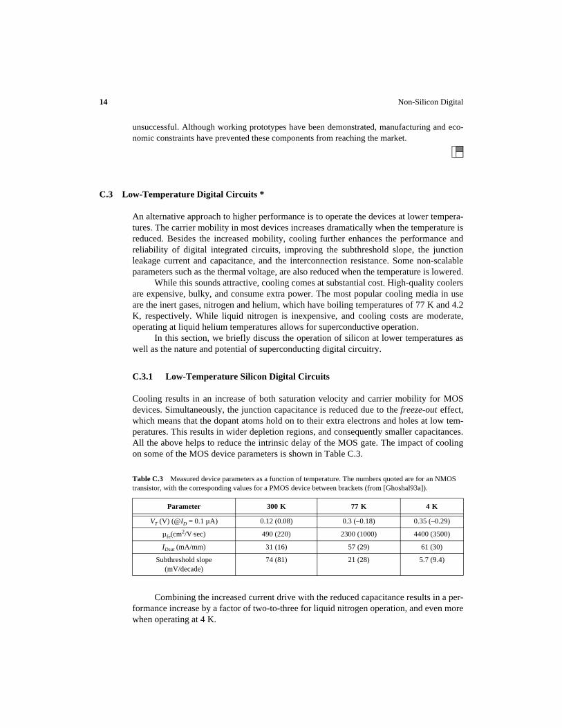
Cooling results in an increase of both saturation velocity and carrier mobility for MOSdevices. Simultaneously, the junction capacitance is reduced due to the freeze-out effect,which means that the dopant atoms hold on to their extra electrons and holes at low tem-peratures. This results in wider depletion regions, and consequently smaller capacitances.All the above helps to reduce the intrinsic delay of the MOS gate. The impact of coolingon some of the MOS device parameters is shown in Table C.3.
Combining the increased current drive with the reduced capacitance results in a per-formance increase by a factor of two-to-three for liquid nitrogen operation, and even morewhen operating at 4 K.
Table C.3 Measured device parameters as a function of temperature. The numbers quoted are for an NMOS transistor, with the corresponding values for a PMOS device between brackets (from [Ghoshal93a]).
Parameter 300 K 77 K 4 K
VT (V) (@ID = 0.1 µA) 0.12 (0.08) 0.3 (–0.18) 0.35 (–0.29)
µfe(cm2/V·sec) 490 (220) 2300 (1000) 4400 (3500)
IDsat (mA/mm) 31 (16) 57 (29) 61 (30)
Subthreshold slope (mV/decade)
74 (81) 21 (28) 5.7 (9.4)
From the 1st Edition 15
At the same time, leakage currents are substantially reduced, because the leakagecurrent of a junction (IS) is a strong function of the temperature . The reducedsub-threshold slope of the device further reduces leakage and makes it possible to operateat lower threshold voltages. At 4 K, a dynamic gate behaves as a static structure, andrefresh is no longer necessary.
Finally, reducing the temperature also decreases the interconnect resistivity, becausethe carriers have less thermal energy, and the scattering rate is subsequentially reduced. Atliquid nitrogen temperatures, the resistance of aluminum wires improves by a factor fiveto six [Bakoglu90].
Besides the cost and difficulty of the providing high-quality cooling environments,operation at a reduced temperature has some disadvantages.
• The mentioned carrier freeze-out increases the resistance of the source and drainregions, since fewer mobile carriers are available. It also causes the threshold volt-age to increase, as Table C.3 shows. Due to the freeze-out, less of the ion-implantedimpurities in the channel are being ionized.
• Threshold voltages in cooled MOS devices tend to drift with time due to hot-elec-tron trapping effects, as carriers injected into the gate are more likely to be trapped.This effect can be remedied by operating at lower voltages.
• The current gain of bipolar devices degrades at lower temperatures due to bandgapnarrowing and reduced emitter-base injection. While this helps to suppress parasiticeffects such as latchup and subthreshold conduction in MOS transistors, it precludesthe use of bipolar gates at temperatures lower than 77 K.
Cooling has been frequently used in the design of high-performance mainframe andsupercomputing systems. For instance, the ETA supercomputer (1987) uses liquid nitro-gen cooling to reduce its cycle time from 14 nsec at room temperature to 7 nsec. Anotheremerging approach is to combine MOS silicon structures with superconducting logic. Thisexploits the extreme performance of the superconducting circuitry with the high density ofMOS. It is worth noting that dynamic circuits exhibit a better behavior at liquid heliumtemperatures, as leakage is eliminated and noise signals are reduced [Ghoshal93b].
C.3.2 Superconducting Logic Circuits
The use of superconductivity in digital circuits dates back to the 1950s. The developmentof the Josephson junction at IBM [Josephson62] spurred the quest for a superconductingcomputer. While this effort faltered in the early 1980s, the 1990s witnessed a renewedinterest in this technology for two reasons: (1) the discovery of high-temperature, super-conducting alloys, and (2) the introduction of niobium junctions, which provide increasedreliability and performance compared to the earlier lead-alloy-based junctions. Before dis-cussing the Josephson junction, which is the prime switching element in superconductinglogic, we first describe superconductivity.
~eqVj kT⁄( )
16 Non-Silicon Digital
Superconductivity
A number of materials have the property to conduct current without resistance whencooled below a critical temperature Tc. Until recently, most of the known superconductingmaterials exhibited this desirable property only when cooled close to absolute zero. In thelate 1980s, a new class of superconducting ceramic materials was discovered with criticaltemperatures around and above 100 K. This discovery is important, because it substan-tially reduces the cooling cost, using liquid nitrogen as a coolant. New composites withever higher critical temperatures are still being discovered, raising hopes for the availabil-ity of room-temperature superconductivity in the near future. One warning with respect tothose materials should be heeded: the onset of superconductivity is not only a function ofthe temperature, but also of the density of the current flowing through the material (J) andthe magnetic field present (Φ).
(C.5)
Raising either the current density or the magnetic field above a critical value causesthe material to revert to the resistive state. For instance, the compound materialyttrium-barium-copper-oxide (or YBCO) has a nominal critical temperature of 95 K,which is substantially above the 77 K of liquid nitrogen. Unfortunately, the maximum cur-rent density allowed at 77 K equals 4 µA/µ2, which is too low to be useful in digital circuitdesign.
The potential impact of superconductivity on circuit design is quite large. It enablesthe transmission of signals over long wires without any resistive loss. This decreases thepropagation delay while lowering the power dissipation. Currents can be stored in induc-tive loops for an almost infinite time, providing for a simple memory structure. In contrastto most digital circuits that can be modeled as RC-networks, the first-order model for asuperconducting component is closer to an LC-network.
The most obvious application of superconductivity in the digital arena is to use tra-ditional devices such as MOS transistors, interconnected by superconducting wires. Whilethis approach helps to address some of the interconnect issues raised in Chapter 8, itsimpact on overall circuit performance is limited, affecting only the delay of the RC-domi-nated wires. A potential application is the distribution of clocks with minimal skew.
More impressive performance benefits are obtained when employing superconduct-ing switching devices as well. Using this approach, switching delays in the range of pico-seconds can be obtained, which is almost an order of magnitude faster than what can beobtained with semiconductor devices. The most popular of these devices is the Josephsonjunction.
The Josephson Junction
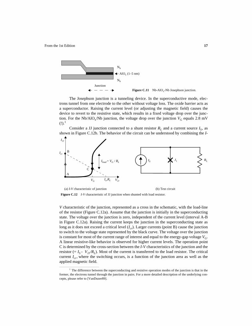
The Josephson junction (abbreviated JJ) was discovered in the early 1960s at the IBMWatson center [Josephson62]. It consists of two layers of superconducting material sepa-rated by a very thin insulator (between 1 and 5 nm), as shown in Figure C.11. The materialof choice in current superconducting design is niobium, which has a critical temperatureof 9 K. The niobium process has the advantage of being substantially more reliable thanthe lead-alloy processes used in the earlier JJ implementations.
Tc f J Φ,( )=
From the 1st Edition 17
The Josephson junction is a tunneling device. In the superconductive mode, elec-trons tunnel from one electrode to the other without voltage loss. The oxide barrier acts asa superconductor. Raising the current level (or adjusting the magnetic field) causes thedevice to revert to the resistive state, which results in a fixed voltage drop over the junc-tion. For the Nb/AlOx/Nb junction, the voltage drop over the junction VG equals 2.8 mV(!).1
Consider a JJ junction connected to a shunt resistor RL and a current source IS, asshown in Figure C.12b. The behavior of the circuit can be understood by combining the I-
V characteristic of the junction, represented as a cross in the schematic, with the load-lineof the resistor (Figure C.12a). Assume that the junction is initially in the superconductingstate. The voltage over the junction is zero, independent of the current level (interval A-Bin Figure C.12a). Raising the current keeps the junction in the superconducting state aslong as it does not exceed a critical level (Icr). Larger currents (point B) cause the junctionto switch to the voltage state represented by the black curve. The voltage over the junctionis constant for most of the current range of interest and equal to the energy-gap voltage VG.A linear resistive-like behavior is observed for higher current levels. The operation pointC is determined by the cross-section between the I-V characteristics of the junction and theresistor (= IS − VJJ /RL). Most of the current is transferred to the load resistor. The criticalcurrent Icr, where the switching occurs, is a function of the junction area as well as theapplied magnetic field.
1 The difference between the superconducting and resistive operation modes of the junction is that in theformer, the electrons tunnel through the junction in pairs. For a more detailed description of the underlying con-cepts, please refer to [VanDuzer89].
Nb
Nb
AlOx (1–5 nm)
Figure C.11 Nb-AlOx-Nb Josephson junction.Junction
Figure C.12 I-V characteristic of JJ junction when shunted with load resistor.
VG VJJ
IJJ
Icr
IS RLJ1Iload = VG / RL
IcrRL
(a) I-V characteristic of junction (b) Test circuit
A
B
C
18 Non-Silicon Digital
As is apparent in Figure C.12a, the Josephson junction displays a hysteresis-likebehavior. The junction remains in the voltage stage, even when the current level isdropped below Icr. For the junction to revert to the superconductive state, it is necessary toreduce the current level to zero, as illustrated by the arrow on the curve.
From the above discussion, it becomes clear that the junction can be modeled as atwo-terminal device with two operation modes: the superconducting, zero-voltage and theresistive, fixed-voltage state. In a typical operation, the junction is biased with a currentIbias, slightly smaller than the critical current Icr. If a switching action is required, the cur-rent is slightly raised, causing the junction to revert to the resistive state. Anotherapproach is to apply a magnetic field so that the critical current Icr is lowered below Ibias,which has a similar effect (Eq. (C.5)). Lowering the biasing current to zero resets thedevice to the superconducting state, after which the next operation cycle can commence.
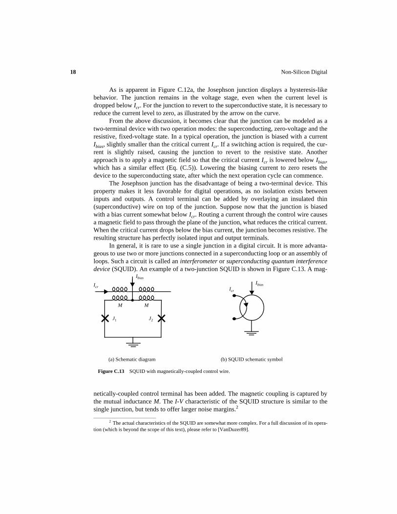
The Josephson junction has the disadvantage of being a two-terminal device. Thisproperty makes it less favorable for digital operations, as no isolation exists betweeninputs and outputs. A control terminal can be added by overlaying an insulated thin(superconductive) wire on top of the junction. Suppose now that the junction is biasedwith a bias current somewhat below Icr. Routing a current through the control wire causesa magnetic field to pass through the plane of the junction, what reduces the critical current.When the critical current drops below the bias current, the junction becomes resistive. Theresulting structure has perfectly isolated input and output terminals.
In general, it is rare to use a single junction in a digital circuit. It is more advanta-geous to use two or more junctions connected in a superconducting loop or an assembly ofloops. Such a circuit is called an interferometer or superconducting quantum interferencedevice (SQUID). An example of a two-junction SQUID is shown in Figure C.13. A mag-
netically-coupled control terminal has been added. The magnetic coupling is captured bythe mutual inductance M. The I-V characteristic of the SQUID structure is similar to thesingle junction, but tends to offer larger noise margins.2
2 The actual characteristics of the SQUID are somewhat more complex. For a full discussion of its opera-tion (which is beyond the scope of this text), please refer to [VanDuzer89].
Figure C.13 SQUID with magnetically-coupled control wire.
Ibias
Icr
MM
J1 J2
IbiasIcr
(a) Schematic diagram (b) SQUID schematic symbol

From the 1st Edition 19
The main attraction of the Josephson junction is its extremely fast switching time.Gate delays in the range of picoseconds have been recorded, which is substantially belowwhat can be achieved in semiconductor technologies, and opens the door for multi-GHzdigital circuits. The switching speed is mostly limited by parasitic circuit effects, not byintrinsic constraints. One word of caution: while switching from the superconductive tothe resistive state proceeds with incredible speed, the reverse operation (the resetting ofthe junction) is comparatively slow and can take up to 20 psec. The reset phase can becompared to the precharging operation in dynamic MOS circuits. As in the dynamicapproach, the impact of the “dead time” on the overall performance can be minimized byadopting the correct system architecture. For instance, it is typical for JJ circuits to operatein a pipelined mode with multiple clocks, where one stage is evaluating while the othersare being reset.
Superconducting Digital Circuits
On the basis of the type of control mechanism employed, we can divide Josephson digitalcircuits into two classes. In the first class, switching between the two states is accom-plished by current overdrive or current injection, while the second class uses magneticcoupling [Hasuo89]. The concepts behind both approaches are illustrated in Figure C.14,where simplified implementations of a two-input OR gate are shown.
Consider first the current-injection approach (Figure C.14a). The SQUIDs are pow-ered by a pulsed current source, which delivers a current Ibias, smaller than Icr. If none ofthe inputs is high, the junctions in the SQUID stay in the superconducting mode, andVout = 0 V. If either input A or B is high, an extra current flows into the loop through theresistors RL. The combination of the bias and the injected currents exceeds the critical cur-rent and causes the junctions in the loop to become resistive. The output of the gate moves
Ibias Ibias Ibias
RL
IA
IB
Ibias IbiasIbias
RLRL
RL
RL
VA
VB
Ibias
reset phase
Figure C.14 Josephson junction logic families.
(a) Current-injection gate with fan-out
(b) Magnetically coupled gate with fan-out
(c) Bias current waveform
Vout
Vout
Fan-out gates
Fan-out gates
20 Non-Silicon Digital
from 0 V in the superconducting state to the gap voltage of 2.8 mV. The bias current isdiverted from the loop into the connecting fan-out gates, assuming that the on-resistanceof the junctions is higher than RL. Since the output current flows into the SQUID loop ofthe connecting gates (which is equivalent to stating that the input-impedance of the gate issmall), fan-out gates must be connected in parallel.
The magnetically coupled approach (Figure C.14b) relies on a similar idea. If bothinputs are low, the SQUID operates in the superconducting mode (Vout = 0 V). Applyingan input current to one (or both) of the inputs generates a magnetic field that reduces thecritical current below the applied bias current. The SQUID switches to the resistive state,and the output switches to high (Vout = 2.8 mV). As the input of the gate is physically iso-lated from the output due to the magnetic coupling, the output signal can be serially con-nected to multiple cascaded gates.
To initiate the next logic operation, the bias current is lowered to zero (FigureC.14c), and the junctions are reset to the superconducting state.
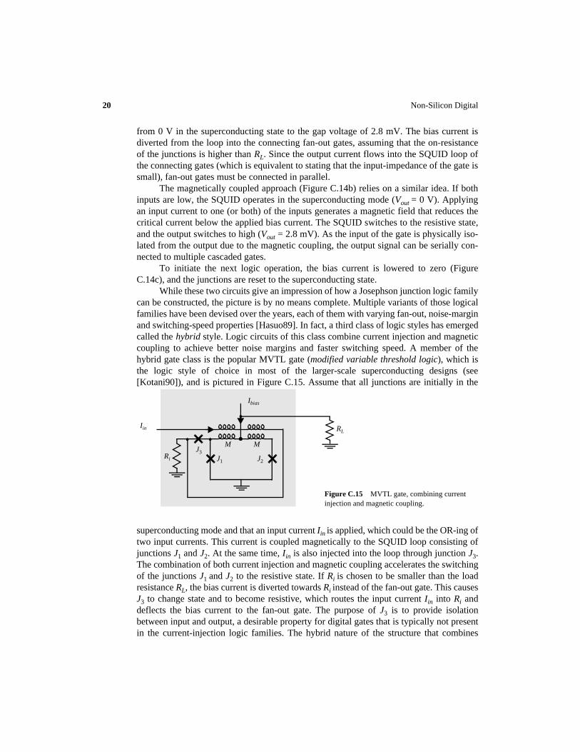
While these two circuits give an impression of how a Josephson junction logic familycan be constructed, the picture is by no means complete. Multiple variants of those logicalfamilies have been devised over the years, each of them with varying fan-out, noise-marginand switching-speed properties [Hasuo89]. In fact, a third class of logic styles has emergedcalled the hybrid style. Logic circuits of this class combine current injection and magneticcoupling to achieve better noise margins and faster switching speed. A member of thehybrid gate class is the popular MVTL gate (modified variable threshold logic), which isthe logic style of choice in most of the larger-scale superconducting designs (see[Kotani90]), and is pictured in Figure C.15. Assume that all junctions are initially in the
superconducting mode and that an input current Iin is applied, which could be the OR-ing oftwo input currents. This current is coupled magnetically to the SQUID loop consisting ofjunctions J1 and J2. At the same time, Iin is also injected into the loop through junction J3.The combination of both current injection and magnetic coupling accelerates the switchingof the junctions J1 and J2 to the resistive state. If Ri is chosen to be smaller than the loadresistance RL, the bias current is diverted towards Ri instead of the fan-out gate. This causesJ3 to change state and to become resistive, which routes the input current Iin into Ri anddeflects the bias current to the fan-out gate. The purpose of J3 is to provide isolationbetween input and output, a desirable property for digital gates that is typically not presentin the current-injection logic families. The hybrid nature of the structure that combines
Figure C.15 MVTL gate, combining current injection and magnetic coupling.
Ibias
Iin
MM
J1 J2
J3Ri
RL
From the 1st Edition 21
injection and coupling results in extra-fast operation speeds. In fact, propagation delays of1.5 psec (!) have been measured for a two-input MVTL OR-gate with a single fan-out.
Example C.5 An MVTL Gate
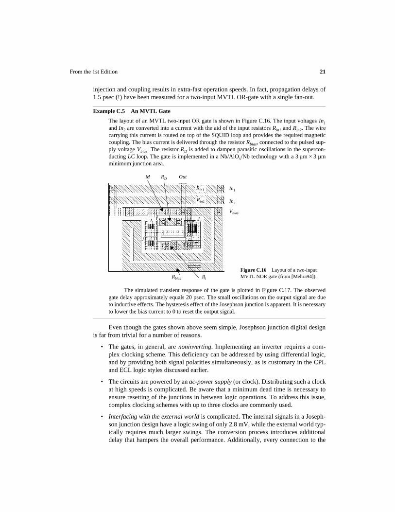
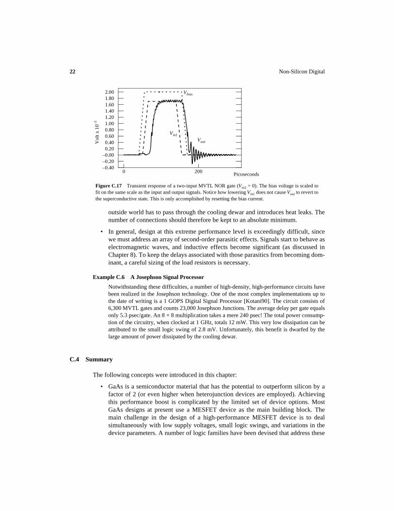
The layout of an MVTL two-input OR gate is shown in Figure C.16. The input voltages In1and In2 are converted into a current with the aid of the input resistors Rin1 and Rin2. The wirecarrying this current is routed on top of the SQUID loop and provides the required magneticcoupling. The bias current is delivered through the resistor Rbias, connected to the pulsed sup-ply voltage Vbias. The resistor RD is added to dampen parasitic oscillations in the supercon-ducting LC loop. The gate is implemented in a Nb/AlOx/Nb technology with a 3 µm × 3 µmminimum junction area.
The simulated transient response of the gate is plotted in Figure C.17. The observedgate delay approximately equals 20 psec. The small oscillations on the output signal are dueto inductive effects. The hysteresis effect of the Josephson junction is apparent. It is necessaryto lower the bias current to 0 to reset the output signal.
Even though the gates shown above seem simple, Josephson junction digital designis far from trivial for a number of reasons.
• The gates, in general, are noninverting. Implementing an inverter requires a com-plex clocking scheme. This deficiency can be addressed by using differential logic,and by providing both signal polarities simultaneously, as is customary in the CPLand ECL logic styles discussed earlier.
• The circuits are powered by an ac-power supply (or clock). Distributing such a clockat high speeds is complicated. Be aware that a minimum dead time is necessary toensure resetting of the junctions in between logic operations. To address this issue,complex clocking schemes with up to three clocks are commonly used.
• Interfacing with the external world is complicated. The internal signals in a Joseph-son junction design have a logic swing of only 2.8 mV, while the external world typ-ically requires much larger swings. The conversion process introduces additionaldelay that hampers the overall performance. Additionally, every connection to the
J3
In1
In2
J2
RD Out
Rbias
Vbias
M
Ri
Rin1
Rin2
Figure C.16 Layout of a two-input MVTL NOR gate (from [Mehra94]).
J1
22 Non-Silicon Digital
outside world has to pass through the cooling dewar and introduces heat leaks. Thenumber of connections should therefore be kept to an absolute minimum.
• In general, design at this extreme performance level is exceedingly difficult, sincewe must address an array of second-order parasitic effects. Signals start to behave aselectromagnetic waves, and inductive effects become significant (as discussed inChapter 8). To keep the delays associated with those parasitics from becoming dom-inant, a careful sizing of the load resistors is necessary.
Example C.6 A Josephson Signal Processor
Notwithstanding these difficulties, a number of high-density, high-performance circuits havebeen realized in the Josephson technology. One of the most complex implementations up tothe date of writing is a 1 GOPS Digital Signal Processor [Kotani90]. The circuit consists of6,300 MVTL gates and counts 23,000 Josephson Junctions. The average delay per gate equalsonly 5.3 psec/gate. An 8 × 8 multiplication takes a mere 240 psec! The total power consump-tion of the circuitry, when clocked at 1 GHz, totals 12 mW. This very low dissipation can beattributed to the small logic swing of 2.8 mV. Unfortunately, this benefit is dwarfed by thelarge amount of power dissipated by the cooling dewar.
C.4 Summary
The following concepts were introduced in this chapter:
• GaAs is a semiconductor material that has the potential to outperform silicon by afactor of 2 (or even higher when heterojunction devices are employed). Achievingthis performance boost is complicated by the limited set of device options. MostGaAs designs at present use a MESFET device as the main building block. Themain challenge in the design of a high-performance MESFET device is to dealsimultaneously with low supply voltages, small logic swings, and variations in thedevice parameters. A number of logic families have been devised that address these
Vol
t x 1
0–3
Picoseconds–0.40–0.20–0.00
0.200.400.600.801.001.201.401.601.802.00
0 200
Vbias
Vout
Vin1
Figure C.17 Transient response of a two-input MVTL NOR gate (Vin2 = 0). The bias voltage is scaled tofit on the same scale as the input and output signals. Notice how lowering Vin1 does not cause Vout to revert tothe superconductive state. This is only accomplished by resetting the bias current.
From the 1st Edition 23
issues. The most popular ones are BFL, DFL, and SCFL. GaAs designs are attrac-tive for the implementation of small building blocks with very high performance,such as those needed in networking and communication systems.
• Heterojunction devices are gaining rapid recognition as one of the promising tech-niques for future very high performance design. They exploit the high carrier veloc-ity obtained at low doping levels in GaAs and in other compound semiconductorssuch as silicon-germanium (SiGe).
• Reducing the ambient operating temperature of a digital circuit results in a signifi-cant performance improvement. Cooling a silicon MOS design to the liquid nitrogenrange boosts the performance by a factor 2 to 3.
• The fastest digital devices at present use the superconducting technology andachieve switching speeds in the picosecond range. The fundamental building blockfor most of these designs is the Josephson junction, a current/flux-controlled devicewith a hysteresis-like behavior. The high performance does not come for free. Pro-viding the necessary cooling medium requires an expensive, bulky dewar. Design atthese high speeds is also anything but easy. The main application domain of thesedevices has therefore been in areas where this extreme performance is essential,such as instrumentation.
• A number of exciting developments, such as the emergence of the high-temperaturesuperconductors, hybrid silicon-superconductor, and other new devices, such as fluxquantum transistors, might change this picture in the coming decades.
This addendum concludes with a philosophical consideration. The chapter demon-strates that achieving extreme switching speeds comes at a substantial cost in designeffort. Traditional design methodologies and design automation techniques become use-less. Interconnections become a significant part of the circuit schematic at these high fre-quencies and introduce noise and delay. The design of a reliable high-performance circuittypically turns into a lengthy analysis and optimization process. It is furthermore not obvi-ous that scaling technologies into the deep submicron regions will result in sustained per-formance improvements. Power considerations, for instance, might provide an upper limiton the switching frequencies that are attainable.
Before opting for one of the higher performing, but less designer-friendly and expen-sive design technologies, we should consider if the performance gain cannot be obtainedby other means, for instance by using concurrent processing. Too often the clock speed isused as the dominant performance metric. Frequently, the same system performance canbe obtained by running multiple slower elements in parallel. This might come at someexpense in area but with greatly reduced design effort. This tendency is becoming preva-lent in the high-performance computer arena, where supermainframe computers with theirextremely high switching speeds are gradually losing out against parallel implementations.
24 Non-Silicon Digital
C.5 To Probe Further
A number of specialized textbooks have recently been published on GaAs digital design, anumber of which are listed below. Excellent overviews of the state-of-the-art techniquescan be found in [Long90]. Once again, the IEEE Journal of Solid-State Circuits and theISSCC conference proceedings are the common source to consult regarding the latestdevelopments in each of these technologies.
REFERENCES
[Abe89] M. Abe et al., “Ultrahigh-Speed HEMT LSI Circuits”, in Submicron Integrated Circuits,ed. R. Watts, Wiley, pp. 176-203, 1989.
[Alvarez89] A. Alvarez, BiCMOS Technology and Applications, Kluwer Academic Publishers, Bos-ton, 1989.
[Asbec84] P. Asbec et al., “Application of Heterojunction Bipolar Transitsors to High-Speed, SmallScale Digital Integrated Circuits,” IEEE GaAs IC Symposium, pp. 133–136, 1984.
[Bakoglu90] H. Bakoglu, Circuits, Interconnections and Packaging for VLSI, Addison-Wesley,1990.
[Buchanan90] J. Buchanan, CMOS/TTL Digital Systems Design, McGraw-Hill, 1990.[Chen92] C. Chen, “2.5 V Bipolar/CMOS Circuits for 0.25 µm BICMOS Technology,” IEEE Jour-
nal of Solid-State Circuits, vol. 27, no. 4, April 1992.[Chuang92] C.T. Chuang, “Advanced Bipolar Circuits,” IEEE Circuits and Systems Magazine, pp.
32–36, November 1992.[Curtice80] W. Curtice, “A MESFET Model for Use in the Design of GaAs Integrated Circuits,”
IEEE Trans. Microwave Theory and Tech., vol. MTT-28, pp. 448–456, 1980.[Dingle78] R. Dingle et al., “Electron Mobilities in Modulation-Doped Semiconductor Hetero-junc-
tion Superlattices,” Appl. Phys. Letters, vol. 33, no. 7, pp. 665–667, October 1987.[Elmasry94] M. Elmasry, ed., BiCMOS Integrated Circuit Design, IEEE Press, 1994. [Embabi93] S. Embabi, A. Bellaouar, and M. Elmasry, Digital BiCMOS Integrated Circuit Design,
Kluwer Academic Publishers, Boston, 1993.[Ghoshal93a] U. Ghoshal, L. Huynh, T., Van Duzer, and S. Kam, “Low-Voltage, Nonhysteretic
Operation of CMOS Transistors at 4K,” IEEE Electron Device Letters, 1993.[Ghoshal93b] U. Ghoshal, D. Hebert, and T. Van Duzer, “Josephson-CMOS Memories,” 1993
ISSCC Conference, vol. 36, pp. 54–55, 1993.[Greub91] H. Greub et al., “High Performance Standard Cell Library and Modeling Technique for
Differential Advanced Bipolar Current Tree Logic,” IEEE Journal of Solid-State Circuits, vol.26, no. 5, pp 749–762, May 1991.
[Haken89] R. Haken et al., “BiCMOS Process Technology,” in [Alvarez89], pp. 63–124, 1989.[Hasuo89] S. Hasuo and T. Imamura, “Digital Logic Circuits,” Proc. of the IEEE, vol. 77, no. 8, pp.
1177–1193.[Hodges88] D. Hodges and H. Jackson, Analysis and Design of Digital Integrated Circuits,
McGraw-Hill, 1988.[Ichino87] H. Ichino, “A 50-psec 7K-gate Masterslice Using Mixed Cells Consisting of an NTL
Gate and LCML Macrocell,” IEEE Journal of Solid-State Circuits, SC-22, pp. 202–207, 1987.
From the 1st Edition 25
[Josephson62] B. Josephson, “Possible New Effects in Superconductive Tunneling,” Phys. Letters,vol. 1, pp. 251, 1962.
[Jouppi93] N. Jouppi et al., “A 300 MHz 115 W 32b Bipolar ECL Microprocessor,” Dig. TechnicalPapers ISSCC Conf., pp 84–85, 1993.
[Kanopoulos89] N. Kanopoulos, Gallium Arsenide Integrated Circuits: A Systems Perspective,Prentice Hall, 1989.
[Kotani90] S. Kotani et al., “A 1 GOPS 8b Josephson Signal Processor,” Dig. Tech. Papers ISSCCConf., pp. 148–149, February 1990.
[Likharev91] K. Likharev and V. Semenov, “RSFQ Logic/Memory Family: A New Josephson-Junc-tion Technology for Sub-Terahertz-Clock-Frequency Digital Systems,” IEEE Trans. AppliedSupercond., vol. 1, pp. 3–28, March 1991.
[Long90] S. Long and S. Butner, Gallium Arsenide Digital Integrated Circuit Design, McGraw-Hill, 1990.
[Masaki92] A. Masaki, “Deep-Submicron CMOS Warms Up to High-Speed Logic,” IEEE Circuitsand Devices Magazine, pp. 18–24, November 1992.
[Mehra94] R. Mehra, “Digital Filter Design with High Performance Superconducting Technology,”Masters thesis, University of California, Berkeley, 1994.
[Milutinovic90] V. Milutinovic, ed., Microprocessor Design for GaAs Technology, Prentice Hall,1990.
[Raje91] P. Raje et al., “MBiCMOS: A Device and Curcuit Technique Scalable to the Sub-micron,Sub-2V Regime,” Digest of Technical Papers ISSCC Conf., vol. 34, pp. 150–151, February1991.
[Rocchi90] M. Rocchi, High Speed Digital IC Technologies, Artech House, 1990.[Rosseel88] G. Rosseel et al., “Delay Analysis for BiCMOS Drivers,” BCTM, pp. 220–222, 1988.[Rosseel89] G. Rosseel et al., “A single-ended BiCMOS Sense Circuit for Digital Circuits,” Pro-
ceedings ISSCC Conference, pp. 114–115, February 1989.[Singh86] H. Singh et al., “A Comparative Study of GaAs Logic Families Using Universal Shift
Resistors and Self-Aligned Gate Technology,” IEEE GaAs IC Symposium, pp. 11–15, 1986.[Sze69] S. Sze, Physics of Semiconductor Devices, Wiley Interscience, 1969.[Tektronix93] GST-1 Standard Cell IC User Documentation, Tektronix, Portland, 1993.[Toh89] K. Toh et al., “A 23 psec/2.1 mW ECL Gate with an ac-coupled Active Pull-down Emitter-
follower Stage,” IEEE Journal of Solid State Circuits, SC-24, no. 5, pp 1301–1305, 1989.[Van Duzer89] T. Van Duzer, “Superconductor Digital IC’s,” in VLSI Handbook, Ed. J. De Gia-
como, McGraw-Hill, pp. 16.1–16.21, 1989.
C.6 Exercises and Design Problems
For all problems, use the device parameters provided in Chapter 2 (as well as the book cover), unlessotherwise mentioned.
1. [E, None] List the main benefits of using GaAs for digital design. What are the main draw-backs of GaAs circuits?
2. [E, HSPICE] Draw the VTC of the GaAs inverter circuit of Figure C.18. Sweep the input sig-nal between 0 and 0.7 V. Assume (a) a depletion and (b) an enhancement device. Comparethe manual results with the output of HSPICE. Use the following models for the MESFETtransistors.
26 Non-Silicon Digital
.model enh njf+ vto=0.23 beta=250u lambda=0.2 alpha=6.5 ucrit=0 gamds=0 ldel=-0.4u wdel=-0.15u+ rsh=210 n=1.16 is=0.5m level=3 sat=0 acm=1 capop=1 gcap = 1.2 m crat = 0.666
.model dp njf+ vto=-0.825 beta=190u lambda=0.065 alpha=3.5 ucrit=0 gamds=0 ldel=-0.4u wdel=-0.15u+ rsh=210 n=1.18 is=10m level=3 sat=0 acm=1 capop=1 gcap = 1.2 m crat = 0.666
3. [M, HSPICE] Determine the propagation delay of the buffered FET NOR of Example C.3 asa function of the load capacitance (using HSPICE). Use the models given in Problem 2. Forthe Schottky barrier diode, use a MESFET with the drain shorted to the source. Discuss theobtained results.
4. [C, HSPICE]a. Sketch the schematic of a two-input buffered-FET NAND gate. Include the level-shifting
output stage(s). Explain the obtained results. b. Simulate the VTC of the obtained gate (for both inputs). c. What are the power consumption and propagation delay of the circuit of part (b).
5. [E, None] Using the parameters of Table C.3, determine the speed-up obtained when coolinga CMOS inverter from 300 K to 4 K.
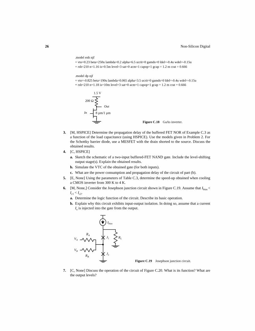
6. [M, None,] Consider the Josephson junction circuit shown in Figure C.19. Assume that Ibias <Ic1 < Ic2.a. Determine the logic function of the circuit. Describe its basic operation.b. Explain why this circuit exhibits input-output isolation. In doing so, assume that a current
Ix is injected into the gate from the output.
7. [C, None] Discuss the operation of the circuit of Figure C.20. What is its function? What arethe output levels?
Out
In
1.5 V
200 Ω
Figure C.18 GaAs inverter.
8 µm/1 µm
RL
J2
RA
RB
VA
VB
J1
Ibias
Figure C.19 Josephson junction circuit.
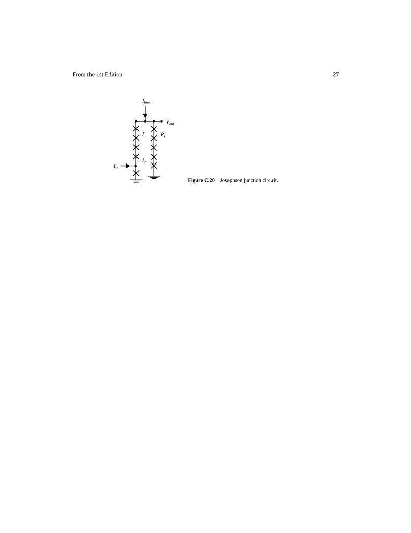
From the 1st Edition 27
RL
J2Iin
J1
Ibias
Figure C.20 Josephson junction circuit.
Vout

![Silicon Nanowire FinFETs - InTechcdn.intechopen.com/pdfs/40046/InTech-Silicon_nanowire_finfets.pdf · [6]. Among all the promising post-CMOS non-conventional structures, the silicon](https://img.pdfslide.us/doc/110x75/5ab1244f7f8b9ac66c8c2378/silicon-nanowire-finfets-6-among-all-the-promising-post-cmos-non-conventional.jpg)