Embed Size (px)
Citation preview
Application Note Please read the Important Notice and Warnings at the end of this document Rev 1.3
www.infineon.com 2018-04-11
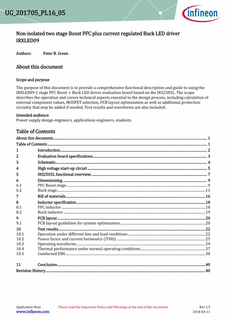
UG_201705_PL16_05
Non-isolated two stage Boost PFC plus current regulated Buck LED driver
IRXLED09
Authors: Peter B. Green
About this document
Scope and purpose
The purpose of this document is to provide a comprehensive functional description and guide to using the IRXLED09 2 stage PFC Boost + Buck LED driver evaluation board based on the IRS2505L. The scope describes the operation and covers technical aspects essential to the design process, including calculation of external component values, MOSFET selection, PCB layout optimization as well as additional protection circuitry that may be added if needed. Test results and waveforms are also included.
Intended audience Power supply design engineers, applications engineers, students.
Table of Contents About this document ......................................................................................................................................................................... 1
Table of Contents ............................................................................................................................................................................... 1
1 Introduction ................................................................................................................................................................. 2
2 Evaluation board specifications ............................................................................................................................. 3
3 Schematic ...................................................................................................................................................................... 4
4 High voltage start-up circuit ................................................................................................................................... 5
5 IRS2505L functional overview ............................................................................................................................... 7
6 Dimensioning .............................................................................................................................................................. 9 6.1 PFC Boost stage .................................................................................................................................................................. 9 6.2 Buck stage ........................................................................................................................................................................... 11
7 Bill of materials ......................................................................................................................................................... 16
8 Inductor specification ............................................................................................................................................. 18 8.1 PFC inductor ...................................................................................................................................................................... 18 8.2 Buck inductor .................................................................................................................................................................... 19
9 PCB layout .................................................................................................................................................................. 20 9.1 PCB layout guidelines for system optimization .................................................................................................. 20
10 Test results ................................................................................................................................................................. 22 10.1 Operation under different line and load conditions ......................................................................................... 22 10.2 Power factor and current harmonics (iTHD) ...................................................................................................... 25 10.3 Operating waveforms .................................................................................................................................................... 29 10.4 Thermal performance under normal operating conditions........................................................................... 37 10.5 Conducted EMI .................................................................................................................................................................. 38
11 Conclusion .................................................................................................................................................................. 40
Revision History ............................................................................................................................................................................... 40

Rev 1.3 Application Note 2 2018-04-11
IRXLED09 Non-isolated two stage Boost PFC plus current regulated Buck LED driver
Introduction
1 Introduction
The IRXLED09 reference design is a low cost two stage non-dimmable LED driver solution. The topology consists of a 90 W wide input range power factor correction Boost converter front end based on the IRS2505L controller IC, followed by a constant current regulated Buck LED driver also based on the IRS2505L. The IRS2505L is a critical conduction mode (CrCM) PFC controller IC primarily intended for front end PFC pre-regulators and typically used in power supply and lighting applications up to 150 W. The IRS2505L based Boost PFC pre-converter is able to meet the requirements of EN61000-3-2, including class C limits for lighting applications. In some cases it is also appropriate to use this controller in other SMPS topologies such as Buck, Buck-Boost and Flyback. The back end Buck stage in this LED driver is configured for constant current (CC) regulation, also operating in critical conduction mode.
The design procedure for a PFC stage based on the IRS2505L differs slightly from the procedure used for industry standard 8 pin CrCM PFC control ICs and will be explained in detail here. In order for the circuit to produce optimum performance care must be taken to select the correct component values and ratings. The PCB must also be designed according to correct practices for SMPS design for which guidelines are provided to avoid ground loops and noise susceptibility. Design of the Buck stage is explained in detail.
In order to save design time simple Excel based design tools are available, which calculate all of the component values based on user inputs as well as providing a simple means for designing the inductors.
Figure 1 IRXLED09 Two stage LED driver board
Figure 2 IRXLED09 Connection diagram

Rev 1.3 Application Note 3 2018-04-11
IRXLED09 Non-isolated two stage Boost PFC plus current regulated Buck LED driver
Evaluation board specifications
2 Evaluation board specifications Input and output at normal operation:
AC Input voltage 90 VAC up to 265 VAC (55 to 65 Hz) Output voltage range at 350+/-25mA output 75 to 200 VDC1 Output voltage range at 700+/-25mA output 40 to 105 VDC2 Maximum HF output current ripple as a percentage of DC average for LED load, 50% Maximum output continuous power 90 W PF >0.95 at maximum load, 90 to 265 VAC input voltage THD <20% at maximum load, 90 to 265 VAC input voltage Efficiency >90% at maximum load at 120 and 230 VAC input voltage. Startup time to reach the secondary nominal output voltage during full load condition and 120 and
230VAC input voltage <300 ms Maximum flicker 20% (including ripple at 2 x line frequency)
Protection features
Primary output over-voltage protection @ VOUT <= 250 VDC Cycle by cycle primary over-current protection
No load operation
Burst mode during no load condition. Max power losses during no load condition <500mW @120 and 230VAC input voltage
Max component temperature During worst case scenario (ambient temperature 60 °C) the max allowed component temperature is:
Resistor < 105 °C Ceramic capacity, film capacity and electrolyte capacity <85 °C Flyback Transformer and chokes <105 °C MOSFET, transistor and diodes <105 °C IC <100 °C
Dimensions of evaluation board
Max width 9.685” (246.0 mm), max length 1.25” (31.8 mm).
WARNING! OUTPUT IS NOT ISOLATED! Risk of electric shock! The board should be tested only by qualified engineers and technicians.
1 IRXLED09 can be operated down to a minimum LED output of 35V at 350mA without flicker. However EN61000-3-2 class C limits
may not be met below the specified minimum voltage. 2 IRXLED09 can be operated down to a minimum LED output of 35V at 700mA without flicker. However EN61000-3-2 class C limits
may not be met below the specified minimum voltage.

Rev 1.3 Application Note 4 2018-04-11
IRXLED09 Non-isolated two stage Boost PFC plus current regulated Buck LED driver
Schematic
3 Schematic
Figure 3 IRXLED09 90 W Two stage Boost PFC Buck LED driver

Rev 1.3 Application Note 5 2018-04-11
IRXLED09 Non-isolated two stage Boost PFC plus current regulated Buck LED driver
High voltage startup circuit (optional)
4 High voltage startup circuit (optional)
To minimize start-up time the IRXLED09 evaluation board includes a high voltage start-up circuit based on the IRS25751L (IC1). This provides a regulated VCC supply current to the PFC Boost stage from the rectified AC line input to rapidly charge the VCC supply capacitor (CVCC2). When the voltage at VCC reaches a level set by the resistor divider formed with RVCC1 and RVCC2, IC1 then turns off and blocks the rectified line voltage while consuming ultra-low leakage current. The HV start-up IC includes an internal 480V NMOS (HVFET) that sources a regulated current (IREG) from the VIN pin to the VOUT pin (Figure 1). The IRS25751L also includes an internal window comparator for turning the current source on and off. The external voltage divider (RVCC1, RVCC2), together with the internal threshold at the VTH pin, determines the upper turn-off threshold for the VOUT pin. An internal voltage divider circuit then sets the fixed lower turn-on threshold for VOUT. The IRS25751L also includes an enable pin (ENN) that can be used to turn off the current source, which is not used in this design. Over-temperature shutdown protection with hysteresis is built-in to shut down and protect the IC in the event of the die temperature ever exceeding 155°C.
5
OTPLogic
1
IREG
41.2V
VIN
ENN
3
VOUT
COM
VTH
4.2V
1.14V
OFF
ON
OFF
OFF
RVCC1
RVCC2
CVCC
DAUX
ON/OFF
(+)
(-)
VCCAuxiliarySupply
High-Voltage DC Bus
20.8V
2
Figure 4 IRS25751L connections and internal block diagram
When AC line voltage is applied to the board, VCC rises as regulated current flows from the IRS25751L VOUT pin into CVCC2. The charge rate is determined by the value of CVCC2 and the IRS25751L output current (IREG). Since IC2 is operating in under voltage lockout it consumes no significant current. CVCC2 is sized to provide enough charge to supply VCC until the auxiliary supply derived from the PFC inductor auxiliary winding is able to over.
When the divided voltage at the VTH input reaches the VOUT+ threshold the current source turns off. The values of RVCC1 and RVCC2 are selected so that this voltage will be above the UVLO+ threshold of the IRS2505L. When the PFC Boost converter starts up the auxiliary supply should take over through the auxiliary supply circuit. If the auxiliary supply does not take over and supply current to VCC then the VOUT pin voltage will start to discharge and will eventually reach the fixed VOUT- lower threshold (4.2V). At this time the current source will turn on again and VOUT will charge back up to the programmed VOUT+ level. The cycle will repeat until the auxiliary supply takes over. In this design additional start-up resistors are also included so that VCC can begin to re-charge as soon as it drops below the UVLO- threshold of the IRS2505L.

Rev 1.3 Application Note 6 2018-04-11
IRXLED09 Non-isolated two stage Boost PFC plus current regulated Buck LED driver
High voltage startup circuit (optional)
VOUT+
VOUT
t
VOUT-
VBUS
VIN
t
IOUT
IOUT
t
ON OFF(auxiliary VCC supply
takes over)
OFF ON
Figure 5 IRS25751L voltage and current waveforms
The upper turn-off VOUT+ threshold is programmed using the following equation:
𝑉𝑂𝑈𝑇+ =𝑅𝑉𝐶𝐶1+𝑅𝑉𝐶𝐶2
𝑅𝑉𝐶𝐶2∙ 𝑉𝑇𝐻+ [V] [1]
1𝑀+91𝑘
91𝑘∙ 1.14 = 13.7𝑉
If RVCC1 is fixed (typically 1MΩ) and the desired VOUT+ threshold is known, then RVCC2 can be calculated using the following equation:
𝑅𝑉𝐶𝐶2 =𝑅𝑉𝐶𝐶1∙𝑉𝑇𝐻+
𝑉𝑂𝑈𝑇+−𝑉𝑇𝐻+ [Ω] [2]
Should the IC junction temperature exceed 155°C then the IRS25751L will shut down so that the internal current source from VIN to VOUT turns off. When the junction temperature decreases again below 100°C (and VOUT is less than VOUT+) then the IC will become enabled again and the internal current source from VIN to VOUT will switch on again. The IC will continue to operate in and out of ON, OFF and over-temperature protection modes until the VCC auxiliary supply properly takes over or the system is shutdown.
In low cost designs the HV start-up can be replaced by two series start-up resistors. The IRXLED09 PCB includes locations for adding these resistors RS1 and RS2.

Rev 1.3 Application Note 7 2018-04-11
IRXLED09 Non-isolated two stage Boost PFC plus current regulated Buck LED driver
IRS2505L functional overview
5 IRS2505L functional overview The IRS2505L critical conduction mode (CrCM) Boost PFC controller IC may also be used as a current regulated Buck controller. All of the functionality for controlling the PFC pre-converter is integrated into the SOT23-5 package. This low pin count solution operates by using multi-functional VBUS and PFC pins so that the cycle by cycle current sense input is combined with the output voltage feedback at the VBUS pin and the zero-crossing (ZX) sensing function is combined with the gate drive at the PFC pin. At the start of each switching cycle the PFC pin gate drive output pulls the PFC pin voltage high and the external MOSFET turns on, where the on-time duration is set by the CMP pin voltage. The internal PFC control loop regulates the CMP pin voltage, which determines the on-time such that if the DC bus voltage increases then the CMP pin voltage and on-time will decrease and vice versa. Decreasing the on time reduces the peak inductor current transferring less energy per switching cycle and causing the DC bus voltage to decrease. If the DC bus voltage decreases below the desired level the CMP pin voltage and on-time will increase to compensate. This negative feedback control loop regulates the DC bus to a constant voltage over AC line voltage or output load variations. The speed of regulation is determined by the internal OTA trans-conductance and compensation capacitor CCMP. At the end of each on time period, the PFC pin gate drive circuit pulls the PFC pin to COM and the external PFC MOSFET turns off. After a short initial switch off delay (tPD), the IRS2505L internal gate drive pull-down turns off and the PFC pin is then weakly pulled up and clamped at approximately one diode forward voltage drop (VPFCOFF), which is well below the gate threshold of the MOSFET (MPFC) ensuring that it is not able to switch on. During the off-time the PFC inductor current discharges through the boost diode into the DC output capacitor and load. When the inductor current falls to zero, the drain voltage falls from the level of the output voltage plus the output diode forward voltage and transitions negatively. During this transition current flows through the MOSFET parasitic gate to drain capacitance CGD overcoming the internal
weak pull up and causing the gate voltage to drop below the threshold VPFCZX-. After remaining below this
threshold for a period of tZXBLANK, the PFC gate drive is turned on again to begin the next switching cycle. To ensure ZX detection a minimum voltage headroom of 60-70V is needed between the peak line voltage at high line and the output voltage. This value depends on the MOSFET CGD and CGS values. To operate with smaller headroom, a 500V minimum rated capacitor of low value in the 10’s of pF range may be added between drain and gate with a 100Ω series resistor to provide some additional –dv/dt coupling to the gate. Since the loop speed is slow with respect to the line frequency the on-time is essentially constant over the entire half cycle of the line input voltage producing a peak inductor current that naturally follows the sinusoidal shape of the line input voltage. The filtered, averaged line input current is in phase with the line input voltage (neglecting a small displacement caused by the input filter X capacitors) to provide high power factor. However some harmonic distortion of the current is still present mostly due to cross-over distortion occurring near the zero-crossings of the line input voltage. To achieve very low harmonics within the limits of international standards and to meet general market requirements, on-time modulation is included in the IRS2505L, which dynamically increases the on-time as the line input voltage nears the zero-crossings. The peak LPFC current and therefore the smoothed line input current increase slightly higher near the zero-crossings of the line input voltage. This reduces the amount of cross-over distortion in the line input current and improves the shape of the current reducing the THD and harmonics to low levels.
The VBUS input includes output over-voltage protection (OVP). Should the average feedback voltage at the VBUS pin exceed the internal over-voltage protection threshold (VBUSOV+) then the PFC gate drive will turn off until the VBUS pin voltage again falls below the over-voltage restart threshold (VBUSOV-) to resume normal operation. As well as sensing the output voltage feedback, the VBUS input also includes a cycle-by-cycle, AC-coupled, over-current protection (OCP) function. An internal over-current protection circuit detects the difference between the peak and average of the composite signal such that if the triangular-shaped voltage peak at the VBUS input exceeds VBUSREG by a delta of VBUSOC+ the gate drive is immediately driven low. Capacitor CVBUS is included to the feedback network to make the current sense signal more triangular rather than a discontinuous ramp. This is so that the peak value will be close to half the average.

Rev 1.3 Application Note 8 2018-04-11
IRXLED09 Non-isolated two stage Boost PFC plus current regulated Buck LED driver
IRS2505L functional overview
The composite voltage and current feedback signal appearing at the VBUS input is shown below:
VCS
t
t
VBUS
DC Offset (from DC bus measurement)
t
PFC
VBUSOC+
Normal Mode OCP Mode
Shaping effect of CVBUS makes
the signal more tr iangular
Figure 6 VBUS input signal
The IRS2505L uses an SOT23-5 package as shown below:
1
3
5
4
IRS
25
05
CMP
PFC
VBUS
VCC
2COM
Pin Name Description
1 CMP High Voltage Start-up Input
2 COM Feedback Input 3 VCC Compensation and averaging capacitor input 4 PFC Zero-Crossing & Over-Voltage Detection input 5 VBUS Current Sensing Input
Figure 7 IRS2505L pin assignments
Rev 1.3 Application Note 9 2018-04-11
IRXLED09 Non-isolated two stage Boost PFC plus current regulated Buck LED driver
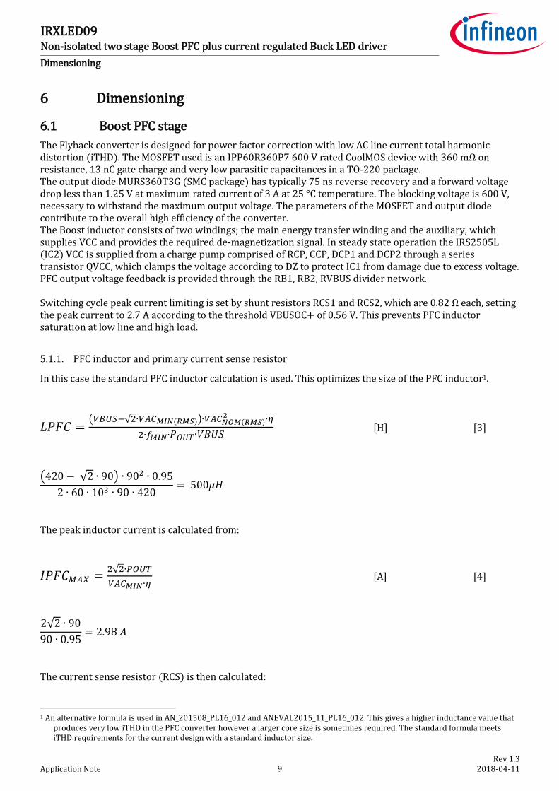
Dimensioning
6 Dimensioning
6.1 Boost PFC stage
The Flyback converter is designed for power factor correction with low AC line current total harmonic distortion (iTHD). The MOSFET used is an IPP60R360P7 600 V rated CoolMOS device with 360 mΩ on resistance, 13 nC gate charge and very low parasitic capacitances in a TO-220 package. The output diode MURS360T3G (SMC package) has typically 75 ns reverse recovery and a forward voltage drop less than 1.25 V at maximum rated current of 3 A at 25 °C temperature. The blocking voltage is 600 V, necessary to withstand the maximum output voltage. The parameters of the MOSFET and output diode contribute to the overall high efficiency of the converter. The Boost inductor consists of two windings; the main energy transfer winding and the auxiliary, which supplies VCC and provides the required de-magnetization signal. In steady state operation the IRS2505L (IC2) VCC is supplied from a charge pump comprised of RCP, CCP, DCP1 and DCP2 through a series transistor QVCC, which clamps the voltage according to DZ to protect IC1 from damage due to excess voltage. PFC output voltage feedback is provided through the RB1, RB2, RVBUS divider network. Switching cycle peak current limiting is set by shunt resistors RCS1 and RCS2, which are 0.82 Ω each, setting the peak current to 2.7 A according to the threshold VBUSOC+ of 0.56 V. This prevents PFC inductor saturation at low line and high load.
5.1.1. PFC inductor and primary current sense resistor
In this case the standard PFC inductor calculation is used. This optimizes the size of the PFC inductor1.
𝐿𝑃𝐹𝐶 =(𝑉𝐵𝑈𝑆−√2∙𝑉𝐴𝐶𝑀𝐼𝑁(𝑅𝑀𝑆))∙𝑉𝐴𝐶𝑁𝑂𝑀(𝑅𝑀𝑆)
2 ∙𝜂
2∙𝑓𝑀𝐼𝑁∙𝑃𝑂𝑈𝑇∙𝑉𝐵𝑈𝑆 [H] [3]
(420 − √2 ∙ 90) ∙ 902 ∙ 0.95
2 ∙ 60 ∙ 103 ∙ 90 ∙ 420= 500𝜇𝐻
The peak inductor current is calculated from:
𝐼𝑃𝐹𝐶𝑀𝐴𝑋 =2√2∙𝑃𝑂𝑈𝑇
𝑉𝐴𝐶𝑀𝐼𝑁∙𝜂 [A] [4]
2√2 ∙ 90
90 ∙ 0.95= 2.98 𝐴
The current sense resistor (RCS) is then calculated:
1 An alternative formula is used in AN_201508_PL16_012 and ANEVAL2015_11_PL16_012. This gives a higher inductance value that
produces very low iTHD in the PFC converter however a larger core size is sometimes required. The standard formula meets iTHD requirements for the current design with a standard inductor size.

Rev 1.3 Application Note 10 2018-04-11
IRXLED09 Non-isolated two stage Boost PFC plus current regulated Buck LED driver
Dimensioning
𝑅𝐶𝑆 =2∙𝑉𝐵𝑈𝑆𝑂𝐶+
𝐼𝑃𝐹𝐶𝑀𝐴𝑋 [Ω] [5]
2 ∙ 0.56
2.98= 0.38 Ω
In this case a parallel combination with a combined resistance of 0.41 Ω has been used.
5.1.2. Voltage feedback and loop compensation
The DC output bus voltage is regulated using a resistor divider to provide feedback to the error amplifier through the VBUS input. The cycle by cycle current sense signal is also superimposed onto this DC voltage however this can be ignored for the purposes of calculating the voltage divider. This is because the voltage feedback and current sense signals are separated within the IRS2505L. The internal reference for the error amplifier VBUSREG is nominally 4.1 V. The resistor divider values are calculated as follows where two equal series resistors RB1 and RB2, are used for the upper branch of the divider:
RB1 and RB2 are selected as 1 MΩ for minimal power dissipation:
𝑃𝑅𝐵1 = 𝑃𝑅𝐵2 ≈ 𝑉𝐵𝑈𝑆
2
2∙(𝑅𝐵1 + 𝑅𝐵2) [W] [6]
4202
2 ∙ (1 ∙ 106 + 1 ∙ 106)≈ 44 𝑚𝑊
Therefore:
𝑅𝑉𝐵𝑈𝑆 = 𝑉𝐵𝑈𝑆𝑅𝐸𝐺∙(𝑅𝐵1+𝑅𝐵2)
𝑉𝐵𝑈𝑆−𝑉𝐵𝑈𝑆𝑅𝐸𝐺 [Ω] [7]
4.1 ∙ (1 ∙ 106 + 1 ∙ 106)
420 − 4.1= 19.7 𝑘Ω
In order for the converter to provide high power factor and low THD the loop response must be slow enough that the on time remains effectively constant (except for on time modulation) throughout each line frequency half cycle. Since the AC line frequency is 50-60 Hz the error amplifier gain has to roll off at a lower frequency. The recommended value for this cut off frequency (or bandwidth) is 20 Hz to give the acceptable loop response without degrading the power factor. The loop speed is determined by the compensation capacitor CCMP whose value is calculated from the trans-conductance of the error amplifier gm (approximately 100µΩ-1) as follows:

Rev 1.3 Application Note 11 2018-04-11
IRXLED09 Non-isolated two stage Boost PFC plus current regulated Buck LED driver
Dimensioning
𝐶𝐶𝑀𝑃 =𝑔𝑚
2𝜋∙𝑓𝑐=
100
2𝜋∙20= 0.796 [µF] [8]
A CCMP value of 0.68 µF is used in the IRXLED09 evaluation board PFC combined with a 33 k series resistor (RCMP) and a 1 nF (CCF) capacitor parallel to both. The series resistor enables VCOMP to jump almost instantly to approximately 1V when VCC first crosses VCCUV+, which reduces the time required for CCMP to charge above VCMPON to enable the gate drive. This reduces the time during which VCC is supplied through CVCC before the auxiliary winding can provide current. The compensation network discussed changes the frequency response of the error amplifier introducing a zero at 7.1 Hz and a pole at 4.8 kHz, while maintaining a gain of approximately 10 dB between these two frequencies. This has the effect of reducing settling time at start up or after a change in line or load.
5.1.3. Output capacitor calculation
The output bulk capacitor (CBUS) can be a single capacitor rated at 450 V for nominal output voltages up to 420 V. This ensures that under start up and transient conditions the output voltage will not exceed the maximum voltage rating. This value can be calculated according to:
𝐶𝐵𝑈𝑆 = 𝑃𝑂𝑈𝑇
2∙𝜋∙𝑓𝐼𝑁(𝑀𝐼𝑁)∙∆𝑅𝐼𝑃𝑃𝐿𝐸∙ 𝑉𝐵𝑈𝑆2 [F] [9]
Where fIN(MIN) is the minimum line input frequency set at 50 Hz and ∆RIPPLE is the fraction of VBUS acceptable as peak to peak ripple amplitude. This should not exceed 16 % to avoid false triggering of the over voltage protection. In this case a value of 0.071 is used corresponding to 30 Vpp.
90
2 ∙ 𝜋 ∙ 50 ∙ 0.071 ∙ 4202= 22 𝜇𝐹
6.2 Buck stage
Regulation of the output current in the Buck stage is performed by feeding back the source current of MBUCK to the VBUS input of IC3. Since the Buck stage also operates in critical conduction mode the current in LBUCK falls to zero at the end of each switching cycle, therefore the average inductor current is equal to half the peak. Much of the high frequency component of the output current passes through the output electrolytic capacitor COUT2, leaving a mostly DC current to drive the LED load. This output current is equal to the average inductor current. Regulation of the peak inductor current therefore provides sufficiently accurate control of the output current.
𝐼𝐵𝑈𝐶𝐾(𝑃𝐾) = 2 ∙ 𝐼𝑂𝑈𝑇 [A] [10]
In practice the effects of output current ripple at the switching frequency cause the peak current to be a little higher than two times the average when driving an LED load.

Rev 1.3 Application Note 12 2018-04-11
IRXLED09 Non-isolated two stage Boost PFC plus current regulated Buck LED driver
Dimensioning
Inductor Current
t
i(t)
Average Inductor Current
Figure 8 Inductor and Output Currents
In the PFC stage the VBUS input to the IRS2505L receives a combined signal containing the output voltage with the current feedback superimposed onto it, where each of these components of the signal varies independently of the other. However the current signal in the Buck regulator is not AC coupled onto a feedback voltage but instead applied directly and always referenced to 0V. This is because the Buck stage operates by current regulation without output voltage feedback. Over-voltage protection is implemented using a separate circuit connected to the CMP pin. This is necessary to allow optimum current regulation accuracy. In the Buck stage the CMP input is not used for regulation therefore a small capacitor CCFB connected, which charges above threshold VCOMPON very rapidly to enable switching operation. The current sense signal can be fed to the IRS2505L input through an RC filter as in the IRXLED09 evaluation board, comprising RC2 and CCS to remove any noise spikes. However since such a filter introduces a delay this creates a difference between the voltage before and after the filter, which is dependent on the signal dv/dt. This introduces a variation in the peak regulation of the inductor current. The propagation delay within the IRS2505L also means that the gate drive does not switch off until the VBUS voltage has ramped slightly above the internal threshold. Again the amount of overshoot increases for higher dv/dt values, which occur at shorter duty cycles. The combination of these factors limits accuracy of output current regulation accuracy for the Buck regulator over output voltage variations for different LED loads.
Current SenseSignal
t
VBUS
Signal average
Signal peak
Comparator threshold
Small overshoot
Larger overshoot
D
Figure 9 Buck stage VBUS input signal
Within the IRS2505L the signal fed to the VBUS input is averaged, which would provide an internal voltage equal to the output voltage DC feedback component (in this case zero) plus the average of the current ramp signal. The cycle by cycle current threshold, which turns off the gate drive to MBUCK, is equal to the average voltage shown by the lower dotted line in the above figure, plus an offset of VBUSOC+ with a typical value of 0.53V.

Rev 1.3 Application Note 13 2018-04-11
IRXLED09 Non-isolated two stage Boost PFC plus current regulated Buck LED driver
Dimensioning
To determine the required shunt resistors (RCS3-7) required at the source of MBUCK the effective threshold must be used which factors in the effect of the internal average. For an ideal waveform with no filter and no propagation delay the following formula would apply:
𝑉𝐵𝑈𝑆(𝑇𝐻) ≈ 2∙𝑉𝐵𝑈𝑆𝑂𝐶+
2−(𝑉𝑂𝑈𝑇
𝑉𝐵𝑈𝑆⁄ )
[V] [11]
However for the reasons explained this gives a lower threshold voltage that is observed in reality. The following correction factors are added to give a more accurate result:
𝑉𝐵𝑈𝑆(𝑇𝐻) ≈ 2∙𝑉𝐵𝑈𝑆𝑂𝐶+
2−(𝑉𝑂𝑈𝑇
𝑉𝐵𝑈𝑆⁄ )
+ 0.1 +1−𝐷
200 [V] [12]
The current sense resistor value for a desired average output current is therefore calculated from the maximum LED load voltage as follows:
𝑅𝐶𝑆(𝐵𝑈𝐶𝐾) = 𝑉𝐵𝑈𝑆(𝑇𝐻)
2∙𝐼𝑂𝑈𝑇 [Ω] [13]
This can also be expressed as:
𝑅𝐶𝑆(𝐵𝑈𝐶𝐾) = 𝑉𝐵𝑈𝑆𝑂𝐶+
[ 2−(𝑉𝑂𝑈𝑇
𝑉𝐵𝑈𝑆⁄ )]∙𝐼𝑂𝑈𝑇
+0.1
2∙𝐼𝑂𝑈𝑇 [Ω] [14]
The IRXLED09 board can be selected for 350mA or 700mA output. For 350mA the required resistor is:
0.53
[ 2 − (120420⁄ )] ∙ 0.7
+0.1
2 ∙ 0.7= 0.44Ω
This is provided by the parallel combination of RCS4 and RCS5. For 700mA, the required resistor is:
0.53
[ 2 − (200420⁄ )] ∙ 0.35
+0.1
2 ∙ 0.35= 1.14Ω
This is given by the parallel combination of RCS4-7, which is selected by connecting a link between the terminals of P3 as shown in figure 2. VCC to the Buck stage is supplied through the same charge pump connected to the auxiliary PFC inductor winding. However blocking diode DVCC allows the high voltage start-up regulator to supply the PFC stage only allowing the PFC section to start up and supply VCC to both stages from its auxiliary winding and charge pump.

Rev 1.3 Application Note 14 2018-04-11
IRXLED09 Non-isolated two stage Boost PFC plus current regulated Buck LED driver
Dimensioning
The inductance required for the Buck inductor can be calculated from the following formula:
𝐿𝐵𝑈𝐶𝐾 ≈ 𝑉𝑂𝑈𝑇
2∙𝑓𝑆𝑊∙𝑖𝑂𝑈𝑇∙
(𝑉𝐵𝑈𝑆−𝑉𝑂𝑈𝑇)
𝑉𝐵𝑈𝑆 [H] [15]
200
2 ∙ 120 ∙ 0.35∙
(420 − 200)
420= 1.25𝑚𝐻
The IRXLED09 evaluation board uses a 1mH inductor with a peak current rating of 1.5A. This is acceptable for the application, which also needs to support an output current of 700mA having a peak current of 1.4A. The switching frequency must be lower for a higher peak current so the calculation for a 700mA, 120V load is as follows:
120
2 ∙ 50 ∙ 0.7∙
(420 − 120)
420= 1.22𝑚𝐻
The switching frequency relationship to the inductor value is only approximate in this calculation because losses and ripple are not factored in. Measurements show that the switching frequency tends to be lower than predicted. 6.21 MOSFET selection The CoolMOS IPP60R360P7 and MURS360T3S are also used for the Buck converter stage. Since blocking voltages exist up to the DC bus voltage of 420V, 600V rated devices provide a comfortable safety margin. The CoolMOSTM P7 series is the latest CoolMOSTM product family and targets customers looking for high performance and at the same time being price sensitive. Though optimizing key parameters (Coss, Eoss, Qg, Ciss, and VGS(th) et al. ); integrating Zener Diode for ESD protection and other measures, this product family fully addresses market concerns in performance, ease-of-use, and price/performance ratio, delivering best-in-class performance with exceptional ease-of-use, while still no compromise in price/performance ratio. The 700V and 800V CoolMOSTM P7 series have been designed for flyback and could also be used in PFC topology; they are not recommended for soft switching topologies where hard commutation could happen due to its body diode ruggedness. However, the 600V CoolMOSTM P7 could be used in both soft and hard switching topologies including PFC, flyback, LLC, and TTF.
Figure 10 Switching MOSFET parasitics

Rev 1.3 Application Note 15 2018-04-11
IRXLED09 Non-isolated two stage Boost PFC plus current regulated Buck LED driver
Dimensioning
6.23 Over voltage protection The output terminal DC voltage is limited to 250V by the over voltage protection circuit. This allows 250V rated output capacitors COUT1 and COUT2 to be used, however the outputs are not isolated therefore a high voltage potential to ground and associated electric shock risk exists from either output terminal. If no LED load is connected to clamp the differential output voltage between P2 terminals 1 and 2, this voltage will rise until conduction occurs through RE, the emitter-base junction of PNP transistor QOV1 and DZ2 in series with DZ3. When this occurs QOV1 turns on supplying current through ROV1 and ROV2 to increase the voltage at the cathode of DZ4 until it reaches a high enough voltage to conduct through the base emitter junction of QOV2 to discharge CCFB at the CMP input of IC3 shutting off the gate drive. When the output voltage drops again QOV2 switches off to enable the gate drive again so that the Buck stage may operate. In this way the Buck stage enters hiccup mode during an open load condition as the voltage at the CMP input rises and falls above VCMPON to limit the output to no more than 250V.

Rev 1.3 Application Note 16 2018-04-11
IRXLED09 Non-isolated two stage Boost PFC plus current regulated Buck LED driver
Bill of materials
7 Bill of materials
Designator Manufacturer Part Number Quantity Value/Rating
BR1 Vishay GBU4J-E3/51 1 600V/4A
BUCK, PFC Keystone 5002 2 0.04" dia white
CBUS1 Rubycon, Wurth
450BXF22M12.5X20, 860241478004
1 22µF/450V/20%
CBUS2, CDC Panasonic ECQ-E6334JF 2 0.33µF/630V/5%
CBUS3 TDK C1210C104KCRACTU 1 0.1µF/500V/1210/10%
CC, CCS, CZX TDK CGA4C2C0G2A221J060AA 3 220pF/100V/0805/5% CC1, CVCC1, CVCC3
Wurth 885012207098
3 0.1µF/50V/0805/10%
CCF, CCFB, COV
TDK, Wurth
C2012X7R2E102K085AA, 885342207008
3 1nF/250V/0805/10%
CCMP TDK, Wurth
C2012X7R1E105K125AB, 885012207078
1 1µF/25V/0805/10%
CCP TDK, Wurth
C3216CH1H333K085AA, 885012208084
1 33nF/50V/1206/10%
CGD Wurth 885342008008 1 22pF/1kV/1206
COM1, COM2, COM3
Keystone 5001 3 0.04" dia black
COMP, VBUSBK, ZX
Keystone 5004 3 0.04" dia yellow
COUT1 Panasonic ECQ-E2105KB 1 1µF/250V/10%
COUT2 Rubycon 250-BXF56M12.5X20 1 56µF/250V/20%
CVB Panasonic EEU-EB1H220S 1 22µF/50V
CVBUS TDK, Wurth
C2012X7R2E472K085AA, 885342207009
1 4.7nF/250V/0805/10%
CVCC2 Wurth 860160472006 1 39µF/25V
CX1, CX2 Epcos, Wurth
B32922C3474M, 890324025039
2 0.47µF/305VAC/X2
CY1, CY2 Vishay VY2222M31Y5VS63V7 2 2.2nF/300VAC/Y DBP Diodes Inc RS3JB-13-F 1 600V/3A/SMB
DBUCK, DPFC
ON Semi MURS360T3G 2 600V/3A Fast Recovery Diode
DCP1, DCP2, DVCC
Diodes Inc LL4148-13 3 75V/0.15A/MINIMELF
DG Vishay BAS85-GS08 1 Schottky/30V/200mA/SOD80
DZ1 Micro Commercial Co
BZV55C18-TP 1 18V/0.5W/MINIMELF
DZ2 On Semi MMSZ5272BT3G 1 110V/0.5W/SOD123
DZ3 On Semi UDZLVTE-17100 1 100V/0.2W/SOD323
DZ4 Micro Commercial Co
BZV55C5V6-TP 1 5.6V/0.5W/MINIMELF
F1 Bel Power RST 3.15 1 250V/3.15A
IC1 Infineon IRS25751L 1 HV Start-up IC
IC2, IC3 Infineon IRS2505L 2 PFC Control IC
L1 Epcos B82721A2122N20 1 6.8mH/1.2A/Horiz

Rev 1.3 Application Note 17 2018-04-11
IRXLED09 Non-isolated two stage Boost PFC plus current regulated Buck LED driver
Bill of materials
L2 Bourns 2124-V-RC 1 1mH/1.3A
LBUCK Precision Inc/ Premo
019-8883-00R/ P2456-02
1 1mH/1.6A
LPFC Precision Inc PFC-13500-01 1 500µH/CrCM PFC 100W
MBUCK, MPFC
Infineon IPP60R360P7 2 600V/9A/TO-220
P1 Wurth 691412120003B 1 3 Position 3.5mm Green
P2 Wurth 691412120002B 1 2 Position 3.5mm Green
P3 Wurth 691412120002B 1 2 Position 3.5mm Green
QOV1 Diodes Inc FMMT560TA 1 500V/0.15A/PNP/SOT-23
QOV2, QVCC Micro Commercial Co
BC846B 2 65V/0.1A/NPN/SOT-23
RB1, RB2, RVCC1
Panasonic ERJ-8GEYJ105V 3 1M/0.25W/1206/5%
RBIAS, RZX Panasonic ERJ-6GEYJ103V 2 10k/0.125W/0805/5%
RC1, RC2 Panasonic ERJ-6GEYJ102V 2 1k/0.125W/0805/5%
RCMP Panasonic ERJ-6GEYJ333V 1 33k/0.125W/0805/5%
RCP Panasonic ERJ-14YJ100U 1 10/0.5W/1210/5%
RCS1, RCS2, RCS3
Panasonic ERJ-8BQJ1R0V 3 1.0/0.5W/1206
RCS4, RCS5 Yageo AC1206FR-072R2L 2 2.2/0.25W/1206/1%
RCS6, RCS7 Yageo AC1206FR-071R6L 2 1.6/0.25W/1206/1%
RE Panasonic ERJ-8GEYJ154V 1 150k/0.25W/1206/5%
RS1, RS21 Panasonic ERJ-8GEYJ154V 0 150k/0.25W/1206/5%
RG1, RG2 Panasonic ERJ-8GEYJ220V 2 22/0.25W/1206/5%
RGD Panasonic ERJ-8GEYJ101V 1 100/0.25W/1206/5%
RIN1, RIN2 Panasonic ERJ-8GEYJ752V 2 7.5k/0.25W/1206/5%
RLB Panasonic ERJ-8BQJR00V 1 0/0.25W/1206
RO1, RO2 Panasonic ERJ-8GEYJ274V 2 270k/0.25W/1206/5%
ROV Panasonic ERJ-6GEYJ104V 1 100k/0.125W/0805/5%
ROV1, ROV2 Panasonic ERJ-8GEYJ124V 2 120k/0.25W/1206/5% ROV3 Panasonic ERJ-8GEYJ2163V 1 16k/0.25W/1206/5%
RVBUS Panasonic ERJ-8ENF-1962V 1 19.6k/0.25W/1206/1%
RVCC2 Panasonic ERJ-8GEYJ913V 1 91k/0.25W/1206/5%
VBUS Keystone 5003 1 0.04" dia orange
VBUS (HV), VCC, VDC (HV)
Keystone 5000 3 0.04" dia red
VR1 Wurth 820443211E 1 320VAC/418VDC/6kA/14mm
1 RS1 and RS2 are fitted only if IC1 is omitted for low cost start-up circuit.

Rev 1.3 Application Note 18 2018-04-11
IRXLED09 Non-isolated two stage Boost PFC plus current regulated Buck LED driver
Inductor specifications
8 Inductor specifications
8.1 PFC Inductor
Figure 11 Boost PFC inductor specification

Rev 1.3 Application Note 19 2018-04-11
IRXLED09 Non-isolated two stage Boost PFC plus current regulated Buck LED driver
Inductor specifications
8.2 Buck Inductor
Figure 12 Buck inductor specification

Rev 1.3 Application Note 20 2018-04-11
IRXLED09 Non-isolated two stage Boost PFC plus current regulated Buck LED driver
PCB Layout
9 PCB Layout
Figure 13 PCB top side components and traces
Figure 14 PCB bottom side components and traces
9.1 PCB layout guidelines for system optimization
Figure 15 PCB layout
The primary loop on the left side of the board originates from CDC connecting first to the PFC inductor (LPFC). The other side of the main winding is connected to the drain of the MOSFET (MPFC). To minimize EMI this trace is be kept as short as possible and the loop is minimized. The current sense resistors RCS1-3 are located such that the connection to the high frequency 0V bus return of CDC is as short as possible within the constraints of the PCB form factor. The other end of RCS1-3 is connected to the source of MPFC through a very short trace. The second PFC high frequency current loop also originates from LPFC and the drain of MPFC connecting through a short trace to DPFC, which then connects through another very short trace to CBUS1. The negative side of CBUS1 returns directly back to CDC through the shortest possible trace, providing the tightest HF current loop that the form factor allows. The layout techniques described minimize EMI emitted by the PFC pre-converter stage as far as possible.
Rev 1.3 Application Note 21 2018-04-11
IRXLED09 Non-isolated two stage Boost PFC plus current regulated Buck LED driver
PCB Layout
The high frequency source capacitor is CBUS2 for the second stage inverted Buck converter. Here the same rules apply keeping the high frequency switching loop as short as possible. For this reason MBUCK is located close to LBUCK and CBUS2 so that the source can be connected to CBUS3 through current sense resistors RCS4-7 with very short traces. The drain of MBUCK connects to LBUCK and the anode of DBUCK through short traces. The other side of LBUCK connects to COUT1 and COUT2 through short traces with the shortest trace possible returning to the cathode of DBUCK and the DC bus at CBUS2. Again the PCB form factor restricts layout optimization however since the Buck stage is operating in critical conduction mode with ZVS, it is possible to meet conducted emission standards within these constraints.
Aside from EMI considerations, it is also essential to design the PCB so that each IRS2505S controller is able to operate correctly without suffering from potential interference caused by noise or incorrect grounding. It is also essential that decoupling capacitors CVCC2 and CVCC3 be located right next to IC2 and IC3 with direct connections to the VCC and COM/0V pins.
As in all switching power supplies, the signal and power grounds must be kept separate and join together only at the star points, which are at the negative side of the high frequency capacitor CDC for the PFC section and COUT1 for the Buck section. Components connected to sensitive inputs to IC2 and IC3 such as VBUS and COMP need to be located close to the ICs with short traces back to the signal grounds at the COM/0V pins.
Signal and power grounds are always kept separated, joining only at a point as close as possible to the negative side of the current sense resistors.
Noise sensitive components at the CMP inputs of IC2 and IC3 need to be located close to the ICs with short connections to the signal grounds.

Rev 1.3 Application Note 22 2018-04-11
IRXLED09 Non-isolated two stage Boost PFC plus current regulated Buck LED driver
Test results
10 Test results
10.1 Operation under different line and load conditions
Table 1 Input 115 VAC, load 700mA
Load(V) Pout Vout Iout Pin η PF THD Ioutrp [Irms]
Ioutrp [Ipp] [W] [V] [A] [W]
35 24.27 34.60 0.701 27.56 88.07% 0.969 14.00% 0.044 0.12
70 46.90 69.07 0.679 51.30 91.41% 0.992 6.10% 0.022 0.06
104 72.25 103.90 0.695 78.18 92.41% 0.997 3.91% 0.017 0.05
Table 2 Input 230 VAC, load 700mA
Load(V) Pout Vout Iout Pin η PF THD Ioutrp [Irms]
Ioutrp [Ipp] [W] [V] [A] [W]
35 24.19 34.55 0.700 27.98 86.44% 0.777 13.94% 0.044 0.12
70 47.10 68.93 0.683 51.38 91.67% 0.897 12.90% 0.022 0.06
104 72.08 103.64 0.696 76.94 93.69% 0.944 9.76% 0.017 0.05
Table 3 Input 115 VAC, load 350mA
Load(V) Pout Vout Iout Pin η PF THD Ioutrp
[Irms] Ioutrp [Ipp] [W] [V] [A] [W]
35 12.88 33.89 0.380 15.58 82.66% 0.920 21.00% 0.019 0.05
70 24.68 67.50 0.366 28.00 88.15% 0.971 13.59% 0.009 0.03
104 36.15 101.17 0.357 39.92 90.55% 0.986 8.99% 0.006 0.02
135 47.17 134.78 0.350 51.37 91.84% 0.992 6.00% 0.005 0.02
170 57.92 168.36 0.344 62.53 92.62% 0.995 4.22% 0.005 0.01
200 68.08 202.02 0.337 73.11 93.12% 0.996 3.86% 0.004 0.01
Table 4 Input 230 VAC, load 350mA
Load(V) Pout Vout Iout Pin η PF THD Ioutrp
[Irms] Ioutrp [Ipp] [W] [V] [A] [W]
35 12.90 33.86 0.381 15.60 82.70% 0.600 50.58% 0.019 0.05
70 24.68 67.43 0.366 28.44 86.76% 0.781 13.82% 0.009 0.03
104 36.12 101.05 0.358 40.10 90.09% 0.854 14.23% 0.006 0.02
135 47.13 134.65 0.350 51.23 92.00% 0.896 12.89% 0.005 0.02
170 57.79 168.18 0.344 61.87 93.41% 0.922 11.43% 0.005 0.01
200 68.00 201.80 0.337 72.23 94.15% 0.938 10.20% 0.004 0.01

Rev 1.3 Application Note 23 2018-04-11
IRXLED09 Non-isolated two stage Boost PFC plus current regulated Buck LED driver
Test results
Figure 2 Load regulation at 700mA output
Figure 3 Load regulation at 350mA output
0.5
0.55
0.6
0.65
0.7
0.75
0.8
35V 70V 104V
DC
Ou
tpu
t C
urr
en
t
Load Voltage (V)
Load Regulation for 700mA Load
115VAC
230VAC
0.2
0.25
0.3
0.35
0.4
0.45
0.5
35V 70V 104V 135V 170V 200V
DC
Ou
tpu
t C
urr
en
t
Load Voltage (V)
Load Regulation for 350mA Load
115VAC
230VAC

Rev 1.3 Application Note 24 2018-04-11
IRXLED09 Non-isolated two stage Boost PFC plus current regulated Buck LED driver
Test results
Figure 4 Efficiency at 700mA output
Figure 5 Efficiency at 350mA output
85.00%
86.00%
87.00%
88.00%
89.00%
90.00%
91.00%
92.00%
93.00%
94.00%
95.00%
35V 70V 104V
Effi
cie
ncy
Output Voltage (V)
Efficiency for 700mA Load
115VAC
230VAC
80.00%81.00%82.00%83.00%84.00%85.00%86.00%87.00%88.00%89.00%90.00%91.00%92.00%93.00%94.00%95.00%
35V 70V 104V 135V 170V 200V
Effi
cie
ncy
Output Voltage (V)
Efficiency for 350mA Load
115VAC
230VAC

Rev 1.3 Application Note 25 2018-04-11
IRXLED09 Non-isolated two stage Boost PFC plus current regulated Buck LED driver
Test results
10.2 Power factor and current harmonics (iTHD)
Figure 20 Power factor vs output voltage at 700mA load
0.5
0.55
0.6
0.65
0.7
0.75
0.8
0.85
0.9
0.95
1
35V 70V 104V
Po
we
r Fa
cto
r
Output Voltage (V)
Power Factor for 700mA Load
115VAC
230VAC
0.00%
2.00%
4.00%
6.00%
8.00%
10.00%
12.00%
14.00%
16.00%
18.00%
20.00%
35V 70V 104V
iTH
D
Output Voltage (V)
iTHD for 700mA Load
115Vac
230VAC

Rev 1.3 Application Note 26 2018-04-11
IRXLED09 Non-isolated two stage Boost PFC plus current regulated Buck LED driver
Test results
Figure 21 THDi vs output voltage at 700mA load
Figure 22 Power factor vs output voltage at 350mA load
Figure 23 THDi vs output voltage at 350mA load
0.5
0.55
0.6
0.65
0.7
0.75
0.8
0.85
0.9
0.95
1
35V 70V 104V 135V 170V 200V
Po
we
r Fa
cto
r
Output Voltage (V)
Power Factor for 350mA Load
115VAC
230VAC
0.00%
5.00%
10.00%
15.00%
20.00%
25.00%
30.00%
35.00%
40.00%
45.00%
50.00%
35V 70V 104V 135V 170V 200V
iTH
D
Output Voltage (V)
iTHD for 350mA Load
115Vac
230VAC

Rev 1.3 Application Note 27 2018-04-11
IRXLED09 Non-isolated two stage Boost PFC plus current regulated Buck LED driver
Test results
Table 6 EN61000-3-2 Class C limits for system power >25 W
Figure 24 Harmonic test results at 120 VAC and 700mA, 104V load
Figure 25 Harmonic test results at 120 VAC and 350mA, 202V load
0
5
10
15
20
25
30
1 3 5 7 9 11 13 15 17 19 21 23 25 27 29 31 33 35 37 39
Pe
rce
nta
ge o
f Fu
nd
ame
nta
l
Harmonic
115Vac, 100% Load (700mA), Line Current Harmonics (%)
Harmonic (%)
Limit
0
5
10
15
20
25
30
1 3 5 7 9 11 13 15 17 19 21 23 25 27 29 31 33 35 37 39
Pe
rce
nta
ge o
f Fu
nd
ame
nta
l
Harmonic
115Vac, 100% Load (350mA), Line Current Harmonics (%)
Harmonic (%)
Limit

Rev 1.3 Application Note 28 2018-04-11
IRXLED09 Non-isolated two stage Boost PFC plus current regulated Buck LED driver
Test results
Figure 26 Harmonic test results at 230 VAC and 700mA, 105V load
Figure 27 Harmonic test results at 230 VAC and 350mA, 202V load
Class C limits are met at 100% load.
0
5
10
15
20
25
30
1 3 5 7 9 11 13 15 17 19 21 23 25 27 29 31 33 35 37 39
Pe
rce
nta
ge o
f Fu
nd
ame
nta
l
Harmonic
230VAC, 110V, 700mA Load, Line Current Harmonics (%)
Harmonic (%)
Limit
0
5
10
15
20
25
30
1 3 5 7 9 11 13 15 17 19 21 23 25 27 29 31 33 35 37 39
Pe
rce
nta
ge o
f Fu
nd
ame
nta
l
Harmonic
230VAC, 200V, 350mA Load, Line Current Harmonics (%)
Harmonic (%)
Limit

Rev 1.3 Application Note 29 2018-04-11
IRXLED09 Non-isolated two stage Boost PFC plus current regulated Buck LED driver
Test results
Figure 28 Harmonic test results at 120 VAC and 700mA, 40V load
Figure 29 Harmonic test results at 120 VAC and 350mA, 75V load
0
5
10
15
20
25
30
1 3 5 7 9 11 13 15 17 19 21 23 25 27 29 31 33 35 37 39
Pe
rce
nta
ge o
f Fu
nd
ame
nta
l
Harmonic
120VAC, 40V, 700mA Load, Line Current Harmonics (%)
Harmonic (%)
Limit
0
5
10
15
20
25
30
1 3 5 7 9 11 13 15 17 19 21 23 25 27 29 31 33 35 37 39
Pe
rce
nta
ge o
f Fu
nd
ame
nta
l
Harmonic
120VAC, 75V, 350mA Load, Line Current Harmonics (%)
Harmonic (%)
Limit

Rev 1.3 Application Note 30 2018-04-11
IRXLED09 Non-isolated two stage Boost PFC plus current regulated Buck LED driver
Test results
Figure 30 Harmonic test results at 230 VAC and 700mA, 40V load
Figure 31 Harmonic test results at 230 VAC and 350mA, 75V load
Class C limits are met at minimum load.
0
5
10
15
20
25
30
1 3 5 7 9 11 13 15 17 19 21 23 25 27 29 31 33 35 37 39
Pe
rce
nta
ge o
f Fu
nd
ame
nta
l
Harmonic
230VAC, 40V, 700mA Load, Line Current Harmonics (%)
Harmonic (%)
Limit
0
5
10
15
20
25
30
1 3 5 7 9 11 13 15 17 19 21 23 25 27 29 31 33 35 37 39
Pe
rce
nta
ge o
f Fu
nd
ame
nta
l
Harmonic
230VAC, 75V, 350mA Load, Line Current Harmonics (%)
Harmonic (%)
Limit

Rev 1.3 Application Note 31 2018-04-11
IRXLED09 Non-isolated two stage Boost PFC plus current regulated Buck LED driver
Test results
10.3 Operating waveforms
Figure 32 Start up with IRS25751 at 350mA, 202V LED load, 120Vac input
PFC input bus (yellow), VCC (green), Output voltage (purple), Output current (blue)
Figure 33 Start up with IRS25751 at 350mA, 202V LED load, 230Vac input
PFC input bus (yellow),VCC (green), Output voltage (purple), Output current (blue)

Rev 1.3 Application Note 32 2018-04-11
IRXLED09 Non-isolated two stage Boost PFC plus current regulated Buck LED driver
Test results
Figure 34 Start up without IRS25751 at 350mA, 202V LED load, 120Vac input
PFC input bus (green), VCC (yellow), Output voltage (blue), Output current (purple)
Figure 35 Start up without IRS25751 at 350mA, 202V LED load, 230Vac input
PFC input bus (green),VCC (yellow), Output voltage (blue), Output current (purple)

Rev 1.3 Application Note 33 2018-04-11
IRXLED09 Non-isolated two stage Boost PFC plus current regulated Buck LED driver
Test results
Figure 36 Steady state operation at 700mA, 104V LED load
Buck Vds (green), Buck Vgs (yellow), Buck inductor current (blue), Output current (purple)
Figure 37 Steady state operation at 350mA, 202V LED load
Buck Vds (green), Buck Vgs (yellow), Buck inductor current (blue), Output current (purple)

Rev 1.3 Application Note 34 2018-04-11
IRXLED09 Non-isolated two stage Boost PFC plus current regulated Buck LED driver
Test results
Figure 38 Steady state operation at 700mA, 33V load
Buck Vds (green), Buck Vgs (yellow), Buck inductor current (blue), Output current (purple)
Figure 39 Steady state operation at 350mA, 33V load
Buck Vds (green), Buck Vgs (yellow), Buck inductor current (blue), Output current (purple)

Rev 1.3 Application Note 35 2018-04-11
IRXLED09 Non-isolated two stage Boost PFC plus current regulated Buck LED driver
Test results
Figure 40 Short-circuit operation for 700mA output
Buck Vds (green), Buck gate (purple), Buck inductor current (blue), Output voltage (yellow)
Figure 41 Short-circuit operation for 700mA output (zoom out)
Buck Vds (green), Buck gate (purple), Buck inductor current (blue), Output voltage (yellow)

Rev 1.3 Application Note 36 2018-04-11
IRXLED09 Non-isolated two stage Boost PFC plus current regulated Buck LED driver
Test results
Figure 42 Open-circuit protection
IC3 COMP (green), Buck gate (purple), Output voltage (blue)

Rev 1.3 Application Note 37 2018-04-11
IRXLED09 Non-isolated two stage Boost PFC plus current regulated Buck LED driver
Test results
10.4 Thermal Performance under normal operating conditions
Thermal images captured under worst case conditions: 120Vac input, 120V/700mA load:
Figure 43 Top side thermal image
Figure 44 Bottom side thermal image

Rev 1.3 Application Note 38 2018-04-11
IRXLED09 Non-isolated two stage Boost PFC plus current regulated Buck LED driver
Test results
10.5 Conducted EMI
Figure 45 Conducted emissions at 120 VAC and 100% load
Figure 46 Conducted emissions at 230 VAC and 100% load
Rev 1.3 Application Note 39 2018-04-11
IRXLED09 Non-isolated two stage Boost PFC plus current regulated Buck LED driver
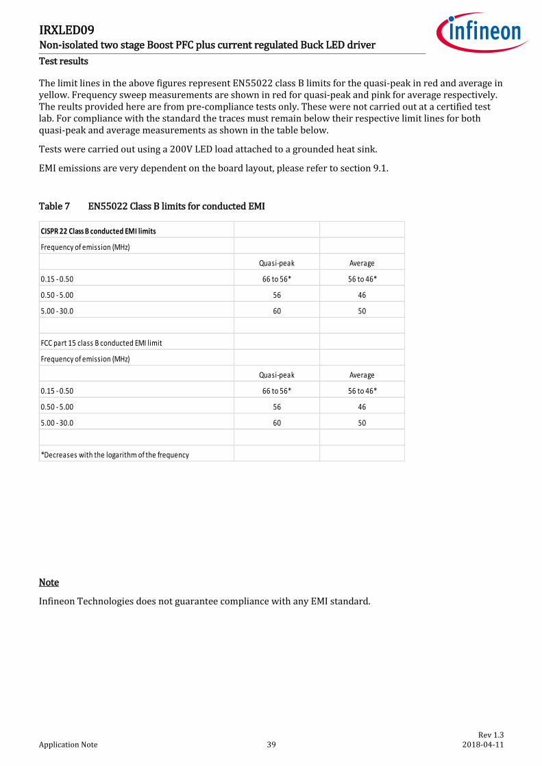
Test results
The limit lines in the above figures represent EN55022 class B limits for the quasi-peak in red and average in yellow. Frequency sweep measurements are shown in red for quasi-peak and pink for average respectively. The reults provided here are from pre-compliance tests only. These were not carried out at a certified test lab. For compliance with the standard the traces must remain below their respective limit lines for both quasi-peak and average measurements as shown in the table below.
Tests were carried out using a 200V LED load attached to a grounded heat sink.
EMI emissions are very dependent on the board layout, please refer to section 9.1.
Table 7 EN55022 Class B limits for conducted EMI
Note
Infineon Technologies does not guarantee compliance with any EMI standard.
CISPR 22 Class B conducted EMI limits
Frequency of emission (MHz)
Quasi-peak Average
0.15 - 0.50 66 to 56* 56 to 46*
0.50 - 5.00 56 46
5.00 - 30.0 60 50
FCC part 15 class B conducted EMI limit
Frequency of emission (MHz)
Quasi-peak Average
0.15 - 0.50 66 to 56* 56 to 46*
0.50 - 5.00 56 46
5.00 - 30.0 60 50
*Decreases with the logarithm of the frequency
Rev 1.3 Application Note 40 2018-04-11
IRXLED09 Non-isolated two stage Boost PFC plus current regulated Buck LED driver
Conclusion
11 Conclusion
The IRXLED09 evaluation board demonstrates a low cost two stage PFC plus CC Buck LED driver with both stages controlled by the low cost IRS2505L. It is shown that the IRS2505L may be configured for peak current regulation in a Buck converter operating in critical conduction mode. Accuracy of regulation over output voltage remains within +/-5% of the nominal output over a three to one voltage range.
Rapid start over the full range of AC line input with no power loss during steady state operation is demonstrated by means of the IRS25751 high voltage start-up IC, which may be replaced by resistors as a low cost alternative. The start-up time with the IRS25751 is approximately 250ms irrespective of input voltage, compared with approximately 500ms and 1s when resistors are used in place of it.
It is seen that current increases at reduced output voltage due to shorter duty cycle and the greater effect of propagation delay combined with higher ripple. The useful operating range for the converter has a 2.5 to 1 ratio of maximum to minimum voltage/power. This covers sufficient load range below which it would not make economic sense to use this LED driver.
Test results show that the design specifications are met.
References
[1] IRS2505LPBF SMPS control IC datasheet, Infineon Technologies.
[2] IRS25751LPBF High voltage start-up IC datasheet, Infineon Technologies.
[3] IRS2505L µPFC Control IC Design guide, Peter B. Green and Helen Ding, Infineon Technologies.
[4] AN-1214 LED Buck converter design using the IRS2505L, E. Bakalakos, Infineon Technologies (formerly International Rectifier)
[5] AN-1209 Using the IRS25751 high voltage start-up IC, T. Ribarich, Infineon Technologies (formerly International Rectifier)
Attention:
Revision History
Major changes since the last revision
Page or Reference Description of change
First Release
Rev 1.1 Minor corrections
Rev 1.2 Output capacitor COUT2 changed to 56uF/250V. CY1 and CY2 were increased to 2.2nF.
Schematic, test results and waveforms updated.

Trademarks of Infineon Technologies AG AURIX™, C166™, CanPAK™, CIPOS™, CoolGaN™, CoolMOS™, CoolSET™, CoolSiC™, CORECONTROL™, CROSSAVE™, DAVE™, DI-POL™, DrBlade™, EasyPIM™, EconoBRIDGE™, EconoDUAL™, EconoPACK™, EconoPIM™, EiceDRIVER™, eupec™, FCOS™, HITFET™, HybridPACK™, Infineon™, ISOFACE™, IsoPACK™, i-Wafer™, MIPAQ™, ModSTACK™, my-d™, NovalithIC™, OmniTune™, OPTIGA™, OptiMOS™, ORIGA™, POWERCODE™, PRIMARION™, PrimePACK™, PrimeSTACK™, PROFET™, PRO-SIL™, RASIC™, REAL3™, ReverSave™, SatRIC™, SIEGET™, SIPMOS™, SmartLEWIS™, SOLID FLASH™, SPOC™, TEMPFET™, thinQ!™, TRENCHSTOP™, TriCore™. Trademarks updated August 2015
Other Trademarks All referenced product or service names and trademarks are the property of their respective owners. ifx1owners.
Edition 2018-04-11
AppNote Number
UG_201705_PL16_05
Published by
Infineon Technologies AG
81726 Munich, Germany
© 2018 Infineon Technologies AG. All Rights Reserved.
Do you have a question about this document?
Email: [email protected]
Document reference
IMPORTANT NOTICE The information contained in this application note is given as a hint for the implementation of the product only and shall in no event be regarded as a description or warranty of a certain functionality, condition or quality of the product. Before implementation of the product, the recipient of this application note must verify any function and other technical information given herein in the real application. Infineon Technologies hereby disclaims any and all warranties and liabilities of any kind (including without limitation warranties of non-infringement of intellectual property rights of any third party) with respect to any and all information given in this application note. The data contained in this document is exclusively intended for technically trained staff. It is the responsibility of customer’s technical departments to evaluate the suitability of the product for the intended application and the completeness of the product information given in this document with respect to such application.
For further information on the product, technology, delivery terms and conditions and prices please contact your nearest Infineon Technologies office (www.infineon.com).
WARNINGS Due to technical requirements products may contain dangerous substances. For information on the types in question please contact your nearest Infineon Technologies office. Except as otherwise explicitly approved by Infineon Technologies in a written document signed by authorized representatives of Infineon Technologies, Infineon Technologies’ products may not be used in any applications where a failure of the product or any consequences of the use thereof can reasonably be expected to result in personal injury.

![Isolated AC-DC Converter with PFC - Vicor Corporation · Isolated AC-DC Converter with PFC PFM4914xB6M24D0yA Size: 4.91 x 1.40 x 0.37in [124.75 x 35.54 x 9.40mm] Part Ordering Information](https://img.pdfslide.us/doc/110x75/5e6bfa1c701c741c420c1688/isolated-ac-dc-converter-with-pfc-vicor-isolated-ac-dc-converter-with-pfc-pfm4914xb6m24d0ya.jpg)