Embed Size (px)
Citation preview
Digital ICIntroduction
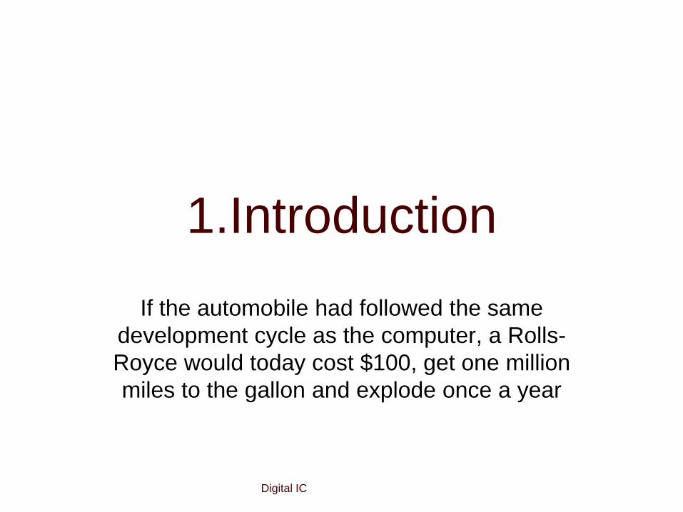
1.Introduction
If the automobile had followed the same
development cycle as the computer, a Rolls-
Royce would today cost $100, get one million
miles to the gallon and explode once a year
Digital IC
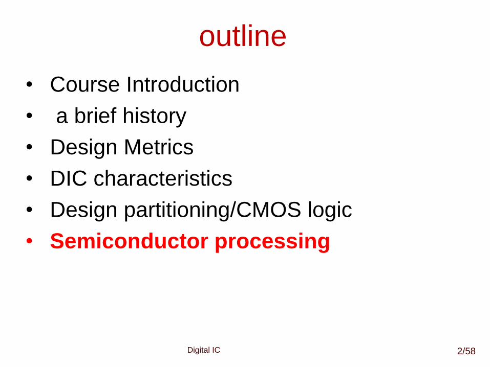
outline
• Course Introduction
• a brief history
• Design Metrics
• DIC characteristics
• Design partitioning/CMOS logic
• Semiconductor processing
2/58
Digital IC
Semiconductor processing
• Semiconductor fabrication
• Layout fundamental
• Semiconductor testing
• Semiconductor assembling
3/58
Digital IC
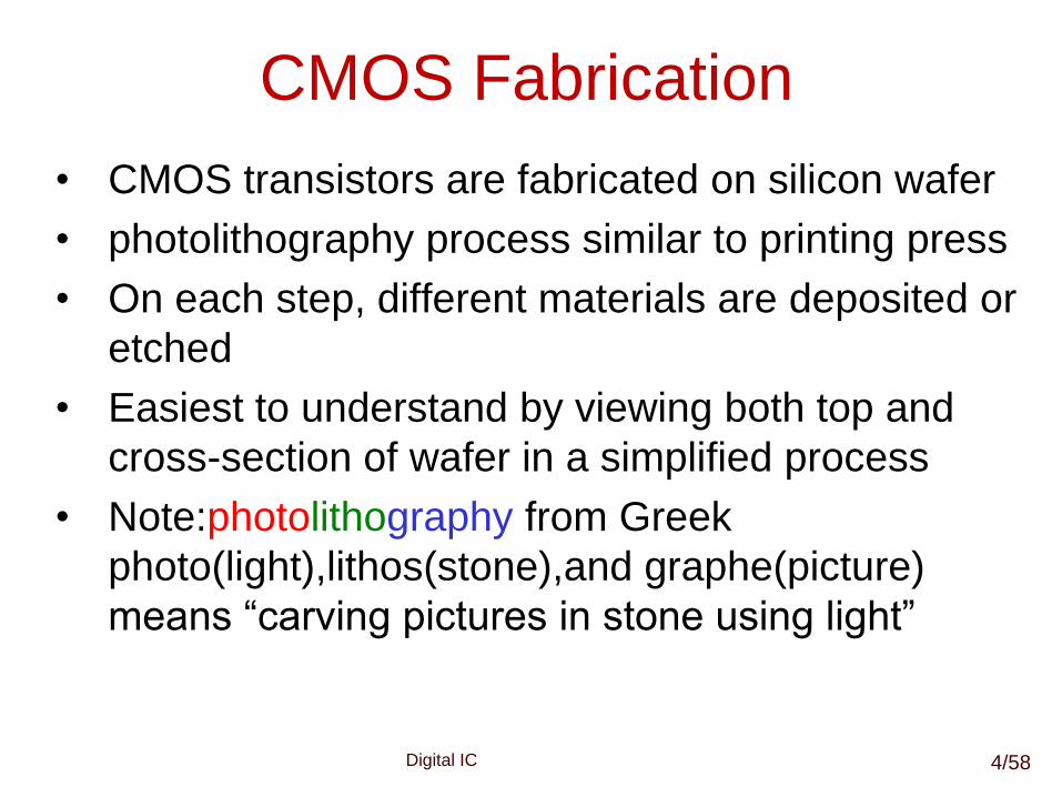
CMOS Fabrication
• CMOS transistors are fabricated on silicon wafer
• photolithography process similar to printing press
• On each step, different materials are deposited or
etched
• Easiest to understand by viewing both top and
cross-section of wafer in a simplified process
• Note:photolithography from Greek
photo(light),lithos(stone),and graphe(picture)
means “carving pictures in stone using light”
4/58
Digital IC
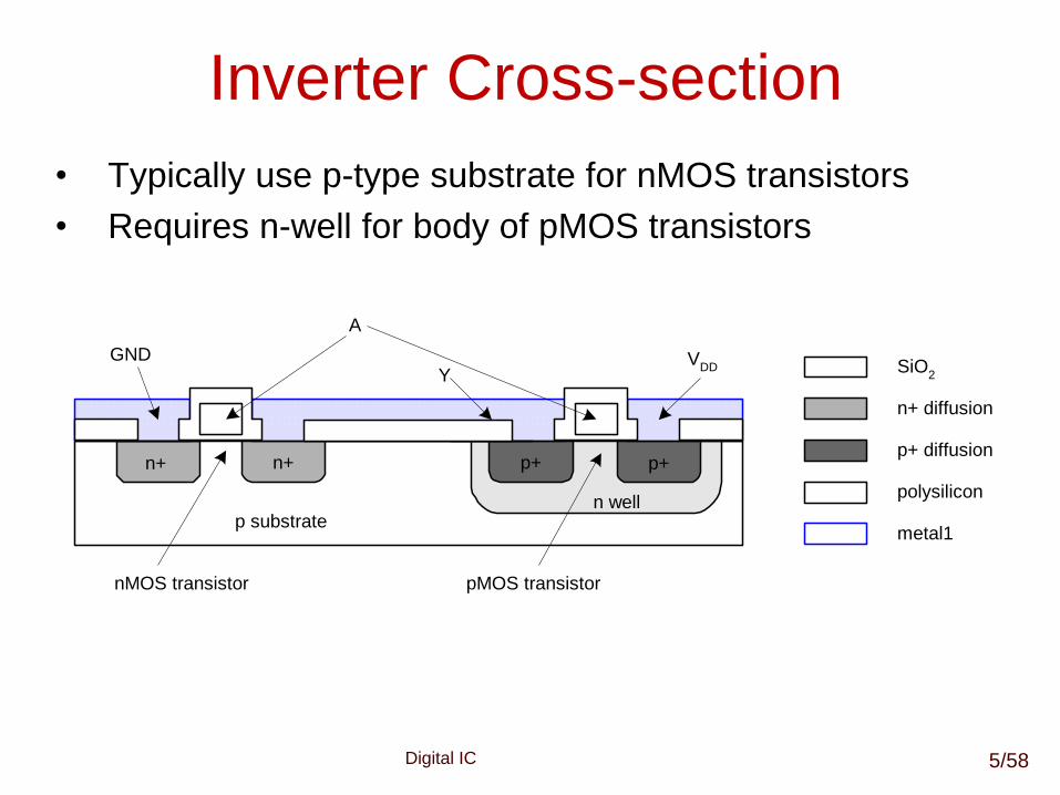
Inverter Cross-section
• Typically use p-type substrate for nMOS transistors
• Requires n-well for body of pMOS transistors
n+
p substrate
p+
n well
A
YGND V
DD
n+ p+
SiO2
n+ diffusion
p+ diffusion
polysilicon
metal1
nMOS transistor pMOS transistor
5/58
Digital IC
Well and Substrate Taps
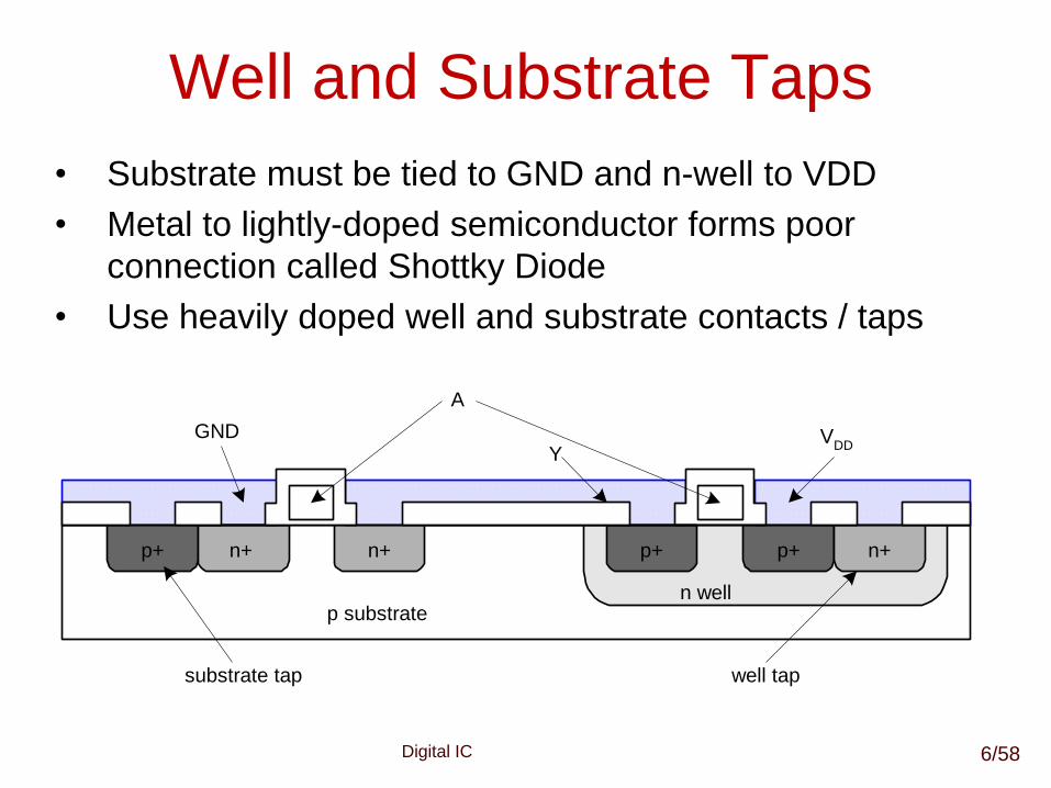
• Substrate must be tied to GND and n-well to VDD
• Metal to lightly-doped semiconductor forms poor
connection called Shottky Diode
• Use heavily doped well and substrate contacts / taps
n+
p substrate
p+
n well
A
YGND V
DD
n+p+
substrate tap well tap
n+ p+
6/58
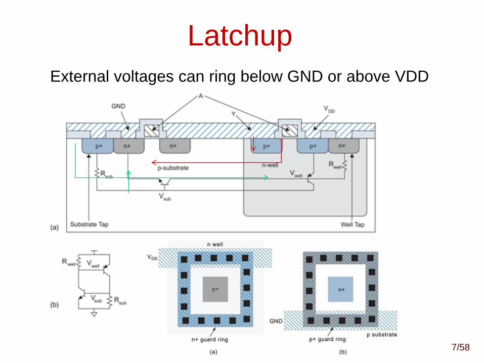
Digital IC
Latchup
External voltages can ring below GND or above VDD
7/58
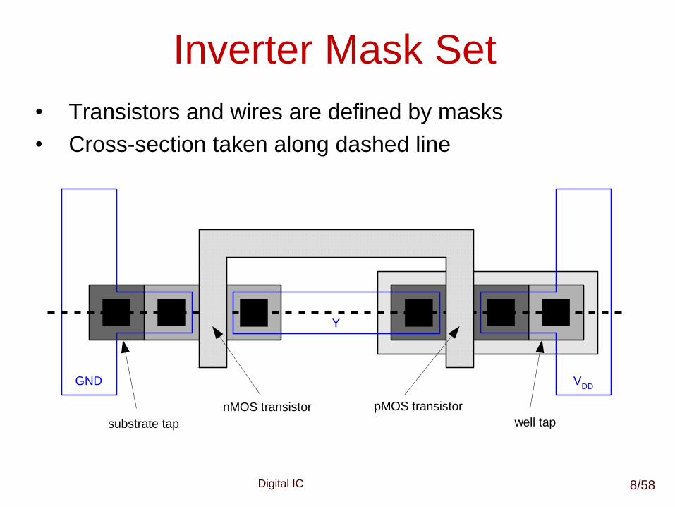
Digital IC
Inverter Mask Set
• Transistors and wires are defined by masks
• Cross-section taken along dashed line
GND VDD
Y
A
substrate tap well tap
nMOS transistor pMOS transistor
8/58
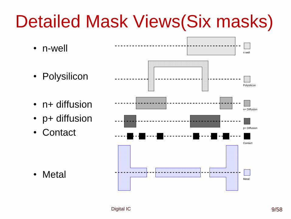
Digital IC
Detailed Mask Views(Six masks)
• n-well
• Polysilicon
• n+ diffusion
• p+ diffusion
• Contact
• MetalMetal
Polysilicon
Contact
n+ Diffusion
p+ Diffusion
n well
9/58
Digital IC
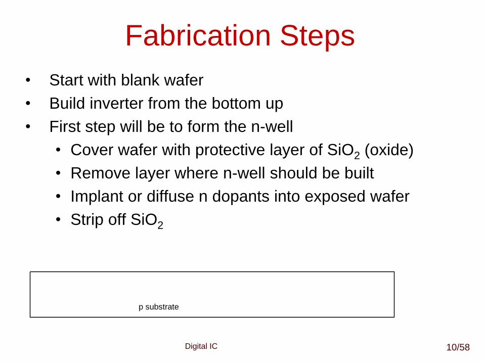
Fabrication Steps
• Start with blank wafer
• Build inverter from the bottom up
• First step will be to form the n-well
• Cover wafer with protective layer of SiO2 (oxide)
• Remove layer where n-well should be built
• Implant or diffuse n dopants into exposed wafer
• Strip off SiO2
p substrate
10/58
Digital IC
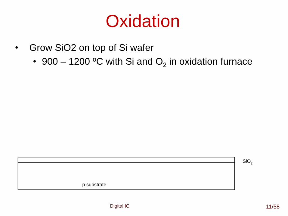
Oxidation
• Grow SiO2 on top of Si wafer
• 900 – 1200 ºC with Si and O2 in oxidation furnace
p substrate
SiO2
11/58
Digital IC
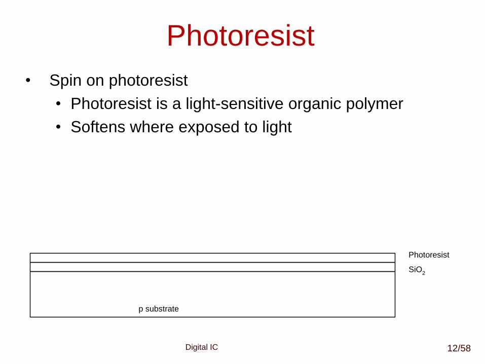
Photoresist
• Spin on photoresist
• Photoresist is a light-sensitive organic polymer
• Softens where exposed to light
p substrate
SiO2
Photoresist
12/58
Digital IC
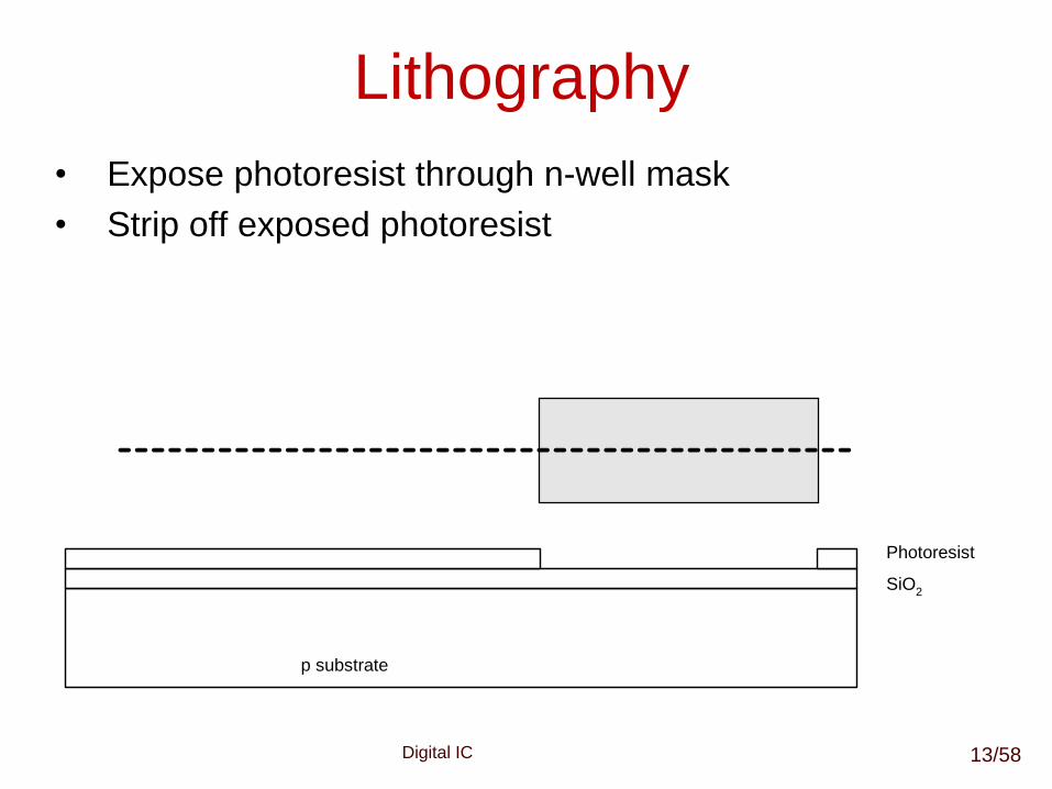
Lithography
• Expose photoresist through n-well mask
• Strip off exposed photoresist
p substrate
SiO2
Photoresist
13/58
Digital IC
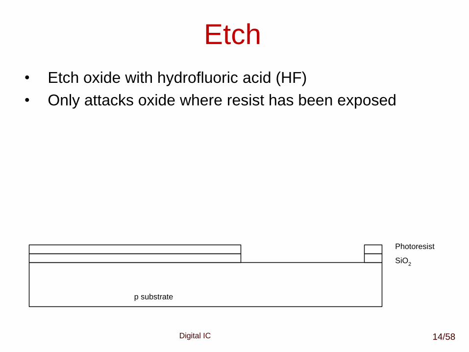
Etch
• Etch oxide with hydrofluoric acid (HF)
• Only attacks oxide where resist has been exposed
p substrate
SiO2
Photoresist
14/58
Digital IC
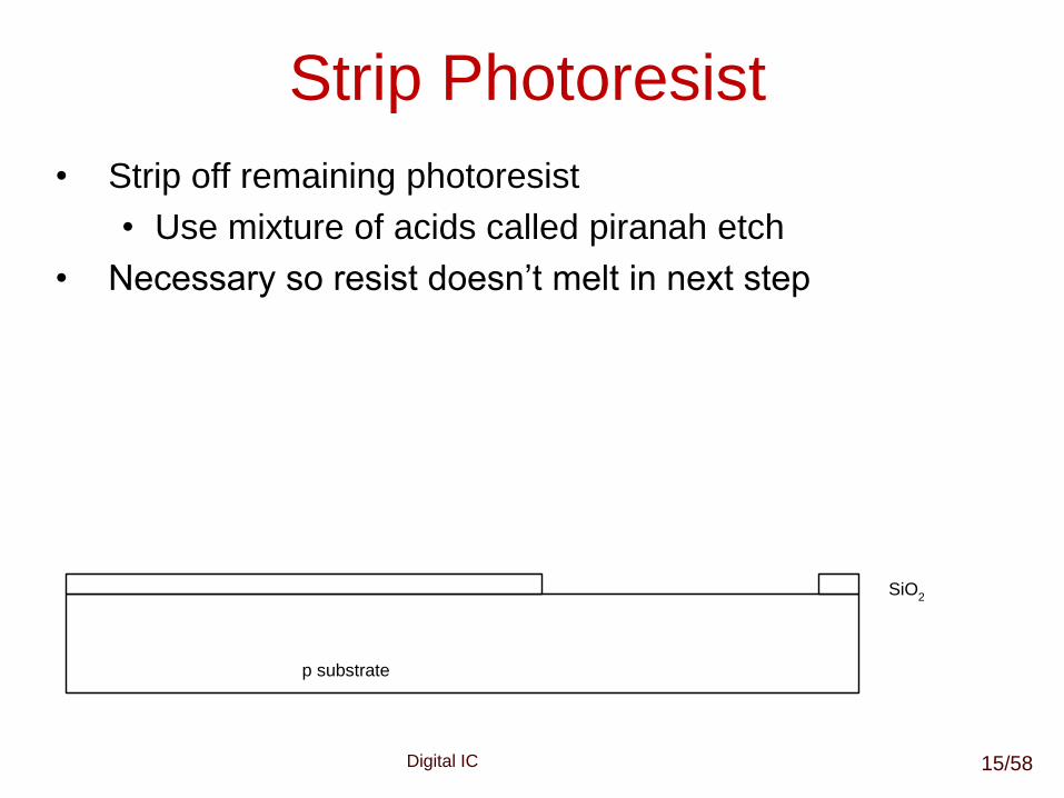
Strip Photoresist
• Strip off remaining photoresist
• Use mixture of acids called piranah etch
• Necessary so resist doesn’t melt in next step
p substrate
SiO2
15/58
Digital IC
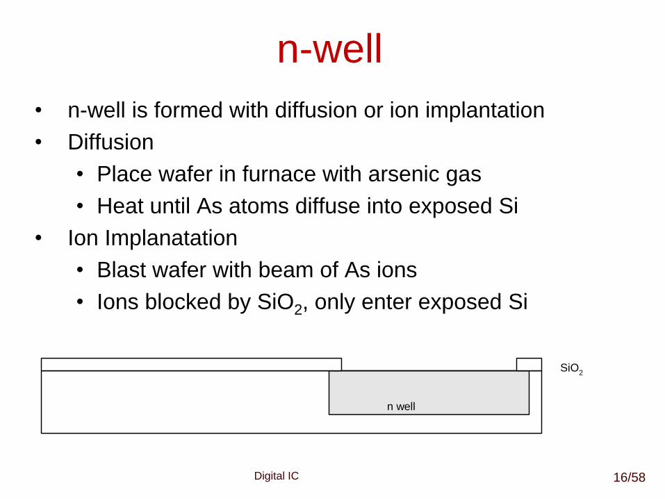
n-well
• n-well is formed with diffusion or ion implantation
• Diffusion
• Place wafer in furnace with arsenic gas
• Heat until As atoms diffuse into exposed Si
• Ion Implanatation
• Blast wafer with beam of As ions
• Ions blocked by SiO2, only enter exposed Si
n well
SiO2
16/58
Digital IC
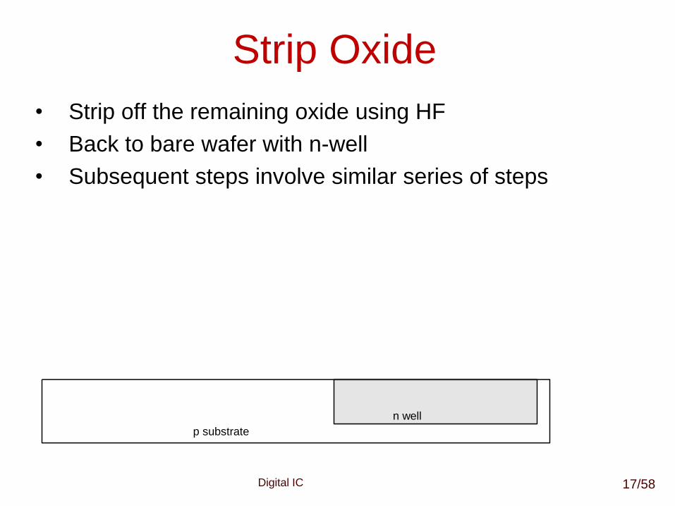
Strip Oxide
• Strip off the remaining oxide using HF
• Back to bare wafer with n-well
• Subsequent steps involve similar series of steps
p substrate
n well
17/58
Digital IC
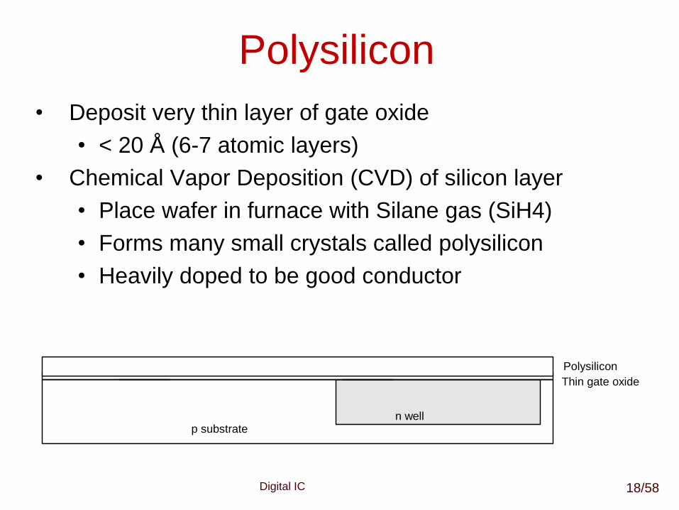
Polysilicon
• Deposit very thin layer of gate oxide
• < 20 Å (6-7 atomic layers)
• Chemical Vapor Deposition (CVD) of silicon layer
• Place wafer in furnace with Silane gas (SiH4)
• Forms many small crystals called polysilicon
• Heavily doped to be good conductor
Thin gate oxide
Polysilicon
p substraten well
18/58
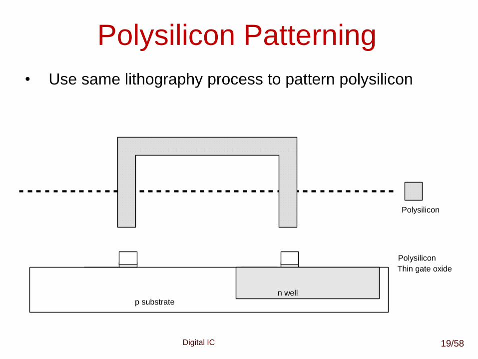
Digital IC
Polysilicon Patterning
• Use same lithography process to pattern polysilicon
Polysilicon
p substrate
Thin gate oxide
Polysilicon
n well
19/58
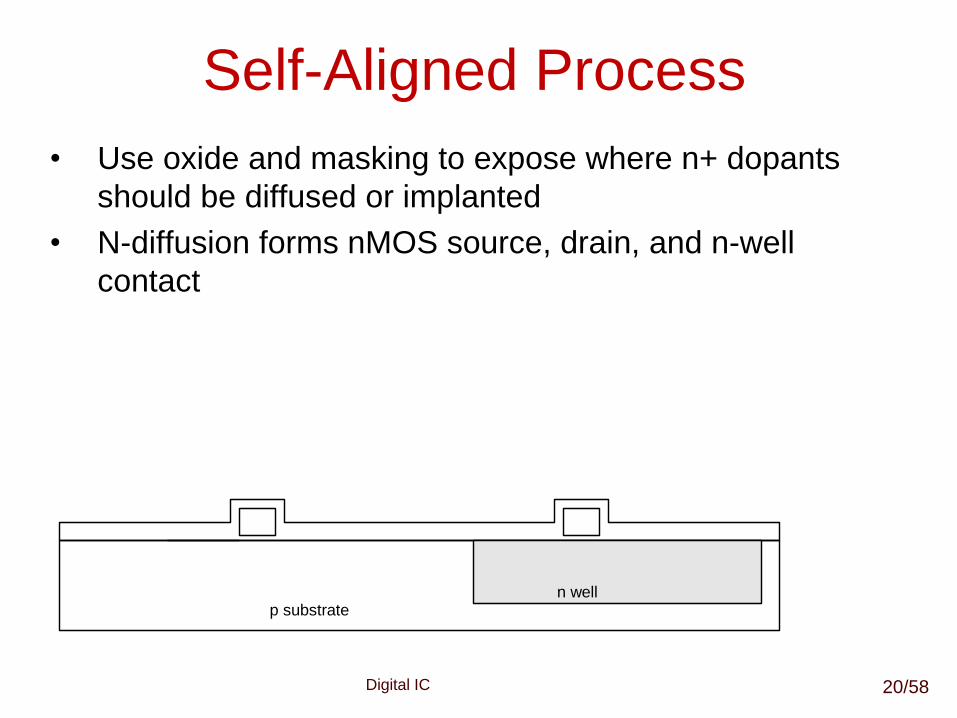
Digital IC
Self-Aligned Process
• Use oxide and masking to expose where n+ dopants
should be diffused or implanted
• N-diffusion forms nMOS source, drain, and n-well
contact
p substraten well
20/58
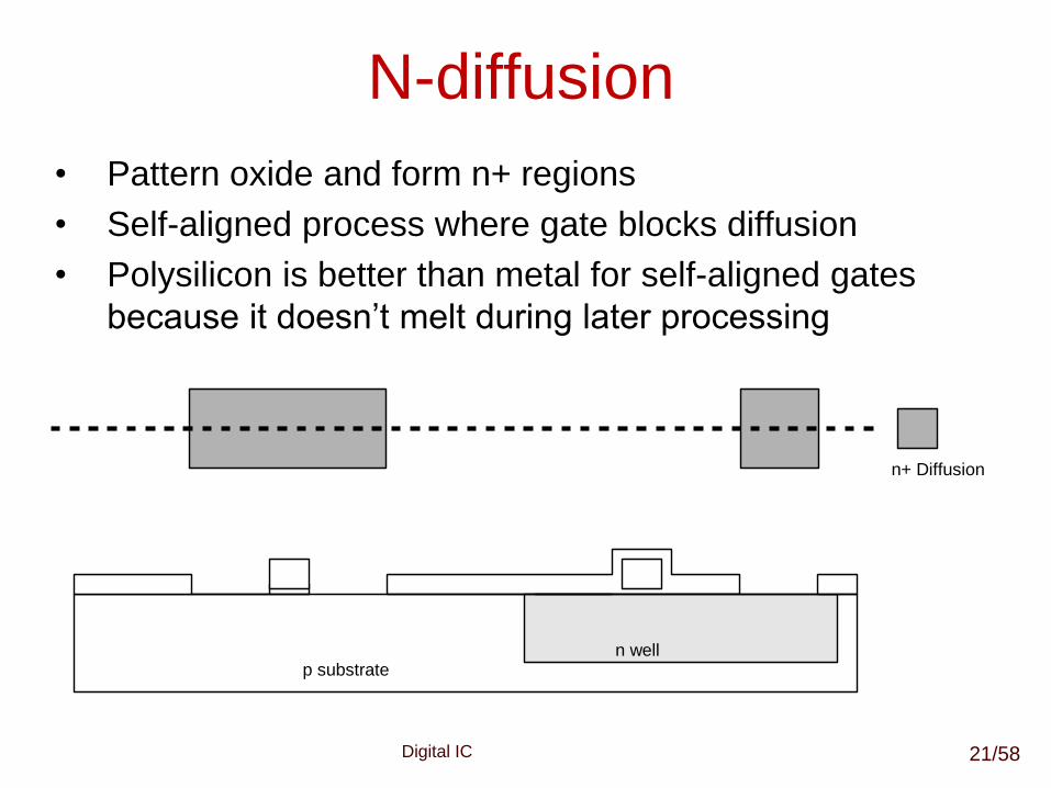
Digital IC
N-diffusion
• Pattern oxide and form n+ regions
• Self-aligned process where gate blocks diffusion
• Polysilicon is better than metal for self-aligned gates
because it doesn’t melt during later processing
p substraten well
n+ Diffusion
21/58
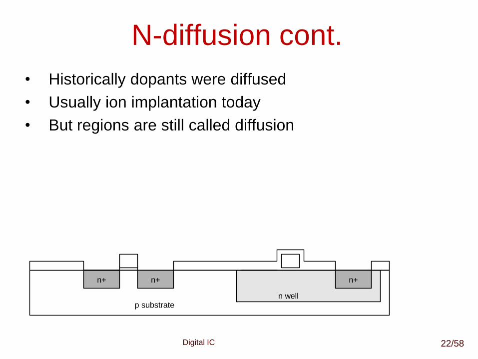
Digital IC
N-diffusion cont.
• Historically dopants were diffused
• Usually ion implantation today
• But regions are still called diffusion
n wellp substrate
n+n+ n+
22/58
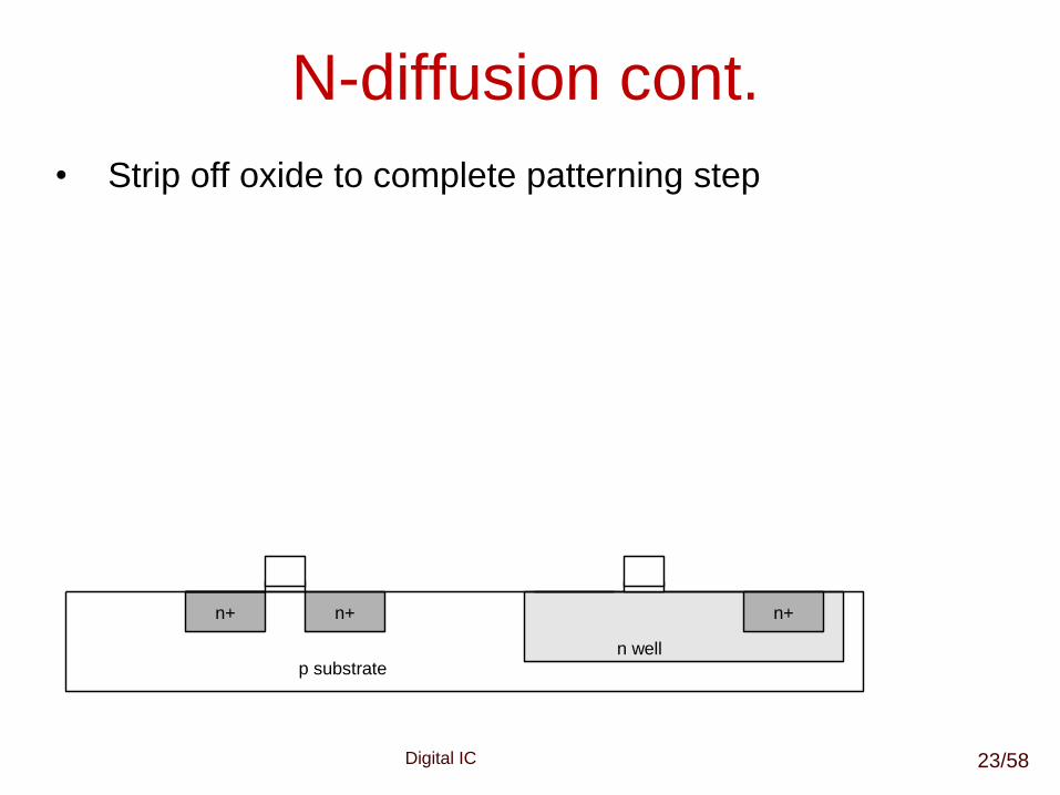
Digital IC
N-diffusion cont.
• Strip off oxide to complete patterning step
n wellp substrate
n+n+ n+
23/58
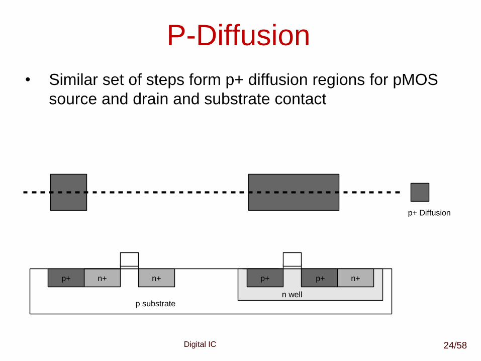
Digital IC
P-Diffusion
• Similar set of steps form p+ diffusion regions for pMOS
source and drain and substrate contact
p+ Diffusion
p substraten well
n+n+ n+p+p+p+
24/58
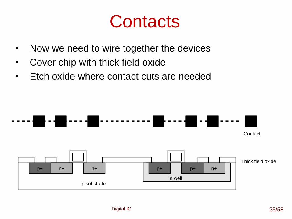
Digital IC
Contacts
• Now we need to wire together the devices
• Cover chip with thick field oxide
• Etch oxide where contact cuts are needed
p substrate
Thick field oxide
n well
n+n+ n+p+p+p+
Contact
25/58
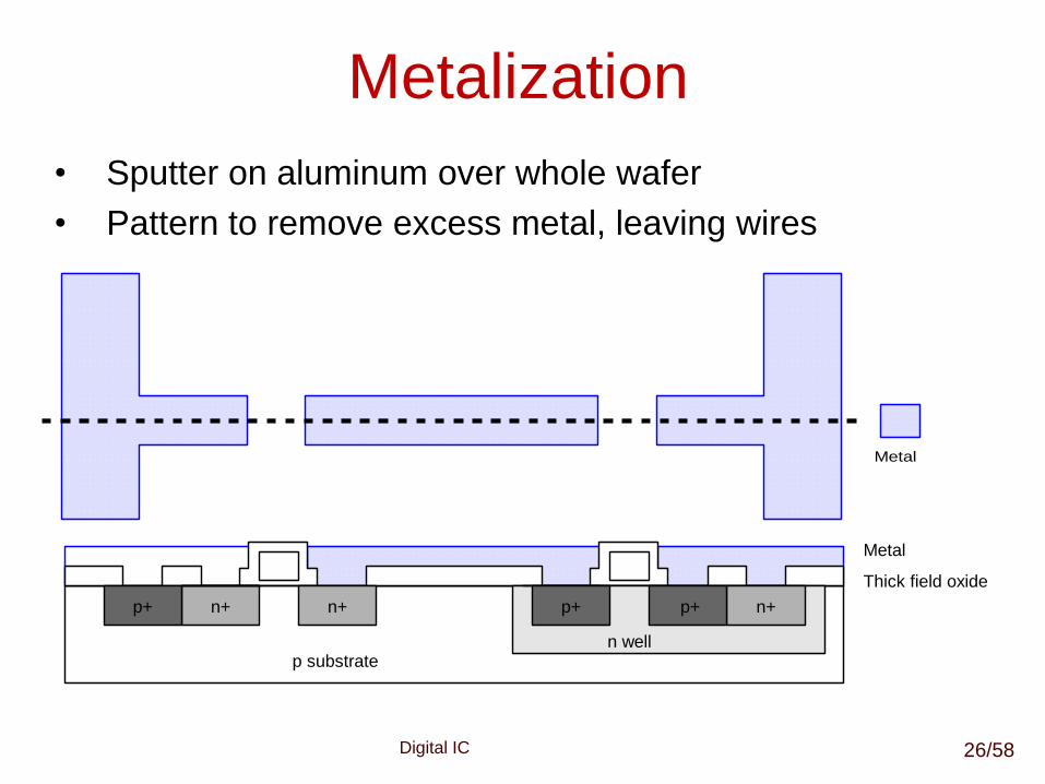
Digital IC
Metalization
• Sputter on aluminum over whole wafer
• Pattern to remove excess metal, leaving wires
p substrate
Metal
Thick field oxide
n well
n+n+ n+p+p+p+
Metal
26/58
Digital IC
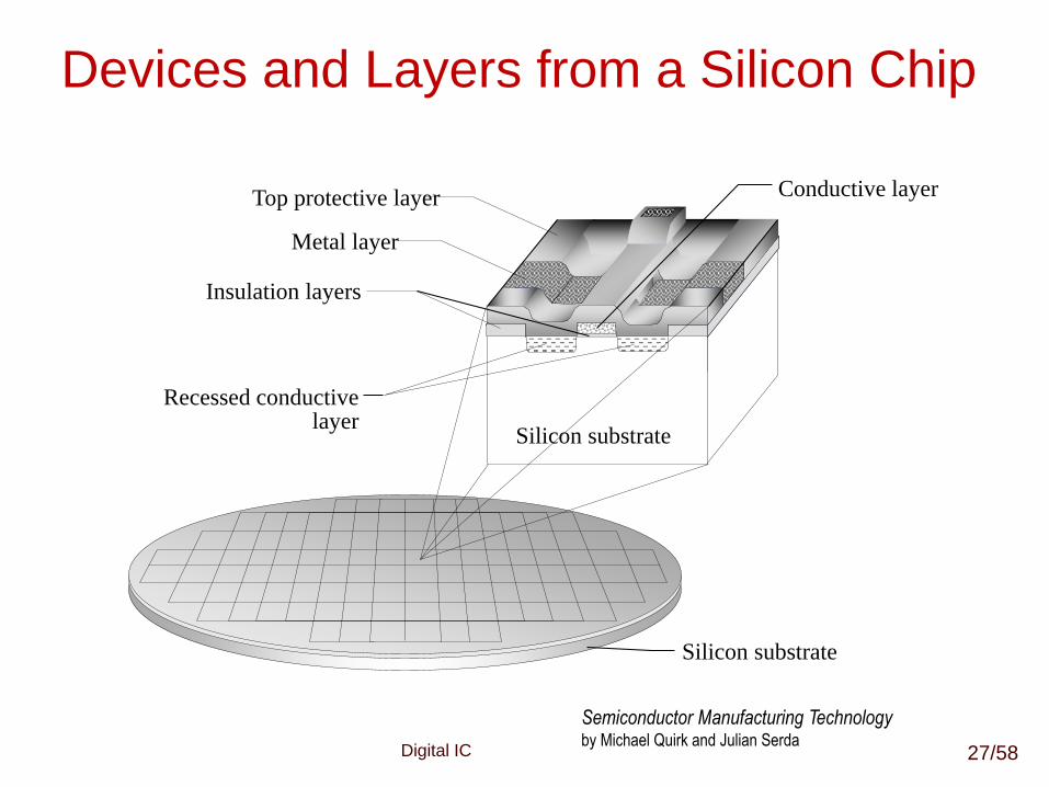
Devices and Layers from a Silicon Chip
Silicon substrate
drain
Silicon substrate
Top protective layer
Metal layer
Insulation layers
Recessed conductive layer
Conductive layer
Semiconductor Manufacturing Technologyby Michael Quirk and Julian Serda
27/58
Digital IC
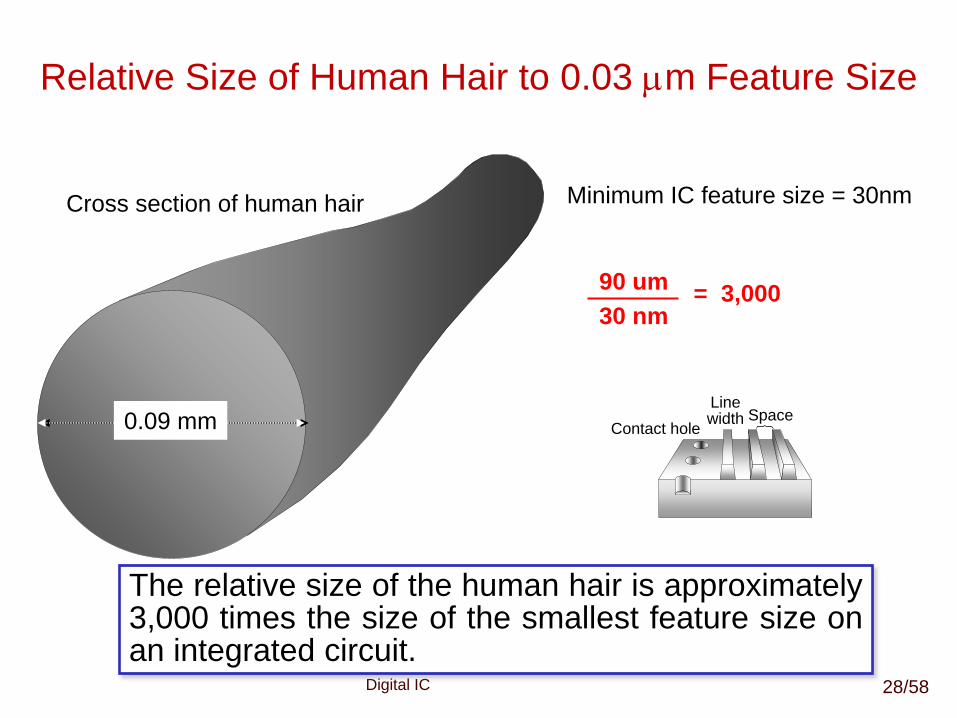
Relative Size of Human Hair to 0.03 mm Feature Size
Contact hole
Line width Space0.09 mm
Minimum IC feature size = 30nm
The relative size of the human hair is approximately3,000 times the size of the smallest feature size onan integrated circuit.
Cross section of human hair
90 um
30 nm= 3,000
28/58
Digital IC
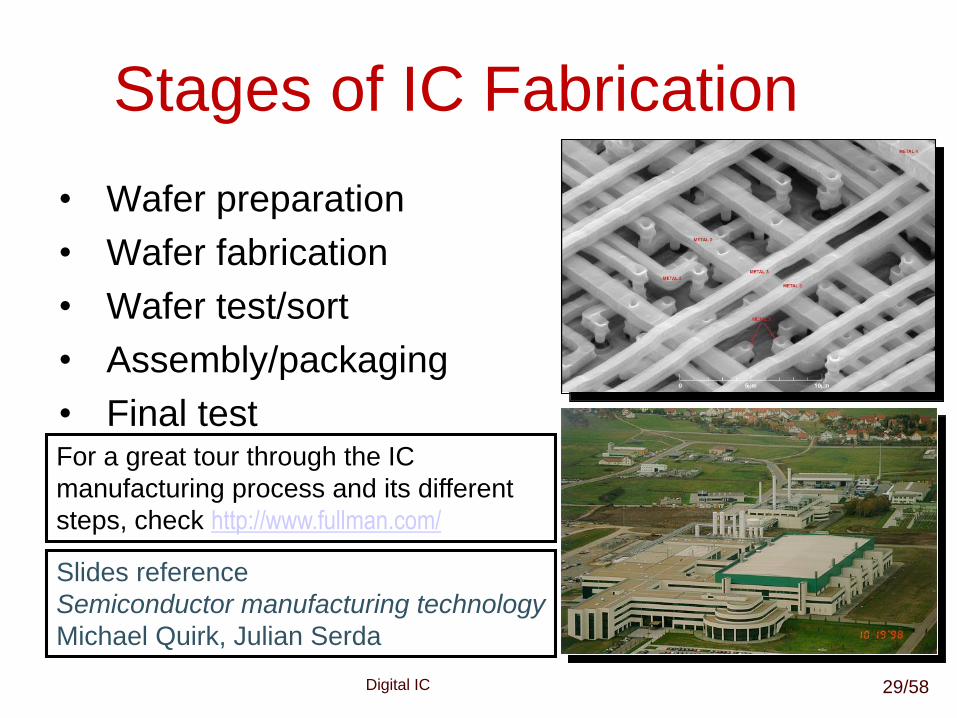
Stages of IC Fabrication
• Wafer preparation
• Wafer fabrication
• Wafer test/sort
• Assembly/packaging
• Final testFor a great tour through the IC
manufacturing process and its different
steps, check http://www.fullman.com/
Slides reference
Semiconductor manufacturing technology
Michael Quirk, Julian Serda
29/58
Digital IC
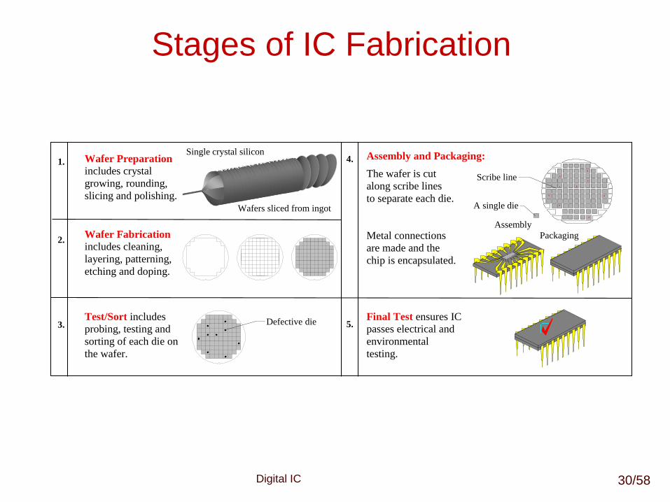
Stages of IC Fabrication
Wafer Preparation includes crystal
growing, rounding,
slicing and polishing.
Assembly and Packaging:
The wafer is cut
along scribe lines
to separate each die.
Metal connections
are made and the
chip is encapsulated.
Wafer Fabrication includes cleaning,
layering, patterning,
etching and doping.
Test/Sort includes
probing, testing and
sorting of each die on
the wafer.
Final Test ensures IC
passes electrical and
environmental
testing.
Defective die
1.
2.
3.
Scribe line
A single die
Assembly
Packaging
4.
5.
Wafers sliced from ingot
Single crystal silicon
30/58
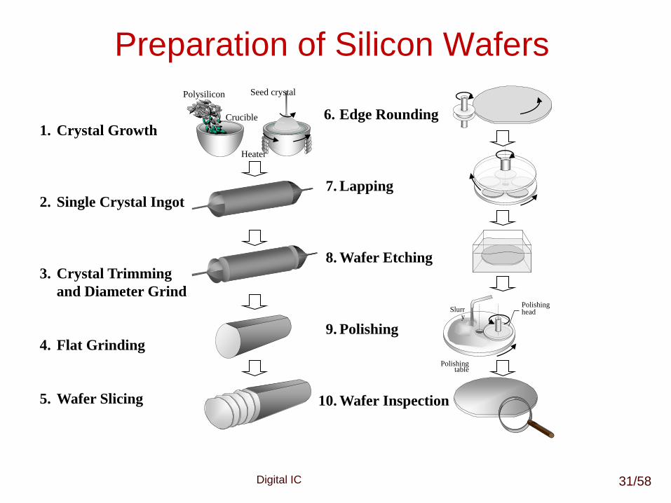
Digital IC
Preparation of Silicon Wafers
1. Crystal Growth
2. Single Crystal Ingot
3. Crystal Trimming
and Diameter Grind
4. Flat Grinding
5. Wafer Slicing
6. Edge Rounding
7. Lapping
8. Wafer Etching
9. Polishing
10. Wafer Inspection
Slurry
Polishing table
Polishing head
Polysilicon Seed crystal
Heater
Crucible
31/58
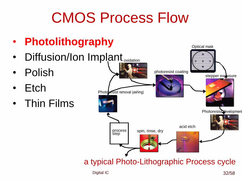
Digital IC
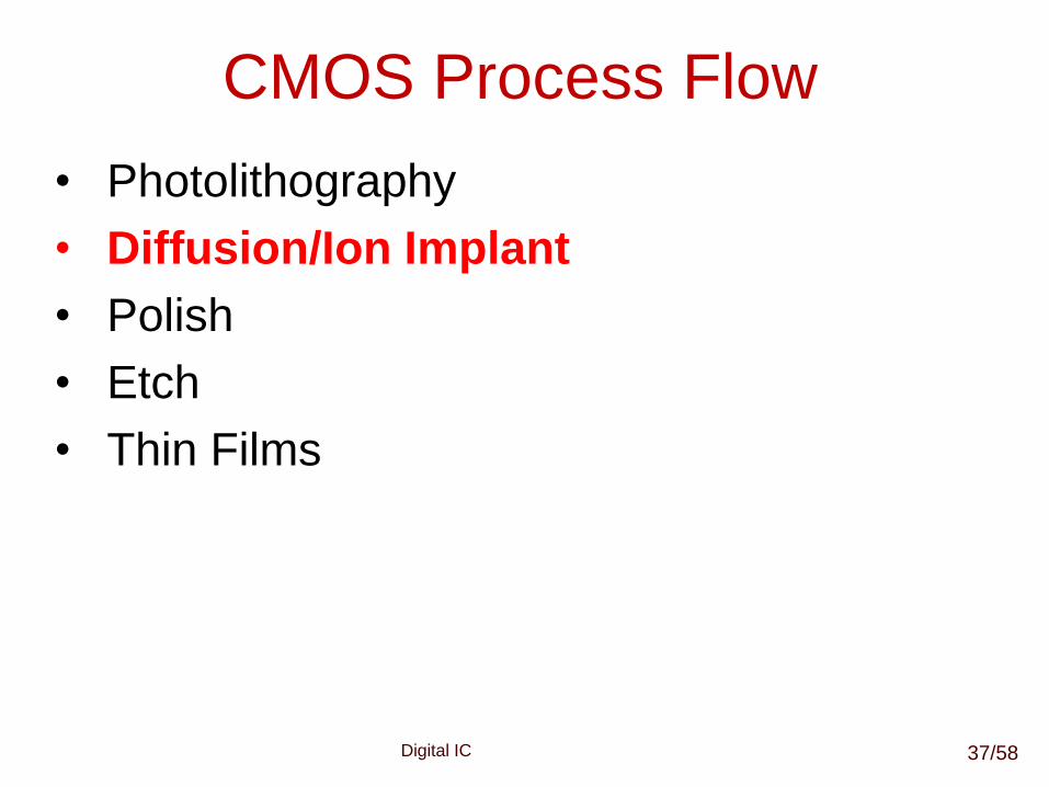
CMOS Process Flow
• Photolithography
• Diffusion/Ion Implant
• Polish
• Etch
• Thin Films
oxidation
Optical mask
processstep
photoresist coating
Photoresist removal (ashing)
spin, rinse, dryacid etch
Photoresist development
stepper exposure
a typical Photo-Lithographic Process cycle
32/58
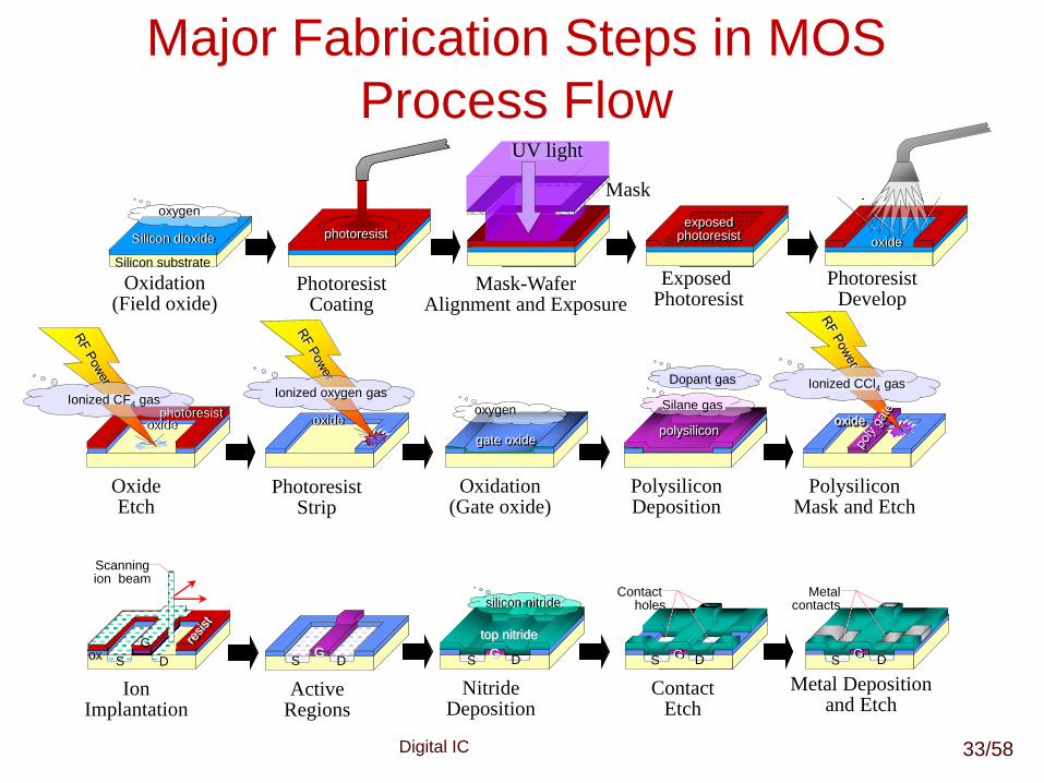
Digital IC
Major Fabrication Steps in MOS
Process Flow
Oxidation(Field oxide)
Silicon substrate
Silicon dioxide
oxygen
PhotoresistDevelop
oxide
PhotoresistCoating
photoresist
Mask-WaferAlignment and Exposure
Mask
UV light
Exposed Photoresist
exposedphotoresist
GS D
Active Regions
top nitride
S DG
silicon nitride
NitrideDeposition
Contact holes
S DG
ContactEtch
Ion Implantation
oxD
G
Scanning ion beam
S
Metal Deposition and Etch
drainS DG
Metal contacts
PolysiliconDeposition
polysilicon
Silane gas
Dopant gas
Oxidation(Gate oxide)
gate oxide
oxygen
PhotoresistStrip
oxide
Ionized oxygen gas
OxideEtch
photoresistoxide
Ionized CF4 gas
PolysiliconMask and Etch
oxide
Ionized CCl4 gas
33/58
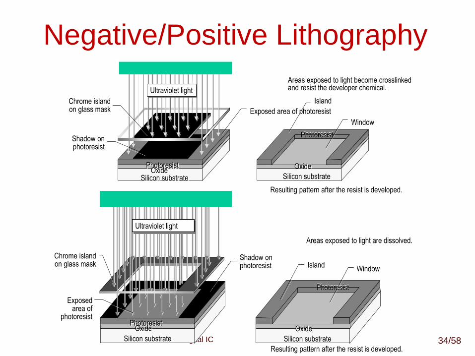
Digital IC
Negative/Positive Lithography
Ultraviolet light
Island
Areas exposed to light become crosslinked and resist the developer chemical.
Resulting pattern after the resist is developed.
Window
Exposed area of photoresist
Shadow on photoresist
Chrome island on glass mask
Silicon substrate
PhotoresistOxide
Photoresist
Oxide
Silicon substrate
photoresist
silicon substrate
oxide oxidesilicon substrate
photoresist
Ultraviolet light
Island
Areas exposed to light are dissolved.
Resulting pattern after the resist is developed.
Shadow on photoresist
Exposed area of
photoresist
Chrome island on glass mask
Window
Silicon substrate
PhotoresistOxide
Photoresist
Oxide
Silicon substrate 34/58
Digital IC
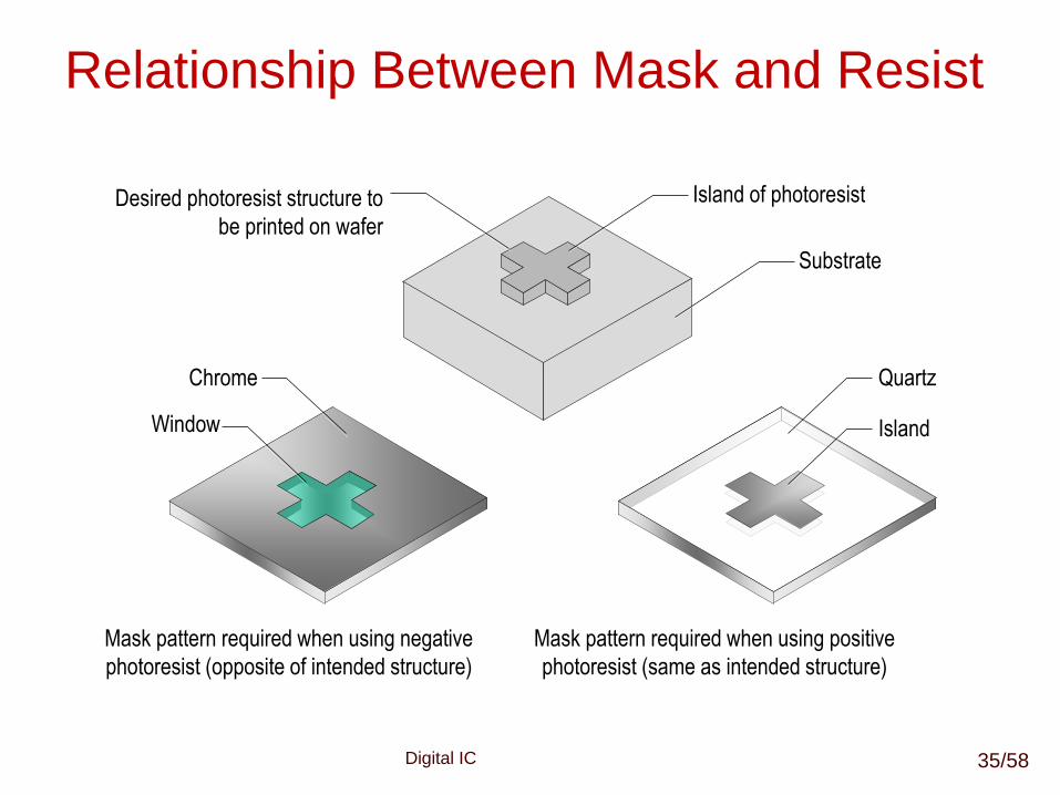
Relationship Between Mask and Resist
Desired photoresist structure to
be printed on wafer
Window
Substrate
Island of photoresist
QuartzChrome
Island
Mask pattern required when using negative
photoresist (opposite of intended structure)
Mask pattern required when using positive
photoresist (same as intended structure)
35/58
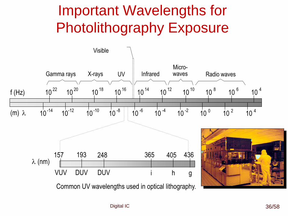
Digital IC
Important Wavelengths for
Photolithography Exposure
Visible
Radio wavesMicro-wavesInfraredGamma rays UVX-rays
f (Hz) 1010101010101010 10104681012141622 1820
(m) 420-2-4-6-8-14 -10-121010101010101010 1010
365 436405248193157
ghiDUVDUVVUV
(nm)
Common UV wavelengths used in optical lithography.
36/58
Digital IC
CMOS Process Flow
• Photolithography
• Diffusion/Ion Implant
• Polish
• Etch
• Thin Films
37/58
Digital IC
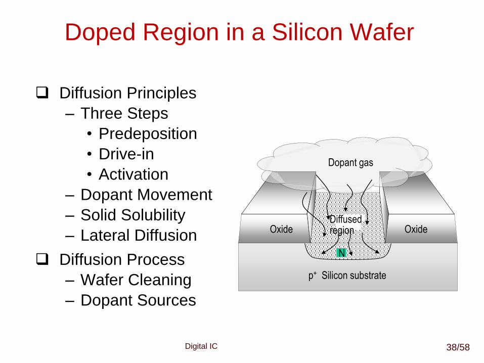
Doped Region in a Silicon Wafer
OxideOxide
p+ Silicon substrate
Dopant gas
N
Diffused region
Diffusion Principles
– Three Steps
• Predeposition
• Drive-in
• Activation
– Dopant Movement
– Solid Solubility
– Lateral Diffusion
Diffusion Process
– Wafer Cleaning
– Dopant Sources
38/58
Digital IC
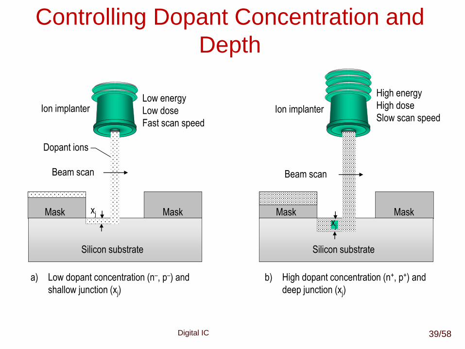
Controlling Dopant Concentration and
Depth
a) Low dopant concentration (n–, p–) and
shallow junction (xj)
MaskMask
Silicon substrate
xj
Low energy
Low dose
Fast scan speed
Beam scan
Dopant ions
Ion implanter
b) High dopant concentration (n+, p+) and
deep junction (xj)
Beam scan
High energy
High dose
Slow scan speed
MaskMask
Silicon substrate
xj
Ion implanter
39/58
Digital IC
CMOS Process Flow
• Photolithography
• Diffusion/Ion Implant
• Polish/Etch
• Thin Films
40/58
Digital IC
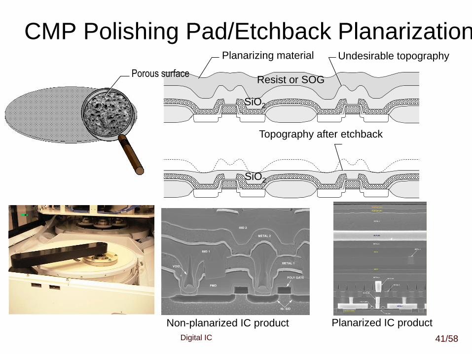
CMP Polishing Pad/Etchback Planarization
SiO2
Topography after etchback
Resist or SOG
SiO2
Planarizing material Undesirable topography
Non-planarized IC product Planarized IC product
Porous surface
41/58
Digital IC
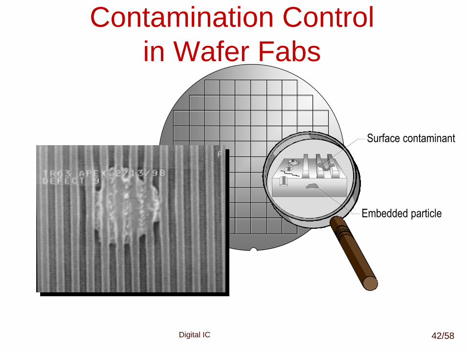
Contamination Control
in Wafer Fabs
Embedded particle
Surface contaminant
42/58
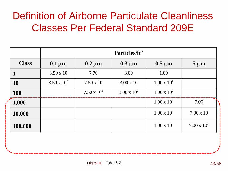
Digital IC
Definition of Airborne Particulate Cleanliness
Classes Per Federal Standard 209E
Table 6.2
Particles/ft3
Class 0.1 mm 0.2 mm 0.3 mm 0.5 mm 5 mm
1 3.50 x 10 7.70 3.00 1.00
10 3.50 x 10² 7.50 x 10 3.00 x 10 1.00 x 101
100 7.50 x 10² 3.00 x 10² 1.00 x 10²
1,000 1.00 x 10³ 7.00
10,000 1.00 x 10⁴ 7.00 x 10
100,000 1.00 x 10⁵ 7.00 x 10²
43/58
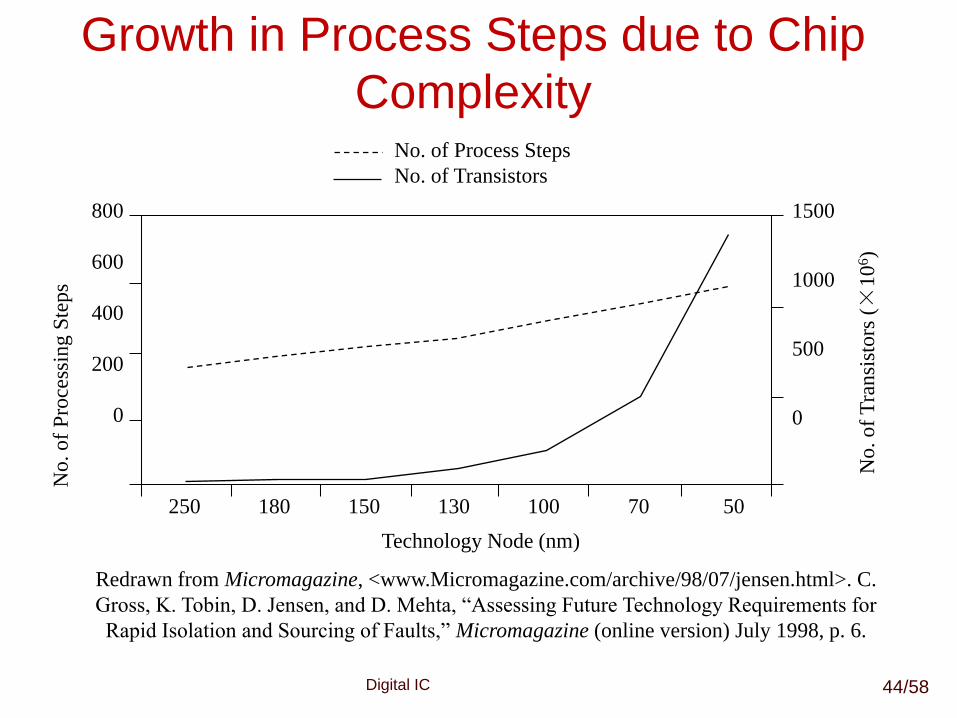
Digital IC
Growth in Process Steps due to Chip
Complexity
800
600
400
200
0
1500
1000
500
0
250 180 150 130 100 70 50
No. of Process Steps
No. of Transistors
Technology Node (nm)
No. of
Pro
cess
ing
Ste
ps
No. of
Tra
nsi
sto
rs (×
10
6)
Redrawn from Micromagazine, <www.Micromagazine.com/archive/98/07/jensen.html>. C.
Gross, K. Tobin, D. Jensen, and D. Mehta, “Assessing Future Technology Requirements for
Rapid Isolation and Sourcing of Faults,” Micromagazine (online version) July 1998, p. 6.
44/58
Digital IC
Semiconductor processing
• Semiconductor fabrication
• Layout fundamental
• Semiconductor testing
• Semiconductor assembling
45/58
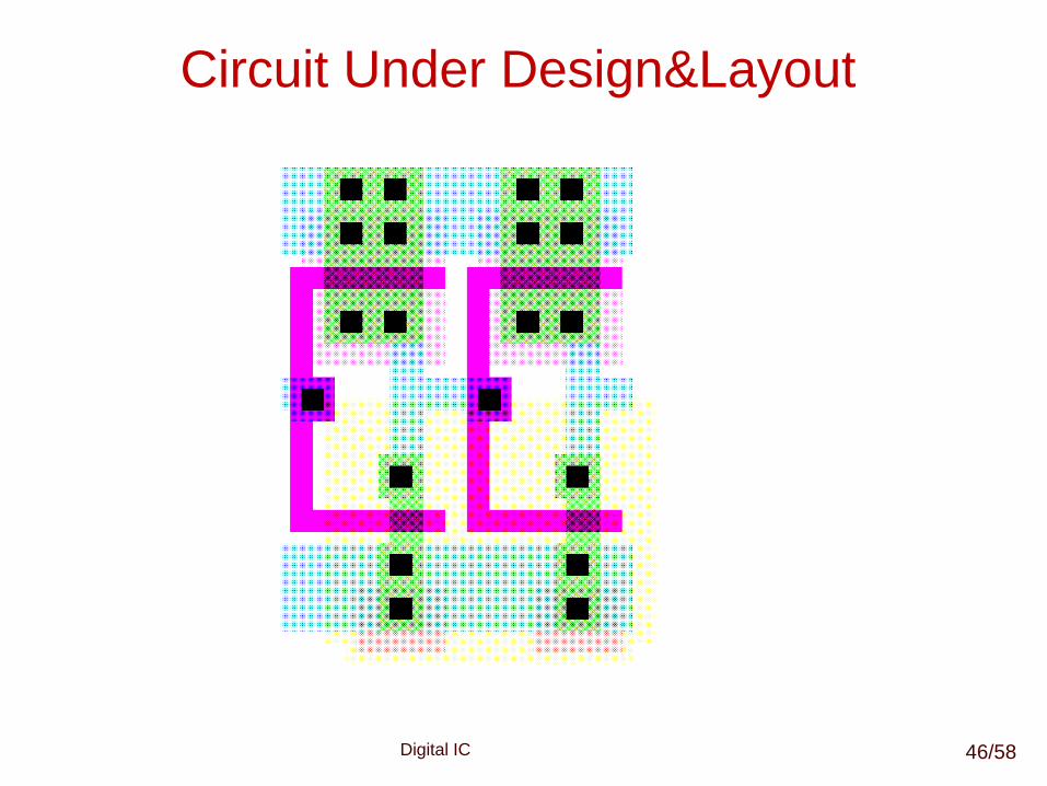
Digital IC
Circuit Under Design&Layout
46/58
Digital IC
Gate Layout
• Layout can be very time consuming
• Design gates to fit together nicely
• Build a library of standard cells
• Standard cell design methodology
• VDD and GND should abut (standard height)
• Adjacent gates should satisfy design rules
• nMOS at bottom and pMOS at top
• All gates include well and substrate contacts
47/58
Digital IC
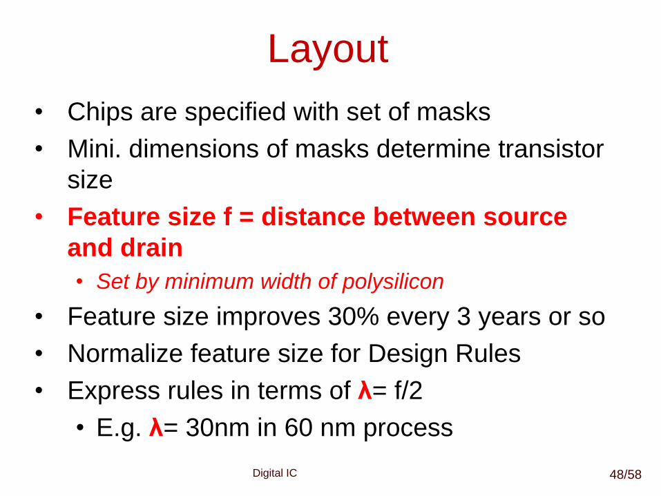
Layout
• Chips are specified with set of masks
• Mini. dimensions of masks determine transistor
size
• Feature size f = distance between source
and drain
• Set by minimum width of polysilicon
• Feature size improves 30% every 3 years or so
• Normalize feature size for Design Rules
• Express rules in terms of λ= f/2
• E.g. λ= 30nm in 60 nm process
48/58
Digital IC
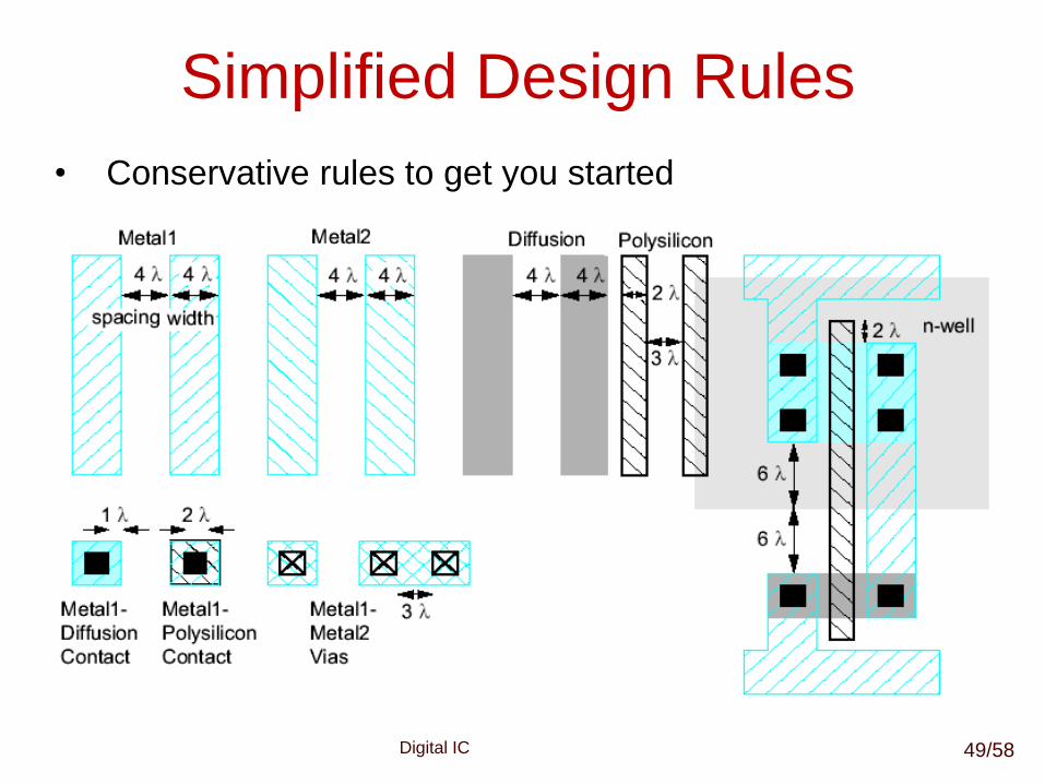
Simplified Design Rules
• Conservative rules to get you started
49/58
Digital IC
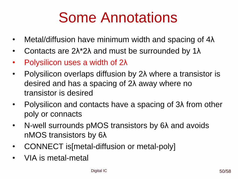
Some Annotations
• Metal/diffusion have minimum width and spacing of 4λ
• Contacts are 2λ*2λ and must be surrounded by 1λ
• Polysilicon uses a width of 2λ
• Polysilicon overlaps diffusion by 2λ where a transistor is
desired and has a spacing of 2λ away where no
transistor is desired
• Polysilicon and contacts have a spacing of 3λ from other
poly or connacts
• N-well surrounds pMOS transistors by 6λ and avoids
nMOS transistors by 6λ
• CONNECT is[metal-diffusion or metal-poly]
• VIA is metal-metal
50/58
Digital IC
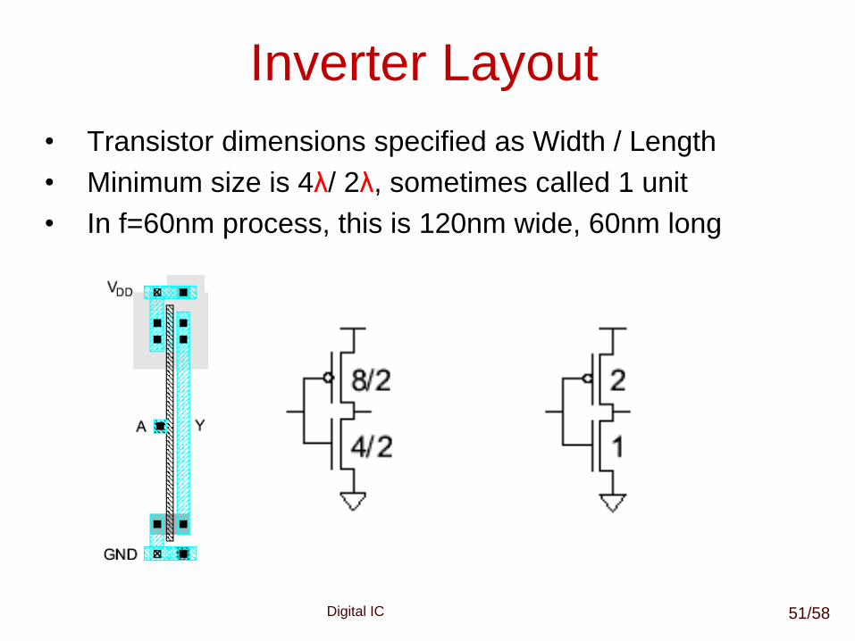
Inverter Layout
• Transistor dimensions specified as Width / Length
• Minimum size is 4λ/ 2λ, sometimes called 1 unit
• In f=60nm process, this is 120nm wide, 60nm long
51/58
Digital IC
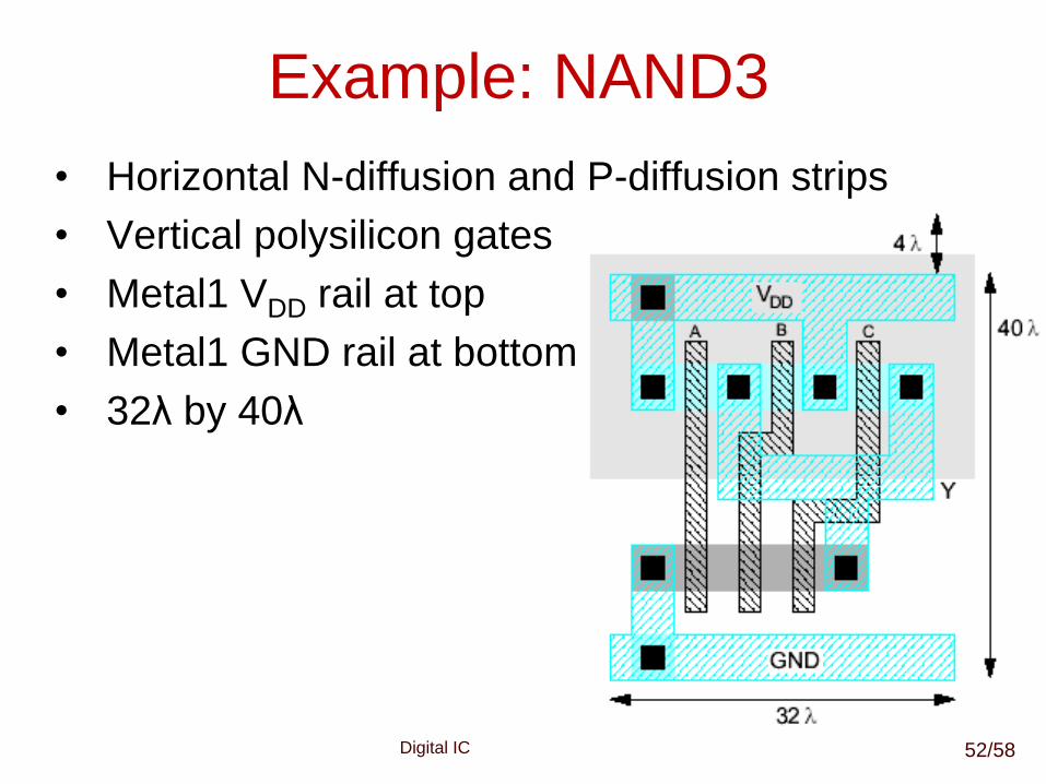
Example: NAND3
• Horizontal N-diffusion and P-diffusion strips
• Vertical polysilicon gates
• Metal1 VDD rail at top
• Metal1 GND rail at bottom
• 32λ by 40λ
52/58
Digital IC
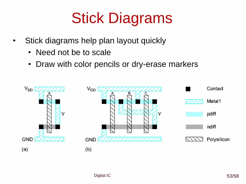
Stick Diagrams
• Stick diagrams help plan layout quickly
• Need not be to scale
• Draw with color pencils or dry-erase markers
53/58
Digital IC
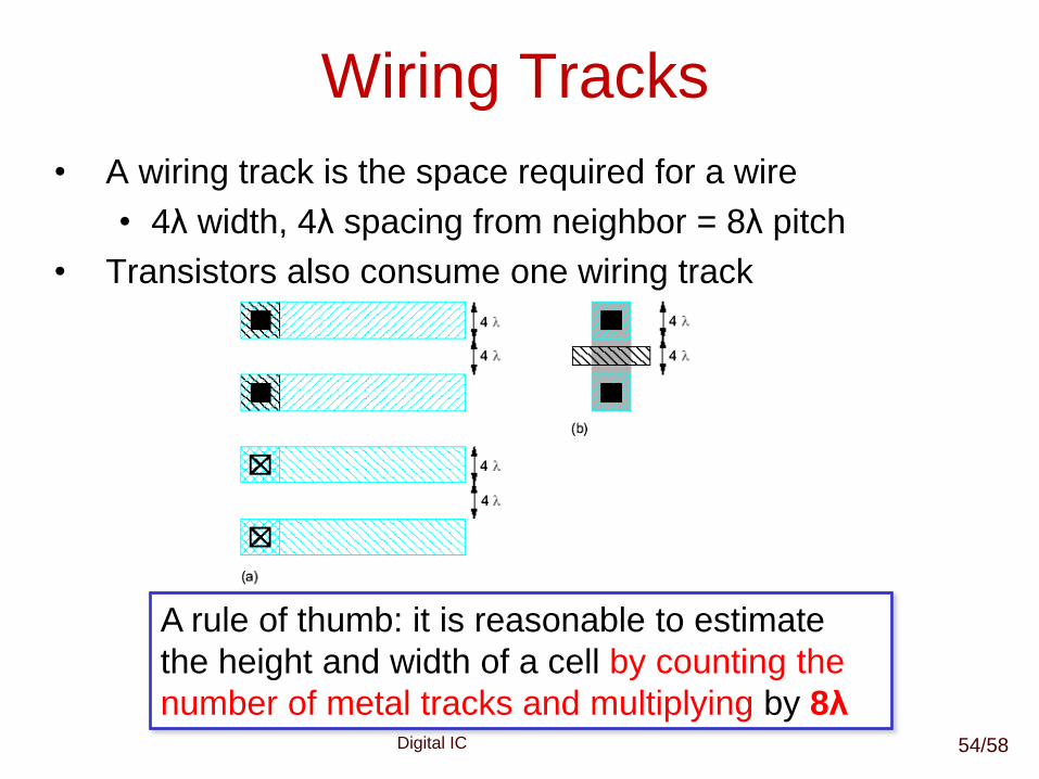
Wiring Tracks
• A wiring track is the space required for a wire
• 4λ width, 4λ spacing from neighbor = 8λ pitch
• Transistors also consume one wiring track
A rule of thumb: it is reasonable to estimate
the height and width of a cell by counting the
number of metal tracks and multiplying by 8λ54/58
Digital IC
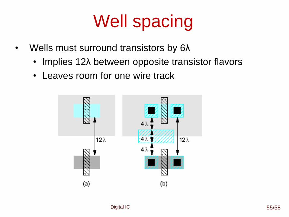
Well spacing
• Wells must surround transistors by 6λ
• Implies 12λ between opposite transistor flavors
• Leaves room for one wire track
55/58
Digital IC
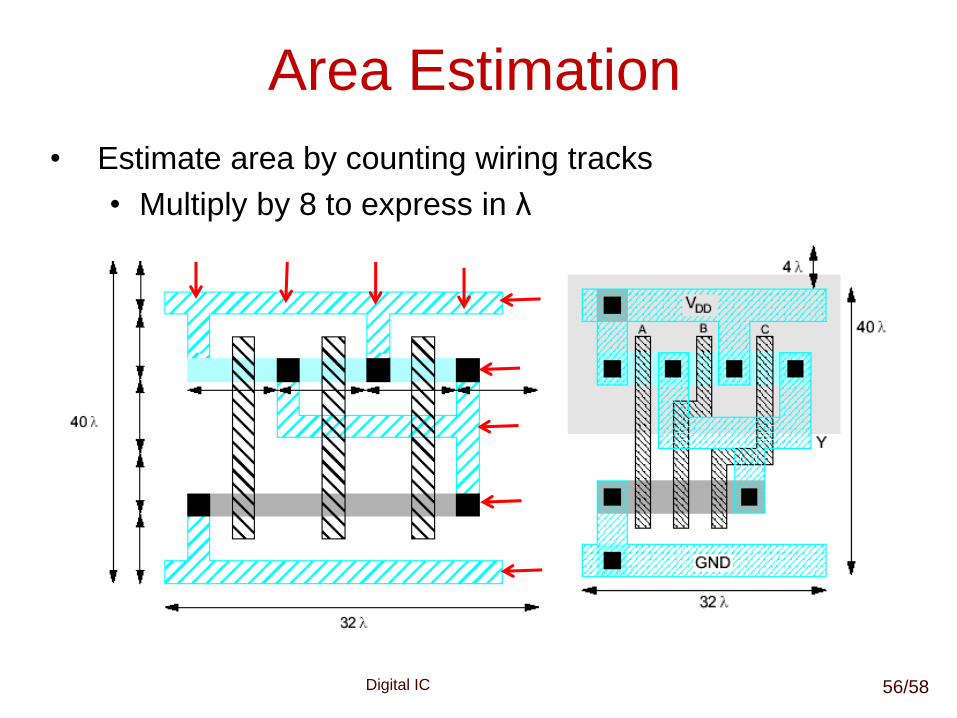
Area Estimation
• Estimate area by counting wiring tracks
• Multiply by 8 to express in λ
56/58
Digital IC
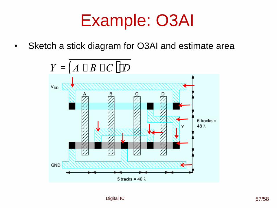
Example: O3AI
• Sketch a stick diagram for O3AI and estimate area
Y = A + B +C( )iD
57/58
Digital IC
tricky for horizontal size
• Diffusion should be counted as a wire
• If no wire between pMOS and nMOS,additional
track of wire still should be counted
• A track should be counted between VDD and the
next metal line
• If the transistors are wider than 4λ, the extra
width should be factored into the area estimate
58/58