Embed Size (px)
Citation preview

Tampere City
• The second largest city, often called “Manchester of Finland”
• > 220,000 inhabitants
• It is likely (according to press release, 2011) that Tampere is the fastest growing urban area.
• Two universities: Tampere University of Technology (Foundation), and the (classical) University of Tampere, totalling 30 000 students
1
28.11.2011
St. Petersburg, 15.11.2011

2
28.11.2011
Tampere University of Technology (TUT)
• Established in 1965
• TUT Foundation since 2010
• 10,400 students (2010)
• Collaboration with 200 universities around the world
• Funding = 138 M€ in 2010
St. Petersburg, 15.11.2011

Research at the international leading edge
Leading-edge fields of research:
• Nano-photonics, particularly epitaxial growth of
III-V’s & laser technology
• Signal processing
• Intelligent machines
Plus: Centres of Excellence in Research appointed by the Academy of Finland: Signal Processing Algorithm Research Group (SPAG) together with Generic Intelligent Machines Research (GIM) of Helsinki University of Technology
3
28.11.2011
Optoelectronics Research Centre – ORC / TUT
Intelligent Machines & Materials Research / TUT
St. Petersburg, 15.11.2011

Long-term basic research in high technology may lead to new products
Photonics and Modern Imaging Techniques
4
Nano-technology research Optoelectronics Research Centre - ORC
N
A
N
O
T
E
C
H
N
O
L
O
G
Y
Semiconductor technology • molecular beam epitaxy (MBE) of III-V
semiconductors (5 commercial MBE’s) • ultra-fast and high power lasers • Solar cells, one is on board an ESA’s satellite
(Equator-S)
Surface science • nano-structured metals and semiconductors • surface-environmental interactions • functionalized surfaces (for catalysis & corrosion)
Nano-photonics • Nano-imprint lithography (or NIL) • plasmonics
St. Petersburg, 15.11.2011
MBE SYSTEM
Multi-technique ESCA + STM
III-V quantum dots. Notice the regular pattern

Long-term basic research in high technology may lead to new products
Photonics and Modern Imaging Techniques
Nanochemistry for functional materials Laboratory of Chemistry at Department of Chemistry and Bio-engineering
-0.1 0.0 0.1 0.2 0.3 0.4 0.5 0.6
-16
-12
-8
-4
0
4
8
12
Alq3
ZnBT2
Alq3|ZnBT
2
JS
C,
mA
/cm
2
U, V
Organized molecular structures
• Mono molecular organic films
• Alternating organic molecular layers
• Self-assembled molecular structures
• Metal and semiconductor nano-particles
• Functionalized nano-particles
Phenomena studied in molecular structures
• Photo-physics of excited state
• Energy transfer
• Photo-induced electron transfer
• Photo-induced vectorial charge transfer
• Charge transport in organic structures
• Function of all organic solar cells
Synthesis Fabrication of thin-films
Organic Solar Cells prepared in
open air, functioning with the
efficiency of 6.7 %
St. Petersburg, 15.11.2011

Nano-technology Research
TUT Department of Physics
Aerosol physics
• Nanoparticle and nanopowder generation up to 1 g/min
• Functional nanocoatings in large scale
• Aerosol measurement, detection, instrumentation, 1 nm to 10 µm
• Traceable aerosol particle number concentration standard (5-1000 nm)
Optics: non-linear nano-photonics
• Supercontinuum and broadband sources
• Electromagnetic localization
• Nonlinear metamaterials
• Microscopy of nano-objects
Computational physics
• Unlocking ways of how lipids modulate membrane protein function
• Development of drugs for treatment of cardiovascular diseases
• Polymer coatings for optimizing optical and mechanical properties of
solid materials
• Functionalization of nanocellulose

Long-term basic research in high technology may lead to new products
Photonics and Modern Imaging Techniques
7
22.2.2010
Fundamental research and business in opto-electronics
Markus Pessa, ORC / TUT, Finland
St. Petersburg, 15.11.2011
Oulu
Joensuu
Helsinki
Tampere
Turku
SWEDEN FINLAND RUSSIA
ORC / TUT: 85 workers in 2011 Budget: 6 million euro / annum Investment in instruments: 37 M US$ Main products: (i) Epitaxial crystals growned by MBE; and (ii) semiconductor & (iii) fibre lasers
8
22.2.2010
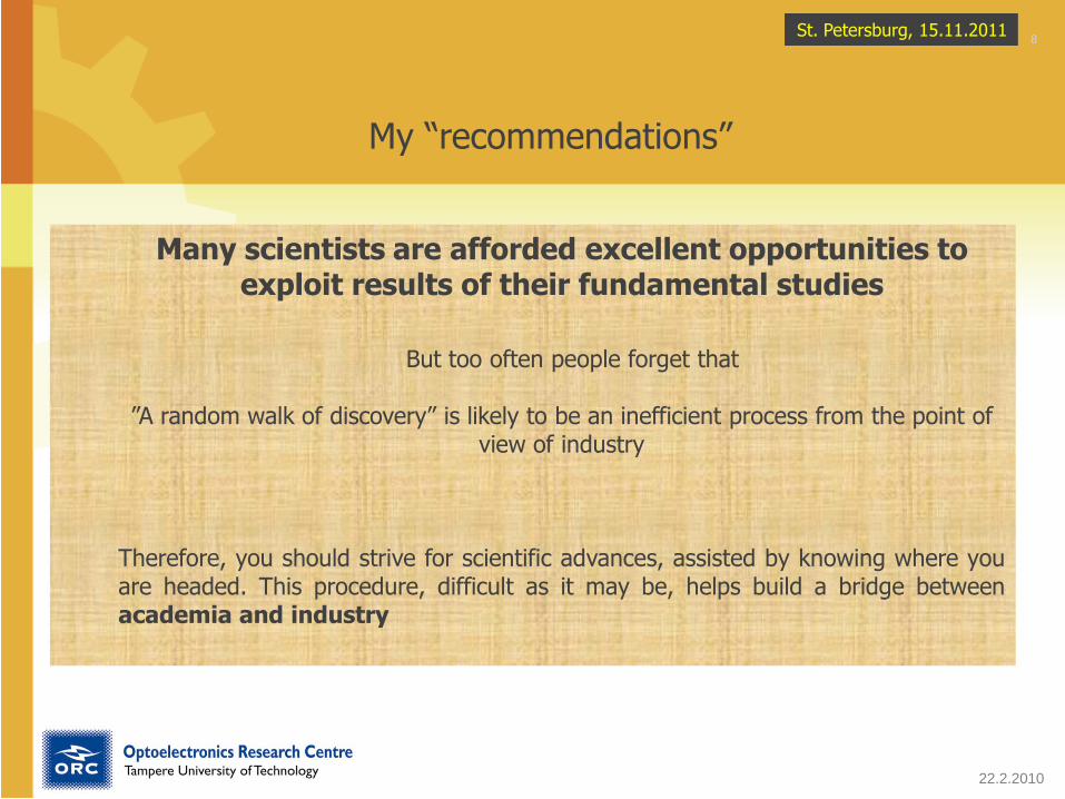
Many scientists are afforded excellent opportunities to exploit results of their fundamental studies
But too often people forget that ”A random walk of discovery” is likely to be an inefficient process from the point of
view of industry
Therefore, you should strive for scientific advances, assisted by knowing where you are headed. This procedure, difficult as it may be, helps build a bridge between academia and industry
My “recommendations”
St. Petersburg, 15.11.2011

9
Photonics companies in Finland are largely created as spin-offs from ORC / TUT
A million-dollar question is how to establish a company which would utilize your scientific observations commercially
I’ll show you how we did
St. Petersburg, 15.11.2011

10
22.2.2010
Coherent Finland Owned by Coherent Inc., Santa Clara, since 2002.
Products:
Epitaxial wafers by MBE and semiconductor lasers
Epitaxial III-V semiconductor wafers by Coherent Finland for commercial use by MBE
VECSELs (Semiconductor Disk Lasers), 976 nm
FAP – Coherent turn-key diode system for industrial applications; 100 < P < 1 kW
St. Petersburg, 15.11.2011
Coherent Finland moved to Santa Clara, California, in 2010 and sold all these buildings to Corelase (2010). So, Corelase moved in (2011)

11
22.2.2010
St. Petersburg, 15.10.2011
O-lase cw fiber laser. Power 1 kW; = 1080 ± 5 nm, M2 < 1.7; 20-m fiber core; 12 pumps at = 976 nm
For welding, cutting and drilling
CORELASE Oy, founded in 2003 Owned by Rofin-Sinar Inc. since 2007.
These buildings were bought by Corelase 2010
Products: Fiber lasers and systems
X-lase has pulse energy = 6J; pulse width = 10-30 ps; = 1064 nm
For micro material processing
St. Petersburg, 15.11.2011

12
22.2.2010
MODULIGHT. Founded in 2000 Products: Semiconductor lasers for
various purposes
St. Petersburg, 15.11.2011
Communications Security/Defense Medical Industrial
Pointing and illumination
Range-finding and
targeting
Sensing and monitoring
Photodynamic therapy and
vein surgery
Hair removal and
therapeutic treatments
Diagnostics, illumination
and materials processing
Illumination, projection,
and laser scanning
Cutting, marking, welding,
and optical pumping
Spectroscopy and printing
Digital communications
Analog communications
Test and Measurement
TOOLBOX: Custom lasers, Electronics, Optics, Breadboards, 3D robotics
Ready2Lase
Modulight Application Development & Integration Platform

A key product: PICOPROJECTOR
13
EpiCrystals Oy, founded in 2003
EpiCrystals will provide full-colour pico-projector modules where strong IR
is converted into visible: 450 < < 650 nm by frequency-doubling
Patented DeCIBEL® laser platform
US patent granted
7 supporting applications pending
Expected time of announcing a
commercial pico-projector is 2015:
a new mobile phone application
Main Product will be pico-projector
St. Petersburg, 15.11.2011
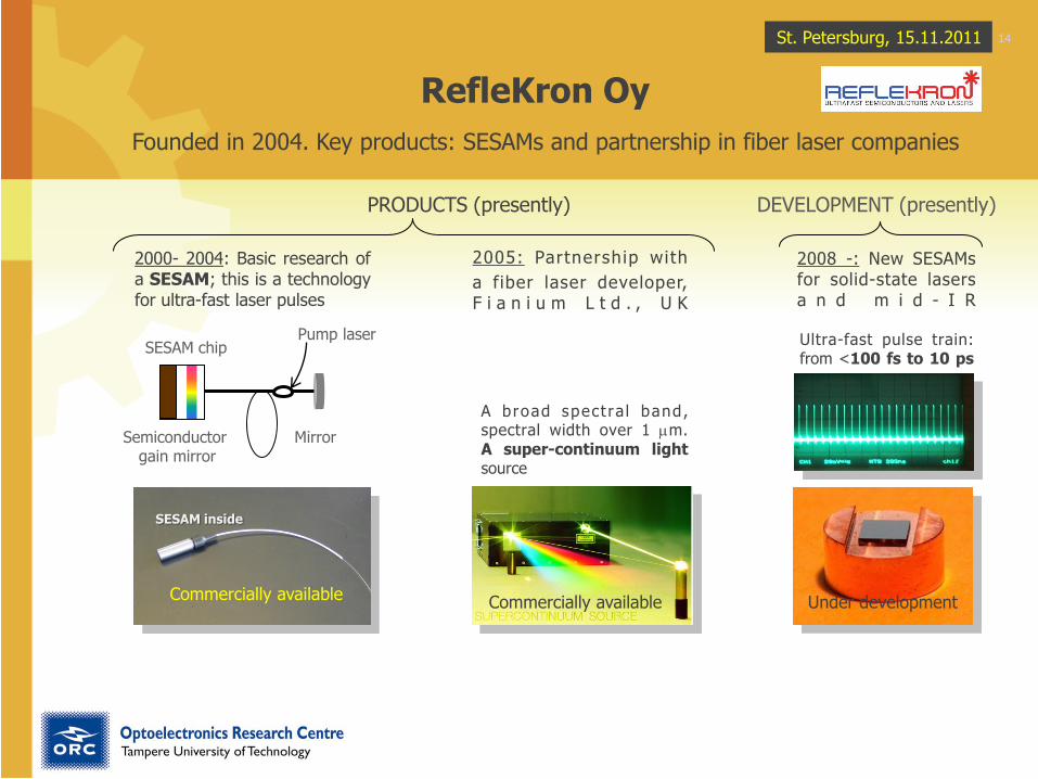
14
RefleKron Oy
Founded in 2004. Key products: SESAMs and partnership in fiber laser companies
PRODUCTS (presently) DEVELOPMENT (presently)
St. Petersburg, 15.11.2011
Semiconductor gain mirror
SESAM chip
Pump laser
Mirror
2000- 2004: Basic research of a SESAM; this is a technology for ultra-fast laser pulses
SESAM inside
Commercially available
A broad spect ra l band, spectral width over 1 m. A super-continuum light source
2005: Partnership with
a fiber laser developer, F i a n i u m L t d . , U K
Commercially available
2008 -: New SESAMs for solid-state lasers a n d m i d - I R
Ultra-fast pulse train: from <100 fs to 10 ps
Under development

15
22.2.2010
New potential business
St. Petersburg, 15.11.2011
• Optically pumped surface-emitting lasers • Surface gratings for DFB semiconductor lasers • GaAs-based multi-junction solar cells

16
Optically pumped disk laser operating at > 1 m
Output beam
Heat spreader (diamond)
Substrate
Multi-QW’s & bottom Bragg-mirror
Heat sink (Cu)
Vertical external cavity surface emitting laser, VECSEL
Lens
Heat dissipation
St. Petersburg, 15.11.2011

590 6000,0
0,5
1,0
0 10 20 30 40 500
2
4
6
8
10
12
Ou
tput
Po
we
r (W
)
Absorbed Pump Power (W)
Inte
nsity (
a.u
.)
(nm)
17
Optically pumped disk laser at yellow wavelength by frequency doubling. One application: ELT
Image c
ourt
esy o
f E
SO
/ S
tefa
n S
eip
Work on a yellow laser at 589 nm by frequency doubling is under way in Finland together with two US companies to create an artificial (sodium) star for Extremely Large Telescope (ELT)
St. Petersburg, 15.11.2011
Primary output at 1180 nm

Long-term basic research in high technology may lead to new products
Photonics and Modern Imaging Techniques
18
22.2.2010
7-W at the yellow wavelength, 589 nm (at sodium-atom resonance)
St. Petersburg, 15.11.2011

19
22.2.2010
New potential applications for business
• Optically pumped surface-emitting lasers • Surface gratings for DFB semiconductor lasers •GaAs-based multi-junction solar cells

Application of nano-imprint lithography:
1.55 µm DFB laser for high-speed telecomm
20
Edge-emitting laser diodes with NIL-based surface gratings
for high modulation bandwidth, 40 GHz (theoretical), at the photon - photon
resonance; experimentally we have got a carrier – photon peak at 20 GHz, 2011
1530 1535 1540 1545 1550 1555 1560
-70
-60
-50
-40
-30
-20
-10
0
100mA CW
200mA CW
300mA CW
Po
we
r (d
Bm
)
Wavelength (nm)
BID43398
As Cleaved
600 µm cavity
20 oC
SMSR 60 dB
0 5 10 15 20 25 30 35 40
-20
-10
0
10
20
30
40
Photon-photon
resonance
Carrier-photon
resonance
Mo
du
lati
on
re
sp
on
se
(d
B)
Frequency (GHz)
The emission peak is well locked !
An European development project:
St. Petersburg, 15.11.2011
+

22.2.2010
New potential applications for business
• Optically pumped surface-emitting lasers • Surface gratings for DFB semiconductor lasers • GaAs-based multi-junction solar cells

Another dilute nitride application :
Solar cells for concentrated photo-voltaics
22
40 % - 1 sun
52 % - 500 suns 38% - 1 sun
47 % - 500 suns
THEORY:
Theoretically, it is possible to obtain a 70-% efficiency with very many junctions. The highest efficiency obtained experimentally in US is 41.1 % for a 4-junction-cell under 1000 -sun illumination
for sunlight focusing on the solar cell
St. Petersburg, 15.11.2011

23
MBE-grown dilute nitride (InGaNAs) 3J-solar cells. Results under 1-sun light (in open air)
0,0 0,5 1,0 1,5 2,0 2,5
0
2
4
6
8
10
12
14
= 23 %
= 27.6%
Real sun (805 W/m2), GaAs current limited
= 27.6 %
Real sun (805 W/m2) + 808nm laser to generate
current of the GaAs sub-cell
1st junction GaInP E > 1.85 eV 2nd junction GaAs 1.85 > E > 1.4 eV 3rd junction GaInNAs 1.4 > E > 1 eV GaAs (100) substrate
Results obtained in August 2011
St. Petersburg, 15.11.2011
GaAs interfaces may have current-limiting sections
Our aim is to obtain >30 % in 2011 under 1-sun illumination. The present layer structure is not exactly complete

Broadband anti-reflection coatings with nano-structures
Antireflection moth-eye nano-structure at sub-wavelengths, etched on an AlInP top layer for a broad spectral-band absorption by the underneath layers, and for wide light incident angles. Back reflection: 2.5 % (theoretically 1.6 %)
400 600 800 1000 1200 1400 16000,0
0,1
0,2
0,3
0,4
0,5
0,6
0,7
0,8
0,9
1,0
Re
fle
ctivity
Wavelength (nm)
Cal624 (measured)
Cal624 (simulated)
Etch 9 (measured)
Etch 9 (simulated)
Etch ii (measured)
Etch ii (simulated)
Etch 17 (measured)
Etch 17 (simulated)
Ag mirror used as a reference
Average back-reflection at 450 - 1650 nm Because NIL is a low-cost method, this structure is suitable for use in large-area devices (e.g., solar cells)
NIL = Nano-imprint Lithography
SEM
200 nm
Published in Solar Energy Materials & Solar Cells, Vol. 94, 2010, pp. 1845-1848
St. Petersburg, 15.11.2011