Embed Size (px)
Citation preview
NJU6535
- 1 -Ver.2011-09-17
1/3 , 1/4 Duty LCD Driver GENERAL DESCRIPTION
The NJU6535 is a 1/3 or 1/4 duty LCD driver for segment type LCD panel with key scan function transmitting the 30 keys maximum scanned data (6 x 5 = 30) to CPU.
The NJU6535 chooses numbers of common, key scan, and general purpose ports by instructions. Therefore, It drives 126 segments at 1/3 duty in use of 3 commons and 42 segments or 164 segments at 1/4 duty in use of 4 and 41. Also it provides 4 general purpose output ports maximum to drive LEDs or others directly.
Furthermore, the NJU6535 can select a LCD driving voltage out of 8 steps voltage by the instruction to adjust the display contrast of LCD panel.
FEATURES
42-segment Drivers Programmable Duty Ratio 1/3 Duty : 126-segment (Maximum) 1/4 Duty : 164-segment (Maximum) 30-key Scan Function (6X5 matrix)
Needless for anti-reverse current diodes in key scan Programmable Bias Ratio 1/2, 1/3 bias Output Port for LED (maximum 4 LED) Serial Interface (SI, SO, SCL, CS) Useful Instruction set Incorporated LCD Driving Voltage Generator Circuits Electrical Variable Resistance (8-step) Logic Operating Voltage 4.5 ~ 5.5V LCD Driving Voltage ~5.5V Package Outline QFP64-H1 C-MOS Technology (Substrate :P)
PACKAGE OUTLINE
NJU6535FH1
NJU6535
- 2 - Ver.2011-09-17
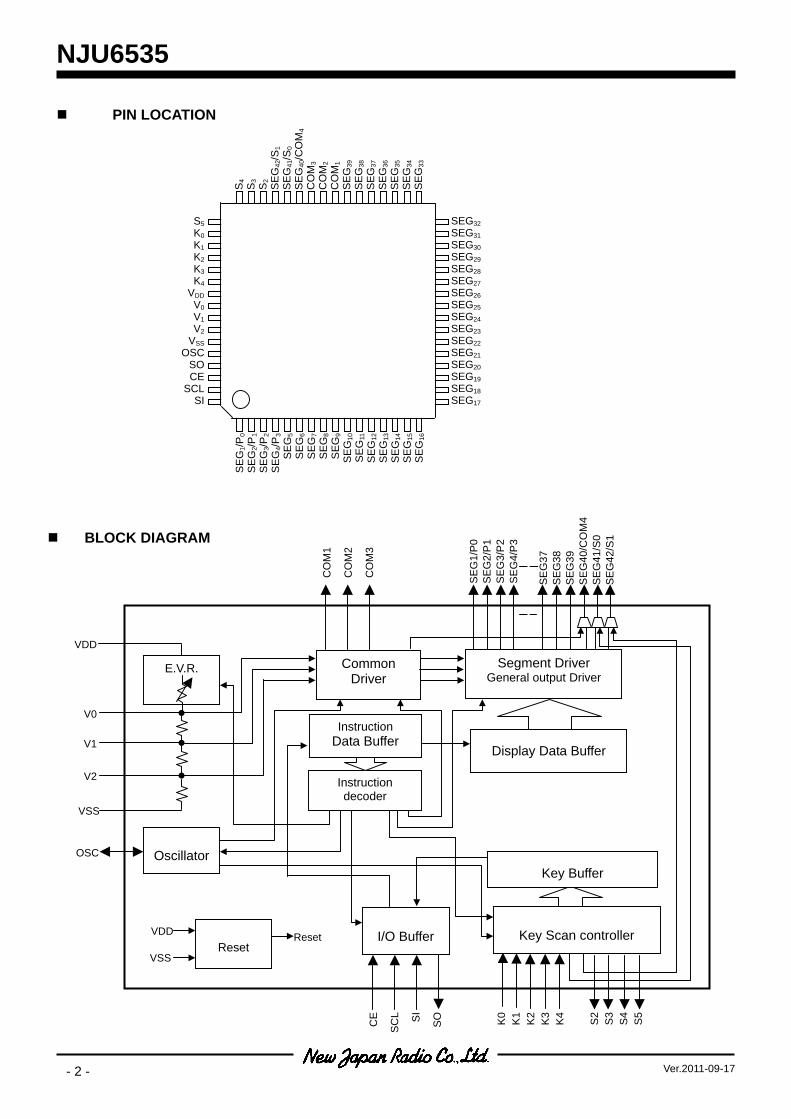
PIN LOCATION BLOCK DIAGRAM
SEG32 SEG31 SEG30 SEG29 SEG28 SEG27 SEG26 SEG25 SEG24 SEG23 SEG22 SEG21 SEG20 SEG19 SEG18 SEG17
SE
G1/P
0S
EG
2/P1
SE
G3/P
2S
EG
4/P3
SE
G5
SE
G6
SE
G7
SE
G8
SE
G9
SE
G10
SE
G11
SE
G12
SE
G13
SE
G14
SE
G15
SE
G16
S5K0K1K2K3K4
VDDV0V1V2
VSSOSC
SOCE
SCLSI
S4
S3
S2
SE
G42
/S1
SE
G41
/S0
SE
G40
/CO
M4
CO
M3
CO
M2
CO
M1
SE
G39
S
EG
38
SE
G37
S
EG
36
SE
G35
S
EG
34
SE
G33
E.V.R.
V0
V1
V2
VSS
Common Driver
Segment Driver General output Driver
CO
M1
CO
M2
CO
M3
SE
G37
S
EG
38
SE
G39
S
EG
40/C
OM
4 S
EG
41/S
0 S
EG
42/S
1
Display Data Buffer
Instruction Data Buffer
Instruction decoder
Key Buffer
Key Scan controller
S2
S3
S4
S5
I/O Buffer
K0
K1
K2
K3
K4
CE
SC
L SI
SO
Oscillator
Reset
Reset VDD
VSS
OSC
SE
G1/
P0
SE
G2/
P1
SE
G3/
P2
SE
G4/
P3
VDD
NJU6535
- 3 -Ver.2011-09-17
TERMINAL DESCRIPTION 1 No. SYMBOL I/O FUNCTION 1 2 3 4
SEG1/P0 SEG2/P1 SEG3/P2 SEG4/P3
O LCD Segment output terminal / General output terminal. Select Segment output terminal or General output terminal by the instruction.
5 to 39 SEG5 to SEG39
O LCD Segment output terminal
40 41 42
COM1 COM2 COM3
O LCD Common output terminal
43 SEG40/COM4 O LCD Segment output terminal / LCD Common output terminal SEG40 in 1/3Duty use, COM4 in 1/4Duty use.
44 45
SEG41/S0 SEG42/S1
O LCD Segment output terminals / key scanning output terminals Select Segment output terminal or key scanning output terminal by the instruction. (No need for anti-reverse current diode in key scan)
46 47 48 49
S2 to S6 O Key scanning output terminals. (No need for anti-reverse current diode in key scan)
50 to 54 K0 to K4 I Key scanning input terminals. (with internal pull-down resistor)
55 VDD - Power source: VDD=5V with LCD driving voltage input. 56 57 58
V0 V1 V2
I LCD driving voltage stabilization capacitor terminals. In use of 1/2 bias, connects V1 to V2.
59 VSS - GND: VSS=0V 60 OSC I/O System clock input terminal
This terminal should be open for internal clock operation. Change Oscillation frequency by connecting capacitor and resistor. Inputs external oscillation clock.
61 SO O Data output terminal. 62 CE I Chip enable terminal. 63 SCL I Shift clock input terminal. 64 SI I Data input terminal.
NJU6535
- 4 - Ver.2011-09-17
FUNCTIONAL DESCRIPTION (1) Description for each blocks
(1-1) Serial I/F The Serial I/F controls serial data from external data.
(1-2) Instruction Reg. The Instruction Register stores instruction code from external.
(1-3) Instruction Decoder. The instruction decoder decodes instruction code and controls each blocks
(1-4) Data Buffer for Display. The Data Buffer for Display stores data for display from external.
(1-5) Segment Driver / General output Driver. The Segment Driver generates driving waveform to Segment terminal on Display data. The General output Driver generates “H” or “L” level to General output terminal on output data.
(1-6) Common Driver. The Common Driver generates driving waveform to Common terminal .
(1-7) Electrical Variable Resistance (E.V.R.) The Electrical Variable Resistance adjusts LCD Driving Voltage from V0 to V2.
(1-8) Key Scan Controller. The Key Scan Controller controls to input from external KEY data.
(1-9) Data buffer for Key. The Data buffer for key stores Key Data until next key data is stored.
(1-10) CR Oscillator The Oscillator is CR oscillator which generates the master clock.
(1-11) Reset Circuit The Reset circuit is type of detectable voltage. It resets internal circuit when the power turns on or drop
the voltage. The Reset circuit is initializes the NJU6535 at Power ON and OFF. It generates reset signal to initialize
the system at low VDD less than power down detection voltage (2.5V typical).
NJU6535
- 5 -Ver.2011-09-17
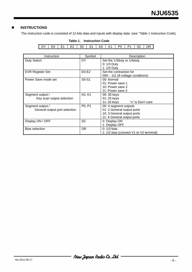
INSTRUCTIONS The instruction code is consisted of 12-bits data and inputs with display data. (see “Table 1 Instruction Code).
Table 1. Instruction Code
Instruction Symbol Description Duty Select DY Set the 1/3duty or 1/4duty.
0: 1/3 Duty 1: 1/4 Duty
EVR Register Set E0-E2 Set the contraction for 000 – 111 (8-voltage conditions)
Power Save mode set S0-S1 00: Normal 01: Power save 1 10: Power save 2 11: Power save 3
Segment output / Key scan output selection
K0, K1 00: 30 keys 01: 25 keys 1x: 20 keys “x” is Don’t care
Segment output / General output port selection
P0, P1 00: 4 segment outputs 01: 2 General output ports 10: 3 General output ports 11: 4 General output ports
Display ON / OFF SC 0: Display ON 1: Display OFF
Bias selection DR 0: 1/3 bias 1: 1/2 bias (connect V1 to V2 terminal)
DY E0 E1 E2 S0 S1 K0 K1 P0 P1 SC DR
NJU6535
- 6 - Ver.2011-09-17
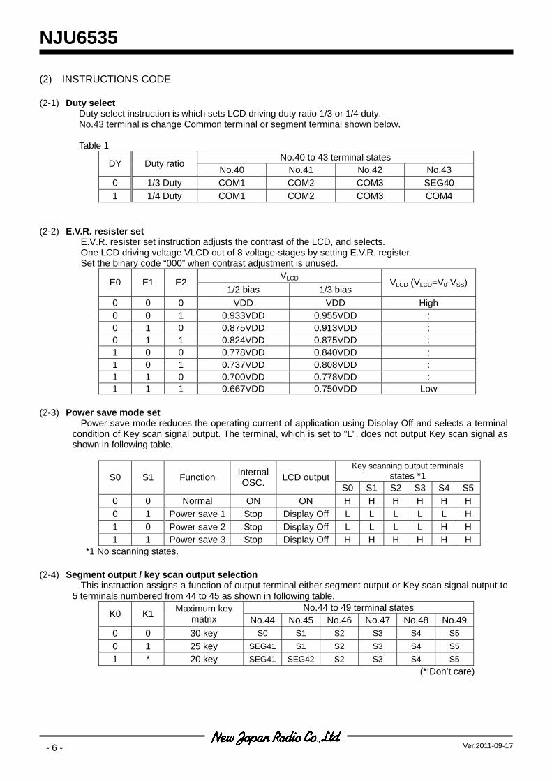
(2) INSTRUCTIONS CODE (2-1) Duty select Duty select instruction is which sets LCD driving duty ratio 1/3 or 1/4 duty. No.43 terminal is change Common terminal or segment terminal shown below.
Table 1 No.40 to 43 terminal states
DY Duty ratio No.40 No.41 No.42 No.43
0 1/3 Duty COM1 COM2 COM3 SEG40 1 1/4 Duty COM1 COM2 COM3 COM4
(2-2) E.V.R. resister set
E.V.R. resister set instruction adjusts the contrast of the LCD, and selects. One LCD driving voltage VLCD out of 8 voltage-stages by setting E.V.R. register. Set the binary code “000” when contrast adjustment is unused.
VLCD E0 E1 E2
1/2 bias 1/3 bias VLCD (VLCD=V0-VSS)
0 0 0 VDD VDD High 0 0 1 0.933VDD 0.955VDD : 0 1 0 0.875VDD 0.913VDD : 0 1 1 0.824VDD 0.875VDD : 1 0 0 0.778VDD 0.840VDD : 1 0 1 0.737VDD 0.808VDD : 1 1 0 0.700VDD 0.778VDD : 1 1 1 0.667VDD 0.750VDD Low
(2-3) Power save mode set
Power save mode reduces the operating current of application using Display Off and selects a terminal condition of Key scan signal output. The terminal, which is set to "L", does not output Key scan signal as shown in following table.
Key scanning output terminals
states *1 S0 S1 Function InternalOSC. LCD output
S0 S1 S2 S3 S4 S50 0 Normal ON ON H H H H H H 0 1 Power save 1 Stop Display Off L L L L L H 1 0 Power save 2 Stop Display Off L L L L H H 1 1 Power save 3 Stop Display Off H H H H H H
*1 No scanning states. (2-4) Segment output / key scan output selection
This instruction assigns a function of output terminal either segment output or Key scan signal output to 5 terminals numbered from 44 to 45 as shown in following table.
No.44 to 49 terminal states K0 K1 Maximum key
matrix No.44 No.45 No.46 No.47 No.48 No.490 0 30 key S0 S1 S2 S3 S4 S5 0 1 25 key SEG41 S1 S2 S3 S4 S5 1 * 20 key SEG41 SEG42 S2 S3 S4 S5
(*:Don’t care)
NJU6535
- 7 -Ver.2011-09-17
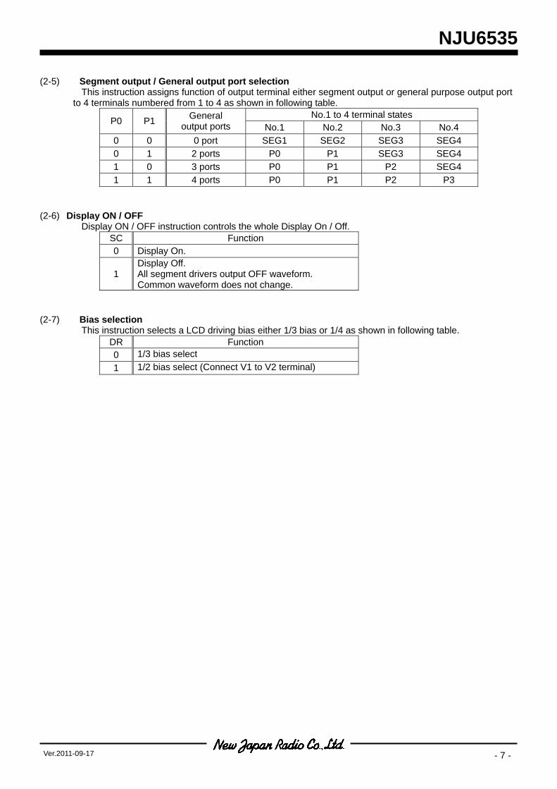
(2-5) Segment output / General output port selection This instruction assigns function of output terminal either segment output or general purpose output port
to 4 terminals numbered from 1 to 4 as shown in following table. No.1 to 4 terminal states
P0 P1 General output ports No.1 No.2 No.3 No.4
0 0 0 port SEG1 SEG2 SEG3 SEG4 0 1 2 ports P0 P1 SEG3 SEG4 1 0 3 ports P0 P1 P2 SEG4 1 1 4 ports P0 P1 P2 P3
(2-6) Display ON / OFF
Display ON / OFF instruction controls the whole Display On / Off. SC Function 0 Display On.
1 Display Off. All segment drivers output OFF waveform. Common waveform does not change.
(2-7) Bias selection
This instruction selects a LCD driving bias either 1/3 bias or 1/4 as shown in following table. DR Function 0 1/3 bias select 1 1/2 bias select (Connect V1 to V2 terminal)
NJU6535
- 8 - Ver.2011-09-17
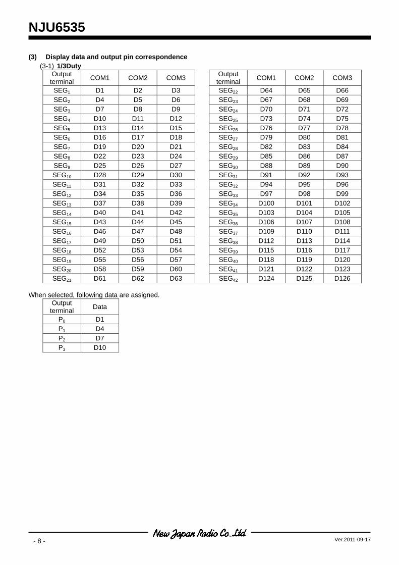
(3) Display data and output pin correspondence (3-1) 1/3Duty
Output terminal COM1 COM2 COM3 Output
terminal COM1 COM2 COM3
SEG1 D1 D2 D3 SEG22 D64 D65 D66 SEG2 D4 D5 D6 SEG23 D67 D68 D69 SEG3 D7 D8 D9 SEG24 D70 D71 D72 SEG4 D10 D11 D12 SEG25 D73 D74 D75 SEG5 D13 D14 D15 SEG26 D76 D77 D78 SEG6 D16 D17 D18 SEG27 D79 D80 D81 SEG7 D19 D20 D21 SEG28 D82 D83 D84 SEG8 D22 D23 D24 SEG29 D85 D86 D87 SEG9 D25 D26 D27 SEG30 D88 D89 D90 SEG10 D28 D29 D30 SEG31 D91 D92 D93 SEG11 D31 D32 D33 SEG32 D94 D95 D96 SEG12 D34 D35 D36 SEG33 D97 D98 D99 SEG13 D37 D38 D39 SEG34 D100 D101 D102 SEG14 D40 D41 D42 SEG35 D103 D104 D105 SEG15 D43 D44 D45 SEG36 D106 D107 D108 SEG16 D46 D47 D48 SEG37 D109 D110 D111 SEG17 D49 D50 D51 SEG38 D112 D113 D114 SEG18 D52 D53 D54 SEG39 D115 D116 D117 SEG19 D55 D56 D57 SEG40 D118 D119 D120 SEG20 D58 D59 D60 SEG41 D121 D122 D123 SEG21 D61 D62 D63
SEG42 D124 D125 D126 When selected, following data are assigned.
Output terminal Data
P0 D1 P1 D4 P2 D7 P3 D10
NJU6535
- 9 -Ver.2011-09-17
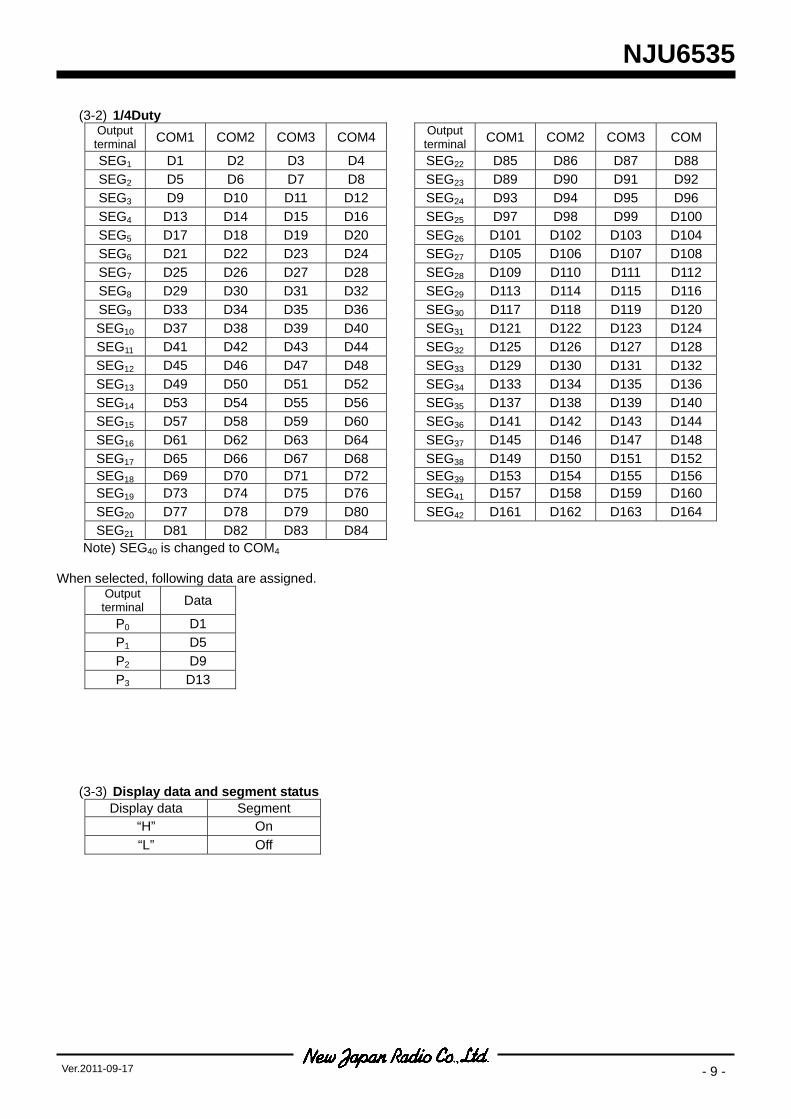
(3-2) 1/4Duty Output terminal COM1 COM2 COM3 COM4 Output
terminal COM1 COM2 COM3 COM
SEG1 D1 D2 D3 D4 SEG22 D85 D86 D87 D88 SEG2 D5 D6 D7 D8 SEG23 D89 D90 D91 D92 SEG3 D9 D10 D11 D12 SEG24 D93 D94 D95 D96 SEG4 D13 D14 D15 D16 SEG25 D97 D98 D99 D100 SEG5 D17 D18 D19 D20 SEG26 D101 D102 D103 D104 SEG6 D21 D22 D23 D24 SEG27 D105 D106 D107 D108 SEG7 D25 D26 D27 D28 SEG28 D109 D110 D111 D112 SEG8 D29 D30 D31 D32 SEG29 D113 D114 D115 D116 SEG9 D33 D34 D35 D36 SEG30 D117 D118 D119 D120 SEG10 D37 D38 D39 D40 SEG31 D121 D122 D123 D124 SEG11 D41 D42 D43 D44 SEG32 D125 D126 D127 D128 SEG12 D45 D46 D47 D48 SEG33 D129 D130 D131 D132 SEG13 D49 D50 D51 D52 SEG34 D133 D134 D135 D136 SEG14 D53 D54 D55 D56 SEG35 D137 D138 D139 D140 SEG15 D57 D58 D59 D60 SEG36 D141 D142 D143 D144 SEG16 D61 D62 D63 D64 SEG37 D145 D146 D147 D148 SEG17 D65 D66 D67 D68 SEG38 D149 D150 D151 D152 SEG18 D69 D70 D71 D72 SEG39 D153 D154 D155 D156 SEG19 D73 D74 D75 D76 SEG41 D157 D158 D159 D160 SEG20 D77 D78 D79 D80
SEG42 D161 D162 D163 D164 SEG21 D81 D82 D83 D84
Note) SEG40 is changed to COM4 When selected, following data are assigned.
Output terminal Data
P0 D1 P1 D5 P2 D9 P3 D13
(3-3) Display data and segment status Display data Segment
“H” On “L” Off
NJU6535
- 10 - Ver.2011-09-17
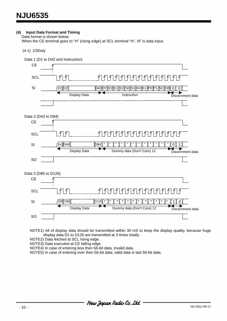
(4) Input Data Format and Timing Data format is shown below. When the CE terminal goes to “H” (rising edge) at SCL terminal “H”, I/F is data input. (4-1) 1/3Duty Data 1 (D1 to D42 and Instruction) Data 2 (D43 to D84) Data 3 (D85 to D126)
NOTE1) All of display data should be transmitted within 30 mS to keep the display quality, because huge display data D1 to D126 are transmitted at 3 times totally.
NOTE2) Data fetched at SCL rising edge. NOTE3) Data executed at CE falling edge. NOTE4) In case of entering less then 56-bit data, invalid data. NOTE5) In case of entering over then 56-bit data, valid data is last 56-bit data.
CE
SI
Discernment dataDisplay Data Instruction
D1 D2 D42 DY E0 E1 E2 S0 S1 K0 K1 P0 P1 SC DR 0 0
SCL
CE
SCL
SI
SO
D43D44 D84 * * * * * * * * * * * * 0 1
Discernment data Display Data Dummy data (Don’t Care) 12
D85 D86 D126 * * * * * * * * * * * * 1 0
Discernment data Display Data Dummy data (Don’t Care) 12
CE
SCL
SI
SO
NJU6535
- 11 -Ver.2011-09-17
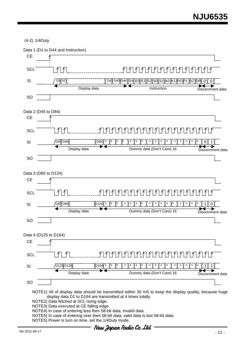
(4-2) 1/4Duty
Data 1 (D1 to D44 and Instruction)
Data 2 (D45 to D84)
Data 3 (D85 to D124)
Data 4 (D125 to D164)
NOTE1) All of display data should be transmitted within 30 mS to keep the display quality, because huge display data D1 to D164 are transmitted at 4 times totally.
NOTE2) Data fetched at SCL rising edge. NOTE3) Data executed at CE falling edge. NOTE4) In case of entering less then 58-bit data, invalid data. NOTE5) In case of entering over then 58-bit data, valid data is last 58-bit data. NOTE5) Power is turn on time, set the 1/4Duty mode.
CE
SCL
SI
SO
Discernment data Display data Instruction
D1 D2 D42 D43 D44 DY E0 E1 E2 S0 S1 K0 K1 P0 P1 SC DR 0 0
CE
SCL
SI
SO
D45 D46 D84 * * * * * * * * * * * * * * * * 0 1
Discernment data Display data Dummy data (Don’t Care) 16
CE
SCL
SI
SO
D85 D86 D124 * * * * * * * * * * * * * * * * 1 0
Discernment data Display data Dummy data (Don’t Care) 16
CE
SCL
SI
SO
D125 D126 D164 * * * * * * * * * * * * * * * * 1 1
Discernment data Display data Dummy data (Don’t Care) 16
NJU6535
- 12 - Ver.2011-09-17
(5) Power save mode Power save mode 1 to 3 is set by “1” level as a control data in PS0 or 1, and released by “0” in PS0 and PS1.
In power save mode, segment drivers and commons output “L” level and the internal oscillation circuit is stop the operation ( but operates at Key in detection) for operation current reduction.
However, output terminals SEG1/P0 to SEG4/P3 operate as General output port set by control data P0 and P1 in power save mode. (refer (1)Instruction (e)Segment output / General output port)
(6) Key scan circuit
Key scan circuit connects the 6 x 5 key-matrix maximum and reads the data of 30 keys maximum. It chooses the number of keys in key-matrix by “Segment output / key scan output select” instruction. It outputs a identified key data to CPU after comparison with two data read from the key-matrix in twice for reliable key operation. If those data are not identified, key data is not outputted. It outputs “L” signal through “SO” terminal as the request after 577T[s] (T=1/fosc) when any key is operated. Furthermore, the key scan circuit structures for reducing the external components like as Diodes to prevent circuit short problem.
(6-1) The relation between output data and key matrix The relation between output data and key matrix shows bellow table and sets “1” signal for operated key. In case of 20 keys application, unassigned area for keys from KD1 to KD10 in bellow table take “0” signal. In
case of 25 keys application, unassigned area from KD1 to KD5 take “0” signal also. In mode of Power save 1, area for keys from KD1 to KD25 in bellow table take “0” signal. In mode of Power
save 2, area from KD1 to KD20 take “0” signal also. The terminals, which are not connected any keys, should be open. K0 K1 K2 K3 K4
S0 KD1 KD2 KD3 KD4 KD5 S1 KD6 KD7 KD8 KD9 KD10 S2 KD11 KD12 KD13 KD14 KD15 S3 KD16 KD17 KD18 KD19 KD20 S4 KD21 KD22 KD23 KD24 KD25 S5 KD26 KD27 KD28 KD29 KD30
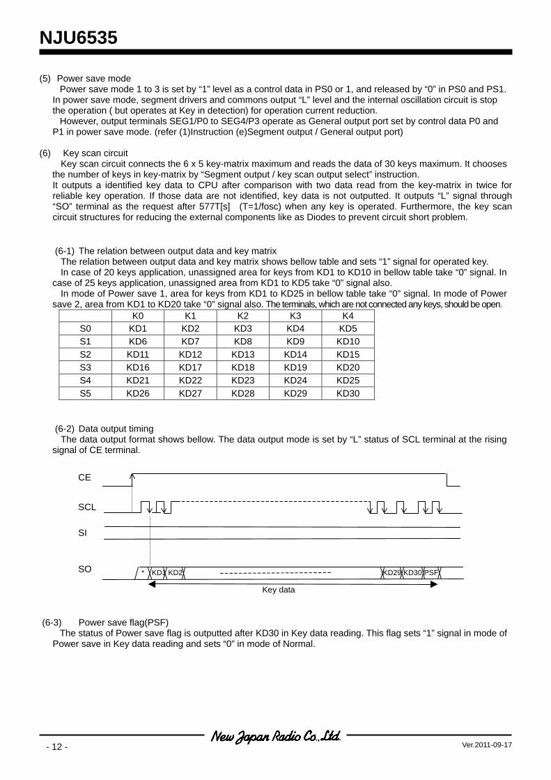
(6-2) Data output timing The data output format shows bellow. The data output mode is set by “L” status of SCL terminal at the rising
signal of CE terminal. (6-3) Power save flag(PSF)
The status of Power save flag is outputted after KD30 in Key data reading. This flag sets “1” signal in mode of Power save in Key data reading and sets “0” in mode of Normal.
* KD1 KD2 KD29 KD30 PSF
Key data
CE
SCL
SI
SO
NJU6535
- 13 -Ver.2011-09-17
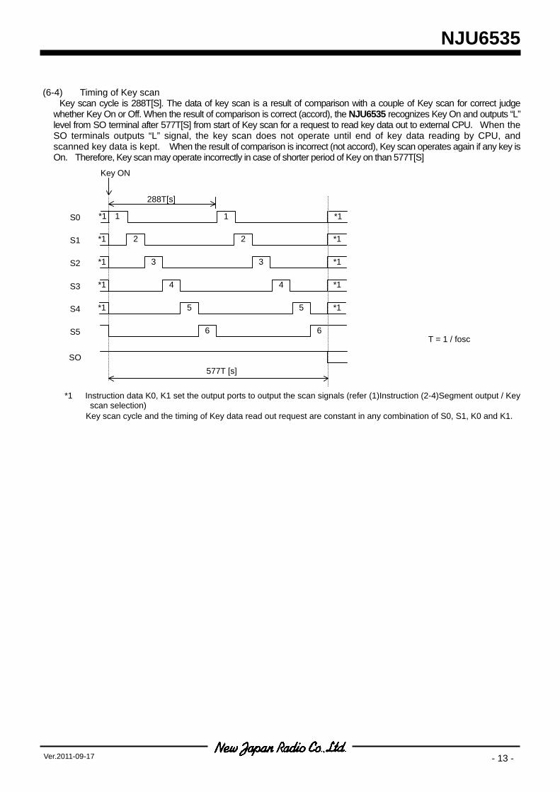
(6-4) Timing of Key scan
Key scan cycle is 288T[S]. The data of key scan is a result of comparison with a couple of Key scan for correct judge whether Key On or Off. When the result of comparison is correct (accord), the NJU6535 recognizes Key On and outputs “L” level from SO terminal after 577T[S] from start of Key scan for a request to read key data out to external CPU. When the SO terminals outputs “L” signal, the key scan does not operate until end of key data reading by CPU, and scanned key data is kept. When the result of comparison is incorrect (not accord), Key scan operates again if any key is On. Therefore, Key scan may operate incorrectly in case of shorter period of Key on than 577T[S]
*1 Instruction data K0, K1 set the output ports to output the scan signals (refer (1)Instruction (2-4)Segment output / Key scan selection)
Key scan cycle and the timing of Key data read out request are constant in any combination of S0, S1, K0 and K1.
T = 1 / fosc
S0
S1
S2
S3
S5
S4
SO
6 6
1 *1
2 2*1 *1
3 3*1 *1
4 4*1 *1
5 5*1 *1
577T [s]
288T[s]
Key ON
*1 1
NJU6535
- 14 - Ver.2011-09-17
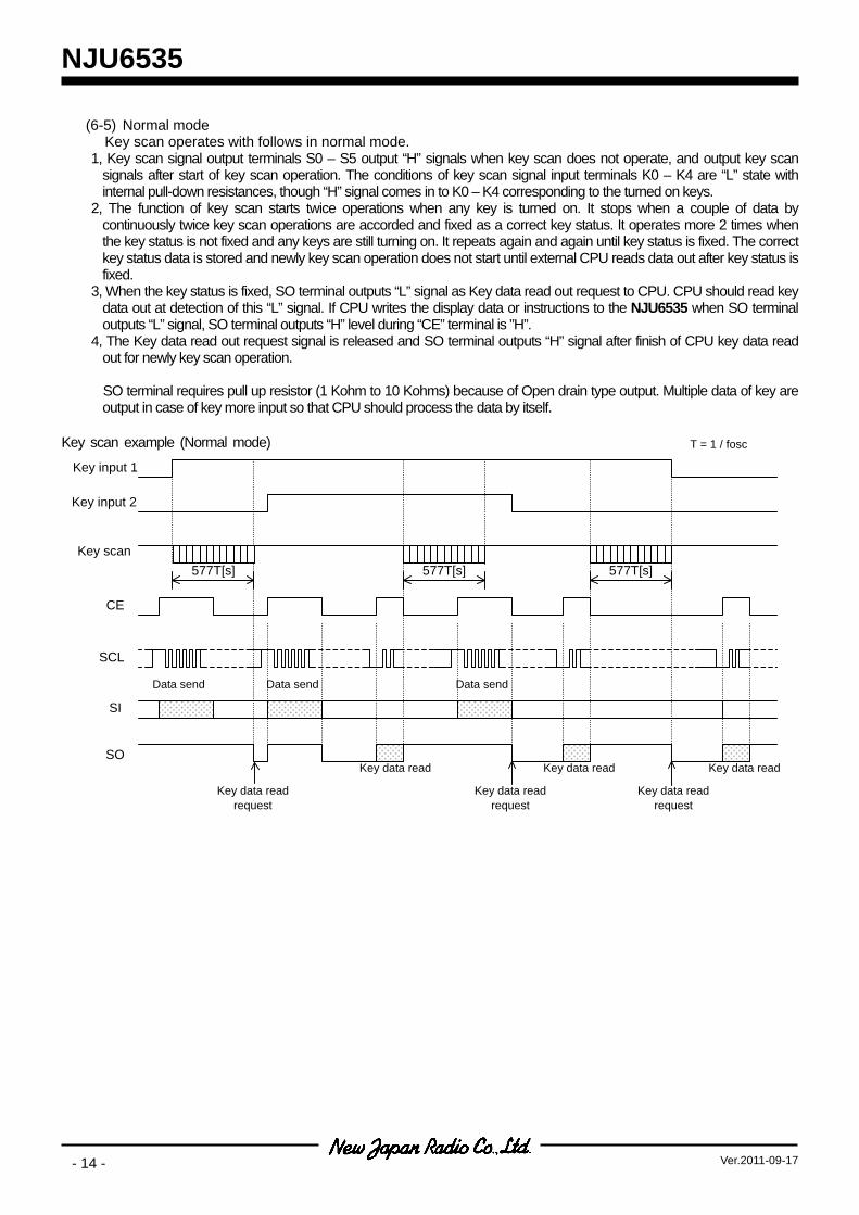
(6-5) Normal mode Key scan operates with follows in normal mode.
1, Key scan signal output terminals S0 – S5 output “H” signals when key scan does not operate, and output key scan signals after start of key scan operation. The conditions of key scan signal input terminals K0 – K4 are “L” state with internal pull-down resistances, though “H” signal comes in to K0 – K4 corresponding to the turned on keys.
2, The function of key scan starts twice operations when any key is turned on. It stops when a couple of data by continuously twice key scan operations are accorded and fixed as a correct key status. It operates more 2 times when the key status is not fixed and any keys are still turning on. It repeats again and again until key status is fixed. The correct key status data is stored and newly key scan operation does not start until external CPU reads data out after key status is fixed.
3, When the key status is fixed, SO terminal outputs “L” signal as Key data read out request to CPU. CPU should read key data out at detection of this “L” signal. If CPU writes the display data or instructions to the NJU6535 when SO terminal outputs “L” signal, SO terminal outputs “H” level during “CE” terminal is ”H”.
4, The Key data read out request signal is released and SO terminal outputs “H” signal after finish of CPU key data read out for newly key scan operation.
SO terminal requires pull up resistor (1 Kohm to 10 Kohms) because of Open drain type output. Multiple data of key are
output in case of key more input so that CPU should process the data by itself.
Key scan example (Normal mode)
SO
Key data read request
Key data read
Key data readrequest
Key data read Key data read
T = 1 / fosc
CE
Key input 1
Key input 2
Data send
SI
Key scan 577T[s] 577T[s] 577T[s]
SCL
Data send Data send
Key data read request
NJU6535
- 15 -Ver.2011-09-17
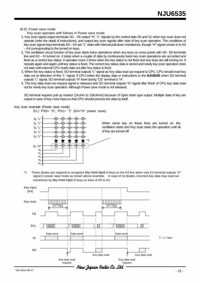
(6-6) Power save mode Key scan operates with follows in Power save mode.
1, Key scan signal output terminals S0 – S5 output “H”, “L” signals by the control data S0 and S1 when key scan does not operate (refer the detail of instructions), and output key scan signals after start of key scan operation. The conditions of key scan signal input terminals K0 – K4 are “L” state with internal pull-down resistances, though “H” signal comes in to K0 – K4 corresponding to the turned on keys.
2, The oscillation circuit function of key scan starts twice operations when any keys on cross points with S0– S5 terminals line and K0 – Ki turned on. It stops when a couple of data by continuously twice key scan operations are accorded and fixed as a correct key status. It operates more 2 times when the key status is not fixed and any keys are still turning on. It repeats again and again until key status is fixed. The correct key status data is stored and newly key scan operation does not start until external CPU reads data out after key status is fixed.
3, When the key status is fixed, SO terminal outputs “L” signal as Key data read out request to CPU. CPU should read key data out at detection of this “L” signal. If CPU writes the display data or instructions to the NJU6535 when SO terminal outputs “L” signal, SO terminal outputs “H” level during “CE” terminal is ”H”.
4, The Key data read out request signal is released and SO terminal outputs “H” signal after finish of CPU key data read out for newly key scan operation. Although Power save mode is not released.
SO terminal requires pull up resistor (1Kohm to 10Kohms) because of Open drain type output. Multiple data of key are
output in case of key more input so that CPU should process the data by itself.
Key scan example (Power save mode) Ex.) PS0= ”0”, PS1= ”1” (K4=“H” power save)
*1 These diodes are required to recognize key more input of keys on the K4 line when only K4 terminal outputs “H” signal in power save mode as shown above example. In case of no diodes, incorrect key data may read out sometimes by key more input of keys on lines of K0 to K4.
Data send Data send Data sendSI
Key input (K4)
Key scan 577T[s] 577T[s]
CE
SCL
SO
Key data read request
Key data read
Key data readrequest
Key data read
T = 1 / fosc
When some key on these lines are turned on, the oscillation starts and Key scan starts the operation until all of key are turned off.
*1
S0 “L”S1 “L”S2 “L”S3 “L”S4 “L”
S5 “H”K0K1K2K3K4
NJU6535
- 16 - Ver.2011-09-17
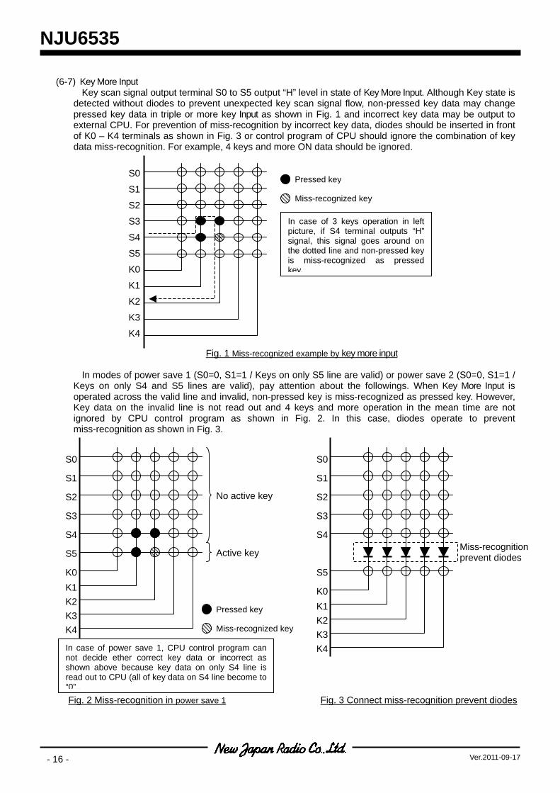
(6-7) Key More Input Key scan signal output terminal S0 to S5 output “H” level in state of Key More Input. Although Key state is
detected without diodes to prevent unexpected key scan signal flow, non-pressed key data may change pressed key data in triple or more key Input as shown in Fig. 1 and incorrect key data may be output to external CPU. For prevention of miss-recognition by incorrect key data, diodes should be inserted in front of K0 – K4 terminals as shown in Fig. 3 or control program of CPU should ignore the combination of key data miss-recognition. For example, 4 keys and more ON data should be ignored.
Fig. 1 Miss-recognized example by key more input
In modes of power save 1 (S0=0, S1=1 / Keys on only S5 line are valid) or power save 2 (S0=0, S1=1 /
Keys on only S4 and S5 lines are valid), pay attention about the followings. When Key More Input is operated across the valid line and invalid, non-pressed key is miss-recognized as pressed key. However, Key data on the invalid line is not read out and 4 keys and more operation in the mean time are not ignored by CPU control program as shown in Fig. 2. In this case, diodes operate to prevent miss-recognition as shown in Fig. 3.
Fig. 2 Miss-recognition in power save 1 Fig. 3 Connect miss-recognition prevent diodes
S0
S1
S2
S3
S4
S5
K0
K1
K2
K3
K4
Pressed key
Miss-recognized key
In case of 3 keys operation in leftpicture, if S4 terminal outputs “H”signal, this signal goes around onthe dotted line and non-pressed keyis miss-recognized as pressedkey.
In case of power save 1, CPU control program cannot decide ether correct key data or incorrect asshown above because key data on only S4 line isread out to CPU (all of key data on S4 line become to“0”..
S0
S1
S2
S3
S4
S5
K0 K1 K2 K3 K4
Pressed key
Miss-recognized key
No active key
Active key
S0
S1
S2
S3
S4
S5
K0K1K2K3K4
Miss-recognition prevent diodes
NJU6535
- 17 -Ver.2011-09-17
(6-8) Key data reading out operation by external CPU
(a) Display data writing
Display data and instruction change operate at the rising edge of signal into CE terminal. Written data or instructions do not operate during CE terminal “H”. When the time to write whole display data into Data Buffer becomes too long by huge display data, display may be effected unexpected display. Data writing order from Data 1 to Data 3 in 1/3 duty or Data 1 to Data 4 in 1/4 duty is not limited.
The duty is 1/3 after initialization. For 1/4 duty operation, Data 1 must be written first after initialization
(b) Key data reading out operation
The minimum period from Key in to SO terminal = “L” is 577T(t1) by key scan operation. When key scan operation performs again for key data fix preventing from noise or bouncing of key, the period from Key in to SO terminal = “L” is 1200T(t1). When the SO terminal outputs “L”, the key scan operation is stopped after execution of key data reading out operation. Therefore, fixed key data is kept until end of key data reading out operation. When key data reading out operation is performed during SO terminal = “H”, both of key data from KD1 to KD30 and power save flag (PSF) are not outputted correctly.
Key data reading out operation example
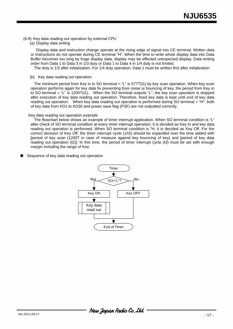
The flowchart below shows an example of timer interrupt application. When SO terminal condition is “L” after check of SO terminal condition at every timer interrupt operation, it is decided as Key In and key data reading out operation is performed. When SO terminal condition is “H, it is decided as Key Off. For the correct decision of Key Off, the timer interrupt cycle (1/t3) should be expanded over the time added with [period of key scan (1200T in case of measure against key bouncing of key) and [period of key data reading out operation (t2)]. In this time, the period of timer interrupt cycle (t3) must be set with enough margin including the range of fosc.
Sequence of key data reading out operation
Timer
SO=”L”?
Key OFF Key ON
Key data read out
End of Timer
Yes No
NJU6535
- 18 - Ver.2011-09-17
Timing chart of key data reading out operation
t1: Key scan time t2: Key data read time t3: Interrupt cycle
*: t3 > t1 + t2
Key input
SO
CE
Decision
Interrupt
SCL
Key ON
t1 t2 t2t1
Key ON Key OFF Key OFF
t3 t3 t3
Key OFF
t3
t1
NJU6535
- 19 -Ver.2011-09-17
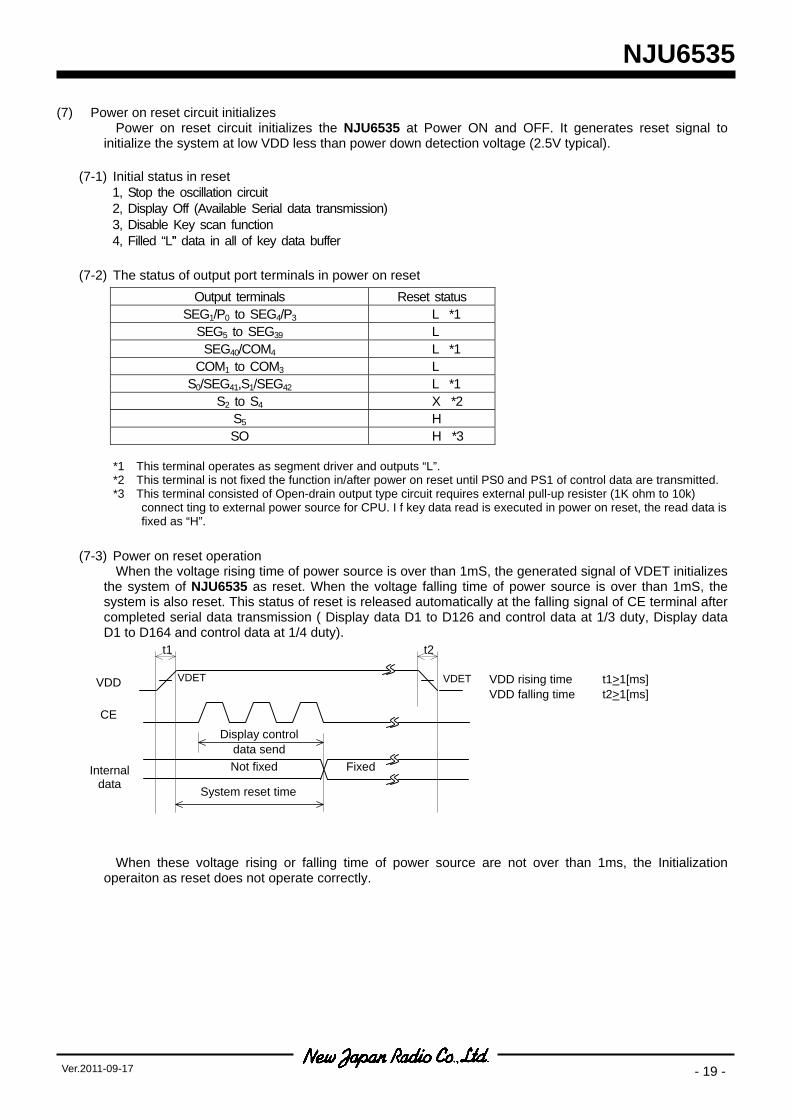
(7) Power on reset circuit initializes Power on reset circuit initializes the NJU6535 at Power ON and OFF. It generates reset signal to
initialize the system at low VDD less than power down detection voltage (2.5V typical).
(7-1) Initial status in reset 1, Stop the oscillation circuit 2, Display Off (Available Serial data transmission) 3, Disable Key scan function 4, Filled “L”” data in all of key data buffer
(7-2) The status of output port terminals in power on reset
*1 This terminal operates as segment driver and outputs “L”. *2 This terminal is not fixed the function in/after power on reset until PS0 and PS1 of control data are transmitted. *3 This terminal consisted of Open-drain output type circuit requires external pull-up resister (1K ohm to 10k)
connect ting to external power source for CPU. I f key data read is executed in power on reset, the read data is fixed as “H”.
(7-3) Power on reset operation
When the voltage rising time of power source is over than 1mS, the generated signal of VDET initializes the system of NJU6535 as reset. When the voltage falling time of power source is over than 1mS, the system is also reset. This status of reset is released automatically at the falling signal of CE terminal after completed serial data transmission ( Display data D1 to D126 and control data at 1/3 duty, Display data D1 to D164 and control data at 1/4 duty).
When these voltage rising or falling time of power source are not over than 1ms, the Initialization operaiton as reset does not operate correctly.
Output terminals Reset status SEG1/P0 to SEG4/P3 L *1
SEG5 to SEG39 L SEG40/COM4 L *1
COM1 to COM3 L S0/SEG41,S1/SEG42 L *1
S2 to S4 X *2 S5 H SO H *3
VDD rising time t1>1[ms] VDD falling time t2>1[ms]
Display control data send
VDET
t2
VDET
t1
System reset time
Not fixed Fixed
VDD
CE
Internal data
NJU6535
- 20 - Ver.2011-09-17
(8) LCD panel drive
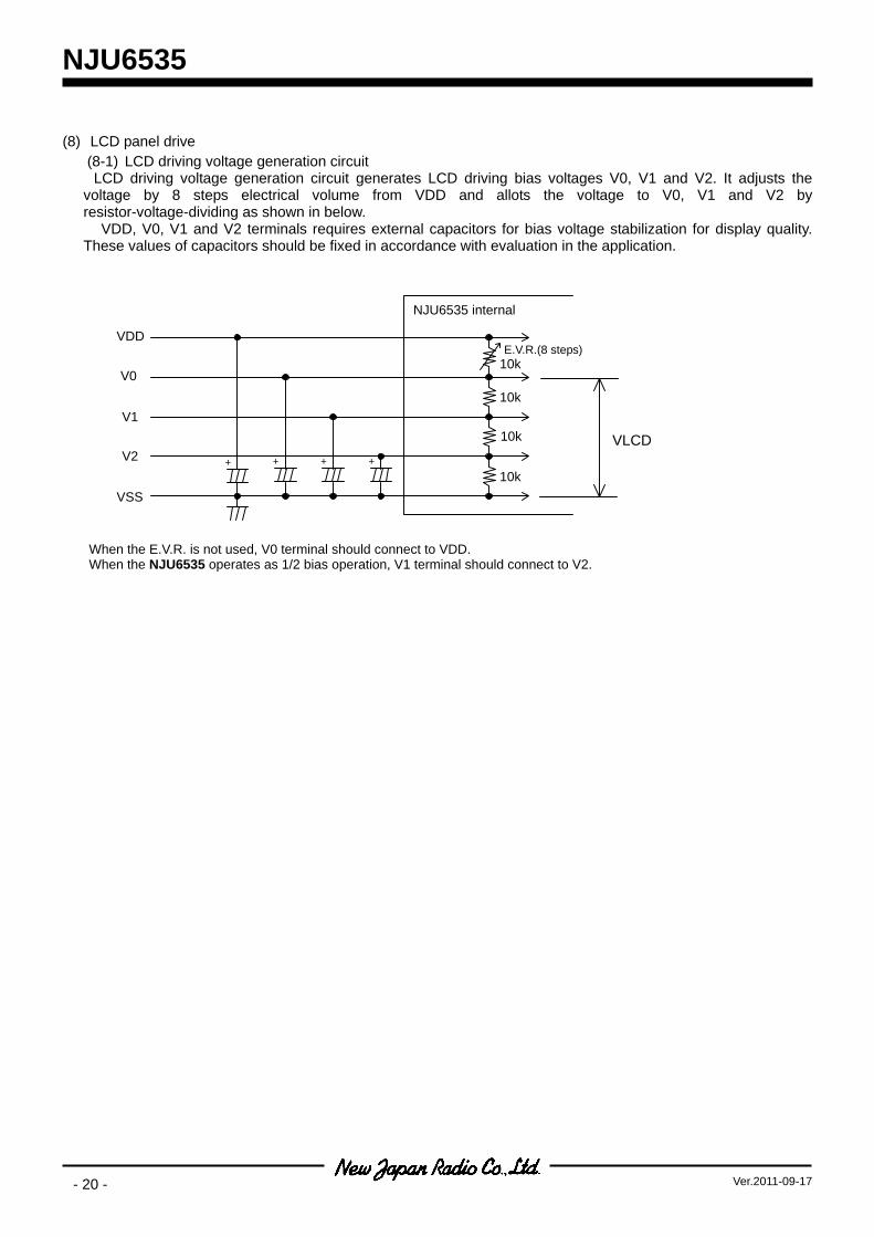
(8-1) LCD driving voltage generation circuit LCD driving voltage generation circuit generates LCD driving bias voltages V0, V1 and V2. It adjusts the
voltage by 8 steps electrical volume from VDD and allots the voltage to V0, V1 and V2 by resistor-voltage-dividing as shown in below.
VDD, V0, V1 and V2 terminals requires external capacitors for bias voltage stabilization for display quality. These values of capacitors should be fixed in accordance with evaluation in the application.
When the E.V.R. is not used, V0 terminal should connect to VDD. When the NJU6535 operates as 1/2 bias operation, V1 terminal should connect to V2.
++ + +
VDD
V0
V1
V2
VSS
NJU6535 internal
10k
10k
10k
10k
E.V.R.(8 steps)
VLCD
NJU6535
- 21 -Ver.2011-09-17
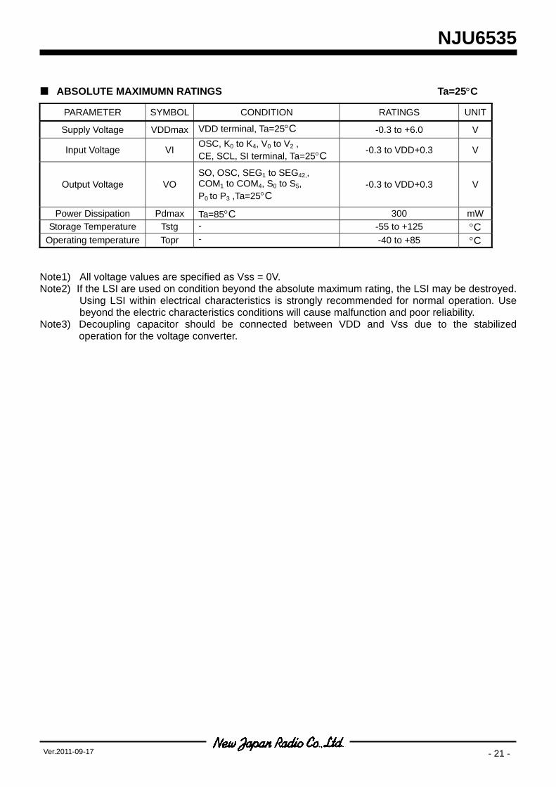
ABSOLUTE MAXIMUMN RATINGS Ta=25°C
PARAMETER SYMBOL CONDITION RATINGS UNIT
Supply Voltage VDDmax VDD terminal, Ta=25°C -0.3 to +6.0 V
Input Voltage VI OSC, K0 to K4, V0 to V2 , CE, SCL, SI terminal, Ta=25°C -0.3 to VDD+0.3 V
Output Voltage VO SO, OSC, SEG1 to SEG42,, COM1 to COM4, S0 to S5, P0 to P3 ,Ta=25°C
-0.3 to VDD+0.3 V
Power Dissipation Pdmax Ta=85°C 300 mWStorage Temperature Tstg - -55 to +125 °C
Operating temperature Topr - -40 to +85 °C Note1) All voltage values are specified as Vss = 0V. Note2) If the LSI are used on condition beyond the absolute maximum rating, the LSI may be destroyed.
Using LSI within electrical characteristics is strongly recommended for normal operation. Use beyond the electric characteristics conditions will cause malfunction and poor reliability.
Note3) Decoupling capacitor should be connected between VDD and Vss due to the stabilized operation for the voltage converter.
NJU6535
- 22 - Ver.2011-09-17
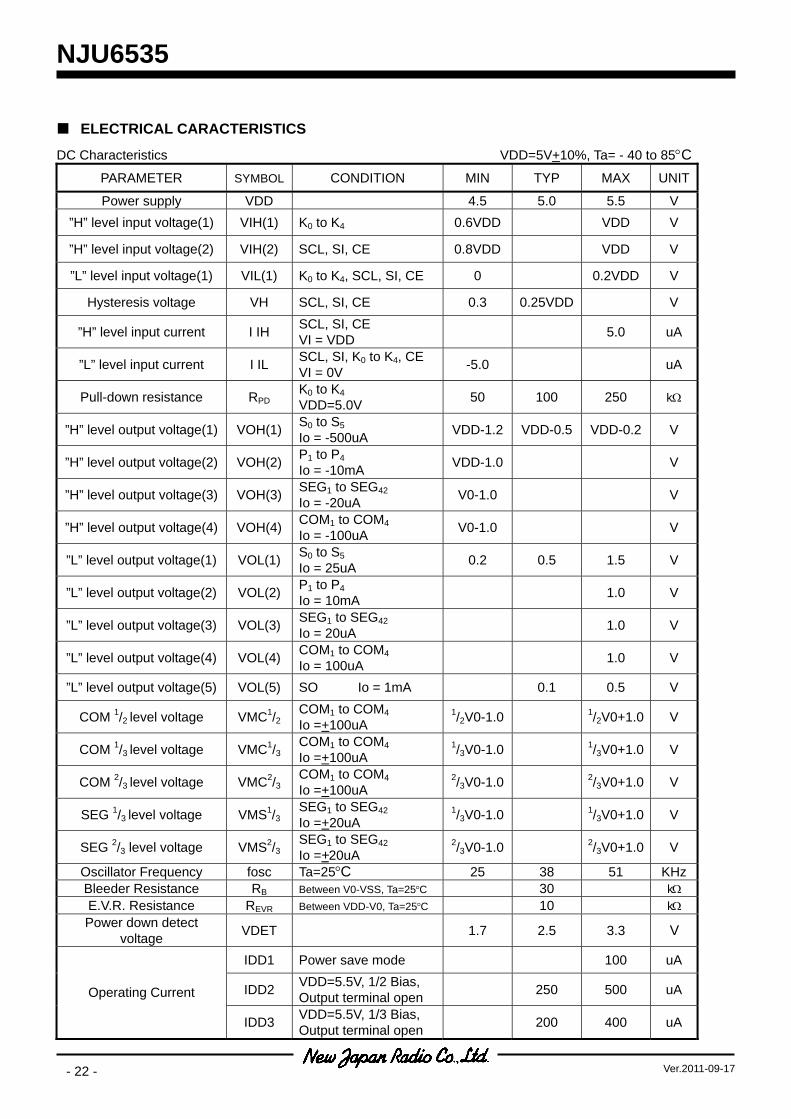
ELECTRICAL CARACTERISTICS
DC Characteristics VDD=5V+10%, Ta= - 40 to 85°C
PARAMETER SYMBOL CONDITION MIN TYP MAX UNIT
Power supply VDD 4.5 5.0 5.5 V ”H” level input voltage(1) VIH(1) K0 to K4 0.6VDD VDD V
”H” level input voltage(2) VIH(2) SCL, SI, CE 0.8VDD VDD V
”L” level input voltage(1) VIL(1) K0 to K4, SCL, SI, CE 0 0.2VDD V
Hysteresis voltage VH SCL, SI, CE 0.3 0.25VDD V
”H” level input current I IH SCL, SI, CE VI = VDD 5.0 uA
”L” level input current I IL SCL, SI, K0 to K4, CE VI = 0V -5.0 uA
Pull-down resistance RPD K0 to K4 VDD=5.0V 50 100 250 kΩ
”H” level output voltage(1) VOH(1) S0 to S5 Io = -500uA VDD-1.2 VDD-0.5 VDD-0.2 V
”H” level output voltage(2) VOH(2) P1 to P4 Io = -10mA VDD-1.0 V
”H” level output voltage(3) VOH(3) SEG1 to SEG42 Io = -20uA V0-1.0 V
”H” level output voltage(4) VOH(4) COM1 to COM4 Io = -100uA V0-1.0 V
”L” level output voltage(1) VOL(1) S0 to S5 Io = 25uA 0.2 0.5 1.5 V
”L” level output voltage(2) VOL(2) P1 to P4 Io = 10mA 1.0 V
”L” level output voltage(3) VOL(3) SEG1 to SEG42 Io = 20uA 1.0 V
”L” level output voltage(4) VOL(4) COM1 to COM4 Io = 100uA 1.0 V
”L” level output voltage(5) VOL(5) SO Io = 1mA 0.1 0.5 V
COM 1/2 level voltage VMC1/2 COM1 to COM4 Io =+100uA
1/2V0-1.0 1/2V0+1.0 V
COM 1/3 level voltage VMC1/3 COM1 to COM4 Io =+100uA
1/3V0-1.0 1/3V0+1.0 V
COM 2/3 level voltage VMC2/3 COM1 to COM4 Io =+100uA
2/3V0-1.0 2/3V0+1.0 V
SEG 1/3 level voltage VMS1/3 SEG1 to SEG42 Io =+20uA
1/3V0-1.0 1/3V0+1.0 V
SEG 2/3 level voltage VMS2/3 SEG1 to SEG42 Io =+20uA
2/3V0-1.0 2/3V0+1.0 V
Oscillator Frequency fosc Ta=25°C 25 38 51 KHzBleeder Resistance RB Between V0-VSS, Ta=25°C 30 kΩ E.V.R. Resistance REVR Between VDD-V0, Ta=25°C 10 kΩ Power down detect
voltage VDET 1.7 2.5 3.3 V
IDD1 Power save mode 100 uA
IDD2 VDD=5.5V, 1/2 Bias, Output terminal open 250 500 uA Operating Current
IDD3 VDD=5.5V, 1/3 Bias, Output terminal open 200 400 uA
NJU6535
- 23 -Ver.2011-09-17
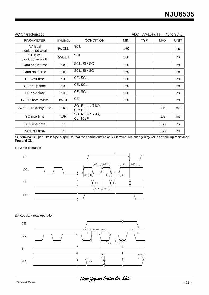
AC Characteristics VDD=5V+10%, Ta= - 40 to 85°C
PARAMETER SYMBOL CONDITION MIN TYP MAX UNIT
“L” level clock pulse width tWCLL SCL 160 ns
“H” level clock pulse width tWCLH SCL 160 ns
Data setup time tDS SCL, SI / SO 160 ns
Data hold time tDH SCL, SI / SO 160 ns
CE wait time tCP CE, SCL 160 ns
CE setup time tCS CE, SCL 160 ns
CE hold time tCH CE, SCL 160 ns
CE ”L” level width tWCL CE 160 ns
SO output delay time tDC SO, Rpu=4.7 kΩ, CL=10pF 1.5 ms
SO rise time tDR SO, Rpu=4.7kΩ, CL=10pF 1.5 ms
SCL rise time tr 160 ns
SCL fall time tf 160 ns SO terminal is Open-Drain type output, so that the characteristics of SO terminal are changed by values of pull-up resistance Rpu and CL. (1) Write operation (2) Key data read operation
SCL
CE
SI
SO
tCP tWCLH tWCLL
tr tf
tDC tDR
tCS tCH
D0
SCL
CE
SI
SO
tWCLL tWCLH
tf tr
tDS tDH
tCStCP
tCH
D0 D1
tWCL
NJU6535
- 24 - Ver.2011-09-17
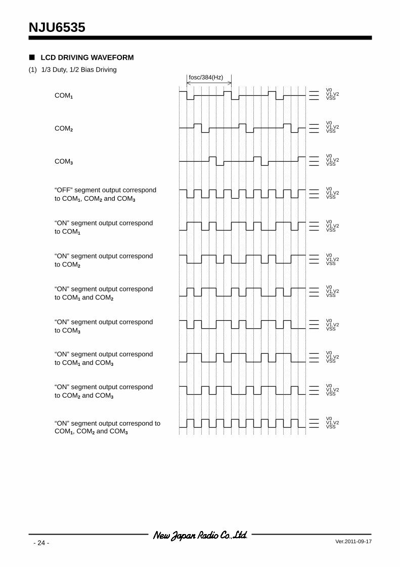
LCD DRIVING WAVEFORM (1) 1/3 Duty, 1/2 Bias Driving
COM1
COM2
COM3
V0 V1,V2 VSS
V0 V1,V2 VSS
V0 V1,V2 VSS
V0 V1,V2 VSS
“OFF” segment output correspond to COM1, COM2 and COM3
“ON” segment output correspond to COM1
V0 V1,V2 VSS
“ON” segment output correspond to COM2
V0 V1,V2 VSS
“ON” segment output correspond to COM1 and COM2
V0 V1,V2 VSS
V0 V1,V2 VSS
“ON” segment output correspond to COM3
V0 V1,V2 VSS
“ON” segment output correspond to COM1 and COM3
V0 V1,V2 VSS
“ON” segment output correspond to COM2 and COM3
V0 V1,V2 VSS “ON” segment output correspond to
COM1, COM2 and COM3
fosc/384(Hz)
NJU6535
- 25 -Ver.2011-09-17
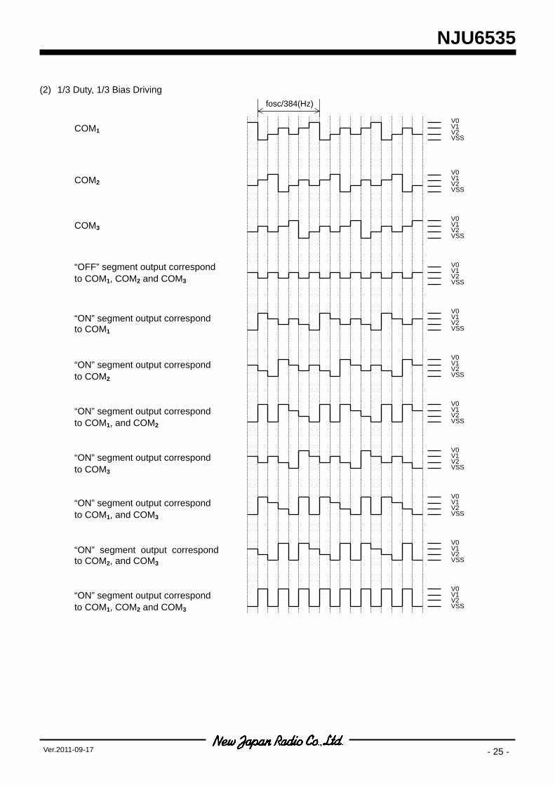
(2) 1/3 Duty, 1/3 Bias Driving
COM1
COM2
COM3
“OFF” segment output correspond to COM1, COM2 and COM3
“ON” segment output correspond to COM1
“ON” segment output correspond to COM2
“ON” segment output correspond to COM1, and COM2
“ON” segment output correspond to COM3
“ON” segment output correspond to COM1, and COM3
“ON” segment output correspondto COM2, and COM3
“ON” segment output correspond to COM1, COM2 and COM3
V0 V1 V2 VSS
V0 V1 V2 VSS
V0 V1 V2 VSS
V0 V1 V2 VSS
V0 V1 V2 VSS
V0 V1 V2 VSS
V0 V1 V2 VSS
V0 V1 V2 VSS
V0 V1 V2 VSS
V0 V1 V2 VSS
V0 V1 V2 VSS
fosc/384(Hz)
NJU6535
- 26 - Ver.2011-09-17
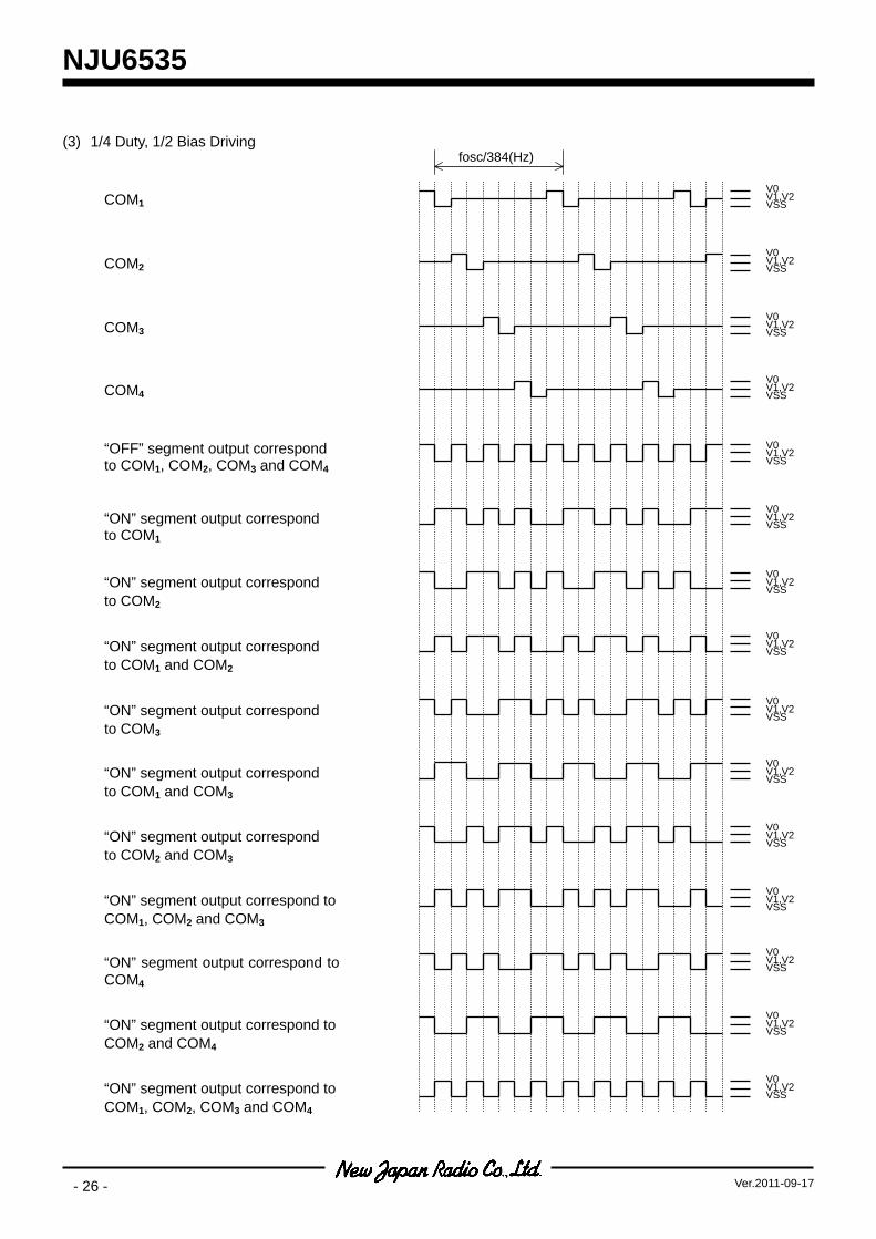
(3) 1/4 Duty, 1/2 Bias Driving
COM1
COM2
COM3
“OFF” segment output correspond to COM1, COM2, COM3 and COM4
“ON” segment output correspond to COM1
“ON” segment output correspond to COM2
“ON” segment output correspond to COM1 and COM2
“ON” segment output correspond to COM3
“ON” segment output correspond to COM1 and COM3
“ON” segment output correspond to COM2 and COM3
“ON” segment output correspond to COM1, COM2 and COM3
COM4
“ON” segment output correspond toCOM4
“ON” segment output correspond to COM2 and COM4
“ON” segment output correspond to COM1, COM2, COM3 and COM4
V0 V1,V2 VSS
V0 V1,V2 VSS
V0 V1,V2 VSS
V0 V1,V2 VSS
V0 V1,V2 VSS
V0 V1,V2 VSS
V0 V1,V2 VSS
V0 V1,V2 VSS
V0 V1,V2 VSS
V0 V1,V2 VSS
V0 V1,V2 VSS
V0 V1,V2 VSS
V0 V1,V2 VSS
V0 V1,V2 VSS
V0 V1,V2 VSS
fosc/384(Hz)
NJU6535
- 27 -Ver.2011-09-17
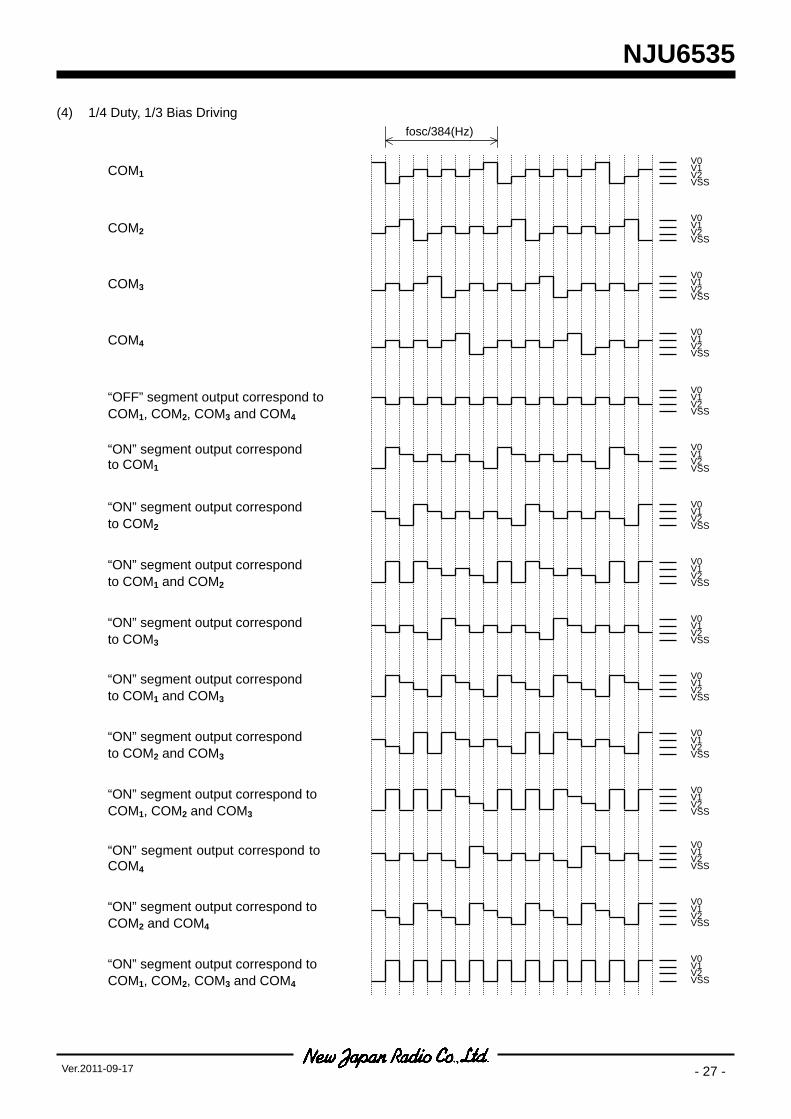
(4) 1/4 Duty, 1/3 Bias Driving
COM1
COM2
COM3
“OFF” segment output correspond to COM1, COM2, COM3 and COM4
V0 V1 V2 VSS
V0 V1 V2 VSS
V0 V1 V2 VSS
V0 V1 V2 VSS
V0 V1 V2 VSS
V0 V1 V2 VSS
V0 V1 V2 VSS
V0 V1 V2 VSS
V0 V1 V2 VSS
V0 V1 V2 VSS
V0 V1 V2 VSS
COM4 V0 V1 V2 VSS
V0 V1 V2 VSS
V0 V1 V2 VSS
V0 V1 V2 VSS
fosc/384(Hz)
“ON” segment output correspond to COM1
“ON” segment output correspond to COM2
“ON” segment output correspond to COM1 and COM2
“ON” segment output correspond to COM3
“ON” segment output correspond to COM1 and COM3
“ON” segment output correspond to COM2 and COM3
“ON” segment output correspond to COM1, COM2 and COM3
“ON” segment output correspond toCOM4
“ON” segment output correspond to COM2 and COM4
“ON” segment output correspond to COM1, COM2, COM3 and COM4
NJU6535
- 28 - Ver.2011-09-17
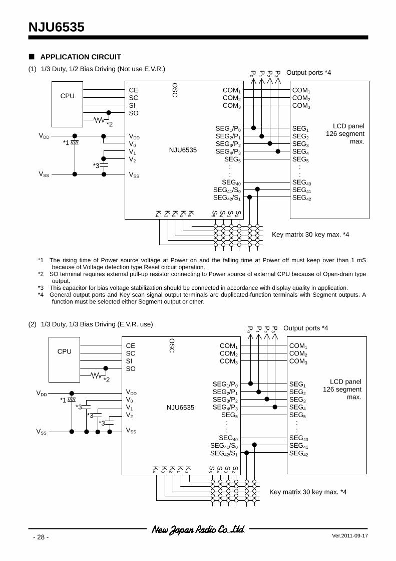
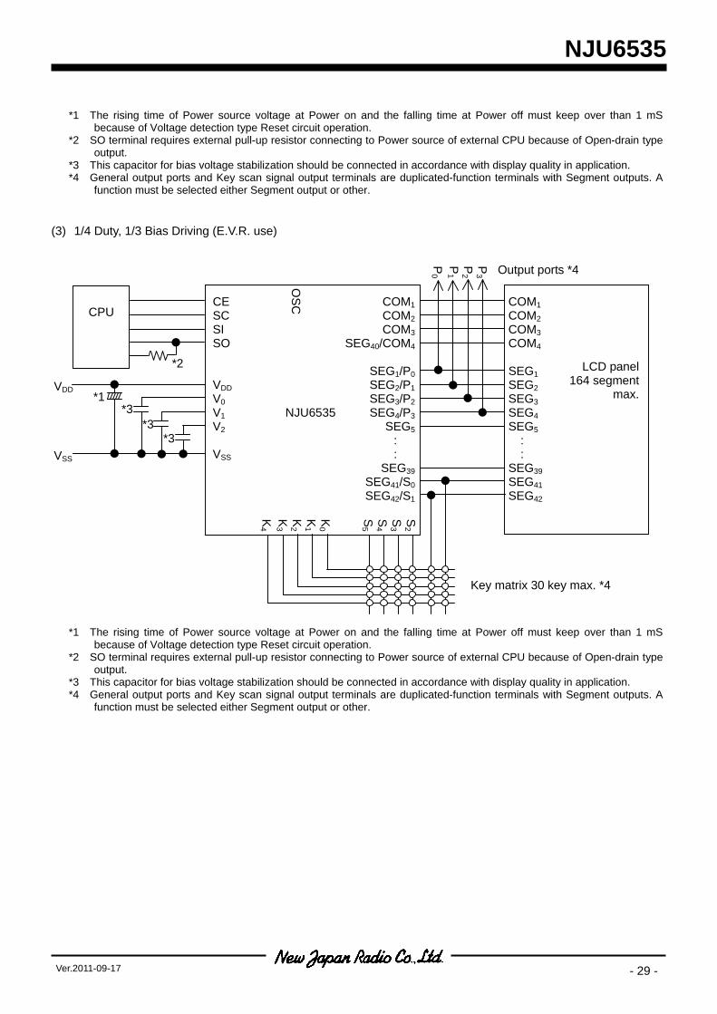
APPLICATION CIRCUIT (1) 1/3 Duty, 1/2 Bias Driving (Not use E.V.R.)
*1 The rising time of Power source voltage at Power on and the falling time at Power off must keep over than 1 mS because of Voltage detection type Reset circuit operation.
*2 SO terminal requires external pull-up resistor connecting to Power source of external CPU because of Open-drain type output.
*3 This capacitor for bias voltage stabilization should be connected in accordance with display quality in application. *4 General output ports and Key scan signal output terminals are duplicated-function terminals with Segment outputs. A
function must be selected either Segment output or other. (2) 1/3 Duty, 1/3 Bias Driving (E.V.R. use)
P3
P2
P1
P0
LCD panel126 segment
max.
COM1COM2COM3
SEG1/P0SEG2/P1SEG3/P2SEG4/P3
SEG5: :
SEG40SEG41/S0SEG42/S1
S2
S3
S4
S5
K0
K1
K2
K3
K4
CPU
CE SC SI SO VDD V0 V1 V2 VSS
*1
*3
COM1 COM2 COM3 SEG1 SEG2 SEG3 SEG4 SEG5
: :
SEG40 SEG41 SEG42
*2
Output ports *4
OS
C
NJU6535
Key matrix 30 key max. *4
VDD VSS
P3
P2
P1
P0
LCD panel126 segment
max.
COM1COM2COM3
SEG1/P0SEG2/P1SEG3/P2SEG4/P3
SEG5: :
SEG40SEG41/S0SEG42/S1
S2
S3
S4
S5
K0
K1
K2
K3
K4
CPU
CE SC SI SO VDD V0 V1 V2 VSS
COM1 COM2 COM3 SEG1 SEG2 SEG3 SEG4 SEG5
: :
SEG40 SEG41 SEG42
*2
Output ports *4
OS
C
*1 *3
*3 *3
NJU6535
Key matrix 30 key max. *4
VDD VSS
NJU6535
- 29 -Ver.2011-09-17
*1 The rising time of Power source voltage at Power on and the falling time at Power off must keep over than 1 mS
because of Voltage detection type Reset circuit operation. *2 SO terminal requires external pull-up resistor connecting to Power source of external CPU because of Open-drain type
output. *3 This capacitor for bias voltage stabilization should be connected in accordance with display quality in application. *4 General output ports and Key scan signal output terminals are duplicated-function terminals with Segment outputs. A
function must be selected either Segment output or other.
(3) 1/4 Duty, 1/3 Bias Driving (E.V.R. use)
*1 The rising time of Power source voltage at Power on and the falling time at Power off must keep over than 1 mS because of Voltage detection type Reset circuit operation.
*2 SO terminal requires external pull-up resistor connecting to Power source of external CPU because of Open-drain type output.
*3 This capacitor for bias voltage stabilization should be connected in accordance with display quality in application. *4 General output ports and Key scan signal output terminals are duplicated-function terminals with Segment outputs. A
function must be selected either Segment output or other.
P3
P2
P1
P0
LCD panel164 segment
max.
COM1COM2COM3
SEG40/COM4
SEG1/P0SEG2/P1SEG3/P2SEG4/P3
SEG5: :
SEG39SEG41/S0SEG42/S1
S2
S3
S4
S5
K0
K1
K2
K3
K4
CPU
CE SC SI SO VDD V0 V1 V2 VSS
*1 *3
*3 *3
COM1 COM2 COM3 COM4 SEG1 SEG2 SEG3 SEG4 SEG5
: :
SEG39 SEG41 SEG42
*2
Output ports *4
OS
CNJU6535
Key matrix 30 key max. *4
VDD VSS
NJU6535
- 30 - Ver.2011-09-17
MEMO
[CAUTION] The specifications on this databook are only
given for information , without any guarantee as regards either mistakes or omissions. Theapplication circuits in this databook are described only to show representative usagesof the product and not intended for the guarantee or permission of any right includingthe industrial rights. The products on this databook may not beappropriate for use in certain equipment wherereliability is critical or where the products maybe subjected to extreme conditions. Thus, youshould consult our sales office before using theproducts in vehicle control equipment.