Embed Size (px)
Citation preview
NiPd Finishes for Pb-Free Leaded Components
Donald C. AbbottTexas Instruments
Attleboro, MA
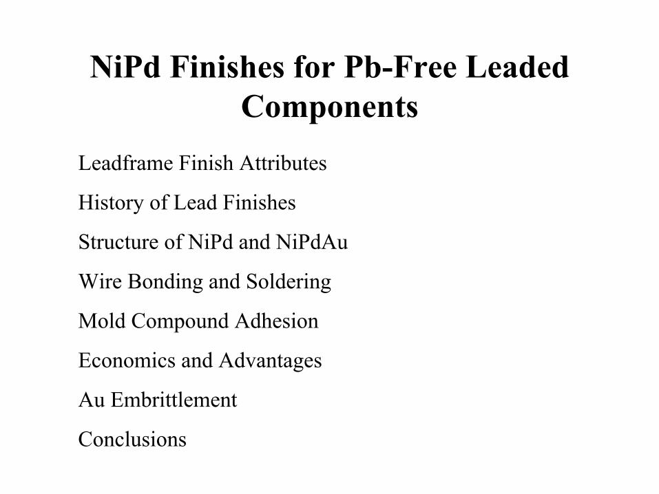
NiPd Finishes for Pb-Free Leaded Components
Leadframe Finish Attributes
History of Lead Finishes
Structure of NiPd and NiPdAu
Wire Bonding and Soldering
Mold Compound Adhesion
Economics and Advantages
Au Embrittlement
Conclusions
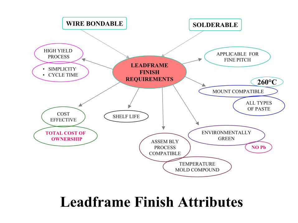
LEADFRAMEFINISH
REQUIREMENTS
WIRE BONDABLE SOLDERABLE
HIGH YIELD PROCESS
COSTEFFECTIVE
SHELF LIFE
ASSEM BLYPROCESS
COMPATIBLE
ENVIRONMENTALLYGREEN
MOUNT COMPATIBLE
APPLICABLE FORFINE PITCH
• SIMPLICITY• CYCLE TIME
TOTAL COST OFOWNERSHIP
TEMPERATUREMOLD COMPOUND
NO Pb
ALL TYPES OF PASTE
Leadframe Finish Attributes
260°C
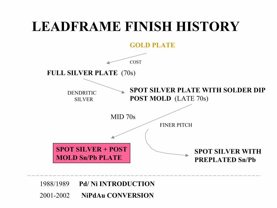
LEADFRAME FINISH HISTORYGOLD PLATE
FULL SILVER PLATE (70s)
SPOT SILVER PLATE WITH SOLDER DIPPOST MOLD (LATE 70s)
FINER PITCH
SPOT SILVER + POSTMOLD Sn/Pb PLATE
SPOT SILVER WITHPREPLATED Sn/Pb
Pd/ Ni INTRODUCTION
MID 70s
1988/1989
COST
DENDRITICSILVER
NiPdAu CONVERSION2001-2002
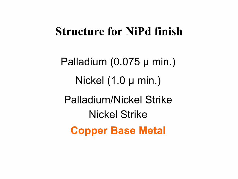
Structure for NiPd finish
Palladium (0.075 µ min.)
Nickel (1.0 µ min.)
Palladium/Nickel StrikeNickel Strike
Copper Base Metal
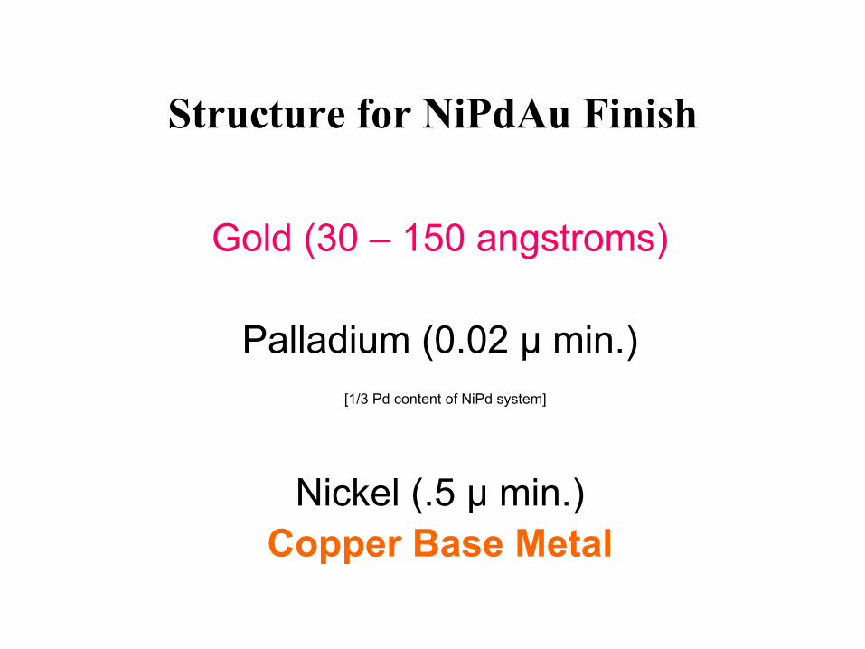
Structure for NiPdAu Finish
Gold (30 – 150 angstroms)
Palladium (0.02 µ min.)[1/3 Pd content of NiPd system]
Nickel (.5 µ min.)Copper Base Metal
Pre-Plated (PPF) v. Post-Mold (PMF) Finish
NiPd is a departure from the Ag spot plating, and has
implications beyond simply the wire bonding and
soldering mechanism differences.
What is the significance of NiPd and NiPdAu?
These are pre-plated finishes (PPF).
The solderable finish is applied at the leadframe maker,
not in a post mold finishing (PMF) operation.
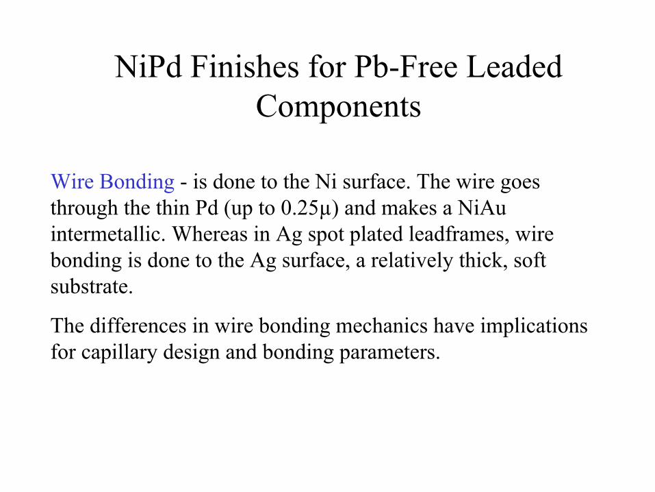
NiPd Finishes for Pb-Free Leaded Components
Wire Bonding - is done to the Ni surface. The wire goes through the thin Pd (up to 0.25µ) and makes a NiAu intermetallic. Whereas in Ag spot plated leadframes, wire bonding is done to the Ag surface, a relatively thick, soft substrate.
The differences in wire bonding mechanics have implications for capillary design and bonding parameters.
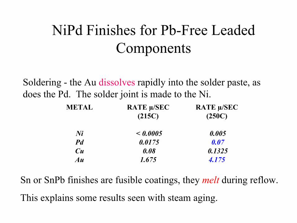
NiPd Finishes for Pb-Free Leaded Components
Soldering - the Au dissolves rapidly into the solder paste, as does the Pd. The solder joint is made to the Ni.
METAL RATE µ/SEC(215C)
RATE µ/SEC(250C)
Ni < 0.0005 0.005Pd 0.0175 0.07Cu 0.08 0.1325Au 1.675 4.175
Sn or SnPb finishes are fusible coatings, they melt during reflow.
This explains some results seen with steam aging.
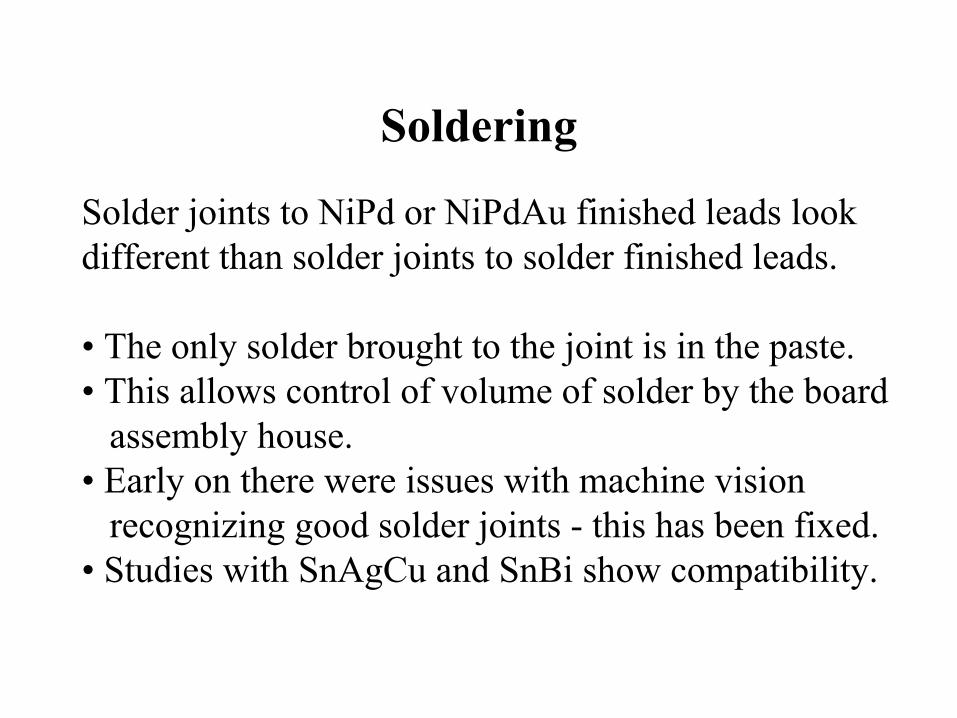
Soldering
Solder joints to NiPd or NiPdAu finished leads lookdifferent than solder joints to solder finished leads.
• The only solder brought to the joint is in the paste.• This allows control of volume of solder by the board
assembly house.• Early on there were issues with machine vision
recognizing good solder joints - this has been fixed.• Studies with SnAgCu and SnBi show compatibility.
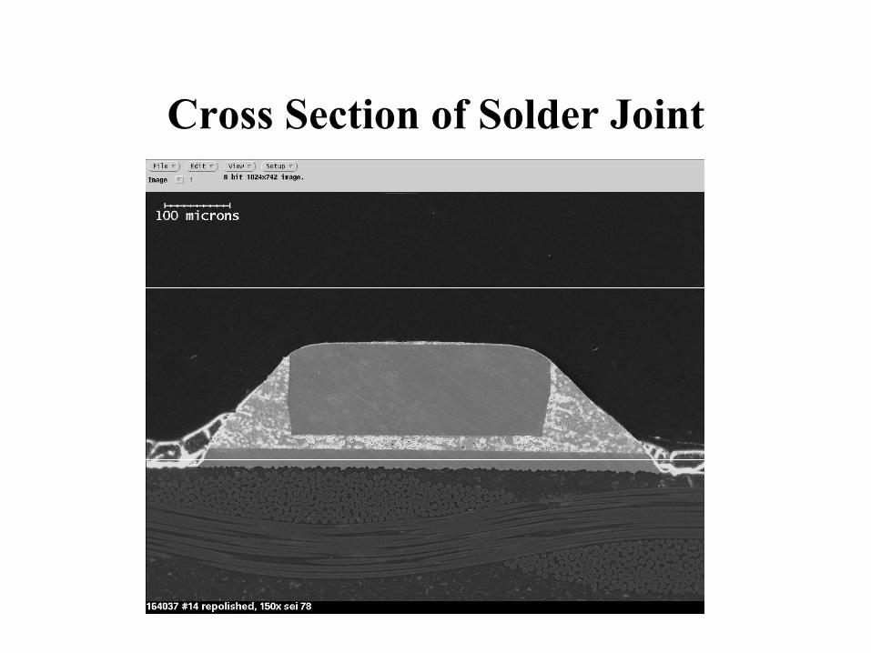
Cross Section of Solder Joint
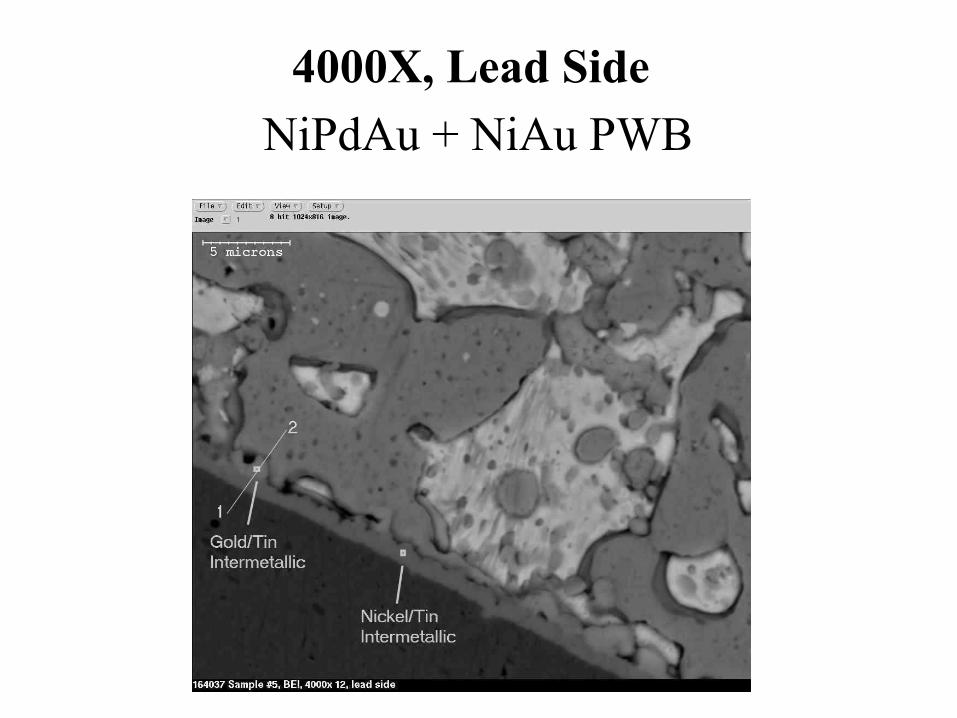
4000X, Lead SideNiPdAu + NiAu PWB
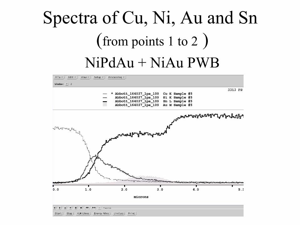
Spectra of Cu, Ni, Au and Sn(from points 1 to 2 )
NiPdAu + NiAu PWB
Mold Compound Adhesion
Mold compound adhesion to Ni substrates and Ag surfaces
has historically been an issue.
Our experience has been that the thin layer of Pd over the
Ni surface enhances mold compound adhesion - with
specific mold compounds.
The advent of 260°C reflow, associated with Pb-free processing, poses a challenge.
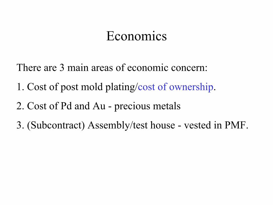
Economics
There are 3 main areas of economic concern:
1. Cost of post mold plating/cost of ownership.
2. Cost of Pd and Au - precious metals
3. (Subcontract) Assembly/test house - vested in PMF.
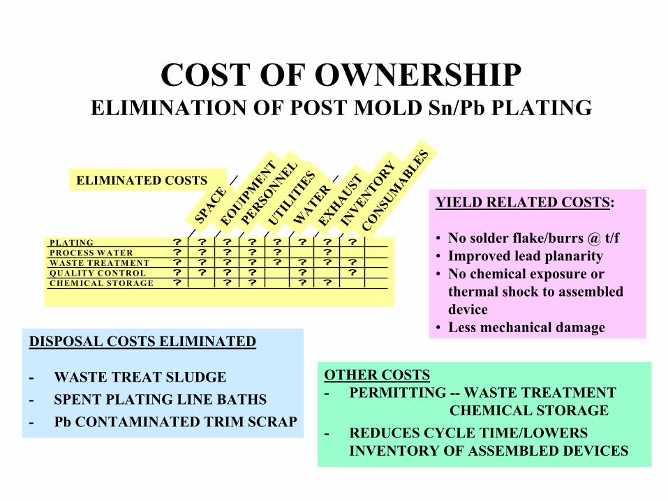
ELIMINATED COSTSSP
ACEEQUIP
MENT
PERSONNEL
UTILIT
IES
WATER
EXHAUSTIN
VENTORY
CONSUM
ABLES
PLATING ? ? ? ? ? ? ? ?PROCESS W ATER ? ? ? ? ? ?W ASTE TREATM ENT ? ? ? ? ? ? ? ?QUALITY CONTROL ? ? ? ? ? ?CHEM ICAL STORAGE ? ? ? ? ?
COST OF OWNERSHIPELIMINATION OF POST MOLD Sn/Pb PLATING
YIELD RELATED COSTS:
• No solder flake/burrs @ t/f• Improved lead planarity• No chemical exposure or
thermal shock to assembled device
• Less mechanical damageDISPOSAL COSTS ELIMINATED
- WASTE TREAT SLUDGE- SPENT PLATING LINE BATHS- Pb CONTAMINATED TRIM SCRAP
OTHER COSTS- PERMITTING -- WASTE TREATMENT
CHEMICAL STORAGE- REDUCES CYCLE TIME/LOWERS
INVENTORY OF ASSEMBLED DEVICES
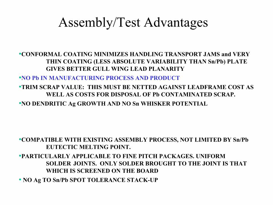
•CONFORMAL COATING MINIMIZES HANDLING TRANSPORT JAMS and VERY THIN COATING (LESS ABSOLUTE VARIABILITY THAN Sn/Pb) PLATE GIVES BETTER GULL WING LEAD PLANARITY
•NO Pb IN MANUFACTURING PROCESS AND PRODUCT•TRIM SCRAP VALUE: THIS MUST BE NETTED AGAINST LEADFRAME COST AS
WELL AS COSTS FOR DISPOSAL OF Pb CONTAMINATED SCRAP.•NO DENDRITIC Ag GROWTH AND NO Sn WHISKER POTENTIAL
Assembly/Test Advantages
•COMPATIBLE WITH EXISTING ASSEMBLY PROCESS, NOT LIMITED BY Sn/Pb EUTECTIC MELTING POINT.
•PARTICULARLY APPLICABLE TO FINE PITCH PACKAGES. UNIFORM SOLDER JOINTS. ONLY SOLDER BROUGHT TO THE JOINT IS THAT WHICH IS SCREENED ON THE BOARD
• NO Ag TO Sn/Pb SPOT TOLERANCE STACK-UP
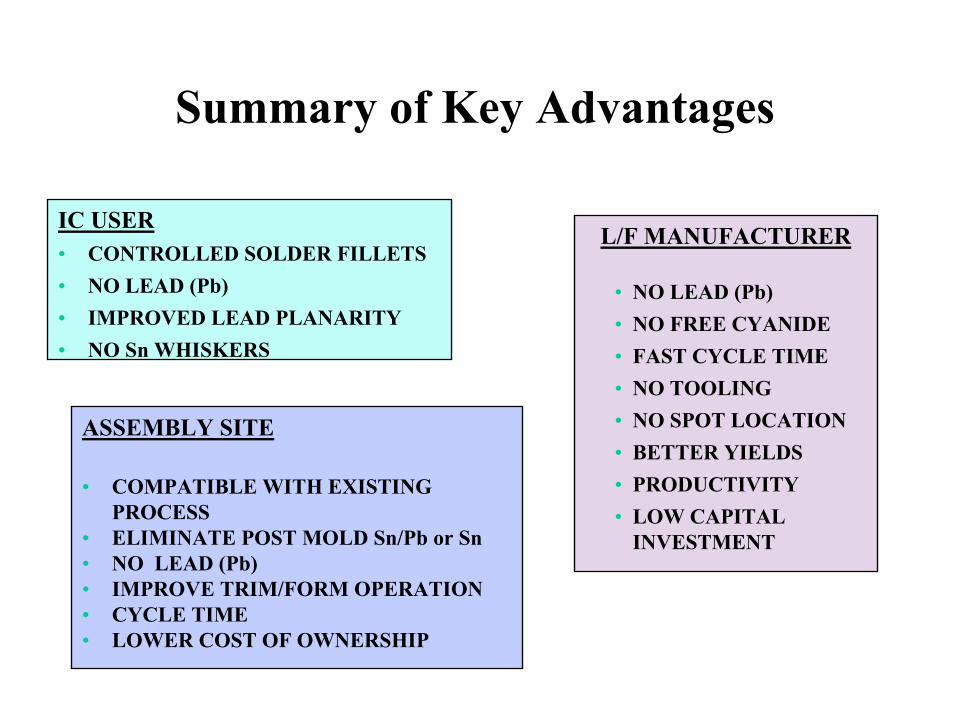
Summary of Key Advantages
IC USER• CONTROLLED SOLDER FILLETS• NO LEAD (Pb)• IMPROVED LEAD PLANARITY• NO Sn WHISKERS
L/F MANUFACTURER
• NO LEAD (Pb)• NO FREE CYANIDE• FAST CYCLE TIME• NO TOOLING• NO SPOT LOCATION• BETTER YIELDS• PRODUCTIVITY• LOW CAPITAL
INVESTMENT
ASSEMBLY SITE
• COMPATIBLE WITH EXISTING PROCESS
• ELIMINATE POST MOLD Sn/Pb or Sn• NO LEAD (Pb)• IMPROVE TRIM/FORM OPERATION• CYCLE TIME• LOWER COST OF OWNERSHIP
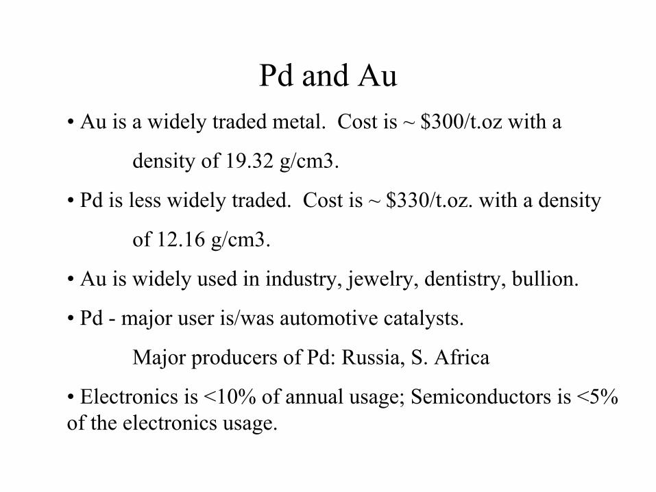
Pd and Au• Au is a widely traded metal. Cost is ~ $300/t.oz with a
density of 19.32 g/cm3.
• Pd is less widely traded. Cost is ~ $330/t.oz. with a density
of 12.16 g/cm3.
• Au is widely used in industry, jewelry, dentistry, bullion.
• Pd - major user is/was automotive catalysts.
Major producers of Pd: Russia, S. Africa
• Electronics is <10% of annual usage; Semiconductors is <5% of the electronics usage.
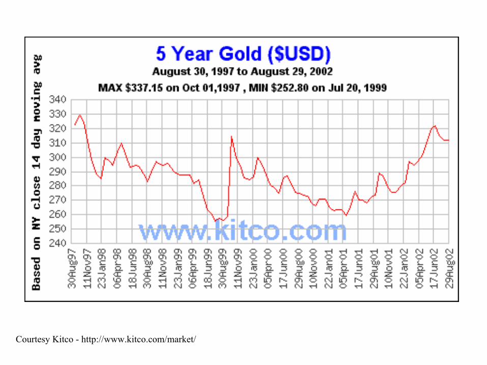
Courtesy Kitco - http://www.kitco.com/market/
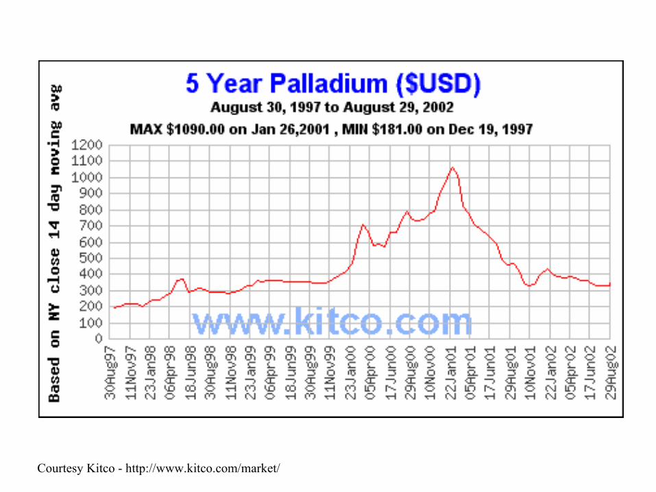
Courtesy Kitco - http://www.kitco.com/market/
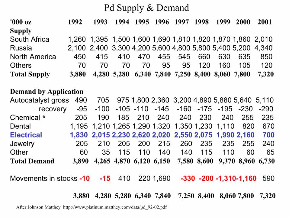
'000 oz 1992 1993 1994 1995 1996 1997 1998 1999 2000 2001SupplySouth Africa 1,260 1,395 1,500 1,600 1,690 1,810 1,820 1,870 1,860 2,010Russia 2,100 2,400 3,300 4,200 5,600 4,800 5,800 5,400 5,200 4,340North America 450 415 410 470 455 545 660 630 635 850Others 70 70 70 70 95 95 120 160 105 120Total Supply 3,880 4,280 5,280 6,340 7,840 7,250 8,400 8,060 7,800 7,320
Demand by ApplicationAutocatalyst gross 490 705 975 1,800 2,360 3,200 4,890 5,880 5,640 5,110
recovery -95 -100 -105 -110 -145 -160 -175 -195 -230 -290Chemical * 205 190 185 210 240 240 230 240 255 235Dental 1,195 1,210 1,265 1,290 1,320 1,350 1,230 1,110 820 670Electrical 1,830 2,015 2,230 2,620 2,020 2,550 2,075 1,990 2,160 700Jewelry 205 210 205 200 215 260 235 235 255 240Other 60 35 115 110 140 140 115 110 60 65Total Demand 3,890 4,265 4,870 6,120 6,150 7,580 8,600 9,370 8,960 6,730
Movements in stocks -10 -15 410 220 1,690 -330 -200 -1,310-1,160 590
3,880 4,280 5,280 6,340 7,840 7,250 8,400 8,060 7,800 7,320After Johnson Matthey http://www.platinum.matthey.com/data/pd_92-02.pdf
Pd Supply & Demand
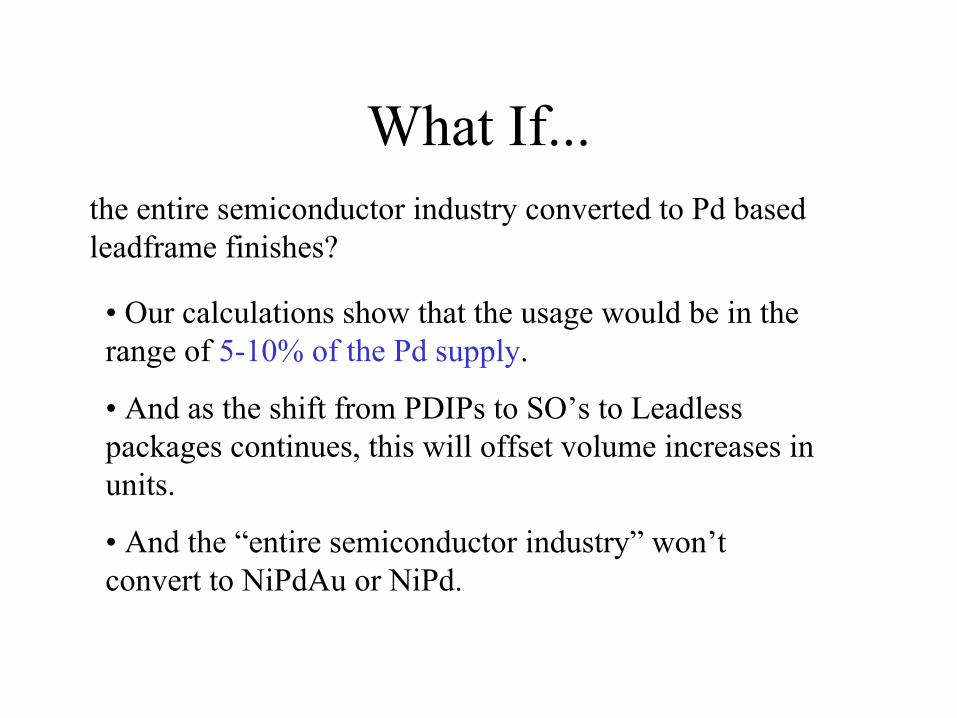
What If...the entire semiconductor industry converted to Pd based leadframe finishes?
• Our calculations show that the usage would be in the range of 5-10% of the Pd supply.
• And as the shift from PDIPs to SO’s to Leadless packages continues, this will offset volume increases in units.
• And the “entire semiconductor industry” won’t convert to NiPdAu or NiPd.
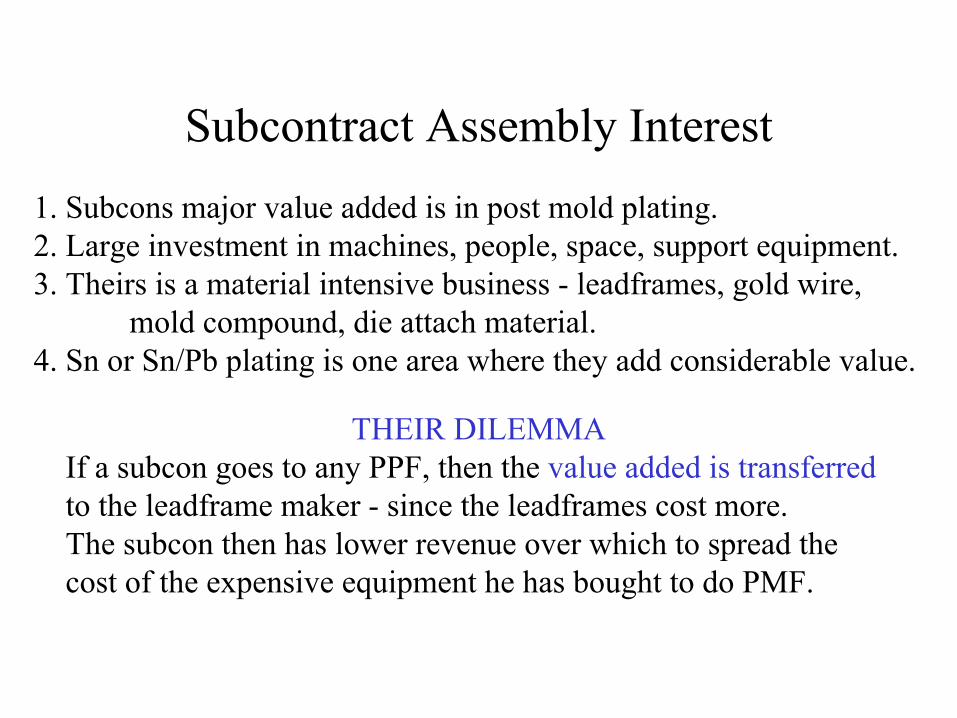
Subcontract Assembly Interest1. Subcons major value added is in post mold plating.2. Large investment in machines, people, space, support equipment.3. Theirs is a material intensive business - leadframes, gold wire,
mold compound, die attach material.4. Sn or Sn/Pb plating is one area where they add considerable value.
THEIR DILEMMAIf a subcon goes to any PPF, then the value added is transferredto the leadframe maker - since the leadframes cost more.The subcon then has lower revenue over which to spread the cost of the expensive equipment he has bought to do PMF.
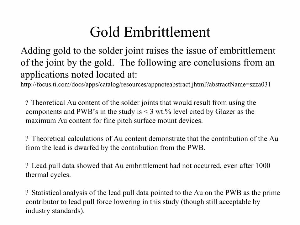
Gold EmbrittlementAdding gold to the solder joint raises the issue of embrittlement of the joint by the gold. The following are conclusions from anapplications noted located at: http://focus.ti.com/docs/apps/catalog/resources/appnoteabstract.jhtml?abstractName=szza031
? Theoretical Au content of the solder joints that would result from using the components and PWB’s in the study is < 3 wt.% level cited by Glazer as the maximum Au content for fine pitch surface mount devices.
? Theoretical calculations of Au content demonstrate that the contribution of the Au from the lead is dwarfed by the contribution from the PWB.
? Lead pull data showed that Au embrittlement had not occurred, even after 1000 thermal cycles.
? Statistical analysis of the lead pull data pointed to the Au on the PWB as the prime contributor to lead pull force lowering in this study (though still acceptable by industry standards).
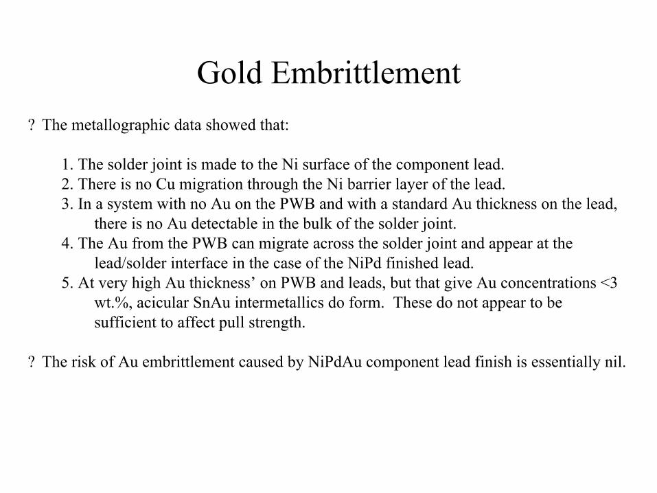
Gold Embrittlement? The metallographic data showed that:
1. The solder joint is made to the Ni surface of the component lead.2. There is no Cu migration through the Ni barrier layer of the lead.3. In a system with no Au on the PWB and with a standard Au thickness on the lead,
there is no Au detectable in the bulk of the solder joint.4. The Au from the PWB can migrate across the solder joint and appear at the
lead/solder interface in the case of the NiPd finished lead.5. At very high Au thickness’ on PWB and leads, but that give Au concentrations <3
wt.%, acicular SnAu intermetallics do form. These do not appear to be sufficient to affect pull strength.
? The risk of Au embrittlement caused by NiPdAu component lead finish is essentially nil.
Conclusions• Pd based lead finishes have been commercialized for >12 years. This is not a “new” technology.
• Given a close to 100% conversion at the A/T site, the economics work.
• There are concerns about the supply/demand of Pd.
• There are no whisker or solderability issues.
• Pd finishes are compatible with Pb-free solders (SnAgCu, SnBi).
![IS 318 (1981): Leaded Tin Bronze Ingots and Castings · IS 318 (1981): Leaded Tin Bronze Ingots and Castings [MTD 8: Copper and Copper Alloys] Title: IS 318 (1981): Leaded Tin Bronze](https://img.pdfslide.us/doc/110x75/5f05e8477e708231d415513f/is-318-1981-leaded-tin-bronze-ingots-and-castings-is-318-1981-leaded-tin-bronze.jpg)