Embed Size (px)
Citation preview
Class E/F Amplifiers
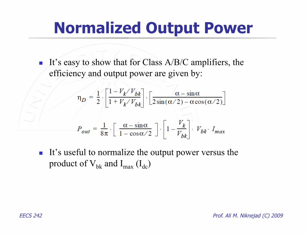
Normalized Output Power
It’s easy to show that for Class A/B/C amplifiers, the efficiency and output power are given by:
It’s useful to normalize the output power versus the product of Vbk and Imax (Idc)
EECS 242 Prof. Ali M. Niknejad (C) 2009
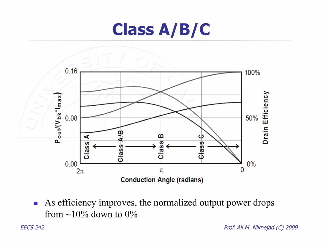
Class A/B/C
As efficiency improves, the normalized output power drops from ~10% down to 0%
EECS 242 Prof. Ali M. Niknejad (C) 2009
Class A/B/C Properties
Keep voltage waveform sinusoidal amplitude is limited to Vdd/2
Only way to improve efficiency is to control current Require very large “on” current to deliver power
EECS 242 Prof. Ali M. Niknejad (C) 2009
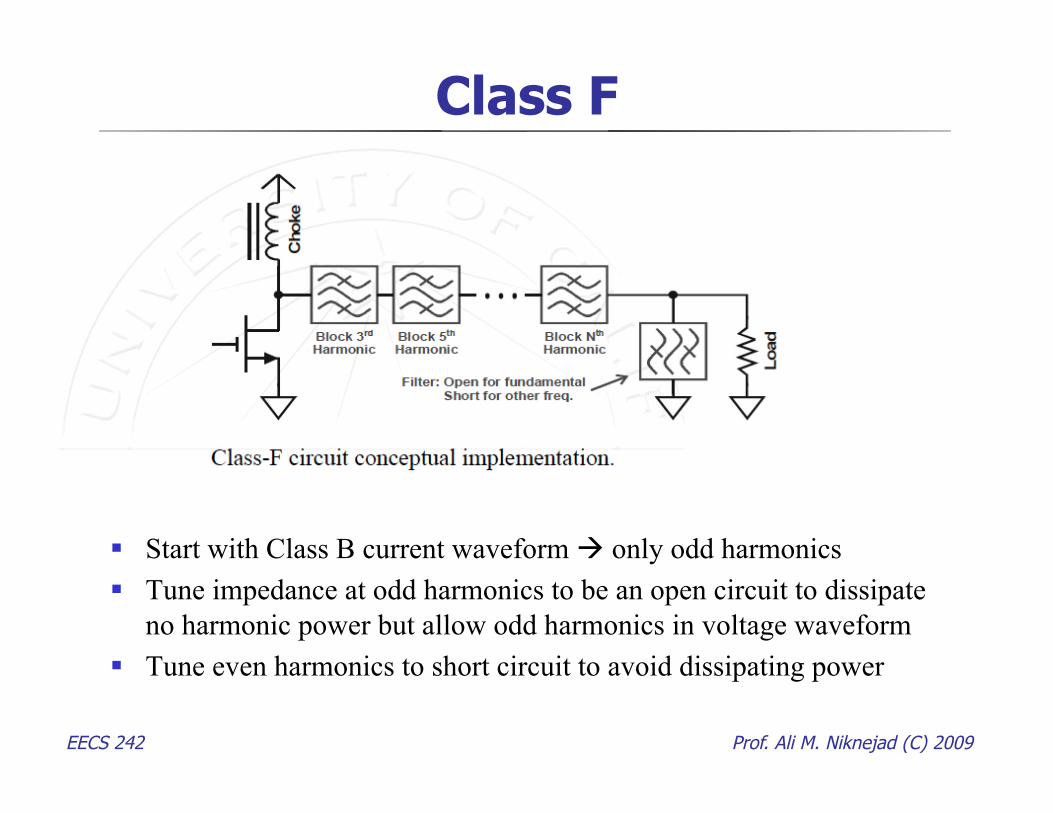
Class F
Start with Class B current waveform only odd harmonics Tune impedance at odd harmonics to be an open circuit to dissipate
no harmonic power but allow odd harmonics in voltage waveform Tune even harmonics to short circuit to avoid dissipating power
EECS 242 Prof. Ali M. Niknejad (C) 2009
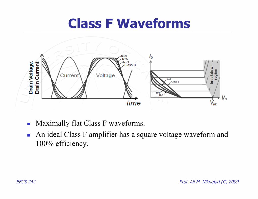
Class F Waveforms
Maximally flat Class F waveforms. An ideal Class F amplifier has a square voltage waveform and
100% efficiency.
EECS 242 Prof. Ali M. Niknejad (C) 2009
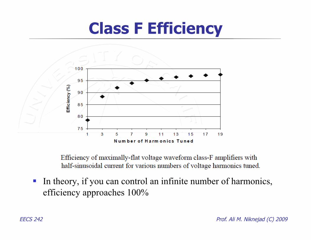
Class F Efficiency
In theory, if you can control an infinite number of harmonics, efficiency approaches 100%
EECS 242 Prof. Ali M. Niknejad (C) 2009
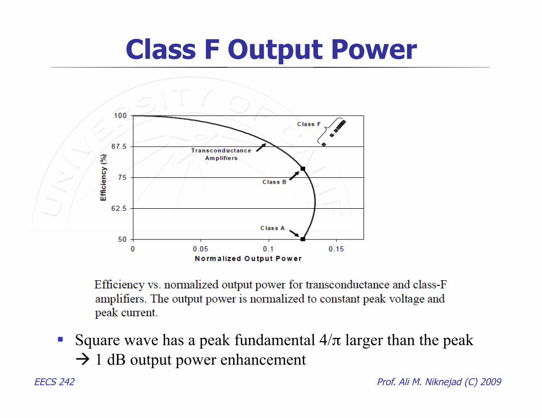
Class F Output Power
Square wave has a peak fundamental 4/π larger than the peak 1 dB output power enhancement
EECS 242 Prof. Ali M. Niknejad (C) 2009
Class F Disadvantages
Output capacitance of device not naturally absorbed into network need inductor to tune it out
Difficult to control more than 5th harmonic … resonators are lossy and additional losses present diminishing returns on efficiency.
EECS 242 Prof. Ali M. Niknejad (C) 2009
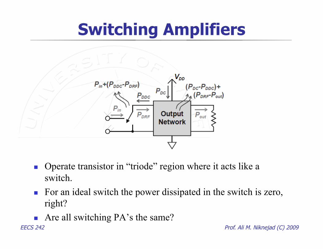
Switching Amplifiers
Operate transistor in “triode” region where it acts like a switch.
For an ideal switch the power dissipated in the switch is zero, right?
Are all switching PA’s the same? EECS 242 Prof. Ali M. Niknejad (C) 2009
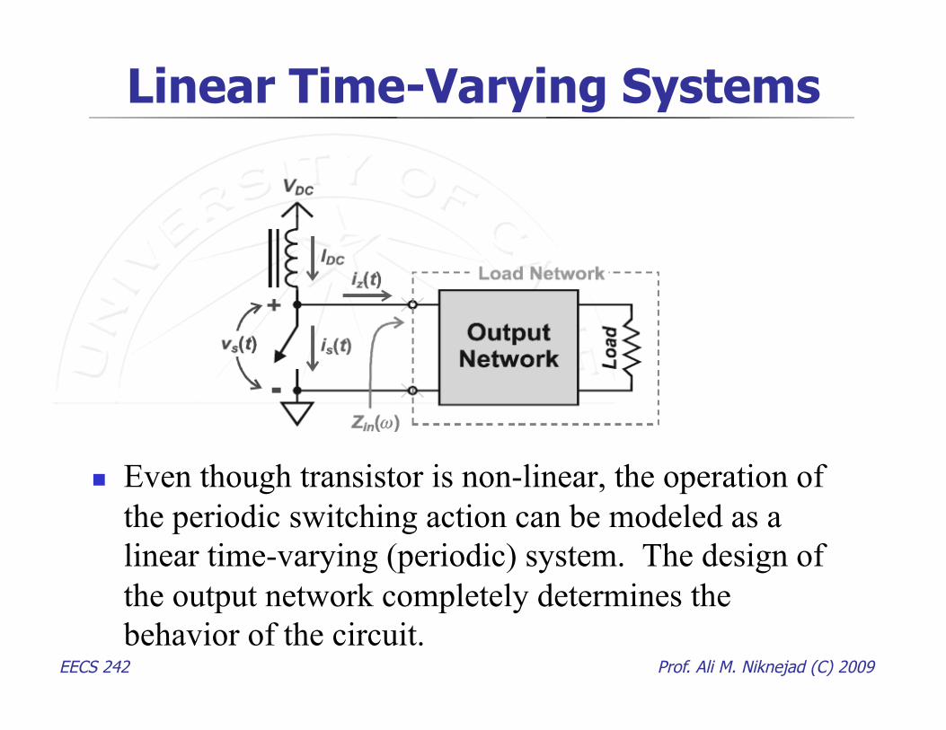
Linear Time-Varying Systems
Even though transistor is non-linear, the operation of the periodic switching action can be modeled as a linear time-varying (periodic) system. The design of the output network completely determines the behavior of the circuit.
EECS 242 Prof. Ali M. Niknejad (C) 2009
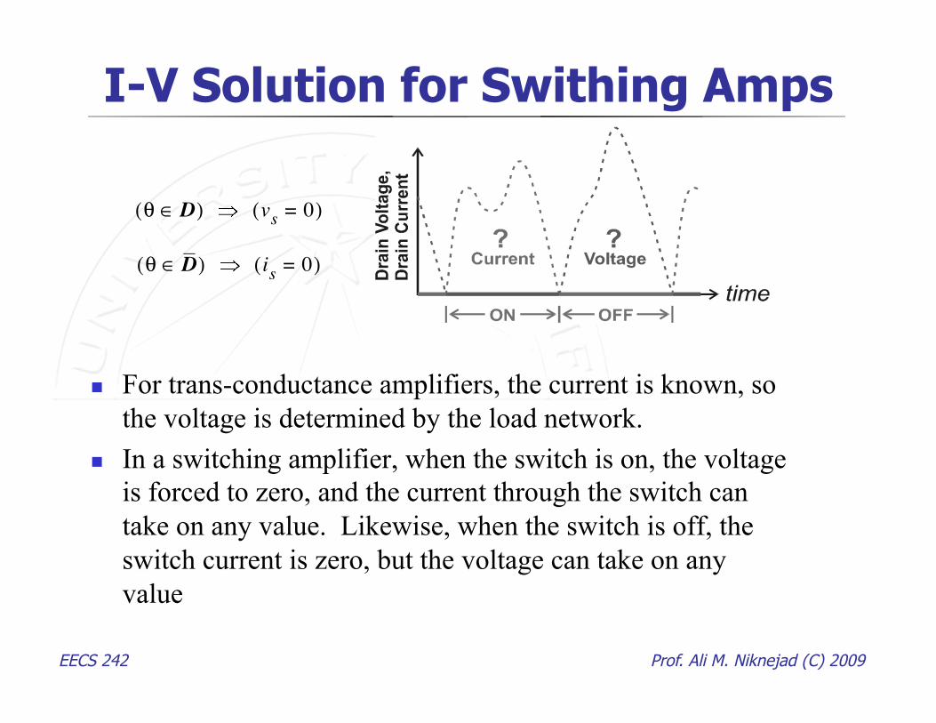
I-V Solution for Swithing Amps
For trans-conductance amplifiers, the current is known, so the voltage is determined by the load network.
In a switching amplifier, when the switch is on, the voltage is forced to zero, and the current through the switch can take on any value. Likewise, when the switch is off, the switch current is zero, but the voltage can take on any value
3.1. Fundamental Operation. 41
network theory. Additionally, if the loss imposed by the switch itself is to determined, the
switch waveforms provide the necessary data for the calculation, as will be shown in the
next chapter.
Unfortunately, the switching waveforms are not found as easily as in the amplifier
classes discussed in Chapter 2. In transconductance amplifiers the current through the
active device is known a priori, and so the voltage waveform is simply the voltage
resulting from that known current forced through the known load impedance. In class-F
amplifiers, the waveforms are assumed to be composed entirely of low-order harmonic
components with simple constraints (such as being maximally flat at a certain point, etc.).
The solution for switching amplifiers is less obvious because the constraint imposed by
the active device is on the voltage waveform for part of the cycle and on the current
waveform for the remainder. Specifically, when the switch is closed the switch voltage vs
is forced to zero, but when open the current is is forced to zero. If the set of times during
which the switch is conducting is denoted D and the set of non-conducting times denoted
D, then these conditions can be written as:
(3.4)
(3.5)
Aside from these two constraints, the switch makes no demands on the waveforms,
and so while the constrained portions of the waveform are trivial to generate, the
unconstrained non-zero portions require additional effort.
It is intuitively obvious that the form of the non-zero portions of the waveform must be
determined somehow by the properties of the load network. The load network is LTI, and
therefore described completely by its frequency-dependent input impedance, and so the
only possible influence it could have on the waveforms is to demanding that, at all
frequencies, the ratio between the voltage and current on its port be equal its port
impedance. Since the waveforms only contain harmonic frequencies, this becomes a
θ D∈( ) vs 0=( )
θ D∈( ) is
0=( )
42 Chapter 3: Switching Amplifier Properties
constraint imposed only at the harmonics. Letting Zin(k) denote the impedance at the kth
harmonic:
(3.6)
Although this condition is easily written down, it is still not obvious how to apply it in
order to determine the waveforms. The difficulty lies in the fact that (3.6) is really an
infinite number of independent frequency domain conditions which must be reconciled
with the very tight time-domain conditions demanded by the switch. Considerable effort
has been exerted to solve for these waveforms even for specific cases such as the myriad
of class-E solutions [4,31-42] each solving for a slightly different circuit topology or using
different approximations and assumptions. Typically the solutions are derived in the time
domain using network theory, utilizing different simplifying assumptions for each
topology, making generalization or comparison difficult. To date, there has been no known
technique for solving this system exactly, although work has been done on solving it under
a finite-harmonic assumption [17].
Figure 3.2: Switching amplifier waveforms after applying switching constraints.
Non-zero values of current and voltage are not yet determined.
vk ik⁄( )ej αk βk–( )
Zin k( )=
k∀ 1 2 3 4 …, , , ,{ }∈
EECS 242 Prof. Ali M. Niknejad (C) 2009
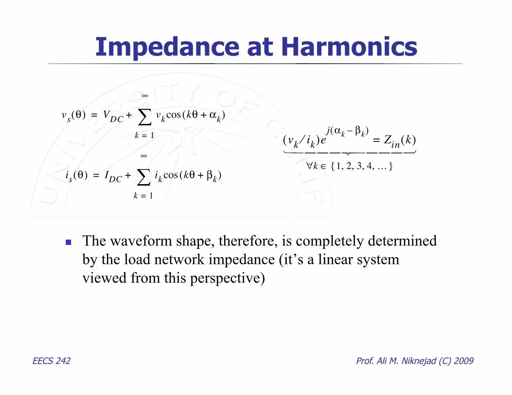
Impedance at Harmonics
The waveform shape, therefore, is completely determined by the load network impedance (it’s a linear system viewed from this perspective)
42 Chapter 3: Switching Amplifier Properties
constraint imposed only at the harmonics. Letting Zin(k) denote the impedance at the kth
harmonic:
(3.6)
Although this condition is easily written down, it is still not obvious how to apply it in
order to determine the waveforms. The difficulty lies in the fact that (3.6) is really an
infinite number of independent frequency domain conditions which must be reconciled
with the very tight time-domain conditions demanded by the switch. Considerable effort
has been exerted to solve for these waveforms even for specific cases such as the myriad
of class-E solutions [4,31-42] each solving for a slightly different circuit topology or using
different approximations and assumptions. Typically the solutions are derived in the time
domain using network theory, utilizing different simplifying assumptions for each
topology, making generalization or comparison difficult. To date, there has been no known
technique for solving this system exactly, although work has been done on solving it under
a finite-harmonic assumption [17].
Figure 3.2: Switching amplifier waveforms after applying switching constraints.
Non-zero values of current and voltage are not yet determined.
vk ik⁄( )ej αk βk–( )
Zin k( )=
k∀ 1 2 3 4 …, , , ,{ }∈
40 Chapter 3: Switching Amplifier Properties
be treated as an effective one-port as indicated by the dashed box in the figure. As such,
the properties of this network are completely specified by its frequency-dependent port
impedance Zin(ω). The circuit’s internal construction is an important implementation
issue, but as far as the operation of the switch is concerned, totally irrelevant
3.1.1 Periodicity
Under the assumption of narrowband operation, the switching pattern will be treated
as being effectively periodic, so that if at any time t0 the switch is in a given state then for
all times the switch is in that same state, for any integer n and for some
fundamental period T. Similarly, the waveforms will be assumed to be periodic, having the
same fundamental period.
By utilizing this assumption, the switch voltage and current waveforms, vs and is
respectively, may be expressed in terms of a Fourier series:
(3.1)
(3.2)
for some values of the parameters VDC, IDC,vk, ik, αk, and βk, and where the normalized
time variable θ is defined as:
(3.3)
3.1.2 Waveform Constraints
The determination the voltages and currents for the a switching amplifier can be
reduced to determining the voltages and currents on the switch itself. Once these
waveforms are known, the other circuit waveforms follow readily using standard linear
nT t0
+
vs
θ( ) VDC
vk
kθ αk
+( )cos
k 1=
∞
+=
is θ( ) IDC ik kθ βk+( )cos
k 1=
∞
+=
θ 2πf0t≡ 2π tT---=
EECS 242 Prof. Ali M. Niknejad (C) 2009
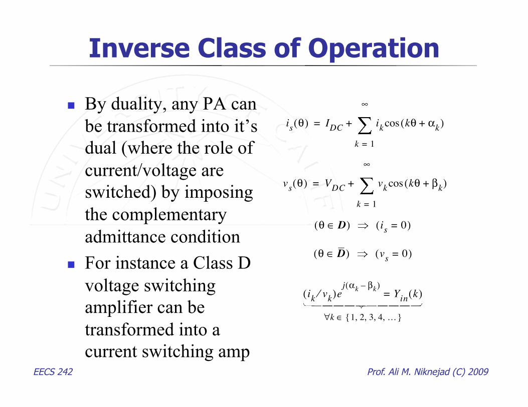
Inverse Class of Operation
By duality, any PA can be transformed into it’s dual (where the role of current/voltage are switched) by imposing the complementary admittance condition
For instance a Class D voltage switching amplifier can be transformed into a current switching amp
44 Chapter 3: Switching Amplifier Properties
linearity has its most obvious effect on the behavior of the circuit for different dc bias
voltages, as will be explored in the next section, but it also allows the seemingly complex
problem of waveform solutions to be stated in the form of a linear algebra problem as will
be shown in Chapter 5.
3.1.4 Complementary Tunings
In developing the waveform constraints in Section 3.1.2, the switching amplifier
solution is converted into a set of mathematical constraints (3.4)-(3.6). In these
expressions, there is a certain symmetry between the current and the voltage. In fact, it is
possible to interchange the role of the current and voltage waveforms, thereby generating
a dual or inverse switching amplifier tuning. This can be done by simply inverting the
drive of the switch (so that the switch will be “on” at times where before it was “off” and
vise-versa) and by using a tuning network presenting, at each harmonic, an input
admittance numerically equal to the original load network’s impedance. To see this more
clearly, consider (3.1)-(3.6) rewritten as follows:
(3.8)
(3.9)
(3.10)
(3.11)
(3.12)
is
θ( ) IDC
ik
kθ αk
+( )cos
k 1=
∞
+=
vs
θ( ) VDC
vk
kθ βk
+( )cos
k 1=
∞
+=
θ D∈( ) is 0=( )
θ D∈( ) vs
0=( )
ikvk
⁄( )ej αk βk–( )
Yink( )=
k∀ 1 2 3 4 …, , , ,{ }∈
EECS 242 Prof. Ali M. Niknejad (C) 2009
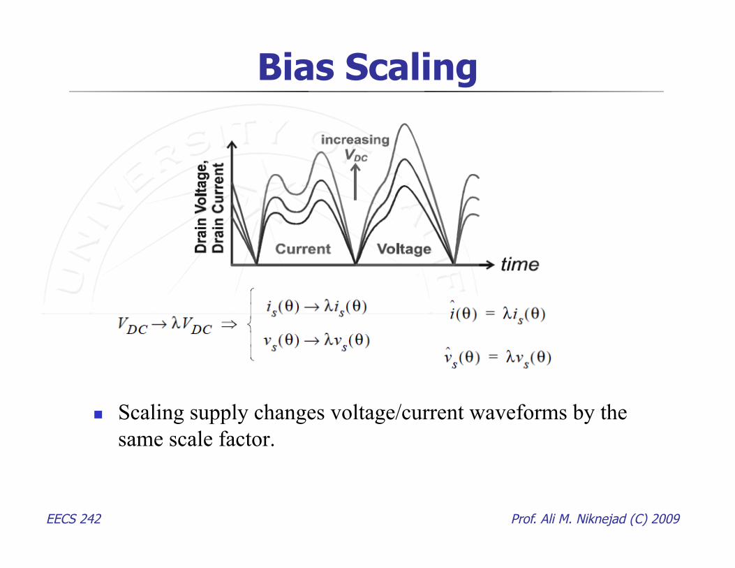
Bias Scaling
Scaling supply changes voltage/current waveforms by the same scale factor.
EECS 242 Prof. Ali M. Niknejad (C) 2009
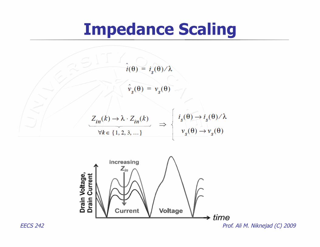
Impedance Scaling
EECS 242 Prof. Ali M. Niknejad (C) 2009
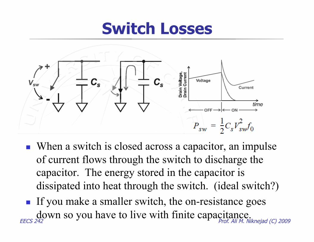
Switch Losses
When a switch is closed across a capacitor, an impulse of current flows through the switch to discharge the capacitor. The energy stored in the capacitor is dissipated into heat through the switch. (ideal switch?)
If you make a smaller switch, the on-resistance goes down so you have to live with finite capacitance.
EECS 242 Prof. Ali M. Niknejad (C) 2009
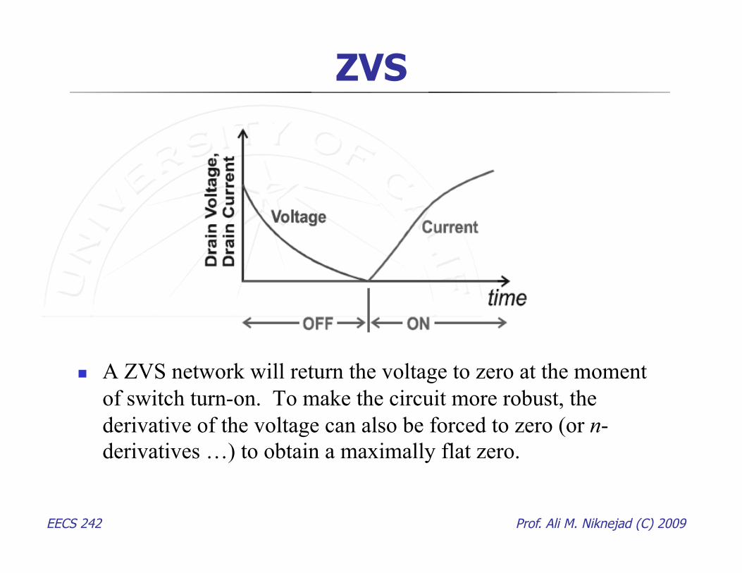
ZVS
A ZVS network will return the voltage to zero at the moment of switch turn-on. To make the circuit more robust, the derivative of the voltage can also be forced to zero (or n-derivatives …) to obtain a maximally flat zero.
EECS 242 Prof. Ali M. Niknejad (C) 2009
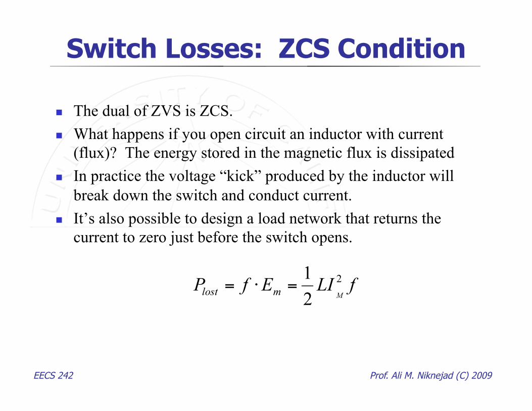
Switch Losses: ZCS Condition
The dual of ZVS is ZCS. What happens if you open circuit an inductor with current
(flux)? The energy stored in the magnetic flux is dissipated In practice the voltage “kick” produced by the inductor will
break down the switch and conduct current. It’s also possible to design a load network that returns the
current to zero just before the switch opens.
EECS 242 Prof. Ali M. Niknejad (C) 2009
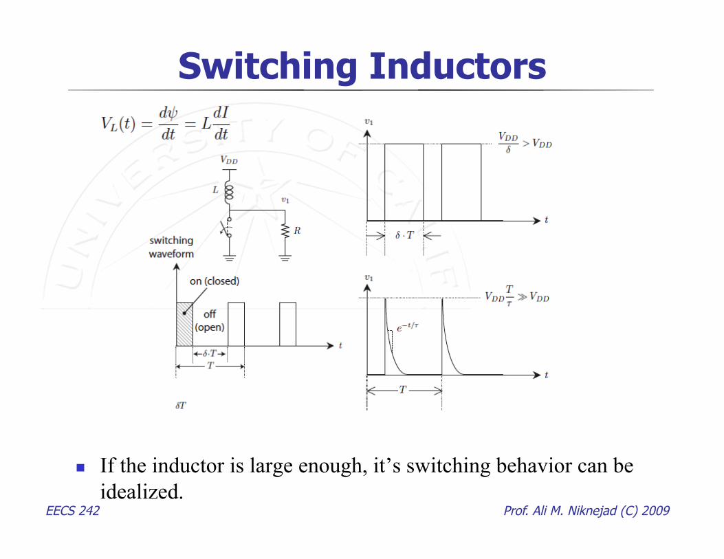
Switching Inductors
If the inductor is large enough, it’s switching behavior can be idealized.
EECS 242 Prof. Ali M. Niknejad (C) 2009
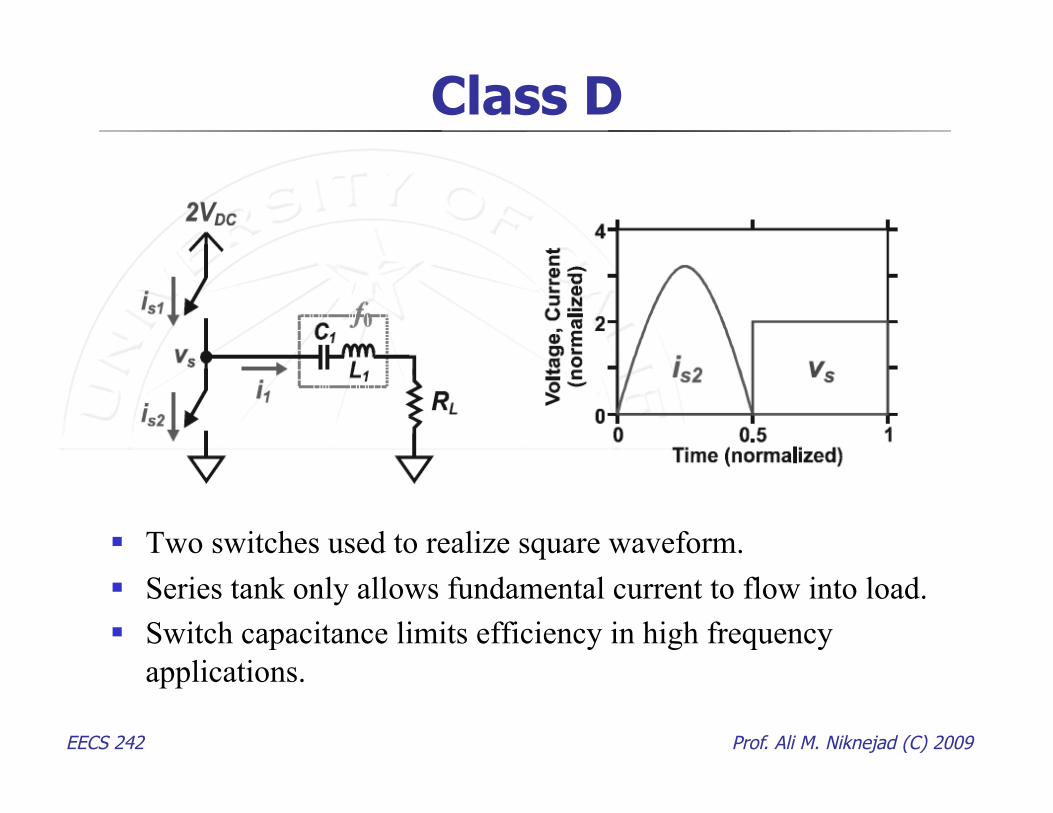
Class D
Two switches used to realize square waveform. Series tank only allows fundamental current to flow into load. Switch capacitance limits efficiency in high frequency
applications.
EECS 242 Prof. Ali M. Niknejad (C) 2009
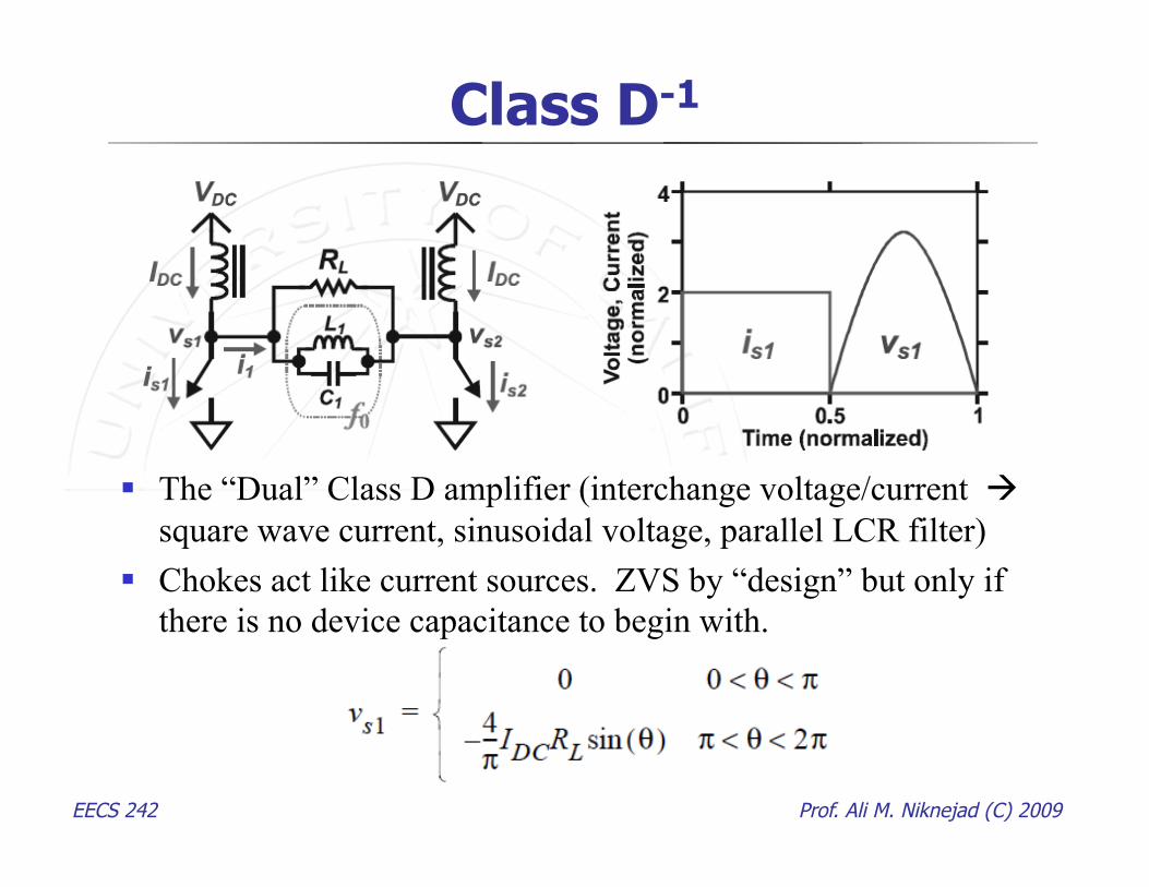
Class D-1
The “Dual” Class D amplifier (interchange voltage/current square wave current, sinusoidal voltage, parallel LCR filter)
Chokes act like current sources. ZVS by “design” but only if there is no device capacitance to begin with.
EECS 242 Prof. Ali M. Niknejad (C) 2009
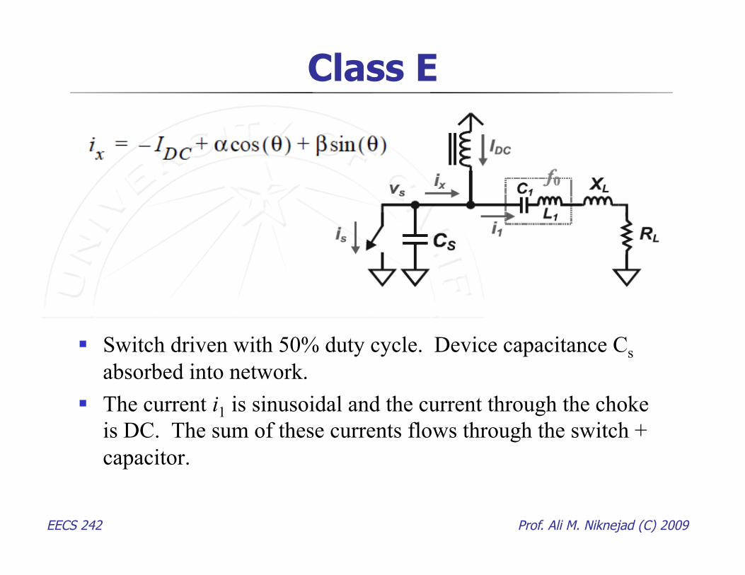
Class E
Switch driven with 50% duty cycle. Device capacitance Cs absorbed into network.
The current i1 is sinusoidal and the current through the choke is DC. The sum of these currents flows through the switch + capacitor.
EECS 242 Prof. Ali M. Niknejad (C) 2009
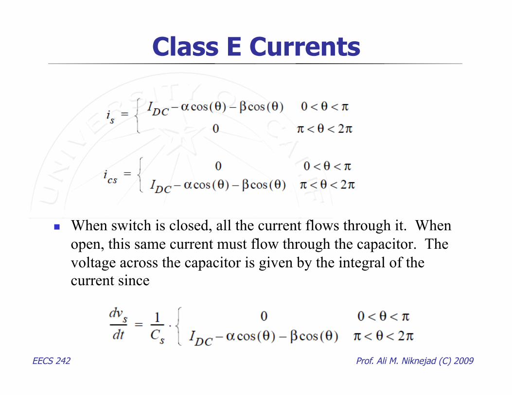
Class E Currents
When switch is closed, all the current flows through it. When open, this same current must flow through the capacitor. The voltage across the capacitor is given by the integral of the current since
EECS 242 Prof. Ali M. Niknejad (C) 2009
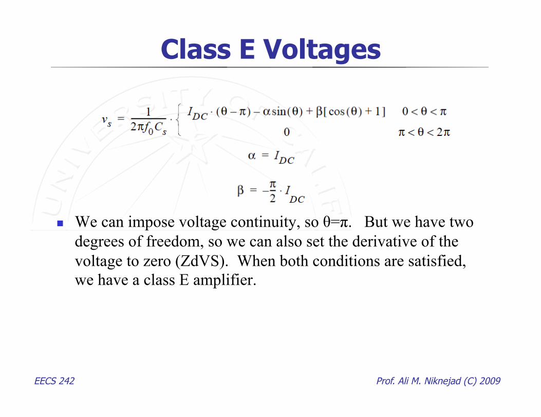
Class E Voltages
We can impose voltage continuity, so θ=π. But we have two degrees of freedom, so we can also set the derivative of the voltage to zero (ZdVS). When both conditions are satisfied, we have a class E amplifier.
EECS 242 Prof. Ali M. Niknejad (C) 2009
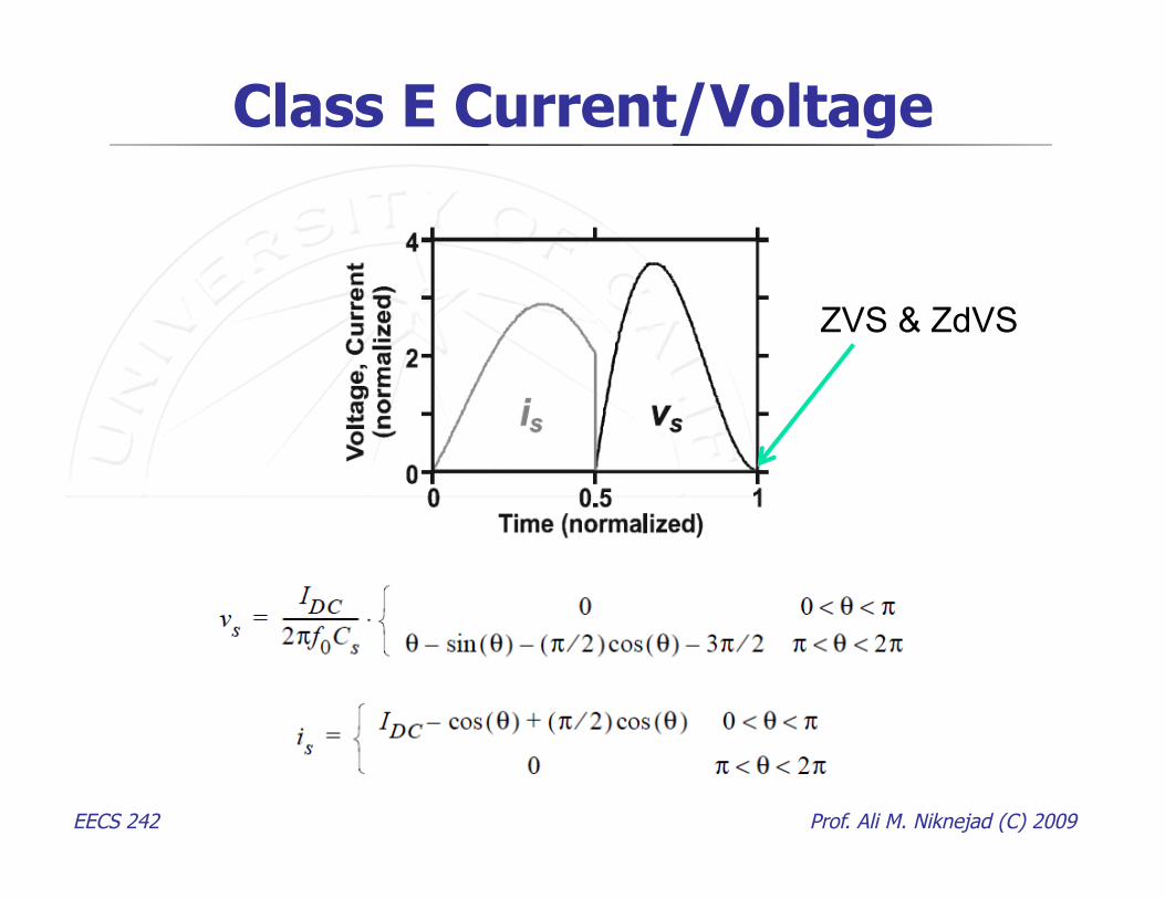
Class E Current/Voltage
ZVS & ZdVS
EECS 242 Prof. Ali M. Niknejad (C) 2009
Class E Load & Swing
The load is given from Fourier analysis of the current/voltage.
To realize a Class E amplifier requires an inductive load. One big disadvantage of the Class E amplifier is that the
voltage swing across the device is very large (nearly 4×VDD).
EECS 242 Prof. Ali M. Niknejad (C) 2009
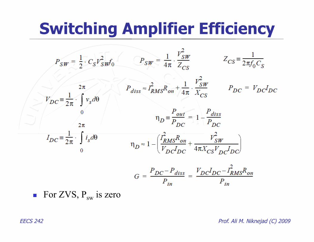
Switching Amplifier Efficiency
For ZVS, Psw is zero
EECS 242 Prof. Ali M. Niknejad (C) 2009
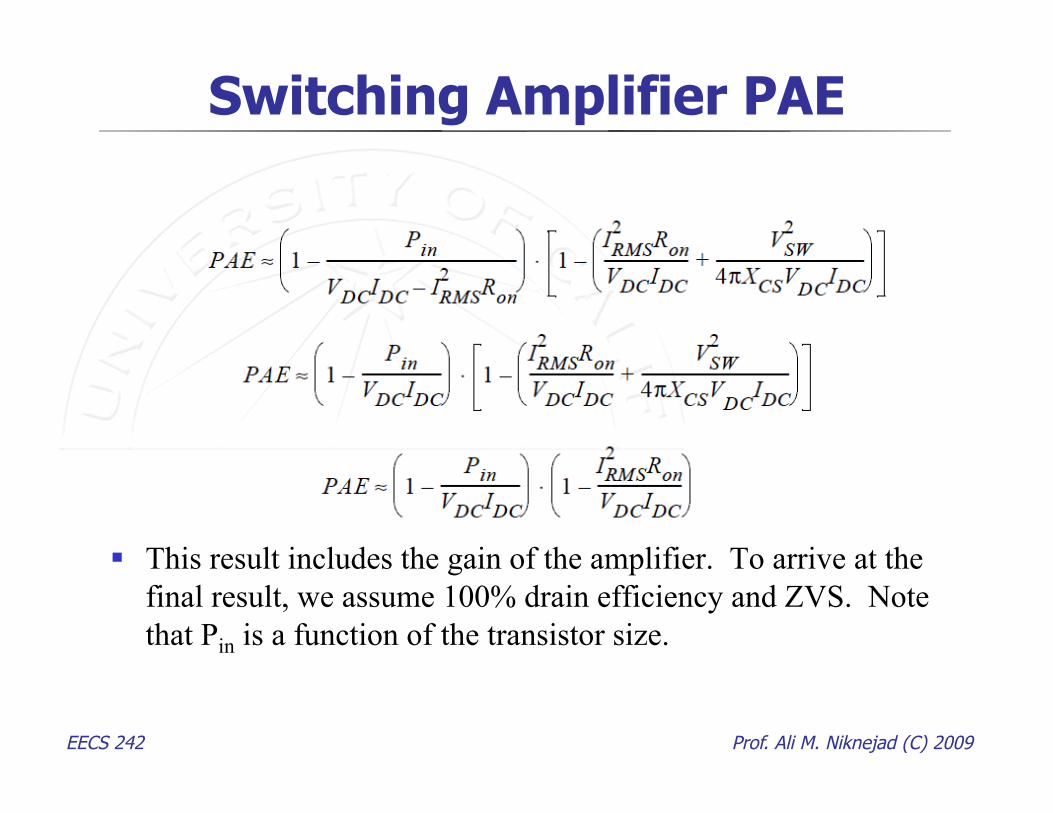
Switching Amplifier PAE
This result includes the gain of the amplifier. To arrive at the final result, we assume 100% drain efficiency and ZVS. Note that Pin is a function of the transistor size.
EECS 242 Prof. Ali M. Niknejad (C) 2009
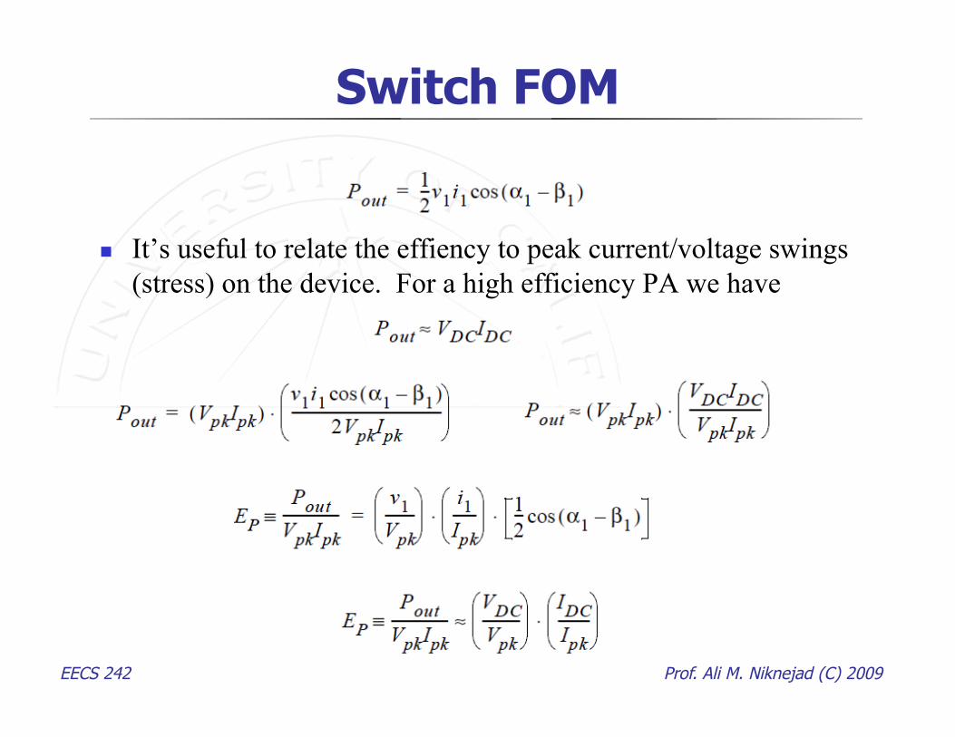
Switch FOM
It’s useful to relate the effiency to peak current/voltage swings (stress) on the device. For a high efficiency PA we have
EECS 242 Prof. Ali M. Niknejad (C) 2009
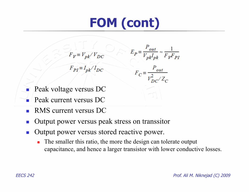
FOM (cont)
Peak voltage versus DC Peak current versus DC RMS current versus DC Output power versus peak stress on transsitor Output power versus stored reactive power.
The smaller this ratio, the more the design can tolerate output capacitance, and hence a larger transistor with lower conductive losses.
EECS 242 Prof. Ali M. Niknejad (C) 2009
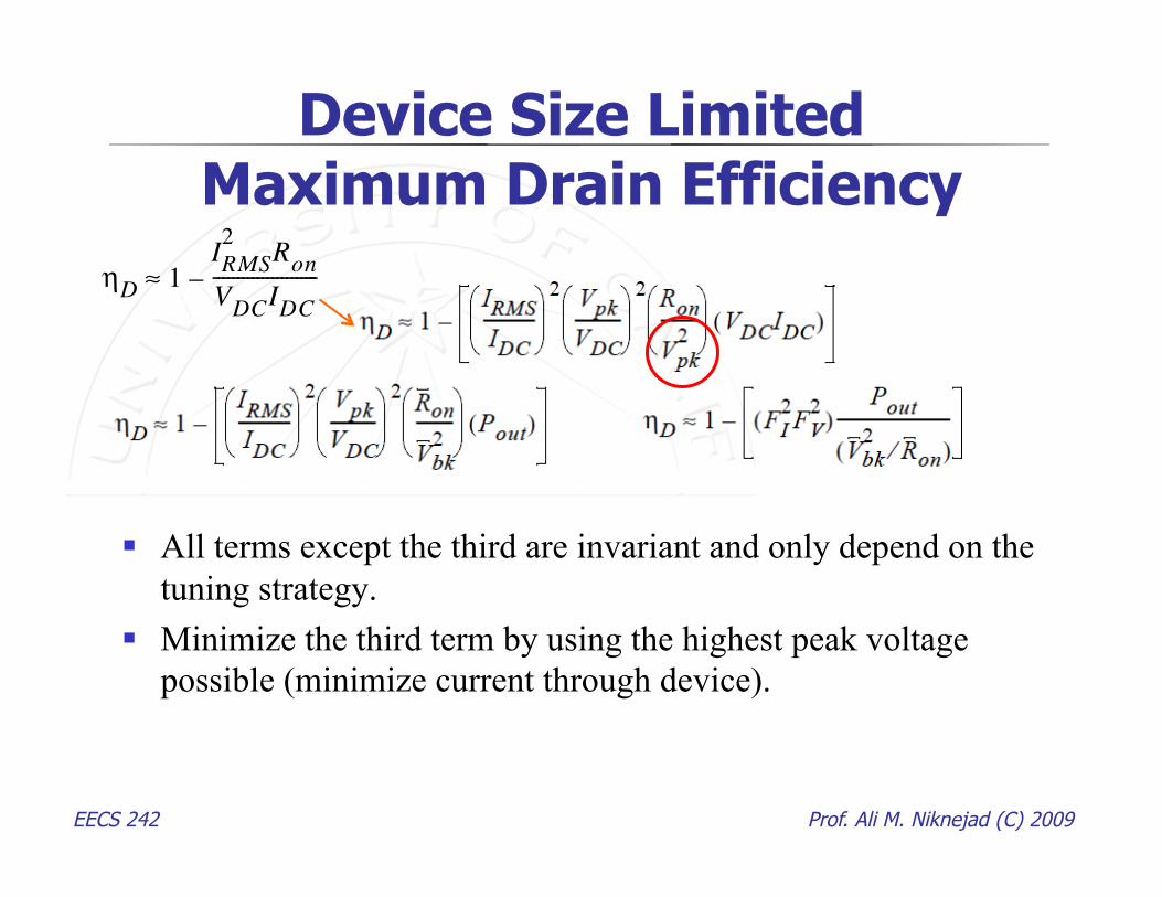
Device Size Limited Maximum Drain Efficiency
All terms except the third are invariant and only depend on the tuning strategy.
Minimize the third term by using the highest peak voltage possible (minimize current through device).
70 Chapter 4: Predicting Switching Amplifier Performance
(4.12)
(4.13)
where vs is the instantaneous drain-source voltage of the FET.
The output power can be determined from energy conservation considerations. If the
switching amplifier has been designed correctly, the power delivered by the transistor to
the load network at the overtone harmonics should be effectively zero. Therefore, the
difference between the power delivered to the transistor from the dc supply and the power
dissipated on the transistor must be the output power:
(4.14)
From this, the drain efficiency can be written as:
(4.15)
Combining this with (4.4) and (4.11), the drain efficiency estimate is found:
(4.16)
which in the ZVS case becomes:
(4.17)
The gain may be found by utilizing (4.14):
(4.18)
VDC1
2π------ vs θd
0
2π
⋅≡
IDC1
2π------ is θd
0
2π
⋅≡
Pout PDC Pdiss–=
ηD
Pout
PDC-----------≡ 1
Pdiss
PDC------------–=
ηD
1IRMS
2Ron
VDCIDC----------------------
VSW
2
4πXCSVDCIDC--------------------------------------+–≈
ηD 1IRMS2
Ron
VDC
IDC
----------------------–≈
GPDC Pdiss–
Pin-----------------------------
VDCIDC IRMS2
Ron–
Pin-------------------------------------------------= =
EECS 242 Prof. Ali M. Niknejad (C) 2009
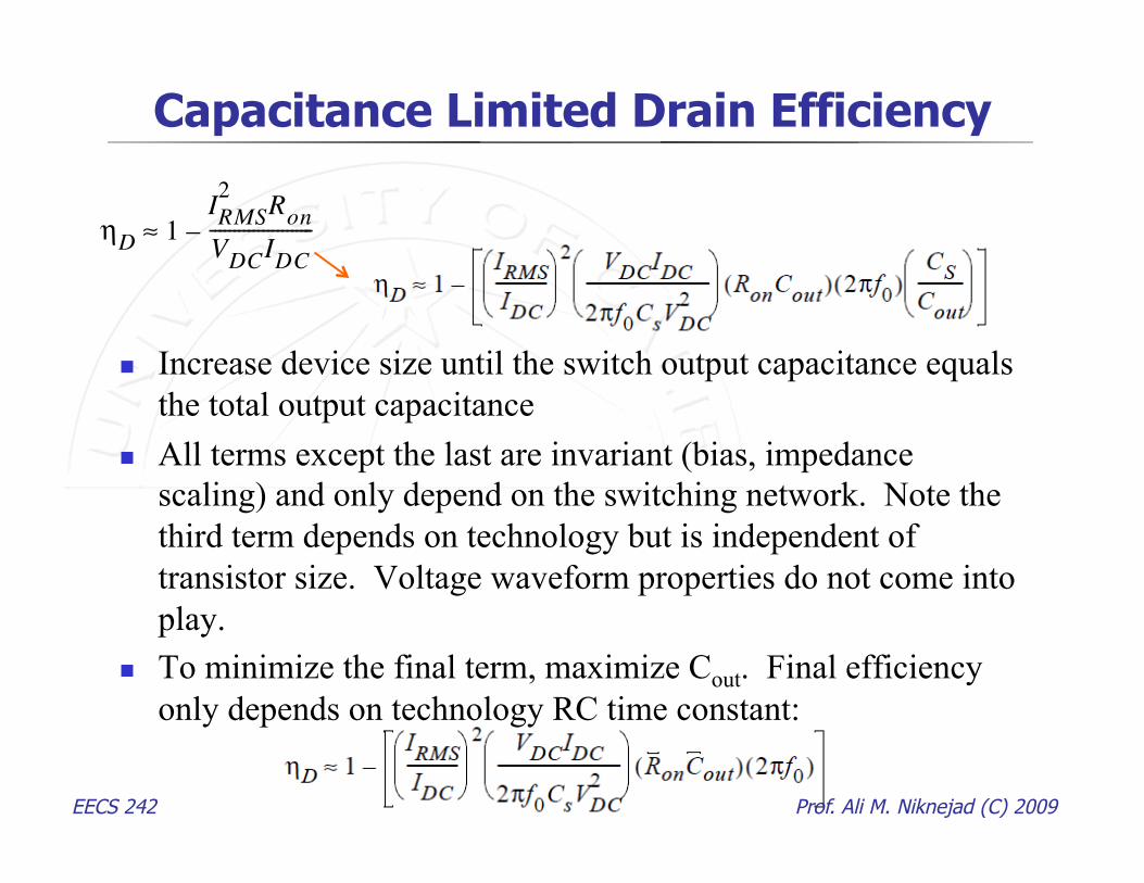
Capacitance Limited Drain Efficiency
Increase device size until the switch output capacitance equals the total output capacitance
All terms except the last are invariant (bias, impedance scaling) and only depend on the switching network. Note the third term depends on technology but is independent of transistor size. Voltage waveform properties do not come into play.
To minimize the final term, maximize Cout. Final efficiency only depends on technology RC time constant:
70 Chapter 4: Predicting Switching Amplifier Performance
(4.12)
(4.13)
where vs is the instantaneous drain-source voltage of the FET.
The output power can be determined from energy conservation considerations. If the
switching amplifier has been designed correctly, the power delivered by the transistor to
the load network at the overtone harmonics should be effectively zero. Therefore, the
difference between the power delivered to the transistor from the dc supply and the power
dissipated on the transistor must be the output power:
(4.14)
From this, the drain efficiency can be written as:
(4.15)
Combining this with (4.4) and (4.11), the drain efficiency estimate is found:
(4.16)
which in the ZVS case becomes:
(4.17)
The gain may be found by utilizing (4.14):
(4.18)
VDC1
2π------ vs θd
0
2π
⋅≡
IDC1
2π------ is θd
0
2π
⋅≡
Pout PDC Pdiss–=
ηD
Pout
PDC-----------≡ 1
Pdiss
PDC------------–=
ηD
1IRMS
2Ron
VDCIDC----------------------
VSW
2
4πXCSVDCIDC--------------------------------------+–≈
ηD 1IRMS2
Ron
VDC
IDC
----------------------–≈
GPDC Pdiss–
Pin-----------------------------
VDCIDC IRMS2
Ron–
Pin-------------------------------------------------= =
EECS 242 Prof. Ali M. Niknejad (C) 2009
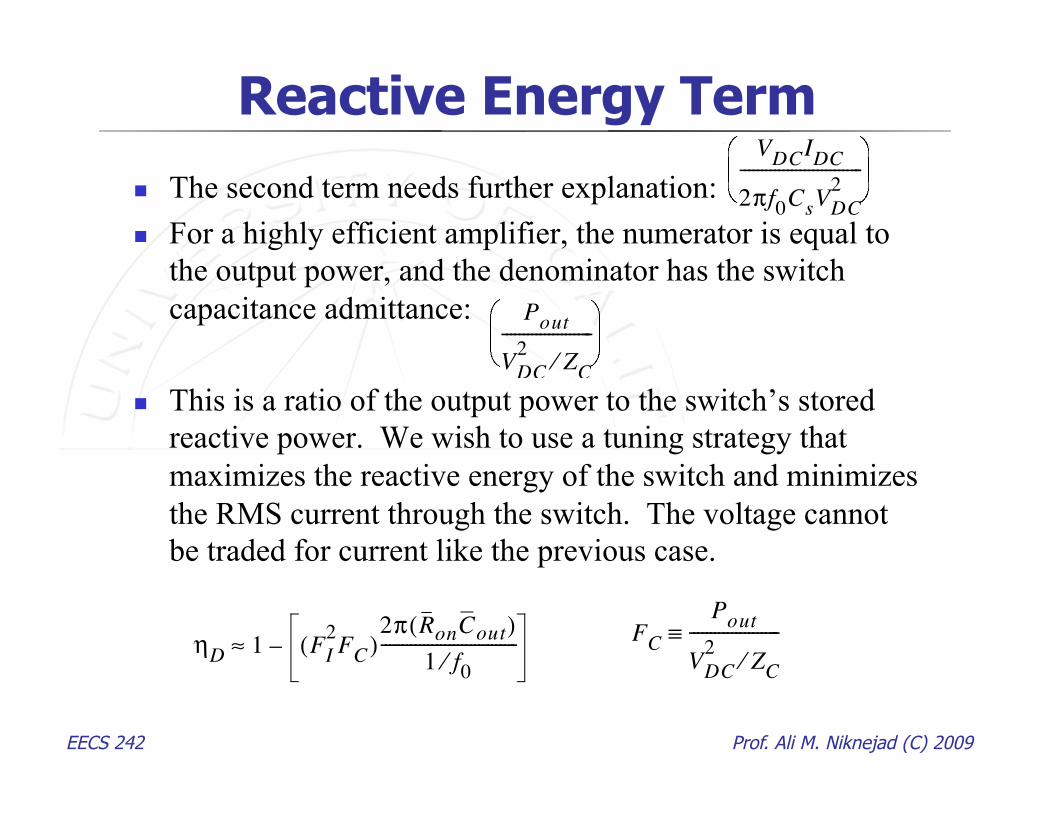
Reactive Energy Term The second term needs further explanation: For a highly efficient amplifier, the numerator is equal to
the output power, and the denominator has the switch capacitance admittance:
This is a ratio of the output power to the switch’s stored reactive power. We wish to use a tuning strategy that maximizes the reactive energy of the switch and minimizes the RMS current through the switch. The voltage cannot be traded for current like the previous case.
76 Chapter 4: Predicting Switching Amplifier Performance
(4.35)
As before, the purpose of this manipulation is to separate the effects of waveform and
transistor technology. The first term is simply the FI waveform figure of merit
encountered earlier. The second term, upon inspection, is also found to be a property of
only the tuning, being invariant under both bias and impedance scaling techniques. The
third term is a function only of the transistor technology, and is invariant under changes in
transistor size. The next term simply indicates that the optimal performance degrades
linearly with increasing frequency.
This leaves the final term, representing the proportion of the switch parallel
capacitance CS made up by the switch's own output capacitance Cout. Since the transistor
size is determined by the designer, this term represents a degree of freedom to be
optimized, under the constraint that Cout cannot be larger than CS. Since the efficiency
improves with increasing Cout, it is clearly best to choose Cout as large as possible. The
optimal sized device is therefore the one with output capacitance equal toCS:
(4.36)
The further illuminate the meaning of the somewhat mysterious second term, consider
that VDCIDC is approximately the equal to the output power and that the is
the magnitude ZC of the switch parallel capacitance’s impedance at the fundamental
frequency:
(4.37)
(4.38)
ηD 1IRMS
IDC
------------
2 VDCIDC
2πf0CsVDC2
----------------------------- RonCout( ) 2πf0( )CS
Cout
-----------–≈
ηD 1IRMS
IDC------------
2 VDC
IDC
2πf0CsVDC2
----------------------------- RonCout( ) 2πf0( )–≈
1 2πf0CS
( )⁄
ηD
1IRMS
IDC
------------
2 Pout
VDC
2ZC
⁄---------------------- RonCout( ) 2πf
0( )–≈
ZC 1 2πf0CS( )⁄≡
4.2. Waveform Figures of Merit 77
Shown this way, the term can be viewed as a ratio between the output power and the
reactive power stored in the capacitance CS. The term measures the tuning strategy's
ability to utilize a large output capacitance (with a high reactive power) without
necessitating a very large output power. A smaller value for this term allows a larger
device size to be used for any given output power, reducing the on-resistance and the
conduction loss.
From (4.37) it may be concluded that it is desirable to have tunings with low RMS to
dc ratio in the current waveforms, and which use a relatively large switch parallel
capacitance to produce a given output power.
Interestingly, the properties of the voltage waveform are of no consequence in this
case. Unlike the previous case where current could be traded for voltage with a resulting
gain in efficiency, increasing the voltage and decreasing the current in this case has no
effect on the efficiency. This is due to the fact that the transistor size is not constant under
this change. In order to trade voltage for current, a combination of impedance and bias
scaling must be used. During this process, the RMS current scales inversely with the
voltage level, whereas the circuit impedances scale proportionally to the square of the
voltage level. The capacitance CS therefore scales inversely with the voltage level. The
transistor size – proportional to CS in this case – must then scale inversely with the square
of the voltage level, causing the on-resistance to scale proportionally to the square of the
voltage level. Thus for an increase in the voltage by a factor of k under the conditions of
constant output power, there is a decrease in the RMS current by a factor of k and an
increase in the on-resistance by a factor of k2. The product therefore stays
constant.
As before, the efficiency may be expressed as waveform figures of merit:
(4.39)
where:
IRMS
2Ron
ηD 1 FI2FC( )
2π RonCout( )1 f0⁄
--------------------------------–≈
78 Chapter 4: Predicting Switching Amplifier Performance
(4.40)
The transistor property of interest in this case is the RonCout product, which is the time
constant of the exponential discharge waveform occurring when the transistor discharges
its own output capacitance. This has units of time, and a desirable transistor technology
would have a very small RonCout time constant relative to the switching period.
4.2.2.3 Gain Limited Power Added Efficiency
The next two cases to be considered are both related to the maximum power added
efficiency (PAE) for a given transistor technology where the designer is free to choose the
optimal sized device. These are similar to the previous case, except that the gain is
considered low enough to be a consideration.
As explored in the previous case, increasing the transistor size results in lower
on-resistance and therefore higher drain efficiency. Unfortunately, this increased transistor
size also results in higher input power. Since the output power is unchanged, the gain
reduces as the transistor size is increased. In cases where the intrinsic device gain is very
high, this may not be an issue and the result of the previous section will be adequate. In
cases where the device gain is not so large, however, a more realistic efficiency measure
such as PAE must be used. The question then becomes how to choose the device size for
best PAE.
Since the drain efficiency increases whereas the gain decreases with increasing device
size, it is not unreasonable to suspect that there is a device size beyond which the
increased drain efficiency is more than offset by the decreased gain. This is in fact the
case, and an amplifier which has reached this point is said to be operating under gain
limited PAE conditions. This minimum may not be achievable, however, since it is
possible that the output capacitance of a device with gain-limited size might exceed the
switch parallel capacitanceCS. Under this capacitance limited condition, the best size will
FC
Pout
VDC2
ZC⁄----------------------≡
EECS 242 Prof. Ali M. Niknejad (C) 2009
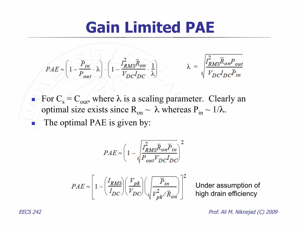
Gain Limited PAE
For Cs = Cout, where λ is a scaling parameter. Clearly an optimal size exists since Ron ~ λ whereas Pin ~ 1/λ.
The optimal PAE is given by:
Under assumption of high drain efficiency
EECS 242 Prof. Ali M. Niknejad (C) 2009
Gain Limited PAE (cont)
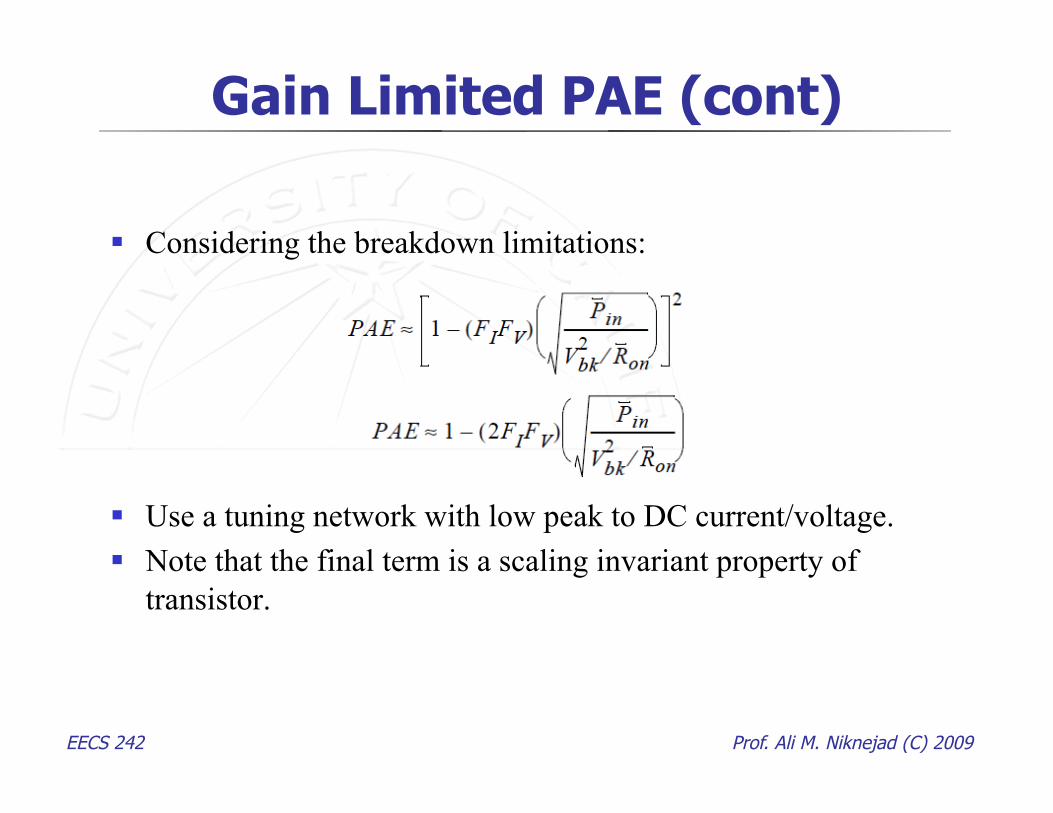
Considering the breakdown limitations:
Use a tuning network with low peak to DC current/voltage. Note that the final term is a scaling invariant property of
transistor.
EECS 242 Prof. Ali M. Niknejad (C) 2009
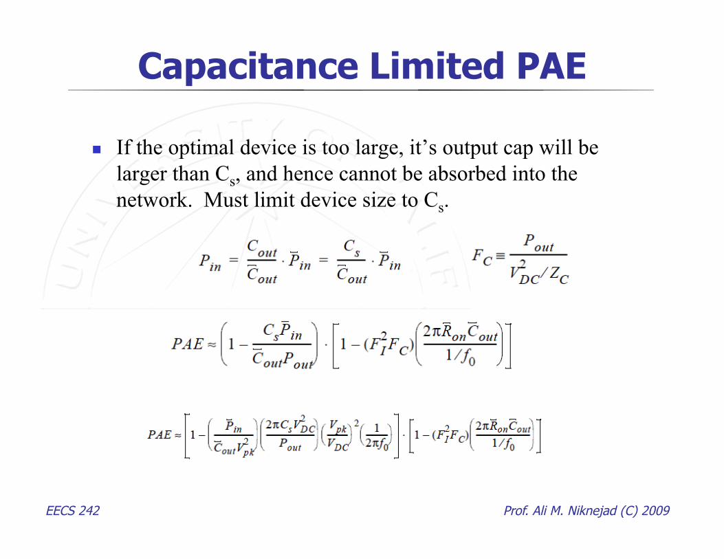
Capacitance Limited PAE
If the optimal device is too large, it’s output cap will be larger than Cs, and hence cannot be absorbed into the network. Must limit device size to Cs.
EECS 242 Prof. Ali M. Niknejad (C) 2009
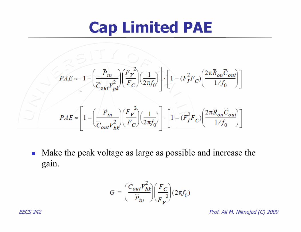
Cap Limited PAE
Make the peak voltage as large as possible and increase the gain.
EECS 242 Prof. Ali M. Niknejad (C) 2009
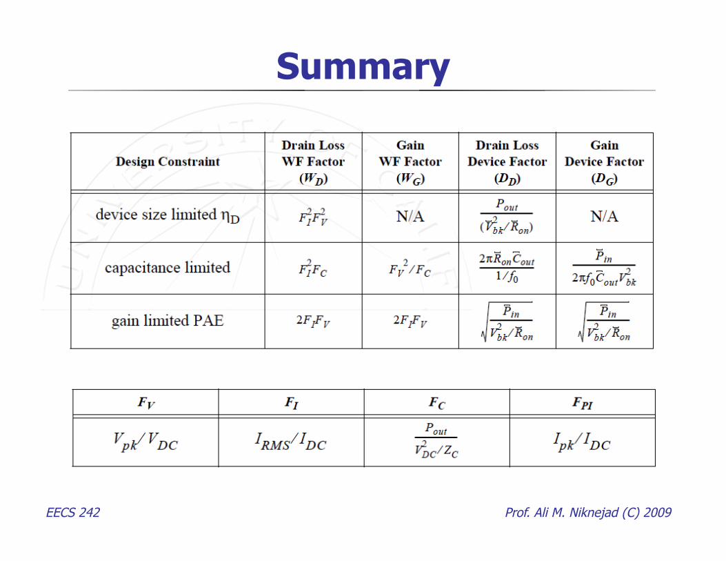
Summary
EECS 242 Prof. Ali M. Niknejad (C) 2009
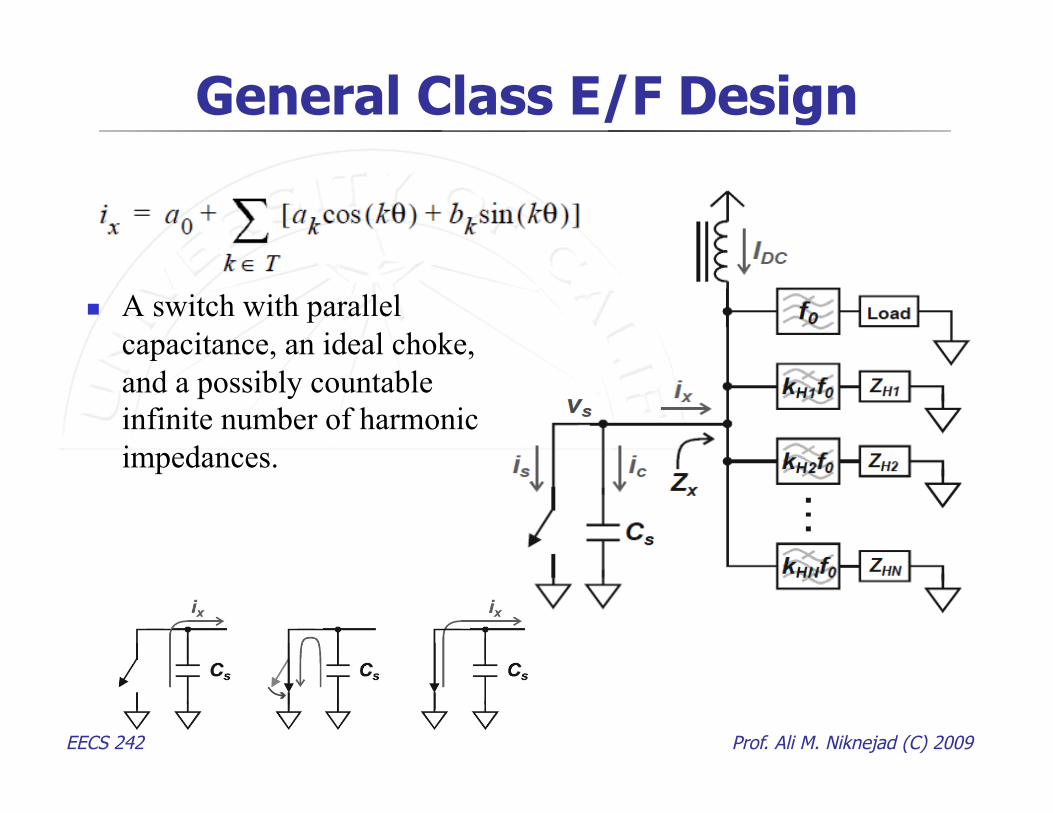
General Class E/F Design
A switch with parallel capacitance, an ideal choke, and a possibly countable infinite number of harmonic impedances.
EECS 242 Prof. Ali M. Niknejad (C) 2009
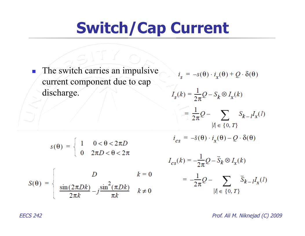
Switch/Cap Current
The switch carries an impulsive current component due to cap discharge.
EECS 242 Prof. Ali M. Niknejad (C) 2009
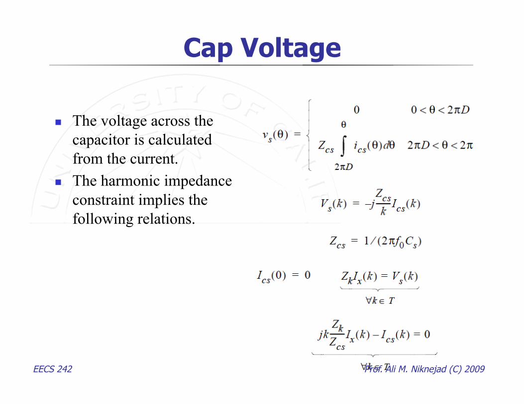
Cap Voltage
The voltage across the capacitor is calculated from the current.
The harmonic impedance constraint implies the following relations.
EECS 242 Prof. Ali M. Niknejad (C) 2009
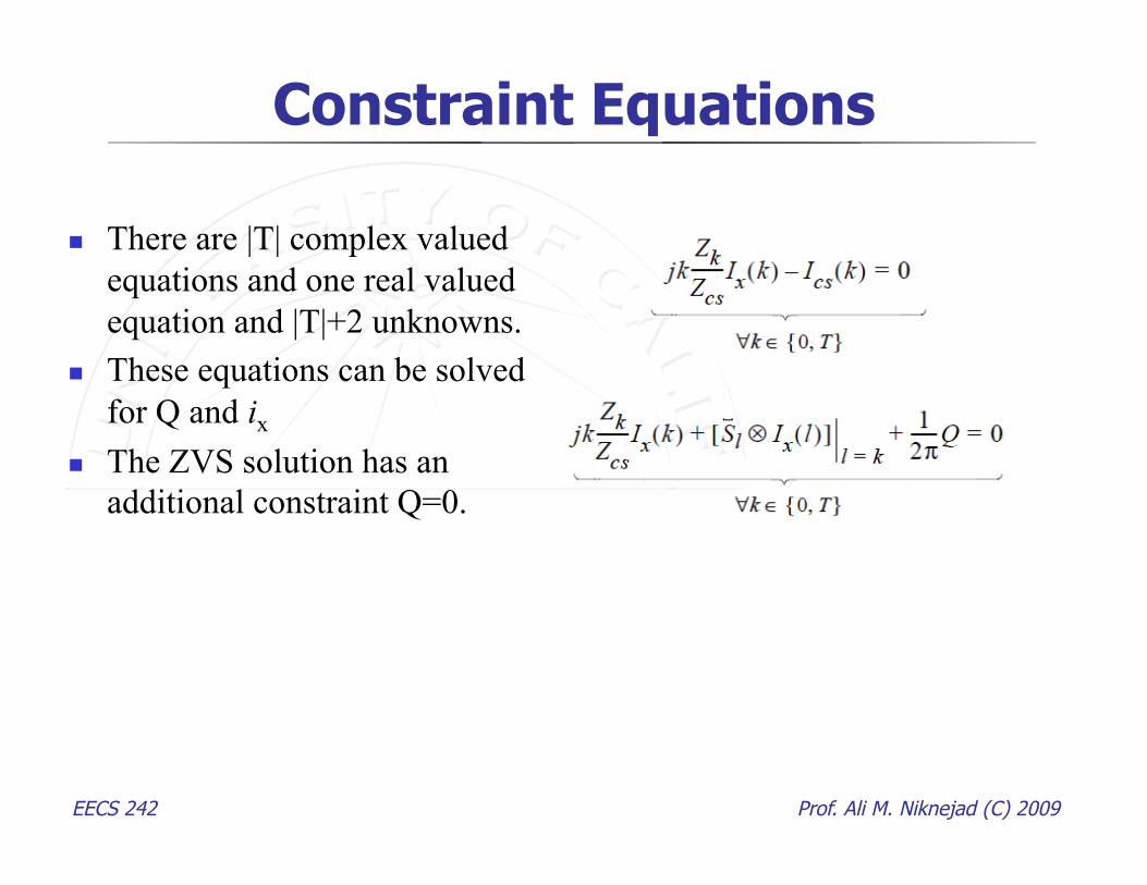
Constraint Equations
There are |T| complex valued equations and one real valued equation and |T|+2 unknowns.
These equations can be solved for Q and ix
The ZVS solution has an additional constraint Q=0.
EECS 242 Prof. Ali M. Niknejad (C) 2009
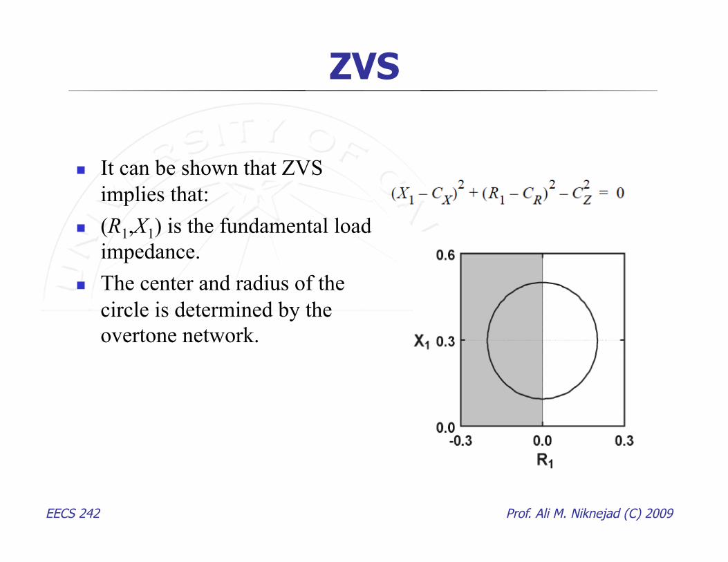
ZVS
It can be shown that ZVS implies that:
(R1,X1) is the fundamental load impedance.
The center and radius of the circle is determined by the overtone network.
EECS 242 Prof. Ali M. Niknejad (C) 2009
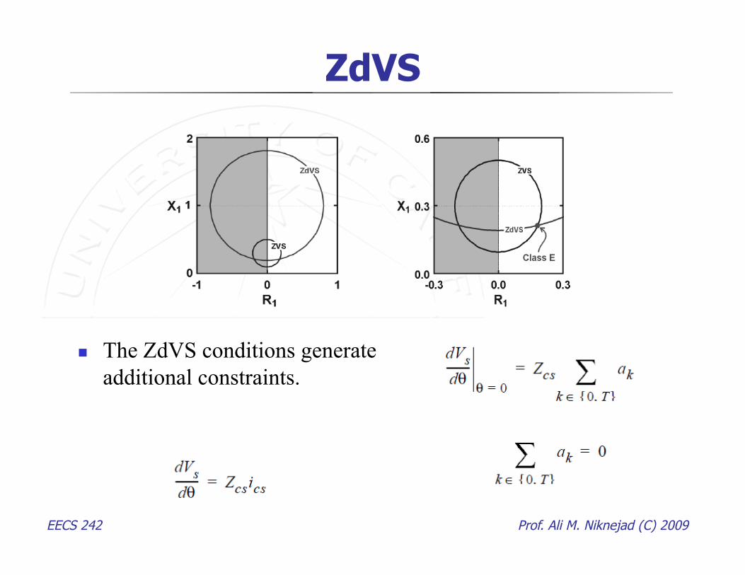
ZdVS
The ZdVS conditions generate additional constraints.
EECS 242 Prof. Ali M. Niknejad (C) 2009
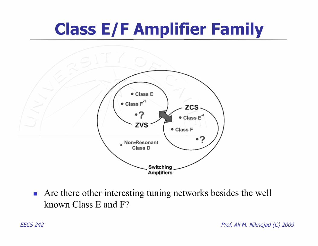
Class E/F Amplifier Family
Are there other interesting tuning networks besides the well known Class E and F?
EECS 242 Prof. Ali M. Niknejad (C) 2009
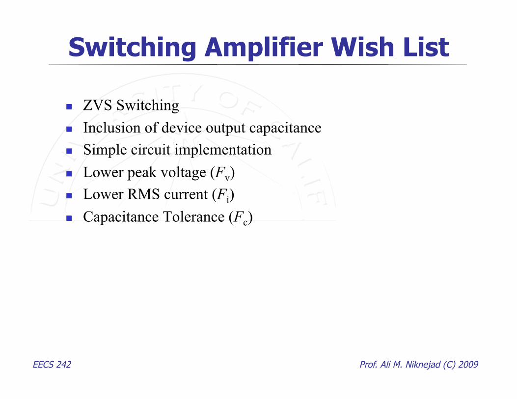
Switching Amplifier Wish List
ZVS Switching Inclusion of device output capacitance Simple circuit implementation Lower peak voltage (Fv) Lower RMS current (Fi) Capacitance Tolerance (Fc)
EECS 242 Prof. Ali M. Niknejad (C) 2009
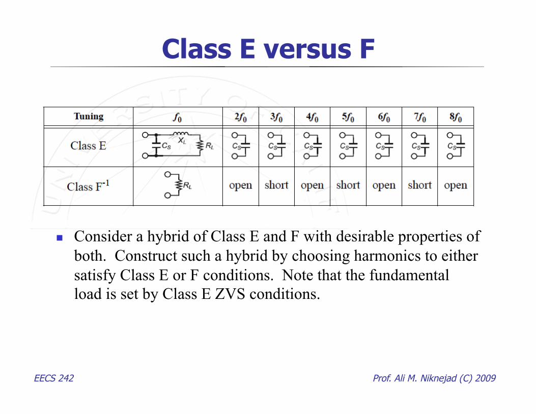
Class E versus F
Consider a hybrid of Class E and F with desirable properties of both. Construct such a hybrid by choosing harmonics to either satisfy Class E or F conditions. Note that the fundamental load is set by Class E ZVS conditions.
EECS 242 Prof. Ali M. Niknejad (C) 2009
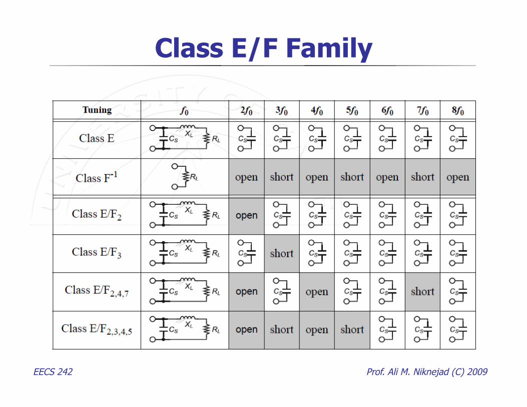
Class E/F Family
EECS 242 Prof. Ali M. Niknejad (C) 2009
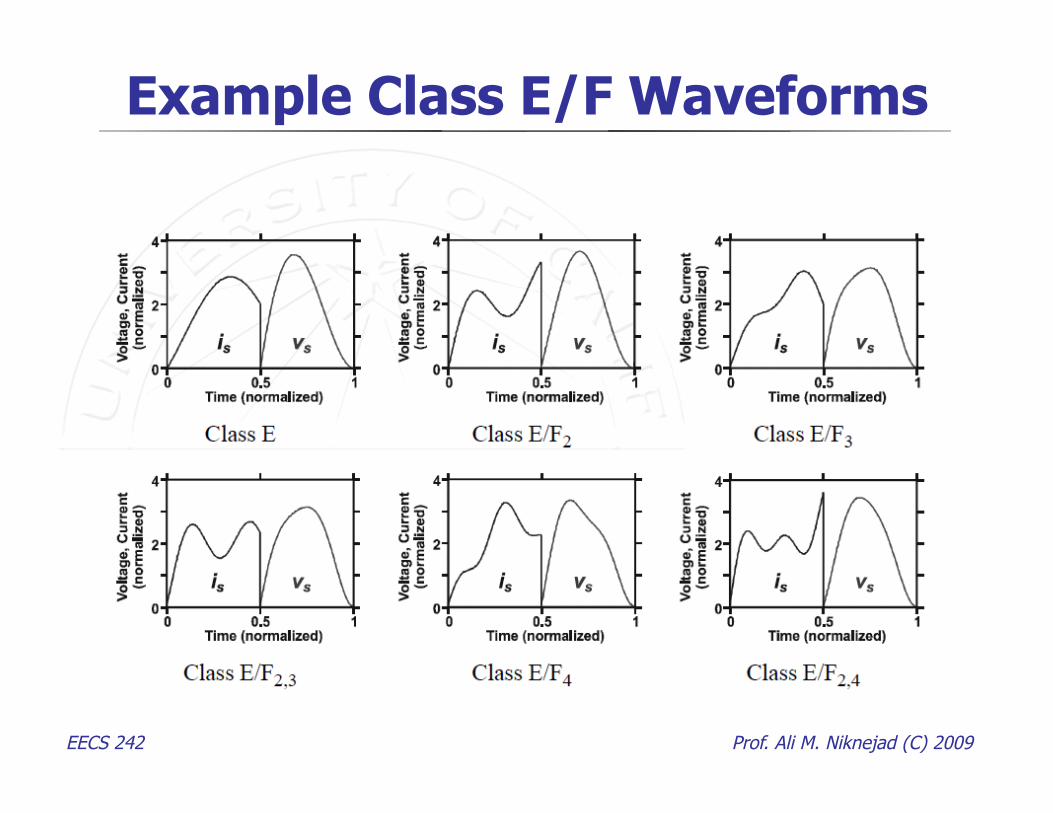
Example Class E/F Waveforms
EECS 242 Prof. Ali M. Niknejad (C) 2009
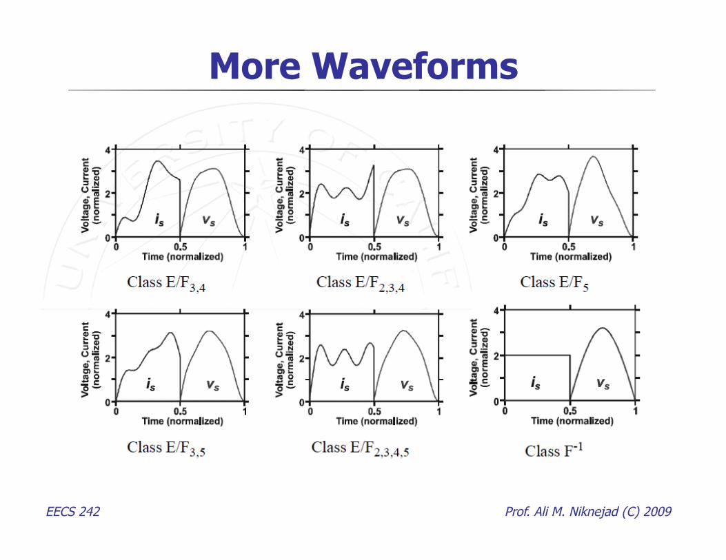
More Waveforms
EECS 242 Prof. Ali M. Niknejad (C) 2009
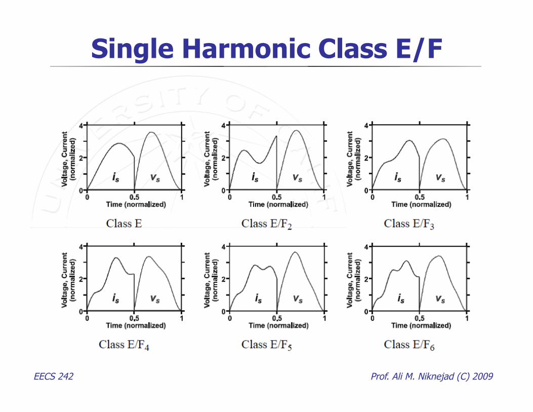
Single Harmonic Class E/F
EECS 242 Prof. Ali M. Niknejad (C) 2009
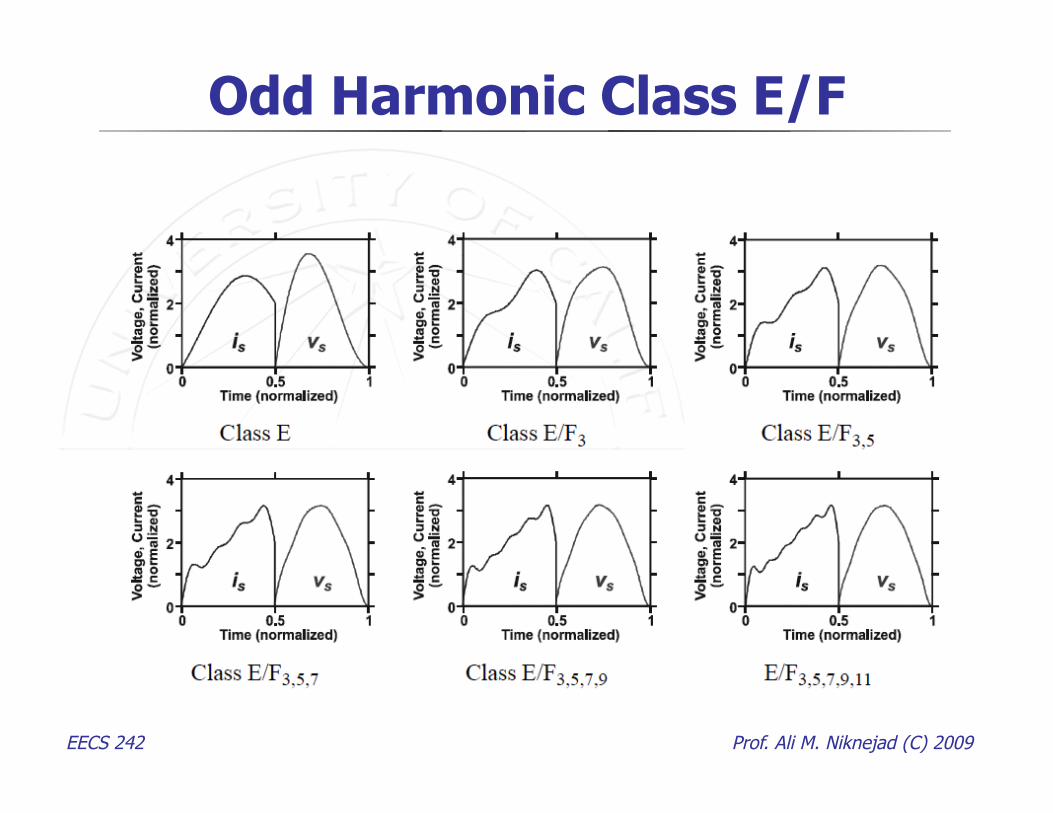
Odd Harmonic Class E/F
EECS 242 Prof. Ali M. Niknejad (C) 2009
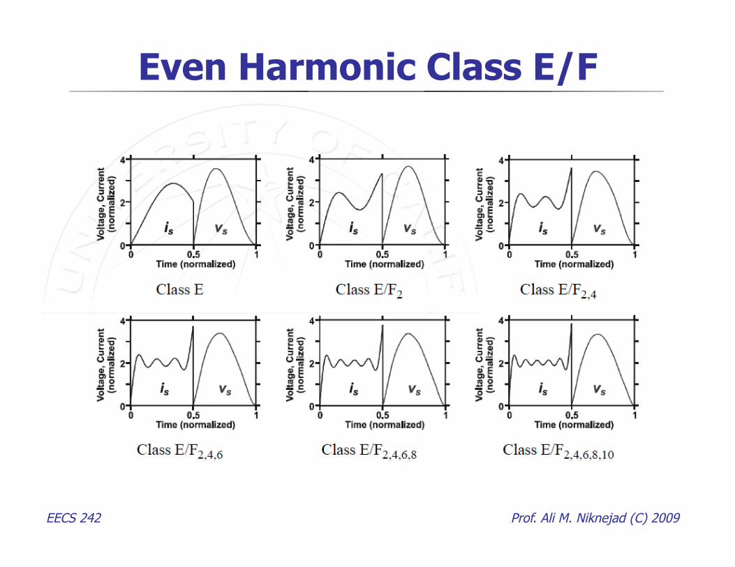
Even Harmonic Class E/F
EECS 242 Prof. Ali M. Niknejad (C) 2009
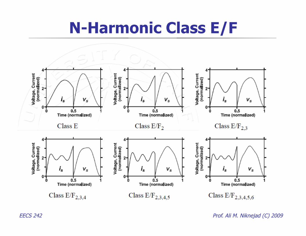
N-Harmonic Class E/F
EECS 242 Prof. Ali M. Niknejad (C) 2009
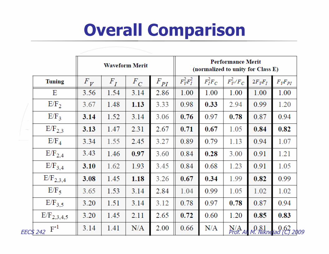
Overall Comparison
EECS 242 Prof. Ali M. Niknejad (C) 2009
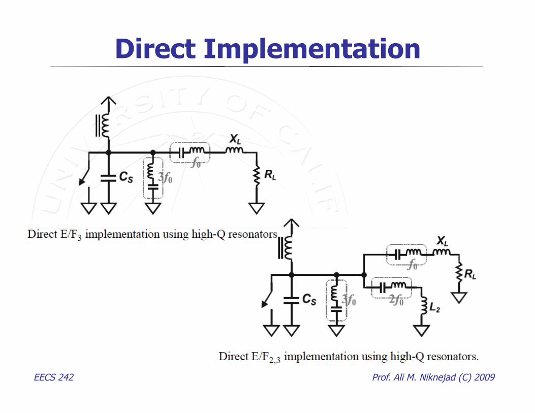
Direct Implementation
EECS 242 Prof. Ali M. Niknejad (C) 2009
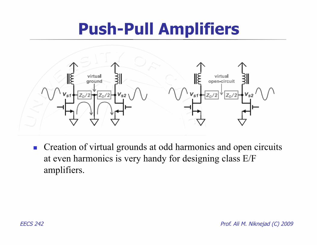
Push-Pull Amplifiers
Creation of virtual grounds at odd harmonics and open circuits at even harmonics is very handy for designing class E/F amplifiers.
EECS 242 Prof. Ali M. Niknejad (C) 2009
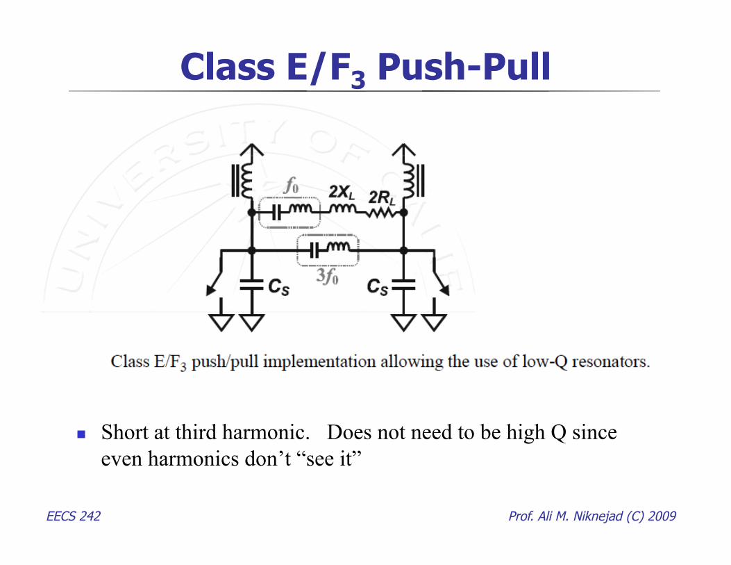
Class E/F3 Push-Pull
Short at third harmonic. Does not need to be high Q since even harmonics don’t “see it”
EECS 242 Prof. Ali M. Niknejad (C) 2009
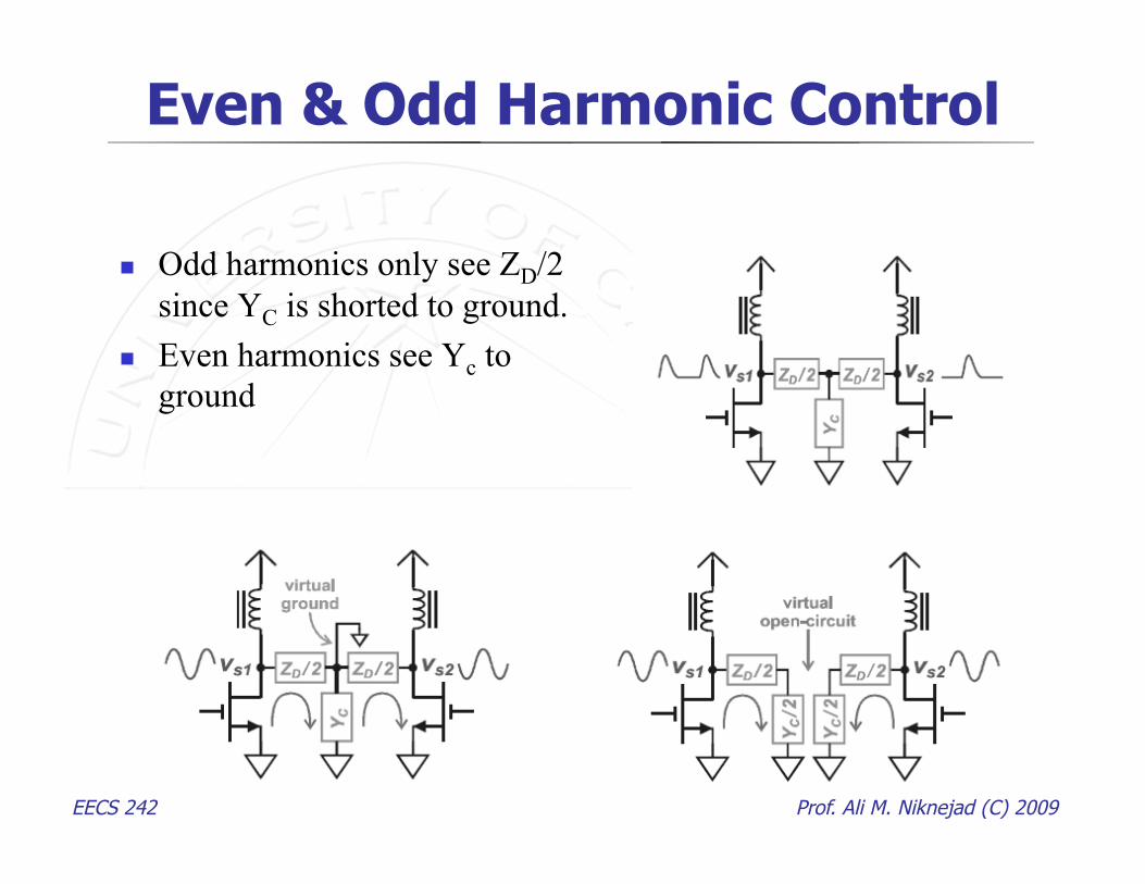
Even & Odd Harmonic Control
Odd harmonics only see ZD/2 since YC is shorted to ground.
Even harmonics see Yc to ground
EECS 242 Prof. Ali M. Niknejad (C) 2009
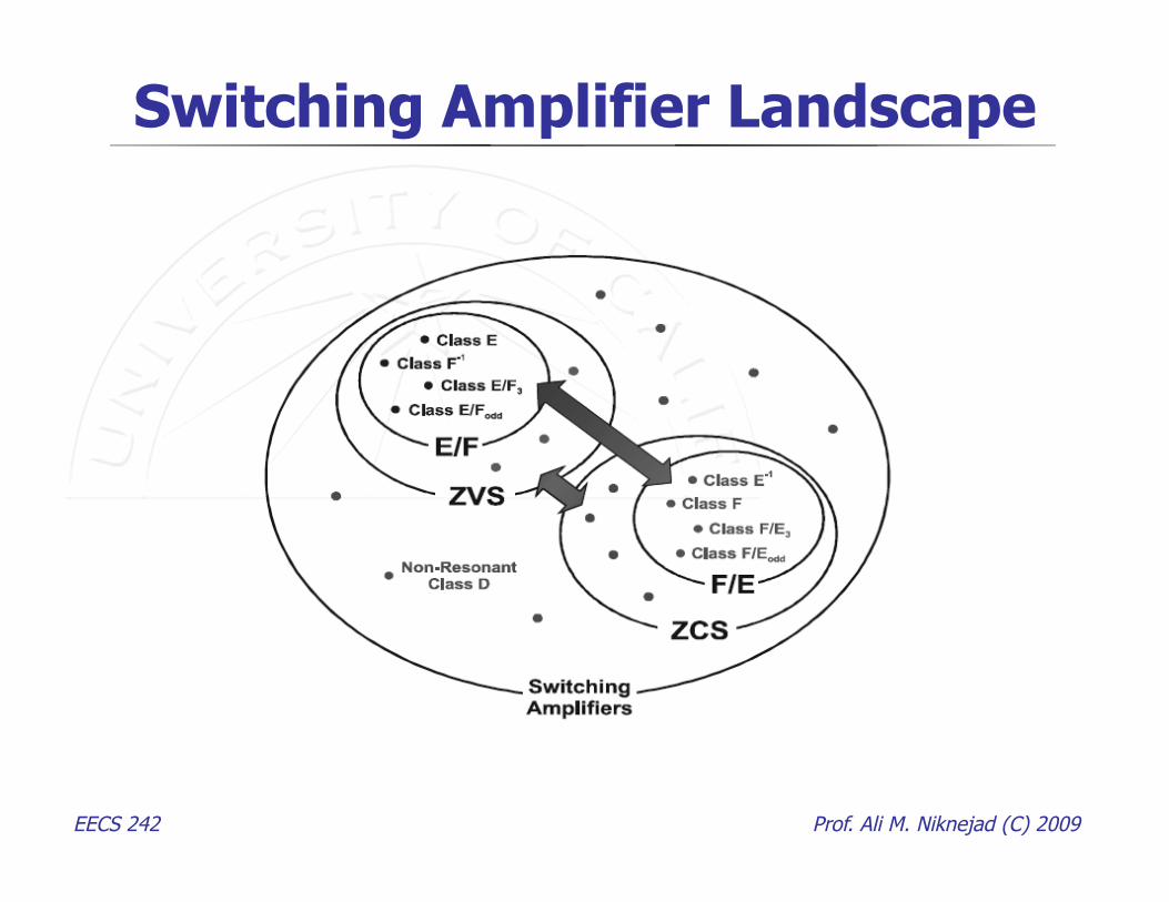
Switching Amplifier Landscape
EECS 242 Prof. Ali M. Niknejad (C) 2009
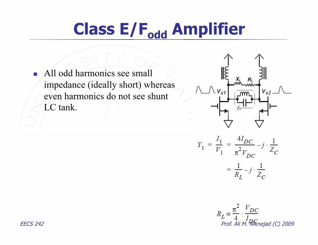
Class E/Fodd Amplifier
All odd harmonics see small impedance (ideally short) whereas even harmonics do not see shunt LC tank.
EECS 242 Prof. Ali M. Niknejad (C) 2009